1
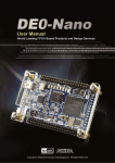
ECE 4434 - Advanced Digital Systems
Lab Manual
September 14, 2012
Contents
0.1
0.2
Objective . . . . . . . . . . . . . . . . . . . . . . . . . . . . . . . . . . . . . . . . . .
Introduction . . . . . . . . . . . . . . . . . . . . . . . . . . . . . . . . . . . . . . . . .
5
6
1 The DE2–115 Development Board and Quartus
1.1 DE2–115 Development Board . . . . . . . . . . .
1.2 Quartus II CAD Environment . . . . . . . . . . .
1.2.1 Design Entry . . . . . . . . . . . . . . . .
1.2.2 Project Processing . . . . . . . . . . . . .
1.2.3 Project Verification . . . . . . . . . . . . .
1.2.4 Device Programming . . . . . . . . . . . .
II
. .
. .
. .
. .
. .
. .
.
.
.
.
.
.
.
.
.
.
.
.
.
.
.
.
.
.
.
.
.
.
.
.
.
.
.
.
.
.
.
.
.
.
.
.
.
.
.
.
.
.
.
.
.
.
.
.
.
.
.
.
.
.
.
.
.
.
.
.
.
.
.
.
.
.
.
.
.
.
.
.
.
.
.
.
.
.
.
.
.
.
.
.
.
.
.
.
.
.
.
.
.
.
.
.
.
.
.
.
.
.
.
.
.
.
.
.
7
7
9
9
9
9
9
2 Schematic Capture Design – 4 Bit Counter
2.1 Design Entry . . . . . . . . . . . . . . . . .
2.2 Schematic Capture . . . . . . . . . . . . . .
2.3 Pin Assignment . . . . . . . . . . . . . . . .
2.4 Design Processing (Compiling) . . . . . . .
2.5 Device Programming . . . . . . . . . . . . .
.
.
.
.
.
.
.
.
.
.
.
.
.
.
.
.
.
.
.
.
.
.
.
.
.
.
.
.
.
.
.
.
.
.
.
.
.
.
.
.
.
.
.
.
.
.
.
.
.
.
.
.
.
.
.
.
.
.
.
.
.
.
.
.
.
.
.
.
.
.
.
.
.
.
.
.
.
.
.
.
.
.
.
.
.
.
.
.
.
.
.
.
.
.
.
11
11
19
22
24
24
7 Segment Display
. . . . . . . . . . . . .
. . . . . . . . . . . . .
. . . . . . . . . . . . .
. . . . . . . . . . . . .
.
.
.
.
.
.
.
.
.
.
.
.
.
.
.
.
.
.
.
.
.
.
.
.
30
30
31
32
38
3 Hardware Description Language
3.1 Background . . . . . . . . . . .
3.2 Design Entry – VDHL . . . . .
3.2.1 VHDL Syntax . . . . .
3.3 Pin Assignments and Results .
Design
. . . . .
. . . . .
. . . . .
. . . . .
.
.
.
.
.
.
.
.
.
.
.
.
.
.
.
(HDL) –
. . . . . .
. . . . . .
. . . . . .
. . . . . .
.
.
.
.
.
4 Combined Schematic Capture / HDL Design Example – 4 Bit counter with 7
Segment Display
41
4.1 Hybird Design Entry Techniques . . . . . . . . . . . . . . . . . . . . . . . . . . . . . 41
4.2 Pin Assignments and Results . . . . . . . . . . . . . . . . . . . . . . . . . . . . . . . 45
1
List of Figures
1.1
1.2
1.3
Top View of DE2–115 Development Board . . . . . . . . . . . . . . . . . . . . . . . .
Block Diagram of DE2–115 Architecture . . . . . . . . . . . . . . . . . . . . . . . . .
Digital Design Flow in Quartus II . . . . . . . . . . . . . . . . . . . . . . . . . . . . .
8
8
10
2.1
2.2
2.3
2.4
2.5
2.6
2.7
2.8
2.9
2.10
2.11
2.12
2.13
2.14
2.15
2.16
2.17
2.18
2.19
2.20
2.21
2.22
4 bit Binary Counter Example . . . . . . . . . . . . . .
Main Quartus II interface . . . . . . . . . . . . . . . . .
New Project Wizard Initial Step . . . . . . . . . . . . .
New Project Wizard Initial Step 1 . . . . . . . . . . . .
New Project Wizard Initial Step 2 . . . . . . . . . . . .
New Project Wizard Initial Step 3: Choosing Device . .
New Project Wizard Initial Step 4 . . . . . . . . . . . .
Create a new Design Document . . . . . . . . . . . . . .
Adding Symbol to Schematic Capture . . . . . . . . . .
LPM Counter Mega Wizard Step 1 . . . . . . . . . . . .
LPM Counter Mega Wizard Step 2 . . . . . . . . . . . .
Completed 4–bit Counter Schematic . . . . . . . . . . .
Access to Pin Planner . . . . . . . . . . . . . . . . . . .
Main Pin Planner Window . . . . . . . . . . . . . . . .
Access to the Compiler . . . . . . . . . . . . . . . . . . .
Device Configuration Window. Used to set correct Flash
Access Programming Interface . . . . . . . . . . . . . .
Default Programming Interface Window . . . . . . . . .
Switching to Active Serial Programming Mode . . . . .
Programming file extension .pof . . . . . . . . . . . . . .
Fully Configured Programming Interface Window . . . .
Experimental Results: 4 LEDs counting up . . . . . . .
. . . . . . . . . .
. . . . . . . . . .
. . . . . . . . . .
. . . . . . . . . .
. . . . . . . . . .
. . . . . . . . . .
. . . . . . . . . .
. . . . . . . . . .
. . . . . . . . . .
. . . . . . . . . .
. . . . . . . . . .
. . . . . . . . . .
. . . . . . . . . .
. . . . . . . . . .
. . . . . . . . . .
Memory Device
. . . . . . . . . .
. . . . . . . . . .
. . . . . . . . . .
. . . . . . . . . .
. . . . . . . . . .
. . . . . . . . . .
.
.
.
.
.
.
.
.
.
.
.
.
.
.
.
.
.
.
.
.
.
.
.
.
.
.
.
.
.
.
.
.
.
.
.
.
.
.
.
.
.
.
.
.
.
.
.
.
.
.
.
.
.
.
.
.
.
.
.
.
.
.
.
.
.
.
.
.
.
.
.
.
.
.
.
.
.
.
.
.
.
.
.
.
.
.
.
.
.
.
.
.
.
.
.
.
.
.
.
.
.
.
.
.
.
.
.
.
.
.
.
.
.
.
.
.
.
.
.
.
.
.
.
.
.
.
.
.
.
.
.
.
11
12
13
14
15
16
17
18
19
20
21
21
22
23
24
25
26
27
27
28
28
29
3.1
3.2
3.3
3.4
3.5
3.6
3.7
3.8
3.9
3.10
3.11
3.12
Seven Segment Display . . . . . . . . . . . . . . . . . . .
Display Converter 4 bit input to 7 Segment Display . .
Create New VHDL File . . . . . . . . . . . . . . . . . .
Project Navigator: Files . . . . . . . . . . . . . . . . . .
Project Navigator: Set Top Level Entity . . . . . . . . .
Insert Template Button . . . . . . . . . . . . . . . . . .
Entity Declaration Template . . . . . . . . . . . . . . .
Architecture Template . . . . . . . . . . . . . . . . . . .
VDHL file with default templates added . . . . . . . . .
Final VHDL file with all modifications made . . . . . .
Final Pin Planner Window . . . . . . . . . . . . . . . .
Experimental Result of working program for Example 2
.
.
.
.
.
.
.
.
.
.
.
.
.
.
.
.
.
.
.
.
.
.
.
.
.
.
.
.
.
.
.
.
.
.
.
.
.
.
.
.
.
.
.
.
.
.
.
.
.
.
.
.
.
.
.
.
.
.
.
.
.
.
.
.
.
.
.
.
.
.
.
.
.
.
.
.
.
.
.
.
.
.
.
.
.
.
.
.
.
.
.
.
.
.
.
.
.
.
.
.
.
.
.
.
.
.
.
.
.
.
.
.
.
.
.
.
.
.
.
.
.
.
.
.
.
.
.
.
.
.
.
.
.
.
.
.
.
.
.
.
.
.
.
.
.
.
.
.
.
.
.
.
.
.
.
.
.
.
.
.
.
.
.
.
.
.
.
.
.
.
.
.
.
.
.
.
.
.
.
.
.
.
.
.
.
.
.
.
.
.
.
.
30
31
32
33
34
34
35
35
36
37
39
40
4.1
4.2
4.3
4.4
Binary Counter Connected to the
Create Symbol for VHDL Code
Adding Bin to Hex Symbol . . .
Finished Hybrid Schematic . . .
Segment Display . .
. . . . . . . . . . . . .
. . . . . . . . . . . . .
. . . . . . . . . . . . .
.
.
.
.
.
.
.
.
.
.
.
.
.
.
.
.
.
.
.
.
.
.
.
.
.
.
.
.
.
.
.
.
.
.
.
.
.
.
.
.
.
.
.
.
.
.
.
.
.
.
.
.
.
.
.
.
.
.
.
.
41
43
44
44
7
.
.
.
2
4.5
4.6
Final Pin Planner Window . . . . . . . . . . . . . . . . . . . . . . . . . . . . . . . .
Experimental Result of working program for Example 2 . . . . . . . . . . . . . . . .
3
46
47
List of Tables
2.1
Pin Assignments of Example 1 . . . . . . . . . . . . . . . . . . . . . . . . . . . . . .
22
3.1
Pin Assignments of Example 2 . . . . . . . . . . . . . . . . . . . . . . . . . . . . . .
38
4.1
Pin Assignments of Example 3 . . . . . . . . . . . . . . . . . . . . . . . . . . . . . .
45
4
0.1
Objective
To give a brief introduction into the DE2–115 development board with emphasis on the following:
• Schematic capture in Quartus II CAD enviroment
• VHDL in Quartus II CAD enviroment
• Using the above to program the DE2–115 development board
Three short examples are provided to introduce you to FPGA design. Additional help can be found
in [1], [2], [3]. Please contact the TA for this lab for further information if needed. Note: this manual
is based on [4], the manual formally used for this course until FPGA and development board change.
5
0.2
Introduction
This document is to be used as an introductory guide for the ECE 4434 – Advanced Digital Design
labs, at The University of Western Ontario. It contains the basic information to create many digital
systems on the DE2–115 development boards using Quartus II CAD tool. The manual introduces the
design process using a set of examples to guide a user through the most common steps in designing
and prototyping a digital system on the DE2-115 development Board.
This manual is organized into the following chapters:
• Chapter 1: General information is presented about the DE2–115 Development Board and
Quartus II CAD environment.
• Chapter 2: A simple four bit binary counter design example is introduced and used to show the
common steps associated with schematic capture design entry, functional simulation, design
implementation, and programming the FPGA located on the DE2-115 Development board.
• Chapter 3: A four bit binary to seven segment LED design example is introduced to illustrate
the common steps associated with hardware description language design entry in VHDL logic
synthesis, functional simulation, and programming on the FPGA.
• Chapter 4: The four bit binary counter and the binary to seven segment LED examples
presented in Chapters 2 and 3 are combined to illustrate how designs can be created using
hybrid schematic capture techniques and a hardware description language. The final design is
then uploaded to the DE2–115 Development board.
6
Chapter 1
The DE2–115 Development Board
and Quartus II
1.1
DE2–115 Development Board
The development board that is used in the ECE4434 labs is the DE2–115 Development board from
Altera, Fig. 1.1. The main component of the DE2–115 is the FPGA. The FPGA used in this board
is the Altera Cyclone IV E Series – EP 4CE115F 29C7. Along with this state of the art FPGA, the
development board contains 2MB of SRAM, 8 MB of Flash memory, 4 Push–buttons, 18 switches,
18 Red LEDs, 9 Green LEDs, 50 MHz clock references, etc, [3]. The Main hardware features that
will be used in these labs are the switches, LEDs, 7 Segment displays and the clock references. A
block diagram of the DE2–115 is provided in Figure 1.2. The FPGA is programmed through the
USB connection on the back of the board. This is discussed in more detail in Section 2.5.
Additional information about the DE2–115 Development board can be found in [3]. For pin assignments please refer to appropriate example.
7
Figure 1.1: Top View of DE2–115 Development Board
Figure 1.2: Block Diagram of DE2–115 Architecture
8
1.2
Quartus II CAD Environment
The DE2–115 Development board is programmed by using the Quartus II CAD environment. This
tool allows basic to complex digital designs to be created and uploaded to the FPGA. Quartus II
12.0 Web Edition is used in these labs. Please use this edition if programming on home computers
to ensure compatibility in lab machines. Quartus II only runs on Windows or Linux Based machines
This manual will provide a brief introduction to Quartus II however, for a more detailed tutorial
please read [2].
The general design flow for Quartus II is highlighted in Figure 1.3. These blocks make up the
Design Entry, Project Processing, Project Verification, and Device Programming of the overall design
flow. Each will be briefly described below:
1.2.1
Design Entry
This stage of the design cycle is specified by the input types recognized by Quartus II design environment. Quartus II supports design entry using schematic capture (block based design), hardware
description languages (VHDL, Verilog, AHDL), system level design, or a combination of these techniques.
1.2.2
Project Processing
This step of the design flow converts the high level design (schematic, HDL, etc) to low–level logic.
This process is called synthesization. Altera tools such as Quartus II support this for various HDL’s
such as VHDL, Verilog, AHDL, etc. When a design is done using schematic capture a netlist is
created to allow the components to be mapped to the targets FPGA. This step converts the design
information into a form that can be used to verify the design by simulation or to be programmed in
a later step.
1.2.3
Project Verification
This phase validates the logical function of the design before it is programmed to a FPGA device.
Most the errors found in this phase are relatively small and can be corrected by adjusting the design.
During this phase timing and various other limitations of the design are tested. This is often referred
to as the simulation phase.
1.2.4
Device Programming
The lower–level code that was produced in the previous stages is used to upload directly to the
FPGA or flash memory. There are two main methods of programming: JTAG and AS mode. JTAG
programs the FPGA directly and AS mode programs flash memory. This process is discussed in
detail in Section 2.5.
9
Figure 1.3: Digital Design Flow in Quartus II
10
Chapter 2
Schematic Capture Design – 4 Bit
Counter
In this chapter, a simple 4–bit binary counter will be used to illustrate the steps needed to create
a digital design using the schematic block method. This design will be created using Quartus
II’s schematic capture interface,[5], verified and compiled for the DE2–115 development board. The
binary counter design is shown in block diagram form in Figure 2.1. The main blocks of this example
are the 50 M Hz clock, divider logic to lower the clock frequency, 4 bit binary counter, and finally
4 LEDs. The clock and the LEDs are located externally on the DE2–115 board, while the divider
logic and counter are programmed into the FPGA. The counter is clocked to a lower frequency to
allow the user to see the LEDs changing. Each step of the design process is outlined in the following
sections.
4 LEDs
Divider Logic
(LPM_Counter)
50 MHz
Clock
Lower Freq
Clock
4-bit Binary Counter
(4Count)
Figure 2.1: 4 bit Binary Counter Example
2.1
Design Entry
To begin this new digital design, one must first start Quartus II. Once, opened a new project should
be created. The main Quartus II interface is shown in Fig. 2.2. To create a new project click on the
New Project Wizard. The following figures guide the user through the wizard, Fig. 2.3 – Fig. 2.7.
This process is repeated throughout each example and project made. Note, in Fig. 2.6 the device
used is EP4CE115F29C7. This must be chosen to be the exact FPGA used in the labs or errors
may occur when programming. The project wizard allows the user to add extra files or libraries to
the project as well.
Once the project is created, we will open the schematic capture window. To do this click File–New,
the following window appears. Here you can create, Block diagrams, VHDL, Verilog, etc designs,
Fig. 2.8. From the new window, we can now create the schematic for the 4–bit counter.
11
Figure 2.2: Main Quartus II interface
12
Figure 2.3: New Project Wizard Initial Step
13
Figure 2.4: New Project Wizard Initial Step 1
14
Figure 2.5: New Project Wizard Initial Step 2
15
Figure 2.6: New Project Wizard Initial Step 3: Choosing Device
16
Figure 2.7: New Project Wizard Initial Step 4
17
Figure 2.8: Create a new Design Document
18
2.2
Schematic Capture
In the new schematic created, we will create the 4–bit counter, which contains 2 main components:
LPM counter and 4–bit count. To place components on the schematic double click any white space on
the screen or click the AND gate symbol in the menu bar. This will launch the Symbols/Components
Selection Window, as shown in Fig. 2.9. Inside, this window a user can create high–level structures
such as ROMs, etc down to low–level blocks such as gates. These components are found in the
different libraries available.
The 4–bit binary counter example will require Input, Output symbols, 4–bit binary counter
(4Count), and a LPM Counter. 4Count is located in the others library under the maxplus2 folder
and LPM Counter is found in the Megafunctions library under arithmetic. The input and output
pins are found under the primitives library under the folder pin. Also, a ground and vcc pins are
needed, they are found under the primitives library under the folder other.
The LPM Counter symbol is a parameterized macro. When this component is selected and entered
into the schematic the following window appears, Fig. 2.10. The output file for the LPM Counter
is selected to be VHDL. The next few screens in the MegaWizard configure the LPM Counter. In
this example the output bus will be 32 bits wide and the counter will count up to 24 bits where
the output clock is connected to the 4 count, Fig. 2.11. All other options can be left to default, or
you can click finish. Placed the finished symbol on the main schematic capture window. The input
to the LPM counter is the clock on the DE2–115. Connect an input pin to the Clock terminal of
the LPM counter and label it CLK. The output of the LPM Counter is the Q bus. To label a bus
in Quartus II the following label is used: q[31..0]. Bus names usually have the structure bus name
[Most significant element number..least significant element number]. To extract a single element
from the the bus label an individual wire the specific node needed. For example to extract line 24
use the label q24.
Figure 2.9: Adding Symbol to Schematic Capture
The 4Count component is not a macro and can be placed directly on the schematic. Once all components are added to the schematic capture window, complete the schematic as shown in Fig. 2.12.
Once this is complete we can associate the input and output pins to pins on the FPGA.
19
Figure 2.10: LPM Counter Mega Wizard Step 1
20
Figure 2.11: LPM Counter Mega Wizard Step 2
Figure 2.12: Completed 4–bit Counter Schematic
21
2.3
Pin Assignment
The FPGA used, EP4CE115F29C7, contains many pins which are directly hardwired to physical
items on the DE2–115. To assign the pins in the schematic file we must assign the specific pin
location to our input/output pins. To do this you first must open the Pin Planner Tool. It is found
under Assignments–Pin Planner, Fig. 2.13. Once the Pin Planner main window is open, Fig. 2.14,
you can see the FPGA pictured above and the input/output pins below. In the bottom frame under
the location tab is where we will assign the specific pin location. The pin locations for each switch,
LED, 7 Seg, LCD etc, are located in the DE2–115 manual, [3]. In this lab every pin assignment
needed is given in the lab manual. If you wish to choose to use other hardware features you may
refer to the manual.
In this lab we have 1 input pin and 4 output pins. Our input pin is connected to the 50 MHz clock
reference and the output pins are connected to 4 LEDs. The DE2–15 contains three 50 MHz clock
references along with an external SMA clock input and output. We will be using one of the main
internal clock references. The pin location of this CLK is PIN AG14. Four red LEDs are used as
our outputs in this lab. The DE2–115 contains 18 red LEDs and 9 green LEDs. The complete Pin
Assignment list is shown in Table 2.1. The finished Pin Assignment window is shown in Fig. 2.14.
Once completed just close the window and the specific pins are now mapped to the correct input
and output pins.
Table 2.1: Pin Assignments of Example 1
I/O Description Label Pin Location
50 MHz Clock
Clk
PIN AG14
LED0
D1
PIN G19
LED1
D2
PIN F19
LED2
D3
PIN E19
LED3
D4
PIN F21
Figure 2.13: Access to Pin Planner
22
Figure 2.14: Main Pin Planner Window
23
2.4
Design Processing (Compiling)
Once the pin assignments are set we can compile our design. To compile the design press the purple
play button, Fig. 2.15. You can compile your design before making pin assignments but you have to
always re–compile after new pin assignments have been made in order to have the changes effect the
design output. As long as the Device was chosen correctly in Section 2.1 the compiler will correctly
compile the design for our FPGA. If this was not done in the Section 2.1 then the user must assign
a device by clicking Assignments–Device and then follow the process outlined in Fig. 2.6.
Once compilation is completed your design should have 0 errors. You have have some warnings
which are generally ok to have. One should always review the warnings before moving on to make
sure they are not critical. If you do have errors, please go back to our design and recheck for
functionality. Once fully compiled we can either simulate our design in Quartus II or program the
FPGA board to experimentally confirm our results. In these labs we will only be programming the
FPGA’s to confirm the experiments experimentally, rather then simulating the design. Simulation
is not covered in this guide however, if one wishes to learn simulation techniques in Quartus II there
are many guides showing how this is done.
Figure 2.15: Access to the Compiler
2.5
Device Programming
Once we have a fully compiled design we can then program the FPGA on the DE2–115. There
are two methods to program the FPGA, JTAG or the AS method. The JTAG method stores the
program inside the FPGA and will work as long as power is supplied. Once power is lost, the
program is also lost. It cannot retain the program upon startup. In the AS method or Active Serial
Programming as its also known, programs flash memory which the FPGA reads upon startup. This
allows for power to be lost but leaves the running program intact. This is the method that is used
in these labs.
To program the DE2–115 one must first plug in a USB cord to the USB blaster port, left most
USB port. This should already be connected in the labs. When programming, SW19 should be set
to Prog. This switch is located on the leftmost portion of the board near SW19. The other setting
of SW19 is run, this should be set when running any program. The board should be powered down
when switching SW19 between Run and Prog. The Red button turns the device on and off.
To start programming the DE2–115 in Quartus II, we first must tell it what type of Flash memory
we are using. This is a very important step, if this is set wrong programming might fail. To set
the memory device used, click on the Assignment menu – then click on device. Figure 2.16 displays
the device configuration window. Please match the exact parameters as displayed in the figure. The
EPCS64 is the configuration device used for the flash memory. Everything else should be left as
default. This should be done in any programming example or lab. This only needs to be completed
once per project, as it is saved in the settings. Its always best to re–compile the program after this
step to ensure the changes get updated.
Now that all the hardware and software settings are set we can initiate the programming process.
To start click on the top menu Tools–Programmer, Fig. 2.17. This displays the main programming
interface, Fig. 2.18. Here, we can see that the hardware setup uses the USB–Blaster and the Mode is
set to JTAG. If it does not say USB–Blaster, select hardware setup and choose USB–Blaster. If it is
still not working, contact your TA for further assistance. In most cases, the programming interface
defaults to JTAG mode. Use the drop down to select Active Serial Programming. By doing this,
24
Figure 2.16: Device Configuration Window. Used to set correct Flash Memory Device
25
Figure 2.17: Access Programming Interface
the following menu is displayed, Fig. 2.19, click yes. The programming mode will be changed to
Active Serial Programming. By doing this our compiled file must be reloaded. Click Add file from
the left hand menus. The file that should be added has the file extension .pof, Fig. 2.20. Once this
file has been added check the following boxes, Program/Configure, Verify, Blank–Check. The fully
configured programming interface is shown in Figure 2.21. To start programming press the start
button, the progress bar on the right will indicate when the programming is completed.
To test your program on the DE2–115, first turn off the device with the red button and flip the
switch to Run from Prog then turn the device back on. In this example the user does not have to
provide any input directly, therefore the four LEDs should start to count from 0 to 15 in binary,
Fig. 2.22. If they do not count up correctly, refer back to Section 2.2 to ensure your design is
functionally correct.
26
Figure 2.18: Default Programming Interface Window
Figure 2.19: Switching to Active Serial Programming Mode
27
Figure 2.20: Programming file extension .pof
Figure 2.21: Fully Configured Programming Interface Window
28
Figure 2.22: Experimental Results: 4 LEDs counting up
29
Chapter 3
Hardware Description Language
Design (HDL) – 7 Segment Display
In this chapter, a binary to seven segment display converter is designed. It will be designed using
VHDL rather then schematic capture.[6]. The VHDL code will be synthesized and then uploaded to
the DE2–115 Development board. The goal of this design will be to display the correct hexadecimal
symbol on a seven–segment LED display that corresponds to the four bit binary input provided by
the user using the switches provided.
3.1
Background
A single seven–segment display can be used to display the digits 0 through 9 and the Hex symbols
A through F by lighting up the appropriate sets of segments, Fig. 3.1. The seven segment displays
on the DE2–115 are active low circuits. Therefore, a logic 0 is needed to turn on a section in the 7
segment display.
Figure 3.1: Seven Segment Display
Figure 3.2 shows the block diagram of the binary to hex converter that is to be designed. The bin
to hex block contains all the logic necessary to drive the 7 segment display in a manner in which the
hexadecimal symbol associated with the four bit input is displayed. For example if all four switches
were low then the symbol 0 would be displayed and the symbol 8 if just I[3] switch is set to logic
high. There are a total of 16 possible input combinations which display the symbol 0 to F.
30
7 Segment
Display
Bin to Hex
Converter
I[3] I[2] I[1] I[0]
Figure 3.2: Display Converter 4 bit input to 7 Segment Display
3.2
Design Entry – VDHL
Rather than create our design using the schematic capture tool as in the first example, we will
instead create our design using a HDL or more specifically VHDL. Hardware Description Languages,
HDL, can be used to create simple designs to highly complex designs. HDLs are textual representations that are used to model the structure and or/ behaviour of the system hardware. HDLs have
special constructs that specifically designed to model the characteristics of digital and in some cases
analog hardware. The major difference between HDLs and higher level software languages are that
HDL’s can easily model the timing attributes and the highly concurrent aspects of digital hardware,
(i.e. parallel hardware computing). In addition HDL’s have the power to fully describe a logic
system using both behavioural and structural design techniques.
The two main HDL’s used are VHDL and Verilog. VHDL is used more by academia and Verilog
is used more by industry. The syntax of the two are very similar. If you know how to code in one
language it is very easy to move to the other language. In these labs we will be using VHDL to
design our systems.
This example will demonstrate how to create the binary to hex converter using VHDL. First a
new project must be created, refer to the directions outlined in Section 2.1. Once created we will
add the a new VHDL file to our project. First click File–New–VHDL file, Fig. 3.3. This creates
a blank VHDL document in your project. You must make sure that it is the top level file in the
project. To do this in the project navigator on the left side of the page click the files tab, Fig. 3.4
and right click and choose set as Top Level Entity, Fig. 3.5.
The VHDL file that represents the binary to hexadecimal converter design can now be directly
entered using the the text editor or using built in templates to set up the overall structure of the
VHDL code.
The built in VHDL templates provide the necessary keywords with the correct structure to create a
fully working VHDL design. In this example we will be using two templates, The Entity Declaration
and the Architecture templates. To insert a template into the design click the insert template button,
Fig. 3.6, which looks like a scroll type icon. By clicking this button, the Insert Template window
appears. Here, we can choose templates for all different kinds of HDLs. The first template we
are interested in is the Entity Template. It is found under VHDL–Constructs–Design Units–Entity,
Fig. 3.7. Press the Insert button to insert it into your code. Next, insert the Architecture Template
found under VHDL–Constructs–Design Units–Architecture, Fig. 3.8.
All VHDL files contain these two main sections, Entity and Architecture. The Entity section
describes how the current system interfaces to the outside world ( i.e. input and output) and the
Architecture section describes how the design is to function (i.e. details of the implementation).
Figure 3.9 shows the VHDL file with the templates added.
31
Figure 3.3: Create New VHDL File
Modify you VHDL code to match the one provided in Fig. 3.10. This shows the finalized VHDL
code with each section completed. The following subsection will describe the syntax and operation
of the VHDL code. This lab is not a major tutorial in VHDL, the course textbook along with online
resources provide more detailed tutorials.
3.2.1
VHDL Syntax
VHDL stands for Very High Speed Integrated Circuits Hardware Design Language. Like any computer language it has specific syntax to represent its operation. This section gives a brief overview of
the syntax used in this example. Double dashes, – –, are used to introduce comments and semicolons
are used to terminate the statements. The file begins with the VHDL keyword entity followed by
the user–defined name of the logic design (in this case bintohex). It is recommended to have the
entity name the same as the project name to prevent errors. In some cases the VHDL code will not
compile because of this.
The entity name is then followed by the keywords is port that designates that a list of input/output
ports is to follow. In this case, we need to define two bus signals. One is named I (for input) which
is a four member input vector (direction specified by the in keyword), I(3) – I(0), with I(3) acting as
the most significant bit (this is due to the downto keyword). The other is a seven member output
vector (direction specified by the out keyword) which is named O, which has seven members O(6)
– O(0). Note: The STD LOGIC VECTOR defines the vector type. It is declared in the library
IEEE.std logic 1164.all. This library should be added to every VHDL file done. It is possible for the
user to declare arbitrary data types in VHDL. The data types defined in this library are standardized
allowing for increased portability among VHDL simulators and synthesizers. The entity section ends
with the end statement followed by the design name.
The desired behaviour of the entity section is modelled in the architectural body section. This
section begins with the keyword architecture which is followed by a user defined name for the
architecture (in this case the bintohex arch is used) which is paired with the identity of the entity
using the of keyword followed by the entity name (i.e. in this case of bintohex). The begin keyword
is used to separate the architecture declarative part of the model from the architecture statement
32
Figure 3.4: Project Navigator: Files
part. The architecture declarative part is used to make declarations for such items type, signals,
and components (i.e. internal or local signals, local sub components). For the model presented in
Fig. 3.10, no declarations are needed to represent the design. The architecture statement part of
the model is placed between the begin keyword and the end keyword. This is where the VHDL
modelling statements are to be placed. A single with, select and when statement was added to
the architecture section. For a more detailed analysis in VHDL coding please consult your course
textbook and class notes.
33
Figure 3.5: Project Navigator: Set Top Level Entity
Figure 3.6: Insert Template Button
34
Figure 3.7: Entity Declaration Template
Figure 3.8: Architecture Template
35
Figure 3.9: VDHL file with default templates added
36
Figure 3.10: Final VHDL file with all modifications made
37
3.3
Pin Assignments and Results
Once the VHDL code is completed and compelled with no errors we can assign physical pins to the
inputs and outputs of the VHDL code. Follow the process outlined Section 2.3 to access the Pin
assignments menu. The inputs to this example are the 4 Switches and the output to this design
are the 7 segment display LEDs. These hardware pin locations are located in Table 3.1. The final
output of the Pin Planner is shown in Fig. 3.11.
Table 3.1: Pin Assignments of Example 2
I/O Description
Label Pin
Switch 0
I[0]
PIN AB28
Switch 1
I[1]
PIN AC28
Switch 2
I[2]
PIN AC27
Switch 3
I[3]
PIN AD27
Seven Segment 0
O[0]
PIN G18
Seven Segment 1
O[1]
PIN F22
Seven Segment 2
O[2]
PIN E17
Seven Segment 3
O[3]
PIN L26
Seven Segment 4
O[4]
PIN L25
Seven Segment 5
O[5]
PIN J22
Seven Segment 6
O[6]
PIN H22
Once completed re–compile and program the DE2–115 as described in Sections 2.4 and 2.5. When
the program is successfully loaded onto the DE2–115, the four switches should control the 7 Segment
Display. The user should test every combination to determine if the program is working correctly.
An example of the finished program when the input is 0011 and the output is 3 is shown in Fig. 4.6
38
Figure 3.11: Final Pin Planner Window
39
Figure 3.12: Experimental Result of working program for Example 2
40
Chapter 4
Combined Schematic Capture /
HDL Design Example – 4 Bit
counter with 7 Segment Display
In this chapter, the two previous design examples from Chapter 2 (the binary counter) and Chapter
3 (the binary to seven segment hexadecimal converter) are combined to form a complete hexadecimal
counter design. The final design will result in a new hexadecimal symbol being displayed on the
built-in seven segment LED after each master clock pulse created from the 50 MHz clock going
through the LPM Counter.
The hexadecimal counter will be constructed by connecting the outputs of the binary counter
design directly to the inputs to the binary to seven segment hexadecimal converter as shown in
Figure 4.1. As in the binary counter example of Chapter 2, the clocking signal will originate from an
external 50MHz oscillator which will be directed through a 24 bit pre–scaler network. To minimize
the design effort and illustrate the mechanics of hybrid design methodology, this design is to be
entered using both schematic capture and VHDL.
7 Segment
Display
50 MHz
Clock
Divider Logic
(LPM_Counter)
Bin to Hex
Converter
Lower Freq
Clock
4-bit Binary Counter
(4Count)
Figure 4.1: Binary Counter Connected to the 7 Segment Display
4.1
Hybird Design Entry Techniques
This section presents a basic methodology which allows for hybrid hierarchical designs to be entered
using a combination of schematic capture and VHDL. The base methodology is demonstrated using
the hexadecimal counter example which was described in Chapter 2. The material in this chapter
41
assumes that the reader is already familiar with the basic design process of schematic capture and
VHDL coding found in the previous chapters.
The hexadecimal counter example will be created by combining the major components of the
binary counter example from Chapter 2, and the binary to hexadecimal converter from Chapter 3.
This is done by creating a symbol of the bin to hex converter. It is recommended that you open up
the example schematic created in Chap 2 and save it to another name for use in this final example.
This file is the main file we will add our symbol to. Re–save this schematic as bcounterw7seg.bdf.
Once completed, create a new project with the same name and during the process add this file to
the main project. When adding files to this project, add the VHDL files completed in the second
example, these will be used when creating the symbol.
Now we will create the symbol of the bin to hex converter. Open the VHDL file that you added
to the current project. The VHDL code should appear on the screen. To create a symbol, click File
– Create/Update – Create Symbol Files for Current File, Fig. 4.2. This creates the symbol to be
used in the schematic capture. The next step is to add the symbol to the main schematic window.
To do this click the add component button and find the bintohex symbol under Project – bintohex,
Fig. 4.3. The output of the 4–count should now be connected to the bintohex symbol with the
output pins modified. Name all pins according to the final schematic, shown in Figure 4.4. Save
the project and compile the project before assigning pins.
42
Figure 4.2: Create Symbol for VHDL Code
43
Figure 4.3: Adding Bin to Hex Symbol
Figure 4.4: Finished Hybrid Schematic
44
4.2
Pin Assignments and Results
Once the hybrid schematic is completed and compelled with no errors we can assign physical pins to
the inputs and outputs of the schematic. Follow the process outlined Section 2.3 to access the Pin
assignments menu. There are no direct inputs to this example other than the 50 MHz Clock and
the output to this design are the 7 segment display LEDs. These hardware pin locations are located
in Table 4.1. The final output of the Pin Planner is shown in Fig. 4.5.
Table 4.1: Pin Assignments of Example 3
I/O Description
Label Pin
50 MHz Clock
CLK
PIN AG14
Seven Segment 0
O[0]
PIN G18
Seven Segment 1
O[1]
PIN F22
Seven Segment 2
O[2]
PIN E17
Seven Segment 3
O[3]
PIN L26
Seven Segment 4
O[4]
PIN L25
Seven Segment 5
O[5]
PIN J22
Seven Segment 6
O[6]
PIN H22
Once completed re–compile and program the DE2–115 as described in Sections 2.4 and 2.5. When
the program is successfully loaded onto the DE2–115, the 7 Segment Display should count up from
0 to F. The user should watch this counting to determine if the program is working correctly. An
example of the finished program when the output is A is shown in Fig. 4.6
45
Figure 4.5: Final Pin Planner Window
46
Figure 4.6: Experimental Result of working program for Example 2
47
Bibliography
[1] Altera Corporation, Introduction to the Quartus II Software, 2010.
[2] Altera Corporation, Quick Start Guide for Quartus II Software, 2007.
[3] Terasic Technologies, DE2-115 User Manual, 2010.
[4] Sin Ming Loo B.Earl Wells, Altera’s MAX+Plus II and the UP 1 Education Board - A users
guide, The University of Alabama, Auguest 2001.
[5] Altera Corporation, Quartus II Introduction using Schematic Design, 2008.
[6] Altera Corporation, Quartus II Introduction using VHDL Design, 2010.
48