1
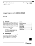
Freescale Semiconductor
Application Note
AN2868
Rev. 1, 11/2004
Using the MC9328MX21 (i.MX21) to Create a
VGA Digital Photo Album
by: Amanda McGregor
1
Abstract
This application note gives an overview of the
MC9328MX21 (i.MX21) processor’s Liquid Crystal
Display Controller (LCDC) functionality, and discusses
how the new graphics window feature can be used for
creating a VGA Digital Photo Album application with a
10.4” NEC VGA display.
2
Introduction
The i.MX21 processor’s LCDC is an enhanced version
of the LCDC found on the previous versions of the i.MX
family (i.MX1 and i.MXL). The i.MX21 processor’s
LCDC adds the following features:
• Supports displays up to 800 × 600.
• Supports color up to 18bpp—that is, 262K
different colors.
• Supports the management of a second display
area, called the “graphics window”, and blends
the graphics window with the main display area.
© Freescale Semiconductor, Inc., 2004. All rights reserved.
Contents
1
2
3
4
5
6
7
8
Abstract . . . . . . . . . . . . . . . . . . . . . . . . 1
Introduction . . . . . . . . . . . . . . . . . . . . . 1
i.MX21 LCDC Functional Overview . . 2
Use Case: VGA TFT LCD . . . . . . . . . . 10
VGA Digital Photo Album . . . . . . . . . 13
Conclusion . . . . . . . . . . . . . . . . . . . . . 25
Reference Documentation . . . . . . . . . 26
Revision History . . . . . . . . . Back Cover
i.MX21 LCDC Functional Overview
Many applications require the use of a VGA resolution display. On previous generations of i.MX it has
been difficult to support the bandwidth required by a VGA panel. Enhancements to the LCDC in the
i.MX21 processor enable the i.MX21 to easily support displays up to VGA resolution at 18bpp color
depth. This application note introduces the VGA Digital Photo Album application, specifically designed
to test the VGA capabilities of the i.MX21 processor’s LCDC and to demonstrate the new graphics
window feature.
3
i.MX21 LCDC Functional Overview
This section gives an overview of the features of the i.MX21 processor’s LCDC, in particular the graphic
window functionality, new to the i.MX21. Following this, a detailed functional description of the i.MX21
processor’s LCDC is given, including a description of the parameters important to its configuration. As
described previously, this section will focus on the application of the i.MX21 processor’s LCDC to drive
an active matrix (TFT) display.
3.1
i.MX21 Processor’s LCDC Sub-System
Figure 1 shows the functional block diagram of the i.MX21 processor’s LCDC for an active matrix display
with graphics window functionality enabled.
B a c k g r o u n d P la n e
DM A
B y te
Sw ap
F IF O
P a n n in g
D a ta
S h ifte r
DM A
B y te
Sw ap
F IF O
P a n n in g
D a ta
S h ifte r
LCDC
A r b ite r
G r a p h ic W in d o w
In te r fa c e
B u ffe r
C o lo r
C u rs o r
In te r fa c e
L o g ic
D is p la y
4bpp
8bpp
4bpp
8bpp
256x18
BGLUT
18bpp
256x18
GW LUT
18bpp
12bpp
16bpp
18bpp
A lp h a
B le n d in g
Figure 1. Block Diagram of Display Sub-System (8bpp Active Matrix)
As shown in Figure 1 there are two parallel data paths—one for the background plane and one for the
graphic window, called the foreground plane. Data for the background and foreground planes are fetched
from system memory (for example, SDRAM) via the LCDC’s internal DMA controller. The LCDC DMA
controller accesses the system memory using fixed length or dynamic burst length, depending on the
desired system performance. For a more heavily loaded system, the dynamic burst length option should be
selected to minimize system bus loading. Section 3.2.2, “LCD Size, Image Location in Memory, and Bus
Loading on page 4 discusses the bus loading effect for different panel sizes and burst options. Note that
the DMA settings for the background and foreground plane can be configured separately, however it is
common practice to set them to the same value.
Data for the foreground and background plane is fetched and loaded into the foreground and background
buffers, respectively. The buffers are each 32 × 32-word pixel buffers. Each buffer has a corresponding
Using the MC9328MX21 (i.MX21) to Create a VGA Digital Photo Album, Application Note, Rev. 1
2
Freescale Semiconductor
i.MX21 LCDC Functional Overview
high and low watermark value associated with it. When in dynamic burst mode, data is loaded into the
buffer until the number of empty words in the buffer equals the high watermark minus 2. When in fixed
burst mode, the burst length (in words) is equal to the high watermark. When the number of words left in
the buffer equals the low watermark, a DMA request is triggered.
After data is loaded into the buffer, the LCDC performs byte swapping on the data if an endianness change
is required, followed by panning operations, if panning is selected. If the data is 4bpp or 8bpp format, then
the 4bpp or 8bpp data is used as an index into a 256 × 18-bit look-up table to generate an 18-bit color. Data
of 12bpp, 16bpp, and 18bpp does not use the look-up table.
The background data and graphics window data then goes to the alpha blending module, which mixes the
background and graphics window according to the alpha value or color key, whichever mode is selected,
and generates a single image to be displayed.
After the alpha blending module, the color cursor is overlaid with the data to be displayed. The data then
goes into a buffer, goes through the interface logic, and is sent to the display.
3.2
i.MX21 Processor’s LCDC Configuration
There are many different parameters that need to be set to enable proper functioning of the LCDC with the
target display. This section outlines the parameters that need to be configured, the corresponding registers
that the parameters are stored in, and in some cases, example code of how to set these parameters. This
section also discusses the timing considerations for an LCD, which depends on the resolution of the
display.
3.2.1
LCDC Clock Configuration
Configuring the LCDC clock is one of the most critical tasks in establishing a correctly functioning LCDC
and display. Figure 2 shows the clock sources to the LCDC, as well as the output clock that is sent to the
display. Note that the diagram depicts an 18bpp active matrix (TFT) display.
Shift Register
32x32
Pixel Buffer
Memory + ARM926EJ-S
Data
Input
LD[0…17]
DMA Data Input
SysPLL
BCLKDIV
To 18bpp
TFT display
HCLK
Divide by 1...16
SysPLL
PERDIV3
Divide by 1...64
PERCLK3
PCD
Divide by 1…64
LCDC
LSCLK
Figure 2. LCDC Input and Output Clocks
Using the MC9328MX21 (i.MX21) to Create a VGA Digital Photo Album, Application Note, Rev. 1
Freescale Semiconductor
3
i.MX21 LCDC Functional Overview
Figure 2 illustrates the two clock sources of the LCDC. The description of the clocks follow:
• HCLK—Generated from the System PLL frequency and the value of BCLKDIV (bits [13:10]) in
the Clock Source Control Register (CSCR). Typically the System PLL is set to 266 MHz. At reset,
BCLKDIV has a value of 1, meaning that HCLK is BCLK divided by 2—that is, 133 MHz.
• PERCLK3—Generated from the System PLL frequency and the value of PERDIV3 (bits [21:16])
in the Peripheral Clock Divider Register 1 (PCDR1). PERCLK3 is exclusively used by the LCDC.
At reset, PERDIV3 has a value of 7, meaning that PERCLK3 is BCLK divided by 8—that is,
33.25 MHz.
The LCDC generates a clock for internal use by the data shift register to control the rate at which data is
sent to the display, PIXCLK, and an interface clock that is sent externally to the display, LSCLK, for
latching the pixel data.
• PIXCLK—Generated from PERCLK3 and the value of PCD (bits [5:0]) in the LCDC Panel
Configuration Register (LPCR). It is used for latching the pixel data into the shift register internal
to the LCDC, in preparation for sending out to the display. For a color TFT display, PIXCLK is the
same as LSCLK1. At reset, PCD has a value of 0, meaning that PIXCLK is PERCLK divided
by 1—that is, 33.25 MHz.
• LSCLK—Generated from PERCLK3 and the value of PCD (bits [5:0]) in the LCDC Panel
Configuration Register (LPCR). It is sent externally to the display for latching of the pixel data into
the display’s shift registers. Like the PIXCLK, LSCLK is 33.25 MHz out of reset.
The LSCLK value must be at least one third of the HCLK frequency in TFT mode to ensure that data is
output correctly from the LCDC. Otherwise, timing problems occur and the output from the LCDC is
unpredictable. HCLK can be set to a maximum of 133 MHz, meaning that LSCLK can be no faster than
44.3 MHz. This should be sufficient to meet the timing specifications of displays up to VGA resolution.
The frequency setting of LSCLK is determined by the display itself. The user will need to ensure that
LSCLK is set within the approved values as described in the display specification. Assuming the bus
bandwidth is sufficient to support the display resolution and frame rate, keeping the LSCLK within the
range specified in the panel specification should result in a flicker-free display. Visual verification of the
LSCLK frequency by probing LSCLK with an oscilloscope is recommended if problems are encountered.
Further information on the i.MX21 processor’s clocking scheme can be found in the i.MX21 Reference
Manual.
3.2.2
LCD Size, Image Location in Memory, and Bus Loading
The LCDC uses five parameters to determine the resolution of the panel, the starting memory address of
the image to be displayed, and how to get each successive line of data for display. The storage area in
memory is typically referred to as a “frame buffer”. The parameters are depicted in Figure 3.
1.
For a monochrome display, PIXCLK is faster than LSCLK by a factor equal to the number of pixels in an output vector.
Using the MC9328MX21 (i.MX21) to Create a VGA Digital Photo Album, Application Note, Rev. 1
4
Freescale Semiconductor
i.MX21 LCDC Functional Overview
Virtual Page Width (VPW)
SSA
Virtual
Page
Height
(VPH)
Screen Width
(XMAX)
Screen
Height
(YMAX)
Figure 3. LCD Screen Size Parameters
As shown in Figure 3, the screen size parameters are as follows:
• Screen Width (XMAX)—Indicates the width of the display, in terms of pixels divided by 16.
XMAX = Width of display (in pixels) / 16
•
Screen Height (YMAX)—Indicates the height of the display, in terms of the number of lines.
YMAX = Height of display (in pixels)
•
•
•
Screen Starting Address (SSA)—Starting address in memory of the active area of the frame
buffer—that is, the address of the first pixel to be displayed on the LCD, pixel (0,0). The screen
starting address can be modified, for example if you want to pan over another part of the frame
buffer.
Virtual Page Width (VPW)—Width of the frame buffer, in terms of the number of 32-bit words
required to hold the data for one “virtual” line. VPW is used to calculate the starting address of the
next line of data to be displayed on the LCD. Note that VPW may be larger than the width of the
display to allow panning over different areas of the frame buffer, however must represent at least
one full line of the resolution of the display to prevent artifacts on the LCD.
Virtual Page Height (VPH)—Height of the frame buffer. This value is not a parameter in the
LCDC register set, however is used in a software program for boundary checks when updating
frame buffer content.
Generally, the LCDC supports up to SVGA resolution—that is, 800 pixels wide by 600 pixels high.
However, the bandwidth required by an SVGA resolution display at 18-bit color is significant and the user
must ensure that enough system bandwidth is available such that an underrun error does not occur. An
underrun error occurs when the DMA cannot keep enough data in the LCDC FIFO, and the result is that
incorrect data is sent to the display. When the underrun error is corrected, the content on the display will
not be fixed until the next VSYNC is sent to the display.
We can calculate the theoretical bus load based on various LCD resolutions and color depths, assuming a
constant 60fps refresh rate. Table 1 shows the theoretical bus load, based on a fixed LCDC DMA burst
memory access of 8 words—that is, 8 × 32-bits. The calculations also assume that for each burst of 8
words, the total clock cycles required to read the data consists of 8 clocks of memory setup time plus 8
clocks to read back the 8 words of pixel data. This means that we are only receiving pixel data half of the
time, so a correction factor needs to be applied to the memory bandwidth calculation.
Using the MC9328MX21 (i.MX21) to Create a VGA Digital Photo Album, Application Note, Rev. 1
Freescale Semiconductor
5
i.MX21 LCDC Functional Overview
Maximum memory bandwidth = memory bus speed × bus width × correction factor
For example i.MX21, Max. Bus Bandwidth = 133MHz × 32-bits × 1/2 = 2128 Mbits/s
Table 1. Bus Bandwidth Comparison for Different Resolutions and Color Depths
Display Resolution Color Depth
Theoretical Bus Bandwidth
Theoretical i.MX21 Bus Load
(LCDC DMA fixed @ 8 words per burst,
HCLK = 133MHz)
QVGA (320 x 240)
8bpp
320 x 240 x 8bpp x 60fps = 37 Mbits/s
37 Mbits/s / 2128 Mbits/s = 1.7%
QVGA (320 x 240)
16bpp
320 x 240 x 16bpp x 60fps = 74 Mbits/s
74 Mbits/s / 2128 Mbits/s = 3.5%
QVGA (320 x 240)
18bpp
(unpacked)
320 x 240 x 32bpp x 60fps = 148 Mbits/s
148 Mbits/s / 2128 Mbits/s = 6.9%
VGA (640 x 480)
8bpp
640 x 480 x 8bpp x 60fps = 148 Mbits/s
VGA (640 x 480)
16bpp
640 x 480 x 16bpp x 60fps = 295 Mbits/s
295 Mbits/s / 2128 Mbits/s = 13.9%
VGA (640 x 480)
18bpp
(unpacked)
640 x 480 x 32bpp x 60fps = 590 Mbits/s
590 Mbits/s / 2128 Mbits/s = 27.7%
SVGA (800 x 600)
8bpp
800 x 600 x 8bpp x 60fps = 230 Mbits/s
230 Mbits/s / 2128 Mbits/s = 10.8%
SVGA (800 x 600)
16bpp
800 x 600 x 16bpp x 60fps = 461 Mbits/s
461 Mbits/s / 2128 Mbits/s = 21.7%
SVGA (800 x 600)
18bpp
(unpacked)
800 x 600 x 32bpp x 60fps = 922 Mbits/s
922 Mbits/s / 2128 Mbits/s = 43.3%
3.2.3
LCDC Active Matrix Interface Signals
Table 2 on page 6 provides the external signals generated by the LCDC and used by the active matrix
display. Note that passive matrix signals are not included in this table.
Table 2. LCD Controller Signal Description
Signal Name
Description
LD[17:0]
LCD Data Bus—All LCD signals are driven low out of reset and when LCDC is off.
VSYNC
Indicates the start of the next frame of data (called SPS for Sharp 320
HSYNC
Indicates the start of the next line of data.
LSCLK
Clock for latching data into the display driver’s internal shift register. Output from the LCDC, and must be less
than 1/3 of the HCLK (for TFT panels).
OE
Output enable signal to enable data to be shifted onto the display.
CONTRAST
Used to control the LCD bias voltage to modify the contrast of the display.
SPL_SPR
Sets the horizontal scan direction (for Sharp 320
PS
× 240 HR-TFT panel).
× 240 HR-TFT panels only).
Control signal output for source driver (for Sharp 320 × 240 HR-TFT panels only).
CLS
Start signal output for gate driver. This signal is an inverted version of PS (for Sharp 320
only).
REV
Signal for common electrode driving signal preparation (for Sharp 320
× 240 HR-TFT panels
× 240 panels only).
Using the MC9328MX21 (i.MX21) to Create a VGA Digital Photo Album, Application Note, Rev. 1
6
Freescale Semiconductor
i.MX21 LCDC Functional Overview
3.2.4
Active Matrix Panel Timing
3.2.4.1
Horizontal Timing
The horizontal timing parameters for an active matrix display are shown in Figure 4. These timing
parameters collectively describe the timing required to display one line of data on the display. Note that in
this timing diagram example, HSYNC, OE, and VSYNC are all active high signals. The clock polarity is
set such that the display latches the data on the negative edge of the clock. Signal polarities are
programmable in the LCDC Panel Configuration Register.
H _W ID T H
H _W A IT _ 2
X M AX
H _W A IT _ 1
P IX C L K
HSYNC
OE
DATA
VSYNC
Figure 4. Horizontal Timing for Active Matrix LCD
Figure 4 shows that there are four parameters used to describe the HORIZONTAL timing of an active
matrix panel. These parameters are:
• H_WIDTH—Defines the width of the horizontal synchronization (HSYNC) pulse, which is used
to indicate the end of the line. It must be at least 1 clock. Total active time is H_WIDTH + 1.
H_WAIT_1 – is called the “front porch” and defines the delay from the negation of the
output enable (OE) signal to the beginning of the next HSYNC pulse. Total delay is H_WAIT_1
+ 1.
•
•
•
•
H_WAIT_2—Called the “back porch” and defines the delay from the negation of the HSYNC
signal to the assertion of OE. Total delay is H_WAIT_2 + 3.
XMAX—Defines the total number of pixels in the line, for example XMAX would have a value
of 640 for a landscape mode VGA panel.
H_WAIT_1 + H_WIDTH + H_WAIT_2—Defines the delay (in pixel clocks) between the end of
one line and the beginning of the next line—that is, the time required for the LCD panel to
re-initialize to receive the next line of data.
H_WAIT_1 + H_WIDTH + H_WAIT_2 + XMAX—Defines how long it takes (number of pixel
clocks) to display an entire line of data.
All of the parameters listed above are defined in the display data sheet. The data sheet will provide
guidance on the range of values for H_WIDTH, H_WAIT_1, and H_WAIT_2. XMAX is determined by
the number of pixels per row that is to be displayed; the maximum value of XMAX is the maximum width
(in terms of number of pixels) of the display.
Using the MC9328MX21 (i.MX21) to Create a VGA Digital Photo Album, Application Note, Rev. 1
Freescale Semiconductor
7
i.MX21 LCDC Functional Overview
3.2.4.2
Vertical Timing
The vertical timing parameters for an active matrix display are shown in Figure 5. These timing parameters
collectively describe the timing required to display one frame of data on the display. Note that in this
timing diagram example, HSYNC, OE and VSYNC are all active high signals. Signal polarities are
programmable in the LCDC Panel Configuration Register.
End of frame
Beginning of frame
V_WIDTH (lines)
YMAX
VSYNC
HSYNC
OE
V_WAIT_1
V_WAIT_2
Figure 5. Vertical Timing for Active Matrix LCD
As shown in Figure 5, there are four parameters used to describe the VERTICAL timing of an active matrix
panel. These parameters are:
• V_WIDTH—Defines the width of the vertical synchronization (VSYNC) pulse, which is used to
indicate the end of the frame. It must contain at least 1 HSYNC pulse—that is, one line period.
• V_WAIT_1—Defines the number of line periods between the negation of OE—that is, all data for
the last line of the frame has been sent, and the assertion of VSYNC.
• V_WAIT_2—Defines the number of line periods between the negation of VSYNC and the
assertion of OE—that is, data for the first line of the next frame begins to be sent.
• YMAX—Defines the total number of lines in the frame, for example YMAX would have a value
of 480 for a landscape mode VGA panel.
• V_WAIT_1 + V_WIDTH + V_WAIT_2—Defines the delay (in line periods) between the end of
one frame and the beginning of the next frame—that is, the time required for the LCD panel to
re-initialize to receive the next frame of data.
• V_WAIT_1 + V_WIDTH + V_WAIT_2 + YMAX—Defines how long it takes (number of line
periods) to display an entire frame of data.
All of the parameters listed above are defined in the display data sheet. The data sheet will provide
guidance on the range of values for V_WIDTH, V_WAIT_1 and V_WAIT_2. YMAX is determined by the
number of lines that is to be displayed; the maximum value of YMAX is the maximum height (in terms of
number of lines) of the display.
Using the MC9328MX21 (i.MX21) to Create a VGA Digital Photo Album, Application Note, Rev. 1
8
Freescale Semiconductor
i.MX21 LCDC Functional Overview
3.2.5
New on the i.MX21: Graphics Window
A new feature introduced in the i.MX21 processor’s LCDC is the graphics window. The graphics window
feature was introduced in Section 3.1, “i.MX21 Processor’s LCDC Sub-System and Section 3.2, “i.MX21
Processor’s LCDC Configuration, however is described in more detail within this section, including how
a graphics window is used and how it is configured for operation in the i.MX21 processor’s LCDC.
Figure 6 visualizes the concept of the LCDC graphics window feature.
G ra p h ic s W in d o w P o s itio n
G ra p h ic s W in d o w V irtu a l P a g e W id th
S c re e n
B a c k g ro u n d Im a g e
G ra p h ic s W in d o w W id th
G ra p h ic s
W in d o w
H e ig h t
G ra p h ic s W in d o w
G ra p h ic s W in d o w S ta rt A d d re s s
Figure 6. LCDC Graphics Window
As shown in Figure 6, the graphics window, often called foreground plane, is overlaid with the background
plane (main display window) to provide a “picture in picture” effect on the display. The content of the
graphics window may be a small graphical image called a “sprite” (used in 2D gaming) or it could be data
coming directly from a camera interface to provide viewfinder capability. Another novel method for using
the graphics window is described in Section 5. The graphics window is overlaid with the background plane
using one of two options: alpha blending or color keying.
In the case of alpha blending, the graphics window and background plane are blended to produce a
graphics window that completely obscures (opaque), partially obscures, or doesn’t obscure at all
(transparent) the underlying area of the background plane. Note that the alpha blend value applies to the
entire image and is not applied on a per-pixel basis. The i.MX21 processor’s LCDC provides 256 levels
of alpha blending, with 0 meaning transparent (graphics window is not visible) and 255 meaning opaque
(graphics window completely obscures background area).
Color keying is an option that is most often used in the case of sprites. A sprite is a non-square object, such
as a game character, that is made to fit a square image area by applying as many “fill” pixels as needed to
make the sprite take up a square area in memory. The fill pixels are set to the same, unique color
value—that is, the color value should not be used by the sprite. When it comes to displaying the sprite you
can choose to eliminate the fill pixels by setting what is called a color key. The color key should match the
value of the fill pixels. The end result is that the fill pixels are not displayed and only the sprite will appear
on the screen!
The graphics window feature is configured very similarly to the main display window. Like the main
display window, the graphics window requires the following: window height, window width, virtual page
width, virtual page height and graphic window starting address. Additional configuration options for the
graphics window include setting up the alpha blend feature, the color keying feature, and finally, enabling
the graphics window. Some of these configuration options are further described in Figure 9 on page 16.
Using the MC9328MX21 (i.MX21) to Create a VGA Digital Photo Album, Application Note, Rev. 1
Freescale Semiconductor
9
Use Case: VGA TFT LCD
Note that the graphics window can only be enabled while the HCLK to the LCDC is disabled. Once
enabled this first time it can subsequently be disabled and enabled without turning off the HCLK.
3.2.6
Special Note on 18bpp Color Support
It is important to remember that when using 18bpp color displays, the display data must be stored in
memory using 32-bits per pixel. The LCDC does not provide any unpacking functionality.
3.2.7
Things to Consider when Selecting an LCD
When selecting an LCD for a particular application, the main factor under consideration should be the
resolution and color depth (bits per pixel) which is extremely important in determining the system bus
bandwidth. Power consumption and other features like brightness, contrast, viewing angle and of course
cost are also extremely critical factors that need to be considered when selecting a display.
4
Use Case: VGA TFT LCD
This section discusses the specific physical connections and i.MX21 processor’s LCDC register
configuration required for the NEC active matrix (TFT) 10.4” VGA LCD to operate successfully with the
i.MX21 applications processor.
4.1
NEC 10.4” VGA TFT LCD Feature Overview
The VGA display that was chosen for this project was the 10.4” VGA LCD from NEC. The shortlist for
selection was a 10.4” VGA LCD from Sharp, and the NEC panel. The feature comparison table is shown
in Table 3.
Table 3. Competitive Comparison of NEC vs. Sharp VGA 10.4” TFT LCD
Feature
NEC 10.4” (NL6448BC33-53)
Sharp 10.4” (LQ10D368)
243 x 185.1 x 10.5
246.5 x 179.4 x 10.5
640 x 480 (landscape)
640 x 480 (landscape)
Weight (grams)
475
520
Interface signals
6-bit parallel (RGB666)
6-bit parallel (RGB666)
Response time
45ms
60ms
Supply voltage
3.3V or 5V
5V
6.2W
7.4W
85/85, 85/85
70/70, 40/70
300:1
300:1
350
200
Module size (mm)
Resolution
Power consumption
Viewing angle (L/R, U/D)
Contrast Ratio
Luminance (NITS)
The NEC was selected over the same size Sharp panel predominantly due to the ability to operate at 3.3V
(supplied by the i.MX21 ADS) whereas the Sharp panel would require an additional power supply.
Using the MC9328MX21 (i.MX21) to Create a VGA Digital Photo Album, Application Note, Rev. 1
10
Freescale Semiconductor
Use Case: VGA TFT LCD
Additionally, the NEC panel has a significantly faster response time (better for video applications), is
brighter (higher luminance value), and has a better viewing angle. To repeat the content in Table 3, the
resolution of the 10.4” NEC display is landscape VGA—that is, 640 pixels wide by 480 pixels high, and
the color depth is defined as 18bpp—that is, up to 262K colors can be displayed.
4.2
NEC 10.4” VGA TFT LCD Availability
The NEC 10.4” VGA TFT LCD is available as an accessory to the i.MX21 ADS through Avnet Applied
Computing. The part number for the VGA LCD is PK26-MX21 and includes the following components:
1. NEC 10.4” VGA LCD with integrated touch panel.
2. Custom cabling to connect the display to the LCD panel connector (P7) on the i.MX21 ADS base
board.
3. Inverter to drive the backlight.
4. 12V power supply for the inverter.
To order this VGA panel, contact Jerry van West ([email protected]) +1 (480) 794-8712.
Freescale Semiconductor cannot recommend one supplier over another and in no way suggests that NEC
and Sharp are the only LCD suppliers. Similarly, Freescale Semiconductor cannot recommend one
distributor over another and in no way suggests that Avnet is the only LCD distributor.
4.3
NEC 10.4” VGA LCD and i.MX21 ADS Setup
Figure 7 shows the physical setup of the i.MX21 ADS with the NEC VGA panel. Identified in the figure
are the key components of the setup.
Figure 7. i.MX21 ADS and NEC VGA Panel Setup
The procedure required to setup the NEC 10.4” VGA panel with the i.MX21 ADS board is documented
below. Note that the custom cable consists of a single 34-pin connector at one end, and splits into two
Using the MC9328MX21 (i.MX21) to Create a VGA Digital Photo Album, Application Note, Rev. 1
Freescale Semiconductor
11
Use Case: VGA TFT LCD
connectors at the other end; a 4-pin connector for the touch screen and a 32-pin connector for the video
input to the NEC panel.
1. Connect the 34-pin connector of the custom cable to P7 on the i.MX21 ADS board (the LCDC
connector).
2. Connect the 4-pin connector of the custom cable to the touch screen connector that is located on
the top side of the NEC VGA panel.
3. Connect the 32-pin connector of the custom cable to connector C1 on the back of the NEC VGA
panel.
4. Connect the backlight power supply cable (coming out of the NEC VGA panel) to connector J2
on the inverter PCB.
5. Connect the 8-pin connector on the +12V power supply cable to connector J1 on the inverter
PCB.
6. Connect the +12V power supply to the cable provided
4.4
VGA Panel Connector Pinout
The connector pinout for the i.MX21 ADS LCD connector and the NEC VGA panel and touch screen
connector is shown in Table 4.
Table 4. NEC VGA LCD Connector and Touch Screen Connector Pinout
MC9328MX21 Pin
Number/Name on ADS LCD
Connector (P7)
NEC NL6448BC33-53 VGA LCD
Pin Number/Name on Video
Connector
Touch Screen Pin
Number/Name on
Connector
Pin Function
2
GND
1
GND
–
Ground
6
LSCLK
2
CLK
–
Clock signal for data
sampling
5
HSYNC
3
HSYNC
–
Line synchronization
4
VSYNC
4
VSYNC
–
Frame synchronization
2
GND
5
GND
–
Ground
30
LD12
6
R0
–
Red data (LSB)
29
LD13
7
R1
–
Red data
18
LD14
8
R2
–
Red data
17
LD15
9
R3
–
Red data
16
LD16
10
R4
–
Red data
15
LD17
11
R5
–
Red data (MSB)
2
GND
12
GND
–
Ground
28
LD6
13
G0
–
Green data (LSB)
27
LD7
14
G1
–
Green data
14
LD8
15
G2
–
Green data
13
LD9
16
G3
–
Green data
Using the MC9328MX21 (i.MX21) to Create a VGA Digital Photo Album, Application Note, Rev. 1
12
Freescale Semiconductor
VGA Digital Photo Album
Table 4. NEC VGA LCD Connector and Touch Screen Connector Pinout (continued)
MC9328MX21 Pin
Number/Name on ADS LCD
Connector (P7)
5
NEC NL6448BC33-53 VGA LCD
Pin Number/Name on Video
Connector
Touch Screen Pin
Number/Name on
Connector
Pin Function
12
LD10
17
G4
–
Green data
11
LD11
18
G5
–
Green data (MSB)
2
GND
19
GND
–
Ground
26
LD0
20
B0
–
Blue data (LSB)
25
LD1
21
B1
–
Blue data
10
LD2
22
B2
–
Blue data
9
LD3
23
B3
–
Blue data
8
LD4
24
B4
–
Blue data
7
LD5
25
B5
–
Blue data (MSB)
2
GND
26
GND
–
Ground
3
OE
27
DE
–
Data enable signal
1
VCC
28
VCC
–
+3.3V power supply
1
VCC
29
VCC
–
+3.3V power supply
30
N/C
–
Not connected
31
DPSR
–
Normal scan direction
2
GND
31
TOP
–
1
TOP
Touch panel
32
BOTTOM
–
2
BOTTOM
Touch panel
33
LEFT
–
3
LEFT
Touch panel
34
RIGHT
–
4
RIGHT
Touch panel
19
CONTRAST
–
Not connected
20
LCDON
–
Not connected
21
SPL_SPR
–
Not connected
22
REV
–
Not connected
23
PS
–
Not connected
24
CLS
–
Not connected
VGA Digital Photo Album
The verification of the NEC VGA panel operation with the i.MX21 processor’s LCDC was achieved by
creating a “Digital Photo Album” application. Not only does the digital photo album verify the correct
setup of the LCDC registers for use with the NEC VGA panel, it also demonstrates the new graphics
window and alpha blending features of the LCDC. This section describes the digital photo album
Using the MC9328MX21 (i.MX21) to Create a VGA Digital Photo Album, Application Note, Rev. 1
Freescale Semiconductor
13
VGA Digital Photo Album
application in more detail, as well as discuss the LCDC register configurations that were required to get a
working demonstration of the application with the NEC VGA panel.
5.1
What is a Digital Photo Album?
A digital photo album is an application that controls the timing and sequencing of displaying photos on the
LCD. This application could be used to display vacation photos on a handheld device, for example as a
slideshow. What the i.MX21 processor offers is the capability to create a smooth transition between photos
by using the graphics window and alpha blending functionality of the LCDC to achieve this smooth
transition in hardware, instead of creating extra load on the CPU.
5.2
5.2.1
Digital Photo Album Application Description
Requirements
The following set of requirements governed the development of the digital photo album application:
• Both the background plane and graphics window are used for the display of images.
• Images must be stored in SDRAM memory in 16bpp format—that is, 2 pixels per 32-bit word.
• Images must be landscape VGA—that is, 640 × 480 resolution.
• No cursor of panning functionality to be implemented.
• LCDC interrupts to be disabled.
• Timer interrupts to be generated at defined intervals to activate a state machine that controls
whether the background plane or graphics window is showing, and how much of each window is
showing (defined by the current value of the alpha blend parameter).
• Background plane and graphics window to be alpha blended in steps of 10—that is, value of alpha
blend parameter to increment or decrement by ten each time there is a timer interrupt.
• Code should be modular enough to allow easy integration of new images.
5.2.2
Flow Chart
Figure 8 and Figure 9 illustrate the sequence of events within the digital photo album application.
Using the MC9328MX21 (i.MX21) to Create a VGA Digital Photo Album, Application Note, Rev. 1
14
Freescale Semiconductor
VGA Digital Photo Album
System Initialization:
- Setup PLL and Clocks
- Set PERDIV3 to 0x7 (PERCLK3=33.25MHz)
Memory Initialization:
- Setup and initialize SDRAMC and SDRAM
Disable LCDC
Setup the LCDC registers:
- Setup timing for NEC VGA panel
- Setup background window
- Setup graphics window
Enable LCDC: Graphics window is showing!
Setup Timer1:
- Timer1 runs off PERCLK1 (set to 53.2MHz)
- Enable timer interrupt on compare
- Set prescaler value to 5 (sets clock to 8.9MHz)
- Set compare value to 0x00FFFFFF to generate
timer interrupt approximately every 2s
Setup Timer1 Interrupt:
- Assign interrupt source 26 to Timer1
- Enable interrupt source 26
- Enable Timer1 interrupt
Create Image Structure:
- 6 landscape VGA 16bpp images are included as C arrays
- Images arrays are then stored in a structure. The first field in
the structure indicates the number of image arrays.
Setup Background Plane and Graphics Window SSA’s:
- Set the background plane Screen Start Address (SSA) to the starting
address of image 1 in memory.
- Set the graphics window SSA to the starting address of image 2 in memory.
Initialize ImageState and blendValue parameters:
- Set imageState to “SHOW_BACKGROUND” (i.e. start showing background plane)
- Set blendValue to “255” (i.e. graphics window is transparent)
Enable Timer1
Wait for Compare Event
on Timer1
Compare
Event?
No
Yes
Go to Interrupt
Service Routine
Figure 8. VGA Digital Photo Album Flow Chart—Setup Code
Using the MC9328MX21 (i.MX21) to Create a VGA Digital Photo Album, Application Note, Rev. 1
Freescale Semiconductor
15
VGA Digital Photo Album
Interrupt Service
Routine
Clear Interrupt
No
imageState =
SHOW_BACKGROUND ?
Yes
No
blendValue -= 10
blendValue = 5 ?
Yes
Background is completely showing:
- Change imageState to “SET_NEW_FOREGROUND”
- Set blendValue to ‘0’ (graphics window transparent)
- Increment to the next image
- Update LGWCR with new blendValue
- Reset compare value for Timer 1
End of Interrupt
Service Routine
imageState =
SET_NEW_FOREGROUND ?
No
Yes
- Setup graphics window memory location to point to
next image for display
- Change imageState to “SHOW_BACKGROUND”
- Reset compare value for Timer 1
No
End of Interrupt
Service Routine
imageState =
SHOW_FOREGROUND ?
Yes
No
blendValue = 250 ?
blendValue += 10
Yes
Background is completely showing:
- Change imageState to “SET_NEW_BACKGROUND”
- Set blendValue to ‘255’ (graphics window opaque)
- Increment to the next image
No
- Update LGWCR with new blendValue
- Reset compare value for Timer 1
End of Interrupt
Service Routine
imageState =
SET_NEW_BACKGROUND ?
Yes
- Setup frame buffer memory location to point to next
image for display
- Change imageState to “SHOW_BACKGROUND”
- Reset compare value for Timer 1
End of Interrupt
Service Routine
Figure 9. VGA Digital Photo Album Flow Chart—Main Application Code
Using the MC9328MX21 (i.MX21) to Create a VGA Digital Photo Album, Application Note, Rev. 1
16
Freescale Semiconductor
VGA Digital Photo Album
5.2.3
i.MX21 Processor’s LCDC Register Setup for NEC 10.4” VGA LCD
This section describes how to configure the essential LCDC and System Control registers to ensure correct
functioning of the NEC VGA display with the i.MX21 processor. LCDC functionality that is not essential
to the basic operation of the VGA LCD panel is not covered in this section, for example the graphics
window setup. However, the graphics window setup is discussed during Section 5, “VGA Digital Photo
Album which describes the VGA photo album application.
5.2.3.1
PERDIV3 Setting
As described in Section 3.2.1, “LCDC Clock Configuration, PERDIV3 is the divider that is used to
generate PERCLK3, the clock source to the LCDC (among other peripherals), from the HCLK. The
PIXCLK and LSCLK are then derived from PERCLK3 using the PCD divide by bits in the LCDC Panel
Configuration Register.
The NEC VGA panel specification states an LSCLK frequency range of 21MHz to 29MHz, with a typical
value of 25.2MHz. To achieve as close as possible to the recommended value, a combination of
PERDIV3=0x7 (PERCLK3 is 33.25MHz) and PCD=0x1 (PIXCLK/LSCLK is PERCLK3/2—that is,
16.62MHz, was used. Note that the frequency setting falls outside of the recommended LSCLK frequency
range specified in the NEC VGA panel specification. The reason for this is that using the LCDC graphics
window functionality requires a slower LSCLK. This is not documented in the specification and was only
discovered during the testing of the digital photo album application. When not using the LCDC graphics
window function, the LSCLK must be within the 21MHz–29 MHz range for correct panel operation—that
is, no flickering.
Figure 10 shows the PCDR1 register, used to set PERDIV3 and therefore set the PERCLK3 frequency. The
setting of the PCD bits are shown later in this section. Note that the optimal PERDIV3 and PCD settings
were selected by visually verifying the quality of the content on the display.
BIT
31 30 29 28 27 26 25 24 23 22 21 20 19 18 17 16
PERDIV4
BIT
15 14 13 12 11 10 9
PERDIV2
PERDIV3
8
7
6
5
4
3 2 1
PERDIV1
0
Figure 10. PCDR1: Peripheral Clock Divider Register 1 (0x1002701C)
5.2.3.2
HCLK_LCDC_EN and PERCLK3_EN
To enable the HCLK and PERCLK3 to the LCDC, the HCLK_LCDC_EN (PCCR0[26]) and
PERCLK3_EN (PCCR0[18]) bits in the Peripheral Clock Control Register 0 (PCCR0) need to be set.
5.2.3.3
ADS Board Setting
When using the M9328MX21 ADS board, note that the ADS board uses memory mapped I/O to add I/O
functions to the ADS board. What this means is that to use the LCD connector on the ADS board, the user
needs to set the LCD_ON bit (bit 9) at memory address 0xCC800000. Please refer to the M9328MX21
ADS user manual for information on this bit setting.
Using the MC9328MX21 (i.MX21) to Create a VGA Digital Photo Album, Application Note, Rev. 1
Freescale Semiconductor
17
VGA Digital Photo Album
5.2.3.4
Configure Pins for LCDC Functionality
The i.MX21 processor’s LCDC pins are multiplexed with GPIO Port A[31:5] pins. To select LCDC
functionality on these pins, the corresponding bits in the Port A GPIO In Use Register need to be cleared.
Clearing these bits selects the multiplexed function on that pin—that is, LCDC functionality, and not the
GPIO function. Figure 11 shows the Port A GPIO In Use Register bits.
B IT
31
30
29
28
27
26
25
24
23
22
21
20
19
18
17
16
6
5
4
3
2
1
0
G IU S
B IT
15
14
13
12
11
10
9
8
7
G IU S
Figure 11. PTA_GIUS: Port A GPIO In Use Register (0x10015020)
Additionally, multiplexed pins have a primary or alternate function. So when the pin is configured to use
the multiplexed function, it must also be configured to select either the primary or alternate function on
that pin. This selection is made through the Port A General Purpose Register, shown in Figure 12. Clearing
a bit selects the primary pin function (LCDC is the primary function of Port A[31:5]).
B IT
31
30
29
28
27
26
25
24
23
22
21
20
19
18
17
16
6
5
4
3
2
1
0
G PR
B IT
15
14
13
12
11
10
9
8
7
G PR
Figure 12. PTA_GPR: Port A General Purpose Register (0x10015034)
5.2.3.5
Set the Location of Frame Buffer in Memory
The location of the start of your frame buffer—that is, pixel (0,0), is defined in the LCDC Screen Start
Address Register, shown in Figure 13.
B IT
31
30
29
28
27
26
B IT
15
14
13
12
11
10
25
24 23
SSA
9
8
7
SSA
22
21
20
19
18
17
16
6
5
4
3
2
1
0
Figure 13. LSSAR: LCDC Screen Start Address Register (0x10021000)
For example, if pixel (0,0) of your image is located at address 0xC2000000 you would set the LSSAR
register to this value. Note that the memory location must allow enough storage room for your image, for
example a VGA image at 18bpp (stored in a 32-bit word) requires 1200 Kbytes of memory storage. The
least significant two bits of this register are ignored because it is assumed that pixels are aligned to a 32-bit
boundary (whether the pixels are packed, for example 8bpp and 16bpp, or unpacked, for example 18bpp).
5.2.3.6
Set the Image Size
The width and height of your image is defined in the LCDC Size Register, shown in Figure 14.
Using the MC9328MX21 (i.MX21) to Create a VGA Digital Photo Album, Application Note, Rev. 1
18
Freescale Semiconductor
VGA Digital Photo Album
B IT
31
30
29
28
27
26
25
24
23
22
21
20
19
18
17
16
5
4
3
2
1
0
XM A X
B IT
15
14
13
12
11
10
9
8
7
6
YM A X
Figure 14. LSR: LCDC Size Register (0x10021004)
Note that XMAX represents the width of the display in terms of number of pixels divided by 16. YMAX
represents the height of the display in terms of number of pixels. For the NEC VGA display the following
settings are required:
• XMAX = 640/16 = 40 = 0x28
• YMAX = 480 = 0x1E0
5.2.3.7
Set the Virtual Page Width
The virtual page width (VPW), which must be at least as wide as the image width defined in LSR, is
defined in the LCDC Virtual Page Width Register, shown in Figure 15. Note that, unlike XMAX, the
virtual page width is calculated as the number of 32-bit words required to store all the pixels in one line of
the image. The LCDC uses the VPW setting to calculate the start of the next line for display.
B IT
31
30
29
28
27
26
25
24
23
22
21
20
19
18
17
16
B IT
15
14
13
12
11
10
9
8
7
6
5
4
3
2
1
0
V PW
Figure 15. LVPWR: LCDC Virtual Page Width Register (0x10021008)
Although the NEC VGA panel is an 18bpp display, the i.MX21 processor was configured to store only 16
bits of information per pixel. This configuration was used in order to re-use some of the image conversion
utilities developed for the earlier i.MX application processors (that only supported 16bpp). This means that
one 32-bit word stores two pixels, and that for this configuration the virtual page width should be set to
the following value:
• VPW = 640/2 = 320 = 0x140
5.2.3.8
Setup the Panel Configuration
The configuration for the panel, for example signal polarity, active or passive matrix, and so on, is defined
within the LCDC Panel Configuration Register shown in Figure 16.
BIT
31
30
TFT COLOR
BIT
15
14
ACD
SEL
29
28 27 26
PBSIZ
13
25
ACD
23
22
21
20
19
18
17
16
SCLK END_ SW AP _ REV_
PIXP OL FLMPOL LPPOL CLKPOL OEPOL
IDLE SEL
SEL
VS
BP IX
12 11 10
24
9
8
7
6
SCLKSEL SHARP
5
4
3
2
1
0
P CD
Figure 16. LPCR: LCDC Panel Configuration Register (0x10021018)
Using the MC9328MX21 (i.MX21) to Create a VGA Digital Photo Album, Application Note, Rev. 1
Freescale Semiconductor
19
VGA Digital Photo Album
A description of each bit setting and the required configuration for the NEC VGA panel, using 16bpp color
representation, is listed below:
• Set TFT and COLOR to 1 to indicate that the NEC VGA panel is an active matrix color panel.
• PBSIZ is ignored for an active matrix color panel, however, clear to 0 just to be sure.
• Set BPIX to 110 to indicate that each pixel takes up 16-bits of storage space in memory.
• Clear PIXPOL and OEPOL to 0 to indicate that the pixels and OE signal are active high.
• Set FLMPOL and LPPOL to 1 to indicate that VSYNC and HYSNC signals are active low.
• Set CLKPOL to 1 to indicate that the NEC VGA panel clocks data in on the negative edge.
• Set SCLKIDLE and SCLKSEL to 1 to enable LSCLK when VSYNC is idle and there is no data
being sent from the i.MX21 processor.
• Set END_SEL to 1 to indicate that data is stored in memory in Big Endian format.
• Clear SWAP_SEL to 0 (this bit setting is ignored if END_SEL = 1).
• Clear REV_VS to 0 to indicate normal scan direction.
• ACDSEL and ACD bit settings are ignored for TFT panels, however clear these to 0 just to be sure.
• Clear SHARP to 0 as we are not using a Sharp 320 × 240 HR-TFT panel.
• Set PCD to ‘00001’ to generate an LSCLK of 22.2MHz (PERCLK3/1).
The settings listed above were determined from the information provided in the NEC VGA panel data
sheet.
5.2.3.9
Configure Horizontal Timing for NEC VGA Panel
The horizontal timing generated on the LCDC output pins is determined by the configuration of the LCDC
Horizontal Configuration Register, shown in Figure 17.
B IT
31 30 29 28 27 26
25
24
23
22
21
20
19
18
17
16
9
8
7
6
5
4
3
2
1
0
H_ W IDTH
B IT
15 14 13 12 11 10
H _ W A IT _ 1
H_ W A IT_ 2
Figure 17. LHCR: LCDC Horizontal Configuration Register (0x1002101C)
The horizontal timing for the NEC VGA panel can be found in the timing diagrams of the panel
specification. The total time required to display one line of data on the display is given by the following
equation:
H = H_WAIT_2 + H_WIDTH + XMAX + H_WAIT_1
The NEC VGA specification makes the following timing recommendations:
• thp (H_WIDTH + 1) = 64 clocks => set H_WIDTH = 63 clocks (0xFC)
• thf (H_WAIT_1 + 1) = 16 clocks => set H_WAIT_1 = 16 clocks (0x0F)
• thb (H_WAIT_2 + 3) = 80 clocks => set H_WAIT_2 = 77 clocks (0x4D)
• XMAX = 640 clocks
• H = 800 clocks
Using the MC9328MX21 (i.MX21) to Create a VGA Digital Photo Album, Application Note, Rev. 1
20
Freescale Semiconductor
VGA Digital Photo Album
5.2.3.10
Configure Vertical Timing for NEC VGA Panel
The vertical timing generated on the LCDC output pins is determined by the configuration of the LCDC
Vertical Configuration Register, shown in Figure 18.
B IT
31 30 29 28 27 26
25
24
23
22
21
20
19
18
17
16
9
8
7
6
5
4
3
2
1
0
V _ W IDTH
B IT
15 14 13 12 11 10
V _ W A IT_ 2
V _ W A IT _ 1
Figure 18. LVCR: LCDC Vertical Configuration Register (0x10021020)
The vertical timing for the NEC VGA panel can be found in the timing diagrams of the panel specification.
The total time required to display one frame of data on the display is given by the following equation:
V = V_WAIT_2 + V_WIDTH + YMAX + V_WAIT_1
The NEC VGA specification makes the following timing recommendations:
•
•
•
•
•
tvp (V_WIDTH) = 1 HSYNC (0x01)
tvf (V_WAIT_1) = 12 HSYNC (0x0C)
tvb (V_WAIT_2) = 32 HSYNC (0x20)
YMAX = 480 clocks
V = 525 HSYNC
5.2.3.11
DMA Setup
The LCDC DMA setup is determined by the configuration of the LCDC DMA Control Register, shown in
Figure 19.
B IT
31
30 29 28 27
26
25
24
23
22
21
20
19
B URS T
B IT
15
18
17
16
1
0
HM
14 13 12 11
10
9
8
7
6
5
4
3
2
TM
Figure 19. LDCR: LCDC DMA Control Register (0x10021030)
The LDCR register was set to a value of 0x00040008. This selects a dynamic burst length, which is
important for a more heavily loaded system. This would be the typical setting for the LCDC DMA in a real
world application.
The DMA high mark is set to 4, this means that the LCDC DMA FIFO is filled with pixel data until there
are two empty words left in the FIFO—that is, the high mark minus 2. Setting the DMA high mark to 4
also indicates that the dynamic burst length size will be 4 words.
The DMA low mark is set to 8, this means that when there are 8 words of pixel data left in the LCDC DMA
FIFO, a DMA request will be issued to fill the FIFO with more pixel data until there are only two empty
words left in the FIFO. The LCDC DMA FIFO is 32 × 32-words.
Using the MC9328MX21 (i.MX21) to Create a VGA Digital Photo Album, Application Note, Rev. 1
Freescale Semiconductor
21
VGA Digital Photo Album
5.2.3.12
Interrupt Setup
Interrupts were not enabled for the VGA Digital Photo Album application.
5.2.3.13
Set the Location of Graphics Window in Memory
The location of the start of your graphics window—that is, pixel (0,0), is defined in the LCDC Graphics
Window Screen Start Address Register, shown in Figure 20.
B IT
31
3 0 2 9 28 27
26
25
24
23
22
21
20
19
18
17
16
6
5
4
3
2
1
0
GW SA
B IT
15
1 4 1 3 12 11
10
9
8
GW SA
7
Figure 20. LGWSAR: LCDC Graphic Window Start Address Register (0x10021050)
For example, if pixel (0,0) of your graphics window is located at address 0xC3000000 you set the
LGWSAR register to this value. Note that the memory location must allow enough storage room for your
image, for example a VGA graphics window at 18bpp (stored in a 32-bit word) requires 1200 Kbytes of
memory storage. The least significant two bits of this register are ignored because it is assumed that pixels
are aligned to a 32-bit boundary (whether the pixels are packed, for example 8bpp and 16bpp, or unpacked,
for example 18bpp).
5.2.3.14
Set the Graphics Window Size
The width and height of your graphics window is defined in the LCDC Graphic Window Size Register,
shown in Figure 21.
B IT
31
30 29 28 27
26
25
24
23
22
21
20
19
18
17
16
5
4
3
2
1
0
GW W
B IT
15
14 13 12 11
10
9
8
7
6
GW H
Figure 21. LGWSR: LCDC Graphic Window Size Register (0x10021054)
Note that GWW represents the width of the graphics window in terms of number of pixels divided by 16.
GWH represents the height of the graphics window in terms of number of pixels. To set the graphics
window to VGA size (to match the screen size), the following settings are required:
• GWW = 640/16 = 40 = 0x28
• GWH = 480 = 0x1E0
5.2.3.15
Set the Graphics Window Virtual Page Width
The virtual page width (VPW) of the graphics window, which must be at least as wide as the graphics
window width defined in LGWSR, is defined in the LCDC Graphic Window Virtual Page Width Register,
shown in Figure 22. Note that, unlike GWW, the virtual page width is calculated as the number of 32-bit
words required to store all the pixels in one line of the graphics window. The LCDC uses the VPW setting
to calculate the start of the next line of the graphics window.
Using the MC9328MX21 (i.MX21) to Create a VGA Digital Photo Album, Application Note, Rev. 1
22
Freescale Semiconductor
VGA Digital Photo Album
BIT
31
30 29 28 27 26
25
24
23
22
21
20
19
18
17
16
BIT
15
14 13 12 11 10
9
8
7
6
5
4
3
2
1
0
GWVPW
Figure 22. LGWVPWR: LCDC Graphic Window Virtual Page Width Register (0x10021058)
Although the NEC VGA panel is an 18bpp display, the i.MX21 processor was configured to store only 16
bits of information per pixel. This configuration was used in order to re-use some of the image conversion
utilities developed for the earlier i.MX application processors (that only supported 16bpp). This means that
one 32-bit word stores two pixels, and that for this configuration the virtual page width should be set to
the following value:
• GWVPW = 640/2 = 320 = 0x140
5.2.3.16
Set the Graphics Window Position
The position of the graphics window on the screen is determined by the settings in the LCDC Graphic
Window Position Register, shown in Figure 23.
BIT
31
30 29 28 27 26
25
24
23
22
21
20
19
18
17
16
3
2
1
0
GWXP
BIT
15
14 13 12 11 10
9
8
7
6
5
4
GWYP
Figure 23. LGWPR: LCDC Graphic Window Position Register (0x10021060)
Because we are essentially using the graphics window as another frame buffer for the VGA Digital Photo
Album, the position of the graphics window must be set to (0,0). This implies the following settings:
• GWXP = 0
• GWYP = 0
5.2.3.17
Configure the Graphics Window
Several options can be selected when using the graphics window, such as alpha blending and color keying.
These options are selected via the LCDC Graphic Window Control Register, shown in Figure 24. Note that
the graphics window is enabled/disabled using this register.
BIT
31
30 29 28 27
BIT
15
14 13 12 11
26
25
24
10
9
8
GWAV
GWCKR
23
22
21
20
19
18
4
3
2
GWCKE GWE GW_RVS
GWCKG
7
6
5
17
16
GWCKR
1
0
GWCKB
Figure 24. LGWCR: LCDC Graphic Window Control Register (0x10021064)
For the VGA Digital Photo Album we set the value of this register to 0xFF400000. This implies the
following:
Using the MC9328MX21 (i.MX21) to Create a VGA Digital Photo Album, Application Note, Rev. 1
Freescale Semiconductor
23
VGA Digital Photo Album
•
•
•
•
•
GWAV = 0xFF—Graphics window is completely opaque (alpha value = 255 —that is, 0xFF). This
is the initial value for the graphics window and is modified during the course of the application
with a value ranging from completely opaque to completely transparent (alpha value = 0).
GWCKE = 0—Color keying is disabled.
GWE = 1—Graphics window is enabled.
GW_RVS = 0—Vertical scan is in normal direction.
GWCKR, GWCKG, and GWCKB are ignored because color keying is disabled. Clear to 0.
5.2.3.18
Graphics Window DMA Setup
The LCDC Graphic Window DMA setup is determined by the configuration of the LCDC Graphic
Window DMA Control Register, shown in Figure 25.
BIT
31
30 29 28 27
26
25
24
23
22
21
20
19
BIT
15
18
17
16
1
0
GWHM
GWBT
14 13 12 11
10
9
8
7
6
5
4
3
2
GWTM
Figure 25. LGWDCR: LCDC Graphic Window DMA Control Register (0x10021068)
The LGWDCR register was set to a value of 0x00040008. This selects a dynamic burst length, which is
important for a more heavily loaded system. This would be the typical setting for the LCDC Graphic
Window DMA in a real world application.
The graphics window high mark is set to 4, this means that the LCDC Graphic Window DMA FIFO is
filled with pixel data until there are two empty words left in the FIFO—that is, the graphics window high
mark minus 2. Setting the graphics window high mark to 4 also indicates that the dynamic burst length size
will be 4 words.
The graphics window low mark is set to 8, this means that when there are 8 words of pixel data left in the
LCDC Graphic Window DMA FIFO, a DMA request will be issued to fill the FIFO with more pixel data
until there are only two empty words left in the FIFO.
The LCDC Graphic Window DMA FIFO is 32 × 32-words.
5.2.4
Re-creating the Digital Photo Album
The VGA Digital Photo Album was created using the ARM® Developer Suite™ v1.2 with the following
tools:
• Metrowerks CodeWarrior™ IDE version 4.2.5.764.
• ARM AXD (debugger).
The user can either generate their own ARM executable (*.axf) or use the pre-built executable provided.
Note that generating your own ARM executable requires a significant amount of time (~15 minutes) due
to the size of the photos.
After the ARM executable is generated, run AXD and download the .axf file to the i.MX21 ADS board.
The Digital Photo Album will launch automatically.
Using the MC9328MX21 (i.MX21) to Create a VGA Digital Photo Album, Application Note, Rev. 1
24
Freescale Semiconductor
Conclusion
5.3
Troubleshooting NEC 10.4” VGA Panel with i.MX21
Some problems that can be encountered with the NEC VGA panel are the following:
• Slight variations between displays may require a slightly different LSCLK setting. It is up to the
user to modify the PERDIV3 and PCD settings as appropriate, and visually verify that the image
quality on the display meets expectations.
• In cases where the bus is not heavily loaded, a fixed burst DMA setting can be used for both the
main frame buffer DMA and the graphics window DMA.
• There may be some “dead” pixels on the display. This is a common issue with LCD’s.
• Try to keep the display turned off when it is not in use. This preserves the lifetime of the display.
6
Conclusion
The purpose of this application note was to instruct users on how to use the LCD Controller on the i.MX21
processor. Topics that were covered included the clock configuration in the LCDC, how to setup the size
of the frame buffer, how to setup the timing for a particular panel, as well as a discussion of the new
graphics window feature on the i.MX21 processor’s LCDC.
Following a general overview of the i.MX21 processor’s LCDC, a specific use case was addressed: an
NEC VGA TFT, 18bpp color, landscape display. This display is available as an accessory to the i.MX21
ADS and can be ordered through Avnet Applied Computing. The interface details between the i.MX21
processor and NEC display were covered, along with specific pin to pin connection details.
Finally, the application note discussed the VGA Digital Photo Album application. This application was
developed for three main reasons:
1. To verify the correct functioning of the NEC VGA display with the i.MX21 processor’s LCDC.
2. To demonstrate the new graphics window feature in the i.MX21 processor’s LCDC.
3. To demonstrate that the i.MX21 processor has sufficient bandwidth to manage a VGA display.
7
Reference Documentation
The VGA Digital Photo Album application code and additional i.MX21 documents are located on the
Freescale Semiconductors World Wide Web site at http://www.freescale.com/imx. These documents may be
downloaded directly from the World Wide Web site, or printed versions may be ordered.
VGA Digital Photo Album application code (order number DigitalPhotoAlbum)
MC9328MX21 Applications Processor Reference Manual (order number MC9328MX21RM/D)
MC9328MX21 Applications Processor Product Brief (order number MC9328MX21P/D)
MC9328MX21 Applications Processor Data Sheet (order number MC9328MX21/D)
Using the MC9328MX21 (i.MX21) to Create a VGA Digital Photo Album, Application Note, Rev. 1
Freescale Semiconductor
25
8
Revision History
The change from Revision 0 to Revision 1 of this document is to replace the VGA image storage size
requirement from 9 Kbytes to 1200 Kbytes in sections 5.2.3.5 and 5.2.3.13. Also, in section 7, Reference
Documentation, the VGA Digital Photo Album application code order number changed from AN2868SW
to DigitalPhotoAlbum_vx.y.zip.
How to Reach Us:
Information in this document is provided solely to enable system and software implementers to use
Freescale Semiconductor products. There are no express or implied copyright licenses granted
hereunder to design or fabricate any integrated circuits or integrated circuits based on the information
USA/Europe/Locations Not Listed:
Freescale Semiconductor Literature Distribution Center in this document.
Freescale Semiconductor reserves the right to make changes without further notice to any products
P.O. Box 5405
herein. Freescale Semiconductor makes no warranty, representation or guarantee regarding the
Denver, Colorado 80217
suitability of its products for any particular purpose, nor does Freescale Semiconductor assume any
1-800-521-6274 or 480-768-2130
liability arising out of the application or use of any product or circuit, and specifically disclaims any
and all liability, including without limitation consequential or incidental damages. “Typical” parameters
Japan:
that may be provided in Freescale Semiconductor data sheets and/or specifications can and do vary
Freescale Semiconductor Japan Ltd.
in different applications and actual performance may vary over time. All operating parameters,
Technical Information Center
including “Typicals”, must be validated for each customer application by customer’s technical experts.
3-20-1, Minami-Azabu, Minato-ku
Freescale Semiconductor does not convey any license under its patent rights nor the rights of others.
Tokyo 106-8573, Japan
Freescale Semiconductor products are not designed, intended, or authorized for use as components
81-3-3440-3569
in systems intended for surgical implant into the body, or other applications intended to support or
sustain life, or for any other application in which the failure of the Freescale Semiconductor product
Asia/Pacific:
could create a situation where personal injury or death may occur. Should Buyer purchase or use
Freescale Semiconductor Hong Kong Ltd.
Freescale Semiconductor products for any such unintended or unauthorized application, Buyer shall
2 Dai King Street
indemnify and hold Freescale Semiconductor and its officers, employees, subsidiaries, affiliates, and
Tai Po Industrial Estate
distributors harmless against all claims, costs, damages, and expenses, and reasonable attorney
Tai Po, N.T., Hong Kong
fees arising out of, directly or indirectly, any claim of personal injury or death associated with such
852-26668334
unintended or unauthorized use, even if such claim alleges that Freescale Semiconductor was
negligent regarding the design or manufacture of the part.
Home Page:
www.freescale.com
Learn More: For more information about Freescale products, please visit www.freescale.com.
Freescale™ and the Freescale logo are trademarks of Freescale Semiconductor, Inc. ARM and the
ARM POWERED logo are registered trademarks of ARM Ltd. ARM Developer Suite (ADS) is a
trademark of ARM Ltd. All other product or service names are the property of their respective owners.
© Freescale Semiconductor, Inc. 2004. All rights reserved.
AN2868
Rev. 1
11/2004