1
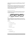
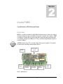
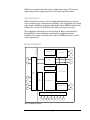
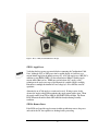
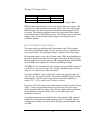
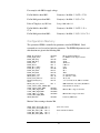
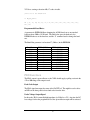
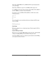
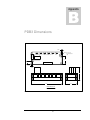
PDB3 Design Guide A N A C O N S Y S T E M S I N C D E S I G N A N D A P P L I C A T I O N C E N T E R 9 4 3 3 B E E C A V E R O A D B L D G 1 , S U I T E 1 4 0 A U S T I N , T X 7 8 7 3 3 T E L F A X 5 1 2 - 2 6 3 - 8 6 6 8 5 1 2 - 2 6 3 - 8 0 6 0 PDB3 Design Guide Revision 1.1 Copyright 2002 Anacon Systems Inc DashDrive and DigiDrive are trademarks of Anacon Systems Inc Windows is a trademark of Microsoft Corporation Table of Contents Int roduc t ion 4 Mec hanic al and Therm al 34 PDB3 Design Accelerator Kit 4 EM C a n d Sa f e t y Co m p l i a n c e 35 Before Proceeding 5 Safety 35 EMC 36 T h e I n s a n d Ou t s o f Si n g l e -Ph a s e M o t o r Co n t r o l 6 PDB 3 El e c t r i c a l Sp e c i f i c a t i o n 37 Brushed Motors 6 PDB 3 Di m e n s i o n s 38 Induction Motors 6 Re s o u r c e s 39 How Anacon Single-Phase Drives Work 7 FA Q 41 System Architecture 8 Gl o s s a r y 42 I n s i d e PDB 3 10 Overview 10 Configuration 11 Block Diagram 11 Jumpers 12 LED Status Indication 12 Fault Detection and Indication 12 Connections 13 T h e Re f e r e n c e De s i g n K i t 15 Po w e r I n t e r f a c e De s i g n 18 Considerations 18 Example 1 18 Example 2 19 Co n t r o l I n t e r f a c e De s i g n 22 Considerations 22 Serial, PWM or Analog Control 22 Example 1 23 Co n f i g u r a t i o n a n d Co m m u n i c a t i o n 2 4 Overview 24 Using a Terminal 24 Commands 25 Protocol 27 Output Voltage 27 Bus Voltage Compensation 28 Configuration Memory 29 PDO Functions 30 PDI Functions 31 Mak ing Measurem ent s 32 DC Bus Measurement 32 AC Motor Current Measurement 33 Overview Introduction Introduction to PDB3 Design Manual Single-phase Induction motors are everywhere, but until Anacon Systems created the DigiDrive family, control options were limited to poorly performing Triac based controls. Anacon’s drive technology synthesizes a true sine wave through the motor. The result is variable speed with better efficiency, quieter operation, greater range and longer life. Anacon’s Power Drive Block III (PDB3) allows Original Equipment Manufacturers to take advantage of this technology within their own products. PDB3 is a compact module containing proprietary circuits and sophisticated firmware. Creating a customized drive solution requires adding just a few external components. The PDB3 Design Guide contains detailed information on every aspect of designing with PDB3 including numerous tips to assist with product development. PDB3 Design Accelerator Kit This Manual is supplied with the PDB3 Design Accelerator Kit. Before proceeding, check that all listed items are included, and take a moment to familiarize yourself with each. PDB3 Design Guide - This document (x1) PDB3 Module – Part No. B1182 (x2) Power Interface Board (PINT) – Part No. B1201 (x1) PDB3 Configuration Kit – Part No. DD3CFG (x1) o DashDrive 2.0 for Windows 95, 98, Me, 2000 and XP o Configuration Adaptor with Cables o Instruction Manual Power Line Filters 4 o Corcom 10VK3 RFI Filter (x1) o Anacon ED-F1121-US 10 Amp EN Filter (x1) Heatsink Thermal Interface Material Insulated Speed Control Potentiometer with 3-way harness Hardware Kit (x1) A l s o r e q u i r e d (b u t n o t i n c l u d e d ) Line fuse or circuit breaker (10 Amp) Power cable Before Proceeding Power electronics involves inherent risks, both to equipment and personnel. This manual assumes that the design engineer has experience with high-voltage electronics. Incorrect use of the PDB3 can be hazardous to development staff as well as the enduser of the equipment. Throughout the manual, notes draw attention to safety related information. This is not a complete list, so the designer must research and understand electrical and mechanical issues specific to the end product. 5 Section The Ins and Outs of Single-Phase Motor Control Someimportant information onmotorselectionandoperation Motors that run directly from single-phase power can be grouped into two main categories, those that use brushes and those that don’t. Within those classifications are even more variations. Brushed Motors Brushed motors can be built with magnets (DC Brushed motor) or without (Universal motor). In either case, PDB3 is not a suitable control for these types of motors. The speed of a brushed motor is proportional to voltage, so a chopper circuit is usually the control of choice. Induction Motors Single-Phase motors without brushes are generally referred to as induction motors or squirrel cage motors. Again within this classification are several variations that have different starting methods, torque characteristics etc. The most important feature when considering using an Anacon drive is whether the induction motor contains a switching mechanism or not. Mot ors t hat c an be used w it h PDB3 and Anac on DigiDrive: Permanent Split Capacitor (PSC) Shaded Pole 6 Mot ors t hat are not rec om m ended for use w it h PDB3 or DigiDrive: Split-Phase Capacitor-Start Capacitor-Start Capacitor-Run These motors all incorporate a switching device (usually a centrifugal switch) that creates problems for variable speed control in three ways. Firstly, transient voltages occur when the switch activates, causing a fault condition on PDB3. Secondly, the starting current is typically much higher than with PSC motors, resulting in levels higher than PDB3’s 150% short-term current rating. Finally, the switch reverts to the start mode when the speed drops below about 65%, which greatly limits the useable speed range. Overall, PSC motors are the best choice for use with Anacon drives. They are widely used, readily available and give good overall performance. In pump and direct drive fan and blower applications, speed control from 20% to 110% is typical with PSC motors. How Anacon Single-Phase Drives Work The fundamental operation of PDB3 is very similar to a Three-Phase Variable Frequency Drive. The speed of an induction motor is a function of frequency, slip and the number of poles in the motor. Speed = Frequency * 120 / No. of Poles – Slip Where: Speed is in RPM, Frequency is in Hertz, Poles is number of motor poles (2, 4, 6 or 8) and Slip is also in RPM. Triac controls and other voltage controls vary the motor speed by reducing voltage to increase slip. Because Anacon drives vary frequency, slip remains almost constant over a wide speed range, resulting in control that is more precise and efficient. To vary frequency, the 50/ 60Hz AC supply is first rectified then filtered by DC Bus capacitors. Next a PWM controlled power stage switches at 18kHz to synthesize a sine wave output. When viewed with an oscilloscope, the voltage across the motor appears as a periodic sequence of fast DC pulses. Because a motor is essentially an inductor, the motor sees only the low variable frequency (i.e. 10-60Hz). This is visible in the current waveform through the motor, which is a clean sine wave. The motor windings filter the PWM voltage across the motor capacitor, so the capacitor is unaffected by variable frequency control. An important concept in variable frequency control is the Volts per Hertz curve (or VF curve). When the frequency controlling a motor is reduced, its impedance is also 7 reduced. To keep the current constant (at or below Full-Load-Amp – FLA rating) the RMS voltage to the motor must reduced. The ratio of Volts per Hertz is stored as a table in PDB3. PDB3 has a default V-F curve. Because motor characteristics vary, it is often desirable to modify the V-F curve to suit an application. For example, reducing voltage at a given frequency can improve efficiency and eliminate a mechanical resonance point. Conversely, too little voltage creates high slip and low torque. Anacon Systems’ DashDrive for Windows provides a graphical interface for making curve changes and assessing motor performance in real-time. System Architecture To simplify drive system customization, Anacon has partitioned a drive solution into three blocks. PDB3 connects between the Power Interface (PINT) block and the Control Interface (COIN) block. AC In POWER INTERFACE (PINT) PDB3 Power Drive Block CONTROL INTERFACE (COIN) Control Motor Out Figure 1 : System Block Diagram PDB3 contains highly integrated electronics, including power devices and Anacon’s proprietary microcontroller. It is a complete drive minus voltage and interface specific components. Adding PINT and COIN blocks customizes the drive system to suit the application. PDB3 Circ uit s Anacon Microcontroller Low Voltage DC Power Supply Power Devices Optoisolators Sense and control circuits Typic al PINT Circ uit s DC Bus Capacitors Power Line Filter (optional) 8 Fuse and protection circuits Terminals Typic al COIN Circ uit s Host Microcontroller (optional) RS232 Line Driver (optional) Sensor Signal Conditioning (optional) Control connectors Because PDB3 is highly integrated, a complete drive can be built by adding a single capacitor for the PINT and a potentiometer for a COIN. In practice, most applications will require some of the additional circuits listed above. The PINT and COIN circuits can often be implemented on a single circuit board. In some cases the COIN will be a board that is already present in a system. A typical example being a microprocessor based front-panel circuit board. 9 Section Inside PDB3 General Information onPDB3’sFeaturesandFunctions Overview PDB3 is a small drive module for Single-Phase Induction motors. Only a few external electronic components and a heatsink are needed for a complete drive solution. PDB3 is available in 4.0 Amp (B1181) and 6.5 Amp (B1182) current ratings and both can be used with line voltages from 100Vac to 277Vac (see Electrical Specifications, Pg36, for use above 240Vac). All PDB3 circuits except J12 are at high voltage when power is applied. Care should be taken when connecting external circuits and test Non-isolated control LEDs JP1 JP2 Jumpers DC Bus Terminals Motor Terminal AC Input Terminals Figure 2 : PDB3 Interfaces 10 Isolated Control PDB3 can be controlled with either analog or digital control signals. The two-way signals adjust the drive output frequency as well as return status information. Configuration PDB3’s internal Eeprom stores a table of configuration information for parameters such as frequency range, acceleration and alarm limits. The configuration can be edited using Anacon’s DashDrive Configuration Kit (included in the PDB3 Design Kit) and a Windows PC, or by the COIN directly, if the COIN is microprocessor based. The configuration commands are covered in Section 6. Before reading Section 6, Install DashDrive 2.0 and familiarize yourself with the configuration options. DashDrive can configure and monitor most, but not all PDB3 parameters (e.g Some control signal modes). Min 3kV Isolation 6.5mm Creapage Block Diagram L Therm al Shutdown Input Rectifier N 18V + SMPS - com Bus Voltage Sense Power Inverter Stage Isolated Interface TxD RxDi Opto Isolation Anacon Microcontroller PDI M1 M otor Current Sense PDO M2 Non-Isolated Interface 15V 5V SPD 0V REF Figure 3: PDB3 Block Diagram 11 CTL ST FLT Jumpers Option Jumper JP1 selects whether to use the factory default configuration (DEF) or customized user (USR) configuration. The position of JP1 is checked by PDB3 each time power is applied. If JP1 is in the DEF position, PDB3 writes the factory default configuration into Eeprom, overwriting whatever parameters were in there previously. The saved parameter information is retained when JP1 is in the USR position Jumper JP2 selects which V-F Curve is used when JP1 is in the DEF position. Its status is ignored at other times. JP1 and JP2 are at high voltage when power is applied. To move the jumper, first remove power and wait for the DC bus to discharge. The configuration changes will be retained, as the jumpers are only read once when power is applied. If the Eeprom gets corrupted, some values may go out of range. This can prevent PDB3 from starting. To correct this, set JP2 = DEF and cycle power. Then move JP2 to USER and reconfigure the drive. LED Status Indication Description Status Color Green Power Fault Green Red Function Pulses at 1.5Hz when output is off and no fault conditions exist. Full on when drive output is on. Indicates available AC Power Pulses fault code when drive detects a fault condition (see table below). Full off when no fault condition is present Fault Detection and Indication PDB3’s fault codes follow the same format as DigiDrive. The code is displayed as a series of flashes followed by a pause. Faults can only occur when the drive output is running. Disabling the drive output using serial commands, the Enable input, or the 05V speed input will clear faults. The appropriate method will depend on which control source is selected in the Eeprom configuration. Fault Code 2 3 4 5 6 Description Fast Current Trip (Short Circuit) Over Current Heatsink Over Temperature DC Bus Voltage too High DC Bus Voltage too Low 12 Default Setting Enabled Disabled (for now) 95Ü& Disabled Disabled Can be disabled ? No Yes No Yes Yes Connections PDB3 has three sets of connections: 1) J 1-6 High-volt age Pow er (c onnec t t o PINT) J1, J2 are AC Input Terminals J3, J4 are Motor Output Terminals J5, J6 are DC Bus Capacitor Terminals 2) J 7 Non-Isolat ed Cont rol (c onnec t t o COIN) 3) J 12 Isolat ed Cont rol (c onnec t t o COIN) Normally, only J7 or J12 is used. J12 being fully isolated is the preferred COIN connection, however it is a digital only interface. Both control connectors have DC supply outputs available for powering external COIN circuits. Refer to Electrical Specifications for voltage and current capabilities. CONTROL SIGNALS (ISOLATED) Terminal Label Description Comment J1 L AC Input J2 N AC Input J3 M1 Motor Output 1 J4 M2 Motor Output 2 J5 DC DC Bus Capacitor (+) DC Bus voltage is Vline * 1.414 J6 0V DC Bus Capacitor (-) Notes: 1. All power connections are 0.110” x 0.032” spade terminals. 2. Use AMP Part 2-520273 or equivalent fully insulated quick connector on connecting wires. 3. Wire gauge should be sized for line current (1.5 x motor current). CONTROL SIGNALS (ISOLATED) Terminal Label Description Comment J12-1 +18V +18Vdc Output J12-2 J12-3 J12-4 J12-5 J12-6 TxD RxD PDO PDI COM Serial Data Out Serial Data Input Programmable Digital Output Programmable Digital Input Common for Isolated Signals Can be used to power external circuits Open-drain output LED Cathode Refer to section 6 for functions Refer to section 6 for functions 13 Notes: 1. J12 is 6-way 0.1” polarized header. AMP Part 640456-6. 2. Mating connector is AMP/ Tyco Part 770602-6 (terminal 770666-1) CON T ROL SI GN A L S (N ON -I SOL A T ED) Terminal Label Description Comment J7-1 J7-2 J7-3 FLT STATUS CTRL J7-4 J7-5 REF 0V J7-6 J7-7 J7-8 SPD +5V +15V Fault Digital Output Status Digital Output Control Digital Input (PWM/ Enable) 0-5V Speed/ Sensor Feedback Common for Non-Isolated Signals 0-5V Speed Input Signal +5Vdc Output at 5mA +18Vdc Output at 10mA Not Implemented - Future Use Connect to speed potentiometer Can be used to power external circuits Notes: 1. J7 is 8-way 0.1” polarized header. AMP/ Tyco Part 640456-8. 2. Mating connector is AMP/ Tyco Part 770602-8 (terminal 770666-1) 3. Wire must have approved insulation for AC line voltage 14 Section The Reference Design Kit HowtoassembleandevaluatethePDB3 ReferenceDesign Kit The components in the Reference Design Kit can be assembled into a complete working drive to allow evaluation of motor performance under variable speed. The Configuration Kit (DD3CFG) allows a Windows PC to take the place of a COIN board (Control Interface). Refer to Configuration Kit documentation for instructions on software installation and operation. STEP 1 : Mount PDB3 on Heatsink. Remove the blue backing from the thermal interface material, included in the hardware kit. Apply the interface material to PDB3’s aluminum mounting plate. Next remove the clear backing from the exposed side of the thermal interface material. Position PDB3 on heatsink with the power connections in the center of the heatsink. Secure with the short 8-32 screws and washers. STEP 2: Mount PINT on Heatsink and Connect PINT Use 3 plated spacers and the long 8-32 screws to mount the PINT board on the heatsink. Six flying wires from the PINT connect to the power connections on PDB3. 0V DC AC AC M1 M2 BLACK RED BROWN BLUE WHITE YELLOW Finally connect the 3 way wire harness to J7. The two pin connector from the harness connects to J3 or J4 on the PINT board. This wiring provides a speed control potentiometer and supplies power to the in-rush control relay on the PINT. 15 Figure 4 : Photo of Fully Assembled Reference Design STEP 3: Apply Power Verify that the drive powers up correctly before connecting the Configuration Cable. Note : Although 115V or 230V power can be applied directly, it is better to use a current limited supply for the initial power up test. A DC lab supply set to 100V DC is sufficient to start PDB3’s SMPS. Set the current limit to 100mA. Standby supply current will be 50mA or less. PDB3 runs perfectly from a DC supply, so this technique can be used at any stage of development, if a suitable supply is available. Remember to multiply the nominal AC rms voltage by 1.414 to find the exact DC equivalent. Alternatively, an AC lab supply or a variac can be used. If using a variac, slowly advance the supply voltage while monitoring the supply current with a meter. When the supply reaches about 70Vac (100Vdc) the PDB3’s LEDs will light. The Power LED will remain lit and the Status LED will flash slowly indicating a standby condition. STEP 4: Remove Power If the LEDs are lit and the supply current is within specification, remove the power and wait for the DC bus capacitors to discharge before proceeding. 16 The DC bus capacitors can hold high voltages for extended periods if no current is drawn from them. PDB3’s power supply acts to discharge the capacitors in less than 30 seconds. If PDB3 is not connected, or it is otherwise non-functional, the bus capacitors may not discharge. In all situations use caution and verify that the capacitors have discharged by measuring the DC bus voltage (between 0V and DC terminals) with a meter. STEP 5: Evaluate Connect the Configuration Adaptor to J12 on the PDB3. Use the supplied straightthrough serial cable to connect the Configuration Adaptor’s 9-pin connector to a PC serial port. Install DashDrive 2.0 or susequent version, following the instructions in the DashDrive 2.0 User Manual. Connect a motor to the drive output and apply power establish a connection to PDB3. Depending on the speed input control setting, either the speed pot or DashDrive will control the motor speed. The default settings will provide a good starting point for determining optimal configuration. As a minimum, we suggest configuring the following parameters, in this order: 1) Maximum Frequency, 2) Minimum Frequency, 3) Acceleration / Deceleration, 4) Volts-Hertz Curve, 5) Boost STEP 6: Filter Evaluation Two filter samples have been provided with the Design Accelerator Kit. Metal-can filters like these, are a good starting point for filter evaluation. In the final PINT design, the filter can be implemented using descrete capacitors and inductors. The 10VK3 Filter from Corcom provides modest control of conducted emissions. The ED-F1121-US Filter (available from Anacon) meets EN50081-2 and EN50081-1 when applied correctly to a PDB3 design. Figure 5 : Reference Design with ED-F1121-US Filter Installed 17 Section Pow er Interface Design HowtodesignaPowerInterfaceBoardtocreateasingle-phasedrive Depending on the application and end-market, PINT designs can range from very simple to quite complex. Designing a PINT is really a series of design decisions and does not normally involve low-level design effort. In almost all cases the PINT will be a Through-hole technology circuit board. Considerations The following checklist covers the most common items to consider in a PINT design. Form Factor Voltage Current Line Filtering Output Filtering In-Rush Control Transient Suppression Connectors Harmonic Current Control Protection Example 1 The PINT supplied in the PDB Design Kit is an example of a typical design. Its features can be summarized using the checklist proposed above. 18 Item Form Factor Voltage Requirement Custom to fit enclosure Up to 230Vac Implementation PCB outline 400V Bus Capacitors Current Line Filtering Output Filtering In-Rush Control 6.5 Amps External Filter Module Not required Suitable for 6.5Amps 4x 220uF Capacitors None None PTC + Relay Transient Suppression MOV Connectors Easy Field installation Harmonic Current Control Not required Protection External Fuse Considerations for Design Kit PINT Example 2 Figure 6 : PINT Design with Power Line Filter for 3 Amp load 19 MOV to Earth Barrier Terminal Block None None PINT Example 2 incorporates a power line filter, MOV suppressors, a NTC thermistor for in-rush control and DC bus capacitors. Power Line Filtering A power line filter is the main method for emmisions control. By controlling conducted emmisions, the filter is also successful in controlling radiated emissions from the power supply cable. Line filters usually consists of a common-mode inductor, two X-capacitors (across the line) and two Y-capacitors (line to Earth). Most power line filters follow this format and information on filter design and component selection is widely available. Probably the most important consideration is selecting a common-mode inductor with sufficient current rating to avoid saturation. Because of the input rectifier, the power factor of an inverter is much less than the motor itself. As a rule-of-thumb, the filter should be sized for 2X the motor current. This rating applies to other components affected by current, such as the fuse and power conductors. Selecting the basic components for a filter design is straightforward. However measuring it’s effectiveness is not. Anacon recommends using a test lab and/ or filter design service for fine tuning a design. This is especially true if a regulatory standard must be met (ie. EN standards for European Union). Bus Capacitors Bus capacitor selection is important in determining the performance and reliability of the system. They are one of the few components that has a definite ‘wear-out’ characteristic. The capacitor voltage should be selected according to the highest DC bus voltage (1.414 x Vline). For 115Vac +/ - 10%, 200V capacitors are normally used. The capacitor value determines its ripple-rating and internal impedance. These factors in turn influence the stability of PDB3’s output waveform under load and the temperature (and life) of the capacitor. Cornell Dublier has a capacitor life calculator applet on their website: (www.cornell-dubillier.com) In-Rush Control When power is applied, the DC bus capacitors must charge to hundreds of volts before the drive can start. This will create a current in-rush capable of damaging the input rectifier or blowing fuses if not controlled. An in-rush control circuit adds impedance while the bus capacitors charge before assuming a low-impedance state when PDB3 runs. The peak current should be kept below 25 Amps. 20 NTC thermistors are an economical solution where the line current is less than 10 Amps. Keystone Thermometrics is a good source for additional information and parts. The PINT included with the Design Accelerator Kit uses a relay in parallel with a PTC thermistor. When power is applied the relay is open and the DC bus charges through the thermistor (a resistor could be used). When the DC bus is charged, the internal +15V power supply closes the relay which shorts out the PTC. The advantage of this method over a NTC thermistor solution, is lower temperature and better in-rush control at higher operating currents. 21 Section Control Interface Design HowtodesignaCOIN boardtocontrol PDB3 COIN designs are much more application specific than PINT designs. The simplest control interface consists of nothing more than a potentiometer for varying speed. If more than a simple interface function is required, the COIN usually incorporates a microcontroller. Considerations The following checklist covers the most common items to consider in a COIN design. Serial, PWM or Analog control Isolated or Non-Isolated User Interface Sensor Signal Conditioning Fault Diagnostics Power Source In many applications, an existing microprocessor or signal-conditioning circuit can be used for the COIN function. Serial, PWM or Analog Control Three methods are available for controlling output speed (frequency). Serial control is the most flexible as it allows bi-directional exchange of information. It does imply that the COIN is microprocessor based. Serial communications is asynchronous and can be implemented with just two control lines. The PWM input option uses a 100Hz pulse-width-modulated signal to control speed over the Fmin (0%) to Fmax (100%) range. The PWM input uses a single control line, 22 which is internally isolated and suitable for long distance signaling. A PWM signal can be generated either by a microprocessor, or by an analog circuit. Example 1 Connecting PDB3 to an external microprocessor is simplified by the internal optoisolators on PDB3. In this example PDB3 has been interfaced to a PIC16F628 microcontroller from Microchip. The COIN circuit is powered from PDB3’s +18V output through a +5V regulator. A pull-up resistor (R3) is required on the TxD output. The PIC micro’s UART is configured to 4800 baud, though faster data rates could be used if the distances are short and resistor R3 is increased. When considering remote communications, keep in mind that the CMOS logic levels are not buffered and do not offer the noise immunity of RS232 or RS485/ 422 level signals. PDI (Programmable Digital Input) and PDO (Programmable Digital Output) lines are shown connecting to the micro. These connections are normally not required, as all information is available through serial communications. In some cases PDI and PDO can be configured to reduce communications by directly signaling conditions such as Start/ Stop and Under-Voltage. Figure 7 : Interfacing PDB3 to a host Microcontroller 23 Section Configuration and Communication UsingthePDB3’sserial connection forcontrol byahost system Overview The PDB3’s serial interface is used for both configuration and control. In most cases the configuration is factory programmed using a PC running DashDrive. However, there are situations where the COIN microprocessor may need to make changes. The same communications protocol is used for both configuration and control. Simple ASCII characters pass command and data information, so a Terminal program such as Hyper-Terminal (part of Windows) can be used for testing. PDB3 applies all commands and configuration changes immediately, with the exception of a baud rate change. The new baud rate setting will be applied the next time power is cycled, assuming JP1 is set to USR. Using a Terminal Configure HyperTerminal or other terminal program to match PDB3’s communications settings. The default configuration is 9600 baud, no parity, 8 data bits and 1 stop bit (9600,n,8,1). Enter the commands as shown below, followed by a carriage return <Enter>. If the command is recognized by PDB3, it will send the appropriate response, followed by “ok” . If the command is not understood, the command it received followed by “?” will be echoed. If the command is understood, but there is a problem with the data sent with the command (i.e. checksum error), then the response will be “NOT ok” . 24 Commands V – Request PDB firmware version. V Version: 01 :00 ok U – Request an Update record from PDB3 with current parameters. U :00 02 00 00 00 00 11 00 00 00 ED; ok There are 10 data values and a checksum. The data values are: 1. 2. 3. 4. 5. 6. 7. PWM Input % ( 0 – 255 = 0 - 100%) A/ D Input ( 0 – 255 = 0 – 100%) Serial Command Input ( 0 – 255 = 0 – 100%) Calculated Setpoint (Val = Freq*2) Actual Setpoint (Val = Freq*2) Modulation Index ( 128 = 100%) State Flag – Status Byte a. Stop Bit b. Run Bit c. Boost Bit d. Boost_On Bit e. ENABLED Bit f. TEMP_ALARM Bit g. SERIAL_TIMEOUT Bit h. Unused Bit 8. Bus Voltage 9. Current 10. Checksum 0 1 2 3 4 5 6 7 The U command only returns 8 bit parameters. Use the Q command for greater resolution where applicable. E - Send back the contents of the entire EEPROM (128 locations). This block is printed in 8 lines with 16 values plus a checksum for each line. Each line begins with a header that is :Exx where the E indicates these are EEPROM values, the xx is the hex address of the first value of the line. E :E00 :E10 :E20 :E30 :E40 55 0D 80 00 05 83 19 1E 00 10 21 00 61 00 1E 64 00 5A 00 2C 32 00 00 00 3A 32 00 00 00 48 6E 00 00 00 56 00 DC 00 00 64 05 6E 00 00 72 05 FF 00 00 72 25 0F 00 0E 00 72 0A 00 00 00 72 00 00 3E 00 72 01 00 00 00 72 05 00 00 00 72 02 00 00 00 72 A6 91 5B 00 D5 ; ; ; ; ; :E50 72 05 10 1E 2C 3A 48 56 64 72 72 72 72 72 72 72 D5 ; :E60 72 72 05 0A 15 21 2C 3A 49 5F 72 72 72 72 72 72 1D ; :E70 72 72 72 05 06 0D 16 20 2B 3C 50 72 72 72 72 72 6B ; ok S – The “ S” command stores a value at a particular EEPROM location. The format of the command is Saavvcc. This command says, at EEPROM location aa, store value vv, cc is an 8-bit checksum. The checksum is computed so that the 8 bit sum of aa + vv + cc is always 0. All values must be in HEX and zero padded so that there are always 6 characters after the S command. The HEX numbers A-F must be entered in upper case. If the firmware agrees that the checksum is correct and successfully programs the value, it will respond with an “ ok” prompt. If the checksum is not correct, it will respond with “ NOT ok” . The following command programs location 30(hex) with 55(hex). S30557B ok R – Reads a value from the EEPROM. The format of the command is Raacc where aa is the EEPROM location of the value, and cc is an 8 bit checksum. The checksum is computed so that the 8 bit sum of aa + cc is always 0. All values must be in HEX and zero padded so that there are always 4 characters after the R command. The drive will respond with the value in the format of the S command as shown above. Continuing with the example above for the S command, if you then entered the following R command: R30D0 S30557B ok F – Sets the frequency of the drive. The format of the command is Fxx, where xx is the desired speed in Hertz.. Two digits must be entered. F00 will cause the drive to stop. The drive must be in the serial input mode for this command to work. F60 ok O – Sets the operating point of the drive. The format is Offmmcc, when ff is the frequency in 0.5Hz increments, mm is the modulation, and cc is a checksum. The value of cc is such that ff + mm + cc = 0. The operating point command allows operation at points that are not on the V/ F curve. Refer to information later in this section for an explanation on how to calculate modulation The example below sets the output to 50Hz 90% modulation O648C10 ok 26 Q -- Queries operating parameters from the drive. The format of the "Q" command is "Qxx" where: xx = 00 – 16 bit PWM 01 – 16 bit 0-5V 02 – 16 bit Set Speed 03 – 16 bit Actual Speed 04 – 16 bit Modulation 05 – 16 bit State Flags 06 – 16 bit Voltage 07 – 16 bit Current 08 – Motor Phase Angle The response to the query command is a 4 digit (16 bit) hexadecimal number with MSB first. Section 7 Making Measurements explains how to scale this into a real number. Protocol The commands can all be sent in simple ASCII format. The only other protocol consideration is handshaking control. Multiple command sequences and Queries can be in succession by performing a simple check. The COIN controller should always wait for the "ok" response before sending the next command. If your control waits for the "k" character, then no additional delay is needed. The ’ok’ response indicates that the command is being actioned, and that a new command may be sent, but it may not be complete. For example, the ’O’ command may still be ramping to the new frequency. If a new ’O’ command is sent it will override the previous command. With this method, several commands per second are possible with 9600 baud. Output Voltage The amplitude of the output waveform is determined by the modulation value, expressed in percent. This value comes from the V-F curve, the boost profile, or an “ O” serial command. For example, a modulation percentage of 113% sets the AC output voltage the same as the AC line input. PDB3 requires a converted number to make internal math easier. To set the V-F curve directly, or to use the “ O” command to set modulation, convert the % value as follows: Mod_Value = Modulation Percent * 1.28 + 25 27 Therefore 113% becomes AA hex Modulation % 60 82 113 Mod_Value 66 hex 82 hex AA hex Output Voltage 70Vrms 90Vrms 100Vrms Table showing output voltage vs modulation, assuming an AC supply of 100V PDB3 and other Anacon products use open loop control of the output voltage. That is, the drive is not able to monitor its own output voltage. This is due to the complex PWM waveform. The alternate approach is to monitor and compensate for the DC bus voltage. The following paragraphs describe how to implement DC Bus Voltage Compensation using an external microprocessor. The information also provides more insights on how to accurately adjust output voltage by converting from volts to modulation and back. Bus Voltage Compensation The output voltage is proportional to the 8 bit modulation value. The modulation value comes from either the internal V-F curve, or from a serial “ O” command from an external controller. The actual output voltage is a fraction of the DC Bus voltage. 0% modulation equates to zero volts AC Output voltage. 100% internal modulation is the point at which the peak value of the AC output voltage equals the DC bus voltage. Because of inherent losses in the system, the 100% internal modulation point will result in an AC RMS output voltage that is less than the AC RMS input voltage. The PDB3 does not work internally with decimal percentages (0-100%). Instead it uses 0-79 hex to represent the same scale. Sending a modulation value of 7F hex using the “ O” command gives 100% modulation. To achieve an RMS AC output voltage that is equal to the AC input voltage, the drive “ flat-tops” the output waveform. This increases the RMS voltage by adding third harmonics. Full AC output voltage requires an internal modulation of around 113%. 113% is stored in the V-F curve as AA hex. In practice, the DC bus voltage varies slightly with load current and with AC Input voltage. Voltage compensation can be used to correct the AC output voltage against variations in DC bus voltage. If the DC bus is higher than its typical value, the modulation is scaled down. If the DC bus is lower than typical, then modulation is increased. An external microprocessor can read the DC bus voltage using the “ Q06” command, calculate the error and adjust the output voltage using the “ O” command. The error calculation must take into account the effect of ‘flat-topping’ for all modulation values over 100%. 28 For example, with 100Vac supply voltage: For Int Mod less than 100% : Vout(rms) = Int Mod % * 0.972 + 17.34 For Int Mod greater than 100% : Vout(rms) = Int Mod % * 0.33 + 71.4 If the AC Supply is, say 10% low : Comp = 100 / 90 = 1.11 For Int Mod less than 100% : 17.34 Vout(rms) = Int Mod % * 0.972 * 1.11 + For Int Mod greater than 100% : Vout(rms) = Int Mod % * 0.33 * 1.11 + 71.4 Configuration Memory The operation of PDB3 is controlled by parameters stored in EEPROM. Serial commands are used to read and write the parameters. The EEPROM parameters and their locations are given in the following table. 00 EE_Programmed: 01 EE_Input_Select: 02 EE_Max_Freq: 03 EE_Min_Freq: 04 EE_Accel: 05 EE_Decel: 06 EE_Boost_Time: 07 EE_Boost_Freq: 08 EE_Start_Mod: 09 EE_End_Mod: 0A EE_Knob_Off: 0B EE_Knob_On: 0C EE_Serial_Timeout: 0D EE_Default_Freq: values 0E EE_VF_Curve_Select: 15 EE_Current_Limit_LSBDE 0xff 16 EE_Current_Limit_MSB 17 EE_VBus_High_LSB 18 EE_VBus_High_MSB 19 EE_VBus_Low_LSB 1A EE_VBus_High_MSB 1B EE_Baudrate DE 0x55 DE 1 DE 130 DE 30 DE 10 DE 5 DE 5 DE 100 DE 64 DE 128 DE 12 DE 20 DE 10 DE 191 ;EE programmed indicator ;0 = PWM, 1=0-5V input, 2=Serial ;65 Hz ;15 Hz ;10 Hz/ sec ;5 Hz/ sec ;5 Sec ;50 Hz ;50 % ;100 % ;5% (12/ 255) 0.25V ;8% (20/ 255) or 0.4V ;10 seconds ; 75% (191/ 255) about 52Hz w/ Default DE ;60Hz Weak Fan, only used by DashDrive ;Current Limit of the drive 2 DE 0xff DE 0xFF DE 0xFF DE 0xFF ;Min DC Bus voltage for the drive DE 0x07 ;baud rate (9600 baud) ;Max DC Bus voltage for the drive Monitor Values starting at location 20h. 20 EE_Num_Starts_LSB: 21 EE_Num_Starts_MSB: 22 EE_Run_Time_LSB: 23 EE_Run_Time_ISB: 24 EE_Run_Time_MSB: DE DE DE DE DE 0 0 0 0 0 ;drive start counter ; ;Drive run time in minutes ; ; 29 VF Curve starting at location 40h, 17 values in table. ;This one is the "Weak Fan" 40 EE_VF_Curve: DE 6, 8, 17, 28, 41, 55, 77, 102, 146, 146, 146, 146, 146, 146, 146, 146, 146 Programmable Baud Rates: A parameter in EEPROM allows changing the AS1101 baud rate to any standard baud rate from 1200 to 115.2k baud. The table below gives the baud rates, the EEPROM value to set the baud rate, and the “ S” command used to change the baud rate. The Baud Rate parameter is at location 27 ( 1B hex ) in the EEPROM. Baud Rate 115.2k 76.8k 57.6k 38.4k 28.8k 19.2k 14.4k 9600 4800 2400 1200 EEPROM Value 0 1 2 3 4 5 6 7 8 9 10 EEPROM Command S1B00E5 S1B01E4 S1B02E3 S1B03E2 S1B04E1 S1B05E0 S1B06DF S1B07DE S1B08DD S1B09DC S1B0ADB PDO Functions The PDO output is open-collector so the COIN should supply a pull-up resistor in the 4.7k to 100k range, if the output is used. Fault Code Output The PDO signal can output the status of the FAULT led. The might be used to drive an LED on the front panel to show fault codes from the drive. Under Voltage Output Signal In this mode, PDO is normally high-impedance (i.e. Pulled to +5V). Any time the DC bus voltage is below the programmed level, the open-collector output will be activated. 30 When Vbus is GREATER than UV_ALARM then PDO output is high-impedance (can be pulled high). When Vbus is LESS than or equal to UV_ALARM then PDO output is low. UV_ALARM is a 16 bit value at Eeprom locations 12hex (LSB) and 13hex (MSB). If the value is 0000 hex , this feature is turned off (Default). For example to set UV_ALARM to 130Vdc (0150 hex x 0.38467), then send the following commands: S12509E ok S1301EC Ok The new limit will be active immediately and the micro will update the PDO output status every 100ms. PDI Functions Enable Input PDI can be configured to act as a digital control input. When the signal is LOW, the drive is disabled. Isolated PWM Speed Control PDI can also act as an isolated 100Hz PWM speed input where 0% is OFF and 100% is full-speed. Enabling PWM speed control disables serial speed control. Note that the PWM speed input is a completely separate function from the PWMing used to generate the motor waveform. 31 Section Making Measurements Howtoscalemeasurement readingsfromPDB3 intovolts, ampsetc. DC Bus Measurement PDB3 senses the DC bus voltage with a 10 bit ADC. Firmware filters out line frequency ripple and uses the value to set Under-Voltage and Over-Voltage limits. The COIN can use the DC bus reading to calculate AC line voltage and make minor adjustments to operating points, etc. The real DC bus voltage is approximately equal to the line input voltage x 1.414 – 2.0V. This calculation can be used to estimate the AC line voltage. The error will increase when the motor is running due to sagging on the DC bus. PDB3 makes the DC bus value available as a 16 bit number using the “ Q06” serial command. Refer to Serial Commands documentation for additional details. Span 412 Span (approx line voltage) 290 ADC Resolution (10 bit) 0.4034 ADC Resolution (line voltage) 0.283 Typical error at 25degC 2.0 Worst case error at 25degC 4.9328 Worst case error at 50degC 5.9645 Worst case error at 70degC 6.7899 Drift after 1 year 0.1808 Drift after 10 years 1.8075 Note: Error limits assume no motor load 32 Vdc Vrms Vdc Vrms ±Vdc ±Vdc ±Vdc ±Vdc ±Vdc ±Vdc AC Motor Current Measurement PDB3 estimates the motor current based on the positive DC bus current. The scale factor to convert bits to amps therefore varies with the power factor of the load. Typically, 1 bit represents 10mA of RMS motor current. To maximize accuracy for an application, the scale factor can be recalculated from measurement data. The COIN can use the scale factors to calculate the actual amps. PDB3 does not have an internal scaling capability. Accuracy is approx ±10% once calibrated for an application. Averaging several readings from PDB3 can further improve accuracy. Irms = Q07 result * 0.01 33 Section Mechanical and Thermal Howtomount andheatsink PDB3 Even with an efficiency over 95%, PDB3 needs to dissipate a lot of energy when operating at full load. A good thermal management solution not only cools PDB3, but also keeps heat away from other drive components to improve system life and reliability. PDB3’s heatsinking surface is electrically isolated, so no additional insulation barrier is needed. Thermal-paste or a material such as SIL-Pad (made by Bergquist) should be applied between PDB3 and the heatsink according to the manufacturer’s specifications. No special torque-down procedure is required, but the mounting surface must be flat and even. PBD3’s base plate temperature must be kept below 90°C. If PDB3 is not adequately heatsinked, an internal thermal cut-out will activate. 34 Section EMC and Safety Compliance RecommendationsondesigningforCE, UL, FCC andotherregulatory standards The regulatory requirements for a motor control are determined by the application and the market. Expert advise is needed to determine what standards must met. Safety PDB3 is designed to UL508c and is available as a recognized component. This standard is representative of other international standards. Within UL508c are many sub-classifications that depend on environment and application. Additional components, terminals and heatsinking will be needed to meet specific requirements. Some useful information and recommendations for safety compliance: Temperature. Safety standards apply maximum operating temperature limits for components. It’s not difficult to exceed these, especially at elevated operating temperatures, so allow plenty of margin. Components such as the NTC Termistor (for In-rush current control) are designed to get very hot. Make the component leads as long as possible to keep the heat away the PCB. Using large copper areas on the PCB also helps. Heatsink temperature is normally limited to 70°C if it can be touched by the end user. Isolation. Any metal surfaces or circuits that can be touched when the circuit is powered have special isolation requirements. To address this PDB3 has 3kV isolation and 6.5mm creapage distances on J12, the isolated control connector. Extreme applications may require addition optoisolation. Classification. A mis-classification can add a lot of unecessary work and expense. A good example is the relaxed requirements for ‘Devices having Limited Ratings’ in 35 UL508c. This classification is not immediately obvious to someone unfamiliar with the specification. Warnings. A warning label can simplify a design. For example, PDB3 does not have internal overspeed control. This can be addressed by a warning statement in the nameplate. Another example is that a warning regarding the time for the DC bus to safely discharge eliminates the need for an automatic discharge circuit. EMC A complete discussion of EMC is well beyond the scope of this manual. We are able to make some suggestions and highlight pitfalls. Emmisions Meeting emissions standards is a challenge for any electrical device, and even more so for an inverter like PDB3. As always, the best approach is to keep all conductors as short as possible. In particular, mount PDB3 as close to the motor as possible. Using shielded cable designed for AC power will also help, if it is applied correctly. Emmisions from a drive using PDB3 is dominated by noise caused by the PWM switching transitions. The Anacon microprocessor and the 18kHz carrier frequency are not significant noise sources. Current Harmonics Restrictions on the line current waveshape are now in effect for most classes of products in the European Union (EN61000-3-2) and Australia. Other countries are working on similar controls. If harmonics compliance is required, additional PINT circuitry may be necessary. Specifically designed series inductors are an economical solution for currents up to 4 Amps. Higher currents may require active power factor correction. With active PFC, the PFC stage feeds the DC bus directly, eliminating the rectifier stage. Suseptibility PDB3 has an internal MOV for controlling line to line transients. Additional devices may be required in the PINT design. PDB3 has only minimal protection on control inputs. The COIN may require filters and suppressors for ESD and other transients. PDB3 incorporates a watchdog timer so it will recover after a disturbance that causes interruption in firmware execution. 36 Appendix PDB3 Electrical Specification Parameter Typical Min Max Units N ote Supply Voltage 115 85 300 Vrms Startup Supply Voltage Drop Out Supply Voltage Standby Current Standby Power Supply Frequency 70 60 80 Vrms 42 1.0 50/ 60 0.9 DC Operation over 240V requires special conformal coating – contact factory Line Voltage required for PDB3 power supply to start Low Line Voltage before PDB3 power supply enters shut-down With 115V supply Output Voltage Output Frequency Output Current Output Current Output Current Output Current - 0 1 - Isolation Voltage Creapage - 3,000 6.5 DC Voltage Output DC Supply Current Thermal Base plate Temperature Thermal Shutdown 16.5 18.0 18.5 Vdc - - 80 mA AC I N P UT 30 Vrms 1.2 400 mA Watts Hz 300 128 4.0 6 6.5 9.5 Vrms Hz Amps Amps Amps Amps MO T O R O UTP UT Continuous rating for B1181 Model 30 second rating for B1181 Model Continuous rating for B1182 Model 30 second rating for B1182 Model I SO L A T E D C O N T R O L P O R T Vac mm - - 90 ºC 95 - - ºC 37 100% Production Tested Meets UL, CSA and IEC requirements for reinforced isolation Fully isolated and available for external circuits Fully isolated and available for external circuits Appendix PDB3 Dimensions 0.150 0.173" dia M ounting Holes ISO LATED CON TRO L 0.11" POW ER CO NNECTIONS (x2) 1.075 0.425 CONTROL 0.150 1.69 Aluminum Base Plate 1.50 3.90 PDB3 Elevations Dimensions in inches 38 Appendix Resources Somehelpful websitesandpublicationsrelatedtomotorcontrol design. G E N E R A L Anacon Systems Inc. www.anaconsystems.com I N F O R M A T I O N C O M P O N E N T S Cornell Dubilier (Capacitors) www.cornell-dubillier.com Panasonic (Electolytic Capacitors, X-Y Capacitors) www.panasonic.com/ industrial/ components Evox Rifa (X-Y Capacitors) www.evox-rifa.com Renco Electronics (Common Mode Toroids) www.rencousa.com Bergquist Company (Thermal Management) www.bergquistcompany.com C O M P L I A N C E I N F O R M A T I O N Underwriters Laboratories www.ul.com UL508c Power Conversion Equipment Canadian Standards Authority (CSA) www.csa.ca C22.2 No. 14 Global Engineering Documents (for Safety and EMC documents) www.global.ihs.com 39 T E S T E Q U I P M E N T John Fluke Manufacturing www.fluke.com Fluke 41B Power Harmonics Meter 40 Appendix FAQ FrequentlyAskedQuestions Q. What versions of DashDrive can be used with PDB3 ? A. DashDrive 2.0 and subsequent releases can be used with PDB3. Q. What is the best instrument for measuring the output voltage and current ? A. We recommend a Fluke 41B Power Harmonics Analyzer. This instrument does a great job of filtering the PWM waveform and can make many useful measurements including frequency, power and distortion. Q. Can you please send me the schematic diagrams for PDB3 ? A. No. The PDB3 hardware is proprietary to Anacon Systems. Q. Does the PDB3 serial protocol support multi-drop communications ? A. No. The protocol supports point-to-point communication only. Q. How can I get assistance with my PINT and COIN design ? A. Anacon can provide design engineering consultation and services for an hourly or fixed fee. Q. My company’s control needs go beyond PDB3’s capabilities. What are my options? A. Anacon has building blocks, an advanced library of application design and experienced design staff. We develop motor control solutions quickly and affordably. Call Toll-free 1-888-456-3398 for a proposal. 41 Appendix Glossary AC Input Voltage The AC line voltage, expressed in RMS volts. AC Output Voltage (Motor Voltage) The actual output waveform of the drive is a high frequency PWM. The AC Output voltage is the RMS representation of this voltage. COIN The Control Interface circuit connects PDB3 to a control source. It can be a simple speed control potentiometer, or a more complex analog and/ or digital circuit. DC Bus Voltage The voltage across the bus capacitors, measured in DC volts. With no load, the ripple voltage on the bus will be very low. As the load current increases the ripple will also increase. Modulation % (Internal Modulation) This can be expressed either as a normal percentage value, or as a hexadecimal equivalent. 100% modulation is 7F hexadecimal. Modulation % (External Modulation) To avoid a confusing level of detail, most Anacon documentation (including DashDrive) refer to 100% modulation as being full output voltage (i.e. 115Vac in => 115Vac out). This is easier to understand, but quite different from the internal modulation percentage. 42 PDB3 Power Drive Block 3 is a compact single-phase drive module incorporating Anacon’s proprietary technology. It requires only a few external components to create a complete drive for PSC and Induction motors. PINT The Power Interface board contains DC bus capacitors and any addition components needed to interface PDB3 to the AC line and motor load. V-F Curve The V-F curve is an internal table that determines the internal modulation value for a given frequency. The table can be modified to change the AC output voltage for a given frequency. Using the ‘O’ serial command over-rides the V-F curve and sets the modulation directly. 43 44