1
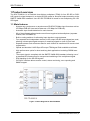
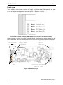
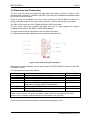
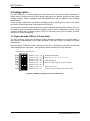
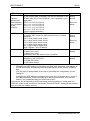
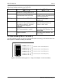
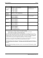
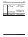
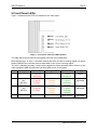
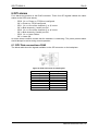
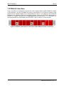
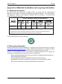
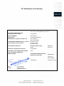
Flashlink User Manual
SDI-TD-MUX-4
4 x SD-SDI / DVB-ASI to HD-SDI
Time Division Multiplexer
network-electronics.com
Rev. 8
SDI-TD-MUX-4
Rev.8
Network Electronics ASA
P.O. Box 1020
N-3204 Sandefjord, Norway
Phone: +47 33 48 99 99
Fax: +47 33 48 99 98
Email: [email protected]
www.network-electronics.com
Support Phone: +47 90 60 99 99
Revision history
Current revision of this document is the uppermost in the table below.
Revision Replaces
Date
8
7
2008-11-10
7
6
2008-11-04
6
5
2008-04-08
5
4
3
2
4
3
2
1
2007-10-29
2007-10-08
2006-12-22
2006-11-21
1
0
0
-
2006-09-28
2006-09-21
Change description
Clarified max 35 Mbps active transport rate for DVBASI.
Corrected GPI allocation (GPI0 and GPI1 was
swapped and GPI2 and GPI3 was also swapped).
Added text in chapter 1.3 (unused input termination).
Added Declaration of Conformity.
New front page.
Added Materials Declaration and EFUP
Moved Specifications chapter to chapter 2.
New DIP-switch functionality. GYDA renamed to
GYDA-SC. Can run on a single 5V supply too.
Updated data for typical cable length
Initial revision
network-electronics.com | 2
SDI-TD-MUX-4
Rev.8
Contents
Revision history ....................................................................................... 2
1 Product overview.................................................................................. 4
1.1 Main features ........................................................................................................ 4
Front view ................................................................................................................... 5
1.2 Rear view and Connectors ................................................................................... 6
1.3 Power connection ................................................................................................. 7
1.4 Product Variants ................................................................................................... 7
2 Specifications ....................................................................................... 8
3 Configuration ........................................................................................ 9
3.1 Newer boards (FW rev 2.0 and later).................................................................... 9
3.2 Older boards (FW rev 1.x and 0.x) ..................................................................... 11
4 Operation ........................................................................................... 14
5 Front Panel LEDs ............................................................................... 15
6 GPI alarms ......................................................................................... 16
6.1 GPI/ Data connections RJ45 .............................................................................. 16
7 GYDA-SC Interface ............................................................................ 17
8 Laser safety precautions .................................................................... 18
General environmental requirements for Network Electronics equipment
.............................................................................................................. 19
Product Warranty .................................................................................. 20
Appendix A Materials declaration and recycling information .................. 21
A.1 Materials declaration .......................................................................................... 21
A.2 Recycling information ......................................................................................... 21
EC Declaration of Conformity ................................................................ 22
network-electronics.com | 3
SDI-TD-MUX-4
Rev.8
1 Product overview
The SDI-TD-MUX-4 is a Flashlink time-division multiplexer (TDM) for four SD-SDI or DVBASI inputs for signal transport in a single HD-SDI optical or electrical output according to the
SMPTE 346M-2000 standard. Use the SDI-TD-DMUX-4 board for de-multiplexing the HDSDI signal.
1.1 Main features
−
−
−
−
−
−
−
−
−
−
−
Accepts any synchronous or asynchronous SD-SDI 270 Mbps input format as well as
270 Mbps DVB-ASI (max active data rate = 35 Mbps for DVB-ASI).
Automatic input format detection for each channel.
Mix of input formats allowed and correct format regained at demultiplexer (separate
module; SDI-TD-DMUX-4).
Built-in routing switcher for allocating input signals to output streams.
Four separate and independent streams in the output HD-SDI output signal are used;
allowing uninterrupted signal transport of remaining signals on loss of input feed.
Separate stream clock reference data for each channel is transferred for remote clock
regeneration.
Optical and electrical 1.485 Gbps HD output TDM signal. Both available at all times.
High performance optics for short and long haul applications including CWDM laser
option.
The output signal is compliant with the SMPTE-346M-2000 standard, allowing use of
a standard HD infrastructure for transport and switching of the multiplexed signal.
EDH handling for the SD-SDI signals.
GYDA-SC interface allows remote control, status monitoring, error reporting and
SNMP support.
Figure 1: Block Diagram for SDI-TD-MUX-4
network-electronics.com | 4
SDI-TD-MUX-4
Rev.8
Front view
There will be a frame front covering the board and the on-board DIP-switches are then
inaccessible (cover can however be opened). The LED’s are visible through the front panel
by use of integral optical guides in the front panel, as shown in Figure 2.
Figure 2: Front Panel View with LED Indicators (only leftmost rack position shown)
Figure 3 shows a sketch of the SDI-TD-MUX-4 board. The front view will be towards the left
side of the board. The DIP switches and the LED’s are the only parts of interest for the user.
DIP switches
OFF
ON
’0’
’1’
LED
indicators
Jumper needed
for proper
operation
Optical
backplane
connector
Electrical backplane
connector with signals
and power lines
Figure 3: MUX Board Layout
network-electronics.com | 5
SDI-TD-MUX-4
Rev.8
1.2 Rear view and Connectors
The rear view of the board is towards the right side of the board, as shown in Figure 3. The
board must be mounted in a Flashlink FR-2RU-10-2 frame with a dedicated backplane board
for the SDI-TD-MUX-4 board.
Figure 4 shows the backplane rear view. Avoid inserting the SDI-TD-MUX-4 board into a
wrong backplane board, as this may cause electrical or mechanical damage to the board.
The SD1 to SD4 inputs are for 270 Mbps SD-SDI or DVB-ASI signals.
The HD output carries the electrical HD-signal with the four input signals time division
multiplexed according to the SMPTE 346M-2000 standard.
The optical and electrical outputs both carry the same HD-signal.
The GPI outputs are alarm signals for driving external alarm devices.
Figure 4: Rear view showing the backplane
Note that the same backplane can be used for both the SDI-TD-MUX-4 board and the SDITD-DMUX-4 board.
The following connectors are available:
Name
SD1
SD2
SD3
SD4
HD
Description
Connector Type
Input for 270 Mbps SD-SDI or DVB-ASI.
BNC
Input for 270 Mbps SD-SDI or DVB-ASI.
BNC
Input for 270 Mbps SD-SDI or DVB-ASI.
BNC
Input for 270 Mbps SD-SDI or DVB-ASI.
BNC
Output for 1.485 Gbps HD-SDI
BNC
(Multiplex according to SMPTE 346M-2000).
OPT
Optical output for 1.485 Gbps HD-SDI.
SC/UPC
GPI
General Purpose Interface (transistor drivers for
RJ-45
external alarm devices).
Note: There are also a number of connectors on the board itself, but none of these are
usable to the end-user. For proper operation, make sure there is a jumper in the lower
position of the connector located behind the DIP-switches (see Figure 3).
Unused inputs should be terminated to avoid alarms triggered by noise.
network-electronics.com | 6
SDI-TD-MUX-4
Rev.8
1.3 Power connection
Power is applied to the board via the backplane board, which again is plugged into the power
distribution board in the Flashlink rack.
The SDI-TD-MUX-4 board consumes slightly more than the full maximum of 3 watts from the
+5V supply and slightly more than the full maximum of 1.5 watts from the +15V supply
available at the backplane. This limits the number of boards in a rack to 8 boards plus
GYDA-SC, when using a standard single power supply.
Note that the SDI-TD-MUX-4 can also run on a single 5V supply, but then the full power of
about 4.5 watts will be drawn from the 5V supply. The board automatically adapts to sharing
the load between +5V and +15V when 15V is available.
1.4 Product Variants
SDI-TD-MUX-4
4-ch. SDI time division multiplexer, DVB-ASI compatible,
complies with SMPTE 346M-2000, electrical TDM output, ch.
swap capability.
SDI-TD-MUX-4-13T
1310nm, -7.5dBm laser + electrical interface
SDI-TD-MUX-4-15T
1550nm, 0dBm laser + electrical interface
SDI-TD-MUX-4-C1270
1270nm, 0dBm CWDM laser + electrical interface
SDI-TD-MUX-4-C1290
1290nm, 0dBm CWDM laser + electrical interface
SDI-TD-MUX-4-C1310
1310nm, 0dBm CWDM laser + electrical interface
SDI-TD-MUX-4-C1330
1330nm, 0dBm CWDM laser + electrical interface
SDI-TD-MUX-4-C1350
1350nm, 0dBm CWDM laser + electrical interface
SDI-TD-MUX-4-C1370
1370nm, 0dBm CWDM laser + electrical interface
SDI-TD-MUX-4-C1390
1390nm, 0dBm CWDM laser + electrical interface
SDI-TD-MUX-4-C1410
1410nm, 0dBm CWDM laser + electrical interface
SDI-TD-MUX-4-C1470
1470nm, 0dBm CWDM laser + electrical interface
SDI-TD-MUX-4-C1490
1490nm, 0dBm CWDM laser + electrical interface
SDI-TD-MUX-4-C1510
1510nm, 0dBm CWDM laser + electrical interface
SDI-TD-MUX-4-C1530
1530nm, 0dBm CWDM laser + electrical interface
SDI-TD-MUX-4-C1550
1550nm, 0dBm CWDM laser + electrical interface
SDI-TD-MUX-4-C1570
1570nm, 0dBm CWDM laser + electrical interface
SDI-TD-MUX-4-C1590
1590nm, 0dBm CWDM laser + electrical interface
SDI-TD-MUX-4-C1610
1610nm, 0dBm CWDM laser + electrical interface
network-electronics.com | 7
SDI-TD-MUX-4
Rev.8
2 Specifications
Electrical input
Number of inputs
Data rates
Equalisation
Impedance
Return loss
Connector
4 independent SD-SDI, DVB-ASI or SDTI
270 Mbps (Max 35 Mbps active payload for DVB-ASI)
Automatic up to 300m
75 ohm
>15dB @ 270MHz
BNC
Electrical output (standard)
Output signal
Data rate
Impedance
Return loss
Jitter (UI = Unit Interval)
Peak to peak signal level
Signal polarity
Connector
HD-SDI with TDM payload according to SMPTE 346M-2000
1485 Mbps
75 ohm
>15dB @ 1485MHz
Max. 0.2UI
0.8V ±0.1V
Non-inverting
BNC
Optical output (option)
Output signal
Transmission circuit fibre
Light source
Optical power
Optical centre wavelength
Max. wavelength drift
Jitter (UI = Unit Interval)
Connector return loss
Connector
HD-SDI, TDM payload according to SMPTE 346M-2000
Single Mode
F-P / DFB laser
-7.5dBM @ 1310nm (F-P laser), 0 dBm (DFB laser)
1310nm, 1550nm, CWDM according to ITU-T G.694.2
±20nm (F-P lasers), ±6nm (DFB lasers)
Max. 0.2UI @ 1485Mbps
better than 40dB w/ SM fibre
SC/UPC
Electrical
Temperature range
Power consumption
Control
0 to +45 °C
+5V/3.5 W, +15V/1.0W
(4.5W when running on a single +5V supply)
RS-422, GYDA-SC enabled, SNMP
Latency
Electrical and optical delay
Less than 100 us (combined through MUX and DEMUX)
In addition comes 5 us/km of fibre signal propagation time
Standards
Supported standards for electrical and optical ports:
SMPTE
SMPTE 346M-2000, SMPTE 292M, SMPTE 259M,
SMPTE 305.2M, SMPTE 297M, SMPTE RP165
DVB-ASI
EN50083-9
network-electronics.com | 8
SDI-TD-MUX-4
Rev.8
3 Configuration
The SDI-TD-MUX-4 is self-configuring in the sense that it will start working according to
default factory settings once the input signals and power are applied. Signals will be routed
straight through without swapping and SD-SDI/DVB-ASI will be detected and handled
automatically.
There are also configuration parameters available via DIP-switches in the front of the board
and via the Flashlink-protocol commands from GYDA-SC.
There are two variants of the boards. Early versions (boards with firmware revision (FW) 1.0
and earlier) have full flexibility channel swapping and no other configuration options. Later
versions (boards with firmware revision (FW) 2.0 and later) have more functions, but less
flexibility on channel swapping.
3.1 Newer boards (FW rev 2.0 and later)
The DIP switches control the channel-to-stream allocation according to the below table. It
also controls enable/bypass for the cable equalisers. See also Figure 5 for details on setting
the switches.
Note that when GYDA-SC mode is selected, there are no limitations on how the routing and
cable equalisers are controlled – as opposed to when operating from DIP-switches.
(Upper left corner of board)
OFF ON
RD0
RD1
RD2
EQ0
EQ1
EQ2
--OVR
1
2
3
4
5
6
7
8
Switch 1 (’off’ / 0)
Switch 2 (’off’ / 0)
Switch 3 (’off’ / 0)
Switch 4 (’off’ / 0)
Switch 5 (’on’ / 1)
Switch 6 (’off’ / 0)
Switch 7 (’on’ / 1)
Switch 8 (’on’ / 1)
Remote Distribution
Shown: 1=>1 , 2=>2 , 3=>3 , 4=>4
Cable Equalisers
Shown: 1 and 2 bypass, 3 and 4 enabled
Spare (not in use).
Override. Shown: DIP switch control only
Figure 5: DIP Switch Settings (see also table below)
network-electronics.com | 9
SDI-TD-MUX-4
Rev.8
DIP setting
RRR----1
Description
Comments
‘RRR’ (or RD0-2) are allowing remote control of distribution
‘000’ is
on the receiver side. Preferably, use the DIP switches on the factory
(Dashes ‘-‘
DEMUX side only or use GYDA-SC, if so is possible in your default.
indicate that
application.
these switches 000: 1=>1 2=>2 3=>3 4=>4
See note
are not related 001: 1=>1 1=>2 3=>3 4=>4
below.
to this
010: 1=>1 1=>2 3=>3 3=>4
function).
011: 1=>1 1=>2 1=>3 4=>4
1xx: 1=>1 1=>2 1=>3 1=>4
(Input to stream allocation)
---EEE-1
‘EEE’ (or EQ0-2)are controlling the cable equalisers. Leave
‘000’ is
in position ‘000’ unless you have reasons to turn off cable
factory
equalisers.
default.
000: 1=ena 2=ena 3=ena 4=ena
001: 1=byp 2=ena 3=ena 4=ena
See note
010: 1=byp 2=byp 3=ena 4=ena
below.
011: 1=byp 2=byp 3=byp 4=ena
1xx: 1=byp 2=byp 3=byp 4=byp
(byp = Bypass , ena = Enabled)
------S‘S’ is not in use.
‘0’ is factory
0: spare (not in use)
default.
1: spare (not in use)
(preferably, leave the switch in the ‘0’-position)
-------O
‘O’ is controlling whether the board is controlled by DIP‘0’ is factory
switches or from GYDA-SC.
default.
0: GYDA-SC control
1: DIP-switch control
Notes regarding distribution and cable equalisers:
− Changing the ‘RRR’ setting to something else than ‘000’ duplicates input signals on
the HD mux-stream and thereby limits the signal options at the receiver (DEMUX)
side.
− You may have to swap cables at the rear to get exactly the configuration you are
looking for.
− Changing the ‘EEE’ setting to something else than ‘000’ will bypass one or more of
the cable equalisers. This will normally give reduced performance. Only use this
feature if you understand why you would want to do it.
On power-on, the actual settings will be according to the dip-switches, except when the
GYDA-SC control mode is selected. In that case, the last GYDA-SC setting will be restored
from on-board non-volatile memory.
network-electronics.com | 10
SDI-TD-MUX-4
Rev.8
Other board settings available from GYDA-SC:
Control item
GYDA-SC mode
DIP = ‘-------0’
Laser can be turned on or off from
GYDA-SC. Factory default is ‘on’.
Under GYDA-SC control (can be
read and reset from GYDA-SC).
Laser
EDH counters
EDH flags
Can be read from GYDA-SC.
EDH masks
Can be changed from GYDA-SC.
Not stored in non-volatile memory,
so power on default is ‘all active’,
until GYDA-SC configures
otherwise.
Can be turned on/off from GYDASC. Factory default is ‘enable’.
Cable Equalizers
Channel swap
Can be controlled by GYDA-SC, all
options available.
Non-GYDA-SC mode
DIP = ‘-------1’
Laser always enabled.
Counting still active on the MUX
board (on errors), but without any
functional significance.
Flags still operating on board, but
without any functional
significance.
EDH masks remains unchanged
from last setting. Default on
power on is all active.
Cable equaliser bypass/enable
according to DIP-switches. See
above table.
Channel swap/distribution
according to DIP-switches. See
above table.
3.2 Older boards (FW rev 1.x and 0.x)
The DIP switches control the channel-to-stream allocation according to the below table. See
also Figure 5 for details on setting the switches.
(Upper left corner of board)
1
2
3
4
5
6
7
8
Switch 1 (’on’ / 1)
Switch 2 (’on’ / 1)
Switch 3 (’on’ / 1)
Switch 4 (’off’ / 0)
Switch 5 (’off’ / 0)
Switch 6 (’on’ / 1)
Switch 7 (’off’ / 0)
Switch 8 (’off’ / 0)
Stream 1 (here: from SD input 1)
Stream 2 (here: from SD input 2)
Stream 3 (here: from SD input 3)
Stream 4 (here: from SD input 4)
Figure 6: DIP Switch Settings (here: no swap; see example 1 in the below table)
network-electronics.com | 11
SDI-TD-MUX-4
DIP setting
aaxxxxxx
(X is a don’t
care bit)
xxbbxxxx
xxxxccxx
xxxxxxdd
Example 1:
00011011
Example 2:
00110110
Example 3:
00001111
Example 4:
11111111
Rev.8
Description
aa tells which of the four inputs that are
allocated to output stream 1.
00: Input 1 (SD1)
01: Input 2 (SD2)
10: Input 3 (SD3)
11: Input 4 (SD4)
bb, cc and dd are similar as aa, but for
streams 2, 3 and 4 respectively.
Comments
See Figure 6 to
understand how the bitpatterns are set.
Input 1 to stream 1.
Input 2 to stream 2.
Input 3 to stream 3.
Input 4 to stream 4.
Input 1 to stream 1.
Input 4 to stream 2.
Input 2 to stream 3.
Input 3 to stream 4.
Input 1 to stream 1.
Input 1 to stream 2.
Input 4 to stream 3.
Input 4 to stream 4.
Input 4 to stream 1.
Input 4 to stream 2.
Input 4 to stream 3.
Input 4 to stream 4.
Or controlled by GYDA.
No channel swapping.
See note below.
See note below.
Note:
The special setting in example 4 above serves dual purposes:
− Allocate inputs to output streams according to the above description.
− Allow GYDA commands to override DIP-setting.
This means that after the DIP-switches are changed from any setting to the 11111111
setting, the above allocations gets active, BUT at the same time allowing GYDA to send
commands with any other input-to-stream allocation. So, when this setting is applied to
the DIP-switches, the actual configuration depends on GYDA commands.
On power-on, the actual swap setting will be according to the dip-switches, except that
when set as in Example 4, the last GYDA command will still be active
The factory default setting will be as in example 4, with last GYDA command stored in
non-volatile memory as in example 1. This means that the default start-up is “no channel
swapping”.
All other DIP switch settings are however ‘safe’ in the sense that GYDA cannot override
these settings.
network-electronics.com | 12
SDI-TD-MUX-4
Rev.8
Other board settings available from GYDA:
Control item
Laser
GYDA mode
(DIP-sw. = ‘11111111’)
Laser can be turned on or off from
GYDA. Factory default is ‘on’.
EDH counters
Under GYDA control (can be read
and reset from GYDA).
EDH flags
Can be read from GYDA.
EDH masks
Can be changed from GYDA. Not
stored in non-volatile memory, so
power on default is ‘all active’,
until GYDA configures otherwise.
Can be turned on/off from GYDA.
Factory default is ‘enable’.
Can be controlled by GYDA, as
shown in above table.
Cable Equalizers
Channel swap
Non-GYDA mode
(any other DIP-setting)
Laser is always on. Both the
electrical and optical outputs are
active with the same signal at all
times.
Counting still active on the MUX
board (on errors), but without any
functional significance.
Flags still operating on board, but
without any functional significance.
EDH masks remains unchanged
from last setting. Default on power
on is all active.
Always enabled.
Channel swap according to DIPswitches. See above table.
network-electronics.com | 13
SDI-TD-MUX-4
Rev.8
4 Operation
The SDI-TD-MUX-4 board transfers any or all of the four 270 Mbps input signals via an
optical or electrical HD interface according to SMPTE 346M-2000. An SDI-TD-DMUX-4
board is required to reconstruct the four 270 Mbps signals, normally at a remote location and
linked via an optical fibre or an electrical coax cable.
Channel swapping is available either from DIP-switches or remotely via the standard GYDASC interface. All inputs can be either 270 Mbps SD-SDI or DVB-ASI (188 or 204 word
packets).
network-electronics.com | 14
SDI-TD-MUX-4
Rev.8
5 Front Panel LEDs
Figure 7 shows how the LEDs are located on the front panel.
Figure 7: Front Panel View with LED Indicators
The table below shows how the front panel LEDs are to be interpreted.
Note that the term “in error” in the table means that there is either a missing signal (no carrier
detect) AND/OR the reclocker has not been able to lock to the incoming signal.
The term “operating normally” means that a signal has been detected (carrier detect on the
cable equaliser) AND the reclocker has been able to lock to the signal.
Diode
1
Description
Card Status
2
SD IN 1
and
SD IN 2
Red LED
Power on,
FPGA not
configured
Both channels
(1 and 2)
in error
3
SD IN 3
and
SD IN 4
Both channels
(3 and 4)
in error
4
HD OUT
Output failure
Orange LED
Not applicable
One of the
channels
(1 or 2)
in error
One of the
channels
(3 or 4)
in error
Laser failure
Green LED
Power on and
FPGA
configured
Both channels
(1 and 2)
operating
normally
Both channels
(3 and 4)
operating
normally
Output OK and
laser working
No light
No power to
board
Not
applicable
Not
applicable
Not
applicable
network-electronics.com | 15
SDI-TD-MUX-4
Rev.8
6 GPI alarms
Four alarms are present on the RJ45 connector. These four GPI signals indicate the same
status as the LEDs (see above):
−
GPI0: On => Power on, FPGA not configured
Off => Power on, FPGA configured
− GPI1: On => One of the channels (1 or 2) in error
Off => Both channels (1 and 2) are OK
− GPI2: On => One of the channels (3 or 4) in error
Off => Both channels (3 and 4) are OK
− GPI3: On => Laser Failure
Off => Laser OK
An active alarm condition means that the transistor is conducting. The power present alarm
should always be active during normal operation.
6.1 GPI/ Data connections RJ45
The below table show the signals available on the GPI connector on the backplane.
Figure 8: RJ45 Connector for GPI Signals
RJ45 Pin Number
8
7
6
5
4
3
2
1
Description
GND
Not Used
Not Used
Not Used
GPI2
GPI3
GPI0
GPI1
network-electronics.com | 16
SDI-TD-MUX-4
Rev.8
7 GYDA-SC Interface
Figure 9 shows how GYDA-SC will present a rack equipped with an SDI-TD-MUX-4 module
in rack position 2, an SDI-TD-DMUX-4 module in rack position 6, a GYDA-SC module in rack
position 9 and a power supply unit in rack positions 10 and 11. For details on the GYDA-SC
graphical user interface or the communication protocol, refer to the GYDA-SC documents or
contact our support department at [email protected]. For information on
which parameters are controllable from GYDA-SC, refer to section 3 of this manual.
Figure 9: GYDA-SC presentation of rack with an SDI-TD-MUX-4 module in position 2
network-electronics.com | 17
SDI-TD-MUX-4
Rev.8
8 Laser safety precautions
These are guidelines to limit hazards from laser exposure.
All the available EO (including ETH100) units in the Flashlink range include a laser.
Therefore this note on laser safety should be read thoroughly.
The lasers emit light at wavelengths from 1270nm up to 1610nm. This means that the human
eye cannot see the beam, and the blink reflex cannot protect the eye. (The human eye can
see light between 400 nm to 700 nm).
A laser beam can be harmful to the human eye (depending on laser power and exposure
time). Therefore:
Be careful when connecting / disconnecting fibre pigtails (ends).
Never look directly into the pigtail of the laser/fibre.
Never use microscopes, magnifying glasses or eye loupes to look into a fibre
end.
Use laser safety goggles blocking light at 1310 nm and at 1550 nm
Instruments exist to verify light output power: Power meters, IR-cards etc.
Flashlink features:
All the laser module cards in the Flashlink product range, are Class 1 laser products
according to IEC 825-1 1993, and class I according to 21 CFR 1040.10 when used in normal
operation.
More details can be found in the user manual for the FR-2RU-10-2 frame.
Maximum output power 1:
5 mW
Operating wavelengths:
> 1270 nm
1
Max power is for safety analysis only and does not represent device performance.
network-electronics.com | 18
SDI-TD-MUX-4
Rev.8
General environmental requirements for Network Electronics
equipment
1.
2.
-
The equipment will meet the guaranteed performance specification under the following
environmental conditions:
Operating room temperature range: 0°C to 45°C
Operating relative humidity range:
up to 90% (non-condensing)
The equipment will operate without damage under the following environmental
conditions:
Temperature range:
-10°C to 55°C
Relative humidity range:
up to 95% (non-condensing)
network-electronics.com | 19
SDI-TD-MUX-4
Rev.8
Product Warranty
The warranty terms and conditions for the product(s) covered by this manual follow the
General Sales Conditions by Network Electronics ASA. These conditions are available on the
company web site of Network Electronics ASA:
www.network-electronics.com
network-electronics.com | 20
SDI-TD-MUX-4
Rev.8
Appendix A Materials declaration and recycling information
A.1 Materials declaration
For product sold into China after 1st March 2007, we comply with the “Administrative
Measure on the Control of Pollution by Electronic Information Products”. In the first stage of
this legislation, content of six hazardous materials has to be declared. The table below
shows the required information.
Toxic or hazardous substances and elements
組成名稱
Part Name
SDI-TD-MUX-4
鉛
汞
镉
六价铬
多溴联苯
多溴二苯醚
Lead Mercury Cadmium Hexavalent Polybrominated Polybrominated
Chromium
biphenyls
diphenyl ethers
(Pb)
(Hg)
(Cd)
(PBDE)
(Cr(VI))
(PBB)
O
O
O
O
O
O
O: Indicates that this toxic or hazardous substance contained in all of the homogeneous materials for
this part is below the limit requirement in SJ/T11363-2006.
X: Indicates that this toxic or hazardous substance contained in at least one of the homogeneous
materials used for this part is above the limit requirement in SJ/T11363-2006.
This is indicated by the product marking:
A.2 Recycling information
Network Electronics provides assistance to customers and recyclers through our web site
http://www.network-electronics.com. Please contact Network Electronics’ Customer Support
for assistance with recycling if this site does not show the information you require.
Where it is not possible to return the product to Network Electronics or its agents for
recycling, the following general information may be of assistance:
−
−
−
−
Before attempting disassembly, ensure the product is completely disconnected from
power and signal connections.
All major parts are marked or labelled to show their material content.
Depending on the date of manufacture, this product may contain lead in solder.
Some circuit boards may contain battery-backed memory devices.
network-electronics.com | 21
SDI-TD-MUX-4
Rev.8
EC Declaration of Conformity
MANUFACTURER
Network Electronics ASA
P.B. 1020, N-3204 SANDEFJORD, Norway
AUTHORISED REPRESENTATIVE
(Established within the EEA)
Not applicable
MODEL NUMBER(S)
SDI-TD-MUX-4
DESCRIPTION
Time Division Multiplexer
DIRECTIVES this equipment complies with
LVD 73/23/EEC
EMC 2004/108/EEC
HARMONISED STANDARDS applied in order to
verify compliance with Directive(s)
EN 55103-1:1996
EN 55103-2:1996
EN 60950-1:2006
TEST REPORTS ISSUED BY
Notified/Competent Body
Report no:
Nemko
E07381.00
TECHNICAL CONSTRUCTION FILE NO
Not applicable
YEAR WHICH THE CE-MARK WAS AFFIXED
2008
TEST AUTHORIZED SIGNATORY
MANUFACTURER
AUTHORISED REPRESENTATIVE
(Established within EEA)
Date of Issue
2008-04-08
Place of Issue
Not applicable
Name
Thomas Øhrbom
Position
Quality Manager
(authorised signature)
Sandefjord, Norway
network-electronics.com | 22