1
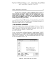
WEBENCH® Altium Connector User's Manual
SZZU007A Version: 1.1
April 7, 2014
WEBENCH Design Center
© Copyright 2013-2014 Texas Instruments Incorporated
1
Contents
Introduction ....................................................................................................... 3
Menus and Toolbar ........................................................................................... 4
WEBENCH® Altium Connector Menus and Toolbar ......................................... 4
Using WEBENCH Simulation Engine ................................................................ 7
Installing License for WEBENCH® Simulation Engine: ..................................... 7
Running WEBENCH® Simulation Engine: ........................................................ 8
WBSE Model Encryption: .................................................................................. 9
Support .............................................................................................................. 9
WEBENCH® Simulation Engine Reference Guide.......................................... 11
2
Introduction
WEBENCH® Design Environments from Texas Instruments are unique and powerful software
tools that deliver customized power, lighting, filtering, clocking and sensing designs in seconds.
These easy-to-use tools help you generate, optimize and simulate designs that conform to your
unique specifications. They allow you to make value-based tradeoffs at a design, system and
supply chain level before your design is committed to production.
WEBENCH® Altium Connector is an interface to online WEBENCH® Design Center as well as
offline WEBENCH Simulation Engine (WBSE). You can access WEBENCH® from Altium
Designer using this extension and optimize your design. You can export that design from
WEBENCH to Altium and then simulate offline in Altium. You can simulate any circuit using fast
WEBENCH Simulation Engine integrated in Altium.
This manual will take you through the steps on how to use WEBENCH® Altium Connector.
3
Menus and Toolbar
WEBENCH® Altium Connector Menus and Toolbar
•
A new WEBENCH® menu in menubar will appear.
•
You can click on any of the WEBENCH Design Tools to launch it from Altium. (e.g.
WEBENCH Designer)
4
•
WEBENCH® Simulation Engine Menus
•
•
Netlist for the project
Netlist for the document
5
•
Simulate
•
WBSE Analyses Setup
6
•
WEBENCH® Simulation Engine Toolbar
•
Mapping of toolbar icons to the function is shown in below
figure.
Using WEBENCH Simulation Engine
Installing License for WEBENCH® Simulation Engine:
•
When you run the WEBENCH simulation engine for first time on a design, it will ask for a
node license.
•
Attach the logfile showing the WBSE license not found and send an email to
[email protected] for a license. This file is needed for generating a WEBENCH® Simulation
Engine license.
•
Once license is received, rename the license file as "node_license" (if not already done)
and place it in <WEBENCH Extension Installation Directory>\WBSE.
•
Usually you will find it in c:\ProgramData\Altium\Altium Designer {2F259E6B-E4FF-4EB49ABC-063D5507D841}\Extensions\WEBENCH\WBSE\node_license
•
You are ready to use the WEBENCH® Simulation Engine.
Note: The received license file may have some extension associated with it. The license file
must be renamed to "node_license", removing any extension if present.
7
Running WEBENCH® Simulation Engine:
1. To simulate a design in WEBENCH® Simulation Engine, go to Design -> Simulate ->
WEBENCH Simulation Engine or you click on 'Run' toolbar button.
2. It will open simulation settings UI. Analysis setup window contains mainly of three parts.
1. Enable Analysis/Options: These options allow to enable/disable the required analysis.
Currently AC, DC and Transient simulations are available. Global parameters and
advanced options can also be edited here.
2. Data Collection, Viewing and Netlisting: These options enable user to control netlisting,
data saving and Sim View setup options.
3. Signal Selection: The active signals can be selected from a list of available signals.
Active signals are plotted when the simulation is running.
3. If you want to make changes to the settings, click on respective analysis name on the left
pane and edit the options.
4. If you want to specify some simulation parameter, it can be defined in the Global Parameter
options.
5. The project is ready for simulation. Click on OK to run simulation. It will start simulation and a
plot window will be opened.
8
WBSE Model Encryption:
•
WBSE Encrypted Library for the component is supported.
•
The above example is provided with your installation of this extension and can be found in
<WEBENCH Extension Installation Dir>\WBSE\Examples directory of your system.
The example uses WBSE encrypted model.
Exporting Design from WEBENCH® Designer
In order to export a design, first open a design in WEBENCH (e.g. TPS62130).
Click on CAD export button and choose Altium Designer in Simulation Export panel.
Click on Export to download simulation export file. On successful completion of export process,
9
click on download file and save the simulation xml.
Open the design in Altium using Open WEBENCH Design from WEBENCH menu bar. You can
simulate design using WEBENCH Simulation Engine.
Support
For reporting bugs or any other help regarding WEBENCH® Altium Connector please post your
queries to WEBENCH Design Center in TI E2E forum from WEBENCH Menu.
10
WEBENCH® Simulation Engine Reference Guide
Introduction to WBSE
WEBENCH® Simulation Engine [WBSE] is a general-purpose circuit simulation program that
analyzes electronic circuits using direct-method circuit simulation techniques. These techniques
provide precise waveforms for voltages, currents, and charges in the circuit.
WBSE simulates circuits containing a range of devices, including:
• Resistors
• Capacitors
• Inductors and mutual inductance
• A variety of independent and dependent voltage and current sources
• Lossy and lossless transmission lines
Range of non-linear devices include:
• Bipolar junction transistors
• Junction field-effect transistors
• MOS field-effect transistors
WBSE uses built-in models for these non-linear semiconductor devices and you need to specify
only the pertinent model parameters.
WBSE requires at least one file as input. The input file should contain the circuit description in the
form of a netlist of primitive circuit components, the models used for all non-linear devices in the
circuit, the analyses that need to be performed on the circuit, the options to be used for the
analyses, and finally the outputs that need to be saved.
11
Overview
Overview
Analyses performed by WEBENCH® Simulation Engine [WBSE] can be grouped into 3 domains:
• DC domain
These analyses compute the stable dc state of the circuit. All device parameters are computed
first. Next, WBSE performs iterations to propagate the dc values of all independent sources in the
circuit to all other nodes and devices in the circuit. Iterations continue until a steady-state is
achieved. In the steady state, voltage on nodes, charge on capacitors, flux in inductors, and
currents through resistors become constants.
DC domain analyses include:
• OP : operating point analysis
• DC : dc transfer curve analysis
• Time domain
In time domain, WBSE first computes the time=0 steady state solution. Then 'time' is increased
and the value of time-varying independent sources change. As a result, node voltages change,
capacitors charge or discharge, and currents through devices change. WBSE takes appropriately
small time-steps and re-computes the stable state. This process is repeated until the end of the
time-domain simulation.
Time domain analysis includes:
• TRAN : transient analysis
• Small-Signal Frequency domain
These analyses work on a stable operating point of the circuit. At the operating point, WBSE
generates the linearized small-signal model of the circuit. In small-signal frequency domain, the
circuit's behavior is analyzed at different real or complex frequencies.
Frequency domain analyses include:
• AC : ac analysis
The operating point for small-signal analyses can either be a stable dc solution where all
independent sources are set to their "dc" values, or it can be a converged time-point solution
during a transient analysis, where all time-varying independent sources are set to their time
values.
12
Overview: Transient Analysis
TRAN : Transient analysis
A transient analysis performs a time-domain analysis of your circuit over a specified time
interval. Before starting the transient analysis, WBSE computes the operating point of the circuit
using the time=0 values of all independent sources that have a time function. Other independent
sources get their dc values at time=0. This is an operating point analysis that results in an "initial
transient" solution of the circuit. After the time=0 solution is obtained, WBSE starts to increment
'time' in steps. The voltages of all time dependent sources are updated. Capacitive components
in the circuit are allowed to charge and discharge, and flux through inductors is allowed to
change. Currents through devices can change. WBSE recomputes the solution of the circuit at
the new time-point. It does so by starting from the previous timepoint solution. The process
repeats until time reaches the specified stop time for the transient analysis.
Time-stepping
WBSE can take a fixed-time step for the entire transient analysis. More commonly, WBSE
computes a new time-step size at every time-point. The step-size is based on circuit
characteristics, and the rate of change of voltages and currents in the circuit.
Accuracy
Accuracy parameter settings also determine the time-step size. Loser error tolerance settings will
make WBSE take bigger time-steps. This will finish the transient simulation sooner at the cost of
inaccuracies in the results. Tighter error tolerances will keep the time-steps smaller. The results
will then be more accurate at the cost of longer run times.
13
Transient Analysis Parameters
Simulation Time & Interval Parameters
TSTEP
Defines the time-step size for fixed time-step controlling methods. It may also be used as default
values of some parameters on some independent sources. An example is the rise-time of a pulse
source.
TSTART
If the waveform output of a transient analysis is not interesting from time=0 to a certain time
value, the size of the waveform files written by WBSE can be reduced by setting TSTART to the
time value from which you want to see the waveforms. This does not save simulation time,
because the transient analysis always starts from time=0.
TSTOP
Stop time value at which transient analysis stops.
TMAX
For variable time-step methods step-size can become large if there is no activity in the circuit.
Specifying TMAX will not allow WBSE to take a step-size larger than that value. The default
(1/20th of TSTOP) can be too large for oscillator circuits. For accurate results on such circuits, be
sure to set TMAX to no more than 1/20th of the period of oscillation.
TRES
Certain devices can cause discontinuous events at their output during a transient analysis.
Discontinuous events include instantaneous switching. PWL and math expression types of
controlled sources can exhibit such behavior. Truncation error becomes large when this happens,
and it can make WBSE take very small time-steps. Reducing time-step to TMIN to locate the
exact corner and recovering to larger time-steps can be inefficient. TRES allows you to set a
higher threshold than TMIN to resolve such transitions.
Usually TRES is significantly larger than TMIN.
Accuracy & Convergence Parameters
LTERATIO
Local truncation error (LTE) is the error in integration over time. This represents the difference
between the computed solution and the predicted solution derived from an extrapolation of the
solutions at the previous few time points. LTE needs to be controlled in a transient analysis to
avoid inaccuracies in results due to very large time-steps.
Tolerance for LTE, or ToleranceLTE is defined as a constant multiple of Tolerance NR:
14
LTERATIO = Tolerance LTE / Tolerance NR
RELTOL and ABSTOL parameters control the accuracy of the solution to within the specified
tolerance at any given time. This tolerance is called the Newton-Raphson tolerance, or
ToleranceNR. It is defined by the equation:
ToleranceNR = ABSTOL + RELTOL × REF
In other words, LTERATIO is defined as: To reduce LTE, while keeping error tolerance for
voltages and currents the same, you can make LTERATIO smaller. To reduce them both, you
can make RELTOL and/or ABSTOL smaller. If you make RELTOL and/or ABSTOL larger, and
want to maintain the same LTE tolerance, you will also need to decrease LTERATIO.
MAXITERS
WBSE usually takes less than 3 iterations to converge at any time point > 0. If 'MAXITERS'
iterations are reached without convergence at any time-point, the time-step size will be reduced
and convergence attempted again at an earlier time point. In other words, the transient analysis
backs up. Backups due to reaching this iteration limit usually indicates other problems in the
circuit or models.
MAX_LIMITING_ITERS
Maximum iteration allowed during transient with devices enter limiting mode, default value is 200.
UIC
This parameter tells WBSE to bypass the traditional "initial transient convergence" flow and just
use the provided "Initial Conditions" as the time=0 solution. The IT values, if specified, are
ignored. If not used carefully, 'UIC" can cause serious non-convergence problems at the first time
point of the transient analysis. This is especially true if, at the very first time point, voltages in the
circuit have sharp changes from zero or the initial conditions provided.
15
Overview: AC Analysis
AC : AC analysis
An ac analysis determines the response of a linearized small-signal model of your circuit, to the
frequency of 'ac' sources in your circuit. Typically, in an ac analysis, you sweep the frequency of
the ac sources while your circuit is biased at the same operating point. WBSE allows you to
sweep other variables as well in an ac analysis.
Prerequisites for AC analysis
To perform an ac analysis, there should be at least one independent "ac" source in the circuit. If
there are multiple "ac" sources, WBSE will write a warning but continue the simulation. The effect
will be a superposition of all the ac sources in the circuit.
16
AC Analysis Parameters
POINTS
Number of points through the AC sweep. Definition depends on TYPE of SWEEP.
SWEEP TYPE
Types of Sweep:
LINEAR - Linear. Size will be "(stop-start)/(points-1)".
DECADE - Logarithmic by octaves. Points specified are per decade.
OCTAVE - Logarithmic by decades. points specified are per octave.
START FREQ
Start value of frequency sweep.
STOP FREQ
Stop value of frequency sweep
17
Overview: DC Analysis
DC : DC analysis
A dc analysis determines a series of dc solutions of the circuit while one or more circuit variables
are swept. Originally, as the name implies, this analysis was designed to sweep the dc value of
an independent voltage or current source and watch the circuit response.
WBSE computes the dc solution at the first point of the sweep variable(s) starting from zero or
the specified initial conditions. All subsequent points of the sweeps are solved by taking the
previous solution as the initial guess. The assumption here is that the step size of the sweep is
small and so the solution will change very slightly. Two situations invalidate this assumption. First
is the case of nested sweeps when the inner loop variable switches back to its starting value
while the outer loop variable takes the next step. The second case is when the circuit switches
states very abruptly due to high gains of some circuit components. Default iteration count limits,
and step sizes can be adjusted to solve non-convergence problems that such situations can
cause.
18
DC Analysis Parameters
POINTS
Number of points through the DC sweep. Definition depends on TYPE of SWEEP.
SWEEP TYPE
Types of Sweep:
LINEAR - Linear. Size will be "(stop-start)/(points-1)".
DECADE - Logarithmic by octaves. Points specified are per decade.
OCTAVE - Logarithmic by decades. points specified are per octave.
SWEEP VARIABLE
Name of the variable to be swept.
START VALUE
Start value of sweep variable.
STOP VALUE
Stop value of sweep variable.
19
Tolerance Parameters
Tolerance parameters control the accuracy of a computed value while iterating to a converged
solution. In other words, they limit the error to within the desired tolerance for accuracy. These
parameters are optional and can be specified on all of the analyses described above. Accuracy
parameters are described in the table below.
The equation that uses these parameters to compare two values, Val1 and Val2 of a variable is:
|Val1 − Val2 | <= ABSTOL + RELTOL × min (|Val1 | , |Val2 |)
Here ABSTOL (=VABSTOL for voltages or IABSTOL for currents) is the "absolute" error
component of the error. RELTOL is the "relative" error component.
RELTOL
Default=1e-3
Relative error tolerance.
VABSTOL
Default=1e-6
Absolute voltage error tolerance.
IABSTOL
Default=1e-9
Absolute current error tolerance.
GMIN
Default=1e-12 mhos
This option sets the minimum conductance value allowed for any of the elements in your circuit. A
gmin conductance between a pair of nodes in the circuit is "nearly" an open circuit. The current
through this conductance should be several orders of magnitude smaller than other currents
through those nodes. Generally a gmin conductance should not change your simulation results. If
there are real conductances in your circuit that are close to gmin, you can reduce the value of this
option.
20
Model Convergence Options
CHECK_DCMAX
Default=true
If set to "false", this option turns off the checking of currents and voltages at a dc operating point
against the values of CURMAX (Default=1 amp) and VOLTMAX (Default=1 amp) options.
TRAN_LIMITING
Default=false
Enable device limiting during the transient, critical for behavior model or control source with
abrupt transitions.
OPTSTEP
Default=off
Enable TI proprietary optimal time-stepping algorithm (still in beta).
21
Supported Devices
List of devices that are supported by WEBENCH® Simulation Engine
•
•
•
•
•
•
•
•
•
•
•
•
•
•
•
•
•
Bipolar Junction transistor
Capacitor
Voltage-controlled voltage source
Voltage-controlled current source
Current-controlled current source
Current-controlled voltage source
Diode
Independent current source
Independent voltage source
Inductor
Mutual Inductor
Junction FET
MOSFET
Resistor
Subcircuit instantiation
Transmission line
Voltage controlled switch
22
IMPORTANT NOTICE
Texas Instruments Incorporated and its subsidiaries (TI) reserve the right to make corrections, enhancements, improvements and other
changes to its semiconductor products and services per JESD46, latest issue, and to discontinue any product or service per JESD48, latest
issue. Buyers should obtain the latest relevant information before placing orders and should verify that such information is current and
complete. All semiconductor products (also referred to herein as “components”) are sold subject to TI’s terms and conditions of sale
supplied at the time of order acknowledgment.
TI warrants performance of its components to the specifications applicable at the time of sale, in accordance with the warranty in TI’s terms
and conditions of sale of semiconductor products. Testing and other quality control techniques are used to the extent TI deems necessary
to support this warranty. Except where mandated by applicable law, testing of all parameters of each component is not necessarily
performed.
TI assumes no liability for applications assistance or the design of Buyers’ products. Buyers are responsible for their products and
applications using TI components. To minimize the risks associated with Buyers’ products and applications, Buyers should provide
adequate design and operating safeguards.
TI does not warrant or represent that any license, either express or implied, is granted under any patent right, copyright, mask work right, or
other intellectual property right relating to any combination, machine, or process in which TI components or services are used. Information
published by TI regarding third-party products or services does not constitute a license to use such products or services or a warranty or
endorsement thereof. Use of such information may require a license from a third party under the patents or other intellectual property of the
third party, or a license from TI under the patents or other intellectual property of TI.
Reproduction of significant portions of TI information in TI data books or data sheets is permissible only if reproduction is without alteration
and is accompanied by all associated warranties, conditions, limitations, and notices. TI is not responsible or liable for such altered
documentation. Information of third parties may be subject to additional restrictions.
Resale of TI components or services with statements different from or beyond the parameters stated by TI for that component or service
voids all express and any implied warranties for the associated TI component or service and is an unfair and deceptive business practice.
TI is not responsible or liable for any such statements.
Buyer acknowledges and agrees that it is solely responsible for compliance with all legal, regulatory and safety-related requirements
concerning its products, and any use of TI components in its applications, notwithstanding any applications-related information or support
that may be provided by TI. Buyer represents and agrees that it has all the necessary expertise to create and implement safeguards which
anticipate dangerous consequences of failures, monitor failures and their consequences, lessen the likelihood of failures that might cause
harm and take appropriate remedial actions. Buyer will fully indemnify TI and its representatives against any damages arising out of the use
of any TI components in safety-critical applications.
In some cases, TI components may be promoted specifically to facilitate safety-related applications. With such components, TI’s goal is to
help enable customers to design and create their own end-product solutions that meet applicable functional safety standards and
requirements. Nonetheless, such components are subject to these terms.
No TI components are authorized for use in FDA Class III (or similar life-critical medical equipment) unless authorized officers of the parties
have executed a special agreement specifically governing such use.
Only those TI components which TI has specifically designated as military grade or “enhanced plastic” are designed and intended for use in
military/aerospace applications or environments. Buyer acknowledges and agrees that any military or aerospace use of TI components
which have not been so designated is solely at the Buyer's risk, and that Buyer is solely responsible for compliance with all legal and
regulatory requirements in connection with such use.
TI has specifically designated certain components as meeting ISO/TS16949 requirements, mainly for automotive use. In any case of use of
non-designated products, TI will not be responsible for any failure to meet ISO/TS16949.
Products
Applications
Audio
www.ti.com/audio
Automotive and Transportation
www.ti.com/automotive
Amplifiers
amplifier.ti.com
Communications and Telecom
www.ti.com/communications
Data Converters
dataconverter.ti.com
Computers and Peripherals
www.ti.com/computers
DLP® Products
www.dlp.com
Consumer Electronics
www.ti.com/consumer-apps
DSP
dsp.ti.com
Energy and Lighting
www.ti.com/energy
Clocks and Timers
www.ti.com/clocks
Industrial
www.ti.com/industrial
Interface
interface.ti.com
Medical
www.ti.com/medical
Logic
logic.ti.com
Security
www.ti.com/security
Power Mgmt
power.ti.com
Space, Avionics and Defense
www.ti.com/space-avionics-defense
Microcontrollers
microcontroller.ti.com
Video and Imaging
www.ti.com/video
RFID
www.ti-rfid.com
OMAP Applications Processors
www.ti.com/omap
TI E2E Community
e2e.ti.com
Wireless Connectivity
www.ti.com/wirelessconnectivity
Mailing Address: Texas Instruments, Post Office Box 655303, Dallas, Texas 75265
Copyright © 2014, Texas Instruments Incorporated