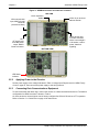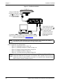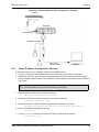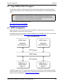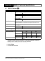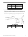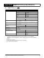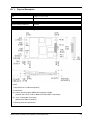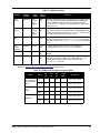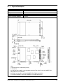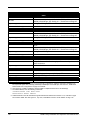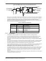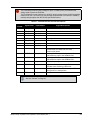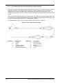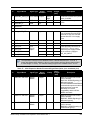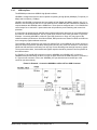
1
OEM6® Family Installation and Operation User Manual OM-20000128 Rev 7 May 2014 OEM6 Family - Installation and Operation User Manual Publication Number: Revision Level: Revision Date: OM-20000128 7 May 2014 To download the latest firmware and/or software visit: www.novatel.com/support/firmware-downloads. This manual reflects firmware version 6.500/OEM060500RN000 Warranty NovAtel® Inc. warrants that its GNSS products are free from defects in materials and workmanship, subject to the conditions set forth on our web site: www.novatel.com/products/warranty/. OEM6® Card Receivers One (1) Year FlexPak6™ One (1) Year GPS Antenna Series One (1) Year Cables and Accessories Ninety (90) Days Software Warranty One (1) Year Return Instructions To return products, refer to the instructions found under the Return Policy Tab on the warranty page: www.novatel.com/products/warranty/. Proprietary Notice Information in this document is subject to change without notice and does not represent a commitment on the part of NovAtel Inc. The software described in this document is furnished under a licence agreement or non-disclosure agreement. The software may be used or copied only in accordance with the terms of the agreement. It is against the law to copy the software on any medium except as specifically allowed in the license or non-disclosure agreement. The information contained within this manual is believed to be true and correct at the time of publication. OEM6, ALIGN, SPAN and NovAtel are registered trademarks of NovAtel Inc. FlexPak6, GLIDE, OEMV-1, OEMV-2, OEMV-3, RT-20, NovAtel CORRECT and NovAtel Connect are trademarks of NovAtel Inc. All other brand names are trademarks of their respective holders. Manufactured and protected under U.S. patents. #5,101,416 #5,390,207 #5,414,729 #5,495,499 #5,736,961 #5,809,064 #6,184,822 B1 #6,243,409 B1 #6,445,354 B1 #6,608,998 B1 #6,664,923 B1 #7,738,536 © Copyright 2014 NovAtel Inc. All rights reserved. Unpublished rights reserved under International copyright laws. 2 OEM6 Family Installation and Operation User Manual Rev 7 Table of Contents Notices 10 Customer Support 14 1 Introduction 15 1.1 Overview of the OEM6 Family of Cards and Enclosures ............................................................... 15 1.1.1 OEM6 Family Receiver Cards ..............................................................................................15 1.1.2 OEM6 Receiver Enclosure ................................................................................................... 15 1.2 Related Documents and Information..............................................................................................15 1.2.1 OEM615 Receiver ................................................................................................................ 15 1.2.2 OEM617D Receiver.............................................................................................................. 16 1.2.3 OEM628 Receiver ................................................................................................................ 16 1.2.4 OEM638 Receiver ................................................................................................................ 17 1.3 OEM6 Receiver System Overview................................................................................................. 18 1.3.1 OEM6 Family Card ............................................................................................................... 19 1.3.2 Enclosure.............................................................................................................................. 19 1.3.3 GNSS Antenna ..................................................................................................................... 20 1.3.4 Power Supply ....................................................................................................................... 20 1.3.5 Optional External Frequency Reference .............................................................................. 20 1.3.6 Data Communications Equipment ........................................................................................ 20 1.3.7 Onboard Memory ................................................................................................................. 20 1.4 OEM6 Enclosure ............................................................................................................................ 20 1.4.1 FlexPak6............................................................................................................................... 21 2 Installation OEM6 Family Cards 22 2.1 Shipping Box .................................................................................................................................. 22 2.2 Additional Equipment Required...................................................................................................... 22 2.3 Selecting a GNSS Antenna............................................................................................................ 22 2.3.1 Choosing a Coaxial Cable .................................................................................................... 23 2.3.2 Mounting the GNSS Antenna ............................................................................................... 23 2.3.3 Connecting the Antenna to the Receiver.............................................................................. 24 2.4 Power Supply Requirements.......................................................................................................... 24 2.5 Card Installation Overview ............................................................................................................. 25 2.5.1 Installing an OEM6 Family Card with Wiring Harness and Enclosure .................................. 26 2.5.2 Applying Power to the Receiver ...........................................................................................30 2.5.3 Connecting Data Communications Equipment ..................................................................... 30 2.6 OEM638 Card Security ................................................................................................................. 35 2.6.1 Administration Password ...................................................................................................... 35 2.6.2 FTP Server and ICOM Port ................................................................................................. 35 2.7 Installing NovAtel PC Utilities......................................................................................................... 35 3 Installation FlexPak6 36 3.1 Shipping Box .................................................................................................................................. 36 3.2 Additional Equipment Required...................................................................................................... 36 3.3 Selecting a GNSS Antenna............................................................................................................ 36 3.3.1 Choosing a Coaxial Cable .................................................................................................... 37 3.3.2 Mounting the GNSS Antenna ............................................................................................... 37 3.3.3 FlexPak6 Alternative Power Source ..................................................................................... 39 3.3.4 Battery Backup ..................................................................................................................... 40 3.3.5 FlexPak6 Status Indicators and Connector Labels............................................................... 40 3.4 Installing NovAtel PC Utilities......................................................................................................... 41 4 Operation OEM6 Cards and Enclosure 42 4.1 Communications with the Receiver................................................................................................ 42 OEM6 Family Installation and Operation User Manual Rev 7 3 Table of Contents 4.1.1 Serial Ports........................................................................................................................... 43 4.1.2 Communicating with a Remote Terminal ............................................................................. 44 4.1.3 Communicating with a Computer ......................................................................................... 44 4.2 Getting Started .............................................................................................................................. 44 4.2.1 Starting the Receiver............................................................................................................ 45 4.2.2 Communicating with the Receiver Using NovAtel Connect ................................................. 45 4.3 Transmitting and Receiving Corrections........................................................................................ 47 4.3.1 Base Station Configuration .................................................................................................. 48 4.3.2 Rover Station Configuration ................................................................................................. 49 4.3.3 ALIGN® Heading Master and Remote Configurations ......................................................... 50 4.3.4 PDP and GLIDE™ Configurations ........................................................................................ 51 4.4 Steadyline...................................................................................................................................... 51 4.4.1 Maintain................................................................................................................................ 51 4.4.2 Transition ............................................................................................................................. 52 4.4.3 Prefer Accuracy.................................................................................................................... 52 4.4.4 UAL ...................................................................................................................................... 53 4.5 Configuration Notes....................................................................................................................... 54 4.5.1 Enabling SBAS Positioning .................................................................................................. 55 4.5.2 Enabling L-Band................................................................................................................... 55 4.6 Transferring Time Between Receivers .......................................................................................... 57 4.6.1 GPS to Receiver Time Synchronization............................................................................... 57 4.6.2 Time Definitions ................................................................................................................... 58 4.6.3 Procedures to Transfer Time ............................................................................................... 59 4.7 Additional Features and Information (Card and Enclosure) .......................................................... 62 4.7.1 Universal Serial Bus (USB) .................................................................................................. 62 4.7.2 CAN Bus .............................................................................................................................. 63 4.7.3 Strobes................................................................................................................................. 63 4.7.4 Status Indicator .................................................................................................................... 64 4.7.5 External Oscillator ................................................................................................................ 64 4.7.6 Antenna LNA Power............................................................................................................. 64 4.7.7 Ethernet................................................................................................................................ 65 4.8 Logging and Retrieving Data Overview ......................................................................................... 65 4.8.1 Onboard Memory ................................................................................................................. 66 4.8.2 Remote Logging Initiation .................................................................................................... 66 4.8.3 Manual Retrieval of Logged Data......................................................................................... 66 4.8.4 Remote Retrieval of Logged Data........................................................................................ 66 4.8.5 Naming Logs ........................................................................................................................ 66 4.8.6 Manual Log File Naming ...................................................................................................... 67 4.8.7 Stop Logging ........................................................................................................................ 67 4.8.8 Reading Data and Post-Processing ..................................................................................... 67 4.8.9 Pass-Through Logging......................................................................................................... 67 5 Built-In Status Tests 68 5.1 Overview........................................................................................................................................ 68 5.2 Receiver Status Word.................................................................................................................... 68 5.3 Error Strobe Signal ........................................................................................................................ 69 5.4 RXSTATUSEVENT Log ................................................................................................................ 69 5.5 RXSTATUS Log ............................................................................................................................ 69 5.5.1 Overview .............................................................................................................................. 69 5.5.2 Error Word............................................................................................................................ 70 5.5.3 Status Code Arrays .............................................................................................................. 70 5.5.4 Receiver Status Code .......................................................................................................... 71 5.5.5 Auxiliary Status Codes ......................................................................................................... 71 5.5.6 Set and Clear Mask for all Status Code Arrays.................................................................... 71 5.6 Status LED .................................................................................................................................... 71 4 OEM6 Family Installation and Operation User Manual Rev 7 Table of Contents 6 Ethernet Configuration 73 6.1 Required Hardware ........................................................................................................................ 73 6.2 Static IP Address Configuration ..................................................................................................... 73 6.2.1 Static IP Address Configuration—Receiver .......................................................................... 75 6.2.2 Static IP Address Configuration—Windows XP with SP3 ....................................................76 6.2.3 Static IP Address Configuration—Windows 7 ...................................................................... 76 6.2.4 Confirming Ethernet Setup ................................................................................................... 78 6.3 Dynamic IP Address Configuration ................................................................................................ 78 6.4 Base/Rover Configuration through Ethernet Connectivity.............................................................. 81 6.5 Large COM Port Data Throughput ................................................................................................. 83 6.6 NTRIP Configuration ...................................................................................................................... 83 7 Troubleshooting 85 7.1 Examining the RXSTATUS Log ..................................................................................................... 86 7.2 Examining the AUX1 Status Word ................................................................................................. 88 8 NovAtel Firmware and Software 89 8.1 Firmware Updates and Model Upgrades ....................................................................................... 89 8.1.1 Firmware Updates ................................................................................................................ 89 8.1.2 Model Upgrades ................................................................................................................... 90 8.2 Authorization Code......................................................................................................................... 90 8.3 Updating or Upgrading Using the WinLoad Utility.......................................................................... 91 8.3.1 Transferring Firmware Files.................................................................................................. 91 8.3.2 Using the WinLoad Utility ..................................................................................................... 92 8.4 Updating Using SoftLoad Commands............................................................................................ 93 8.4.1 SoftLoad Commands and Logs ............................................................................................ 93 8.4.2 Working With S-Records ...................................................................................................... 94 8.4.3 Sending Firmware Data........................................................................................................ 95 8.4.4 SoftLoad Update Method...................................................................................................... 96 8.4.5 Firmware Update Using FTP or USB Mass Storage Device ................................................ 98 8.4.6 SoftLoad Direct Commands and Logs.................................................................................. 98 8.4.7 SoftLoad Direct Update Method ........................................................................................... 98 8.4.8 SoftLoad Errors .................................................................................................................... 99 8.5 Upgrading Using the AUTH Command .......................................................................................... 99 8.5.1 Upgrade Procedure .............................................................................................................. 99 A OEM615 Technical Specifications 100 OEM615 Receiver ...........................................................................................................................100 Physical Description ...................................................................................................................101 Logic-Level I/O ...........................................................................................................................109 CAN Interface .............................................................................................................................110 USB Interface .............................................................................................................................111 B OEM617D Technical Specifications 112 OEM617D Receiver .........................................................................................................................112 Physical Description ...................................................................................................................113 Logic-Level I/O ...........................................................................................................................119 CAN Interface .............................................................................................................................120 USB Interface .............................................................................................................................121 C OEM628 Technical Specifications 122 OEM628 Receiver ............................................................................................................................122 Physical Description ...................................................................................................................123 CMOS Level I/O .........................................................................................................................131 CAN Interface .............................................................................................................................132 USB Interface .............................................................................................................................133 OEM6 Family Installation and Operation User Manual Rev 7 5 Table of Contents Ethernet Port .............................................................................................................................. 134 D FlexPak6 Technical Specifications 137 FlexPak6 .......................................................................................................................................... 137 FlexPak6 Cables ........................................................................................................................ 140 E OEM638 Technical Specifications 145 OEM638 Receiver ........................................................................................................................... 145 Physical Description ................................................................................................................... 146 Power Supply ............................................................................................................................. 163 Antenna Power Output ............................................................................................................... 163 Logic-Level I/O ........................................................................................................................... 163 Communication Ports ................................................................................................................. 165 CAN Interfaces ........................................................................................................................... 165 USB Interfaces ........................................................................................................................... 167 Ethernet Port .............................................................................................................................. 168 System Performance ................................................................................................................. 170 F Accessories and Replacement Parts 171 FlexPak6 ........................................................................................................................................... 171 Accessories ...................................................................................................................................... 171 Manufacturers’ Part Numbers ........................................................................................................... 172 G Electrostatic Discharge (ESD) Practices 173 Overview ........................................................................................................................................... 173 Handling ESD Sensitive Devices ...................................................................................................... 173 Prime Static Accumulators ............................................................................................................... 174 Handling Printed Circuit Boards ....................................................................................................... 174 6 OEM6 Family Installation and Operation User Manual Rev 7 Tables 1 2 3 4 5 6 7 8 9 10 11 12 13 14 15 16 17 18 19 20 21 22 23 24 25 26 27 28 29 30 31 32 33 34 35 36 37 38 39 40 41 42 43 44 FlexPak6 Features ............................................................................................................................... 21 Voltage Input Requirement for OEM6 Family Cards ............................................................................ 25 OEM6 Card Default Serial Port Configurations .................................................................................... 31 Fuse/Holder Recommendations-12 V System ..................................................................................... 39 FlexPak6 Status Indicators and Connector Labels ............................................................................... 40 FlexPak6 Default Serial Port Configuration .......................................................................................... 41 Serial Ports Supported ......................................................................................................................... 43 Available USB Signals on Receivers .................................................................................................... 62 Troubleshooting Based on Symptoms .................................................................................................. 85 Resolving a Receiver Error Word ......................................................................................................... 86 Resolving an Error in the Receiver Status Word .................................................................................. 87 Resolving an Error in the AUX1 Status Word ....................................................................................... 88 OEM615 Strobes ................................................................................................................................ 107 OEM615 Strobe Electrical Specification ............................................................................................. 107 Bill of Materials (critical components) ................................................................................................. 110 Bill of Materials (critical components) ................................................................................................. 111 Bill of Materials ................................................................................................................................... 111 OEM617D Strobes ............................................................................................................................. 117 OEM617D Strobe Electrical Specification .......................................................................................... 117 Bill of Materials (critical components) ................................................................................................. 120 Bill of Materials (critical components) ................................................................................................. 121 Bill of Materials ................................................................................................................................... 121 OEM628 Strobes ................................................................................................................................ 129 OEM628 Strobe Electrical Specifications ........................................................................................... 129 ESD Critical Components ................................................................................................................... 132 CAN Critical Components ................................................................................................................... 133 USB Critical Components ................................................................................................................... 134 Ethernet Transformer Characteristics ................................................................................................. 136 Bill of Materials (critical components) ................................................................................................. 136 FlexPak6 Port Pin-Out Descriptions .................................................................................................. 138 FlexPak6 I/O Port Pin-Out Descriptions ............................................................................................. 139 I/O Breakout Cable Wiring. ................................................................................................................. 140 I/O Strobe Port Cable Wiring .............................................................................................................. 141 Null Modem Cable Wiring ................................................................................................................... 143 OEM638 Strobes ................................................................................................................................ 151 OEM638 Strobe Electrical Specifications ........................................................................................... 152 J4101 Expansion Header Pinout and Signal Description (even numbered pins) ............................... 159 3.3V CMOS Electrical Characteristics (-40 to 85°C) .......................................................................... 162 Bill of Materials (critical components) ................................................................................................. 164 Bill of Materials (critical components) ................................................................................................. 166 Bill of Materials ................................................................................................................................... 168 Recommended Ethernet Transformer Characteristics ....................................................................... 170 Bill of Materials (Critical Components Only) ....................................................................................... 170 Static-Accumulating Materials ............................................................................................................ 174 OEM6 Family Installation and Operation User Manual Rev 7 7 Figures 1 2 3 4 5 6 7 8 9 10 11 12 13 14 15 16 17 18 1 2 3 4 5 19 20 21 22 23 24 25 26 27 28 29 30 31 32 33 34 35 36 37 38 39 40 41 42 43 44 45 46 47 48 49 OEM615 Receiver Board ...................................................................................................................... 16 OEM617D Receiver Board ................................................................................................................... 16 OEM628 Receiver Board ...................................................................................................................... 17 OEM638 Receiver Board ...................................................................................................................... 17 OEM615, OEM617D and OEM628 Receiver System .......................................................................... 18 OEM638 Receiver System ................................................................................................................... 19 FlexPak6 ............................................................................................................................................... 21 OEM615 Connector and Indicator Locations ........................................................................................ 28 OEM617D Connectors and Indicators .................................................................................................. 29 OEM628 Connector and Indicator Locations ........................................................................................ 29 OEM638 Connector and Indicator Locations ........................................................................................ 30 COM3 and USB Multiplexed on OEM615 and OEM617D .................................................................... 32 OEM628 COM3 Multiplexed with EVENT2 and USERGPIO ............................................................... 33 OEM638 Multiplexed Pin Options ......................................................................................................... 34 FlexPak6 Installation ............................................................................................................................ 38 FlexPak6 Connectors ........................................................................................................................... 40 Basic OEM6 Family Card Connection Interfaces (example) ................................................................ 42 Basic Differential Setup ........................................................................................................................ 47 Steadyline Maintain .............................................................................................................................. 52 Steadyline Transition ............................................................................................................................ 52 Steadyline Prefer Accuracy .................................................................................................................. 52 Steadyline UAL- Warning Limit Example .............................................................................................. 53 Steadyline UAL - Out of Bounds Example ............................................................................................ 54 Transfer COARSE Time from Fine Clock to Cold Clock Receiver ....................................................... 59 Transfer FINE Time from Fine Clock to Cold Clock Receiver .............................................................. 60 Transfer FINE Time from Fine Clock to Warm Clock Receiver ............................................................ 61 1 PPS Alignment .................................................................................................................................. 61 Location of Receiver Status Word ........................................................................................................ 69 Reading the Bits in the Receiver Status Word ..................................................................................... 69 Location of Receiver Error Word .......................................................................................................... 70 Reading the Bits in the Receiver Error Word ........................................................................................ 70 Status LED Flash Sequence Example ................................................................................................. 72 Cross-Over Ethernet Cable Configuration—OEM628 and OEM638 .................................................... 74 Cross-Over Ethernet Cable Configuration—FlexPak6 ......................................................................... 75 Dynamic IP Address Configuration through a DHCP Server—OEM628 and OEM638 ........................ 79 Dynamic IP Address Configuration through a DHCP Server—FlexPak6 ............................................. 79 Base/Rover Ethernet Setup—OEM628 and OEM638 .......................................................................... 81 Base/Rover Ethernet Setup—FlexPak6 ............................................................................................... 82 NTRIP System ...................................................................................................................................... 83 WinLoad’s Open Window ..................................................................................................................... 92 Open File in WinLoad ........................................................................................................................... 92 COM Port Setup ................................................................................................................................... 92 Searching for Card ............................................................................................................................... 93 Authorization Code Window ................................................................................................................. 93 Upgrade Process Complete ................................................................................................................. 93 OEM615 Board Dimensions ............................................................................................................... 101 OEM615 Keep-Out Zone .................................................................................................................... 102 OEM615V Board Dimensions ............................................................................................................. 103 OEM615V Keep-Out Zone ................................................................................................................. 104 Top-view, P1101 Main Connector 20-Pin Header .............................................................................. 108 OEM615 ESD Protection for EVENT and PPS Strobes Schematic ................................................... 109 OEM615 PV LED Drive Buffer Schematic .......................................................................................... 110 OEM615 CAN Transceiver Implementation Schematic ...................................................................... 110 OEM615 USB Implementation Schematic .......................................................................................... 111 OEM6 Family Installation and Operation User Manual Rev 7 8 Table of Contents 50 51 52 53 54 55 56 57 58 59 60 61 62 63 64 65 66 67 68 69 70 71 72 73 74 75 76 77 78 79 80 81 82 83 84 85 OEM617D Board Dimensions ............................................................................................................ 113 OEM617D Keep-Out Zone ................................................................................................................. 114 Top-view, P1101 Main Connector 20-Pin Header .............................................................................. 118 OEM617D ESD Protection for EVENT and PPS Strobes Schematic ................................................. 119 OEM617D PV LED Drive Buffer Schematic ....................................................................................... 120 OEM617D CAN Transceiver Implementation Schematic ................................................................... 120 OEM617D USB Implementation Schematic ....................................................................................... 121 OEM628 Board Dimensions ............................................................................................................... 123 OEM628 Keep-Out Zone .................................................................................................................... 124 OEM628V Board Dimensions ............................................................................................................. 125 OEM628V Keep-Out Zone ................................................................................................................. 126 Top-view, P1500 Main Connector 24-Pin Header .............................................................................. 130 Top-view, P1502 Expansion 16-Pin Header ....................................................................................... 131 OEM628 ESD Protection for EVENT and PPS Strobes Schematic ................................................... 132 OEM628 LED Drive Buffer for ERROR and PV Signals Schematic ................................................... 132 OEM628 CAN Transceiver Implementation Schematic ...................................................................... 133 OEM628 USB Implementation Schematic .......................................................................................... 134 Ethernet Reference Schematic .......................................................................................................... 135 Ethernet LED Buffer Schematic .......................................................................................................... 136 FlexPak6 Dimensions ......................................................................................................................... 138 I/O Breakout Cable ............................................................................................................................. 140 I/O DB-HD15 Strobe Port Cable ......................................................................................................... 141 Straight Through Serial Cable ............................................................................................................ 142 Null Modem Cable .............................................................................................................................. 143 12 V Power Accessory Cable ............................................................................................................. 144 OEM638 Dimensions .......................................................................................................................... 146 OEM638 and OEM638V Keep-Out Zone ........................................................................................... 147 J4001 Main Header Pinout and Signal Description ............................................................................ 153 J3201 Ethernet Header Pinout and Signal Description ...................................................................... 156 J4101 Expansion Header Pinout and Signal Description (odd numbered pins) ................................. 157 Example - ESD Protection for Strobes (optional buffering for PPS) ................................................... 164 Example - LED Drive Buffer for PV and ERROR Signals ................................................................... 164 Example - CAN Protection and Filtering Circuit .................................................................................. 166 Example - Connecting HSUSB0 to a Micro-B Type USB Connector ................................................. 167 Example – Connecting HSUSB1 or HSUSB2 to a Micro-AB Type USB Connector ........................... 168 Example - Ethernet Reference Schematic ......................................................................................... 169 OEM6 Family Installation and Operation User Manual Rev 7 9 Notices The following notices apply, as appropriate, to the OEM6 family products including the OEM615, OEM617D, OEM628 and OEM638 as well as the FlexPak6. Changes or modifications to this equipment, not expressly approved by NovAtel Inc., could result in violation of FCC, Industry Canada and CE Marking rules and void the user’s authority to operate this equipment. FCC Notices This device complies with part 15 of the FCC Rules. Operation is subject to the following two conditions: (1) this device may not cause harmful interference, and (2) this device must accept any interference received, including interference that may cause undesired operation. The FlexPak6 has been tested and found to comply with the radiated and conducted emission limits for a Class B digital device. The Class B limits are designed to provide reasonable protection against harmful interference in a residential installation. The equipment listed generates, uses, and can radiate radio frequency energy and, if not installed and used in accordance with the instructions, may cause harmful interference to radio communications. However, there is no guarantee that interference will not occur in a particular installation. If this equipment does cause harmful interference to radio or television reception, which can be determined by turning the equipment off and on, the user is encouraged to try to correct the interference by one or more of the following measures: • Reorient or relocate the receiving antenna • Increase the separation between the equipment and the receiver • Connect the equipment to an outlet on a circuit different from that to which the receiver is connected • Consult the dealer or an experienced radio/TV technician for help To maintain compliance with the limits of a Class B digital device, you must use properly shielded interface cables (such as Belden #9539 or equivalent) when using the serial data ports, and double-shielded cables (such as Belden #9945 or equivalent) when using the I/O strobe port. Industry Canada FlexPak6 Class B digital apparatus comply with Canadian ICES-003. FlexPak6 appareil numérique de la classe B est conforme à la norme NMB-003 du Canada. CE Marking The FlexPak6 carries the CE mark. Emissions OEM6 family products have been designed and tested to meet regulatory emission limits. Emission levels may be higher for OEM6 family card level operation than for integrated enclosure level products, like the FlexPak6, using an OEM6 family card. The OEM615, 628 and 638 cards emission status is Class B. The OEM617D is Class A. 10 OEM6 Family Installation and Operation User Manual Rev 7 Notices WEEE If you purchased your OEM6 family product in Europe, please return it to your dealer or supplier at the end of life. The objectives of the European Community's environment policy are, in particular, to preserve, protect and improve the quality of the environment, protect human health and utilise natural resources prudently and rationally. Sustainable development advocates the reduction of wasteful consumption of natural resources and the prevention of pollution. Waste Electrical and Electronic Equipment (WEEE) is a regulated area. Where the generation of waste cannot be avoided, it should be reused or recovered for its material or energy. WEEE products may be recognized by their wheeled bin label ( ). 1 RoHS The OEM6 family and FlexPak6 are compliant with the European Union (EU) Restriction of Hazardous Substances (RoHS) Directive 2011/65/EU. REACH NovAtel strives to comply with the EU Directive EC 1907/2006 on chemicals and their safe use as per the Registration, Evaluation, Authorization and Restriction of Chemical substances (REACH) for its products, including the OEM6 family products. Since REACH SVHC lists are updated occasionally, please contact NovAtel Customer Support if you require further information. Ethernet Port The Ethernet ports are Safety Extra Low Voltage (SELV) circuits only and are suitable for connection within a building only. Do not connect them to Telephone Network Voltage (TNV) circuits. Lightning Protection Installation and Grounding Procedure What is the hazard? A lightning strike into the ground causes an increase in the earth's potential which results in a high voltage potential between the center conductor and shield of the coaxial cable. This high voltage develops because the voltage surge induced onto the center conductor lags in time behind the voltage surge induced onto the shield. Hazard Impact A lightning strike causes the ground potential in the area to rise to dangerous levels resulting in harm to personnel or destruction of electronic equipment in an unprotected environment. It also conducts a portion of the strike energy down the inner conductor of the coax cable to the connected equipment. Only qualified personnel, such as electricians mandated by the governing body in the country of installation, may install lightning protection devices. Actions to Mitigate Lightning Hazards 1. Do not install antennas or antenna coaxial cables outside the building during a lightning storm. 2. It is not possible to avoid over voltages caused by lightning, but a lightning protection device may be used to shunt a large portion of the transient energy to the building ground, reducing the over voltage condition as quickly as possible. 3. Primary lightning protection must be provided by the operator/customer according to local building codes as part of the extra building installation. 1.See http://www.novatel.com/products/weee-and-rohs/ for more information. OEM6 Family Installation and Operation User Manual Rev 7 11 Notices 4. To ensure compliance with clause 7 "Connection to Cable Distribution Systems" of EN 60950-1, Safety for Information Technology Equipment, a secondary lightning protection device must be used for in-building equipment installations with external antennas. The following device has been approved by NovAtel Inc.: Polyphaser - Surge Arrestor DGXZ+24NFNF-A If this device is not chosen as the primary lightning protection device, the device chosen must meet the following requirements: • UL listed, or equivalent, in country of installation (for example, TUV, VDE and so on) for lightning surge protection • The primary device must be capable of limiting an incoming surge to 10 kV 5. The shield of the coaxial cable entering the building should be connected at a grounding plate at the building's entrance. The lightning protection devices should have their chassis grounded to the same ground near to the building's entrance. 6. The primary and secondary lightning protections should be as close to the building's entrance as possible. Where feasible, mount onto the grounding plate itself (refer to the figure below). 4 6 3 1 2 5 5 5 5 Ref # 1 2 3 12 Description Primary lightning protection device Secondary lightning protection device External antenna Ref # 4 5 6 Description GNSS Receiver To ground Grounding plate or grounding point at the building’s entrance OEM6 Family Installation and Operation User Manual Rev 7 Notices Acceptable choices for earth grounds, for central buildings, are: • Grounded interior metal cold water pipe within five feet (1.5 m) of the point where it enters the building • Grounded metallic service raceway • Grounded electrical service equipment enclosure • Eight-foot grounding rod driven into the ground (only if bonded to the central building ground by #6, or heavier, bonding wire) These installation instructions are the minimum requirements for receiver and antenna installations. Where applicable, follow the electrical codes for the country of installation. Examples of country codes include: • USA National Electrical Code (NFPA 70) • Canada Canadian Electrical Code (CSA C22) • UK British Standards Institute (BSI 7671) Conventions The following conventions are used in this manual: Information that supplements or clarifies text. A caution that actions, operation or configuration may lead to incorrect or improper use of the hardware. A warning that actions, operation or configuration may result in regulatory noncompliance, safety issues or equipment damage. 615 617D Specific to the OEM615 card Specific to the OEM617D card 628 Specific to the OEM628 card 638 Specific to the OEM638 card FPk6 Specific to the FlexPak6 enclosure OEM6 Family Installation and Operation User Manual Rev 7 13 Customer Support NovAtel Knowledge Base If a technical issue occurs, visit the NovAtel support website at www.novatel.com/support/ and search for general information about GNSS and other technologies, information about NovAtel hardware, software, installation and operation issues. Before Contacting Customer Support Before contacting NovAtel Customer Support about a firmware problem, perform the following steps: 1. Log the following data to a file on a computer for 15 minutes: RXSTATUSB once RAWEPHEMB onchanged RANGEB ontime 1 BESTPOSB ontime 1 RXCONFIGA once VERSIONB once 2. Send the data file to NovAtel Customer Support, using either the NovAtel FTP site at ftp://ftp.novatel.ca/ or through the [email protected] e-mail address. 3. Also issue a FRESET command to the receiver to clear any unknown settings. Note how the receiver is configured before sending the FRESET command by logging RXCONFIGA once to recall settings. The FRESET command erases all user settings and performs a factory reset. If a hardware problem is encountered, send a list of the troubleshooting steps taken and the results. Contact Information Contact NovAtel Customer Support using one of the following methods: Call the NovAtel Hotline at 1-800-NOVATEL (U.S. and Canada) or +1-403-295-4900 (international) Fax: +1-403-295-4901 E-mail: [email protected] Write: website: www.novatel.com OEM6 Family Installation and Operation User Manual Rev 7 NovAtel Inc. Customer Support Department 1120 - 68 Avenue NE Calgary, AB Canada, T2E 8S5 14 Chapter 1 1.1 Introduction Overview of the OEM6 Family of Cards and Enclosures The OEM6 family offers Global Navigation Satellite System (GNSS) receivers and integrated L-Band capability. The OEM6 family supports existing and planned GPS, GLONASS, QZSS, BeiDou and Galileo frequencies and is capable of full code and Real-Time Kinematic (RTK) positioning. OEM6 boards are designed for flexibility of integration and configuration. NovAtel enclosures are compact and lightweight and easy to integrate. For further information about OEM6 receiver boards, refer to the product brochures at www.novatel.com/ products/gnss-receivers/. 1.1.1 OEM6 Family Receiver Cards • OEM615 • OEM617D • OEM628 • OEM638 Refer to 1.2.1 OEM615 Receiver on page 15, 1.2.2 OEM617D Receiver on page 16, 1.2.3 OEM628 Receiver on page 16 and 1.2.4 OEM638 Receiver on page 17 for details. 1.1.2 OEM6 Receiver Enclosure • FlexPak6 Refer to 1.4.1 FlexPak6 on page 21 for details. 1.2 Related Documents and Information After the OEM6 hardware is operational, the OEM6 Family Firmware and Reference Manual (OM-20000129) becomes the primary source for command and log information. Each receiver has a specific set of features, such as L-Band or GLONASS support, so some commands and logs may not be supported by your model. Refer also to our web site www.novatel.com/support/ for the latest documentation. This manual does not cover OEM6 service and repair. Contact a local NovAtel dealer for service or repair inquiries (refer to Customer Support on page 14 for contact details). 1.2.1 OEM615 Receiver The OEM615 has the same form and fit as NovAtel’s OEMV-1™ receivers, with the following additional features: • • • Dual-frequency: L1, L2 and L2C for GPS and GLONASS Multi-constellation: E1 for Galileo and B1 for BeiDou UART LVTTL and USB communications port OEM6 Family Installation and Operation User Manual Rev 7 • Smallest form factor • Low power consumption • GLIDE, RT-2 and ALIGN positioning options 15 Chapter 1 Introduction Figure 1: OEM615 Receiver Board OEM615 technical specifications are provided in Appendix A on page 100. 1.2.2 OEM617D Receiver The OEM617D has the same form and fit as NovAtel’s OEMV-1™ receivers, with the following additional features: • • • Dual antenna, dual-frequency: L1, L2 and L2C for GPS and GLONASS Multi-constellation: E1 for Galileo and B1 and B2 for BeiDou Primary and Secondary antennas, UART LVTTL and USB communications port • Smallest form factor • Low power consumption • RTK with precise ALIGN heading+pitch/roll Figure 2: OEM617D Receiver Board OEM617D technical specifications are provided in Appendix B on page 112. 1.2.3 OEM628 Receiver The OEM628 has the same form and fit as NovAtel’s OEMV-2™ receivers, with the following additional features: • • 16 Triple-frequency/Multi-constellation: GPS L1, L2, L2C, L5; GLONASS L1, L2; Galileo E1, E5a, E5b, AltBOC; BeiDou B1, B2 L-Band capability (TerraStar) • UART RS-232/RS-422 and LVTTL, USB and Ethernet communications port • GLIDE, RT-2 and ALIGN positioning options OEM6 Family Installation and Operation User Manual Rev 7 Introduction Chapter 1 Figure 3: OEM628 Receiver Board OEM628 technical specifications are provided in Appendix C on page 122. 1.2.4 OEM638 Receiver The OEM638 has the same form and fit as NovAtel’s OEMV-3™ receivers, with the following additional features: • • Triple-frequency/Multi-constellation: GPS L1, L2, L2C, L5; GLONASS L1, L2; Galileo E1, E5a, E5b, AltBOC; BeiDou B1, B2 L-Band capability (TerraStar) • UART RS-232/RS-422 and LVTTL, USB device and host and Ethernet communications port • Onboard data storage Figure 4: OEM638 Receiver Board OEM638 technical specifications are provided in Appendix E on page 145. OEM6 Family Installation and Operation User Manual Rev 7 17 Chapter 1 1.3 Introduction OEM6 Receiver System Overview In addition to the NovAtel OEM6 receiver board, an OEM6 receiver system requires the following: • Enclosure and wiring harness • Power supply • Data communications equipment • GNSS antenna (and optional Low Noise Amplifier (LNA) power supply) The overall OEM6 receiver systems are illustrated in Figure 5, OEM615, OEM617D and OEM628 Receiver System on Page 18, Figure 6, OEM638 Receiver System on Page 19 and described in the sections that follow. Figure 5: OEM615, OEM617D and OEM628 Receiver System 18 OEM6 Family Installation and Operation User Manual Rev 7 Introduction Chapter 1 Figure 6: OEM638 Receiver System Antenna Enclosure LNA Optional External Frequency Reference (OEM638) OEM638 Board Power Supply (3.3 V or 4.5 V-36 V) RF Section Transceiver Transceiver Transceiver Optional LNA Power Supply COM1 COM2 COM3 COM4 COM5 COM6/IMU Event Output (x7) Event Input (x4) MINOS6 ASIC USB0 Device (High Speed) USB1 Host Only USB2 (High Speed) I/O MINOS6 ASIC CAN Communications 1 CAN Communications 2 Processor User IO (x22) FPGA SPI Interface (x2) I2C (or IIC) Interface (x2) Onboard Storage (4 GB) General Purpose Analog Input 10/100 Ethernet SDIO Interface Magnetics SD Card or BT/Wi-Fi 1.3.1 OEM6 Family Card NovAtel’s OEM6 family cards consist of a Radio Frequency (RF) section and a digital section. Radio Frequency (RF) Section The receiver obtains filtered, amplified GNSS signals from the antenna. The RF section down converts the incoming RF signals to Intermediate Frequency (IF) signals which are processed by the digital section. The RF section also supplies power to the active antenna LNA through the coaxial cable. The RF section has been designed to reject common sources of interference. Digital Section The heart of the digital section is NovAtel’s MINOS6 ASIC (Application Specific Integrated Circuit). The digital section digitizes and processes the IF signals to obtain a GNSS solution (position, velocity and time). It also processes the system I/O, shown in Figure 5, OEM615, OEM617D and OEM628 Receiver System on Page 18 and Figure 6, OEM638 Receiver System on Page 19. 1.3.2 Enclosure An enclosure is necessary to protect the OEM6 family card from environmental extremes and high levels of RF interference. OEM6 Family Installation and Operation User Manual Rev 7 19 Chapter 1 1.3.3 Introduction GNSS Antenna The antenna converts electromagnetic signals transmitted by GNSS satellites into electrical signals that can be used by the receiver. An active GNSS antenna is normally required for optimal receiver performance. NovAtel’s active GNSS antennas provide precise phase centers and robust enclosures (refer to our web site www.novatel.com/antennas). Optional LNA Power Supply The receiver can supply power for the antenna LNA. If the antenna is not compatible with the OEM6 power supply, an external LNA supply may be required. See Antenna LNA Power on page 64 for more information. 615 An external LNA power supply is required for the OEM615 and OEM617D cards. 617D 1.3.4 Power Supply A power supply capable of delivering the minimum receiver operating voltage and power is required. See Table 2, Voltage Input Requirement for OEM6 Family Cards on page 25 and Appendix A, Appendix B,Appendix C and Appendix E for details. 1.3.5 Optional External Frequency Reference When applications require greater precision than the OEM628 or OEM638 internal clock, connect the OEM628 or OEM638 to an external high stability oscillator. See External Oscillator on page 64 for more information. 615 The OEM615 and OEM617D do not offer external oscillator capabilities. 617D 1.3.6 Data Communications Equipment A computer or other data communications device is necessary to communicate with the receiver and to receive and store the data that the receiver provides. 1.3.7 Onboard Memory 638 The OEM638 has 4 gigabytes of onboard memory for data logging. Refer to Section 4.8, Logging and Retrieving Data Overview for details. 1.4 OEM6 Enclosure The OEM628 is also housed in an enclosure to provide a complete receiver solution. The FlexPak6 enclosure offers protection against environmental conditions, in addition to the easy to use interface to the card’s data, power and status signals. 20 OEM6 Family Installation and Operation User Manual Rev 7 Introduction 1.4.1 Chapter 1 FlexPak6 NovAtel's FlexPak6 uses the OEM628 card to deliver centimeter level positioning in a compact, lightweight enclosure. The FlexPak6 provides scalable high precision positioning with Ethernet, serial, USB and CAN bus interfaces as well as an Application Program Interface (API) option for supporting custom applications. The FlexPak6 receiver is capable of tracking GPS L1/L2/L2C/L5, GLONASS L1/L2, BeiDou B1/B2 and Galileo E1/E5a/E5b/Alt-BOC signals. Table 1, FlexPak6 Features on page 21 lists the features available on the FlexPak6. Table 1: FlexPak6 Features Feature FlexPak6 OEM card OEM628 Serial ports 2 DB9 connectors USB 2.0 Yes Ethernet Yes Strobe port DB-HD15 connector Input (DC) voltage +6 to +36 V L-Band differential corrections a Yes GPS + GLONASS positioning Yes GLIDE™ Yes ALIGN® Yes NovAtel CORRECT™ with RTK Yes RAIM Yes NTRIP Yes a. A subscription to an augmentation service is required. Refer to the GNSS Reference Book, available from www.novatel.com for more details. For technical specifications on the FlexPak6, see Appendix D on page 137. Figure 7: FlexPak6 OEM6 Family Installation and Operation User Manual Rev 7 21 Chapter 2 Installation OEM6 Family Cards This chapter provides instructions and guidelines for checking the contents of the shipping box, installing the NovAtel PC utilities on a computer, integrating a NovAtel receiver into a GNSS receiver system similar to that described in Section 1.3 OEM6 Receiver System Overview on page 18. FPk6 2.1 Refer to Chapter 3, Installation FlexPak6 for FlexPak6 specifics. Shipping Box The following items are provided with the OEM6 cards: 2.2 • OEM6 family receiver card • OEM6 Family Receivers Quick Start Guide Additional Equipment Required For the receiver to perform optimally, the following additional equipment is required: • Interface for power, communications and other signals • Enclosure to protect against the environment • GNSS antenna (for a list of NovAtel GNSS antennas refer to our web site www.novatel.com/ antennas) • Coaxial cable (and interconnect adapter cable, as necessary) • Data communication equipment capable of serial, USB or Ethernet communication • Serial, USB or Ethernet data cable (if one is not included with the receiver) • Power supply • Power cable (if one is not included with the receiver) • Optional NovAtel OEM6 Development Kit (01018849) (contact www.novatel.com/support for instructions on using the OEM6 Development Kit with the OEM638 receiver card). 2.3 When the OEM6 family receiver is installed in a permanent location, it should be protected by a lightning protection device according to local building codes (refer to the Lightning Protection Installation and Grounding Procedure on page 11). Selecting a GNSS Antenna An active antenna with an LNA is required to boost the power of the incoming signal to compensate for the line loss between the antenna and the receiver. NovAtel offers a variety of antennas, including single and dual-frequency, triple-band and wide-band reference GNSS antennas (refer to our web site: www.novatel.com/antennas for details of available antennas). All antennas include band pass filtering and an LNA. The GNSS antenna chosen depends on the particular application. Each model offers exceptional phase center stability and a significant measure of immunity against multipath interference. Each antenna has an environmentally sealed radome and all meet the European Union’s Restriction of Hazardous Substances (RoHS) and Waste Electrical and Electronic Equipment (WEEE). OEM6 Family Installation and Operation User Manual Rev 7 22 Installation OEM6 Family Cards 2.3.1 Chapter 2 Choosing a Coaxial Cable To select a coaxial cable for the application, consult the NovAtel application note APN-003 RF Equipment Selection and Installation available at www.novatel.com/support/. Also refer to this application note if the application requires the use of cable longer than 30 m. An appropriate coaxial cable matches the impedances of the antenna and receiver (50 ohms) and has a line loss not exceeding 10.0 dB. If the limit is exceeded, excessive signal degradation may occur and the receiver may not meet performance specifications. NovAtel offers several coaxial cables to meet GNSS antenna interconnection requirements, including: 2.3.2 • 5, 15 and 30 m antenna cable with TNC connectors on both ends (NovAtel part numbers GPSC006, GPS-C016 and GPS-C032) • 85 cm interconnect adapter cable used between the MCX and the TNC connectors - OEM615 NovAtel part number 01017278 • 22 cm interconnect adapter cable used between the MMCX and the TNC connectors - OEM617D, OEM628 and OEM638 NovAtel part number 01016772 A conversion is required between the OEM638 and OEM628’s MMCX connector or the OEM615’s MCX connector and the female TNC connector on NovAtel’s GNSS antennas. NovAtel recommends using high quality coaxial cables because an impedance mismatch is possible when using lower quality cables and this produces reflections in the cable that increases signal loss. Although other high quality antenna cables can be used, the performance specifications of the OEM6 family receivers are warranted only when used with NovAtel supplied accessories. Mounting the GNSS Antenna After the OEM6 family card is installed in an enclosure, the antenna can be mounted and connected. The GNSS receiver is designed to operate with any of the NovAtel single, dual and triple-frequency GNSS antenna models. See Section 2.3 Selecting a GNSS Antenna on page 22 for more information. When installing the antenna: • Choose an antenna location with a clear view of the sky so each satellite above the horizon can be tracked without obstruction. For more information on RF signal propagation and multipath, refer to the NovAtel application note APN-008 Discussions on RF Signal Propagation and Multipath at www.novatel.com/support/. • Mount the antenna on a secure, stable structure capable of safe operation in the specific environment. OEM6 Family Installation and Operation User Manual Rev 7 23 Chapter 2 2.3.3 Installation OEM6 Family Cards Connecting the Antenna to the Receiver Connect the antenna to the receiver using a high quality coaxial cable (as discussed in Section 2.3.1 Choosing a Coaxial Cable on page 23). For the OEM615, an interconnect adapter cable is required to convert the end of the coaxial cable to the card’s MCX female RF input connector. The RF connector location for the OEM615 is shown in Figure 8, OEM615 Connector and Indicator Locations on Page 28. A user supplied LNA_PWR supply is internally regulated to 5 VDC and sent to the center pin of the MCX RF connector to power an external antenna (the return is the outer conductor of the coax). The antenna port is capable of providing up to 100 mA to a connected antenna (based on a 5 V input supply). Higher input voltages should follow the derating curve (refer to Appendix A for details). The typical current draw for a NovAtel antenna is less than 40 mA. 615 For the OEM617D, an interconnect adapter cable is required to convert the end of the coaxial cable to the card’s MMCX female RF input connector. The RF connector location for the OEM617D is shown in Figure 9, OEM617D Connectors and Indicators on Page 29. 617D The OEM617D has an internal 5 V LNA_PWR supply, limited to 100 mA. Refer to Appendix B for details. For the OEM628, an interconnect adapter cable is required to convert the end of the coaxial cable to the card’s MMCX female RF input connector. The RF connector location for the OEM628 is shown in Figure 10, OEM628 Connector and Indicator Locations on Page 29. 628 The OEM628 has an internal 5 V LNA_PWR supply, limited to 100 mA. Refer to Appendix C for details. For the OEM638, an interconnect adapter cable is required to convert the end of the coaxial cable to the card’s MMCX female RF input connector. The RF connector location for the OEM638 is shown in Figure 11, OEM638 Connector and Indicator Locations on Page 30. 638 The OEM638 has an internal 5 V LNA_PWR supply (limited to 200 mA) and an optional LNA supply that goes to the antenna with no regulation or derating. Refer to Appendix E for details. Refer to 4.7.6 Antenna LNA Power on page 64 for antenna power requirements. 2.4 Power Supply Requirements Power to the NovAtel receiver card must be applied for >150 ms before any of the external interfaces are powered on by the integrator's card. This section contains information on the requirements for the input power to the receiver. Refer to the following for complete power specifications: 24 • Appendix A, OEM615 Technical Specifications starting on page 100 • Appendix B, OEM617D Technical Specifications starting on page 112 • Appendix C, OEM628 Technical Specifications starting on page 122 • Appendix E, OEM638 Technical Specifications starting on page 145 OEM6 Family Installation and Operation User Manual Rev 7 Installation OEM6 Family Cards Chapter 2 If the voltage supplied is below the minimum specification, the receiver suspends operation. If the voltage supplied is above the maximum specification, the receiver may be permanently damaged, voiding the warranty. OEM6 family cards contain a DC-to-DC converter, tolerant to input noise and ripple. A tightly regulated input supply is not required, as long as it falls within the given input range. The power supply used for any OEM6 family card should be capable of providing the specified power requirements stated in Table 2, Voltage Input Requirement for OEM6 Family Cards on page 25. Table 2: Voltage Input Requirement for OEM6 Family Cards OEM6 Product Line Power Input Requirement OEM615 +3.3 VDC ±5% with less than 100 mV ripple OEM617D +3.3 VDC ±5% with less than 100 mV ripple OEM628 +3.3 VDC ±5% with less than 100 mV ripple OEM638 +3.3 VDC +5%/-3%a or 4.5 V - 36 VDCb a. 3.3 VDC input on J4101 pins 93, 95, 97, 99. b. 4.5-36 VDC input on P4001 pin 1 and J4101 pins 94, 96, 98, 100. Refer to Appendix A, Appendix C and Appendix E for further information. 615 The OEM615 and OEM617D do not feature reversed polarity protection. 617D 628 638 Both receivers are designed to prevent internal damage when subjected to reverse polarity power. The OEM6 family cards also provide protection during a voltage event of short duration. It is recommended that appropriate fuses or current limiting be incorporated as a safety precaution on all power lines used. Use a sufficient gauge of wire to ensure the voltage at the connector is within the OEM6 family card’s requirements. 2.5 Card Installation Overview When the appropriate equipment is selected, complete the following steps to set up and begin using the NovAtel GNSS receiver. 1. Install the OEM6 family card in an enclosure with a wiring harness (refer to Section 2.5.1 Installing an OEM6 Family Card with Wiring Harness and Enclosure on page 26). 2. Mount the GNSS antenna to a secure, stable structure. 3. Connect the GNSS antenna to the receiver using an antenna RF cable (refer to the information in Section 2.3.3 Connecting the Antenna to the Receiver on page 24). 4. Apply power to the receiver, as described in Section 2.5.2 Applying Power to the Receiver on page 30. 5. Connect the receiver to a computer or other data communications equipment (refer to Section 2.5.3 Connecting Data Communications Equipment on page 30 for instructions). OEM6 Family Installation and Operation User Manual Rev 7 25 Chapter 2 2.5.1 Installation OEM6 Family Cards Installing an OEM6 Family Card with Wiring Harness and Enclosure To install an OEM6 family card: 1. Ensure adequate ESD protection is used as described in the following section. 2. Mount the OEM6 family card in a secure enclosure to reduce environmental exposure and RF interference, as described in Mounting the Printed Circuit Board starting on page 26. 3. Prepare a wiring harness to interface with the receiver’s data, status and power signals using the information in Preparing the Data, Signal and Power Harness starting on page 27. Electrostatic Discharge (ESD) Precautions ESD is a leading cause of failure of electronic equipment components and printed circuit boards containing ESD sensitive devices and components. Follow ESD precautions when handling or installing an OEM6 family card. See Appendix G, Electrostatic Discharge (ESD) Practices starting on page 173 for more information on ESD precautions. When the OEM6 family card is removed from the original packing box, keep the box and ESD protection for future storage or shipment. Leave the OEM6 family card in the static shielding bag or clamshell when not connected in a normal operating environment. • • • • • Always wear a properly grounded anti-static wrist strap when handling OEM6 cards. Always hold the OEM6 family card by the corners or the RF shield: avoid direct contact with any of the components. Never let the OEM6 family card come in contact with clothing. The ground strap cannot dissipate static charges from fabrics. Failure to follow accepted ESD handling practices could cause damage to the OEM6 family card. The warranty may be void if equipment is damaged by ESD. Mounting the Printed Circuit Board The OEM6 family cards are OEM products and the printed circuit board is provided without a housing structure. This allows flexibility in creating a mounting environment to suit particular product and marketing requirements. When installing cards, ensure all standoffs are properly installed and the mounting location is level. The amount of board deflection (bow and twist) must not exceed 0.75% of it characteristic dimension. For example, on the OEM615, which is 71 mm long and 46 mm wide, the deflection along the length must not exceed 0.53 mm and the deflection along the width must not exceed 0.34 mm. The mounting and enclosure should provide for the following: • Mounting of external connectors • Protection from hostile physical environments (rain, snow, sand, salt, water, extreme temperatures, etc) • Electromagnetic shielding to protect from hostile RF environments (e.g., nearby transmitters) • Electromagnetic shielding so that the final product conforms to RF emissions specifications 26 The card may not pass emissions testing by itself—it may need to be installed in an enclosure. For more information on emissions testing, refer to the regulatory body in your geographic area. In the United States, contact the Federal Communications Commission (FCC) and in Europe, contact the Conformité Européenne (CE). OEM6 Family Installation and Operation User Manual Rev 7 Installation OEM6 Family Cards • Chapter 2 Protection from ESD (see Appendix G, Electrostatic Discharge (ESD) Practices starting on page 173) 615 617D 628 638 For proper grounding and mechanical integrity, the OEM615 and OEM617D are mounted with four screws when used in a custom assembly. For proper grounding and mechanical integrity, the OEM628 and OEM638 are mounted with six screws when used in a custom assembly. See Appendix A, OEM615 Technical Specifications starting on page 100, Appendix B, OEM617D Technical Specifications starting on page 112, Appendix C, OEM628 Technical Specifications starting on page 122 and Appendix E, OEM638 Technical Specifications starting on page 145 for mechanical drawings of each card. Preparing the Data, Signal and Power Harness The wiring harness provides connections to some or all of the following: • Communication ports, including COM, Ethernet, USB and CAN (a CAN transceiver is required on the OEM615 and OEM628 cards) 638 CAN transceivers are integrated on the OEM638 card. • Antenna/LNA power • Input and output timing strobes • Power input 615 LNA power supply is required for the OEM615 and OEM617D cards. 617D 628 LNA power supply is optional for the OEM628 and OEM638. 638 • Optional external frequency reference For all OEM6 family cards, the power, status and data inputs and outputs are accessed from one or more connectors. The harness therefore, must be designed to mate with this connector(s). 615 The OEM615 uses a single 20-pin header and a MCX RF input. OEM615 pin-out information is in Appendix A, OEM615 Technical Specifications starting on page 100. 617D The OEM617D uses a single 20-pin header and has a Primary and Secondary MMCX RF input. OEM617D pin-out information is in Appendix B starting on Page 112. 628 As shown in Figure 10 the OEM628 card uses 24-pin and a 16-pin headers for the data, power and status signals: The RF input is an MMCX female connector. An external oscillator input is available, also through an MMCX female connector. The pin-outs for all connectors and manufacturers’ part numbers are specified in Appendix C. OEM6 Family Installation and Operation User Manual Rev 7 27 Chapter 2 Installation OEM6 Family Cards 638 As shown in Figure 12, the OEM638 card uses 10-pin, 40-pin and 100-pin headers. The RF input is an MMCX female connector. An external oscillator input is available, also through an MMCX female connector. The pin-outs for all connectors and manufacturers’ part numbers are specified in Appendix E. NovAtel recommends biasing unused inputs to their default states. Figure 8: OEM615 Connector and Indicator Locations TOP VIEW J101 RF signal input and LNA power output, MCX female connector J1101 20-pin dual-row male connector with a 2 mm straight 2 x 10 header, used for power, data and signaling BOTTOM VIEW LED Status Indicator 28 OEM6 Family Installation and Operation User Manual Rev 7 Installation OEM6 Family Cards Chapter 2 Figure 9: OEM617D Connectors and Indicators TOP VIEW Primary RF signal input and LNA power output, MMCX female connector J1101 20-pin dual-row male connector with a 2 mm straight 2 x 10 header, used for power, data and signaling Secondary RF signal input and LNA power output, MMCX female connector BOTTOM VIEW LED Status Indicator Figure 10: OEM628 Connector and Indicator Locations J101 external clock input, MMCX female connector (external oscillator) TOP VIEW J100 RF signal input and LNA power output, MMCX female connector BOTTOM VIEW P1502 16-pin dual-row male connector with a 2 mm straight 2 x 8 header P1500 24-pin dual-row male connector with a 2 mm straight 2 x 12 header, used for power, data and signaling LED Status Indicator OEM6 Family Installation and Operation User Manual Rev 7 29 Chapter 2 Installation OEM6 Family Cards Figure 11: OEM638 Connector and Indicator Locations J302 external clock input, MMCX female connector (external oscillator) J201 RF signal input and LNA power output, MMCX female connector TOP VIEW J4101 expansion header J3201 10-pin dual-row ethernet header P4001 40-pin dualrow male connector with a 2 mm straight 2 x 20 header, used for power, data and signaling BOTTOM VIEW LED Status Indicator 2.5.2 Applying Power to the Receiver Set the power supply to the voltage indicated in Table 2, Voltage Input Requirement for OEM6 Family Cards on page 25, then connect the power supply to the wiring harness. 2.5.3 Connecting Data Communications Equipment To send commands and obtain logs, connect the receiver to a data communications device. The default configuration for OEM6 receivers is shown in Table 3. On some receivers, the serial ports can be factory configured for RS-232, RS-422 or LVTTL operation. Refer to Section 4.1.1 Serial Ports on page 43 for instructions. 30 OEM6 Family Installation and Operation User Manual Rev 7 Installation OEM6 Family Cards Chapter 2 Table 3: OEM6 Card Default Serial Port Configurations Model COM1 COM2 COM3 COM4 COM5 IMUCOM (COM6) 615 LVTTL with no flow control LVTTL with no flow control LVTTL with no flow control N/A N/A N/A LVTTL with no flow control User configurable as RS-232 with flow control or RS-422 without flow control User configurable as RS-232 with flow control or RS-422 without flow control LVTTL with no flow control LVTTL with no flow control N/A N/A N/A LVTTL with no flow control LVTTL with no flow control N/A N/A N/A 617D 628 638 User configurable as RS-232 with LVTTL with flow control or flow control RS-422 without flow control LVTTL with flow control LVTTL with flow control User configurable as RS-232 with flow control or RS-422 without flow control Refer to Serial Ports on page 43 for details on configuring RS-232 and RS-422 for the OEM6 family. Each port may support some or all of the following signals: • Request To Send (RTS) [COM1 and COM2] • Clear To Send (CTS) [COM1 and COM2] • Received Data (RX) • Transmitted Data (TX) 638 628 638 All six COM ports on the OEM638 have all signals (TX/RX/RTS/CTS). In addition, COM2 has DTR/DCD flow control signals. If using the Ethernet connectivity, the distance between the RJ45 connector and the magnetics must be no more than 10 inches (25.4 cm) and the distance between the device and the magnetics must be no more than 1.5 inches (3.8 cm). The OEM638 and OEM628 uses the Micrel KSZ8851SNLI device. Follow Micrel’s recommendations for transformer selection. Port settings (bit rate and parity, for example) are software configurable. See Chapter 4, Operation OEM6 Cards and Enclosure on page 42. Also see Appendix A, Appendix B, Appendix C and Appendix E for further information on data communications specifications and pin assignments. OEM615 AND OEM617D RECEIVERS COM1, COM2 and COM3 are CMOS LVTTL level I/O pins only. These ports require the addition of an RS-232/RS-422 transceiver to provide appropriate signal levels. Most RS-232 or RS-422 transceivers provide adequate ESD protection. Refer to Section A.1.2, Logic-Level I/O and XXX for details. OEM6 Family Installation and Operation User Manual Rev 7 31 Chapter 2 Installation OEM6 Family Cards The OEM615 and OEM617D receivers have three LVTTL COM ports: • • • • • • COM1 RX is at pin 12 of the main header COM1 TX is at pin 11 of the main header COM2 RX is at pin 15 of the main header COM2 TX is at pin 14 of the main header COM3 TX is at pin 9 of the main header COM3 RX is at pin 4 of the main header COM3 is multiplexed with USB and EVENT1. USB and EVENT1 are enabled by default. Figure 12: COM3 and USB Multiplexed on OEM615 and OEM617D To enable COM3, issue the following commands: 1. INTERFACEMODE USB1 NONE NONE 2. INTERFACEMODE USB2 NONE NONE 3. INTERFACEMODE USB3 NONE NONE 4. MARKCONTROL MARK1 DISABLE 5. INTERFACEMODE COM3 NOVATEL NOVATEL 6. SAVECONFIG (optional) To enable USB, issue the following commands: 1. INTERFACEMODE COM3 NONE NONE 2. INTERFACEMODE USB1 NOVATEL NOVATEL 3. INTERFACEMODE USB2 NOVATEL NOVATEL 4. INTERFACEMODE USB3 NOVATEL NOVATEL 5. SAVECONFIG (optional) To enable EVENT1, issue the following commands: 1. INTERFACEMODE COM3 NONE NONE 2. MARKCONTROL MARK1 ENABLE 3. SAVECONFIG 32 (OPTIONAL) OEM6 Family Installation and Operation User Manual Rev 7 Installation OEM6 Family Cards Chapter 2 OEM628 RECEIVER The OEM628 card, COM1 can be configured as either RS-232 (with hardware flow control, if the cable used supports it) or RS-422 (with no hardware flow control), by setting main connector pin 2 LOW or HIGH respectively. By default, RS-232 is selected since the pin-2 input, if open, is pulled LOW by an internal pull down resistor. To select RS-422, apply 3.3 VDC to pin 2 during start-up. See Figure 61, Top-view, P1500 Main Connector 24-Pin Header on Page 130 for pin-out details for COM1 RS-232 and RS-422 configurations. A third serial port, COM3, is also available on pin 7 (RXD) and pin 19 (TXD). By default, COM3 is enabled. COM3 is multiplexed with both EVENT2 and USER0. To enable COM3: 1. If a user application is running, make sure it does not initialize GPIO_USER0. 2. Issue the following command: MARKCONTROL MARK2 DISABLE 3. Issue the following command: INTERFACEMODE COM3 NOVATEL NOVATEL ON Use any interface mode except NONE Refer to the OEM6 Family Firmware Reference Manual (OM-20000129) for further command information. To enable MARK2: Issue the following command: 1. MARKCONTROL MARK2 ENABLE 2. INTERFACEMODE COM3 NONE NONE OFF Figure 13: OEM628 COM3 Multiplexed with EVENT2 and USERGPIO RXD3 MUX P1500 Pin 7 MUX P1500 Pin 19 EVENT2 TXD3 USER0 OEM6 Family Installation and Operation User Manual Rev 7 33 Chapter 2 Installation OEM6 Family Cards OEM638 RECEIVER The OEM638 card, COM1 can be configured as either RS-232 (with hardware control if the cable used supports it) or RS-422 (with no hardware flow control), by setting the main connector pin-30 LOW or HIGH respectively. The default if RS-232. The SERIALOPROTOCOL command can be used to override the protocol selected at boot time or choose between RS-232 (default) and RS-422. None of the COM port pins are multiplexed with other I/O functions. All COM port pins have a dedicated function. Figure 14: OEM638 Multiplexed Pin Options EVENT_OUT3 (OUTPUT) J4101, pin-14 “EVENT_OUT3/PV” POSITION VALID (PV) (OUTPUT) EVENT_IN2 (input) J4101, pin-28 nRESETOUT (output) EVENT_IN2 (input) J4001, pin-31 USERIO2 (input or output) EVENT_4IN (input) J4001, pin-38 ERROR (output) Refer to the OEM6 Family Firmware Reference Manual (OM-20000129) for further command information. 34 OEM6 Family Installation and Operation User Manual Rev 7 Installation OEM6 Family Cards 2.6 638 2.6.1 Administration Password Chapter 2 OEM638 Card Security An Administrator password is available to secure FTP and ICOM ports. The default Administrator password is the PSN of the receiver board and the predefined user name is “admin”. An Administrator has read/write access and the ability to change passwords, issue commands, upload files to the FTP server or upload new firmware. A password can be up to a maximum of 28 characters/digits. The “admin” user name cannot be changed. Use the SETADMINPASSWORD command to change the default password. Refer to the OEM6 Firmware Reference Manual - OM-20000129 for command details. 2.6.2 FTP Server and ICOM Port The Administrator password should be changed prior to using the FTP server or ICOM ports. The FTP server is disabled by default. The IPSERVICE FTP_SERVER command is issued to enable or disable the FTP server port. For security purposes, the IPSERVICE SECURE_ICOM command can also be used to enable password security on the ICOM ports. When security is enabled, the port refuses incoming commands until a valid User Name and Password are entered using the LOGIN command. Once logged in to an ICOM port, use the LOGOUT command to sign out of the connection and resecure the port. Refer to the OEM6 Firmware Reference Manual - OM-20000129 for command details. 2.7 Installing NovAtel PC Utilities Download the latest NovAtel Connect PC Utilities suite of software and documentation, including NovAtel Connect™ from the PC Software section of www.novatel.com/support/ search/. The utilities include tools for accessing and manipulating data from the OEM6 receivers. OEM6 Family Installation and Operation User Manual Rev 7 35 Chapter 3 Installation FlexPak6 This chapter provides instructions and guidelines for checking the contents of the shipping box, installing the NovAtel PC utilities on a computer and installing a NovAtel enclosure. FPk6 3.1 The FlexPak6 contains NovAtel’s OEM628 receiver card. Shipping Box The following is provided with the FlexPak6: • 1 12 V power adapter cable • 1 null modem serial cable • 1 USB cable • 1 I/O cable • Quick Reference Guide Complete the following steps to connect and power your FlexPak6. 3.2 Additional Equipment Required For the receiver to perform optimally, the following additional equipment is required: • GNSS antenna (for a list of NovAtel GNSS antennas, see NovAtel’s active GNSS antennas provide precise phase centers and robust enclosures refer to our web site www.novatel.com/ antennas • Power supply 3.3 When the OEM6 family receiver is installed in a permanent location, it should be protected by a lightning protection device according to local building codes (refer to the Lightning Protection Installation and Grounding Procedure on page 11). Selecting a GNSS Antenna An active antenna with an LNA is required to boost the power of the incoming signal to compensate for the line loss between the antenna and the receiver. NovAtel offers a variety of antennas, including single and dual-frequency, triple-band and wide-band reference GNSS antennas (refer to our web site: www.novatel.com/antennas for details of available antennas). All antennas include band pass filtering and an LNA. The GNSS antenna chosen depends on the particular application. Each model offers exceptional phase center stability and a significant measure of immunity against multipath interference. Each antenna has an environmentally sealed radome and all meet the European Union’s Restriction of Hazardous Substances (RoHS) and Waste Electrical and Electronic Equipment (WEEE). 36 OEM6 Family Installation and Operation User Manual Rev 7 Installation FlexPak6 3.3.1 Chapter 3 Choosing a Coaxial Cable To select a coaxial cable for the application, consult the NovAtel application note APN-003 RF Equipment Selection and Installation available at www.novatel.com/support/. Also refer to this application note if the application requires the use of cable longer than 30 m. An appropriate coaxial cable matches the impedances of the antenna and receiver (50 ohms) and has a line loss not exceeding 10.0 dB. If the limit is exceeded, excessive signal degradation may occur and the receiver may not meet performance specifications. NovAtel offers several coaxial cables to meet GNSS antenna interconnection requirements, including: 3.3.2 • 5, 15 and 30 m antenna cable with TNC connectors on both ends (NovAtel part numbers GPSC006, GPS-C016 and GPS-C032) NovAtel recommends using high quality coaxial cables because an impedance mismatch, possible with lower quality cables, produces reflections in the cable that increases signal loss. Although other high quality antenna cables can be used, the performance specifications of the OEM6 family receivers are warranted only when used with NovAtel supplied accessories. Mounting the GNSS Antenna The GNSS receiver is designed to operate with any of the NovAtel single, dual and triple-frequency GNSS antenna models. See Section 3.3 Selecting a GNSS Antenna on page 36 for more information. When installing the antenna: • Choose an antenna location with a clear view of the sky so each satellite above the horizon can be tracked without obstruction. For more information on RF signal propagation and multipath, refer to the NovAtel application note APN-008 Discussions on RF Signal Propagation and Multipath at www.novatel.com/support/. • Mount the antenna on a secure, stable structure capable of safe operation in the specific environment. OEM6 Family Installation and Operation User Manual Rev 7 37 Chapter 3 Installation FlexPak6 Figure 15: FlexPak6 Installation Using a coaxial cable, connect the antenna to the port, which is found on the front face of the FlexPak6. COM1 COM2 I/O Connect the 12 V power Connect the COM1 or USB port on the receiver to the USB or serial port of the computer. If using a USB connection, install the USB drivers available from www.novatel.com. FPk6 cable connector to the port. Line up the red mark on the power cable connector with the red mark on the receiver’s Power port and insert power cable. The FlexPak6 is RS-232/RS-422 selectable through pin 9 of the I/O port, see Table 31, FlexPak6 I/O Port Pin-Out Descriptions on Page 139 for details. Refer to Appendix C for cabling details: • Figure 70, I/O Breakout Cable on Page 140 • Figure 71, I/O DB-HD15 Strobe Port Cable on Page 141 • Figure 72, Straight Through Serial Cable on Page 142 • Figure 73, Null Modem Cable on Page 143 • Figure 74, 12 V Power Accessory Cable on Page 144 FPk6 38 The FlexPak6 enclosure is a Data Terminal Equipment (DTE) so that TXD and RTS are outputs while RXD and CTS are inputs. A null modem cable, supplied with the receiver, is required to connect to another DTE like a terminal or a computer, while a straight through cable is used to connect to another receiver. OEM6 Family Installation and Operation User Manual Rev 7 Installation FlexPak6 3.3.3 Chapter 3 FlexPak6 Alternative Power Source If the 12 V car adapter is not convenient, it can be cut off from the power cable. The exposed wires can then be tied to a 6-36 VDC power supply capable of at least 5 W. The supplied 12 V power adapter cannot be used for 24 V or above systems. For an alternative power source: a. Cut the 12 V car adapter from the power cable. b. Install a user supplied 6 A slow blow fuse at the power source to protect the power supply wiring and your warranty. c. Tie the exposed wires to a 6-36 VDC supply capable of at least 5 W. Be sure to connect the red and orange or green wires to the positive side of the power supply and connect the black and brown or white wires to the negative side of the power supply. Since the 12 V car adapter on the supplied adapter cable incorporates a 6 A fuse, a user supplied 6 A slow blow fuse in a suitable holder must be used at the alternate power source to protect both the power supply and your warranty. The car adapter is not recommended for use if your power source is greater than 12 V. Plug in the adapter and/or turn on the power supply. The power LED turns on when the FlexPak6 is properly powered. The FlexPak6 provides an output voltage on pin 4 of COM2 (POUT). This output voltage is at the same level as the power source used to power the FlexPak6. To ensure equipment connected to COM2 is not damaged, refer to the Table 30, FlexPak6 Port Pin-Out Descriptions on Page 138 and Table 31, FlexPak6 I/O Port Pin-Out Descriptions on Page 139. The Ethernet ports are Safety Extra-Low Voltage (SELV) circuits only and are suitable for connection within a building only. Do not connect them to Telephone Network Voltage (TNV) circuits. FlexPak6 COM 1 6 A Fuse COM 2 I/O Table 4: Fuse/Holder Recommendations-12 V System Fuse BK/MDA-6-R Fuse (or equivalent) BK/MDL-6-R Fuse (or equivalent) Holder BK/HFA-R-R Fuse (or equivalent) The fuse and holder are made by Cooper/Bussmann; available from Digikey. OEM6 Family Installation and Operation User Manual Rev 7 39 Chapter 3 3.3.4 Installation FlexPak6 Battery Backup If installed in a vehicle so as to avoid loss of lock when tracking L-Band, it is recommended a back-up battery be placed between the receiver and its voltage supply as a power buffer. When a vehicle engine is started, power can dip to 9.6 V DC or cut-out to ancillary equipment causing the receiver to lose lock and calibration settings. FlexPak6 from Vehicle Alternator to Vehicle Electrical System Battery Isolator Vehicle Main 3.3.5 Battery Auxiliary Battery FlexPak6 Status Indicators and Connector Labels The following figure indicates the connector locations and the table identifies and defines the connectors. Figure 16: FlexPak6 Connectors COM1 and COM2 Antenna COM 1 Power COM 2 I/O USB Ethernet, CAN Bus and I/O Table 5: FlexPak6 Status Indicators and Connector Labels Connector Description Antenna/ Solid GREEN with valid position / Solid RED indicates a board error Position Valid COM1 Flashing GREEN when transmitting data from COM1 / Flashing RED when receiving data on COM1 COM2 Flashing GREEN when transmitting data from COM2 / Flashing RED when receiving data on COM2 Power I/O Solid RED when voltage within the acceptable range is applied Input and output port for additional signals such as Ethernet and CAN Bus signals USB Communications port 40 OEM6 Family Installation and Operation User Manual Rev 7 Installation FlexPak6 Chapter 3 Table 6: FlexPak6 Default Serial Port Configuration Model FlexPak6 COM1 RS-232/RS-422a COM2 RS-232/RS-422b COM3 Not available a. Mode selected via software commands. b. Selected via MODE pin on the I/O connector. 3.4 Installing NovAtel PC Utilities The NovAtel PC Utilities application contains complete instructions for installation and use of the NovAtel PC utilities. Download the latest PC Utilities software including NovAtel Connect™ along with the necessary user documentation from the PC Software section of www.novatel.com/support/ search/. OEM6 Family Installation and Operation User Manual Rev 7 41 Chapter 4 Operation OEM6 Cards and Enclosure Before operating the receiver for the first time, read the installation instructions in Chapter 2, Installation OEM6 Family Cards on page 22 or Chapter 3, Installation FlexPak6 on page 36. The following instructions are based on a configuration similar to Figure 17. Figure 17: Basic OEM6 Family Card Connection Interfaces (example) GNSS Antenna Computer or Base Station RF cable NovAtel Receiver Card Data Logger or Rover COM2 COM1 Computer with NovAtel USB drivers installed COM3 Power Input USB External DC Power External Oscillator Data Network Ethernet Link (OEM628, OEM638 or FlexPak6) 4.1 User supplied Enclosure or FlexPak6 External Oscillator Signal (OEM628 or OEM638) Note the figure above does not show all necessary hardware. Also see Figure 18, Basic Differential Setup on Page 47 for a base/rover example. COM3 is LVTTL and signal conversion may be required depending on the equipment connected. Communications with the Receiver Communication is established with the receiver using a data terminal or computer connected to one of the receiver’s serial ports using a null modem, USB or Ethernet cable. When connected to the receiver, enter commands directly from the terminal or through terminal emulation software (such as NovAtel Connect or HyperTerminal) on a computer. To maximize the application of the receiver’s capabilities, become familiar with the commands and logs described in the OEM6 Family Firmware Reference Manual (OM-20000129). 42 OEM6 Family Installation and Operation User Manual Rev 7 Operation OEM6 Cards and Enclosure 4.1.1 Chapter 4 Serial Ports The receiver communicates with a computer or terminal via a serial port. For communication to occur, both the receiver and the operator interface have to be configured properly. The receiver’s default port settings are as follows: • 9600 bps, no parity, 8 data bits, 1 stop bit, no handshaking, echo off The data transfer rate determines how fast information is transmitted. Take for example a log whose message byte count is 96. The default port settings allows 10 bits/byte (8 data bits + 1 stop bit + 1 framing bit). It therefore takes 960 bits per message. To get 10 messages per second then requires 9600 bps. Please also remember that even if you set the bps to 9600 the actual data transfer rate is lower and depends on the number of satellites being tracked, data filters in use, and idle time. It is therefore suggested that you leave yourself a margin when choosing a data rate (115200 bps is recommended for most applications). Although the receiver can operate at data transfer rates as low as 300 bps, this is not desirable. For example, if several data logs are active (that is, a significant amount of information needs to be transmitted every second) but the bit rate is set too low, data overflows the serial port buffers, causing an error condition in the receiver status that results in lost data. Use the SERIALCONFIG command to change settings as required for all OEM6 family receivers. 638 Refer to Section 4.1.1.1, Configure COM 1, 2 and IMUCOM for OEM638. Refer to Section 2.5.3, Connecting Data Communications Equipment for additional default setting details. The following ports are supported and can be configured using the commands listed. Refer to the commands listed in the OEM6 Family Firmware Reference Manual (OM-20000129) for detailed instructions. Table 7: Serial Ports Supported Receiver Type Port Supported Configuration Command OEM615 COM1, COM2, COM3 SERIALCONFIG OEM617D COM1, COM2, COM3 SERIALCONFIG OEM628 COM1, COM2, COM3 SERIALCONFIG and SERIALPROTOCOL OEM638 COM1, COM2, COM3 and COM4, COM5, COM6 (COM1, COM2 and COM6 are configurable RS-422/RS-232) SERIALCONFIG and SERIALPROTOCOL FlexPak6 COM1, COM2 SERIALCONFIG and SERIALPROTOCOL OEM6 Family Installation and Operation User Manual Rev 7 43 Chapter 4 Operation OEM6 Cards and Enclosure 4.1.1.1 Configure COM 1, 2 and IMUCOM 638 COM1, COM2 and the IMUCOM ports can communicate using the RS-422 protocol in addition to the standard RS-232 protocol. On the OEM638, the IMUCOM port is equivalent to COM6. There are 3 ways to select between RS-232 and RS-422 protocol for the various ports (default is RS232). 1. When the receiver is powered on or reset, the user input pin USERIO1 is sampled to determine operation of COM1. If USERIO1 is low, COM1 operates in RS-232. If USERIO1 is high, COM1 operates in RS-422. Only COM1 can be selected in this manner. If RS-232 operation is required, USERIO1 should be left floating or pulled low (GND) with a 4.7 kohm resistor. If RS-422 operation is required, USERIO1 should be pulled high (3.3 V) with a 4.7 kohm resistor. USERIO1 can be configured as an input or an output by an application. To avoid possible damage, never connect the USERIO1 pin directory to 3.3 V or GND. 2. A Configuration Code obtained from NovAtel Customer Support can be installed in the receiver to select the protocol for each port. This method overrides the USERIO1 selection method. The protocol for COM1, COM2 and IMUCOM can be independently selected. 3. The SERIALPROTOCOL command can be used to select RS-232 or RS-422 for any of the 3 COM ports. This method overrides the protocol set using the previous two methods. The first two methods set the protocol mode at boot time so there is virtually no time that the communication lines are in an indeterminate or incorrect state. For the third method, the commands are executed after the receiver has completed booting so the communication lines may be configured incorrectly during the time taken to boot and before the command can be processed. For automatic configuration, the SERIALPROTOCOL command can be saved using the SAVECONFIG command. Refer to the OEM6 Firmware Reference Manual (OM-20000129) for command details. Refer to Customer Support on page 14 for contact information. 4.1.2 Communicating with a Remote Terminal One method of communicating with the receiver is through a remote terminal. The receiver is pre-wired to allow RS-232 interface with a data terminal. To communicate with the terminal, the receiver requires only the RX, TX and GND lines be used. Handshaking is not required but is an option. Ensure the terminal’s communications set up matches the receiver’s RS-232 settings. 4.1.3 Communicating with a Computer A computer can emulate a remote terminal as well as provide the added flexibility of supporting multiple command batch files and data logging storage files. Use any standard communications software package that emulates a terminal to establish bidirectional communications with the receiver. Examples include HyperTerminal or NovAtel Connect (a Graphic User Interface (GUI) program). All data is sent as raw 8-bit binary or ASCII characters. Refer to 4.2.2 Communicating with the Receiver Using NovAtel Connect on page 45 for details. 4.2 Getting Started The NovAtel Connect and Convert4 programs and documentation can be downloaded from the web site: www.novatel.com/support/firmware-downloads. NovAtel Connect is a Windows based GUI used to access the receiver's features without special communications protocols or software. The Convert4 utility is a Microsoft Windows based utility used to convert between data formats (like ASCII to binary and NovAtel raw format to RINEX) and strip unwanted records during data file compilation. 44 OEM6 Family Installation and Operation User Manual Rev 7 Operation OEM6 Cards and Enclosure 4.2.1 Chapter 4 Starting the Receiver The receiver’s software resides in flash memory. When first powered, it undergoes a complete self-test. If an error condition is detected during the self-test, the status word changes. This self-test status word can be viewed in the header of any data output log. Refer to the chapter on Messages in the OEM6 Family Firmware Reference Manual (OM-20000129) for header information. If a persistent error occurs, contact your local NovAtel dealer. If the dealer cannot resolve the problem, contact NovAtel Customer Support directly using one of the methods listed in Customer Support on page 14. 4.2.2 Power to the card must be applied for >150 ms before any of the external interfaces are powered on by the integrator's card. Communicating with the Receiver Using NovAtel Connect Detailed instructions for using NovAtel Connect are available from within the utility Help, the .chm file bundled with the software or from our web site www.novatel.com/support/ firmware-downloads. Open the NovAtel Connect program and select Device | Open Connection from the main menu. The Open Connection window appears. Open an existing connection or a create a New connection. Refer to NovAtel Connect’s Help (press F1, click on ? icon or select the NovAtel button | Help). Ensure the Console and ASCII Messages windows are displayed (select from the View menu if necessary). When the receiver is first turned on, no data is transmitted from the COM ports except for the port prompt. The Console window displays a port name: [COM1] if connected to com1 port [COM2] if connected to com2 port or [COM3] if connected to com3 port Any of the COM port prompts indicate that the receiver is ready and waiting for command input. The screen may display other port names for other port types (e.g., USB1, USB2, USB3 or AUX). An example of a response to an input FIX POSITION command: [COM2] FIX POSITION 51.11635 -114.0383 1048.2 [carriage return] <OK In this example, [COM2] is the port prompt. This example illustrates command input to the base receiver’s COM2 port that sets the position of the base station receiver for differential operation. OEM6 Family Installation and Operation User Manual Rev 7 45 Chapter 4 Operation OEM6 Cards and Enclosure 1. Output from receiver self-tests may take some time. On startup, the OEM6 family receiver is set to log the RXSTATUSEVENTA log ONNEW on all ports. See Section 5.4 RXSTATUSEVENT Log on page 69 for more details. 2. If NovAtel Connect is unable to locate the OEM6 family receiver, use a different COM port to communicate with the receiver. When communication has been established, issue a FRESET STANDARD command. The original communications port should be ready for use. 3. XCOM1, XCOM2 and XCOM3 virtual ports can be generated by the receiver. However, they are unlikely to appear as a port prompt as you cannot connect to these types of ports using NovAtel Connect. Also, the XCOM ports are not available with the SERIALCONFIG command but may be used with other commands, such as INTERFACEMODE and LOG. Refer to the OEM6 Family Firmware Reference Manual (OM-20000129) for details on the virtual ports. If the command was accepted, the receiver responds with: <OK If a command is entered incorrectly, the receiver responds with: <ERROR:Invalid Message ID 46 (or a more detailed message) Ensure the computer does not sleep or hibernate during a logging session or data will be lost. OEM6 Family Installation and Operation User Manual Rev 7 Operation OEM6 Cards and Enclosure 4.3 Chapter 4 Transmitting and Receiving Corrections Corrections can be transmitted from a base station to a rover station to improve position accuracy. The base station is the GNSS receiver that acts as the stationary reference. The stationary reference has a known position and transmits correction messages to the rover station. The rover station is the GNSS receiver that does not know its exact position and requires correction messages from a base station to calculate differential GNSS positions. An example of a differential setup is shown in Figure 18. Figure 18: Basic Differential Setup GNSS Antenna BASE ROVER Radio COM2 Rover Enclosure Radio COM2 GNSS Antenna Base Enclosure Power COM1 Data Storage Computer (USB shown) 1 2 3 4 Rover Setup Mount and connect a GNSS antenna Connect a power supply (user supplied) Connect a radio device to COM2 (user supplied) Connect a storage device to COM1 (user supplied) 1 2 3 4 OEM6 Family Installation and Operation User Manual Rev 7 Power Base Setup Mount and connect a GNSS antenna Connect a power supply (user supplied) Connect a radio device to COM2 (user supplied) Connect a computer to COM1 for setup and monitoring (user supplied) 47 Chapter 4 Operation OEM6 Cards and Enclosure For information on positioning errors and the application of corrections for them, refer to the application note APN-051 Positioning Modes of Operation, available at www.novatel.com/support/. To receive corrections with a base/rover setup, a data link between the base station and the rover station is required. The base and rover stations can both be NovAtel receivers, however NovAtel receivers will work with some other brands. Contact Customer Support for further details (refer to Customer Support on page 14 for details). The data link should support a rate of at least 19200 bits per second, but a rate of 115200 bits per second, with less than 4.0 s latency, is recommended. Unlike the base/rover concept, SBAS and L-Band corrections can be applied directly to a single receiver. When the base and rover are set up, configure them as shown in the configuration examples in Sections 4.3.1 and 4.3.2. 4.3.1 Base Station Configuration At the base station, enter the following commands: serialconfig [port] baud [parity[databits[stopbits[handshaking[break]]]]] interfacemode port rx_type tx_type [responses] fix position latitude longitude height (enter your own lat, long and hgt values) log port message [trigger [period]] (port = COM2 / refer to Figure 18 above) saveconfig (optional) For example: RTK Automated Correction Generation fix position lat lon hgt generatertkcorrections rtmcv3 com2 RTCA (enter your own lat, lon, hgt) serialconfig com2 9600 N 8 1 N on interfacemode com2 none rtca off fix position lat lon hgt (enter your own lat, lon, hgt) log com2 rtcaobs2 ontime 1 (works with both GPS and GPS + GLONASS models) log com2 rtcaref ontime 10 log com2 rtca1 ontime 5 (optional, enable code-DGPS coverage) log com2 rtcaephem ontime 10 1 (optional) saveconfig (optional) RTCM V2.3 serialconfig com2 9600 N 8 1 N on interfacemode com2 none rtcm off fix position lat lon hgt (enter your own lat, lon, hgt) log com2 rtcm3 ontime 10 log com2 rtcm22 ontime 10 1 log com2 rtcm1819 ontime 1 log com2 rtcm1 ontime 5 (optional) saveconfig (optional) RTCM V2.3 with GLONASS serialconfig com2 9600 N 8 1 N on interfacemode com2 none rtcm off fix position lat lon hgt (enter your own lat, lon, hgt) log com2 rtcm1 ontime 5 (optional, GPS PSRDIFF) log com2 rtcm3 ontime 10 log com2 rtcm22 ontime 10,1 log com2 rtcm31 ontime 5,1 (optional, GLONASS PSRDIFF) log com2 rtcm32 ontime 10,2 log com2 rtcm1819 ontime 1 48 OEM6 Family Installation and Operation User Manual Rev 7 Operation OEM6 Cards and Enclosure Chapter 4 saveconfig (optional) RTCM V3 serialconfig com2 9600 N 8 1 N on interfacemode com2 none rtcmv3 off fix position lat lon hgt (enter your own lat, lon, hgt) log com2 rtcm1002 ontime 1 (for L1 only models) log com2 rtcm1004 ontime 1 (for L1/L2 models) log com2 rtcm1006 ontime 10 log com2 rtcm1019 ontime 120 saveconfig (optional) RTCM V3 with GLONASS serialconfig com2 9600 N 8 1 N on interfacemode com2 none rtcmv3 off fix position lat lon hgt (enter your own lat, lon, hgt) log com2 rtcm1002 ontime 1 (for L1 only models) log com2 rtcm1004 ontime 1 (for L1/L2 models) log com2 rtcm1010 ontime 1 (for L1 only models) log com2 rtcm1012 ontime 1 (for L1/L2 models) log com2 rtcm1006 ontime 10 log com2 rtcm1033 ontime 10 log com2 rtcm1019 ontime 120 log com2 rtcm1020 ontime 120 saveconfig (optional) CMRPLUS (CMR+) serialconfig com2 9600 N 8 1 N on interfacemode com2 none cmr off fix position lat lon hgt (enter your own lat, lon, hgt) log com2 cmrobs ontime 1 log com2 cmrgloobs ontime 1 log com2 cmrplus ontime 1 (important to use ontime 1 with cmrplus) saveconfig (optional) CMR serialconfig com2 9600 N 8 1 N on interfacemode com2 none cmr off fix position lat lon hgt (enter your own lat, lon, hgt) log com2 cmrobs ontime 1 log com2 cmrgloobs ontime 1 log com2 cmrref ontime 10 log com2 cmrdesc ontime 10 1 (optional) saveconfig (optional) NOVATELX serialconfig com2 9600 N 8 1 N on interfacemode com2 none novatelx off fix position lat lon hgt log com2 novatelxobs ontime 1 saveconfig 4.3.2 (enter your own lat, lon, hgt) (optional) Rover Station Configuration At the rover station, enter the following commands: serialconfig [port] baud [parity[databits[stopbits[handshaking[break]]]]] interfacemode port rx_type tx_type [responses] OEM6 Family Installation and Operation User Manual Rev 7 49 Chapter 4 Operation OEM6 Cards and Enclosure For example, if COM2 was connected to the correction source: RTK Automated Correction Detection interfacemode com2 auto none off RTCA interfacemode com2 rtca none off RTCAOBS2 interfacemode com2 rtca none off RTCM V2.3 interfacemode com2 rtcm none off RTCM V3 interfacemode com2 rtcmv3 none off RTCM V3 with GLONASS interfacemode com2 rtcmv3 none off CMR+ interfacemode com2 cmr none off CMR interfacemode com2 cmr none off (same as CMR+) NOVATELX interfacemode com2 NOVATELX none off 4.3.3 ALIGN® Heading Master and Remote Configurations This section provides instructions for setting up a master station with an ALIGN capable rover receiver for applications that require heading output. Refer to APN-048 ALIGN Overview and Setup, available at www.novatel.com/support/ Automatic Set Up for Direct-Wire Connection between Master and Rover via COM2 alignautomation enable or alignautomation enable com2 230400 10 on Manual Set Up via COM2 Master: serialconfig com2 9600 n 8 1 n on interfacemode com2 novatel novatelx off movingbasestation enable log com2 novatelxobs ontime 1 log com2 novatelxref ontime 1 log headinga onnew log gphdt onnew Rover: serialconfig com2 9600 n 8 1 n on interfacemode com2 novatelx novatel off log com2 headingext2b onnew log headinga onnew log gphdt onnew hdtoutthreshold 1.0 50 OEM6 Family Installation and Operation User Manual Rev 7 Operation OEM6 Cards and Enclosure 4.3.4 Chapter 4 PDP and GLIDE™ Configurations Pseudorange/Delta-Phase (PDP) and GLIDE position filters can be used for single-frequency single point, WAAS or DGPS positioning. Refer to the PDPFILTER and PDPMODE commands in the OEM6 Family Firmware Reference Manual (OM-20000129). To reset the PDP or GLIDE filter: pdpfilter reset To enable the PDP filter: pdpfilter enable Ensure the PDPFILTER command is used before the PDPMODE command. Set the PDP type and kinematic type according to the application. For most kinematic applications: pdpmode relative dynamic or pdpmode relative auto The rest of the setup is position type and log dependant according to the application. For example, details of the RTKSOURCE, PSRDIFFSOURCE, INTERFACEMODE, SERIALCONFIG and other configuration commands are outlined in the OEM6 Family Firmware Reference Manual (OM-20000129). Also refer to the NovAtel application note APN-038 Pseudorange/Delta-Phase (PDP) and GLIDE available from our web site (additional Application Notes available at www.novatel.com/support/. 4.4 Steadyline The Steadyline functionality helps mitigate the discontinuities that often occur when a GNSS receiver changes positioning modes. The effect is especially evident when a receiver transitions from an RTK position mode solution to a lower accuracy “fall back” solution, such as NovAtel CORRECT PPP, DGPS, WAAS+GLIDE or even autonomous GLIDE. Smooth transitions are particularly important for agricultural steering applications where sudden jumps are problematic. The Steadyline feature internally monitors the position offsets between all the positioning modes present in the receiver. When the current positioning mode becomes unavailable, the receiver transitions to the next most accurate positioning mode. The setting in the STEADYLINE command determines how the receiver transitions to the next positioning mode. The following sections describe the Steadyline modes. For more information about the STEADYLINE command, refer to the OEM6 Family Firmware Reference Manual (OM-20000129). For more information about configuring and using the Steadyline feature, refer to the Steadyline application note (APN-066) available on our website. 4.4.1 Maintain When the receiver transitions to a different positioning mode, it maintains the position offset calculated to limit a potential real position jump. The receiver continues to apply the position offset to all positions calculated in the new positioning mode. OEM6 Family Installation and Operation User Manual Rev 7 51 Chapter 4 Operation OEM6 Cards and Enclosure Figure 1: Steadyline Maintain Position Intended Path change to lower accuracy solution 4.4.2 change to higher accuracy solution Transition When the receiver transitions to a different positioning mode, the position offset is applied to the calculated position to limit a potential real position jump. The position then slowly transitions to the new reference position type over a specified period of time. This time period is specified by the Transition time parameter in the STEADYLINE command. Figure 2: Steadyline Transition Position Intended Path change to lower accuracy solution 4.4.3 change to higher accuracy solution Prefer Accuracy The positioning mode change depends on the accuracy level of the positioning modes. When the position mode is changing from a more accurate mode to a less accurate mode (e.g., changing from RTK to GLIDE), the receiver uses the Maintain option. When the position mode is changing from a less accurate mode to a more accurate mode (e.g., GLIDE to RTK), the receiver uses the Transition option. For example, a receiver is configured to do both RTK and GLIDE. If this receiver has a fixed RTK position and experiences a loss of correction data causing the loss of the RTK solution it will immediately apply the offset between the two position modes and uses the GLIDE position stability to maintain the previous trajectory. Over time the GLIDE (or non-RTK) position will experience some drift. Once the RTK position is achieved again the receiver will start using the RTK positions for position stability and will slowly transition back to the RTK positions at a default rate of 0.005 m/s or the time specified in the STEADYLINE command. Figure 3: Steadyline Prefer Accuracy Position Intended Path change to lower accuracy solution 52 change to higher accuracy solution OEM6 Family Installation and Operation User Manual Rev 7 Operation OEM6 Cards and Enclosure 4.4.4 Chapter 4 UAL UAL mode will not function unless UALCONTROL is enabled using the UALCONTROL command. The Steadyline mode used depends on the BESTPOS and GPGGA solution types. When the solution type is OPERATIONAL, the receiver uses the Maintain option. When the solution type is WARNING, the receiver uses the Transition option. When the receiver changes from WARNING to OPERATIONAL, it will continue to use the Transition option until any existing offset is gone. When the solution type is OUT_OF_BOUNDS, the Steadyline feature is disabled. The thresholds used to determine the solution type (OPERATIONAL, WARNING or OUT_OF_BOUNDS), can be specified using the UALCONTROL command. Refer to the OEM6 Family Firmware Reference Manual (OM-20000129) for more information. Figure 4, Steadyline UAL- Warning Limit Example on page 53 and Figure 5, Steadyline UAL - Out of Bounds Example on page 54 show an examples of Steadyline using the UAL mode. Figure 4: Steadyline UAL- Warning Limit Example A B C D Warning Limit Operational Limit Operational Limit Warning Limit A Position type is OPERATIONAL. Higher accuracy corrections are lost. The receiver changes to a lower accuracy solution. Steadyline operates in Maintain mode while the solution accuracy remains within the Operational limit. B The solution accuracy exceeds the operational limit. The position type changes to WARNING. The Steadyline mode changes from Maintain to Transition. C The solution accuracy moves back within the operational limit. The position type changes to OPERATIONAL. The Steadyline mode remains in Transition mode. D The solution offset is removed. The Steadyline mode changes from Transition to Maintain. OEM6 Family Installation and Operation User Manual Rev 7 53 Chapter 4 Operation OEM6 Cards and Enclosure Figure 5: Steadyline UAL - Out of Bounds Example Warning Limit Operational Limit Operational Limit Warning Limit A B C A The position type is OPERATIONAL. Higher accuracy corrections are lost. The receiver changes to a lower accuracy solution. Steadyline operates in Maintain mode while solution accuracy remains within the Operational limit. B The solution accuracy exceeds the operational limit. The position type changes to WARNING. The Steadyline mode changes from Maintain to Transition. C The solution accuracy exceeds the warning limit. The position type changes to OUT_OF_BOUNDS. Steadyline is disabled. 4.5 Configuration Notes For compatibility with other GNSS receivers and to minimize message size, use the standard form of RTCA, RTCM, RTCMV3, CMR+ or CMR corrections shown in the base and rover examples above. This requires using the INTERFACEMODE command to dedicate one direction of a serial port to one message type only. When the INTERFACEMODE command is used to change the mode from the NOVATEL default, the NovAtel format messages can no longer be used. To mix NovAtel format messages and RTCA, RTCM, RTCMV3 or CMR messages on the same port, leave the interface mode set to NOVATEL and log out variants of the standard correction messages with a NovAtel header. ASCII or binary variants can be requested by appending an A or B to the standard message name. For example, on the base station: interfacemode com2 novatel novatel fix position 51.11358042 -114.04358013 1059.4105 log com2 rtcaobs2b ontime 2 1. Interface mode must be set to NOVATEL for the receiver to issue logs with an A or B suffix. 2. Using the receiver in NOVATEL mode consumes more CPU bandwidth than using the native differential messages as shown in Section 4.3.1, Base Station Configuration on Page 48. 3. To find information on how to send multiple commands and log requests using DOS or Windows, search our knowledge database available at www.novatel.com/support/. At the rover, leave the interface mode default settings (interfacemode com2 novatel novatel). The rover recognizes the default and uses the corrections it receives with a NovAtel header. 54 OEM6 Family Installation and Operation User Manual Rev 7 Operation OEM6 Cards and Enclosure Chapter 4 The PSRDIFFSOURCE and RTKSOURCE commands set the station ID values that identify the base stations to accept pseudorange or RTK corrections from. They are useful commands when the rover station is receiving corrections from multiple base stations. At the base station, log the contents of the standard corrections in a form that is easier to read. These larger variants have the correction fields broken out into standard types in the log, rather than compressed into bit fields. This can be useful to modify the format of the corrections for a non-standard application or to look at the corrections for system debugging purposes. These variants have DATA in their names (e.g., RTCADATA1, RTCMDATA1, CMRDATAOBS). Refer to the OEM6 Family Firmware Reference Manual (OM-20000129) for more information. 4.5.1 Enabling SBAS Positioning OEM6 family receivers are capable of SBAS positioning. This positioning mode is enabled using the SBASCONTROL command: sbascontrol enable auto When the command is entered, the OEM6 family card automatically tracks the SBAS that is operating in the region (e.g., WAAS or EGNOS) and applies the corrections from the service. On a simulator, leave the test mode parameter off or specify NONE explicitly. For more on SBAS, refer to application note APN-051 Positioning Modes of Operation (additional Application Notes available at www.novatel.com/ support/). 4.5.2 Enabling L-Band L-Band equipped receivers can achieve sub-metre position accuracy using correction data received from geostationary satellites. To use the L-Band corrections, an L-Band-capable receiver model and antenna are required (refer to our web site www.novatel.com/products/gnss-antennas for information on NovAtel L-Band-capable antennas). For more information on L-Band positioning, refer to: • NovAtel Application Notes: APN-061 NovAtel CORRECT with TerraStar, APN-062 NovAtel CORRECT with Veripos (service dependent) or APN-051 Positioning Modes of Operation available from www.novatel.com/support/search/items/Application%20Note • the OEM6 Family Firmware Reference Manual (OM-20000129) for log/command details and/or • visit www.novatel.com/support • visit www.novatel.com/products/novatel-correct OEM615 is not L-Band capable. TerraStar Subscriptions A subscription is required to use the TerraStar service. To obtain a subscription, contact your local NovAtel sales representative or visit www.novatel.com/products/novatel-correct. The receiver’s TerraStar Product Activation Code (PAC) or the NovAtel product serial number (PSN) is needed to obtain a subscription. To obtain the receiver-specific PAC, enter the following command: log terrastarinfo This log displays the PAC in the first field following the log header and also displays the status of your subscription. To activate a subscription, the receiver must be powered and tracking an L-Band TerraStar satellite prior to the planned activation time. Use the ASSIGNLBANDBEAM command to configure the receiver to track the TerraStar satellite. OEM6 Family Installation and Operation User Manual Rev 7 55 Chapter 4 Operation OEM6 Cards and Enclosure To confirm tracking of an L-Band signal, log the L-Band tracking status information by entering the following command: log lbandtrackstata If receiving TerraStar service, the sixth field following the header (tracking status word) of the LBANDTRACKSTAT log will be 00c2, as shown in the following example: #lbandtrackstata,com1,0,73.5, finesteering, 1769,328196.000,00000000,29fd,12602;1,"98w",1539902500,1200,974c 00c2,0,-316.186,43.842,4.3840,61.920,1088,2,2, 138176,79,0.0001*3e43cb7d The latest services and coverage can be obtained from www.terrastar.net. For additional information on TerraStar activation, contact NovAtel Customer Service at www.novatel.com/ support or download the APN-061 NovAtel CORRECT with TerraStar from: www.novatel.com/support/search/items/Application%20Note. Veripos Subscriptions Subscriptions to the Veripos Apex and Apex2 marine services must be obtained directly from Veripos. A unit with a marine subscription can not be switched to a land subscription and vice versa. A subscription is required to use the Veripos services. Contact Veripos sales at www.veripos.com/ support.html to obtain a Service Access License (SAL) number. To activate the service, contact the Veripos Help Desk at +44 (0) 1224 527 104 or visit www.veripos.com/support.html. Provide the SAL number and the receiver's Veripos Serial Number (VSN).To obtain the receiver-specific VSN, enter the following command: log veriposinfo The log displays the VSN in the first field following the log header and also displays the status of your subscription. To activate a subscription, the receiver must be powered and tracking an L-Band Veripos satellite prior to the planned activation time. Use the ASSIGNLBANDBEAM command to configure the receiver to track the Veripos satellite. The latest services and coverage can be obtained from www.veripos.com. For additional information on Veripos activation, contact NovAtel Customer Service at www.novatel.com/ support or download the APN-062 NovAtel CORRECT with Veripos from: www.novatel.com/support/search/items/Application%20Note. OmniSTAR® OmniSTAR service is not supported for OEM6 products sold after October 24, 2013. If unsure whether the receiver is OmniSTAR capable, contact NovAtel Sales at www.novatel.com/where-to-buy/sales-offices, NovAtel Customer Support at www.novatel.com/support or visit www.novatel.com/products/novatel-correct. A subscription is required to use the OmniSTAR service. To obtain a subscription, contact OmniSTAR at 1-888-883-8476 or 713-785-5850. Provide the receiver’s OmniSTAR serial number (which is different from the NovAtel serial number). To obtain the OmniSTAR serial number, enter the following command: log lbandinfo 56 OEM6 Family Installation and Operation User Manual Rev 7 Operation OEM6 Cards and Enclosure Chapter 4 The log displays the L-Band serial number in the fifth field following the log header. The log also provides the status of your subscription. Refer to the LBANDINFO log in the OEM6 Family Firmware Reference Manual (OM-20000129) for more information. To activate the subscription, the receiver must be powered and tracking an L-Band satellite. When advised by OmniSTAR of the appropriate satellite frequency and data link rate for your location, use the ASSIGNLBAND command to configure your receiver. The latest frequencies can be obtained from: www.omnistar.com. Example: assignlband omnistar 1557855 1200 To confirm tracking of an L-Band signal, log the L-Band status information by entering the following command: log lbandstat If receiving OmniSTAR HP, the fifth field of the LBANDSTAT log should be 00c2, as shown in the following example: lbandstat com1 0 81.0 finesteering 1596 235136.000 00000000 d1c2 5968 <1557854678 48.98 1098.9 0.00 00c2 0000 153860 545 0 0000 0201 154019 68000000 00000000 Refer to the NovAtel application note APN-051 Positioning Modes of Operation for OmniSTAR specifics. 4.6 Transferring Time Between Receivers The ADJUST1PPS command is used as part of the procedure to transfer time between receivers. The number of Pulses Per Second (PPS) is always set to 1 with this command. It is typically used when the receiver is not adjusting its own clock and is using an external reference frequency. The TIMESYNC log is also used to synchronize time between receivers. It contains a time status field that may show COARSE or FINE, among others. For a complete list of the time status values and definitions, refer to the GPS Time Status section in Chapter 1 of the OEM6 Family Firmware Reference Manual (OM-20000129). 4.6.3 Procedures to Transfer Time on page 59 provides details on the time transfer procedure. Terms used in the procedure are defined in 4.6.2 Time Definitions on page 58. Refer also to the ADJUST1PPS command and the TIMESYNC log descriptions in the OEM6 Family Firmware Reference Manual (OM-20000129). 4.6.1 The terms PPS and TIMEMARK are synonymous. GPS to Receiver Time Synchronization Receiver time synchronization with GPS time does not occur until the receiver locks onto the first satellite. The GPS L1 signal has two main streams of data modulated on the carrier. These data streams are the C/A code (1.023 MHz rate) and the P(Y) code (10.23 MHz rate). Additionally, a navigation message (at a 50 Hz rate) contains GPS satellite data including the ephemeris, clock corrections and constellation status. This navigation message is encoded on both the C/A and P(Y) codes. The navigation message is transmitted via individual subframes and each subframe is 300 bits in length. With the 50 Hz data bit rate there is a new subframe transmitted every six seconds. OEM6 Family Installation and Operation User Manual Rev 7 57 Chapter 4 4.6.2 Operation OEM6 Cards and Enclosure Time Definitions The following are related definitions: Coarse Time Each subframe contains the transmit time of the next subframe in seconds of GPS Time of Week (TOW). After the first subframe is collected and decoded by the receiver, an approximate calculation of the receiver clock offset can be made. The receiver clock offset is the difference between GPS time and internal receiver time. The calculation is based on subframe transmit time and the approximate propagation time from the satellite signal to the receiver. The position of the satellite and receiver clock offset are used to re-initialize the seconds counter on the receiver, resulting in receiver/GPS time synchronization. The accuracy of the receiver time is expected to be within 30 milliseconds (ms) of GPS time. This initial synchronization is referred to as coarse time and is indicated by COARSE in the time status field of the TIMESYNC log. Fine Time When at least four satellites are acquired to calculate the antenna position, a more accurate estimate of the receiver clock offset is calculated. The new receiver clock offset is used to synchronize the receiver clock even closer to GPS time. This is referred to as fine time and appears as FINE or FINESTEERING in the time status field of the TIMESYNC log. Fine time accuracy is a function of the GPS constellation status. For the Standard Position Service (SPS) the time accuracy is specified as 300 ns (1 sigma), assuming that clock steering is enabled. Fine Clock An OEM6 family receiver tracking satellites and has a FINE or FINESTEERING receiver clock state. Cold Clock An OEM6 family receiver that needs to have its clock synchronized with the Fine receiver. It may have any clock state (except FINE or FINESTEERING) that includes UNKNOWN. Warm Clock An OEM6 family receiver that has its clock adjusted to greater than 500 ms. Refer to the TIME log to view the clock offset. 58 The OEM6 Family Firmware Reference Manual (OM-20000129) contains details of the logs mentioned above. OEM6 Family Installation and Operation User Manual Rev 7 Operation OEM6 Cards and Enclosure 4.6.3 Chapter 4 Procedures to Transfer Time These procedures are used to transfer time between a fine clock and a cold or warm clock GPS receiver. Transfer COARSE Time (<10 ms) from a Fine Clock to a Cold Clock GPS Receiver 1. Connect a COM, USB or Ethernet port from the fine clock receiver to the cold clock receiver (for example, COM2 on the fine clock receiver to COM3 on the cold clock receiver) as shown in Figure 19. Configure both ports to the same baud rate and handshaking configurations. Figure 19: Transfer COARSE Time from Fine Clock to Cold Clock Receiver Fine Clock Cold Clock 2. Issue the following command to the fine clock receiver: log com2 timesyncb ontime 1 3. Issue the following command to the cold clock receiver: adjust1pps time When the cold clock receiver receives the TIMESYNC log, it sets its clock with a 100 ms transfer delay allowance. OEM6 Family Installation and Operation User Manual Rev 7 59 Chapter 4 Operation OEM6 Cards and Enclosure Transfer FINE Time (<50 ns) from a Fine Clock to a Cold Clock GPS Receiver 1. Connect a COM, USB or Ethernet port from the fine clock receiver to the cold clock receiver (for example, COM2 on the fine clock receiver to COM3 on the cold clock receiver), as shown in Figure 20, Transfer FINE Time from Fine Clock to Cold Clock Receiver on Page 60. Configure both ports to the same baud rate and handshaking configurations. Figure 20: Transfer FINE Time from Fine Clock to Cold Clock Receiver Fine Clock Cold Clock 2. Issue the following command to the fine clock receiver: log com2 timesyncb ontime 1 3. Connect the 1PPS signal of the fine clock receiver to the Mark 1 input (Event1) of the cold clock receiver. 4. Issue the following command to the cold clock receiver: adjust1pps markwithtime When the cold clock receiver receives the 1PPS event from the fine clock receiver, it checks to see if a valid TIMESYNC log has arrived within 200 ms of the last 1PPS event. If so, it sets the cold clock receiver clock to the time of the fine clock receiver. See Figure 22, 1 PPS Alignment on Page 61. 60 OEM6 Family Installation and Operation User Manual Rev 7 Operation OEM6 Cards and Enclosure Chapter 4 Transfer FINE Time from a Fine Clock to a Warm Clock GPS Receiver 1. Connect the 1 PPS signal of the fine clock receiver to the Mark 1 input (Event1) of the warm clock receiver as shown in Figure 21. Figure 21: Transfer FINE Time from Fine Clock to Warm Clock Receiver Warm Clock Fine Clock If Receiver 2 is not in coarsetime, the input is ignored. 2. Issue the following command to the warm clock receiver: adjust1pps mark The phase of the warm clock receiver clock is adjusted by the fractional measurement of the fine clock receiver’s 1 PPS mark input event. In other words, it synchronizes the warm clock receiver’s 1 PPS to the incoming 1 PPS of the fine clock receiver. It does not adjust the one second TOW counter or the receiver’s week number. This procedure is used to make small corrections to the warm clock receiver’s clock. Figure 22: 1 PPS Alignment Fine Clock Receiver connected to COM Input on Warm Clock Receiver 1PPS on Fine Clock Receiver connected to MK1| on Warm Clock Receiver RS-232 TIMESYNC log transmit time is dependant on baud The next TIMESYNC log is triggered by the next PPS TTL 10 ms 1PPS IN (1 ms) OEM6 Family Installation and Operation User Manual Rev 7 61 Chapter 4 Operation OEM6 Cards and Enclosure 4.7 The examples shown in Figure 19, Figure 20 and Figure 21 are for the transfer of time. If a position is needed, the receiver must be tracking satellites and must have a valid almanac. Additional Features and Information (Card and Enclosure) This section contains information on additional features of the OEM6 family receivers. 4.7.1 Universal Serial Bus (USB) OEM6 family receivers come with NovAtel USB drivers for Microsoft Windows 2000, Windows XP, Windows Vista and Windows 7 to provide three virtual serial ports over a single USB 2.0 connection using USB D(+) and USB D(-) signals (refer to Table 8, Available USB Signals on Receivers on page 62). The USB drivers are digitally signed and officially supported on Microsoft Windows XP, Windows Vista and Windows 7. They can also be installed on Microsoft Windows 2000 and Windows Server 2003 but are not WHQL signed in those applications. Table 8: Available USB Signals on Receivers 615 Pin 3 D(-) and Pin 4 D(+) on P1101 (main header). Pin 4 is multiplexed with COM3 617D Pin 3 D(-) and Pin 4 D(+) on P1101 (main header). Pin 4 is multiplexed with COM3 628 638 FPk6 Pin 21 D(-) and Pin 22 D(+) of P1500 USB0 (device): Pin 5 (D-) and Pin 3 (D+) of P4001 USB1 (host): Pin 79 (D+) and Pin 81 (D-) of J4101 USB2 (host): Pin 84 (D+) and Pin 86 (D-) of J4101 USB mini connector For the OEM638, only the USB0 (device) port supports these virtual serial ports. The USB1 and USB2 (host) ports are used for memory sticks, supplying external storage. The use of external storage is not supported on the OEM615, OEM617D, OEM628 or FlexPak6. The three virtual serial ports are available to existing Windows applications which use COM ports to communicate (for example, HyperTerminal and NovAtel Connect). The NovAtel USB drivers assign COM port numbers sequentially following any existing ports on the computer. For example, if a computer has COM1 and COM2 ports, the NovAtel USB drivers assign COM3 to USB1, COM4 to USB2 and COM5 to USB3. A computer has several USB ports. The assignment of COM port numbers is tied to a USB port on the computer. This allows receivers to be switched without Microsoft Windows assigning new COM ports. However, if the receiver is connected to a different physical USB port, Windows detects the receiver's presence and assigns three new COM port numbers. The NovAtel USB Configuration Utility, installed with the NovAtel USB drivers, is used to change the COM port numbers assigned to the virtual serial ports. Refer to the PC Utilities manual for instructions. You can also check for updates to the drivers or release notes at www.novatel.com/support. 62 OEM6 Family Installation and Operation User Manual Rev 7 Operation OEM6 Cards and Enclosure 4.7.2 Chapter 4 The USB ports are particularly sensitive to damage from ESD. NovAtel recommends that conductors attached to the USB D+ and D- signal pins are terminated. CAN Bus OEM6 cards incorporate a CAN Bus controller that supports physical layer signals and low level messages specified in the appropriate sections of the J1939 and ISO11783 standards. Manufacturers can also create messages specific to their application without violating these standards. To facilitate manufacturer messages, NovAtel provides an Application Program Interface (API). To obtain information about this API, contact www.novatel.com/support/. The OEM615, OEM617D and the OEM628 require CAN transceivers. There are no CAN transceivers on the OEM615, OEM617D or OEM628. The cards require external CAN transceivers and proper bus terminations. The OEM615 and OEM617D have two CAN ports: CAN1 and CAN2 support up to 1 Mbps. CAN1 is multiplexed with user VARF and EVENT2, so the following commands must be 617D issued to enable CAN1: 615 FREQUENCYOUT DISABLE MARKCONTROL MARK2 DISABLE 628 The OEM628 card has two CAN ports: CAN1 and CAN2, both of which are brought out to the expansion connector, P1502. CAN1 and CAN2 both support applications up to 1 Mbps. CAN interfaces can be accessed using NovAtel’s API, but shared signals must be disabled to avoid conflicts. Refer to Section A.1.1, Physical Description, Section C.1.1, Physical Description and Section E.1.1, Physical Description in this manual for pin-out information. FPk6 4.7.3 CAN Bus functionality can be controlled through NovAtel’s optional API software. The API header file includes documentation on using the CAN bus. The FlexPak6 has a CAN port that supports applications up to 1 Mbps (refer to Appendix D, for input/output). Strobes OEM6 family receivers have inputs and outputs, referred to as strobes, that provide status and synchronization signals. Not all strobes are provided on all receivers. Detailed information about OEM6 family strobes can be found in the following tables. 615 617D Table 13, OEM615 Strobes on Page 107 and Table 14, OEM615 Strobe Electrical Specification on Page 107 Table 18, OEM617D Strobes on Page 117 and Table 19, OEM617D Strobe Electrical Specification on Page 117 628 Table 23, OEM628 Strobes on Page 129 and Table 24, OEM628 Strobe Electrical Specifications on Page 129 638 Table 35, OEM638 Strobes on Page 151 and Table 36, OEM638 Strobe Electrical Specifications on Page 152 FPk6 Table 30, FlexPak6 Port Pin-Out Descriptions on page 138 OEM6 Family Installation and Operation User Manual Rev 7 63 Chapter 4 Operation OEM6 Cards and Enclosure 638 4.7.4 A number of pins on the OEM638 card can have multiple functions. Refer to the IOCONFIG, EVENTINCONTROL and EVENTOUTCONTROL commands in the OEM6 Family Firmware Reference Manual (OM-20000129) for details. Status Indicator OEM6 family receiver cards have an LED indicator to provide receiver status. 615 617D Refer to Figure 8, OEM615 Connector and Indicator Locations on Page 28 Refer to Figure 9, OEM617D Connectors and Indicators on Page 29 628 Refer to Figure 10, OEM628 Connector and Indicator Locations on Page 29 638 Refer to Figure 11, OEM638 Connector and Indicator Locations on Page 30 The LED blinks green on and off, approximately once per second, to indicate normal operation. If the indicator is red, the receiver is not working properly. The indicator’s operation is described in Chapter 5, Built-In Status Tests on page 68. FPk6 4.7.5 Refer to Table 5, FlexPak6 Status Indicators and Connector Labels on page 40 for FlexPak6 details. External Oscillator For applications requiring greater precision than what is possible using the on-board Voltage Controlled, Temperature Compensated Crystal Oscillator (VCTCXO), the OEM628 or OEM638 may need to be connected to an external, high stability oscillator, at 5 MHz or 10 MHz. FPk6 617D The OEM615, OEM617D and FlexPak6 do not have an external oscillator connection. 615 Connect a cable from the external oscillator to the receiver’s external oscillator input connector. For the OEM628 and OEM638, a MMCX female connector (J101) is used as shown in Figure 10 and Figure 11. The receiver does not have to be powered down during this operation. However, if handling a card directly, observe anti-static practices. The OEM628 and OEM638 input impedance is 50 ohms. When the external oscillator is installed, use the EXTERNALCLOCK command (refer to the OEM6 Family Firmware Reference Manual (OM-20000129) for details) to set the clock type (e.g: cesium, rubidium or ovenized crystal) and frequency. 4.7.6 Antenna LNA Power NovAtel antennas and coaxial cables meet receiver RF input gain requirements. NovAtel antennas are equipped with built-in LNAs that provide 26 dB of gain to the satellite signal received. The power to the antenna LNA is provided through the receiver’s RF port center conductor. To achieve the required input gain to the receiver, NovAtel coaxial cables are designed to introduce no more than 10 dB loss. Antenna supply over current protection limits the LNA power. 64 OEM6 Family Installation and Operation User Manual Rev 7 Operation OEM6 Cards and Enclosure 615 617D OEM615 and OEM617D provide +5 VDC ±5% at a maximum of 100 mA The amount of voltage the OEM615 receiver can provide to the antenna depends upon the input voltage provided to pin 1 on the P1101 connector. The output current in all instances is limited to 100 mA and above an input voltage of 6 V the output current limit is further reduced (derated) according to: iout < 0.1w/ (vin - 5v) where vin is greater than 6v 628 OEM628 provides selectable 3.3 V or +5 VDC ±5% at a maximum of 100 mA 638 OEM638 provides selectable 3.3 V or +5 VDC ±5% at a maximum of 200 mA. The OEM638 also includes an external LNA supply pin that can accept up to 6-18 VDC 628 638 4.7.7 Chapter 4 For the OEM628 and OEM638 receiver, it is possible to supply power to the LNA of an active antenna either from the antenna port of the receiver itself or from an external source. Use the ANTENNAPOWER command to enable (default) or disable electrical power from the internal power source of the receiver to the LNA of an active antenna. Refer to the OEM6 Family Firmware Reference Manual (OM-20000129) for command details. Ethernet OEM638, OEM628 and FlexPak6 receivers are equipped with a 10/100baseT Ethernet port that supports IPv4 Internet layer, TCP/IP transport and telnet. Users can conduct remote debugging, accept MRTCA (modified RTCA) data and download firmware. OEM6 family receivers are also equipped with NTRIP Version 2.0 (Networked Transport of RTCM via Internet Protocol) client and server capability. The OEM628 and OEM638 do not have Ethernet magnetics or RJ45 connector. If using the OEM6 Ethernet connectivity, the distance between the RJ45 connector and the magnetics must be no more than 10 inches (25.4 cm), and the distance between the device and the magnetics must be no more than 1.5 inches (3.8 cm). Refer to Chapter 6, Ethernet Configuration on page 73 for instructions on configuring Ethernet and NTRIP. 615 Ethernet is not available on the OEM615 or OEM617D. 617D 4.8 Logging and Retrieving Data Overview 638 The OEM638 contains 4 gigabytes of memory for onboard data storage. Data can be logged to internal memory and downloaded for post-processing in a variety of ways. Logging can be initiated by issuing commands using Wi-Fi or Ethernet (recommended). Logged data stored in the flash memory can also be retrieved using Wi-Fi or Ethernet (recommended) or downloaded using USB (refer to Appendix E.1.7, USB Interfaces starting on Page 167 for configuration details). A log file must be open for logs to be recorded and only one log at a time can be open. OEM6 Family Installation and Operation User Manual Rev 7 65 Chapter 4 Operation OEM6 Cards and Enclosure 4.8.1 If ICOM port security is enabled (using the IPSERVICE command), commands are refused until the LOGIN command is issued. Refer to 2.6 OEM638 Card Security on page 35 of this manual and the OEM6 Family Firmware Reference Manual (OM-20000129) for command details. A maximum of 255 files can be stored (depending on individual file sizes). Onboard Memory The DIRENT log lists the current contents of the receiver’s onboard memory. Up to 512 files can be listed using this message. Refer to the DIRENT log in the OEM6 Family Firmware Reference Manual (OM-20000129) for details. 4.8.2 Remote Logging Initiation Once a Wi-Fi or Ethernet connection is established, send the LOGFILE OPEN command to begin logging data. 4.8.3 Manual Retrieval of Logged Data By default, USB is configured to automatically download data stored on the internal flash memory to a memory stick. To change to manual download, use the SETFILECOPYMODE command to change the functionality of USB. If USB functionality is changed to manual, issue the DOSCMD command to manually transfer stored data to a memory stick (internal flash storage only). Refer to OEM6 Firmware Reference Manual (OM-20000129) for details on each command. 4.8.4 Remote Retrieval of Logged Data The FTP server on the OEM638 card allows access to the internal flash memory. There is a limitation of one connection at any given time. This not only means that only one user can access the FTP server at a time but the FTP Client software must be set to only use one connection. The default password is the PSN of the receiver. Before connecting the OEM638 to a network, use the SETADMINPASSWORD command to change the default password. Refer to OEM6 Firmware Reference Manual (OM-20000129) for command details. Use the LOG command to specify the logs to send to the onboard memory. For example, a standard logging configuration for GPS-INS-only post-processing applications would be: LOG FILE RANGECMPB ONTIME 1 LOG FILE RAWEPHEMB ONNEW LOG FILE RAWIMUSB ONNEW LOG FILE IMUTOANTOFFSETSB ONNEW 4.8.5 If a Wi-Fi connection is lost during the downloading of logs, the log is resent, in entirety, once network communication is reestablished. Naming Logs File names for logs can be customized or the OEM638 can be set to automatically name files. 66 OEM6 Family Installation and Operation User Manual Rev 7 Operation OEM6 Cards and Enclosure 4.8.6 Chapter 4 Manual Log File Naming Use NovAtel Connect or HyperTerminal to name logged files. If the file name entered already exists, the command returns an error. Use the LOGFILESTATUS log to view errors, determine if a log file is open or closed or if the internal storage device is busy. 4.8.6.1 Automatic Log File Naming If a name is not supplied for a logged file, one is automatically generated based on the PSN of receiver and an automatically incrementing number beginning at one. If a log in the sequence number is deleted, the number is recycled for use in order. 4.8.7 Refer to the OEM6 Family Firmware Reference Manual (OM-20000129) for all Log details. Stop Logging Issue the LOGFILE CLOSE command to end logging. 4.8.8 Reading Data and Post-Processing Logs can be directed to any of the OEM638 communication ports and can be automatically generated when new or changed data becomes available or at regular intervals. Data can be collected through NovAtel Connect using the Logging Control Window. Refer to the NovAtel Connect Help available from within the utility Help or the .chm file bundled with the software comprehensive logging instructions. 4.8.9 Pass-Through Logging The pass-through logging feature enables the GNSS receiver to redirect any ASCII or binary data that is input at a specified COM port or USB port, to any specified receiver COM or USB port. This capability, in conjunction with the SEND command, allows the receiver to perform bidirectional communications with other devices such as a modem, terminal or another receiver. There are several pass-through logs: PASSCOM1, PASSCOM2, PASSCOM3, PASSXCOM1, PASSXCOM2, PASSXCOM3, PASSUSB1, PASSUSB2, PASSUSB3, PASSICOMX, PASSNCOM and PASSAUX are available on OEM6 family receivers for logging through serial ports. Refer to the PASSCOM logs in the OEM6 Family Firmware Reference Manual (OM-20000129) for details. OEM6 Family Installation and Operation User Manual Rev 7 67 Chapter 5 5.1 Built-In Status Tests Overview The Built-In Status Test monitors system performance and status to ensure the receiver is operating within specifications. The test detects an exceptional condition and informs the user through one or more indicators. The receiver status system is used to configure and monitor the indicators: 1. Receiver status word (included in the header of every message) 2. ERROR strobe signal (refer to the Strobes table in the Appendix for each card) 3. RXSTATUSEVENT log 4. RXSTATUS log 5. Status LED In normal operation, the error strobe is driven low and the status LED on the receiver flashes green once every second. When an unusual and non-fatal event occurs (for example, there is no valid position solution), a bit is set in the receiver status word. Receiver operation continues normally, the error strobe remains off and the LED continues to flash green. When the event ends (for example, when there is a valid position solution), the bit in the receiver status word is cleared. When a fatal event occurs (for example, a receiver hardware failure), a bit is set in the receiver error word, part of the RXSTATUS log, to indicate the cause of the problem. Bit 0 is set in the receiver status word to show that an error occurred, the error strobe is driven high and the status LED flashes red and yellow showing an error code. An RXSTATUSEVENT log is generated on all ports to show the cause of the error. Receiver tracking is disabled but command and log processing continues to allow error diagnosis. Even if the source of the error is corrected, the receiver must be reset to resume normal operation. Two scenarios describe factory default behavior. These behaviors can be customized to better suit an individual application. RXSTATUSEVENT logs can be disabled completely with the UNLOG command. RXSTATUSEVENT logs can be generated when a receiver status bit is set or cleared with the STATUSCONFIG SET and STATUSCONFIG CLEAR commands. Bits in the receiver status word can also be promoted to act like error bits with the STATUSCONFIG PRIORITY command. 5.2 Receiver Status Word The receiver status word indicates the current status of the receiver. This word is found in the header of all logs and in the RXSTATUS log. In addition, the receiver status word is configurable. The importance of the status bits with priority masks can be determined. For receiver status, setting a bit in the priority mask causes the condition to trigger an error. The error causes the receiver to idle all channels, turn off the antenna and disable the RF hardware, just like it would if a bit in the receiver error word is set. Setting a bit in an Auxiliary Status priority mask causes the condition to set the bit in the receiver status that corresponds to the auxiliary status. Use the STATUSCONFIG command to configure the various status mask fields in the RXSTATUS log. Use the masks to specify whether various status fields generate errors or event messages when set or cleared. Refer to the RXSTATUS log, RXSTATUSEVENT log and STATUSCONFIG command in the OEM6 Family Firmware Reference Manual (OM-20000129) for more detailed descriptions of these messages. OEM6 Family Installation and Operation User Manual Rev 7 68 Built-In Status Tests 5.3 Chapter 5 Error Strobe Signal The error strobe signal is one of the I/O strobes. The strobe signal is driven low when the receiver is operating normally. When the receiver is in the error state and tracking is disabled, the error strobe is driven high. This can be caused by a fatal error or by an unusual receiver status indication that the user has promoted to be treated like a fatal error. This pin is multiplexed with EVENT_IN4 and is software configurable. Once on, the error status remains high until the cause of the error is corrected and the receiver is reset. See also Section 4.7.3 Strobes on page 63. 5.4 RXSTATUSEVENT Log The RXSTATUSEVENT log is used to output event messages, as indicated in the RXSTATUS log. On start up, the OEM6 family receiver is set to log the RXSTATUSEVENTA log ONNEW on all ports. Remove this message using the UNLOG command. Refer to the RXSTATUSEVENT log in the OEM6 Family Firmware Reference Manual (OM-20000129) for a more detailed description of this log. 5.5 RXSTATUS Log 5.5.1 Overview The Receiver Status log (RXSTATUS) provides system status and configuration information in a series of hexadecimal words. The status word is the third field after the header, as shown in the example in Figure 23. Figure 23: Location of Receiver Status Word <RXSTATUS COM1 0 92.0 UNKNOWN 0 154.604 005c0020 643c 1899 < 00000000 4 < 005c0020 00000000 00000000 00000000 < 00000087 00000008 00000000 00000000 < 00000000 00000000 00000000 00000000 < 00000000 00000000 00000000 00000000 Receiver Status Word Each bit in the status word indicates the status of a specific receiver condition or function. If the status word is 00000000, the receiver is operating normally. The numbering of the bits is shown in Figure 24. Figure 24: Reading the Bits in the Receiver Status Word 0 0 0 4 0 0 2 8 0000 0000 0000 0100 0000 0000 0010 1000 Bit 31 Bit 0 If the receiver status word indicates a problem, see Section 7.1, Examining the RXSTATUS Log on page 86. OEM6 Family Installation and Operation User Manual Rev 7 69 Chapter 5 5.5.2 Built-In Status Tests Error Word The error field contains a 32-bit word. Each bit in the word is used to indicate an error condition. Error conditions may result in damage to the hardware or erroneous data, so the receiver is put into an error state. If any bit in the error word is set, the receiver sets the error strobe line, flashes the error code on the status LED, broadcasts the RXSTATUSEVENT log on all ports (unless the user has unlogged it), idles all channels, turns the antenna off and disables the RF hardware. To override the error state, reset the receiver. The receiver can be configured to generate event messages triggered by status conditions. Receiver Error words automatically generate event messages. These event messages are output in RXSTATUSEVENT logs (see also Section 5.5.6, Set and Clear Mask for all Status Code Arrays on page 71). The error word is the first field after the log header in the RXSTATUS log, as shown in the example in Figure 25. Figure 25: Location of Receiver Error Word <RXSTATUS COM1 0 92.0 UNKNOWN 0 154.604 005c0020 643c 1899 < 00000000 4 < 005c0020 00000000 00000000 00000000 < 00000087 00000008 00000000 00000000 < 00000000 00000000 00000000 00000000 Receiver < 00000000 00000000 00000000 00000000 Error Word Figure 26 shows an example of a receiver error word. Figure 26: Reading the Bits in the Receiver Error Word 0 0 0 0 0 0 2 2 0000 0000 0000 0000 0000 0000 0010 0010 Bit 15 Bit 0 Refer to the RXSTATUS and the RXSTATUSEVENT logs in the OEM6 Family Firmware Reference Manual (OM-20000129) for more detailed log descriptions. If the receiver error word indicates an error, refer to Section 7.1, Table 10, Resolving a Receiver Error Word on Page 86. 5.5.3 Status Code Arrays There are currently 4 status code arrays: • receiver status word • auxiliary 1 status • auxiliary 2 status • auxiliary 3 status Each status code array consists of four 32-bit words (the status word, a priority mask, a set mask and a clear mask). The status word is similar to the error word, with each of the 32 bits indicating a condition. The mask words are used to modify the behavior caused by a change in one of the bits in the associated status words. Each bit, in any mask, operates on the bit in the same position in the status word. For example, setting bit 3 in the priority mask changes the priority of bit 3 in the status word. 70 OEM6 Family Installation and Operation User Manual Rev 7 Built-In Status Tests 5.5.4 Chapter 5 Receiver Status Code The receiver status word is included in the header of all logs. It has 32 bits that indicate certain receiver conditions. If any of these conditions occur, a bit in the status word is set. Unlike the error word bits, the receiver continues to operate, unless the priority mask for the bit has been set. The priority mask bit changes the receiver status word into an error bit. Anything that results from an error bit becoming active also occurs if a receiver status and its associated priority mask bits are set. 5.5.5 Auxiliary Status Codes The auxiliary status codes are only in the RXSTATUS log. The three arrays that represent the auxiliary status codes indicates the receiver state for information purposes only. The events represented by these bits typically do not cause receiver performance degradation. The priority mask for the auxiliary codes does not put the receiver into an error state. Setting a bit in the auxiliary priority mask results in the corresponding bit in the receiver status code to be set if any masked auxiliary bit is set. Bit 31 of the receiver status word indicates the condition of all masked bits in the auxiliary 1 status word. Likewise, bit 30 of the receiver status word corresponds to the auxiliary 2 status word and bit 29 to the auxiliary 3 status word. Refer also to the RXSTATUS log in the OEM6 Family Firmware Reference Manual (OM-20000129) for a more detailed description. 5.5.6 Set and Clear Mask for all Status Code Arrays The other two mask words in the status code arrays operate on the associated status word in the same way. These mask words are used to configure the bits in the status word that result in a RXSTATUSEVENT log broadcast. The set mask is used to turn logging on temporarily while the bit changes from the 0 to 1 state. The clear mask is used to turn logging on temporarily while the bit changes from a 1 to a 0 state. Note the error word does not have any associated mask words. Any bit set in the error word results in a RXSTATUSEVENT log broadcast (unless unlogged). Refer also to the RXSTATUS log in the OEM6 Family Firmware Reference Manual (OM-20000129) for a more detailed description. 5.6 Status LED The diagnostic LED provided on the OEM6 family cards blinks green on and off approximately once per second to indicate normal operation. Error bits and status bits that have been priority masked as errors cause the LED to flash a code in a binary sequence. The binary sequence is a six flash (0.5 second on and 0.25 second off per flash) sequence followed by a one second delay. The sequence repeats indefinitely. If there are more than one error or status present, the lowest number appears as the flash code output. The codes are ordered to have the highest priority condition output first. The first flash in the six flash sequence indicates if the code that follows is an error bit or a status bit. Error bits flash red and status bits flash yellow. The next five flashes are the binary number of the code (most significant bit first). A red flash indicates a one and a yellow flash indicates a zero. For example, for an error bit six, the binary number is 00110 so the output sequence is: followed by a one second delay. The sequence repeats indefinitely until the receiver is reset. OEM6 Family Installation and Operation User Manual Rev 7 71 Chapter 5 Built-In Status Tests In the example shown in Figure 27, Status LED Flash Sequence Example on Page 72, the first flash in the sequence is red, meaning a bit is set in the receiver error word. The next five flashes give a binary value of 00111. Converting this value to decimal results in a value of seven. Therefore, bit seven of the receiver error word is set, indicating a problem with the supply voltage of the receiver’s power circuitry. Figure 27: Status LED Flash Sequence Example ... 1 1 7 5 4 3 1 8 2 9 Reference Description 1 Red 2 Yellow 3 1 Second Pause 4 Word Identifier Flash 5 Bit Identifier Flashes 6 End of Sequence 7 End of Previous Sequence 8 Beginning of Sequence 9 Most Significant Bit of Binary Value 10 Least Significant Bit of Binary Value 11 Start of Next Sequence 2 1 6 1 1 1 10 ... 11 Refer to the RXSTATUS log and associated tables in OEM6 Family Firmware Reference Manual (OM-20000129) for more information about this log and receiver error status. 72 OEM6 Family Installation and Operation User Manual Rev 7 Chapter 6 Ethernet Configuration 615 Ethernet is not available on the OEM615 or OEM617D. 617D An Ethernet connection can be used to send commands to and obtain logs from Ethernet capable OEM6 receivers. An Ethernet connection can also be used to connect two receivers in a base/rover configuration. This chapter describes how to configure the Ethernet port on an OEM6 receiver. It provides the step-bystep process for connecting to the OEM6 receiver through the Ethernet interface, setting up a base/rover configuration through Ethernet connectivity and utilizing the NTRIP interface. The Ethernet port connections for a computer connected to the receiver are also described for both Windows XP (with SP3) and Windows 7 operating systems. 628 638 FPk6 6.1 The SAVEETHERNET command can be issued to retain the Ethernet configuration settings after a RESET/FRESET command. The ETHCONFIG and IPCONFIG commands must be issued prior to using SAVEETHERNET. Refer to the OEM6 Family Firmware Reference Manual (OM-20000129) for command details. Required Hardware The following hardware is required to set up an Ethernet interface to an OEM6 receiver: • • a user supplied computer with an available Ethernet, serial and USB port an Ethernet capable OEM6 receiver, such as an OEM628, OEM638 or FlexPak6 • • • • • 6.2 External Ethernet Magnetics are required for the OEM628 and OEM638 receiver cards. The OEM Development Kit can be used for Ethernet communication when connected to the OEM628 receiver. an RS-232 null modem cable or USB cable one or two CAT5 Ethernet cables a user supplied Ethernet network, hub or wired router (optional) one or two GNSS antennas one or two standard 5 meter 50 ohm TNC-to-TNC antenna cables Static IP Address Configuration For a static IP address configuration, unique IP addresses are assigned to both the OEM6 receiver and the computer. TCP/IP is used for the connection in this simple network. This configuration can also be used in a bench test environment to confirm Ethernet functionality. For connections when an OEM6 receiver uses a static IP address configuration, refer to the following: 628 638 73 Figure 28, Cross-Over Ethernet Cable Configuration—OEM628 and OEM638 on Page 74 OEM6 Family Installation and Operation User Manual Rev 7 Chapter 6 Ethernet Configuration FPk6 Figure 29, Cross-Over Ethernet Cable Configuration—FlexPak6 on Page 75 Figure 28: Cross-Over Ethernet Cable Configuration—OEM628 and OEM638 Antenna Antenna Cable Computer OEM6 Board in a Development Kit Cross-over Ethernet Cable 74 OEM6 Family Installation and Operation User Manual Rev 7 Ethernet Configuration Chapter 6 Figure 29: Cross-Over Ethernet Cable Configuration—FlexPak6 Antenna FlexPak6 Antenna Cable I/O Breakout Cable Cross-over Ethernet Cable 6.2.1 Computer Static IP Address Configuration—Receiver Follow these steps to set up a static IP address on the OEM6 receiver: 1. Connect a computer to the OEM6 receiver using a null modem serial cable or USB cable. 2. Establish a connection to the receiver using either NovAtel Connect or another terminal program such as Windows HyperTerminal. This connection is used to send the commands in this procedure to the receiver. For information about establishing a connection using NovAtel Connect, refer to the Quick Start Guide for the product or NovAtel Connect Help. 3. Enable the Ethernet port on the receiver by entering: ethconfig etha auto auto auto auto 4. Assign the TCP/IP port number used for the connection by entering: icomconfig icom1 tcp :2000 5. Assign the receiver IP address, subnet mask and default gateway by entering: ipconfig etha static 192.168.74.10 255.255.255.0 192.168.74.1 6. Save the new Ethernet settings by entering: saveconfig 7. Log the IPCONFIG command and confirm the TCP/IP configuration by entering: log ipconfig once OEM6 Family Installation and Operation User Manual Rev 7 75 Chapter 6 Ethernet Configuration The command assigns the following values to the OEM6 receiver: ip address = 192.168.74.10 subnet mask = 255.255.255.0 gateway = 192.168.74.1 These settings are examples only. The settings appropriate to your system may be different. 8. Configure your computer with a static IP address. For a computer using Windows XP Service Pack 3,refer to Section 6.2.2 Static IP Address Configuration—Windows XP with SP3 on page 76. For a computer using Windows 7, refer to Section 6.2.3 Static IP Address Configuration—Windows 7 on page 76. 6.2.2 Static IP Address Configuration—Windows XP with SP3 Follow these steps to set up a static IP address on a computer: 1. Click START | Settings | Network Connections. The Network Connections window appears. 2. Right click on Local Area Connection and select Properties. The Local Area Connection Properties window appears. 3. Click Internet Protocol (TCP/IP) and then click the Properties button. The Internet Protocol (TCP/IP) Properties window appears. 4. Select the Use the following IP address radio button. 5. Enter the IP address, Subnet mask and Default gateway for the Ethernet port on the computer. Ensure the Ethernet settings used for the computer are compatible with the Ethernet settings on the OEM6 receiver. For example, the following settings are compatible with the OEM6 receiver settings used in Section 6.2.1 Static IP Address Configuration—Receiver on page 75: ip address = 192.168.74.11 subnet mask = 255.255.255.0 gateway = 192.168.74.1 6. Click the OK button. The Local Area Connection Properties window appears. 7. Click the Close button. 8. Proceed to Section 6.2.4, Confirming Ethernet Setup on page 78. 6.2.3 Static IP Address Configuration—Windows 7 Follow these steps to set up a static IP address on a computer: 1. Click Start | Control Panel. 2. Click Network and Sharing Center. 3. Click the Local Area Connection link. The Local Area Connection Status window appears. 4. Click the Properties button. The Local Area Connection Properties window appears. 5. Select Internet Protocol Version 4 (TCP/IPv4) and then click the Properties button. The Internet Protocol Version 4 (TCP/IPv4) Properties window appears. 76 OEM6 Family Installation and Operation User Manual Rev 7 Ethernet Configuration Chapter 6 6. Click the Use the Following IP Address radio button, then enter the IP address, Subnet mask and Default gateway for the Ethernet port on the computer. Ensure the Ethernet settings used for the computer are compatible with the Ethernet settings on the OEM6 receiver. For example, the following settings are compatible with the OEM6 receiver settings used in Section 6.2.1 Static IP Address Configuration—Receiver on page 75: ip address = 192.168.74.11 subnet mask = 255.255.255.0 gateway = 192.168.74.1 7. Click the OK button. The Local Area Connection Properties window appears. 8. Click the Close button. The Local Area Connection Status window appears. 9. Click the Close button. 10. Proceed to Section 6.2.4, Confirming Ethernet Setup on page 78. OEM6 Family Installation and Operation User Manual Rev 7 77 Chapter 6 6.2.4 Ethernet Configuration Confirming Ethernet Setup 1. Connect the computer to the OEM6 receiver using an Ethernet cross-over cable. See Figure 28, Cross-Over Ethernet Cable Configuration—OEM628 and OEM638 on Page 74 or Figure 29, Cross-Over Ethernet Cable Configuration—FlexPak6 on Page 75. 2. Connect to the receiver using NovAtel Connect or any third party terminal program that supports TCP/IP connections. Use the static IP address and port number assigned to the OEM6 receiver in Section 6.2.1 Static IP Address Configuration—Receiver on page 75. The figure below shows the New Connection window in NovAtel Connect with the example Ethernet settings used in Section 6.2.1. 6.3 For information about establishing a connection using NovAtel Connect, refer to the Quick Start Guide for the product or NovAtel Connect Help. Dynamic IP Address Configuration For this configuration, a direct connection is made from the OEM6 receiver to a Dynamic Host Communication Protocol (DHCP) network and into a computer. The DHCP server automatically assigns an IP addresses to the OEM6 receiver, based on its predetermined available IP addresses. Use this configuration in a bench test environment to confirm Ethernet functionality. Figure 30, Dynamic IP Address Configuration through a DHCP Server—OEM628 and OEM638 on Page 79 and Figure 31, Dynamic IP Address Configuration through a DHCP Server—FlexPak6 on Page 79 show the connections when an OEM6 receiver uses a dynamic IP address configuration. 78 OEM6 Family Installation and Operation User Manual Rev 7 Ethernet Configuration Chapter 6 Figure 30: Dynamic IP Address Configuration through a DHCP Server—OEM628 and OEM638 Antenna Antenna Cable OEM6 Board in a Development Kit DHCP Server Computer Ethernet Cable Ethernet Cable Figure 31: Dynamic IP Address Configuration through a DHCP Server—FlexPak6 Antenna FlexPak6 Antenna Cable I/O Breakout Cable Computer DHCP Server Ethernet Cable OEM6 Family Installation and Operation User Manual Rev 7 Ethernet Cable 79 Chapter 6 Ethernet Configuration To set up a dynamic IP address configuration, follow these steps: 1. Connect a computer to the OEM6 receiver using a null modem serial cable or USB cable. 2. Establish a connection to the receiver using either NovAtel Connect or another terminal program such as Windows HyperTerminal. This connection is used to send the commands in this procedure to the receiver. For information about establishing a connection using NovAtel Connect, refer to the Quick Start Guide for the product or NovAtel Connect Help. 3. Enable the Ethernet port by entering: ethconfig etha auto auto auto auto 4. Obtain the IP address assigned to the OEM6 receiver by the DHCP server. log ipstatus once Make a note of the IP address returned with this log. This value is used later in this procedure. 5. Confirm that DHCP is enabled. by entering: log ipconfig once 6. Assign the TCP/IP port number by entering: icomconfig icom1 tcp :2000 7. Confirm the port number assigned to ICOM1 by entering: log icomconfig once 8. Connect to the receiver using NovAtel Connect or any third party terminal program that supports TCP/IP connections. Use the IP address obtained from the IPSTATUS log in Step 4 and port number assigned in Step 6. The figure below shows the New Connection window in NovAtel Connect with the Ethernet settings from Step 4. 80 For information about establishing a connection using NovAtel Connect, refer to the Quick Start Guide for the product or NovAtel Connect Help. OEM6 Family Installation and Operation User Manual Rev 7 Ethernet Configuration 6.4 Chapter 6 Base/Rover Configuration through Ethernet Connectivity You can use an Ethernet connection to provide communication between a base and rover receiver. Figure 32, Base/Rover Ethernet Setup—OEM628 and OEM638 on Page 81 and Figure 33, Base/Rover Ethernet Setup—FlexPak6 on Page 82 show the connections when a base and rover OEM6 receiver are connected using Ethernet. Figure 32: Base/Rover Ethernet Setup—OEM628 and OEM638 Antenna Antenna Antenna Cable Antenna Cable OEM6 Boards in Development Kits USB Cable Ethernet Cable Ethernet Cable Server USB Cable OEM6 Family Installation and Operation User Manual Rev 7 81 Chapter 6 Ethernet Configuration Antenna Figure 33: Base/Rover Ethernet Setup—FlexPak6 Antenna FlexPak6 Antenna Cable FlexPak6 Antenna Cable I/O Breakout Cable I/O Breakout Cable Computer Computer Server Ethernet Cable Ethernet Cable 1. Connect your computer to both OEM6 receivers using null modem serial cables or USB cables. 2. Establish a connection to the receiver using either NovAtel Connect or another terminal program such as Windows HyperTerminal. This connection is used to send the commands in this procedure to the receivers. For information about establishing a connection using NovAtel Connect, refer to the Quick Start Guide for the product or NovAtel Connect Help. 3. Connect the power cables to both of the OEM6 receivers and apply power to the receivers. 4. Connect the Ethernet cables to the Ethernet ports on both OEM6 receivers. 5. Establish an Ethernet connection, either static or dynamic configurations. Refer to Section 6.2 Static IP Address Configuration on page 73 or Section 6.3 Dynamic IP Address Configuration on page 78 for more information. 6. Send the following commands to each receiver either through serial or USB ports: Base: fix position <lat> <long> <height> interfacemode icom1 none rtca off log icom1 rtcaobs2 ontime 1 log icom1 rtcaref ontime 10 log icom1 rtca1 ontime 5 saveconfig Rover: icomconfig icom1 tcp <base ip address>:<base port #> interfacemode icom1 rtca none off log bestposa ontime 1 (optional) saveconfig Use the BESTPOS log to confirm that the OEM6 rover is in RTK mode. 82 OEM6 Family Installation and Operation User Manual Rev 7 Ethernet Configuration 6.5 Chapter 6 Large COM Port Data Throughput For high data rate Ethernet logging using TCP/IP, disable Windows Delayed Ack Algorithm (DAA) for complete data logging. If you do not disable DAA, there will be data gaps due to the Windows Ethernet buffer. If done incorrectly, changing the Windows Registry may impair the operation of the computer. Editing the Windows Registry is for advanced Microsoft Windows users only. NovAtel Inc. is not able to provide any technical support for any actions taken regarding information found in Microsoft’s Knowledge Base. Windows XP (SP3) and Windows Server 2003: http://support.microsoft.com/kb/328890 http://support.microsoft.com/kb/815230 6.6 NTRIP Configuration Network Transport of RTCM via Internet Protocol (NTRIP) is an application protocol used to stream GNSS differential correction data over the internet. An OEM6 receiver can be configured as either an NTRIP server or an NTRIP client. For more information about NovAtel’s NTRIP, refer to www.novatel.com/products/firmware-options/ntrip/. Figure 34: NTRIP System The NTRIP caster is an HTTP internet service that acts as a communication medium between NTRIP servers and NTRIP clients. The NTRIP caster is provided by third party sources. For a full list of NTRIP casters, refer to the following link: http://www.rtcm-ntrip.org/home. OEM6 Family Installation and Operation User Manual Rev 7 83 Chapter 6 Ethernet Configuration The following procedure describes how to configure a NovAtel base and a NovAtel rover through a third party NTRIP caster. This configuration is recommended for optimal RTK performance. 1. Establish a connection to the receiver using either NovAtel Connect or another terminal program such as Windows HyperTerminal. This connection is used to send the commands in this procedure to the receiver. For information about establishing a connection using NovAtel Connect, refer to the Quick Start Guide for the product or NovAtel Connect Help. 2. Connect the Ethernet cable to the Ethernet ports on both OEM6 receivers. For this setup, use a cross-over Ethernet cable. 3. Establish a static or dynamic Ethernet connection. For information about creating the connection, refer to Section 6.2 Static IP Address Configuration on page 73 or Section 6.3 Dynamic IP Address Configuration on page 78. 4. Use the following commands to enable the base receiver as an NTRIP Server: ntripconfig ncom1 server v2 <endpoint> <mountpoint> <username> <password> etha interfacemode ncom1 none rtca off fix position <lat> <long> <height> log ncom1 rtcaobs2 ontime 1 log ncom1 rtcaref ontime 10 log ncom1 rtca1 ontime 1 saveconfig 5. Use the following commands to enable the rover receiver as an NTRIP Client: ethconfig etha auto auto auto auto ntripconfig ncom1 client v1 <endpoint> <mountpoint> <username> <password > etha If using a specific Network RTK system, certain National Marine Electronics Association (NMEA) strings are required to be sent from the rover back to the RTK network. For example, if connected to the VRS mount point, the rover is required to send its position to the network in a standard NMEA GGA message. This is achieved by issuing the following commands: LOG NCOMx GPGGA ONTIME 5, until data is received by the caster. For more information about Network RTK options and properties, refer to the application note APN-041 Network RTK. The following is an NTRIP Client configuration example without the use of a Network RTK system: interfacemode ncom1 rtca none off rtksource auto any psrdiffsource auto any log bestpos ontime 1 (optional) saveconfig 84 Refer to the NTRIP command in the OEM6 Family Firmware Reference Manual (OM-20000129) for further command details. OEM6 Family Installation and Operation User Manual Rev 7 Chapter 7 Troubleshooting There are simple ways to diagnose and resolve problems. In many cases, the issue can be resolved within a few minutes, avoiding the inconvenience and loss of productivity that results from having to return the receiver for repair. This chapter discusses troubleshooting issues and includes crossreferences to other sections of the manual that may help resolve problems. If unsure of the symptoms or if the symptoms do not match any of those listed, use the RXSTATUS log to check the receiver status and error words. See Section 7.1, Examining the RXSTATUS Log, page 86. Try to resolve the problem using the troubleshooting guide in Table 9, then try our Knowledge Base at www.novatel.com/support/. If you are still not able to resolve the problem, contact Customer Support on Page 14. Table 9: Troubleshooting Based on Symptoms Symptom Related Section The receiver is not properly powered Check and replace a faulty power cable See 2.4Power Supply Requirements on Page 24 for the OEM6 cards or 3.3.3FlexPak6 Alternative Power Source on Page 39 The receiver cannot establish communication Check and replace faulty serial cables and ports. See Section 4.7.2, CAN Bus, page 63 and Section 5.6, Status LED, page 71. Refer also to the COMCONFIG log in the OEM6 Family Firmware Reference Manual (OM-20000129) The receiver is not tracking satellites Ensure that you have an unobstructed view of the sky from horizon to horizon. Check the RXSTATUS error states. See Section 7.1, Examining the RXSTATUS Log, page 86. If the receiver is in error mode, it does not track Check for and replace a faulty antenna cable. See Section 2.3, Selecting a GNSS Antenna, page 22, Section 2.3.1, Choosing a Coaxial Cable, page 23, Section 2.3.3, Connecting the Antenna to the Receiver, page 24. No data is being logged See Section 4.7.2, CAN Bus, page 63 and Section 4.1, Communications with the Receiver, page 42 Check the baud rate on the receiver and in the communication software. Random data is being output by the Refer to the SERIALCONFIG log and FRESET command in the OEM6 receiver or binary data is streaming Family Firmware Reference Manual (OM-20000129). See also Section 4.7.2, CAN Bus, page 63 Check for correct spelling and command syntax. A command is not accepted by the See Section 4.1, Communications with the Receiver, page 42 and refer to receiver the FRESET command in the OEM6 Family Firmware Reference Manual (OM-20000129) Differential mode is not working properly See Section 4.3, Transmitting and Receiving Corrections, page 47 and refer to the COMCONFIG log in the OEM6 Family Firmware Reference Manual (OM-20000129) There appears to be a problem with Refer to the NVMRESTORE command in the OEM6 Family Firmware the receiver’s memory Reference Manual (OM-20000129) An environmental or memory See the ENVIRONMENTAL sections in the tables of all Appendices failure. The receiver temperature is specific to the product. Move the receiver to within an acceptable out of acceptable range or the temperature range internal thermometer is not working OEM6 Family Installation and Operation User Manual Rev 7 85 Chapter 7 Troubleshooting Overload and overrun problems. Either the CPU or port buffers are overloaded Reduce the amount of logging or increase the baud rate. See also Table 3, OEM6 Card Default Serial Port Configurations on page 31 The receiver is indicating that an Refer to the VERSON or VALIDMODELS logs and the MODEL or AUTH invalid authorization code has been commands in the OEM6 Family Firmware Reference Manual used (OM-20000129) The receiver is being affected by jamming Move the receiver away from any possible jamming sources The receiver’s Automatic Gain Control (AGC) is not working properly See Section 2.3.1, Choosing a Coaxial Cable, page 23 and the jamming symptom in this table 7.1 Examining the RXSTATUS Log The RXSTATUS log provides detailed status information about your receiver and can be used to diagnose problems. Refer to the OEM6 Family Firmware Reference Manual (OM-20000129) for details on this log and on how to read the receiver error word and status word. Table 10, Resolving a Receiver Error Word on page 86 and Table 11, Resolving an Error in the Receiver Status Word on page 87 on pages 86 to 87 have actions to take when your receiver has an error flag in either of these words. If you are not able to resolve the condition, contact Customer Support on Page 14. Table 10: Resolving a Receiver Error Word Bit Set Action to Resolve 0-2 Issue a FRESET command (for bit 1, reload new firmware) 4 Contact Customer Support on Page 14 5 Check the VERSION log. The VERSION log will indicate "Invalid authcode". Upgrade the auth-code as described in 8.5Upgrading Using the AUTH Command on Page 99 6 Issue a FRESET command 7 See Section 2.4, Power Supply Requirements, page 24 8 Reserved 9 Check temperature ranges in the ENVIRONMENTAL table sections of all Appendices specific to the product 10-12 Possible hardware or environmental condition. If you cannot resolve the problem, contact Customer Support on Page 14 13-14 Reserved 15 Issue a FRESET command and power cycle the unit. If the bit is still present, contact Customer Support 16 Monitor CPU idle time. Reduce number of logs or the rate of data logging 17 Ensure that the version log is consistent with the hardware 20 SoftLoad is in progress. See Section 8.4, Updating Using SoftLoad Commands, page 93 21 You may be exceeding the receiver’s velocity limit. If so, reduce velocity. This error can only be cleared by resetting the receiver 22 Reload firmware using WinLoad or the SoftLoad commands 31 Possible hardware failure. Contact Customer Support on Page 14 86 OEM6 Family Installation and Operation User Manual Rev 7 Troubleshooting Chapter 7 Table 11: Resolving an Error in the Receiver Status Word Bit Set Action to Resolve 0 Check the Error Word in the RXSTATUS log. See also Table 10, Resolving a Receiver Error Word on page 86 1 Check temperature ranges in the ENVIRONMENTAL table sections Technical Specifications starting on page 122 2 See Section 2.4, Power Supply Requirements, page 24 3 4 5 See Section 2.3, Selecting a GNSS Antenna, page 22, Section 2.3.1, Choosing a Coaxial Cable, page 23, Section 2.3.3, Connecting the Antenna to the Receiver, page 24, Section 4.7.6, Antenna LNA Power, page 64 6 7 Check the CPU idle time. Check for unnecessary logging. Check for simultaneous use of functionality, for example, API and RTK 8 9 10 See Table 7, Serial Ports Supported on page 43 11 15-17 Reserved 18 When the receiver has tracked GNSS satellites long enough for a valid almanac to be received, this bit will be set to 0. 19 None. This bit only indicates if the receiver has calculated a position. 20 None. This bit is a status bit indicating if the receiver’s position has been manually fixed and does not represent a problem. Refer also to the FIX command in the OEM6 Family Firmware Reference Manual (OM-20000129) 21 None. This bit indicates if clock steering has been manually disabled. Refer also to the FRESET command in the OEM6 Family Firmware Reference Manual (OM-20000129) 22 None. This bit only indicates if the clock model is valid. Refer also to the FRESET command in the OEM6 Family Firmware Reference Manual (OM-20000129) 23 None. This bit indicates if the phase-lock-loop is locked when using an external oscillator. Refer also to the FRESET command in the OEM6 Family Firmware Reference Manual (OM-20000129) 24 Check the CPU idle time. Check for unnecessary logging. Check for simultaneous use of functionality, for example, API and RTK 29 None. This bit indicates if any bits in the auxiliary 3 status word are set. The auxiliary 3 word provides status information and does not contain any new information on problems. Refer also to the FRESET command in the OEM6 Family Firmware Reference Manual (OM-20000129) 30 None. This bit indicates if any bits in the auxiliary 2 status word are set. The auxiliary 2 word provides status information and does not contain any new information on problems. Refer also to the FRESET command in the OEM6 Family Firmware Reference Manual (OM-20000129) 31 None. This bit indicates if any bits in the auxiliary 1 status word are set. The auxiliary 1 word provides status information and does not contain any new information on problems. Refer also to the FRESET command in the OEM6 Family Firmware Reference Manual (OM-20000129) OEM6 Family Installation and Operation User Manual Rev 7 87 Chapter 7 7.2 Troubleshooting Examining the AUX1 Status Word Table 12 provides actions to take when your receiver has an error flag in the AUX1 status word. Table 12: Resolving an Error in the AUX1 Status Word Bit Set 88 Action to Resolve 0-2 (Reserved bits) 3 None. This bit indicates that Position Averaging is ON 4-6 (Reserved bits) 7 Connect the receiver via USB 8-10 Reduce the amount of logging on the USB ports 11-13 (Reserved bits) 14-17 AGC error on RF1 through RF4 respectively. To resolve, ensure the antenna cable is connected and signal input level is within specification 18 Connect the receiver via Ethernet. See Section 4.7.7 Ethernet on page 65 19-21 Reduce the amount of logging on the Ethernet ports 22-24 Reduce the amount of logging on the NTRIP ports 25-27 Reduce the amount of logging on the Virtual COM ports 28-31 (Reserved bits) OEM6 Family Installation and Operation User Manual Rev 7 Chapter 8 NovAtel Firmware and Software Download the most recent versions of the NovAtel firmware and receiver software from the Downloads section of www.novatel.com/support/search/. OEM6 Firmware and Software Refer to 8.3.1, Transferring Firmware Files on page 91 for descriptions of the Update and OEM versions. NovAtel Connect PC Utilities Software Bundle Bundled PC Utilities software includes: • • • • NovAtel Connect (a GUI interface) Connection Import (improves connection profiles) Convert (converts receiver data logs into different formats) USB Drivers and Window Signing The NovAtel Connect PC Utilities bundle can be download from the Downloads section of www.novatel.com/support/search/. Firmware and Software included • • Firmware *.shex file WinLoad software utility 8.1 WinLoad and SoftLoad instructions follow. Firmware Updates and Model Upgrades A local NovAtel dealer can provide all the information needed to upgrade or update a receiver. Refer to www.novatel.com/where-to-buy for contact information or contact [email protected] or [email protected] directly. 8.1.1 Firmware Updates Firmware updates are firmware releases that include fixes and enhancements to the receiver functionality. Firmware updates are released occasionally on the NovAtel web site as they become available. Firmware upgrades can be performed using the WinLoad utility, SoftLoad commands or with a custom loader application. Contact NovAtel Customer Support ([email protected]) for details on custom loader requirements. OEM6 Family Installation and Operation User Manual Rev 7 89 Chapter 8 8.1.2 NovAtel Firmware and Software Model Upgrades Model upgrades enable purchased receiver features. Contact a local NovAtel dealer to assist in selecting the upgrade options that best suit your GNSS needs at www.novatel.com/where-to-buy. Contact NovAtel Customer Support www.novatel.com/support or NovAtel Sales to request a temporary upgrade authorization code for trial purposes. Model upgrades can be applied to the receiver with an authorization code and the AUTH command without returning the receiver to the dealer. 8.2 Authorization Code An authorization code, commonly known as an auth-code, is required to upgrade an OEM6 family receiver. Auth-codes are obtained by contacting NovAtel Customer Support. Upon contact, NovAtel Customer Support requires: • • • the receiver model number the receiver serial number the receiver firmware version Enter the LOG VERSION command to determine the receiver model, serial number and firmware version. Example: ENTER MODEL NUMBER SERIAL NUMBER FIRMWARE VERSION GPSCARD “D2LR0RTTRA” “BFN11230026” “OEM628-1.00” “OEM060300RN0000” PRODUCT FAMILY FIRMWARE NUMBER RELEASE INDICATOR After determining the appropriate model and firmware version the authorization code (auth-code) is issued. The auth-code is required to unlock the features on the new model type. To upgrade to a new model with the same firmware version, use the AUTH command with the issued auth-code, as outlined in Upgrading Using the AUTH Command. To upgrade to a new model with a new firmware version, the new firmware needs to be loaded into the OEM6 receiver. Refer to 8.3, Updating or Upgrading Using the WinLoad Utility on page 91 for use instructions or to 8.4, Updating Using SoftLoad Commands on page 93. There are two types of auth-codes: • • Standard auth-codes, which are tied to a model, serial number and firmware version Signature auth-codes, which are tied only to a model and firmware version When upgrading to a new version of firmware, the Standard auth-code for the old version of firmware will not work with the new version of firmware. Therefore, a new auth-code is required for each receiver that is upgraded. However, Signature auth-codes work with any signed firmware image. Therefor, if a receiver has a Signature auth-code for the old version of firmware, that same auth-code will work for the new version of firmware, provided both images are digitally signed by NovAtel. Signature auth-codes require firmware version OEM060200RN0000 (6.200) or later and boot code version OEM060200RB0000 (6.100) or later. Signed firmware images are distributed in *.shex files, while unsigned firmware images are distributed in *.hex files. 90 OEM6 Family Installation and Operation User Manual Rev 7 NovAtel Firmware and Software Chapter 8 Temporary auth-codes may be provided by NovAtel for evaluation purposes. Once the trial period has expired, a new auth-code will need to be obtained from NovAtel Customer Support ([email protected]). The new download package includes a signed firmware file type that uses an extension designated as “.shex” (example OEM060200RN0000.shex), as well as the latest WinLoad utility and What’s New file containing firmware update change details. 8.3 Prior to firmware version OEM060200RN0000, authorization codes depended on the software model, the firmware version and the serial number of the receiver. The authorization code changed if any of the three items changed. This is no longer the case. Updating or Upgrading Using the WinLoad Utility WinLoad is the simplest and most common way to update or upgrade an OEM6 receiver. 8.3.1 Transferring Firmware Files To proceed with an update or possibly an upgrade, obtain the latest version of firmware by downloading the (OEM Version) for your product from www.novatel.com/support/firmware-downloads/. Types of Firmware Files • OEM Version - NovAtel Customer Service may generate and provide the required authorization code. Authorization codes are obtained by contacting [email protected] or at www.novatel.com/Support/. The OEM version is named OEMXXXX.EXE, where XXXX is the firmware version. For convenience, copy the update file to a GNSS sub-directory (for example, C:\GNSS\LOADER). If the firmware update file is password protected, NovAtel Customer Support provides the required password. After copying the file to a computer, perform the following steps to extract the files: Syntax: [filename] [password] (if required) where filename is the name of the compressed file (but not including the .EXE extension) and password if the password is required for extraction. Example: OEM060200RN0000.shex In the above example, a window appears asking for a password. The self-extracting archive produces the following files: winload.exe WinLoad utility program howto.txt Instructions on how to use the WinLoad utility whatsnew.rtf Information on the changes made in the firmware since the last revision x..x.shex Firmware version upgrade file, where x..x defines the product name and release (e.g., OEM060000RN0000.shex) The files are extracted to unzip/program files/NovAtel Inc/x.xxx Full Update Disk, where x.xxx is the firmware version. NovAtel has an online video tutorial that explains firmware uploading at: www.novatel.com/support/videos. OEM6 Family Installation and Operation User Manual Rev 7 91 Chapter 8 8.3.2 NovAtel Firmware and Software Using the WinLoad Utility If opening WinLoad for the first time, ensure the file and communications settings are correct. Open a File to Download Select File |Open. Navigate to the file to open (Figure 35). Figure 35: WinLoad’s Open Window When a file is selected, the filename appears in the main WinLoad display area and in the title bar (Figure 36). Figure 36: Open File in WinLoad Communications Settings To set the communications port and baud rate, select Settings | COM Settings. Choose the computer port to use from the Com Port drop down list and the baud rate from the Download Baudrate drop down list. Set the baud rate as high as possible (the default of 115200 is preferred if a higher baud rate is not available). Figure 37: COM Port Setup Downloading Firmware 92 OEM6 Family Installation and Operation User Manual Rev 7 NovAtel Firmware and Software Chapter 8 1. Select the file to download according to Open a File to Download on Page 92. 2. Ensure the file path and name are displayed in main display area (see Figure 36, Open File in WinLoad on Page 92). 3. Click Write Flash to download the firmware. 4. When Searching for card appears in the main display, power cycle the receiver. Figure 38: Searching for Card 5. If the Authorization Code window appears, enter the auth-code and click OK. See Section 8.2 Authorization Code on page 90 for further information about the Authorization Code. Figure 39: Authorization Code Window 6. The receiver finishes the download and then resets. The process is complete when Done appears in the main display area. Figure 40: Upgrade Process Complete 7. Close WinLoad. 8.4 Updating Using SoftLoad Commands Firmware can be updated on a running receiver using a process called SoftLoad. Any available communication ports on the receiver (COM, USB, ICOM, XCOM, etc.) can be used. The SoftLoad process is made up of a set of commands and logs that are used to send new firmware data to a receiver and check the progress of the update. Use SoftLoad if automated loading is desired or if a connection is only possible through USB or Ethernet. The receiver stops tracking GNSS satellites during the SoftLoad process. Do not attempt to SoftLoad when GNSS satellite tracking on the unit is required. If the unit is connected to the NovAtel Connect utility, only the Console and ASCII Message windows may remain open in the Connect Utility. 8.4.1 SoftLoad Commands and Logs Refer to the OEM6 Family Firmware Reference Manual (OM-20000129) for further log and command information. OEM6 Family Installation and Operation User Manual Rev 7 93 Chapter 8 NovAtel Firmware and Software Command Description SOFTLOADRESET SOFTLOADSREC SOFTLOADDATA SOFTLOADCOMMIT SOFTLOADSETUP Initiate a new SoftLoad process Send an S-Record to the receiver for the SoftLoad process Send firmware image data to the receiver for the SoftLoad process Complete the SoftLoad process Send configuration information to the receiver for the SoftLoad process. This command is not required when working with a *.hex or *.shex file Log Description SOFTLOADSTATUS Provides status updates for the ongoing SoftLoad process Each command and log can be used in abbreviated ASCII, ASCII or binary format, with the exception of SOFTLOADDATA, which should only be used in binary format. File Types Firmware data is stored in *.hex and *.shex files as ASCII data in the form of S-Records, based on the Motorola S-Record format. The *.shex file is the same as the *.hex file but includes a digital signature for the firmware. 8.4.2 Working With S-Records Each S-Record has a header indicating the type of information contained in the record. Records beginning with S0, S5 and S7 contain metadata about the firmware image, such as version information and which card types are supported by the firmware image. Example S0 Record S0~V~OEM060400RN0000 Example S5 Records S50000 S503D9FE25 S5033158D5A Example S7 Records S70000 S70500000000FA Records beginning with S3 contain the actual firmware image data. Aside from the header, each pair of characters forms the ASCII representation of a binary byte. The format is as follows: S3 LL AAAAAAAA DDDDDDDD...DDDDDDDD CC Check Sum. Little Endian Data. These bytes are copied into the "data" field of the SOFTLOADDATA command 4 - Byte Address. Set this as the value of "offset" in the SOFTLOADDATA command Length.This is the hexadecimal number of character pairs to follow in the record. This value minus 4 bytes for the address and 1 byte for the check sum is copied into the "data length" field of the SOFTLOADDATA command Header 94 OEM6 Family Installation and Operation User Manual Rev 7 NovAtel Firmware and Software 8.4.3 Chapter 8 Sending Firmware Data C++ source code is available to provide example code of processing S-Records and converting them to NovAtel format commands, as well as providing help with the SoftLoad process. Contact NovAtel Customer Support and ask about the srec2softload utility. The SOFTLOADSREC and SOFTLOADDATA commands can be used to send firmware data from *.hex or *.shex files to the receiver. S0, S5 and S7 S-Records should be sent directly to the receiver using the SOFTLOADSREC command, by enclosing the S-Record in quotation marks and issuing the command to the receiver, as follows: SOFTLOADSREC "<S-RECORD>" S3 records can be sent individually to the receiver using the SOFTLOADSREC command. Alternatively, the data from an S3 record can be parsed and packaged together with data from other S3 records into a binary SOFTLOADDATA command. Packaging data parsed from multiple S3 records into a binary SOFTLOADDATA command can result in improved firmware update times as each S3 record contains only a small number of bytes of firmware data. A single SOFTLOADDATA command can package up to 4096 bytes of firmware data from multiple S3 records, whereas a single SOFTLOADSREC command contains a maximum of 28 bytes of firmware data from a single S3 record. Multiple S3 records can be packaged into a single SOFTLOADDATA command as long as the data from one S3 record follows immediately after the previous record.That is, the address from the current S3 record must equal the address from the previous S3 record plus the data length of the previous S3 record. If the data is not consecutive then the SOFTLOADDATA command can be sent with the amount of data it has packaged up to that point. Subsequent data can be packaged in a new SOFTLOADDATA command. Within the SOFTLOADDATA command, the "offset" field remains the address of the first S3 record and the "data" and "data length" are updated to include the new data. Refer to the OEM6 Family Firmware Reference Manual (OM-20000129) for more information regarding the SOFTLOADDATA command. The *.hex and *.shex file data may contain many gaps and jumps. For example, in many NovAtel *.hex and *.shex files, data for address 0x000_00000 is stored near the very end of the file. Example Packaging Multiple S3 Records In A SOFTLOADDATA Command Start a new SOFTLOADDATA command S32100407AD48FCA63034B80F5CE0C36507DE3D8DCC0C6C0C00515D74BCACF2F2949E1 Address: 0x00407AD4 Num Data Bytes: 0x21 – 0x01 – 0x04 = 0x1C S32100407AF04CCA4985F0F7B081E41D9B7D806C26989AE2D4E4CCBCB47C10FBFD3E43 Previous Address + Previous Num Bytes = 0x00407AD4 + 0x1C = 0x00407AF0 Address: 0x00407AF0 Num Data Bytes: 0x1C Add data to existing SOFTLOADDATA command S30D00407B0CDE0400A6374D5BFFC5 Previous Address + Previous Num Bytes = 0x00407AF0 + 0x1C = 0x00407B0C Address: 0x00407B0C Num Data Bytes: 0x0D – 0x01 – 0x04 = 0x08 Add data to existing SOFTLOADDATA command S3210000000007F0A7F1F4060000147B4000F49217813C7BB00014493F005C00000009 Previous Address + Previous Num Bytes = 0x00407B0C + 0x08 = 0x00407B14 Address: 0x00000000 Num Data Bytes: 0x1C OEM6 Family Installation and Operation User Manual Rev 7 95 Chapter 8 NovAtel Firmware and Software Requires new SOFTLOADDATA command because address does not match previous address + previous number of data bytes Send existing SOFTLOADDATA command, and start a new SOFTLOADDATA command S3210000001C80040000E001000030000000082B0100D8060000E4060000C806000063 Address: 0x0000001C Num Data Bytes: 0x1C Previous Address + Previous Num Bytes = 0x00000000 + 0x1C = 0x0000001C Add data to existing SOFTLOADDATA command The SOFTLOADDATA command must be sent as a NovAtel binary format command. 8.4.4 SoftLoad Update Method This section describes the sequence of commands that are issued to the receiver when updating using a *.hex or *.shex file. The response for each command must be processed before sending the next command so as to determine if the command was accepted or rejected, and to wait for the receiver to complete the operation. Responses to SoftLoad commands are guaranteed to be output from the receiver within a specific time, which varies by command. Refer to the OEM6 Family Firmware Reference Manual (OM-20000129) for more information on responses, and the timeout values for SoftLoad commands. 1. Open a connection to any port on the receiver (COM, USB, ICOM or XCOM) with the input and output INTERFACEMODE set to NOVATEL. 2. Request the SOFTLOADSTATUS log using the following command: LOG SOFTLOADSTATUSA ONCHANGED 3. Initialize SoftLoad with a SOFTLOADRESET command. This command stops all tracking on the receiver to ensure sufficient memory is available for the loading process. An RXSTATUSEVENTA log reports a SoftLoad In Progress status. 4. Open the *.hex or *.shex firmware file. 5. Read each line of the *.hex or *.shex firmware file. A. Send S0, S5 and S7 S-Records directly to the receiver using the SOFTLOADSREC command. The S-Record must be enclosed in quotation marks: SOFTLOADSREC "<S-RECORD>" Data within S0 records can also be sent to the receiver by converting them to SOFTLOADSETUP commands. Refer to the OEM6 Family Firmware Reference Manual (OM-20000129) for details on how to convert from S0 S-Records to SOFTLOADSETUP commands. B. S3 S-Records should be parsed and packaged into a SOFTLOADDATA command. 6. Send the SOFTLOADCOMMIT command after all data from the *.hex or *.shex file has been transferred to the receiver. The SOFTLOADSTATUS log reports the status of the loading process. Wait for a SOFTLOADSTATUS log to indicate the status is COMPLETE. The COMPLETE status or an error is guaranteed to be output from the receiver within 300 seconds from the time the SOFTLOADCOMMIT command was received by the receiver. 7. Send the auth code for the newly downloaded image using the AUTH command. This is only required if there is not already a signature auth code on the receiver as signature auth codes are maintained through a SoftLoad update. See Section8.2 on page 90 for details on Auth Codes. AUTH ADD_DOWNLOAD <AUTH CODE> 8. Reset the receiver using any of the following methods: A. Enter the RESET command B. Enter the FRESET command 96 OEM6 Family Installation and Operation User Manual Rev 7 NovAtel Firmware and Software Chapter 8 C. Power-cycle the receiver Once the receiver resets, the new version of firmware is active. The SoftLoad process can be cancelled safely at any time using the SOFTLOADRESET command or by otherwise resetting the receiver. Once the COMPLETE status is reported by SOFTLOADSTATUS, the new firmware image will be run after the receiver is reset. OEM6 Family Installation and Operation User Manual Rev 7 97 Chapter 8 8.4.5 NovAtel Firmware and Software 638 Firmware Update Using FTP or USB Mass Storage Device Select OEM receivers support upload of firmware files via FTP or USB stick. The SOFTLOADFILE command can be used to update the receiver firmware if *.hex or *.shex files have been uploaded via FTP or are available on an attached USB stick. The FTP server in the receiver can be accessed using Ethernet or Wi-Fi. Refer to the IPSERVICE command in the OEM6 Family Firmware Reference Manual (OM-20000129) for details. The FTP server allows uploads to the internal flash of the receiver, however the firmware file in internal flash must be copied to the receiver’s boot flash device using the SOFTFLOADFILE command before it becomes the active firmware running on the receiver. This method of updating firmware is referred to as the SoftLoad Direct method. 8.4.6 SoftLoad Direct Commands and Logs Refer to the OEM6 Family Firmware Reference Manual (OM-20000129) for further log and command information. Command SOFTLOADFILE Description Allows updating using a *.hex or *.shex file that has been uploaded to the receiver via FTP or USB stick on platforms supporting those interfaces Log Description SOFTLOADSTATUS Provides status updates for the ongoing SoftLoad process Each command and log can be used in abbreviated ASCII, ASCII or binary format. 8.4.7 SoftLoad Direct Update Method 1. Open a connection to any port on the receiver (COM, USB, ICOM or XCOM) with the input and output INTERFACEMODE set to NOVATEL. 2. Request the SOFTLOADSTATUSA log using the following command: LOG SOFTLOADSTATUSA ONCHANGED 3. Initiate the firmware update using one of the following commands where <<firmwarefilename.hex>> is the name of the *.hex or *.shex file: A. If using internal flash use this command: SOFTLOADFILE INTERNAL_FLASH firmwarefilename.hex B. If using a USB stick: SOFTLOADFILE USBSTICK firmwarefilename.hex 4. During the loading process, SOFTLOADSTATUS logs report the load status. Wait for the SOFTLOADSTATUS to indicate the status is COMPLETE. 5. Send the auth code for the newly downloaded image using the AUTH command. This is only required if there is not already a signature auth code on the receiver as signature auth codes are maintained through a SoftLoad update. See Section8.2 on page 90 for details on Auth Codes AUTH ADD_DOWNLOAD <AUTH CODE> 6. Reset the receiver using any of the following methods: A. Enter the RESET command B. Enter the FRESET command C. Power-cycle the receiver 7. Once the receiver resets, the new version of firmware is active. 98 OEM6 Family Installation and Operation User Manual Rev 7 NovAtel Firmware and Software 8.4.8 Chapter 8 SoftLoad Errors It is possible for errors to occur during the SoftLoad update. All command responses should be checked to verify all issued commands were accepted. The SoftLoad status should also be monitored in the SOFTLOADSTATUS log. Any status enum value greater than the ERROR status indicates an error has occurred during the SoftLoad update. In the event of an error, the SoftLoad update should be restarted by issuing a SOFTLOADRESET command or normal operation can be restored by resetting the receiver. In rare cases after a SoftLoad error, the boot code may not be able to determine which is the latest firmware to be executed. To protect against this, SoftLoad does not erase the previous valid firmware image from flash on the receiver. In such cases, the boot code will execute the old image and raise the "Safe Mode" error (See RXSTATUS log). If that error is detected, simply restart the SoftLoad process to reload the new firmware image and the error will be resolved. 8.5 Upgrading Using the AUTH Command The AUTH command is used to upgrade to a new OEM6 family model with an authorization code that enables (unlocks) model features. This command only functions with a valid auth-code assigned by NovAtel Customer Support. The upgrade can be performed directly through the NovAtel Connect command line or from any other communications program. 8.5.1 Refer to Section Types of Firmware Files on page 91 for details on updating versus upgrading. Upgrade Procedure 1. Power up the OEM6 family receiver and establish communications (refer to the Quick Start Guide included with the product for instructions). 2. Issue the LOG VERSION command to verify the current model, firmware version and serial number (refer to 8.2, Authorization Code on page 90 for instructions on obtaining). 3. Issue the AUTH command, followed by the auth-code and model type (refer to Section 8.2 Authorization Code on page 90 for details on obtaining any auth-code). The syntax is as follows: auth <your auth-code here> where auth is a command that enables model upgrades and auth-code is the upgrade authorization code, expressed as follows: XXXXXX,XXXXXX,XXXXXX,XXXXXX,XXXXXX,MODEL,EXPDATE where: 1. Each X character is a case-insensitive ASCII character. 2. The MODEL string is a maximum of 15 characters long and represents the model enabled by the auth-code. 3. The EXPDATE string is the auth-code’s expiry date, in YYMMDD format Example: auth 7WBMBK,887CB6,K5J3FH,5DF5P2,42PW8G,D1SB0GTT0,121211 When the AUTH command is executed, the OEM6 family receiver reboots. Issuing the LOG VERSION command confirms the new upgrade model type and firmware version number. If communicating using NovAtel Connect, the communication path must be closed and reopened using the Device menu. OEM6 Family Installation and Operation User Manual Rev 7 99 Appendix A OEM615 Technical Specifications A.1 OEM615 Receiver 615 PERFORMANCE (Subject to GPS System Characteristics) Position Accuracya Standalone: L1 only 1.5 m RMS L1/L2 1.2 m RMS SBASb 0.6 m RMS DGPS 0.4 m RMS NovAtel CORRECT RT-2 1 cm + 1 ppm RMS Time to First Fix Hot: 35 s (Almanac and recent ephemeris saved and approximate position and time entered) Cold: 50 s (No almanac or ephemeris and no approximate position or time) Reacquisition 0.5 s L1 (typical) 1.0 s L2 (typical) Data Rates Measurements up to 20 Hz Position up to 20 Hz Time Accuracyac 20 ns RMS Velocity Accuracya 0.03 m/s RMS Measurement Precision Dynamics GPS GLO Code Carrier Code Carrier L1 C/A 4 cm 0.5 mm 8 cm 1.0 mm L2 P(Y)d 8 cm 1.0 mm 8 cm 1.0 mm L2 Ce 8 cm 0.5 mm 8 cm 1.0 mm Velocity 515 m/sf a. Typical values. All position and velocity RMS values are based on Horizontal position accuracy. Performance specifications are subject to GPS system characteristics, U.S. DOD operational degradation, ionospheric and tropospheric conditions, satellite geometry, baseline length and multipath effects. b. GPS-only. c. Time accuracy does not include biases due to RF or antenna delay. d. L2 P for GLONASS e. L2 C/A for GLONASS f. In accordance with export licensing. OEM6 Family Installation and Operation User Manual Rev 7 100 A.1.1 Physical Description PHYSICAL Size 46 mm x 71 mm x 13 mm Weight 24 grams NOVATEL PART NUMBER Generic assembly OEM615 01018784 MECHANICAL DRAWINGS Figure 41: OEM615 Board Dimensions 4.45 [0.175] 71.1 [2.80] 40.01 [1.575] x 2 J101 J1101 30.61 [1.205] Pin 20 5.72 [0.225] x 2 13.84 [0.545] 45.7 [1.80] Pin 1 Pin 2 1.57 [0.062] 69.20 [2.724] 67.95 [2.675] x 2 3.18 [0.125] x 2 0.00 [0.00] 0.00 [0.00] Ø3.6 [0.14] x 4 Pin 19 11.05± 0.30 [0.435 ±0.012] 6.00 [0.236] 3.60 [0.142] 3.60 [0.142] Notes: 1. Dimensions are in millimeters [inches]. 2. Connectors: (a) J101: MCX jack receptacle, straight (Johnson P/N 133-3711-202 or SAMTEC P/ N MCX- J-P-HST-SMI or equivalent) (b) J1101: 2x10 header, 2 mm pitch (SAMTEC P/ N TMM-110-03-G-D) 3. Mounting holes are symmetrical. OEM6 Family Installation and Operation User Manual Rev 7 101 Figure 42: OEM615 Keep-Out Zone 37.0 [1.46] 33.7 [1.33] 27.5 [1.08] 32.9 [1.30] 12.8 [0.50] 0.0 6.2 [0.00] [0.24] 66.2 [2.61] 64.9 [2.56] 0.00 [0.00] 6.2 [0.24] 0.0 [0.00] 7.5 [0.30] 8.7 [0.34] 64.9 [2.56] 3.7 [0.14] 3.7 [0.14] 0.0 [0.00] 8.7 [0.34] 37.0 [1.46] Note: 1. Dimensions are in millimeters [inches]. 2. Keep-out areas are intended for NovAtel circuitry. OEM6 Family Installation and Operation User Manual Rev 7 102 Figure 43: OEM615V Board Dimensions 71.1 [2.80] 4.45 [0.175] PIN 20 40.01 [1.575] x2 J101 PIN 19 J1101 30.61 [1.205] 13.84 [0.545] 5.72 [0.225] x2 PIN 1 PIN 0 11.80 ± 0.30 [0.440 ± 0.012] 0.00 [0.000] 0.00 [0.000] Ø3.6 [0.14] x4 45.7 [1.80] 3.18 [0.125] x2 67.95 [2.675] x2 69.20 [2.724] 1.57 [0.062] 6.0 [0.236] 3.60 [0.142] 6.00 [0.236] 3.60 [0.142] Notes: 1. Dimensions are in millimeters [inches]. 2. Connectors: (a) J101: MCX jack receptacle, straight (Johnson P/N 133-3711-202 or SAMTEC P/N MCX-J-P-H-STSMI or equivalent) (b) J1101: 2X10 header, 2 mm pitch (SAMTEC P/N TMM-110-03-G-D) 3. Mounting holes are symmetrical. OEM6 Family Installation and Operation User Manual Rev 7 103 Figure 44: OEM615V Keep-Out Zone 37.0 [1.46] 33.7 [1.33] 32.9 [1.30] 27.5 [1.08] 8.7 [0.34] 0.0 [0.00] 12.8 [0.50] 0.0 [0.00] 6.2 7.5 [0.24] [0.30] 0.0 6.2 [0.00] [0.24] 0.0 [0.00] 64.9 [2.56] 64.9 [2.56] 66.2 [2.61] 3.7 [0.14] 6.1 [0.24] 8.7 [0.34] 37.0 [1.46] Note: 1. Dimensions are in millimeters [inches]. 2. Keep-out areas are intended for NovAtel circuitry. OEM6 Family Installation and Operation User Manual Rev 7 104 ENVIRONMENTAL Operating Temperature -40C to +85C Storage Temperature -55C to +95C Humidity MIL-STD-810G, Method 507.5 Procedure II (95%) Random Vibration MIL-STD 810G Method 514.6, Category 24 (7.7 g RMS) Sinusoidal Vibration IEC 60068-2-6 (5 g) Bump ISO 9022-31-06 (25 g) Shock Operating: MIL-STD-810G, Method 516.6, Procedure I (40 g) Non-operating: MIL-STD-810G, Method 516.6, Procedure V (75 g) POWER REQUIREMENTS Voltage +3.3 VDC ±5% Allowable Input Voltage Ripple 100 mV p-p maximum Power Consumption <1.0 W typical, GPS L1/L2 1.1 W typical, GPS/GLONASS L1/L2 1.2 W typical, all on Values can change with the number of satellites in view and the firmware version. Use them as a guide for what you might expect but not as absolute values. In-Rush Power Consumption 6.0 A for less than 60 s (typical) RF INPUT / LNA POWER OUTPUT Antenna Connector MCX female, 50 nominal impedance (See Figure on page 101) Acceptable RF Input Level L1: -122 to -87 (signal) dBm, -161 to -141 (noise) dBm/Hz L2: -126 to -93 (signal) dBm, -161 to -141 (noise) dBm/Hz RF Input Frequencies GPS L1: GPS L2: GLONASS L1: GLONASS L2: Galileo E1: BeiDou B1: LNA Power +5 VDC ±5%, 0-100 mA (supplied by card through center conductor of RF connector). The output current in all instances is limited to 100 mA and above an input voltage of 6 V the output current limit is further reduced (derated) according to: Iout < 0.1W/ (Vin - 5V) where Vin greater than 6 V and Vin is provided on Pin 1 1575.42 MHz 1227.60 MHz 1593-1610 MHz 1237-1253 MHz 1575.42 MHz 1561.098 MHz INPUT/OUTPUT DATA INTERFACE COM1 Electrical format LVTTL Bit ratesa 2400, 4800, 9600 (default), 19200, 38400, 57600, 115200, 230400, 460800 or 921600 bps. See Section 4.1.1, Serial Ports on Page 43 Signals supported COM1_Tx, COM1_Rx Electrostatic discharge protection Yes OEM6 Family Installation and Operation User Manual Rev 7 105 COM2 Electrical format LVTTL Bit ratesa 2400, 4800, 9600 (default), 19200, 38400, 57600, 115200, 230400, 460800 or 921600 bps. See Section 4.1.1, Serial Ports on Page 43 Signals supported COM2_Tx, COM2_Rx Electrostatic discharge protection No COM3 Electrical format LVTTL b c Bit ratesa 2400, 4800, 9600 (default), 19200, 38400, 57600, 115200, 230400, 460800 or 921600 bps. See Section 4.1.1, Serial Ports on Page 43 Signals supported COM3_Tx and COM3_Rx Electrostatic discharge protection No CAN BUSD Electrical format LVTTL (requires external CAN transceiver) Bit rates 1 Mbps maximum. CAN Bus throughput is determined by slowest device on the bus Signals supported CAN1 and CAN2 USB Electrical format Conforms to USB 2.0 Bit rates Full-speed USB Signals supported USB D (+), USB D (-) ETHERNET Physical Layer None a. Baud rates higher than 115,200 bps are not supported by standard PC hardware. Special computer hardware may be required for higher rates, including 230400 bps, 460800 bps and 921600 bps. b. COM3 is disabled by default. See Section 3 OEM6 Card Default Serial Port Configurations on page 31. c. Event2 is enabled by default, but is multiplexed with CAN1. CAN functionality must be disabled for Event2 to work properly. See Section 3 OEM6 Card Default Serial Port Configurations on page 31 for details d. CAN Bus behavior must be asserted through the NovAtel API software. See Section 4.7.2 CAN Bus on page 63 for further details. See also Figure 48 on page 110. OEM6 Family Installation and Operation User Manual Rev 7 106 Table 13: OEM615 Strobes Strobes Default Behavior Input/ Output Factory Default Comment a Event1 (Mark 1) Multiplexed Input pin Leading edge triggered Active low An input mark for which a pulse greater than 150 ns triggers certain logs to be generated. (Refer to the MARKPOS and MARKTIME logs and ONMARK trigger.) Polarity is configurable using the MARKCONTROL command. The mark inputs have 10K pull-up resistors to 3.3 V Event2 (Mark 2) Multiplexed Input pin Leading edge triggered Active low An input mark for which a pulse greater than 150 ns triggers certain logs to be generated (see the MARK2POS and MARK2TIME logs). Polarity is configurable using the MARKCONTROL command. The mark inputs have 10K pull-up resistors to 3.3 V PV (Position Valid) Dedicated pin Output Active high Indicates a valid GNSS position solution is available. A high level indicates a valid solution or that the FIX POSITION command has been set (refer to the FIX POSITION command). VDD is 3.3 V Multiplexed Output VARF pin (Variable Frequency ) Active low A programmable variable frequency output ranging from 0 -5 MHz (refer to the FREQUENCYOUT command) RESETIN Dedicated pin Input Active low Reset LVTTL signal input from external system; active low, > 20 µs duration PPS Dedicated pin Output Active low A time synchronization output. This is a pulse where the leading edge is synchronized to receiver-calculated GNSS Time. The polarity, period and pulse width can be configured using PPSCONTROL command a. The commands and logs shown in capital letters (for example, MARKCONTROL) are discussed in further detail in the OEM6 Family Firmware Reference Manual (OM-20000129). Table 14: OEM615 Strobe Electrical Specification Strobe Event1 (Mark 1) Event2 (Mark2) PPS PV VARF Sym Typ (V) VIH Current (mA) VCC = 3.3 V; 85C 0.4 3.0 0.8 VIL 2.3 OEM6 Family Installation and Operation User Manual Rev 7 Conditions VCC = 3.3 V; 85C 2.0 VOL VIH Max (V) 0.8 VIL VOH RESETIN Min (V) 24 VCC = 3.3 V; 85C 24 VCC = 3.3 V; 85C VCC = 3.3 V; 85C VCC = 3.3 V; 85C 107 Figure 45: Top-view, P1101 Main Connector 20-Pin Header Pin Signal Type Description Comments 1 LNA_PWR PWR Antenna power input An LDO regulates the output voltage to around 5 VDC ±10%. The input voltage can be up to 12 VDC 2 3V3 PWR Supply voltage input 3.3 V ±5% 3 USB_D- IO USB data (-) One-half of a differential pair (pins 3 and 4). Match lengths and route as a 90 Ω differential pair if USB is required 4 USB_D+ / RXD3a IO USB data (+) / COM3 receive One-half of a differential pair (pins 3 and data 4). Match lengths and route as a 90 Ω differential pair if USB is required This pin is internally multiplexed (see Section 2.5.3 Connecting Data Communications Equipment on page 30) 5 /RESETIN I Reset input Active low reset 6 USERVARF / CAN1RX IO Variable frequency output / CAN1 receive data 7 EVENT2 / CAN1TX IO Event 2 Input / CAN1 transmit data These pins are internally multiplexed (see Section 2.5.3 Connecting Data Communications Equipment on page 30) 8 CAN2RX I CAN2 receive data 9 EVENT1 / TXD3a IO Event1 input / COM3 transmit This pin is internally multiplexed (see data Section 2.5.3 Connecting Data Communications Equipment on page 30) 10 GND PWR Signal and power ground 11 TXD1 O COM1 transmit data 12 RXD1 I COM1 receive data 13 GND PWR Signal and power ground 14 TXD2 O COM2 transmit data 15 RXD2 I COM2 receive data 16 GND PWR Signal and power ground 17 PV O Position valid indicator 18 GND PWR Signal and power ground 19 PPSb O Timemark output, synchronous to GPS time 20 CAN2TX O CAN2 transmit data Active high output This pin has an internal 50 ohm line driver. Route as a 50 Ω single-ended trace a. The COM3 UART can be configured with firmware on pins 4 and 9. b. The terms TIMEMARK and PPS are synonymous. OEM6 Family Installation and Operation User Manual Rev 7 108 A.1.2 Logic-Level I/O The OEM615 provides a number of Logic-level I/O pins for status indication and timing. These I/O include: • COM1, COM2 and COM3: LVTTL level UART ports (no flow control) (3.3 V I/O) • CAN1 and CAN2: CMOS level CAN ports (require external CAN transceivers) (2.7 V I/O, 3.3V compatible levels) • TIMEMARK: Output pulse providing time reference signal (software configurable output rate) (3.3 V I/O) • VARF: Variable Frequency output (a software configurable clock output) (3.3 V I/O) • PV: Position Valid (Goes high when the receiver has calculated a valid position) (3.3 V I/O) • EVENT1 and EVENT2: Event inputs (configurable polarity) (2.7 V I/O, 3.3 V compatible levels) These I/O require additional ESD protection if they are routed to connectors. The same ESD protection circuit shown below should be used on any OEM615 Logic-level signal that attaches to an enclosure connector. The ferrite bead and small value capacitor provide some immunity to electrostatic discharge events, but also reduce radiated and conducted emissions from the enclosure. A.1.2.1 EVENT, PPS and PV Signal Protection Use the following circuit to create adequate protection for the EVENTx and PPS outputs in most situations. Figure 46: OEM615 ESD Protection for EVENT and PPS Strobes Schematic FB100 OEM615_EVENT1 EVENT1 J1101, pin 9 U101 PLC03-6 C101 22pF D D 1 IO1 IO4 8 2 GND1 GND4 7 3 GND2 GND3 6 4 5 IO2 IO3 D FB101 TIMEMARK OEM615_TIMEMARK J1101, pin 19 C102 22pF D Use the PV signal to drive an LED with the buffer circuit below. This circuit indicates that the receiver card has computed a valid position: OEM6 Family Installation and Operation User Manual Rev 7 109 Figure 47: OEM615 PV LED Drive Buffer Schematic 3V3 R100 270 D100 Green R101 1.0K OEM615_PV Q100 MMBTA06 J1101, pin 17 D Table 15: Bill of Materials (critical components) Designator A.1.3 Manufacturer Manufacturer Part Number FB100, FB101 TDK MMZ1005B800C U101 Semtech Bourns OnSemi LC03-6.TBT CDNBS08-PLC03-6 LC03-6R2G C101, C102 various (22 pF 5% 50 V COG 0603) CAN Interface The OEM615 provides two 2.7V (3.3 V-compatible) CMOS-level CAN controller ports. An external transceiver is required. The following figure shows a typical CAN transceiver implementation. The combination of ferrite beads and small value capacitors are not necessarily required but may provide improved EMI performance. A low capacitance TVS device provides ESD protection. Figure 48: OEM615 CAN Transceiver Implementation Schematic FB100 3V3 R100 5.1K-1% OEM615_CAN1TX J1101, pin 7 OEM615_CAN1RX U100 1 D 4 8 R RS 2 GND J1101, pin 6 VCC VREF CANH CANL TI SN65HVD231 R101 22.1K-1% C101 22pF 3 5 7 6 C101 0.1µF D D FB101 D D D U101 PLC03-6 1 IO1 IO4 8 2 7 GND1 GND4 3 6 GND2 GND3 4 5 IO3 IO2 CAN1+ D 120 ohm termination only R102 required if unit is on the 120 end of the CAN bus (not all CAN devices require termination) CAN1- C102 22pF D Only use a 120 Ω termination resistor when the CAN device is used at one end of the CAN bus. Multiple terminations along the length of the CAN bus will degrade performance for all CAN devices on the bus. The slew rate adjustment resistor (R101) value in Figure 48 on page 110 sets the slew rate for applications for SAE J1939 agricultural applications. Other applications may require a different slew rate. Refer to the transceiver product sheet for more information. OEM6 Family Installation and Operation User Manual Rev 7 110 Table 16: Bill of Materials (critical components) Designator A.1.4 Manufacturer Manufacturer Part Number FB100, FB101 TDK MMZ1005B800C U100 Texas Instruments SN65HVD231 U101 Semtech Bourns OnSemi LC03-6.TBT CDNBS08-PLC03-6 LC03-6R2G C100, C101 various (22pF 5% 50V COG 0603) USB Interface The OEM615 includes one USB 2.0 full speed (12 Mbps) interface. For signal integrity and EMI reasons, route differential data traces as a 90 Ω differential pair. A small value common mode choke (as shown in the figure below) may improve the radiated emissions performance. The common mode choke and ESD protection should be placed as close as possible to the USB connector. Figure 49: OEM615 USB Implementation Schematic Table 17: Bill of Materials Designator Manufacturer Manufacturer Part Number L100 Steward / Laird CM805-C221R-10 U100 Semtech SRV05-4 OEM6 Family Installation and Operation User Manual Rev 7 111 Appendix B OEM617D Technical Specifications B.1 OEM617D Receiver 617D PERFORMANCE (Subject to GPS System Characteristics) Position Accuracya Standalone: L1 only 1.5 m RMS L1/L2 1.2 m RMS SBASb 0.6 m RMS DGPS 0.4 m RMS NovAtel CORRECT RT-2 1 cm + 1 ppm RMS Time to First Fix Hot: 35 s (Almanac and recent ephemeris saved and approximate position and time entered) Cold: 50 s (No almanac or ephemeris and no approximate position or time) Reacquisition 0.5 s L1 (typical) 1.0 s L2 (typical) Data Ratesc Measurements up to 20 Hz maximin Position up to 20 Hz maximin Time Accuracyad 20 ns RMS Velocity Accuracya 0.03 m/s RMS ALIGN Heading Accuracyac Baseline Accuracy (RMS) 2m 0.08 deg 4m 0.05 deg Velocity 515 m/se Dynamics a. Typical values. All position and velocity RMS values are based on Horizontal position accuracy. Performance specifications are subject to GPS system characteristics, U.S. DOD operational degradation, ionospheric and tropospheric conditions, satellite geometry, baseline length and multipath effects. b. GPS-only. c. Rates are model dependant. d. Time accuracy does not include biases due to RF or antenna delay. e. In accordance with export licensing. OEM6 Family Installation and Operation User Manual Rev 7 112 B.1.1 Physical Description PHYSICAL Size 46 mm x 71 mm x 11 mm Weight 24 grams NOVATEL PART NUMBER Generic assembly OEM617D 01019268 MECHANICAL DRAWINGS Figure 50: OEM617D Board Dimensions Notes: 1. Dimensions are in millimeters [inches]. 2. Connectors: (a) Primary and Secondary: MMCX jack receptacle, straight (Johnson P/N 135-3711-201 or Molex P/N 73415-2063 or equivalent) (b) J1101: 2x10 header, 2 mm pitch (Samtec P/N TMM-110-03-G-D) 3. Mounting holes are symmetrical. OEM6 Family Installation and Operation User Manual Rev 7 113 Figure 51: OEM617D Keep-Out Zone Note: 1. Dimensions are in millimeters [inches]. 2. Keep-out areas are intended for NovAtel circuitry. OEM6 Family Installation and Operation User Manual Rev 7 114 ENVIRONMENTAL Operating Temperature -40C to +85C Storage Temperature -55C to +95C Humidity 95% non-condensing Random Vibe MIL-STD-810G Method 514.6 (category 24, 7.7 g RMS) Sine Vibe IEC 60068-2-6 (Test Fc - 5 g) Bump / Repetitive shock ISO 9022-31-06 (25 g) Shock MIL-STD-810G Method 516.6 (40 g) POWER REQUIREMENTS Input voltage +3.3 VDC +5%/-3% Allowable Input Voltage Ripple 100 mV p-p maximum Power Consumption 1.9 W typical, GPS L1/L2 <2.0 W typical, GPS+GLONASS L1/L2 <2.1 W typical, GPS+BDS+GLONASS L1/L2/B1/B2 Values can change with the number of satellites in view and the firmware version. Use them as a guide for what you might expect but not as absolute values. In-Rush Power Consumption 6.0 A for less than 60 s (typical) RF INPUT Antenna Connector MMCX female, 50 nominal impedance (See Figure on page 113) Acceptable RF Input Level L1: -122 to -87 (signal) dBm, -161 to -141 (noise) dBm/Hz L2: -126 to -93 (signal) dBm, -161 to -141 (noise) dBm/Hz RF Input Frequencies GPS L1: GPS L2: GLONASS L1: GLONASS L2: Galileo E1: BeiDou B1: BeiDou B2: 1575.42 MHz 1227.60 MHz 1593-1610 MHz 1237-1253 MHz 1575.42 MHz 1561.098 MHz 1207.140 MHz LNA POWER OUTPUT LNA Voltage 5 V (range 4.5 to 5.25) to each antenna (supplied by card through center conductor of RF connector) LNA Current 0-100 mA to each antenna in dual antenna use case 0-200 mA to primary antenna in single antenna use case LNA Current Limit The output current for dual antenna use is limited to 100 mA for each antenna. Above an input voltage of 6 V, the output current limit is further reduced (derated) according to: Iout < 0.1W/ (Vin - 5V) where Vin is from 6 V to 12 V (J1101, Pin 1) The output current for single antenna use is limited to 200 mA on the primary antenna. Above an input voltage of 6 V, the output current limit is further reduced (derated) according to: Iout < 0.15W/ (Vin - 5V) where Vin is from 6 V to 12 V (J1101, Pin 1) OEM6 Family Installation and Operation User Manual Rev 7 115 INPUT/OUTPUT DATA INTERFACE COM1 Electrical format LVTTL Bit ratesa 300, 1200, 2400, 4800, 9600 (default), 19200, 38400, 57600, 115200, 230400, 460800 or 921600 bps. See Section 4.1.1 Serial Ports in the OEM6 Family Installation and Operation User Manual (OM-20000128) Signals supported COM1_Tx, COM1_Rx Electrostatic discharge protection No COM2 Electrical format Bit ratesa LVTTL 300, 1200, 2400, 4800, 9600 (default), 19200, 38400, 57600, 115200, 230400, 460800 or 921600 bps. See Section 4.1.1 Serial Ports in the OEM6 Family Installation and Operation User Manual (OM-20000128) Signals supported COM2_Tx, COM2_Rx Electrostatic discharge protection No COM3 Electrical format LVTTL b c Bit ratesa 300, 1200, 2400, 4800, 9600 (default), 19200, 38400, 57600, 115200, 230400, 460800 or 921600 bps. See Section 4.1.1 Serial Ports in the OEM6 Family Installation and Operation User Manual (OM-20000128) Signals supported COM3_Tx and COM3_Rx Electrostatic discharge protection No CAN BUSd Electrical format LVTTL (requires external CAN transceiver) Bit rates 1 Mbps maximum. CAN Bus throughput is determined by slowest device on the bus Signals supported CAN1 and CAN2 USB Electrical format Conforms to USB 2.0 Bit rates Full-speed USB Signals supported USB D (+), USB D (-) ETHERNET Physical Layer None a. Baud rates higher than 115,200 bps are not supported by standard PC hardware. Special computer hardware may be required for higher rates, including 230400 bps, 460800 bps and 921600 bps. b. COM3 is disabled by default. See Table 3 OEM6 Card Default Serial Port Configurations in the OEM6 Family Installation and Operation User Manual (OM-20000128). c. Event2 is enabled by default, but is multiplexed with CAN1. CAN functionality must be disabled for Event2 to work properly. See Table 3 OEM6 Card Default Serial Port Configurations in the OEM6 Family Installation and Operation User Manual (OM-20000128). OEM6 Family Installation and Operation User Manual Rev 7 116 Table 18: OEM617D Strobes Default Behavior Input/ Output Event1 (Mark 1) Multiplexed pin Input Leading edge triggered Active low An input mark for which a pulse greater than 150 ns triggers certain logs to be generated. (Refer to the MARKPOS and MARKTIME logs and ONMARK trigger.) Polarity is configurable using the MARKCONTROL command. The mark inputs have 10K pull-up resistors to 3.3 V Event2 (Mark 2) Multiplexed pin Input Leading edge triggered Active low An input mark for which a pulse greater than 150 ns triggers certain logs to be generated (see the MARK2POS and MARK2TIME logs). Polarity is configurable using the MARKCONTROL command. The mark inputs have 10K pull-up resistors to 3.3 V Output Active high Indicates a valid GNSS position solution is available. A high level indicates a valid solution or that the FIX POSITION command has been set (refer to the FIX POSITION command). VDD is 3.3 V Strobes PV (Position Dedicated Valid) pin Factory Default Comment a VARF (Variable Frequency) Multiplexed pin Output Active low A programmable variable frequency output ranging from 0 -5 MHz (refer to the FREQUENCYOUT command) RESETIN Dedicated pin Input Active low Reset LVTTL signal input from external system; active low, > 20 µs duration PPS Dedicated pin Output Active low A time synchronization output. This is a pulse where the leading edge is synchronized to receiver-calculated GNSS Time. The polarity, period and pulse width can be configured using PPSCONTROL command a. The commands and logs shown in capital letters (for example, MARKCONTROL) are discussed in further detail in the OEM6 Family Firmware Reference Manual (OM-20000129). Table 19: OEM617D Strobe Electrical Specification Strobe Event1 (Mark 1) Event2 (Mark2) PPS PV VARF RESETIN Sym Min (V) Typ (V) VIL VIH VCC = 3.3 V; 85C 0.4 3.0 0.8 2.0 OEM6 Family Installation and Operation User Manual Rev 7 Conditions VCC = 3.3 V; 85C 2.0 VIL VIH Current (mA) 0.8 VOL VOH Max (V) 24 VCC = 3.3 V; 85C 24 VCC = 3.3 V; 85C VCC = 3.3 V; 85C VCC = 3.3 V; 85C 117 Figure 52: Top-view, P1101 Main Connector 20-Pin Header Pin Signal Type Description Comments 1 LNA_PWR PWR Antenna power input An LDO regulates the output voltage to around 5 VDC ±10%. The input voltage can be up to 12 VDC 2 3V3 PWR Supply voltage input 3.3 V ±5% 3 USB_D- IO USB data (-) One-half of a differential pair (pins 3 and 4). Match lengths and route as a 90 Ω differential pair if USB is required 4 USB_D+ / RXD3a IO USB data (+) / COM3 receive data One-half of a differential pair (pins 3 and 4). Match lengths and route as a 90 Ω differential pair if USB is required This pin is internally multiplexed. See Section 2.5.3 Connecting Data Communications Equipment in the OEM6 Family Installation and Operation User Manual (OM20000128). 5 RESETIN I Reset input 6 USERVARF / CAN1RX IO 7 EVENT2 / CAN1TX IO Variable frequency output / CAN1 These pins are internally multiplexed. receive data See Section 2.5.3 Connecting Data Communications Equipment in the Event 2 Input / CAN1 transmit OEM6 Family Installation and data Operation User Manual (OM20000128). 8 CAN2RX I CAN2 receive data 9 EVENT1 / TXD3a IO Event1 input / COM3 transmit data 10 GND PWR Signal and power ground 11 TXD1 O COM1 transmit data 12 RXD1 I COM1 receive data 13 GND PWR Signal and power ground 14 TXD2 O COM2 transmit data 15 RXD2 I COM2 receive data 16 GND PWR Signal and power ground 17 PV O Position valid indicator 18 GND PWR Signal and power ground OEM6 Family Installation and Operation User Manual Rev 7 Active low reset This pin is internally multiplexed. See Section 2.5.3 Connecting Data Communications Equipment in the OEM6 Family Installation and Operation User Manual (OM20000128). Active high output 118 19 PPSb O Timemark output, synchronous to This pin has an internal 50 ohm line GPS time driver. Route as a 50 Ω single-ended trace 20 CAN2TX O CAN2 transmit data a. The COM3 UART can be configured with firmware on pins 4 and 9. b. The terms TIMEMARK and PPS are synonymous. B.1.2 Logic-Level I/O The OEM617D provides a number of Logic-level I/O pins for status indication and timing. These I/O include: • COM1, COM2 and COM3: LVTTL level UART ports (no flow control) (3.3 V I/O) • CAN1 and CAN2: CMOS level CAN ports (require external CAN transceivers) (2.7 V I/O, 3.3V compatible levels) • TIMEMARK: Output pulse providing time reference signal (software configurable output rate) (3.3 V I/O) • VARF: Variable Frequency output (a software configurable clock output) (3.3 V I/O) • PV: Position Valid (Goes high when the receiver has calculated a valid position) (3.3 V I/O) • EVENT1 and EVENT2: Event inputs (configurable polarity) (2.7 V I/O, 3.3 V compatible levels) These I/O require additional ESD protection if they are routed to connectors. The same ESD protection circuit shown below should be used on any OEM617D Logic-level signal that attaches to an enclosure connector. The ferrite bead and small value capacitor provide some immunity to electrostatic discharge events, but also reduce radiated and conducted emissions from the enclosure. B.1.2.1 EVENT, PPS and PV Signal Protection Use the following circuit to create adequate protection for the EVENTx and PPS outputs in most situations. Figure 53: OEM617D ESD Protection for EVENT and PPS Strobes Schematic Use the PV signal to drive an LED with the buffer circuit below. This circuit indicates that the receiver card has computed a valid position: OEM6 Family Installation and Operation User Manual Rev 7 119 Figure 54: OEM617D PV LED Drive Buffer Schematic Table 20: Bill of Materials (critical components) Designator B.1.3 Manufacturer Manufacturer Part Number FB100, FB101 TDK MMZ1005B800C U101 Semtech Bourns OnSemi LC03-6.TBT CDNBS08-PLC03-6 LC03-6R2G C101, C102 various (22 pF 5% 50 V COG 0603) CAN Interface The OEM617D provides two 2.7 V (3.3 V-compatible) CMOS-level CAN controller ports. An external transceiver is required. The following figure shows a typical CAN transceiver implementation. The combination of ferrite beads and small value capacitors are not necessarily required but may provide improved EMI performance. A low capacitance TVS device provides ESD protection. Figure 55: OEM617D CAN Transceiver Implementation Schematic Only use a 120 Ω termination resistor when the CAN device is used at one end of the CAN bus. Multiple terminations along the length of the CAN bus will degrade performance for all CAN devices on the bus. The slew rate adjustment resistor (R101) value in Figure 55 on page 120 sets the slew rate for applications for SAE J1939 agricultural applications. Other applications may require a different slew rate. Refer to the transceiver product sheet for more information. OEM6 Family Installation and Operation User Manual Rev 7 120 Table 21: Bill of Materials (critical components) Designator B.1.4 Manufacturer Manufacturer Part Number FB100, FB101 TDK MMZ1005B800C U100 Texas Instruments SN65HVD231 U101 Semtech Bourns OnSemi LC03-6.TBT CDNBS08-PLC03-6 LC03-6R2G C100, C101 various (22pF 5% 50V COG 0603) USB Interface The OEM617D includes one USB 2.0 full speed (12 Mbps) interface. For signal integrity and EMI reasons, route differential data traces as a 90 Ω differential pair. A small value common mode choke (as shown in the figure below) may improve the radiated emissions performance. The common mode choke and ESD protection should be placed as close as possible to the USB connector. Figure 56: OEM617D USB Implementation Schematic Table 22: Bill of Materials Designator Manufacturer Manufacturer Part Number L100 Steward / Laird CM805-C221R-10 U100 Semtech SRV05-4 OEM6 Family Installation and Operation User Manual Rev 7 121 Appendix C OEM628 Technical Specifications C.1 OEM628 Receiver 628 PERFORMANCE (Subject to GPS System Characteristics Position Accuracya Standalone: L1 only 1.5 m RMS L1/L2 1.2 m RMS SBASb 0.6 m RMS DGPS 0.4 m RMS NovAtel CORRECT TERRASTAR-Dc Veripos Apex2d 6 cm 1 cm + 1 ppm RT-2 Time to First Fix Hot: <35 s (Almanac and recent ephemeris saved and approximate position and time entered) Cold: <50 s (No almanac or ephemeris and no approximate position or time) Reacquisition 0.5 s L1 (typical) 1.0 s L2 and L5 (typical) Data Rates Measurements 100 Hz Position Time Accuracyae 20 ns RMS Velocity Accuracya 0.03 m/s RMS 100 Hz Measurement Precision Dynamics GPS GLO Code Carrier Code Carrier L1 C/A 4 cm 0.5 mm 8 cm 1.0 mm L2 P(Y)f 8 cm 1.0 mm 8 cm 1.0 mm L2 Cg 8 cm 0.5 mm 8 cm 1.0 mm L5 3 cm 0.5 mm - - Velocity h 515 m/s a. Typical values. All position and velocity RMS values are based on Horizontal position accuracy. Performance specifications are subject to GPS system characteristics, U.S. DOD operational degradation, ionospheric and tropospheric conditions, satellite geometry, baseline length and multipath effects. b. GPS-only. c. TERRASTAR-D subscriptions are available from NovAtel. d. e. f. g. h. Veripos Apex2 marine subscriptions are available directly from Veripos (www.veripos.com). Time accuracy does not include biases due to RF or antenna delay. L2 P for GLONASS L2 C/A for GLONASS In accordance with export licensing. OEM6 Family Installation and Operation User Manual Rev 7 122 C.1.1 Physical Description PHYSICAL Size 60 mm x 100 mm x 9.11 mm Weight 37 grams NOVATEL PART NUMBER Generic Assembly OEM628 01018410 Figure 57: OEM628 Board Dimensions Note: 1. Dimensions are in millimeters [inches]. 2. Connectors (a) J100 and J101: MMCX jack receptacle (Johnson P/ N 135-3701-201 or SAMTEC P/N RSP-149374-01 or equivalent) (b) P1500: 2x12 header, 2 mm pitch (SAMTEC P/ N TMM-112-03-G-D) (c) P1502: 2x8 header, 2 mm pitch (SAMTEC P/ N TMM-108-03-G-D) OEM6 Family Installation and Operation User Manual Rev 7 123 Figure 58: OEM628 Keep-Out Zone 86. [3.4] 57.3 [2.26] Shield Keepout Zone Note: 1. Dimensions are in millimeters [inches]. 2. Keep-out areas are intended for NovAtel circuitry. 124 4.9 [0.19] 2.6 [0.10] OEM6 Family Installation and Operation User Manual Rev 7 Figure 59: OEM628V Board Dimensions 100.0 [3.94] 60.0 [2.36] 9.73 ± 0.30 [0.383 ± 0.11] REF 2.64 [0.104] Ø3.5 [0.14] x6 5.51 [0.217] PIN 1 PIN 16 PIN 15 P1502 34.16 [1.345] PIN 2 3.30 [0.310] x3 0.00 [0.000] 35.34 [1.391] P1500 47.88 [1.885] J101 2.54 [0.100] x2 J100 56.64 [2.230] x3 3.30 [0.310] x2 0.00 [0.000] 49.02 [1.930] x2 96.77 [3.810] x2 Note: PIN 23 PIN 24 PIN 2 PIN 1 9.32 [0.367] 98.03 [3.859] x2 1.57 [0.062] 1. Dimensions are in millimeters [inches]. 2. Connectors: (a) J100 and J101 MMCX jack receptacle, straight (Johnson P/N 135-3701-201 or SAMTEC P/N RSP-149374-01 or equivalent) (b) P1500: 2x12 header, 2 mm pitch (SAMTEC P/N TMM-112-03-G-D) (c) P1502: 2x8 header, 2 mm pitch (SAMTEC P/N TMM-108-03-G-D) OEM6 Family Installation and Operation User Manual Rev 7 125 Figure 60: OEM628V Keep-Out Zone 86.5 [3.41] 57.3 [2.26] Keepout Zone Shield 2.6 [0.10] 6.1 [0.24] Note: 1. Dimensions are in millimeters [inches]. 2. Keep-out areas are intended for NovAtel circuitry. ENVIRONMENTAL Operating Temperature -40C to +85C Storage Temperature -40C to +85C Humidity MIL-STD-810G, Method 507.5, Procedure II (95%) Random Vibration MIL-STD 810G, Method 514.6, Category 24 (7.7 g RMS) Random Vibration (OEM628V only) MIL-STD 810G, Method 514.6, Category 24 (20 g RMS) Sinusoidal Vibration IEC 60068-2-6 Bump ISO 9022-31-06 (25 g) Shock Operating: MIL-STD-810G, Method 516.6, Procedure I (40 g) Non-operating: MIL-STD-810G, Method 516.6 Procedure V (1000 g) Acceleration MIL-STD-810G, Method 513.6, Procedure II (4 g, 8 g, 12 g, 16 g) 126 OEM6 Family Installation and Operation User Manual Rev 7 POWER REQUIREMENTS Voltage +3.3 VDC ±5% Allowable Input Voltage Ripple 100 mV p-p maximum Power Consumption 1.3 W typical, GPS L1/L2 1.5 W typical, GPS/GLONASS L1/L2 1.81 W typical, GPS L1/L2/L5, GLONASS L1/L2, (without L-Band) 1.84 W typical, GPS L1/L2, GLONASS L1/L2 (with L-Band) 1.9 W typical, all on (without L-Band) 2.13 W typical, GPS L1/L2/GLONASS L1/L2/BDS B1/B2 2.3 W typical, Galileo In-Rush Power Consumption Antenna Connector Acceptable RF Input Level RF Input Frequencies LNA Power MMCX female External Clock input Frequency Input Impedance Input VSWR Signal Level Frequency Stability Wave Shape These power consumption values assume that Ethernet is disabled. Ethernet draws approximately 220 mw. If you require a reduced power consumption, turn off the Ethernet port as outlined in Chapter 6, Ethernet Configuration on 73 and commands described in the OEM6 Family Firmware Reference Manual. The above values can change with the number of satellites in view and the firmware version. Use them as a guide for what you might expect but not as absolute values 6.6 A for less than 60 s (typical) RF INPUT / LNA POWER OUTPUT MMCX female, 50 nominal impedance (see Figure 57 on page 123) L1: -122 to -87 (signal) dBm, -161 to -141 (noise) dBm/Hz L2: -126 to -93 (signal) dBm, -161 to -141 (noise) dBm/Hz L-Band: -125 to -102 (signal) dBm, -161 to -151 (noise) dBm/Hz L5/E5: -119 to -84 (signal) dBm, -161 to -141 (noise) dBm/Hz GPS L1: 1575.42 MHz GPS L2: 1227.60 MHz GPS L5: 1176.45 MHz GLONASS L1: 1593-1610 MHz GLONASS L2: 1237-1253 MHz Galileo E1: 1575.42 MHz Galileo E5a: 1176.45 MHz Galileo E5b: 1207.14 MHz Galileo E5: 1191.795 MHz L-Band: 1525 to 1560 MHz BeiDou B1: 1561.098 MHz BeiDou B2: 1207.14 MHz User selectable: • +5 VDC ±5% • 0-100 mA (supplied by card through center conductor of RF connector) • 3.3 VDC 0-200 mA CONNECTORS Connections between the MMCX and an external oscillator, or interface board, must be impedance controlled. To accomplish this use 50 ohm coaxial cable and 50 ohm connectors. Refer to the EXTERNALCLOCK command 5 MHz or 10 MHz 50 Ohm nominal <2:1 0 dBm minimum to +13.0 dBm maximum ±0.5 ppm maximum Sinusoidal OEM6 Family Installation and Operation User Manual Rev 7 127 INPUT/OUTPUT DATA INTERFACE COM1 Electrical format RS-232/RS-422 Bit ratesa 2400, 4800, 9600 (default), 19200, 38400, 57600, 115200, 230400, 460800 or 921600 bps. See Section 4.1.1, Serial Ports on Page 43 Signals supported COM1_Tx, COM1_Rx, RTS and CTS Electrostatic discharge protection Yes Electrical format LVTTL Bit ratesa 2400, 4800, 9600 (default), 19200, 38400, 57600, 115200, 230400, 460800 or 921600 bps. See Section 4.1.1, Serial Ports on Page 43 Signals supported COM2_Tx, COM2_Rx, RTS and CTS Electrostatic discharge protection No COM2 COM3 Electrical format LVTTL b c Bit ratesa 2400, 4800, 9600 (default), 19200, 38400, 57600, 115200, 230400, 460800 or 921600 bps. See Section 4.1.1, Serial Ports on Page 43 Signals supported COM3_Tx and COM3_Rx Electrostatic discharge protection No CAN Busd Electrical format LVTTL (requires external CAN transceiver) Bit rates 1 Mbps maximum. CAN Bus throughput is determined by slowest device on the bus Signals supported CAN1 and CAN2 USB Electrical format Conforms to USB 2.0 Bit rates Low (1.5 Mbps) and full speed (12 Mbps) USB Signals supported USB D (+), USB D (-) ETHERNET Physical Layer 10/100BASE-T a. Baud rates higher than 115,200 bps are not supported by standard PC hardware. Special PC hardware may be required for higher rates, including 230400 bps, 460800 bps and 921600 bps. See Section 3, OEM6 Card Default Serial Port Configurations on page 31 for details b. Upon power-up, COM3 is enabled by default. COM3 is multiplexed with Event 2 and GPIOH(0) c. To enable EVENT2, issue the following commands: INTERFACEMODE COM3 NONE NONE MARKCONTROL MARK2 ENABLE d. CAN Bus behavior must be asserted through the NovAtel API software. See Section 4.7.2, CAN Bus on page 63 for further details. See also Figure 61, Top-view, P1500 Main Connector 24-Pin Header on Page 130 128 OEM6 Family Installation and Operation User Manual Rev 7 Table 23: OEM628 Strobes Strobes Event1 Default Behavior Dedicated pin Input/ Output Input Leading edge triggered Factory Default Comment a Active low An input mark for which a pulse greater than 150 ns triggers certain logs to be generated. (Refer to the MARKPOS and MARKTIME logs and ONMARK trigger.) Polarity is configurable using the MARKCONTROL command. The mark inputs have 10K pull-up resistors to 3.3 V Event2 (Mark 2) Multiplexed Input pin Leading edge triggered Active low An input mark for which a pulse greater than 150 ns triggers certain logs to be generated. (Refer to the MARK2POS and MARK2TIME logs.) Polarity is configurable using the MARKCONTROL command. The mark inputs have 10K pull-up resistors to 3.3 V PV (Position Valid) Dedicated pin Output Active high VARF Dedicated (Variable pin Frequency) Output Active low A programmable variable frequency output ranging from 0 – 100 MHz (refer to the FREQUENCYOUT command) RESETIN Dedicated pin Input Active low Reset LVTTL signal input from external system; active low, 50 ms duration PPS Dedicated pin Output Active low A time synchronization output. This is a pulse where the leading edge is synchronized to receiver calculated GNSS Time. The polarity, period and pulse width can be configured using PPSCONTROL command Indicates a valid GNSS position solution is available. A high level indicates a valid solution or that the FIX POSITION command has been set. VDD is 3.3 V a. The commands and logs shown in capital letters (for example, MARKCONTROL) are discussed in further detail in the OEM6 Family Firmware Reference Manual (OM-20000129). Table 24: OEM628 Strobe Electrical Specifications Strobe Sym Event1 (Mark 1) Event2 (Mark2) PPS VIL PV VARF VOL VIH VOH RESETIN Min (V) Typ (V) Current (mA) 0.8 VCC = 2.7 V; 85C 0.4 3.0 0.8 2.3 OEM6 Family Installation and Operation User Manual Rev 7 Conditions VCC = 2.7 V; 85C 2.0 VIL VIH Max (V) 24 VCC = 2.7 V; 85C 24 VCC = 2.7V; 85C VCC = 2.7 V; 85C VCC = 2.7 V; 85C 129 Figure 61: Top-view, P1500 Main Connector 24-Pin Header Pin Signal Type Description Comments 1 GND GND Ground Reference – 2 USER1a Input/Output General Purpose I/O 2.7 V CMOS levels, 4 mA drive (3.3 V compatible) 3 VARF Output Variable Frequency 2.7 V CMOS levels, 4 mA drive (3.3 V compatible) 4 PPS Output Time Mark Output, synchronous to GPS time 2.7 V CMOS levels, 4 mA drive (3.3 V compatible) 5 VCC PWR +3.3 V Supply Voltage ±-5% 6 VCC PWR +3.3 V Supply Voltage ±5% 7 RXD3/EVENT2b Input External Event 2/COM3 Receive Data 2.7 V CMOS levels (3.3 v compatible) 8 EVENT1 Input External Event 1 2.7 V CMOS levels (3.3 v compatible) 9 ERROR Output Error Detected 2.7 V CMOS levels, 4 mA drive (3.3 V compatible) 10 PVALID Output Position Valid 2.7 V CMOS levels, 4 mA drive (3.3 V compatible) 11 CTS2 Input COM2 Clear to Send 2.7 V CMOS levels (3.3 V compatible) 12 RESETIN Input Hardware Reset Internally pulled up. Active low reset – hold below 0.8 V for a minimum of 50 milliseconds 13 RTS2 Output COM2 Request to Send 2.7 V CMOS levels, 4 mA drive (3.3 V compatible) 14 RXD2 Input COM2 Receive Data 2.7 V CMOS levels (3.3 V compatible) 15 CTS1/RXD1- Input COM1 Clear to Send (RS-232)/ COM1 Receive Data- (RS-422) CTS1: RS232 levels (±25 V tolerant) RXD1-: RS422 levels (2 V differential typical) 16 TXD2 Output COM2 Transmit Data 2.7 V CMOS levels, 4 mA drive (3.3 V compatible) 17 RTS1/TXD1- Output COM1 Request to Send (RS232)/ COM1 Transmit Data- (RS-422) RTS1: RS232 levels (±5.4 V typical) TXD1-: RS422 levels (2 V differential typical) 18 RXD1/RXD1+ Input COM1 Receive Data (RS-232)/ COM1 Receive Data+ (RS-422) RXD1: RS232 levels (±25 V tolerant) RXD1+: RS422 levels (2 V differential typical) 19 TXD3/USER0b Input/Output General Purpose I/O/COM3 Transmit Data 2.7 V CMOS levels, 4 mA drive (3.3 V compatible) 20 TXD1/TXD1+ Output COM1 Transmit Data (RS-232)/ COM1 Transmit Data+ (RS-422) TXD1: RS232 levels (±25 V tolerant) TXD1+: RS422 levels (2 V differential typical) 21 D- Input/Output USB D- 90 Ω differential pair, 5 V tolerant 22 D+ Input/Output USB D+ 23 GND GND Ground Reference – 24 GND GND Ground Reference – a. On power up, if pin 2 is LOW or not connected, COM1 is configured as RS-232. If pin 2 is high, COM1 is configured as RS-422 (refer to OEM6 Card Default Serial Port Configurations on page 31). b. Through firmware, COM3 serial port operation (LVTTL) can be configured on pins 7 and 19. See OEM615 and OEM617D Receivers on page 31. 130 OEM6 Family Installation and Operation User Manual Rev 7 Figure 62: Top-view, P1502 Expansion 16-Pin Header Pin C.1.2 Pin 2 Pin 2 Pin 24 Pin 1 Pin 23 Pin 1 Signal Pin 16 Pin 15 Type Description 1 ETH_RD- Input Ethernet Rx- 2 ETH_RD+ Input Ethernet Rx+ 3 3V3 (for Ethernet magnetics center tap) Output Rx centre tap power for Ethernet magnetics 4 ETH_TD+ Output Ethernet Tx+ 5 ETH_TD- Output Ethernet Tx- 6 3V3 (for Ethernet magnetics center tap) Output Tx center tap power for Ethernet magnetics 7 LED_A Output Activity/Link 8 LED_B Output 100 BT 9 GND REF GND 10 CAN1TX Output CAN1TX 11 CAN1RX Input CAN1RX 12 CAN2TX Output CAN2TX 13 CAN2RX Input CAN2RX 14 Reserved Input UID 15 VBUS Input VBUS 16 GND REF GND CMOS Level I/O The OEM628 provides a number of 2.7 V (3.3 V-compatible) CMOS level I/O pins for status indication and timing. These I/O include: • PPS: Pulse-Per-Second (software configurable to other rates) • VARF: Variable Frequency (a software configurable clock output) • ERROR: Error indication • PV: Position Valid (used to indicate when the receiver has calculated a valid position) • EVENT1 and EVENT2: Event inputs (active high by default with configurable polarity) • USERIO1 and USERIO2: User GPIO (available through NovAtel’s API) These I/O require additional ESD protection if they are routed to connectors. Some users may require additional drive strength on the PPS signal. The figure below shows a suitable buffer that may be used. R103 in the schematic may be used to limit the drive strength of the PPS output if required. This buffer has a propagation delay of approximately 5 to 6 nanoseconds. The same ESD protection circuit shown below should be used on any OEM628 CMOS level signal that will be routed to an enclosure connector. The ferrite bead and small value capacitor provide some immunity to electrostatic discharge events, but also serve to reduce radiated and conducted emissions from the enclosure. OEM6 Family Installation and Operation User Manual Rev 7 131 Figure 63: OEM628 ESD Protection for EVENT and PPS Strobes Schematic FB100 OEM628_EVENT1 P1500, pin 8 3V3 R100 NNP OEM628_PPS P1500, pin 4 3V3 3V3 1 R101 NNP 2 R102 0 D D 5 D D FB101 R103 VCC 4 GND 3 C101 22pF C100 0.1µF U100 74LVC1G86 U101 PLC03-6 1 IO1 IO4 8 2 GND1 GND4 7 3 6 GND2 GND3 4 5 IO3 IO2 EVENT1 D PPS 0 C102 22pF D D Optional PPS Buffer Table 25: ESD Critical Components Designator Manufacturer Manufacturer Part Number FFB100, FB101 TDK MMZ1005B800C U100 Texas Instruments SN74LVC1G86DCK U101 Semtech Bourns OnSemi LC03-6.TBT CDNBS08-PLC03-6 LC03-6R2G C101, C102 various (22 pF 5% 50V COG 0603) The ERROR and PV signals are generally used on enclosure products to control a status LED. These signals have low drive strengths and require a buffer to drive an LED. A simple buffer circuit is shown below. Figure 64: OEM628 LED Drive Buffer for ERROR and PV Signals Schematic 3V3 OEM628_PVALID R101 1.0K 3V3 R100 270 R102 270 D100 Green D101 Red Q100 MMBTA06 P1500, pin 10 Q101 MMBTA06 P1500, pin 9 D C.1.3 OEM628_ERROR R103 1.0K D CAN Interface The OEM628 provides two 2.7 V (3.3 V-compatible) CMOS level CAN controller ports. An external transceiver is required. The following figure shows a typical CAN transceiver implementation. The combination of ferrite beads and small value capacitors are not necessarily required but may provide improved EMI performance. A low capacitance TVS device provides ESD protection. 132 OEM6 Family Installation and Operation User Manual Rev 7 Figure 65: OEM628 CAN Transceiver Implementation Schematic FB100 3V3 R100 5.1K-1% OEM628_CAN1RX P1502, pin 10 OEM628_CAN1TX P1502, pin 11 1 D 4 8 R RS 2 GND C101 22pF 3 VCC 5 VREF 7 CANH 6 CANL 3 D TI SN65HVD231 C100 0.1µF R101 22.1K-1% D FB101 CAN1+ U101 PLC03-6 1 IO1 IO4 8 2 GND1 GND4 7 U100 4 GND2 GND3 IO2 IO3 6 5 D 120 ohm termination only R102 required if unit is on the 120 end of the CAN bus (not all CAN devices require termination) CAN1- D D D C102 22pF D Only use a 120 Ω termination resistor when the CAN device is used at one end of the CAN bus. Multiple terminations along the length of the CAN bus will degrade performance for all CAN devices on that bus. The slew rate adjustment resistor (R101) value in Figure 65 on page 133 sets the slew rate for applications for SAE J1939 agricultural applications. Other applications may require a different slew rate. Refer to the transceiver data sheet for more information. Table 26: CAN Critical Components Designator C.1.4 Manufacturer Manufacturer Part Number FB100, FB101 TDK MMZ1005B800C U100 Texas Instruments SN74LVC1G86DCK U101 Semtech Bourns OnSemi LC03-6.TBT CDNBS08-PLC03-6 LC03-6R2G C101, C102 various (22 pF 5% 50V COG 0603) USB Interface The OEM628 includes one USB 2.0 full speed (12 Mbps) / low speed (1.5 Mbps) interface. For signal integrity and EMI reasons, route differential data traces as a 90 Ω differential pair. A small value common mode choke (as shown in the figure below) may improve the radiated emissions performance. Small ferrite beads are shown on VBUS and UID lines as a contingency against radiated emissions. As long as the 90 Ω impedance is maintained while routing the USB D+/D- signals, no matching resistors are required. The pull resistors for mode selection are part of the USB PHY on the receiver card (no external pull resistors are required on the data lines to set host or device modes). There is an ESD protection device on the receiver card for the USB differential pair. An additional device may be added near the USB connector but care should be taken not to cause a mismatch on the differential pair—stubs or large capacitance ESD protection should be avoided. The OEM628_VBUS trace should be capable of handling at least 100 mA. The traces for VBUS and UID should be routed away from any high current switching nets and high frequency signals. The common mode choke, ferrite beads and bypass capacitor should be placed as close as possible to the USB connector. When the USB interface is used as a device, the UID (pin 14) may be omitted (left as a no connect) and a standard USB Type-B connector used. OEM6 Family Installation and Operation User Manual Rev 7 133 Table 27: USB Critical Components Designator L100 Manufacturer Steward / Laird Manufacturer Part Number CM0805C221R-10 Figure 66: OEM628 USB Implementation Schematic ESD protection for the differential pair is provided by a low capacitance TVS device located on the OEM628 card. External ESD protection for the UID and VBUS pins is required if the pins are used. C.1.5 Ethernet Port The OEM628 provides a 10/100 Ethernet port with auto-negotiation. The Ethernet interface is disabled by default and must be configured. See the OEM6 Family Firmware Reference Manual (OM-20000129) for instructions on Ethernet device configuration. The PHY layer is based on the Micrel KSZ8851 Ethernet controller. PHY terminations are provided on the OEM628 card and a 3.3 V output is presented to bias the Ethernet magnetics. The 3.3 V power supplied by the OEM628 card is not to be used for any purposes other than biasing the Ethernet magnetics. A reference schematic is shown below. The ferrite beads are included as an EMI de-risk contingency and may not be necessary. 134 OEM6 Family Installation and Operation User Manual Rev 7 Figure 67: Ethernet Reference Schematic ETH_3V3 FB100 OEM628_ETH_CENTRETAP C101 0.1μF D P1502, pin 6 ETH_3V3 FB101 C102 0.01μF D D ETH_3V3 C105 1000pF 1206 2kV D FB102 Transient Suppression (near RJ45 connector) U100 9 OEM628_ETH_TD+ T1_PS1 8 T1_N P1502, pin 4 10 DIFF PAIR (100 ohm) DIFF PAIR (100 ohm) T1_CT T1_CTS 7 11 T1_P 12 NC1 13 NC2 14 T2_N OEM628_ETH_TDP1502, pin 5 OEM628_ETH_RD+ 15 T2_CT T2_CTS 16 OEM628_ETH_RDP1502, pin 1 C103 0.1μF C104 0.1μF D D D T2_P T2_PS2 HALO TG110-E050N5RL 2 U101 PLC03-6 1 IO1 IO4 8 2 GND1 GND4 7 3 4 T1_PS2 6 NC3 5 NC4 4 T2_PS1 3 P1502, pin 2 DIFF PAIR (100 ohm) R100 49.9-1% DIFF PAIR (100 ohm) IO2 IO3 6 ETH_TD- IO3 TX+ TXRX+ NC1 NC2 RXNC3 NC4 ETH_RD+ DIFF PAIR 3 6 (100 ohm) GND2 GND3 IO2 1 2 3 4 5 6 7 8 5 U102 PLC03-6 1 IO1 IO4 8 2 GND1 GND4 7 4 1 GND2 GND3 MODULAR JACK ETH_TD+ DIFF PAIR (100 ohm) 5 ETH_RD- R101 49.9-1% C106 1000 pF 1206 2kV R103 52.3-1% C100 0.1μF P1502, pin 3 R102 52.3-1% OEM628_ETH_CENTRETAP SHELL1 SHELL2 C107 1000pF 1206 2kV D C108 1000pF 1206 2kV All planes voided beneath these traces! You must provide 100 Ω ±10% differential pairs over unbroken reference (ground) planes up to the pins on the Ethernet magnetics. Beneath and beyond the magnetics, there must be no ground plane (no copper on layers other than the traces shown here). Ensure that the Ethernet differential pairs in the voided area are also 100 Ω ±10% (the widths/spacing are different). The transient suppression components must be placed as close to the RJ45 jack as possible. U101 and U102 protect the OEM628 against differential mode transients. The Ethernet magnetics provide high voltage isolation and low capacitance TVS devices on the OEM628 card itself protect against common mode transients. The spacing between receive and transmit pairs should be at least three times the width of each differential pair (both traces plus the separation distance) to minimize crosstalk. Avoid more than two layer changes (single layer routing is best) and ensure that reference planes do not change when changing layers. If in doubt, contact your PCB vendor for appropriate dimensions for the differential pairs. Keep vias on the lines to a minimum (ideally, no vias). If a layer change is required, ensure that the reference plane does not change to prevent increased radiated or conducted emissions. Ethernet cable type (Cat5/Cat5e/Cat6) does not affect the OEM628 emissions profile with a properly laid out PCB. The following table gives recommended Ethernet transformer characteristics. Alternately, use modular jacks with built-in Ethernet magnetics. In that case, run 100 Ω differential pairs over unbroken reference planes directly to the jack. Ensure the integrated magnetics in the jack meet the specifications in the table below. Ensure that the jack is no more than 15 cm (6 inches) from the OEM6 connector. Shorter runs are better. Ethernet cable type (Cat5/Cat5e/Cat6) does not affect the OEM628 emissions profile with a properly laid out PCB. The following table gives recommended Ethernet transformer characteristics. An example of a modular jack with integrated Ethernet magnetics is provided in Figure 67. The part and circuit shown there would be suitable for the OEM628 as well. It is worth noting, however, that environmentally-sealed versions of the jack with integrated magnetics may not be readily available. OEM6 Family Installation and Operation User Manual Rev 7 135 Table 28: Ethernet Transformer Characteristics Parameter Value Test Condition Turns ratio 1 CT : 1 CT Open-CCT inductance (minimum) 350 uH 100 mV, 100 kHz, 8 mA Leakage inductance (maximum) 0.4 uH 1 MHz (minimum) Inter-winding capacitance (minimum) 12 pF DC resistance (maximum) 0.9 Ω Insertion loss (maximum) 1.0 dB HIPOT (minimum) 1500 Vrms 0 MHz – 65 MHz Table 29: Bill of Materials (critical components) Designator Manufacturer Manufacturer Part Number FFB100, FB101, FB102 TDK MMZ1005B800C U100 Halo TG110-E050N5RL U101, U102 Semtech Bourns OnSemi LC03-6.TBT CDNBS08-PLC03-6 LC03-6R2G C105, C106, C107 AVX 1206GC102KAT1A The OEM628 Ethernet LED control lines must be buffered. The buffer structure in the figure below shows a sample LED drive circuit. Do not use the Ethernet bias 3.3 V (P1502, pins 3 and 6) to drive the LEDs. The Ethernet bias should only be routed to the Ethernet magnetics. Figure 68: Ethernet LED Buffer Schematic 3V3 3V3 R100 10K-1% R103 10K-1% Q100 MMBT2907A R101 10K-1% CHN_ETH_LED_A R104 10K-1% R102 220 CHN_ETH_LED_B P1502, pin 7 R105 220 P1502, pin 8 D100 Green Link/Act Indicator D 136 Q101 MMBT2907A D101 Yellow 100BT Indicator D OEM6 Family Installation and Operation User Manual Rev 7 Appendix D FlexPak6 Technical Specifications D.1 FlexPak6 FPk6 INPUT/OUTPUT CONNECTORS ANT TNC female jack, 50 nominal impedance +5 VDC (±5%)100 mA max (output from FlexPak6 to antenna/LNA) PWR 4-pin LEMO COM1 9-pin DB9 (maximum baud rate 921600) COM2 9-pin DB9a (maximum baud rate 921600) USB mini-AB Ethernet, CAN, I/O DB-HD15 PHYSICAL Size 45 x 147 x 123 mm Weight 337 g maximum Mounting System Integral flange with two 7 mm (9/32 inch) diameter mounting holes 133 mm (5.25 inches) apart ENVIRONMENTAL Operating -40C to +75C Storage Temperature -40C to +85C Humidity MIL-STD-810G, Method 507.5, Procedure II (95%) Immersion IEC 60529 IPX7 Random Vibration MIL-STD-810G, Method 514.6, Category 24 (20 to 2000 Hz, 7.7 g RMS) Sinusoidal Vibration SAE J1211 (10 Hz to 1000 Hz, 4 g) Bump IEC 60068-2-27 (10 g) Shock MIL-STD-810G, Method 516.6, Procedure 1 (40 g) Acceleration MIL-STD-810G, Method 513.6, Procedure II (4 g, 8 g, 12 g, 16 g) POWER REQUIREMENTS Input Voltage +6 to +36 VDC Power Consumption Typical 1.8 W (power consumption values for GPS L1/L2 at 6 VDC with Ethernet disabled) Maximum 3.1 W In-Rush Current 6.6 A for less than 60 s (typical) a. COM2 can be can be dynamically changed to RS-422 by grounding I/O pin 9. Refer to Table 30, FlexPak6 Port Pin-Out Descriptions on Page 138 for details. 137 OEM6 Family Installation and Operation User Manual Rev 7 Figure 69: FlexPak6 Dimensions Note: Dimensions are in millimetres. Table 30: FlexPak6 Port Pin-Out Descriptions COM1 Connector Pin No. RS-232 COM2 RS-422 a RS-232 RS-422b 1 N/C N/C N/C N/C 2 Rx Rx+ Rx Rx+ 3 Tx Tx+ Tx 4 N/C N/C POUT 5 GND GND GND GND 6 N/C N/C N/C N/C 7 RTS Tx- RTS Tx- 8 CTS Rx- CTS Rx- 9 N/C N/C N/C N/C Tx+ c POUTc a. Mode selected via software commands. Refer to the SERIALPROTOCOL command in OEM6 Family Firmware Reference Manual (OM-20000129). b. COM2 can be can be dynamically changed to RS-422 by grounding I/O pin 9. Connect pin 5 (ground) to pin 9 to switch COM2 to RS-422 mode. Refer to Table 31, FlexPak6 I/O Port Pin-Out Descriptions on Page 139 for details. c. Current is limited to 1 A. 138 OEM6 Family Installation and Operation User Manual Rev 7 The FlexPak6 provides an output voltage on pin 4 of COM2 (POUT) that matches the voltage used to power the FlexPak6. The FlexPak6 can accept voltages up to 36 VDC, which is greater than the RS-232 specified maximum 25 VDC. As a result, you can damage equipment that is connected to COM2 by sending voltages higher than the RS-232 specification allows. Table 31: FlexPak6 I/O Port Pin-Out Descriptions Connector Signal Name Pin No. Input/Output Signal Descriptions 1 ETH_TD+ Input/Output 2 ETH_RD+ Input/Output 3 CAN1+ Input/Output 4 No connect 5 GND 6 ETH_TD- Input/Output 7 ETH_RD- Input/Output 8 CAN1- Input/Output 9 MODE Input When grounded (e.g., connected to pin 5), enables RS-422 mode for COM2. RS-232 is the unconnected default 10 EVENT2 Input Mark 2 input. This input has in internal pull-down and buffers the input to the OEM628 card 11 EVENT1 Input Mark 1 input. This input has in internal pull-down and buffers the input to the OEM628 card 12 VARF Output Variable frequency out 13 ERROR Output Indicates a fatal error when high. The antenna port LED also turns red during a fatal error 14 PV Output Valid position available. The antenna port LED also turns green for a valid position 15 PPS Output Pulse per second Digital ground Also see “Strobes” on Page 63. OEM6 Family Installation and Operation User Manual Rev 7 139 D.1.1 FlexPak6 Cables D.1.1.1 I/O Breakout Cable (NovAtel part number 01018649) The Ethernet and CAN on the FlexPak6 can be accessed by inserting the I/O breakout cable’s female DB-HD15 connector into the I/O port. This provides a standard receptacle for Ethernet connectivity and a DB9 connector for CAN. Access to the I/O line signals (see Table 32) are available on the DB-HD15 male connector and the DB9 access I/O strobe port cable (see Section D.1.1.2 on page 141). The breakout cable is approximately 40 cm in length (see Figure 70) and is RoHS compliant. Figure 70: I/O Breakout Cable Note: Cables may contain DEHP Table 32: I/O Breakout Cable Wiring. Signal 140 DB-HD15 Female DB9 Male DB-HD15 Male Ethernet Signal ground 5 3, 5 5 - CAN1- 8 2 - - CAN1+ 3 7 - - ETH_TD+ 1 - - 1 ETH_RD+ 2 - - 3 ETH_TD- 6 - - 2 ETH_RD- 7 - - 6 No connect 4 - - - MODE 9 - 9 - EVENT2 10 - 10 - EVENT1 11 - 11 - VARF 12 - 12 - ERROR 13 - 13 - PV 14 - 14 - PPS 15 - 15 - OEM6 Family Installation and Operation User Manual Rev 7 D.1.1.2 I/O DB-HD15 Strobe Port Cable (NovAtel part number 01018651) The strobe lines on the FlexPak6 can be accessed by inserting the female DB-HD15 connector of the I/O strobe port cable into the I/O port. The other end of this cable is provided without a connector to provide flexibility. The jacket insulation is cut away slightly from the end but the insulation on each wire is intact. The cable is approximately 2 m in length. See Figure 71. This cable is RoHS compliant. Figure 71: I/O DB-HD15 Strobe Port Cable Table 33: I/O Strobe Port Cable Wiring I/O Port Pin I/O Port Signal Not connected I/O Port Cable Wire Color Blue 5 Ground White/Grey 9 MODE Red 10 EVENT2 Green 11 EVENT1 Orange 12 VARF Black 13 ERROR Violet 14 PV Yellow 15 PPS Brown All unlisted pins on the cable are not connected. OEM6 Family Installation and Operation User Manual Rev 7 141 D.1.1.3 Straight Through Serial Cable (NovAtel part number 01018520) This cable can be used to connect the FlexPak6 to a modem or radio transmitter to propagate differential corrections. The cable is equipped with a female DB9 connector at the receiver end. The male DB9 connector at the other end is provided to plug into your user-supplied equipment (please refer to your modem or radio transmitter user guide for more information on its connectors). The cable is approximately 2 m in length. See Figure 72. This cable is RoHS compliant. Figure 72: Straight Through Serial Cable 5 1 9 6 1 5 6 9 11 1 2 3 4 5 6 7 8 9 1 2 3 4 5 6 7 8 9 Reference 142 Description 10 DB9P (male) connector 11 DB9S (female) connector 12 9-conductor cable OEM6 Family Installation and Operation User Manual Rev 7 D.1.1.4 Null Modem Cable (NovAtel part number 01017658) This cable supplied with the FlexPak6, see Figure 73, provides an easy means of communications with a PC. The cable is equipped with a 9-pin connector at the receiver end which can be plugged into the COM or COM2 port. At the PC end, a 9-pin connector is provided to accommodate a PC serial (RS-232) communication port. This cable is RoHS compliant. Figure 73: Null Modem Cable 1 5 9 1 5 6 9 6 11 Table 34: Null Modem Cable Wiring Connector Pin Number To DB9S (10) 2 3 8 7 4 5 1&6 To DB9S (11) 3 2 7 8 1&6 5 4 Note: Cables may contain DEHP. OEM6 Family Installation and Operation User Manual Rev 7 143 D.1.1.5 12 V Power Accessory Cable (NovAtel part number 01017663) The power accessory cable supplied with the FlexPak6, see Figure 74, 12 V Power Accessory Cable on Page 144, provides a convenient means for supplying +12 VDC. While the receiver is capable of operating over a wider input voltage range, the accessory plug should not be used above +12 V. The accessory plug includes a fuse. If the accessory plug is not used, the alternative wiring must also include a fuse. Input is provided through the standard 12 V power outlet. The output from the power adapter utilizes a 4pin LEMO connector (LEMO part number FGG.0B.304.CLAD52Z) and plugs directly into the power input located on the front of the FlexPak6. This cable is RoHS compliant. For alternate power sources, see “FlexPak6 Alternative Power Source” on Page 39. Figure 74: 12 V Power Accessory Cable Reference 1 2 3 4 5 144 Description - (black) + (red) + (orange or green) - (brown or white) Connector Key Marking Reference 6 7 8 9 10 Description Accessory Plug Ground (side tab) Spring 6 A slow-blow fuse + Tip OEM6 Family Installation and Operation User Manual Rev 7 Appendix E OEM638 Technical Specifications E.1 OEM638 Receiver 638 PERFORMANCE (Subject to GPS System Characteristics) Position Accuracya Standalone: L1 only 1.5 m RMS L1/L2 1.2 m RMS SBASb 0.6 m RMS DGPS 0.4 m RMS NovAtel CORRECT TERRASTAR-Dc Veripos Apex2d 6 cm 1 cm + 1 ppm RT-2 Time to First Fix Hot: <35 s (Almanac and recent ephemeris saved and approximate position and time entered) Cold: <50 s (No almanac or ephemeris and no approximate position or time) Reacquisition 0.5 s L1 (typical) 1.0 s L2 (typical) 1.0 s L5 (typical) Data Rates Measurements Position Time Accuracyae 20 ns RMS Velocity Accuracya 0.03 m/s RMS 100 Hz 100 Hz Measurement Precision GPS Code Carrier Code Carrier 4 cm 0.5 mm 8 cm 1.0 mm 8 cm 1.0 mm 8 cm 1.0 mm L2Cg 8 cm 0.5 mm 8 cm 1.0 mm L5 3 cm 0.5 mm - - Velocity 515 m/sh L1 C/A L2 P(Y) Dynamics GLO f a. Typical values. All position and velocity RMS values are based on Horizontal position accuracy. Performance specifications are subject to GPS system characteristics, U.S. DOD operational degradation, ionospheric and tropospheric conditions, satellite geometry, baseline length and multipath effects. b. GPS-only. c. TERRASTAR-D subscriptions are available from NovAtel. d. e. f. g. h. 145 Veripos Apex2 marine subscriptions are available directly from Veripos (www.veripos.com). Time accuracy does not include biases due to RF or antenna delay. L2 P for GLONASS L2 C/A for GLONASS In accordance with export licensing. OEM6 Family Installation and Operation User Manual Rev 7 E.1.1 Physical Description PHYSICAL Weight 84 grams Size 85 x 125 14.3 mm NOVATEL PART NUMBERS Generic Assembly OEM638 01018727 MECHANICAL DRAWINGS Figure 75: OEM638 Dimensions Pin 1 J4101 Pin 1 110.17 Pin 1 J3201 70.16 69.45 49.45 38.99 33.43 J302 J201 P4001 2.41 0.00 68.81 111.13 0.00 ø3.45 x14 Keepout Area Connector Side 75.05 77.90 65.33 67.15 64.71 51.59 47.32 35.77 31.30 6.90 TCXO Shield Keepout Height 84.96 94.01 104.09 102.01 107.09 55.52 68.00 52.76 34.01 6.99 0.00 8.00 13.37 2.85 3.56 0.00 7.80 Keepout Height Connector Side 4.90 Keepout Height Processor Side (1.6) Notes: 1. Dimensions are in millimeters 2. CONNECTORS (a) J201, J302: MMCX receptacle (Johnson P/N 135-3711-201 or 135-3711-202 or equivalent) (b) J3201: 2X5 receptacle, 2 mm pitch (SAMTEC P/N SQW-105-01-L-D-VS-K-A or equivalent) (c) P4001: 2X20 header, 0.1" pitch (SAMTEC P/N TSM-120-01-S-DV-A-P) (d) J4101: 2X50 receptacle, 0.5 mm pitch (SAMTEC P/N BSH-050-01-L-D-A) 146 OEM6 Family Installation and Operation User Manual Rev 7 63.27 42.72 0.00 Figure 76: OEM638 and OEM638V Keep-Out Zone TCXO Shield Keepout 0.00 2.85 3.69 21.58 85.0 75.05 125.0 Notes: Processor Side Keepout Processor Side 1. Dimensions are in millimeters [inches]. 2. Keep-out areas are intended for NovAtel circuitry. ENVIRONMENTAL Operating Temperature Storage Temperature Humidity Random Vibration Random Vibration (OEM638V only) Sinusoidal Vibration Bump Shock Acceleration -40C to +85C -40C to +95C MIL-STD-810G, Method 507.5, Procedure II (95%) MIL-STD 810G, Category 24 (20 Hz to 2000 Hz, 7.7 g RMS) and MIL-STD-810G, Method 514.6, Category 4 (5 Hz to 500 Hz, 2.3 g RMS) MIL-STD 810G, Category 24 (20 Hz to 20000 Hz, 20 g RMS) and MIL-STD-810G, Method 514.6, Category 4 (5 Hz to 500 Hz, 2.3 g RMS) IEC 60068-2-6 (10 Hz to 2 kHz, 5 g) ISO 9022-31-06 (25 g) Operating - MIL-STD-810G, Method 516.6, Procedure I (40 g) Non-operating - MIL-STD-810G, Method 516.6, Procedure V (75 g) MIL-STD-810G, Method 510.6, Procedure II (4 g, 8 g, 12 g, 16 g) OEM6 Family Installation and Operation User Manual Rev 7 147 POWER REQUIREMENTS Voltage Normal Mode: +3.3 VDC +5%/-3% OEMV3 Compatibility Mode (power via main header): +4.5 VDC to 36 VDC For best performance, NovAtel strongly recommends additional supply bypassing as close as possible to the OEM638 supply pins. For the 3.3V supply - minimum 22 uF in parallel with 0.1 µF For the wide-range supply - minimum 44 uF in parallel with 0.1 µF Allowable Input Voltage Ripple 100 mV p-p maximum Power Consumption 2.65 W typical, GPS L1/L2/GLONASS L1/L2/BDS B1/B2 2.8 W typical, GPS L1/L2 3.0 W typical, GPS/GLONASS L1/L2 3.1 W typical, GPS L1/L2/L5, GLONASS L1/L2, (without L-Band) 3.1 W typical, GPS L1/L2, GLONASS L1/L2 (with L-Band) 3.3 W typical, all on (without L-Band) In-Rush Power Consumption Antenna Connector Acceptable RF Input Level RF Input Frequencies Power consumption values assume Ethernet is disabled. Ethernet draws approximately 450 mW. If reduced power consumption is required, turn off the Ethernet port as outlined in “Chapter Ethernet Configuration” on page 73 and the ETHCONFIG command described in the OEM6 Family Firmware Reference Manual (OM-20000129) The above values can change with the number of satellites in view and the firmware version. Use only as a guide and not as absolute values 12.0 A for less than 60 s (typical) MMCX female, 50 nominal impedance (see Figure 75 on page 146) L1: -122 to -87 (signal) dBm, -161 to -141 (noise) dBm/Hz L2: -126 to -93 (signal) dBm, -161 to -141 (noise) dBm/Hz L-Band: -125 to -102 (signal) dBm, -161 to -151 (noise) dBm/Hz L5/E5: -119 to -84 (signal) dBm, -161 to -141 (noise) dBm/Hz GPS L1: 1575.42 MHz Galileo E1: 1575.42 MHz GPS L2: 1227.60 MHz Galileo E5a: 1176.45 MHz GPS L5: 1176.45 MHz Galileo E5b: 1207.14 MHz GLONASS L1: 1593-1610 MHz Galileo E5: 1191.795 MHz GLONASS L2: 1237-1253 MHz L-Band: 1525 to 1560 MHz Galileo E1: 1575.42 MHz BeiDou B1: 1561.098 MHz BeiDou B2: 1207.14 MHz POWER REQUIREMENTS (CONTINUED) LNA Power Voltage user selectable: +3.3 VDC ±10% or +5 VDC ±10% current 0-200 mA maximum (supplied by card through center conductor of RF connector) MMCX female Connections between the MMCX and an external oscillator, or interface board, must be impedance controlled. To accomplish this use 50 ohm coaxial cable and 50 ohm connectors. Refer to the EXTERNALCLOCK command 5 MHz or 10 MHz 50 Ohm nominal <2:1 0 dBm minimum to +13.0 dBm maximum ±0.5ppm maximum Sinusoidal CONNECTORS External Clock input Frequency Input Impedance Input VSWR Signal Level Frequency Stability Wave Shape 148 OEM6 Family Installation and Operation User Manual Rev 7 INPUT/OUTPUT DATA INTERFACE COM1 Electrical format RS-232/RS-422a Bit ratesb 2400, 4800, 9600 (default), 19200, 38400, 57600, 115200, 230400, 460800 or 921600 bps. See Section 4.1.1, Serial Ports on Page 43 Signals supported TXD1, RXD1, RTS1 and CTS1 Electrostatic discharge protection Yes COM2 Electrical format Bit rates b RS-232/RS-422 2400, 4800, 9600 (default), 19200, 38400, 57600, 115200, 230400 or 460800. See Section 4.1.1, Serial Ports on Page 43 Signals supported TXD2 RXD2, RTS2, CTS2, DTR2, DCD2 Electrostatic discharge protection Yes COM3 Electrical format LVTTL Bit ratesb 2400, 4800, 9600 (default), 19200, 38400, 57600, 115200, 230400, 460800 or 921600 bps. See Section 4.1.1, Serial Ports on Page 43 Signals supported TXD3, RXD3, RTS3, CTS3 Electrostatic discharge protection Yes COM4 Electrical format Bit ratesb LVTTL 2400, 4800, 9600 (default), 19200, 38400, 57600, 115200, 230400, 460800 or 921600 bps. See Section 4.1.1, Serial Ports on Page 43 Signals supported TXD4, RXD4, RTS4, CTS4 Electrostatic discharge protection Yes COM5 Electrical format LVTTL Bit ratesb 2400, 4800, 9600 (default), 19200, 38400, 57600, 115200, 230400, 460800 or 921600 bps. See Section 4.1.1, Serial Ports on Page 43 Signals supported TXD5, RXD5, RTS5, CTS5 Electrostatic discharge protection Yes IMUCOM (COM6) Electrical format Bit rates b RS-232/RS-422 2400, 4800, 9600 (default), 19200, 38400, 57600, 115200, 230400, 460800 or 921600 bps. See Section 4.1.1, Serial Ports on Page 43 Signals supported IMUTXD, IMURXD, IMURTS and IMUCTS Electrostatic discharge protection Yes OEM6 Family Installation and Operation User Manual Rev 7 149 CAN BUSC Electrical format CAN Bit rates 1 Mbps maximum. CAN Bus throughput is determined by slowest device on the bus Signals supported CAN1(+), CAN1(-) and CAN2(+), CAN2(-) USB0 (device only) Electrical format USB 2.0 high speed device Bit rates Full speed (12 Mbps) USB, High speed (480 Mbps) Signals supported USB D (+), USB D (-) USB1 (HOST ONLY) Electrical format Conforms to USB 2.0 Bit rates High speed (480 Mbps) Signals supported USB D (+), USB D (-) VBUS (with control for external VBUS switch) USB2 (HOST ONLY) Electrical format USB high speed host Bit rates High speed (480 Mbps) Signals supported USB D (+), USB D (-) VBUS (with control for external VBUS switch) ETHERNET Physical Layer 10/100BASE-T a. On power up, if USERIO1 (pin30) is pulled LOW or not connected, COM1 will be configured as RS-232 at boot. If USERIO1 (pin 30) is pulled high, then COM1 will be configured as RS-422 at boot (as described in Section 4.1.1, Serial Ports on Page 43). b. Baud rates higher than 115,200 bps are not supported by standard PC hardware. Special PC hardware may be required for higher rates, including 230400 bps, 460800 bps and 921600 bps. See Section 4.1.1, Serial Ports on Page 43 and OEM6 Card Default Serial Port Configurations on page 31 for details. c. CAN Bus behavior must be asserted through the NovAtel API software. See Section 4.7.2, CAN Bus on page 63 for further details. See also Figure 79, J4101 Expansion Header Pinout and Signal Description (odd numbered pins) on Page 157 along with the table. 150 OEM6 Family Installation and Operation User Manual Rev 7 Table 35: OEM638 Strobes Strobes Event_In1 (Mark 1) Default Behavior Dedicated pin Input/ Output Factory Default Input Active low An input mark for which a pulse greater than 150 ns triggers certain logs to be generated. (Refer to the MARKPOS and MARKTIME logs and ONMARK trigger.) Polarity is configurable using the MARKCONTROL command. The mark inputs have pull-up resistors to 3.3 V Active low By default, this pin is the nRESET_OUT output. Software configurable to EVENT_IN2. An input mark for which a pulse greater than 150 ns triggers certain logs to be generated. (Refer to the MARK2POS and MARK2TIME logs.) Polarity is configurable using the MARKCONTROL command. The mark inputs have pullup resistors to 3.3 V Active low An input mark for which a pulse greater than 150 ns triggers certain logs to be generated. (Refer to the MARK3POS and MARK3TIME logs.) Polarity is configurable using the MARKCONTROL command. The mark inputs have pull-up resistors to 3.3 V Active low An input mark for which a pulse greater than 150 ns triggers certain logs to be generated. (Refer to the MARK4POS and MARK4TIME logs.) Polarity is configurable using the MARKCONTROL command. The mark inputs have pull-up resistors to 3.3 V Leading edge triggered Commenta nRESET_OUT/ Multiplexed Event_In2 pin (Mark 2) Input Event_In3 (Mark 3) Dedicated pin Input Event_In4 Multiplexed pin Input PV (Position Valid) Dedicated pin Output Active high Indicates a valid GNSS position solution is available. A high level indicates a valid solution or that the FIX POSITION command has been set (refer to the FIX POSITION command). VDD is 3.3 V VARF (Variable Frequency) Dedicated pin Output Active low A programmable variable frequency output ranging from 0.1 Hz–50 MHz (refer to the FREQUENCYOUT command) Also called EVENT_OUT1 (refer to the EVENTOUTCONTROL command) RESETIN Dedicated pin Input Active low Reset LVTTL signal input from external system; active low, >50 µs duration PPS Dedicated pin Output Active low A time synchronization output. This is a pulse where the leading edge is synchronized to receiver calculated GNSS Time. The polarity, period and pulse width can be configured using PPSCONTROL command PV/ Event_Out3 Multiplexed pin Output Active high By default this output indicates the PV state (same as "PV" above). Software configurable to output EVENT_OUT3 EVENT_OUT2, Dedicated 4, 5, 6, 7 pin Leading edge triggered Leading edge triggered Leading edge triggered Output A programmable variable frequency output ranging from 1Hz to 50MHz (refer to the EVENTOUTCONTROL command) a. The commands and logs shown in capital letters (for example, MARKCONTROL) are discussed in further detail in the OEM6 Family Firmware Reference Manual (OM-20000129). OEM6 Family Installation and Operation User Manual Rev 7 151 Table 36: OEM638 Strobe Electrical Specifications Strobe Sym Event_In1 (Mark 1) Event_In2 (Mark2) Event_In3 (Mark3) Event_In4 (Mark4) PPS VIL PV VARF VOL RESETIN VIL VIH VOH VIH 152 Min (V) Max (V) Current (mA) 0.8 VCC = 3.3 V; 85C 2.0 VCC = 3.3 V; 85C 0.4 3.0 0.8 2.3 Conditions 24 VCC = 3.3 V; 85C 24 VCC = 3.3 V; 85C VCC = 3.3 V; 85C VCC = 3.3 V; 85C A number of pins on the OEM638 card can have multiple functions. Refer to the IOCONFIG, EVENTINCONTROL and EVENTOUTCONTROL commands in the OEM6 Family Firmware Reference Manual (OM-20000129) for details. OEM6 Family Installation and Operation User Manual Rev 7 Figure 77: J4001 Main Header Pinout and Signal Description Pin 2 Pin 40 Pin 39 Pin 1 Pin Signal Name Drive Signal Signal Type Direction Polarity Strength (mA) 1 VIN PWR Input 2 PV 3.3V CMOS Output 3 USB0_D+ Analog 4 GND GND 5 USB0_D- Analog 6 GND GND 7 PPS 3.3V CMOS Output 8 GND GND 9 VARF (EVENT_OUT1) 3.3V CMOS Output 8 10 GND GND - 11 EVENT_IN1 (MKI) 3.3V CMOS Input 12 GND GND 13 STATUS_RED 3.3V CMOS Output Active High IO Description - Supply Input (4.5 V-36 VDC). The wide-range supply input on J4101 is preferred for new designs (as it has a higher max current rating). 2 Position Valid Output. If high, indicates a valid GNSS position. - USB0 D+ (differential signal). USB0 supports 480/12/1.5Mbps data transfers. IO - USB0 D-(differential signal). USB0 supports 480/12/1.5Mbps data transfers. Active High b GND 8 Pulse Per Second. Outputs one pulse per second, synchronized to GNSS time. - GND Rising edge b GND - Variable Frequency Output. Outputs a user specified timing signal. Can be synchronized with PPS. Weak pull up internal to OEM638 Mark Input. Transitions on this pin are time stamped and reported in logs (or used by application code). Active High OEM6 Family Installation and Operation User Manual Rev 7 2 Red Status LED Control. Used to indicate the state of the receiver or provide error codes. 153 Drive Signal Signal Type Direction Polarity Strength (mA) Pin Signal Name 14 CTS1 / RXD1- RS232 / RS422 Input - CTS1: RS232 Flow Control (±25 V tolerant) RXD1-: RS422 Signaling (2 V differential typical) 15 TXD1 / TXD1+ RS232 / RS422 Output - TXD1: RS232 Signaling (±25 V tolerant) TXD1+: RS422 Signaling (2 V differential typical) 16 RTS1 / TXD1- RS232 / RS422 Output - RTS1: RS232 Flow Control (±25 V tolerant) TXD1-: RS422 Signaling (2 V differential typical) 17 RXD1 / RXD1+ RS232 / RS422 Input - RXD1: RS232 Signaling (±25 V tolerant) RXD1+: RS422 Signaling (2 V differential typical) 18 CTS3 3.3V CMOS Input - COM3 UART Signaling (3.3 V CMOS logic) 19 TXD3 3.3V CMOS Output 2 COM3 UART Signaling (3.3 V CMOS logic) 20 DCD2 RS232 Input - DCD2: RS232 Flow Control (±25 V tolerant) 21 RXD3 3.3V CMOS Input - COM3 UART Signaling (3.3 V CMOS logic) 22 RTS3 3.3V CMOS Output 2 COM3 UART Signaling (3.3 V CMOS logic) 23 DTR2 RS232 Output - DTR2: RS232 Flow Control (±25 V tolerant) 24 CTS2 / RXD2- RS232 / RS422 Input - CTS2: RS232 Flow Control (±25 V tolerant) RXD2-: RS422 Signaling (2 V differential typical) 25 TXD2 / TXD2+ RS232 / RS422 Output - TXD2: RS232 Flow Control (±15 V tolerant) TXD2+: RS422 Signaling (2 V differential typical) 26 RTS2 / TXD2- RS232 / RS422 Output - RTS2: RS232 Flow Control (±25 V tolerant) RXD2-: RS422 Signaling (2 V differential typical) 27 RXD2 / RXD2+ RS232 / RS422 Input - RXD2: RS232 Signaling (±25 V tolerant) RXD2-: RS422 Signaling (2 V differential typical) 28 STATUS_GRN 3.3V CMOS Output 2 Green Status LED Control. Used to indicate the state of the receiver or provide error codes. 154 Active High Description OEM6 Family Installation and Operation User Manual Rev 7 Pin Signal Name Drive Signal Signal Type Direction Polarity Strength (mA) Description 29 USERIO0 3.3V CMOS IO 2 General Purpose IO. 30 USERIO1a 3.3V CMOS IO 2 General Purpose IO. 31 EVENT_IN2 / USERIO2 3.3V CMOS IO 2 General Purpose IO. Multiplexed with EVENT_IN2 (software selectable pin functions). Weak pull up internal to OEM638 32 MKO (EVENT_OUT2) 3.3V CMOS Output Rising Edgeb 8 Mark Output. Outputs a userspecified timing signal. Can be synchronized with PPS 33 nRESET_IN 3.3V CMOS Input Active Low - Reset Input. Resets the OEM card when low. Minimum low time for reset is 1 us. This pin is pulled up internally (32 kΩ100 kΩ). 34 GPAI0 Analog -- - General Purpose Analog Input. 0 - 3.3 V Input; sampled by internal 12-bit ADC. 35 _RESETOUT 3.3V CMOS Output/ Input Active Low 2 Reset Output. Normally high, is driven low shortly after the receiver is reset and remains low for approximately 140 ms. Weak pull up internal to OEM638 36 GND GND GND -- - 37 FR 3.3V CMOS Input -- - Reserved. Do not use. 10 kohm pull down resistor internal to OEM638 38 ERROR/ EVENT_IN4 3.3V CMOS Output/ Input Active High 2 Error indicator/Multiplexed with EVENT_IN4 (software selectable pin functions) 39 5V Power Output -- - Onboard 5V supply. Here for legacy support only. This supply should be left floating unless used for reverse compatibility with the OEMV-3. 40 EXT_LNA_PWR Power Input -- - External LNA power supply input option. An external supply between 5.5 V and 18 VDC may be connected here if the internal 3.3 V and 5.0 V options are not suitable. Powers the GNSS antenna. Analog a. On power up, if USERIO1 (pin 30) is pulled LOW or not connected, COM1 will be configured as RS-232 at boot. If USERIO1 (pin30) is pulled high, then COM1 will be configured as RS-422 at boot (as described in OEM6 Family Firmware Reference Manual (OM-20000129). b. Software configurable. Default polarity is shown in table. This connector mates with Samtec SSW-120-01-G-D (or similar). The standard mating height for the OEM638 card is 14 mm. OEM6 Family Installation and Operation User Manual Rev 7 155 Figure 78: J3201 Ethernet Header Pinout and Signal Description Pin Signal Name Signal Type Drive Signal Direction Polarity Strength (mA) Description 1 ETH_TX+ Analog IO - Ethernet Transmit (100 Ω differential pair) 2 ETH_TX- Analog IO - Ethernet Transmit (100 Ω differential pair) 3 ETH_BIAS PWR Output - DC Bias source for the Ethernet magnetics 4 GNDa GND - - 5 ETH_RX+ Analog IO - Ethernet Receive (100 Ω differential pair) 6 ETH_RX- Analog IO - Ethernet Receive (100 Ω differential pair) 7 GNDa GND - - 8 ETH_LED_ACT 3.3V Open Sink Drain Active Low 8 Ethernet “Activity” LED indicator. Connect to LED supplied from 3.3 V. Do not use the ETH_BIAS to supply the LED. 9 ETH_LED_SPD 3.3V Open Sink Drain Active Low 8 Ethernet “Speed” LED indicator. Connect to LED supplied from 3.3 V. Do not use the ETH_BIAS to supply the LED. 10 ETH_LED_LNK 3.3V Open Sink Drain Active Low 8 Ethernet “Link” LED indicator. Connect to LED supplied from 3.3 V. Do not use the ETH_BIAS to supply the LED. a. Connect to the chassis ground through a bead or capacitor for best performance. 156 This connector mates with Samtec TW-05-03-G-D-240-090 (or similar). The standard mating height for the OEM638 card is 14 mm. OEM6 Family Installation and Operation User Manual Rev 7 Figure 79: J4101 Expansion Header Pinout and Signal Description (odd numbered pins) Pin Signal Name 1 GND 3 TXD4 5 Signal Type Drive Signal Polarity Strength Direction (mA) Description - - 3.3V CMOS Output - 2 COM4 UART Signaling (3.3 V CMOS logic) RXD4 3.3V CMOS Input - - COM4 UART Signaling (3.3 V CMOS logic) 7 RTS4 3.3V CMOS Output - 2 COM4 UART Signaling (3.3 V CMOS logic) 9 CTS4 3.3V CMOS Input - - COM4 UART Signaling (3.3 V CMOS logic) 11 CAN1+ CAN IO - - CAN1+ Differential Signal 13 CAN1- CAN IO - - CAN1- Differential Signal 15 CAN2+ CAN IO - - CAN2+ Differential Signal 17 CAN2- CAN IO - - CAN2- Differential Signal 19 GND - - 21 SPI1_nCS0 3.3V CMOS Output Active Low 2 Serial Peripheral Interface #1, Chip Select 0. 23 SPI1_SCLK 3.3V CMOS Output - 2 Serial Peripheral Interface #1, Serial Clock. 25 SPI1_MOSI 3.3V CMOS Output - 2 Serial Peripheral Interface #1, Master Out / Slave In 27 SPI1_MISO 3.3V CMOS Input - - Serial Peripheral Interface #1, Master In / Slave Out 29 SPI1_nCS1 3.3V CMOS Output Active Low 2 Serial Peripheral Interface #1, Chip Select 1. 31 SPI4_nCS0 3.3V CMOS Output Active Low 2 Serial Peripheral Interface #4, Chip Select 0. 33 SPI4_SCLK 3.3V CMOS Output - 2 Serial Peripheral Interface #4, Serial Clock. OEM6 Family Installation and Operation User Manual Rev 7 157 Pin Signal Name Drive Signal Signal Type Direction Polarity Strength (mA) Description 35 SPI4_MOSI 3.3V CMOS Output - 2 Serial Peripheral Interface #4, Master Out / Slave In 37 SPI4_MISO 3.3V CMOS Input - - Serial Peripheral Interface #4, Master In / Slave Out 39 GND - - 41 I2C2_SDA Open Drain IO - - 43 I2C2_SCL Open Drain IO - - 45 GND - - 47 TXD5 3.3V CMOS Output - 2 COM5 UART Signaling (3.3 V CMOS logic) 49 RXD5 3.3V CMOS Input - - COM5 UART Signaling (3.3 V CMOS logic) 51 RTS5 3.3V CMOS Output - 2 COM5 UART Signaling (3.3 V CMOS logic) 53 CTS5 3.3V CMOS Input - - COM5 UART Signaling (3.3 V CMOS logic) 55 GND - - 57 SDIO1_CMD 1.8V-3.0V MMC Output - 12 59 SDIO1_CLK 1.8V-3.0V MMC Output - 12 61 SDIO1_DAT0 1.8V-3.0V MMC IO - 12 63 SDIO1_DAT1 1.8V-3.0V MMC IO - 12 65 SDIO1_DAT2 1.8V-3.0V MMC IO - 12 67 SDIO1_DAT3 1.8V-3.0V MMC IO - 12 69 GND 71 HSUSB0_UID USB IO - - USB0 IDentification. Leave floating for normal operation 73 HSUSB0_VBUS USB Input - - Used by the card to monitor activity on the USB0 interface. This pin cannot supply current to hosted devices but must be connected for normal operation. 75 HSUSB2_VBUS USB Input - - Used by the card to monitor activity on the USB2 interface. This pin cannot supply current to hosted devices but must be connected for normal operation. 158 I2C Interface #2, internally pulled to 3.3 V SDIO / MMC Interface (Reserved for internal use only. Not available through API) These pins are NOT 3.3 V tolerant! Connection to 3.3 V signals will damage the receiver. - OEM6 Family Installation and Operation User Manual Rev 7 Pin Signal Name Drive Signal Signal Type Direction Polarity Strength (mA) Description 77 HSUSB2_VBUS_EN 3.3V CMOS Output Active High 3 Control for an external 5 V power switch for USB2. 79 HSUSB2_D+ USB IO - - 81 HSUSB2_D- USB IO - - The differential data pair for USB2. 83 Reserved 85 Reserved 87 3V3_nWIDE_SEL - - 89 GND - - 91 GND - - 93 3V3_EXT - - 95 3V3_EXT - - 97 3V3_EXT - - 99 3V3_EXT - - 3.3V CMOS Input 3.3V Supply Input Select the active power supply. If low, will enable the wide-range converter. If high, the card will operate from the 3.3 V supply input. These pins may connect to an external 3.3 V power supply. If the 3V3_EXT supply is used, do not connect a supply to 4V5_36V_INPUT. The expansion connector on the OEM638 card is a Samtec BSH-050-01-L-D-A-TR. It mates with Samtec ASP-166000-01 (this is a semi-custom part from Samtec that provides a mated height of 14 mm). The standard mating height for the OEM638 card is 14 mm. Table 37: J4101 Expansion Header Pinout and Signal Description (even numbered pins) Pin Signal Name Signal Type Drive Signal Polarity Strength Direction (mA) Description 2 IMUTXD / IMUTXD+ RS232 / RS422 Output - - IMUTXD: RS232 Flow Control (±25 V tolerant) IMUTXD+: RS422 Signaling (2 V differential typical) This is a standard RS232/RS422 communication port but is able to generate a time event and timestamp for reverse compatibility with the SPANMPPC card stack. 4 IMURTS / IMUTXD- Output - - IMURTS: RS232 Flow Control (±25 V tolerant) IMURXD-: RS422 Signaling (2 V differential typical) 6 IMURXD / IMURXD+ RS232 / RS422 Input - - IMURXD: RS232 Flow Control (±25 V tolerant) IMURXD+: RS422 Signaling (2 V differential typical) RS232 / RS422 OEM6 Family Installation and Operation User Manual Rev 7 159 Pin Signal Name 8 IMUCTS / IMURXD- 10 GND 12 SYNCOUT (EVENT_OUT7) 14 Drive Signal Signal Type Direction Polarity Strength (mA) - - - - 3.3V CMOS Output Rising / Falling Edge 8 Synchronization Output. Identical to EVENT_OUT signals but dedicated for the use of an attached IMU. PV / EVENT_OUT3 3.3V CMOS Output Rising / Falling Edge 8 Event Output. Outputs a userspecified timing signal. Can be synchronized with PPS. Multiplexed with Position Valid (PV) 16 EVENT_OUT4 3.3V CMOS Output Rising / Falling Edge 8 Event Output. Outputs a userspecified timing signal. Can be synchronized with PPS. 18 EVENT_OUT5 3.3V CMOS Output Rising / Falling Edge 8 Event Output. Outputs a userspecified timing signal. Can be synchronized with PPS. 20 EVENT_OUT6 3.3V CMOS Output Rising / Falling Edge 8 Event Output. Outputs a userspecified timing signal. Can be synchronized with PPS 22 GND - - 24 Reserved 26 EVENT_IN3 3.3V CMOS Input Rising / Falling Edge - Event Input (Mark Input). A transition on this pin is logged and time stamped. Weak pull up internal to OEM638. 28 nRESETOUT / EVENT_IN2 3.3V CMOS Output/ Input Rising / Falling Edge - nRESETOUT output. Outputs an active low pulse at system reset. Multiplexed with EVENT_IN2 (Mark2). Refer to the IOCONFIG command. Weak pull up internal to OEM638 when configured at Event Input 30 GND 32 USERIO3 3.3V CMOS IO - 2 General Purpose IO (no internal pull if resistor used as input) 34 USERIO4 3.3V CMOS IO - 2 General Purpose IO (no internal pull if resistor used as input) 36 USERIO5 3.3V CMOS IO - 2 General Purpose IO (no internal pull if resistor used as input) 38 USERIO6 3.3V CMOS IO - 2 General Purpose IO (no internal pull if resistor used as input) 160 RS232 / RS422 Input Description IMUCTS: RS232 Flow Control (±25 V tolerant) IMURXD-: RS422 Signaling (2 V differential typical) - OEM6 Family Installation and Operation User Manual Rev 7 Pin Signal Name Drive Signal Signal Type Direction Polarity Strength (mA) Description 40 USERIO7 3.3V CMOS IO - 2 General Purpose IO (no internal pull if resistor used as input) 42 USERIO8 3.3V CMOS IO - 2 General Purpose IO (no internal pull if resistor used as input) 44 USERIO9 3.3V CMOS IO - 2 General Purpose IO (no internal pull if resistor used as input) 46 USERIO10 3.3V CMOS IO - 2 General Purpose IO (no internal pull if resistor used as input) 48 USERIO11 3.3V CMOS IO - 2 General Purpose IO (no internal pull if resistor used as input) 50 USERIO12 3.3V CMOS IO - 2 General Purpose IO (no internal pull if resistor used as input) 52 USERIO13 3.3V CMOS IO - 2 General Purpose IO (no internal pull if resistor used as input) 54 USERIO14 3.3V CMOS IO - 2 General Purpose IO (no internal pull if resistor used as input) 56 USERIO15 3.3V CMOS IO - 2 General Purpose IO (no internal pull if resistor used as input) 58 USERIO16 3.3V CMOS IO - 2 General Purpose IO (no internal pull if resistor used as input) 60 USERIO17 3.3V CMOS IO - 2 General Purpose IO (no internal pull if resistor used as input) 62 USERIO18 3.3V CMOS IO - 2 General Purpose IO (no internal pull if resistor used as input) 64 USERIO19 3.3V CMOS IO - 2 General Purpose IO (no internal pull if resistor used as input) 66 USERIO20 3.3V CMOS IO - 2 General Purpose IO (no internal pull if resistor used as input) 68 USERIO21 3.3V CMOS IO - 2 General Purpose IO (no internal pull if resistor used as input) 70 nRESET_IN 3.3V CMOS Input Active Low - Internally pulled high. To reset, hold below 0.4 V for a minimum of 1us. Parallel connection to P4001.33. 72 GND - - 74 I2C3_SCL Open Drain IO - - 76 I2C3_SDA Open Drain IO - - 78 GND - - OEM6 Family Installation and Operation User Manual Rev 7 I2C Interface #3, internally pulled up to 3.3 V. (Note: I2C Address “1001 000” is used internally.) 161 Pin Drive Signal Signal Type Direction Polarity Strength (mA) Signal Name 80 HSUSB1_VBUS 82 - - Used by the card to monitor activity on the USB1 interface. This pin cannot supply current to hosted devices but must be connected for normal operation. HSUSB1_VBUS_EN 3.3V CMOS Output Active High 3 Control for an external 5 V power switch for USB1. 84 HSUSB1_D+ USB IO - - 86 HSUSB1_D- USB IO - - The differential data pair for USB1. 88 Reserved 90 GND - - 92 GND - - 94 4V5_36V_INPUT - - 96 4V5_36V_INPUT - - 98 4V5_36V_INPUT - - 4V5_36V_INPUT - - 100 USB Input Description Wide Range Supply Input These pins may connect to an external wide range supply input. This is the preferred supply input for the wide-range supply (see also P4001). If 4V5_36V_INPUT is used, do not connect to 3V3_EXT. The expansion connector on the OEM638 card is Samtec’s BSH-050-01-L-D-A-TR. It mates with Samtec ASP-166000-01 (this is a semi-custom part from Samtec that provides a mated height of 14 mm). The standard mating height for the OEM638 card is 14 mm. Table 38: 3.3V CMOS Electrical Characteristics (-40 to 85°C) Drive Strength RPULL- RPULL- min (V) max (V) min (V) max (V) max (V) min (V) typ (Ω) typ (Ω) 2 -0.3 0.8 2 3.6 0.4 2.4 300 100 4 -0.3 0.8 2 3.6 0.4 2.4 300 100 8 -0.3 0.8 2 3.6 0.4 2.4 150 50 (mA) 162 VIL VIH VOL VOH UP DOWN OEM6 Family Installation and Operation User Manual Rev 7 E.1.2 Power Supply The OEM638 receiver can operate from either: • 3.3 V +5%/-3% at up to 2.0 A • 4.5 V to 36 VDC input supply at up to 1.5 A or Power consumption will vary greatly, depending on which features are active. The OEM638 has integrated reverse voltage protection (to -10 VDC) on its 3.3 V supply input port. The Wide-Range supply port is reverse protected to -40 VDC. If operating from the 3.3 V supply input, bulk supply bypassing (approximately 50 uF) and high frequency bypassing (0.1 uF and 220 pF) near the 3.3 V supply pin is recommended for optimal performance. If operating from the Wide-Range supply, high-frequency bypassing (0.1 uF and 220 pF) is recommended. E.1.3 Antenna Power Output The OEM638 card supplies a software-selectable 3.3 V or 5 V to the center pin of the MMCX RF connector to power an external antenna (the return is the outer conductor of the coax). There is also the option to provide an external voltage to the LNA (up to 18 VDC). This port is capable of providing up to 200 mA to a connected antenna. The typical current draw for a NovAtel antenna is 25-40 mA. The internally-generated 3.3 V and 5 V supplies are over current protected. If the external LNA supply is used, the supply must self-limit to 125 mA max to avoid damage to the OEM638 receiver. (There is no over current protection on the external LNA supply input.) E.1.4 Logic-Level I/O The OEM638 provides a number of 3.3 V Logic-level I/O pins for status indication, communication and timing: • PPS: Pulse-Per-Second • VARF: Variable Frequency (a software-configurable clock output) • ERROR: Error indication • PV: Position Valid (Used to indicate when the receiver has calculated a valid position) • STATUS_RED / STATUS_GRN:Receiver status indicators (used to control external LEDs) • COM3 / COM4 / COM5:UARTs (including RTS/CTS flow control) • EVENT_IN(1,2,3,4): Event Inputs • EVENT_OUT(1-6) + SYNCOUT (EVENT_OUT7): Event Outputs • USERIO(0-21) 2xI2C, 2xSPI: User GPIO and additional interfaces (available through NovAtel’s UserApp API) These I/O require additional ESD protection if they are to be routed to connectors. Some users may require additional drive strength on the PPS signal. The Figure 80 on page 164 shows a suitable buffer that may be used. R222 may be used to limit the drive strength of the PPS output buffer (if desired). This buffer has a propagation delay of approximately 5-6 nanoseconds. A similar ESD protection circuit to the one shown below should be used on any OEM638 Logic-level signal that will be routed to an enclosure connector. (If an EVENT_IN or EVENT_OUT line is routed to an enclosure connector the capacitance must be minimized—these signals may require buffering in some applications.) OEM6 Family Installation and Operation User Manual Rev 7 163 Figure 80: Example - ESD Protection for Strobes (optional buffering for PPS) The STATUS_RED, STATUS_GRN, ERROR and PV signals are generally used on enclosure products to show the current status of the receiver. These signals may require a buffer to drive an LED. An example of a suitable buffer circuit is shown below: Figure 81: Example - LED Drive Buffer for PV and ERROR Signals Table 39: Bill of Materials (critical components) Designator 164 Manufacturer Manufacturer Part Number U202 Texas Instruments SN74LVC1G86DCK D214, D215 Semtech uClamp3304A.TCT OEM6 Family Installation and Operation User Manual Rev 7 E.1.5 Communication Ports COM1, COM2 and IMUCOM (COM6) present software-selectable RS232 or RS422 signal levels. RTS/ CTS flow control is available on each port. COM1 and IMUCOM are protected to ±15 kV (HBM) discharges. COM2 is protected to ±26 kV (HBM) discharges. Additional ESD protection is recommended near the enclosure connectors for any signal leaving an enclosure. COM3, COM4 and COM5 are 3.3 V CMOS-level signals only. RTS/CTS flow control is available for each interface but COM2 also has DTR/DCD flow control (for reverse-compatibility with the OEMV-3G receiver). These signals are 3.3 V CMOS UARTs that require an external transceiver to connect to an RS232 or RS422 device. These pins have some ESD protection but (again) additional ESD protection near the connectors for any signals leaving an enclosure is recommended. A combination of a series ferrite bead and small value shunt capacitor is recommended on any RS232/ RS422 lines that leave the enclosure (similar to the arrangement used on the I/O ports and CAN interfaces below). (The TVS recommended for 3.3 V CMOS-level I/O is unsuitable for RS232-level I/O. An additional low capacitance TVS device with a clamping voltage between 18 V and 25 V should be selected for RS232 lines requiring additional protection.) E.1.6 CAN Interfaces The OEM638 provides two CAN ports through the expansion header. The transceivers are provided on the OEM638. The following figure shows a typical CAN protection and EMI filtering arrangement. The combination of ferrite beads and small value capacitors are not necessarily required but may provide improved EMI performance. A low capacitance TVS device is shown on the schematic to provide ESD protection. OEM6 Family Installation and Operation User Manual Rev 7 165 Figure 82: Example - CAN Protection and Filtering Circuit The 120 Ω termination resistor (R231 and R236) should only be used when the CAN device is used at one end of the CAN bus. Multiple terminations along the length of the CAN bus will degrade performance for all CAN devices on that bus. Table 40: Bill of Materials (critical components) Designator 166 Manufacturer Manufacturer Part Number FB204, FB207, FB215, FB218 TDK MMZ1608S800A D220, D225 NXP Semiconductor PESD1CAN,215 OEM6 Family Installation and Operation User Manual Rev 7 E.1.7 USB Interfaces The OEM638 provides three USB2.0 High Speed interfaces. HSUSB0 is configured as a device and is capable of operating at High Speed (480Mbps). Full speed (12 Mbps) and Low Speed (1.5 Mbps). HSUSB1 and HSUSB2 are host ports and are capable of High Speed (480 Mbps) operation only. If it is desired to use the host ports with Full or Low Speed devices, a USB hub (with a transaction translator) is required between the OEM638 and the USB device. These ports are designed with a 3.3 V CMOS-level control output for an external 5 V power switch that will provide the power switching and current limit protection. It is imperative for signal integrity and EMI reasons that the differential data traces for each USB interface be routed as a 90 Ω differential pair. Use of a small value common mode choke (as shown in Figure 83, Example - Connecting HSUSB0 to a Micro-B Type USB Connector on Page 167) may improve the radiated emissions performance. Small ferrite beads, ESD protection are shown on VBUS and UID lines as a contingency against radiated emissions. The “HSUSBx_VBUS” signals are only present so that the PHY on the OEM638 may monitor activity on each bus and are required for operation, although they will only carry a few mA maximum. The traces for VBUS and UID should be routed away from any high current switching nets and high frequency signals. The common mode choke, ferrite beads and bypass capacitor should be placed as close as possible to the USB connector. If a Type B or Type mini-B USB connector is used for HSUSB0, the “HSUSB0_UID” pin from the OEM638 should be left floating (as there is no pin on those variants of the USB connector to connect to). If a Type micro-B connector is used, the “HSUSB0_UID” pin should be tied to the UID pin of the connector (as shown below). Figure 83: Example - Connecting HSUSB0 to a Micro-B Type USB Connector OEM6 Family Installation and Operation User Manual Rev 7 167 Figure 84: Example – Connecting HSUSB1 or HSUSB2 to a Micro-AB Type USB Connector Although all pins on the OEM638 card have ESD protection, a low capacitance TVS device is also recommended near any enclosure connector for all USB signals (before the signals leave the enclosure or the PCB). Table 41: Bill of Materials Designator E.1.8 Manufacturer Manufacturer Part Number U401 Texas Instruments TPS2051C D400, D402 On Semi ESD7L5.0DT5G CM400, CM402 MuRata DLP11SN900HL2L Ethernet Port The OEM638 provides a 10/100 Ethernet port with auto-negotiation. The Ethernet interface is not enabled by default and may require configuration (refer to details that follow and consult the OEM6 Family Firmware Reference manual (OM-20000129) for instructions on configuring the Ethernet interface and the SAVEETHERNETDATA command. PHY terminations are provided on the OEM638 card and a 3.3 V output is presented to bias the Ethernet magnetics. This 3.3 V bias output from the OEM638 card is not to be used for any purpose other than biasing the Ethernet magnetics. A reference schematic is shown below. 168 OEM6 Family Installation and Operation User Manual Rev 7 Figure 85: Example - Ethernet Reference Schematic Care must be taken to provide 100 Ω ±10% differential pairs over unbroken reference (ground) planes up to the pins on the Ethernet connector. The Ethernet magnetics (inside the Ethernet jack on the part shown) provide high voltage isolation and protection components for differential mode transients. ESD protection components must be placed near the connector pins. The spacing between receive and transmit pairs should be at least 3-4 times the width of each differential pair (both traces plus the separation distance) to minimize crosstalk. More than two layer changes should be avoided (single layer routing is best) and care must be taken to ensure reference planes do not change when changing layers. If in doubt, contact your PCB vendor for appropriate dimensions for the differential pairs. Alternately, discrete Ethernet magnetics may be used. Ensure that the Ethernet magnetics selected meet the specifications in the table below. Ensure the magnetics are no more than 15 cm (6 inches) from the OEM638 expansion connector (the shorter the better). A guide to using discrete magnetics is contained in the OEM628 Technical Reference Section of this manual. The OEM638 Ethernet LED control lines may sink current directly from an LED (with an appropriate current-limiting resistor). The 3.3 V supply used to bias the Ethernet magnetics must not be used to drive the LEDs. The LED drive pins are 3.3 V tolerant only. The following table gives recommended Ethernet transformer characteristics: OEM6 Family Installation and Operation User Manual Rev 7 169 Table 42: Recommended Ethernet Transformer Characteristics Parameter Value Test Condition Turns Ratio 1 CT : 1 CT ±3% Open-cct inductance (min) 350 uH 100 mV, 100 kHz, 8 mA Insertion Loss (max) 1.0 dB (max) 1 - 100 MHz Return Loss (min) -18 dB (min) 1 - 10 MHz -16 dB (min) 10 - 30 MHz -12 dB (min) 30 - 60 MHz -10 dB (min) 60 - 80 MHz Common-Mode Rejection -30 dB (min) 1 - 100 MHz Crosstalk -30 dB (min) 1 – 100 MHz HIPOT (min) 1500 Vrms For 1 minute Table 43: Bill of Materials (Critical Components Only) Designator E.1.9 Manufacturer Manufacturer Part Number J403 Wurth Elektronik Midcom 7499211121A 7499211121 D405, D406 On Semi ESD7L5.0DT5G FB403 MuRata BLM18PG121SN1D System Performance The OEM638 receiver (as with any precision GNSS product) is an extremely sensitive radio receiver. Typical GNSS signal levels are on the order of -145 dBm. Spurious emissions from digital logic (especially a microprocessor) or a nearby radio transmitter can easily meet the appropriate EU or FCC emission limits and still have emissions several orders of magnitude above the level of the GNSS carrier. These emissions may desensitize the GNSS receiver and lead to performance degradation (low carrier to noise ratios, position accuracy or loss of lock in extreme cases). There are two bands of interest: • Low Band (1165 MHz to 1300 MHz): contains Galileo E5A, GPS L5, Galileo E5B, BeiDou B2, GPS L2 and GLONASS L2. • High Band (1525 MHz to 1613 MHz): contains Omnistar, BeiDou B1,Galileo E1, GPS L1 and GLONASS L1 NovAtel and the OEM638 development team have put significant effort into mitigating RF interference on the GNSS card itself. However, if an emission (fundamental or harmonic) from equipment co-located with the GNSS receiver or antenna falls into one of these bands, there are a few things that integrators can do to ensure good system performance: • • • 170 Place radio transmitters and their associated antennas at least one meter from the GNSS antenna and OEM638 card (for example, a cellular radio antenna). Provision for RF shielding over all high-speed digital logic circuitry (even if the design meets the required emissions regulations). A CPU operating at 400 MHz will produce an emission at 1200 MHz (3 rd harmonic) and another at 1600 MHz (4th harmonic)—the emissions may be strong enough to affect the GNSS system’s performance as both signals are very close to (or inside of) the GNSS reserved spectrum. Similar provisions should be made for any RF circuitry near the GNSS receiver or antenna. Run the OEM638 coaxial RF cable away from high speed digital logic, other radio sections and high current nets (as in switching power supplies). OEM6 Family Installation and Operation User Manual Rev 7 Appendix F Accessories and Replacement Parts The following tables list the replacement parts available for your NovAtel OEM6 receiver. For assistance or to order additional components, contact your local NovAtel dealer or Customer Support. F.1 FlexPak6 Part Description NovAtel Part I/O breakout cable (Figure 70 on page 140) 01018649 I/O DB-HD15 strobe cable (Figure 71 on page 141) 01018651 Straight through serial data cable (Figure 72 on page 142) 01018520 Null modem serial data cable (Figure 73 on page 143) 01017658 Power cable: LEMO 4-pin socket to 12V power outlet plug (Figure 74 on page 144) 01017663 USB A to mini B Cable 60323078 F.2 Accessories Part Description NovAtel Part Optional NovAtel Antennas: Model 702 (L1/L2) GPS-702 Model 701 (L1-only) GPS-701 Model 702L (L1/L2/L-Band, B1 BeiDou) GPS-702L Model 702GG (L1/L2/GLONASS) GPS-702-GG Model 701GG (L1/GLONASS) GPS-701-GG Model 703GGG (L1/L2/L5 GPS, L1/L2/L3 GLONASS, B1/B2 BeiDou, E1/E5a-b Galileo) GPS-703-GGG Model GPS-704 (GPS L1/L2/L5, Galileo E1/E5a/E5b/E6 and GLONASS L1/L2, TNC connector), B1/B2/B3 BeiDou GPS-704-X Model 702GGL (L1/L2/GLONASS/L-Band, B1 BeiDou) GPS-702-GGL Model 701GGL (L1/GLONASS/L-Band,B1 BeiDou) GPS-701-GGL Model 35C50P1GLA (L1/GLONASS/L-Band) ANT-35C50P1GLA-TW-N Model 26C1GA (L1) ANT-26C1GA-TBW-N Model 42G1215A (L1/L2/L-Band) 42G1215A-XT-1-2 and 42G1215A-XT-1-3 Model C2GA (L1/L2) ANT-C2GA-TW-N Model 42G1215A (L1/L2) 42G1215A-XT-1 Optional RF Antenna Cable: 171 5 meters GPS-C006 15 meters GPS-C016 30 meters GPS-C032 OEM6 Family Installation and Operation User Manual Rev 7 F.3 Manufacturers’ Part Numbers The following original manufacturer’s part numbers are provided for information only and are not available from NovAtel as separate parts. Product Company Samtec Part Number OEM615 card (Figure 8 on page 28) J101, MCX jack receptacle P1101, 2 x 10 header, 2 mm pitch Samtec TMM-110-03-G-D OEM617D card (Figure 9 on page 29) J100 & J101, MMCX jack receptacle Johnson 135-3701-201 Samtec RSP-149374-01 OEM628 card (Figure 10 on page 29) J100 & J101, MMCX jack receptacle Johnson 135-3701-201 Samtec RSP-149374-01 OEM638 card (Figure 11 on page 30) 172 Part Description MCX-J-P-H-ST-SM1 P1500, 2x12 header, 2 mm pitch Samtec TMM-112-03-G-D P1502, 2x8 header, 2 mm pitch Samtec TMM-108-03-G-D P4001 (main header) Samtec TSM-120-01-S-DV-A-P J3201 (Ethernet header) Samtec SQW-105-01-L-D-VS-K-A J4101 Expansion header) Samtec BSH-050-01-L-D-A OEM6 Family Installation and Operation User Manual Rev 7 Appendix G Electrostatic Discharge (ESD) Practices G.1 Overview Static electricity is electrical charge stored in an electromagnetic field or on an insulating body. This charge can flow as soon as a low impedance path to ground is established. Static sensitive units can be permanently damaged by static discharge potentials of as little as 40 volts. Charges carried by the human body, which can be thousands of times higher than this 40 V threshold, can accumulate through as simple a mechanism as walking across non-conducting floor coverings such as carpet or tile. These charges may be stored on clothing, especially when the ambient air is dry, through friction between the body and/or various clothing layers. Synthetic materials accumulate higher charges than natural fibers. Electrostatic voltage levels on insulators may be very high, in the order of thousands of volts. Various electrical and electronic components are vulnerable to ESD. These include discrete components, hybrid devices, Integrated Circuits (ICs) and Printed Circuit Boards (PCBs) assembled with these devices. G.2 Handling ESD Sensitive Devices ESD sensitive devices must only be handled in static controlled locations. Some recommendations for such handling practices follow: • • • • • • • • • • • • • • • 173 Handling areas must be equipped with a grounded table, floor mats and wrist strap. A relative humidity level must be maintained between 20% and 80% non-condensing. No ESD sensitive board or component should be removed from its protective package, except in a static controlled location. A static controlled environment and correct static control procedures are required at both repair stations and maintenance areas. ESD sensitive devices must be handled only after personnel have grounded themselves via wrist straps and mats. Boards or components should never come in contact with clothing, because normal grounding cannot dissipate static charges on fabrics. A circuit board must be placed into a static shielding bag or clamshell before being removed from the work location and must remain in the protective enclosure until it arrives at a static controlled repair/test center. Circuit boards must not be changed or moved needlessly. Handles may be provided on circuit boards for use in their removal and replacement; care should be taken to avoid contact with the connectors and components. On-site repair of ESD sensitive equipment should not be undertaken except to restore service in an emergency where spare boards are not available. Under these circumstances repair station techniques must be observed. Under normal circumstances a faulty or suspect circuit board must be sent to a repair center having complete facilities or to the manufacturer for exchange or repair. Where protective measures have not been installed, a suitable alternative would be the use of a Portable Field Service Grounding Kit (for example, 3M Kit #8501 or #8507). This consists of a portable mat and wrist strap which must be attached to a suitable ground. A circuit board in a static shielding bag or clamshell may be shipped or stored in a cardboard carton, but the carton must not enter a static controlled area such as a grounded or dissipative bench top or repair zone. Do not place anything else inside the bag (for example, repair tags). Treat all PCBs and components as ESD sensitive. Assume that you will damage the PCB or component if you are not ESD conscious. Do not use torn or punctured static-shielding bags. A wire tag protruding through the bag could act as a "lightning rod", funneling the entire charge into the components inside the bag. Do not allow chargeable plastics, such as binders, within 0.6 m of unshielded PCBs. Do not allow a PCB to come within 0.3 m of a computer monitor. OEM6 Family Installation and Operation User Manual Rev 7 G.3 Prime Static Accumulators Table 44 provides some background information on static accumulating materials. Table 44: Static-Accumulating Materials Work Surfaces • • • • formica (waxed or highly resistive) finished wood synthetic mats writing materials, note pads and so on Floors • • wax-finished vinyl Clothes • • • common cleanroom smocks personal garments (all textiles) non-conductive shoes Chairs • • • finished wood vinyl fiberglass Packing and handling • • • common polyethylene bags, wraps, envelopes and bubble pack pack foam common plastic trays and tote boxes • • • • • spray cleaners common solder sucker common soldering irons common solvent brushes (synthetic bristles) cleaning, drying and temperature chambers Assembly, cleaning and repair areas G.4 Handling Printed Circuit Boards ESD damage to unprotected sensitive devices may occur at any time. ESD events can occur far below the threshold of human sensitivity. Follow this sequence when it becomes necessary to install or remove a circuit board: 1. After you are connected to the grounded wrist strap, remove the circuit board from the frame and place it on a static controlled surface (grounded floor or table mat). 2. Remove the replacement circuit board from the static-shielding bag or clamshell and insert it into the equipment. 3. Place the original board into the shielding bag or clamshell and seal it with a label. 4. Do not put repair tags inside the shielding bag or clamshell. 5. Disconnect the wrist strap. 174 OEM6 Family Installation and Operation User Manual Rev 7 OM-20000128 Rev 7 May 2014