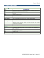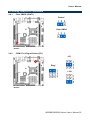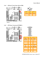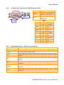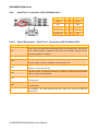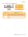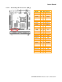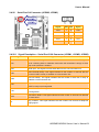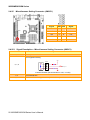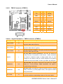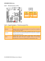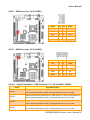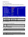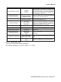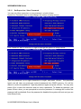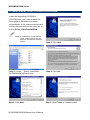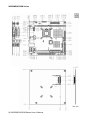
1
Mini-ITX
i855GME/i852GM
Series
Intel® Pentium® M / Celeron® M Mini ITX Main Board
User’s Manual
1st Ed – 23 June 2006
i855GME/i852GM Series
FCC Statement
THIS DEVICE COMPLIES WITH PART 15 FCC RULES. OPERATION IS
SUBJECT TO THE FOLLOWING TWO CONDITIONS:
(1) THIS DEVICE MAY NOT CAUSE HARMFUL INTERFERENCE.
(2) THIS DEVICE MUST ACCEPT ANY INTERFERENCE RECEIVED INCLUDING
INTERFERENCE THAT MAY CAUSE UNDESIRED OPERATION.
THIS EQUIPMENT HAS BEEN TESTED AND FOUND TO COMPLY WITH THE LIMITS
FOR A CLASS "A" DIGITAL DEVICE, PURSUANT TO PART 15 OF THE FCC RULES.
THESE LIMITS ARE DESIGNED TO PROVIDE REASONABLE PROTECTION AGAINST
HARMFUL INTERFERENCE WHEN THE EQUIPMENT IS OPERATED IN A
COMMERCIAL ENVIRONMENT. THIS EQUIPMENT GENERATES, USES, AND CAN
RADIATE RADIO FREQUENCY ENERGY AND, IF NOT INSTATLLED AND USED IN
ACCORDANCE WITH THE INSTRUCTION MANUAL, MAY CAUSE HARMFUL
INTERFERENCE TO RADIO COMMUNICATIONS.
OPERATION OF THIS EQUIPMENT IN A RESIDENTIAL AREA IS LIKELY TO CAUSE
HARMFUL INTERFERENCE IN WHICH CASE THE USER WILL BE REQUIRED TO
CORRECT THE INTERFERENCE AT HIS OWN EXPENSE.
Notice
This guide is designed for experienced users to setup the system within the shortest time.
For detailed information, please always refer to the electronic user's manual.
Copyright Notice
Copyright © 2006 Advansus Corp., ALL RIGHTS RESERVED.
No part of this document may be reproduced, copied, translated, or transmitted in any form
or by any means, electronic or mechanical, for any purpose, without the prior written
permission of the original manufacturer.
Trademark Acknowledgement
Brand and product names are trademarks or registered trademarks of their respective
owners.
2 i855GME/i852GM Series User’s Manual
User’s Manual
Disclaimer
Advansus Corp. reserves the right to make changes, without notice, to any product,
including circuits and/or software described or contained in this manual in order to improve
design and/or performance. Advansus Corp. assumes no responsibility or liability for the
use of the described product(s), conveys no license or title under any patent, copyright, or
masks work rights to these products, and makes no representations or warranties that
these products are free from patent, copyright, or mask work right infringement, unless
otherwise specified. Applications that are described in this manual are for illustration
purposes only. Advansus Corp. makes no representation or warranty that such application
will be suitable for the specified use without further testing or modification.
Life Support Policy
ADVANSUS CORP. PRODUCTS ARE NOT FOR USE AS CRITICAL COMPONENTS IN
LIFE SUPPORT DEVICES OR SYSTEMS WITHOUT THE PRIOR WRITTEN APPROVAL
OF ADVANSUS CORP.
As used herein:
1. Life support devices or systems are devices or systems which, (a) are intended for
surgical implant into body, or (b) support or sustain life and whose failure to perform,
when properly used in accordance with instructions for use provided in the labeling, can
be reasonably expected to result in significant injury to the user.
2. A critical component is any component of a life support device or system whose failure
to perform can be reasonably expected to cause the failure of the life support device or
system, or to affect its safety or effectiveness.
A Message to the Customer
Advansus Customer Services
Each and every Advansus product is built to the most exacting specifications to ensure
reliable performance in the harsh and demanding conditions typical of industrial
environments. Whether your new Advansus device is destined for the laboratory or the
factory floor, you can be assured that your product will provide the reliability and ease of
operation for which the name Advansus has come to be known.
Your satisfaction is our primary concern. Here is a guide to Advansus customer services.
To ensure you get the full benefit of our services, please follow the instructions below
carefully.
i855GME/i852GM Series User’s Manual 3
i855GME/i852GM Series
Technical Support
We want you to get the maximum performance from your products. So if you run into
technical difficulties, we are here to help. For the most frequently asked questions, you can
easily find answers in your product documentation. These answers are normally a lot more
detailed than the ones we can give over the phone. So please consult the user’s manual
first.
To receive the latest version of the user’s manual; please visit our Web site at:
http://www.Advansus.com.tw/
If you still cannot find the answer, gather all the information or questions that apply to your
problem, and with the product close at hand, call your dealer. Our dealers are well trained
and ready to give you the support you need to get the most from your Advansus products.
In fact, most problems reported are minor and are able to be easily solved over the phone.
In addition, free technical support is available from Advansus engineers every business day.
We are always ready to give advice on application requirements or specific information on
the installation and operation of any of our products. Please do not hesitate to call or e-mail
us.
Headquarters
Advansus Corp.
No.1, Alley 20, Lane 26, Rueiguang Road,
Neihu District, Taipei 114,
Taiwan
Tel : +886-2-2792-7818
Fax : +886-2-2794-7306
http://www.Advansus.com.tw
E-mail: [email protected]
4 i855GME/i852GM Series User’s Manual
User’s Manual
Product Warranty
Advansus warrants to you, the original purchaser, that each of its products will be free from
defects in materials and workmanship for two years from the date of purchase.
This warranty does not apply to any products which have been repaired or altered by
persons other than repair personnel authorized by Advansus, or which have been subject
to misuse, abuse, accident or improper installation. Advansus assumes no liability under
the terms of this warranty as a consequence of such events. Because of Advansus high
quality-control standards and rigorous testing, most of our customers never need to use our
repair service. If any of Advansus products is defective, it will be repaired or replaced at no
charge during the warranty period. For out-of-warranty repairs, you will be billed according
to the cost of replacement materials, service time, and freight. Please consult your dealer
for more details. If you think you have a defective product, follow these steps:
1. Collect all the information about the problem encountered. (For example, CPU type and
speed, Advansus products model name, hardware & BIOS revision number, other
hardware and software used, etc.) Note anything abnormal and list any on-screen
messages you get when the problem occurs.
2. Call your dealer and describe the problem. Please have your manual, product, and any
helpful information available.
3. If your product is diagnosed as defective, obtain an RMA (return material authorization)
number from your dealer. This allows us to process your good return more quickly.
4. Carefully pack the defective product, a complete Repair and Replacement Order Card
and a photocopy proof of purchase date (such as your sales receipt) in a shippable
container. A product returned without proof of the purchase date is not eligible for
warranty service.
5. Write the RMA number visibly on the outside of the package and ship it prepaid to your
dealer.
i855GME/i852GM Series User’s Manual 5
i855GME/i852GM Series
Contents
1. Getting Started..........................................................................................................10
1.1
Safety Precautions ..................................................................................................10
1.2
Packing List.............................................................................................................10
1.3
Document Amendment History ...............................................................................11
1.4
Manual Objectives...................................................................................................12
1.5
System Specifications .............................................................................................13
1.6
Architecture Overview .............................................................................................16
1.6.1
Block Diagram ................................................................................................................................ 16
1.6.2
Intel RG82855GME and FW82801DB ........................................................................................... 17
1.6.3
Intel RG82852GM and FW82801DB.............................................................................................. 19
1.6.4
DRAM Interface (Intel RG855GME)............................................................................................... 20
1.6.5
DRAM Interface (Intel RG852GM) ................................................................................................. 20
1.6.6
PCI Interface .................................................................................................................................. 20
1.6.7
IDE Interface (Bus Master Capability and Synchronous DMA Mode ) .......................................... 21
1.6.8
USB 2.0 .......................................................................................................................................... 21
1.6.9
VIA VT1616 Audio Codec .............................................................................................................. 21
1.6.10
Chrontel CH7009A TV/DVI Transmitter..................................................................................... 22
1.6.11
Ethernet...................................................................................................................................... 23
1.6.12
Winbond W83627HF.................................................................................................................. 25
1.6.13
Compact Flash Interface............................................................................................................ 25
2. Hardware Configuration...........................................................................................26
2.1
Product Overview....................................................................................................27
2.2
Installation Procedure .............................................................................................28
2.2.1
Processor Installation ..................................................................................................................... 28
2.2.2
Main Memory.................................................................................................................................. 30
2.3
2.4
Jumper and Connector List .....................................................................................32
Setting Jumpers & Connectors ...............................................................................35
2.4.1
Clear CMOS (JBAT1)..................................................................................................................... 35
2.4.2
COM1 Pin 9 Signal Select (JP1) .................................................................................................... 35
2.4.3
COM1 RS-232/422/485 Select (JP2, JP3)..................................................................................... 36
2.4.4
4/5/8-wire Touch Screen Select (SW1).......................................................................................... 37
2.4.5
ATX Power Connector (ATXPWR1)............................................................................................... 37
2.4.6
CPU Fan Connector (C_FAN1)...................................................................................................... 38
2.4.7
Parallel Port Connector & VGA Connector (CN1).......................................................................... 39
2.4.8
Serial Port 1 Connector in RS-232 Mode (CN1) ............................................................................ 40
2.4.9
Serial Port 1 Connector in RS-422 Mode (CN1) ............................................................................ 41
6 i855GME/i852GM Series User’s Manual
User’s Manual
2.4.10
Serial Port 1 Connector in RS-485 Mode (CN1)........................................................................ 42
2.4.11
Audio Connector (CN2).............................................................................................................. 43
2.4.12
RJ-45 Ethernet / USB 0 & 1, 4 & 5 Connectors (CN3, CN4) ..................................................... 43
2.4.13
4/5/8-Wire Touch Screen Connector (CN5)............................................................................... 43
2.4.14
Floppy Connector (FLP1)........................................................................................................... 44
2.4.15
Primary IDE Connector (IDE_1)................................................................................................. 46
2.4.16
Secondary IDE Connector (IDE_2)............................................................................................ 47
2.4.17
LCD Inverter Connector (JBKL1)............................................................................................... 49
2.4.18
CD-ROM Audio Input Connector (JCD1)................................................................................... 50
2.4.19
Serial Port 2 Connector (JCOM1).............................................................................................. 50
2.4.20
Serial Port 3/4 Connector (JCOM2, JCOM3)............................................................................. 51
2.4.21
Digital Input / Output Connector (JDIO1)................................................................................... 52
2.4.22
Front Panel Connector (JFP1) ................................................................................................... 53
2.4.23
IrDA Connector (JIR1) ............................................................................................................... 54
2.4.24
LVDS Connector (JLVDS1) ....................................................................................................... 55
2.4.25
Miscellaneous Setting Connector (JMISC1) .............................................................................. 56
2.4.26
TMDS Connector (JTMDS1)...................................................................................................... 57
2.4.27
TV Out Connector (JTV1) .......................................................................................................... 58
2.4.28
USB Connector 2 & 3 (JUSB1) .................................................................................................. 59
2.4.29
USB Connector 4 & 5 (JUSB2) .................................................................................................. 59
2.4.30
PS/2 Keyboard & Mouse Connector (KB_MS1) ........................................................................ 60
2.4.31
System Fan Connector 1 & 2 (S_FAN1, S_FAN2) .................................................................... 60
3 BIOS Setup................................................................................................................61
3.1
Starting Setup .........................................................................................................62
3.2
3.3
3.4
3.5
Using Setup ............................................................................................................63
Getting Help ............................................................................................................64
In Case of Problems................................................................................................64
Main Menu ..............................................................................................................65
3.5.1
Standard CMOS Features.............................................................................................................. 66
3.5.2
Advanced BIOS Features .............................................................................................................. 68
3.5.3
Advanced Chipset Features........................................................................................................... 71
3.5.4
Integrated Peripherals .................................................................................................................... 74
3.5.5
Power Management Setup............................................................................................................. 78
3.5.6
PnP / PCI Configuration ................................................................................................................. 80
3.5.7
PC Health Status............................................................................................................................ 81
3.5.8
Frequency / Voltage Control .......................................................................................................... 82
3.5.9
Load Fail-Safe Defaults.................................................................................................................. 83
3.5.10
Load Optimized Defaults............................................................................................................ 83
3.5.11
Set Supervisor / User Password................................................................................................ 84
3.5.12
Save & Exit Setup ...................................................................................................................... 85
i855GME/i852GM Series User’s Manual 7
i855GME/i852GM Series
3.5.13
Exit Without Save....................................................................................................................... 86
4 Drivers Installation ...................................................................................................87
4.1
Install Chipset Driver (For Intel RG82855GME) ......................................................88
4.2
Install Chipset Driver (For Intel 82852GM)..............................................................89
4.3
Install Display Driver (For Intel RG82855GME) ......................................................90
4.4
Install Display Driver (For Intel 82852GM) ..............................................................91
4.5
Install Audio Driver (For VIA VT1616) .....................................................................92
4.6
Install Ethernet Driver (For Realtek RTL810x, RTL813x Family) ............................93
4.7
Install Ethernet Driver (For Realtek RTL8110S)......................................................94
5 Measurement Drawing .............................................................................................95
Appendix A: BIOS Revisions ..........................................................................................97
Appendix B: AWARD BIOS POST Messages ................................................................98
Overview............................................................................................................................99
Post Beep ..........................................................................................................................99
Error Messages .................................................................................................................99
1.
CMOS BATTERY HAS FAILED ......................................................................................................... 99
2.
CMOS CHECKSUM ERROR ............................................................................................................. 99
3.
DISK BOOT FAILURE, INSERT SYSTEM DISK AND PRESS ENTER ............................................ 99
4.
DISKETTE DRIVES OR TYPES MISMATCH ERROR - RUN SETUP.............................................. 99
5.
DISPLAY SWITCH IS SET INCORRECTLY.................................................................................... 100
6.
DISPLAY TYPE HAS CHANGED SINCE LAST BOOT ................................................................... 100
7.
EISA Configuration Checksum Error PLEASE RUN EISA CONFIGURATION UTILITY................. 100
8.
EISA Configuration Is Not Complete PLEASE RUN EISA CONFIGURATION UTILITY ................. 100
9.
ERROR ENCOUNTERED INITIALIZING HARD DRIVE.................................................................. 100
10.
ERROR INITIALIZING HARD DISK CONTROLLER ................................................................... 100
11.
FLOPPY DISK CNTRLR ERROR OR NO CNTRLR PRESENT ................................................. 100
12.
Invalid EISA Configuration PLEASE RUN EISA CONFIGURATION UTILITY ............................ 101
13.
KEYBOARD ERROR OR NO KEYBOARD PRESENT ............................................................... 101
14.
Memory Address Error at ... ......................................................................................................... 101
15.
Memory parity Error at ................................................................................................................. 101
16.
MEMORY SIZE HAS CHANGED SINCE LAST BOOT ............................................................... 101
17.
Memory Verify Error at ... ............................................................................................................. 101
18.
OFFENDING ADDRESS NOT FOUND ....................................................................................... 101
19.
OFFENDING SEGMENT: ............................................................................................................ 101
20.
PRESS A KEY TO REBOOT ....................................................................................................... 102
21.
PRESS F1 TO DISABLE NMI, F2 TO REBOOT ......................................................................... 102
22.
RAM PARITY ERROR - CHECKING FOR SEGMENT ... ........................................................... 102
23.
Should Be Empty But EISA Board Found PLEASE RUN EISA CONFIGURATION UTILITY..... 102
24.
Should Have EISA Board But Not Found PLEASE RUN EISA CONFIGURATION UTILITY ..... 102
25.
Slot Not Empty ............................................................................................................................. 102
8 i855GME/i852GM Series User’s Manual
User’s Manual
26.
SYSTEM HALTED, (CTRL-ALT-DEL) TO REBOOT ... ............................................................... 102
27.
Wrong Board In Slot PLEASE RUN EISA CONFIGURATION UTILITY...................................... 103
28.
FLOPPY DISK(S) fail (80) → Unable to reset floppy subsystem................................................. 103
29.
FLOPPY DISK(S) fail (40) → Floppy Type dismatch................................................................... 103
30.
Hard Disk(s) fail (80) → HDD reset failed.................................................................................. 103
31.
Hard Disk(s) fail (40) → HDD controller diagnostics failed........................................................ 103
32.
Hard Disk(s) fail (20) → HDD initialization error........................................................................ 103
33.
Hard Disk(s) fail (10) → Unable to recalibrate fixed disk........................................................... 103
34.
Hard Disk(s) fail (08) → Sector Verify failed.............................................................................. 103
35.
Keyboard is locked out - Unlock the key. ..................................................................................... 103
36.
Keyboard error or no keyboard present. ...................................................................................... 103
37.
Manufacturing POST loop............................................................................................................ 103
38.
BIOS ROM checksum error - System halted. .............................................................................. 103
39.
Memory test fail. ........................................................................................................................... 103
40.
POST Codes ................................................................................................................................ 104
i855GME/i852GM Series User’s Manual 9
i855GME/i852GM Series
1. Getting Started
1.1 Safety Precautions
Warning!
Always completely disconnect the power cord from your
chassis whenever you work with the hardware. Do not
make connections while the power is on. Sensitive
electronic components can be damaged by sudden power
surges. Only experienced electronics personnel should
open the PC chassis.
Caution!
Always ground yourself to remove any static charge before
touching the CPU card. Modern electronic devices are very
sensitive to static electric charges. As a safety precaution,
use a grounding wrist strap at all times. Place all electronic
components in a static-dissipative surface or static-shielded
bag when they are not in the chassis.
1.2 Packing List
Before you begin installing your single board, please make sure that the
following materials have been shipped:
z
1 x i855GME Intel Socket 478/479 Pentium® M/Celeron® M Mini ITX
Main Board (Onboard Intel® Celeron® M 600 MHz with 0K L2 Cache or
Intel® Processor at 800 MHz
z
1 x CD-ROM or DVD-ROM contains the followings:
z
— User’s Manual (this manual in PDF file)
— Ethernet driver and utilities
— VGA drivers and utilities
— Audio drivers and utilities
1 x Cable set contains the followings:
z
— 1 x IDE HDD cable (40-pin, pitch 2.54mm)
— 1 x IDE HDD cable (44-pin, pitch 2.0mm)
— 1 x FDD cable (34-pin, pitch 2.54mm)
— 1 x Serial port cable with 3 DB9P(M) (10-pin, pitch 2.54mm)
— 1 x I/O shield
1 x Pentium® M CPU cooler
10 i855GME/i852GM Series User’s Manual
User’s Manual
1.3 Document Amendment History
Revision
st
1
Date
By
Jun., 2006
Juliet Chen
Comment
Initial Release
i855GME/i852GM Series User’s Manual 11
i855GME/i852GM Series
1.4 Manual Objectives
This manual describes in detail the Advansus Technology i855GME series Single Board.
We have tried to include as much information as possible but we have not duplicated
information that is provided in the standard IBM Technical References, unless it proved to
be necessary to aid in the understanding of this board.
We strongly recommend that you study this manual carefully before attempting to interface
with i855GME series or change the standard configurations. Whilst all the necessary
information is available in this manual we would recommend that unless you are confident,
you contact your supplier for guidance.
Please be aware that it is possible to create configurations within the CMOS RAM that
make booting impossible. If this should happen, clear the CMOS settings, (see the
description of the Jumper Settings for details).
If you have any suggestions or find any errors concerning this manual and want to inform
us of these, please contact our Customer Service department with the relevant details.
12 i855GME/i852GM Series User’s Manual
User’s Manual
1.5 System Specifications
System
i855GME-DCQI
Model
Supports Intel® µFC-PGA 478 / µFC-BGA 479 Pentium® M / Celeron® M up to 1.8
CPU
GHz with 0.13µ and 90nm process technology
FSB
400 MHz
BIOS
Award 512 KB Flash BIOS
System Chipset
Intel® RG82855GME GMCH/FW82801DB ICH4
I/O Chip
Winbond W83627HF-AW
System Memory
One 184-pin DIMM socket supports up to 1 GB DDR 266/333 SDRAM
SSD
One CompactFlash Type I/II socket
Watchdog Timer
Reset: 1 sec.~255 min. and 1 sec. or 1 min./step
Monitoring system temperature, voltage, and cooling fan status. Auto throttling
H/W Status Monitor
Expansion
control when CPU overheats.
One PCI slot (PCI Rev. 2.2 compliant), one Mini PCI slot
I/O
4 x EIDE (Ultra DMA 100), 2 x FDD , 1 x LPT, 1 x RS-232, 1x RS-232/422/485, 1x
MIO
K/B,
1 x Mouse
IrDA
115k bps, IrDA 1.0 compliant
USB
6 USB 2.0 ports
DIO
16-bit General Purpose I/O for DI and DO
i855GME/i852GM Series User’s Manual 13
i855GME/i852GM Series
Display
i855GME-DCQI
Model
Chipset
Intel® RG82855GME GMCH integrated Extreme Graphics 2 controller
Display Memory
Intel® DVMT 2.1 supports up to 64 MB video memory
CRT mode: 1600 x 1200 @ 32 bpp (85 Hz)
Resolution
LCD/Simultaneous mode: 1600 x 1200 @ 32 bpp (85 Hz)
Dual Display
CRT + LVDS, or DVI/TV-out + LVDS or CRT + DVI
LVDS
Dual-channel 18/24-bit LVDS
DVI
Chrontel CH7009A DVI transmitter up to 135M pixels/second
Chrontel CH7009A TV encoder supports both NTSC/PAL
TV-Out
Supports both S-Video and composite video
Built-in Touch Screen
(Optional)
Chipset
PenMount DMC9000
Touch Screen Interface
With 9-pin 2 mm box header (can be selected with 4/5/8-wire connector)
Audio
Chipset
Intel® 82801DB ICH4
AC97 Codec
VIA VT1616 supports 5.1 CH Audio
Audio Interface
Mic in, Line in, CD Audio in, Line out
Ethernet
LAN1
Realtek RTL8110S Gigabit LAN
LAN2
N/A
Ethernet Interface
1000Base-T Fast Ethernet compatible: Realtek RTL8110S
14 i855GME/i852GM Series User’s Manual
User’s Manual
Mechanical & Environmental
i855GME-DCQI
Model
+5 V @ 3.34 A, +12 V @ 0.09 A, +3.3 V @ 3.74 A, 5 Vsb @ 0.23 A (with Intel®
Power Requirement
Pentium® M 1.8 GHz & 256 MB DDR SDRAM)
Power Type
AT/ATX
Operation Temperature
0~60o C (32~140 o F)
Operating Humidity
0%~90% relative humidity, non-condensing
Size ( L x W )
6.69" x 6.69" (170 mm x 170 mm)
Weight
0.88 lbs (0.4 Kg)
i855GME/i852GM Series User’s Manual 15
i855GME/i852GM Series
1.6 Architecture Overview
1.6.1
Block Diagram
The following block diagram shows the architecture and main components of
i855GME-DCQI.
The following sections provide detail information about the functions provided onboard.
16 i855GME/i852GM Series User’s Manual
User’s Manual
1.6.2
Intel RG82855GME and FW82801DB
The Intel 855GM/855GME GMCH components provide the processor interface, DDR
SDRAM interface, display interface, and Hub interface. The Intel 855GME also has an
option for AGP external graphics port, in addition to integrated graphics support for added
board flexibility options.
The Intel 855GM GMCH is in a 732-pin Micro-FCBGA package and contains the following
functionality listed below:
AGTL+ host bus supporting 32-bit host addressing with Enhanced Intel SpeedStep
technology support
• Supports a single channel of DDR SDRAM memory
• System memory supports DDR200/266 MHz (SSTL_2) DDR SDRAM
• Integrated graphics capabilities: Display Core frequency at 133 MHz or 200 MHz
• Render Core frequency at 100 MHz ,133 MHz, and 200 MHz
• Provides supports four display ports: one progressive scan analog monitor, dual
channel LVDS interface and two DVO port.
The Intel 855GME GMCH is in a 732-pin Micro-FCBGA package and contains all features
listed above and the additional functionality list below:
• Display Core frequency at 133 MHz, 200 MHz, or 250 MHz
• Render Core frequency at 100 MHz ,133 MHz, 166 MHz, 200 MHz, or 250 MHz
• System memory supports 200/266/333- MHz (SSTL_2) DDR SDRAM.
• Enhanced Power Management Graphics features
The GMCH IGD provides a highly integrated graphics accelerator delivering high
performance 2D, 3D, and video capabilities. With its interfaces to UMA using a DVMT
configuration, an analog display, a LVDS port, and two digital display ports (e.g. flat panel),
the GMCH can provide a complete graphics solution.
The GMCH also provides 2D hardware acceleration for block transfers of data (BLTs). The
BLT engine provides the ability to copy a source block of data to a destination and perform
raster operations (e.g., ROP1, ROP2, and ROP3) on the data using a pattern, and/or
another destination. Performing these common tasks in hardware reduces CPU load, and
thus improves performance. High bandwidth access to data is provided through the system
memory interface. The GMCH uses Tiling architecture to increase system memory
efficiency and thus maximize effective rendering bandwidth. The Intel 855GM/855GME
GMCH improves 3D performance and quality with 3D Zone rendering technology. The Intel
855GME GMCH also supports Video Mixer rendering and Bi-Cubic filtering.
•
i855GME/i852GM Series User’s Manual 17
i855GME/i852GM Series
The Intel 855GM/855GME GMCH has four display ports, one analog and three digital. With
these interfaces, the GMCH can provide support for a progressive scan analog monitor, a
dedicated dual channel LVDS LCD panel, and two DVO devices. Each port can transmit
data according to one or more protocols. The data that is sent out the display port is
selected from one of the two possible sources, Pipe A or Pipe B.
The Intel 855GM/855GME GMCH have an integrated dual channel LFP Transmitter
interface to support LVDS LCD panel resolutions up to UXGA The display pipe provides
panel up-scaling to fit a smaller source image onto a specific native panel size, as well as
provides panning and centering support. The LVDS port is only supported on Pipe B. The
LVDS port can only be driven by Pipe B, either independently or simultaneously with the
Analog Display port. Spread Spectrum Clocking is supported: center and down spread
support of 0.5%, 1%, and 2.5% utilizing an external SSC clock.
The DVO B/C interface is compliant with the DVI Specification 1.0. When combined with a
DVI compliant external device (e.g. TMDS Flat Panel Transmitter, TV-out encoder, etc.),
the GMCH provides a high-speed interface to a digital or analog display (e.g. flat panel, TV
monitor, etc.). The DVO ports are connected to an external display device. Examples of this
are TV-out encoders, external DACs, LVDS transmitters, and TMDS transmitters. Each
display port has control signals that may be used to control, configure and/or determine the
capabilities of an external device. The GMCH provides two DVO ports that are each
capable of driving a 165-MHz pixel clock at the DVO B or DVO C interface. When DVO B
and DVO C are combined into a single DVO port, then an effective pixel rate of 330 MHz
can be achieved. The DVO B/C ports can be driven by Pipe A or Pipe
B. If driven on Pipe B, then the LVDS port must be disabled.
The ICH4 is a highly integrated multifunctional I/O Controller Hub that provides the
interface to the PCI Bus and integrates many of functions needed in today’s PC platform.
The GMCH and ICH4 communicate over a dedicated hub interface. The 82801DB ICH4
functions and capabilities include:
• PCI Rev. 2.2 compliant with support for 33MHz PCI operations
• Supports up to 6 Request/Grant pairs (PCI slots)
• Power management logic support
• Enhanced DMA controller, interrupt controller, and timer functions
• Integrated IDE controller; Ultra ATA/100/66/33
• USB host interface; 3 host controllers and supports 6 USB ports; includes a EHCI
high-speed 2.0 USB controller
18 i855GME/i852GM Series User’s Manual
User’s Manual
•
•
•
•
•
•
Integrated LAN controller
System Management Bus (SMBus) compatible with most IC devices; ICH4 has both
bus master and slave capability
AC ’97 2.3 compliant link for audio and telephony codecs; up to 6 channels
Low Pin Count (LPC) interface
FWH Interface (FWH Flash BIOS support)
Alert on LAN* (AOL and AOL2)
1.6.3
Intel RG82852GM and FW82801DB
The Intel 852GM GMCH component provides the processor interface, DDR SDRAM
interface, display interface, and Hub Interface in an Intel 852GM chipset platform. The Intel
852GM GMCH is optimized for the Mobile Intel Pentium 4 Processor-M, Mobile Intel
Celeron processor and Intel Celeron M processor. It supports a single channel of DDR
SDRAM memory. Intel 852GM Chipset contains advanced power management logic. The
Intel 852GM Chipset platform supports the fourth generation mobile I/O Controller Hub to
provide the features required by a mobile platform.
The Intel 852GM GMCH is in a 732-pin Micro-FCBGA package and contains the following
functionality:
• Supports single Intel processor configurations at 400-MHz or 3 GB/s
• 1.2-1.30-V AGTL+ host bus supporting 32-bit host bus addressing with Enhanced
Intel SpeedStep® technology (Intel Celeron M processor and Intel Celeron
Processor do not support Enhanced Intel SpeedStep Technology).
• System Memory supports 200/266-MHz (SSTL_2) DDR DRAM Up to 1 GB (with
256-Mb technology and two SO-DIMMs) of PC1600/2100 DDR SDRAM without
ECC
• Integrated graphics capabilities, including 3D rendering acceleration and 2D
hardware acceleration
• Integrated 350-MHz, 24-bit RAMDAC with pixel resolution up to 1600x1200 at 85-Hz
and up to 1920x1440 @ 60 Hz
• One Dedicated Dual Channel LFP LVDS interface with frequency range of 25 MHz
to 112 MHz (single channel/dual channel) for support up to SXGA+ (1400x1050 @
60 Hz) panel resolutions with maximum pixel depth of 18-bpp
• Integrated PWM (Pulse Width Modulation) interface for LFP backlight inverter
control for panel brightness
• One 165-MHz, 12-bit, DVO interface for TV-out encoder and DVI (LVDS transmitter
and TMDS transmitter) support I2C and DDC channels supported
• Dual Pipe Independent Display with Tri-view support through LFP, DVO, and CRT
• Deeper Sleep state support
i855GME/i852GM Series User’s Manual 19
i855GME/i852GM Series
•
•
•
•
•
•
•
Distributed arbitration for highly concurrent operation
Three USB host controllers provide high performance peripherals with 480 Mbps of
bandwidth, while enabling support for up to six USB 2.0 ports. This results in a
significant increase over previous integrated 1-4 port hubs at 12 Mbps
The latest AC ’97 implementation delivers 20-bit audio for enhanced sound quality
and full surround sound capability. Integrated audio solutions continue to enjoy
success as a very cost-effective, yet high-performance solution
LAN Connect Interface (LCI) provides flexible network solutions such as 10/100
Mbps Ethernet and 10/100 Mbps Ethernet with LAN manageability
Dual Ultra ATA/100 controllers, coupled with the Intel® Application Accelerator – a
performance software package – support faster IDE transfers to storage devices
Intel Application Accelerator software provides additional performance over native
ATA drivers by improving I/O transfer rates and enabling faster O/S load time,
resulting in accelerated boot times
Communication and Network Riser (CNR) offers flexibility in system configuration
with a baseline feature set that can be upgraded with an audio card, modem card, or
network card
1.6.4
DRAM Interface (Intel RG855GME)
The 855GME GMCH system memory controller directly supports the following:
• One channel of PC1600/2100/2700 DDR SDRAM memory
• DDR SDRAM devices with densities of 128-Mb, 256-Mb, and 512-Mb technology
• Up to 1 GB (512-Mb technology) SDRAM
1.6.5
DRAM Interface (Intel RG852GM)
The 852GM GMCH system memory controller directly supports the following:
• One channel of PC1600/2100 DDR SDRAM memory
• DDR SDRAM devices with densities of 128-Mb, 256-Mb, and 512-Mb technology
• Variable page sizes of 2-kB, 4-kB, 8-kB, and 16-kB. Page size is individually selected
for every row and a maximum of 16 pages may be opened simultaneously
1.6.6
PCI Interface
The ICH4 PCI interface provides a 33 MHz, Rev. 2.2 compliant implementation. All PCI
signals are 5V tolerant, except PME#. The ICH2 integrates a PCI arbiter that supports up to
six external PCI bus masters in addition to the internal ICH4 requests.
20 i855GME/i852GM Series User’s Manual
User’s Manual
1.6.7
IDE Interface (Bus Master Capability and Synchronous DMA Mode )
The fast IDE interface supports up to four IDE devices providing an interface for IDE hard
disks and ATAPI devices. Each IDE device can have independent timings. The IDE
interface supports PIO IDE transfers up to 16 Mbytes/sec and Ultra ATA transfers up 100
Mbytes/sec. It does not consume any ISA DMA resources. The IDE interface integrates
16x32-bit buffers for optimal transfers.
The ICH4’s IDE system contains two independent IDE signal channels. They can be
electrically isolated independently. They can be configured to the standard primary and
secondary channels (four devices). There are integrated series resistors on the data and
control lines.
Access to these controllers is provided by two standard IDC 40-pin connectors.
1.6.8
USB 2.0
The ICH4 contains an Enhanced Host Controller Interface (EHCI) compliant host controller
that supports USB high-speed signaling. High-speed USB 2.0 allows data transfers up to
480Mb/s which is 40 times faster than full-speed USB. The ICH4 also contains three
Universal Host Controller Interface (UHCI) controllers that support USB full-speed and
low-speed signaling.
The ICH4 supports 6 USB 2.0 ports. All six USB ports are high-speed, full-speed, and
low-speed capable. ICH4’s port-routing logic determines whether a USB port is controlled
by one of the UHCI controllers or by the EHCI controller.
1.6.9
VIA VT1616 Audio Codec
VIA Technologies’ VT1616TM 18-bit audio codec conforms to the AC’97 2.2 specifications.
The VT1616 integrates Sample Rate Converters on all channels and can be adjusted in
1Hz increments. There is a provision in hardware for down-mixing the 6 channels into
stereo when only two end points are available. The analog mixer circuitry integrates a
stereo enhancement to provide a pleasing 3D surround sound effect for stereo media. This
codec is designed with aggressive power management to achieve low power consumption.
When used with a 3.3V analog supply, power consumption is further reduced. The primary
applications for this part are desktop and portable personal computers multimedia
subsystems.
i855GME/i852GM Series User’s Manual 21
i855GME/i852GM Series
1.6.10 Chrontel CH7009A TV/DVI Transmitter
The Chrontel CH7009A is a display controller device which accepts a digital graphics input
signal, and encodes and transmits data through a DVI (DFP can also be supported) or TV
output (analog composite, s-video or RGB). The device accepts data over one 12-bit wide
variable voltage data port which supports five different data formats including RGB and
YCrCb.
The DVI processor includes a low jitter PLL for generation of the high frequency serialized
clock, and all circuitries are required to encode, serialize and transmit data. The CH7009
comes in versions able to drive a DVI display at a pixel rate of up to 165MHz, supporting
UXGA resolution displays. No scaling of input data is performed on the data output to the
DVI device.
The TV-Out processor performs non-interlace to interlace conversion with scaling and
flicker filters, and encode the data into any of the NTSC or PAL video standards. The
scaling and flicker filter is adaptive and programmable to enable superior text display.
Eight graphics resolutions are supported up to 1024 by 768 with full vertical and horizontal
underscan capability in all modes. A high accuracy low jitter phase locked loop is
integrated to create outstanding video quality. Support is provided for MacrovisionTM and
RGB bypass mode which enables driving a VGA CRT with the input data.
22 i855GME/i852GM Series User’s Manual
User’s Manual
1.6.11 Ethernet
1.6.11.1 Realtek RTL8100C Ethernet Controller
The Realtek RTL8100C(L) is a highly integrated, cost-effective single-chip Fast Ethernet
controller that provides 32-bit performance, PCI bus master capability, and full compliance
with IEEE 802.3u 100Base-T and Power Interface (ACPI), PCI power management for
modern operating systems that are cpable of Operating System-Directed Power
Management (OSPM) to achieve that most efficient power management possible. The
RTL8100C(L) does not support CardBus mode (the RTL8139C does).
In addition to the ACPI feature, the RTL8100C(L) also supports remote wake-up (including
AMD magic Packet, LinkChg, and Microsoft® wake-up frame) in both ACPI and APM
(Advanced Power Management) environments. The RTL8100C(L) is capable of performing
an internal reset through the application of auxiliary power. When auxiliary power is applied
and the main power remains off, the RTL8100C(L) is ready and waiting for a Magic Packet
or Link Change to wake the system up. Also, the LWAKE pin provides 4 output signals
(active high, active low, positive pulse, and negative pulse). The versatility of the
RTL8100C(L) LWAKE pin provides motherboards, with Wake-On-LAN (WOL) functionality.
The RTL8100C(L) also supports Analog Auto-Power-down. The analog part of the
RTL8100C(L) can be shut down temporarily according to user requirements, or when the
RTL8100C(L) is in a power down state with the wakeup function disabled. When the analog
part is shut down and the IsolateB pin is low (i.e. the main power is off), both the analog and
digital parts stop functioning and the power consumption of the RTL8100C(L) is negligible.
The RTL8100C(L) also supports an auxiliary power auto-detect function, and will
auto-configure related bits of its PCI power management registers in PCI configuration
space.
PCI Vital Product Data (VPD) is also supported to provide hardware identifier information.
The information may consist of part number, serial number, OEM brand name, and other
detailed information.
i855GME/i852GM Series User’s Manual 23
i855GME/i852GM Series
1.6.11.2 Realtek RTL8100S Gigabit Ethernet Controller
The Realtek RTL8110SB(L) LOM Gigabit Ethernet controllers (RTL8110SB (128 QFP) &
RTL8110SBL (128 LQFP)) combine a triple-speed IEEE 802.3 compliant Media Access
Controller (MAC) with a triple-speed Ethernet transceiver, 32-bit PCI bus controller, and
embedded memory. With state-of-the-art DSP technology and mixed-mode signal
technology, they offer high-speed transmission over CAT 5 UTP cable or CAT 3 UTP
(10Mbps only) cable. Functions such as Crossover Detection & Auto-Correction, polarity
correction, adaptive equalization, cross-talk cancellation, echo cancellation, timing recovery,
and error correction are implemented to provide robust transmission and reception
capability at high speeds.
The devices support the PCI v2.3 bus interface for host communications with power
management and are compliant with the IEEE 802.3 specification for 10/100Mbps Ethernet
and the IEEE 802.3ab specification for 1000Mbps Ethernet. They also support an auxiliary
power auto-detect function, and will auto-configure related bits of the PCI power
management registers in PCI configuration space.
They support the Advanced Configuration Power management Interface (ACPI)--power
management for modern operating systems that are capable of Operating System-directed
Power Management (OSPM)--to achieve the most efficient power management possible.
PCI Message Signaled Interrupt (MSI) is also supported.
In addition to the ACPI feature, the RTL8110SB(L) support remote wake-up (including AMD
Magic Packet, Re-LinkOk, and Microsoft® Wake-up frame) in both ACPI and APM
(Advanced Power Management) environments. The LWAKE pin provides four different
output signals including active high, active low, positive pulse, and negative pulse. The
versatility of the LWAKE pin provides motherboards with Wake-On-LAN (WOL)
functionality. To support WOL from a deep power down state (e.g. D3cold, i.e. main power
is off and only auxiliary exists), the auxiliary power source must be able to provide the
needed power for the RTL8110SB(L).
The RTL8110SB(L) is fully compliant with Microsoft® NDIS5 (IP, TCP, UDP) Checksum
and Segmentation Task-offload features, and supports IEEE 802 IP Layer 2 priority
encoding and 802.1Q Virtual bridged Local Area Network (VLAN). The above features
contribute to lowering CPU utilization, especially benefiting performance when in operation
on a network server. Also, the devices boost their PCI performance by supporting PCI
Memory Read Line & Memory Read Multiple when transmitting, and Memory Write and
Invalidate when receiving. To better qualify for server use, the RTL8110SB(L) support the
PCI Dual Address Cycle (DAC) command when the assigned buffers reside at a physical
memory address higher than 4 Gigabytes.
24 i855GME/i852GM Series User’s Manual
User’s Manual
1.6.12 Winbond W83627HF
The Winbond W83627F/HF is made to fully comply with Microsoft PC98 and PC99
Hardware Design Guide. Moreover, W83627F/HF is made to meet the specification of
PC98/PC99’s requirement in the power management: ACPI and DPM (Device Power
Management). Super I/O chip provides features as the following:
• Meet LPC Spec. 1.0
• Support LDRQ# (LPC DMA), SERIRQ (serial IRQ)
• Include all features of Winbond I/O W83977TF and W83977EF
• Integrate Hardware Monitor functions
• Compliant with Microsoft PC98/PC99 Hardware Design Guide.
• Support DPM (Device Power Management), ACPI
• Programmable configuration settings
• Single 24 or 48 MHz clock input
1.6.13 Compact Flash Interface
A Compact Flash type II connector is connected to the secondary IDE controller. The
Compact Flash storage card is IDE compatible. It is an ideal replacement for standard IDE
hard drives. The solid-state design offers no seek errors even under extreme shock and
vibration conditions. The Compact Flash storage card is extremely small and highly suitable
for rugged environments, thus providing an excellent solution for mobile applications with
space limitations. It is fully compatible with all consumer applications designed for data
storage PC card, PDA, and Smart Cellular Phones, allowing simple use for the end user.
The Compact Flash storage card is O/S independent, thus offering an optimal solution for
embedded systems operating in non-standard computing environments. The Compact
Flash storage card is IDE compatible and offers various capacities.
i855GME/i852GM Series User’s Manual 25
i855GME/i852GM Series
2. Hardware
Configuration
26 i855GME/i852GM Series User’s Manual
User’s Manual
2.1 Product Overview
i855GME/i852GM Series User’s Manual 27
i855GME/i852GM Series
2.2 Installation Procedure
This chapter explains you the instructions of how to setup your system.
1. Turn off the power supply.
2. Insert the DIMM module (be careful with the orientation).
3. Insert all external cables for hard disk, floppy, keyboard, mouse, USB etc. except for flat
panel. A CRT monitor must be connected in order to change CMOS settings to support
flat panel.
4. Connect power supply to the board via the ATXPWR.
5. Turn on the power.
6. Enter the BIOS setup by pressing the delete key during boot up. Use the “LOAD BIOS
DEFAULTS” feature. The Integrated Peripheral Setup and the Standard CMOS Setup
Window must be entered and configured correctly to match the particular system
configuration.
7. If TFT panel display is to be utilized, make sure the panel voltage is correctly set before
connecting the display cable and turning on the power.
2.2.1
Processor Installation
2.2.1.1 Installing Pentium M CPU
• The processor socket comes with a screw to secure the processor, please unlock the
screw first.
• Position the CPU above the socket and the gold triangular mark on the CPU must
align with pin 1 of the CPU socket. Then Insert the CPU gently seated in place.
• Turn the screw to the lock position.
Unlock
Pin 1 of the
socket
Lock
Gold
triangular
mark
Note: Do not force the CPU into the socket. It may bend the pins and damage the
CPU.
28 i855GME/i852GM Series User’s Manual
User’s Manual
2.2.1.2
Installing the Fan and Heat Sink
• Insert the copper studs to the screw holes around the CPU socket from the top
through the rear side of the board with screw nuts fastened.
Copper Stud
Screw hole
Screw nut
(Rear side)
• Match and place the CPU fan and heat sink assembly on the top of the CPU and
copper studs. Tighten the screws into the copper studs through washers and the
screw holes around the heat sink.
• Place the CPU Fan Connector.
CPU Fan & heat
sink assembly
Washers
Screws
CPU fan
connector
Note: Make sure the CPU fan and heat sink assembly and the CPU top surface
are in total contact to avoid CPU overheating problem that would cause the
system to hang or unstable
2.2.1.3
•
•
•
•
•
•
Removing CPU
Disconnect the CPU fan connector.
Remove the CPU fan and heat sink assembly first.
Unfasten the copper studs from the board.
Unlock the Pentium M processor.
Carefully lift up the existing CPU to remove it from the socket.
Follow the steps of installing a CPU to change to another one.
i855GME/i852GM Series User’s Manual 29
i855GME/i852GM Series
2.2.2
Main Memory
i855GME provides one 184-pin DIMM socket to support DDR SDRAM. The total maximum
memory size is 1GB.
DIMM1
Make sure to unplug the power supply before adding or removing DIMMs or
other system components. Failure to do so may cause severe damage to
both the board and the components.
30 i855GME/i852GM Series User’s Manual
User’s Manual
•
•
•
•
Locate the DIMM slot on the board.
Hold two edges of the DIMM module carefully. Keep away of touching its connectors.
Align the notch key on the module with the rib on the slot.
Firmly press the modules into the slot automatically snaps into the mounting notch. Do
not force the DIMM module in with extra force as the DIMM module only fit in one
direction.
• To remove the DIMM modules, push the two ejector tabs on the slot outward
simultaneously, and then pull out the DIMM module.
Note: (1) Please do not change any DDR SDRAM parameter in BIOS setup to
increase your system’s performance without acquiring technical
information in advance.
(2) Static electricity can damage the electronic components of the computer
or optional boards. Before starting these procedures, ensure that you
are discharged of static electricity by touching a grounded metal object
briefly.
i855GME/i852GM Series User’s Manual 31
i855GME/i852GM Series
2.3 Jumper and Connector List
You can configure your board to match the needs of your application by setting jumpers. A
jumper is the simplest kind of electric switch.
It consists of two metal pins and a small metal clip (often protected by a plastic cover) that
slides over the pins to connect them. To “close” a jumper you connect the pins with the clip.
To “open” a jumper you remove the clip. Sometimes a jumper will have three pins, labeled 1,
2, and 3. In this case, you would connect either two pins.
The jumper settings are schematically depicted in this manual as follows:
A pair of needle-nose pliers may be helpful when working with jumpers.
Connectors on the board are linked to external devices such as hard disk drives, a
keyboard, or floppy drives. In addition, the board has a number of jumpers that allow you to
configure your system to suit your application.
If you have any doubts about the best hardware configuration for your application, contact
your local distributor or sales representative before you make any changes.
The following tables list the function of each of the board's jumpers and connectors.
Jumpers
Label
Function
Note
JBAT1
Clear CMOS
3 x 1 header, pitch 2.54mm
JP1
COM1 pin 9 signal select
3 x 2 header, pitch 2.0mm
JP2, JP3
COM1 RS-232/422/485 select
3 x 2 header, pitch 2.0mm
4 x 3 header, pitch 2.0mm
SW1
4/5/8-wire touch screen select
Switch
SW2
Reserved
Switch
32 i855GME/i852GM Series User’s Manual
User’s Manual
Connectors
Label
Function
Note
ATXPWR1
ATX Power connector
ATX power connector
C_FAN1
CPU fan connector
3 x 1 wafer, pitch 2.54mm
CF1
CF card connector
CN1
Parallel port connector
Serial port 1 connector
VGA connector
D-sub 25-pin, female
D-sub 9-pin, male
D-sub 15-pin, female
CN2
Audio connector
Phone Jack X 3
CN4
RJ-45 Ethernet / USB 0 & 1 connector
CN5
4/5/8-wire touch screen connector
DIMM1
184-pin DDR SDRAM DIMM socket
FLP1
Floppy connector
17 x 2 header, pitch 2.54mm
IDE_1
Primary IDE connector
20 x 2 header, pitch 2.54mm
IDE_2
Secondary IDE connector
22 x 2 header, pitch 2.0mm
JBKL1
LCD inverter connector
5 x 1 wafer, pitch 2.0mm
JCD1
CD-ROM audio input connector
4 x 1 wafer, pitch 2.0mm
JCOM1
Serial port 2 connector
5 x 2 header, pitch 2.54mm
JCOM2
Serial port 3 connector
5 x 2 header, pitch 2.54mm
JCOM3
Serial port 4 connector
5 x 2 header, pitch 2.54mm
JDIO1
Digital input/output connector
10 x 2 header, pitch 2.54mm
JFP1
Front panel connector
8 x 2 header, pitch 2.54mm
JIR1
IrDA connector
5 x 1 header, pitch 2.54mm
JLVDS1
LVDS connector
HIROSE DF13-40DP-1.25V
JMISC1
Miscellaneous setting connector
5 x 2 header, pitch 2.54mm
JTMDS1
TMDS connector
HIROSE DF13-20DP-1.25V
JTV1
TV out connector
3 x 2 header, pitch 2.54mm
JUSB1
USB connector 2 & 3
5 x 2 header, pitch 2.54mm
JUSB2
USB connector 4 & 5
5 x 2 header, pitch 2.54mm
9 x 1 wafer, pitch 2.0mm
i855GME/i852GM Series User’s Manual 33
i855GME/i852GM Series
Connectors
Label
Function
Note
KB_MS1
PS/2 Keyboard & mouse connector
6-pin Mini-DIN x 2
MPCI1
Mini PCI slot
PCI1
PCI slot
S_FAN1,S_FAN2 System fan connector 1 & 2
34 i855GME/i852GM Series User’s Manual
3 x 1 wafer, pitch 2.54mm
User’s Manual
2.4 Setting Jumpers & Connectors
2.4.1
Clear CMOS (JBAT1)
Protect*
Clear CMOS
* Default
2.4.2
COM1 Pin 9 Signal Select (JP1)
+5V
Ring*
+12V
* Default
i855GME/i852GM Series User’s Manual 35
i855GME/i852GM Series
2.4.3
COM1 RS-232/422/485 Select (JP2, JP3)
(JP2)
RS-232*
(JP3)
RS-232*
RS-422
RS-422
RS-485
RS-485
JP2
JP3
* Default
36 i855GME/i852GM Series User’s Manual
User’s Manual
2.4.4
4/5/8-wire Touch Screen Select (SW1)
Wire
BIT1
BIT2
* 4, 8
OFF
ON
5
ON
OFF
* Default
2.4.5
ATX Power Connector (ATXPWR1)
Signal
PIN
PIN
Signal
+12V
10
20
+5V
VCCSB
9
19
+5V
PWROK
8
18
-5V
GND
7
17
GND
+5V
6
16
GND
GND
5
15
GND
+5V
4
14
PS_ON
GND
3
13
GND
+3.3V
2
12
-12V
+3.3V
1
11
+3.3V
i855GME/i852GM Series User’s Manual 37
i855GME/i852GM Series
2.4.6
CPU Fan Connector (C_FAN1)
Signal
PIN
TAC
3
+12V
2
GND
1
2.4.6.1 Signal Description – CPU Fan Connector (C_FAN1)
Signal
TAC
Signal Description
Fan speed monitor
38 i855GME/i852GM Series User’s Manual
User’s Manual
2.4.7
Parallel Port Connector & VGA Connector (CN1)
Port
Parallel
VGA
Description
Connects a parallel printer, a
scanner, or other devices.
For pointing devices or other
COM
serial devices
VGA
COM
Signal
RED
PIN
Signal
6
GND
1
11
7
GREEN
2
GND
12
8
BLUE
3
13
4
5
HSYNC
VCC
14
10
GND
DAT
GND
9
NC
NC
VSYNC
GND
15
DCK
2.4.7.1 Signal Description – VGA Connector (CN1)
Signal
Signal Description
HSYNC
CRT horizontal synchronisation output.
VSYNC
CRT vertical synchronisation output.
DCK
DAT
RED
GREEN
BLUE
Display Data Channel Clock. Used as clock signal to/from monitors with DDC
interface.
Display Data Channel Data. Used as data signal to/from monitors with DDC
interface.
Analog output carrying the red colour signal to the CRT. For 75 Ω cable
impedance.
Analog output carrying the green colour signal to the CRT. For 75 Ω cable
impedance.
Analog output carrying the blue colour signal to the CRT. For 75 Ω cable
impedance.
i855GME/i852GM Series User’s Manual 39
i855GME/i852GM Series
2.4.8
Serial Port 1 Connector in RS-232 Mode (CN1)
Signal
PIN
PIN
Signal
DCD
1
2
RxD
TxD
3
4
DTR
GND
5
6
DSR
RTS
7
8
CTS
RI/+5V/+12V
9
10
NC
2.4.8.1 Signal Description – Serial Port 1 Connector in RS-232 Mode (CN1)
Signal
Signal Description
Serial output. This signal sends serial data to the communication link. The signal is
TxD
set to a marking state on hardware reset when the transmitter is empty or when
loop mode operation is initiated.
RxD
DTR
DSR
RTS
CTS
DCD
RI
Serial input. This signal receives serial data from the communication link.
Data Terminal Ready. This signal indicates to the modem or data set that the
on-board UART is ready to establish a communication link.
Data Set Ready. This signal indicates that the modem or data set is ready to
establish a communication link.
Request To Send. This signal indicates to the modem or data set that the on-board
UART is ready to exchange data.
Clear To Send. This signal indicates that the modem or data set is ready to
exchange data.
Data Carrier Detect. This signal indicates that the modem or data set has detected
the data carrier.
Ring Indicator. This signal indicates that the modem has received a telephone
ringing signal.
40 i855GME/i852GM Series User’s Manual
User’s Manual
2.4.9
Serial Port 1 Connector in RS-422 Mode (CN1)
Signal
PIN PIN
Signal
TxD-
1
2
RxD+
TxD+
3
4
RxD-
GND
5
6
NC
NC
7
8
NC
NC
9
10
NC
2.4.9.1 Signal Description – Serial Port 1 Connector in RS-422 Mode (CN1)
Signal
Signal Description
Serial output. This differential signal pair sends serial data to the communication
TxD+/-
link. Data is transferred from Serial Port 2 Transmit Buffer Register to the
communication link, if the RTS register of the Serial Port 2 is set to LOW.
Serial input. This differential signal pair receives serial data from the
RxD+/-
communication link. Received data is available in Serial Port 2 Receiver Buffer
Register.
i855GME/i852GM Series User’s Manual 41
i855GME/i852GM Series
2.4.10
Serial Port 1 Connector in RS-485 Mode (CN1)
Signal
PIN PIN
Signal
DATA-
1
2
NC
DATA+
3
4
NC
GND
5
6
NC
NC
7
8
NC
NC
9
10
NC
2.4.10.1 Signal Description – Serial Port 1 Connector in RS-485 Mode (CN1)
Signal
Signal Description
This differential signal pair sends and receives serial data to the communication
DATA+/-
link.
The mode of this differential signal pair is controlled through the RTS
register of Serial Port 2. Set the RTS register of the Serial Port 2 to LOW for
transmitting, HIGH for receiving.
Do not select a mode different from the one used by the connected peripheral,
as this may damage CPU board and/or peripheral.
The transmitter drivers in the port are short circuit protected by a thermal
protection circuit. The circuit disables the drivers when the die temperature
reaches 150 °C.
RS-422 mode is typically used in point to point communication. Data and
control signal pairs should be terminated in the receiver end with a resistor
matching the cable impedance (typical 100-120 Ω). The resistors could be
placed in the connector housing.
RS-485 mode is typically used in multi drop applications, where more than 2
units are communicating. The data and control signal pairs should be
terminated in each end of the communication line with a resistor matching the
cable impedance (typical 100-120 Ω). Stubs to substations should be
avoided.
42 i855GME/i852GM Series User’s Manual
User’s Manual
2.4.11
Audio Connector (CN2)
Port
Audio-In
Description
Connects a tape player or
Audio-In
other audio sources.
Audio-Out
Connects a headphone or a
Audio-Out
Microphone
2.4.12
speaker.
Microphone Connects a microphone.
RJ-45 Ethernet / USB 0 & 1, 4 & 5 Connectors (CN3, CN4)
Port
CN3
Description
Allows connection to a Local
RJ-45
Area Network (LAN) through
CN4
a network hub.
For connecting USB port 0,
USB 2.0
2.4.13
1 (CN4), 4, 5 (CN3)
4/5/8-Wire Touch Screen Connector (CN5)
PIN
4-Wire
5-Wire
8-Wire
1
NA
NA
Right Sense
2
NA
NA
Left Sense
3
NA
NA
Bottom Sense
4
NA
Sense
Top Sense
5
Right
LR
Right Excite
6
Left
LL
Left Excite
7
Bottom
UR
Bottom Excite
8
Top
UL
Top Excite
9
GND
GND
GND
i855GME/i852GM Series User’s Manual 43
i855GME/i852GM Series
2.4.14
Floppy Connector (FLP1)
Signal
44 i855GME/i852GM Series User’s Manual
PIN PIN
Signal
GND
1
2
REDWC
GND
3
4
NC
GND
5
6
NC
GND
7
8
INDEX
GND
9
10
MOTSA
GND
11
12
DRVSB
GND
13
14
DRVSA
GND
15
16
MOTEB
GND
17
18
DIR
GND
19
20
STEP
GND
21
22
WDATA
GND
23
24
WGATE
GND
25
26
TK00
GND
27
28
WPT
GND
29
30
RDATA
GND
31
32
SIDE1
GND
33
34
DSKCHG
User’s Manual
2.4.14.1 Signal Description – Floppy Connector (FLP)
Signal
RDATA
WDATA
WGATE
MOATSA
MOTEB
DRVSA
DRVSB
SIDE1
Signal Description
The read data input signal from the FDD.
Write data. This logic low open drain writes pre-compensation serial data to the
selected FDD. An open drain output.
Write enable. An open drain output.
Motor A On. When set to 0, this pin enables disk drive 0. This is an open drain
output.
Motor B On. When set to 0, this pin enables disk drive 1. This is an open drain
output.
Drive Select A. When set to 0, this pin enables disk drive A. This is an open drain
output.
Drive Select B. When set to 0, this pin enables disk drive B. This is an open drain
output.
This output signal selects side of the disk in the selected drive.
Direction of the head step motor. An open drain output
DIR
Logic 1 = outward motion
Logic 0 = inward motion
STEP
REDWC
TK00
INDEX
WPT
DSKCHG
Step output pulses. This active low open drain output produces a pulse to move
the head to another track.
This output indicates whether a low drive density (250/300kbps at low level) or a
high drive density (500/1000kbps at high level) has been selected.
Track 0. This Schmitt-triggered input from the disk drive is active low when the
head is positioned over the outermost track.
This Schmitt-triggered input from the disk drive is active low when the head is
positioned over the beginning of a track marked by an index hole.
Write protected. This active low Schmitt input from the disk drive indicates that the
diskette is write-protected.
Diskette change. This signal is active low at power on and whenever the diskette is
removed.
i855GME/i852GM Series User’s Manual 45
i855GME/i852GM Series
2.4.15
Primary IDE Connector (IDE_1)
Signal
46 i855GME/i852GM Series User’s Manual
PIN PIN
Signal
RESET#
1
2
GND
PDD7
3
4
PDD8
PDD6
5
6
PDD9
PDD5
7
8
PDD10
PDD4
9
10
PDD11
PDD3
11
12
PDD12
PDD2
13
14
PDD13
PDD1
15
16
PDD14
PDD0
17
18
PDD15
GND
19
20
NC
PDREQ
21
22
GND
PDIOW#
23
24
GND
PDIOR#
25
26
GND
PIORDY
27
28
GND
PDDACK#
29
30
GND
IRQ14
31
32
NC
PDA1
33
34
PATADET
PDA0
35
36
PDA2
PDCS1#
37
38
PDCS3#
IDEACTP#
39
40
GND
User’s Manual
2.4.16
Secondary IDE Connector (IDE_2)
Signal
PIN PIN
Signal
RESET#
1
2
GND
SDD7
3
4
SDD8
SDD6
5
6
SDD9
SDD5
7
8
SDD10
SDD4
9
10
SDD11
SDD3
11
12
SDD12
SDD2
13
14
SDD13
SDD1
15
16
SDD14
SDD0
17
18
SDD15
GND
19
20
NC
SDREQ
21
22
GND
SDIOW#
23
24
GND
SDIOR#
25
26
GND
SIORDY
27
28
GND
SDDACK#
29
30
GND
IRQ15
31
32
NC
SDA1
33
34
SATADET
SDA0
35
36
SDA2
SDCS1#
37
38
SDCS3#
IDEACTP#
39
40
GND
+5V
41
42
+5V
GND
43
44
NC
i855GME/i852GM Series User’s Manual 47
i855GME/i852GM Series
2.4.16.1 Signal Description – Primary / Secondary IDE Connector (IDE_1, IDE_2)
The IDE interface supports PIO modes 0 to 4 and Bus Master IDE. Data transfer rates up to
100 MB/Sec is possible.
Signal
DA [2:0]
DCS1#, DCS3#
D [15:0]
IOR#
IOW#
IORDY
Signal Description
IDE Address Bits. These address bits are used to access a register or data port in
a device on the IDE bus.
IDE Chip Selects. The chip select signals are used to select the command block
registers in an IDE device. DCS1# selects the primary hard disk.
IDE Data Lines. D [15:0] transfers data to/from the IDE devices.
IDE I/O Read. Signal is asserted on read accesses to the corresponding IDE port
addresses.
IDE I/O Write. Each signal is asserted on write accesses to corresponding the IDE
port addresses.
When deasserted, these signals extend the transfer cycle of any host register
access when the device is not ready to respond to the data transfer request.
RESET#
IDE Reset. This signal resets all the devices that are attached to the IDE interface.
IRQ14
Interrupt line from hard disk. Connected directly to PC-AT bus.
DREQ
DACK#
DACT#
PATADET,
SATADET
The DREQ is used to request a DMA transfer from the South Bridge. The direction
of the transfers is determined by the IOR#/IOW# signals.
DMA Acknowledge. The DACK# acknowledges the DREQ request to initiate DMA
transfers.
Signal from hard disk indicating hard disk activity. The signal level depends on the
hard disk type, normally active low. The signal is routed directly to the LED1.
Primary/Secondary IDE detected.
48 i855GME/i852GM Series User’s Manual
User’s Manual
2.4.17
LCD Inverter Connector (JBKL1)
Signal
PIN
+12V
1
GND
2
ENBKL
3
VR
4
+5V
5
Note:
For inverters with adjustable Backlight function, it is possible to control the
LCD brightness through the VR signal controlled by JMISC. Please see the
JMISC section for detailed circuitry information.
2.4.17.1 Signal Description – LCD Inverter Connector (JBKL1)
Signal
Signal Description
VR
Vadj = 0.75V ~ 4.25V (Recommended: 4.7KΩ, >1/16W)
ENBKL
LCD backlight ON/OFF control signal
i855GME/i852GM Series User’s Manual 49
i855GME/i852GM Series
2.4.18
CD-ROM Audio Input Connector (JCD1)
Signal
PIN
CD_L
1
GND
2
GND
3
CD_R
4
2.4.18.1 Signal Description – CD-ROM Audio Input Connector (JCD1)
Signal
Signal Description
CD_R
Right CD-IN signal
CD_L
Left CD-IN signal
2.4.19
Serial Port 2 Connector (JCOM1)
50 i855GME/i852GM Series User’s Manual
Signal
PIN
PIN
Signal
DCD
1
2
RxD
TxD
3
4
DTR
GND
5
6
DSR
RTS
7
8
CTS
RI
9
10
NC
User’s Manual
2.4.20
Serial Port 3/4 Connector (JCOM2, JCOM3)
JCOM2
JCOM3
Signal
PIN
PIN
Signal
DCD
1
2
RxD
TxD
3
4
DTR
GND
5
6
DSR
RTS
7
8
CTS
RI
9
10
NC
2.4.20.1 Signal Description – Serial Port 2/3/4 Connector (JCOM1, JCOM2, JCOM3)
Signal
Signal Description
Serial output. This signal sends serial data to the communication link. The signal is
TxD
set to a marking state on hardware reset when the transmitter is empty or when
loop mode operation is initiated.
RxD
DTR
DSR
RTS
CTS
DCD
RI
Serial input. This signal receives serial data from the communication link.
Data Terminal Ready. This signal indicates to the modem or data set that the
on-board UART is ready to establish a communication link.
Data Set Ready. This signal indicates that the modem or data set is ready to
establish a communication link.
Request To Send. This signal indicates to the modem or data set that the on-board
UART is ready to exchange data.
Clear To Send. This signal indicates that the modem or data set is ready to
exchange data.
Data Carrier Detect. This signal indicates that the modem or data set has detected
the data carrier.
Ring Indicator. This signal indicates that the modem has received a telephone
ringing signal.
i855GME/i852GM Series User’s Manual 51
i855GME/i852GM Series
2.4.21
Digital Input / Output Connector (JDIO1)
Signal
PIN
PIN
Signal
DIO0
1
2
DIO10
DIO1
3
4
DIO11
DIO2
5
6
DIO12
DIO3
7
8
DIO13
DIO4
9
10
DIO14
DIO5
11
12
DIO15
DIO6
13
14
DIO16
DIO7
15
16
DIO17
SMB_CLK_S
17
18
SMB_DATA_S
GND
19
20
+5V
2.4.21.1 Signal Description – Digital Input / Output Connector (JDIO1)
Signal
Signal Description
DI [0:17]
Digital Input/Output Data Bit 0 to Bit 17
SMB_CLK
Data input for I2C input, 5V tolerant
SMB_DATA
Data input for I2C serial input, 5V tolerant
52 i855GME/i852GM Series User’s Manual
User’s Manual
2.4.22
Front Panel Connector (JFP1)
Signal
PIN
PIN
Signal
RESET
1
2
SYS_LED+
GND
3
4
SYS_LED-
HDD_LED+
5
6
PWR_LED+
HDD_LED-
7
8
PWR_LED-
VCCSB
9
10
SUS_LED+
PWR_BUT
11
12
SUS_LED-
SUS_BUT
13
14
SPK+
GND
15
16
SPK-
2.4.22.1 Signal Description – Front Panel Connecter (JFP1)
PIN No.
Description
1, 3
Reset SW
2, 4
System LED
5, 7
HDD LED
6, 8
Power-On LED
9, 11
Power SW
10, 12
Suspend LED
13, 15
Suspend SW
14, 16
Speaker
i855GME/i852GM Series User’s Manual 53
i855GME/i852GM Series
2.4.23
IrDA Connector (JIR1)
Signal
PIN
+5V
1
NC
2
IRRX
3
GND
4
IRTX
5
2.4.23.1 Signal Description – IrDA Connecter (JIR1)
Signal
Signal Description
IRRX
Infrared Receiver input
IRTX
Infrared Transmitter output
54 i855GME/i852GM Series User’s Manual
User’s Manual
2.4.24
LVDS Connector (JLVDS1)
Signal
PIN
PIN
Signal
+5V
2
1
+3.3V
+5V
4
3
2
+3.3V
2
I C_DAT
6
5
I C_CLK
GND
8
7
GND
Txout0
10
9
Txout1
Txout0#
12
11
Txout1#
GND
14
13
GND
Txout2
16
15
Txout3
Txout2#
18
17
Txout3#
GND
20
19
GND
E_Txout0
22
21
E_Txout1
E_Txout0#
24
23
E_Txout1#
GND
26
25
GND
E_Txout2
28
27
E_Txout3
E_Txout2#
30
29
E_Txout3#
GND
32
31
GND
Txclk
34
33
E_Txclk
Txclk#
36
35
E_Txclk#
GND
38
37
GND
+12V
40
39
+12V
2.4.24.1 Signal Description – LVDS Connector (JLVDS1)
Signal
Signal Description
I2C_DAT, I2C_CLK
I2C interface for panel parameter EEPROM. This EERPOM is mounted on the
LVDS receiver. The data in the EEPROM allows the EXT module to automatically
set the proper timing parameters for a specific LCD panel.
i855GME/i852GM Series User’s Manual 55
i855GME/i852GM Series
2.4.25
Miscellaneous Setting Connector (JMISC1)
Signal
PIN
PIN
Signal
CASEOPEN#
1
2
VTIN3
GND
3
4
THRMDN
+5V
5
6
+5V
VR
7
8
#MASTER
GND
9
10
GND
2.4.25.1 Signal Description – Miscellaneous Setting Connecter (JMISC1)
PIN No.
1, 3
Description
Case open detection
LCD brightness setting
VCC
JMISC1
5
5, 7, 9
7
JBKL1 pin 4
9
Variation Resistor (Recommended: 4.7KΩ, >1/16W)
2, 4
6, 8, 10
Thermal detection
CF Master/Slave setting 8-10 short (default: Master)
56 i855GME/i852GM Series User’s Manual
User’s Manual
2.4.26
TMDS Connector (JTMDS1)
Signal
PIN
PIN
Signal
+5V
2
1
TDC0#
GND
4
3
TDC0
NC
6
5
NC
NC
8
7
NC
HPDET
10
9
TDC1#
TMDSDATA
12
11
TDC1
TMDSDCLK
14
13
NC
GND
16
15
NC
TLC#
18
17
TDC2#
TLC
20
19
TDC2
2.4.26.1 Signal Description – TMDS Connecter (JTMDS1)
Signal
Type
TDC0, TDC0#
O
TDC1, TDC1#
O
TDC2, TDC2#
O
Signal Description
DVI Data Channel 0 Outputs: These pins provide the DVI differential
outputs for data channel 0 (blue).
DVI Data Channel 1 Outputs: These pins provide the DVI differential
outputs for data channel 1 (green).
DVI Data Channel 2 Outputs: These pins provide the DVI differential
outputs for data channel 2 (red).
Hot Plug Detect (internal pull-down): This input pin determines
whether the DVI is connected to a DVI monitor. When terminated,
HPDET
I
the monitor is required to apply a voltage greater than 2.4 volts.
Changes on the status of this pin will be relayed to the graphics
controller via the P-OUT/TLDET* or GPIO (1)/TLDET* pin pulling low.
DVO I2C Data: This signal is used as the I2C_DATA for a digital
TMDSDATA
I/O
display (i.e. TV-Out Encoder, TMDS transmitter). This signal is
tri-stated during a hard reset.
DVI DDC Clock: This signal is used as the DDC clock for a digital
TMDSDCLK
I/O
display connector (i.e. primary digital monitor). This signal is tri-stated
during a hard reset.
TLC, TLC#
O
DVI Clock Outputs: These pins provide the differential clock outputs
for the DVI interface corresponding to data on TDC (0:2) outputs.
i855GME/i852GM Series User’s Manual 57
i855GME/i852GM Series
2.4.27
TV Out Connector (JTV1)
Signal
PIN PIN
Signal
TVCVB
1
2
GND
TVYFCC2
3
4
TVCFCC2
GND
5
6
GND
2.4.27.1 Signal Description – TV Out Connecter (JTV1)
Signal
Signal Description
Luma / Green Output. This pin outputs a selectable video signal. The output is
TVYFCC2
designed to drive a 75 ohm doubly terminated load. The output can be selected to
be S-video luminance or green.
Chroma / Green Output. This pin outputs a selectable video signal. The output is
TVCFCC2
designed to drive a 75 ohm doubly terminated load. The output can be selected to
be S-video chrominance or red
Composite Video / Blue Output. Chroma / Green Output. This pin outputs a
TVCVB
selectable video signal. The output is designed to drive a 75 ohm doubly
terminated load. The output can be selected to be composite video or blue.
58 i855GME/i852GM Series User’s Manual
User’s Manual
2.4.28
USB Connector 2 & 3 (JUSB1)
2.4.29
Signal
PIN
PIN
Signal
+5V
1
2
GND
D2-
3
4
GND
D2+
5
6
D3+
GND
7
8
D3-
GND
9
10
+5V
Signal
PIN
PIN
Signal
+5V
1
2
GND
D4-
3
4
GND
D4+
5
6
D5+
GND
7
8
D5-
GND
9
10
+5V
USB Connector 4 & 5 (JUSB2)
2.4.29.1 Signal Description – USB Connecter 2, 3, 4 & 5 (JUSB1, JUSB2)
Signal
D2+/D2-
D3+/D3-
D4+/D4-
D5+/D5-
Signal Description
Differential bi-directional data signal for USB channel 2. Clock is transmitted along
with the data using NRZI encoding. The signalling bit rate is up to 12 Mbs.
Differential bi-directional data signal for USB channel 3. Clock is transmitted along
with the data using NRZI encoding. The signalling bit rate is up to 12 Mbs.
Differential bi-directional data signal for USB channel 4. Clock is transmitted along
with the data using NRZI encoding. The signalling bit rate is up to 12 Mbs.
Differential bi-directional data signal for USB channel 5. Clock is transmitted along
with the data using NRZI encoding. The signalling bit rate is up to 12 Mbs.
i855GME/i852GM Series User’s Manual 59
i855GME/i852GM Series
2.4.30
PS/2 Keyboard & Mouse Connector (KB_MS1)
Mouse
Keyboard
2.4.31
Port
Mouse
Keyboard
Description
PS/2 Mouse connector
PS/2 Keyboard connector
System Fan Connector 1 & 2 (S_FAN1, S_FAN2)
Signal
PIN
TAC
3
+12V
2
GND
1
S_FAN1
S_FAN2
2.4.31.1 Signal Description – System Fan Connector (S_FAN1, S_FAN2)
Signal
TAC
Signal Description
Fan speed monitor
60 i855GME/i852GM Series User’s Manual
User’s Manual
3 BIOS Setup
i855GME/i852GM Series User’s Manual 61
i855GME/i852GM Series
3.1 Starting Setup
The AwardBIOS™ is immediately activated when you first power on the computer. The
BIOS reads the system information contained in the CMOS and begins the process of
checking out the system and configuring it. When it finishes, the BIOS will seek an
operating system on one of the disks and then launch and turn control over to the operating
system.
While the BIOS is in control, the Setup program can be activated in one of two ways:
By pressing <Del> immediately after switching the system on, or
By pressing the <Del> key when the following message appears briefly at the bottom of the
screen during the POST (Power On Self Test).
Press DEL to enter SETUP
If the message disappears before you respond and you still wish to enter Setup, restart the
system to try again by turning it OFF then ON or pressing the "RESET" button on the
system case. You may also restart by simultaneously pressing <Ctrl>, <Alt>, and <Delete>
keys. If you do not press the keys at the correct time and the system does not boot, an error
message will be displayed and you will again be asked to.
Press F1 to Continue, DEL to enter SETUP
62 i855GME/i852GM Series User’s Manual
User’s Manual
3.2 Using Setup
In general, you use the arrow keys to highlight items, press <Enter> to select, use the
PageUp and PageDown keys to change entries, press <F1> for help and press <Esc> to
quit. The following table provides more detail about how to navigate in the Setup program
using the keyboard.
Button
↑
Description
Move to previous item
↓
Move to next item
←
Move to the item in the left hand
→
PgUp key
Move to the item in the right hand
Main Menu -- Quit and not save changes into CMOS
Status Page Setup Menu and Option Page Setup Menu -- Exit current page and
return to Main Menu
Increase the numeric value or make changes
PgDn key
Decrease the numeric value or make changes
+ key
Increase the numeric value or make changes
- key
Decrease the numeric value or make changes
F1 key
General help, only for Status Page Setup Menu and Option Page Setup Menu
(Shift) F2 key
Change color from total 16 colors. F2 to select color forward, (Shift) F2 to select
color backward
F3 key
Calendar, only for Status Page Setup Menu
F4 key
Reserved
F5 key
Restore the previous CMOS value from CMOS, only for Option Page Setup Menu
F6 key
Load the default CMOS value from BIOS default table, only for Option Page Setup
Menu
F7 key
Load the default
F8 key
Reserved
F9 key
Reserved
F10 key
Save all the CMOS changes, only for Main Menu
Esc key
• Navigating Through The Menu Bar
Use the left and right arrow keys to choose the menu you want to be in.
Note:
Some of the navigation keys differ from one screen to another.
i855GME/i852GM Series User’s Manual 63
i855GME/i852GM Series
• To Display a Sub Menu
Use the arrow keys to move the cursor to the sub menu you want. Then press
<Enter>. A “¾” pointer marks all sub menus.
3.3 Getting Help
Press F1 to pop up a small help window that describes the appropriate keys to use and the
possible selections for the highlighted item. To exit the Help Window press <Esc> or the F1
key again.
3.4 In Case of Problems
If, after making and saving system changes with Setup, you discover that your computer no
longer is able to boot, the AwardBIOS™ supports an override to the CMOS settings which
resets your system to its defaults.
The best advice is to only alter settings which you thoroughly understand. To this end, we
strongly recommend that you avoid making any changes to the chipset defaults. These
defaults have been carefully chosen by both Award and your systems manufacturer to
provide the absolute maximum performance and reliability. Even a seemingly small change
to the chipset setup has the potential for causing you to use the override.
64 i855GME/i852GM Series User’s Manual
User’s Manual
3.5 Main Menu
Once you enter the AwardBIOS™ CMOS Setup Utility, the Main Menu will appear on the
screen. The Main Menu allows you to select from several setup functions and two exit
choices. Use the arrow keys to select among the items and press <Enter> to accept and
enter the sub-menu.
Note that a brief description of each highlighted selection appears at the bottom of the
screen.
Note: The BIOS setup screens shown in this chapter are for reference purposes
only, and may not exactly match what you see on your screen.
Visit the Advansus website (www.Advansus.com.tw) to download the latest
product and BIOS information.
i855GME/i852GM Series User’s Manual 65
i855GME/i852GM Series
3.5.1
Standard CMOS Features
The items in Standard CMOS Setup Menu are divided into few categories. Each category
includes no, one or more than one setup items. Use the arrow keys to highlight the item and
then use the <PgUp> or <PgDn> keys to select the value you want in each item.
3.5.1.1 Main Menu Selection
This reference table shows the selections that you may make on the Main Menu.
Item
Time
IDE Primary Master
IDE Primary Slave
IDE Secondary Master
IDE Secondary Slave
Drive A
Drive B
Video
Halt On
Boot Display
Options
HH : MM : SS
Options are in 3.5.1.2
None
360K, 5.25 in
1.2M, 5.25 in
720K, 3.5 in
1.44M, 3.5 in
2.88M, 3.5 in
EGA/VGA
CGA 40
CGA 80
MONO
All Errors
No Errors
All, but Keyboard
All, but Diskette
All, but Disk/Key
CRT
LFP (LVDS)
CRT+LFP(LVDS)
EFP(PANEL-LINK)
TV
CRT+EFP
66 i855GME/i852GM Series User’s Manual
Description
Set the system time
Press <Enter> to enter the sub menu of
detailed options
Select the type of floppy disk drive installed in
your system
Select the default video device
Select the situation in which you want the BIOS
to stop the POST process and notify you
Select Display Device that the screen will be
shown
User’s Manual
Item
Panel Type
TV Standard
Video Connector
TV Format
Options
640 x 480 18
800 x 600 18
1024 x 768 18
1280 x 1024 24/2
1400 x 1050 24
1600 x 1200 24
1280 x 768 24
1680 x 1050 24
1920 x 1200 24
1024 x 768 24
1024 x 768 18/2
1024 x 768 24/2
1280 x 800 18
1280 x 600 18
Off, NTSC
PAL, SECAM
Automatic, Composite
Component, Both
Auto, NTSC_M,
NTSC_M_J, NTSC_433,
NTSC_N, PAL_B,
PAL_G, PAL_D,
PAL_H, PAL_I,
PAL_M, PAL_N,
PAL_60, SECAM_L,
SECAM_L1, SECAM_B,
SECAM_D, SECAM_G,
SECAM_H, SECAM_K,
SECAM_K1
Description
Select Panel Resolution that will be displayed
depending on the LCD Panel (LFP)
Select the output mode of TV Standard
Select the type of Video display connector
This item allows you to select different TV
signal format when the TV Standard item is not
off.
3.5.1.2 IDE Adapter Setup
The IDE adapters control the hard disk drive. Use a separate sub menu to configure each
hard disk drive. The below table will shows the IDE primary master sub menu.
Item
Options
Description
Press Enter to auto-detect the HDD on
this channel. If detection is successful,
IDE HDD Auto-detection
Press Enter
it fills the remaining fields on this
menu.
Selecting ‘manual’ lets you set the
remaining fields on this screen.
IDE Primary Master
None
IDE Primary Slave,
Selects the type of fixed disk. "User
Auto
IDE Secondary Master,
Type" will let you select the number of
Manual
cylinders, heads, etc.
Note:
IDE Secondary Slave
PRECOMP=65535 means NONE !
CHS, LBA
Choose the access mode for this hard
Access Mode
Large, Auto
disk
The following options are selectable only if the ‘IDE Channel …’ item is set to ‘Manual’
Min = 0
Set the number of cylinders for this
Cylinder
Max = 65535
hard disk.
Min = 0
Head
Set the number of read/write heads
Max = 255
Min = 0
**** Warning: Setting a value of 65535
Precomp
Max = 65535
means no hard disk
Min = 0
****
Landing zone
Max = 65535
Min = 0
Sector
Number of sectors per track
Max = 255
i855GME/i852GM Series User’s Manual 67
i855GME/i852GM Series
3.5.2
Advanced BIOS Features
This section allows you to configure your system for basic operation. You have the
opportunity to select the system’s default speed, boot-up sequence, keyboard operation,
shadowing and security.
3.5.2.1 CPU Feature
This item allows you to setup the CPU thermal management function.
Item
Thermal Management
TM2 Bus VID
Execute Disable Bit
Options
Thermal Monitor 1
Thermal Monitor 2
0.700 ~ 1.708
Enabled, Disabled
Description
3.5.2.2 Virus Warning
Allows you to choose the VIRUS Warning feature for IDE Hard Disk boot sector protection.
If this function is enabled and someone attempt to write data into this area, BIOS will show
a warning message on screen and alarm beep.
Item
Enabled
Disabled
Description
Activates automatically when the system boots up causing a warning message to
appear when anything attempts to access the boot sector or hard disk partition table.
No warning message will appear when anything attempts to access the boot sector or
hard disk partition table.
3.5.2.3 CPU L1 & L2 & L3 Cache
The item allows you to speed up memory access. However, it depends on CPU design.
Item
Enabled
Disabled
Description
Enable cache
Disable cache
3.5.2.4 Quick Power On Self Test
This category speeds up Power On Self Test (POST) after you power up the computer. If it
is set to Enable, BIOS will shorten or skip some check items during POST.
Item
Enabled
Disabled
Description
Enable quick POST
Normal POST
68 i855GME/i852GM Series User’s Manual
User’s Manual
3.5.2.5 First/Second/Third/Other Boot Device
The BIOS attempts to load the operating system from the devices in the sequence selected
in these items.
Item
Floppy
LS120
HDD-0~4
SCSI
CDROM
ZIP100
USB-FDD
USB-ZIP
USB-CDROM
USB-HDD
LAN
Disabled
Description
Floppy Device
LS120 Device
Hard Disk Device 0, 1, 2, 3, 4
SCSI Device
CDROM Device
ZIP-100 Device
USB Floppy Device
USB ZIP Device
USB CDROM Device
USB Hard Disk Device
Network Device
Disabled any boot device
3.5.2.6 Swap Floppy Drive
While system has two floppy drivers installed, this item will be affected. This function is to
assign physical drive B to logical drive A.
Item
Enabled
Disabled
Description
Assign physical drive B to logical drive A
No change
3.5.2.7 Book Up Floppy Seek
Seeks disk drives during boot up. Disabling seeds boot up.
Item
Enabled
Disabled
Description
Enable Floppy Seek
Disable Floppy Seek
3.5.2.8 Boot Up NumLock Status
Select power on state for NumLock.
Item
Enabled
Disabled
Description
Enable NumLock
Disable NumLock
3.5.2.9 Gate A20 Option
Select if chipset or keyboard controller should control Gate A20.
Item
Normal
Fast
Description
A pin in the keyboard controller controls Gate A20
Lets chipset control Gate A20
3.5.2.10 Typematic Rate Setting
Key strokes repeat at a rate determined by the keyboard controller. When enabled, the
typematic rate and typematic delay can be selected.
Item
Enabled
Disabled
Description
Enable typematic rate/delay setting
Disable typematic rate/delay setting
3.5.2.11 Security Option
Select whether the password is required every time the system boots or only when you
enter setup.
i855GME/i852GM Series User’s Manual 69
i855GME/i852GM Series
Item
System
Setup
Description
The system will not boot and access to Setup will be denied if the correct password is
not entered at the prompt.
The system will boot, but access to Setup will be denied if the correct password is not
entered at the prompt.
Note: To disable security, select PASSWORD SETTING at Main Menu and then
you will be asked to enter password. Do not type anything and just press
<Enter>, it will disable security. Once the security is disabled, the system
will boot and you can enter Setup freely.
3.5.2.12 APIC Mode
The BIOS supports versions 1.4 of the Intel multiprocessor specification. When enabled,
The MPS Version 1.4 Control for OS can be activated.
The choice: Enabled/Disabled.
3.5.2.13 MPS Version Control For OS
This feature is only applicable to multiprocessor board as it specifies the version of the
Multi-Processor Specification (MPS) that the board will use.
The choice: 1.4, 1.1.
3.5.2.14 OS Select for DRAM > 64MB
Select the operating system that is running with greater than 64MB of RAM on the system.
Item
Non-OS2
OS2
Description
Disable OS for over 64 MB DRAM
Enable OS for over 64 MB DRAM
3.5.2.15 Report No FDD For WIN95
The original Windows95 requires the presence of a floppy. Unless the BIOS tells it to
disregard the absence of the drive, it will generate an error message. For other operating
systems as Win98 etc this field is without relevance.
Item
No
Yes
Description
Don’t generate error message
Generate error message
3.5.2.16 Full Screen LOGO Show
This item allows to enabled/disabled the full screen logo during BIOS boot up process.
Item
Enabled
Disabled
Description
Full Screen Logo show is enabled
Full Screen Logo show is disabled
3.5.2.17 Logo (EPA) Show
This item allows you enabled/disabled the small EPA logo show on screen at the POST
step.
Item
Enabled
Disabled
Description
EPA Logo show is enabled
EPA Logo show is disabled
70 i855GME/i852GM Series User’s Manual
User’s Manual
3.5.3
Advanced Chipset Features
This section allows you to configure the system based on the specific features of the
installed chipset. This chipset manages bus speeds and access to system memory
resources, such as DRAM and the external cache. It also coordinates communications
between the conventional ISA bus and the PCI bus. It must be stated that these items
should never need to be altered. The default settings have been chosen because they
provide the best operating conditions for your system. The only time you might consider
making any changes would be if you discovered that data was being lost while using your
system.
The first chipset settings deal with CPU access to dynamic random access memory
(DRAM). The default timings have been carefully chosen and should only be altered if data
is being lost. Such a scenario might well occur if your system had mixed speed DRAM
chips installed so that greater delays may be required to preserve the integrity of the data
held in the slower memory chips.
3.5.3.1 DRAM Timing Selectable
This item allows you to select the DRAM timing value by SPD data or Manual by yourself.
The choices: Manual, By SPD.
3.5.3.2 CAS Latency Time
This item controls the time delay (in clock cycles - CLKs) that passes before the SDRAM
starts to carry out a read command after receiving it. This also determines the number of
CLKs for the completion of the first part of a burst transfer. In other words, the lower the
latency, the faster the transaction.
The choices: 2, 2.5.
3.5.3.3 Active to Precharge Delay
This item is the minimum delay time between Active and Precharge
The choices: 5, 6, 7.
i855GME/i852GM Series User’s Manual 71
i855GME/i852GM Series
3.5.3.4 DRAM RAS# to CAS# Delay
This option allows you to insert a delay between the RAS (Row Address Strobe) and CAS
(Column Address Strobe) signals. This delay occurs when the SDRAM is written to, read
from or refreshed. Naturally, reducing the delay improves the performance of the SDRAM
while increasing it reduces performance.
The choices: 2, 3.
3.5.3.5 DRAM RAS# Precharge
This option sets the number of cycles required for the RAS to accumulate its charge before
the SDRAM refreshes. Reducing the precharge time to 2 improves SDRAM performance
but if the precharge time of 2 is insufficient for the installed SDRAM, the SDRAM may not
be refreshed properly and it may fail to retain data
So, for better SDRAM performance, set the SDRAM RAS Precharge Time to 2 but
increase it to 3 if you face system stability issues after reducing the precharge time.
The choices: 2, 3.
3.5.3.6 DRAM Data Integrity Mode
Select ECC if your memory module supports it. The memory controller will detect and
correct single-bit soft memory errors. The memory controller will also be able to detect
double-bit errors though it will not be able to correct them. This provides increased data
integrity and system stability.
The choices: Non-ECC, ECC.
3.5.3.7 MGM Core Frequency
This field sets the frequency of the DRAM memory installed.
The choices: Auto Max 266MHz, 400/266/133/200 MHz, 400/200/100/200 MHz,
400/200/100/133 MHz, 400/266/133/267 MHz, 533/266/133/200 MHz,
533/266/133/266 MHz, 400/333/166/250 MHz, Auto Max 400/333 MHz,
Auto Max 533/333 MHz.
3.5.3.8 System BIOS Cacheable
This feature is only valid when the system BIOS is shadowed. It enables or disables the
caching of the system BIOS ROM at F0000h-FFFFFh via the L2 cache. This greatly
speeds up accesses to the system BIOS. However, this does not translate into better
system performance because the OS does not need to access the system BIOS much.
The choices: Disabled, Enabled.
3.5.3.9 Video BIOS Cacheable
This feature is only valid when the video BIOS is shadowed. It enables or disables the
caching of the video BIOS ROM at C0000h-C7FFFh via the L2 cache. This greatly speeds
up accesses to the video BIOS. However, this does not translate into better system
performance because the OS bypasses the BIOS using the graphics driver to access the
video card's hardware directly.
The Choice: Enabled, Disabled.
72 i855GME/i852GM Series User’s Manual
User’s Manual
3.5.3.10 Memory Hole At 15M-16M
Enabling this feature reserves 15MB to 16MB memory address space to ISA expansion
cards that specifically require this setting. This makes the memory from 15MB and up
unavailable to the system. Expansion cards can only access memory up to 16MB.
The choice: Enable, Disable.
3.5.3.11 Delayed Transaction
This feature is used to meet the latency of PCI cycles to and from the ISA bus. The ISA bus
is much, much slower than the PCI bus. Thus, PCI cycles to and from the ISA bus take a
longer time to complete and this slows the PCI bus down.
However, enabling Delayed Transaction enables the chipset's embedded 32-bit posted
write buffer to support delayed transaction cycles. This means that transactions to and from
the ISA bus are buffered and the PCI bus can be freed to perform other transactions while
the ISA transaction is underway.
This option should be enabled for better performance and to meet PCI 2.1 specifications.
Disable it only if your PCI cards cannot work properly or if you are using an ISA card that is
not PCI 2.1 compliant.
The Choice: Enabled, Disabled.
3.5.3.12 Delay Prior to Thermal
When you system temperature higher, you can set the DRAM access time slowdown
between on 4 min – 32 min delay.
The choice: 4 Min, 8 Min, 16 Min, and 32 Min.
3.5.3.13 AGP Aperture Size (MB)
Select the size of Accelerated Graphics Port (AGP) aperture. The aperture is a portion of
the PCI memory address range dedicated for graphics memory address space. Host cycles
that hit the aperture range are forwarded to the AGP without any translation.
The Choice: 4, 8, 16, 32, 64, 128, 256.
3.5.3.14 Init Display First
This item allows you to decide to active whether PCI Slot or Onboard/AGP first.
The choice: PCI Slot, Onboard/AGP.
3.5.3.15 On-Chip VGA
This item is enabled as the onboard VGA is used.
The Choices: Enabled, Disabled.
3.5.3.16 On-Chip Frame Buffer Size
This item is to select the amount of system memory that will be utilized as internal graphics
device memory
The choices: 1MB, 4MB, 8MB, 16MB, 32MB.
i855GME/i852GM Series User’s Manual 73
i855GME/i852GM Series
3.5.4
Integrated Peripherals
Use this menu to specify your settings for integrated peripherals.
3.5.4.1 OnChip IDE Device
The chipset contains a PCI IDE interface with support for two IDE channels. Select Enabled
to activate the primary IDE interface. Select Disabled to deactivate this interface.
74 i855GME/i852GM Series User’s Manual
User’s Manual
Item
Options
On-Chip Primary PCI IDE
On-Chip Secondary PCI IDE
Enabled
Disabled
IDE Primary Master PIO
IDE Primary Slave PIO
IDE Secondary Master PIO
IDE Secondary Slave PIO
Auto
Mode 0
Mode 1
Mode 2
Mode 3
Mode 4
The IDE PIO (Programmed Input/Output) fields
let you set a PIO mode (0-4) for each of the four
IDE devices that the onboard IDE interface
supports. Modes 0 through 4 provide
successively increased performance. In Auto
mode, the system automatically determines the
best mode for each device.
Auto
Disabled
Ultra DMA implementation is possible only if
your IDE hard drive supports it and the
operating environment includes a DMA driver
(Windows 95 OSR2 or a third-party IDE bus
master driver). If the hard drive and the system
software both support Ultra DMA, select Auto to
enable BIOS support.
IDE Primary Master UDMA
IDE Primary Slave UDMA
IDE Secondary Master UDMA
IDE Secondary Slave UDMA
Description
The chipset contains a PCI IDE interface with
support for two IDE channels. Select Enabled to
activate the primary/secondary IDE interface.
Select Disabled to deactivate this interface.
3.5.4.2 Onboard Device
Item
USB Controller
USB 2.0 Controller
USB Keyboard Support
USB Mouse Support
AC97 Audio
Options
Enabled
Disabled
Disabled
Enabled
Description
This item allows you to set the USB 2.0
Controller.
Enabled
Disabled
Enabled
Disabled
This item allows you to set the system’s USB
keyboard to Enabled/Disabled.
This item allows you to set the system’s USB
Mouse to Enabled/Disabled.
Auto
Disabled
This item allows you to decide to Auto/disable
the Codec chip to support AC97 Audio.
This item allows you to set the USB Controller.
i855GME/i852GM Series User’s Manual 75
i855GME/i852GM Series
3.5.4.3 Super IO Device
76 i855GME/i852GM Series User’s Manual
User’s Manual
Item
Options
Description
Select Enabled if your system has a floppy disk
controller (FDC) installed on the system board
and you wish to use it. If you are not going to
use FDC or the system has no floppy drive,
select Disabled in this field.
Onboard FDC Controller
Enabled
Disabled
Onboard Serial Port 1
Onboard Serial Port 2
Disable, 3F8/IRQ4
2F8/IRQ3, 3E8/IRQ4
2E8/IRQ3, AUTO
Select an address and corresponding interrupt
for the first and second serial ports.
Onboard Parallel Port
Disabled, 378/IRQ7
278/IRQ5, 3BC/IRQ7
Select a matching address and interrupt for the
physical parallel (printer) port.
Parallel Port Mode
SPP, EPP
ECP, Normal
ECP+EPP
Select an operating mode for the onboard
parallel port. Select Compatible or Extended
unless you are certain both your hardware and
software support EPP or ECP mode.
EPP Mode Select
EPP1.9, EPP1.7
Select EPP port type 1.7 or 1.9.
ECP Mode Use DMA
1, 3
PWRON After PWR-Fail
Off, On
Former-Sts
This item is to set whether to run Ac Loss Auto
Restart or off
Disable, 3F8
2F8, 3E8,
2E8
Select an IRQ address for the third and forth
serial Ports.
IRQ3, IRQ4, IRQ5
IRQ9, IRQ10, IRQ11
Select an IRQ for the third and forth serial
ports.
Onboard Serial Port 3
Onboard Serial Port 4
Serial Port 3 Use IRQ
Serial Port 4 Use IRQ
Serial Port 3 Mode
Normal
IRDA
Select a DMA channel for the port.
Select an IO address for the third serial ports
3.5.4.4 Watch Dog Timer
This option will determine watch dog timer.
The choices: Disabled, 10, 20, 30, 40 Sec. 1, 2, 4 Min.
i855GME/i852GM Series User’s Manual 77
i855GME/i852GM Series
3.5.5
Power Management Setup
The Power Management Setup allows you to configure you system to most effectively save
energy while operating in a manner consistent with your own style of computer use.
3.5.5.1 ACPI Function
This item allows you to enable/disable the ACPI function.
The choices: Enable, Disable.
3.5.5.2 ACPI Suspend Type
This item will set which ACPI suspend type will be used.
The choice: S1(POS), S3(STR).S1&S3.
3.5.5.3 Power Management
This category allows you to select the type (or degree) of power saving and is directly
related to the following modes:
Item
Min. Power Saving
Max. Power Saving
User Defined
Description
Minimum power management,
HDD Power Down = 15 Min,
Maximum power management,
HDD Power Down =1 Min,
Allows you to set each mode individually. When not disabled, each of the
ranges are from 1 min. to 1 hr. except for HDD Power Down which ranges
from 1 min. to 15 min. and disable.
3.5.5.4 Video Off Method
This determines the manner in which the monitor is blanked.
The choices: Blank Screen, V/H SYNC+Blank, DPMS.
3.5.5.5 Video Off In Suspend
This determines the manner in which the monitor is blanked.
The choice: No, Yes.
3.5.5.6 Suspend Type
This function allows to select Suspend type.
The choices: Stop Grant, PwrOn Suspend.
78 i855GME/i852GM Series User’s Manual
User’s Manual
3.5.5.7 MODEM Use IRQ
This determines the IRQ in which the MODEM can use.
The choices: NA, 3, 4, 5, 7, 9, 10, 11.
3.5.5.8 Soft-Off by PWR-BTTN
Pressing the power button for more than 4 seconds forces the system to enter the Soft-Off
state when the system has “hung”.(Only could working on ATX Power supply)
The choices: Delay 4 Sec, Instant-Off.
3.5.5.9 Wake Up by PCI Card
This will enable the system to wake up through PCI Card peripheral.
The choices: Enable, Disabled.
3.5.5.10 Power On By Ring
This determines whether the system boot up if there’s an incoming call from the Modem.
The choices: Enable, Disabled.
3.5.5.11 Resume By Alarm
This function is for setting date and time for your computer to boot up.
The choices: Enabled, Disabled.
3.5.5.12 Primary/Secondary IDE 0/1, FDD,COM,LPT PORT, PCI PIRQ[A-D]#
Reload Global Timer events are I/O events whose occurrence can prevent the system from
entering a power saving mode or can awake the system from such a mode. In effect ,the
system remain alert for anything which occurs to a device which is configured as
Enabled ,even when the system is in a power down mode.
The choices: Enabled, Disabled.
i855GME/i852GM Series User’s Manual 79
i855GME/i852GM Series
3.5.6
PnP / PCI Configuration
This section describes configuring the PCI bus system. PCI, or Personal Computer
Interconnect, is a system which allows I/O devices to operate at speeds nearing the speed
the CPU itself uses when communicating with its own special components. This section
covers some very technical items and it is strongly recommended that only experienced
users should make any changes to the default settings.
3.5.6.1 Reset Configuration Data
Normally, you leave this field Disabled. Select Enabled to reset Extended System
Configuration Data (ESCD) when you exit Setup if you have installed a new add-on and the
system reconfiguration has caused such a serious conflict that the operating system cannot
boot.
The choices: Enabled, Disabled.
3.5.6.2 Resources Controlled By
The Award Plug and Play BIOS has the capacity to automatically configure all of the boot
and Plug and Play compatible devices. However, this capability means absolutely nothing
unless you are using a Plug and Play operating system such as Windows®95. If you set
this field to “manual” choose specific resources by going into each of the sub menu that
follows this field (a sub menu is preceded by a “¾”).
The choices: Auto(ESCD), Manual.
3.5.6.3 PCI / VGA Palette Snoop
Leave this field at Disabled.
The choices: Enabled, Disabled.
80 i855GME/i852GM Series User’s Manual
User’s Manual
3.5.7
PC Health Status
This section shows the status of your CPU, Fan & System.
3.5.7.1 Case Open Warning
This item allows to enable the case open warning function.
The choices: Enabled, Disabled.
i855GME/i852GM Series User’s Manual 81
i855GME/i852GM Series
3.5.8
Frequency / Voltage Control
This menu specifies your setting for frequency/voltage control.
3.5.8.1 Auto Detect PCI Clk
This item allows you to enable/disable auto detect PCI Clock.
The choices: Enable, Disable.
3.5.8.2 Spread Spectrum
This item is to adjust extreme values of the pulse for EMI test.
The choices: Enable, Disable.
3.5.8.3 CPU Host / 3V66 / PCI Clock
These options allow you to set CPU Host/3V66/PCI clock into various types of frequencies.
The choices: Default, 100/66/33MHz, 105/70/35MHz, 109/73/36MHz, 114/76/38MHz,
117/78/39MHz, 127/85/42MHz, 130/87/43MHz, 133/67/33MHz,
137/69/34MHz, 141/71/35MHz, 145/73/36MHz, 150/75/38MHz,
155/78/39MHz, 160/80/40MHz.
82 i855GME/i852GM Series User’s Manual
User’s Manual
3.5.9
Load Fail-Safe Defaults
Use this menu to load the BIOS default values for the minimal/stable performance for your
system to operate.
Press <Y> to load the BIOS default values for the most stable, minimal-performance
system operations.
3.5.10 Load Optimized Defaults
Use this menu to load the BIOS default values that are factory settings for optimal
performance system operations. While Award has designed the custom BIOS to maximize
performance, the factory has the right to change these defaults to meet their needs.
Press <Y> to load the default values setting for optimal performance system operations.
i855GME/i852GM Series User’s Manual 83
i855GME/i852GM Series
3.5.11 Set Supervisor / User Password
You can set either supervisor or user password, or both of them.
Supervisor Password: able to enter/change the options of setup menus.
User Password: able to enter but no right to change the options of setup menus.
Type the password, up to eight characters in length, and press <Enter>. The password
typed now will clear any previously entered password from CMOS memory. You will be
asked to confirm the password. Type the password again and press <Enter>. You may also
press <Esc> to abort the selection and not enter a password. To disable a password, just
press <Enter> when you are prompted to enter the password. A message will confirm the
password will be disabled. Once the password is disabled, the system will boot and you can
enter Setup freely.
84 i855GME/i852GM Series User’s Manual
User’s Manual
PASSWORD DISABLED.
When a password has been enabled, you will be prompted to enter it every time you try to
enter Setup. This prevents an unauthorized person from changing any part of your system
configuration. Additionally, when a password is enabled, you can also require the BIOS to
request a password every time your system is rebooted. This would prevent unauthorized
use of your computer. You determine when the password is required within the BIOS
Features Setup Menu and its Security option (see Section 3). If the Security option is set to
“System”, the password will be required both at boot and at entry to Setup. If set to “Setup”,
prompting only occurs when trying to enter Setup
3.5.12 Save & Exit Setup
Save CMOS value changes to CMOS and exit setup.
Enter <Y> to store the selection made in the menus in CMOS, a special section in memory
that stays on after turning the system off. The BIOS configures the system according to the
Setup selection stored in CMOS when boot the computer next time.
The system is restarted after saving the values.
i855GME/i852GM Series User’s Manual 85
i855GME/i852GM Series
3.5.13 Exit Without Save
Abandon all CMOS value changes and exit setup, and the system is restarted after exiting.
86 i855GME/i852GM Series User’s Manual
User’s Manual
4 Drivers Installation
Note: Installation procedures and screen shots in this section are
for your reference and may not be exactly the same as
shown on your screen.
i855GME/i852GM Series User’s Manual 87
i855GME/i852GM Series
4.1 Install Chipset Driver (For Intel RG82855GME)
Insert the Supporting CD-ROM to
CD-ROM drive, and it should show the
index page of Advansus’s products
automatically. If not, locate Index.htm and
choose the product from the menu left, or
link to \Driver_Chipset\Intel\ 855GM.
Note: The installation procedures and
screen shots in this section are
based on Windows XP operation
system.
Step1. Locate 「\Driver_Chipset\Intel\
855GM\ infinst_enu.exe」.
Step 2. Click Next.
88 i855GME/i852GM Series User’s Manual
Step 3. Click Next.
Step 4. Click Finish to complete setup.
User’s Manual
4.2 Install Chipset Driver (For Intel 82852GM)
Insert the Supporting CD-ROM to
CD-ROM drive, and it should show the
index page of Advansus’s products
automatically. If not, locate Index.htm and
choose the product from the menu left, or
link to \Driver_Chipset\Intel\852GM.
Note: The installation procedures and
screen shots in this section are
based on Windows XP operation
system.
Step 3. Click Next.
Step1. Locate 「\Driver_Chipset\Intel\
852GM\infinst_enu.exe」.
Step 4. Click Next to complete setup.
Step 2. Click Next.
Step 4. Click Finish to complete setup.
i855GME/i852GM Series User’s Manual 89
i855GME/i852GM Series
4.3 Install Display Driver (For Intel RG82855GME)
Insert the Supporting CD-ROM to
CD-ROM drive, and it should show the
index page of Advansus’s products
automatically. If not, locate Index.htm and
choose the product from the menu left, or
link to \Driver_Video\Intel\855GM.
Note: The installation procedures and
screen shots in this section are
based on Windows XP operation
system.
Step 1. Locate 「Driver_Video\Intel\
855GM\Win2K_XP\setup.exe」.
Step 2. Click Next.
90 i855GME/i852GM Series User’s Manual
Step 3. Click Next.
Step 4. Click Yes.
Step 5. Click Finish to complete setup.
User’s Manual
4.4 Install Display Driver (For Intel 82852GM)
Insert the Supporting CD-ROM to
CD-ROM drive, and it should show the
index page of Advansus’s products
automatically. If not, locate Index.htm and
choose the product from the menu left, or
link to \Driver_Video\Intel\82852GM\
WinXP_2k.
Note: The installation procedures and
screen shots in this section are
based on Windows XP operation
system.
Step 3. Click Next.
Step 1. Locate 「Driver_Video\Intel\
82852GM\WinXP_2k\win2k_xp147.exe」.
Step 4. Click Yes.
Step 2. Click Next.
Step 5. Click Finish to complete setup.
i855GME/i852GM Series User’s Manual 91
i855GME/i852GM Series
4.5 Install Audio Driver (For VIA VT1616)
Insert the Supporting CD-ROM to
CD-ROM drive, and it should show the
index page of Advansus’s products
automatically. If not, locate Index.htm and
choose the product from the menu left, or
link to \Driver_Audio\VIA\VT1616.
Note: The installation procedures and
screen shots in this section are
based on Windows XP operation
system.
Step 1. Locate「\Driver_Audio\VIA\VT1616
\A1u590b\setup.exe」.
Step 2. Click Next.
92 i855GME/i852GM Series User’s Manual
Step 3. Select Install Driver and click
Next to the following step.
Step 4. Click Continue Anyway to run the
setup.
Step 5. Click Finish to complete the setup
and restart the PC.
User’s Manual
4.6 Install Ethernet Driver (For Realtek RTL810x, RTL813x Family)
Insert the Supporting CD-ROM to
CD-ROM drive, and it should show the
index page of Advansus’s products
automatically. If not, locate Index.htm and
choose the product from the menu left, or
link to \Driver_Network\Realtek\
RTL810x_813X Family.
Note: The installation procedures and
screen shots in this section are
based on Windows XP operation
system.
Step 1. Locate 「\Driver_Network\Realtek\
RTL810x_813X Family\Setup.exe」.
Step 3. Click Yes to continue the
installation.
Step 4. Click Finish to complete the
setup.
Step 2. Setup executing.
i855GME/i852GM Series User’s Manual 93
i855GME/i852GM Series
4.7 Install Ethernet Driver (For Realtek RTL8110S)
Insert the Supporting CD-ROM to
CD-ROM drive, and it should show the
index page of Advansus’s products
automatically. If not, locate Index.htm and
choose the product from the menu left, or
link to D:\Driver_Gigabit\Realtek\
RTL8110S.
Note: The installation procedures and
screen shots in this section are
based on Windows XP operation
system.
Step 1. Locate 「\Driver_Gigabit\Realtek\
RTL8110S\Setup.exe」.
Step 2. Click Next.
94 i855GME/i852GM Series User’s Manual
Step 3. Click Continue Anyway to run the
installation.
Step 4. Click Finish to complete the
setup.
User’s Manual
5 Measurement
Drawing
i855GME/i852GM Series User’s Manual 95
i855GME/i852GM Series
Unit: mm
96 i855GME/i852GM Series User’s Manual
User’s Manual
Appendix A:
BIOS Revisions
BIOS Rev.
New Features
Bugs/Problems Solved
Known Problems
i855GME/i852GM Series User’s Manual 97
i855GME/i852GM Series
Appendix B:
AWARD BIOS POST
Messages
98 i855GME/i852GM Series User’s Manual
User’s Manual
Overview
During the Power On Self-Test (POST), if the BIOS detects an error requiring you to do
something to fix, it will either sound a beep code or display a message.
If a message is displayed, it will be accompanied by:
PRESS F1 TO CONTINUE, CTRL-ALT-ESC OR DEL TO ENTER SETUP
Post Beep
Currently there are two kinds of beep codes in BIOS. This code indicates that a video error
has occurred and the BIOS cannot initialize the video screen to display any additional
information. This beep code consists of a single long beep followed by two short beeps.
The other code indicates that your DRAM error has occurred. This beep code consists of a
single long beep repeatedly.
Error Messages
One or more of the following messages may be displayed if the BIOS detects an error
during the POST. This list includes messages for both the ISA and the EISA BIOS.
1. CMOS BATTERY HAS FAILED
CMOS battery is no longer functional. It should be replaced.
2. CMOS CHECKSUM ERROR
Checksum of CMOS is incorrect. This can indicate that CMOS has become corrupt. This
error may have been caused by a weak battery. Check the battery and replace if
necessary.
3. DISK BOOT FAILURE, INSERT SYSTEM DISK AND PRESS ENTER
No boot device was found. This could mean that either a boot drive was not detected or the
drive does not contain proper system boot files. Insert a system disk into Drive A: and
press <Enter>. If you assumed the system would boot from the hard drive, make sure the
controller is inserted correctly and all cables are properly attached. Also be sure the disk
is formatted as a boot device. Then reboot the system.
4. DISKETTE DRIVES OR TYPES MISMATCH ERROR - RUN SETUP
Type of diskette drive installed in the system is different from the CMOS definition. Run
Setup to reconfigure the drive type correctly.
i855GME/i852GM Series User’s Manual 99
i855GME/i852GM Series
5. DISPLAY SWITCH IS SET INCORRECTLY
Display switch on the motherboard can be set to either monochrome or color. This indicates
the switch is set to a different setting than indicated in Setup. Determine which setting is
correct, and then either turn off the system and change the jumper, or enter Setup and
change the VIDEO selection.
6. DISPLAY TYPE HAS CHANGED SINCE LAST BOOT
Since last powering off the system, the display adapter has been changed. You must
configure the system for the new display type.
7.
EISA Configuration Checksum Error
PLEASE RUN EISA CONFIGURATION UTILITY
The EISA non-volatile RAM checksum is incorrect or cannot correctly read the EISA slot.
This can indicate either the EISA non-volatile memory has become corrupt or the slot has
been configured incorrectly. Also be sure the card is installed firmly in the slot.
8.
EISA Configuration Is Not Complete
PLEASE RUN EISA CONFIGURATION UTILITY
The slot configuration information stored in the EISA non-volatile memory is incomplete.
Note: When either of these errors appears, the system will boot in ISA mode,
which allows you to run the EISA Configuration Utility.
9. ERROR ENCOUNTERED INITIALIZING HARD DRIVE
Hard drive cannot be initialized. Be sure the adapter is installed correctly and all cables are
correctly and firmly attached. Also be sure the correct hard drive type is selected in Setup.
10. ERROR INITIALIZING HARD DISK CONTROLLER
Cannot initialize controller. Make sure the cord is correctly and firmly installed in the bus.
Be sure the correct hard drive type is selected in Setup. Also check to see if any jumper
needs to be set correctly on the hard drive.
11. FLOPPY DISK CNTRLR ERROR OR NO CNTRLR PRESENT
Cannot find or initialize the floppy drive controller. Make sure the controller is installed
correctly and firmly. If there are no floppy drives installed, be sure the Diskette Drive
selection in Setup is set to NONE.
100 i855GME/i852GM Series User’s Manual
User’s Manual
12. Invalid EISA Configuration
PLEASE RUN EISA CONFIGURATION UTILITY
The non-volatile memory containing EISA configuration information was programmed
incorrectly or has become corrupt. Re-run EISA configuration utility to correctly program the
memory.
Note: When either of these errors appears, the system will boot in ISA mode,
which allows you to run the EISA Configuration Utility.
13. KEYBOARD ERROR OR NO KEYBOARD PRESENT
Cannot initialize the keyboard. Make sure the keyboard is attached correctly and no keys
are being pressed during the boot.
If you are purposely configuring the system without a keyboard, set the error halt condition
in Setup to HALT ON ALL, BUT KEYBOARD. This will cause the BIOS to ignore the
missing keyboard and continue the boot.
14. Memory Address Error at ...
Indicates a memory address error at a specific location. You can use this location along
with the memory map for your system to find and replace the bad memory chips.
15. Memory parity Error at ...
Indicates a memory parity error at a specific location. You can use this location along with
the memory map for your system to find and replace the bad memory chips.
16. MEMORY SIZE HAS CHANGED SINCE LAST BOOT
Memory has been added or removed since the last boot. In EISA mode use Configuration
Utility to reconfigure the memory configuration. In ISA mode enter Setup and enter the new
memory size in the memory fields.
17. Memory Verify Error at ...
Indicates an error verifying a value already written to memory. Use the location along with
your system's memory map to locate the bad chip.
18. OFFENDING ADDRESS NOT FOUND
This message is used in conjunction with the I/O CHANNEL CHECK and RAM PARITY
ERROR messages when the segment that has caused the problem cannot be isolated.
19. OFFENDING SEGMENT:
This message is used in conjunction with the I/O CHANNEL CHECK and RAM PARITY
ERROR messages when the segment that has caused the problem has been isolated.
i855GME/i852GM Series User’s Manual101
i855GME/i852GM Series
20. PRESS A KEY TO REBOOT
This will be displayed at the bottom screen when an error occurs that requires you to reboot.
Press any key and the system will reboot.
21. PRESS F1 TO DISABLE NMI, F2 TO REBOOT
When BIOS detects a Non-maskable Interrupt condition during boot, this will allow you to
disable the NMI and continue to boot, or you can reboot the system with the NMI enabled.
22. RAM PARITY ERROR - CHECKING FOR SEGMENT ...
Indicates a parity error in Random Access Memory.
23. Should Be Empty But EISA Board Found
PLEASE RUN EISA CONFIGURATION UTILITY
A valid board ID was found in a slot that was configured as having no board ID.
Note: When either of these errors appears, the system will boot in ISA mode,
which allows you to run the EISA Configuration Utility.
24. Should Have EISA Board But Not Found
PLEASE RUN EISA CONFIGURATION UTILITY
The board installed is not responding to the ID request, or no board ID has been found in
the indicated slot.
Note: When either of these errors appears, the system will boot in ISA mode,
which allows you to run the EISA Configuration Utility.
25. Slot Not Empty
Indicates that a slot designated as empty by the EISA Configuration Utility actually contains
a board.
Note: When either of these errors appears, the system will boot in ISA mode,
which allows you to run the EISA Configuration Utility.
26. SYSTEM HALTED, (CTRL-ALT-DEL) TO REBOOT ...
Indicates the present boot attempt has been aborted and the system must be rebooted.
Press and hold down the CTRL and ALT keys and press DEL.
102 i855GME/i852GM Series User’s Manual
User’s Manual
27. Wrong Board In Slot
PLEASE RUN EISA CONFIGURATION UTILITY
The board ID does not match the ID stored in the EISA non-volatile memory.
Note: When either of these errors appears, the system will boot in ISA mode,
which allows you to run the EISA Configuration Utility.
28. FLOPPY DISK(S) fail (80) → Unable to reset floppy subsystem.
29. FLOPPY DISK(S) fail (40) → Floppy Type dismatch.
30. Hard Disk(s) fail (80)
→ HDD reset failed.
31. Hard Disk(s) fail (40)
→ HDD controller diagnostics failed.
32. Hard Disk(s) fail (20)
→ HDD initialization error.
33. Hard Disk(s) fail (10)
→ Unable to recalibrate fixed disk.
34. Hard Disk(s) fail (08)
→ Sector Verify failed.
35. Keyboard is locked out - Unlock the key.
BIOS detect the keyboard is locked. P17 of keyboard controller is pulled low.
36. Keyboard error or no keyboard present.
Cannot initialize the keyboard. Make sure the keyboard is attached correctly and no keys
are being pressed during the boot.
37. Manufacturing POST loop.
System will repeat POST procedure infinitely while the P15 of keyboard controller is pull
low. This is also used for M/B burn in test.
38. BIOS ROM checksum error - System halted.
The checksum of ROM address F0000H-FFFFFH is bad.
39. Memory test fail.
BIOS reports the memory test fail if the onboard memory is tested error.
i855GME/i852GM Series User’s Manual103
i855GME/i852GM Series
40. POST Codes
Please take reference to Phoenix-Award website for the latest post codes.
http://www.phoenix.com/en/Customer+Services/BIOS/AwardBIOS/Award+Error+Codes.ht
m
40.1 Normal POST Code
Note: EISA POST codes are typically output to port address 300h. ISA POST codes are output to
port address 80h.
Code (hex)
Name
Description
C0
Turn Off Chipset and
OEM Specific-Cache control cache
CPU test
Processor Status (1FLAGS) Verification. Tests the following
processor status flags: Carry, zero, sign, overflow, the BIOS sets
each flag, verifies They are set, then turns each flag off and
verifies it is off.
Read/Write/Verify all CPU registers except SS, SP, and BP with
data pattern FF and 00. RAM must be periodically refreshed to
keep the memory from decaying. This function ensures that the
memory refresh function is working properly.
C1
Memory Presence
First block memory detect OEM Specific-Test to size on-board
memory. Early chip set initialization Memory presence test OEM
chip set routines clear low 64K of memory Test first 64K memory.
C2
Early Memory
OEM Specific- Board Initialization
Initialization
C3
Extend Memory DRAM
OEM Specific- Turn on extended memory Initialization
select
Cyrix CPU initialization, Cache initialization
Special Display
OEM Specific- Display/Video Switch handling so that switch
Handling
handling display switch errors never occurs
C5
Early Shadow
OEM specific- Early shadow enable for fast boot
C6
Cache presence test
External cache size detection
CF
CMOS Check
CMOS checkup
B0
Spurious
If interrupt occurs in protected mode.
B1
Unclaimed NMI
If unmasked NMI occurs, display Press F1 to disable NMI, F2
C4
reboot.
BF
Program Chip Set
To program chipset from defaults values
E1-EF
Setup Pages
E1- Page 1, E2 - Page 2, etc.
1
Force load Default to
Chipset defaults program
chipset
2
Reserved
104 i855GME/i852GM Series User’s Manual
User’s Manual
Code (hex)
Name
Description
3
Early Superio Init
Early Initialized the super IO
4
Reserved
5
Blank video
6
Reserved
7
Init KBC
Keyboard controller init
8
KB test
Test the Keyboard
9
Reserved
A
Mouse Init
Initialized the mouse
B
Onboard Audio init
Onboard audio controller initialize if exist
C
Reserved
D
Reserved
E
CheckSum Check
F
Reserved
10
Auto detec EEPROM
Reset Video controller
Check the intergraty of the ROM, BIOS and message
Check Flash type and copy flash write/erase routines to 0F000h
segments
11
Reserved
12
Cmos Check
13
Reserved
14
Chipset Default load
15
Reserved
16
Clock Init
17
Reserved
18
Identify the CPU
19
Reserved
1A
Reserved
1B
Setup Interrupt Vector
Initialize first 120 interrupt vectors with SPURIOUS_INT_HDLR
Table
and initialize INT 00h-1Fh according to INT_TBL
Check Cmos Circuitry and reset CMOS
Program the chipset registers with CMOS values
Init onboard clock generator
Check the CPU ID and init L1/L2 cache
1C
Reserved
1D
Early PM Init
1E
Reserved
1F
Re-initial KB
20
Reserved
21
HPM init
22
Reserved
23
Test CMOS Interface
Verifies CMOS is working correctly, detects bad battery. If failed,
and battery Status
load CMOS defaults and load into chipset
24
First step initialize if single CPU onboard
Re-init KB
If support HPM, HPM get initialized here
Reserved
i855GME/i852GM Series User’s Manual105
i855GME/i852GM Series
Code (hex)
Name
25
Reserved
26
Reserved
27
KBC final Init
28
Reserved
29
Initialize Video Interface
Description
Final Initial KBC and setup BIOS data area
Read CMOS location 14h to find out type of video in use. Detect
and Initialize Video Adapter.
2A
Reserved
2B
Reserved
2C
Reserved
2D
Video memory test
Test video memory, write sign-on message to screen. Setup
shadow RAM - Enable shadow according to Setup.
2E
Reserved
2F
Reserved
30
Reserved
31
Reserved
32
Reserved
33
PS2 Mouse setup
34
Reserved
35
Test DMA Controller 0
36
Reserved
37
Test DMA Controller 1
38
Reserved
39
Test DMA Page
Setup PS2 Mouse and reset KB
Test DMA Controller 0
Test DMA Controller 1
Test DMA Page Registers.
Registers
3A
Reserved
3B
Reserved
3C
Test Timer Counter 2
3D
Reserved
3E
Test 8259-1 Mask Bits
Test 8254 Timer 0 Counter 2.
Verify 8259 Channel 1 masked interrupts by alternately turning off
and on the interrupt lines.
3F
Reserved
40
Test 8259-2 Mask Bits
Verify 8259 Channel 2 masked interrupts by alternately turning off
and on the interrupt lines.
41
Reserved
42
Reserved
106 i855GME/i852GM Series User’s Manual
User’s Manual
Code (hex)
Name
Description
43
Test Stuck 8259's
Turn off interrupts then verify no interrupt mask register is on.
Interrupt Bits
Test 8259 Interrupt
Force an interrupt and verify the interrupt occurred.
Functionality
44
Reserved
45
Reserved
46
Reserved
47
Set EISA Mode
If EISA non-volatile memory checksum is good, execute EISA
initialization. If not, execute ISA tests an clear EISA mode flag.
48
Reserved
49
Size Base and
Size base memory from 256K to 640K and extended memory
Extended Memory
above 1MB.
4A
Reserved
4B
Reserved
4C
Reserved
4D
Reserved
4E
Test Base and
Test base memory from 256K to 640K and extended memory
Extended Memory
above 1MB using various patterns.
NOTE: This test is skipped in EISA mode and can be skipped
with ESC key in ISA mode.
4F
Reserved
50
USB init
51
Reserved
52
Memory Test
Initialize USB controller
Test all memory of memory above 1MB using Virtual 8086 mode,
page mode and clear the memory
53
Reserved
54
Reserved
55
CPU display
Detect CPU speed and display CPU vendor specific version
string and turn on all necessary CPU features
56
Reserved
57
PnP Init
58
Reserved
59
Setup Virus Protect
5A
Reserved
5B
Awdflash Load
5C
Reserved
5D
Onboard I/O Init
Display PnP logo and PnP early init
Setup virus protect according to Setup
If required, will auto load Awdflash.exe in POST
Initializing onboard superIO
i855GME/i852GM Series User’s Manual107
i855GME/i852GM Series
Code (hex)
Name
5E
Reserved
5F
Reserved
60
Setup enable
61
Reserved
62
Reserved
63
Initialize & Install
Detect if mouse is present, initialize mouse, install interrupt
Mouse
vectors.
64
Reserved
65
PS2 Mouse special
66
Reserved
67
ACPI init
68
Reserved
69
Setup Cache Controller
6A
Reserved
6B
Setup Entering
6C
Reserved
6D
Initialize Floppy Drive &
Description
Display setup message and enable setup functions
Special treatment to PS2 Mouse port
ACPI sub-system initializing
Initialize cache controller.
Enter setup check and auto- configuration check up
Initialize floppy disk drive controller and any drives.
Controller
6E
Reserved
6F
FDD install
70
Reserved
71
Reserved
72
Reserved
73
Initialize Hard Drive &
Install FDD and setup BIOS data area parameters
Initialize hard drive controller and any drives.
Controller
74
Reserved
75
Install HDD
76
Reserved
77
Detect & Initialize
IDE device detection and install
Initialize any serial and parallel ports (also game port).
Serial/Parallel Port
78
Reserved
79
Reserved
7A
Detect & Initialize Math
Initialize math coprocessor.
Coprocessor
7B
Reserved
7C
HDD Check for Write
HDD check out
protection
108 i855GME/i852GM Series User’s Manual
User’s Manual
Code (hex)
Name
Description
7D
Reserved
7E
Reserved
7F
POST error check
80
Reserved
81
Reserved
82
Security Check
Ask password security (optional).
83
Write CMOS
Write all CMOS values back to RAM and clear screen.
84
Pre-boot Enable
Enable parity checker. Enable NMI, Enable cache before boot.
85
Initialize Option ROMs
Initialize any option ROMs present from C8000h to EFFFFh.
Check POST error and display them and ask for user intervention
NOTE: When FSCAN option is enabled, ROMs initialize from
C8000h to F7FFFh.
86
Reserved
87
Reserved
88
Reserved
89
Reserved
8A
Reserved
8B
Reserved
8C
Reserved
8D
Reserved
8E
Reserved
8F
Reserved
90
Reserved
91
Reserved
92
Reserved
93
Boot Medium detection
Read and store boot partition head and cylinders values in RAM
94
Final Init
Final init for last micro details before boot
95
Special KBC patch
Set system speed for boot. Setup NumLock status according to
Setup
96
Boot Attempt
FF
Boot
Set low stack Boot via INT 19h.
i855GME/i852GM Series User’s Manual109
i855GME/i852GM Series
40.2 Quick POST Codes
Code (hex)
Name
Description
65
Init onboard device
Early Initialized the super IO. Reset Video controller. Keyboard
controller init
Test the Keyboard Initialized the mouse Onboard audio controller
initialize if exist. Check the intergraty of the ROM, BIOS and
message Check Flash type and copy flash write/erase routines to
0F000h segments Check Cmos Circuitry and reset CMOS
Program the chipset registers with CMOS values Init onboard
clock generator
66
Early Sytem setup
Check the CPU ID and init L1/L2 cache. Initialize first 120
interrupt vectors with SPURIOUS_INT_HDLR and 10 initialize
INT 00h-1Fh according to INT_TBL First step initialize if single
CPU onboard. Re-init KB If support HPM, HPM get initialized
here.
67
KBC and CMOS Init
Verifies CMOS is working correctly, detects bad battery. If failed,
load CMOS defaults and load into chipset. Final Initial KBC and
setup BIOS data area.
68
Video Init
Read CMOS location 14h to find out type of video in use. Detect
and Initialize Video Adapter. Test video memory, write sign-on
message to screen. Setup shadow RAM - Enable shadow
according to Setup.
69
8259 Init
Init 8259 channel 1 and mask IRQ 9
6A
Memory test
Quick Memory Test
6B
CPU Detect and IO init
CPU vendor specific version string and turn on all necessary CPU
features Display PnP logo and PnP early init Setup virus protect
according to Setup. If required, will auto load Awdflash.exe in
POST Initializing onboard superIO
6C
Reserved
6D
Reserved
6E
Reserved
6F
Reserved
70
Setup Init
Display setup message and enable setup functions Detect if
mouse is present, initialize mouse, install interrupt vectors.
Special treatment to PS2 Mouse port ACPI sub-system initializing
71
Setup Cache Controller
Initialize cache controller.
110 i855GME/i852GM Series User’s Manual
User’s Manual
Code (hex)
Name
Description
72
Install FDD
Enter setup check and auto11 configuration check up Initialize
floppy disk drive controller and any drives. Install FDD and setup
BIOS data area parameters
73
Install FDD
Initialize hard drive controller and any drives. IDE device
detection and install Initialize any serial and parallel ports (also
game port).
74
Detect & Initialize Math
Initialize math coprocessor.
Coprocessor
75
HDD Check for Write
HDD check out
protection
76
Reserved
77
Display POST error
Check POST error and display them and ask for user intervention
Ask password security (optional).
78
CMOS and Option
Write all CMOS values back to RAM and clear screen. Enable
ROM Init
parity checker Enable NMI, Enable cache before boot. Initialize
any option ROMs present from C8000h to EFFFFh.
NOTE: When FSCAN option is enabled, ROMs initialize from
C8000h to F7FFFh.
79
Reserved
7A
Reserved
7B
Reserved
7C
Reserved
7D
Boot Medium detection
Read and store boot partition head and cylinders values in RAM
7E
Final Init
Final init for last micro details before boot
7F
Special KBC patch
Set system speed for boot. Setup NumLock status according to
Setup.
80
Boot Attempt
FF
Boot
Set low stack Boot via INT 19h.
i855GME/i852GM Series User’s Manual111
i855GME/i852GM Series
40.3 S4 POST Codes
Code (hex)
Name
Description
5A
Early Chipset Init
Early Initialized the super IO. Reset Video controller. Keyboard
controller init. Test the Keyboard Initilized the mouse
5B
Cmos Check
Check Cmos Circuitry and reset CMOS
5C
Chipset default Prog
Program the chipset registers with CMOS values. Init onboard
clock generator
5D
Identify the CPU
Check the CPU ID and init L1/L2 cache Initialize first 120 interrupt
vectors with SPURIOUS_INT_HDLR and INT 00h-1Fh according
to INT_TBL. First step initialize if single CPU Onboard. Re-init KB
If support HPM, HPM get initialized Here.
5E
Setup Interrupt Vector
Initialize first 120 interrupt vectors with SPURIOUS_INT_HDLR
Table
and INT 00h-1Fh according to INT_TBL. First step initialize if
single CPU Onboard. Re-init KB If support HPM, HPM get
initialized here.
5F
Test CMOS Interface
Verifies CMOS is working correctly, detects bad battery. If failed,
and Battery status
load CMOS defaults and load into chipset.
60
KBC final Init
Final Initial KBC and setup BIOS data area
61
Initialize Video Interface
Read CMOS location 14h to find out type of video in use. Detect
and Initialize Video Adapter.
62
Video memory test
Test video memory, write sign-on Test video memory, write
sign-on message to screen. Setup shadow RAM - Enable
shadow according to Setup.
63
Setup PS2 mouse and
Setup PS2 Mouse and reset KB Test DMA channel 0
test DMA
64
Test 8259
Test 8259 channel 1 and mask IRQ 9
65
Init Boot Device
Detect if mouse is present, initialize mouse, install interrupt
vectors. Special treatment to PS2 Mouse port ACPI sub-system
initializing Initialize cache controller.
66
Install Boot Devices
Enter setup check and auto-configuration check up Initialize
floppy disk drive controller and any drives. Install FDD and setup
BIOS data area Parameters Initialize hard drive controller and
any drives. IDE device detection and install
67
Cache Init
Cache init and USB init
68
PM init
PM initialization
69
PM final Init and issue
Final init Before resume
SMI
FF
Full on
112 i855GME/i852GM Series User’s Manual
User’s Manual
40.4 BootBlock POST Codes
Code (hex)
Name
Description
1
Base memory test
Clear base memory area (0000:0000--9000:ffffh)
5
KB init
Initialized KBC
12
Install interrupt vectors
Install int. vector (0-77), and initialized 00-1fh to their proper place
0D
Init Video
Video initializing
41
Init FDD
Scan floppy and media capacity for onboard superIO
FF
Boot
Load boot sector
i855GME/i852GM Series User’s Manual113