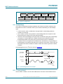
1
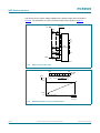
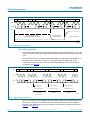
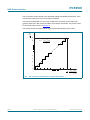
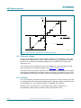
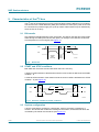
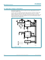
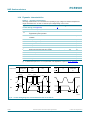
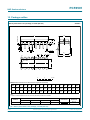
PCF8591 8-bit A/D and D/A converter Rev. 7 — 27 June 2013 Product data sheet 1. General description The PCF8591 is a single-chip, single-supply low-power 8-bit CMOS data acquisition device with four analog inputs, one analog output and a serial I2C-bus interface. Three address pins A0, A1 and A2 are used for programming the hardware address, allowing the use of up to eight devices connected to the I2C-bus without additional hardware. Address, control and data to and from the device are transferred serially via the two-line bidirectional I2C-bus. The functions of the device include analog input multiplexing, on-chip track and hold function, 8-bit analog-to-digital conversion and an 8-bit digital-to-analog conversion. The maximum conversion rate is given by the maximum speed of the I2C-bus. 2. Features and benefits Single power supply Operating supply voltage 2.5 V to 6.0 V Low standby current Serial input and output via I2C-bus I2C address selection by 3 hardware address pins Max sampling rate given by I2C-bus speed 4 analog inputs configurable as single ended or differential inputs Auto-incremented channel selection Analog voltage range from VSS to VDD On-chip track and hold circuit 8-bit successive approximation A/D conversion Multiplying DAC with one analog output. 3. Applications Supply monitoring Reference setting Analog control loops PCF8591 NXP Semiconductors 8-bit A/D and D/A converter 4. Ordering information Table 1. Ordering information Type number Package Name Description Version PCF8591P DIP16 plastic dual in-line package; 16 leads (300 mil) SOT38-4 PCF8591T SO16 plastic small outline package; 16 leads; body width 7.5 mm SOT162-1 4.1 Ordering options Table 2. Ordering options Product type number Sales item (12NC) Orderable part number IC revision Delivery form PCF8591P 933768130112 PCF8591P,112 1 tube PCF8591T/2 935276541512 PCF8591T/2,512 1 tube, dry pack 935276541518 PCF8591T/2,518 1 tape and reel, dry pack, 13 inch 5. Marking Table 3. PCF8591 Product data sheet Marking codes Type number Marking code PCF8591P PCF8591P PCF8591T PCF8591T All information provided in this document is subject to legal disclaimers. Rev. 7 — 27 June 2013 © NXP B.V. 2013. All rights reserved. 2 of 31 PCF8591 NXP Semiconductors 8-bit A/D and D/A converter 6. Block diagram SCL SDA A0 A1 A2 I2C BUS INTERFACE STATUS REGISTER PCF8591 DAC DATA REGISTER ADC DATA REGISTER EXT VDD VSS POWER ON RESET CONTROL LOGIC OSCILLATOR OSC AIN0 AIN1 AIN2 AIN3 ANALOGUE MULTIPLEXER SAMPLE AND HOLD COMPARATOR SAMPLE AND HOLD AOUT SUCCESSIVE APPROXIMATION REGISTER/LOGIC VREF DAC AGND mbl821 Fig 1. Block diagram of PCF8591 7. Pinning information 7.1 Pinning $,1 9'' $,1 9'' $,1 $287 $,1 $287 $,1 95() $,1 95() $*1' $,1 $,1 $ 3&)3 $ 26& $ 26& $ 6&/ $ 6&/ 966 6'$ 966 6'$ Product data sheet Pin configuration for PCF8591P (DIP16) Top view. For mechanical details, see Figure 23 on page 22. Fig 3. All information provided in this document is subject to legal disclaimers. Rev. 7 — 27 June 2013 (;7 DDD Top view. For mechanical details, see Figure 22 on page 21. PCF8591 $*1' $ DDD Fig 2. 3&)7 (;7 Pin configuration for PCF8591T (SO16) © NXP B.V. 2013. All rights reserved. 3 of 31 PCF8591 NXP Semiconductors 8-bit A/D and D/A converter 7.2 Pin description Table 4. PCF8591 Product data sheet Pin description Symbol Pin Description AIN0 1 analog inputs (A/D converter) AIN1 2 AIN2 3 AIN3 4 A0 5 A1 6 A2 7 VSS 8 ground supply voltage SDA 9 I2C-bus serial data input and output SCL 10 I2C-bus serial clock input OSC 11 oscillator input/output EXT 12 external/internal switch for oscillator input AGND 13 analog ground supply VREF 14 voltage reference input AOUT 15 analog output (D/A converter) VDD 16 supply voltage hardware slave address All information provided in this document is subject to legal disclaimers. Rev. 7 — 27 June 2013 © NXP B.V. 2013. All rights reserved. 4 of 31 PCF8591 NXP Semiconductors 8-bit A/D and D/A converter 8. Functional description 8.1 Addressing Each PCF8591 device in an I2C-bus system is activated by sending a valid address to the device. The address consists of a fixed part and a programmable part. The programmable part must be set according to the address pins A0, A1 and A2. The address is always sent as the first byte after the start condition in the I2C-bus protocol. The last bit of the address byte is the read/write-bit which sets the direction of the following data transfer (see Table 5 on page 13, Figure 15 on page 13 and Figure 16 on page 13). 8.2 Control byte The second byte sent to a PCF8591 device is stored in its control register and is required to control the device function. The upper nibble of the control register is used for enabling the analog output, and for programming the analog inputs as single-ended or differential inputs. The lower nibble selects one of the analog input channels defined by the upper nibble (see Figure 4). If the auto-increment flag is set, the channel number is incremented automatically after each A/D conversion. If the auto-increment mode is desired in applications where the internal oscillator is used, the analog output enable flag must be set in the control byte (bit 6). This allows the internal oscillator to run continuously, by this means preventing conversion errors resulting from oscillator start-up delay. The analog output enable flag can be reset at other times to reduce quiescent power consumption. The selection of a non-existing input channel results in the highest available channel number being allocated. Therefore, if the auto-increment flag is set, the next selected channel is always channel 0. The most significant bits of both nibbles are reserved for possible future functions and must be set to logic 0. After a Power-On Reset (POR) condition, all bits of the control register are reset to logic 0. The D/A converter and the oscillator are disabled for power saving. The analog output is switched to a high-impedance state. PCF8591 Product data sheet All information provided in this document is subject to legal disclaimers. Rev. 7 — 27 June 2013 © NXP B.V. 2013. All rights reserved. 5 of 31 PCF8591 NXP Semiconductors 8-bit A/D and D/A converter 06% /6% ; ; ; ; ; ; &21752/%<7( $'&+$11(/180%(5 FKDQQHO FKDQQHO FKDQQHO FKDQQHO $872,1&5(0(17)/$* DFWLYHLI $1$/2*,1387352*5$00,1* IRXUVLQJOHHQGHGLQSXWV $,1FKDQQHO $,1FKDQQHO $,1FKDQQHO $,1FKDQQHO WKUHHGLIIHUHQWLDOLQSXWV $,1 FKDQQHO $,1 FKDQQHO $,1 FKDQQHO $,1 VLQJOHHQGHGDQGGLIIHUHQWLDOPL[HG $,1FKDQQHO $,1FKDQQHO $,1 FKDQQHO $,1 WZRGLIIHUHQWLDOLQSXWV $,1 FKDQQHO $,1 $,1 FKDQQHO $,1 $1$/2*287387(1$%/()/$* DQDORJRXWSXWDFWLYHLI DDD Fig 4. Control byte 8.3 D/A conversion The third byte sent to a PCF8591 device is stored in the DAC data register and is converted to the corresponding analog voltage using the on-chip D/A converter. This D/A converter consists of a resistor divider chain connected to the external reference voltage with 256 taps and selection switches. The tap-decoder switches one of these taps to the DAC output line (see Figure 5). The analog output voltage is buffered by an auto-zeroed unity gain amplifier. Setting the analog output enable flag of the control register switches this buffer amp on or off. In the active state, the output voltage is held until a further data byte is sent. The on-chip D/A converter is also used for successive approximation A/D conversion. In order to release the DAC for an A/D conversion cycle the unity gain amplifier is equipped with a track and hold circuit. This circuit holds the output voltage while executing the A/D conversion. PCF8591 Product data sheet All information provided in this document is subject to legal disclaimers. Rev. 7 — 27 June 2013 © NXP B.V. 2013. All rights reserved. 6 of 31 PCF8591 NXP Semiconductors 8-bit A/D and D/A converter The formula for the output voltage supplied to the analog output AOUT is shown in Figure 6. The waveforms of a D/A conversion sequence are shown in Figure 7. '$&RXW 95() 5 )) 5 ' ' 5 7$3 '(&2'(5 5 ' 5 $*1' DDD Fig 5. DAC resistor divider chain 06% ' 9$287 9'' /6% ' ' ' ' ' ' ' '$&GDWD UHJLVWHU 995()9$*1' 9$287 9$*1''LîL L 995() 9$*1' 966 )( )) '$&KH[ DDD Fig 6. PCF8591 Product data sheet DAC data and DC conversion characteristics All information provided in this document is subject to legal disclaimers. Rev. 7 — 27 June 2013 © NXP B.V. 2013. All rights reserved. 7 of 31 PCF8591 NXP Semiconductors 8-bit A/D and D/A converter SURWRFRO $''5(66 6 6&/ $ &21752/%<7( $ '$7$%<7( $ '$7$%<7( $ 6'$ 9$287 KLJKLPSHGDQFHVWDWHRI SUHYLRXVYDOXHKHOGLQ'$&UHJLVWHU SUHYLRXVYDOXHKHOG LQ'$&UHJLVWHU YDOXHRIGDWDE\WH WLPH DDD Fig 7. D/A conversion sequence 8.4 A/D conversion The A/D converter uses the successive approximation conversion technique. The on-chip D/A converter and a high-gain comparator are used temporarily during an A/D conversion cycle. An A/D conversion cycle is always started after sending a valid read mode address to a PCF8591 device. The A/D conversion cycle is triggered at the trailing edge of the acknowledge clock pulse and is executed while transmitting the result of the previous conversion (see Figure 8). protocol S ADDRESS 1 A DATA BYTE 0 A DATA BYTE 1 A DATA BYTE 2 A SCL 1 2 8 9 1 9 1 9 1 SDA Fig 8. sampling byte 1 sampling byte 2 sampling byte 3 conversion of byte 1 conversion of byte 2 conversion of byte 3 transmission of previously converted byte transmission of byte 1 transmission of byte 2 mbl829 A/D conversion sequence Once a conversion cycle is triggered, an input voltage sample of the selected channel is stored on the chip and is converted to the corresponding 8-bit binary code. Samples picked up from differential inputs are converted to an 8-bit two's complement code (see Figure 9 and Figure 10). PCF8591 Product data sheet All information provided in this document is subject to legal disclaimers. Rev. 7 — 27 June 2013 © NXP B.V. 2013. All rights reserved. 8 of 31 PCF8591 NXP Semiconductors 8-bit A/D and D/A converter The conversion result is stored in the ADC data register and awaits transmission. If the auto-increment flag is set, the next channel is selected. The first byte transmitted in a read cycle contains the conversion result code of the previous read cycle. After a POR condition, the first byte read is 80h. The protocol of an I2C-bus read cycle is shown in Section 9. The maximum A/D conversion rate is given by the actual speed of the I2C-bus. HEX code FF FE Vlsb = VREF − VAGND 256 04 03 02 01 00 0 1 2 3 4 254 255 VAIN − VAGND Vlsb mbl830 Fig 9. PCF8591 Product data sheet A/D conversion characteristics of single ended inputs All information provided in this document is subject to legal disclaimers. Rev. 7 — 27 June 2013 © NXP B.V. 2013. All rights reserved. 9 of 31 PCF8591 NXP Semiconductors 8-bit A/D and D/A converter HEX CODE 7F 7E 02 01 00 −128 −127 −2 −1 0 1 2 126 127 VAIN + − VAIN − FF Vlsb FE Vlsb = VREF − VAGND 256 81 80 mbl831 Fig 10. A/D conversion characteristics of differential inputs 8.5 Reference voltage For the D/A and A/D conversion, either a stable external voltage reference or the supply voltage must be applied to the resistor divider chain (pins VREF and AGND). The AGND pin has to be connected to the system analog ground. It may have a DC off-set with reference to VSS. A low frequency can be applied to the VREF and AGND pins. This allows the use of the D/A converter as a one-quadrant multiplier (see Section 10 and Figure 6) The A/D converter can also be used as a one or two quadrant analog divider. The analog input voltage is divided by the reference voltage. The result is converted to a binary code. In this application, the reference voltage must be kept stable during the conversion cycle. 8.6 Oscillator An on-chip oscillator generates the clock signal required for the A/D conversion cycle and for refreshing the auto-zeroed buffer amplifier. When using this oscillator the EXT pin must be connected to VSS. The oscillator frequency is available at the OSC pin. If the EXT pin is connected to VDD, the oscillator output OSC is switched to a high-impedance state allowing to feed an external clock signal to OSC. PCF8591 Product data sheet All information provided in this document is subject to legal disclaimers. Rev. 7 — 27 June 2013 © NXP B.V. 2013. All rights reserved. 10 of 31 PCF8591 NXP Semiconductors 8-bit A/D and D/A converter 9. Characteristics of the I2C bus The I2C-bus is for bidirectional, two-line communication between different ICs or modules. The two lines are a Serial DAta line (SDA) and a Serial CLock line (SCL). Both lines must be connected to a positive supply via a pull-up resistor. Data transfer may be initiated only when the bus is not busy. 9.1 Bit transfer One data bit is transferred during each clock pulse. The data on the SDA line must remain stable during the HIGH period of the clock pulse, as changes in the data line at this time are interpreted as a control signal (see Figure 11). SDA SCL data line stable; data valid change of data allowed mbc621 Fig 11. Bit transfer 9.2 START and STOP conditions Both data and clock lines remain HIGH when the bus is not busy. A HIGH-to-LOW transition of the data line while the clock is HIGH is defined as the START condition - S. A LOW-to-HIGH transition of the data line while the clock is HIGH is defined as the STOP condition - P (see Figure 12). SDA SDA SCL SCL S P START condition STOP condition mbc622 Fig 12. Definition of START and STOP conditions 9.3 System configuration A device generating a message is a transmitter; a device receiving a message is a receiver. The device that controls the message is the master; and the devices which are controlled by the master are the slaves (see Figure 13). PCF8591 Product data sheet All information provided in this document is subject to legal disclaimers. Rev. 7 — 27 June 2013 © NXP B.V. 2013. All rights reserved. 11 of 31 PCF8591 NXP Semiconductors 8-bit A/D and D/A converter MASTER TRANSMITTER/ RECEIVER SLAVE TRANSMITTER/ RECEIVER SLAVE RECEIVER MASTER TRANSMITTER/ RECEIVER MASTER TRANSMITTER SDA SCL mga807 Fig 13. System configuration 9.4 Acknowledge The number of data bytes transferred between the START and STOP conditions from transmitter to receiver is unlimited. Each byte of 8 bits is followed by an acknowledge cycle. • A slave receiver, which is addressed, must generate an acknowledge after the reception of each byte • Also a master receiver must generate an acknowledge after the reception of each byte that has been clocked out of the slave transmitter • The device that acknowledges must pull-down the SDA line during the acknowledge clock pulse, so that the SDA line is stable LOW during the HIGH period of the acknowledge related clock pulse (set-up and hold times must be considered) • A master receiver must signal an end of data to the transmitter by not generating an acknowledge on the last byte that has been clocked out of the slave. In this event, the transmitter must leave the data line HIGH to enable the master to generate a STOP condition Acknowledgement on the I2C-bus is shown in Figure 14. data output by transmitter not acknowledge data output by receiver acknowledge SCL from master 1 2 8 9 S START condition clock pulse for acknowledgement mbc602 Fig 14. Acknowledgement on the I2C-bus 9.5 I2C bus protocol After a START condition, the I2C slave address has to be sent to the PCF8591 device. PCF8591 Product data sheet All information provided in this document is subject to legal disclaimers. Rev. 7 — 27 June 2013 © NXP B.V. 2013. All rights reserved. 12 of 31 PCF8591 NXP Semiconductors 8-bit A/D and D/A converter Eight different I2C-bus slave addresses can be used to address the PCF8591 (see Table 5). Table 5. I2C slave address byte Slave address Bit 7 6 5 4 3 2 1 0 0 1 A2 A1 A0 0 MSB slave address LSB 1 R/W The least significant bit of the slave address byte is bit R/W (see Table 6). Table 6. R/W-bit description R/W Description 0 write data 1 read data Bit 1 to bit 3 of the slave address are defined by connecting the input pins A0 to A2 to either VSS (logic 0) or VDD (logic 1). Therefore, eight instances of PCF8591 can be distinguished on the same I2C-bus. acknowledge from PCF8591 acknowledge from PCF8591 S ADDRESS 0 A CONTROL BYTE A acknowledge from PCF8591 DATA BYTE A P/S N = 0 to M data bytes mbl833 Fig 15. Bus protocol for write mode, D/A conversion acknowledge from master acknowledge from PCF8591 S ADDRESS 1 A DATA BYTE N = 0 to M data bytes A no acknowledge LAST DATA BYTE 1 P mbl834 Fig 16. Bus protocol for read mode, A/D conversion PCF8591 Product data sheet All information provided in this document is subject to legal disclaimers. Rev. 7 — 27 June 2013 © NXP B.V. 2013. All rights reserved. 13 of 31 PCF8591 NXP Semiconductors 8-bit A/D and D/A converter 10. Application design-in information Inputs must be connected to VSS or VDD when not in use. Analog inputs may also be connected to AGND or VREF. In order to prevent excessive ground and supply noise and to minimize crosstalk of the digital to analog signal paths the printed-circuit board layout must be very carefully designed. Supply lines common to a PCF8591 device and noisy digital circuits and ground loops should be avoided. Decoupling capacitors (>10 F) are recommended for power supply and reference voltage inputs. VDD VDD VDD V0 VDD AOUT AIN0 AIN1 VREF AIN2 AGND AIN3 EXT A0 OSC PCF8591 A1 SCL A2 SDA VSS VDD +θ +θ VOUT VDD V0 V1 VDD VDD AOUT AIN0 AIN1 VREF AIN2 AGND AIN3 EXT A0 OSC PCF8591 SCL A1 A2 SDA VSS VOUT V2 VDD MASTER TRANSMITTER ANALOGUE GROUND DIGITAL GROUND I2C bus mbl839 Fig 17. Application diagram PCF8591 Product data sheet All information provided in this document is subject to legal disclaimers. Rev. 7 — 27 June 2013 © NXP B.V. 2013. All rights reserved. 14 of 31 PCF8591 NXP Semiconductors 8-bit A/D and D/A converter 11. Internal circuitry 3&) $,1 VXEVWUDWH 9'' $287 $,1 95() $,1 $*1' $,1 (;7 $ 26& $ 6&/ $ 6'$ 966 DDD Fig 18. Device protection diagram 12. Safety notes CAUTION This device is sensitive to ElectroStatic Discharge (ESD). Observe precautions for handling electrostatic sensitive devices. Such precautions are described in the ANSI/ESD S20.20, IEC/ST 61340-5, JESD625-A or equivalent standards. PCF8591 Product data sheet All information provided in this document is subject to legal disclaimers. Rev. 7 — 27 June 2013 © NXP B.V. 2013. All rights reserved. 15 of 31 PCF8591 NXP Semiconductors 8-bit A/D and D/A converter 13. Limiting values Table 7. Limiting values In accordance with the Absolute Maximum Rating System (IEC 60134). Symbol Parameter VDD supply voltage Conditions Min Max Unit 0.5 +8.0 V VI input voltage 0.5 VDD + 0.5 V II input current - 10 mA IO output current - 20 mA IDD supply current - 50 mA ISS ground supply current - 50 mA Ptot total power dissipation per package - 300 mW P/out power dissipation per output - 100 mW VESD electrostatic discharge voltage Ilu latch-up current Tamb ambient temperature any input HBM [1] - 3000 V MM [2] - 300 V [3] - 200 mA 40 +85 C 65 +150 C operating device [4] storage temperature Tstg [1] Pass level; Human Body Model (HBM), according to Ref. 6 “JESD22-A114”. [2] Pass level; Machine Model (MM), according to Ref. 7 “JESD22-A115”. [3] Pass level; latch-up testing according to Ref. 8 “JESD78” at maximum ambient temperature (Tamb(max)). [4] According to the store and transport requirements (see Ref. 12 “UM10569”) the devices have to be stored at a temperature of +8 C to +45 C and a humidity of 25 % to 75 %. PCF8591 Product data sheet All information provided in this document is subject to legal disclaimers. Rev. 7 — 27 June 2013 © NXP B.V. 2013. All rights reserved. 16 of 31 PCF8591 NXP Semiconductors 8-bit A/D and D/A converter 14. Characteristics 14.1 Static characteristics Table 8. Characteristics VDD = 2.5 V to 6.0 V; VSS = 0; Tamb = 40 oC to +85 oC unless otherwise specified. Symbol Parameter Conditions Min Typ Max Unit 2.5 - 6.0 V - 1 15 A - 125 250 A - 0.45 1.0 mA 0.8 - 2.0 V Supply VDD supply voltage IDD supply current standby; VI = VSS or VDD; no load operating; fSCL = 100 kHz AOUT off AOUT active VPOR [1] power-on reset voltage Digital in- and outputs: SCL, SDA, A0, A1, A2 VIL LOW-level input voltage 0 - 0.3 VDD V VIH HIGH-level input voltage 0.7 VDD - VDD V IL leakage current A0, A1, A2 250 - +250 nA SCL, SDA 1 - +1 A - - 5 pF 3.0 - - mA Ci input capacitance IOL LOW-level output current VI = VSS to VDD VOL = 0.4 V Reference voltage inputs reference voltage Vref VAGND voltage on pin AGND ILI input leakage current Rref reference resistance Vref > VAGND [2] VSS + 1.6 - VDD V Vref > VAGND [2] VSS - VDD 0.8 V 250 - +250 nA - 100 - k pins VREF and AGND Oscillator: OSC, EXT ILI input leakage current - - 250 nA fOSC oscillator frequency 0.75 - 1.25 MHz [1] The power-on reset circuit resets the I2C-bus logic when VDD is less than VPOR. [2] A further extension of the range is possible, if the following conditions are fulfilled: --------------------------------- 0.8 V , V ref + V AGND 2 V ref + V AGND V DD – --------------------------------- 0.4 V . 2 PCF8591 Product data sheet All information provided in this document is subject to legal disclaimers. Rev. 7 — 27 June 2013 © NXP B.V. 2013. All rights reserved. 17 of 31 PCF8591 NXP Semiconductors 8-bit A/D and D/A converter 14.2 D/A characteristics Table 9. D/A characteristics VDD = 5.0 V; VSS = 0; VREF =5.0 V; VAGND = 0 V; RL = 10 k; CL = 100 pF; Tamb = 40 oC to +85 oC unless otherwise specified. Symbol Parameter Conditions Min Typ Max Unit no resistive load VSS - VDD V RL = 10 k VSS - 0.9 VDD V - - 250 nA - - 50 mV - - 1.5 LSB Analog output Voa ILO analog output voltage output leakage current AOUT disabled Accuracy Tamb = 25 oC EO offset error EL linearity error EG gain error no resistive load - - 1 % to 1/2 LSB full scale ts(DAC) DAC settling time - - 90 s fc(DAC) DAC conversion frequency - - 11.1 kHz SNRR supply noise rejection f = 100 Hz; ratio VDDN = 0.1 VPP - 40 - dB 14.3 A/D characteristics Table 10. A/D characteristics VDD = 5.0 V; VSS = 0; VREF =5.0 V; VAGND = 0 V; RS = 10 k; Tamb = 40 oC to +85 oC unless otherwise specified. Symbol Parameter Conditions Min Typ Max Unit Analog inputs Via analog input voltage VSS - VDD V ILIA analog input leakage current - - 100 nA Ci(a) analog input capacitance - 10 - pF Ci(dif) differential input capacitance - 10 - pF Vi(se) single-ended input voltage measuring range VAGND - VREF V Vi(dif) differential input voltage measuring range: – V FS -----------2 - +V FS -----------2 V VFS = VREF - VAGND EO offset error Tamb = 25 oC - - 20 mV EL linearity error - - 1.5 LSB EG gain error - - 1 % - - 5 % - 60 - dB Accuracy small signal; Vi = 16 LSB CMRR common mode rejection ratio PCF8591 Product data sheet All information provided in this document is subject to legal disclaimers. Rev. 7 — 27 June 2013 © NXP B.V. 2013. All rights reserved. 18 of 31 PCF8591 NXP Semiconductors 8-bit A/D and D/A converter Table 10. A/D characteristics …continued VDD = 5.0 V; VSS = 0; VREF =5.0 V; VAGND = 0 V; RS = 10 k; Tamb = 40 oC to +85 oC unless otherwise specified. Symbol Parameter SNRR Conditions Min Typ Max Unit supply noise rejection f = 100 Hz; ratio VDDN = 0.1 VPP - 40 - dB tconv conversion time - - 90 s fs sampling frequency - - 11.1 kHz DDD ,'' $ DDD ,'' $ & & & 9''9 a. internal oscillator; Tamb = +27 C 9''9 b. External oscillator Fig 19. Operating supply current as a function of supply voltage (analog output disabled) DDD '$RXWSXW LPSHGDQFH K K K K K KH[LQSXWFRGH DDD '$RXWSXW LPSHGDQFH $K a. Output impedance near negative power rail; Tamb = +27 C %K &K 'K (K )K KH[LQSXWFRGH ))K b. Output impedance near positive power rail; Tamb = +27 C Fig 20. Output impedance of analog output buffer (near power rails) PCF8591 Product data sheet All information provided in this document is subject to legal disclaimers. Rev. 7 — 27 June 2013 © NXP B.V. 2013. All rights reserved. 19 of 31 PCF8591 NXP Semiconductors 8-bit A/D and D/A converter 14.4 Dynamic characteristics Table 11. Dynamic characteristics All timing characteristics are valid within the operating supply voltage and ambient temperature range and reference to VIL and VIH with an input voltage swing of VSS to VDD. Symbol Parameter I2C Typ Max Unit bus timing (see Figure 21) fSCL SCL clock frequency - - 100 kHz tSP pulse width of spikes that must be suppressed by the input filter - - 100 ns tBUF bus free time between a STOP and START condition 4.7 - - s tSU;STA set-up time for a repeated START condition 4.7 - - s tHD;STA hold time (repeated) START condition 4.0 - - s tLOW LOW period of the SCL clock 4.7 - - s tHIGH HIGH period of the SCL clock 4.0 - - s tr rise time of both SDA and SCL signals - - 1.0 s tf fall time of both SDA and SCL signals - - 0.3 s tSU;DAT data set-up time 250 - - s tHD;DAT data hold time 0 - - s tVD;DAT data valid time - - 3.4 s tSU;STO set-up time for STOP condition 4.0 - - s [1] PROTOCOL Min [1] A detailed description of the I2C bus specification, with applications, is given in Ref. 11 “UM10204”. tSU;STA BIT 6 (A6) BIT 7 MSB (A7) START CONDITION (S) tLOW tHIGH BIT 0 LSB (R/W) ACKNOWLEDGE (A) STOP CONDITION (P) 1 / fSCL SCL tBUF tr tf SDA tHD;STA tSU;DAT tHD;DAT tVD;DAT tSU;STO mbd820 Fig 21. I2C bus timing diagram; rise and fall times refer to VIL and VIH PCF8591 Product data sheet All information provided in this document is subject to legal disclaimers. Rev. 7 — 27 June 2013 © NXP B.V. 2013. All rights reserved. 20 of 31 PCF8591 NXP Semiconductors 8-bit A/D and D/A converter 15. Package outline DIP16: plastic dual in-line package; 16 leads (300 mil) SOT38-4 ME seating plane D A2 A A1 L c e Z w M b1 (e 1) b b2 MH 9 16 pin 1 index E 1 8 0 5 10 mm scale DIMENSIONS (inch dimensions are derived from the original mm dimensions) UNIT A max. A1 min. A2 max. b b1 b2 c D (1) E (1) e e1 L ME MH w Z (1) max. mm 4.2 0.51 3.2 1.73 1.30 0.53 0.38 1.25 0.85 0.36 0.23 19.50 18.55 6.48 6.20 2.54 7.62 3.60 3.05 8.25 7.80 10.0 8.3 0.254 0.76 inches 0.17 0.02 0.13 0.068 0.051 0.021 0.015 0.049 0.033 0.014 0.009 0.77 0.73 0.26 0.24 0.1 0.3 0.14 0.12 0.32 0.31 0.39 0.33 0.01 0.03 Note 1. Plastic or metal protrusions of 0.25 mm (0.01 inch) maximum per side are not included. OUTLINE VERSION REFERENCES IEC JEDEC JEITA EUROPEAN PROJECTION ISSUE DATE 95-01-14 03-02-13 SOT38-4 Fig 22. DIP16: plastic dual in-line package; 16 leads (300 mil) PCF8591 Product data sheet All information provided in this document is subject to legal disclaimers. Rev. 7 — 27 June 2013 © NXP B.V. 2013. All rights reserved. 21 of 31 PCF8591 NXP Semiconductors 8-bit A/D and D/A converter SO16: plastic small outline package; 16 leads; body width 7.5 mm SOT162-1 D E A X c HE y v M A Z 9 16 Q A2 A (A 3) A1 pin 1 index θ Lp L 1 8 e detail X w M bp 0 5 10 mm scale DIMENSIONS (inch dimensions are derived from the original mm dimensions) UNIT A max. A1 A2 A3 bp c D (1) E (1) e HE L Lp Q v w y mm 2.65 0.3 0.1 2.45 2.25 0.25 0.49 0.36 0.32 0.23 10.5 10.1 7.6 7.4 1.27 10.65 10.00 1.4 1.1 0.4 1.1 1.0 0.25 0.25 0.1 0.01 0.019 0.013 0.014 0.009 0.41 0.40 0.30 0.29 0.05 0.419 0.043 0.055 0.394 0.016 inches 0.1 0.012 0.096 0.004 0.089 0.043 0.039 0.01 0.01 Z (1) 0.9 0.4 0.035 0.004 0.016 θ 8o o 0 Note 1. Plastic or metal protrusions of 0.15 mm (0.006 inch) maximum per side are not included. REFERENCES OUTLINE VERSION IEC JEDEC SOT162-1 075E03 MS-013 JEITA EUROPEAN PROJECTION ISSUE DATE 99-12-27 03-02-19 Fig 23. SO16: plastic small outline package; 16 leads: body width 7.5 mm PCF8591 Product data sheet All information provided in this document is subject to legal disclaimers. Rev. 7 — 27 June 2013 © NXP B.V. 2013. All rights reserved. 22 of 31 PCF8591 NXP Semiconductors 8-bit A/D and D/A converter 16. Soldering of SMD packages This text provides a very brief insight into a complex technology. A more in-depth account of soldering ICs can be found in Application Note AN10365 “Surface mount reflow soldering description”. 16.1 Introduction to soldering Soldering is one of the most common methods through which packages are attached to Printed Circuit Boards (PCBs), to form electrical circuits. The soldered joint provides both the mechanical and the electrical connection. There is no single soldering method that is ideal for all IC packages. Wave soldering is often preferred when through-hole and Surface Mount Devices (SMDs) are mixed on one printed wiring board; however, it is not suitable for fine pitch SMDs. Reflow soldering is ideal for the small pitches and high densities that come with increased miniaturization. 16.2 Wave and reflow soldering Wave soldering is a joining technology in which the joints are made by solder coming from a standing wave of liquid solder. The wave soldering process is suitable for the following: • Through-hole components • Leaded or leadless SMDs, which are glued to the surface of the printed circuit board Not all SMDs can be wave soldered. Packages with solder balls, and some leadless packages which have solder lands underneath the body, cannot be wave soldered. Also, leaded SMDs with leads having a pitch smaller than ~0.6 mm cannot be wave soldered, due to an increased probability of bridging. The reflow soldering process involves applying solder paste to a board, followed by component placement and exposure to a temperature profile. Leaded packages, packages with solder balls, and leadless packages are all reflow solderable. Key characteristics in both wave and reflow soldering are: • • • • • • Board specifications, including the board finish, solder masks and vias Package footprints, including solder thieves and orientation The moisture sensitivity level of the packages Package placement Inspection and repair Lead-free soldering versus SnPb soldering 16.3 Wave soldering Key characteristics in wave soldering are: • Process issues, such as application of adhesive and flux, clinching of leads, board transport, the solder wave parameters, and the time during which components are exposed to the wave • Solder bath specifications, including temperature and impurities PCF8591 Product data sheet All information provided in this document is subject to legal disclaimers. Rev. 7 — 27 June 2013 © NXP B.V. 2013. All rights reserved. 23 of 31 PCF8591 NXP Semiconductors 8-bit A/D and D/A converter 16.4 Reflow soldering Key characteristics in reflow soldering are: • Lead-free versus SnPb soldering; note that a lead-free reflow process usually leads to higher minimum peak temperatures (see Figure 24) than a SnPb process, thus reducing the process window • Solder paste printing issues including smearing, release, and adjusting the process window for a mix of large and small components on one board • Reflow temperature profile; this profile includes preheat, reflow (in which the board is heated to the peak temperature) and cooling down. It is imperative that the peak temperature is high enough for the solder to make reliable solder joints (a solder paste characteristic). In addition, the peak temperature must be low enough that the packages and/or boards are not damaged. The peak temperature of the package depends on package thickness and volume and is classified in accordance with Table 12 and 13 Table 12. SnPb eutectic process (from J-STD-020D) Package thickness (mm) Package reflow temperature (C) Volume (mm3) < 350 350 < 2.5 235 220 2.5 220 220 Table 13. Lead-free process (from J-STD-020D) Package thickness (mm) Package reflow temperature (C) Volume (mm3) < 350 350 to 2000 > 2000 < 1.6 260 260 260 1.6 to 2.5 260 250 245 > 2.5 250 245 245 Moisture sensitivity precautions, as indicated on the packing, must be respected at all times. Studies have shown that small packages reach higher temperatures during reflow soldering, see Figure 24. PCF8591 Product data sheet All information provided in this document is subject to legal disclaimers. Rev. 7 — 27 June 2013 © NXP B.V. 2013. All rights reserved. 24 of 31 PCF8591 NXP Semiconductors 8-bit A/D and D/A converter temperature maximum peak temperature = MSL limit, damage level minimum peak temperature = minimum soldering temperature peak temperature time 001aac844 MSL: Moisture Sensitivity Level Fig 24. Temperature profiles for large and small components For further information on temperature profiles, refer to Application Note AN10365 “Surface mount reflow soldering description”. 17. References [1] AN10365 — Surface mount reflow soldering description [2] AN10853 — ESD and EMC sensitivity of IC [3] IEC 60134 — Rating systems for electronic tubes and valves and analogous semiconductor devices [4] IEC 61340-5 — Protection of electronic devices from electrostatic phenomena [5] IPC/JEDEC J-STD-020D — Moisture/Reflow Sensitivity Classification for Nonhermetic Solid State Surface Mount Devices [6] JESD22-A114 — Electrostatic Discharge (ESD) Sensitivity Testing Human Body Model (HBM) [7] JESD22-A115 — Electrostatic Discharge (ESD) Sensitivity Testing Machine Model (MM) [8] JESD78 — IC Latch-Up Test [9] JESD625-A — Requirements for Handling Electrostatic-Discharge-Sensitive (ESDS) Devices [10] SNV-FA-01-02 — Marking Formats Integrated Circuits [11] UM10204 — I2C-bus specification and user manual [12] UM10569 — Store and transport requirements PCF8591 Product data sheet All information provided in this document is subject to legal disclaimers. Rev. 7 — 27 June 2013 © NXP B.V. 2013. All rights reserved. 25 of 31 PCF8591 NXP Semiconductors 8-bit A/D and D/A converter 18. Revision history Table 14. Revision history Document ID Release date Data sheet status Change notice Supersedes PCF8591 v.7 20130627 Product data sheet - PCF8591 v.6 Modifications: • The format of this data sheet has been redesigned to comply with the new identity guidelines of NXP Semiconductors. • Legal texts have been adapted to the new company name where appropriate. PCF8591 v.6 20030127 Product data sheet PCF8591 v.5 20011213 Product data sheet - PCF8591 v.4 PCF8591 v.4 19980702 Product data sheet - PCF8591 v.3 PCF8591 v.3 19970402 Product data sheet - PCF8591 v.2 PCF8591 v.2 19910901 Product data sheet - PCF8591 v.1 PCF8591 v.1 19860627 Product data sheet - - PCF8591 Product data sheet - All information provided in this document is subject to legal disclaimers. Rev. 7 — 27 June 2013 PCF8591 v.5 © NXP B.V. 2013. All rights reserved. 26 of 31 PCF8591 NXP Semiconductors 8-bit A/D and D/A converter 19. Legal information 19.1 Data sheet status Document status[1][2] Product status[3] Definition Objective [short] data sheet Development This document contains data from the objective specification for product development. Preliminary [short] data sheet Qualification This document contains data from the preliminary specification. Product [short] data sheet Production This document contains the product specification. [1] Please consult the most recently issued document before initiating or completing a design. [2] The term ‘short data sheet’ is explained in section “Definitions”. [3] The product status of device(s) described in this document may have changed since this document was published and may differ in case of multiple devices. The latest product status information is available on the Internet at URL http://www.nxp.com. 19.2 Definitions Draft — The document is a draft version only. The content is still under internal review and subject to formal approval, which may result in modifications or additions. NXP Semiconductors does not give any representations or warranties as to the accuracy or completeness of information included herein and shall have no liability for the consequences of use of such information. Short data sheet — A short data sheet is an extract from a full data sheet with the same product type number(s) and title. A short data sheet is intended for quick reference only and should not be relied upon to contain detailed and full information. For detailed and full information see the relevant full data sheet, which is available on request via the local NXP Semiconductors sales office. In case of any inconsistency or conflict with the short data sheet, the full data sheet shall prevail. Product specification — The information and data provided in a Product data sheet shall define the specification of the product as agreed between NXP Semiconductors and its customer, unless NXP Semiconductors and customer have explicitly agreed otherwise in writing. In no event however, shall an agreement be valid in which the NXP Semiconductors product is deemed to offer functions and qualities beyond those described in the Product data sheet. 19.3 Disclaimers Limited warranty and liability — Information in this document is believed to be accurate and reliable. However, NXP Semiconductors does not give any representations or warranties, expressed or implied, as to the accuracy or completeness of such information and shall have no liability for the consequences of use of such information. NXP Semiconductors takes no responsibility for the content in this document if provided by an information source outside of NXP Semiconductors. In no event shall NXP Semiconductors be liable for any indirect, incidental, punitive, special or consequential damages (including - without limitation - lost profits, lost savings, business interruption, costs related to the removal or replacement of any products or rework charges) whether or not such damages are based on tort (including negligence), warranty, breach of contract or any other legal theory. Notwithstanding any damages that customer might incur for any reason whatsoever, NXP Semiconductors’ aggregate and cumulative liability towards customer for the products described herein shall be limited in accordance with the Terms and conditions of commercial sale of NXP Semiconductors. Right to make changes — NXP Semiconductors reserves the right to make changes to information published in this document, including without limitation specifications and product descriptions, at any time and without notice. This document supersedes and replaces all information supplied prior to the publication hereof. PCF8591 Product data sheet Suitability for use — NXP Semiconductors products are not designed, authorized or warranted to be suitable for use in life support, life-critical or safety-critical systems or equipment, nor in applications where failure or malfunction of an NXP Semiconductors product can reasonably be expected to result in personal injury, death or severe property or environmental damage. NXP Semiconductors and its suppliers accept no liability for inclusion and/or use of NXP Semiconductors products in such equipment or applications and therefore such inclusion and/or use is at the customer’s own risk. Applications — Applications that are described herein for any of these products are for illustrative purposes only. NXP Semiconductors makes no representation or warranty that such applications will be suitable for the specified use without further testing or modification. Customers are responsible for the design and operation of their applications and products using NXP Semiconductors products, and NXP Semiconductors accepts no liability for any assistance with applications or customer product design. It is customer’s sole responsibility to determine whether the NXP Semiconductors product is suitable and fit for the customer’s applications and products planned, as well as for the planned application and use of customer’s third party customer(s). Customers should provide appropriate design and operating safeguards to minimize the risks associated with their applications and products. NXP Semiconductors does not accept any liability related to any default, damage, costs or problem which is based on any weakness or default in the customer’s applications or products, or the application or use by customer’s third party customer(s). Customer is responsible for doing all necessary testing for the customer’s applications and products using NXP Semiconductors products in order to avoid a default of the applications and the products or of the application or use by customer’s third party customer(s). NXP does not accept any liability in this respect. Limiting values — Stress above one or more limiting values (as defined in the Absolute Maximum Ratings System of IEC 60134) will cause permanent damage to the device. Limiting values are stress ratings only and (proper) operation of the device at these or any other conditions above those given in the Recommended operating conditions section (if present) or the Characteristics sections of this document is not warranted. Constant or repeated exposure to limiting values will permanently and irreversibly affect the quality and reliability of the device. Terms and conditions of commercial sale — NXP Semiconductors products are sold subject to the general terms and conditions of commercial sale, as published at http://www.nxp.com/profile/terms, unless otherwise agreed in a valid written individual agreement. In case an individual agreement is concluded only the terms and conditions of the respective agreement shall apply. NXP Semiconductors hereby expressly objects to applying the customer’s general terms and conditions with regard to the purchase of NXP Semiconductors products by customer. No offer to sell or license — Nothing in this document may be interpreted or construed as an offer to sell products that is open for acceptance or the grant, conveyance or implication of any license under any copyrights, patents or other industrial or intellectual property rights. All information provided in this document is subject to legal disclaimers. Rev. 7 — 27 June 2013 © NXP B.V. 2013. All rights reserved. 27 of 31 PCF8591 NXP Semiconductors 8-bit A/D and D/A converter Export control — This document as well as the item(s) described herein may be subject to export control regulations. Export might require a prior authorization from competent authorities. Non-automotive qualified products — Unless this data sheet expressly states that this specific NXP Semiconductors product is automotive qualified, the product is not suitable for automotive use. It is neither qualified nor tested in accordance with automotive testing or application requirements. NXP Semiconductors accepts no liability for inclusion and/or use of non-automotive qualified products in automotive equipment or applications. In the event that customer uses the product for design-in and use in automotive applications to automotive specifications and standards, customer (a) shall use the product without NXP Semiconductors’ warranty of the product for such automotive applications, use and specifications, and (b) whenever customer uses the product for automotive applications beyond NXP Semiconductors’ specifications such use shall be solely at customer’s own risk, and (c) customer fully indemnifies NXP Semiconductors for any liability, damages or failed product claims resulting from customer design and use of the product for automotive applications beyond NXP Semiconductors’ standard warranty and NXP Semiconductors’ product specifications. Translations — A non-English (translated) version of a document is for reference only. The English version shall prevail in case of any discrepancy between the translated and English versions. 19.4 Trademarks Notice: All referenced brands, product names, service names and trademarks are the property of their respective owners. I2C-bus — logo is a trademark of NXP B.V. 20. Contact information For more information, please visit: http://www.nxp.com For sales office addresses, please send an email to: [email protected] PCF8591 Product data sheet All information provided in this document is subject to legal disclaimers. Rev. 7 — 27 June 2013 © NXP B.V. 2013. All rights reserved. 28 of 31 PCF8591 NXP Semiconductors 8-bit A/D and D/A converter 21. Tables Table 1. Table 2. Table 3. Table 4. Table 5. Table 6. Table 7. Table 8. Table 9. Table 10. Table 11. Table 12. Table 13. Table 14. Ordering information . . . . . . . . . . . . . . . . . . . . .2 Ordering options . . . . . . . . . . . . . . . . . . . . . . . . .2 Marking codes . . . . . . . . . . . . . . . . . . . . . . . . . .2 Pin description . . . . . . . . . . . . . . . . . . . . . . . . . .4 I2C slave address byte . . . . . . . . . . . . . . . . . . .13 R/W-bit description . . . . . . . . . . . . . . . . . . . . . .13 Limiting values . . . . . . . . . . . . . . . . . . . . . . . . .16 Characteristics . . . . . . . . . . . . . . . . . . . . . . . . .17 D/A characteristics . . . . . . . . . . . . . . . . . . . . . .18 A/D characteristics . . . . . . . . . . . . . . . . . . . . . .18 Dynamic characteristics . . . . . . . . . . . . . . . . . .20 SnPb eutectic process (from J-STD-020D) . . .24 Lead-free process (from J-STD-020D) . . . . . .24 Revision history . . . . . . . . . . . . . . . . . . . . . . . .26 PCF8591 Product data sheet All information provided in this document is subject to legal disclaimers. Rev. 7 — 27 June 2013 © NXP B.V. 2013. All rights reserved. 29 of 31 PCF8591 NXP Semiconductors 8-bit A/D and D/A converter 22. Figures Fig 1. Fig 2. Fig 3. Fig 4. Fig 5. Fig 6. Fig 7. Fig 8. Fig 9. Fig 10. Fig 11. Fig 12. Fig 13. Fig 14. Fig 15. Fig 16. Fig 17. Fig 18. Fig 19. Fig 20. Fig 21. Fig 22. Fig 23. Fig 24. Block diagram of PCF8591 . . . . . . . . . . . . . . . . . .3 Pin configuration for PCF8591P (DIP16) . . . . . . . .3 Pin configuration for PCF8591T (SO16) . . . . . . . .3 Control byte . . . . . . . . . . . . . . . . . . . . . . . . . . . . . .6 DAC resistor divider chain . . . . . . . . . . . . . . . . . . .7 DAC data and DC conversion characteristics . . . .7 D/A conversion sequence . . . . . . . . . . . . . . . . . . .8 A/D conversion sequence . . . . . . . . . . . . . . . . . . .8 A/D conversion characteristics of single ended inputs . . . . . . . . . . . . . . . . . . . . . . . . . . . . . . . . . . .9 A/D conversion characteristics of differential inputs . . . . . . . . . . . . . . . . . . . . . . . . . . . . . . . . . .10 Bit transfer . . . . . . . . . . . . . . . . . . . . . . . . . . . . . . 11 Definition of START and STOP conditions. . . . . . 11 System configuration . . . . . . . . . . . . . . . . . . . . . .12 Acknowledgement on the I2C-bus . . . . . . . . . . . .12 Bus protocol for write mode, D/A conversion. . . .13 Bus protocol for read mode, A/D conversion . . . .13 Application diagram . . . . . . . . . . . . . . . . . . . . . . .14 Device protection diagram . . . . . . . . . . . . . . . . . .15 Operating supply current as a function of supply voltage (analog output disabled) . . . . . . . . . . . . .19 Output impedance of analog output buffer (near power rails) . . . . . . . . . . . . . . . . . . . . . . . . .19 I2C bus timing diagram; rise and fall times refer to VIL and VIH . . . . . . . . . . . . . . . . . . . . . . . .20 DIP16: plastic dual in-line package; 16 leads (300 mil). . . . . . . . . . . . . . . . . . . . . . . . . . . . . . . .21 SO16: plastic small outline package; 16 leads: body width 7.5 mm. . . . . . . . . . . . . . . . . . . . . . . .22 Temperature profiles for large and small components . . . . . . . . . . . . . . . . . . . . . . . . . . . . .25 PCF8591 Product data sheet All information provided in this document is subject to legal disclaimers. Rev. 7 — 27 June 2013 © NXP B.V. 2013. All rights reserved. 30 of 31 PCF8591 NXP Semiconductors 8-bit A/D and D/A converter 23. Contents 1 2 3 4 4.1 5 6 7 7.1 7.2 8 8.1 8.2 8.3 8.4 8.5 8.6 9 9.1 9.2 9.3 9.4 9.5 10 11 12 13 14 14.1 14.2 14.3 14.4 15 16 16.1 16.2 16.3 16.4 17 18 19 19.1 19.2 19.3 General description . . . . . . . . . . . . . . . . . . . . . . 1 Features and benefits . . . . . . . . . . . . . . . . . . . . 1 Applications . . . . . . . . . . . . . . . . . . . . . . . . . . . . 1 Ordering information . . . . . . . . . . . . . . . . . . . . . 2 Ordering options . . . . . . . . . . . . . . . . . . . . . . . . 2 Marking . . . . . . . . . . . . . . . . . . . . . . . . . . . . . . . . 2 Block diagram . . . . . . . . . . . . . . . . . . . . . . . . . . 3 Pinning information . . . . . . . . . . . . . . . . . . . . . . 3 Pinning . . . . . . . . . . . . . . . . . . . . . . . . . . . . . . . 3 Pin description . . . . . . . . . . . . . . . . . . . . . . . . . 4 Functional description . . . . . . . . . . . . . . . . . . . 5 Addressing . . . . . . . . . . . . . . . . . . . . . . . . . . . . 5 Control byte . . . . . . . . . . . . . . . . . . . . . . . . . . . 5 D/A conversion . . . . . . . . . . . . . . . . . . . . . . . . . 6 A/D conversion . . . . . . . . . . . . . . . . . . . . . . . . . 8 Reference voltage. . . . . . . . . . . . . . . . . . . . . . 10 Oscillator. . . . . . . . . . . . . . . . . . . . . . . . . . . . . 10 Characteristics of the I2C bus. . . . . . . . . . . . . 11 Bit transfer . . . . . . . . . . . . . . . . . . . . . . . . . . . 11 START and STOP conditions . . . . . . . . . . . . . 11 System configuration . . . . . . . . . . . . . . . . . . . 11 Acknowledge . . . . . . . . . . . . . . . . . . . . . . . . . 12 I2C bus protocol . . . . . . . . . . . . . . . . . . . . . . . 12 Application design-in information . . . . . . . . . 14 Internal circuitry. . . . . . . . . . . . . . . . . . . . . . . . 15 Safety notes . . . . . . . . . . . . . . . . . . . . . . . . . . . 15 Limiting values. . . . . . . . . . . . . . . . . . . . . . . . . 16 Characteristics . . . . . . . . . . . . . . . . . . . . . . . . . 17 Static characteristics . . . . . . . . . . . . . . . . . . . . 17 D/A characteristics . . . . . . . . . . . . . . . . . . . . . 18 A/D characteristics . . . . . . . . . . . . . . . . . . . . . 18 Dynamic characteristics . . . . . . . . . . . . . . . . . 20 Package outline . . . . . . . . . . . . . . . . . . . . . . . . 21 Soldering of SMD packages . . . . . . . . . . . . . . 23 Introduction to soldering . . . . . . . . . . . . . . . . . 23 Wave and reflow soldering . . . . . . . . . . . . . . . 23 Wave soldering . . . . . . . . . . . . . . . . . . . . . . . . 23 Reflow soldering . . . . . . . . . . . . . . . . . . . . . . . 24 References . . . . . . . . . . . . . . . . . . . . . . . . . . . . 25 Revision history . . . . . . . . . . . . . . . . . . . . . . . . 26 Legal information. . . . . . . . . . . . . . . . . . . . . . . 27 Data sheet status . . . . . . . . . . . . . . . . . . . . . . 27 Definitions . . . . . . . . . . . . . . . . . . . . . . . . . . . . 27 Disclaimers . . . . . . . . . . . . . . . . . . . . . . . . . . . 27 19.4 20 21 22 23 Trademarks . . . . . . . . . . . . . . . . . . . . . . . . . . Contact information . . . . . . . . . . . . . . . . . . . . Tables . . . . . . . . . . . . . . . . . . . . . . . . . . . . . . . . Figures . . . . . . . . . . . . . . . . . . . . . . . . . . . . . . . Contents. . . . . . . . . . . . . . . . . . . . . . . . . . . . . . 28 28 29 30 31 Please be aware that important notices concerning this document and the product(s) described herein, have been included in section ‘Legal information’. © NXP B.V. 2013. All rights reserved. For more information, please visit: http://www.nxp.com For sales office addresses, please send an email to: [email protected] Date of release: 27 June 2013 Document identifier: PCF8591