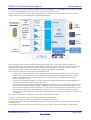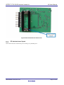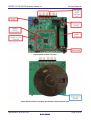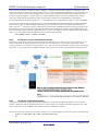
1
KIT USER MANUAL DETECT-IT ! RL78/I1D detector boards kit UM-YDETECT-IT-RL78 Rev.1.10 Jan 8, 2015 Kit User manual Introduction The Renesas kit Detect it! is based on the low power 16-bit microcontroller RL78/I1D. The kit contains 4 boards which are demonstrator of the most common detector types available in the market: - Glass break detector and motion detector used mainly in security & surveillance system Monoxide carbon detector and smoke detector used in human protection system. The user can easily test these 4 detector boards, indeed all the boards contained into the Detect it! kit are preprogrammed and ready for quick demonstration. The boards demonstrate the new Renesas microcontroller RL78/I1D specifically designed for detector applications, thanks to its low power features, enhanced analog front end and smart peripherals. The boards are designed to allow some flexibility. For example, nearly all pins of the microcontroller are connected to some header, the user can chose between power by line or power from a battery, the user can easily add a PMOD extension thanks to the 12 bit standard pin header sold onto the board. User can connect the boards to external tool for debugging and flashing the boards. Target Device RL78/I1D devices, Family part numbers starting with R5F117 UM-YDETECT-IT-RL78 V1.10 Page 1 of 57 DETECT-IT RL78/I1D detector boards kit Kit User Manual Contents 1. Hardware overview ......................................................................................................... 5 2. Detector application brief explanation .......................................................................... 5 Glass Break detector board design explanation ..................................................................... 5 CO detector design explanation ................................................................................................ 6 Motion detector design explanation ......................................................................................... 8 Smoke detector design explanation ......................................................................................... 9 3. Boards layout ............................................................................................................... 10 Glass Break detector board layout ......................................................................................... 10 CO detector board layout ......................................................................................................... 11 Motion detector board layout................................................................................................... 13 Smoke detector board layout................................................................................................... 14 4. Content of the CD-ROM ............................................................................................... 16 5. Board description ......................................................................................................... 16 Glass Break detector board ..................................................................................................... 16 5.1.1 Oscillators ............................................................................................................................. 18 5.1.2 Description of Jumper J ........................................................................................................ 18 5.1.3 Description of Potentiometer JP ........................................................................................... 18 5.1.4 Buzzer: .................................................................................................................................. 19 5.1.5 Description of Push Button ................................................................................................... 19 5.1.6 Battery place holder .............................................................................................................. 19 5.1.7 Microcontroller RL78/I1D ...................................................................................................... 19 5.1.8 Description of PMOD connector J9....................................................................................... 21 5.1.9 Description of board edge connectors CN01 and CN02 ...................................................... 21 CO detector board ..................................................................................................................... 22 5.2.1 Oscillators ............................................................................................................................. 23 5.2.2 Description of Jumper J ........................................................................................................ 23 5.2.3 Description of Potentiometer JP ........................................................................................... 24 5.2.4 Buzzer: .................................................................................................................................. 24 5.2.5 Description of Push Button ................................................................................................... 24 5.2.6 Battery place holder: ............................................................................................................. 25 5.2.7 Microcontroller RL78/I1D ...................................................................................................... 25 5.2.8 Description of PMOD connector J9....................................................................................... 27 5.2.9 Description of board edge connectors CN01 and CN02 ...................................................... 27 Motion detector board .............................................................................................................. 28 5.3.1 Oscillators ............................................................................................................................. 29 5.3.2 Description of Jumper J ........................................................................................................ 29 5.3.3 Description of Potentiometer JP ........................................................................................... 30 UM-YDETECT-IT-RL78 V1.10 Page 2 of 57 DETECT-IT RL78/I1D detector boards kit Kit User Manual 5.3.4 Buzzer ................................................................................................................................... 31 5.3.5 Description of Push Button ................................................................................................... 31 5.3.6 Battery place holder .............................................................................................................. 31 5.3.7 Microcontroller RL78/I1D ...................................................................................................... 31 5.3.8 Description of PMOD connector J9....................................................................................... 33 5.3.9 Description of board edge connectors CN01 and CN02 ...................................................... 33 Smoke detector board .............................................................................................................. 34 5.4.1 Sensor connection ................................................................................................................ 35 5.4.2 Oscillators ............................................................................................................................. 35 5.4.3 Description of Jumper J ........................................................................................................ 35 5.4.4 Description of Potentiometer JP ........................................................................................... 36 5.4.5 Buzzer ................................................................................................................................... 36 5.4.6 Description of Push Button ................................................................................................... 36 5.4.7 Battery place holder .............................................................................................................. 37 5.4.8 Microcontroller RL78/I1D ...................................................................................................... 37 5.4.9 Description of PMOD connector J9....................................................................................... 39 5.4.10 Description of board edge connectors CN01 and CN02 ...................................................... 39 6. Theory of operation ...................................................................................................... 40 Glass Break detector theory of operation .............................................................................. 40 6.1.1 Analog Front End circuit of Glass Break detector ................................................................. 40 6.1.2 MCU/digital system and maintain low current drain for long battery life ............................... 41 CO detector theory of operation .............................................................................................. 41 6.2.1 Analog Front End circuit of CO detector ............................................................................... 41 6.2.2 MCU/digital system and maintain low current drain for long battery life ............................... 42 Motion detector theory of operation ....................................................................................... 43 6.3.1 Analog Front End circuit of Motion Detector ......................................................................... 43 6.3.2 MCU/digital system and maintain low current drain for long battery life ............................... 44 Smoke detector theory of operation ....................................................................................... 44 6.4.1 Analog Front End circuit of Smoke detector ......................................................................... 44 6.4.2 MCU/digital system and maintain low current drain for long battery life ............................... 45 7. How to start the boards with IAR ................................................................................ 46 8. Notes and comments about board operation ............................................................. 50 Glass Break detector operation ............................................................................................... 50 8.1.1 Glass break Sensor Testing results ...................................................................................... 50 8.1.2 Glass break Sensor Current consumption results ................................................................ 50 CO Sensor Operation ................................................................................................................ 50 8.2.1 CO Sensor Testing results .................................................................................................... 50 8.2.2 CO Sensor Current Consumption results ............................................................................. 51 8.2.3 CO Sensor Calibration method ............................................................................................. 51 UM-YDETECT-IT-RL78 V1.10 Page 3 of 57 DETECT-IT RL78/I1D detector boards kit Kit User Manual Motion Detector Operation ....................................................................................................... 52 8.3.1 Motion Detector Testing results ............................................................................................ 52 8.3.2 Motion detector Current consumption results ....................................................................... 52 Smoke Sensor Operation ......................................................................................................... 53 9. 8.4.1 Smoke Detector Testing results ............................................................................................ 53 8.4.2 Smoke detector Current consumption results ....................................................................... 53 Support ......................................................................................................................... 54 Revision History .................................................................................................................... 1 General Precautions in the Handling of MPU/MCU Products ............................................. 2 UM-YDETECT-IT-RL78 V1.10 Page 4 of 57 DETECT-IT RL78/I1D detector boards kit 1. Kit User Manual Hardware overview The detector kit Detect it! is including 4 different types of detector demonstrator: - Glass Break detector demonstrator Monoxide Carbon detector demonstrator (also name CO detector) Motion detector demonstrator Smoke detector demonstrator The purpose of those boards is to show that the Renesas microcontroller RL78/I1D MCU - used in each board - is a perfect device for implementing low power sensor designs for detectors with a minimal of external components. In each case, the board show a different detection using the RL78/I1D and its embedded analog peripherals such as internal operational-amplifier, comparators and more optimized power saving MCU features. The new RL78/I1D has some major advantages for detection against previous RL78 MCU families. The Renesas MCU RL78/I1D has specific features that can benefit to such type of detectors/sensors, for example usually requiring low power features like low average current drain and long battery life. The RL78/I1D MCU has low power clock/timer and safety features in STOP mode that draw less than 1µA total, even when Real-Time-Counter operated with 32kHz crystal, Watchdog timer operated with 15kHz clock, 12-bit interval timer and Low Voltage Detect functions are all enabled, and all RAM data retained. The RL78/I1D also has integrated operational amplifiers and comparators that can be used for sensor measurements at low power. Current drain for the RL78/I1D integrated operational amplifiers and comparators depends on factors such as external bias resistor values, which operational amplifier and comparator modes are used and how many channels are enabled during standby. The integrated, internal RL78/I1D operational amplifiers have both a low power mode and high speed mode. In Low Power mode, the operational amplifier is typically drawing about 2.5µA typical for the first channel (plus ~2.0µA per each additional channel) with GainBandWidth (GBW) = 40kHz. In High Speed mode, the current draw is around 140µA typical for first channel (plus ~120µA per each additional channel) with GBW = 1.7MHz. All boards have a different sensor depending on the measurement that needs to be done: Glass Break detector demonstrator use a microphone to detect noise that emulate glass break event. Monoxide carbon detector (CO detector) demonstrator uses a chemical sensor Motion detector demonstrator use a specific PIR sensor based on infrared technology to detect movement. Smoke detector demonstrator use a smoke chamber, that can be replaced by emitter and receptor diode All boards are processing the measurement coming from these sensors with thanks to amplification and filtering stage done by the microcontroller. There is possibility to power each board by battery (3V lithium battery) or by power supply. All the detector boards demonstrate a low current consumption. For the purpose of the demonstration, the goal was to achieve a battery life of 4 years or more using a CR123 lithium battery. Further optimization can be done in true application to minimize further the current consumption of the board. 2. Detector application brief explanation Here are brief explanation of function of each board, including top level block diagram. Glass Break detector board design explanation The Glass Break detector is designed to start alarm when a glass break sound event occurred. By consequence the goal is to start alert when high frequency sound is detected, and the to filter all loud sounds such as loud hand clap, slamming door, book slammed down on a table or barking dog. It was designed to detect simulated glass break event, such as emulated by the Interlogix 5709C-W glass break simulator. UM-YDETECT-IT-RL78 V1.10 Page 5 of 57 DETECT-IT RL78/I1D detector boards kit Kit User Manual Figure Glass Break sensor block diagram The microphone is the first element of the analog front end. The microphone is used as the sensor for glass break event. The microphone used is an Electret condenser cartridge with frequency response from 25Hz to 16kHz. The microphone is AC coupled to both a low pass and high pass sections, so that microphone output DC bias variations does not affect the operational amplifier filter bias points: • 2-stage low pass filter uses 2 channels (Ch0 and Ch1) of RL78/I1D internal operational amplifiers in low power mode at about 4.5µA typical current drain total. The first stage has a nominal gain of 31 and a roll-off/cut-off frequency @ 34Hz. The second stage has a nominal gain of 26 at roll-off/cut-off frequency @ 154Hz. Therefore in both cases, GBWP (gain x frequency product) used on each stage is less that the operational amplifier GBW = 40 kHz rating in low power mode. Since the operational amplifiers have a low current drain in low power mode, they can be left on constantly to monitor a loud transient sound event. • 2-stage high pass filter uses 2 channels (Ch2 and Ch3) of RL78/I1D internal operational amplifiers in high speed mode at about 262µA total for both channels typical current drain. The first stage has a nominal gain of 20 and upper roll-off/cut-off frequency @ 24kHz. The second stage has a nominal gain of 5 and upper roll-off/cut-off frequency @ 1447Hz. Therefore in both cases, the GBWP (gain x frequency product) used is less that the operational amplifier GBW = 1.7 MHz rating in high speed mode. Since the operational amplifiers have a higher current drain (>100µA per channel) in high speed mode, they are only turned on intermittently when analyzing a loud sound transient event. So in glass break detector demonstration, the 4 operational amplifiers are used. A buzzer is used to give the alarm, it is managed by the MCU (transistor driver). The push button is used for the reset function. The board can be powered by a 3V lithium battery (CR123). It can also be powered by power supply (E1 power supply or external power). Caution: Battery should never be installed when using E1 power supply or external power supply via CN02/CN01. CO detector design explanation The monoxide carbon detector is designed to alarm when the concentration of CO gas is measured at a preset level of 100ppm. A higher threshold level can be set in software if desired. UM-YDETECT-IT-RL78 V1.10 Page 6 of 57 DETECT-IT RL78/I1D detector boards kit Kit User Manual The chemical sensor CO sensor canister is used to detect CO gas at 100ppm +/- 10 ppm and greater. An aerosol such as CO Check ™ or Model HO-CO rev2 test CO gas can be used to simulate an event. In the case of the CO detector, only 2 operational amplifiers are used: they are used to process CO sensor current to voltage and look for CO gas exceeding the pre-determined threshold. Figure CO sensor block diagram The CO chemical sensor is the first element of the analog front end. The CO gas sensor is used as the sensor for concentration of CO gas. It is a CO sensor canister (Figuro TGS5042 CO gas sensor) and it is used to provide a linear output current that is proportional with CO gas concentration. Its specification is 1.2nA-2.4nA per PPM, and the calibrated output value is printed on the canister (for example 1402 indicates 1.402nA/PPM) The CO sensor is connected to 2-stage processing analog front end: 1 stage DC bias: uses single channel (Ch1) of RL78/I1D internal operational amplifier in low power mode at about 2.25µA typical current drain. This stage implements a voltage follower configuration from a resistive divider at VDD/11 (nominally 0.3Volt @ VDD = 3.3V) and provides a low impedance to the CO sensor negative terminal bias point. 1 stage Trans-conductance amplifier: uses single channel (Ch0) of RL78/I1D internal operational amplifier in low power mode at about 2.25µA typical current drain. For the both the DC bias and Trans conductance amplifier configurations, the required frequency response is less than 1Hz and the operational amplifier GBW = 40kHz rating in low power mode is more than adequate. Since the 2 operational amplifier channels together have ~4.5µA typical current drain in low power mode, they can be left on without a huge increase in STOP/standby mode current. As the CO sensor has a relatively long time constant (>10 seconds) to fully react to the CO gas concentration levels, the operational amplifiers need to be left on constantly. So in this CO sensor detector demonstration, only 2 operational amplifiers are used. A buzzer is used to give the alarm, it is managed by the MCU (transistor driver). The push button is used connected, but not used in the CO detector demonstrator. The board can be powered by a 3V lithium battery (CR123). It can also be powered by power supply (E1 power supply or external power). Caution: Battery should never be installed when using E1 power supply or external power supply via CN02/CN01. UM-YDETECT-IT-RL78 V1.10 Page 7 of 57 DETECT-IT RL78/I1D detector boards kit Kit User Manual Motion detector design explanation The Motion detector demonstration can alarm when a human with mass of 50kg or greater moves within 4 meters in front of the PIR (Pyroelectric InfraRed) sensor within an angle of +/-45degrees vertically, and +/-70 degrees horizontally as measured from the normal (apex) point perpendicular to the front of PIR sensor surface. For this Motion sensor design, the 2 integrated operational amplifiers are used to monitor PIR sensor amplified voltage and look for PIR levels exceeding the pre-determined thresholds. The operational amplifiers are used in high speed mode in this Motion sensor demonstrator. Figure Motion sensor block diagram: The PIR (Pyroelecctric InfraRed) sensor is the first element of the Analog Front End. The muRata part number IRAE700STO PIR sensor is used to detect IR energy changes that are detected when a warm object such as a human being comes into the range of the sensor. PIR sensing of infrared energy is further enhanced by a white, translucent Fresnel lens placed in front of the PIR transducer. The Fresnel lens has a hemispheric shape with a honey comb shaped cells in the plastic mold. These Fresnel lens cell shapes then enhance the sensed IR energy peak-to-peak voltage changes as the human being advances across the front of PIR sensor The PIR sensor is connected to 2-stage processing analog front end: The first stage AC amplifier uses single channel Ch1 of RL78/I1D internal operational-amplifier in low power mode at about 2.25µA typical current drain. This stage is AC coupled from the PIR sensor output to Ch1, so as to eliminate any PIR DC bias variations. The stage 1 amplifier has a nominal gain of x101, and an upper roll-off frequency ~15.9Hz. The second stage AC amplifier: uses single op-amp channel Ch0 has a nominal gain of x33.9 max (x6.7min) at roll-off/cut-off frequency @32.9HZ max (6.5HZ min). The gain of this 2nd stage is adjust by the 900KΩ potentiometer (labeled JP9). The input of the 2nd stage is AC coupled (DC-blocked) from 1st stage (AMP1O) output. However the output of 2nd stage (AMP0O) is DC coupled to ADC input ANI4 and Comparator input IVREF0. In all cases of the 1st stage and 2nd stage Amplifier settings, GBWP (gain x frequency product) used on each stage is less that the op-amp GBW = 40KHZ rating in low power mode. Since the op-amps have a low current drain in low power mode, they can be left on constantly to monitor PIR sensor pulse energy. The output of AMP0O is monitored by Comparator input IVCMP0, which is on the same MCU pin as AMP0O. The explanation of Comparator function to trigger MCU wakeup is below. So in this Motion sensor detector demonstration, only 2 operational amplifiers are used. UM-YDETECT-IT-RL78 V1.10 Page 8 of 57 DETECT-IT RL78/I1D detector boards kit Kit User Manual Note : The motion sensor board has a second/alternate PIR sensor connected to MCU internal operational amplifier channels Ch2 and Ch3. However, these Ch2/Ch3 operational amplifiers are not currently activated by the current Firmware revision, and as long as jumpers are not populated on header J8, then the second PIR sensor will not draw current. (However there is an additional current drain thru R67 and R93 of about 0.34uA @3.3V that could be eliminated by removing either of these resistors). A buzzer is used to give the alarm, it is managed by the MCU (transistor driver). The push button is used for the reset function. The board can be powered by a 3V lithium battery (CR123). It can also be powered by power supply (E1 power supply or external power). Caution: Battery should never be installed when using E1 power supply or external power supply via CN02/CN01. Smoke detector design explanation The Smoke detector is an infrared reflective smoke sensor type. It will alert when smoke (or simulated smoke) is detected for 3 seconds. In order to test the smoke detector board, you can use product like “smoke check” or “smoke in a can” brand spray in order to simulated smoke. The board will work with real smoke as well. The board is designed to reject any ambient infrared light from direct/indirect sunlight or man-made IR sources. For the smoke sensor, the integrated operational amplifiers of the RL78/I1D are used to perform the current to voltage (trans-conductance) conversion needed to detect IR photodiode avalanche (reverse bias) current when reflected IR light is present. Only 2 operational amplifiers are used in the Smoke detector demonstrator, and they are operating in High Speed mode. The RL78/I1D comparators are not used for this Smoke detector design. Figure Smoke sensor block diagram The optical smoke chamber is the first element of the analog front end, this chamber is used to reduce the ambient light. Inside an Infrared emitting LED and Infrared Photodiode are used to detect smoke particles by reflected IR light. This optical smoke chamber is connected to 2 operational amplifiers of the RL78/I1D : First stage (DC) trans-conductance (current to voltage) amplifier Second stage DC amplifier, to provided additional DC gain. The on-chip comparators are not used in the Smoke sensor board. A buzzer is used to give the alarm, it is managed by the MCU (transistor driver). The push button is used for the reset function. UM-YDETECT-IT-RL78 V1.10 Page 9 of 57 DETECT-IT RL78/I1D detector boards kit Kit User Manual The board can be powered by a 3V lithium battery (CR123). It can also be powered by power supply (E1 power supply or external power). Caution: Battery should never be installed when using E1 power supply or external power supply via CN02/CN01. 3. Boards layout Here are a picture of the all the boards with short explanation of the main parts. The name of each board is written, on the PCB (Please look at the PCB to identify each board). Glass Break detector board layout Please check the name of the board you are looking “GLASSBREAK_SENSOR_I1D” Figure Glass break detector top view UM-YDETECT-IT-RL78 V1.10 Page 10 of 57 DETECT-IT RL78/I1D detector boards kit Kit User Manual Figure Glass break detector bottom view CO detector board layout Please check the name of the board you are looking “CO_SENSOR_I1D” UM-YDETECT-IT-RL78 V1.10 Page 11 of 57 DETECT-IT RL78/I1D detector boards kit Kit User Manual Figure CO detector top view UM-YDETECT-IT-RL78 V1.10 Page 12 of 57 DETECT-IT RL78/I1D detector boards kit Kit User Manual Figure CO detector bottom view Motion detector board layout Please check the name of the board you are looking “MOTION_SENSOR_I1D” Figure Motion detector top view UM-YDETECT-IT-RL78 V1.10 Page 13 of 57 DETECT-IT RL78/I1D detector boards kit Kit User Manual Figure Motion detector bottom view Smoke detector board layout Please check the name of the board you are looking “SMOKE_SENSOR_I1D” UM-YDETECT-IT-RL78 V1.10 Page 14 of 57 DETECT-IT RL78/I1D detector boards kit Kit User Manual Figure Smoke detector top view Figure Smoke detector equipped with Smoke chamber bottom view UM-YDETECT-IT-RL78 V1.10 Page 15 of 57 DETECT-IT RL78/I1D detector boards kit Kit User Manual Figure Smoke detector equipped with IR emitter and receiver bottom view 4. Content of the CD-ROM The CD content is listed here: Table CD ROM content list CD ROM folder User Manual Embedded software Documentation 5. Description of resources • User manual of the kit • User manual of the device RL78/I1D • Quick start guide of the kit IAR Samples programs for each demonstrators boards • IAR samples program for Glass Break demonstrator • IAR samples program for CO demonstrator • IAR samples program for Motion demonstrator • IAR samples program for Smoke demonstrator For each demonstrator boards : • Schematics • Gerber files • Bill of Material Board description Glass Break detector board UM-YDETECT-IT-RL78 V1.10 Page 16 of 57 DETECT-IT RL78/I1D detector boards kit Kit User Manual Figure Glass Break detector components top view UM-YDETECT-IT-RL78 V1.10 Page 17 of 57 DETECT-IT RL78/I1D detector boards kit Kit User Manual Figure Glass Break detector components bottom view 5.1.1 Oscillators Each board is equipped with 2 oscillators: • A 20MHz oscillator The 20MHz oscillator is sold onto each board and connected to the MCU. But it is not used by the application. Instead the internal High Speed on-chip oscillator of the RL7/I1D is used by each application. So pin P121/X1 and pin P122/X2 are used as Input. • Please change the settings if you wish to use the external oscillator. • A 32,768kHz quartz It is connected to the MCU It is operating and used by the application (especially by the RTC). 5.1.2 Table Jumper J1 Description of Jumper J Description of jumper of Glass Break detector Status Closed Open J2 Closed Open J3 Closed Open Function Power supply of the MCU and others components [MCU, Alarm/buzzer, AVDD via L1, U1 Vin (optional), pull up resistors, R16/R10 and R13/R19]: power from battery or power from E1 via CN01-pin 5, CN02-pin 4 Caution: Battery should never be installed when using E1 power supply or external power supply via CN02/CN01 Current measurement of the MCU and others components [MCU, Alarm/buzzer, L1and AVDD, U2 Vin (optional), pull up resistors] by connection of the ampere meter Power supply of some components [R18, R17, R15, R11, J3] on glass break detectors board Current measurement of some components [R18, R17, R15, R11, J3] by connection of the ampere meter Usage of RL78/I1D comparators (motion detector and glass break detector board) Comparators are not used, IVREF0 & IVREF1 are not used (CO detector and smoke detector board) In order to start the demonstration of the Glass Break detector, please ensure that this initial configuration is done: • J1 should be closed • J2 should be closed • J3 should be closed 5.1.3 Table Description of Potentiometer JP Description of potentiometer of Glass Break detector UM-YDETECT-IT-RL78 V1.10 Page 18 of 57 DETECT-IT RL78/I1D detector boards kit Potentiometer JP10 Function IVREF1 comparator 1 JP11 IVREF0 comparator 0 5.1.4 Kit User Manual Comment Set JP10 potentiometer for IVREF1 (DNI_J3, pin 1) = 2.0V Approximately (0.58*VDD) at VDD = 3.4V (Use a voltmeter with at least 10MΩ input impedance as lower impedance (such as 1MΩ) will significantly load down the resistor bias chain). Set JP11 potentiometer for IVREF0 (DNI_J2, Pin 12) = 1.2V Approximately. (0.35*VDD) at VDD = 3.4V (Use a voltmeter with at least 10MΩ input impedance as lower impedance (such as 1MΩ) will significantly load down the resistor bias chain). Buzzer: The buzzer is used for alarm by the application. It is connected to MCU pin P01/PCLBUZ1 5.1.5 Description of Push Button The push button is connected MCU pin P137 / INTP0 via R3, and used as “Reset” function. The Interrupt function can be found in the project file “r_cg_intc_user.c” Table Description of push button of Glass Break detector Button Status Function SW1 Un-pressed Pressed INTP0 is high – no operation INTP0 goes low – interrupt function is executed which defeats alarm (software depending) 5.1.6 Battery place holder Each board is equipped with a CR123 battery holder. There is a reverse polarity protection (P-channel MOSFET). Be careful when placing the battery to pay attention to the polarity. Caution: Battery should never be installed when using E1 power supply or external power supply via CN02/CN01. 5.1.7 Microcontroller RL78/I1D The Renesas 48-pin RL78/I1D MCU is the main element of the demonstrator board. The reference used in this demonstrator is the biggest component of the family RL78/I1D. It is a 48 pin QFP package with 32kB Flash and 3kB RAM embedded. The part number is: R5F117GCGFB. The 48-pin RL78/I1D MCU has 4 channels of operational amplifier, 2 channels of comparators, and a total of 41 I/O lines (including digital and analog interfaces). 4 headers of 12-pin each that bring out most of the MCU I/O pins. Pins for access to device port: all pins of the RL78/I1D MCU are connected to: UM-YDETECT-IT-RL78 V1.10 Page 19 of 57 DETECT-IT RL78/I1D detector boards kit Kit User Manual Connector Pin RL78/I1D port name Function DNI_J1 1 2 3 4 5 6 7 8 9 10 11 12 1 2 3 4 5 6 7 8 9 10 11 12 1 2 3 4 5 6 7 8 9 10 11 12 1 2 3 4 5 6 7 8 9 10 11 12 P01/PCLBUZ1 P00 /RESET P124/XT2/EXCLKS P132/XT1 P137/INTP0 P122/X2/EXCLK P121/X1 REGC VSS VDD P60 P61 P62 P63/SSI00 P57/(TI03/TO03)/INTP4/VCOUT1 P56/SCK00/SCL00/INTP3 P55/SI00/RxD0/SDA00/INTP2/TOOLRXD P54/SO00/TxD0/INTP1/TOOLTXD P53/KR2/SO01/VCOUT0 P52/KR1/SI01/SDA01/TI03/TO03 P51/KR0/SCK01/SCL01/TI02/TO02 P50/(TI00/TO01)/RTC1HZ P30/(SCK00)/(SCL00)/TI00/TO01/IVREF0 P31/TI01/TO00/PCLBUZ0/IVREF1 P32/KR3/(TI01/TO00)/INTP6 P33/(TI02/TO02)/INTP5 P20/ANI13/IVCMP1/AMP3O P21/ANI12/AMP3P22/ANI11/AMP3+ P23/ANI10/AMP2O P24/ANI9/AMP2P25/ANI8/AMP2+ AVDD AVSS P17/ANI7/AMP1O P16/ANI6/AMP1P15/ANI5/AMP1+ P14/ANI4/IVCMP0/AMP0O P13/ANI3/AMP0P12/ANI2/AMP0+ P11/ANI1/AVREFM P10/ANI0/AVREFP P130 P40/TOOL0 P04/ANI18 P03/ANI17 P02/ANI16 BUZZER P00 RESET XT1 XT2 SW1 input P122 P121 REGC VSS VDD P60 DNI_J2 DNI_J3 DNI_J4 UM-YDETECT-IT-RL78 V1.10 OUT2 OUT1 IVREF0 IVREF1 P32 P33 AMP3O AMP3AMP3+ AMP2O AMP2AMP2+ AVDD AVSS AMP1O AMP1AMP1+ AMP0O AMP0AMP0+ Page 20 of 57 DETECT-IT RL78/I1D detector boards kit 5.1.8 Kit User Manual Description of PMOD connector J9 It is a 12-pin (2x6) SPI PMOD standard interface: It can be used to add external application boards such as WiFi/wireless. Table Description of PMOD connector of Glass Break detector Connector Pin Function J9 1 2 3 4 5 6 7 8 9 10 11 12 MCU P63 MCU P57 MCU P54 MCU P32 MCU P55 MCU P52 MCU P56 MCU P33 GND GND VDD VDD 5.1.9 Description of board edge connectors CN01 and CN02 There are a 14/26 dual row edge connector that has dual use of: • E1 on-chip debug/flash connection : This interface can be used with for debug session or for flash programming session. E1 on-chip emulator and flash programmer 14-pin ribbon cable is connected to CN01 (pins 1-7) and CN02 (pins 17) for debug and flash programming. Pin 1 of E1 ribbon cable is oriented to CN01-pin 1. However, reverse connection between E1 and CN01/CN02 pins 1-7 will not cause board damage. • 26-pin TK-interface board. Table Description of board edge connector of Glass Break detector Connector CN01 Pin # 1 2 3 Function No Connect (E1) No Connect (E1) Tool0 (E1) E1 pin # 1 3 5 4 5 6 7 8 9 10 11 12 13 No Connect (E1) VDD (E1) No Connect (E1) RESET (E1) No pin MCU P63 MCU P54 MCU P55 MCU P56 No Connect 7 9 11 13 ` ` ` ` ` ` UM-YDETECT-IT-RL78 V1.10 Connector CN02 Pin # 1 2 3 4 5 6 7 8 9 10 11 12 13 Function GND (E1) No Connect (E1) T_RESET (RESET IN) (E1) VDD (E1) RESET (E1) GND (E1) GND (E1) No pin No Connect No Connect No Connect No Connect No Connect E1 pin # 2 4 6 8 10 12 14 ` ` ` ` ` ` Page 21 of 57 DETECT-IT RL78/I1D detector boards kit Kit User Manual CO detector board Figure CO detector components top view UM-YDETECT-IT-RL78 V1.10 Page 22 of 57 DETECT-IT RL78/I1D detector boards kit Kit User Manual Figure CO detector components bottom view 5.2.1 Oscillators Each board is equipped with 2 oscillators: • A 20 MHz oscillator The 20 MHz oscillator is sold onto each board and connected to the MCU. But it is not used by the application. Instead the internal High Speed on-chip oscillator of the RL7/I1D is used by each application. So pin P121/X1 and pin P122/X2 are used as Input. • Please change the settings if you wish to use the external oscillator. • A 32,768kHz quartz It is connected to the MCU It is operating and used by the application (especially by the RTC). 5.2.2 Table Description of Jumper J Description of jumper of CO detector UM-YDETECT-IT-RL78 V1.10 Page 23 of 57 DETECT-IT RL78/I1D detector boards kit Jumper J1 Status Closed Open J2 Closed Open J4 DN_J10 Opened 1-2 2-3 Closed Open DN_J14 Closed Open Kit User Manual Function Power supply of the MCU and others components [MCU, Alarm/buzzer, AVDD via L1, U1 Vin (optional), pull up resistors, R16/R10 and R13/R19]: power from battery or power from E1 via CN01-pin 5, CN02-pin 4 Caution : Battery should never be installed when using E1 power supply or external power supply via CN02/CN01 Current measurement of the MCU and others components [MCU, Alarm/buzzer, L1and AVDD, U2 Vin (optional), pull up resistors] by connection of the ampere meter Power supply of some components [R18, R17, R15, R11, J3] on glass break detectors board Current measurement of some components [R18, R17, R15, R11, J3] by connection of the ampere meter Normal operation Optional REGC = 1.8V to AVREFP (with SW change) Optional AIC1702L-25 output = 2.5V to AVREFP (with SW change) Use less – no amplification of trans impedance amplifier May bypass with Resistor to change the Impedance Filter (R45 & C20 used) between Amp0 Out and Amp0 – Direct connection to Ground (please check schematics for more details) - no influence for the CO detector application R32 is used (please check schematics for more details) - no influence for the CO detector application In order to start the demonstration of the CO detector, please ensure that this initial configuration is done: • • • • J1 should be closed J2 should be closed DN_J10 should be open DN_J14 can be closed or opened 5.2.3 Table Description of Potentiometer JP Description of potentiometer of CO detector Potentiometer JP10 JP11 5.2.4 Status IVREF1 comparator 1 IVREF0 comparator 0 Function Could be used when J3 is closed (please check schematics for more details). Could be used when J3 is closed (please check schematics for more details). Buzzer: The buzzer is used for alarm by the application. It is connected to MCU pin P01/PCLBUZ1 5.2.5 Description of Push Button The push button is connected MCU pin P137 / INTP0 via R3. It is not used in the current CO detector application. Table Description of push button of CO detector Button Status Function SW1 Un-pressed Pressed INTP0 is High – no operation INTP0 goes Low – no operation UM-YDETECT-IT-RL78 V1.10 Page 24 of 57 DETECT-IT RL78/I1D detector boards kit 5.2.6 Kit User Manual Battery place holder: Each board is equipped with a CR123 battery holder. There is a reverse polarity protection (P-channel MOSFET). Be careful when placing the battery to pay attention to the polarity. Caution: Battery should never be installed when using E1 power supply or external power supply via CN02/CN01 5.2.7 Microcontroller RL78/I1D The Renesas 48-pin RL78/I1D MCU is the main element of the demonstrator board. The reference used in this demonstrator is the biggest component of the family RL78/I1D. It is a 48 pin QFP package with 32kB Flash and 3kB RAM embedded. The part number is: R5F117GCGFB. The 48-pin RL78/I1D MCU has 4 channels of operational amplifier, 2 channels of comparators, and a total of 41 I/O lines (including digital and analog interfaces) 4 headers of 12-pin each that bring out most of the MCU I/O pins. Pins for access to device port: all pins of the RL78/I1D MCU are connected to: Table Description of connector of CO detector UM-YDETECT-IT-RL78 V1.10 Page 25 of 57 DETECT-IT RL78/I1D detector boards kit Kit User Manual Connector Pin RL78/I1D port name Function DNI_J1 1 2 3 4 5 6 7 8 9 10 11 12 1 2 3 4 5 6 7 8 9 10 11 12 1 2 3 4 5 6 7 8 9 10 11 12 1 2 3 4 5 6 7 8 9 10 11 12 P01/PCLBUZ1 P00 /RESET P124/XT2/EXCLKS P132/XT1 P137/INTP0 P122/X2/EXCLK P121/X1 REGC VSS VDD P60 P61 P62 P63/SSI00 P57/(TI03/TO03)/INTP4/VCOUT1 P56/SCK00/SCL00/INTP3 P55/SI00/RxD0/SDA00/INTP2/TOOLRXD P54/SO00/TxD0/INTP1/TOOLTXD P53/KR2/SO01/VCOUT0 P52/KR1/SI01/SDA01/TI03/TO03 P51/KR0/SCK01/SCL01/TI02/TO02 P50/(TI00/TO01)/RTC1HZ P30/(SCK00)/(SCL00)/TI00/TO01/IVREF0 P31/TI01/TO00/PCLBUZ0/IVREF1 P32/KR3/(TI01/TO00)/INTP6 P33/(TI02/TO02)/INTP5 P20/ANI13/IVCMP1/AMP3O P21/ANI12/AMP3P22/ANI11/AMP3+ P23/ANI10/AMP2O P24/ANI9/AMP2P25/ANI8/AMP2+ AVDD AVSS P17/ANI7/AMP1O P16/ANI6/AMP1P15/ANI5/AMP1+ P14/ANI4/IVCMP0/AMP0O P13/ANI3/AMP0P12/ANI2/AMP0+ P11/ANI1/AVREFM P10/ANI0/AVREFP P130 P40/TOOL0 P04/ANI18 P03/ANI17 P02/ANI16 BUZZER P00 RESET XT1 XT2 SW1 input P122 P121 REGC VSS VDD P60 DNI_J2 DNI_J3 DNI_J4 UM-YDETECT-IT-RL78 V1.10 OUT2 OUT1 IVREF0 IVREF1 P32 P33 AMP3O AMP3AMP3+ AMP2O AMP2AMP2+ AVDD AVSS AMP1O AMP1AMP1+ AMP0O AMP0AMP0+ Page 26 of 57 DETECT-IT RL78/I1D detector boards kit 5.2.8 Kit User Manual Description of PMOD connector J9 It is a 12-pin (2x6) SPI PMOD standard interface: It can be used to add external application boards such as WiFi/wireless Table Description of PMOD of CO detector Connector Pin Function J9 1 2 3 4 5 6 7 8 9 10 11 12 MCU P63 MCU P57 MCU P54 MCU P32 MCU P55 MCU P52 MCU P56 MCU P33 GND GND VDD VDD 5.2.9 Description of board edge connectors CN01 and CN02 There are a 14/26 dual row edge connector that has dual use of: • E1 on-chip debug/flash connection : This interface can be used with for debug session or for flash programming session. E1 on-chip emulator and flash programmer 14-pin ribbon cable is connected to CN01 (pins 1-7) and CN02 (pins 17) for debug and flash programming. Pin 1 of E1 ribbon cable is oriented to CN01-pin 1. However, reverse connection between E1 and CN01/CN02 pins 1-7 will not cause board damage. • 26-pin TK-interface board. Table Description of edge connector of CO detector Connector CN01 Pin # 1 2 3 Function No Connect (E1) No Connect (E1) Tool0 (E1) E1 pin # 1 3 5 4 5 6 7 8 9 10 11 12 13 No Connect (E1) VDD (E1) No Connect (E1) RESET (E1) No pin MCU P63 MCU P54 MCU P55 MCU P56 No Connect 7 9 11 13 ` ` ` ` ` ` UM-YDETECT-IT-RL78 V1.10 Connector CN02 Pin # 1 2 3 4 5 6 7 8 9 10 11 12 13 Function GND (E1) No Connect (E1) T_RESET (RESET IN) (E1) VDD (E1) RESET (E1) GND (E1) GND (E1) No pin No Connect No Connect No Connect No Connect No Connect E1 pin # 2 4 6 8 10 12 14 ` ` ` ` ` ` Page 27 of 57 DETECT-IT RL78/I1D detector boards kit Kit User Manual Motion detector board Here are the pictures of the motion sensor board Figure Motion detector components top view UM-YDETECT-IT-RL78 V1.10 Page 28 of 57 DETECT-IT RL78/I1D detector boards kit Kit User Manual Figure Motion detector components bottom view 5.3.1 Oscillators Each board is equipped with 2 oscillators: • A 20 MHz oscillator The 20 MHz oscillator is sold onto each board and connected to the MCU. But it is not used by the application. Instead the internal High Speed on-chip oscillator of the RL7/I1D is used by each application. So pin P121/X1 and pin P122/X2 are used as Input. • Please change the settings if you wish to use the external oscillator. • A 32,768kHz quartz It is connected to the MCU It is operating and used by the application (especially by the RTC). 5.3.2 Table Description of Jumper J Description of jumper of Motion detector UM-YDETECT-IT-RL78 V1.10 Page 29 of 57 DETECT-IT RL78/I1D detector boards kit Jumper J1 Status Closed Open J2 Closed Open J3 Closed Open J8 Open 1-2 2-3 Kit User Manual Function Power supply of the MCU and others components [MCU, Alarm/buzzer, L1and AVDD, U1 Vin (optional), pull up resistors]: power from battery or power from E1 via CN01-pin 5, CN02-pin 4 Caution : Battery should never be installed when using E1 power supply or external power supply via CN02/CN01 Current measurement of the MCU and others components [MCU, Alarm/buzzer, L1and AVDD, U2 Vin (optional), pull up resistors] by connection of the ampere meter Power supply of some components [R87, R95, R64/R88, R67/R93, J3] on motion detector board Current measurement of some components [R87, R95, R64/R88, R67/R93, J3] by connection of the ampere meter Usage of RL78/I1D comparators (motion detector and glass break detector board) Comparators are not used, IVREF0 & IVREF1 are not used (CO detector and smoke detector board) Single PIR sensor operation (Second PIR sensor is not powered) Dual PIR sensor operation with single bias - second PIR is powered with same power supply as first PIR sensor, via the same resistor R87. (Some software change is necessary to use dual PIR operation with single bias) Dual PIR sensor operation with separate bias (with SW change) - second PIR is powered with independent power supply. (Some software change is necessary to use dual PIR operation with separate bias) In order to start the demonstration of the Motion detector, please ensure that this initial configuration is done: • • • • J1 should be closed J2 should be closed J3 should be closed J8 should be opened 5.3.3 Table Description of Potentiometer JP Description of potentiometer of Motion detector UM-YDETECT-IT-RL78 V1.10 Page 30 of 57 DETECT-IT RL78/I1D detector boards kit Potentiometer JP9 Status Used to set the 2nd operation amplifier Gain (for Sensor 1) JP10 Used to set up IVREF1 JP11 Used to set up IVREF0 JP12 Used to set the 2nd operation amplifier Gain (for Sensor 2) 5.3.4 Kit User Manual Function Set JP9 pot for about 50% (mid-point) of rotation, and CW rotation of JP9 increases motion sensitivity. The Motion sensor can be empirically tested to alarm starting at 4-5 meter distance by rotating JP9 pot clockwise to increase sensitivity. However, too much sensitivity may cause some false alarms due to ambient IR light sources (incident outside light, etc). Set JP10 pot for IVREF1 (DNI_J3, pin 1) = 2.1V Approximately (0.62*VDD) at VDD = 3.4V (Use a voltmeter with at least 10MΩ input impedance as lower impedance (such as 1Meg) will significantly load down the resistor bias chain). Set JP11 pot for IVREF0 (DNI_J2, Pin 12) = 0.85V Approximately (0.25*VDD) at VDD = 3.4V (Use a voltmeter with at least 10MΩ input impedance as lower impedance (such as 1Meg) will significantly load down the resistor bias chain). Same function as JP9, but for Sensor 2 (beside C25) Buzzer The buzzer is used for alarm by the application. It is connected to MCU pin P01/PCLBUZ1. 5.3.5 Description of Push Button The push button is connected MCU pin P137 / INTP0 via R3, and used as “Reset” function. The Interrupt function can be found in the project file “r_cg_intc_user.c” Table Description of push button of Motion detector Button Status Function SW1 Un-pressed Pressed INTP0 is high – no operation INTP0 goes low – interrupt function is executed which defeats alarm (software depending) 5.3.6 Battery place holder Each board is equipped with a CR123 battery holder. There is a reverse polarity protection (P-channel MOSFET). Be careful when placing the battery to pay attention to the polarity. Caution: Battery should never be installed when using E1 power supply or external power supply via CN02/CN01. 5.3.7 Microcontroller RL78/I1D The Renesas 48-pin RL78/I1D MCU is the main element of the demonstrator board. The reference used in this demonstrator is the biggest component of the family RL78/I1D. It is a 48 pin QFP package with 32kB Flash and 3kB RAM embedded. The part number is: R5F117GCGFB. The 48-pin RL78/I1D MCU has 4 channels of operational amplifier, 2 channels of comparators, and a total of 41 I/O lines (including digital and analog interfaces). 4 headers of 12-pin each that bring out most of the MCU I/O pins. Pins for access to device port: all pins of the RL78/I1D MCU are connected to: Table Description of connector of Motion detector UM-YDETECT-IT-RL78 V1.10 Page 31 of 57 DETECT-IT RL78/I1D detector boards kit Kit User Manual Connector Pin RL78/I1D port name Function DNI_J1 1 2 3 4 5 6 7 8 9 10 11 12 1 2 3 4 5 6 7 8 9 10 11 12 1 2 3 4 5 6 7 8 9 10 11 12 1 2 3 4 5 6 7 8 9 10 11 12 P01/PCLBUZ1 P00 /RESET P124/XT2/EXCLKS P132/XT1 P137/INTP0 P122/X2/EXCLK P121/X1 REGC VSS VDD P60 P61 P62 P63/SSI00 P57/(TI03/TO03)/INTP4/VCOUT1 P56/SCK00/SCL00/INTP3 P55/SI00/RxD0/SDA00/INTP2/TOOLRXD P54/SO00/TxD0/INTP1/TOOLTXD P53/KR2/SO01/VCOUT0 P52/KR1/SI01/SDA01/TI03/TO03 P51/KR0/SCK01/SCL01/TI02/TO02 P50/(TI00/TO01)/RTC1HZ P30/(SCK00)/(SCL00)/TI00/TO01/IVREF0 P31/TI01/TO00/PCLBUZ0/IVREF1 P32/KR3/(TI01/TO00)/INTP6 P33/(TI02/TO02)/INTP5 P20/ANI13/IVCMP1/AMP3O P21/ANI12/AMP3P22/ANI11/AMP3+ P23/ANI10/AMP2O P24/ANI9/AMP2P25/ANI8/AMP2+ AVDD AVSS P17/ANI7/AMP1O P16/ANI6/AMP1P15/ANI5/AMP1+ P14/ANI4/IVCMP0/AMP0O P13/ANI3/AMP0P12/ANI2/AMP0+ P11/ANI1/AVREFM P10/ANI0/AVREFP P130 P40/TOOL0 P04/ANI18 P03/ANI17 P02/ANI16 BUZZER P00 RESET XT1 XT2 SW1 input P122 P121 REGC VSS VDD P60 DNI_J2 DNI_J3 DNI_J4 UM-YDETECT-IT-RL78 V1.10 OUT2 OUT1 IVREF0 IVREF1 P32 P33 AMP3O AMP3AMP3+ AMP2O AMP2AMP2+ AVDD AVSS AMP1O AMP1AMP1+ AMP0O AMP0AMP0+ Page 32 of 57 DETECT-IT RL78/I1D detector boards kit 5.3.8 Kit User Manual Description of PMOD connector J9 It is a 12-pin (2x6) SPI PMOD standard interface: It can be used to add external application boards such as WiFi/wireless Table Description of PMOD of Motion detector Connector Pin Function J9 1 2 3 4 5 6 7 8 9 10 11 12 MCU P63 MCU P57 MCU P54 MCU P32 MCU P55 MCU P52 MCU P56 MCU P33 GND GND VDD VDD 5.3.9 Description of board edge connectors CN01 and CN02 There are a 14/26 dual row edge connector that has dual use of: • E1 on-chip debug/flash connection : This interface can be used with for debug session or for flash programming session. E1 on-chip emulator and flash programmer 14-pin ribbon cable is connected to CN01 (pins 1-7) and CN02 (pins 17) for debug and flash programming. Pin 1 of E1 ribbon cable is oriented to CN01-pin 1. However, reverse connection between E1 and CN01/CN02 pins 1-7 will not cause board damage. • 26-pin TK-interface board. Table Description of edge connector of Motion detector Connector CN01 Pin # 1 2 3 Function No Connect (E1) No Connect (E1) Tool0 (E1) E1 pin # 1 3 5 4 5 6 7 8 9 10 11 12 13 No Connect (E1) VDD (E1) No Connect (E1) RESET (E1) No pin MCU P63 MCU P54 MCU P55 MCU P56 No Connect 7 9 11 13 ` ` ` ` ` ` UM-YDETECT-IT-RL78 V1.10 Connector CN02 Pin # 1 2 3 4 5 6 7 8 9 10 11 12 13 Function GND (E1) No Connect (E1) T_RESET (RESET IN) (E1) VDD (E1) RESET (E1) GND (E1) GND (E1) No pin No Connect No Connect No Connect No Connect No Connect E1 pin # 2 4 6 8 10 12 14 ` ` ` ` ` ` Page 33 of 57 DETECT-IT RL78/I1D detector boards kit Kit User Manual Smoke detector board Here are the pictures of the smoke sensor board: Figure Smoke detector components top view UM-YDETECT-IT-RL78 V1.10 Page 34 of 57 DETECT-IT RL78/I1D detector boards kit Kit User Manual Figure Smoke detector components bottom view 5.4.1 Sensor connection Please be careful when connecting the IR LED and IR photodiode. Table Description of sensor connector of Smoke detector Sensor IR photodiode IR LED 5.4.2 Connector & pins J10 – pins 7 & 8 receive J11 – pins 1 & 2 transmit Function Connection of IR photodiode : Cathode K on pin 8 (J10-pin8), Anode A on pin 7 (J10-pin7) Connection of IR LED : Cathode K on pin 1 (J11-pin 1), Anode A on pin 2 (J11-pin 2) Oscillators Each board is equipped with 2 oscillators: • A 20 MHz oscillator The 20 MHz oscillator is sold onto each board and connected to the MCU. But it is not used by the application. Instead the internal High Speed on-chip oscillator of the RL7/I1D is used by each application. So pin P121/X1 and pin P122/X2 are used as Input. • Please change the settings if you wish to use the external oscillator. • A 32,768kHz quartz It is connected to the MCU It is operating and used by the application (especially by the RTC). 5.4.3 Table Description of Jumper J Description of jumper of Smoke detector UM-YDETECT-IT-RL78 V1.10 Page 35 of 57 DETECT-IT RL78/I1D detector boards kit Jumper J1 Status Closed Open J2 Closed Open J3 Closed Open J6 J7 Closed Opened Closed 1-2 Closed 2-3 Kit User Manual Function Power supply of the MCU and others components [MCU, Alarm/buzzer, AVDD via L1, U1 Vin (optional), pull up resistors]: power from battery or power from E1 via CN01-pin 5, CN02-pin 4 Caution: Battery should never be installed when using E1 power supply or external power supply via CN02/CN01 Current measurement of the MCU and others components [MCU, Alarm/buzzer, L1and AVDD, U2 Vin (optional), pull up resistors] by connection of the ampere meter Power supply of some components [R67/68, J6] on motion detector board Current measurement of some components [R67/R68, J6] by connection of the ampere meter Usage of Rl78/I1D comparators (motion detector and glass break detector board) Comparators are not used, IVREF0 & IVREF1 are not used (CO detector and smoke detector board) Enable IR LED transmission (Provide CON2/J11 with VDD_Sensor) Disable IR LED transmission. Enable IR LED photodiode reception (Normal Operation) Disable IR LED photodiode transmission, could be used by test mode (with SW change) In order to start the demonstration of the Smoke detector, please ensure that this initial configuration is done: • J1 should be closed • J2 should be closed • J3 should be open • J6 should be closed • J7 (pins 1-2) should be closed • Connect IR LED and IR photodiode as show in the table above. 5.4.4 Table Description of Potentiometer JP Description of potentiometer of Smoke detector Potentiometer JP10 JP11 5.4.5 Status IVREF1 comparator 1 IVREF0 comparator 0 Function Could be used when J3 is closed (please check schematics for more details). Could be used when J3 is closed (please check schematics for more details). Buzzer The buzzer is used for alarm by the application. It is connected to MCU pin P01/PCLBUZ1 5.4.6 Description of Push Button The push button is connected MCU pin P137 / INTP0 via R3, and used as “Reset” function. The Interrupt function can be found in the project file “r_cg_intc_user.c” Table Description of Push button of Smoke detector Button Status Function SW1 Un-pressed Pressed INTP0 is high – no operation INTP0 goes Low – interrupt function is executed which defeats alarm (software depending) UM-YDETECT-IT-RL78 V1.10 Page 36 of 57 DETECT-IT RL78/I1D detector boards kit 5.4.7 Kit User Manual Battery place holder Each board is equipped with a CR123 battery holder. There is a reverse polarity protection (P-channel MOSFET). Be careful when placing the battery to pay attention to the polarity. Caution: Battery should never be installed when using E1 power supply or external power supply via CN02/CN01 5.4.8 Microcontroller RL78/I1D The Renesas 48-pin RL78/I1D MCU is the main element of the demonstrator board. The reference used in this demonstrator is the biggest component of the family RL78/I1D. It is a 48 pin QFP package with 32kB Flash and 3kB RAM embedded. The part number is: R5F117GCGFB. The 48-pin RL78/I1D MCU has 4 channels of operational amplifier, 2 channels of comparators, and a total of 41 I/O lines (including digital and analog interfaces). 4 headers of 12-pin each that bring out most of the MCU I/O pins. Pins for access to device port: all pins of the RL78/I1D MCU are connected to: Table Description of connector of Smoke detector UM-YDETECT-IT-RL78 V1.10 Page 37 of 57 DETECT-IT RL78/I1D detector boards kit Kit User Manual Connector Pin RL78/I1D port name Function DNI_J1 1 2 3 4 5 6 7 8 9 10 11 12 1 2 3 4 5 6 7 8 9 10 11 12 1 2 3 4 5 6 7 8 9 10 11 12 1 2 3 4 5 6 7 8 9 10 11 12 P01/PCLBUZ1 P00 /RESET P124/XT2/EXCLKS P132/XT1 P137/INTP0 P122/X2/EXCLK P121/X1 REGC VSS VDD P60 P61 P62 P63/SSI00 P57/(TI03/TO03)/INTP4/VCOUT1 P56/SCK00/SCL00/INTP3 P55/SI00/RxD0/SDA00/INTP2/TOOLRXD P54/SO00/TxD0/INTP1/TOOLTXD P53/KR2/SO01/VCOUT0 P52/KR1/SI01/SDA01/TI03/TO03 P51/KR0/SCK01/SCL01/TI02/TO02 P50/(TI00/TO01)/RTC1HZ P30/(SCK00)/(SCL00)/TI00/TO01/IVREF0 P31/TI01/TO00/PCLBUZ0/IVREF1 P32/KR3/(TI01/TO00)/INTP6 P33/(TI02/TO02)/INTP5 P20/ANI13/IVCMP1/AMP3O P21/ANI12/AMP3P22/ANI11/AMP3+ P23/ANI10/AMP2O P24/ANI9/AMP2P25/ANI8/AMP2+ AVDD AVSS P17/ANI7/AMP1O P16/ANI6/AMP1P15/ANI5/AMP1+ P14/ANI4/IVCMP0/AMP0O P13/ANI3/AMP0P12/ANI2/AMP0+ P11/ANI1/AVREFM P10/ANI0/AVREFP P130 P40/TOOL0 P04/ANI18 P03/ANI17 P02/ANI16 BUZZER P00 RESET XT1 XT2 SW1 input P122 P121 REGC VSS VDD P60 DNI_J2 DNI_J3 DNI_J4 UM-YDETECT-IT-RL78 V1.10 OUT2 OUT1 IVREF0 IVREF1 P32 P33 AMP3O AMP3AMP3+ AMP2O AMP2AMP2+ AVDD AVSS AMP1O AMP1AMP1+ AMP0O AMP0AMP0+ Page 38 of 57 DETECT-IT RL78/I1D detector boards kit 5.4.9 Kit User Manual Description of PMOD connector J9 It is a 12-pin (2x6) SPI PMOD standard interface: It can be used to add external application boards such as WiFi/wireless. Table Description of PMOD of Smoke detector Connector Pin Function J9 1 2 3 4 5 6 7 8 9 10 11 12 MCU P63 MCU P57 MCU P54 MCU P32 MCU P55 MCU P52 MCU P56 MCU P33 GND GND VDD VDD 5.4.10 Description of board edge connectors CN01 and CN02 There are a 14/26 dual row edge connector that has dual use of: • E1 on-chip debug/flash connection : This interface can be used with for debug session or for flash programming session. E1 on-chip emulator and flash programmer 14-pin ribbon cable is connected to CN01 (pins 1-7) and CN02 (pins 17) for debug and flash programming. Pin 1 of E1 ribbon cable is oriented to CN01-pin 1. However, reverse connection between E1 and CN01/CN02 pins 1-7 will not cause board damage. • 26-pin TK-interface board. Table Description of edge connector of Smoke detector Connector CN01 Pin # 1 2 3 Function No Connect (E1) No Connect (E1) Tool0 (E1) E1 pin # 1 3 5 4 5 6 7 8 9 10 11 12 13 No Connect (E1) VDD (E1) No Connect (E1) RESET (E1) No pin MCU P63 MCU P54 MCU P55 MCU P56 No Connect 7 9 11 13 ` ` ` ` ` ` UM-YDETECT-IT-RL78 V1.10 Connector CN02 Pin # 1 2 3 4 5 6 7 8 9 10 11 12 13 Funtion GND (E1) No Connect (E1) T_RESET (RESET IN) (E1) VDD (E1) RESET (E1) GND (E1) GND (E1) No pin No Connect No Connect No Connect No Connect No Connect E1 pin # 2 4 6 8 10 12 14 ` ` ` ` ` ` Page 39 of 57 DETECT-IT RL78/I1D detector boards kit 6. Kit User Manual Theory of operation Glass Break detector theory of operation 6.1.1 Analog Front End circuit of Glass Break detector The Analog Front End circuit consists of a microphone, low pass filter and high pass filter. To implement a glass break sensor an Electret/condenser microphone monitors ambient sound so that sound amplitude, frequency band and sound duration are analyzed to distinguish between ordinary sharp/loud sounds versus actual glass break events. Any sudden change in sound level will have some low frequency (envelope) content or “thud” event, even if the event mainly has high frequency components like breaking glass. Generally a true glass break event will have high frequency sound components greater than 1 KHz, and at least 100ms duration. • Low pass filter with comparator interrupt At MCU power startup, the low pass filter operational amplifiers are initialized and biased at VDD/2, where VDD depends on the CR123 lithium battery voltage (2.7V to ~3.1V). With no sound events, both low pass operational amplifier stage outputs will be at VDD/2 (1.35V to 1.55V). Even though this audio filter is referred to as “Low Pass/Low Frequency” there is AC coupling between the microphone and first stage of low pass filter, and AC coupling between the first stage output (Operational amplifier Ch1) and the second stage input (Operational amplifier Ch0). Therefore any DC bias variations are eliminated between operational amplifier analog front end stages, and besides, the microphone will not reproduce sounds much below 25Hz frequency. The output of low pass second stage (Operational amplifier Ch0) is DC coupled into the Comparator-input and ADCinput of the MCU (since they connected internally on the same MCU pin 39). For a sufficiently loud sound event, the RL78/I1D MCU internal comparator triggers an MCU interrupt (when IVREF voltage threshold is exceeded), which wakes up the MCU out of STOP mode. If a Low Frequency amplitude output from AMP0O triggers the Comparator 0 window interrupt, then the AMP2 and AMP3 operational amplifiers are turned on in High Speed mode. At this point, further Operational amplifier AMP0 output and Comparator 0 interrupts are ignored. After 2ms stabilization wait time, Comparator 1 windowed interrupt is enabled and a 200ms time interval is started. If the Comparator 1 window interrupt occurs before 200ms timeout, then the Glass Break alarm is sounded. If no Comparator 1 window interrupt occurs before 200ms, then no Glass Break is sounded and the MCU configures the AMP1 and AMP0 operational amplifiers back to Low Power consumption mode and turns off AMP2 and AMP3 off. Then MCU returns to STOP mode, waiting for next loud sound event. Note: All four RL78/I1D operational amplifiers must either be placed in low power or high speed mode together. Therefore, the low pass filter (Operational amplifier channels Ch0 and Ch1) are ignored when the high pass filter is enabled. • High Pass Filter: Since the high pass filter needs both high gain and high frequency response up to ~15kHz range, the high speed operational amplifier mode is needed (with GBW = 1.7MHz). The high pass filter is not powered on until after a loud sound event occurs, since high speed operational amplifier mode draws ~260µA for 2 operational amplifier channels. After enabling the 2 operational amplifiers channels in high pass filter, approximately 1ms of stabilization time is required. The high pass filter second stage output (Operational amplifier Ch3) is also DC coupled into a second ADC input channel and that ADC input is sampled for 100ms after first low frequency sound event is detected. If a minimum of 100ms of high frequency activity is detected, the glass break sensor alarm is sounded for a minimum of 2 seconds. After sampling, the high pass filter and 100ms have elapsed with < 100ms high frequency detection the high pass filter is turned off and the low pass filter operational amplifiers are turned on again. Otherwise if the >100ms threshold for high frequency content is exceeded (and alarm enabled), the high pass filter can be turned off and low pass filter turned back on (operational amplifier in low speed mode), to look for a new sound event. Note: all four RL78/I1D operational amplifiers must either be placed in low power or high speed mode together. Therefore, the low pass filter outputs are ignored when the high pass filter stages are enabled. As summary, here is the method how the Glass Break detector works generally: UM-YDETECT-IT-RL78 V1.10 Page 40 of 57 DETECT-IT RL78/I1D detector boards kit 1. 2. 3. 4. 5. 6. 7. 8. 9. 6.1.2 Kit User Manual AMP1 and AMP0 are always powered in Low Power consumption mode (GBW = 40KHZ), with the MCU in Stop mode. Comparator 0 is always powered in Low Speed mode also, and is configured for Window Comparator interrupt mode. When a sound event occurs and is loud enough, a low frequency (envelope) waveform can occur at AMP0O output. If AMP0O output is > IVREF1 or <IVREF0, then a comparator interrupt will wake up the MCU. After MCU wakes up, AMP2 and AMP3 are turned on in High Speed mode (GBW = 1.7MHZ). At this point all operational amplifiers are in High Speed mode, since there is only one setting for all 4 operational amplifiers. (It is impossible to set AMP1 and AMP0 in Low Power mode with AMP2 and AMP3 in High Speed mode.) Then a 2ms time interval is started and comparator interrupts disabled to wait for AMP2 and AMP3 stabilization. At this point, the AMP0O output (and Comparator 0 interrupt) is ignored. At the end of 2ms interval, 2 interrupts are enabled, but Comparator 0 interrupt is disabled. Enable Comparator 1 (from AMP30) interrupt in window mode. Start 200ms timer interval for interrupt. If a High frequency wave component from AMP3O triggers Comparator 1 window interrupt (AMP3O > IVREF1 or AMP3O < IVREF0), then the Glass Break alarm is sounded for 2 seconds minimum. However, if 200ms timer interrupt occurs without any Comparator 1 window interrupt, then no Glass Break alarm is sounded. Then the MCU changes operational amplifiers mode back to AMP1 and AMP0 in Low Power consumption with AMP2 and AMP3 turned off again. Then MCU goes back to Stop mode. VDD_Sensor = VDD is always enabled on AMP2, AMP3 and Comparator IVREF1/IVREF0 reference resistor chain. MCU/digital system and maintain low current drain for long battery life • Low power interval timers like Real Time Counter, 12-bit Interval Timer, 2 units of 8-bit Interval Timer: The low power interval timers are used to time the monitoring of high frequency content by sampling the high pass filter every 100ms or so after the low frequency sound envelope is detected. If a glass break event threshold is observed, the alarm is turned on for 2 second minimum by counting 1 second interrupts. • Medium speed On-Chip Oscillator (4 MHz MOCO) and special Low Power CPU run mode: The usage of this Low Power mode and this 4MHz MOCO oscillator allow both a fast (4µs typical) wake-up time and low current drain (134µA @ 1MHz). Since CPU performance is usually not critical for sensor applications, a lower speed native clock at 1MHz/2MHz/4MHz can be used instead of the High Speed On-Chip Oscillator (24MHz HOCO). CO detector theory of operation 6.2.1 Analog Front End circuit of CO detector The Analog Front End Circuit consists of the CO sensor canister, DC bias amplifier, and trans-conductance amplifier. • CO sensor canister The Figuro TGS5042 CO canister can typically detect 0-10 000ppm of CO gas concentration in a linear fashion and has good accuracy when the unit calibration value (stamped on outside) is incorporated into the current-to-voltage conversion equations. From experimentation, it was found that this CO sensor has a relatively slow reaction time, confirmed in the specification - typically needing >~60 seconds to fully register an accurate CO gas concentration level. Also, once the CO gas has entered the canister and chemically combined on the anode and cathode, there is a long reaction time (>~120 seconds per spec) for the CO sensor current to decay back to zero for ambient CO gas concentration of 0ppm. Note Operation Principle (excerpt from TECHNICAL INFORMATION FOR TGS5042 document: 5042TechnicalInfo0512.pdf) The electrolyte of TGS5042 is a very low concentration of mixed/prepared alkaline electrolyte consisting of KOH, KHCO3, and K2CO3. The mixed alkaline electrolyte acts as a buffer solution with a pH value maintained between 7~10. When CO passes through the backing layer and reaches to the working electrode, electrons are generated resulting from the reaction between CO and anions in the electrolyte such as OH-, HCO3-, and CO32- . By creating a short circuit between the working and counter electrodes with external wiring, electrons move to the counter electrode through the external wiring. At that point, the consumed anions in the electrolyte at the working electrode are replenished and move to the electrolyte by the reaction of CO2, water, and electrons. (chemical equations can be seen in full Technical Information for TGS5042 document) UM-YDETECT-IT-RL78 V1.10 Page 41 of 57 DETECT-IT RL78/I1D detector boards kit Kit User Manual • DC bias amplifier (Ch1 operational amplifier) At MCU power startup Ch0 and Ch1 operational amplifiers are initialized in low power mode. Ch1 is biased at VDD/11, where VDD depends on the CR123 lithium battery voltage (2.7V to ~3.1V) or slightly higher if E1 emulator = 3.3V setting is used. The resistor bias network for Ch1 plus (+) input draws less than 0.7µA over the possible VDD power supply range. However the buffered output of Ch1 operational amplifier presents a low impedance and constant voltage even as the CO Sensor sources possibly >10µA when CO Gas concentration of 10,000ppm or more. Since the resistor bias network voltage can vary slightly with resistor tolerance, the ~VDD/11 bias level output on Ch1 AMP1O output is measured by ADC input ANI7 to serve as the baseline for CO sensor current-to-voltage measurements. • Current-to-voltage trans-impedance amplifier (Ch0 operational amplifier) As the CO gas concentration increases, the CO sensor current proportionally increases and flows into the path of 909K feedback resistor causing a linear voltage increase on the operational amplifier output. The Ch0 operational amplifier output is a voltage level is established by the equation: AMP0O voltage =~ VDD/11 + (CO current x 909000 Ω) Note : CO current is in nA/PPM. This resulting output is periodically measured by ADC conversion of input ANI4. The alarm is sounded when the AMP0O voltage exceeds the AMP1O voltage by an increase representing 100ppm. This voltage increase depends on the CO sensor calibration level printed on the canister. For example, with a CO sensor having calibration value of 1425 (1.425 nA/PPM), the voltage increase threshold = 100ppm x 1.425E-9 nA/ppm x 909000 Ω = 0.1295V The method to determine 0.1295V increase above the VDD/11 bias point is described in the ADC section below. 6.2.2 MCU/digital system and maintain low current drain for long battery life • Low power interval timers like Real Time Counter, 12-bit Interval Timer, 2 units of 8-bit Interval Timer: Real Time Counter interrupt at 1 second rate is used to wake up MCU to take ADC voltage measurements on 3 different values: AMP1O (DC bias = VDD/11), AMP0O (DC bias + CO sensor increase) internal VBGR = 1.45V. • ADC conversion with internal VBGR = 1.45V (nominal) reference voltage: ADC conversions are performed both on the ~VDD/11 bias level (on AMP1O) and the total voltage on AMP0O. With the CO sensor calibration number of 1425 (1.425 nA/ppm), the voltage increase with 100ppm is 0.1295V. Since the full-scale ADC reference voltage is based on VDD, but VDD can be variable from 2.7V to 3.5V, the ADC conversion codes are ratio-metric with VDD. That means that the ~VDD/11 voltage level measure at AMP1O will be a constant digital code. However, the CO sensor voltage increase will be a constant value at 100ppm. That also means the AMP0O output will have a larger ADC conversion code when VDD = 2.7V compared to when VDD = 3.5V. To counter the ratio-metric ADC conversion when using ADC voltage reference = VDD, we also take an ADC conversion of VBGR = 1.45V and scale the AMP0O conversion accordingly. This conversion can be seen in the conditional equation to trigger the CO alarm: If(adc_co > (adc_bias + adc_adiss * (0.1425*0.909/1.45)), Note : where : adc_co = ADC conversion digital code of AMP0O adc_bias = ADC conversion digital code of AMP1O adc_adiss = ADC conversion digital code of internal VBGR = 1.45V (nominal) And the constants are 1.425 nA/ppm x 100ppm, 909kΩ and 1.45V • Medium speed On-Chip Oscillator (4 MHz MOCO) and special Low Power CPU run mode: The usage of this Low Power mode and this 4MHz MOCO oscillator allow both a fast (4µs typical) wake-up time and low current drain (134µA @ 1MHz). Since CPU performance is usually not critical for sensor applications, a lower UM-YDETECT-IT-RL78 V1.10 Page 42 of 57 DETECT-IT RL78/I1D detector boards kit Kit User Manual speed native clock at 1MHz/2MHz/4MHz can be used instead of the High Speed On-Chip Oscillator (24MHz HOCO). However, the present demonstration uses Low Speed MCU mode @ 8MHZ system clock speed. • PCLBUZ1 buzzer output: When CO alarm threshold is achieved, the PCLBUZ1 output is enabled Motion detector theory of operation 6.3.1 Analog Front End circuit of Motion Detector The Analog Front end circuit consists of the Pyroelectric Infrared (PIR) sensor, and 2 stages of AC-coupled amplifier • PIR sensor The muRata part number IRA-E700STO PIR sensor has typical peak-to-peak output levels in the 1mV-10mV range for detected IR sources. To make these small AC voltage changes strong enough to be measured by the MCU, while rejecting ambient Infrared light levels, a large gain is needed to amplify the 1mV-10mV typical pulses up to a 2-3Vpeak to peak voltage range. Amplification is accomplished in 2 stages of operational amplifiers, as follows. • First stage AC-coupled amplifier (Ch1 operational amplifier) At MCU power startup, Ch0 and Ch1 operational amplifiers are initialized in Low Power mode. The first stage of ACcoupled amplifier is non-inverting and amplifies the PIR output pulse approximately x101. In low power mode, this operational amplifier draws ~2.25µA quiescent current typically. For example, a +5mV peak pulse from the PIR sensor output will result in a ~+0.505V pulse at the output of AMP1O. The timing of the first stage pulse is governed by the R65 (10kΩ) and C56 (22µF) time constant, coupled thru the R91 (1MΩ) and C57 (10nF) RC network. • Second stage AC-coupled amplifier (Ch0 operational amplifier) The second stage has an adjustable gain from x6.7 to x33.9 and is inverting. Since the second stage is AC-coupled, it is un-affected by any DC bias variation in the PIR sensor or the first stage amplifier. However, the second stage positive (+) input is biased at VDD/2, at the midpoint of power supply voltage, so the AMP0O output is also VDD/2 at quiescent condition with no PIR output change (no pulsing). This bias network is composed of two 4.75MΩ resistors (R64 and R68), and therefore only adds about 0.35µA current drain to the battery load. With the example of a +5mV PIR sensor pulse, and +0.505V pulse coming from first stage, the second stage output should go to the VSS (0V) rail and momentarily saturate there. Even a short pulse from the PIR sensor will set up a low and high-going excursion on Ch0 (AMP0O) output lasting for about 1 second. This ~1second settling time is due to RC time constants on both the first stage and the second stage. After receiving an input pulse, the timing of second stage settling is governed by the R89 (343kΩ) and C55 (22µF) time constant, coupled thru the JP9 potentiometer (0Ω to 900kΩ) + R90 (220kΩ) and C57 (22nF) RC network. • Comparator input ICOMP0 There are two comparator reference voltages tied to both comparator pairs – IVREF0 for the high reference and IVREF1 for the low reference. ICOMP0 is tied to a comparator pair. This configuration allows the ICOMP0 input to trigger an MCU (wakeup) interrupt on either : single threshold ICOMP0 > IVREF0 only, or (2) single threshold ICOMP0 < IVREF1 only, or (3) the “window” mode which triggers on either threshold condition (1) or (2). The Motion sensor takes advantage of the window mode, where the MCU interrupt is triggered at ~0.67 x VDD for positive going threshold and ~0.3x VDD for negative going threshold. These threshold values are set using 2 potentiometer settings (JP11 and JP10). When the AMP0O output has excursions triggering these threshold values, the Motion sensor alarm will sound as long as the ICOMP0 interrupts keep occurring. ICOMP1 has an identical function on 2 additional comparators, although ICOMP1 comparator pair is not used in the Motion sensor design. The comparators in Low Speed mode with MCU voltage regulator @1.8V draws 2.2µA typical in Window interrupt mode. • Comparator IVREF0 and IVREF1 voltage reference There is a single resistor bias chain that sets both IVREF0 and IVREF1. The total resistance of this chain is about 2.3MΩ, so additional current consumed by this resistor chain is only ~1.4µA @3.3V supply. Setting of IVREF0 and IVREF1 is explained in section. Motion Sensor board setup/calibration below. When using VDD = 3.4V from E1 emulator, please use following values: IVREF0 = ~ 0.86V (0.25*VDD), IVREF1 = ~ 2.1V (0.62V*VDD) UM-YDETECT-IT-RL78 V1.10 Page 43 of 57 DETECT-IT RL78/I1D detector boards kit 6.3.2 Kit User Manual MCU/digital system and maintain low current drain for long battery life • Low power interval timers like Real Time Counter, 12-bit Interval Timer, 2 units of 8-bit Interval Timer: Real Time Counter interrupt at 1 second rate is used to wake up MCU, and count 1sec intervals for alarm minimum timing. • ADC conversion with internal VBGR = 1.45V (nominal) reference voltage: ADC unit is not used in the Motion sensor design since the Comparator Window trigger mode is used. • Medium speed On-Chip Oscillator (4 MHz MOCO) and special Low Power CPU run mode: The usage of this Low Power mode and this 4MHz MOCO oscillator allow both a fast (4µs typical) wake-up time and low current drain (134µA @ 1MHz). Since CPU performance is usually not critical for sensor applications, a lower speed native clock at 1MHz/2MHz/4MHz can be used instead of the High Speed On-Chip Oscillator (24MHz HOCO). However, the present demonstration uses Low Speed MCU mode @ 8MHZ system clock speed. • PCLBUZ1 buzzer output: When the Motion sensor threshold is triggered the PCLBUZ1 output is enabled for multiple durations of 1second ON and 1second OFF, until the Ch0 (AMP0O) output is no longer triggering Comparator Ch0 interrupts. Smoke detector theory of operation 6.4.1 Analog Front End circuit of Smoke detector The Analog Front End Circuit consists of the Infrared emitter (LED), IR Photodiode detector, and 2 stages of DCcoupled amplification • Infrared emitting diode An ordinary Infrared LED, as typically used in an Infrared Remote Controller, is driven at about 8mA forward current thru an NPN transistor controlled by the MCU. The high level block diagram- show at the beginning of this user manual - omits the transistor driver for simplicity. This infrared LED is only enabled for ~200ms every 3 seconds sample interval, so as to keep the average battery current low. The output angle of the infrared emitted beam is relatively narrow at +/- 17.5 degrees and pointed away from the IR photodiode detector. • Infrared photodiode (detector): An Infrared R Photodiode (and Infrared Emitter) is mounted inside an Optical smoke chamber, where the chamber is made of non-reflective, black plastic with baffles to allow smoke/smoke particles to enter the chamber, but largely blocks most external, ambient light from entering. The Infrared LED output is off axis from the Infrared Photodiode. Both the Infrared LED and Infrared photodiode are pointed towards the center of the Optical smoke chamber’s circle, with ~120 degrees angle between the emitter main beam and photodiode detector surface. With no reflecting smoke particles, little of the IR emitted light is captured by the photodiode. With reflecting smoke particles the IR Photodiode is able to “see” enough infrared light energy to provide avalanche current thru the reverse biased photodiode, and that increased current is amplified by operational amplifier Ch1 (AMP1O). • First stage DC-coupled trans- impedance amplifier (Ch1 operational amplifier): At MCU power startup, Ch0 and Ch1 operational amplifiers are left disabled to conserve power. Every 3 seconds, the MCU enables both channels in high speed mode and waits for the operational amplifiers to stabilize. Please refer to timing diagram and waveforms in the figure below. At timeframe “A”, Ch1 (and Ch0) operational amplifier is turned on and stabilizes in less than 125µs. Stage 1 is a trans-impedance amplifier with a 1MΩ feedback resistor - configured to amplify a small current, such as 0.1µA to 2µA to a proportional output voltage, by a factor of 1Million. For example, a 0.2µA input would result in a 0.2Volt DC voltage increase on the operational amplifier Ch1 output. • Second stage AC coupled amplifier (Ch0 operational amplifier): The second stage is non-inverting and has a gain of 2. The upper frequency (cut off/corner) is ~8 KHz. At time “B”, an ADC conversion samples (and saves) the reference Ch0 voltage level, which is proportional to the Photodiode current amplified by Ch1 and Ch0, with no Infrared LED energy emitted, so only ambient room infrared energy is measured. At UM-YDETECT-IT-RL78 V1.10 Page 44 of 57 DETECT-IT RL78/I1D detector boards kit Kit User Manual time “C” the IR LED is turned on and it takes approximately 160-180µs for the resulting trans-impedance result to settle at Ch0 output. Then at “D”, a second ADC conversion reading is taken (and saved). At time “E”, the IR LED and both operational amplifier channels are turned off. A smoke detection algorithm is implemented that looks at the increase in Infrared Photodiode detection current from ambient condition (Infrared LED OFF) to Infrared LED ON condition. A running average of the “delta” level (ADC measurements at timeframe D – timeframe B) is calculated. The most recent delta level has the highest weighting, and the algorithm looks at both the magnitude in Photodiode current change (delta), as well as the rate-of-change. This is done to make the smoke detector react quickly without responding to IR Photodiode output random changes due to ambient Infrared noise energy. s Figure Waveforms of Smoke detector sampling Note : The RED waveform is the output of Ch0 operational amplifier The BLUE waveform is the Infrared LED enable signal (high level indicates LED is on. Horizontal (time) reference is 100µs per division. • Inputs comparators with low level and high level DC threshold: The comparators are not used in this smoke detector, since the ADC is used to measure the output of Ch0 for Smoke level threshold. Therefore Jumper J3 which powers the IVREF0 and IVREF1 resistor bias chain can be removed to save current drain. 6.4.2 MCU/digital system and maintain low current drain for long battery life • Low power interval timers like Real Time Counter, 12-bit Interval Timer, 2 units of 8-bit Interval Timer: Real Time Counter interrupt at 1 second rate is used to wake up MCU, and count 1second intervals for alarm minimum timing. Every 3rd interrupt, the smoke level is measured, and otherwise the MCU goes back to standby mode UM-YDETECT-IT-RL78 V1.10 Page 45 of 57 DETECT-IT RL78/I1D detector boards kit Kit User Manual • ADC conversion with internal VBRG = 1.45V (nominal ) reference voltage: The ADC unit is used to measure the Ch0 output (Infrared Photodiode Trans- impedance amplified signal) with and without the Infrared LED enabled • Medium speed On-Chip Oscillator (4 MHz MOCO) and special Low Power CPU run mode: The usage of this Low Power mode and this 4MHz MOCO oscillator allow both a fast (4µs typical) wake-up time and low current drain (134µA @ 1MHz). Since CPU performance is usually not critical for sensor applications, a lower speed native clock at 1MHz/2MHz/4MHz can be used instead of the High Speed On-Chip Oscillator (24MHz HOCO). However, the present demonstration uses Low Speed MCU mode @ 8MHZ system clock speed • PCLBUZ1 buzzer output: When Smoke alarm is triggered, the PCLBUZ1 output is enabled for multiple durations of 1second ON and 1second OFF, until the Ch0 (AMP0O) output is no longer triggering Comparator Ch0 interrupts. 7. How to start the boards with IAR The following description about the work with the IAR Tool is for all presented 4 boards the same. Step 1: copy folder on your PC Copy samples programs from CD-Rom to a folder in your PC. Up to you whether you copy only one or all software examples into your PC. For this user manual, location <C:/My Documents/> was chosen Open CD-ROM, go to the folder <Code for IAR>, copy the folder <glass _break_detector>, paste this folder under the location you have chosen. For example in this case : <C:/My Documents/……/Glasbreak_sensor_117_GCG/>, please see picture below: Step 2: connection & HW settings Connect your PC to E1 debugger via USB cable. UM-YDETECT-IT-RL78 V1.10 Page 46 of 57 DETECT-IT RL78/I1D detector boards kit Kit User Manual Figure Connection of E1 to PC Connect E1 to Board via 14-pin connector. Be carefully because the cable with the red color (which is pin 1 of the connector) should be connected to pin CN01_pin 1. Look following picture for illustration. Caution: Battery should never be installed when using E1 power supply or external power supply via CN02/CN01 Figure Connection of E1 to board - Battery always on bottom side Step 3: install IAR-IDE (Integrated Development Environment) Open the CD, click on IAR installation. Chose the license kickstart version (limited to 16kB of code, no limit of time). Request a key for the kickstart license to IAR. And complete the installation. Caution: In case you have already other version of IAR install, please be carefully to specify a new folder for the installation. Step 4: open the IAR. There are generally two possible way´s to open the IAR-IDE. 1st way: Go with the PC-mouse to “Start” of Windows and push on “Open Windows Explorer”. Go to the Folder in which you have stored your Software. Go with the PC-mouse to the File with the extension “eww”, in this case: glas_break_sensor.eww This “eww-file” is an so called IDE Workspace-File, this means, all Files which are necessary for the project are included automatically. After double click on this File the IAR-IDE will be opened automatically and you can see a Windows as below: UM-YDETECT-IT-RL78 V1.10 Page 47 of 57 DETECT-IT RL78/I1D detector boards kit Kit User Manual 2nd way: The second way is to go with the PC-mouse to the menu “Start” of windows. Go to “Programs” and select “IAR Systems”, then select “ IAR Embedded Workbench for Renesas RL78 V1.4 “ and to complete select “IAR Embedded Workbench”. The program IAR starts to running and you can see a picture at the screen as shown below: UM-YDETECT-IT-RL78 V1.10 Page 48 of 57 DETECT-IT RL78/I1D detector boards kit Kit User Manual IAR then starts. Click in the menu “ File” , then “Open”, then “workspace”. Then select the location of the folder , by browsing the folder: <C:/My Documents/glass_break_detector/> for example. Once located, select the workspace of the project:” glass_break_sensor.eww” Step 5: compile and build the project. Click on the menu “project”, then chose “rebuild all”. Your project will take a couple of seconds to compile and build. Then in the Build window you can see, when it is completed. Step 6: start the debug Click on the menu “project”, then chose “download and debug” or click on the button associated. UM-YDETECT-IT-RL78 V1.10 Page 49 of 57 DETECT-IT RL78/I1D detector boards kit Kit User Manual Now you can start your software job! 8. Notes and comments about board operation Glass Break detector operation 8.1.1 Glass break Sensor Testing results The RL78/I1D-based glass break sensor works well when tested with Interlogix 5709C-W glass break simulator on these modes, up to ~0.5meter distance: • Plate Glass simulation • Tempered Glass simulation • Laminated Glass simulation The glass break sensor is not sensitive to most ambient room sounds. Sometimes a very loud hand clap at 0.5meter or closer can cause a false glass break alarm. However at 1meter distance and further, the loud hand clap is not detected. 8.1.2 Glass break Sensor Current consumption results The current drain for the MCU and Analog Front End/operational amplifier circuitry is about 10µA average in standby mode monitoring sound events, and with the alarm off. However the microphone average current drain by itself is about 110µA. A different microphone or different microphone circuit topology could be investigated to reduce the glass break sensor total average current. If a microphone current drain of 32µA or lower can be implemented, then the target drain of 42.3µA average could achieve 4 year battery life from a CR123 cell. Alarm current is about 55mA-75mA depending on the VDD voltage. This means that the MCU active current drain of about 1.3mA in low speed mode at 8MHz is negligible when the alarm is activated. CO Sensor Operation 8.2.1 CO Sensor Testing results UM-YDETECT-IT-RL78 V1.10 Page 50 of 57 DETECT-IT RL78/I1D detector boards kit Kit User Manual The CO sensor is working well and can achieve 100ppm +/-10ppm accuracy if sensor firmware is calibrated. It also works well with the varying Power supply voltage of 2.7V to 3.5V. For the Figaro TGS5042 CO sensor units tested, all of them were within a narrow range of output value, so only one CO Firmware threshold value was used, and it was accurate enough for 100ppm +/-10ppm. However, if other TGS5042 sensors were used with much higher CO gas sensor gain, the Firmware threshold (one single constant value) would need to be modified to accommodate it. The existing Firmware threshold is good for ~1.3-1.4nA/PPM sensitivity. (TGS5042 spec range is 1.2nA-2.4nA/PPM). To test the CO sensor for gas concentration accuracy we used a Kidde Carbon Monoxide Alarm, Model KN-COPP-BLPM, which has an LCD readout capable of showing CO gas concentration levels of 0-999ppm. For measurement setup, a Zip-Loc TM style bag was used to contain the CO sensor board, the Kidde CO alarm measuring unit and CO gas itself. This way it is also possible to measure the DC output of trans-conductance amplifier output AMP0O and verify that the alarm threshold is triggered at appropriate level. For the 1.425nA/ppm CO sensor example above, and condition VDD = 3.3V, the AMP0O output should trigger the CO alarm at approximately: 0.3V (VDD/11 bias) + 0.1295V = 0.4295V 8.2.2 CO Sensor Current Consumption results The average current drain of the CO sensor board was measured at 8.5µA @ VDD = 2.7V to 10.6µA @VDD = 3.4V, which is well under the target goal of 42.3µA average for 4 year battery life. CO Alarm ON state current is about 57.7mA @VDD= 2.7V and about 73.0mA @VDD = 3.4V. This current is primarily due to buzzer current, as the MCU only draws ~1.3mA-2.0mA typical @8MHz, with the 2.0mA typical value occurring with both MCU and ADC active. 8.2.3 CO Sensor Calibration method The goal is to calibrate the following threshold: 100PPM CO concentration threshold calculation: Every CO sensor canister is calibrated, with its calibrated value shown on each canister. For example in the following picture, the value 1425 is equivalent to 1.425nA/PPM. The threshold current for 100PPM is 0.1425µA. The current-to-voltage conversion is 0.1425µA * 909K = 0.13V. Then change the code in user_main.c to the following: If (adc_co > (adc_bias + adc_adiss * (0.1425*0.909/1.45)) Or UM-YDETECT-IT-RL78 V1.10 Page 51 of 57 DETECT-IT RL78/I1D detector boards kit Kit User Manual If (adc_co > (adc_bias + adc_adiss * (1425/15950)) Figure Calibration value shown on Figaro CO sensor Motion Detector Operation 8.3.1 Motion Detector Testing results The RL78/I1D-based motion detector works well. It is able to detector a motion of a human with a mass of 50kg or greater from distance of 4m. The Motion detector board can be fine-tuned with the potentiometer JP9 and JP12. Once the motion is detected an alarm will sound. 8.3.2 Motion detector Current consumption results The motion sensor works well and meets standby current spec <42.3µA average. Standby current is about 30µA @2.7V and 34µA @3.3V supply voltage. Out of this total, about 19-20µA is current drain into the PIR sensor itself thru the R87, 47K resistor. The remaining current drain of 14µA is from the resistor bias networks, 2ch of operational amplifier enable in low power mode, comparators enabled in low speed/window interrupt mode, and MCU STOP mode currents (~0.6µA including 32 KHz/RTC, and LVD enabled). Alarm mode current is ~66mA at VDD = 2.9V-3.0V with external power supply. This current is primarily due to buzzer current, as the MCU only draws ~1.3mA typical @8MHz. UM-YDETECT-IT-RL78 V1.10 Page 52 of 57 DETECT-IT RL78/I1D detector boards kit Kit User Manual Smoke Sensor Operation 8.4.1 Smoke Detector Testing results The Smoke sensor can be tested easily by putting any obstacle between the Infrared emitting LED and the Infrared Photodiode. Smoke sensor also works well with “Smoke Check” and “Smoke-In-a-Can” brand spray cans. After about 0.5-1 second of Smoke spray the alarm acts within 3 seconds and turns on alarm for multiple cycles of 6 seconds ON and 3 seconds OFF. 8.4.2 Smoke detector Current consumption results The Smoke sensor works well, although Standby current is a little high at ~84µA @VDD = 3.4V, ~69µA @VDD = 2.7V. It also works over target voltage range of VDD = 2.7V to 3.5V using an E1 emulator, CR123 battery or external power supply. UM-YDETECT-IT-RL78 V1.10 Page 53 of 57 DETECT-IT RL78/I1D detector boards kit 9. Kit User Manual Support In case of issues to operate the board, please check if there is any update available on Renesas website or contact Renesas. Online technical support and information is available at: www.renesas.com Technical contact details: America : techsupport.america@renesas;com Europe : [email protected] Japan : [email protected] All trademarks and registered trademarks are the property of their respective owners. UM-YDETECT-IT-RL78 V1.10 Page 54 of 57 Revision History Rev. 1.00 1.10 Date 15/09/2014 05/01/2015 Description Page Summary 54 First version of User manual 60 Small correction for first release A-1 General Precautions in the Handling of MPU/MCU Products The following usage notes are applicable to all MPU/MCU products from Renesas. For detailed usage notes on the products covered by this document, refer to the relevant sections of the document as well as any technical updates that have been issued for the products. 1. Handling of Unused Pins Handle unused pins in accordance with the directions given under Handling of Unused Pins in the manual. The input pins of CMOS products are generally in the high-impedance state. In operation with an unused pin in the open-circuit state, extra electromagnetic noise is induced in the vicinity of LSI, an associated shoot-through current flows internally, and malfunctions occur due to the false recognition of the pin state as an input signal become possible. Unused pins should be handled as described under Handling of Unused Pins in the manual. 2. Processing at Power-on The state of the product is undefined at the moment when power is supplied. The states of internal circuits in the LSI are indeterminate and the states of register settings and pins are undefined at the moment when power is supplied. In a finished product where the reset signal is applied to the external reset pin, the states of pins are not guaranteed from the moment when power is supplied until the reset process is completed. In a similar way, the states of pins in a product that is reset by an on-chip power-on reset function are not guaranteed from the moment when power is supplied until the power reaches the level at which resetting has been specified. 3. Prohibition of Access to Reserved Addresses Access to reserved addresses is prohibited. The reserved addresses are provided for the possible future expansion of functions. Do not access these addresses; the correct operation of LSI is not guaranteed if they are accessed. 4. Clock Signals After applying a reset, only release the reset line after the operating clock signal has become stable. When switching the clock signal during program execution, wait until the target clock signal has stabilized. When the clock signal is generated with an external resonator (or from an external oscillator) during a reset, ensure that the reset line is only released after full stabilization of the clock signal. Moreover, when switching to a clock signal produced with an external resonator (or by an external oscillator) while program execution is in progress, wait until the target clock signal is stable. 5. Differences between Products Before changing from one product to another, i.e. to a product with a different part number, confirm that the change will not lead to problems. The characteristics of an MPU or MCU in the same group but having a different part number may differ in terms of the internal memory capacity, layout pattern, and other factors, which can affect the ranges of electrical characteristics, such as characteristic values, operating margins, immunity to noise, and amount of radiated noise. When changing to a product with a different part number, implement a system-evaluation test for the given product. Notice 1. Descriptions of circuits, software and other related information in this document are provided only to illustrate the operation of semiconductor products and application examples. You are fully responsible for the incorporation of these circuits, software, and information in the design of your equipment. Renesas Electronics assumes no responsibility for any losses incurred by you or third parties arising from the use of these circuits, software, or information. 2. Renesas Electronics has used reasonable care in preparing the information included in this document, but Renesas Electronics does not warrant that such information is error free. Renesas Electronics assumes no liability whatsoever for any damages incurred by you resulting from errors in or omissions from the information included herein. 3. Renesas Electronics does not assume any liability for infringement of patents, copyrights, or other intellectual property rights of third parties by or arising from the use of Renesas Electronics products or technical information described in this document. No license, express, implied or otherwise, is granted hereby under any patents, copyrights or other intellectual property rights of Renesas Electronics or others. 4. You should not alter, modify, copy, or otherwise misappropriate any Renesas Electronics product, whether in whole or in part. Renesas Electronics assumes no responsibility for any losses incurred by you or 5. Renesas Electronics products are classified according to the following two quality grades: "Standard" and "High Quality". The recommended applications for each Renesas Electronics product depends on third parties arising from such alteration, modification, copy or otherwise misappropriation of Renesas Electronics product. the product's quality grade, as indicated below. "Standard": Computers; office equipment; communications equipment; test and measurement equipment; audio and visual equipment; home electronic appliances; machine tools; personal electronic equipment; and industrial robots etc. "High Quality": Transportation equipment (automobiles, trains, ships, etc.); traffic control systems; anti-disaster systems; anti-crime systems; and safety equipment etc. Renesas Electronics products are neither intended nor authorized for use in products or systems that may pose a direct threat to human life or bodily injury (artificial life support devices or systems, surgical implantations etc.), or may cause serious property damages (nuclear reactor control systems, military equipment etc.). You must check the quality grade of each Renesas Electronics product before using it in a particular application. You may not use any Renesas Electronics product for any application for which it is not intended. Renesas Electronics shall not be in any way liable for any damages or losses incurred by you or third parties arising from the use of any Renesas Electronics product for which the product is not intended by Renesas Electronics. 6. You should use the Renesas Electronics products described in this document within the range specified by Renesas Electronics, especially with respect to the maximum rating, operating supply voltage range, movement power voltage range, heat radiation characteristics, installation and other product characteristics. Renesas Electronics shall have no liability for malfunctions or damages arising out of the use of Renesas Electronics products beyond such specified ranges. 7. Although Renesas Electronics endeavors to improve the quality and reliability of its products, semiconductor products have specific characteristics such as the occurrence of failure at a certain rate and malfunctions under certain use conditions. Further, Renesas Electronics products are not subject to radiation resistance design. Please be sure to implement safety measures to guard them against the possibility of physical injury, and injury or damage caused by fire in the event of the failure of a Renesas Electronics product, such as safety design for hardware and software including but not limited to redundancy, fire control and malfunction prevention, appropriate treatment for aging degradation or any other appropriate measures. Because the evaluation of microcomputer software alone is very difficult, please evaluate the safety of the final products or systems manufactured by you. 8. Please contact a Renesas Electronics sales office for details as to environmental matters such as the environmental compatibility of each Renesas Electronics product. Please use Renesas Electronics products in compliance with all applicable laws and regulations that regulate the inclusion or use of controlled substances, including without limitation, the EU RoHS Directive. Renesas Electronics assumes no liability for damages or losses occurring as a result of your noncompliance with applicable laws and regulations. 9. Renesas Electronics products and technology may not be used for or incorporated into any products or systems whose manufacture, use, or sale is prohibited under any applicable domestic or foreign laws or regulations. You should not use Renesas Electronics products or technology described in this document for any purpose relating to military applications or use by the military, including but not limited to the development of weapons of mass destruction. When exporting the Renesas Electronics products or technology described in this document, you should comply with the applicable export control laws and regulations and follow the procedures required by such laws and regulations. 10. It is the responsibility of the buyer or distributor of Renesas Electronics products, who distributes, disposes of, or otherwise places the product with a third party, to notify such third party in advance of the contents and conditions set forth in this document, Renesas Electronics assumes no responsibility for any losses incurred by you or third parties as a result of unauthorized use of Renesas Electronics products. 11. This document may not be reproduced or duplicated in any form, in whole or in part, without prior written consent of Renesas Electronics. 12. Please contact a Renesas Electronics sales office if you have any questions regarding the information contained in this document or Renesas Electronics products, or if you have any other inquiries. (Note 1) "Renesas Electronics" as used in this document means Renesas Electronics Corporation and also includes its majority-owned subsidiaries. (Note 2) "Renesas Electronics product(s)" means any product developed or manufactured by or for Renesas Electronics. SALES OFFICES http://www.renesas.com Refer to "http://www.renesas.com/" for the latest and detailed information. Renesas Electronics America Inc. 2801 Scott Boulevard Santa Clara, CA 95050-2549, U.S.A. Tel: +1-408-588-6000, Fax: +1-408-588-6130 Renesas Electronics Canada Limited 1101 Nicholson Road, Newmarket, Ontario L3Y 9C3, Canada Tel: +1-905-898-5441, Fax: +1-905-898-3220 Renesas Electronics Europe Limited Dukes Meadow, Millboard Road, Bourne End, Buckinghamshire, SL8 5FH, U.K Tel: +44-1628-585-100, Fax: +44-1628-585-900 Renesas Electronics Europe GmbH Arcadiastrasse 10, 40472 Düsseldorf, Germany Tel: +49-211-6503-0, Fax: +49-211-6503-1327 Renesas Electronics (China) Co., Ltd. Room 1709, Quantum Plaza, No.27 ZhiChunLu Haidian District, Beijing 100191, P.R.China Tel: +86-10-8235-1155, Fax: +86-10-8235-7679 Renesas Electronics (Shanghai) Co., Ltd. Unit 301, Tower A, Central Towers, 555 Langao Road, Putuo District, Shanghai, P. R. China 200333 Tel: +86-21-2226-0888, Fax: +86-21-2226-0999 Renesas Electronics Hong Kong Limited Unit 1601-1613, 16/F., Tower 2, Grand Century Place, 193 Prince Edward Road West, Mongkok, Kowloon, Hong Kong Tel: +852-2265-6688, Fax: +852 2886-9022/9044 Renesas Electronics Taiwan Co., Ltd. 13F, No. 363, Fu Shing North Road, Taipei 10543, Taiwan Tel: +886-2-8175-9600, Fax: +886 2-8175-9670 Renesas Electronics Singapore Pte. Ltd. 80 Bendemeer Road, Unit #06-02 Hyflux Innovation Centre, Singapore 339949 Tel: +65-6213-0200, Fax: +65-6213-0300 Renesas Electronics Malaysia Sdn.Bhd. Unit 906, Block B, Menara Amcorp, Amcorp Trade Centre, No. 18, Jln Persiaran Barat, 46050 Petaling Jaya, Selangor Darul Ehsan, Malaysia Tel: +60-3-7955-9390, Fax: +60-3-7955-9510 Renesas Electronics Korea Co., Ltd. 12F., 234 Teheran-ro, Gangnam-Ku, Seoul, 135-920, Korea Tel: +82-2-558-3737, Fax: +82-2-558-5141 © 2014 Renesas Electronics Corporation. All rights reserved. Colophon 4.0