1
NI Ultiboard
User Manual
NI Ultiboard User Manual
January 2010
374488E-01
TM
Support
Worldwide Technical Support and Product Information
ni.com
National Instruments Corporate Headquarters
11500 North Mopac Expressway Austin, Texas 78759-3504 USA Tel: 512 683 0100
Worldwide Offices
Australia 1800 300 800, Austria 43 662 457990-0, Belgium 32 (0) 2 757 0020, Brazil 55 11 3262 3599,
Canada 800 433 3488, China 86 21 5050 9800, Czech Republic 420 224 235 774, Denmark 45 45 76 26 00,
Finland 358 (0) 9 725 72511, France 01 57 66 24 24, Germany 49 89 7413130, India 91 80 41190000,
Israel 972 3 6393737, Italy 39 02 41309277, Japan 0120-527196, Korea 82 02 3451 3400,
Lebanon 961 (0) 1 33 28 28, Malaysia 1800 887710, Mexico 01 800 010 0793, Netherlands 31 (0) 348 433 466,
New Zealand 0800 553 322, Norway 47 (0) 66 90 76 60, Poland 48 22 328 90 10, Portugal 351 210 311 210,
Russia 7 495 783 6851, Singapore 1800 226 5886, Slovenia 386 3 425 42 00, South Africa 27 0 11 805 8197,
Spain 34 91 640 0085, Sweden 46 (0) 8 587 895 00, Switzerland 41 56 2005151, Taiwan 886 02 2377 2222,
Thailand 662 278 6777, Turkey 90 212 279 3031, United Kingdom 44 (0) 1635 523545
For further support information, refer to the Technical Support and Professional Services appendix. To comment
on National Instruments documentation, refer to the National Instruments Web site at ni.com/info and enter
the info code feedback.
© 2006–2010 National Instruments Corporation. All rights reserved.
Important Information
Warranty
The media on which you receive National Instruments software are warranted not to fail to execute programming instructions, due to defects
in materials and workmanship, for a period of 90 days from date of shipment, as evidenced by receipts or other documentation. National
Instruments will, at its option, repair or replace software media that do not execute programming instructions if National Instruments receives
notice of such defects during the warranty period. National Instruments does not warrant that the operation of the software shall be
uninterrupted or error free.
A Return Material Authorization (RMA) number must be obtained from the factory and clearly marked on the outside of the package before any
equipment will be accepted for warranty work. National Instruments will pay the shipping costs of returning to the owner parts which are covered by
warranty.
National Instruments believes that the information in this document is accurate. The document has been carefully reviewed for technical accuracy. In
the event that technical or typographical errors exist, National Instruments reserves the right to make changes to subsequent editions of this document
without prior notice to holders of this edition. The reader should consult National Instruments if errors are suspected. In no event shall National
Instruments be liable for any damages arising out of or related to this document or the information contained in it.
EXCEPT AS SPECIFIED HEREIN, NATIONAL INSTRUMENTS MAKES NO WARRANTIES, EXPRESS OR IMPLIED, AND SPECIFICALLY DISCLAIMS ANY WARRANTY OF
MERCHANTABILITY OR FITNESS FOR A PARTICULAR PURPOSE. CUSTOMER’S RIGHT TO RECOVER DAMAGES CAUSED BY FAULT OR NEGLIGENCE ON THE PART OF NATIONAL
INSTRUMENTS SHALL BE LIMITED TO THE AMOUNT THERETOFORE PAID BY THE CUSTOMER. NATIONAL INSTRUMENTS WILL NOT BE LIABLE FOR DAMAGES RESULTING
FROM LOSS OF DATA, PROFITS, USE OF PRODUCTS, OR INCIDENTAL OR CONSEQUENTIAL DAMAGES, EVEN IF ADVISED OF THE POSSIBILITY THEREOF. This limitation of
the liability of National Instruments will apply regardless of the form of action, whether in contract or tort, including negligence. Any action against
National Instruments must be brought within one year after the cause of action accrues. National Instruments shall not be liable for any delay in
performance due to causes beyond its reasonable control. The warranty provided herein does not cover damages, defects, malfunctions, or service
failures caused by owner’s failure to follow the National Instruments installation, operation, or maintenance instructions; owner’s modification of the
product; owner’s abuse, misuse, or negligent acts; and power failure or surges, fire, flood, accident, actions of third parties, or other events outside
reasonable control.
Copyright
Under the copyright laws, this publication may not be reproduced or transmitted in any form, electronic or mechanical, including photocopying,
recording, storing in an information retrieval system, or translating, in whole or in part, without the prior written consent of National
Instruments Corporation.
National Instruments respects the intellectual property of others, and we ask our users to do the same. NI software is protected by copyright and other
intellectual property laws. Where NI software may be used to reproduce software or other materials belonging to others, you may use NI software only
to reproduce materials that you may reproduce in accordance with the terms of any applicable license or other legal restriction.
Anti-Grain Geometry - Version 2.4
Copyright (C) 2002-2004 Maxim Shemanarev (McSeem)
Permission to copy, use, modify, sell and distribute this software is granted provided this copyright notice appears in all copies. This software is
provided "as is" without express or implied warranty, and with no claim as to its suitability for any purpose.
Anti-Grain Geometry - Version 2.4
Copyright (C) 2002-2005 Maxim Shemanarev (McSeem)
1. Redistribution and use in source and binary forms, with or without modification, are permitted provided that the following conditions are met:
2. Redistributions of source code must retain the above copyright notice, this list of conditions and the following disclaimer.
3. Redistributions in binary form must reproduce the above copyright notice, this list of conditions and the following disclaimer in the documentation
and/or other materials provided with the distribution.
The name of the author may not be used to endorse or promote products derived from this software without specific prior written permission.
THIS SOFTWARE IS PROVIDED BY THE AUTHOR “AS IS” AND ANY EXPRESS OR IMPLIED WARRANTIES, INCLUDING, BUT NOT
LIMITED TO, THE IMPLIED WARRANTIES OF MERCHANTABILITY AND FITNESS FOR A PARTICULAR PURPOSE ARE
DISCLAIMED. IN NO EVENT SHALL THE AUTHOR BE LIABLE FOR ANY DIRECT, INDIRECT, INCIDENTAL, SPECIAL,
EXEMPLARY, OR CONSEQUENTIAL DAMAGES (INCLUDING, BUT NOT LIMITED TO, PROCUREMENT OF SUBSTITUTE GOODS OR
SERVICES; LOSS OF USE, DATA, OR PROFITS; OR BUSINESS INTERRUPTION) HOWEVER CAUSED AND ON ANY THEORY OF
LIABILITY, WHETHER IN CONTRACT, STRICT LIABILITY, OR TORT (INCLUDING NEGLIGENCE OR OTHERWISE) ARISING IN
ANY WAY OUT OF THE USE OF THIS SOFTWARE, EVEN IF ADVISED OF THE POSSIBILITY OF SUCH DAMAGE.
Trademarks
National Instruments, NI, ni.com, and LabVIEW are trademarks of National Instruments Corporation. Refer to the Terms of Use section
on ni.com/legal for more information about National Instruments trademarks.
Electronics Workbench, Multisim and Ultiboard are trademarks of National Instruments.
Portions of this product obtained under license from Bartels Systems GmbH.
Other product and company names mentioned herein are trademarks or trade names of their respective companies.
Members of the National Instruments Alliance Partner Program are business entities independent from National Instruments and have no agency,
partnership, or joint-venture relationship with National Instruments.
Patents
For patents covering National Instruments products/technology, refer to the appropriate location: Help»Patents in your software,
the patents.txt file on your media, or the National Instruments Patent Notice at ni.com/patents.
WARNING REGARDING USE OF NATIONAL INSTRUMENTS PRODUCTS
(1) NATIONAL INSTRUMENTS PRODUCTS ARE NOT DESIGNED WITH COMPONENTS AND TESTING FOR A LEVEL OF
RELIABILITY SUITABLE FOR USE IN OR IN CONNECTION WITH SURGICAL IMPLANTS OR AS CRITICAL COMPONENTS IN
ANY LIFE SUPPORT SYSTEMS WHOSE FAILURE TO PERFORM CAN REASONABLY BE EXPECTED TO CAUSE SIGNIFICANT
INJURY TO A HUMAN.
(2) IN ANY APPLICATION, INCLUDING THE ABOVE, RELIABILITY OF OPERATION OF THE SOFTWARE PRODUCTS CAN BE
IMPAIRED BY ADVERSE FACTORS, INCLUDING BUT NOT LIMITED TO FLUCTUATIONS IN ELECTRICAL POWER SUPPLY,
COMPUTER HARDWARE MALFUNCTIONS, COMPUTER OPERATING SYSTEM SOFTWARE FITNESS, FITNESS OF COMPILERS
AND DEVELOPMENT SOFTWARE USED TO DEVELOP AN APPLICATION, INSTALLATION ERRORS, SOFTWARE AND HARDWARE
COMPATIBILITY PROBLEMS, MALFUNCTIONS OR FAILURES OF ELECTRONIC MONITORING OR CONTROL DEVICES,
TRANSIENT FAILURES OF ELECTRONIC SYSTEMS (HARDWARE AND/OR SOFTWARE), UNANTICIPATED USES OR MISUSES, OR
ERRORS ON THE PART OF THE USER OR APPLICATIONS DESIGNER (ADVERSE FACTORS SUCH AS THESE ARE HEREAFTER
COLLECTIVELY TERMED “SYSTEM FAILURES”). ANY APPLICATION WHERE A SYSTEM FAILURE WOULD CREATE A RISK OF
HARM TO PROPERTY OR PERSONS (INCLUDING THE RISK OF BODILY INJURY AND DEATH) SHOULD NOT BE RELIANT SOLELY
UPON ONE FORM OF ELECTRONIC SYSTEM DUE TO THE RISK OF SYSTEM FAILURE. TO AVOID DAMAGE, INJURY, OR DEATH,
THE USER OR APPLICATION DESIGNER MUST TAKE REASONABLY PRUDENT STEPS TO PROTECT AGAINST SYSTEM FAILURES,
INCLUDING BUT NOT LIMITED TO BACK-UP OR SHUT DOWN MECHANISMS. BECAUSE EACH END-USER SYSTEM IS
CUSTOMIZED AND DIFFERS FROM NATIONAL INSTRUMENTS' TESTING PLATFORMS AND BECAUSE A USER OR APPLICATION
DESIGNER MAY USE NATIONAL INSTRUMENTS PRODUCTS IN COMBINATION WITH OTHER PRODUCTS IN A MANNER NOT
EVALUATED OR CONTEMPLATED BY NATIONAL INSTRUMENTS, THE USER OR APPLICATION DESIGNER IS ULTIMATELY
RESPONSIBLE FOR VERIFYING AND VALIDATING THE SUITABILITY OF NATIONAL INSTRUMENTS PRODUCTS WHENEVER
NATIONAL INSTRUMENTS PRODUCTS ARE INCORPORATED IN A SYSTEM OR APPLICATION, INCLUDING, WITHOUT
LIMITATION, THE APPROPRIATE DESIGN, PROCESS AND SAFETY LEVEL OF SUCH SYSTEM OR APPLICATION.
Conventions
The following conventions are used in this manual:
»
The » symbol leads you through nested menu items and dialog box options
to a final action. The sequence Design»Add Teardrops»Selected pads
directs you to pull down the Design menu, select the Add Teardrops item,
and select Selected pads from the resulting dialog box.
This icon denotes a tip, which alerts you to advisory information.
This icon denotes a note, which alerts you to important information.
This icon denotes a caution, which advises you of precautions to take to
avoid injury, data loss, or a system crash.
bold
Bold text denotes items that you must select or click in the software, such
as menu items and dialog box options. Bold text also denotes parameter
names.
italic
Italic text denotes variables, emphasis, a cross-reference, or an introduction
to a key concept. Italic text also denotes text that is a placeholder for a word
or value that you must supply.
monospace
Text in this font denotes text or characters that you should enter from the
keyboard, sections of code, programming examples, and syntax examples.
This font is also used for the proper names of disk drives, paths, directories,
programs, subprograms, subroutines, device names, functions, operations,
variables, filenames, and extensions.
Contents
Chapter 1
User Interface
Introduction to the Ultiboard Interface .........................................................................1-1
Toolbars ........................................................................................................................1-1
Standard Toolbar ............................................................................................1-2
View Toolbar ..................................................................................................1-3
Main Toolbar ..................................................................................................1-4
Select Toolbar .................................................................................................1-5
Draw Settings Toolbar.....................................................................................1-6
Edit Toolbar ....................................................................................................1-7
Align Toolbar .................................................................................................1-7
Place Toolbar ..................................................................................................1-9
Wizard Toolbar ...............................................................................................1-12
Autoroute Toolbar ...........................................................................................1-12
Locking Toolbars ............................................................................................1-13
Toolbar Behavior When Ultiboard Size is Reduced ......................................1-13
Setting Global Preferences ............................................................................................1-14
General Tab ....................................................................................................1-14
Paths Tab ........................................................................................................1-15
Message Prompts Tab .....................................................................................1-16
Colors Tab ......................................................................................................1-16
PCB Design Tab .............................................................................................1-17
Dimensions Tab ..............................................................................................1-19
3D Options Tab ..............................................................................................1-20
Setting PCB Properties .................................................................................................1-21
Attributes Tab..................................................................................................1-21
Grid & Units Tab ............................................................................................1-21
Copper Layers Tab .........................................................................................1-22
Pads/Vias Tab .................................................................................................1-23
General Layers Tab ........................................................................................1-25
Design Rules Tab ...........................................................................................1-26
Setting Favorite Layers ...................................................................................1-26
Design Toolbox .............................................................................................................1-27
Birds Eye View .............................................................................................................1-28
Spreadsheet View .........................................................................................................1-29
Spreadsheet View: Results Tab ......................................................................1-31
Spreadsheet View: DRC Tab ..........................................................................1-32
Filter Manager ..................................................................................1-33
Spreadsheet View: Parts Tab...........................................................................1-34
© National Instruments Corporation
vii
NI Ultiboard User Manual
Contents
Spreadsheet View: Part Groups Tab ............................................................... 1-35
Spreadsheet View: Nets Tab ........................................................................... 1-36
Spreadsheet View: Nets Groups Tab ............................................................. 1-38
Spreadsheet View: SMT Pads Tab ................................................................. 1-40
Spreadsheet View: THT Pads Tab ................................................................. 1-41
Spreadsheet View: Vias Tab .......................................................................... 1-42
Spreadsheet View: Copper Areas Tab ............................................................ 1-43
Spreadsheet View: Keep-ins/Keep-outs Tab .................................................. 1-44
Spreadsheet View: Copper Layers Tab .......................................................... 1-45
Spreadsheet View: Parts Position Tab ........................................................... 1-46
Spreadsheet View: Statistics Tab .................................................................... 1-46
Customizing the Interface.............................................................................................. 1-46
Commands Tab .............................................................................................. 1-47
Toolbars Tab .................................................................................................. 1-47
Keyboard Tab ................................................................................................. 1-48
Menu Tab ....................................................................................................... 1-49
Options Tab .................................................................................................... 1-49
Customization of Context Menus .................................................................. 1-49
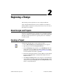
Chapter 2
Beginning a Design
About Designs and Projects........................................................................................... 2-1
Creating a Project ......................................................................................................... 2-1
Creating a Design ......................................................................................................... 2-2
Creating a Design from a Netlist File ........................................................................... 2-2
Import Netlist dialog box buttons .................................................................. 2-3
Working with Projects .................................................................................................. 2-3
Opening an Existing File .............................................................................................. 2-4
Viewing Gerber Files ..................................................................................... 2-4
Parameters Supported in Gerber Viewer ......................................... 2-7
Saving and Closing ....................................................................................................... 2-9
Saving Technology Specifications from a Design ....................................................... 2-9
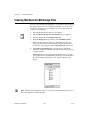
Loading Technology Files............................................................................................. 2-10
Selecting and Unselecting Elements ............................................................................ 2-10
Place and Select Modes ................................................................................................ 2-11
Searching for Design Elements .................................................................................... 2-12
Options for Viewing the Design.................................................................................... 2-13
Using the Full Screen ..................................................................................... 2-13
Magnifying and Shrinking the View .............................................................. 2-14
Refreshing the Design .................................................................................... 2-14
Tool-tip Label ................................................................................................. 2-14
NI Ultiboard User Manual
viii
ni.com
Contents
Chapter 3
Setting Up a Design
Working with Layers .....................................................................................................3-1
Defining Copper Layers .................................................................................3-1
Accessing Layers ............................................................................................3-3
Working with the Board Outline ..................................................................................3-5
Using the Drawing Tools to Create a Board Outline ......................................3-5
Importing a DXF File .....................................................................................3-6
Using a Pre-Defined Board Outline ...............................................................3-6
Using the Board Wizard .................................................................................3-6
Setting the Board’s Reference Point .............................................................................3-8
Enter coordinate dialog box ............................................................................3-9
Design Rule Errors ........................................................................................................3-9
Working with the Group Editor ....................................................................................3-11
Add Group dialog box ....................................................................................3-11
Working with Net Groups ..............................................................................3-11
Working with Part Groups ..............................................................................3-14
Working with Bus Groups ..............................................................................3-18
Working with Differential Pairs .....................................................................3-20
Change Group Settings dialog box .................................................................3-23
Net Group Settings ...........................................................................3-23
Part Group Settings ..........................................................................3-24
Differential Pair Settings ..................................................................3-24
Forward and Backward Annotation ..............................................................................3-24
Chapter 4
Working with Parts
Placing Parts ..................................................................................................................4-1
Dragging Parts from Outside the Board Outline .............................................4-1
Using the Parts Tab in the Spreadsheet View ................................................4-2
Using the Parts Tab to Place Parts ....................................................4-3
Using the Parts Tab for Other Functions ..........................................4-4
Tools to Assist Part Placement ........................................................................4-4
Working with Ratsnests ....................................................................4-5
Working with Force Vectors.............................................................4-6
Dragging Parts...................................................................................4-7
Shoving Parts ....................................................................................4-7
Using Ruler Bars and Guides............................................................4-10
Orienting Parts .................................................................................4-10
Aligning Shapes and Parts ...............................................................4-11
© National Instruments Corporation
ix
NI Ultiboard User Manual
Contents
Spacing Shapes and Parts ................................................................ 4-11
Placing a Group Array Box ............................................................. 4-12
Replicating Group Part Placement .................................................. 4-14
Unplacing Parts ............................................................................................... 4-16
Viewing and Editing Properties..................................................................................... 4-16
Attributes ........................................................................................................ 4-16
Viewing and Editing Part Properties .............................................................. 4-17
Part Properties: Position ................................................................... 4-18
Part Properties: 3D Data .................................................................. 4-18
Part Properties: Part .......................................................................... 4-20
Viewing and Editing Attributes ...................................................................... 4-20
Attributes: General ........................................................................... 4-20
Attributes: Position .......................................................................... 4-20
Attributes: Attribute.......................................................................... 4-20
Viewing and Editing Shape/Graphics Properties............................................ 4-21
Shape Properties: Attributes ............................................................ 4-21
Shape, Graphic, Attribute, Dimension, Through Hole Pin and
SMT Pin Properties: General ........................................................ 4-21
Shape, Graphic and Dimension Properties: Position ....................... 4-21
Shape/Graphic Properties: Arc, Line, Bezier, Circle, Ellipse,
Rounded Rectangle, Rectangle, Pie, Polygon ............................... 4-21
Placing Other Elements ................................................................................................. 4-22
Placing Mounting Holes and Connectors........................................................ 4-22
Placing Holes .................................................................................................. 4-22
Placing Shapes and Graphics .......................................................................... 4-23
Working with Jumpers .................................................................................... 4-24
Placing Jumpers ................................................................................ 4-24
Viewing and Editing Jumper Properties ........................................... 4-25
Jumper Properties: Attributes ........................................................... 4-25
Jumper Properties: Line.................................................................... 4-25
Jumper Properties: Jumper .............................................................. 4-25
Working with Test Points ............................................................................... 4-26
Placing Test Points ........................................................................... 4-26
Viewing and Editing Test Point Properties ...................................... 4-26
Working with Dimensions .............................................................................. 4-27
Placing Dimensions .......................................................................... 4-27
Viewing and Editing Dimension Properties ..................................... 4-27
Dimension Properties: Attributes ..................................................... 4-27
Dimension Properties: General ........................................................ 4-27
Dimension Properties: Position ....................................................... 4-28
Dimension Properties: Line ............................................................. 4-28
Dimension Properties: Dimensions ................................................. 4-28
Placing Parts from the Database ................................................................................... 4-29
NI Ultiboard User Manual
x
ni.com
Contents
Editing Parts and Shapes................................................................................................4-30
Editing a Placed Part (In-Place Edit) ..............................................................4-30
Editing a Polygon ............................................................................................4-32
Viewing and Editing Through Hole Pin Properties ........................................4-34
Attributes...........................................................................................4-34
General .............................................................................................4-34
Pad ....................................................................................................4-34
Layer Settings ..................................................................................4-35
Thermal Relief .................................................................................4-35
Viewing and Editing SMT Pin Properties .......................................................4-35
SMT Pin Properties: Attributes.........................................................4-35
SMT Pin Properties: General ............................................................4-35
SMT Pin Properties: Pad ..................................................................4-36
SMT Pin Properties: Thermal Relief ................................................4-36
SMT Pin Properties: Pin Neck .........................................................4-36
Searching For and Replacing Parts ................................................................................4-36
Searching for Parts in Open Designs...............................................................4-36
Locating a Part in a Design .............................................................................4-37
Replacing Parts................................................................................................4-37
Cross-probing.................................................................................................................4-37
Creating New Parts ........................................................................................................4-38
Using the Database Manager to Create a Part ................................................4-38
Using the Part Wizard to Create a Part ...........................................................4-39
Managing the Database .................................................................................................4-43
IPC-Compliant Land Patterns in Ultiboard ....................................................4-45
Working with Database Categories ................................................................4-50
Adding Parts to the Database ..........................................................................4-51
Adding Parts using the Database Manager ......................................4-51
Adding Parts using the Add Selection to Database Command ........4-52
Merging and Converting Databases...............................................................................4-52
Merging Databases .........................................................................................4-53
Converting Databases .....................................................................................4-53
Chapter 5
Working with Traces and Copper
Placing Traces................................................................................................................5-1
Placing a Trace: Manual Method ....................................................................5-2
Placing a Trace: Follow-me Method ...............................................................5-3
Placing a Trace: Connection Machine Method ...............................................5-4
Placing a Bus ...................................................................................................5-5
Working with Density Bars .............................................................................5-6
© National Instruments Corporation
xi
NI Ultiboard User Manual
Contents
Working with Keep-in/Keep-out Areas .......................................................... 5-7
Placing Keep-in/Keep-out Areas ...................................................... 5-7
Viewing and Editing Keep-in/Keep-out Properties.......................... 5-7
Keep-in/keep-out Properties: Keep-in/keep-out Tab........................ 5-7
Equi-Spacing Traces ....................................................................................... 5-8
Deleting a Trace .............................................................................................. 5-9
Working with Other Copper Elements .......................................................................... 5-9
Placing Copper Areas...................................................................................... 5-10
Placing Powerplanes ...................................................................................... 5-10
Splitting Copper .............................................................................................. 5-10
Converting a Copper Shape to an Area........................................................... 5-11
Deleting All Copper ........................................................................................ 5-12
Adding and Removing Teardrops .................................................................. 5-12
Viewing and Editing Copper Properties........................................................................ 5-12
Copper Properties: Attributes Tab .................................................................. 5-13
Copper Properties: General Tab...................................................................... 5-13
Copper Properties: Position Tab ..................................................................... 5-13
Copper, Jumper and Dimensions Properties: Line Tab .................................. 5-13
Copper Properties: Copper Area Tab.............................................................. 5-14
Working with Vias ........................................................................................................ 5-14
Placing Vias ................................................................................................... 5-15
Viewing and Editing Via Properties ............................................................... 5-15
Attributes Tab ................................................................................... 5-15
General Tab ...................................................................................... 5-15
Via Tab ............................................................................................ 5-16
Micro Via Tab ................................................................................. 5-17
Via Properties: Thermal Relief Tab.................................................. 5-17
Placing SMD Fanouts ................................................................................................... 5-18
Working with Nets ........................................................................................................ 5-19
Using the Nets Tab ......................................................................................... 5-19
Using the Netlist Editor .................................................................................. 5-20
Adding a Net .................................................................................... 5-21
Renaming a Net ............................................................................... 5-25
Deleting a Net .................................................................................. 5-25
Removing a Pin from a Net .............................................................. 5-26
Setting Net Widths ........................................................................... 5-26
Setting High Speed Parameters ....................................................... 5-26
Setting Miscellaneous Net Parameters ............................................ 5-27
Setting Group Parameters ................................................................ 5-27
Setting Via Parameters .................................................................... 5-28
Highlighting a Net........................................................................................... 5-28
Shielding Nets ................................................................................................ 5-28
NI Ultiboard User Manual
xii
ni.com
Contents
Net Bridges......................................................................................................5-30
Creating a Net Bridge .......................................................................5-30
Placing a Net Bridge .........................................................................5-32
Copying a Copper Route .................................................................................5-33
Swapping Pins and Gates...............................................................................................5-34
Swapping Pins .................................................................................................5-34
Swapping Gates ...............................................................................................5-35
Automatic Pin/Gate Swapping ........................................................................5-38
Real-Time Pin/Gate Swapping ........................................................................5-39
Chapter 6
PCB Calculators
PCB Transmission Line Calculator ..............................................................................6-1
Microstrip Trace Calculations .........................................................................6-2
Embedded Microstrip Trace Calculations .......................................................6-3
Centered Stripline Trace Calculations.............................................................6-4
Asymmetric Stripline Trace Calculations .......................................................6-5
Dual Stripline Trace Calculations ...................................................................6-6
PCB Differential Impedance Calculator .......................................................................6-7
Microstrip Calculations ...................................................................................6-8
Embedded Microstrip Calculations .................................................................6-9
Centered Stripline Calculations.......................................................................6-10
Asymmetric Stripline Calculations..................................................................6-12
Chapter 7
Autorouting and Autoplacement
Autoplacement of Parts..................................................................................................7-1
Pre-Placing Parts .............................................................................................7-1
Understanding How the Autoplacer Works ....................................................7-1
Running the Autoplacer...................................................................................7-2
Controlling the Autoplacer .............................................................................7-2
Strategies to Achieve Better Part Placement ...................................................7-4
Autorouting ....................................................................................................................7-5
Understanding How the Autorouter Works.....................................................7-5
Understanding the Four Fundamental Routing Functions...............................7-5
Router Preprocessing ........................................................................7-5
Initial Routing ...................................................................................7-6
Rip-up and Retry Routing .................................................................7-6
Optimization......................................................................................7-6
Routing Selected Parts and Nets......................................................................7-7
Running the Autorouter...................................................................................7-7
Interactivity .......................................................................................7-8
© National Instruments Corporation
xiii
NI Ultiboard User Manual
Contents
Autorouting buses ........................................................................................... 7-8
Placing Automatic Test Points ....................................................................... 7-9
Controlling the Routing Functions.................................................................. 7-10
Routing Options: General Tab ......................................................... 7-10
Routing Options: Cost Factors Tab ................................................. 7-11
Routing Options: Rip-Up Tab ......................................................... 7-13
Routing Options: Optimization Tab ................................................ 7-14
Routing Options: Bus Autorouting Tab ........................................... 7-15
Strategies to Achieve Better Routing Results ................................................. 7-16
Chapter 8
Preparing for Manufacturing/Assembly
Placing and Editing Text .............................................................................................. 8-1
Capturing Screen Area .................................................................................................. 8-2
Placing a Comment ....................................................................................................... 8-3
Renumbering Parts ....................................................................................................... 8-5
Mitering Corners .......................................................................................................... 8-7
Manually Re-Running the Design Rules and Netlist Check ......................................... 8-8
Cleaning up the Board ................................................................................................... 8-8
Deleting Open Trace Ends .............................................................................. 8-8
Deleting Unused Vias ..................................................................................... 8-9
Exporting a File ............................................................................................................ 8-9
Using Export Settings .................................................................................... 8-10
Viewing and Editing Export Properties .......................................................... 8-10
Setting Gerber Properties ................................................................. 8-11
Setting DXF Properties..................................................................... 8-12
Setting NC Drill Properties .............................................................. 8-12
Working with Scale Vector Graphics Properties.............................. 8-12
Working with other Properties ......................................................... 8-13
Exporting the Desired File .............................................................................. 8-15
Printing your Design ..................................................................................................... 8-15
Previewing the Printed Design ..................................................................................... 8-16
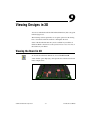
Chapter 9
Viewing Designs in 3D
Viewing the Board in 3D .............................................................................................. 9-1
Manipulating the 3D View ............................................................................................ 9-2
Controlling the Elements Viewed in 3D ......................................................... 9-3
Showing an Object’s Height ........................................................................... 9-4
Internal View................................................................................................... 9-5
Exporting to 3D DXF .................................................................................................... 9-6
Exporting to 3D IGES ................................................................................................... 9-6
NI Ultiboard User Manual
xiv
ni.com
Contents
Chapter 10
Using Mechanical CAD
Creating Mechanical CAD Projects...............................................................................10-1
Creating Mechanical CAD Design Files .......................................................................10-2
Importing a DXF File ......................................................................................10-3
Setting Mechanical CAD Properties and Options .........................................................10-3
Setting Mechanical CAD Properties ...............................................................10-3
Setting Mechanical CAD Colors ....................................................................10-3
Controlling Workspace Elements for Mechanical CAD .................................10-4
Setting Paths for Mechanical CAD .................................................................10-5
Setting Mechanical CAD Dimensions ............................................................10-5
Appendix A
Menus and Commands
File Menu ......................................................................................................................A-1
Edit Menu .....................................................................................................................A-3
View Menu ....................................................................................................................A-6
Place Menu ...................................................................................................................A-8
Design Menu .................................................................................................................A-12
Transfer Menu ...............................................................................................................A-14
Tools Menu ...................................................................................................................A-14
Autoroute Menu ............................................................................................................A-16
Options Menu ...............................................................................................................A-17
Window Menu ..............................................................................................................A-18
Help Menu ....................................................................................................................A-19
Context Menus ...............................................................................................................A-19
Select Menu ....................................................................................................A-19
Right-drag Menu .............................................................................................A-21
Place Trace Menu ............................................................................................A-21
Appendix B
Archiving Data
Backing up the Corporate Database...............................................................................B-1
Backing up the User Database and Configuration files .................................................B-2
Appendix C
Technical Support and Professional Services
Glossary
Index
© National Instruments Corporation
xv
NI Ultiboard User Manual
1
User Interface
The following sections explain the basic components of the Ultiboard
Graphical User Interface (GUI) and show how to set up user preferences
and PCB properties.
Some of the described features may not be available in your edition of
Ultiboard. Refer to the NI Circuit Design Suite Release Notes for a list of
the features in your edition.
Introduction to the Ultiboard Interface
Ultiboard is the PCB layout application of National Instruments Circuit
Design Suite, a suite of EDA (Electronics Design Automation) tools that
assists you in carrying out the major steps in the circuit design flow.
Ultiboard is used to design printed circuit boards, perform certain basic
mechanical CAD operations, and prepare them for manufacturing. It also
provides automated parts placement and layout.
For more information on the Ultiboard interface, and information on the other
components of NI Circuit Design Suite, refer to Getting Started with NI Circuit Design
Suite.
Note
Toolbars
The toolbars provide a quick, convenient way for you to access the most
common Ultiboard functions. You can toggle toolbars on and off using the
View»Toolbars menu.
© National Instruments Corporation
1-1
NI Ultiboard User Manual
Chapter 1
User Interface
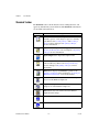
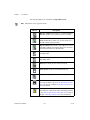
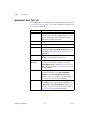
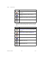
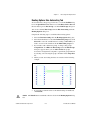
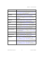
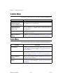
Standard Toolbar
The Standard toolbar contains buttons for basic editing functions, and
appears by default when you run Ultiboard. The Standard toolbar buttons
are described in the table below.
Button
Description
New File button. Creates a new project (if none are
currently open) or a new design if a project is currently
open. Refer to the Creating a Project and Creating a
Design sections of Chapter 2, Beginning a Design,
for more information.
Open File button. Opens an existing project. Refer to the
Opening an Existing File section of Chapter 2, Beginning
a Design, for more information.
Open Sample button. Opens the samples folder.
Save File button. Saves the active design to its current
name and directory. Refer to the Saving and Closing
section of Chapter 2, Beginning a Design, for more
information.
Print button. Displays the Print dialog. Refer to the
Printing your Design section of Chapter 8, Preparing for
Manufacturing/Assembly, for more information.
Cut button. Cuts the selected element from the design and
places it on the Windows Clipboard.
Copy button. Copies the selected element from the design
and places it on the Windows Clipboard.
Paste button. Pastes the element from the Windows
Clipboard to the design.
Undo button. Undoes the last action.
Redo button. Redoes the last action (used after undoing).
NI Ultiboard User Manual
1-2
ni.com
Chapter 1
User Interface
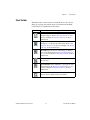
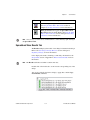
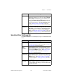
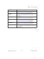
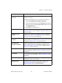
View Toolbar
The View toolbar contains buttons for modifying the way the screen is
displayed, and appears by default when you run Ultiboard. The View
toolbar buttons are explained in the table below.
Button
Description
Redraw the Screen button. Redraws the currently active
design workspace. Refer to the Refreshing the Design
section of Chapter 2, Beginning a Design, for more
information.
Toggle Full Screen button. Adjusts the size of the
workspace so it displays the entire design. Refer to the
Using the Full Screen section of of Chapter 2, Beginning
a Design, for more information.
Zoom In button. Zooms in on the design, providing a
closer view. Refer to the Magnifying and Shrinking the
View section of Chapter 2, Beginning a Design, for more
information.
Zoom Out button. Zooms out on the design, providing a
broader view.
Zoom Window button. Magnifies a selected part of the
design. Refer to the Magnifying and Shrinking the View
section of Chapter 2, Beginning a Design, for more
information.
Zoom Bounds button. Shows the entire design, including
objects that are outside of the board outline.
© National Instruments Corporation
1-3
NI Ultiboard User Manual
Chapter 1
User Interface
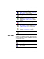
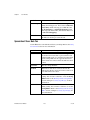
Main Toolbar
The Main toolbar contains buttons for common board design functions.
Its buttons are described in the table below.
Button
Description
Select button. De-activates any selected mode (for
example, for placing traces) and allows you to select an
element on the board.
Show or Hide Design Toolbox button. Shows or hides
the Design Toolbox. Refer to the Design Toolbox section
for more information.
Show or Hide Spreadsheet button. Shows or hides the
Spreadsheet View. Refer to the Spreadsheet View
section for more information.
Database Manager button. Displays the Database
Manager. Refer to the Managing the Database section of
Chapter 4, Working with Parts, for more information.
Board Wizard button. Launches the Board Wizard.
Refer to the Using the Board Wizard section of Chapter 3,
Setting Up a Design, for more information.
Part Wizard button. Starts the Part Wizard. Refer to the
Using the Part Wizard to Create a Part section of
Chapter 4, Working with Parts, for more information.
Place Part from Database button. Allows you to browse
the database for a part to place. Refer to the Placing Parts
from the Database section of Chapter 4, Working with
Parts, for more information.
Place Line button. Places a straight line on the design
(or places a trace, if the active layer is a copper one).
Refer to the Placing Shapes and Graphics section of
Chapter 4, Working with Parts, and the Placing a Trace:
Manual Method section of Chapter 5, Working with
Traces and Copper, for more information.
Follow-me button. Places a follow-me trace. Refer
to the Placing a Trace: Follow-me Method section of
Chapter 5, Working with Traces and Copper, for more
information.
NI Ultiboard User Manual
1-4
ni.com
Chapter 1
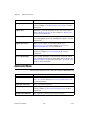
Button
User Interface
Description
Place Via button. Places a via on the design. Refer to the
Working with Vias section of Chapter 5, Working with
Traces and Copper, for more information.
Place Copper Area button. Places a copper area on the
design.
Create Power Plane button. Places a powerplane on the
design. Refer to the Placing Powerplanes section of
Chapter 5, Working with Traces and Copper, for more
information.
Design Rule Check button. Runs the Design Rule
Check and places results in the Results tab.
Place Text button. Places text on the design. Refer to the
Placing and Editing Text section of Chapter 8, Preparing
for Manufacturing/Assembly, for more information.
Show 3D button. Displays the current design in three
dimensions. Refer to the Viewing Designs in 3D section
of Chapter 9, Viewing Designs in 3D, for more
information.
Help button. Displays the Ultiboard Help.
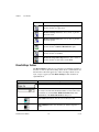
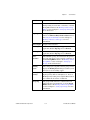
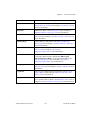
Select Toolbar
The Select toolbar contains the functions used to control selection filters,
and appears by default when you run Ultiboard. The Select toolbar buttons
are explained in the table below.
Button
Description
Enable Selecting Parts button. Use to allow or prevent
selection of parts.
Enable Selecting Traces button. Use to allow or prevent
selection of traces.
© National Instruments Corporation
1-5
NI Ultiboard User Manual
Chapter 1
User Interface
Button
Description
Enable Selecting Copper Areas button. Use to allow or
prevent selection of copper areas.
Enable Selecting Vias button. Use to allow or prevent
selection of vias.
Enable Selecting Pads button. Use to allow or prevent
selection of pads.
Enable Selecting SMD Pads button. Use to allow or
prevent selection of Surface Mount Device pads.
Enable Selecting Attributes button. Use to allow or
prevent selection of attributes.
Enable Selecting Other Objects button. Use to allow or
prevent selection of other object on the PCB.
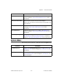
Draw Settings Toolbar
The Draw Settings toolbar lets you select the layer, thickness and unit of
measure of a line or object that is being drawn. It also contains buttons for
functions that control the appearance of lines and shapes drawn on any
layer, except a copper layer. The Draw Settings toolbar elements are
explained below.
Button
Description
Selects the layer for the line or object being drawn.
Sets the thickness and unit of measure of the line being drawn, or
of an object’s border. The maximum number of values that can be
stored here are set in the Line Width Cache Size field of the
General tab of the Global Preferences dialog box.
Select Fill Color button. Sets the color of the layer’s fill.
Select Fill Style button. Sets the fill style, either transparent or
solid.
NI Ultiboard User Manual
1-6
ni.com
Chapter 1
Button
User Interface
Description
Select Line Color button. Sets the color of the layer’s line.
Select Line Type button. Sets the lines style, for example, solid,
dashed.
Edit Toolbar
The Edit toolbar contains the functions used for editing specific elements,
including in-place editing and orientation. The Edit toolbar buttons are
explained in the table below.
Button
Description
Toggle In-Place PCB Part Edit button. Activates
In-Place Edit for placed PCB parts. Refer to the Editing
a Placed Part (In-Place Edit) section of Chapter 4,
Working with Parts, for more information.
Toggle In-Place Edit Text or Attribute button.
Allows you to edit the selected text.
Rotate Clockwise button. Rotates selected item
clockwise. Refer to the Orienting Parts section of
Chapter 4, Working with Parts, for more information.
Rotate Counter Clockwise button. Rotates selected item
counter-clockwise. Refer to the Orienting Parts section
of Chapter 4, Working with Parts, for more information.
Swap Layer button. Places a part on mirror layer. Refer
to the Orienting Parts section of Chapter 4, Working with
Parts, for more information.
Align Toolbar
The Align toolbar contains the functions used to align and space design
elements. Refer to the Aligning Shapes and Parts and Spacing Shapes and
Parts sections of Chapter 4, Working with Parts, for more information.
© National Instruments Corporation
1-7
NI Ultiboard User Manual
Chapter 1
User Interface
The Align toolbar buttons are explained in the table below.
Button
Description
Align Left button. Aligns the left sides of the selected
parts.
Align Right button. Aligns the right sides of the selected
parts.
Align Top button. Aligns the top edges of the selected
parts.
Align Bottom button. Aligns the bottom edges of the
selected parts.
Align Center Horizontal button. Shifts the selected
elements horizontally so their centers are aligned.
Align Center Vertical button. Shifts the selected
elements vertically so their centers are aligned.
Space Across button. Spaces three or more objects beside
each other evenly.
Space Across Plus button. Increases horizontal space
between two or more objects.
Space Across Min button. Decreases horizontal space
between two or more objects.
Space Down button. Spaces three or more objects above
each other evenly.
Space Down Plus button. Increases vertical space
between two or more objects.
Space Down Min button. Decreases vertical space
between two or more objects.
NI Ultiboard User Manual
1-8
ni.com
Chapter 1
User Interface
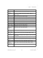
Place Toolbar
The Place toolbar contains the functions used to place elements such as
traces, lines and polygons on the design. The Place toolbar buttons are
explained in the table below.
Button
Description
Place Comment button. Places a comment on the design.
Refer to the Placing a Comment section of Chapter 8,
Preparing for Manufacturing/Assembly, for more
information.
Capture Area button. Captures a section of the screen
and places it on the system clipboard.
Select button. De-activates any selected mode (for
example, for placing traces) and allows you to select an
element on the board.
Place Line button. Places a line on the design (or place a
trace, when used on a copper layer). Refer to the Placing
Shapes and Graphics section of Chapter 4, Working with
Parts, for more information.
Place Arc button. Places an arc on the design. Refer to the
Placing Shapes and Graphics section of Chapter 4,
Working with Parts, for more information.
Place Elliptical Arc button. Left-click two points to draw
an elliptical arc between them, then move the pointer to
change the degree of arc.
Refer to the Placing Shapes and Graphics section of
Chapter 4, Working with Parts, for more information.
Place Bezier button. Places a bezier curve on the design.
Refer to the Placing Shapes and Graphics section of
Chapter 4, Working with Parts, for more information.
Place Circle button. Places a circle on the design. Refer
to the Placing Shapes and Graphics section of Chapter 4,
Working with Parts, for more information.
Place Ellipse button. Places an ellipse on the design.
Refer to the Placing Shapes and Graphics section of
Chapter 4, Working with Parts, for more information.
© National Instruments Corporation
1-9
NI Ultiboard User Manual
Chapter 1
User Interface
Button
Description
Place Pie button. Places a pie-shape on the design. Refer
to the Placing Shapes and Graphics section of Chapter 4,
Working with Parts, for more information.
Place Rounded Rectangle button. Places a rectangle
with rounded corners. Refer to the Placing Shapes and
Graphics section of Chapter 4, Working with Parts, for
more information.
Place Rectangle button. Places a rectangle on the design.
Refer to the Placing Shapes and Graphics section of
Chapter 4, Working with Parts, for more information.
Place Polygon button. Places a polygon on the design.
Refer to the Placing Shapes and Graphics section of
Chapter 4, Working with Parts, for more information.
Place Copper Area button. Places a polygon copper area
on the design. Refer to the Placing Copper Areas section
of Chapter 5, Working with Traces and Copper, for more
information.
Follow-me button. Places a follow me trace, a trace that
automatically draws a legal trace between two selected
points. Refer to the Placing a Trace: Follow-me Method
section of Chapter 5, Working with Traces and Copper,
for more information.
Place Multiple Traces as a Bus button. Use to connect
multiple traces between multi-pinned devices such as ICs.
Refer to the Placing a Bus section of Chapter 5, Working
with Traces and Copper, for more information.
Place Group Array Box button. Uses a group array box
to place parts in an array. Refer to the Placing a Group
Array Box section of Chapter 4, Working with Parts, for
more information.
Place Text button. Places text on the design. Useful for
annotation purposes. Refer to the Placing and Editing
Text section of Chapter 8, Preparing for
Manufacturing/Assembly, for more information.
NI Ultiboard User Manual
1-10
ni.com
Chapter 1
Button
User Interface
Description
Place a Standard Dimension button. Places a dimension
between any two selected points. Refer to the Working
with Dimensions section of Chapter 4, Working with
Parts, for more information.
Place a Horizontal Dimension button. Places a
horizontally-oriented dimension between two selected
points. Refer to the Working with Dimensions section of
Chapter 4, Working with Parts, for more information.
Place a Vertical Dimension button. Places a
vertically-oriented dimension between two selected
points. Refer to the Working with Dimensions section of
Chapter 4, Working with Parts, for more information.
Place a Net Bridge button. Places a net bridge
connection. Refer to the Net Bridges section of Chapter 5,
Working with Traces and Copper, for more information.
Place a Hole button. Places a hole on your PCB.
Place a Via button. Places a via on the design. Refer to
the Working with Vias section of Chapter 5, Working with
Traces and Copper, for information.
Place Pins button. Places pins on the design when editing
or creating a part in In-place Edit mode or Footprint
Edit mode. Refer to the Editing a Placed Part (In-Place
Edit) and Using the Database Manager to Create a Part
sections of Chapter 4, Working with Parts, for more
information.
Polygon Splitter button. Splits copper areas and
powerplanes. Refer to the Splitting Copper section of
Chapter 5, Working with Traces and Copper, for more
information.
Remove Copper Islands button. Removes copper
islands. Refer to the Placing Copper Areas section of
Chapter 5, Working with Traces and Copper, for more
information.
© National Instruments Corporation
1-11
NI Ultiboard User Manual
Chapter 1
User Interface
Wizard Toolbar
The Wizard toolbar contains the wizard functions supported by Ultiboard.
The Wizard toolbar buttons are explained in the table below.
Button
Description
Board Wizard button. Starts the Board Wizard. Refer
to the Working with the Board Outline section of
Chapter 3, Setting Up a Design, for more information.
Part Wizard button. Starts the Part Wizard. Refer to the
Using the Part Wizard to Create a Part section of
Chapter 4, Working with Parts, for more information.
Autoroute Toolbar
The Autoroute toolbar contains the autorouting and placement functions
supported by Ultiboard. The Autoroute toolbar buttons are explained in
the table below.
Button
Description
Begin Autoplacing button. Starts automatically placing
parts.
Autoroute Selected Buses button. Displays the Bus
Autorouting dialog.
Start Trace Optimization button. Starts trace
optimization.
Start/Resume Autorouting button. Starts placing traces,
or continues placing traces if the autorouter was paused.
Stop/Pause Autorouter button.
NI Ultiboard User Manual
1-12
ni.com
Chapter 1
User Interface
Locking Toolbars
You can lock toolbars in place to prevent them from being inadvertently
moved.
Once you have placed them as you like, you can lock all docked toolbars in
place in different ways: Select Options»Lock Toolbars.
•
Enable Lock all docked toolbars from the Toolbars tab of the
Customize dialog box. Refer to the Toolbars Tab section for more
information.
•
Right-click in any toolbar and select Lock Toolbars from the context
menu that appears.
If the Lock Toolbars option is enabled, floating toolbars will be locked in place if
you move them to a docked position.
Note
To drag a docked toolbar to a different location when Lock Toolbars is enabled, hold
down <Alt> and drag the toolbar with your mouse.
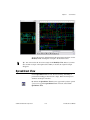
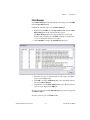
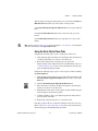
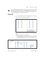
Tip
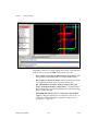
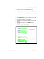
When Lock Toolbars is disabled, the drag bars on all docked toolbars
display, as shown in the figure below (1). Grab the toolbar by the drag bar
to move it.
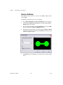
1
Note
Drag Bar
If the Lock Toolbars option is enabled, the drag bars do not appear.
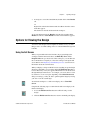
Toolbar Behavior When Ultiboard Size is Reduced
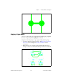
If you reduce the size of Ultiboard, some of the buttons in larger toolbars
may become hidden. If this happens, the More buttons icon appears as
shown in the figure below (1).
1
More Buttons Icon
Click the More Buttons icon to display the hidden buttons.
© National Instruments Corporation
1-13
NI Ultiboard User Manual
Chapter 1
User Interface
Text boxes and drop-down lists do not display when Ultiboard’s size is reduced. To
show these, make Ultiboard large enough to show all toolbar buttons without the More
buttons icon.
Note
You can make your own toolbars and add or delete buttons from existing toolbars to
get everything to fit. Refer to the Toolbars Tab section for more information.
Tip
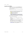
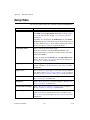
Setting Global Preferences
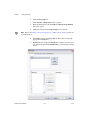
This section explains general procedures for setting global preferences. The
following sections describe details of setting specific options.
Complete the following steps to set your user preferences:
1.
Choose Options»Global Preferences. The Global Preferences
dialog box appears, with the following tabs:
•
General Tab
•
Paths Tab
•
Message Prompts Tab
•
Colors Tab
•
PCB Design Tab
•
Dimensions Tab
•
3D Options Tab
2.
Select the desired tab.
3.
Set the desired options. The specific options and settings available in
the tabs are described in the following sections.
4.
Click OK to save your changes.
General Tab
Complete the following steps to change workspace options:
NI Ultiboard User Manual
1.
Choose Options»Global Preferences and select the General tab.
2.
Set the Full Screen mode, View, Crosshair and Mouse wheel
behavior settings as desired.
3.
Set the following as desired:
•
Auto save settings—Enable to have changes automatically saved
at the specified Time interval.
•
Minimum control point size—The size of the control points on
vertices and other objects.
1-14
ni.com
Chapter 1
4.
User Interface
•
Line width cache size—The number of recently used line widths
Ultiboard keeps in memory. Minimum cache size is 5.
•
Undo buffer size—The number of undo actions allowed.
•
Load last file on startup—Enable if you would like to continue
working on the last file you had open in your previous Ultiboard
session.
•
Unicode settings box—If desired, enable the Save .TXT files as
plain text checkbox.
•
Language—Select the desired language from the list. You must
restart Ultiboard for all dialog boxes to reflect the new setting.
To apply your changes but leave the Global Preferences dialog box
open, click Apply. To apply your changes and close the Global
Preferences dialog box, click OK.
Paths Tab
The Ultiboard installation puts specific files in specific locations. If
necessary you can point Ultiboard to a new location to find, for example,
database files. You can also use this dialog box to create and specify user
settings files that contain individuals’ preferences for all options.
Complete the following steps to change file locations:
1.
Choose Options»Global Preferences. The Global Preferences
dialog box appears.
2.
Select the Paths tab.
3.
Change the settngs in the General area as desired:
4.
5.
© National Instruments Corporation
•
Circuit Default Path—This is where all new files are saved,
unless you manually navigate to a new location when saving.
•
User Button Images Path—This is where you store any
user-created button graphics.
Change the User Settings as desired:
•
Configuration File—The location of the configuration file. This
file contains the user interface settings.
•
New User Configuration File—Click to create a new user
configuration file and select an item from the drop-down list.
Change the settings in the Database Files area as desired:
•
Master Database—The location of the Master Database.
•
Corporate Database—The location of the Corporate Database.
•
User Database—The location of the User Database.
1-15
NI Ultiboard User Manual
Chapter 1
User Interface
Message Prompts Tab
Use this tab to set the prompts you want to display in the described
situation.
Complete the following steps to set the dialog boxes that you want to
display in the described situation:
1.
Choose Options»Global Preferences to display the Global
Preferences dialog box.
2.
Select the Message prompts tab.
3.
Select the desired prompts’ checkboxes.
4.
Click OK.
Colors Tab
Use this tab to set up color schemes for the workspace background and
other displayed elements.
Complete the following steps to set up color schemes:
NI Ultiboard User Manual
1.
Choose Options»Global Preferences. The Global Preferences
dialog box appears.
2.
Select the Colors tab and complete the following as required:
•
To apply an existing color scheme, either the default or one you
have created, choose it from the Color scheme drop-down list.
•
To modify an existing color scheme, choose it from the Color
scheme drop-down list. (You cannot modify the Default Layout
Colors scheme.) From the Color element drop-down list, choose
the element whose color you want to modify. Click the color
button (unlabelled) and choose a new color for that element. Your
change is stored with the color scheme when you click Apply
or OK.
•
To create a color scheme, click New scheme and provide a scheme
name. The element colors remain at the value they had in the most
recently loaded scheme. Modify the element colors as described
above.
•
To delete a Color scheme, select it and click Delete. (You cannot
delete the Default Layout Colors scheme.)
•
To add a Color element, click New element and enter a name.
The element appears in the Color element list— choose a color
for the element as described earlier. (You cannot add a new
element to the Default Layout Colors scheme.)
1-16
ni.com
Chapter 1
User Interface
•
To delete a Color element, select it and click Delete. (You cannot
delete a default Color element.)
•
Optionally, enable the Preview grayed out checkbox to switch
the preview visibility on or off and adjust and select the Grayed
out factor.
Your changes are reflected in the Preview area.
3.
To apply your changes but leave the Global Preferences dialog box
open, click Apply. To apply your changes and close the Global
Preferences dialog box, click OK.
PCB Design Tab
Use this tab to define a variety of actions associated with the overall PCB
design.
Complete the following steps to define the default actions:
1.
Choose Options»Global Preferences. The Global Preferences
dialog box appears.
2.
Select the PCB design tab.
3.
Select the unit of measurement from the Units drop-down list.
4.
Set the viewing options in the View area:
5.
•
Show pin 1 mark—Select to display pin 1 of a device with a
unique marking.
•
Show copper areas—Select to display copper areas. This applies
to copper areas only, not regular polygon shapes on non-copper
layers.
•
Show pin info in pin—Select to display the pin number and hole
size when zoomed in.
In the On select entire trace area:
•
6.
© National Instruments Corporation
Select across layers—Select so that when you choose
Edit»Select Entire Trace, the trace is selected across all layers,
instead of just the active layer.
In the Part Drag area:
•
Re-route after move—Select if you would like the traces that are
attached to a part to be re-routed if you move the part.
•
Re-route fixed traces—Becomes active if Re-route after move
is selected. When selected, allows the autorouter to re-route traces
designated as “fixed.”
1-17
NI Ultiboard User Manual
Chapter 1
User Interface
7.
8.
9.
In the Default pin diameters area:
•
Jumpers—Enter the default pin diameter for jumpers.
•
Testpoints—Enter the default pin diameter for testpoints.
In the Action on DRC error area, set the actions to be taken when
Ultiboard encounters a Design Rule Error:
•
Cancel the current action—Select to prevent the current
operation from being completed. For example, placing a trace
over a pad that is part of a different netlist will not be permitted.
•
Ask for confirmation—Select so that if an invalid operation is
attempted a prompt is given asking if the operation should be
completed even though a Design Rule will be violated.
•
Overrule—Select to permit the operation to be completed.
In the On trace deletion area:
•
Auto delete via (standard)—Select to have vias automatically
deleted when you delete the trace associated with that via.
•
Auto delete teardrop—Select to have teardrops automatically
deleted when you delete the trace associated with that teardrop.
10. In the On trace placement area:
•
Auto trace narrowing—Select to allow traces to narrow as
necessary during routing.
•
Auto add teardrop—Select to add a teardrop when a trace is
placed.
11. In the DRC & Net check area:
•
No realtime check—Select to prevent a DRC and netcheck in
“real time” as you place objects, for example, parts.
•
Check on action end—Select to perform a DRC and netcheck
after each action, for example, part placement.
•
Full realtime check—Select to perform DRC checks and ratnest
updates to your work in “real time” (as you place objects, for
example, parts).
12. In the Follow me router area:
•
Continuous placement—Select to have the next trace begin from
the finish point of the previous trace when placing a “Follow-me”
trace. If this is not selected, you must click to start a new trace.
Refer to the Placing a Trace: Follow-me Method section in Chapter 5,
Working with Traces and Copper, for information about Follow-me
traces.
NI Ultiboard User Manual
1-18
ni.com
Chapter 1
User Interface
13. In the Crosshair area:
•
Trace snap—Select to have the pointer snap to the nearest trace.
14. In the Automatic fiducial marks area:
•
Show fiducial marks—Select to show fiducial marks when you
postprocess this design.
•
Line thickness—Enter the desired thickness for the fiducial
marks’ lines.
Fiducial marks are used to align layers with each other. As shown
in the figure below, Ultiboard uses three different types of
cocentric circles as fiducial marks. These are placed on three of
the four corners of a design when it is printed or exported to
Gerber.
15. To apply your changes but leave the Global Preferences dialog box
open, click Apply. To apply your changes and close the Global
Preferences dialog box, click OK.
Dimensions Tab
Use the Dimensions tab to define the characteristics to be used for any
dimensions placed in the board. Refer to the Working with Dimensions
section of Chapter 4, Working with Parts, for information about placing
dimensions.
Complete the following steps to define the default dimension
characteristics:
1.
Choose Options»Global Preferences. The Global Preferences
dialog box appears.
2.
Click the Dimensions tab.
© National Instruments Corporation
1-19
NI Ultiboard User Manual
Chapter 1
User Interface
3.
Set the following as desired:
•
Units—This is the unit of measure for Stub length, Arrow style
and Text style.
•
Stub length—This is the amount the end lines of the dimension
protrude above eacg arrowhead.
•
Arrow style—This is where you adjust the size and appearance of
the arrow.
•
Text Style—This is where you adjust the size and appearance of
the text.
•
Displayed unit—Select the unit of measure to be displayed with
the dimension. If you select Use Design Settings, the unit of
measure selected in the Design Units field of the Grids & units
tab of the PCB Properties dialog box are used. This setting also
appears in the Draw Settings toolbar.
•
Alignment and Position—These are where you set how the text
appears in relation to the arrow.
•
Orientation—This is where you select the angle at which the
dimension displays.
The results of your choices display in the preview area of the tab.
4.
To apply your changes without closing the dialog box, click Apply.
Existing dimensions are not affected. To apply your changes and close
the dialog box, click OK.
3D Options Tab
Complete the following steps to set the 3D Viewer options:
NI Ultiboard User Manual
1.
Choose Options»Global Preferences and select the 3D Options tab.
2.
To change the background color in the 3D Viewer, click the
Background color button. The Color dialog box appears.
3.
Select the desired color and click OK in the Color dialog box.
4.
Optionally, enable the Show copper and silkscreen while moving
checkbox.
5.
Set the Internal view options as desired:
•
Use normal board thickness checkbox—Disables the option to
change Thickness for each layer and Spacing between layers.
•
Thickness for each layer—How wide each layer appears in the
Internal View.
•
Spacing between layers—The more space that you set between
the layers, the easier they will be to view when you zoom in on the
PCB in the 3D mode.
1-20
ni.com
Chapter 1
User Interface
Refer to the Internal View section of Chapter 9, Viewing Designs in 3D, for more
information.
Tip
6.
To apply your changes but leave the Global Preferences dialog box
open, click Apply. To apply your changes and close the Global
Preferences dialog box, click OK.
Setting PCB Properties
Many characteristics of your PCB design are controlled through the PCB
Properties dialog box including the number of layers, design rules and grid
settings. These settings are saved with the design and will be in effect when
the design is reopened.
Do one of the following to display the PCB Properties dialog box for the
board:
•
With nothing selected on the board, right-click on an empty portion of
the board and choose Properties from the context menu that appears.
•
Click on an empty portion of the board and choose Edit»Properties.
•
Double-click on an empty portion of the board.
Attributes Tab
All properties dialog boxes for all design elements have an Attributes tab,
although a design’s PCB typically does not have any attributes. Refer to the
Attributes section of Chapter 4, Working with Parts, for information about
adding attributes.
Grid & Units Tab
Use the Grid & units tab of the PCB Properties dialog box to control
Ultiboard grids and set the unit of measurement for your design.
Complete the following steps to set up the grid properties:
1.
Choose the default units of measure from the Design units list.
2.
In the Grid area, set the following elements as desired:
© National Instruments Corporation
•
Grid type—Select Standard grid for a rectangular grid, or Polar
grid, for a circular grid.
•
Visible grid style—This is where you set the style for the Visible
grid. (The Visible grid provides a visual reference for you to
align parts and traces.)
1-21
NI Ultiboard User Manual
Chapter 1
User Interface
3.
•
Visible grid—This is the distance between the grid’s elements
(dots, lines or crosses) that you set up in the Visible grid style
field.
•
Grid step name—Use this field to change the distance between a
grid’s elements. Select the desired grid: Part grid; Copper grid;
Via grid; SMD grid, and then enter the desired increment in the
Grid step value field.
•
Degree step—This field becomes active when Polar grid is
selected in the Grid type field. Enter the desired distance between
the grid’s elements (dots, lines or crosses). Select the unit of
measure in the drop-down list to the right of this field—choices
are: degrees, radians, or grads.
•
Grid start offset—This field becomes active when Polar grid is
selected in the Grid type field. Enter the distance to offset the
center of the polar grid: X is horizonatal offset; Y is vertical offset.
Click OK to close the dialog.
To show or hide the visible grid, select View»Grid.
Copper Layers Tab
Use the Copper layers tab of the PCB Properties dialog box to determine
the layer pairs that are acceptable for blind, buried or micro vias. This is
used when you try to place a via. Your choices will affect the cost of the
board, and should be confirmed with the board manufacturer.
This tab also allows you to set the default clearance for the board—the
distance from the edge of the board that is to be kept free of any other
elements. For example, if you try to run a trace through a clearance, or try
to place a part so that a pad is put within a clearance, a design rule error
occurs.
If you used the Board Wizard, the layer information and clearance may already
have been set. Refer to the Using the Board Wizard section of Chapter 3, Setting Up a
Design, for more information.
Note
Complete the following steps to set up the Copper layers tab:
NI Ultiboard User Manual
1.
Set the number of layer pairs you intend to use by entering the value or
using the up/down arrows in the Layer pairs field. There should be at
least one layered pair to act as a core.
2.
Set the number of Single layer stack-ups for both the top and bottom.
1-22
ni.com
Chapter 1
User Interface
3.
Select the Micro vias, Buried vias, or Blind vias checkboxes to use
these in your design.
4.
As you make changes to the layer settings, the Allowed vias pane
shows the acceptable layer combinations for blind and buried vias or
microvias. Use the checkboxes to select the layer combinations you
want to allow in your design.
5.
In the Allow routing area, from the Copper layer drop-down list,
select the copper layer for which you wish to assign routing properties
and click Properties to display the Copper Layer Properties dialog
box.
a.
Enable the Routing checkbox to allow routing on the selected
layer.
b.
In the Trace bias drop-down list, select one of Horizontal,
Vertical, or None.
c.
Click OK to close the Copper Layer Properties dialog box.
6.
In the Board area, enter the desired Board outline clearance and
Board thickness.
7.
Click OK to close the dialog box.
Pads/Vias Tab
Use the Pads/Vias tab of the PCB Properties dialog box to set the
following:
•
Through Hole Pad Annular Ring
•
Vias
•
Microvias
•
Maximum Vias Per Net
•
Surface Mount Pads Oversize
Through Hole Pad Annular Ring
Footprints in the database have been designed with pad sizes in accordance
with the manufacturers’ recommendations. To change these settings you
can edit the footprint in the database or directly on the design using the
In-place Part Edit command. Alternatively, you can apply a set of design
rules to specific footprints or to the entire design.
© National Instruments Corporation
1-23
NI Ultiboard User Manual
Chapter 1
User Interface
The annular ring setting (the ring of copper around the drill hole of a pad or
via) allows you to specify either a fixed value (for example, 50 mils) or a
relative value that depends on the radius of the drill hole size. For example,
a 50 mil drill hole (radius of 25 mils) with a relative value of .6 (60%)
creates an annular ring of 15 mils (60% of 25 mils). When using relative
settings, it is important to choose minimum and maximum values to ensure
that the annular ring never goes beyond those bounds.
Complete the following to enter an annular ring setting:
1.
Click the button beside the desired field (Top, Inner or Bottom) in the
Pad/Vias tab. The Through Hole Pad Properties dialog box appears.
a.
Choose Fixed and enter the fixed value.
Or
Choose Relative and enter the relative setting. Be sure to choose
Minimum and Maximum values.
Complete the following to apply the design rules to a footprint:
1.
Select the footprint and choose Edit»In-Place Part Edit.
2.
Select the pads to which the rule should apply.
3.
Right-click and, from the context menu, choose Properties.
4.
On the Pad tab of the properties dialog box, enable Use design rules.
Vias
Use the Vias area to set the default Drill diameter and Pad diameter to be
used when a via is placed during trace placement. This setting also applies
to vias that have already been placed in the design.
Microvias
Use the Micro vias area to set the default via dimensions to be used when
a microvia is placed during trace placement. These settings also apply to
microvias that have already been placed in the design.
The Capture land diameter field determines the land diameter where the
microvia starts, while Target land diameter determines the diameter
where the microvia ends. These terms are in accordance with the IPC and
JPCA joint standard IPC/JPCA-2315, Design Guide for High Density
Interconnects (HDI) and Microvias. The Maximum layer span is either
one or two layers.
NI Ultiboard User Manual
1-24
ni.com
Chapter 1
User Interface
Maximum Vias Per Net
Use the Nets area to set up the maximum number of vias allowed per net.
Surface Mount Pads Oversize
Depending on the manufacturing process you are using, you may wish to
enlarge the size of all surface mount pads by a fixed amount. This can be
set independently for the Top and Bottom layers. The setting refers to
the amount that will be added to the pad. In the case of a circular pad this
amount is added to the radius. In the case of a rectangular or square pad the
amount will be added to the width and length.
General Layers Tab
Use the General layers tab of the PCB Properties dialog box to control
which layers are available on the board.
Complete the following steps to control the numbers of layers in the board:
1.
Add layers to the board by selecting the checkbox beside the layer
name.
2.
Remove layers from the board by clearing the checkbox beside the
layer name.
You can have a layer available on the board, and temporarily dim or hide it. Refer to
the Accessing Layers section of Chapter 3, Setting Up a Design, for more information.
Note
There are up to 10 mechanical CAD layers in PCB design. These layers allow you
to provide information that is directly related to the PCB. You place elements on them to
represent the mechanical elements of your design—for example, cabinet casing or
mounting brackets.
Note
Complete the following steps to rename layers:
1.
Click Rename in the Layer names area. The Select Layer for
Renaming dialog box appears.
2.
Select the layer that you wish to rename and click OK. The Layer
dialog box appears.
3.
Enter the new Layer name and click OK.
© National Instruments Corporation
1-25
NI Ultiboard User Manual
Chapter 1
User Interface
Design Rules Tab
Complete the following steps to set the design rules for the PCB:
1.
Click the Design rules tab.
2.
In the Design rule default values area, set the following as desired:
•
Trace Width Settings—Set trace width and minimum and
maximum trace width.
•
Trace Length Settings—Set minimum and maximum trace
length.
•
Trace Neck Settings—Set minimum and maximum trace neck
length.
•
Clearance Settings—Set clearance to traces, pads, vias and
copper areas. For all of these clearances to be active, and display
in the Spreadsheet View, the Use multiple clearances checkbox
must be selected. Otherwise, only clearance to traces will be
operational.
•
Part Spacing Settings—Set minimum distance between parts.
This setting only applies to the spacing during part shoving.
To set this option for an individual part, go to the Part tab of that part’s properties
dialog box. Refer to the Shoving Parts section of Chapter 4, Working with Parts, for more
information.
Tip
•
Pin & Gate Swapping Settings—Set parameters for pin and gate
swapping.
•
Thermal Relief—Set the thermal relief shape.
•
Drill Technology—Set the minimum tool size for slot drilling.
Tip For information on any setting, select it in the Design rule default values area.
A description appears in the field at the bottom of the dialog.
Setting Favorite Layers
You can assign shortcuts for up to 10 layers using the Favorite layers tab.
These shortcuts can then be used to make a layer active. The active layer is
the layer where any new elements will be placed, or where any deletions
will be made.
Complete the following steps to assign shortcut numbers to layers:
1.
NI Ultiboard User Manual
Click on the Favorite layers tab.
1-26
ni.com
Chapter 1
User Interface
2.
Select the desired layer from the drop-down list beside each layer
number. For example, you may wish to assign Layer 2 to the
Copper Bottom layer.
3.
Click OK.
To make a layer active, press <Ctrl-Alt-layer number> on your keyboard.
The layer becomes active and is highlighted in the Layers tab of the Design
Toolbox.
In the above example, pressing <Ctrl-Alt-2> on your keyboard makes the
Copper Bottom layer active.
Design Toolbox
The Design Toolbox, shown in the figure below, is a vital part of the user
interface. You will use it often to manage your design efforts by controlling
major parts of Ultiboard’s functionality. To toggle it on or off, select
View»Design Toolbox.
© National Instruments Corporation
1-27
NI Ultiboard User Manual
Chapter 1
User Interface
The Design Toolbox is made up of two tabs:
•
The Projects tab lets you view the projects that are currently open.
Each project may contain one or more designs. Double-click to make
a particular design the current view.
You can change the order of the files shown in the Design tab by dragging and
dropping them. This does not change the order of the open design tabs that displays when
you have more than one design open. You can also drag and drop them to change their
order.
Tip
•
The Layers tab lets you move between layers of your design, control
the appearance of layers, and perform several other functions.
Birds Eye View
The Birds Eye View shows you the design at a glance and lets you easily
navigate around the workspace.
To magnify a specific area on the design, drag a rectangle around the
desired area on the Birds Eye View. The rectangle snaps to the same ratio
as the design space.
Note All layers appear in the Birds Eye View, whether or not they have been disabled in
the Layers tab of the Design Toolbox.
In the example in the figure below, the green rectangle that was drawn
encloses the four ICs in the middle of the Birds Eye View, and the design
has magnified to display only the items that are selected within this
rectangle.
NI Ultiboard User Manual
1-28
ni.com
Chapter 1
User Interface
To move the rectangle, hold down the right mouse button anywhere over the
Birds Eye View, and drag the rectangle to the desired location.
You cannot resize the selection rectangle in the Birds Eye View. Instead, you must
draw another rectangle of the required size. When you do this, the original rectangle
disappears.
Tip
Spreadsheet View
Use the Spreadsheet View for fast advanced viewing and editing of
parameters including part details such as shape, Reference Designators,
attributes and design constraints.
By default, the Spreadsheet View does not appear until you have opened
a project. To toggle the Spreadsheet View on and off, select View»
Spreadsheet View.
© National Instruments Corporation
1-29
NI Ultiboard User Manual
Chapter 1
User Interface
The following buttons are available in the Spreadsheet View.
Note
The buttons do not appear in all tabs.
Button
Description
Export to Textfile button. Displays a standard Windows
Save dialog where you save the selection as a textfile.
Export to CSV File button. Displays a standard
Windows Save dialog where you save the selection as a
file with comma-separated values.
Export to Excel button. Click to open a Microsoft® Excel
spreadsheet with the selected data displayed. (You must
have Excel installed to use this function.)
Sort Ascending button. Sorts the selected column in
ascending order.
Sort Descending button. Sorts the selected column in
descending order.
Print button. Prints the data in the selected tab.
Select All button. Selects all elements in the tab.
Copy button. Copies the selection to the clipboard.
Find and Select the Part button. Zooms in on the
selected part. Refer to the Using the Parts Tab for Other
Functions section of Chapter 4, Working with Parts, for
more information.
Lock the Selected Part button. Locks the selected
unlocked parts or unlocks the selected locked parts. Refer
to the Using the Parts Tab for Other Functions section of
Chapter 4, Working with Parts, for more information.
NI Ultiboard User Manual
1-30
ni.com
Chapter 1
Button
User Interface
Description
Start Placing the Unpositioned Parts button. Refer to
the Using the Parts Tab to Place Parts section of
Chapter 4, Working with Parts, for more information.
Show preview button. Toggles the Spreadsheet View
Preview function on and off. Refer to the Using the Parts
Tab for Other Functions section of Chapter 4, Working
with Parts, for more information.
You can also access the above commands from a context menu by right-clicking in
the Spreadsheet View.
Note
Spreadsheet View: Results Tab
The Results tab displays the results of searching for elements in the design.
Refer to the Searching for Design Elements section of Chapter 2,
Beginning a Design, for more information.
It also displays the results of running a connectivity check. Refer to the
Design Menu section of Appendix A, Menus and Commands, for more
information.
Note
The Results tab flashes red when it contains new data.
Double-click a line in this tab to zoom in on the corresponding area of the
design.
You can also right-click an item to display a popup that contains Copy,
Clear Results, and Go to.
© National Instruments Corporation
1-31
NI Ultiboard User Manual
Chapter 1
User Interface
Spreadsheet View: DRC Tab
The DRC tab displays errors (for example, Design Rule Errors) and
warnings as they occur while you work. Errors are labeled with red
triangles, and warnings are labeled with yellow circles, as shown in the
example in the figure below.
Double-click on an error or warning to go to its location on the workspace.
When you right-click on an item in the DRC tab, a context menu displays
with the following available selections:
NI Ultiboard User Manual
•
Copy—Copies all items in the DRC tab and places them on the
clipboard.
•
Go to Error/Tag—Click to go to the highlighted error or warning on
the workspace.
•
Add to Filter—Click to filter out the selected error/warning type. This
type of error/warning will no longer show in the DRC tab.
•
Remove all filters—Click to remove all error/warning types from the
filter. All errors and warnings will now show in the DRC tab.
•
Start Filter Manager—Click to start the Filter Manager. Refer to the
Filter Manager section for more information.
1-32
ni.com
Chapter 1
User Interface
Filter Manager
Use the Filter Manager to filter desired errors & warnings out of the DRC
tab in the Spreadsheet View.
Complete the following steps to use the Filter Manager:
1.
Right-click in the DRC tab of the Spreadsheet View and select Start
Filter Manager from the context menu that appears.
The Filter Manager dialog box appears with a list of errors and
warnings that are filtered out of the DRC tab. If this is the first time
you are accessing this dialog box, it is empty.
2.
Click Add Filter to display the Add Filter(s) dialog box.
3.
Select the error types to add to the filter. Use the <Ctrl> and <Shift>
keys to select multiple items.
4.
Click OK to close the Add Filter(s) dialog box and add the selected
items to the Filter Manager.
5.
Click Close to close the Filter Manager dialog box. The selected error
types no longer display in the DRC tab.
To remove an error type from the Filter Manager, select the error type and
click Remove filter.
To remove all error types, click Remove all.
© National Instruments Corporation
1-33
NI Ultiboard User Manual
Chapter 1
User Interface
Spreadsheet View: Parts Tab
Use the Parts tab to work with the parts in your design. Refer to the Using
the Parts Tab in the Spreadsheet View section of Chapter 4, Working with
Parts, for more information.
Column
NI Ultiboard User Manual
Description
(unlabelled)
The colored circle indicates whether the part has been
placed on the board outline (bright green), or is off to
the side awaiting placement (dark green). Orange
indicates the part has been locked.
RefDes
The part’s Reference Designator (unique identifier).
Value
The part’s value, for example, 150 pF for a capacitor.
Shape
The physical footprint of the part. Click in this column
to display the Get a Part From the Database dialog
box. Refer to the Replacing Parts section for more
information.
Locked
Yes indicates that the part cannot be moved.
No indicates that the part can be moved.
Trace
clearance
The minimum spacing allowed between the part and
any trace. You can enter a value here, or use the
Group Editor. Refer to the Working with the Group
Editor section of Chapter 3, Setting Up a Design, for
more information.
Part spacing
The minimum spacing allowed between parts. You
can enter a value here, select Use Design Rule
Defaults, or use the Group Editor. Refer to the
Working with the Group Editor section of Chapter 3,
Setting Up a Design, for more information.
Pin swap
When enabled, allows like-pins to be swapped during
the routing process. You can choose either No (not
enabled), Yes or Use Group Settings. Refer to the
Working with the Group Editor section of Chapter 3,
Setting Up a Design, for more information.
1-34
ni.com
Chapter 1
Column
User Interface
Description
Gate swap
When enabled, allows like-gates, to be swapped
during the routing process. You can choose Internal
Gates Only, which will swap gates within the same
IC; No Swapping; Advanced Swapping, which will
swap gates between ICs (both devices must be set to
Advanced Swapping); or Use Group Settings. Refer
to the Working with the Group Editor section of
Chapter 3, Setting Up a Design, for more information.
Part group
The group in which the part is placed. You can select
No Group or an existing group from the drop-down
list. Parts groups are created in the Group Editor.
Refer to the Working with the Group Editor section of
Chapter 3, Setting Up a Design, for more information.
Spreadsheet View: Part Groups Tab
Use the Part Groups tab to work with part groups as described in the table
below.
Column
© National Instruments Corporation
Description
Part group
The group that contains the part. Refer to the Working
with the Group Editor section of Chapter 3, Setting
Up a Design, for more information.
Trace
clearance
The minimum spacing allowed between the parts in
the group and any trace. You can enter a value here, or
use the Group Editor. Refer to the Working with the
Group Editor section of Chapter 3, Setting Up a
Design, for more information.
Part spacing
The minimum spacing allowed between parts in the
group. You can enter a value here, or use the Group
Editor. Refer to the Working with the Group Editor
section of Chapter 3, Setting Up a Design, for more
information.
Pin swap
When enabled, allows pins for like-parts to be
swapped during the routing process. Select Yes or No
from the drop-down.
1-35
NI Ultiboard User Manual
Chapter 1
User Interface
Column
Description
Gate swap
When enabled, allows like-gates, to be swapped
during the routing process. You can choose Internal
Gates Only, which will swap gates within the same
IC; No Swapping; or Advanced Swapping, which
will swap gates between ICs (both devices must be set
to Advanced Swapping).
Locked
Yes indicates that the part cannot be moved.
No indicates that the part can be moved.
Spreadsheet View: Nets Tab
Use the Nets tab to work with the net lists in your design. Refer to the Using
the Nets Tab section for more information.
Column
NI Ultiboard User Manual
Description
(unlabelled)
The colored circle indicates whether the copper for
the net has been routed, that is, placed on the board
outline (bright green), or is awaiting placement (dark
green). Orange indicates the copper for the net has
been locked. You cannot lock the net until it has been
routed.
Net name
The net’s unique identifier.
Locked
Yes indicates that the net cannot be moved. No
indicates that the net can be moved. You cannot lock
a net until it has been routed.
Trace width
The “default” width of the trace that is placed during
routing. You can enter a value here, or use the Group
Editor. Refer to the Working with the Group Editor
section of Chapter 3, Setting Up a Design, for more
information.
Max width
The maximum width to which a trace will be laid
during routing. You can enter a value here, or use the
Group Editor. Refer to the Working with the Group
Editor section of Chapter 3, Setting Up a Design, for
more information.
1-36
ni.com
Chapter 1
Column
© National Instruments Corporation
User Interface
Description
Min width
The minimum width to which a trace will be laid
during routing. You can enter a value here, or use the
Group Editor. Refer to the Working with the Group
Editor section of Chapter 3, Setting Up a Design, for
more information.
Topology
The topology of the net as set in the Netlist Editor.
Choices are Shortest, Daisy Chain and Star. Refer to
the Using the Netlist Editor section of Chapter 5,
Working with Traces and Copper, for more
information.
Trace length
Length of the routed net.
Max length
Maximum allowable length of copper in a net. Not
applicable (N/A) if Topology is set to Shortest.
Min length
Minimum allowable length of copper in a net. Not
applicable (N/A) if Topology is set to Shortest.
Trace
clearance
The minimum spacing allowed between the parts in
the group and any trace. You can enter a value here, or
use the Group Editor. Refer to the Working with the
Group Editor section of Chapter 3, Setting Up a
Design, for more information.
Routing
layers
The routing layers assigned to this net group. Click to
display the Routing Layers dialog box, where you set
the layers to use for routing copper.
Routing
priority
The routing priority for the selected net. 1 is the
highest priority, 2 the second highest, etc. Leave as
None if priority routing is not required. This feature is
not available in all versions of Ultiboard.
Net group
The group in which the net is contained. You can
either enter the group name here, or use the Group
Editor. Refer to the Working with the Group Editor
section of Chapter 3, Setting Up a Design, for more
information.
1-37
NI Ultiboard User Manual
Chapter 1
User Interface
Column
Description
Bus group
The bus group in which the net is contained. You can
either enter the group name here, or use the Group
Editor. Refer to the Working with the Group Editor
section of Chapter 3, Setting Up a Design, for more
information.
Differential
pair
The differential pair to which the net belongs. Refer to
the Working with the Group Editor section of
Chapter 3, Setting Up a Design, for more information.
Show ratsnest
Select Yes or No to show or hide the ratsnest for the
selected net. Refer to the Working with Ratsnests
section of Chapter 4, Working with Parts, for more
information.
Max via count
The maximum number of vias allowed for the
selected net. You can use either the global settings,
or the group settings.
Via drill
diameter
The diameter of the via pad’s hole.
Via pad
diameter
The diameter of the total via pad.
Spreadsheet View: Nets Groups Tab
Use the Net Groups tab to work with net groups.
Column
NI Ultiboard User Manual
Description
Net group
The group in which the net is contained. You can
either enter the group name here, or use the Group
Editor. Refer to the Working with the Group Editor
section of Chapter 3, Setting Up a Design, for more
information.
Trace width
The “default” width of the traces in the group that are
placed during routing. You can enter a value here, or
use the Group Editor. Refer to the Working with the
Group Editor section of Chapter 3, Setting Up a
Design, for more information.
1-38
ni.com
Chapter 1
Column
© National Instruments Corporation
User Interface
Description
Max width
The maximum width to which a trace in the group will
be laid during routing. You can enter a value here, or
use the Group Editor. Refer to the Working with the
Group Editor section of Chapter 3, Setting Up a
Design, for more information.
Min width
The minimum width to which a trace in the group will
be laid during routing. You can enter a value here, or
use the Group Editor. Refer to the Working with the
Group Editor section of Chapter 3, Setting Up a
Design, for more information.
Max length
Maximum allowable length of copper in a net group.
Not applicable (N/A) if Topology is set to Shortest.
Min length
Minimum allowable length of copper in a net group.
Not applicable (N/A) if Topology is set to Shortest .
Trace
clearance
The minimum spacing allowed between the traces in
the group and any other trace. You can enter a value
here, or use the Group Editor. Refer to the Working
with the Group Editor section of Chapter 3, Setting
Up a Design, for more information.
Routing
layers
The routing layers assigned to this net group. Click to
display the Routing Layers dialog box, where you set
the layers to use for routing copper.
Routing
priority
The routing priority for the selected net group. 1 is the
highest priority, 2 the second highest, etc. Leave as
None if priority routing is not required.
Locked
Yes indicates that the part cannot be moved.
No indicates that the part can be moved.
Max via count
The maximum number of vias allowed in the net
group.
1-39
NI Ultiboard User Manual
Chapter 1
User Interface
Spreadsheet View: SMT Pads Tab
Use the SMT Pads tab to work with pad information for surface-mount
devices.
Column
NI Ultiboard User Manual
Description
Pad name
The unique identifier for the pad, by RefDes and Pin
Number. For example, U1, P1 is pin number one of
the device with RefDes U1.
Pad shape
The shape of the pad as set in the SMT Pin
Properties dialog box. Refer to the Viewing and
Editing SMT Pin Properties section of Chapter 4,
Working with Parts, for more information.
Pad radius
The radius of the pad as set in the SMT Pin
Properties dialog box. Refer to the Viewing and
Editing SMT Pin Properties section of Chapter 4,
Working with Parts, for more information.
Pad width
The width of the pad as set in the SMT Pin
Properties dialog box. Refer to the Viewing and
Editing SMT Pin Properties section of Chapter 4,
Working with Parts, for more information.
Pad height
The height of the pad as set in the SMT Pin
Properties dialog box. Refer to the Viewing and
Editing SMT Pin Properties section of Chapter 4,
Working with Parts, for more information.
Trace
clearance
The clearance of the trace to parts. You can use net
settings, or as set in the SMT Pin Properties dialog
box. Refer to the Viewing and Editing SMT Pin
Properties section of Chapter 4, Working with Parts,
for more information.
Neck length
The default length of the neck where the trace attaches
to the pin, as set in the SMT Pin Properties dialog
box. You can also enter the value here. Refer to the
Viewing and Editing SMT Pin Properties section of
Chapter 4, Working with Parts, for more information.
1-40
ni.com
Chapter 1
Column
User Interface
Description
Neck max
The maximum permitted length of the neck where the
trace attaches to the pin, as set in the SMT Pin
Properties dialog box. You can also enter the value
here. Refer to the Viewing and Editing SMT Pin
Properties section of Chapter 4, Working with Parts,
for more information.
Neck min
The minimum permitted length of the neck where the
trace attaches to the pin, as set in the SMT Pin
Properties dialog box. You can also enter the value
here. Refer to the Viewing and Editing SMT Pin
Properties section of Chapter 4, Working with Parts,
for more information.
Min width
The minimum permitted trace width.
Spreadsheet View: THT Pads Tab
Use the THT Pads tab to work with pad information for through-hole
technology devices.
Column
© National Instruments Corporation
Description
Pad name
The unique identifier for the pad, by RefDes and Pin
Number. For example, U1, P1 is pin number one of
the part with RefDes U1.
Top pad
shape
The shape of the top layer pad as set in the Through
Hole Pin Properties dialog box. Refer to the Viewing
and Editing Through Hole Pin Properties section of
Chapter 4, Working with Parts, for more information.
Inner pad
shape
The shape of the inner layer pad as set in the Through
Hole Pin Properties dialog box. Refer to the Viewing
and Editing Through Hole Pin Properties section of
Chapter 4, Working with Parts, for more information.
Bottom pad
shape
The shape of the bottom layer pad as set in the
Through Hole Pin Properties dialog box. Refer to
the Viewing and Editing Through Hole Pin Properties
section of Chapter 4, Working with Parts, for more
information.
1-41
NI Ultiboard User Manual
Chapter 1
User Interface
Column
Description
Annular ring
The size of the annular ring for this pad as set in the
Through Hole Pin Properties dialog box. Refer to
the Viewing and Editing Through Hole Pin Properties
section of Chapter 4, Working with Parts, for more
information.
Pad diameter
The diameter of the pad as set in the Through Hole
Pin Properties dialog box. Refer to the Viewing and
Editing Through Hole Pin Properties section of
Chapter 4, Working with Parts, for more information.
Drill diameter
The diameter of the drill hole in the pad, as set in the
Through Hole Pin Properties dialog box. Refer to
the Viewing and Editing Through Hole Pin Properties
section of Chapter 4, Working with Parts, for more
information.
Trace
clearance
The minimum clearance permitted between the pad
and traces, as set in the Through Hole Pin Properties
dialog box. Refer to the Viewing and Editing Through
Hole Pin Properties section of Chapter 4, Working
with Parts, for more information.
Spreadsheet View: Vias Tab
Use the Vias tab to work with via information.
Column
Description
Assume net
The unique identifier for the net to which the via is
connected. Use the drop-down list to change.
Lamination
Double-click to display the Select Lamination for
Via dialog box, where you select the layers that the
via is to run between.
This setting cannot be changed for micro vias.
Pad diameter
NI Ultiboard User Manual
The diameter of the via as set in the Via Properties
dialog box. Refer to the Viewing and Editing Via
Properties section of Chapter 5, Working with Traces
and Copper, for more information.
1-42
ni.com
Chapter 1
User Interface
Column
Description
Drill diameter
The diameter of the drill hole in the via, as set in the
Via Properties dialog box. Refer to the Viewing and
Editing Via Properties section of Chapter 5, Working
with Traces and Copper, for more information.
Trace
clearance
The minimum clearance permitted between the via
and traces, as set in the Via Properties dialog box.
Refer to the Viewing and Editing Via Properties
section of Chapter 5, Working with Traces and
Copper, for more information.
Locked
Yes indicates that the via cannot be moved.
No indicates that the via can be moved.
Soldermask
The side of the board on which the solder mask for the
via is found. Choices are: Both, Bottom, None Top.
Type
The type of via. This field is read-only.
Spreadsheet View: Copper Areas Tab
Use the Copper Areas tab to work with information for copper areas.
Column
© National Instruments Corporation
Description
Layer
The layer on which the copper area is found, as set in
the Copper Area Properties dialog box. Refer to the
Viewing and Editing Copper Properties section of
Chapter 5, Working with Traces and Copper, for more
information.
Locked
Yes indicates that the copper area cannot be moved.
No indicates that the copper area can be moved.
Net
The unique identifier for the net to which the copper
area is connected.
Trace
clearance
The minimum clearance permitted between the
copper area and traces, as set in the Copper Area
Properties dialog box. Refer to the Viewing and
Editing Copper Properties section of Chapter 5,
Working with Traces and Copper, for more
information.
1-43
NI Ultiboard User Manual
Chapter 1
User Interface
Column
Description
Thermal
relief style
The style of thermal relief for the copper area, as set
in the Copper Area Properties dialog box. Refer to
the Viewing and Editing Copper Properties section of
Chapter 5, Working with Traces and Copper, for more
information.
Spoke width
The size of the spokes in a thermal relief, as set in the
Copper Area Properties dialog box. Refer to the
Viewing and Editing Copper Properties section of
Chapter 5, Working with Traces and Copper, for more
information.
Spreadsheet View: Keep-ins/Keep-outs Tab
Use the Keep-ins/Keep-outs tab to work with information for Keep-in or
Keep-out areas.
Column
NI Ultiboard User Manual
Description
Name
Name of the Keep-in or Keep-out. Can be entered
here, or in the Keep-in/Keep-out Properties dialog
box. Refer to the Working with Keep-in/Keep-out
Areas section of Chapter 5, Working with Traces and
Copper, for more information.
Type
Indicates whether the area is a Keep-in or a Keep-out.
Can be set here or in the Keep-in/Keep-out
Properties dialog box. Refer to the Working with
Keep-in/Keep-out Areas section of Chapter 5,
Working with Traces and Copper, for more
information.
Locked
Yes means that the Keep-in/out area cannot be moved
or edited. No means that the Keep-in/out area can be
moved.
Layers to
apply
Double-click to display the Layers To Apply dialog
box, where you select the layers to which you wish to
apply the Keep-in/out. You can also set this in the
Keep-in/Keep-out Properties dialog box. Refer to
the Working with Keep-in/Keep-out Areas section of
Chapter 5, Working with Traces and Copper, for more
information.
1-44
ni.com
Chapter 1
Column
User Interface
Description
Net group
Double-click to display the Select Groups dialog
box, where you select the net group to which you wish
to apply the Keep-in/out. You can also set this in the
Keep-in/Keep-out Properties dialog box. Refer to
the Working with Keep-in/Keep-out Areas section of
Chapter 5, Working with Traces and Copper, for more
information.
Part group
Double-click to display the Select Groups dialog
box, where you select the part group to which you
wish to assign the Keep-in/out. You can also set this in
Keep-in/Keep-out Properties dialog box. Refer to
the Working with Keep-in/Keep-out Areas section of
Chapter 5, Working with Traces and Copper, for more
information.
Heights
bigger than
Assign a height (z-axis) value to the Keep-in/out. Can
be entered directly, or in the Keep-in/Keep-out
Properties dialog box. Refer to the Working with
Keep-in/Keep-out Areas section of Chapter 5,
Working with Traces and Copper, for more
information.
Spreadsheet View: Copper Layers Tab
Use the Copper Layers tab to work with layer information.
Column
© National Instruments Corporation
Description
Layer name
The name of the layer, for example, Copper Top.
Routing
Select On to allow trace routing on the layer; select
Off to prevent trace routing on the layer.
Trace bias
Set the trace bias by selecting Horizontal, Vertical or
None.
Type
The type of layer. Choices are Ground, Power,
Signal or Unassigned.
1-45
NI Ultiboard User Manual
Chapter 1
User Interface
Spreadsheet View: Parts Position Tab
Use the Parts Position tab to view and export part position information.
Column
Description
RefDes
The part’s Reference Designator.
Position X
The part’s position on the X axis.
Position Y
The part’s position on the Y axis.
Side
The side of the PCB on which the part appears.
Rotation
The orientation of the part on the PCB.
Spreadsheet View: Statistics Tab
This tab displays the following statistics:
•
Total number of pins.
•
Pins in a net.
•
Not connected pins.
•
Test pins.
•
Jumpers.
•
Total number of vias.
•
Total number of connections.
•
Unrouted connections.
•
Completion.
•
Total number of parts.
•
Total number of nets.
Customizing the Interface
The Ultiboard user interface is highly customizable. Toolbars can be
docked in various positions and orientations. The contents of the toolbars
may be customized. New toolbars can be created. The menu system is fully
customizable, including all context menus for the various object types.
The keyboard shortcut system is also customizable. This allows for any
keys or key combinations to be assigned to any command that may be
placed in a menu or on a toolbar.
NI Ultiboard User Manual
1-46
ni.com
Chapter 1
User Interface
Complete the following to customize the interface:
1.
Select Options»Customize User Interface.
2.
Make changes in the Customize dialog’s tabs as detailed in the
following sections:
•
Commands Tab
•
Toolbars Tab
•
Keyboard Tab
•
Menu Tab
•
Options Tab
Commands Tab
Use the Commands tab in the Customize dialog box to add commands to
menus and toolbars.
Complete the following steps to add a command to a menu or toolbar:
1.
Drag the desired command from the Commands list to the desired
menu or toolbar. When a command is selected in the Command list,
its description is displayed in the Description field.
2.
If you do not see the command that you require, click on another
selection in the Categories list to display more commands.
3.
If you wish to add a button to a toolbar that is not showing, click on the
Toolbars tab and click in the checkbox beside the desired toolbar to
make it visible.
4.
Click Close when customizations are complete.
To remove a command from a menu or toolbar, right-click on it and select
Delete from the context menu that appears. The Customize dialog box
must be open when you do this.
To change the position of a command that is in a menu or toolbar, drag it to
its new location. The Customize dialog box must be open when you do
this.
Toolbars Tab
Use the Toolbars tab in the Customize dialog box to show or hide toolbars,
and to add new custom toolbars.
Complete the following steps to use the features in this tab:
1.
To display a toolbar, switch on the checkbox beside the desired toolbar
in the Toolbars list.
2.
Switch off a checkbox to hide a toolbar.
© National Instruments Corporation
1-47
NI Ultiboard User Manual
Chapter 1
User Interface
Note
You cannot switch off the Menu bar.
3.
4.
The buttons in this tab function as follows:
•
Reset all—Displays the Reset Toolbars dialog box, where you
select whether to reset the currently selected toolbars, or all
toolbars. You are prompted to select the configuration file you
wish to use, for example, “default.ewcfg.”
•
New—Displays the Toolbar Name dialog box, where you enter
the name for a new toolbar. When you click OK, a new toolbar
with the name that you entered is created. Follow the steps in the
Commands Tab section to add buttons to the toolbar.
•
Rename—Use to rename a toolbar that you have created yourself.
You cannot rename toolbars that are included in Ultiboard by
default.
•
Delete—Use to delete the selected toolbar. You cannot delete
toolbars that are included in Ultiboard by default.
•
Show text labels—Select this checkbox to show the text labels
(for example, “Save”) in the toolbar, along with the command’s
icon.
•
Lock all docked toolbars—Select this checkbox to lock all
docked toolbars in place.
Click Close when customizations are complete.
Keyboard Tab
Use the Keyboard tab to set up keyboard shortcuts.
Complete the following steps to set up keyboard shortcuts:
NI Ultiboard User Manual
1.
Choose a menu from the Category drop-down list and the desired
command from the Commands list. If a shortcut is already assigned,
it appears in the Current keys field.
2.
Enter a new shortcut in the Press new shortcut key field.
3.
Click Close when customizations are complete.
1-48
ni.com
Chapter 1
User Interface
Menu Tab
Use the Menu tab to modify the various context-sensitive menus that
appear when you right-click from various locations in Ultiboard.
Complete the following steps to display the desired menu:
1.
Select the desired menu set from the Select context menu drop-down
list.
2.
Right-click on the menu that appears and edit as desired.
3.
Select the desired menu effects using the Menu animations
drop-down list and the Menu shadows checkbox.
Options Tab
Use the Options tab in the Customize dialog box to set up the appear of
Ultiboard’s toolbars—switch the checkboxes on or off as desired.
Customization of Context Menus
To customize the appearance of toolbar buttons and menu items, a context
menu is available when the Customize dialog box is open.
Complete the following steps to display the context menu:
1.
Be sure you have the Customize dialog box open.
2.
Right-click on either a menu item or toolbar and select the desired
option.
3.
When you select Button Appearance, the Button Appearance dialog
box appears, where you can change the appearance of the selected
toolbutton.
© National Instruments Corporation
1-49
NI Ultiboard User Manual
2
Beginning a Design
The following sections explain how to start a design in Ultiboard.
Some of the described features may not be available in your edition of
Ultiboard. Refer to the NI Circuit Design Suite Release Notes for a list of
the features in your edition.
About Designs and Projects
Designs are stored inside projects, allowing you to group them together for
easy access. In this way, all designs that have a logical connection between
them (that is, they may all relate to a specific project) are conveniently
located in one file.
Creating a Project
Complete the following steps to create a new project file:
1.
Choose File»New Project. The New Project dialog box appears.
2.
Type the project name in the Project name field.
3.
From the Design type drop-down list, select PCB Design. The other
option allows you to use Ultiboard’s CAD capabilities (for example,
front panels, enclosures). Refer to the Using Mechanical CAD section
for more information about these capabilities.
4.
Indicate the folder where the file is to be kept. Either accept the default
shown in the Location field, or click the browse button to select a
different location.
5.
Click OK. The New Project dialog box disappears, and a blank design
opens, with the same name as that of the project file. The file you just
created is also shown in the Projects tab of the Design Toolbox, along
with its corresponding design.
© National Instruments Corporation
2-1
NI Ultiboard User Manual
Chapter 2
Beginning a Design
Creating a Design
A design is created automatically when you create a project file. You can
also create a design and assign it to an existing project file. Remember that
a design must always be associated with a project.
Complete the following steps to create a design file:
1.
Choose File»Open and open the project to which the design is to be
added.
2.
Choose File»New Design. The New Design dialog box appears.
3.
Type the design name in the Design name field.
4.
From the Design type drop-down list, select PCB Design. Refer to the
Using Mechanical CAD section of Chapter 10, Using Mechanical
CAD, for more information on the Mechanical CAD design file type.
5.
Choose which of the open projects is to contain the design. The Add
to project drop-down list shows only the open projects.
6.
Click OK. The New Design dialog box disappears, and a blank design
with the name that you specified is opened. The Projects tab shows
that the new design is a part of the project file that you specified.
Creating a Design from a Netlist File
Multisim generates a .ewnet file which has all the details required to
import the schematic into Ultiboard.
Complete the following steps to open a netlist file:
1.
Select File»Open, navigate to the desired .ewnet file and click Open.
The Import Netlist dialog box appears.
This dialog box lists all of the items in the circuit schematic, and their
corresponding Action in Layout. For example, “Add U2 pin 13 to
net 1.”
Though unlikely, you may wish to change the default Action in Layout settings for
some of the listed items. To do this select the rows, click on the down-arrow in the Action
in Layout column for the Item, and select the desired action from the drop-down list.
Note
2.
NI Ultiboard User Manual
Click OK to continue. Ultiboard 11.0 appears with a board outline and
the parts from the transferred design ready for placement.
2-2
ni.com
Chapter 2
Beginning a Design
Note The Import Netlist dialog box also appears when you select Transfer»Transfer to
Ultiboard»Transfer to Ultiboard 11.0 in Multisim and save the file that you are
transferring as a .ewnet file.
Import Netlist dialog box buttons
The following buttons are available in the Import Netlist dialog box:
Button
Description
Sort ascending button. Sorts the selected column in ascending order.
Sort descending button. Sorts the selected column in descending order.
Export to file button. Exports the current contents of the Import Netlist dialog box
to a CSV (comma-separated-value) .csv file.
Working with Projects
Designs and projects appear in the Projects tab of the Design Toolbox.
To open a project or design shown in the Projects tab, click on it or
right-click on it and, from the context menu, choose Open Window.
To rename a design, right-click on it and, from the context menu, choose
Rename. You can then type a new name for the design.
© National Instruments Corporation
2-3
NI Ultiboard User Manual
Chapter 2
Beginning a Design
To delete a design shown in the Projects tab, right-click on it and, from the
context menu, choose Remove Design. (To delete a project file, delete it
from its current location on the system.)
Opening an Existing File
Complete the following steps to open an existing file:
1.
Choose File»Open. A standard file selection dialog box appears, with
the Files of Type list defaulted to Ultiboard files.
2.
In the Files of type list, choose the kind of file to open. You can open
the following:
•
Ultiboard Files (*.ewprj).
•
Orcad Files (*.max, *.llb).
•
Protel Files (*.pcb, *.ddb).
•
Gerber Files (*.gbr)—refer to the Viewing Gerber Files section
for more information.
•
DXF Files (*.dxf).
•
Ultiboard 4 & 5 design Files (*.ddf).
•
Ultiboard 4 & 5 libraries (*.l55).
•
Netlist Files (*.ewnet, *.net, *.nt7).
•
Calay Netlist Files (*.net).
To view all files in the folder created by NI Circuit Design Suite software, and any
other software, select *.*.
Note
3.
Select a file from the list displayed and click Open. The file opens,
along with its associated project.
•
If you open an Ultiboard project file, you see the designs within
that project in the Projects tab
•
If you opened a .ddf file, you see the design appear in the
workspace. A file with the same name is created automatically.
Viewing Gerber Files
You can view one or more Gerber files before sending them for PCB
manufacturing.
Note Refer to the Parameters Supported in Gerber Viewer section for important
information.
NI Ultiboard User Manual
2-4
ni.com
Chapter 2
Beginning a Design
Complete the following steps to view a Gerber RS-274X file:
1.
Select File»Open to display a standard file selection dialog box.
2.
Choose Gerber Files (*.gbr) in the Files of type list.
3.
Select the desired file and click Open. The file appears in the Gerber
Viewer.
Complete the following steps to view a Gerber RS-274D file:
1.
Select File»Open to display a standard file selection dialog box.
2.
Choose Gerber Files (*.gbr) in the Files of type list.
3.
Select the desired file and click Open. The Gerber-D import dialog
box displays.
4.
Do the following in the Gerber-D import box:
•
Aperture file—Enter the desired aperture file path and name. The
aperture file defines the tools that will be used during the board
manufacturing process.
Note The Gerber Viewer supports only aperture files created by Ultiboard during the
Gerber RS-274D export process—refer to the Exporting a File subject for more
information.
5.
•
m.n:—Select the desired parameter format from this drop-down
list. Gerber D numbers have no decimal place, so “m” is the
number of digits to the left of the implied decimal place and “n”
is the number of digits to the right of the implied decimal place.
For example, a parameter written with 2.5 selected will appear
similar to “1256565,” meaning “12.56565.”
•
Metric checkbox—Select to have units set to millimetres. If this
is not selected, units are in inches.
Click OK. The file appears in the Gerber Viewer in Ultiboard.
Complete the following steps to view the opened Gerber files and work
with layers:
1.
© National Instruments Corporation
Select Gerber Layers in the Projects tab of the Design Toolbox. The
Gerber Viewer displays similar to the example below.
2-5
NI Ultiboard User Manual
Chapter 2
Beginning a Design
2.
Select the Layers tab in the Design Toolbox.
As shown in the example below, each open Gerber file appears as a
different layer in the Layers tab.
If you open a Gerber file that contains multiple layers, each layer displays as a
different layer in the Layers tab.
Note
NI Ultiboard User Manual
2-6
ni.com
Chapter 2
Beginning a Design
For Gerber RS-274X files, the layer name contained in the Gerber file is
used as the layer name in the Layers tab. For example, “Silkscreen Top”
and “Solder Mask Top,” as shown above.
Gerber RS-274D files do not include layer names. For this file type, the
layer names displays as “Gerber Layer 1,” “Gerber Layer 2,” and so on.
As with the Layers tab for Ultiboard design files, you can rename, dim,
hide, or change the color of each layer. Refer to the Accessing Layers
section for more information.
Parameters Supported in Gerber Viewer
Gerber RS-274 X
The most commonly used Gerber RS-274X parameters are supported by
the Gerber Viewer. These include:
Parameter
© National Instruments Corporation
Description
AM
Defines named aperture macros constructed from
primitives. Supported primitives types are: circle,
line, centered line, lower left line, outline, polygon,
moiré and thermal.
AD
Defines standard aperture descriptions. Supported
apertures are: circle (C), rectangle (R), obround (O),
polygon (P), and aperture macro (M).
FS
Sets the format for coordinate data and options for
code length. Only absolute coordinate mode is
supported.
LN
Set the name of the layer.
MI
Mirrors all data following the parameter about the X
and/or Y axis.
MO
Sets the units for coordinate and dimension data.
OF
Offsets the image from the origin.
SR
Duplicates all data following the parameter at
specified intervals.
2-7
NI Ultiboard User Manual
Chapter 2
Beginning a Design
Gerber RS-274D
The most commonly used Gerber RS-274D codes are supported by the
Gerber Viewer. Codes may be specified with and without leading zeroes.
Supported codes include:
D codes:
Code
Description
D01
Turns on exposure.
D02
Turns off exposure.
D03
Flashed aperture.
D10-D999
Selects defined aperture.
G codes:
Code
NI Ultiboard User Manual
Description
G00
Move.
G01
Linear interpolation.
G02
Clockwise circular interpolation.
G03
Counterclockwise circular interpolation.
G04
Comment (ignored).
G10
Linear interpolation.
G11
Linear interpolation.
G12
Linear interpolation.
G36
Turn on polygon fill.
G37
Turn off polygon fill.
G54
Select tool.
G70
Set unit to inches.
G71
Set unit to millimeters.
G74
Disable multi-quadrant circular interpolation.
G75
Enable multi-quadrant circular interpolation.
2-8
ni.com
Chapter 2
Beginning a Design
M codes:
Code
Description
M00
End of program.
M01
End of program.
MO2
End of program.
Saving and Closing
To save a file, right-click on the project file name in the Projects tab and,
from the context menu, choose Save or choose File»Save. Saving a file
also saves the designs in the file. You can also select a file in the Projects
tab and click the save icon. Saving a design also saves a file (and therefore
any other designs in the file).
To save a file with a new name and/or location, choose File»Save As and
provide the new name and/or location. All designs in the file are saved in
the new location.
To save all open file and designs, choose File»Save All.
To close the current file and its designs, choose File»Close. If you have any
unsaved changes in the file or designs, you are prompted to save the file
and/or designs.
To close all open projects and designs, choose File»Close All. If you have
any unsaved changes in the projects or designs, you are prompted to save
the projects and/or designs.
Saving Technology Specifications from a Design
You can save the technology specifications from the current design into a
technology file. This technology file can be used to import technology
settings into another design.
Complete the following steps to save a design’s technology specifications:
1.
Have the desired design open in Ultiboard.
2.
Select File»Save Technology. The Technology File Settings dialog
box appears.
© National Instruments Corporation
2-9
NI Ultiboard User Manual
Chapter 2
Beginning a Design
3.
Select the technology parameters you want to save and click OK. A
standard Windows Save dialog appears. Select the desired location for
the technology file, enter its name in the File name field and click
Save.
Loading Technology Files
You can load technology specifications from a technology file that you
saved earlier. Refer to the Saving Technology Specifications from a Design
section for more information.
Complete the following steps to load technology into the active file:
1.
Select File»Load Technology. A standard Windows Open dialog
appears.
2.
Navigate to the desired folder, highlight the desired technology file and
click Open. The Technology Import dialog displays.
3.
Select the desired items to load into your open design file and
click OK.
Selecting and Unselecting Elements
You can select and unselect single and multiple elements in a design such
as parts, holes, and traces.
To select a single element on a board, click the element. A dotted line
around the element, or running through the trace, indicates that it has been
selected.
Complete the following to select multiple elements on a board:
Hold down the <Shift> key while clicking the elements that you want to
select.
Or
Click and drag to draw a box around the elements you wish to select. When
you release the mouse button, the elements that were inside the box are
selected.
To select all elements on a board, choose Edit»Select All or press
<Ctrl-A>.
NI Ultiboard User Manual
2-10
ni.com
Chapter 2
Beginning a Design
Complete the following steps to select an entire trace, not just a trace
segment:
1.
Select a segment belonging to the trace you want to select.
2.
Choose Edit»Select Entire Trace. The entire trace is then selected.
To unselect one element, select another element or click outside of the
board outline.
To unselect one element in a group of selected elements, hold the <Ctrl>
key down and click the element to be unselected.
Using Selection Filters
As you add more parts and traces to a board, it can become more difficult
to select only those which you want to use. Ultiboard provides you with
selection filters to allow controlled selections. The selection filters are
found in Edit»Selection Filter and the Select toolbar. By default, all the
selection filters are on, that is, you can select any element.
Use the filters to select or not select specific elements by toggling the
choices on and off. For example, to select only traces, disable the other
selection filters and enable only the traces one.
As you work through your design, you will find different combinations of
selection filters helpful to prevent accidentally selecting (and potentially
modifying) elements.
Place and Select Modes
Ultiboard assumes that placing shapes, parts, or traces on a board are
actions you are likely to repeat. As a result, when you place items on the
board, you remain in “place mode” (the cursor has a small icon attached,
indicating what is being placed) so that you can continue to place the same
type of item repeatedly. After placing a shape, part, or trace on a board, the
pointer continues to carry the icon, and is ready to place another object like
the one you just placed. You must cancel this mode and return to “select
mode” in order to perform other functions.
© National Instruments Corporation
2-11
NI Ultiboard User Manual
Chapter 2
Beginning a Design
Complete the following to cancel the place mode and return to select mode:
1.
Right-click
Or
Press <ESC>
Or
Choose Place»Select.
Searching for Design Elements
To find out if an element exists in an open project, you can search for it with
the Edit»Find command. While this command works much like a Find
function in other applications, it also allows you to search for an element
by name, by number, by shape, by value, or by all variables.
Complete the following steps to find an element in an open design:
Note
1.
Choose Edit»Find. The Find dialog box appears.
2.
In the Find what field, enter what you want to search for. You can
search for an element by specifying any of the values of its attributes
(for example, name, number, shape), with or without wildcards. If you
leave this field blank, you will find all elements in the design.
The Find what drop-down list shows all the searches you have made in this session.
NI Ultiboard User Manual
3.
To constrain your search to only certain attributes, choose from the
Find special drop-down list. For example, if you enter “test” in the
Find what field, you will find all elements with the string “test” in any
of their attributes. However, if you choose Name from the Find
special drop-down list, you will find only elements with “test” in their
name.
4.
Optionally, enable the Match case and/or Match whole word only
check boxes.
5.
Click Find. The search results appear in the Results tab of the
Spreadsheet View.
6.
Click on the Results tab in the Spreadsheet View.
2-12
ni.com
Chapter 2
7.
Beginning a Design
To navigate to one of the found elements, double-click it in the Results
tab.
Or
Right-click on the desired element and select Go to from the context
menu that appears.
The element is selected and shown in the workspace.
To clear the information in the Results tab, right-click anywhere in the
Results tab and select Clear Results from the context menu that appears.
Options for Viewing the Design
Your view of the design can be manipulated a number of ways to make
things easier to see while editing, and to see what the finished design will
look like.
Using the Full Screen
When you open Ultiboard for the first time, the program displays the
workspace with the menu and toolbars, the Birds Eye View and the
Design Toolbox. To get a better view of the workspace, you can either use
the zoom functions to magnify it, or have the workspace take up the full
screen. Refer to the Magnifying and Shrinking the View section for more
information about the zoom functions.
When you display a design on the full screen, everything except the design
disappears (depending on your settings in the Global Preferences dialog
box, scrollbars may or may not appear). Menu functions can still be used
through their keyboard shortcuts—for example, you can use <F8> to zoom
in, and <F9> to zoom out. Again, depending on the Global Preferences
dialog box settings, you may be able to pan through the design by moving
your cursor over the outside edges.
To switch the workspace to a full screen display, choose View»Full
Screen.
Complete the following steps to return from the full screen display to the
multi-screen display:
1.
Locate the Full Screen Close button. It will be floating over the
design.
2.
Click the Full Screen Close button to return to the multi-pane display.
© National Instruments Corporation
2-13
NI Ultiboard User Manual
Chapter 2
Beginning a Design
Magnifying and Shrinking the View
You can use the zoom functions to magnify or shrink all or part of the
design.
To magnify part of the design, choose View»Zoom In, or press <F8>. You
may need to adjust your view of the magnified design by using the scroll
bars.
Complete the following to magnify a selected area on the design:
1.
Choose View»Zoom Window, or press <F6>, then click and drag a
rectangular area on the board to define the area to be zoomed in on.
Or
Define an area by clicking and dragging in the Birds Eye View.
To shrink the view of the design, choose View»Zoom Out, or press <F9>.
To return to the full view of the design after zooming in or out, press <F7>.
Refreshing the Design
After adding and changing elements, the design can begin to look a little
confusing, with bits and pieces of elements looking like they have been left
behind on the design after being moved, for example. This can be for many
reasons, including the limitations of the computer monitor being used,
although it does not affect the design.
Complete the following to clean up the design, removing any extraneous
images that should not be there:
1.
Choose View»Redraw Screen.
Or
Click Redraw in the View toolbar or press <F5>.
Tool-tip Label
Complete the following to change your cursor to include a tool-tip label
that contains object information:
1.
NI Ultiboard User Manual
Hold down the <Ctrl> key as you move your mouse over the
workspace. The information in the label changes depending on the
object over which it hovers.
2-14
ni.com
3
Setting Up a Design
The following sections explain the basic functions you must perform to set
up your board. These tasks should be performed before you begin placing
parts and/or traces.
Some of the described features may not be available in your edition of
Ultiboard. Refer to the NI Circuit Design Suite Release Notes for a list of
the features in your edition.
Working with Layers
The following are discussed in this section:
•
Defining Copper Layers
•
Accessing Layers
Defining Copper Layers
You can define boards in Ultiboard from 2 to 64 layers thick. Your initial
design decisions are important because it is difficult to change the design,
for example, from a 6-layer design with blind and buried vias to a normal
feed-through design, after the board has been completed. Your decisions
are also important in terms of manufacturing cost. A 6-layer board with
blind and buried vias costs significantly more to manufacture than a 4-layer
board with normal feed-through vias.
When setting the number of copper layers you also select the lamination
settings that will be used when the board is manufactured. This is important
as these settings are used by Ultiboard’s internal design rule engine when
placing blind and buried vias or micro vias.
© National Instruments Corporation
3-1
NI Ultiboard User Manual
Chapter 3
Setting Up a Design
There are two methods of fabricating a PC board (both methods can be used
in combination):
•
The first method uses layered pairs of copper on a substrate (usually
cured fiberglass/resin) that have been etched and are then laminated
together with a partially cured fiberglass/resin substrate (prepreg).
Heat and mechanical pressure are used to activate the prepreg and bond
layered pairs with other layered pairs.
•
The other method typically uses a layered pair as a core to which single
layers of copper foil are added to build up the board. Prepreg is also
used to bond the layers. Stack-up layers are usually added in equal
numbers to the top and bottom of the core to prevent warping of the
final product.
A via is a plated through-hole in a printed circuit board used to connect two
or more layers, as well as the top and bottom surfaces of the board.
•
Blind via—Any via that connects the top or bottom layer of a board to
one of the internal layers.
•
Buried via—Any via that connects internal layers.
•
Normal through-hole via—Any via that connects all layers (top,
bottom, and internal).
•
Micro via—A via that is less than 5 mils in diameter, that connects a
maximum of two stack-up layers only.
The lamination sequence used determines the acceptable layer
combinations for placing blind and buried vias or microvias. For example,
if all layers are layered pairs then blind vias can only be placed between an
outer layer and completely through a layered pair (see diagram for an
example). Once the lamination sequence is determined, Ultiboard
calculates the acceptable layer combinations for blind and buried vias or
micro vias. You then choose which ones to use in your design from these
possible combinations.
The figure below shows a cross-section of a multi-layer PCB.
NI Ultiboard User Manual
3-2
ni.com
Chapter 3
Setting Up a Design
You can set the number of copper layers in a board in either the
Board Wizard or in the PCB Properties dialog box. Refer to the Using
the Board Wizard section and the Copper Layers Tab section of Chapter 1,
User Interface, for more information.
Accessing Layers
Use the Layers tab of the Design Toolbox to move through the layers of
your PCB design, and control their onscreen appearance.
To display the Layers tab, click the Layers tab in the Design Toolbox. The
tab appears, as shown in the figure below:
Layers with a check mark are displayed on the workspace. Layers with a
check mark in a grey box are displayed in the workspace, but are dimmed.
Layers with no check mark are not displayed in the workspace, but are
available to be used.
The highlighted layer is the active layer, that is, the one you are working
with.
Click the colored icons beside the checkboxes to control the layers’ colors.
© National Instruments Corporation
3-3
NI Ultiboard User Manual
Chapter 3
Setting Up a Design
The Layers tab is divided into four sections:
•
PCB—These are the working layers of your design. Refer to the
Setting PCB Properties section of Chapter 1, User Interface, for more
information about setting up the properties of the PCB layers.
•
Assembly—These are the layers associated with production of your
board. These are useful when your design uses paste to hold joints or
glue (adhesive) to hold components on the board (mostly on SMDs).
•
Information—These are “virtual” layers, which provide useful design
information but are not part of the physical board itself.
•
Mechanical—These are the layers to use for documentation (for
example, showing dimensions) or other mechanical CAD-related
properties. You can also set up projects and files that contain CAD
information. Refer to Chapter 10, Using Mechanical CAD, for more
information.
The layer highlighted in red is the active layer—the one which any
functions you choose affect. Before you can work on a particular layer, you
must ensure that layer is active. Depending on what layer is active, your
available commands and toolbars may change.
Ultiboard presents only those functions that are appropriate for the current layer. For
example, if you are on a Paste Mask layer, you cannot use the Place menu to place a
copper area.
Tip
To make a layer the active layer, double-click on the name of the layer in
the Design Toolbox.
You can also change the visibility of layers by making them visible,
dimmed or hidden.
To dim a layer in the workspace, making it easier to see the elements on
other layers, click the layer’s check box. The check box turns grey, and the
elements of that layer dim.
To hide a layer in the workspace, click the layer’s check box twice. The
check mark disappears, and the elements on that layer are hidden.
While this action removes the elements of the layer from view, neither the layer nor
the elements are deleted from the design.
Note
Tip You can show or hide individual ratsnests from the Show Ratsnest column in the
Nets tab of the Spreadsheet View, and also from the Net Edit dialog box. Refer to the
Using the Netlist Editor section of Chapter 5, Working with Traces and Copper, for more
information.
NI Ultiboard User Manual
3-4
ni.com
Chapter 3
Setting Up a Design
To change the color of the elements in a layer, click the color box beside the
layer name and, from the dialog box that appears, choose a color. All
existing elements on that layer, and any elements added to that layer, are
displayed in that color, with the exception of shapes where you can chose
the line or fill color from the toolbar prior to placing them. Refer to the
Placing Shapes and Graphics section of Chapter 4, Working with Parts, for
more information.
Working with the Board Outline
The Board Outline layer is empty for new designs. You can create a board
outline in one of the following ways:
•
Draw a board outline using the drawing tools. Refer to the Using the
Drawing Tools to Create a Board Outline section for more
information.
•
Import a DXF file. Refer to the Importing a DXF File section for more
information.
•
Place a pre-defined outline from the database. Refer to the Using a
Pre-Defined Board Outline section for more information.
•
Use the Board Wizard. Refer to the Using the Board Wizard section
for more information.
Using the Drawing Tools to Create a Board Outline
Complete the following steps to create a new board outline using the
drawing tools:
1.
Double-click the Board Outline layer in the Layers tab of the
Design Toolbox.
2.
Using Place»Shape, draw the shape you want for your board outline.
For example, choose Place»Shape»Rectangle and drag the mouse
until the rectangle is the desired height and length. Click to anchor it
in place.
To draw the shape based on precise coordinates, press the asterisk key (*) on the
numeric keypad, or press <Shift-8>. The Enter coordinate dialog box appears. Enter the
X and Y coordinates and press OK. Continue to use the asterisk key (*) or <Shift-8> for
the remaining coordinates. You can mix the use of the asterisk key (*) or <Shift-8> and
clicking to position each corner.
Note
To edit the properties of the placed board outline, select the outline and
select Edit»Properties. (You must be on the Board Outline layer.)
© National Instruments Corporation
3-5
NI Ultiboard User Manual
Chapter 3
Setting Up a Design
Importing a DXF File
Complete the following steps to import a DXF board outline from a CAD
program such as AutoCAD©:
1.
Choose File»Import»DXF. A standard file selector appears.
2.
Navigate to the correct location for the .dxf file, select it and click
OK.
3.
The DXF import settings dialog box appears.
4.
In the Layers box, set the following as desired:
5.
•
Import layers from file radio button—Creates layer names that
correspond to the original DXF files.
•
Merge import data into existing layer radio button—Merges
DXF file layers into the layer chosen from the drop-down list.
In the Units box, set the following as desired:
•
Interpret units in file as radio button—Select a unit of measure
from the drop-down list.
•
Scale import data to fit board outline—Select if you want to
scale the imported data to fit the current board outline.
6.
Optionally, enable the Convert closed objects to filled checkbox.
This indicates if closed objects are to be converted to filled objects.
7.
Click OK to import the file.
Using a Pre-Defined Board Outline
Complete the following steps to use a board outline from the Ultiboard
database:
1.
Choose Place»From Database to display the Get a part from the
database dialog box.
2.
Navigate to the Board Outlines section and select the outline you want
to use.
3.
Click OK to close the dialog.
4.
Click to place the board outline on the design.
Using the Board Wizard
Complete the following steps to use the Board Wizard:
NI Ultiboard User Manual
1.
Choose Tools»Board Wizard. The Board Wizard... Board
Technology dialog box appears.
2.
Enable the Change the layer technology option.
3-6
ni.com
Chapter 3
3.
Setting Up a Design
Choose the board technology in the Technology area and click Next.
Refer to the Defining Copper Layers section for more information
about board technology.
The next step of the wizard depends on which type of technology you
chose.
4.
If you chose Multi-layers constructed with double-sided boards
(layer pairs), define the lamination settings for the board:
a.
Set the number of layer pairs you intend to use by entering the
value or using the up/down arrows in the Layer pairs field. There
should be at least one layered pair to act as a core.
b.
Select the Blind vias or Buried vias checkboxes to use these in
your design.
c.
As you make changes to the layer settings, the information
window shows the acceptable layer combinations for blind and
buried vias. In this window, select the layer combinations you
want to allow in your design.
d.
Click Next.
If you chose Multi-layers constructed with double-sided boards
and single layer stack-ups, define the lamination settings for the
board as follows:
5.
© National Instruments Corporation
a.
Set the number of layer pairs you intend to use by entering the
value or using the up/down arrows in the Layer pairs field. There
should be at least one layered pair to act as a core.
b.
Set the number of Single layer stack-ups for both the top and
bottom. There should be at least one layered pair to act as a core.
c.
Select the Blind vias, Buried vias, or Micro vias checkboxes to
use these in your design.
d.
As you make changes to the layer settings, the information
window shows the acceptable layer combinations for blind and
buried vias or microvias. In this window, select the layer
combinations you want to allow in your design.
e.
Click Next.
If you chose Double-sided, or upon clicking Next after defining the
lamination settings for a multi-layer board:
a.
Define the default Units of measurement for the design.
b.
Define the board Reference point. This is the coordinate of the
lower left corner of the boarc, and can be changed later. Refer to
the Setting the Board’s Reference Point section for more
information.
3-7
NI Ultiboard User Manual
Chapter 3
Setting Up a Design
6.
c.
Define the Board shape and size.
d.
Set the default Clearance for the board—This is the distance from
the edge of the board that is to be kept free of any other elements.
For example, trying to run a trace through a clearance, or trying to
place a part so that a pad is put within a clearance results in a
design rule error.
Click Finish. The board outline is placed on your design.
Setting the Board’s Reference Point
The reference point of the board is important for relating physical
dimensions to PCB layouts, since all measurements are shown relative to
this origin point. If you used the Board Wizard, this reference may already
have been set. Refer to the Using the Board Wizard section for more
information.
Complete the following steps to set a reference point:
NI Ultiboard User Manual
1.
Choose Design»Set Reference Point. The cursor changes as shown in
the figure below.
2.
Click to place the reference point. In the example below, the reference
point has been placed at the lower left corner of the board outline.
3-8
ni.com
Chapter 3
Setting Up a Design
Enter coordinate dialog box
Complete the following steps to set the reference point at precise X, Y
coordinates:
1.
Press the asterisk key (*) or <Shift-8> to display the Enter coordinate
dialog box.
2.
Enter the X and Y coordinates and the desired units of measure.
3.
Optionally, select Snap to grid to have the reference point snap to the
closest grid on the workspace.
If you do not have a part selected and you press the * key or <Shift-8>, the dialog is
populated with the coordinates of the mouse. Click OK to center the screen to these
coordinates. If you have a part selected when you press the * key or <Shift-8>, the dialog
is still populated with the coordinates of the mouse. Click OK to move the selected part to
that position.
Note
Design Rule Errors
Design rule errors appear in the DRC tab of the Spreadsheet View as they
occur, and disappear as they are corrected.
Double-click on an error in the DRC tab to zoom in on the affected area on
the design, which is indicated with a red circle, as shown in the example
below.
© National Instruments Corporation
3-9
NI Ultiboard User Manual
Chapter 3
Setting Up a Design
Depending on what you are doing on the board, you may see the following
kinds of errors if you keep the DRC tab open while you work:
NI Ultiboard User Manual
•
Part “[refdes]”(value) has an unknown shape (shape name)—The
given part has a shape defined that does not exist in the database.
•
Part “[refdes]” is Not On the design—The part with the given refdes
was specified in the netlist but is not present on the design.
•
Pin “[Pin number]” from Part “[refdes]”(value) in Net “[Net
name]” is missing from shape “[shape name]”— A pin belonging to
the specified part was given in the netlist but does not exist in the shape
that was given for the part.
•
Unused Pin [Pin name] is {close to, connected to} {Unused Pin,
Copper}—The given pin that was not assigned to a net is close to or
connected to another unused pin or copper, for example, a trace,
powerplane, or copper area.
3-10
ni.com
Chapter 3
Setting Up a Design
•
Design Rule Error: Net [Net1 name] { connected to} { Net2 name,
Unused pin, copper, Board outline }—The given net was connected
to another net, an unused pin, copper or the board outline.
•
Design Rule Error: Net Gnd Close to Net [Net name]
[RefID:PIN#-netname]—The given net was too close to another net.
You can set up whether the design rule check runs in “real time,” and define
the actions to be taken when Ultiboard encounters a design rule error, such
as cancelling the current action, asking for confirmation, or overruling the
error. Refer to the PCB Design Tab section of Chapter 1, User Interface, for
more information.
Working with the Group Editor
The Edit Groups dialog box is where you create and edit net groups, part
groups, bus groups and differential pairs.
Refer to the following sections for more information:
•
Add Group dialog box
•
Working with Net Groups
•
Working with Part Groups
•
Working with Bus Groups
•
Working with Differential Pairs
Add Group dialog box
Use the Add Group dialog box to create groups in the Edit Groups dialog
box. Refer to the following subjects for more information:
•
Working with Net Groups
•
Working with Part Groups
•
Working with Bus Groups
•
Working with Differential Pairs
Working with Net Groups
Net groups are useful when you want to change the parameters of a number
of nets at the same time. Refer to the Spreadsheet View: Nets Groups Tab
section of Chapter 1, User Interface for more information.
Complete the following steps to create a net group:
1.
© National Instruments Corporation
Select Tools»Group Editor to display the Edit Groups dialog box.
3-11
NI Ultiboard User Manual
Chapter 3
Setting Up a Design
2.
Click the Net groups tab.
3.
Click Add. The Add Group dialog box appears.
4.
Enter the desired name and click OK. The Change Group Settings
dialog box appears.
5.
Change the settings in the Group settings area as desired.
Refer to the Change Group Settings dialog box and Net Group Settings sections for
more information.
Note
NI Ultiboard User Manual
6.
Click OK to return to the Net groups tab. The newly created group
appears in the Groups list.
7.
Highlight the new group in the Groups box to display a list of nets you
can add to the group in the Available nets list, as shown in the example
below.
3-12
ni.com
Chapter 3
Setting Up a Design
8.
Select the desired nets in the Available nets list—you can use the
<Ctrl> and <Shift> keys to select multiple items in the list. The Add
button becomes active.
9.
Click Add. The selected nets move to the Assigned nets column.
Or
If desired, click Add all to move all of the Available nets to the
Assigned nets list.
You cannot assign a net to more than one net group. Therefore, nets that are already
assigned to another net group do not appear in the Available nets list. However, you can
assign a net to a bus group and a net group.
Note
10. Click OK to close the Edit Groups dialog box. If you do not wish to
close the dialog box, click Apply to accept the changes.
A message displays asking if you want to change all applicable net
properties for the named net to “Use Group Settings.” These are the
group settings that are found in the Net groups tab of the Spreadsheet
View, or the Change Group Settings dialog box.
11. Select Yes or No. The message re-appears for each net that you are
adding to the group, unless you select Remember my answer to this
question for next time.
You can change this setting from the Global Preferences dialog box. Refer to the
Message Prompts Tab section for information.
Tip
Complete the following steps to add pre-selected nets to a net group:
1.
Select the desired nets on the workspace.
2.
Select Tools»Group Editor to display the Edit Groups dialog box.
3.
Click the Net groups tab.
4.
Select the desired net group in the Groups box.
5.
Click Add selection. The nets that you pre-selected on the workspace
are added to the Assigned nets column.
6.
Click OK to close the Edit Groups dialog box. If you do not wish to
close the dialog box, click Apply to accept the changes.
A message displays asking if you want to change all applicable net
properties for the named net to “Use Group Settings.” These are the
group settings that are found in the Net groups tab of the Spreadsheet
View, or the Change Group Settings dialog box.
© National Instruments Corporation
3-13
NI Ultiboard User Manual
Chapter 3
Setting Up a Design
7.
Select Yes or No. The message re-appears for each net that you are
adding to the group, unless you select Remember my answer to this
question for next time.
You can change this setting from the Global Preferences dialog box. Refer to the
Message Prompts Tab section for information.
Tip
Complete the following steps to edit a net group:
1.
Select Tools»Group Editor to display the Edit Groups dialog box.
2.
Select the Net groups tab.
3.
Highlight the desired group in the Groups list.
4.
Do any of the following as required:
•
Add nets to the group as described earlier in this section.
•
Remove nets from the group using:
–
Remove all button—Click to remove all Assigned Nets from
the group.
–
Remove button—Select the nets you wish to remove from the
group in the Assigned nets list and click Remove.
5.
Click Apply.
6.
Optionally, highlight the desired group in the Groups list and click the
Properties button to display the Change Group Settings dialog box.
7.
Make the required changes in the Group settings area and click OK.
Refer to the Change Group Settings dialog box and Net Group Settings sections for
more information.
Note
Complete the following steps to delete a group:
Caution
1.
Select Tools»Group Editor to display the Edit Groups dialog box.
2.
Select the Net groups tab.
3.
Highlight the desired group in the Groups list and click Delete.
No confirmation is given, and the Delete action cannot be undone.
Working with Part Groups
Complete the following steps to create a part group:
NI Ultiboard User Manual
1.
Select Tools»Group Editor to display the Edit Groups dialog box.
2.
Click the Part groups tab.
3-14
ni.com
Chapter 3
Setting Up a Design
3.
Click Add. The Add Group dialog box appears.
4.
Enter the desired name and click OK. The Change group settings
dialog box appears.
5.
Change the settings in the Group settings area as desired.
Note Refer to the Change Group Settings dialog box and Part Group Settings sections for
more information.
6.
Click OK to return to the Part groups tab. The newly created group
appears in the Groups list.
7.
Highlight the new group in the Groups box to display a list of parts
you can add to the group in the Available parts list, as shown in the
example below.
© National Instruments Corporation
3-15
NI Ultiboard User Manual
Chapter 3
Setting Up a Design
8.
Select the desired nets in the Available parts list—you can use the
<Ctrl> and <Shift> keys to select multiple items in the list. The Add
button becomes active.
9.
Click Add. The selected parts move to the Assigned parts column.
Or
If desired, click Add all to move all of the Available parts to the
Assigned parts list.
Note You cannot assign a part to more than one group. Therefore, parts that are already
assigned to another part group do not appear in the Available parts list.
10. Optionally, use the up and down arrows to the right of the Assigned
parts list to change the order of parts in the list—select a part and click
the up or down arrow to move the part up or down. This function is
useful when replicating the location of parts from one part group to
another. Refer to the Replicating Group Part Placement section of
Chapter 4, Working with Parts, for more information.
11. Click OK to close the Edit Groups dialog box. If you do not wish to
close the dialog box, click Apply to accept the changes.
A message displays asking if you want to change all applicable part
properties for the named part to “Use Group Settings.” These are the
group settings that are found in the Part groups tab of the
Spreadsheet View, or the Change Group Settings dialog box.
12. Select Yes or No. The message re-appears for each part that you are
adding to the group, unless you select Remember my answer to this
question for next time.
You can change this setting from the Global Preferences dialog box. Refer to the
Message Prompts Tab section for information.
Tip
Complete the following steps to add pre-selected parts to a net group:
NI Ultiboard User Manual
1.
Select the desired parts on the workspace.
2.
Select Tools»Group Editor to display the Edit Groups dialog box.
3.
Click the Part groups tab.
4.
Select the desired part group in the Groups box.
5.
Click Add selection. The parts that you pre-selected on the workspace
are added to the Assigned parts column.
3-16
ni.com
Chapter 3
6.
Setting Up a Design
Click OK to close the Edit Groups dialog box. If you do not wish to
close the dialog box, click Apply to accept the changes.
A message displays asking if you want to change all applicable part
properties for the named part to “Use Group Settings.” These are the
group settings that are found in the Part groups tab of the
Spreadsheet View, or the Change Group Settings dialog box.
7.
Select Yes or No. The message re-appears for each part that you are
adding to the group, unless you select Remember my answer to this
question for next time.
You can change this setting from the Global Preferences dialog box. Refer to the
Message Prompts Tab section for information.
Tip
Complete the following steps to edit a part group:
1.
Select Tools»Group Editor to display the Edit Groups dialog box.
2.
Select the Part groups tab.
3.
Highlight the desired group in the Groups list.
4.
Do any of the following as required:
•
Add parts to the group as described earlier in this section.
•
Remove parts from the group using:
–
Remove All button—Click to remove all Assigned parts
from the group.
–
Remove button—Select the parts you wish to remove from
the group in the Assigned nets list and click Remove.
5.
Click Apply.
6.
Optionally, highlight the desired group in the Groups list and click the
Properties button to display the Change Group Settings dialog box.
7.
Make the required changes in the Group settings area and click OK.
Note Refer to the Change Group Settings dialog box and Part Group Settings sections for
more information.
Complete the following steps to delete a group:
Caution
1.
Select Tools»Group Editor to display the Edit Groups dialog box.
2.
Select the Part Groups tab.
3.
Highlight the desired group in the Groups list and click Delete.
No confirmation is given, and the Delete action cannot be undone.
© National Instruments Corporation
3-17
NI Ultiboard User Manual
Chapter 3
Setting Up a Design
Working with Bus Groups
Set up a bus group for traces that you wish to route as closely together as
possible during auto trace routing.
Complete the following steps to create a bus group:
NI Ultiboard User Manual
1.
Select Tools»Group Editor to display the Edit Groups dialog box.
2.
Click the Bus Groups tab.
3.
Click Add. The Add group dialog box appears.
4.
Enter the desired name and click OK. The newly created group
appears in the Groups list.
5.
Highlight the new group in the Groups box to display a list of nets you
can add to the group in the Available Nets list, as shown in the
example below.
3-18
ni.com
Chapter 3
Setting Up a Design
6.
Select the desired nets in the Available Nets list—you can use the
<Ctrl> and <Shift> keys to select multiple items in the list. The Add
button becomes active.
7.
Click Add. The selected nets move to the Assigned Nets column.
Or
If desired, click Add All to move all of the Available Nets to the
Assigned Nets list.
You cannot assign a net to more than one bus group. Therefore, parts that are already
assigned to another bus group do not appear in the Available Nets list. However, you can
assign a net to a bus group and a net group.
Note
8.
Click OK to close the Edit Groups dialog box. If you do not wish to
close the dialog box, click Apply to accept the changes.
Complete the following steps to add pre-selected nets to a bus group:
1.
Select the desired nets on the workspace.
2.
Select Tools»Group Editor to display the Edit Groups dialog box.
3.
Click the Bus Groups tab.
4.
Select the desired bus group in the Groups box.
5.
Click Add Selection. The nets that you pre-selected on the workspace
are added to the Assigned Nets column.
6.
Click OK to close the Edit Groups dialog box. If you do not wish to
close the dialog box, click Apply to accept the changes.
Complete the following steps to edit a bus group:
1.
Select Tools»Group Editor to display the Edit Groups dialog box.
2.
Select the Bus Groups tab.
3.
Highlight the desired group in the Groups list.
4.
Do any of the following as required:
5.
© National Instruments Corporation
•
Add nets to the group as described earlier in this section.
•
Remove nets from the group using:
–
Remove All button—Click to remove all Assigned Nets
from the group.
–
Remove button—Select the nets you wish to remove from the
group in the Assigned Nets list and click Remove.
Click Apply.
3-19
NI Ultiboard User Manual
Chapter 3
Setting Up a Design
Complete the following steps to delete a group:
Caution
1.
Select Tools»Group Editor to display the Edit Groups dialog box.
2.
Select the Bus Groups tab.
3.
Highlight the desired group in the Groups list and click Delete.
No confirmation is given, and the Delete action cannot be undone.
Working with Differential Pairs
A differential pair has two traces that carry signals that are equal in value,
but opposite in polarity.
Complete the following steps to create a differential pair:
1.
Select Tools»Group Editor to display the Edit Groups dialog box.
2.
Click the Differential Pairs tab.
3.
Click Add. The Add group dialog box appears.
4.
Enter the desired name and click OK. The Change group settings
dialog box appears.
5.
Change the settings in the Group Settings area as desired.
Refer to the Change Group Settings dialog box and Differential Pair Settings
sections for more information.
Note
NI Ultiboard User Manual
6.
Click OK to return to the Differential Pairs tab. The newly created
group appears in the Groups list.
7.
Highlight the new group in the Groups box to display a list of nets you
can add to the group in the Available Nets list, as shown in the
example below.
3-20
ni.com
Chapter 3
8.
Setting Up a Design
Select the desired two nets in the Available Nets list. The Add button
becomes active.
Note You cannot assign a net to more than one differential pair. Therefore, nets that are
already assigned to another differential pair do not appear in the Available Nets list.
9.
Click Add. The selected nets move to the Assigned Nets column.
10. Click OK to close the Edit Groups dialog box. If you do not wish to
close the dialog box, click Apply to accept the changes.
Complete the following steps to add pre-selected nets to a differential pair:
1.
Select the desired nets on the workspace.
2.
Select Tools»Group Editor to display the Edit Groups dialog box.
© National Instruments Corporation
3-21
NI Ultiboard User Manual
Chapter 3
Setting Up a Design
3.
Click the Differential Pairs tab.
4.
Select the desired group in the Groups box.
5.
Click Add Selection. The nets that you pre-selected on the workspace
are added to the Assigned Nets column.
6.
Click OK to close the Edit Groups dialog box. If you do not wish to
close the dialog box, click Apply to accept the changes.
Complete the following steps to edit a differential pair:
1.
Select Tools»Group Editor to display the Edit Groups dialog box.
2.
Select the Differential Pairs tab.
3.
Highlight the desired group in the Groups list.
4.
Do any of the following as required:
•
•
Remove nets from the group using:
–
Remove All button—Click to remove all Assigned Nets
from the group.
–
Remove button—Select the nets you wish to remove from the
group in the Assigned Nets list and click Remove.
Add nets to the group as described earlier in this section to a
maximum of two per differential pair.
5.
Click Apply.
6.
Optionally, highlight the desired group in the Groups list and click the
Properties button to display the Change group settings dialog box.
7.
Make the required changes in the Group Settings area and click OK.
Refer to the Change Group Settings dialog box and Differential Pair Settings
sections for more information.
Note
Complete the following steps to delete a group:
Caution
NI Ultiboard User Manual
1.
Select Tools»Group Editor to display the Edit Groups dialog box.
2.
Select the Differential Pairs tab.
3.
Highlight the desired group in the Groups list and click Delete.
No confirmation is given, and the Delete action cannot be undone.
3-22
ni.com
Chapter 3
Setting Up a Design
Change Group Settings dialog box
Access this dialog box from the Edit Groups dialog box. Refer to the
Working with the Group Editor section for more information.
Use this dialog box to change the group settings for net groups, part groups,
and differential pairs.
The options found in this dialog box depend on the type of group. Refer to
the following sections for more information:
•
Net Group Settings
•
Part Group Settings
•
Differential Pair Settings
Net Group Settings
For net groups, the following Group Settings are available:
•
Group Name
•
Clearance Settings
•
Trace Width Settings
•
Trace Length Settings
•
Routing Layers
•
Routing Priority
As well as setting the clearance for a net group, you can set clearances for
individual nets within that group. You can, for example, set the clearance
for the net group to 10 mils, and the clearance for two or more nets within
that group to 5 mils. In this case, if any net from the group comes within
10 mils of any element that is not in the net group, a DRC error is generated.
If one of the traces that you set to a 5 mils clearance moves to 5 mils or less
from one of the other traces with the 5 mils clearance setting, a DRC error
occurs.
Set individual trace clearances in the Nets tab of the Spreadsheet View. To do this,
select the desired trace, and locate the Trace Clearance column. Highlight Use Group
Settings and type in the desired clearance for that trace. You can also edit a trace’s
clearance from the General tab of its properties dialog box.
Note
For information on any setting, select it in the Group Settings list. A
description appears in the field at the bottom of the dialog. You may need
to make the dialog box larger to view some of the descriptions. Do this by
dragging the dialog’s lower-right corner.
© National Instruments Corporation
3-23
NI Ultiboard User Manual
Chapter 3
Setting Up a Design
Part Group Settings
For part groups, the following Group Settings are available:
•
Group Name
•
Clearance Settings
•
Part Spacing Settings
•
Pin & Gate Swapping Settings
For information on any setting, select it in the Group Settings list. A
description appears in the field at the bottom of the dialog. You may need
to make the dialog box larger to view some of the descriptions. Do this by
dragging the dialog’s lower-right corner.
Differential Pair Settings
For differential pairs, the following Group Settings are available:
•
Length Constraints
•
Space Constraints
For information on any setting, select it in the Group Settings list. A
description appears in the field at the bottom of the dialog. You may need
to make the dialog box larger to view some of the descriptions. Do this by
dragging the dialog’s lower-right corner.
Forward and Backward Annotation
Forward Annotation is the process of sending schematic design changes
to a corresponding PCB layout file.
Backward Annotation is the process of sending PCB layout changes to its
corresponding schematic design.
Circuit Design Suite includes a fully interactive forward and backward
annotation system. You control what changes take place between the design
and the layout of a design. Both forward and backward annotations are
invoked from within Multisim or Ultiboard and provide the same user
experience. A .ewnet file is produced during annotation that you can save
and share. This file is the synchronization medium for both forward and
backward annotation.
Refer to the Ultiboard Help for a complete description and instructions on
how to use the annotation dialog boxes.
NI Ultiboard User Manual
3-24
ni.com
4
Working with Parts
The following sections explain how to work with parts as you create and
edit designs. These sections cover the ways that you can place parts on the
board, as well as the tools included to help you with part location and
placement. They also include information on Ultiboard’s parts database,
and on editing the parts in the database and on the board.
Some of the described features may not be available in your edition of
Ultiboard. Refer to the NI Circuit Design Suite Release Notes for a list of
the features in your edition.
Placing Parts
You can place parts on the design:
•
by dragging them from outside the board outline. Refer to the
Dragging Parts from Outside the Board Outline section for more
information.
•
by using the Spreadsheet View. Refer to the Using the Parts Tab in
the Spreadsheet View section for more information.
•
by importing a netlist. Refer to the Creating a Design from a Netlist
File section of Chapter 2, Beginning a Design, for more information.
•
by selecting parts from the database. Refer to the Placing Parts from
the Database section for more information.
Note Before placing a part, make sure that you are on the layer where the part is to be
placed. Refer to the Accessing Layers section of Chapter 3, Setting Up a Design, for more
information.
Dragging Parts from Outside the Board Outline
By default, parts are placed outside the board outline when you open a
netlist from Multisim or another schematic capture program. These can be
dragged to the appropriate location on the board.
© National Instruments Corporation
4-1
NI Ultiboard User Manual
Chapter 4
Working with Parts
Complete the following steps to drag a part from outside the board outline:
1.
Click on the part and drag it to the appropriate location. The placed part
remains highlighted.
2.
Release the mouse anywhere on the workspace.
Using the Parts Tab in the Spreadsheet View
The Parts tab in the Spreadsheet View shows a list of all the parts in your
design.
The Parts tab is also where you select parts, lock parts so they cannot be
accidentally moved, and place parts on the board. It also contains functions
to help you find parts on the board, and preview a selected part.
1
2
3
4
5
Dark Green Indicator
Bright Green Indicator
Orange Indicator
Selected Part
Preview of Selected Part
6
7
8
9
Show or Hide Preview Button
Start Placing Unpositioned Parts Button
Lock Selected Parts Button
Find and Select Part Button
The dark green indicator (1) shows that the part has not been placed within
the board outline. If all parts’ indicators are dark green, there may be no
board outline defined.
The bright green indicator (2) shows that the part has been placed within
the board outline.
The orange indicator (3) shows that the part has been locked in place.
NI Ultiboard User Manual
4-2
ni.com
Chapter 4
Working with Parts
The selected part (4) appears in the preview area (5). Deselect the Show or
Hide Preview button (6) if you do not wish to see the preview.
Use the Start Placing the Unpositioned Parts button (7) to place unplaced
parts.
Use the Lock Selected Parts button (8) if you do not want a part to be
moved.
Use the Find and Select Part button (9) to quickly locate a part on the
design.
Refer to the Spreadsheet View section of Chapter 1, User Interface, for information
about the other buttons in the Spreadsheet View.
Note
Using the Parts Tab to Place Parts
Complete the following steps to place a single part on the board:
1.
Click-and-drag the part from the list to the design. The selected part is
attached to the pointer as you move it over the board.
2.
Release the mouse button to drop the part onto the board.
The placed part can be adjusted or moved as needed. Refer to the Tools
to Assist Part Placement section for more information about moving
parts and adjusting their placement.
Complete the following steps to place a series of parts on the board using
the Parts Sequencer:
1.
Click an unplaced part in the list (a part with a dark green button). The
Start Placing the Unpositioned Parts button becomes active on the
Parts tab.
2.
Click the Start Placing the Unpositioned Parts button.
3.
Move the pointer over the board. The selected part is attached to the
pointer as you move it over the board.
4.
When the part is in position, click to drop it on the board. The next part
in the list appears on the mouse pointer.
5.
Continue clicking to drop a part and pick up the next until you have
placed as many as desired.
6.
Right-click to drop the last part or to cancel the action.
Parts that you place this way can then be adjusted or moved as necessary.
Refer to the Tools to Assist Part Placement section for more information
about moving parts and adjusting their placement.
© National Instruments Corporation
4-3
NI Ultiboard User Manual
Chapter 4
Working with Parts
Using the Parts Tab for Other Functions
The Parts tab of the Spreadsheet View can also be used to select a part,
lock parts in their current position, find and select a part, or preview a part.
To select a part using the Parts tab, double-click the part in the list. The part
appears selected in the design.
Complete the following steps to lock and unlock parts:
1.
Click a part in the list to select it. To select multiple parts, click one
part, hold the <Shift> key down, then click the last part you want to
select. The two parts that you clicked, and any parts listed between
them, are now selected.
2.
Click the Lock the Selected Part button to lock all selected unlocked
parts or to unlock the selected locked parts.
Complete the following steps to find a part in the design:
1.
Click the part in the list.
2.
Click the Find and Select the Part button. The view zooms in on the
part, which appears selected.
Complete the following steps to preview a part:
1.
Click the Preview button to toggle the Preview function on,
if required.
2.
Click the part in the list. A picture of the part displays.
You can use the Parts tab to place parts that are not on the board but are
listed in the Parts tab. Parts listed on the tab are either placed on the board
or have been imported but not yet placed within the board outline. Parts that
are listed in the Parts tab but are not on the board are indicated with a dim
button, while parts that have been placed on the board are indicated with a
bright button.
Refer to the Spreadsheet View section of Chapter 1, User Interface, for information
about the other buttons in the Spreadsheet View.
Note
Tools to Assist Part Placement
The following sections tell you how to use the tools that Ultiboard provides
to help you place parts and other elements on the design.
NI Ultiboard User Manual
4-4
ni.com
Chapter 4
Working with Parts
Working with Ratsnests
A ratsnest is a straight line connection between pads, indicating their
connectivity. The ratsnest identifies the pads which should be connected
according to the netlist, but which are not yet connected with traces.
Because these represent logical connections, and not the physical copper
connections referred to as traces in Ultiboard, they are just straight line
connections that can overlap parts and other ratsnest lines.
In Ultiboard, ratsnests are represented by colored lines. They appear by
default, exist on their own layer, and can be controlled through the
Information section of the Layers tab in the Design Toolbox. Refer to the
Accessing Layers section of Chapter 3, Setting Up a Design, for
information about dimming and hiding ratsnests in the Design Toolbox.
You can also show or hide individual ratsnests from the Show Ratsnests column in
the Nets tab of the Spreadsheet View, and also from the Net Edit dialog box. Refer to the
Using the Netlist Editor section of Chapter 5, Working with Traces and Copper, for more
information.
Tip
The figure below shows the ratsnests as they connect pads in a design
without regard to running through parts.
© National Instruments Corporation
4-5
NI Ultiboard User Manual
Chapter 4
Working with Parts
Working with Force Vectors
Force vectors help you place parts on the PCB. When you place a part
manually on the board, you should pay careful attention to the force vectors
coming from that part. They allow you to place the part as close as possible
to other parts that are attached to the same net.
Try to minimize the ratsnest distances from that part to other pads on the
board. Force vectors work by treating the force vector lines coming from
each part as if they were vectors, adding them together as a vector sum, and
producing a resultant force vector. The resultant force vector has a length
and direction. By moving the part in the direction of the force vector, and
trying to minimize the force vector length, you are moving the part to a
location that results in the shortest possible combination of ratsnest lines.
Note Force vectors are extremely valuable as a guide, but you should not follow them
blindly. By the nature of the algorithm, all force vectors have a natural tendency to point
toward the center of the board, because all ratsnests would have their shortest connections
if all parts were located directly on top of each other in the very center of the board.
In Ultiboard, force vectors are represented by colored lines. They appear by
default, but can be controlled through the Information section of the
Layers tab in the Design Toolbox. Refer to the Accessing Layers section
of Chapter 3, Setting Up a Design, for more information about dimming
and hiding force vectors.
The figure below shows force vectors coming from parts.
NI Ultiboard User Manual
4-6
ni.com
Chapter 4
Working with Parts
Dragging Parts
To drag a part, click and drag it to the location where you want it placed,
and release the mouse button.
To specify the x/y coordinates to which the part is to move, press the * key
on the numeric keypad or use the x/y coordinates on the status bar to get a
precise reading on the location of the cursor. When you are on the exact
location of the part, release the mouse button.
Depending on your settings in the PCB Design tab of the Global
Preferences dialog box, design rule checking may be enabled while you
drag. This monitors for potential short circuits and clearance errors. If the
move would cause short circuits or clearance errors, the connections are not
made. If connections are lost, they can be restored by putting the part’s pad
back on the trace to which it belongs (with the same net name).
Rubber Banding
When you move a part that has connected traces, its connections are
maintained. This is called Rubber Banding.
Complete the following steps to enable rubber banding:
1.
In the Autorouter Settings area of the General tab of the Trace
Properties dialog box, select Trace can be moved.
2.
In the Part Drag area of the PCB Design tab of the Global
Preferences dialog box, select Re-route after move.
3.
Unlock any locked traces by right-clicking on the trace and selecting
Unlock from the context menu that appears.
Shoving Parts
Use Part Shoving to move one part and have Ultiboard automatically push
other parts on the board out of the way to create enough available space for
the part.
Note
Shoving does not function if there is any copper connected to the part.
To toggle the shoving command on and off, choose Design»Part Shoving.
Complete the following steps to adjust the shove spacing around a part:
1.
Select the part.
2.
Choose Edit»Properties. The Part Properties dialog box for the part
appears.
© National Instruments Corporation
4-7
NI Ultiboard User Manual
Chapter 4
Working with Parts
3.
Click the Part tab. This tab allows you to adjust the distance of part
shove spacing.
4.
Change the Part shove spacing as desired. If you choose Use Design
Rule Defaults, the setting from the Design Rules tab of the PCB
Properties dialog box is used.
5.
In the Clearances box, set the following:
•
To Trace—Minimum allowable space between the part and
traces.
Complete the following steps to enter swapping parameters for the selected
part:
1.
In the Swapping box:
•
Pin—Select Yes, No or Use Group Settings from the drop-down
list.
•
Gate—Select Internal Gates only to permit swapping of gates
between gates within the same part; No Swapping to prohibit gate
swapping for this part; Advanced Swapping to permit gate
swapping between this part and another (both parts must have
Advanced Swapping selected); Use Group Settings to use group
swapping options.
To assist you in setting the shove spacing and clearances, the Dimensions
(View Only) area displays a preview of the selected part with its
dimensions displayed:
Complete the following steps to change the dimensions that are displayed
in the Dimensions (View Only) area:
1.
NI Ultiboard User Manual
Click on the arrow beside Dimensions (View Only) to display the
context menu and select/deselect the desired dimensions, as shown in
the example below.
4-8
ni.com
Chapter 4
Working with Parts
Your selections show in the preview area.
2.
© National Instruments Corporation
To manipulate the view of the part, click in the Dimensions area and
use any of the following:
•
Zoom In button—Click to zoom in on the part for more detail.
You can also press the <F8> key.
•
Zoom Out button—Click to zoom out. Shows less detail and
more of the whole part. You can also press the <F9> key.
•
Zoom Window button—Click (or press <F6>) and then drag a
rectangle around the portion of the part you want to enlarge. The
area inside the rectangle enlarges to fill the Preview panel.
•
Zoom Full button—Click to view the entire part. You can also
press <Ctrl-F7>.
•
Mouse Wheel—If your mouse has a center wheel, you can use it
to zoom in and out on the part.
•
Scroll bars—When the part has been enlarged beyond the borders
of the Preview area, scroll bars appear that you can move in the
usual manner to locate the desired section of a part.
4-9
NI Ultiboard User Manual
Chapter 4
Working with Parts
Using Ruler Bars and Guides
Use the ruler bars to place guides on the design, or to measure distances.
Elements on the design snap to the dotted lines representing the guides on
the design.
To toggle the ruler bars off or on, choose View»Ruler bars.
Complete the following step to place a ruler guide on the workspace:
1.
1
Click in the ruler bar at the measurement where you want the guide
placed, shown in (1) in the figure below. Guides (2) and dotted lines (3)
appear as shown below.
Ruler Bar
2
Placed Guides
3
Dotted Lines
To move a guide, click on it in the ruler bar, and drag it to a new location.
Note
If a guide crosses elements on the design, moving the guide also moves the elements.
To remove a guide, right-click on it in the ruler bar, and choose either Clear
(for a single guide) or Clear All (for multiple guides).
To use a guide to measure, click on it in the ruler bar. Measurements from
the edge of the window and other guides appear, and change if you move
the guide.
Orienting Parts
Parts are placed on the board in a certain orientation, which may not be the
orientation in which you need them. You can, however, orient them by
rotating them, or by swapping them to another layer.
NI Ultiboard User Manual
4-10
ni.com
Chapter 4
Working with Parts
Complete the following steps to orient a part:
1.
Select the part to be oriented.
2.
Choose one of the following commands from the Edit»Orientation
menu:
•
Flip Horizontal—Flips the part from left to right.
•
Flip Vertical—Flips the part from top to bottom.
•
90 Clockwise—Rotates the part 90 degrees clockwise.
•
90 CounterCW—Rotates the part 90 degrees counter-clockwise.
•
Angle—Rotates the part at an angle that you define.
•
Swap Layer—Swaps the selected part to its mirror layer
(for example, from Silkscreen Top to Silkscreen Bottom).
Aligning Shapes and Parts
Shapes and parts can be aligned with other shapes and parts.
Complete the following steps to align shapes and/or parts:
1.
Select the elements to be aligned.
2.
Choose one of the following commands from the Edit»Align menu:
•
Align to Coordinate—Displays the Enter coordinate dialog
box. Refer to the Enter coordinate dialog box section in
Chapter 3, Setting Up a Design for more information.
•
Align Left—Aligns the left edges of the selected elements.
•
Align Right—Aligns the right edges of the selected elements.
•
Align Top—Aligns the top edges of the selected elements.
•
Align Bottom—Aligns the bottom edges of the selected elements.
•
Align Center Horizontal—Shifts the selected elements
horizontally so their centers are aligned.
•
Align Center Vertical—Shifts the selected elements vertically so
their centers are aligned.
Spacing Shapes and Parts
Shapes and parts can be spaced relative to each other on the board.
Complete the following steps to space shapes and/or parts:
1.
© National Instruments Corporation
Select the elements to be spaced.
4-11
NI Ultiboard User Manual
Chapter 4
Working with Parts
2.
Choose the following commands from the Edit»Align menu to space
the elements:
•
Space Across—Spaces three or more objects beside each other
evenly.
•
Space Across Plus—Increases horizontal space between two or
more objects.
•
Space Across Min—Decreases horizontal space between two or
more objects.
•
Space Down—Spaces three or more objects above each other
evenly.
•
Space Down Plus—Increases vertical space between two or more
objects.
•
Space Down Min—Decreases vertical space between two or
more objects.
Placing a Group Array Box
A group array box is used to place parts in an array, such as memory chips.
You create the array box first and then place the parts.
Complete the following steps to place a group array box:
1.
Select Place»Group Array Box. The New group array properties
dialog box displays.
2.
Enter the desired X Spacing and Y Spacing for the array.
Or
If you wish to enter the number of rows and columns instead of the x-y
spacing, enable Enter number of columns and rows, and enter the
desired number of Columns and Rows.
NI Ultiboard User Manual
3.
Optionally, enable Use group centers (will use reference point
otherwise).
4.
Click OK and click and drag the mouse to place the array as desired.
4-12
ni.com
Chapter 4
5.
Working with Parts
Begin selecting and dragging parts. As they are placed, the parts snap
to the array.
Place the part in the top left cell. The other parts will be placed at the
same relative position in the other cells, beginning in the top left row
and working to the right.
6.
© National Instruments Corporation
Continue placing parts.
4-13
NI Ultiboard User Manual
Chapter 4
Working with Parts
Replicating Group Part Placement
Use the Group Replica Place function to automatically apply the relative
placement of parts in one group to another group. This is especially useful
when duplicating the layout of channels in multi-channel PCBs.
This example uses the following design:
Refer to the Working with Part Groups section of Chapter 3, Setting Up a Design,
for information about part group creation.
Note
Complete the following steps to replicate the positioning of a group of
parts:
1.
Select Design»Group Replica Place to display the Select Groups for
Replica Place dialog box.
2.
Select the group whose positioning is to be copied in the Primary
Group drop-down list.
3.
Select the group whose positioning you wish to change to match the
Primary Group in the Group to be Replicated drop-down list.
The relative placement of the parts in the Group to be Replicated will
match the relative placement of the parts in the Primary Group. So,
as shown below, U4 will be placed in the same relative location that U1
holds in Group 1, U5 will be placed in same relative location that U2
holds in in Group 1, and so on.
NI Ultiboard User Manual
4-14
ni.com
Chapter 4
Working with Parts
You can change the order of parts in either drop-down list by dragging and dropping.
You can also do this by using the up and down arrows in the Part Groups tab of the Edit
Groups dialog box. Refer to the Working with Part Groups section of Chapter 3, Setting
Up a Design, for more information.
Tip
4.
Click OK. The dialog closes and the Group to be Replicated (in this
example, group 2) is placed on your cursor in the shape of the
Primary Group.
5.
Drag your mouse to the desired location and click to place the group.
© National Instruments Corporation
4-15
NI Ultiboard User Manual
Chapter 4
Working with Parts
Unplacing Parts
Complete the following steps to unplace all non-locked parts:
1.
Select Place»Unplace Parts. A dialog displays asking if you wish to
remove any left over copper after the unplace command.
2.
Select either Yes or No. All unlocked parts are removed from the PCB
and positioned outside of the board outline.
If you chose Yes in the above dialog, the copper that was connected to
the unplaced parts is also removed. If you chose No, the copper
remains in place.
Viewing and Editing Properties
Once a shape or a part has been created, its properties can be viewed and
edited. The following sections explain how to display the property dialog
boxes of parts, attributes, and shapes, and what each tells you about the
element.
Attributes
All properties dialog boxes for all elements have an Attributes tab. Parts
are, in general, the only elements that already have attributes, typically
including a name, a value, and a shape. For other elements, you can add
attributes. All attributes can be changed or added.
In the Attributes tab, you can change an attribute’s:
Note
•
Tag (the name for the attribute)
•
Value (the value of the attribute)
•
Visibility (invisible, value shows, value and tag show)
You can sort attribute information by clicking on the column header.
If you are looking at the attributes of a part that was imported from
Multisim, and that part has variants assigned, the tab also has a variant
attribute.
Note
For complete information on Variants, refer to the Multisim Help.
NI Ultiboard User Manual
4-16
ni.com
Chapter 4
Working with Parts
Complete the following steps to modify or add an attribute:
1.
Select the attribute you want to modify and click Change. The
Attribute dialog box appears.
Or
Click New.
The Select layer for attribute dialog box appears. Select the desired
layer and click OK. The Attribute dialog box appears.
2.
Do some or all of the following:
•
Change or set the attribute’s tag by choosing from the Tag list.
•
Change or set the attribute’s value by entering it in the Value field.
•
Choose the attribute’s Visibility by enabling the desired option.
Visible attributes are previewed in the Alignment area of the
dialog box.
•
Use the Alignment area to set the attribute’s alignment (when
visible) relative to the part footprint.
•
Use the Line Font area of this dialog box to specify the weight of
font used to display the attribute (when visible). Your choices are
reflected in the preview area.
Or
If you want to use unicode characters, enable the Windows Font
radio button, click the Font button, and select the desired font
from the Font dialog box that appears. Please note that
“right-to-left” fonts are not supported for copper attributes on the
PCB.
3.
•
Set the Height and Rotation of the attribute (when visible). Your
choices are reflected in the preview area.
•
Choose the color of the attribute when visible on a specific layer.
Choose the layer from the Layer drop-down list; the color by
clicking Color.
Click OK to save your changes.
To delete an attribute, select it in the Attributes tab and click Remove.
Viewing and Editing Part Properties
Complete the following steps to view and edit the properties of a part:
1.
© National Instruments Corporation
Select the part.
4-17
NI Ultiboard User Manual
Chapter 4
Working with Parts
2.
Choose Edit»Properties. The part’s Part Properties dialog box
appears, consisting of four tabs: Attributes, Position, 3D Data, and
Part.
Part Properties: Position
The Position tab is the default, and appears when you choose
Edit»Properties. It displays the coordinates of the selected part:
•
X—The x-axis coordinate.
•
Y—The y-axis coordinate.
•
Angle (degrees)—The angle of the part’s placement.
•
Board side—The side of the board on which the part is placed.
Part Properties: 3D Data
Use the 3D Data tab to control the properties of the 3D image of the
selected part. Any changes to the 3D properties are reflected in the Preview
area. The Enable 3D for this object checkbox must be selected for the part
to appear in the 3D view.
Enable the Automatic preview update checkbox to have the preview update as
changes are made in the General, Material, Pins or Cylinder tab. For slower computers,
disable the checkbox and click the Update button when you wish to refresh the preview.
Tip
To rotate the image in the Preview area, hold down and drag the left mouse
button.
Spin the mousewheel to zoom in and out.
General Tab
Complete the following steps to specify the distance between the part and
the board:
1.
In the Height field, enter the distance to the top of the part from the
surface of the board.
2.
In the Offset field, enter the distance from the part underside to the
board.
Complete the following steps to produce the 3D image by projecting the
silkscreen information upwards according to the height and offset specified
for the part:
NI Ultiboard User Manual
1.
Enable the Use 2D Data to create 3D shape checkbox.
2.
Choose the type of object to be created:
4-18
ni.com
Chapter 4
Working with Parts
•
For a hole, enable the Hole option (the hole extends from the
Offset to the Height). If you want to make the selected part a hole
in the 3D view, the part must be completely enclosed (for
example, a circle or rectangle) and be contained within another
larger object. For example, this could be used to create a notch or
dimple in a DIP (dual-in-line package.) These settings should be
applied by first editing the part (using either In-place Edit or the
Database Manager) and choosing the object to which the settings
apply.
•
For a sphere, enable the Create Sphere option and enter a value
in the Radius field.
Material Tab
To choose the colors to display for the part, click on the color box beside
each of the following field labels, and choose a color from the dialog box
that appears:
•
Part—The color used when the part’s face is viewed at right angles to
a line from the viewer to the part.
•
Backlight—The color used on any part face for which the light source
is not directly incident.
•
Reflection—The color used for reflected light. This works in
conjunction with the Surface setting. The more shine, the more the
part will display reflected light.
•
Illumination—The color used when the part emits light, for example,
a light emitting diode.
Pins Tab
To choose the pin model to be used in the 3D rendering, choose from the
Type list. By default the pin will attach at the mid-point of the body of the
part. Enable the Height option and enter a height value to use a value other
than the default.
Cylinder Tab
Complete the following steps to model a part in a cylindrical package such
as a resistor or diode:
1.
Enable the Cylinder between pins option.
2.
If the part is a resistor, enable the Color code option.
3.
To place a band to indicate polarization (for example, for a diode),
enable the Polarization marking option and choose the pin to mark.
4.
To set an offset for the cylinder, enable Use custom cylinder offsets
and enter the Start Offset and End Offset values.
© National Instruments Corporation
4-19
NI Ultiboard User Manual
Chapter 4
Working with Parts
Part Properties: Part
The Part tab is where you adjust the distance of part shove spacing, enter
pin and gate swapping settings, and enter trace clearances. Refer to the
Shoving Parts section for more information.
Viewing and Editing Attributes
The attributes associated with a part that are visible on the workspace
(typically this is the part’s Reference Designator) also have properties.
These are made up of three tabs: General, Position and Attribute.
Complete the following steps to view an attribute’s properties:
1.
Select the attribute (for example, the Reference Designator).
2.
Select Edit»Properties. The Attribute Properties dialog box
appears, containing three tabs: General, Position, and Attribute.
Attributes: General
To edit an attribute’s display style, use the following from the Line area of
the General tab:
•
Style button—Sets the line style for the attribute’s text line.
•
Color button—Sets the attribute’s color.
•
Width fields—Set the width of the attribute’s text line and the units of
measurement.
Attributes: Position
To edit an attribute’s coordinates, angle and layer, use the following in the
Position tab:
•
X—Sets the X-axis coordinate.
•
Y—Sets the Y-axis coordinate.
•
Angle (degrees)—Sets the angle of the attribute on the PCB.
•
Layer—Sets the layer on which the attribute appears.
•
Locked—Enable to lock the attribute in place.
•
Units—Sets the unit of measurement.
Attributes: Attribute
To edit an attribute’s visibility, alignment, and so on, use the Attribute tab.
Refer to the Attributes section for more information.
NI Ultiboard User Manual
4-20
ni.com
Chapter 4
Working with Parts
Viewing and Editing Shape/Graphics Properties
As with parts and traces, the properties of shapes can be viewed and edited.
Complete the following steps to edit the properties of a shape that you have
placed on the design:
1.
Select the shape.
2.
Choose Edit»Properties.
Or
Right-click, and select Properties from the context menu that appears.
The name of the dialog box that appears varies, depending on the
selected shape.
Shape Properties: Attributes
To edit a shape’s attributes, use the Attributes tab.
Refer to the Attributes section for more information about editing
properties in the Attributes tab.
Shape, Graphic, Attribute, Dimension, Through Hole
Pin and SMT Pin Properties: General
Depending on the shape/graphic selected, you can use the General tab to
change the width and the clearance of the selected element and define the
units of measurement; or change the line style, color and width.
Shape, Graphic and Dimension Properties: Position
To change the layer on which a shape exists, use the following from the
Position tab:
•
Layer drop-down list—Use to select the desired layer.
•
Locked checkbox—Locks the shape to the layer.
Shape/Graphic Properties: Arc, Line, Bezier, Circle,
Ellipse, Rounded Rectangle, Rectangle, Pie,
Polygon
Use the fourth tab to change the selected shape’s size. The name and
contents of this tab change depending on the shape selected.
© National Instruments Corporation
4-21
NI Ultiboard User Manual
Chapter 4
Working with Parts
Placing Other Elements
The following sections explain about placing other elements:
•
Placing Mounting Holes and Connectors
•
Placing Holes
•
Placing Shapes and Graphics
•
Working with Jumpers
•
Working with Test Points
•
Working with Dimensions
Placing Mounting Holes and Connectors
Mounting holes and connectors are placed from the database. Refer to the
Placing Parts from the Database section for more information.
Placing Holes
You can also place holes directly onto the workspace, without using the
database, as described below.
1.
Select Place»Hole. The Through Hole Pin Properties dialog box
appears.
2.
Select the desired Shape for the hole. The Hole Preview changes
accordingly.
If you select Custom, the Get a Part from the Database dialog box
displays, where you must navigate to the desired part in the database.
NI Ultiboard User Manual
3.
Enter the desired Units, Length, Radius and Width for the hole.
4.
Optionally, enable Plated in the Drill Option area if you wish the hole
to be plated.
5.
Click OK. The dialog closes and the hole is placed on the cursor.
6.
Move the cursor to the desired location and click to place it on the
workspace.
7.
Continue clicking to place more instances of the same hole, or
right-click to cancel placement.
4-22
ni.com
Chapter 4
Working with Parts
Placing Shapes and Graphics
You can place various shapes and graphics on your design, and move them
once they have been placed. Depending on your active layer, the set of
available shapes and graphics for placement, and what they represent, may
differ.
Choose the following commands to place shapes and graphics:
Button
Command
Description
Place»Line
Left-click two points to draw a line between them.
Continue clicking to draw another segment of the same
line, or right-click to stop.
Place»Shape»Ellipse
Left-click two points that define the ellipse’s focuses,
then move the pointer to define the ellipse’s size.
Place»Shape»
Rounded Rectangle
Left-click to define the opposite corners of the rectangle,
then move the pointer towards the middle of the rectangle
to define the roundness of the corners.
Place»Shape»Circle
Left-click two points that define the circle’s diameter.
Place»Shape»Pie
Left-click to define two points that define the diameter of
the pie, then move the pointer back and forth to define
whether the shape looks like a single slice of pie or like a
pie with a slice missing.
Place»Shape»
Rectangle
Left-click to define the opposite corners of the rectangle.
Place»Shape»Polygon
Left-click all points that are to define the polygon, ending
with the starting point.
Place»Graphic»Line
Left-click two points to draw a line between them.
Continue clicking to draw another segment of the same
line, or right-click to stop.
Place»Graphic»Arc
Left-click two points to draw an arc between them, then
move the pointer to change the degree of arc.
© National Instruments Corporation
4-23
NI Ultiboard User Manual
Chapter 4
Working with Parts
Button
Command
Description
Place»Graphic»
Elliptical Arc
Left-click two points to draw an elliptical arc between
them, then move the pointer to change the degree of arc.
Place»Graphic»
Bezier
Left-click two points to draw a bezier curve between
them, then move the pointer to change the degree of arc.
After creating a shape/graphic, right-click to cancel the Place command.
Note Shapes and graphics can be moved, oriented, and aligned like parts, and their
properties can also be viewed and edited. Use the properties to change the line color, style,
and width, and fill color and style if applicable. Refer to the Viewing and Editing
Shape/Graphics Properties section for more information.
Working with Jumpers
Placing Jumpers
Default jumper pin settings are defined in the PCB Design tab of the
Global Preferences dialog box. The default pad settings are based on the
settings defined in the Pads/Vias tab of the PCB Properties dialog box.
They can be manually set to use the annular ring specification or pad
diameter settings by setting the properties of the pad when the jumper has
been placed on the design.
Complete the following steps to place a jumper:
1.
Be sure a copper layer is selected in the Design Toolbox.
2.
Choose Place»Jumper.
3.
Move the cursor over the design. The cursor has the first prong of the
jumper attached.
4.
Click to drop the first prong of the jumper, then move the cursor to
where the second prong should be placed.
5.
Click to drop the second prong of the jumper.
6.
Click to drop the first prong of another jumper, or right-click to cancel
the Place»Jumper command.
Once both prongs have been placed, jumpers can be moved, oriented, and
aligned like parts.
NI Ultiboard User Manual
4-24
ni.com
Chapter 4
Working with Parts
Viewing and Editing Jumper Properties
Complete the following steps to edit the properties of a jumper that you
have placed on the design:
1.
Select the jumper.
2.
Choose Edit»Properties.
Or
Right-click, and select Properties from the context menu that appears.
The Jumper Properties dialog appears, consisting of three tabs:
Attributes, Line and Jumper.
Jumper Properties: Attributes
To edit a jumper’s attributes, use the Attributes tab. Refer to the Attributes
section for more information.
Jumper Properties: Line
To control the coordinates for the jumper’s starting and ending points, use
the following from the Line tab:
•
X1—The X coordinate of the jumper’s starting point.
•
X2—The X coordinate of the jumper’s ending point.
•
Y1—The Y coordinate of the jumper’s starting point.
•
Y2—The Y coordinate of the jumper’s ending point.
•
Units—Unit of measurement.
Jumper Properties: Jumper
To control the jumper’s wire and pin type, use the following in the Jumper
tab:
•
Diameter—Sets the wire’s diameter.
•
Board Side buttons—Select the side of the board on which the jumper
appears.
•
Pin Type box—Choose the type of technology for the jumper pins,
either Through Hole Technology or Surface Mount Technology.
•
Units—Unit of measurement.
© National Instruments Corporation
4-25
NI Ultiboard User Manual
Chapter 4
Working with Parts
Working with Test Points
Placing Test Points
Default test point pin settings are defined in the PCB Design tab of the
Global Preferences dialog box. The default pad settings are based on the
settings defined in the Pads/Vias tab of the PCB Properties dialog box.
They can be manually set to use the annular ring specification or pad
diameter settings by setting the properties of the pad when the test point has
been placed on the design.
Complete the following steps to place a test point:
1.
Be sure a copper layer is selected.
2.
Choose Place»Test Point.
3.
Move the cursor over the design. The cursor now has a test point
attached.
4.
Click to drop the test point on the design.
Test points can be moved, oriented, and aligned like parts. Refer to the
Tools to Assist Part Placement section for more information.
Viewing and Editing Test Point Properties
Complete the following steps to edit a test point’s properties:
1.
Select the test point and select Edit»Properties. The Testpoint
Properties dialog appears.
2.
Select the Test Point tab.
3.
In the Wire area, set the following as desired:
•
Drill Diameter
•
Board Side—The side of the board on which the test point
appears. Select Top or Bottom.
•
Rotation—The angle of rotation of the test point.
4.
In the Pin Type area, choose either Through Hole Technology or
Surface Mount Technology.
5.
Click OK.
To edit a test point’s attributes, use the Attributes tab. Refer to the Attributes section
for more information.
Note
NI Ultiboard User Manual
4-26
ni.com
Chapter 4
Working with Parts
Working with Dimensions
Placing Dimensions
Dimensions can be placed on a silkscreen (top or bottom) layer.
To set dimension parameters, including arrow style, text style, position,
orientation, and alignment, choose Options»Global Preferences and
select the Dimensions tab.
Complete the following steps to place a dimension on the board:
1.
Be sure you have selected the silkscreen (top or bottom) layer.
2.
Choose Place»Dimension and choose the type of dimension to be
placed:
•
Standard—If the dimension is to be placed at an angle.
•
Horizontal—If the dimension is to be placed horizontally.
•
Vertical—If the dimension is to be placed vertically.
3.
Click to define the starting point of the dimension.
4.
Move the pointer to the end point of the dimension. Ultiboard
measures as you move the pointer.
5.
Click to indicate the end point. Ultiboard stops measuring the length,
and draws an arrow between your start and end points.
6.
Move the pointer to position the stub line, and click.
Viewing and Editing Dimension Properties
Dimension properties consist of five tabs: Attributes, General, Position,
Line and Dimensions.
To edit a dimensions’s properties, select the dimension and select
Edit»Properties.
Dimension Properties: Attributes
To edit a dimension’s attributes, use the Attributes tab. Refer to the
Attributes section for more information.
Dimension Properties: General
To edit a dimension’s display style, use the following from the Line area
of the General tab:
•
© National Instruments Corporation
Style button—Sets the line style for the dimension’s text line.
4-27
NI Ultiboard User Manual
Chapter 4
Working with Parts
•
Color button—Sets the dimension’s color.
•
Width fields—Set the width of the dimension’s lines and the units of
measurement.
Dimension Properties: Position
To change the layer on which a dimension exists, use the following from
the Position tab:
•
Layer drop-down list—Use to select the desired layer.
•
Locked checkbox—Locks the dimension to the layer.
Dimension Properties: Line
To control the coordinates for the dimension’s starting and ending points,
use the following from the Line tab:
•
X1—The X coordinate of the dimension’s starting point.
•
X2—The X coordinate of the dimension’s ending point.
•
Y1—The Y coordinate of the dimension’s starting point.
•
Y2—The Y coordinate of the dimension’s ending point.
•
Units—Units of measurement.
Dimension Properties: Dimensions
To control the various aspects of the dimension, adjust the following from
the Dimensions tab as desired:
NI Ultiboard User Manual
•
Units—Unit of measurement.
•
Stub Length—Length of dimension’s stub.
•
Arrow Style—The elements in this box set the arrow’s characteristics.
•
Text Style—The Width and Height of the text. Enable the Mirror
checkbox to display a mirror image of the dimension.
•
Displayed Unit—Select the unit of measure to be displayed with the
dimension. If you select Use Design Settings, the unit of measure
selected in the Design Units field of the Grids & Units tab of the PCB
Properties dialog box are used. This setting also appears in the Draw
Settings toolbar.
•
Alignment—The radio buttons in this box set the dimension’s
alignment: Auto, Left, Center, Right.
4-28
ni.com
Chapter 4
Working with Parts
•
Position—The radio buttons in this box set the position of the
dimension: Outside, Inside, Above, Over, Below.
•
Orientation—The radio buttons in this box set the orientation of the
dimension: Auto, Horizontal, Vertical.
Placing Parts from the Database
Complete the following steps to place parts from the database:
1.
Choose Place»From database. The Get a part from the database
dialog box displays.
2.
In the Database panel, expand the categories until you find the
category where the part is. The parts appear in the Available Parts
panel.
3.
In the Available Parts panel, select the part you need. The part appears
in the Preview panel.
4.
To manipulate the view of the part, click in the Preview area and use
any of the following:
5.
© National Instruments Corporation
•
Show Dimensions button—Displays selected dimensions of the
part (unit of measure is set from the Units drop-down list). To
change the displayed dimensions, click on the down-arrow beside
the Show Dimensions button.
•
Zoom In button—Click to zoom in on the part for more detail.
You can also press the <F8> key.
•
Zoom Out button—Click to zoom out. Shows less detail and
more of the whole part. You can also press the <F9> key.
•
Zoom Window button—Click (or press <F6>) and then drag a
rectangle around the portion of the part you want to enlarge. The
area inside the rectangle enlarges to fill the Preview panel.
•
Zoom Full button—Click to view the entire part. You can also
press <Ctrl-F7>.
•
Mouse Wheel—If your mouse has a center wheel, you can use it
to zoom in and out on the part.
•
Scroll bars—When the part has been enlarged beyond the borders
of the Preview area, scroll bars appear that you can move in the
usual manner to locate the desired section of a part.
Click OK. The Get a part from the Database dialog box disappears,
and the Enter Reference Designation for Part dialog box appears.
4-29
NI Ultiboard User Manual
Chapter 4
Working with Parts
6.
Enter the part’s RefDes (Reference Designator) and Value
(for example, 20 ohms for a resistor) and click OK.
7.
Move the cursor over the board. The selected part is attached to the
cursor.
8.
When the part is in position, click to drop it on the board.
9.
Optionally, adjust or move the part further into position. Refer to the
Tools to Assist Part Placement section for more information.
When you place parts from the database you must add them to the netlist. Refer to the
Using the Netlist Editor section of Chapter 5, Working with Traces and Copper, for more
information.
Tip
Editing Parts and Shapes
Editing a Placed Part (In-Place Edit)
Use in-place part editing to add, delete, or change a part and the items that
make it up. You can add, delete, or move pads, change or move the lines
that define a part, or place new shapes or lines in the part.
Complete the following steps to use In-Place Edit on a part:
1.
Select the part and choose Edit»In-Place Part Edit.
An editing window opens, showing the selected part. The window also
shows the surrounding area of the board and the other parts in a
dimmed view, which cannot be edited. In the example shown below,
the selected part U2 is bright, while the unselected parts are dimmed.
NI Ultiboard User Manual
4-30
ni.com
Chapter 4
Working with Parts
Note Refer to the Colors Tab section of Chapter 1, User Interface, for information about
changing the degree of dimming displayed on the parts that are not being edited.
2.
Edit the part using the Place and Draw tools. Refer to the Toolbars
section of Chapter 1, User Interface, for more information.
3.
To add a pin, choose Place»Pins. The Place Pins dialog box displays.
© National Instruments Corporation
4-31
NI Ultiboard User Manual
Chapter 4
Working with Parts
4.
Indicate the pad type (THT or SMD) and its dimensions and spacing.
Changes appear in the Preview panel. When you have made the
necessary settings, click OK. The pin is attached to the pointer. Click
on the part to place it.
5.
When finished, choose Edit»In-Place Part Edit again to end the
In-Place Edit function. The part appears with its changes.
You can save your edited part in the database for future use. Refer to the Adding
Parts using the Add Selection to Database Command section for more information.
Note
Editing a Polygon
A vertex is a point on a polygon. You can add or remove vertices from
polygons, whether copper or non-copper.
NI Ultiboard User Manual
4-32
ni.com
Chapter 4
Working with Parts
Complete the following steps to add a vertex to any line segment of a
polygon:
1.
Select the line (a selected line segment has filled selection boxes while
the other selection boxes in the polygon will be open).
2.
Select Edit»Vertex»Add Vertex. A vertex is added in the middle of
the segment.
You can now move that vertex to change the shape of the polygon.
Complete the following steps to remove a vertex:
1.
Click on the point to be removed.
2.
Choose Edit»Vertex»Remove Vertex. The vertex is removed, and the
vertices on either side are joined by a straight line.
Complete the following step to change the size of a design’s vertices:
1.
© National Instruments Corporation
Edit the Minimum control point size field in the General tab of the
Global Preferences dialog box. Refer to the General Tab section of
Chapter 1, User Interface, for more information.
4-33
NI Ultiboard User Manual
Chapter 4
Working with Parts
Viewing and Editing Through Hole Pin Properties
Complete the following steps to edit through hole pin properties:
1.
Select the desired through hole pin and select Edit»Properties.
The Through Hole Pin Properties dialog box appears, consisting of
five tabs: Attributes, General, Pad, Layer Settings and Thermal
Relief.
Attributes
To edit a through hole pin’s attributes, use the Attributes tab. Refer to the
Attributes section for more information.
General
To edit a through hole pin’s display style, use the following in the General
tab:
•
X—The x-axis coordinate.
•
Y—The y-axis coordinate.
•
Net—The net this through hole pin is on (read-only).
•
Angle (degrees)—The angle for the pin.
•
Board side—Select the Top or Bottom radio button to set the side of
the board on which the through hole pin resides.
•
Units—The unit of measurement.
•
To Trace—The minimum space between the through hole pin and any
trace.
Pad
To control the shape and size of the through hole pin, use the Pad tab. The
preview in the Shape area of this tab shows the pad as it was created. The
Selection Preview shows how the pad appears on the workspace.
NI Ultiboard User Manual
•
Shape box—Choose options to control the shape of the through hole
pin. Shape settings can be set differently for each layer if desired.
•
Pad Size box—Choose the appropriate option and, where necessary,
value for the pad size.
•
Solder Mask box—Choose the solder mask layer where the pad
appears.
•
Hole box—Choose the hole type. If you choose Advanced Hole, and
click Properties, the Through Hole Pin Properties dialog appears.
Refer to the Placing Holes section for more information.
4-34
ni.com
Chapter 4
Working with Parts
Layer Settings
Use the Layer Settings tab to add copper rings to through-hole pins or vias
on specified layers.
1.
Enable the Copper Ring checkbox for layers to which you wish to add
a connection to the through-hole pin or via.
2.
Enable the Allows Autorouting checkbox for the desired layers. This
option is for autorouting only. It does not affect Netlist and DRC
checks. You cannot allow autorouting for layers that do not have a
copper ring.
3.
Optionally, click Define Drill Settings to select the lamination that is
to be used for a via. This button does not appear for through-hole pins.
Thermal Relief
Use the Thermal Relief tab to choose what type of thermal relief the pin
will use when connecting to a copper area or power plane.
1.
Select the desired thermal relief in the Type box.
2.
Select the desired width of the spokes in the thermal relief from the
Spoke Width drop-down list.
Viewing and Editing SMT Pin Properties
Complete the following step to edit SMT (Surface Mount Technology)
properties:
1.
Select the desired SMT pin and select Edit»Properties.
The SMT Pin Properties dialog box appears, consisting of five tabs:
Attributes, General, Pad, Thermal Relief, and Pin Neck.
SMT Pin Properties: Attributes
To edit an SMT pin’s attributes, use the Attributes tab. Refer to the
Attributes section for more information.
SMT Pin Properties: General
To edit an SMT pin’s display style, use the following options in the
General tab:
•
X—The x-axis coordinate.
•
Y—The y-axis coordinate.
•
Net—The net this SMT pin is on (read-only).
•
Angle (degrees)—The angle for the pin.
© National Instruments Corporation
4-35
NI Ultiboard User Manual
Chapter 4
Working with Parts
•
Board side—Select the Top or Bottom radio button to set the side of
the board on which the SMT pin resides.
•
Units—The unit of measurement.
•
To Trace—The minimum space between the SMT pin and any trace.
SMT Pin Properties: Pad
Use the Pad tab to control the Shape and size of the through hole pin. The
Pad Preview on this tab shows the SMT pin as it was created, the Selection
Preview shows how the SMT pin appears on the workspace.
SMT Pin Properties: Thermal Relief
Use the Thermal Relief tab to choose what type of thermal relief the SMT
pad will use when connecting to a copper area or power plane.
1.
Select the desired thermal relief in the Type box.
2.
Select the desired width of the spokes in the thermal relief from the
Spoke Width drop-down list.
SMT Pin Properties: Pin Neck
Use the Pin Neck tab to enter the Neck Length and Neck Width.
Searching For and Replacing Parts
You can search for parts in two ways:
•
Searching for parts in open designs. This method tells you if a specific
part exists in all of the designs that are currently open.
•
Locating a part in a design. This method finds a specific part in the
design where you are currently working, and zooms in on the part.
You can also replace a part with one from the database.
Searching for Parts in Open Designs
To find out if a part exists in the open designs, you can search for it with
the Edit»Find command. While this command works much like a Find
function in other applications, it also allows you to search for a part by
name, number, shape, value, or by all variables.
Refer to the Searching for Design Elements section of Chapter 2, Working
with Parts, for more information.
NI Ultiboard User Manual
4-36
ni.com
Chapter 4
Working with Parts
Locating a Part in a Design
To help you find specific parts in the open design, use the Parts tab.
Complete the following steps to find a part in the design:
1.
Click the Parts tab in the Spreadsheet View.
2.
Select the part in the list.
3.
Click the Find and Select the Part button above the list of parts. The
view zooms in on the part, which appears selected.
Replacing Parts
Complete the following steps to replace a part on the design with a part
from the database:
1.
Select the part.
2.
Choose Tools»Replace Part. The Get a Part From the Database
dialog box opens.
3.
In the Database panel, expand the categories until you find the
category where the part is. The parts appear in the Available parts
panel.
4.
In the Available parts panel, select the part you need. The part is
previewed in the Preview panel when it is selected.
5.
Click OK to replace the selected part on the design with the part you
chose from the database.
Cross-probing
Cross-probing is the ability to highlight a selected part or group of parts in
Multisim.
Complete the following steps to perform cross-probing:
1.
Launch Multisim and open the file that corresponds to the design you
have open in Ultiboard.
2.
In Ultiboard, select the parts that you wish to highlight in Multisim.
3.
Select Transfer»Highlight Selection in Multisim. The parts are
highlighted in Multisim.
© National Instruments Corporation
4-37
NI Ultiboard User Manual
Chapter 4
Working with Parts
Creating New Parts
You can design your own parts using the Database Manager or the
Part Wizard.
Using the Database Manager to Create a Part
Complete the following steps to create a part:
1.
Choose Tools»Database»Database Manager.
2.
Click the New button above the Parts panel. The Select the part you
want to create dialog box appears.
3.
Select the type of part you want to create: a Net Bridge, Custom Pad
Shape, PCB Part or CAD Part and click OK. The Edit mode
window opens.
4.
Design your part using the Place and Draw tools. Refer to the
Toolbars section of Chapter 1, User Interface, for more information.
5.
To add a pin to a PCB Part or Net Bridge, choose Place»Pins. The
Place Pins dialog box opens.
Indicate the pad type (THT or SMD), its dimensions and spacing,
and click OK. The pin is attached to the pointer. Click on the part to
place it.
6.
When finished designing the part, choose File»Save to database as.
The Insert the selected Item(s) into the database dialog box appears,
with the cursor in the Existing Parts field.
7.
Type a name for the new part. The name must be unique.
8.
Click OK. The Insert the selected Item(s) into the database dialog
box disappears, but the Edit mode window stays visible.
The part can be placed from the database. Refer to the Placing Parts from the
Database section for more information.
Note
9.
NI Ultiboard User Manual
Click the design in the Projects tab of the Design Toolbox to return to
the design screen.
4-38
ni.com
Chapter 4
Working with Parts
Using the Part Wizard to Create a Part
The Part Wizard steps you through the process of creating a part.
Complete the following steps to use the Part Wizard:
1.
Choose Tools»Part Wizard. Step 1 of the Part Wizard appears.
2.
Choose one of the following:
3.
•
THT—Through Hole pin technology.
•
SMT—Surface Mount pin technology.
Click Next to display step 2 of the wizard.
If you chose THT in step 1 of the wizard, the Package Type choices
shown below appear:
•
DIP (Dual in Line Package)
•
PGA (Pin Grid Array Package)
•
SPGA (Staggered Pin Grid Array Package)
•
SIP (Single in Line Package)
•
ZIP (Zigzag in Line Package)
If you chose SMT in step 1 of the wizard, the Package Type choices
shown below appear:
4.
•
SOT (Small Outline Transistor)
•
TO (Transistor Outline)
•
SO-Gullwing (Small Outline, SOIC, SOP, TSSOP)
•
SO-J (Small Outline J Lead)
•
PLCC (Plastic Leaded Chip Carrier Package)
•
QFP (Quad Flat Package)
•
BGA (Ball Grid Array Package)
•
SBGA (Staggered Ball Grid Array Package)
•
SIP (Single in Line Package)
•
ZIP (Zigzag in Line Package)
Choose the desired Package Type and click Next to display step 3 of
the wizard.
The following Package Dimension choices appear:
© National Instruments Corporation
•
Units—Select the unit of measure from the drop-down list.
•
X—The “x” dimension of the part (displayed on the preview).
4-39
NI Ultiboard User Manual
Chapter 4
Working with Parts
•
Y—The “y” dimension of the part (displayed on the preview).
•
3D Height—The height of the the part, as displayed in the
3D View.
•
3D Offset—The distance between the PCB and the bottom of the
part.
•
Corner Cutoff - Notch (A)—The size of the notch on the part.
•
Corner Cutoff - Left Top—Places the notch on the left top of the
part.
•
Corner Cutoff - Right Top—Places the notch on the right top of
the part.
•
Corner Cutoff - Left Bottom—Places the notch on the left
bottom of the part.
•
Corner Cutoff - Right Bottom—Places the notch on the right
bottom of the part.
•
Circle pin 1 indicator—Enable to show a circle around pin 1 of
the part.
•
Diameter—The diameter of the circle around pin 1 of the part.
Becomes active when Circle Pin 1 Indicator is selected.
•
Distance from edge—The distance between the circle around
pin 1 and the edge of the part. Becomes active when Circle Pin 1
Indicator is selected.
Depending on the Package Type selected in step 3 of the wizard, some settings may
not be available.
Note
5.
Make the desired Package Dimension settings and click Next to
display step 4 of the wizard.
The following 3D settings appear:
6.
•
Shininess—Use the slider to adjust the amount of the part’s
shininess when seen in the 3D view.
•
Colors—Click on the button beside each of the following
parameters and select the desired color: Background Light,
Direct Light, Reflection Light, Emit Light.
Make the desired 3D settings and click Next to display step 5 of the
wizard. The options available depend on whether you selected THT or
SMT in step 1 of the wizard.
If you chose THT, the following options appear:
•
NI Ultiboard User Manual
Units—The unit of measure for the settings.
4-40
ni.com
Chapter 4
Working with Parts
•
Drill Hole - Diameter—Diameter of the through-hole pin’s drill
hole. This is displayed in the lower right preview (dimension
“D”).
•
Shape area—Use to set the shape for the Top, Bottom and Inner
sections of each pad. For each of these sections of the pad, you can
choose individual shapes: Round, Square, Rounded Square,
Custom. As you make your selections, they are reflected in the
lower right preview area, which displays the currently active
settings. If you choose Custom, the Get a Part from the
Database dialog box appears, where you can select any
previously-created pad shapes. Refer to the Using the Database
Manager to Create a Part section for more information.
•
Pad Size—Select Use Design Rules if you wish to use the default
values set up in the PCB Properties dialog box. Otherwise,
enable Pad Diameter and Annular Ring and enter the desired
values.
•
Settings Management—This is useful if you wish to have
different pad types and dimensions on the same part footprint.
Click Add to create a new pad and then change the settings that
are detailed above. You can create as many of these as you like,
and choose between them by clicking on the << and >> buttons.
Remove any undesired pad types by clicking Remove. To change
a pad type on the part, use the << and >> buttons to select the
desired pad in the lower right preview area and click on the pin
you wish to change in the upper right part preview. The part
preview changes to reflect the new pad information.
Pad types that you make using the Add button are for the convenience of adding
unique pads to the current multiple pin part. If you create another part, these will not be
accessible from the Settings Management area.
Note
If you chose SMT, the following options appear:
© National Instruments Corporation
•
Circular—Enable to make the pads circular and enter the desired
Diameter. The changes display in the lower right preview area.
•
Rectangular—Enable to make the pads rectangular and enter the
desired X and Y dimensions. The changes display in the lower
right preview area.
•
Rounded Corner—Enable to make pads with rounded corners
and enter the desired Rounded rectangle X, Rounded rectangle
Y and Corner Radius settings. The changes display in the lower
right preview area.
4-41
NI Ultiboard User Manual
Chapter 4
Working with Parts
•
Custom Pad—Enable to display the Get a Part from the
Database dialog box, where you can selected any
previously-created pad shapes. Refer to the Using the Database
Manager to Create a Part section for more information.
•
Settings Management—This is useful if you wish to have
different pad types and dimensions on the same part footprint.
Click Add to create a new pad and then change the settings that
are detailed above. You can create as many of these as you like,
and choose between them by clicking on the << and >> buttons.
Remove any undesired pad types by clicking Remove. To change
a pad type on the part, use the << and >> buttons to select the
desired pad in the lower right preview area and click on the pin
you wish to change in the upper right part preview. The part
preview changes to reflect the new pad information.
Pad types that you make using the Add button are for the convenience of adding
unique pads to the current multiple pin part. If you create another part, these will not be
accessible from the Settings Management area.
Note
7.
Make the desired pad settings and click Next to display step 6 of the
wizard.
The following Pins information appears:
•
Units—The unit of measure.
•
Number of Pins—The number of pins in the part.
•
Distances - Between pins (A)—The “A” distance between pins as
shown on the preview.
•
Distances - Between rows (B)—The “B” distance between rows
as shown on the preview.
Distances information changes depending on the Package Type you selected in
step 2 of the wizard.
Note
8.
Make the desired pin settings and click Next to display step 7 of the
wizard.
The following Pad Numbering information appears:
NI Ultiboard User Manual
•
Type of Pad Numbering—Available options appear here. Many
parts only have the Numeric option; others are alpha-numeric,
numeric-alpha.
•
Direction of Pad Numbering—Displays the available options for
the selected package type.
4-42
ni.com
Chapter 4
•
9.
Working with Parts
Start Number Offset—Offsets the starting position of the pad
numbers.
Make the desired Pad Numbering settings and click Finish.
10. The wizard closes, and the part is available for further editing in the
Footprint edit mode using the Place and Draw tools. Refer to the
Toolbars section of Chapter 1, User Interface, for more information.
11. When you are finished, choose File»Save to database as. The Insert
the selected Item(s) into the Database dialog box appears, with a
cursor in the Existing Parts field.
12. Type a name for the new part. The name must be unique.
13. Click OK. The Insert the selected Item(s) into the Database dialog
box disappears, but the Footprint edit mode screen stays visible.
The part can be now placed from the database. Refer to the Placing
Parts from the Database section for more information.
To return to the design screen, click the design in the Projects tab of the
Design Toolbox.
Managing the Database
The Database Manager is where you add, organize, view, create, and
manage the parts that Ultiboard stores in its database.
To open the Database Manager, choose Tools»Database»Database
Manager.
There are three panels in the Database Manager:
•
The Database panel, which lists the databases and their
sub-categories. The Database panel contains the following buttons.
Refer to the Working with Database Categories section for more
information.
Button
Description
New button. Creates a new database category or
sub-category.
Add button. Use to add parts to either the User or
Corporate database. Refer to the Adding Parts using the
Database Manager section for more information.
© National Instruments Corporation
4-43
NI Ultiboard User Manual
Chapter 4
Working with Parts
Button
Description
Delete button. Deletes a database category or
sub-category.
Rename button. Renames a database category or
sub-category.
Copy button. Copies a database category or sub-category.
Move button. Moves a database category or sub-category.
•
The Parts panel, which lists the parts in the selected sub-category. The
Parts panel contains the following buttons to help you work with the
parts:
Button
Description
New button. Creates a new part. Refer to the Using the
Database Manager to Create a Part section for more
information.
Edit button. Edits a part. Refer to the Editing a Placed
Part (In-Place Edit) section for more information.
Delete button. Deletes a part.
Rename button. Renames a part.
Copy button. Copies a part.
Move button. Moves a part.
NI Ultiboard User Manual
4-44
ni.com
Chapter 4
•
Working with Parts
The Preview panel, where you preview the land-pattern of the part
selected in the Parts panel. (Refer to the IPC-Compliant Land
Patterns in Ultiboard section for more information.) To manipulate the
view of the part, click in the Preview area and use any of the following:
–
Show Dimensions button—Displays selected dimensions of the
part (unit of measure is set from the Units drop-down list). To
change the displayed dimensions, click on the down-arrow beside
the Show Dimensions button.
–
Zoom In button—Click to zoom in on the part for more detail.
You can also press the <F8> key.
–
Zoom Out button—Click to zoom out. Shows less detail and
more of the whole part. You can also press the <F9> key.
–
Zoom Window button—Click (or press <F6>) and then drag a
rectangle around the portion of the part you want to enlarge. The
area inside the rectangle enlarges to fill the Preview panel.
–
Zoom Full button—Click to view the entire part. You can also
press <Ctrl-F7>.
–
Mouse Wheel—If your mouse has a center wheel, you can use it
to zoom in and out on the part.
–
Scroll bars—When the part has been enlarged beyond the borders
of the Preview area, scroll bars appear that you can move in the
usual manner to locate the desired section of a part.
In addition, there are two functions that allow you to control the
information that appears in the Database and Parts panels:
•
The Filter drop-down list allows you to display only PCB parts,
custom PAD shapes, net bridges or CAD parts in the Parts panel.
•
The Show subtree contents checkbox lets you control the display of
the subtree contents from the Database panel.
IPC-Compliant Land Patterns in Ultiboard
A land pattern is the conductive pattern on a printed circuit board (PCB) for
the attachment and electrical connection of a compatible device. This is
what is placed on the PCB when you place a part in your design. In
Ultiboard, the terms footprint and land pattern are used interchangeably.
Many surface mount technology (SMT) land patterns in Ultiboard conform
to the IPC-7351A Generic Requirements for Surface Mount Design and
Land Pattern standard. This standard provides guidelines for SMT land
pattern geometry based on well-researched mathematical formulas that
© National Instruments Corporation
4-45
NI Ultiboard User Manual
Chapter 4
Working with Parts
account for fabrication, assembly, and component tolerance. All
IPC-compliant land patterns in Ultiboard are calculated assuming a
nominal density, and conform to the IPC specifications for solder joint
analysis, zero component rotation and silkscreen specifications.
The IPC-7351A naming convention accounts for information such as
package type, pin pitch, pin span, body dimensions and pin quantity. The
table below contains the format used in Ultiboard's IPC-compliant land
patterns. For more detailed information on the naming convention, please
refer to the official documents available at:
http://landpatterns.ipc.org/files
/IPC-7351ANamingConvention.pdf.
Package Type
Land Pattern Naming Convention
Ball Grid Arrays
BGA + Pin Qty + C or N + Pitch P + Ball Columns × Ball Rows _ Body
Length × Body Width × Height
BGA with
Staggered Pins
BGAS + Pin Qty + C or N + Pitch P + Ball Columns × Ball Rows _ Body
Length × Body Width × Height
Capacitors, Chip,
Array, Concave
CAPCAV + Pitch P + Body Length × Body Width × Height - Pin Qty
Capacitors, Chip,
Array, Flat
CAPCAF + Pitch P + Body Length × Body Width × Height - Pin Qty
Capacitors, Chip,
Non-polarized
CAPC + Body Length + Body Width × Height
Capacitors, Chip,
Polarized
CAPCP + Body Length + Body Width × Height
Capacitors, Chip,
Wire Rectangle
CAPCWR + Body Length + Body Width × Height
Capacitors,
Molded,
Non-polarized
CAPM + Body Length + Body Width × Height
Capacitors,
Molded, Polarized
CAPMP + Body Length + Body Width × Height
Capacitors,
Aluminum
Electrolytic
CAPAE + Base Body Size × Height
NI Ultiboard User Manual
4-46
ni.com
Chapter 4
Package Type
Working with Parts
Land Pattern Naming Convention
Ceramic Flat
Packages
CFP127P + Lead Span Nominal × Height - Pin Qty
Column Grid
Arrays
CGA + Pitch P + Number of Pin Columns × Number of Pin Rows ×
Height - Pin Qty
Crystals (2 leads)
XTAL + Body Length × Body Width × Height
Dual Flat No-lead
DFN + Body Length × Body Width × Height - Pin Qty
Diodes, Chip
DIOC + Body Length + Body Width × Height
Diodes, Molded
DIOM + Body Length + Body Width × Height
Diodes, MELF
DIOMELF + Body Length + Body Diameter
Fuses, Molded
FUSM + Body Length + Body Width × Height
Inductors, Chip
INDC + Body Length + Body Width × Height
Inductors, Molded
INDM + Body Length + Body Width × Height
Inductors,
Precision Wire
Wound
INDP + Body Length + Body Width × Height
Inductors, Chip,
Array, Concave
INDCAV + Pitch P + Body Length × Body Width × Height - Pin Qty
Inductors, Chip,
Array, Flat
INDCAF + Pitch P + Body Length × Body Width × Height - Pin Qty
Land Grid Array
LGA + Pin Qty - Pitch P + Ball Columns × Ball Rows _ Body Length × Body
Width × Height
LEDs, Molded
LEDM + Body Length + Body Width × Height
Oscillators, Side
Concave
OSCSC + Pitch P + Body Length × Body Width × Height - Pin Qty
Oscillators, J-Lead
OSCJ + Pitch P + Body Length × Body Width × Height - Pin Qty
Oscillators,
L-Bend Lead
OSCL + Pitch P + Body Length × Body Width × Height - Pin Qty
Oscillators, Corner
Concave
OSCCC + Body Length × Body Width × Height
© National Instruments Corporation
4-47
NI Ultiboard User Manual
Chapter 4
Working with Parts
Package Type
Land Pattern Naming Convention
Plastic Leaded
Chip Carriers
PLCC + Pitch P + Lead Span L1 × Lead Span L2 Nominal × Height - Pin Qty
Plastic Leaded
Chip Carrier
Sockets Square
PLCCS + Pitch P + Lead Span L1 × Lead Span L2 Nominal × Height - Pin
Qty
Quad Flat Packages
QFP + Pitch P + Lead Span L1 × Lead Span L2 Nominal × Height - Pin Qty
Ceramic Quad Flat
Packages
CQFP + Pitch P + Lead Span L1 × Lead Span L2 Nominal × Height - Pin Qty
Quad Flat No-lead
QFN + Pitch P + Body Width × Body Length × Height - Pin Qty + Thermal
Pad
Pull-back Quad
Flat No-lead
PQFN + Pitch P + Body Width × Body Length × Height - Pin Qty + Thermal
Pad
Quad Leadless
Ceramic Chip
Carriers
LCC + Pitch P + Body Width × Body Length × Height - Pin Qty
Resistors, Chip
RESC + Body Length + Body Width × Height
Resistors, Molded
RESM + Body Length + Body Width × Height
Resistors, MELF
RESMELF + Body Length + Body Diameter
Resistors, Chip,
Array, Concave
RESCAV + Pitch P + Body Length × Body Width × Height - Pin Qty
Resistors, Chip,
Array, Convex,
E-Version
RESCAXE + Pitch P + Body Length × Body Width × Height - Pin Qty
Resistors, Chip,
Array, Convex,
S-Version
RESCAXS + Pitch P + Body Length × Body Width × Height - Pin Qty
Resistors, Chip,
Array, Flat
RESCAF + Pitch P + Body Length × Body Width × Height - Pin Qty
Small Outline IC,
J-Leaded
SOJ + Pitch P + Lead Span Nominal × Height - Pin Qty
Small Outline
Integrated Circuit
SOIC127P + Lead Span Nominal × Height - Pin Qty
NI Ultiboard User Manual
4-48
ni.com
Chapter 4
Package Type
Working with Parts
Land Pattern Naming Convention
Small Outline
Packages
SOP + Pitch P + Lead Span Nominal × Height - Pin Qty
Small Outline
No-lead
SON + Pitch P + Body Width × Body Length × Height - Pin Qty + Thermal
Pad
Pull-back Small
Outline No-lead
PSON + Pitch P + Body Width × Body Length × Height - Pin Qty + Thermal
Pad
SC89
SC89 + Pitch P + Lead Span Nominal × Height - Pin Qty
SC90
SC90 + Lead Span Nominal + Body Length × Body Width × Height
SOD (Example:
SOD3717X135 =
JEDEC SOD123)
SOD + Lead Span Nominal + Body Width × Height
SOT89 (JEDEC
Standard Package)
SOT89
SOT143 &
SOT343 (JEDEC
Standard Package)
SOT143 & SOT343
SOT143 &
SOT343 Reverse
(JEDEC Standard)
SOT143R & SOT343R
SOT23 & SOT223
Packages
SOT + Pitch P + Lead Span Nominal × Height - Pin Qty
TO (Generic
DPAK)
TO + Pitch P + Lead Span × Height - Pin Qty
Notes
•
All dimensions are in metric units.
•
All Lead Span and Height numbers go two places past the decimal
point and include trailing zeros.
•
All Lead Span and Body Sizes go two places before the decimal point
and remove leading zeros.
•
All Chip Component Body Sizes are one place to each side of the
decimal point.
•
Pitch Values are two places to the right and left of decimal point with
no leading zeros but include trailing zero.
© National Instruments Corporation
4-49
NI Ultiboard User Manual
Chapter 4
Working with Parts
Working with Database Categories
To make parts in the database easier to locate, the database organizes them
into categories and sub-categories. You can expand and collapse the
categories and sub-categories in the Database Manager just as you would
in similar Windows applications: click the plus (+) to expand a category or
sub-category, and click the minus (–) to collapse it.
While there are default categories and sub-categories, you can create new
ones if necessary. These are stored in the User Database.
You can copy any database category and its contents to another category or
sub-category. The sub-categories that appear by default cannot be deleted,
renamed, or moved, but you can delete, rename, or move the ones that you
have added.
Complete the following steps to create a new database category:
1.
Open the Database Manager.
2.
In the Database panel, click the root or a sub-category to indicate
where the new category belongs. The new category will be created as
a sub-category of the item you select.
3.
Click the New button above the Database panel. A new category is
created with New Object-Group as the name.
4.
Type a name for the new category and press <Enter>.
Complete the following steps to copy a database category:
1.
In the Database panel, select the category to be copied.
2.
Click the Copy button above the Database panel. The Select
destination in database dialog box appears.
3.
Select the category or sub-category where the category is to be copied.
4.
Click OK. The category is copied to the specified location, and the
Select destination in database dialog box disappears.
Complete the following steps to delete a database sub-category:
NI Ultiboard User Manual
1.
In the Database panel, select the sub-category to be deleted.
2.
Click the Delete button above the Database panel. You are prompted
to confirm the deletion. The sub-category disappears from the list.
4-50
ni.com
Chapter 4
Working with Parts
Complete the following steps to rename a database sub-category:
1.
In the Database panel, select the sub-category to be renamed.
2.
Click the Rename button above the Database panel. The name of the
sub-category is highlighted.
3.
Change the name as desired.
Complete the following steps to move a database category or sub-category:
1.
In the Database panel, select the category or sub-category to be
moved.
2.
Click the Move button above the Database panel. The Select
destination in database dialog box appears.
3.
Select the category or sub-category where the category is to be moved.
The moved category will go under the item you select.
4.
Click OK. The category is moved to the location you specified, and the
Select destination in database dialog box disappears.
Adding Parts to the Database
You can add parts that appear on a design but do not exist in the database
to the database two ways:
•
By using the Database Manager.
•
By using Tools»Database»Add Selection to Database.
Adding Parts using the Database Manager
Complete the following steps to add parts from the design to the database
using the Database Manager:
1.
In the Database panel, select the category (within the User or
Corporate Database) you want to add the part to.
2.
Click the Add button above the Database panel. The Add new parts
to database dialog box appears.
If you selected one or more parts on the design before opening the
Database Manager, the Current selection as one part option is
selected at the top of the dialog box.
Otherwise, the Complete design contents option is selected. The
dialog box lists the parts in the design along with a preview of each.
3.
© National Instruments Corporation
Select the desired Target Database (where the parts will be saved).
4-51
NI Ultiboard User Manual
Chapter 4
Working with Parts
4.
Select the part(s) to be added.
To select all parts, click the Select All Items button (or press
<Ctrl-A>).
To deselect all parts, click the Unselect All Items button.
5.
To rename a part, highlight it and click the Rename button. The part
name must be unique regardless of the database category you want to
place it in.
6.
Click OK to add the part(s) to the database.
Adding Parts using the Add Selection to Database
Command
To add a part to the database using the Add Selection to Database
command:
1.
In the design, select the part to be added. You can also select multiple
parts that will be added as a group.
2.
Choose Tools»Database»Add Selection to Database. The Insert the
Selected Items into the Database dialog box opens, with the part
illustrated in the Preview panel, and the part’s name in the Existing
parts field (unless multiple parts were selected).
3.
If necessary, enter or edit the part’s name. The part name must be
unique for the selected database, regardless of the category it will be
stored in.
4.
Select the database category or sub-category where the selected part is
to be kept.
5.
Click OK.
If you selected multiple parts, you can save them to the database as one item. When
a part that has been saved to the database in this manner is placed on the workspace, it
becomes separate items again, including any parts and traces that were in the original
selection.
Note
Merging and Converting Databases
You can merge parts from one database into another or convert parts that
you created in your old User Database to Ultiboard 11 format.
Details follow.
NI Ultiboard User Manual
4-52
ni.com
Chapter 4
Working with Parts
Merging Databases
You can merge parts from one database into another. For example, you may
have created a number of parts on your home computer that you wish to
merge into a part database on your office computer.
Complete the following steps to merge databases:
1.
Select Tools»Database»Merge Database. The Database Merge
dialog box appears.
2.
Click Select a component database name in the Source database
area. The Select a component database name dialog box displays.
3.
Navigate to the location of the database that you wish to merge (your
source database) and select the type of database that you wish to merge
in the Files of type drop-down list:
•
User (Usrcomp_s_*.usr)—User database.
•
Corporate (Cpcomp_s.prj)—Corporate database.
4.
Highlight the source database file (the one you wish to merge) and
click Open. You are returned to the Database Merge dialog box.
5.
Select the Target database. This is the database into which you will
merge the parts from your Source database.
6.
•
Corporate database—Parts from the source database will be
merged into the Corporate database.
•
User database—Parts from the source database will be merged
into the User database.
Click Start. A dialog box displays with the following options:
•
Auto-Rename—Parts will be saved with modified names in the
new database.
•
Overwrite—Parts will overwrite new parts with the same name.
•
Ignore—Parts with the same name will nobe be merged.
7.
Select the desired option and click OK. The parts from the source
database are merged into the target database, based on the option
selected above.
8.
Click Close to close the Database Merge dialog box.
Converting Databases
If you are a user of a V8, V9 or V10 version of Ultiboard, your User
Database and Corporate Database must be converted to Ultiboard 11
format if you wish to use their components in Ultiboard.
© National Instruments Corporation
4-53
NI Ultiboard User Manual
Chapter 4
Working with Parts
Note The option to convert the Ultiboard Master database is not available, as a new
Ultiboard Master database is loaded when you install Ultiboard.
Complete the following steps to update your databases to Ultiboard 11
format:
1.
Select Tools»Database»Convert Database. The Convert Database
dialog box appears with Convert Database V10 ==> V11 in the Type
drop-down list.
2.
Click Select Source Database Names in the Source Database area.
The Select a Component Database Name dialog box displays.
3.
Navigate to the location of the database that you wish to convert (your
source database), select the database type in the Files of type
drop-down list, select the database and click Open. You are returned
to the Convert Database dialog box.
4.
Click Start. The Duplicate Part Name dialog box displays.
5.
Select one of the following options:
6.
NI Ultiboard User Manual
•
Auto-Rename...—Imports and automatically renames the
duplicate parts.
•
Overwrite...—Replaces the Ultiboard 10 parts with your old
parts.
•
Ignore...—Does not import parts with duplicate names.
Click OK.
4-54
ni.com
Working with Traces and Copper
5
The following sections describe how to work with traces and other copper
elements in Ultiboard.
Some of the described features may not be available in your edition of
Ultiboard. Refer to the NI Circuit Design Suite Release Notes for a list of
the features in your edition.
Placing Traces
You can place the traces on the board by using one of the methods
explained here, or by using the methods described in Chapter 7,
Autorouting and Autoplacement.
The manual methods used to place traces are:
•
Manual trace—This method allows you the maximum control in trace
placement. You select the pads and vias to be connected, and dictate
the path the trace takes to the next connection.
•
Follow-me router—This method allows you to select the next pad or
via to be connected by having Ultiboard follow your mouse movement
as it places a trace. Ultiboard routes the resulting trace around most
obstacles.
•
Connection Machine—This method connects two pads or vias with a
trace that is automatically routed around obstacles.
All methods of trace placement support the ratsnest selection method. This
method starts the trace when the ratsnest is selected and auto-connects the
trace to the nearest destination pad.
All methods except Connection Machine support continuous trace
placement—when a trace is placed between two pads, the trace placement
will continue from the last pad connected.
As you place a trace, and before you click to place it, you can remove a
segment by backing up over it. Each time you click while placing a manual
trace, or each time a Connection Machine trace changes direction, a
separate segment of that trace is created. When performing operations on
© National Instruments Corporation
5-1
NI Ultiboard User Manual
Chapter 5
Working with Traces and Copper
traces, be sure to select either the appropriate segment or, if you wish, the
whole trace.
Clearance is the distance from the edge of the board and around pads and
traces that is to be kept free of any other elements. Trying to run a trace
through a clearance, or trying to place a part so that a pad is put within a
clearance, for example, results in an error. The board outline clearance is
defined in the PCB Properties dialog box. Clearances for other copper
elements are defined in the General tab of the element’s properties.
Refer to the Viewing and Editing Copper Properties section for more
information.
To view clearances, choose View»Clearances. The clearances are shown
as fine blue lines around pads and traces.
Placing a Trace: Manual Method
When you place a trace manually, you click pads and vias, and also
anywhere the trace changes direction. This means that you have the most
control over where the trace lies, but you must avoid placing the trace
through parts and over other traces. If you try to place a manual trace
through a part or over another trace, an error is generated in the DRC tab
of the Spreadsheet View.
Complete the following steps to place a trace manually:
1.
Choose a copper layer.
2.
Select or enter the desired trace size in the Draw Settings toolbar.
3.
Choose Place»Line.
4.
Click a pad on the board. The net the pad is a part of is highlighted, and
the pads in the net are each marked with an X.
5.
Make your way to the next pad in the net—remember to avoid parts
and other traces. Click to fix the trace to the board each time you
change direction.
Press <Space> to toggle between placing an orthogonal line, a diagonal line, a
45 degree line, and a line of any angle.
Tip
NI Ultiboard User Manual
5-2
ni.com
Chapter 5
Working with Traces and Copper
6.
Click the next pad in the net. Continue in this way from pad to pad,
clicking the points on the board where you must route the trace around
obstacles.
7.
When you place the final trace in the net, cancel trace placement by
either pressing <Esc> twice or by right-clicking and selecting <Esc>
from the context menu that appears twice.
Narrowing/Widening Trace Width On-the-Fly
On occasion, it may be necessary to change the width of a trace segment
during placement (for example, when placing it in a narrow area between
pins). You can change the width of a trace segment on-the-fly as detailed
below.
Complete the following steps to change the trace width on-the-fly:
1.
Begin placing the trace as described in Placing a Trace: Manual
Method.
2.
Click to place a trace segment, right-click and select either Widen or
Narrow from the context menu that appears.
3.
Continue placing the trace and left-clicking to anchor trace segments.
The width of the trace segments either increases or decreases by 10%
of the width of the previous trace segment, depending on whether you
select Widen or Narrow.
If you want to increase or decrease the next segment by more than 10%, right-click
and select either Widen or Narrow multiple times.
Tip
You cannot exceed the Max Width value for the net as set in the Nets tab of the
Spreadsheet View, or set a width lower than the Min Width value.
Note
Placing a Trace: Follow-me Method
While you must avoid obstacles such as other traces when placing a manual
trace, a Follow-me trace avoids most of the obstacles that lie along a trace’s
route.
Note Refer to the Placing a Trace: Manual Method section for information about manual
trace placement.
Complete the following steps to place a Follow-me trace:
1.
Choose a copper layer.
2.
Choose Place»Follow-me.
© National Instruments Corporation
5-3
NI Ultiboard User Manual
Chapter 5
Working with Traces and Copper
3.
Click a pad on the board. The net the pad is connected to is highlighted,
and the pads in the net are each marked with an X.
4.
Move the mouse pointer to the next pad in the net. The trace follows
the pointer, routing itself around most obstacles.
5.
Click on the pad to place the trace.
6.
When you place the final trace in the net, cancel trace placement by
either pressing <Esc> or by right-clicking.
Use <Ctrl-Shift-W/N> to widen/narrow the trace. You can also change the trace width
during routing by typing the desired value in the Draw Settings toolbar. Otherwise, trace
size is determined from the net settings. If you attempt to change to a net width that is too
big (DRC errors appear), the trace width does not change.
Tip
Placing a Trace: Connection Machine Method
The Connection Machine is the simplest and fastest way to connect
two pads, but it cannot be used to connect more than two pads at a time.
Complete the following steps to place a Connection Machine trace with
default routing:
1.
Choose a copper layer.
2.
Choose Place»Connection Machine.
3.
Click a segment of a ratsnest on the board. The two pads connected by
the segment of the ratsnest are connected with a trace that has been
routed around obstacles.
4.
Press <Esc> twice to end trace placement.
Complete the following steps to place a Connection Machine trace with
custom routing:
NI Ultiboard User Manual
1.
Choose a copper layer.
2.
Choose Place»Connection Machine.
3.
Click a segment of a ratsnest on the board. The two pads connected by
the segment of the ratsnest are connected with a trace that has been
routed around obstacles.
4.
Drag the trace segment to change the default routing around obstacles.
The middle of the trace moves, although the trace remains anchored to
the two specified pads.
5.
Click to lock the moved trace segment in place.
6.
Press <Esc> twice to end trace placement.
5-4
ni.com
Chapter 5
Working with Traces and Copper
Use <Ctrl-Shift-W/N> to widen/narrow the trace. You can also change the trace width
during routing by typing the desired value in the Draw Settings toolbar. Otherwise, trace
size is determined from the net settings. If you attempt to change to a net width that is too
big (DRC errors appear), the trace width does not change.
Tip
Placing a Bus
Use to connect multiple traces between multi-pinned devices such as ICs.
The procedure below uses the following example.
Complete the following steps to place the copper for the bus in the above
example:
1.
Be sure that you have not selected any pins.
2.
Select Place»Bus. The cursor changes to a bus symbol. Click on a pin
on each of the nets that you wish to place in the bus and then move the
cursor towards the target IC.
© National Instruments Corporation
5-5
NI Ultiboard User Manual
Chapter 5
Working with Traces and Copper
3.
Move the cursor toward the bus’s destination pins and double-click to
complete copper placement.
Working with Density Bars
Density bars use color to indicate the density of pins and pads at
cross-sections of your board. The higher their density at any given
cross-section, the more difficulty you will have routing traces through that
section of the board and the more copper is used in that area. When placing
parts you should strive to achieve relatively equal density distributions to
avoid difficult-to-route areas.
As the design’s pin/pad density gets heavier, the color of the density bars
changes from green to red.
When you start Ultiboard, the density bars are toggled off by default. If you
toggle the density bars on, they appear on the right side and underneath the
design.
To toggle the density bars on, or off again, choose View»Density Bars.
NI Ultiboard User Manual
5-6
ni.com
Chapter 5
Working with Traces and Copper
Working with Keep-in/Keep-out Areas
A Keep-in area is a polygon that you set so that when objects are moved
outside of it, a DRC error is generated. Conversely, a Keep-out area
generates a DRC error when objects are moved into it.
Placing Keep-in/Keep-out Areas
The Keep-in/Keep-out properties dialog box lets you place a polygon that
will act as either a Keep-in or a Keep-out area. By default, a Keep-out is
placed.
Complete the following steps to add a restricted area:
1.
Choose Place»Keep-in/Keep-out Area.
2.
Left-click all points that are to define the polygon, ending with the
starting point.
Viewing and Editing Keep-in/Keep-out Properties
To display the Keep-in/keep-out properties dialog box, select the desired
keep-in/out and select Edit»Properties.
Note
The Keep-in/out layer must be active in the Design Toolbox.
The Keep-in/keep-out properties dialog box consist of two tabs:
Attributes and Keep-in/keep-out.
Use the Attributes tab to edit the properties of the selected area. For more
information on editing properties in the Attributes tab, refer to the
Attributes section of Chapter 4, Working with Parts.
Keep-in/keep-out Properties: Keep-in/keep-out Tab
Use the Keep-in/keep-out tab to set specific parameters.
Complete the following steps to set Keep-in/Keep-out parameters:
1.
In the Type box, select either Keep-out or Keep-in.
2.
In the Layers box, check the layers to which the Keep-in/out applies.
3.
Optionally, enter the a Name for the Keep-in/out area.
© National Instruments Corporation
5-7
NI Ultiboard User Manual
Chapter 5
Working with Traces and Copper
4.
5.
Optionally, click on one of the following checkboxes in the Advanced
options area and click the corresponding Options button when it
becomes active:
•
Net Group—Displays the Select Groups dialog box where you
select the net groups to which you wish to apply the Keep-in/out.
•
Part Height—Displays the Part Height Ranges dialog box
where you enter the height of parts to which you wish the
Keep-in/out area to apply.
•
Part Group—Displays the Select Groups dialog box where you
select the part groups to which you wish to apply the Keep-in/out
area.
Click OK in the Keep-in/keep-out properties dialog box.
If no Advanced options are set:
•
A DRC error is reported if an object is moved outside of a Keep-in
area.
•
A DRC error is reported if an object is inside a Keep-out area.
•
If there are multiple Keep-ins or Keep-outs, the objects may be
divided amongst the different areas at your discretion. Multiple areas
then behave as a single disjointed area.
If Advanced options are set:
•
A DRC error is reported if an object is moved outside of a Keep-in
area.
•
A DRC error is reported if an object is inside a Keep-out area.
Equi-Spacing Traces
Use this option to set the spacing between traces to be equal.
Complete the following steps to equi-space traces:
1.
NI Ultiboard User Manual
Select two traces that surround at least one other trace, as shown in the
figure below.
5-8
ni.com
Chapter 5
2.
Working with Traces and Copper
Select Tools»Equi-space Traces. The spacing between the traces is
made equal, as shown in the example in the figure below.
Note The selected traces must be between two objects (that is, two pins, two traces). Initial
spacing between traces must not be equal. Traces must belong to a net in the same layer.
Rubber-banding does not work with this feature, hence some traces may become
disconnected.
Deleting a Trace
Traces can be deleted like other objects. When you delete a trace, you are
not asked to confirm the deletion, but you can undo the deletion by
choosing Edit»Undo immediately after making the deletion.
Depending on your setting in the PCB Design tab of the Global Preferences dialog
box, vias associated with a trace may be deleted when that trace is deleted.
Note
To delete a trace that you have just placed, choose Edit»Undo Place Trace
Segment.
Complete the following steps to delete an existing trace:
1.
Select the trace.
2.
Choose Edit»Delete.
Or
1.
Select the trace.
2.
Press <Delete>.
Working with Other Copper Elements
This section contains the following subjects:
•
Placing Copper Areas
•
Placing Powerplanes
© National Instruments Corporation
5-9
NI Ultiboard User Manual
Chapter 5
Working with Traces and Copper
•
Splitting Copper
•
Converting a Copper Shape to an Area
•
Deleting All Copper
•
Adding and Removing Teardrops
Placing Copper Areas
Use the Place»Copper Area command to define copper polygons.
Complete the following steps to place a copper area:
1.
Choose a copper layer.
2.
Choose Place»Copper Area. The pointer has a polygon shape
attached.
3.
Left-click all points that are to define the copper area, ending with the
starting point.
4.
Optionally, right-click to cancel the Place command.
Complete the following steps to delete a copper area:
1.
Choose Edit»Copper Delete»Copper Island.
2.
Click on the copper area you want to delete.
Placing Powerplanes
Powerplanes are copper areas that cover an entire layer.
Complete the following steps to place a powerplane:
1.
Choose Place»Powerplane. The Choose Net and Layer for
Powerplane dialog box appears.
2.
Specify the Net and Layer for the powerplane.
3.
Click OK. The Choose Net and Layer for Powerplane dialog box
disappears and the powerplane is placed on the layer that you
specified.
Splitting Copper
Use the Polygon Splitter to split powerplanes and other copper areas.
Complete the following steps to split a copper area or powerplane:
NI Ultiboard User Manual
1.
Choose Design»Polygon Splitter.
2.
Move the pointer to the polygon you want to split.
5-10
ni.com
Chapter 5
Working with Traces and Copper
3.
Click at the point where you want to begin the split.
4.
Move the pointer over the polygon. A line appears to indicate where
the split will occur.
5.
Move the line to the desired location and click to finish the split.
6.
Right-click to cancel the Polygon Splitter function.
Converting a Copper Shape to an Area
Use to convert a copper shape to a polygon that supports voiding around
unconnected nets.
Complete the following steps to shape a copper shape to an area:
1.
Select a copper shape in your workspace. The figure below shows a
coppers shape (green) that straddles two pins and traces.
2.
Select Design»Shape to Area. The copper is cut out to avoid the other
elements within its area, as in the example shown below.
© National Instruments Corporation
5-11
NI Ultiboard User Manual
Chapter 5
Working with Traces and Copper
Deleting All Copper
To delete all copper elements on the design (traces, copper areas, and
powerplanes), choose Edit»Copper Delete»All Copper.
Adding and Removing Teardrops
A teardrop is a flair that you can add to a trace where the trace connects to
a pad. This is typically used with very small sized traces, to prevent
possible breakage in the copper between the trace and the pad.
Complete the following steps to add teardrops:
1.
Select Design»Add Teardrops. The Teardrops dialog box displays.
2.
Select the Units for the teardrop length.
3.
In the Length box, enter the Preferred and Minimum length for the
teardrops. The preview area changes as the lengths are changed.
4.
In the Apply to box, select the following as desired:
•
Selected pads radio button—Teardrops will be added to the pads
that are currently selected on the workspace.
•
All of the following radio button—When selected, enables the
SMT pins, THT pins and Standard vias checkboxes; check as
desired.
5.
In the On DRC error box, select the desired radio button. Choices are
Do not create teardrop, Ask for confirmation, Create teardrop.
6.
Enable or disable the Ignore pad without net checkbox as desired.
7.
Click OK to add the teardrops are added.
To remove all teardrops select Edit»Copper Delete»All Teardrops.
Viewing and Editing Copper Properties
All copper elements (traces, copper areas, and powerplanes) share the same
three properties tabs (Attributes, General, and Position). The fourth tab
for traces is Line, and the fourth tab for copper areas and powerplanes is
Copper Area.
Double-click on the copper element to display its properties. The name of
the dialog box that displays changes to reflect the selelected element.
NI Ultiboard User Manual
5-12
ni.com
Chapter 5
Working with Traces and Copper
Copper Properties: Attributes Tab
The Attributes tab is where you edit the attributes of the selected copper
element.
Refer to the Attributes section of Chapter 4, Working with Parts, for more
information.
Copper Properties: General Tab
The General tab is where you edit the properties of the selected copper
element.
Complete the following steps to edit the contents of the General tab:
1.
Set the following in the Measurements box:
•
Width—The width of the copper element’s outline, in the selected
Units.
•
Net—The net to which the element is connected, if any. This is
read-only.
2.
In the Autorouter settings box, select either Trace is fixed or Trace
can be moved.
3.
Optionally, change the Units of measurement.
4.
In the Clearances box, enter the desired clearance of the selected
object to traces in the To Trace field.
Copper Properties: Position Tab
The Position tab is where you change the layer the selected copper element
is on, from the Layer drop-down list. You can also use this tab to lock the
copper element on the layer.
Copper, Jumper and Dimensions Properties: Line Tab
Complete the following steps to control the coordinates for a line’s start and
end points:
1.
2.
© National Instruments Corporation
Enter the following in the Points box:
•
X1—The X coordinate of the trace’s starting point.
•
X2—The X coordinate of the trace’s ending point.
•
Y1—The Y coordinate of the trace’s starting point.
•
Y2—The Y coordinate of the trace’s ending point.
Select the desired Units of measure.
5-13
NI Ultiboard User Manual
Chapter 5
Working with Traces and Copper
Copper Properties: Copper Area Tab
When a copper area is selected, the Copper Area Properties dialog box
includes a Copper Area tab.
Complete the following steps to set a copper area’s net and parameters:
1.
2.
In the Thermal Reliefs box, select the thermal reliefs and styles
desired using the following:
•
SMD Pads checkbox—Enable to have thermal relief applied to
SMD pads.
•
Padstacks checkbox—Enable to have thermal relief applied to
padstacks.
•
Vias checkbox—Enable to have thermal relief applied to vias.
•
Style to Use when Referenced by Pad drop-down list—The
thermal relief shape to use when referenced by a part’s pad.
•
Spoke Width to Use when Referenced by Pad drop-down
list—The size of the spokes a thermal relief will have when it is
referenced by a part’s pad.
In the Remove Islands box, set the parameters to remove islands using
the following (an island is a section of copper within the copper area
that is not connected to any other copper):
•
Smaller than checkbox—Enable the checkbox and enter the
desired setting. Any copper islands with length and width smaller
than this value are automatically deleted.
•
Not connected to outer edge checkbox—Any unconnected
copper within the copper area will be removed.
•
Reset all manual removed islands checkbox—Select to replace
all islands that you removed manually (that is, by selecting and
deleting).
3.
Select Enable voiding if you wish the area around traces and pins not
to be connected to the copper area.
4.
If you wish to connect the copper area to a net, enable Connected to
Net and select the desired net from the list.
Working with Vias
This section contains the following topics:
NI Ultiboard User Manual
•
Placing Vias
•
Viewing and Editing Via Properties
5-14
ni.com
Chapter 5
Working with Traces and Copper
Placing Vias
A via is a plated through-hole in a printed circuit board used to connect two
or more layers, as well as the top and bottom surfaces of the board.
Once placed, a via can be moved like a part. Refer to the Tools to Assist
Part Placement section of Chapter 4, Working with Parts, for more
information.
Complete the following steps to place a via:
1.
Choose Place»Via and click on the board where you want to place the
via. The Select the lamination that is to be used for this via dialog
box appears.
2.
Select the layers that the via is to run between (From Layer and
To Layer).
3.
Click OK. The dialog box disappears.
4.
Right-click to cancel the Place Via command, or click in another
location to place another via.
Depending on your setting in the PCB Design tab of the Global Preferences dialog
box, vias associated with a trace may be deleted when the trace is deleted.
Note
Viewing and Editing Via Properties
Via properties consist of five tabs: Attributes, General, Via, Layer
Settings and Thermal Relief.
Attributes Tab
The Attributes tab allows you to edit the properties of the selected via.
Refer to the Attributes section of Chapter 4, Working with Parts, for more
information.
General Tab
The General tab is the default, and appears when you choose
Edit»Properties. This is where you change the X/Y coordinates, the size
of the clearance, the via angle, the side of the board the via is on, and to
define the units of measurement.
© National Instruments Corporation
5-15
NI Ultiboard User Manual
Chapter 5
Working with Traces and Copper
Complete the following steps to change the settings in the General tab:
1.
In the Measurements box, set the following as desired:
•
X,Y—The X and Y coordinates of the via.
•
Net—The net the via is connected to (read-only).
•
Angle(degrees)—Leave at 0.00.
•
Board side—Select either Top or Bottom radio button.
2.
Optionally, enable the Locked checkbox to lock the via in place, and
change the Units of measurement.
3.
In the Clearances box, enter the desired clearance of the selected via
to traces in the To Trace field.
Via Tab
Complete the following steps to change the settings in the Via tab:
NI Ultiboard User Manual
1.
Enable the Assume net checkbox to assign a specific net to the via,
then select the net from the drop-down list.
2.
Optionally, set the Units of measure.
3.
In the Via Settings box, set the following as desired:
•
Use Design Rules radio button—Select to use the settings in the
Pads/Vias tab of the PCB Properties dialog box.
•
Pad Diameter radio button—Select to enter the diameter of the
selected via’s pad in the drop-down list. The Drill Diameter
drop-down list is also activated; enter the desired value.
•
Plated checkbox—Check to plate the inside of the via’s drill hole.
4.
In the Autorouter Settings box, select either Via is Fixed or Via can
be Moved (during autorouting).
5.
In the Solder Mask box, select the following as desired:
•
Top checkbox—Enable to place a solder mask on the top of the
PCB.
•
Bottom checkbox—Enable to place a solder mask on the bottom
of the PCB.
5-16
ni.com
Chapter 5
Working with Traces and Copper
Micro Via Tab
If the via that you have selected is a micro via, the Micro Via tab displays
instead of the Via tab.
Complete the following steps to change the settings in the Micro Via tab:
1.
Enable the Assume net checkbox to assign a specific net to the micro
via, then select the net from the drop-down list.
2.
In the Autorouter Settings box, select either Via is Fixed or Via can
be Moved (during autorouting).
3.
In the Solder Mask box, select the following as desired:
4.
5.
•
Top checkbox—Enable to place a solder mask on the top of the
PCB.
•
Bottom checkbox—Enable to place a solder mask on the bottom
of the PCB.
In the Via Settings box, set the following as desired:
•
Use Design Rules radio button—Select to use the settings in the
Pads/Vias tab of the PCB Properties dialog box.
•
Pad Diameter radio button—Select to enter the diameter of the
selected via’s pad in the drop-down list. The Landing Pad and
Drill Diameter drop-down lists are also activated; enter the
desired values in these.
In the Layer Settings list, enable which layers to Allow Autorouting.
Via Properties: Thermal Relief Tab
Complete the following steps to change the settings in the Thermal Relief
tab:
1.
Set the width of the thermal relief’s spokes in the Spoke Width area.
2.
Enable the desired radio button in the Type area and set the shape of
the thermal relief. If you do not wish to use thermal relief for the via,
select No thermal relief.
© National Instruments Corporation
5-17
NI Ultiboard User Manual
Chapter 5
Working with Traces and Copper
Placing SMD Fanouts
The Fanout SMD command attaches vias to each pin of either a selected
surface mount device (SMD) or all SMDs on the board.
Complete the following steps to place SMD fanouts:
1.
Optionally, select the parts to which you wish to apply fanouts, as in
the example shown in the figure below.
2.
Select Design»Fanout SMD. The Fanout Options dialog box
appears.
3.
In the Fanout Type box, select one of:
4.
NI Ultiboard User Manual
•
Fanout Board—Fanout action will apply to the entire board.
•
Fanout Selected Part—Fanout action will apply to the selected
parts only.
In the Fanout Via Configuration box, enter the following as desired:
•
Via Drill Diameter—The diameter of the placed vias’ holes.
•
Via Pad Diameter—The diameter of the placed vias’ pads.
•
Via Spacing Factor—This is for PGA parts only (it does nothing
for non-PGA parts); determines how far apart the vias are placed.
For example, if the distance between the SMT pins is 2 mils, and
the Via Spacing Factor is 2, the distance between the vias will be
2 mils × 2 = 4 mils. The direction of this distance depends on
where the via is placed, but basically, if the SMT pin is at the top,
the via will also be at the top. The distance is the Y distance
between each row of vias. The distance also depends on the
particular part—each part may have different SMT spacing, so the
distance may vary.
5-18
ni.com
Chapter 5
5.
Working with Traces and Copper
Click Start Fanout. The Fanout Options dialog box disappears and
the fanout vias are placed on the design, as circled in the figure below.
Working with Nets
This section contains the following subjects:
•
Using the Nets Tab
•
Using the Netlist Editor
•
Highlighting a Net
•
Shielding Nets
•
Net Bridges
•
Copying a Copper Route
Using the Nets Tab
Use the Nets tab buttons in the Spreadsheet View to preview a net in
relation to the board, find a net, highlight a selected net, lock and unlock a
selected net, set the width and clearance of a selected net, and remove the
copper of a selected net.
Complete the following steps to preview a net:
1.
Click the Show preview button to toggle the Preview function on if it
is not already.
2.
Click the net in the list. A picture of the path the net makes on the board
displays in the preview area.
© National Instruments Corporation
5-19
NI Ultiboard User Manual
Chapter 5
Working with Traces and Copper
Complete the following steps to find a net in the design:
1.
Click the net in the list to select it.
2.
Click the Find the selected net button. The view zooms in on the net
and selects it.
Complete the following steps to highlight a selected net:
1.
Click the net in the list to select it.
2.
Click the Highlight selected nets button. The selected net is
highlighted on the design. (You can change the highlight color from
the Color Element drop-down list in the Colors tab of the Global
Preferences dialog box.)
Complete the following steps to lock and unlock any copper placed for a
net:
1.
Click the net in the list to select it.
2.
Click the Lock the selected net button to lock an unlocked net, or to
unlock a locked net.
Complete the following steps to remove the copper of a selected net:
1.
Click the net in the list.
2.
Click Remove Copper. You are prompted to confirm the removal.
3.
Click Yes to remove the copper. The copper is deleted and the ratsnest
reappears.
Refer to the Spreadsheet View section of Chapter 1, User Interface, for information
about the other buttons in this tab.
Note
Using the Netlist Editor
You can use the netlist editor to view the nets in the design and to view the
pins in the nets. You can also use it to add and delete nets from the design,
add/delete pins from an existing net, adjust trace widths in a net, set high
speed parameters and adjust a net’s via diameters and via drill hole size.
To open the netlist editor, choose Tools»Netlist Editor. The Net Edit
dialog box opens.
Complete the following steps to lock a net in place:
NI Ultiboard User Manual
1.
Select the desired net in the Net drop-down list.
2.
Click the Lock Net button.
5-20
ni.com
Chapter 5
Working with Traces and Copper
Complete the following steps to add new pins to a locked net:
1.
Select the desired net in the Net drop-down list.
2.
Click the Lock Net button to unlock the net.
3.
Add the necessary pins and connections. Refer to the Adding a Net
section for more information.
4.
Route the new net.
5.
Click the Lock Net button.
To show or hide a ratsnest, click the Show/Hide Ratsnest button. When
depressed, this button shows the ratsnest for the net selected in the Net
drop-down list. Refer to the Working with Ratsnests section of Chapter 4,
Working with Parts, for information about ratsnests.
Adding a Net
Complete the following steps to add a net:
1.
Select Tools»Netlist Editor and click the Pins tab.
2.
Click New. The Add Net dialog box displays.
3.
Enter a name and click OK. The new net name displays in the Net list.
The light green “lamp” indicates that there are no pins connected to the
net. The field in the middle of the pins tab is blank because the new net
has no pins connected. See below to add pins to a net.
Complete the following steps to add a pin to a new or previously existing
net:
1.
Select Tools»Netlist Editor and click the Pins tab.
2.
Select the desired net from the Net drop-down list in the Net Edit
dialog box.
You can also select the net by clicking on the button to the right of the drop-down list
and then clicking on one of the pins from that net in the workspace. To do this, there must
already be pins connected to the net.
Tip
© National Instruments Corporation
5-21
NI Ultiboard User Manual
Chapter 5
Working with Traces and Copper
The remainder of this section uses the example shown in the figure
below. The parts shown are not connected to any net.
3.
NI Ultiboard User Manual
Click the Add pins button and click the desired pin in the workspace.
Continue until all pins for the net are listed in the Pins area.
5-22
ni.com
Chapter 5
Working with Traces and Copper
Or
4.
© National Instruments Corporation
a.
Click Add. The Add Pins to the Net dialog box displays.
b.
Highlight the pins to be added and click Add. The dialog box
closes and the Net Edit dialog box shows the added pins in the list
of pads for the displayed net.
Click OK in the Net Edit dialog box. The dialog box closes and the
net information is added in the workspace, including its ratsnest and
force vectors. Refer to the Working with Ratsnests and Working with
Force Vectors sections of Chapter 4, Working with Parts, for more
information.
5-23
NI Ultiboard User Manual
Chapter 5
Working with Traces and Copper
Complete the following steps to change a net’s topology:
NI Ultiboard User Manual
1.
Select Tools»Netlist Editor and select the net from the Net drop-down
list in the Net Edit dialog box.
2.
Select either Shortest, Daisy chain or Star in the Topology area and
click OK. The ratsnest placement on the workspace changes to reflect
the new topology.
•
Shortest—When connections are made, the shortest distance
possible is maintained. The order for the connection is not
considered. Refer to the figure below for an example.
•
Daisy chain—The connection between pins is based on the order
in which the pins are selected. The connection distance between
pins is not considered. Refer to the figure below for an example.
•
Star—Pins are connected with a reference point, which is the first
selected pin. Other pins are connected to the reference source
only. The effect is like a star, with connections radiating out to
other pins. Orders in which the pins are selected or the distance
5-24
ni.com
Chapter 5
Working with Traces and Copper
between pins are not considered. If the first pin is deleted from the
net, the pin below the reference point becomes the source. Refer
to the figure below for an example.
Renaming a Net
Complete the following steps to rename a net:
1.
Select Tools»Netlist Editor and select the desired net from the Net
drop-down list in the Net Edit dialog box.
2.
Click Rename. You are prompted for the new net name.
3.
Type a name for the net.
4.
Click OK to save the new name.
The new net name appears in the Net drop-down list in the Net Edit
dialog box, and in the Nets tab in the Spreadsheet View.
Deleting a Net
Complete the following steps to delete a net:
1.
Select Tools»Netlist Editor and click Delete in the Net Edit dialog
box. The Select the net to delete dialog box appears.
2.
Select the net to be deleted.
3.
Click Delete. The Select the net to delete dialog box closes, and the
net no longer appears in the Net drop-down list of the Net Edit dialog
box, or the Nets tab in the Spreadsheet View. The net is also removed
from the board, but while the net disappears, the traces stay on the
board.
There is no deletion confirmation. To cancel the deletion before you click Delete,
click Close.
Note
© National Instruments Corporation
5-25
NI Ultiboard User Manual
Chapter 5
Working with Traces and Copper
Removing a Pin from a Net
Complete the following steps to remove a pin from a net:
1.
Select Tools»Netlist Editor to display the Net Edit dialog box.
2.
Click the Pins tab and select the desired net from the Net drop-down
list.
3.
Highlight the pin you wish to remove in the list in the Pins tab and
click Remove.
The pin is removed from the list of pins for the displayed net.
4.
Click OK to close the Net Edit dialog box.
Setting Net Widths
Complete the following steps to set net widths:
1.
Select Tools»Netlist Editor and select the desired net from the Net
drop-down list in the Net Edit dialog box.
2.
Click on the Width tab.
3.
Enter the Minimum trace width, Default trace width, Maximum
trace width, and Trace clearance, or choose Use Group Settings
from the drop-down lists.
4.
Click OK to save changes.
Setting High Speed Parameters
Complete the following steps to set high speed parameters for a net:
1.
Select Tools»Netlist Editor and select the desired net from the Net
drop-down list in the Net Edit dialog box.
2.
Click the High Speed tab.
3.
Enter the following as required:
4.
NI Ultiboard User Manual
•
Parallelism check—Enable checkbox and enter Maximum
length that traces can run in parallel. Enter size of Gap (allowable
distance) between parallel traces on Same layer and Adjacent
layer. In the Against net field, select the net against which the
parallelism check is done.
•
Route length check—Enable checkbox and enter Minimum and
Maximum lengths for the length of copper between connected
pins for Daisy chain and Star topologies (this checkbox is only
active for these topologies).
Click OK to close dialog box and accept changes.
5-26
ni.com
Chapter 5
Working with Traces and Copper
Setting Miscellaneous Net Parameters
Complete the following steps to set miscellaneous parameters for a net:
1.
Select Tools»Netlist Editor and select the desired net from the Net
drop-down list in the Net Edit dialog box.
2.
Click on the Misc tab.
3.
In the Routing Layers area:
•
Select layers to use for routing copper for the selected net.
If the selected net is part of a net group, the Use Group Settings checkbox is
selected. Turn this off if you wish to make changes in the Routing Layers area.
Note
4.
In the Priority field:
•
5.
Enter the routing priority for the selected net. “1” is the highest
priority, “2” the second highest, etc. Leave as None if priority
routing is not required.
In the Net Shielding area:
•
Select which Net is used for the shield. Width becomes
active—change as desired.
Shields are copper that is placed around a selected net to act as a buffer or to shield
the net from signal interferance.
Note
6.
Enter desired parameters and click OK.
Setting Group Parameters
Complete the following steps to enter group information for a net:
1.
Select Tools»Netlist Editor and select the desired net from the Net
drop-down list in the Net Edit dialog box.
2.
Click on the Groups tab.
3.
Select the desired Net group from the drop-down list.
4.
Optionally, to enter a group for a bus and/or differential pair for the
selected net, click the Bus or Differential pair radio button and select
the group from the drop-down list.
These groups are created in the Edit Groups dialog box. Refer to the
Working with the Group Editor section of Chapter 3, Setting Up a
Design, for more information.
5.
© National Instruments Corporation
Enter desired group parameters and click OK.
5-27
NI Ultiboard User Manual
Chapter 5
Working with Traces and Copper
Setting Via Parameters
Complete the following steps to edit via information for a net:
1.
Select Tools»Netlist Editor and select the desired net from the Net
drop-down list in the Net Edit dialog box.
2.
Click on the Via tab.
3.
Set desired Via Drill Diameter and Via Pad Diameter and click OK.
Highlighting a Net
Complete the following steps to highlight a net:
1.
Click on a segment of the net that you wish to highlight.
2.
Select Design»Highlight Selected Net. The entire net is highlighted
on the workspace and also in the Preview area of the Nets tab of the
Spreadsheet View.
You can change the highlight color from the Color Element drop-down list in the
Colors tab of the Global Preferences dialog box.
Tip
Shielding Nets
Complete the following steps to shield a net:
1.
Select Design»Shield Nets. The Net Shielding dialog box appears.
2.
Select one of the following in the Width box:
3.
Note
•
Use Net Settings radio button—Select to use net settings. Refer to
the Spreadsheet View: Nets Tab section of Chapter 1, User
Interface, and the Using the Netlist Editor section for more
information.
•
(unlabelled) radio button—Select and enter a width for the
shielding that differs from the net settings.
Enter the desired size for the gap between net and shield in the Gap
box.
The Preview changes as parameters are adjusted.
4.
NI Ultiboard User Manual
Click Advanced to display the Advanced Net Shielding Options
dialog box.
5-28
ni.com
Chapter 5
5.
Working with Traces and Copper
Select the net to use for the shield in the Shield net area:
•
Use Net Settings—Select to use the shield set in the Spreadsheet
View (also set in the Net Edit dialog box).
•
GND—Select to activate the drop-down list, where you can pick
the net to use for the shield.
6.
In the On DRC Error area, select the action to take when a DRC error
occurs.
7.
In the On Other Failures area, select the action to take when other
errors occur.
8.
In the Nets area, select the nets you wish to shield.
9.
In the Layers area, select the layers on which you wish to place the
shielding.
10. Click OK. You are returned to the Net Shielding dialog box.
11. Click OK.
The shielding appears as illustrated below:
12. Results appear in the Results tab of the Spreadsheet View. You may
click on an error to go to the problem area.
© National Instruments Corporation
5-29
NI Ultiboard User Manual
Chapter 5
Working with Traces and Copper
Net Bridges
The net bridge functionality permits connections between different nets
(for example, digital and analog grounds) without losing the properties of
either net.
Creating a Net Bridge
Complete the following steps to create a net bridge:
NI Ultiboard User Manual
1.
Select Tools»Database»Database Manager.
2.
Click the Create New Part button in the Parts area, select Net bridge
and click OK. The Net Bridge Edit Layer displays on your
workspace.
3.
Select Place»Net Bridge Pins to display the Place Net Bridge Pin
dialog box.
4.
Enter the desired parameters for the first pin of the net bridge, click
OK and place the pin on the workspace.
5.
Select Place»Pins again, enter the parameters for the second pin of the
net bridge, click OK and place the pin on the workspace in the desired
location.
5-30
ni.com
Chapter 5
Working with Traces and Copper
6.
Connect the two pins by selecting Place»Shape»Rectangle and
drawing a rectangle between them, being sure to overlap the two pins.
7.
Close the Net Bridge Edit Layer, and when prompted, Click Save.
8.
The following dialog box appears. Enter the name for the new
netbridge (Netbridge2 in the following example):
9.
Click OK.
© National Instruments Corporation
5-31
NI Ultiboard User Manual
Chapter 5
Working with Traces and Copper
Placing a Net Bridge
This example connects two traces—one is on net “DGND” and the other is
on net “GND.”
Complete the following steps to place a net bridge:
NI Ultiboard User Manual
1.
Select Place»Net Bridge. The Place Net Bridge dialog box appears.
2.
Click Select Net Bridge From Database. The Get a part from the
database dialog box appears.
3.
Select the desired net bridge in the Available Parts area and click OK.
You are returned to the Place Net Bridge dialog box.
4.
Map the pins of the net bridge to the desired nets in the Pin 1 and Pin 2
area. In the example below, digital ground (DGND) and analog ground
(GND) are mapped together.
5.
Click OK and place the netbridge across the two nets as in the example
below.
5-32
ni.com
Chapter 5
Working with Traces and Copper
Copying a Copper Route
You can copy the routing of traces between two identical parts groups that
have been set up using the Group Replica command.
Complete the following steps to copy copper routing between groups:
1.
Create two identical part groups. Refer to the Replicating Group Part
Placement section of Chapter 4, Working with Parts, for more
information.
2.
Route the traces for one of the groups. In the example below, Part
Group A consists of U7 and U8. Part Group B consists of U9 and U10.
© National Instruments Corporation
5-33
NI Ultiboard User Manual
Chapter 5
Working with Traces and Copper
3.
Select Design»Copy Route. The Copy route dialog box appears.
4.
Select the group you have already routed in the Source group field,
and the group you wish to have the same routing in the Destination
group field and click OK. The routing is duplicated for the destination
group.
Swapping Pins and Gates
Pin and gate swapping are done between like pins and gates to reduce the
amount of copper needed to route a given net.
The following sections document manual pin swapping, manual gate
swapping and automatic pin/gate swapping. For these functions to work,
the pin groups must be set up in the Footprint tab of the Component
Properties dialog box in Multisim, before the circuit is exported to
Ultiboard. Refer to the Multisim Help for details.
Swapping Pins
This feature works between allowed pins in the same gate (section of an
IC). Swapping of pins between gates in the same IC or between similar ICs
is not allowed.
NI Ultiboard User Manual
5-34
ni.com
Chapter 5
Working with Traces and Copper
Complete the following steps to swap pins between gates:
1.
Select Design»Swap Pins.
2.
Click on the first pin that you wish to swap.
3.
Click on the second pin to complete the action.
Note Error messages display if the selected pins cannot be swapped, or if there is no
PINGROUP information for a pin.
Swapping Gates
This feature allows you to swap similar gates, and works for the following,
which are set in the Pin & Gate Swapping Settings area of the Design
Rules tab of the PCB Properties dialog box:
•
Internal Gates Only—Allows gate swapping in the same IC only.
•
Advanced Swapping—Allows gate swapping internally and between
similar ICs.
Group settings for swappable gates can be set into part groups in Ultiboard.
Each new part group will have its own swapping information, which
Ultiboard will follow.
© National Instruments Corporation
5-35
NI Ultiboard User Manual
Chapter 5
Working with Traces and Copper
The following design is used in this example:
Complete the following steps to swap gates between parts:
1.
NI Ultiboard User Manual
Select Design»Swap Gates. The workspace changes to reflect the
gates.
5-36
ni.com
Chapter 5
Working with Traces and Copper
2.
Select the first gate that you wish to swap by clicking on the
corresponding letter.
3.
Click on the letter corresponding to the gate with which you want to
exchange the gate you selected above. The ratsnest changes to reflect
the swap.
© National Instruments Corporation
5-37
NI Ultiboard User Manual
Chapter 5
Working with Traces and Copper
Automatic Pin/Gate Swapping
Use this feature to swap pins and/or gates after moving part(s) on the
workspace.
For this feature to function, you must allow pin/gate swapping in the
Spreadsheet View, and in the Design Rules tab of the PCB properties dialog box.
Note
Complete the following steps to swap pins and gates automatically after a
part move:
1.
Move desired parts on the workspace.
2.
Select Design»Automatic Pin Gate Swap. Pins and gates are
swapped to achieve the most efficient routing of nets possible.
The above figure shows U1 before the automatic pin/gate swap. Note
the position of the ratsnests.
NI Ultiboard User Manual
5-38
ni.com
Chapter 5
Working with Traces and Copper
The figure below shows U1 after the automatic pin/gate swap. Note the
new position of the ratsnests.
Real-Time Pin/Gate Swapping
Use this feature to swap pins and/or gates automatically in real-time as you
move parts on the workspace.
For this feature to function, you must allow pin/gate swapping in the Spreadsheet
View, and allow real-time swapping in the Design Rules tab of the PCB properties dialog
box.
Note
© National Instruments Corporation
5-39
NI Ultiboard User Manual
6
PCB Calculators
The following sections explain how to use Ultiboard’s PCB Calculators.
Some of the described features may not be available in your edition of
Ultiboard. Refer to the NI Circuit Design Suite Release Notes for a list of
the features in your edition.
PCB Transmission Line Calculator
To control reflections on high-speed PCBs, it is necessary to make the
traces appear as if they are transmission lines. This is done by calculating
the characteristic impedance of the trace (Zo) and then terminating it with
its characteristic impedance. This makes the trace appear like an infinitely
long transmission line, and it will therefore have no reflections, even
though in reality it has a finite length. What actually occurs is that all of the
energy that travels down the trace is absorbed, and there is no energy left
to reflect back. Once you have calculated Zo, you can use it to design the
trace’s termination.
There are a number of methods used to terminate transmission lines, for
example, series termination, diode termination, which are beyond the scope
of this manual. We recommend that you refer to any number of available
texts on the subject.
Note Equations used are based on the IPC-D-317A document from the IPC organization
(www.ipc.org).
In addition to Characteristic Impedance (Zo), you can use the PCB
Transmission Line Calculator to calculate the following parameters for
typical printed circuit board trace geometries:
•
Per unit length Capacitance (Co)
•
Per unit length Inductance (Lo)
•
Propogation Delay (tpd)
The PCB Transmission Line Calculator supports:
•
Microstrip Trace Calculations.
•
Embedded Microstrip Trace Calculations.
© National Instruments Corporation
6-1
NI Ultiboard User Manual
Chapter 6
PCB Calculators
•
Centered Stripline Trace Calculations.
•
Asymmetric Stripline Trace Calculations.
•
Dual Stripline Trace Calculations.
Microstrip Trace Calculations
Complete the following steps to perform microstrip trace calculations:
1.
Select Tools»PCB Transmission Line Calculator.
2.
Select Microstrip in the Type drop-down list.
3.
In the Input Data area, edit the following as desired:
•
Input Length Unit—Select mils or millimeters.
•
Dielectric Thickness (H)—Refer to the figure below.
•
Trace Thickness (T)—Refer to the figure below.
•
Trace Width (W)—Refer to the figure below.
•
Relative Permittivity (epsilon r)—Refer to the figure below.
4.
Click Calculate. Results of the calculation appear in the Calculation
Results area. They also appear in the Results tab of the Spreadsheet
View.
5.
Click Close to close the PCB Transmission Line Calculator.
Microstrip Equations
The equations used to perform the microstrip calculations are:
Z0 = 87/(sqrt(Er + 1.41)) * ln(5.98*H/(0.8*W+T))
Tpd = 58.35247*sqrt(Er+1.41)
C0 = Tpd/Z0
L0 = C0*Z0*Z0
NI Ultiboard User Manual
6-2
ni.com
Chapter 6
PCB Calculators
Embedded Microstrip Trace Calculations
Complete the following steps to perform embedded microstrip trace
calculations:
1.
Select Tools»PCB Transmission Line Calculator.
2.
Select Embedded Microstrip in the Type drop-down list.
3.
In the Input Data area, edit the following fields as desired.
•
Input Length Unit—Select mils or millimeters.
•
Dielectric Height (H1)—Refer to the figure below.
•
Dielectric Thickness (H)—Refer to the figure below.
•
Trace Thickness (T)—Refer to the figure below.
•
Trace Width (W)—Refer to the figure below.
•
Relative Permittivity (epsilon r)—Refer to the figure below.
4.
Click Calculate. Results of the calculation appear in the Calculation
Results area. They also appear in the Results tab of the Spreadsheet
View.
5.
Click Close to close the PCB Transmission Line Calculator.
Embedded Microstrip Equations
The equations used to perform the embedded microstrip calculations are:
Z0 = 56*ln(5.98*H/(0.8*W+T))/sqrt(Er*(1–exp(–1.55*H1/H)))
Tpd = 84.66667*sqrt(Er*(1–exp(–1.55*H1/H)))
C0 = Tpd/Z0
L0 = C0*Z0*Z0
© National Instruments Corporation
6-3
NI Ultiboard User Manual
Chapter 6
PCB Calculators
Centered Stripline Trace Calculations
Complete the following steps to perform centered stripline trace
calculations:
1.
Select Tools»PCB Transmission Line Calculator.
2.
Select Centered Stripline in the Type drop-down list.
3.
In the Input Data area, edit the following fields as desired:
•
Input Length Unit—Select mils or millimeters.
•
Dielectric Thickness (H)—Refer to the figure below.
•
Trace Thickness (T)—Refer to the figure below.
•
Trace Width (W)—Refer to the figure below.
•
Relative Permittivity (epsilon r)—Refer to the figure below.
4.
Click Calculate. Results of the calculation appear in the Calculation
Results area. They also appear in the Results tab of the Spreadsheet
View.
5.
Click Close to close the PCB Transmission Line Calculator.
Centered Stripline Equations
The equations used to perform the centered stripline calculations are:
Z0 = 60*ln(4*(2*H+T)/(0.67*3.1415926*(0.8*W+T)))/sqrt(Er)
Tpd = 84.66667*sqrt(Er)
C0 = Tpd/Z0
L0 = C0*Z0*Z0
NI Ultiboard User Manual
6-4
ni.com
Chapter 6
PCB Calculators
Asymmetric Stripline Trace Calculations
Complete the following steps to perform asymmetric stripline trace
calculations:
1.
Select Tools»PCB Transmission Line Calculator.
2.
Select Asymmetric Stripline in the Type drop-down list.
3.
In the Input Data area, edit the following fields as desired:
•
Input Length Unit—Select mils or millimeters.
•
Dielectric Height (H1)—Refer to the figure below.
•
Dielectric Height (H)—Refer to the figure below.
•
Trace Thickness (T)—Refer to the figure below.
•
Trace Width (W)—Refer to the figure below.
•
Relative Permittivity (epsilon r)—Refer to the figure below.
4.
Click Calculate. Results of the calculation appear in the Calculation
Results area. They also appear in the Results tab of the Spreadsheet
View.
5.
Click Close to close the PCB Transmission Line Calculator.
Assymetric Stripline Equations
The equations used to perform the asymmetric stripline calculations are:
Z0 = (1–H/(4*H1))*80*ln(4*(2*H+T)/(0.67*3.1415926*(0.8*W+T)))/sqrt(Er)
Tpd = 84.66667*sqrt(Er)
C0 = Tpd/Z0
L0 = C0*Z0*Z0
© National Instruments Corporation
6-5
NI Ultiboard User Manual
Chapter 6
PCB Calculators
Dual Stripline Trace Calculations
Complete the following steps to perform centered stripline trace
calculations:
1.
Select Tools»PCB Transmission Line Calculator.
2.
Select Dual Stripline in the Type drop-down list.
3.
In the Input Data area, edit the following fields as desired:
•
Input Length Unit—Select mils or millimeters.
•
Trace Separation (C)—Refer to the figure below.
•
Dielectric Thickness (H)—Refer to the figure below.
•
Trace Thickness (T)—Refer to the figure below.
•
Trace Width (W)—Refer to the figure below.
•
Relative Permittivity (epsilon r)—Refer to the figure below.
4.
Click Calculate. Results of the calculation appear in the Calculation
Results area. They also appear in the Results tab of the Spreadsheet
View.
5.
Click Close to close the PCB Transmission Line Calculator.
Dual Stripline Equations
The equations used to perform the dual stripline calculations are:
Z0 = 30*( ln(8*H/(0.67*3.1415926*(0.8*W+T)))+
ln(8*(H+C)/(0.67*3.1415926*(0.8*W+T))))/sqrt(Er)
Tpd = 84.66667*sqrt(Er)
C0 = Tpd/Z0
L0 = C0*Z0*Z0
NI Ultiboard User Manual
6-6
ni.com
Chapter 6
PCB Calculators
PCB Differential Impedance Calculator
To control reflections on high-speed PCBs, it is necessary to make the
traces appear as if they are transmission lines. This is done by calculating
the characteristic impedance of the trace (Zo) and then terminating it with
its characteristic impedance. This makes the trace appear like an infinitely
long transmission line, and it will therefore have no reflections, even
though in reality it has a finite length. (What actually occurs is that all of
the energy that travels down the trace is absorbed, and there is no energy
left to reflect back.) Once you have calculated Zo, you can use it to design
the trace’s termination.
If two traces in a differential pair are placed closely together, the
differential impedance (Zdiff) of the pair must be calculated for proper
trace termination. (This is the Differential Impedance Rule.)
There are a number of methods used to terminate transmission lines, for
example, series termination, diode termination, which are beyond the scope
of this manual. We recommend that you refer to any number of available
texts on the subject.
Note Equations used are based on the IPC-D-317A document from the IPC organization
(www.ipc.org).
The PCB Differential Impedance Calculator performs calculations
for two traces that carry signals that are exactly equal and opposite
(a differential pair).
You can use the PCB Differential Impedance Calculator to calculate the
following parameters for differential pairs:
•
Characteristic Impedance (Zo).
•
Per unit length Capacitance (Co).
•
Per unit length Inductance (Lo).
•
Propogation Delay (tpd).
•
Differential Impedance (Zdiff).
The PCB Differential Impedance Calculator supports:
•
Microstrip Calculations.
•
Embedded Microstrip Calculations.
•
Centered Stripline Calculations.
•
Asymmetric Stripline Calculations.
© National Instruments Corporation
6-7
NI Ultiboard User Manual
Chapter 6
PCB Calculators
Microstrip Calculations
Complete the following steps to perform microstrip differential impedance
calculations:
1.
Select Tools»PCB Differential Impedance Calculator.
2.
Select Microstrip in the Type drop-down list.
3.
In the Input Data area, edit the following fields as desired:
•
Input Length Unit—Select mils or millimeters.
•
Dielectric Thickness (H)—Refer to the figure below.
•
Trace Thickness (T)—Refer to the figure below.
•
Trace Width (W)—Refer to the figure below.
•
Trace Spacing (S)—Refer to the figure below.
•
Relative Permittivity (epsilon r)—Refer to the figure below.
Or
If you wish to define the Characteristic Impedance (Zo) yourself,
click User Defined Zo and edit the following fields as desired:
4.
•
Input Length Unit—Select mils or millimeters.
•
Dielectric Thickness (H)—Refer to the figure below.
•
Trace Spacing (S)—Refer to the figure below.
•
Characteristic Impedance (Zo)—Refer to the figure below.
Click Calculate. Results of the calculation appear in the Calculation
Results area. They also appear in the Results tab of the Spreadsheet
View.
If you chose User Defined Zo in the previous step, the Per Length Unit and the
Differential Impedance are the only values that appear in the Calculation Results area
of the PCB Differential Impedance Calculator dialog and the Results tab when you click
Calculate.
Note
5.
NI Ultiboard User Manual
Click Close to close the PCB Differential Impedance Calculator.
6-8
ni.com
Chapter 6
PCB Calculators
Microstrip Differential Impedance Equations
The equations used to perform the microstrip differential impedance
calculations are:
Z0 = 87/(sqrt(Er + 1.41)) * ln(5.98*H/(0.8*W+T))
Tpd = 58.35247*sqrt(Er+1.41)
C0 = Tpd/Z0
L0 = C0*Z0*Z0
Zdiff = 2*Z0*(1–0.48*exp(–0.96*S/H))
Embedded Microstrip Calculations
Complete the following steps to perform embedded microstrip differential
impedance calculations:
1.
Select Tools»PCB Differential Impedance Calculator.
2.
Select Embedded Microstrip in the Type drop-down list.
3.
In the Input Data area, edit the following fields as desired.
•
Input Length Unit—Select mils or millimeters.
•
Dielectric Height (H1)—Refer to the figure below.
•
Dielectric Thickness (H)—Refer to the figure below.
•
Trace Thickness (T)—Refer to the figure below.
•
Trace Width (W)—Refer to the figure below.
•
Trace Spacing (S)—Refer to the figure below.
•
Relative Permittivity (epsilon r)—Refer to the figure below.
Or
If you wish to define the Characteristic Impedance (Zo) yourself,
click User Defined Zo and edit the following fields as desired:
© National Instruments Corporation
•
Input Length Unit—Select mils or millimeters
•
Dielectric Thickness (H)—Refer to the figure below.
•
Trace Spacing (S)—Refer to the figure below.
•
Characteristic Impedance (Zo)—Refer to the figure below.
6-9
NI Ultiboard User Manual
Chapter 6
PCB Calculators
4.
Click Calculate. Results of the calculation appear in the Calculation
Results area. They also appear in the Results tab of the Spreadsheet
View.
If you chose User Defined Zo in the previous step, the Per Length Unit and the
Differential Impedance are the only values that appear in the Calculation Results area
of the PCB Differential Impedance Calculator dialog and the Results tab when you click
Calculate.
Note
5.
Click Close to close the PCB Differential Impedance Calculator.
Embedded Microstrip Differential Impedance Equations
The equations used to perform the embedded microstrip differential
impedance calculations are:
Z0 = 56*ln(5.98*H/(0.8*W+T))/sqrt(Er*(1–exp(–1.55*H1/H)))
Tpd = 84.66667*sqrt(Er*(1–exp(–1.55*H1/H)))
C0 = Tpd/Z0
L0 = C0*Z0*Z0
Zdiff = 2*Z0*(1–0.48*exp(–0.96*S/H1))
Centered Stripline Calculations
Complete the following steps to perform centered stripline differential
impedance calculations:
NI Ultiboard User Manual
1.
Select Tools»PCB Differential Impedance Calculator.
2.
Select Centered Stripline in the Type drop-down list.
6-10
ni.com
Chapter 6
3.
PCB Calculators
In the Input Data area, edit the following fields as desired:
•
Input Length Unit—Select mils or millimeters.
•
Dielectric Thickness (H)—Refer to the figure below.
•
Trace Thickness (T)—Refer to the figure below.
•
Trace Width (W)—Refer to the figure below.
•
Trace Spacing (S)—Refer to the figure below.
•
Relative Permittivity (epsilon r)—Refer to the figure below.
Or
If you wish to define the Characteristic Impedance (Zo) yourself,
click User Defined Zo and edit the following fields as desired:
4.
•
Input Length Unit—Select mils or millimeters.
•
Dielectric Thickness (H)—Refer to the figure below.
•
Trace Spacing (S)—Refer to the figure below.
•
Characteristic Impedance (Zo)—Refer to the figure below.
Click Calculate. Results of the calculation appear in the Calculation
Results area. They also appear in the Results tab of the Spreadsheet
View.
If you chose User Defined Zo in the previous step, the Per Length Unit and the
Differential Impedance are the only values that appear in the Calculation Results area
of the PCB Differential Impedance Calculator dialog and the Results tab when you click
Calculate.
Note
5.
© National Instruments Corporation
Click Close to close the PCB Differential Impedance Calculator.
6-11
NI Ultiboard User Manual
Chapter 6
PCB Calculators
Centered Stripline Differential Impedance Equations
The equations used to perform the centered stripline differential impedance
calculations are:
Z0 = 60*ln(4*(2*H+T)/(0.67*3.1415926*(0.8*W+T)))/sqrt(Er)
Tpd = 84.66667*sqrt(Er)
C0 = Tpd/Z0
L0 = C0*Z0*Z0
Zdiff = 2*Z0*(1–0.347*exp(–2.9*S/(2*H+T)))
Asymmetric Stripline Calculations
Complete the following steps to perform asymmetric stripline differential
impedance calculations:
1.
Select Tools»PCB Differential Impedance Calculator.
2.
Select Asymmetric Stripline in the Type drop-down list.
3.
In the Input Data area, edit the following fields as desired:
•
Input Length Unit—Select mils or millimeters.
•
Dielectric Height (H1)—Refer to the figure below.
•
Dielectric Height (H)—Refer to the figure below.
•
Trace Thickness (T)—Refer to the figure below.
•
Trace Width (W)—Refer to the figure below.
•
Trace Spacing (S)—Refer to the figure below.
•
Relative Permittivity (epsilon r)—Refer to the figure below.
Or
If you wish to define the Characteristic Impedance (Zo) yourself,
click User Defined Zo and edit the following fields as desired:
NI Ultiboard User Manual
•
Input Length Unit—Select mils or millimeters.
•
Dielectric Thickness (H)—Refer to the figure below.
•
Trace Spacing (S)—Refer to the figure below.
•
Characteristic Impedance (Zo)—Refer to the figure below.
6-12
ni.com
Chapter 6
4.
PCB Calculators
Click Calculate. Results of the calculation appear in the Calculation
Results area. They also appear in the Results tab of the Spreadsheet
View.
If you chose User Defined Zo in the previous step, the Per Length Unit and the
Differential Impedance are the only values that appear in the Calculation Results area
of the PCB Differential Impedance Calculator dialog and the Results tab when you click
Calculate.
Note
5.
Click Close to close the PCB Differential Impedance Calculator.
Asymmetric Stripline Differential Impedance Equations
The equations used to perform the asymmetric stripline differential
impedance calculations are:
Z0 = (1–H/(4*H1))*80*ln(4*(2*H+T)/(0.67*3.1415926*(0.8*W+T)))/sqrt(Er)
Tpd = 84.66667*sqrt(Er)
C0 = Tpd/Z0
L0 = C0*Z0*Z0
Zdiff = 2*Z0*(1–0.347*exp(–2.9*S/(H+H1+T)))
© National Instruments Corporation
6-13
NI Ultiboard User Manual
7
Autorouting and Autoplacement
There are a number of autorouting and autoplacement tools that vary
depending on your edition of Ultiboard. These tools offer advanced
autoplacement with state-of-the-art autorouting for optimal layout of your
printed circuit boards, and are fully integrated with Ultiboard.
Some of the described features may not be available in your edition of
Ultiboard. Refer to the NI Circuit Design Suite Release Notes for a list of
the features in your edition.
Autoplacement of Parts
The following sections explain how to use the autoplacer to place parts.
Pre-Placing Parts
You may wish to pre-place certain parts (for example, holes) before
autoplacing other parts.
Complete the following steps to lock any pre-placed parts so they are not
moved by the autoplacer:
1.
Select the pre-placed parts and choose Edit»Lock.
2.
You can also lock parts in place from the Parts tab of the Spreadsheet
View. Refer to the Spreadsheet View: Parts Tab section of Chapter 1,
User Interface, for more information.
Understanding How the Autoplacer Works
The autoplacer automatically places all unplaced parts onto your board
according to group settings you can specify. It uses a rip-up and retry
algorithm to find the best part positioning. As the autoplacer runs, the status
line at the bottom of the screen indicates how many autoplacement passes
have been completed. It also indicates how many parts have been placed
and how many pins have been swapped (when the autoplacer performs
pin/gate swaps). If the autoplacer cannot place all the parts, it returns a
message indicating how many parts are still unplaced in the Results tab of
the Spreadsheet View.
© National Instruments Corporation
7-1
NI Ultiboard User Manual
Chapter 7
Autorouting and Autoplacement
The autoplacer places parts as clusters. These clusters are generated by
grouping a multi-pin part with a series of connected parts, each of which
has fewer than four pins. Each cluster is then assigned a placement priority.
By arranging parts into clusters, the autoplacer can place together those
parts that have multiple connections. Block capacitors, which are
connected to power signals, are always excluded from clusters. Ultiboard
uses automatic block capacitor recognition to place block capacitors close
to their corresponding ICs.
Running the Autoplacer
To run the autoplacer, select Autoroute»Start Autoplacement.
To place only selected parts, selected Autoroute»Autoplace Selected
Parts.
To view the results of any autoplacement, select the Results tab of the
Spreadsheet View.
Refer to the Controlling the Autoplacer section for information about
autoplaced parameters.
Controlling the Autoplacer
The autoplacer is controlled from the Autoplace tab of the Routing
Options dialog box.
Complete the following steps to enter autoplacer settings:
1.
Select Autoroute»Autoroute/place Options.
2.
Click on the Autoplace tab of the Routing Options dialog box.
3.
In the Retries area:
•
4.
In the Cost Factors area:
•
NI Ultiboard User Manual
Number of Retries—Enter a number from 1 to 10. This number
represents the portion of parts that are placed in each pass. For
example, if set to 3, the placer attempts to place one third of the
parts, then the next third, and so on.
Part Pin Factor—Use to control cluster placement. When
determining which part should be placed next, the cluster placer
looks for a part that has many connections to parts that have
already been placed. This part can be either the one with the most
pins or with the greatest percentage of pins connected to parts that
have already been placed. Enter a number from 0 to 10, 0 to
prioritize parts with the highest absolute number of pin
7-2
ni.com
Chapter 7
Autorouting and Autoplacement
connections, 10 to prioritize parts with the highest ratio of
connections to total pins. A high part pin factor value usually
results in a better distribution of nets than a low value. However,
high values may cause excessive placement area fragmentation on
high-density layouts by placing small parts prematurely and
preventing you from placing larger ones later on.
•
5.
© National Instruments Corporation
Segment Fit—Use to control the extent to which the autoplacer
puts parts with equal lengths side by side. Placing parts with
similar lengths beside each other results in neater and more
professional looking board layouts. It may also improve the
routability of the board by aligning the parts with bus connections.
However, for high-density boards with few bus connections,
aligning parts with similar lengths does not necessarily produce
better routing results. Enter a number from 0 to 10. If you enter 0,
there is no segment fit preference, so the autoplacer places parts
with similar lengths beside each other. 10 indicates a strong
preference for aligning parts with equal edge lengths, so the
autoplacer places parts with similar lengths beside each other
whenever possible.
In the Parts area:
•
Part Rotation Mode—Determines how much the autoplacer is
able to rotate through-hole technology parts when placing them.
In general, when you restrict part rotation, you simplify your part
placement, consume less CPU time, and create a layout that is
easy to change later. However, when you choose unrestricted part
rotation, you may end up with a much more efficient board layout
than you would get with no part rotation. Select one of: None, for
no rotation; 90 Deg, for 90 clockwise rotation of all autoplaced
parts; 0 or 90 Deg, to have parts either not rotate, or rotate
90 clockwise; 90 Deg Steps, to have parts rotate either 90, 180, or
270 degrees clockwise.
•
SMD Mirroring—Lets you place surface mounted devices
(SMDs) on both the top and bottom sides of a board and relax the
part spacing. You can place SMDs on both the “parts” and the
“solder” sides of your boards using mirroring mode. Select Yes to
allow mirroring of all SMD parts or 2-Pin Parts Only to allow
only SMD parts with two pins to be placed on the solder side of
the board.
•
SMD Rotation Mode—Used to set amount by which
surface-mount parts can be rotated during autoplacement. Select
one of None, for no rotation; 90 Deg, for 90 clockwise rotation of
all autoplaced SMD parts; 0 or 90 Deg, to have parts either not
7-3
NI Ultiboard User Manual
Chapter 7
Autorouting and Autoplacement
rotate, or rotate 90 clockwise; 90 Deg Steps, to have parts rotate
either 90, 180, or 270 degrees clockwise.
•
6.
Caution
Global Part Spacing—Enter the minimum allowed space
between parts.
In the Miscellaneous area:
•
Use Pin/Gate Swap—Check to enable pin/gate swapping during
autoplacement of parts. Exchanges the nets of gates and/or pins
and pin groups, where gates or groups can also be swapped
between different parts.
•
Use Part Swap—Check to enable part swapping during
autoplacement of parts. Mutually exchanges identical parts at
their insertion position in order to minimize trace lengths.
7.
Click OK to apply settings.
8.
If you wish to return the values to the default settings, click Default.
The Default button sets default values for all tabs in the Routing Options dialog
box.
Strategies to Achieve Better Part Placement
Occasionally, the autoplacer is unable to place all the parts in a design.
In this case, try one or more of the following:
•
Reduce the part spacing. As part expansion values get larger, the area
in which the autoplacer can place parts gets smaller. Reducing the part
spacing allows the autoplacer to pack parts more densely.
•
Use part rotation. If you restrict part rotation, the autoplacer is not
able to reorient the parts for the most efficient fit on the board. Use a
less restrictive rotation mode setting to allow Ultiboard to reorient the
parts as necessary.
•
Allow SMD mirroring. Allows Ultiboard to place parts on both sides
of the board. This doubles the area on which the autoplacer can arrange
parts, and eases the space requirements on the top side of the board.
All of the above are set up in the Autoplace tab of the Routing Options dialog box.
Refer to the Controlling the Autoplacer section for more information.
Note
•
NI Ultiboard User Manual
Use smaller Keep-out or Keep-in areas. Often, a PCB with Keep-in
areas can be designed with an equivalent set of Keep-out areas, or
vice-versa. Whenever possible, choose a design strategy that
minimizes the total area of the board covered by these Keep-in or
7-4
ni.com
Chapter 7
Autorouting and Autoplacement
Keep-out areas since each area radically decreases the autoplacement
algorithms’ effectiveness.
•
With very dense boards, the last few parts may need to be
hand-placed. The autoplacement algorithms have been carefully
tuned to optimize the routability of the final layout, rather than trying
to pack all the parts into the smallest possible area. If the autoplacer
places all but one or two parts, it may be faster to simply place them on
the board by hand—using Ultiboard’s part shoving facility to ensure
that parts do not overlap—than to spend time trying to tune the
autoplacement parameters to achieve complete placement.
Autorouting
The following sections describe the autorouting functions in Ultiboard.
Understanding How the Autorouter Works
Ultiboard contains four fundamental trace-routing functions:
•
Router preprocessing
•
Initial routing
•
Rip-up and retry passes
•
Optimization
Ultiboard uses combinations of these functions to route a board. They are
described in the Understanding the Four Fundamental Routing Functions
section. Information on how to use these functions can be found in the
Running the Autorouter section.
Understanding the Four Fundamental Routing Functions
The following sections describe the four fundamental routing functions
used by Ultiboard.
Router Preprocessing
Before routing begins, Ultiboard analyzes the entire board, considering
trace widths, clearances, Keep-in, and Keep-out areas. The preprocessor
then adapts the router parameters and algorithms best suited for this
particular board, for example, routing grid size, pin clearance algorithms,
and connection routing order.
© National Instruments Corporation
7-5
NI Ultiboard User Manual
Chapter 7
Autorouting and Autoplacement
The routing algorithms use their own internal routing grid, which is not related to
Ultiboard’s grid.
Note
Initial Routing
Initial routing automatically routes as many traces as possible in a single
pass without any rip-up and retry operations.
Ultiboard uses trace hugging to place traces as close together as possible,
and close to obstacles. It also uses copper sharing where appropriate, for
example, in a T-junction.
Rip-up and Retry Routing
The rip-up and retry router attempts to route all open connections. In some
cases, Ultiboard can place all traces in a single pass without rerouting any
traces. However, if Ultiboard does not achieve 100% completion, then the
rip-up and retry router rips up selected traces and reroutes them to make
room for other traces that could not be placed during the first pass.
The rip-up and retry router is guarded by a backtracking algorithm, which
not only prevents routing deterioration or deadlock during rip-up and
optimization, but is able to exploit better routing solutions. The rip-up and
retry router automatically activates an intermediate optimizer if a single
rip-up pass does not achieve 100% routing success.
Part of Ultiboard’s rip-up and retry procedure is to analyze dense board
areas and adopt routing strategies in these areas, which decrease
manufacturing costs. The cost factors Ultiboard uses can be adapted to your
current routing problem; thus, you can control the routing strategies that
Ultiboard uses and keep production costs within acceptable limits. It is
strongly recommended that you do not modify these routing strategies
unless you achieve poorer routing results than you expect. When changing
cost factors, even slight adjustments can have large effects on routing
success, either improving or worsening the results.
Optimization
The optimizer is usually applied after the autorouter achieves 100%
completion. It eliminates unnecessary vias and smooths wire bends to
reduce manufacturing costs. It also routes any remaining open connections.
You can prevent Ultiboard from calling the optimizer by unchecking
Optimization Pass in the General tab of the Routing Options dialog box.
NI Ultiboard User Manual
7-6
ni.com
Chapter 7
Autorouting and Autoplacement
The optimizer can also be run separately by selecting Autoroute»Start
Optimization. This also optimizes user-placed traces and vias, provided
that Trace can be Moved is selected in the General tab of the trace’s
properties dialog box. For vias, Via can be Moved must be selected in the
Via tab of the Via Properties dialog box.
Routing Selected Parts and Nets
Complete the following to place traces on a selection of parts:
1.
Select the desired parts and select Autoroute»Autoroute Selected
Parts.
Complete the following to route selected nets:
1.
Select the desired nets and select Autoroute»Autoroute Selected
Nets.
You can also pre-place traces and vias before running the autorouter. Refer to the
Placing Traces section of Chapter 5, Working with Traces and Copper, for more
information. Once a trace is placed, lock it by selecting Trace is Fixed in its properties
dialog in Ultiboard. Lock vias with Via is Fixed. Any traces set this way are treated as
locked when you run the autorouter. The autorouter can also be stopped during placement
to allow you to place some fixed traces, and then be restarted.
Note
Running the Autorouter
The full autorouter runs an end-to-end autorouting process that includes all
four routing functions, applied in the following order:
1.
Preprocessing.
2.
Initial routing.
3.
Rip-up and retry passes.
4.
Optimization.
To perform a full autoroute, choose Autoroute»Start/Resume
Autorouter.
Ultiboard begins routing your board and displays its progress in the status
line. When the process is complete the results are displayed in the Results
tab of the Spreadsheet View.
© National Instruments Corporation
7-7
NI Ultiboard User Manual
Chapter 7
Autorouting and Autoplacement
Interactivity
Ultiboard provides complete interactivity, letting you stop the routing
process as desired to manually place items and then continue autorouting
when ready.
To stop autorouting, select Autoroute»Stop/Pause Autorouter.
To restart, select Autoroute»Start Autoplacement.
Autorouting buses
The circuit shown below is used in this example. Bus 1 consists of the
five nets that connect the two ICs.
Note To autoroute buses, the topology for the nets, as set in the Net Edit dialog box, must
be set to either Daisy chain or Star and the nets must be part of a Bus Group (in the
Groups tab of the Net Edit dialog box). Refer to the Setting Group Parameters section of
Chapter 5, Working with Traces and Copper, for more information.
NI Ultiboard User Manual
7-8
ni.com
Chapter 7
Autorouting and Autoplacement
Complete the following steps to autoroute selected bus(es):
1.
Select Autoroute»Autoroute Selected Buses. The Bus Autorouting
dialog box displays.
2.
Select the desired buses to route in the Defined bus groups area and
click OK. The buses are routed as in the following example.
Placing Automatic Test Points
You can automatically place a test point on each net on your design.
Note
Testpoints may be placed either before or after autorouting the entire board.
Complete the following steps to automatically place test points:
1.
Select Place»Automatic Test Points.
2.
Enter the following as desired:
3.
© National Instruments Corporation
•
Diameter drop-down list—Sets the wire’s diameter. The Preview
area changes accordingly.
•
Board Side radio buttons—Select Top or Bottom to indicate
which side of the PCB the points appear on.
•
Rotation drop-down list—Sets the rotation for the test point. The
Preview area changes accordingly.
•
Pin Type box—Choose Through Hole Technology or Surface
Mount Technology.
Click Start.
7-9
NI Ultiboard User Manual
Chapter 7
Autorouting and Autoplacement
4.
The Automatic Testpoint Placement Setup dialog box disappears
and one test point is placed on or near each net on your board. If placed
near an existing net, the test point is automatically connected.
5.
Results of testpoint placements, including a list of any nets which the
router could not connect, appear in the Results tab of the
Spreadsheet View. You can click on an error to go to the unrouted
testpoint.
Controlling the Routing Functions
Router functions are controlled through the Routing Options dialog box,
which is displayed when you choose Autoroute»Autoroute/place
Options.
Routing Options: General Tab
Complete the following steps to set up general routing options:
1.
Select the General tab in the Routing Options dialog box.
2.
Complete the following fields in the Routing area:
3.
NI Ultiboard User Manual
•
Routing Mode—Select Gridbased, to place the traces on a grid;
Gridless to place them off the grid; or Progressive which will
attempt to place the traces on a grid, and then place those that
remain off the grid.
•
Grid Type—Select Imperial—the router grid will be some
sensible number of mils (10 mils, 20 mils, etc.); or Metric—the
router grid will be some sensible number of millimeters (0.2 mm,
0.3 mm, etc.); or Board Settings—Ultiboard chooses either
Imperial or Metric, depending on the units Ultiboard is using.
This setting is independent of the Routing Mode setting in the
Routing area.
•
Optimization Pass checkbox—Enable to permit router passes
that optimize the placement of the traces.
Complete the following fields in the Settings area:
•
Via Grid—Select 100 mil standard, which places the vias on a
100 mil grid; 50 mil standard, which places the vias on a 50 mil
grid; 25 mil standard, which places the vias on a 25 mil grid; or
None, which does not place the vias on any grid. The optimal grid
size is determined on-the-fly by Ultiboard during the routing
process; if it differs from the Via Grid setting, vias are placed at
the grid point closest to the 100, 50 or 25 mil setting.
•
Pin Contact Mode—Select Allow Pin Corners to allow traces to
connect to pins diagonally.
7-10
ni.com
Chapter 7
Caution
Autorouting and Autoplacement
•
Place Vias Under SMD Pads—Select Yes, No or Microvias
Only.
•
Auto Adjust Trace Width checkbox—Enable to allow the router
to narrow the trace to its minimum width as set in the Nets tab of
the Spreadsheet View or the Width tab of the Net Edit dialog
box.
•
Fanout BGA Parts checkbox—Attaches vias to each pin of all
BGA (Ball Grid Array) parts. Enable the DRC checkbox to run a
design rules check before fanouts are placed. In cases where
attaching a via to a specific pin would violate a design rule, the via
is not attached. This does not affect the attachment of vias to pins
where there is no design rule violation. Refer to the Design Rules
Tab section of Chapter 1, User Interface, for information about
design rules.
•
Use Pin/Gate Swap checkbox—Enable to allow pin/gate
swapping while routing to swap equivalent pins/gates to result in
more optimal trace connections.
4.
In the Screen Refresh During Routing area, adjust the slider as
desired to set the relative number of times the screen is refreshed
during routing.
5.
If you wish to return the values to the default settings for Ultiboard,
click Default.
The Default button sets default values for all tabs in the Routing Options dialog
box.
Routing Options: Cost Factors Tab
You may adjust cost factor settings to control how the router “costs” its
various routing strategies.
The default values are chosen carefully to give you the best balance of
routing characteristics, except in exceptional circumstances. In general,
leave the cost factors at their default values unless the autorouter is not
producing the results you want. Any adjustments that are not carefully
considered can actually worsen autorouter performance.
Therefore, if you decide to change cost factors, adjust no more than
two cost factor variables at a time and make your changes in small
increments. Large adjustments to many variables almost certainly cause
poor results. Also, many variables share strong mutual dependencies. For
example, any increase in via placing costs compromises the router’s ability
to route using preferred directions.
© National Instruments Corporation
7-11
NI Ultiboard User Manual
Chapter 7
Autorouting and Autoplacement
Complete the following steps to set up cost factor parameters:
1.
Select the Cost Factors tab in the Routing Options dialog box.
2.
Edit one or more of the following fields in the Routing and
Optimization area:
3.
NI Ultiboard User Manual
•
Via Cost Factor—A high via cost factor results in fewer vias than
a low via cost factor, but also results in relatively complex circuit
traces. A low via cost factor permits the router to place vias up to
the maximum number you specify with the Maximum Via Count
per Trace function.
•
Maximum Via Count per Trace—This is the maximum number
of vias that the router can place between two connected pins.
•
Counter Direction Cost Factor—a high counter direction cost
factor forces a strict adherence to the layer-specific preferred
routing directions, while a low factor permits deviations from the
preferred direction.
•
Off-Grid Routing Cost Factor—Is considered only when you
activate the half-grid option. A high off-grid routing cost factor
limits the use router’s use of the sub-grid, while a low factor
permits frequent use of the sub-grid.
•
Trace Crossing Cost Factor—Sets the trace transition cost
factor, which the router and optimizer use to control cleanup
pattern recognition during multi-net optimization. A high trace
crossing cost factor permits complex routing with many traces
crossing each other. This creates a relatively large number of vias.
A low factor leads to more intensive and time-consuming analysis
during cross-net optimization. Relatively few vias are produced.
•
Adjusted Width Cost Factor—When Auto Adjust Width is
selected in the General tab, a high adjusted width cost factor
limits the router’s use of narrow trace widths.
Edit one or more of the following fields in the Routing area:
•
Pin Channel Cost Factor—A high pin channel cost factor results
in the infrequent use of pin channels, the regions between adjacent
part pins. A low value allows frequent use of pin channels.
•
Packing Cost Factor—A high packing cost factor instructs the
router to bundle circuit traces wherever possible. A low factor
results in a wider distribution of circuit traces across the board.
•
Dynamic Density Cost Factor—Controls the global distribution
of traces. A high dynamic density cost factor explicitly tries to
create an even or wide distribution of traces across the board,
rather than letting the other costs determine how traces should be
7-12
ni.com
Chapter 7
Autorouting and Autoplacement
placed. A low factor lets trace distribution be determined by
routing cost.
4.
5.
Caution
Edit one or both of the following fields in the Optimization area:
•
Change Direction Cost Factor—A high direction cost factor
limits the number of trace corners the optimizer creates. A low
factor allows frequent changes in routing direction.
•
Equi-Space Trace Cost Factor—A high value here indicates that
traces are spread out more during optimization, with a resultingly
higher cost.
If you wish to return the values to the default settings for Ultiboard,
click Default.
The Default button sets default values for all tabs in the Routing Options dialog
box.
Routing Options: Rip-Up Tab
Complete the following steps to set up rip-up parameters:
1.
Select the Rip-Up tab in the Routing Options dialog box.
2.
Edit one or more of the fields in the Rip-up Trees area:
•
Maximum Rip-Up Trees—Sets the maximum number of traces
that can be ripped up during each rip-up cycle.
•
Maximum Rip-Up Depth—Controls the persistence of the
rip-up process. The higher the value you set, the greater the
persistence each rip-up cycle has (that is, the more ways the
placement is analyzed before a final placement is made).
•
Maximum Rip-Up Retries—Sets the maximum number of
rip-up retries for each trace. The higher the number of retries you
set, the greater the rip-up intensity in each trace.
In general, high rip-up control values increase the persistence and intensity of the
rip-up and routing process. Thus, high values are especially useful for special tasks, such
as achieving 100% completion without intermediate router passes.
Note
•
© National Instruments Corporation
Distance-1 (0 or 1 Grid) Cost Factor—Controls the use of
channels left by ripped-up traces in the near distance (0-1 grid
point, trace-to-trace). A high value results in infrequent use of
these channels, forcing relatively more local changes during
rip-up and retry routing. A low factor permits the router to use
these channels freely.
7-13
NI Ultiboard User Manual
Chapter 7
Autorouting and Autoplacement
•
Caution
Distance-2 (2 Grid) Cost Factor—Controls the use of channels
left by ripped-up traces in the far distance (2 or more grid points,
trace-to-trace). A high value results in infrequent use of these
channels, forcing relatively more global changes during rip-up
and retry routing.
3.
Optionally, enable the Memory Cleanup During Routing checkbox
in the Router Housekeeping area to purge the memory of unneeded
information.
4.
If you wish to return the values to the default settings for Ultiboard,
click Default.
The Default button sets default values for all tabs in the Routing Options dialog
box.
Routing Options: Optimization Tab
Complete the following steps to set optimizer options:
Caution
1.
Select the Optimization tab in the Routing Options dialog box.
2.
Edit one or both of the fields in the Optimizer area:
•
Optimizer Passes—Use to set the number of optimizer passes
that are automatically activated after the autorouter achieves
100% completion.
•
Optimization Direction—Select Normal to instruct the
optimizer to ignore layer-specific preferred routing directions to
keep the number of vias to a minimum; Preferred Direction to
instruct the optimizer to consider layer-specific preferred routing
directions. This may increase the number of vias on your board;
45 Degrees to instruct the optimizer to prefer 45 degree routing
where appropriate.
3.
Optionally, enable the Memory Cleanup During Optimizing
checkbox in the Optimizer Housekeeping area to purge the memory
of unneeded information.
4.
If you wish to return the values to the default settings for Ultiboard,
click Default.
The Default button sets default values for all tabs in the Routing Options dialog
box.
NI Ultiboard User Manual
7-14
ni.com
Chapter 7
Autorouting and Autoplacement
Routing Options: Bus Autorouting Tab
To autoroute buses, the topology for the nets, as set in the Net Edit dialog
box or the Spreadsheet View, must be set to either Daisy chain or Star and
the nets must be part of a Bus Group as set in the Edit Groups dialog box.
You can also add new Bus Groups from the Bus Autorouting tab in the
Routing Options dialog box.
Complete the following steps to set Ultiboard bus routing options:
1.
Select the Bus Autorouting tab in the Routing Options dialog box.
2.
Select the desired buses to route in the Defined bus groups area. Click
Select All to select all available buses for routing or Clear All if you
wish to clear all of the checkboxes in the Defined bus groups area.
3.
If you wish to add or delete bus groups, or change a bus group’s
Assigned Nets, click Edit. The Bus Groups tab of the Edit Groups
dialog box appears where you can Add or Delete bus groups.
You can also change the nets assigned to a specific bus group from here
by selecting or de-selecting the group’s checkbox in the Assign Nets
list.
Caution
4.
When you start autorouting, the buses are routed as in the following
example.
5.
If you wish to return the values to the default settings for Ultiboard,
click Default.
The Default button sets default values for all tabs in the Routing Options dialog
box.
© National Instruments Corporation
7-15
NI Ultiboard User Manual
Chapter 7
Autorouting and Autoplacement
Strategies to Achieve Better Routing Results
Speed and completion may be trade-offs. Many of the suggestions for
routing completion greatly increase the time needed to complete routing.
While it may be tempting to try to guarantee completion by using all
possible completion tricks for all layouts, many non-dense boards can be
completely routed without them, and they are routed much faster.
Set alternating layer biases. By default, each new Ultiboard project has
trace biases that alternate between horizontal and vertical with each
successive layer. This setting greatly increases routing speed and
completion rates and should not normally be changed. The exception is if
you have placed several powerplanes. Because the router does not route
traces on powerplane layers, these layer biases may need to be adjusted to
preserve this alternating pattern so that it skips over those powerplane
layers.
Try gridless routing. The default setting for routing is grid-based, which
is the fastest routing algorithm. If this fails to achieve completion, then next
step should almost always be to try gridless routing.
Make sure there is no via grid. The via grid increases routing speed by
limiting the costly via placement calculations, but it can decrease routing
completion since vias may not be placed in crowded areas of the board.
Try auto adjust trace width. If your design permits, set a smaller
minimum width for some nets and turn on the “Auto Adjust Trace Width”
feature.
Check your minimum/maximum lengths. Sometimes traces may not be
routed because the pins are too far away to be routed with your specified
maximum length, or too close together to be routed with your specified
minimum length (the router can only increase the length of a trace by about
60% over optimum). Similar routing failures may occur with differential
pairs when one leg of the pair is much longer than the other. In these cases,
you should either change your minimum or maximum length settings, or
route these problematic connections with Ultiboard’s follow-me router to
achieve the desired length.
NI Ultiboard User Manual
7-16
ni.com
8
Preparing for
Manufacturing/Assembly
The following sections explain the basic functions you need to perform to
prepare your board for manufacturing.
Some of the described features may not be available in your edition of
Ultiboard. Refer to the NI Circuit Design Suite Release Notes for a list of
the features in your edition.
Placing and Editing Text
Text can be placed anywhere on the design and on any layer, regardless of
the selected element.
Complete the following steps to place text on the design:
1.
Choose Place»Graphic»Text. The Text dialog box opens.
2.
Type the text in the Value field. As you type, the text appears in the
preview dialog box.
3.
Define the following parameters for the text as desired:
•
Line Font radio button—Enable and select one of Thin, Normal,
or Bold.
Or
•
Windows Font radio button—Enable if you wish to use a
Windows font. Click the Font button and select the desired
Windows font.
Ultiboard supports multi-byte fonts so that Chinese, Japanese, Korean and other
users can make full use of Microsoft fonts for special characters.
Note
© National Instruments Corporation
•
Set the desired Height, Rotation, Layer and Color.
•
In the Alignment box, select one of Left, Center, or Right; and
one of Top, Center, or Bottom.
8-1
NI Ultiboard User Manual
Chapter 8
Preparing for Manufacturing/Assembly
4.
Optionally, in the Next Label area:
•
Increment—Enable to increase a number that you placed at the
end of the text with each successive placement of that text. You
must also enter a value in Step Size. For example, if you enable
this checkbox and enter “1” in Step Size, and the Value you
entered was “Resistor1,” the first placement of the text will be
“Resistor1,” the second will be “Resistor2,” the third will be
“Resistor3,” and so on.
•
Decrement—Similar to the Increment setting, except that the
number decreases by the Step Size with each successive
placement. (The number does not go below 0.)
5.
Click OK. The Text dialog box disappears; the cursor now has your
text on it.
6.
Move the cursor where you want the text placed, and click to drop the
text.
7.
Right-click to cancel the Place»Graphics»Text command.
Complete the following steps to edit text:
1.
Double-click the text. The Copper Attribute Properties dialog box
opens.
2.
Click on the Attribute tab.
3.
Edit the text.
4.
Click OK. The Copper Attribute Properties dialog box disappears
and your changes are applied to the text in the design.
Capturing Screen Area
You can capture an area of the screen and then manipulate the image as you
would any other screen capture contained on the system clipboard.
Complete the following steps to copy a section of your screen to the
clipboard:
NI Ultiboard User Manual
1.
Select Tools»Capture Screen Area. A selection frame appears on
your workspace.
2.
Optionally, to move the frame to a different location:
•
Move your cursor to the border of the frame. A crosshair is added
to the cursor, indicating that the selection frame can be moved to
a different location.
•
Drag the selection frame to the desired location.
8-2
ni.com
Chapter 8
3.
Preparing for Manufacturing/Assembly
Optionally, to re-size the selection frame:
•
Move the cursor to one of the sizing handles.
•
Drag the cursor to re-size the selection frame.
4.
Click the Copy to clipboard button at the top left corner of the
selection frame. The image inside the selection frame is copied to the
system clipboard.
5.
Click the x at the top right corner of the selection frame to close it.
6.
Open the desired application, for example, MS Word, and click Paste
to paste the image.
Placing a Comment
Adding a comment permits “redlining,” which can be used to show
engineering change orders, to facilitate collaborative work among team
members, or to allow background information to be attached to a design.
© National Instruments Corporation
8-3
NI Ultiboard User Manual
Chapter 8
Preparing for Manufacturing/Assembly
You can “pin” a comment to the workspace, or directly to a part. When a
part with an attached comment is moved, the comment also moves. The
figure below shows a comment pinned to a part with its contents displayed.
Complete the following steps to pin a comment to a part or the workspace:
1.
Double-click on the Comment layer in the Design Toolbox to make it
the active layer.
2.
Select Place»Comment. The Comment dialog box appears.
3.
If desired, enable the Show Comment checkbox to show the contents
of the comment on the design.
4.
Type the comment in the area below the Show Comment checkbox.
5.
Optionally, modify the information in the Color box:
•
Background—Click to change the color of the placed comment’s
background.
•
Text—Click to change the color of the placed comment’s text.
When you click either Background or Text, the Select color dialog
box displays.
6.
Enable the Use named color checkbox and select an element from the
Name drop-down list.
Or
Disable the Use named color checkbox and select a color from the
Colors pallette.
Click OK to return to the Comment dialog box.
7.
In the Size area:
•
NI Ultiboard User Manual
Auto-Resize checkbox—Enable to have the size of the displayed
comment automatically resized to fit the text. Disable if you wish
to set the size of the displayed comment by typing values into the
Width and Height fields.
8-4
ni.com
Chapter 8
Preparing for Manufacturing/Assembly
8.
In the Font area, set the font Name, Style and Size as desired.
9.
Click OK to close the dialog and double-click at the desired location
on the design to place the comment.
To change a placed comment’s properties, select the comment (you must be
in the Comment layer), and select Edit»Properties.
To delete a placed comment, select the comment and press <Delete>.
Renumbering Parts
As parts are added to, moved, and deleted from a design, their numbering
changes. It is easier to produce, service, and troubleshoot boards when parts
are ordered in a logical manner.
You can use the Renumber Parts dialog box to renumber parts in the order
that you specify. Parts can be renumbered by:
•
Board side order.
•
Renumbering direction and start location by board side.
•
A combination of both.
Complete the following steps to renumber the parts in the design:
1.
Choose Tools»Renumber Parts. The Renumber Parts dialog box
appears.
2.
Select one of the following in the Board side order drop-down list:
3.
© National Instruments Corporation
•
Top then Bottom—The parts on the top side of the PCB are
renumbered first, followed by the parts on the bottom side.
•
Bottom then Top—The parts on the bottom side of the PCB are
renumbered first, followed by the parts on the top side.
•
Top Only—Only the parts on the top side of the PCB are
renumbered.
•
Bottom Only—Only the parts on the bottom side of the PCB are
renumbered.
Complete the following in the Top tab as required. Changes are shown
in the Preview area.
•
Direction drop-down—Select either Horizontal or Vertical.
•
Start corner drop-down—Select the corner that you want
renumbering to start from.
8-5
NI Ultiboard User Manual
Chapter 8
Preparing for Manufacturing/Assembly
•
Start number—Enter the number from which the parts start
renumbering, for example, “1.” This is not active if you selected
Bottom then Top in step 2.
•
Increment—The size of the the step between each number. For
example, if you select a Start number of “2,” and an Increment
of “2,” resistors are renumbered as “R2,” “R4,” “R6,” and so on.
Increment is not active if you selected Bottom then Top in
step 2.
•
Continue numbering from bottom side checkbox—Enable as
required. This appears only if Bottom then Top is selected in
step 2.
If you selected Bottom Only in step 2, the elements in the Top tab are not active.
In this case, proceed to step 4.
Note
4.
Complete the following in the Bottom tab as required. Changes are
shown in the Preview area.
•
Direction drop-down—Select either Horizontal or Vertical.
•
Start corner drop-down—Select the corner that you want
renumbering to start from.
•
Start number—Enter the number from which the parts start
renumbering, for example, “1.” This is not active if you selected
Top then Bottom in step 2.
•
Increment—The size of the the step between each number. For
example, if you select a Start number of “2,” and an Increment
of “2,” capacitors are renumbered as “C2,” “C4,” “C6,” and so on.
This is not active if you selected Top then Bottom in step 2.
•
Continue numbering from top side checkbox—Enable as
required. This appears only if Top then Bottom is selected in
step 2.
If you selected Top Only in step 2, the elements in the Bottom tab are not active. In
this case, proceed to step 5.
Note
NI Ultiboard User Manual
5.
Optionally, enter a value in Part mask if you want to renumber only
certain types of parts. For example, you can put R* or C* in that box if
you only want to renumber resistors or only capacitors; * (the default
setting) means that all part types are renumbered.
6.
To apply your changes and keep the dialog box open, click Apply. To
apply your changes and close the dialog box, click OK.
8-6
ni.com
Chapter 8
Preparing for Manufacturing/Assembly
Renumbering results appear in the Results tab of the Spreadsheet
View.
Complete the following steps to renumber selected parts in the design:
1.
Select the parts you want to renumber on the design.
2.
Choose Tools»Renumber Parts. The Renumber parts dialog box
appears.
3.
Enable the Change selected parts only checkbox.
4.
Make the desired settings in the Board side order drop-down, Top tab,
and Bottom tab as described earlier in this section.
5.
To apply your changes and keep the dialog box open, click Apply. To
apply your changes and close the dialog box, click OK.
Renumbering results appear in the Results tab of the Spreadsheet
View.
Mitering Corners
Use Corner Mitering to reduce or remove sharp angles on placed traces
by creating 135° angles in their place. This is important for manufacturing
purposes. You can apply corner mitering to the entire design or selected
traces.
Complete the following steps to miter the corners of traces prior to
manufacturing:
1.
Optionally, select the traces to which you want mitering to apply.
2.
Choose Design»Corner Mitering. The Corner Mitering dialog box
appears.
3.
To apply the changes to just the selected traces, enable the Current
Selection option. To apply the changes to the whole design, enable the
Whole Design option.
4.
To set a minimum length for the mitering, enable the Minimum
Length option and enter a length and units of measurement.
Any corner that is to be mitered will have two trace segments forming
the corner. The Minimum Length refers to the shortest length of a
segment that should be mitered. For example, assume a corner is
formed from a 6 mm segment and an 8 mm segment. A minimum
length setting greater than 2 mm causes the trace not to be mitered.
The default is 0, that is, all traces will be mitered regardless of the
minimum length of any one segment.
© National Instruments Corporation
8-7
NI Ultiboard User Manual
Chapter 8
Preparing for Manufacturing/Assembly
5.
To set a maximum length for the mitering, enable the Maximum
Length option and enter a length and units of measurement.
The Maximum Length setting refers to the maximum length of the
mitered segment. The longest length of the mitered segment in the
horizontal or vertical direction will not exceed the Maximum Length
or one third of the shortest segment. Using the example of a corner
formed from a 6 mm segment and an 8 mm segment, a Maximum
Length setting of 3 mm will cause the trace to be mitered to 2 mm
(that is, one third of 6 mm).
The default is 0, that is, all traces will be mitered regardless of the
maximum length of any one segment.
6.
To set the angle of corners to be affected by mitering, enable the
Angle Maximum option and enter a value. For example, a setting of
95° means that all angles less than 95° will be mitered to 135°.
7.
To have an arc placed when doing the mitering, enable the Place Arcs
option.
8.
To save your changes and miter the corners, click OK. To cancel them,
click Cancel.
Manually Re-Running the Design Rules and
Netlist Check
The design rules and netlist check normally runs automatically, but you
may want to force a final check of the board’s integrity prior to saving or
exporting the design.
To do this, select Design»DRC and Netlist Check. The results of the
check appear in the Results tab of the Spreadsheet View.
Cleaning up the Board
Before sending the board for manufacturing, you should remove any open
trace ends and unused vias that have been left on the board.
Deleting Open Trace Ends
Open trace ends are trace segments that do not have any terminating
connections in the design.
NI Ultiboard User Manual
8-8
ni.com
Chapter 8
Preparing for Manufacturing/Assembly
To delete open trace ends, make sure the design is open and choose
Edit»Copper Delete»Open Trace Ends. This deletes all open trace ends
in the design.
Deleting Unused Vias
Normally, you would delete unused vias after deleting any open trace ends.
To delete any unused vias, make sure the design is open and choose
Design»Remove Unused Vias to delete all vias that do not have any trace
segments or copper areas connected to them.
Exporting a File
You can export a file from Ultiboard in a format that can be understood by
the equipment at the board manufacturer. An exported file contains
complete information describing how a finished board is to be
manufactured. There are many different manufacturing techniques used to
produce printed circuit boards and Ultiboard can produce a wide variety of
outputs to meet these needs.
It is important to talk to your production house and identify all the files and
formatting information they need to support their manufacturing process.
You can export a file in the following formats:
•
Gerber photoplotter 274X or 274D
•
DXF
•
3D DXF (refer to the Exporting to 3D DXF section of Chapter 9,
Viewing Designs in 3D, for information)
•
3D IGES (refer to the Exporting to 3D IGES section of Chapter 9,
Viewing Designs in 3D, for information)
•
IPC-D-356A Netlist (refer to the Exporting the Desired File section
for information)
•
NC drill
•
SVG (Scalable Vector Graphics)
You can also export text files that contain:
•
Board Statistics
•
Part Centroids
•
Bill of Materials
© National Instruments Corporation
8-9
NI Ultiboard User Manual
Chapter 8
Preparing for Manufacturing/Assembly
You can also create reports on:
•
Copper Amounts
•
Test Points
•
Layer Stackup
Using Export Settings
Export settings are useful for establishing different parameters as required
by different manufacturers or for different purposes (for example, to export
only copper layers, or mechanical drawings).
Complete the following steps to create a new export setting:
1.
Choose File»Export. The Export dialog box appears.
2.
Click New. The New settings dialog box appears.
3.
Enter the new name and click OK. The New settings dialog box
disappears and the new setting is displayed in the Export settings
drop-down list.
The new setting uses the same properties as the Default setting, or the
setting that was last loaded. Refer to the Viewing and Editing Export
Properties section for information about changing the properties stored in
the new setting.
Complete the following steps to delete an export setting:
1.
Choose File»Export. The Export dialog box appears.
2.
Select the setting to be deleted from the Export settings drop-down
list.
3.
Click Delete. The setting is deleted from the Export settings
drop-down list.
Viewing and Editing Export Properties
Properties can be viewed and edited for each device or type of export. This
is done through the property dialog boxes that correspond to the devices or
types listed in the Export dialog box:
NI Ultiboard User Manual
•
Gerber RS-274D
•
Gerber RS-274X
•
DXF
•
Board Statistics
•
Bill of Materials
8-10
ni.com
Chapter 8
•
Parts Centroids
•
NC Drill
Preparing for Manufacturing/Assembly
Complete the following steps to display the properties dialog box for a type
of export:
1.
Select the item in the list displayed in the Export dialog box.
2.
Click Properties. The item’s property dialog box appears.
Setting Gerber Properties
Use the Gerber Settings (RS-274X or RS-274D) dialog box to select the
layers to be exported, the number of digits in numerals, and the kind of
measurements:
•
Available layers list—Select the layers to export in this list and click
the -> button to move them to the Export layers and Merged layers
list (RS-274X only).
•
Units box—Select measurement system (Imperial or Metric).
•
Digits box—Define the number of integers and decimal places.
•
Oversize box—Define the parameters for solder mask and solder
paste.
•
Options box—Select the desired options.
•
Customize D-Codes button—Displays the Create Aperture
Mapping dialog box. At least one layer must be in the Export layers
list for this button to be active. Refer to the Create Aperture Mapping
Dialog Box section for more information.
Create Aperture Mapping Dialog Box
D codes (draft codes) select apertures and determine whether the feature
described should be imaged as a line or “flashed.”
There is no need to define apertures for each exported layer. However, you
can customize the D-Codes via the Create Aperture Mapping dialog box.
Complete the following steps to customize D-Codes:
1.
Select the desire layer in the drop-down list at the top of the dialog.
2.
Select a D-Code from the Apertures not yet set list and click Assign
D-Code. The Select D-Code dialog box displays.
3.
Select a D-Code from the D-Code list and click OK. The dialog closes
and the selected D-Code appears in the Apertures assigned to
D-Code list.
© National Instruments Corporation
8-11
NI Ultiboard User Manual
Chapter 8
Preparing for Manufacturing/Assembly
Tip
4.
Repeat as require.
5.
Optionally, click Save to save your settings to a .dccfg file (D-Code
file) for use with another design.
You can Load to use an existing file .dccfg file.
Setting DXF Properties
Use the DXF export settings dialog box to select the layers to be exported
and the units of measurement to be used:
•
Available layers list—Select the layers to export in this list and click
the -> button to move them to the Layers to process list.
•
File Units box—Choose the units of measurement.
Setting NC Drill Properties
Use the Drill export properties dialog box to specify measurement units,
and to specify the number of digits for integers and decimals:
Complete the following steps to change the NC drill properties:
1.
Select NC Drill in the Export dialog box and click properties.
The Drill export properties dialog box appears.
2.
In the Units box, select either the Imperial or Metric radio button.
3.
Enter the following in the Digits box as required:
•
Integer—The number of integers to the left of the decimal point.
•
Decimal—The number of decimal places.
This option aids the export of NC drill files for objects such as
rectangle and squares which have no radius.
4.
Click OK to accept the changes.
Note When a pad is used with an Advanced Hole, and only when a square or rectangle
shape is used, export to NC Drill calculates the edge of the hole minus the radius of the
minimum tool size for the slot drill. Refer to the Viewing and Editing Through Hole Pin
Properties section for more information.
Working with Scale Vector Graphics Properties
Use the SVG Export Properties dialog box to specifiy whether Scaleable
Vector Graphic (SVG) files are compressed when they are exported. You
can also select the minimum width for exported objects like circles.
NI Ultiboard User Manual
8-12
ni.com
Chapter 8
Preparing for Manufacturing/Assembly
Complete the following steps to change the SVG export properties:
1.
Select Scalable Vector Graphics in the Export dialog box and click
Properties.
2.
In the SVG File Format box, select one of:
•
Compressed SVG—The SVG file is compressed when it is
exported.
•
Uncompressed SVG—The SVG file is not compressed when it is
exported.
3.
Enter the Minimum stroke-width in the SVG Options box. This is
the minimum width of an object’s border, in micrometers.
4.
Click OK to accept the changes.
Working with other Properties
Working with Board Statistics Properties
Use the Board Statistics dialog box to view the statistics on the board
being exported as well as to filter the file types to be exported and to define
the units of measurement in the statistics:
•
Statistics list—The list at the top of the dialog displays the board
statistics, including DRC violations.
•
File type box—Select any of TXT, CSV, and HTML.
•
Units box—Select the unit of measurement.
Working with Bill of Materials Properties
The Bill of Materials dialog box displays the bill of materials, and includes
facilities for sorting the information displayed:
•
Columns—Click column headers in the bill of materials list to sort the
columns.
•
File type box—Select any of TXT, CSV, and HTML.
•
Add column button—Other attributes that have been defined for
objects can be assigned to columns for reporting purposes
(for example, preferred part supplier). Click to add a new column to the
report.
•
Remove column button—Select a column to remove from the report
in the drop-down list and click this button.
© National Instruments Corporation
8-13
NI Ultiboard User Manual
Chapter 8
Preparing for Manufacturing/Assembly
Working with Parts Centroids Properties
The Parts Centroids dialog box provides a list of all parts on the boards
and their coordinates, and includes facilities for sorting the information
displayed:
•
Columns—Click column headers in the list to sort the columns.
•
File type box—Select any of TXT, CSV, and HTML.
•
Units box—Select the unit of measurement.
•
Add column button—Other attributes that have been defined
for objects can be assigned to columns for reporting purposes
(for example, preferred part supplier). Click to add a new column.
•
Remove column button—Select a column to remove in the drop-down
list and click this button.
Working with Test Point Properties
The Test Points Report dialog box provides a list of all test points on the
boards and their coordinates:
•
Columns—Click column headers in the list to sort the columns.
•
File type box—Select any of TXT, CSV, and HTML.
•
Units box—Select the unit of measurement.
•
Add column button—Other attributes that have been defined
for objects can be assigned to columns for reporting purposes
(for example, preferred part supplier). Click to define a new column.
•
Remove column button—Select a column to remove in the drop-down
list and click this button.
Working with Copper Amount Properties
The Copper Amounts Report dialog shows the amount of copper used on
the board:
NI Ultiboard User Manual
•
Columns—Click column headers in the list to sort the columns.
•
File type box—Select any of TXT, CSV, and HTML.
•
Units box—Select the unit of measurement.
•
Add column button—Other attributes that have been defined
for objects can be assigned to columns for reporting purposes
(for example, preferred part supplier). Click to define a new column.
•
Remove column button—Select a column to remove in the drop-down
list and click this button.
8-14
ni.com
Chapter 8
Preparing for Manufacturing/Assembly
Working with Layer Stackup Properties
A Layer Stackup Report shows you a board’s layers, the layer type
(ground, power, signal or unassigned) and the types of vias that are between
layers.
The Layer Stackup Report dialog lets you set which file types to export
when you run a Layer Stackup Report.
Exporting the Desired File
Complete the following steps to export a file:
Note
1.
Select File»Export to display the Export dialog box.
2.
Select the export setting to be used.
3.
If desired, change any properties stored in the export setting.
When exporting an IPC-D-356A netlist, there are no user-settable properties.
4.
Select the type of export from the list.
5.
Click Export. A dialog box opens where you can define the export
filename and path. If you are exporting more than one file, you must
define the name and path of each file.
6.
Select the path that defines the export file’s location and type the
filename.
7.
Click Save. The file has been exported.
Printing your Design
Complete the following steps to print a design file:
1.
Choose File»Print. The Print dialog box appears.
2.
Choose from the list of available printers and, if necessary, set the
printer’s properties appropriately.
3.
To print a negative image, enable the Print Negative Image option.
4.
To print the reflection (mirror image), enable the Print Reflection
option.
5.
To leave drill holes open, enable the Leave Drill Holes Open option.
6.
Select the layers you want to print in the Available layers list and click
the arrow to move them to the Layers to print list.
© National Instruments Corporation
8-15
NI Ultiboard User Manual
Chapter 8
Preparing for Manufacturing/Assembly
7.
For each layer you choose to print, you can enable or disable the
Outline checkbox to specify whether or not to include the board
outline with the layer.
Once you have more than one layer selected, you can choose to print
layers on separate sheets. You can also choose to print a header at the
top of each page, containing the design name, date, and layer name.
Finally, you can use the arrows to change the order in which layers are
printed.
8.
Click Print.
Complete the following steps to print a 3D image of your design:
1.
Select Tools»View 3D. The 3D view of the design appears.
2.
Scale the image to the desired size and orientation. For details, refer to
the Viewing Designs in 3D section of Chapter 9, Viewing Designs in
3D.
3.
To set up the printing of the 3D image, select File»Print Setup.
4.
To preview the printing of the 3D image, select File»Print Preview.
5.
Select File»Print and click OK.
Previewing the Printed Design
Complete the following steps to preview the way a design will look when
printed:
1.
Choose File»Print. The Print dialog box appears.
2.
Click Preview. (At least one layer must be in the Layers to print
column to enable the Preview button.) The Preview screen appears,
displaying an image of what the printed file will look like.
A blank page in a preview dialog box usually indicates an empty layer is being
previewed. If the preview displays a blank page, go back and make sure that you are
previewing a layer that has something on it.
Tip
NI Ultiboard User Manual
8-16
ni.com
Chapter 8
Preparing for Manufacturing/Assembly
If you elect to enlarge the size of your printout in the Zoom Options area,
each layer will be tiled onto as many pages as required to print the whole
layer.
© National Instruments Corporation
8-17
NI Ultiboard User Manual
Viewing Designs in 3D
9
You can see what the board looks like in three dimensions (3D) at any point
in the design process.
The following sections explain how to set up the options for 3D viewing,
how to view the board in 3D, and how to manipulate the view.
Some of the described features may not be available in your edition of
Ultiboard. Refer to the NI Circuit Design Suite Release Notes for a list of
the features in your edition.
Viewing the Board in 3D
To view the board in three dimensions, choose Tools»View 3D.
A new window opens displaying a 3D representation of the board as shown
in the example below.
© National Instruments Corporation
9-1
NI Ultiboard User Manual
Chapter 9
Viewing Designs in 3D
The Projects tab in the Design Toolbox indicates that you have a 3D view
open, in addition to the design from which the 3D view was taken.
To close the 3D view, right-click on the 3D view in the Projects tab and
choose Close Window from the context menu.
Caution Changes to a design are not reflected in its 3D view if the 3D view is already open,
even if you select View»Refresh from the 3D view. To reflect any changes to the design,
you must close and then re-open the 3D view.
If you loaded a file from Ultiboard 2001, before you can use the 3D view you must
use Tools»Update Shapes. The 3D appearance of individual parts is controlled by the
3D properties of those parts. Refer to the Viewing and Editing Part Properties section of
Chapter 4, Working with Parts, for more information.
Note
Manipulating the 3D View
When you choose Tools»View 3D, the view appears so that you are
looking at a three dimensional rendition of the top of the board on an angle.
You can manipulate this view to show you all points on the board, top and
bottom, at any angle you choose.
Manipulate the 3D view with the mouse pointer, which represents your
viewing position and the light source that illuminates the part. You can click
and drag the mouse to rotate the board, and you can change the angle at
which it displays, allowing you to flip it over to see the bottom. The view
rotates around the center of the board. When you let go of the mouse button,
the view of the board stays in its most recent position.
NI Ultiboard User Manual
9-2
ni.com
Chapter 9
Viewing Designs in 3D
Complete the following steps to manipulate the 3D view:
1.
Select Tools»View 3D Position.
2.
Click and hold the mouse button down on the board in the 3D view.
3.
Continue holding the button and move the pointer as follows:
•
to the bottom of the screen to view more of the top of the board.
•
to the top of the screen to view the edge and then the underside of
the board.
•
to the left or right to view the board from either end.
Complete the following steps to pan the 3D view:
1.
Hold down your mouse wheel. The pointer becomes a four-headed
arrow.
2.
Move the pointer in any direction.
Complete the following steps to turn the board over:
1.
Click and hold on the board.
2.
Move the pointer up, towards the top of the screen. As the view of the
edge passes, release the mouse button and catch the underside of the
board.
3.
Continue until you can see the underside of the board fully.
To zoom in a 3D design do one of the following:
•
Click and hold the right mouse button. Roll the mouse up to zoom in
and down to zoom out.
Or
•
Use View»Zoom In and View»Zoom Out. You can also use your
mouse wheel, if available.
Controlling the Elements Viewed in 3D
The Design Toolbox in the 3D view also has a Layers tab. The layers on
this tab do not necessarily correspond to the layers in the design, but they
work the same way as the Layers tab does in designing: the 3D Layers tab
allows you to dim or remove elements from the board. Refer to the
Accessing Layers section of Chapter 3, Setting Up a Design, for more
information.
A typical 3D Layers tab has a Parts, Silkscreen, Copper, Board and Pins
layer.
© National Instruments Corporation
9-3
NI Ultiboard User Manual
Chapter 9
Viewing Designs in 3D
Showing an Object’s Height
While in the 3D view, you can show an object’s height, as shown in the
figure below.
Complete the following steps to show an object’s height:
1.
Select Tools»Show or Hide Height.
2.
Click the cursor on a 3D part. A callout with the part’s height appears.
3.
Repeat on as many parts as desired.
To hide a part’s height, click on the part. The callout with the height
disappears.
To rotate or magnify the board, select Tools»View 3D Position. Refer to
the Manipulating the 3D View section for more information about this
command.
NI Ultiboard User Manual
9-4
ni.com
Chapter 9
Viewing Designs in 3D
Internal View
You can use the Internal View to look between the layers of a multi-layer
PCB.
Complete the following steps to view the 3D internal view of a PCB:
1.
From the 3D view, select View»Internal Layers.
2.
Zoom in and out on the Internal View as desired.
The figure below shows the normal 3D view of a sample PCB.
The figure below shows the internal 3D view of the same PCB.
Note Internal View options are set in the 3D Options tab of the Global Preferences
dialog box. Refer to the 3D Options Tab section of Chapter 1, User Interface, for more
information.
© National Instruments Corporation
9-5
NI Ultiboard User Manual
Chapter 9
Viewing Designs in 3D
Exporting to 3D DXF
You can export a 3D DXF file for your design.
Complete the following steps to export a design’s 3D properties:
1.
Select File»Export to display the Export dialog box.
2.
Highlight 3D DXF and click Properties. The DXF export settings
dialog box appears.
3.
Select the desired parameters to export and click OK. You are returned
to the Export dialog box.
4.
Click Export. A standard Windows Save dialog appears.
5.
Select the desired filepath and enter the 3D DXF filename (the file
extension must be .DXF).
6.
Click Save.
Exporting to 3D IGES
3D IGES (Initial Graphics Exchange Specification) is a file format for the
exchange of CAD information (both 2D and 3D). A 3D IGES file contains
surface information and details of a part.
Complete the following steps to export a design’s 3D IGES properties:
NI Ultiboard User Manual
1.
Select File»Export to display the Export dialog box.
2.
Highlight 3D IGES and click Properties. The IGES export settings
dialog box appears.
3.
Select the desired parameters to export and click OK. You are returned
to the Export dialog box.
4.
Click Export. A standard Windows Save dialog appears.
5.
Selected the desired filepath and enter the 3D IGES filename (the file
extension must be .igs).
6.
Click Save.
9-6
ni.com
Using Mechanical CAD
10
Ultiboard’s mechanical CAD function can be used to design enclosure
boxes, front panels, or any other mechanical part associated with your PCB
design.
Mechanical CAD functionality in Ultiboard takes two forms:
•
You can create multi-layer mechanical CAD design files.
•
You can have mechanical CAD layers as part of your PCB design files.
Design files can include up to 10 mechanical CAD layers. These are
accessed through the Layers tab of the Design Toolbox and can be
used in the same way as other layers in your design. Refer to the
Accessing Layers section of Chapter 3, Setting Up a Design, for more
information.
For the most part, you work with mechanical CAD designs the same way
that you do with PCB designs, although you cannot place traces or use the
Autoroute function in mechanical CAD designs.
Some of the described features may not be available in your edition of
Ultiboard. Refer to the NI Circuit Design Suite Release Notes for a list of
the features in your edition.
Creating Mechanical CAD Projects
To create a new project :
1.
Choose File»New Project. The New Project dialog box appears.
2.
Type the project name in the Project name field.
3.
From the Design type drop-down list, select Mechanical CAD.
4.
Indicate the folder where the file is to be kept. Either accept the default
shown in the Location field, or click the browse button to select a
different location.
5.
Click OK. The New Project dialog box disappears, and a blank
unnamed mechanical CAD design opens in that project. The project
you just created also shows in the Projects tab.
© National Instruments Corporation
10-1
NI Ultiboard User Manual
Chapter 10
Using Mechanical CAD
Creating Mechanical CAD Design Files
To create a new mechanical CAD design, you can either use the new design
that appears when you create a mechanical CAD file, or you can create a
new design and assign it to an existing file. To create a new design and
assign it to an existing file:
1.
Open the file that the new design is to be added to.
2.
Choose File»New Design. The New Design dialog box appears.
3.
Type the design name in the Design name field.
4.
From the Design type drop-down list, select Mechanical CAD.
5.
Indicate the file where the design is to added. The drop-down list
shows only the open files. To include this design in another project,
open the file so that it appears in the Add to project drop-down list.
6.
Click OK. The New Design dialog box disappears, and a blank
mechanical CAD design with the name that you specified is opened as
a separate window.
The Projects tab shows the mechanical CAD design is a part of the
open project that you specified during the design’s creation the dialog
box. In the example shown below, “test” is the mechanical CAD
design.
Mechanical CAD designs can be part of a project containing PCB designs. Project
files are independent of design file types.
Note
NI Ultiboard User Manual
10-2
ni.com
Chapter 10
Using Mechanical CAD
Importing a DXF File
Complete the following steps to import a DXF file into a mechanical CAD
design:
1.
Choose File»Import»DXF. A standard file selector appears.
2.
Navigate to the correct location for the .dxf file, select it and
click OK.
Setting Mechanical CAD Properties and Options
Setting Mechanical CAD Properties
To set mechanical CAD properties:
Choose Edit»Properties.
Or
Right-click on an empty area of the design and choose Properties from the
context menu.
Working with mechanical CAD properties is done the same way as with
PCB properties, except that mechanical CAD designs have only two grids.
Setting Mechanical CAD Colors
1.
Choose Options»Global Preferences. The Global Preferences
dialog box appears.
2.
Click the Colors tab.
3.
Adjust the following as required:
•
Color scheme drop-down list—Select the desired color scheme.
•
Color element drop-down list—Select the element from the
drop-down list. Click the colored button beside this field to
display a color palette. Optionally, click New element to define a
new element for the Color element list.
•
Grayed out factor slider bar—Move the slider to adjust the
appearance of grayed-out items on the design.
Except for default elements being slightly different, this dialog box works
the same way as for PCB designs. Refer to the Colors Tab section of
Chapter 1, User Interface, for more information.
© National Instruments Corporation
10-3
NI Ultiboard User Manual
Chapter 10
Using Mechanical CAD
Controlling Workspace Elements for Mechanical CAD
Use the General tab to control whether or not invisible attributes or cross
hairs are shown in normal view, and options for full screen view. This tab
also allows you to have Ultiboard load your last project automatically, and
to have Ultiboard automatically save your project at specified intervals.
Complete the following steps to view or change workspace options:
1.
Choose Options»Global Preferences. The Global Preferences
dialog box appears.
2.
Click the General tab.
3.
Adjust the Full Screen mode box settings as desired:
4.
5.
NI Ultiboard User Manual
•
Show scrollbars—Places vertical and horizontal scrollbars in the
fullscreen view. Use these to move to the desired area on the
workspace.
•
Autopan—Automatically moves the view of the workspace as
you move the cursor offscreen.
Adjust the View box settings as desired:
•
Show invisible attributes—These are set up in the Attributes tab
(Visibility column) of the element’s properties dialog.
•
Show crosshair—Displays a large crosshair attached to your
mouse’s pointer.
Adjust the Crosshair box settings as desired:
•
Keep always on grid—Makes sure that the crosshair always
snaps to grid points even when you are not placing any parts or
traces—normally when you are not placing parts or traces the
crosshair moves gridless.
•
Drop on left mouse button—Changes the way moving of objects
works. Normally when you start a move, the object drops when
you release the left mouse button. When this option is enabled,
releasing the mouse button does not drop the part—you must press
the left mouse button.
6.
Increase or decrease the Undo buffer size as desired. The number here
is the number of undo actions allowed.
7.
In the File box, enable Load last file on startup if you would like to
continue working on the last file you had open in your previous
Ultiboard session.
8.
Select the desired settings in the Mouse Wheel Behavior box.
10-4
ni.com
Chapter 10
9.
Using Mechanical CAD
In the Auto save settings box:
•
Enable auto save—Activates the autosave function. When
activated, you can also change the time between autosaves in the
Time interval (minutes) field.
10. Edit the following as desired:
•
Minimum control point size—The size of control points on
vertices and other objects.
•
Line width cache size—The number of recently used line widths
Ultiboard keeps in memory. Minimum cache size is 5.
•
Unicode Settings box—If desired, enable the Save .TXT files as
plain text checkbox.
•
Language—Select the desired language from the list. You must
restart Ultiboard for all dialog boxes to reflect the new setting.
Setting Paths for Mechanical CAD
The Ultiboard installation puts specific files in specific locations.
If necessary you can point Ultiboard to a new location.
Complete the following steps to set up file locations for mechanical CAD
files:
1.
Choose Options»Global Preferences. The Global Preferences
dialog box appears.
2.
From the Global Preferences dialog box, click the Paths tab.
This tab works the same way as for PCB designs. Refer to the Paths
Tab section of Chapter 1, User Interface, for more information.
Setting Mechanical CAD Dimensions
Complete the following steps to set mechanical CAD dimensions:
1.
Choose Options»Global Preferences. The Global Preferences
dialog box appears.
2.
Click the Dimensions tab and set the parameters for dimensions.
This tab works the same way as the Dimensions tab for PCB designs.
Refer to the Dimensions Tab section of Chapter 1, User Interface,
for more information.
© National Instruments Corporation
10-5
NI Ultiboard User Manual
A
Menus and Commands
The following sections contain brief descriptions for the commands in the
Ultiboard menus.
Some of the described menu items may not be available in your edition of
Ultiboard. Refer to the NI Circuit Design Suite Release Notes for a list of
the features in your edition.
File Menu
The following table describes the commands found in the File menu.
Command
Description
New Design
Creates a new design (if a project is open), or project (if no project is open).
Refer to the About Designs and Projects section of Chapter 2, Beginning a
Design, for more information.
New Project
Creates a new project. Refer to the About Designs and Projects section of
Chapter 2, Beginning a Design, for more information.
Open
Opens an existing project and/or design file. Refer to the Opening an
Existing File section of Chapter 2, Beginning a Design, for more
information.
Open Samples
Displays the samples folder.
Save
Saves the current design file and project.
Save As
Saves the current design file with a name and location that you specify in the
Save As dialog box.
Save All
Saves all open design files and projects.
Close
Closes the current design file.
Close Project
Closes the current project.
Close All
Closes all open design files and projects.
© National Instruments Corporation
A-1
NI Ultiboard User Manual
Appendix A
Menus and Commands
Command
Description
Import
Imports a DXF file. Refer to the Importing a DXF File section of Chapter 3,
Setting Up a Design, for more information.
Export
Exports Ultiboard files for post-processing. Refer to the Exporting a File
section of Chapter 8, Preparing for Manufacturing/Assembly, for more
information.
Save Technology
Saves a technology file based on the current design that contains the design
rules and configuration options for Ultiboard. Refer to the Saving
Technology Specifications from a Design section of Chapter 2, Beginning a
Design, for more information.
Load Technology
Loads a technology file that contains the design rules and configuration
options for Ultiboard. Refer to the Loading Technology Files section of
Chapter 2, Beginning a Design, for more information.
Print Setup
Sets up the printing paramaters required to print the Ultiboard design file.
Refer to the Printing your Design section of Chapter 8, Preparing for
Manufacturing/Assembly, for more information. This is found in the
3D view only.
Print Preview
Previews the design file before printing. Refer to the Printing your Design
section of Chapter 8, Preparing for Manufacturing/Assembly, for more
information. This is found in the 3D view only.
Print
Prints the Ultiboard design file. Refer to the Printing your Design section of
Chapter 8, Preparing for Manufacturing/Assembly, for more information.
Recent Designs
Displays a list of the most-recently-opened projects. Click on the desired
item in the list to open it.
Exit
Exits Ultiboard. You are prompted to save any unsaved design files and/or
projects.
NI Ultiboard User Manual
A-2
ni.com
Appendix A
Menus and Commands
Edit Menu
The following table describes the commands found in the Edit menu.
Command
Description
Undo
Undoes your most recent action (for example, undoes the last part
move). The command name changes to reflect what will be undone.
Redo
Redoes your most recent “undo” action. The command name
changes to reflect what will be redone.
Cut
Removes the selected element(s) from the design. The element is
placed on the Windows Clipboard and can be pasted again.
Copy
Copies the selected elements and stores them on the Windows
Clipboard so they can be pasted again.
Paste
Pastes the item on the Windows Clipboard to its original layer
(regardless of what layer is currently active). Creates new duplicate
object(s) without the netlist information. New parts will have
Reference Designators that increment from the next available for
that part type. For example, if the last resistor was R34, and a
resistor is pasted, its Reference Designator will be R35.
Paste Special»Paste
with Net
Pastes the item on the Windows Clipboard into the design with the
same connectivity as the source. New parts will have Reference
Designators that increment from the next available for that part
type. For example, if the last resistor was R34, and a resistor is
pasted, its Reference Designator will be R35.
Paste Special»Paste to
Active Layer
Pastes the item on the Windows Clipboard to the active layer
(regardless of what layer it originally resided on).
Delete
Deletes the selected design elements. You are prompted to confirm
the deletion.
Copper Delete»All Copper
Deletes all copper in the design, including traces, copper areas, and
powerplanes. Refer to the Deleting All Copper section for more
information.
Copper Delete»All
Teardrops
Deletes all teardrops on your design. Refer to the Adding and
Removing Teardrops section of Chapter 5, Working with Traces
and Copper, for more information.
© National Instruments Corporation
A-3
NI Ultiboard User Manual
Appendix A
Menus and Commands
Command
Description
Copper Delete»Open
Trace Ends
Deletes all open trace ends in the design. Use to clean up the design
after design completion. Refer to the Deleting Open Trace Ends
section of Chapter 8, Preparing for Manufacturing/Assembly, for
more information.
Copper Delete»Copper
Island
Removes copper islands. Refer to the Placing Copper Areas section
of Chapter 5, Working with Traces and Copper, for more
information.
Find
Finds an element in the design. Refer to the Searching for Design
Elements section of Chapter 2, Beginning a Design, for more
information.
Select All
Selects everything on a board, no matter what layer the elements are
on. Refer to the Searching for Design Elements section of
Chapter 2, Beginning a Design, for more information.
Select Entire Trace
Selects a whole trace when one or more segments of the same trace
are selected.
Group Selection
Groups selected elements together. Grouped elements can be
moved together.
Ungroup Selection
Ungroups the individual elements in a group.
Edit»Lock
Locks the selected elements in place so they cannot be moved.
Unlock
Unlocks the selected elements.
Selection Filter
These commands prevent the accidental selection of a particular
type of element, for example, selection of a part when you mean to
select a trace. See below for information about each command.
Selection Filter»Enable
Selecting Parts
Allows parts to be selected.
Selection Filter»Enable
Selecting Traces
Allows traces to be selected.
Selection Filter»Enable
Selecting Polygons
Allows polygons to be selected.
Selection Filter»Enable
Selecting Vias
Allows vias to be selected.
Selection Filter»Enable
Selecting Pads
Allows pads to be selected.
NI Ultiboard User Manual
A-4
ni.com
Appendix A
Command
Menus and Commands
Description
Selection Filter»Enable
Selecting SMD Pads
Allows surface mount device pads to be selected.
Selection Filter»Enable
Selecting Attributes
Allows attributes such as text to be selected.
Selection Filter»Enable
Selecting Other Objects
Allows other objects on the PCB to be selected.
Orientation»
Flip Horizontal
Flips the selected elements horizontally. Refer to the Orienting
Parts section of Chapter 4, Working with Parts, for more
information.
Orientation»Flip Vertical
Flips the selected elements vertically. Refer to the Orienting Parts
section of Chapter 4, Working with Parts, for more information.
Orientation»90 Clockwise
Flips the selected elements 90 degrees clockwise. Refer to the
Orienting Parts section of Chapter 4, Working with Parts, for more
information.
Orientation»
90 CounterCW
Flips the selected elements 90 degrees counter-clockwise. Refer to
the Orienting Parts section of Chapter 4, Working with Parts, for
more information.
Orientation»Angle
Specifies the angle of rotation for the selected elements. Refer to the
Orienting Parts section of Chapter 4, Working with Parts, for more
information.
Orientation»Swap Layer
Swaps the selected elements from a layer to its mirror layer
(for example, from Copper Top to Copper Bottom). Refer to the
Orienting Parts section of Chapter 4, Working with Parts, for more
information.
Align»Align Left
Aligns the left edges of the selected elements.
Align»Align Right
Aligns the right edges of the selected elements.
Align»Align Top
Aligns the top edges of the selected elements.
Align»Align Bottom
Aligns the bottom edges of the selected elements.
Align»Align Center
Horizontal
Moves the selected elements horizontally so their centers are
aligned.
Align»Align Center
Vertical
Moves the selected elements vertically so their centers are aligned.
© National Instruments Corporation
A-5
NI Ultiboard User Manual
Appendix A
Menus and Commands
Command
Description
Align»Align to Coordinate
Displays the Enter coordinate dialog box where you enter new
coordinates for the selected element.
Align»Space Across
Spaces three or more objects beside each other evenly.
Align»Space Across Plus
Increases horizontal space between two or more objects.
Align»Space Across Min
Decreases horizontal space between two or more objects.
Align»Space Down
Spaces three or more objects above each other evenly.
Align»Space Down Plus
Increases vertical space between two or more objects.
Align»Space Down Min
Decreases vertical space between two or more objects.
Vertex»Add Vertex
Adds a vertex to a polygon segment (a vertex is a point on a
polygon). Refer to the Editing a Polygon section of Chapter 4,
Working with Parts, for more information.
Vertex»Remove Vertex
Removes a vertex from a polygon (a vertex is a point on a polygon).
Refer to the Editing a Polygon section of Chapter 4, Working with
Parts, for more information.
In-Place Part Edit
Edits a part that has already been defined and placed on the board.
Refer to the Editing a Placed Part (In-Place Edit) section of
Chapter 4, Working with Parts, for more information.
Properties
Displays the properties of the selected element. Results will differ,
depending on what is selected. If no element is selected, displays
the board properties. Properties are described throughout this guide.
View Menu
The following table describes the commands found in the View menu.
Command
Description
Full Screen
Use to fill the screen with the design only (hides menus, toolbars,
other windows). Click the Close Full Screen button to return to
normal view.
Redraw Screen
Refreshes the screen.
Zoom In
Zooms in to see more details.
Zoom Out
Zooms out to see more of the design.
NI Ultiboard User Manual
A-6
ni.com
Appendix A
Command
Menus and Commands
Description
Zoom Window
Zooms in on a selected area of the workspace—hold down the
mouse button and drag to select an area.
Zoom Full
Returns to the full view of the design after zooming in or out.
<Ctrl-F7> zooms out so that the entire design is visible and
centered. This includes the board outline and any objects that may
be either inside or outside the board. <F7> zooms out so that the
board is visible and centered. Any objects outside the board outline
will be outside the visible region.
Clearances
Toggles the clearances around pads, traces and other objects on and
off. Refer to the Placing Traces section of Chapter 5, Working with
Traces and Copper, for more information.
Grid
Toggles the visual grid on and off.
Ruler Bars
Toggles the ruler bars on and off. Refer to the Using Ruler Bars and
Guides section of Chapter 4, Working with Parts, for more
information.
Status Bar
Toggles the status bar on and off.
Density Bars
Toggles the density bars on and off. Refer to the Working with
Density Bars section of Chapter 5, Working with Traces and
Copper, for more information.
Birds Eye
Toggles the Birds Eye View on and off. Refer to the Birds Eye View
section of Chapter 1, User Interface, for more information.
Design Toolbox
Toggles the Design Toolbox on and off. Refer to the Design
Toolbox section of Chapter 1, User Interface, for more information.
Spreadsheet View
Toggles the Spreadsheet View on and off. Refer to the Spreadsheet
View section of Chapter 1, User Interface, for more information.
3D Preview
Toggles the 3D Preview pane on and off.
Toolbars»Standard
Toggles the Standard toolbar on and off. Refer to the Standard
Toolbar section of Chapter 1, User Interface, for more information.
Toolbars»View
Toggles the View toolbar on and off. Refer to the View Toolbar
section of Chapter 1, User Interface, for more information.
Toolbars»Main
Toggles the Main toolbar on and off. Refer to the Main Toolbar
section of Chapter 1, User Interface, for more information.
© National Instruments Corporation
A-7
NI Ultiboard User Manual
Appendix A
Menus and Commands
Command
Description
Toolbars»Draw Settings
Toggles the Draw Settings toolbar on and off. Refer to the Draw
Settings Toolbar section of Chapter 1, User Interface, for more
information.
Toolbars»Edit
Toggles the Edit toolbar on and off. Refer to the Edit Toolbar
section of Chapter 1, User Interface, for more information.
Toolbars»Align
Toggles the Align toolbar on and off. Refer to the Align Toolbar
section of Chapter 1, User Interface, for more information.
Toolbars»Place
Toggles the Place toolbar on and off. Refer to the Place Toolbar
section of Chapter 1, User Interface, for more information.
Toolbars»Select
Toggles the Select toolbar on and off. Refer to the Select Toolbar
section of Chapter 1, User Interface, for more information.
Toolbars»Wizard
Toggles the Wizard toolbar on and off. Refer to the Wizard Toolbar
section of Chapter 1, User Interface, for more information.
Toolbars»Autoroute
Toggles the Autoroute toolbar on and off. Refer to the Autoroute
Toolbar section of Chapter 1, User Interface, for more information.
Place Menu
The following table describes the commands found in the Place menu.
Command
Description
From Database
Places parts from the database onto the workspace. Refer to the
Placing Parts from the Database section of Chapter 4, Working
with Parts, for more information.
Line
Places a line or a trace, depending on the active layer. Refer to the
Placing Shapes and Graphics of Chapter 4, Working with Parts,
and the Placing a Trace: Manual Method section of Chapter 5,
Working with Traces and Copper, for more information.
Select
Use to change from placing elements to selecting elements.
Follow-me
Places a trace between two selected points. Refer to the Placing a
Trace: Follow-me Method section of Chapter 5, Working with
Traces and Copper, for more information.
NI Ultiboard User Manual
A-8
ni.com
Appendix A
Command
Menus and Commands
Description
Connection Machine
Places a trace between two pads. Refer to the Placing a Trace:
Connection Machine Method section of Chapter 5, Working with
Traces and Copper, for more information.
Shape»Ellipse
Places an ellipse. Refer to the Placing Shapes and Graphics section
of Chapter 4, Working with Parts, for more information.
Shape»Rounded Rectangle
Places a rounded rectangle. Refer to the Placing Shapes and
Graphics section of Chapter 4, Working with Parts, for more
information.
Shape»Circle
Places a circle. Refer to the Placing Shapes and Graphics section of
Chapter 4, Working with Parts, for more information.
Shape»Pie
Places a pie shape. Refer to the Placing Shapes and Graphics
section of Chapter 4, Working with Parts, for more information.
Shape»Rectangle
Places a rectangle. Refer to the Placing Shapes and Graphics
section of Chapter 4, Working with Parts, for more information.
Shape»Polygon
Places a polygon. Refer to the Placing Shapes and Graphics section
of Chapter 4, Working with Parts, for more information.
Dimension»Standard
Places a standard dimension (a dimension to be placed at an angle).
Refer to the Placing Dimensions of Chapter 4, Working with Parts,
for more information.
Dimension»Horizontal
Places a horizontal dimension. Refer to the Placing Dimensions of
Chapter 4, Working with Parts, for more information.
Dimension»Vertical
Places a vertical dimension. Refer to the Placing Dimensions of
Chapter 4, Working with Parts, for more information.
Graphic»Line
Places a line or a trace, depending on the active layer. Refer to the
Placing Shapes and Graphics section of Chapter 4, Working with
Parts, and the Placing a Trace: Manual Method section of
Chapter 5, Working with Traces and Copper, for more information.
Graphic»Arc
Places an arc or a trace, depending on the active layer. Refer to the
Placing Shapes and Graphics section of Chapter 4, Working with
Parts, and the Placing a Trace: Manual Method section of
Chapter 5, Working with Traces and Copper, for more information.
© National Instruments Corporation
A-9
NI Ultiboard User Manual
Appendix A
Menus and Commands
Command
Description
Graphic»Bezier
Places a bezier or a trace, depending on the active layer. Refer to the
Placing Shapes and Graphics section of Chapter 4, Working with
Parts, and the Placing a Trace: Manual Method section of
Chapter 5, Working with Traces and Copper, for more information.
Graphic»Picture
Places a bitmap picture on the design. Displays a standard Open
dialog.
Select the desired bitmap and click to place it on the design. Drag
the bitmap to the desired size, and click the mouse again to place it.
Graphic»Text
Places text on the design. Useful for annotation purposes. Refer to
the Placing and Editing Text section of Chapter 8, Preparing for
Manufacturing/Assembly, for more information.
Copper Area
Defines a copper area polygon. Refer to the Placing Copper Areas
section of Chapter 5, Working with Traces and Copper, for more
information.
Powerplane
Defines layers as Power/Ground planes or to clear layers that were
previously defined as Power/Ground planes. Refer to the Placing
Powerplanes section of Chapter 5, Working with Traces and
Copper, for more information.
Bus
Connects multiple traces between multi-pinned devices such as ICs.
Refer to the Placing a Bus section of Chapter 5, Working with
Traces and Copper, for more information.
Keep-in/Keep-out Area
Defines a polygon to restrict elements from either exiting or
entering the area. Refer to the Working with Keep-in/Keep-out
Areas section of Chapter 5, Working with Traces and Copper, for
more information.
Group Array Box
Places parts in a grid array. Refer to the Placing a Group Array Box
section of Chapter 4, Working with Parts, for more information.
Pins
Used during In-Place Editing of a part to place a footprint. Refer
to the Editing a Placed Part (In-Place Edit) section of Chapter 4,
Working with Parts, for more information.
Via
Places a via. Refer to the Working with Vias section of Chapter 5,
Working with Traces and Copper, for more information.
Test Point
Places a test point. Refer to the Working with Test Points section of
Chapter 4, Working with Parts, for more information.
NI Ultiboard User Manual
A-10
ni.com
Appendix A
Command
Menus and Commands
Description
Jumper
Places a jumper. Refer to the Working with Jumpers section of
Chapter 4, Working with Parts, for more information.
Net Bridge
Places a net bridge on the design. Refer to the Net Bridges section
of Chapter 5, Working with Traces and Copper, for more
information.
Hole
Places a hole on the workspace. Refer to the Placing Holes section
of Chapter 4, Working with Parts, for more information.
Automatic Test Points
Automatically places a test point on each net on your design. Refer
to the Placing Automatic Test Points section of Chapter 7,
Autorouting and Autoplacement, for more information.
Unplace Parts
Unplaces all non-locked parts. Refer to the Unplacing Parts section
of Chapter 4, Working with Parts, for more information.
Comment
Places a comment on the design. Refer to the Placing a Comment
section of Chapter 8, Preparing for Manufacturing/Assembly, for
more information.
© National Instruments Corporation
A-11
NI Ultiboard User Manual
Appendix A
Menus and Commands
Design Menu
The following table describes the commands found in the Design menu.
Command
DRC and Netlist Check
Description
Runs the design rules and netlist check utility. Results are displayed
in the DRC tab of the Spreadsheet View. Refer to the Spreadsheet
View: DRC Tab section of Chapter 1, User Interface, for more
information.
Depending on your settings in the PCB Design tab of the Global
Preferences dialog box, this utility may run automatically. You can
use this command to force a check of the board's integrity, and may
want to use it prior to saving or exporting the design.
Connectivity Check
Runs a connectivity check on the design.
When this command is selected, the Select a Net dialog box
displays. Select the net on which you wish to run the connectivity
check and click OK.
Results are displayed in the Results tab of the Spreadsheet View.
Refer to the Spreadsheet View: Results Tab section of Chapter 1,
User Interface, for more information.
Polygon Splitter
Splits a copper area or powerplane. Refer to the Splitting Copper
section of Chapter 5, Working with Traces and Copper, for more
information.
Shape to Area
Cuts out areas in a copper shape to avoid other elements within its
area. Refer to the Converting a Copper Shape to an Area section of
Chapter 5, Working with Traces and Copper, for more information.
Swap Pins
Refer to the Swapping Pins section of Chapter 5, Working with
Traces and Copper, for information.
Swap Gates
Refer to the Swapping Gates section of Chapter 5, Working with
Traces and Copper, for information.
Automatic Pin Gate Swap
Refer to the Automatic Pin/Gate Swapping section of Chapter 5,
Working with Traces and Copper, for information.
Part Shoving
Toggles shoving on and off. When shoving is on, parts shove any
others out of the way when being moved or placed. Refer to the
Shoving Parts section of Chapter 4, Working with Parts, for more
information.
NI Ultiboard User Manual
A-12
ni.com
Appendix A
Command
Menus and Commands
Description
Set Reference Point
Defines the reference point for your board. Refer to the Setting the
Board’s Reference Point section of Chapter 3, Setting Up a Design,
for more information.
Shield Nets
Shields nets. Refer to the Shielding Nets section of Chapter 5,
Working with Traces and Copper, for more information.
Fanout SMD
Places a via fanout for an SMD part. Refer to the Placing SMD
Fanouts section of Chapter 5, Working with Traces and Copper, for
more information.
Add Teardrops
Adds teardrops to pads. Refer to the Adding and Removing
Teardrops section of Chapter 5, Working with Traces and Copper,
for more information.
Corner Mitering
Applies corner mitering before production. Refer to the Mitering
Corners section of Chapter 8, Preparing for
Manufacturing/Assembly, for more information.
Remove Unused Vias
Deletes all vias that do not have any trace segments or copper areas
connected to them. Use this command after Edit»Copper
Delete»Open Trace Ends to clean up the design. Refer to the
Deleting Unused Vias section of Chapter 8, Preparing for
Manufacturing/Assembly, for more information.
Group Replica Place
Copies and places a group of parts. Refer to the Replicating Group
Part Placement section of Chapter 4, Working with Parts, for more
information.
Copy Route
Copies copper routing between groups. Refer to the Copying a
Copper Route section of Chapter 5, Working with Traces and
Copper, for more information.
Highlight Selected Net
Selects and highlights an entire net when you have selected one
trace segment of that net. Refer to the Highlighting a Net section of
Chapter 5, Working with Traces and Copper, for more information.
© National Instruments Corporation
A-13
NI Ultiboard User Manual
Appendix A
Menus and Commands
Transfer Menu
The following table describes the commands found in the Transfer menu.
Command
Description
Backward annotate to
Multisim»Backward
annotate to Multisim 11.0
Displays the Backward Annotation dialog box. Refer to the
Multisim Help for more information.
Backward annotate to
Multisim»Backward
annotate to file
Saves the design to a .ewnet file that you can use to back annotate
from an earlier version of Multisim. Refer to the Multisim Help for
more information.
Forward annotate from
file
Use to make a forward annotation from a file. Refer to the Ultiboard
Help for more information.
Highlight Selection in
Multisim
Highlights a selected part in Multisim. Refer to the Cross-probing
section of Chapter 4, Working with Parts, for more information.
Tools Menu
The following table describes the commands found in the Tools menu.
Command
Description
Board Wizard
Assists you in creating a board outline. Refer to the Working with
the Board Outline section of Chapter 3, Setting Up a Design, for
more information.
Part Wizard
Assists you in creating a part and adds it directly to the user
database. Refer to the Using the Part Wizard to Create a Part
section of Chapter 4, Working with Parts, for more information.
Database»Database
Manager
Manages the parts database. Refer to the Managing the Database
section for more information.
Database»Add Selection to
Database
Places the selected part in the database. Refer to the Adding Parts
to the Database section of Chapter 4, Working with Parts, for more
information.
NI Ultiboard User Manual
A-14
ni.com
Appendix A
Command
Database»Set Database
Password
Menus and Commands
Description
Sets a password for access to database functions that make any
changes to a database.
Complete the following steps to set a password for a database:
1.
Select Tools»Database»Set Database Password.
2.
Select the desired database from the Database drop-down list.
3.
Enter the new password in the Password field and re-enter it in
the Confirmation field.
4.
Click OK to save the password.
Database»Merge Database
Converts existing part databases to Ultiboard 11 format. Refer to the
Merging Databases section of Chapter 4, Working with Parts, for
more information.
Database»Convert
Database
Updates your old User and Corporate databases to Ultiboard 11
format. Refer to the Converting Databases section of Chapter 4,
Working with Parts, for more information.
PCB Transmission Line
Calculator
Calculates parameters for typical printed circuit board trace
geometries. Refer to the PCB Transmission Line Calculator section
of Chapter 6, PCB Calculators, for more information.
PCB Differential
Impedance Calculator
Performs calculations for two traces that carry signals that are
exactly equal and opposite (a differential pair). Refer to the PCB
Differential Impedance Calculator section of Chapter 6, PCB
Calculators, for more information.
Netlist Editor
Removes or add nets and pads. Refer to the Using the Netlist Editor
section of Chapter 5, Working with Traces and Copper, for more
information.
Group Editor
Sets up and edits various group types. Refer to the Working with the
Group Editor section of Chapter 3, Setting Up a Design, for more
information.
Quick Layer Toggle
Toggles between the last copper layer or to the opposite copper
layer if the last layer was not copper.
Renumber Parts
Renumbers parts in preparation for production. Refer to the
Renumbering Parts section of Chapter 8, Preparing for
Manufacturing/Assembly, for more information.
© National Instruments Corporation
A-15
NI Ultiboard User Manual
Appendix A
Menus and Commands
Command
Description
Equi-space Traces
Equally spaces selected traces. Refer to the Equi-Spacing Traces
section of Chapter 5, Working with Traces and Copper, for more
information.
Replace Part
Substitutes a part from the database for the current selected part.
Refer to the Replacing Parts section of Chapter 4, Working with
Parts, for more information.
Update Shapes
Adds the necessary 3D information to the footprints in the file. Use
if you loaded Ultiboard V. 5 files into Multisim and plan to view the
design in 3D.
Capture Screen Area
Takes a screen capture of a selected area. Refer to the
Capturing Screen Area section of Chapter 8, Preparing for
Manufacturing/Assembly, for more information.
View 3D
Displays the design in 3D mode. Refer to the Viewing Designs in
3D section of Chapter 9, Viewing Designs in 3D, for more
information.
Show or Hide Height
Shows or hides the height of selected objects in 3D mode. This is
only available when viewing the design in the 3D mode. Refer to the
Showing an Object’s Height section of Chapter 9, Viewing Designs
in 3D, for more information.
Autoroute Menu
The following table describes the commands found in the Autoroute menu.
Command
Description
Start/Resume Autorouter
Starts or resumes the autorouter. Refer to the Running the
Autorouter section of Chapter 7, Autorouting and Autoplacement,
for more information.
Stop/Pause Autorouter
Stops or pauses the autorouter.
Start Autoplacement
Autoplaces parts on your PCB. Refer to the Running the Autoplacer
section of Chapter 7, Autorouting and Autoplacement, for more
information.
Autoplace Selected Parts
Places parts that you have selected on the workspace.
NI Ultiboard User Manual
A-16
ni.com
Appendix A
Command
Menus and Commands
Description
Autoroute Selected Parts
Routes all nets for the selected parts. Refer to the Pre-Placing Parts
section of Chapter 7, Autorouting and Autoplacement, or more
information.
Autoroute Selected Nets
Routes nets that you have selected on the workspace.
This is only active when an unconnected pad corresponding to that
net is selected.
Autoroute Selected Buses
Autoroutes selected buses. Refer to the Autorouting buses section
of Chapter 7, Autorouting and Autoplacement, for more
information.
Start Optimization
Optimizes the placement of traces. Refer to the Optimization
section of Chapter 7, Autorouting and Autoplacement, for more
information.
Autoroute/place Options
Sets up router and placer functions. Refer to the Controlling the
Routing Functions and Controlling the Autoplacer sections of
Chapter 7, Autorouting and Autoplacement, for more information.
Options Menu
The following table describes the commands found in the Options menu.
Command
Description
Global Preferences
Displays the Global Preferences dialog box. Refer to the Setting
Global Preferences section of Chapter 1, User Interface, for more
information.
PCB Properties
Defines the general parameters of your PCB design. Refer to the
Setting PCB Properties section of Chapter 1, User Interface, for
more information.
© National Instruments Corporation
A-17
NI Ultiboard User Manual
Appendix A
Menus and Commands
Command
Description
Lock Toolbars
Locks all docked toolbars in their current position. Floating toolbars
will be locked in place if you move them to a docked position. This
can also be done from the Toolbars tab of the Customize dialog
box.
Refer to the Toolbars Tab and Locking Toolbars sections of
Chapter 1, User Interface, for more information.
Customize User Interface
Customizes your menus, toolbars and context menus. Refer to the
Customizing the Interface section of Chapter 1, User Interface, for
more information.
Window Menu
The following table describes the commands found in the Window menu.
Command
Description
New Window
Displays a new window containing a full view of the design
currently open.
Close
Closes selected window.
Close All
Closes all open windows.
Cascade
Cascades the open windows, so they are arranged one on top of the
next while remaining separately selectable.
Tile Horizontal
Adjusts two or more windows so that they sit one on top of the other.
Tile Vertical
Adjusts two or more windows so that they sit beside each other.
Windows
Displays the Windows dialog box where you can show or close the
files that you currently have open.
<open designs>
Shows all open design windows.
NI Ultiboard User Manual
A-18
ni.com
Appendix A
Menus and Commands
Help Menu
The following table describes the commands found in the Help menu.
Command
Description
Ultiboard Help
Displays the contents of the online help.
Release Notes
Displays the NI Circuit Design Suite Release Notes.
Patents
Displays a file with a list of National Instruments software-related
patents.
File Information
Displays the File Information dialog box.
About Ultiboard
Displays the version numbers of your copy of Ultiboard.
Context Menus
Depending on the action, the following context sensitive menus display
when the right mouse button is clicked:
•
Select Menu
•
Right-drag Menu
•
Place Trace Menu
Select Menu
When you select an object or objects in a design and then right-click your
mouse, a context menu with the following options displays:
Command
Description
Cut
Removes the selected element(s) from the board. Element is placed
on the Windows Clipboard.
Paste
Pastes the item on the Windows Clipboard to its original layer
(regardless of what layer is currently active). Creates new duplicate
object(s) without the netlist information. New parts have Reference
Designators that increment from the next available for that part
type. For example, if the last resistor was R34, and a resistor is
pasted, its Reference Designator is R35.
Copy
Copies the selected elements and stores them on the Windows
Clipboard so they can be pasted again.
© National Instruments Corporation
A-19
NI Ultiboard User Manual
Appendix A
Menus and Commands
Command
Description
Delete
Deletes the selection from the design.
Select All
Selects all items on the design.
Select Entire Trace
Selects a whole trace when one or more segments of the same trace
are selected.
Quick Layer Toggle
Toggles between the last copper layer or to the opposite copper
layer if the last layer was not copper.
Lock
Locks the selected elements in place so they cannot be moved.
Unlock
Unlocks the selected elements.
Place
Displays a number of elements that you can place on the design.
Shape
Displays a number of shapes that you can place on the design.
Orientation
These commands adjust the orientation of parts as they are placed
on a design.
Align
These commands align the edges of the elements.
Vertex
These commands add or remove vertices from all polygons,
whether copper or non-copper.
In-Place Part Edit
Switches to In-Place Edit mode for the selected item. Refer to the
Editing a Placed Part (In-Place Edit) section of Chapter 4, Working
with Parts, for more information.
Properties
Displays the properties dialog box for the type of element selected.
Refer to the Viewing and Editing Properties section of Chapter 4,
Working with Parts, for more information.
NI Ultiboard User Manual
A-20
ni.com
Appendix A
Menus and Commands
Right-drag Menu
When you select an area by dragging and releasing the right mouse button,
a context menu appears with the following selections:
Command
Description
Select All in Rectangle
Selects all objects in the rectangle that you “drew” by dragging and
releasing the right mouse button.
Select Objects on Active
Layer
Selects only those objects in the rectangle that you “drew” by
dragging and releasing the right mouse button that are on the active
layer as defined in the Layers tab of the Design Toolbox.
Select Objects on Specified
Layers
Displays the Select layer(s) dialog box.
Complete the following steps to select the layers on which you wish
to select the objects:
1. Highlight the desired layers in the Select layer(s) dialog box
and click OK.
2. All items that are on the selected layers that appear within the
rectangle that you “drew” by dragging the right mouse button
are selected.
Place Trace Menu
If you click the right mouse button when you are placing a trace, a context
sensitive menu displays with the following options:
Command
Description
Cancel
Cancels the placement of the trace segment being drawn.
Widen
Widens the trace that you are drawing. Should be within Minimum
Width when set.
Narrow
Narrows the trace that you are drawing. Should be within
Minimum Width when set.
© National Instruments Corporation
A-21
NI Ultiboard User Manual
B
Archiving Data
National Instruments recommends that you regularly back up the files
created within the Multisim and Ultiboard components of NI Circuit
Design Suite. Additionally, you should back up internal files that store
user-created data, such as database components. This appendix provides
information on where to find these files in order to properly back them up.
NI Circuit Design Suite stores program and user data in two possible
locations. Files that need to be accessed on a per-machine basis are stored
in different locations, depending on the operating system. Files that are
created on a per-user basis are stored in the Windows per-user folder.
Multisim and Ultiboard share the same three database files: Master,
Corporate, and User.
Backing up the Corporate Database
Windows XP
The default Corporate database location for Windows XP is
C:\Documents and Settings\All Users\Application
Data\National Instruments\Circuit Design
Suite\11.0\database\.
The file name for the Corporate database is CPCOMP_S.PRJ.
The Application Data folder is a system folder and thus may be hidden.
Complete the following steps to view this folder:
1.
Open a standard Windows explorer window.
2.
Select Tools»Folder Options.
3.
Select the View tab, Show hidden files and folders, OK.
© National Instruments Corporation
B-1
NI Ultiboard User Manual
Appendix B
Archiving Data
Windows Vista
The default Corporate database location for Windows Vista is
C:\ProgramData\National Instruments\Circuit Design
Suite\11.0\database\.
The file name for the Corporate database is CPCOMP_S.PRJ.
The ProgramData folder is a system folder and thus may be hidden.
Complete the following steps to view this folder:
1.
Open a standard Windows explorer window.
2.
Select Organize»Folder & Search Options.
3.
Select the View tab, Show hidden files and folders, OK.
The default location for the Corporate database can change if the database has been
configured to be shared across a network drive. Check the Global Preferences dialog box
to find the location of this database. Refer to the Paths Tab section of Chapter 1, User
Interface for more information.
Note
Backing up the User Database and Configuration files
Windows XP
For Windows XP, the User database is stored at:
C:\Documents and Settings\<User_Name>\Application
Data\National Instruments\Circuit Design
Suite\11.0\database\.
The file name for the User database is UsrComp_S_<user name>.usr.
The user’s configuration file is stored at:
C:\Documents and Settings\<User_Name>\Application
Data\National Instruments\Circuit Design
Suite\11.0\config\.
The Application Data folder is a system folder and thus may be hidden.
Complete the following steps to view this folder:
NI Ultiboard User Manual
1.
Open a standard Windows explorer window.
2.
Select Tools»Folder Options.
3.
Select the View tab, Show hidden files and folders, OK.
B-2
ni.com
Appendix B
Archiving Data
Windows Vista
For Windows Vista, the User database is stored at:
C:\Users\<user name>\AppData\Roaming\National
Instruments\11.0\database\.
The file name for the User database is UsrComp_S_<user name>.usr.
The user’s configuration file is stored at:
C:\Users\<user name>\AppData\Roaming\National
Instruments\11.0\config\.
The AppData folder is a system folder and thus may be hidden.
Complete the following steps to view this folder:
1.
Open a standard Windows explorer window.
2.
Select Organize»Folder & Search Options.
3.
Select the View tab, Show hidden files and folders, OK.
Note You can change the locations of the configuration files and User database from
the Global Preferences dialog box. Refer to the Paths Tab section of Chapter 1, User
Interface for more information.
© National Instruments Corporation
B-3
NI Ultiboard User Manual
Technical Support and
Professional Services
C
Visit the following sections of the award-winning National Instruments
Web site at ni.com for technical support and professional services:
•
Support—Technical support at ni.com/support includes the
following resources:
–
Self-Help Technical Resources—For answers and solutions,
visit ni.com/support for software drivers and updates, a
searchable KnowledgeBase, product manuals, step-by-step
troubleshooting wizards, thousands of example programs,
tutorials, application notes, instrument drivers, and so on.
Registered users also receive access to the NI Discussion Forums
at ni.com/forums. NI Applications Engineers make sure every
question submitted online receives an answer.
–
Standard Service Program Membership—This program
entitles members to direct access to NI Applications Engineers
via phone and email for one-to-one technical support as well as
exclusive access to on demand training modules via the Services
Resource Center. NI offers complementary membership for a full
year after purchase, after which you may renew to continue your
benefits.
For information about other technical support options in your
area, visit ni.com/services, or contact your local office at
ni.com/contact.
•
Training and Certification—Visit ni.com/training for
self-paced training, eLearning virtual classrooms, interactive CDs,
and Certification program information. You also can register for
instructor-led, hands-on courses at locations around the world.
•
System Integration—If you have time constraints, limited in-house
technical resources, or other project challenges, National Instruments
Alliance Partner members can help. To learn more, call your local
NI office or visit ni.com/alliance.
© National Instruments Corporation
C-1
NI Ultiboard User Manual
Appendix C
Technical Support and Professional Services
If you searched ni.com and could not find the answers you need, contact
your local office or NI corporate headquarters. Phone numbers for our
worldwide offices are listed at the front of this manual. You also can visit
the Worldwide Offices section of ni.com/niglobal to access the branch
office Web sites, which provide up-to-date contact information, support
phone numbers, email addresses, and current events.
NI Ultiboard User Manual
C-2
ni.com
Glossary
Symbol
Prefix
Value
p
pico
10 –12
n
nano
10 –9
μ
micro
10 – 6
m
milli
10 –3
k
kilo
10 3
M
mega
10 6
G
giga
10 9
T
tera
10 12
A
Active Layer
The layer on which any actions you choose will be performed.
All Angle Routing
Routing that allows both 90° and 45° angles.
Aperture Code
Identifies the type of aperture to be used by the Gerber output.
B
Birds Eye View
The small window that appears, by default, at the top left of the screen.
Gives you an overview of your complete PCB, with parts shown as outlines.
Allows you to quickly navigate through your board or display a specific
area of the design, sized as you wish.
Blind Via
A via that connects the top or bottom layer with any inner layer.
Buried Via
A via that connects inner layers.
C
Chamfer Corners
Corners at an increment of 45º on the trace routes.
© National Instruments Corporation
G-1
NI Ultiboard User Manual
Glossary
Copper Area
A copper polygon.
Copper Island
A copper area that is not connected to any other copper.
D
Design Toolbox
By default, appears on left side of screen. Consists of multiple tabs used to
manage a design.
DRC
Design Rule Check.
F
Feedthrough Via
A normal via that connects all layers, top, bottom and inner.
Force Vector
A line that indicates the optimal location for a part, considering all the
connections of the part to achieve the shortest possible connections.
Footprint
The conductive pattern on a printed circuit board for the attachment and
electrical connection of a compatible device.
G
Grid
Determines the increments by which traces can be placed on the board.
L
Land Pattern
The conductive pattern on a printed circuit board for the attachment and
electrical connection of a compatible device. Refer to the IPC-Compliant
Land Patterns in Ultiboard section of Chapter 4, Working with Parts, for
more information.
M
Mouse Grid
NI Ultiboard User Manual
Controls the increments by which the cursor moves and where items are
placed.
G-2
ni.com
Glossary
N
Net
A network of traces, to which you can add pins and copper areas.
Netlist
Contains connectivity information about pins and parts.
Normal Feed-Through
Via
Any via that connects all layers (top, bottom, and internal).
O
Output Window
Gives you useful information on the status of your design. By default, is
turned off.
P
Pad Stack
The connections between layers of the board.
Part Grid
Determines the increments by which elements (parts and shapes) can be
placed on the board.
Prepreg
Prepreg is fiber glass that is pre-impregnated with resin to make it
semi-rigid. Prepreg sheets can then be placed between the copper foil and
heated under pressure to activate and set the resin.
R
Ratsnest
Visual display showing linear connections between pins, using the shortest
possible line. A guide for pin connections, not a realistic representation of
the board.
RefDes
Reference designator, the unique name given to a net.
Reference Point
The point from which coordinates are calculated, in normal mode.
Set using Design»Set Reference Point.
© National Instruments Corporation
G-3
NI Ultiboard User Manual
Glossary
S
SMD Pad
A pad without a drill hole (drill diameter property in the pad code set to 0).
Status Bar
Displays useful and important information at the bottom of your screen.
T
Thermal Relief
Area around a pin where no copper appears, but which is crossed by copper
lines to make connections. A thermal relief is used to dissipate heat during
the soldering process.
Through-Hole Via
Normal via.
Trace Code
The system provides 32 trace codes, each with a width and clearance.
“Clearance” describes the space required between pads and pads, between
traces and pads, and between traces and traces. This free space is
continuously checked by the real-time design rule check. Trace code
specifications can be exported as part of the design rules.
V
Vertex
A vertex is a point of a polygon. A side of a polygon connects two vertices.
Via
A plated through-hole in a printed circuit board used to route a trace
vertically (from one layer to another).
Visual Grid
Provides a visual reference for you to visually align parts and traces.
W
Workspace
NI Ultiboard User Manual
The part of the screen where you build your design.
G-4
ni.com
Index
Numerics
autoplacing parts, 7-1
Autoroute menu items, A-16
autorouter, about, 7-5
autosaving, 1-14
3D data for parts, 4-18
3D view
controlling elements in, 9-3
manipulating, 9-2
using, 9-1
Viewer options, 1-20
B
backward annotation, 3-24
Bill of Materials, exporting, 8-13
birds eye view, 1-28
block capacitor placement, 7-1
board
adding layers, 1-25
cleaning up before manufacturing, 8-8
number of layers, 1-25
removing layers, 1-25
statistics export properties, 8-13
board outline
creating, 3-5
drawing, 3-5
from database, 3-6
importing, 3-6
using wizard, 3-6
board properties
about, 1-21
displaying, 1-21
grids and units, 1-21
Button Appearance dialog, 1-49
A
Add groups dialog box, 3-11
Add Net dialog, 5-21
Adding teardrops, 5-12
Advanced Net Shielding Options dialog, 5-28
Align toolbar, 1-7
alignment of parts, 4-11
angle, attribute, 4-20
attribute
angle, 4-20
color, 4-20
layer, 4-20
line color, 4-20
line style, 4-20
line width, 4-20
locked, 4-20
names, 4-16
position, 4-20
properties, 4-20
style, 4-20
values, 4-16
visibility, 4-16
attributes
about, 4-16
deleting, 4-16
autoloading, 1-14
automatic testpoints, 7-9
autoplacer, about, 7-1
© National Instruments Corporation
C
capturing screen area, 8-2
Change group settings dialog box, 3-23
Choose Net and Layer for Powerplane
dialog, 5-10
circles, placing, 4-23
clusters, 7-1
I-1
NI Ultiboard User Manual
Index
categories
about, 4-50
copying, 4-50
creating, 4-50
managing, 4-43
placing parts from, 4-29
database categories
about, 4-50
copying, 4-50
creating, 4-50
Database Manager
about, 4-43
panels of, 4-43
using to create parts, 4-38
Database merge, 4-53
density bars, 5-6
design
adding parts to database, 4-52
adding to project, 2-2
closing, 2-9
creating, 2-2
preview print, 8-16
printingprint negative, 8-15
refreshing, 2-14
saving, 2-9
viewing in 3D, 9-1
design rule check
running, 8-8
type of errors, 3-9
using, 3-9
design rule errors, viewing, 3-9
Design Toolbox
overview, 1-27
using, 4-2
diagnostic tools (NI resources), C-1
dimensions
color, 4-27
default, 1-19
line style, 4-27
line width, 4-27
color
attribute, 4-20
controlling, 1-16
dimensions, 4-27
mechanical CAD design, 10-3
schemes, setting up, 1-16
configuration files back-up, B-2
connection machine trace
custom routing, 5-4
placing, 5-4
using, 5-4
Connectivity tab, 1-31
connectors, placing, 4-22
conventions used in the manual, v
coordinates, attribute, 4-20
copper
deleting, 5-12
splitting, 5-10
copper areas, placing, 5-10
copper polygons, placing, 5-10
copper sharing, 7-6
corner mitering, 8-7
corporate database back-up, B-1
Create Aperture Mapping dialog, 8-11
cross-probing, 4-37
Customize dialog
Commands tab, 1-47
context menus, 1-49
Keyboard tab, 1-48
Menu tab, 1-49
Options tab, 1-49
Toolbars tab, 1-47
D
database
adding parts to from design, 4-52
adding parts to using Database
Manager, 4-51
NI Ultiboard User Manual
I-2
ni.com
Index
file
placing, 4-27
properties, 4-27
type, 4-27
documentation
conventions used in the manual, v
NI resources, C-1
DRC tab, 1-32
drivers (NI resources), C-1
Duplicate Component Name dialog, 4-53
DXF
export properties, 8-12
importing, 3-6
importing into mechanical CAD
design, 10-3
export properties, 8-10
export settings, 8-10
exporting, 8-15
exporting - about, 8-9
locations, 1-15
File menu, A-1
files
closing, 2-9
opening, 2-3, 2-4
removing design from, 2-3
renaming, 2-3
saving, 2-9
Filter Manager, 1-33
Find tab, 1-31
follow me trace
about, 5-3
placing, 5-3
force vectors
about, 4-6
forward annotation, 3-24
full autorouter
about, 7-7
running, 7-7
full screen view, 2-13
E
Edit Groups dialog, 3-11
Bus Groups tab, 3-18
Differential Pairs tab, 3-20
Net Groups tab, 3-11
Part Groups tab, 3-14
Edit menu, A-3
Edit toolbar, 1-7
editing net widths, 5-26
elements
searching for, 2-12
selecting, 2-10
unselecting, 2-10
ellipses, placing, 4-23
Enter coordinate dialog, 3-9
equi-space traces, 5-8
examples (NI resources), C-1
export
properties, 8-10
settings, 8-10
G
Gerber export properties, 8-11
Gerber Viewer, 2-4
supported parameters, 2-7
Gerber-D import dialog, 2-4
Global Preferences Dialog
Message Prompts tab, 1-16
grid, visible, 1-21
guides
moving, 4-10
placing, 4-10
removing, 4-10
using, 4-10
F
Fanout Options dialog, 5-18
fiducial marks, 1-17
© National Instruments Corporation
I-3
NI Ultiboard User Manual
Index
H
swapping parts on, 4-10
tab, using, 3-3
Layers tab, using, 3-3
leave drill holes open, 8-15
line style dimensions, 4-27
line width dimensions, 4-27
lines
attribute, 4-20
placing, 4-23
locking toolbars, 1-13
help, technical support, C-1
highlighting in Multisim, 4-37
I
Import Netlist dialog box, 2-2
initial routing, 7-6
in-place edit, using, 4-30
instrument drivers (NI resources), C-1
interface elements, 1-1
IPC-compliant land patterns, 4-45
M
manual trace, placing, 5-2
measurement guides, 4-10
mechanical CAD
colors, 10-3
dimensions, 10-5
paths, 10-5
properties, 10-3
workspace elements, 10-4
mechanical CAD design
creating, 10-2
importing DXF file, 10-3
mechanical CAD files, creating, 10-1
mitering corners, 8-7
modes, 2-11
mounting holes, placing, 4-22
multi-layered boards, 3-1
J
jumper properties, 4-25
jumpers
default pin diameters, 1-17
placing, 4-24
K
Keep-in/Keep-out areas
placing, 5-7
properties, 5-7
KnowledgeBase, C-1
L
lamination settings, 3-1
land pattern, G-2
layer, attribute, 4-20
layers
adding to board, 1-25
choosing how many, 3-1
lamination settings, 3-1
multi--layered boards, 3-1
number on the board, 1-25
PCB layers, 3-3
removing from board, 1-25
NI Ultiboard User Manual
N
National Instruments support and
services, C-1
NC drill properties, 8-12
net
adding, 5-21
deleting, 5-25
deleting pin from, 5-26
renaming, 5-25
I-4
ni.com
Index
placing from the database, 4-29
placing multiple, 4-3
placing single, 4-3
placing using Design Toolbox, 4-2
position, 4-17
pre-placing, 7-1
previewing, 4-4
properties, 4-17
relocating, 4-7
renumbering, 8-5
replacing, 4-37
rotating, 4-10
searching for in open designs, 4-36
spacing, 4-11
swapping layer, 4-10
unlocking, 4-4
Parts tab, using, 4-4
PCB
layers, 3-3
toolbar, 1-4
PCB design
default actions, 1-17
viewing options, 1-17
PCB Differential Impedance Calculator, 6-7
PCB Properties, Board Default tab, 1-26
PCB Transmission Line Calculator, 6-1
pin type, test point, 4-26
pins, removing from net, 5-26
Place toolbar, 1-9
placement strategies, 7-4
placing a comment, 8-3
placing powerplanes, 5-10
Placing SMD Fanouts, 5-18
placing traces, 5-1
placing vias, 5-15
polygon
editing, 4-32
placing, 4-23
placing copper, 5-10
splitting, 5-10
Net Edit dialog
Groups tab, 5-27
High Speed tab, 5-26
Misc tab, 5-27
Via tab, 5-28
Net Shielding dialog, 5-28
netlist check, running, 8-8
Netlist Editor
about, 5-20
opening, 5-20
netlist, opening, 2-2
Nets tab, using, 5-19
New Group Array Properties dialog, 4-12
NI support and services, C-1
O
open trace ends, deleting, 8-8
optimization, 7-6
P
Part Wizard, using, 4-39
parts
3D data, 4-18
adding to database from design, 4-52
adding to database using command, 4-52
adding to database using Database
Manager, 4-51
aligning, 1-7, 4-11
angle of, 4-10
centroids properties, 8-14
creating using Database Manager, 4-38
creating using the Part Wizard, 4-39
dragging, 4-7
editing (once placed), 4-30
finding, 4-4
flipping, 4-10
locating in open design, 4-37
locking, 4-4
orienting, 4-10
© National Instruments Corporation
I-5
NI Ultiboard User Manual
Index
ruler bars
toggling on and off, 4-10
using, 4-10
position of parts, 4-17
powerplanes, placing, 5-10
preferences, Global Preferences dialog, 1-14
pre-placed traces, 7-7
pre-placing parts, 7-1
print
leave drill holes open, 8-15
negative, 8-15
reflection, 8-15
print reflection, 8-15
programming examples (NI resources), C-1
project files, creating, 2-1
projects, renaming, 2-1
properties, shape, 4-21
S
Select Groups for Replica Place dialog, 4-14
Select toolbar, 1-5
selection filtering, 2-10
shape properties, 4-21
shapes, placing, 4-23
shoving, toggling on and off, 4-7
SMT pin
properties, 4-35
shape, 4-36
size, 4-36
software (NI resources), C-1
spacing of parts, 4-11
Spreadsheet View, 1-29
strategies for 100% part placement, 7-4
support. technical, C-1
surface mount pad oversize, setting, 1-25
swap, router pin/gate, 7-10
R
ratsnest, about, 4-5
rectangles, placing, 4-23
redlining, 8-3
reference point, 3-8
Renumbering parts dialog, 8-5
rip-up and retry
algorithm, 7-1
routing, 7-6
router
cleanup, 7-6
pin/gate swap, 7-10
preprocessing, 7-5
routing functions, running together, 7-7
Routing Options dialog
Autoplace tab, 7-2
Bus Autorouting tab, 7-15
Cost Factors tab, 7-11
General tab, 7-10
Optimization tab, 7-14
Rip-up tab, 7-13
Routing strategies, 7-16
routing, initial, 7-6
rubber banding, 4-7
NI Ultiboard User Manual
T
Teardrops dialog, 5-12
technical support, C-1
Technology File Settings dialog, 2-9
test points
pin type, 4-26
placing, 4-26
properties, 4-26
wire type, 4-26
testpoints, default pin diameters, 1-17
text, placing, 8-1
thermal relief, through hole pin
properties, 4-35
through hole pin
properties, 4-34
shape, 4-34
I-6
ni.com
Index
size, 4-34
thermal relief, 4-35
tolerance oversize value, 1-25
toolbar sizing, 1-13
Tool-tip label, 2-14
trace ends, deleting open, 8-8
trace hugging, 7-6
trace spacing, equi-space, 5-8
trace, deleting open ends, 8-8
traces, deleting, 5-9
training and certification (NI resources), C-1
troubleshooting (NI resources), C-1
U
unused vias, deleting, 8-9
user database back-up, B-2
user settings files, 1-15
V
via properties, 5-15
vias
about, 5-15
deleting unused, 8-9
placing, 5-15
view
full screen, 2-13
magnifying, 2-14
shrinking, 2-14
visible grid, setting, 1-21
W
Web resources, C-1
wire type test point, 4-26
Wizard toolbar, 1-12
workspace options, 1-14
© National Instruments Corporation
I-7
NI Ultiboard User Manual