1
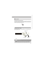
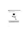
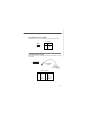
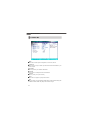
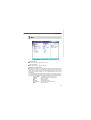
Fuzzy 945GME3
MS-9642 (V3.X) Mainboard
G52-96421X4
i
PDF created with pdfFactory Pro trial version www.pdffactory.com
Copyright Notice
Th e material in this d ocument is the in tellectual p rop erty of MICRO-STAR
INTERNATIONAL. We take every care in the preparation of this document, but no
guarantee is given as to the correctness of its contents. Our products are under
continual improvement and we reserve the right to make changes without notice.
Trademarks
All trademarks are the properties of their respective owners.
Intel® and Pentium® are registered trademarks of Intel Corporation.
AMD, Athlon™, Athlon™ XP, Thoroughbred™, and Duron™ are registered trademarks of AMD Corporation.
NVIDIA, the NVIDIA logo, DualNet, and nForce are registered trademarks or trademarks of NVIDIA Corporation in the United States and/or other countries.
PS/2 and OS ®/2 are registered trademarks of International Business Machines
Corporation.
Windows® 98/2000/NT/XP/Vista are registered trademarks of Microsoft Corporation.
Netware® is a registered trademark of Novell, Inc.
Award® is a registered trademark of Phoenix Technologies Ltd.
AMI® is a registered trademark of American Megatrends Inc.
Revision History
Revision
V3.2
Revision History
Updating LVDS
Date
September 2008
Technical Support
If a problem arises with your system and no solution can be obtained from the user’s
manual, please contact your place of purchase or local distributor. Alternatively,
please try the following help resources for further guidance.
Visit th e MSI web site at http://global.msi.com.tw/index.php?
func=service for FAQ, technical guide, BIOS updates, driver updates, and
other information.
Contact our technical staff at http://ocss.msi.com.tw.
ii
PDF created with pdfFactory Pro trial version www.pdffactory.com
Safety Instructions
1.
Always read the safety instructions carefully.
2.
Keep this User’s Manual for future reference.
3.
Keep this equipment away from humidity.
4.
Lay this equipment on a reliable flat surface before setting it up.
5.
The openings on the enclosure are for air convection hence protects the equipment from overheating. DO NOT COVER THE OPENINGS.
6.
Make sure the voltage of the power source and adjust properly 110/220V before connecting the equipment to the power inlet.
7.
Place the power cord such a way that people can not step on it. Do not place
anything over the power cord.
8.
Always Unplug the Power Cord before inserting any add-on card or module.
9.
All cautions and warnings on the equipment should be noted.
10. Never pour any liquid into the opening that could damage or cause electrical
shock.
11. If any of the following situations arises, get the equipment checked by service
personnel:
The power cord or plug is damaged.
Liquid has penetrated into the equipment.
The equipment has been exposed to moisture.
The equipment does not work well or you can not get it work according to
User’s Manual.
The equipment has dropped and damaged.
The equipment has obvious sign of breakage.
12. DO NOT LEAVE THIS EQUIPMENT IN AN ENVIRONMENT UNCONDITIONED, STORAGE TEMPERATURE ABOVE 600 C (1400F), IT MAY DAMAGE THE EQUIPMENT.
CAUTION: Danger of explosion if battery is incorrectly replaced.
Replace only with the same or equivalent type recommended by
the manufacturer.
iii
FCC-B Radio Frequency Interference Statement
Th is eq u ip men t h as been
tested and found to comply
with the limits for a Class B
digital device, pursuant to Part
15 of the FCC Rules. These limits are designed to provide reasonable protection
against harmful interference in a residential installation. This equipment generates,
uses and can radiate radio frequency energy and, if not installed and used in accordance with the instructions, may cause harmful interference to radio communications.
However, there is no guarantee that interference will not occur in a particular
installation. If this equipment does cause harmful interference to radio or television
reception, which can be determined by turning the equipment off and on, the user is
encouraged to try to correct the interference by one or more of the measures listed
bel ow.
Reorient or relocate the receiving antenna.
Increase the separation between the equipment and receiver.
Connect the equipment into an outlet on a circuit different from that to
which the receiver is connected.
Consult the dealer or an experienced radio/television technician for help.
Notice 1
The changes or modifications not expressly approved by the party responsible for
compliance could void the user’s authority to operate the equipment.
Notice 2
Shielded interface cables and A.C. power cord, if any, must be used in order to
comply with the emission limits.
VOIR LA NOTICE D’INSTALLATION AVANT DE RACCORDER AU RESEAU.
Micro-Star International
MS-9642
This device complies with Part 15 of the FCC Rules. Operation is subject to the
following two conditions:
(1) this device may not cause harmful interference, and
(2) this device must accept any interference received, including interference that
may cause undesired operation.
iv
WEEE (Waste Electrical and Electronic Equipment) Statement
v
vi
vii
CONTENTS
Copyright Notice ..................................................................................................... ii
Trademarks ............................................................................................................ ii
Revision History ..................................................................................................... ii
Technical Support .................................................................................................. ii
Safety Instructions ................................................................................................. iii
FCC-B Radio Frequency Interference Statement ................................................... iv
WEEE (Waste Electrical and Electronic Equipment) Statement ................................ v
Chapter 1 Getting Started .............................................................................. 1-1
Mainboard Specifications ............................................................................. 1-2
Block Diagram ............................................................................................... 1-4
Mainboard Layout ........................................................................................ 1-5
Board Dimension .......................................................................................... 1-6
Back Panel & I/O Shield Drawing .................................................................. 1-7
Power Consumption .................................................................................... 1-8
Safety Compliance & MTBF .......................................................................... 1-9
Chapter 2 Hardware Setup ............................................................................. 2-1
Quick Components Guide ............................................................................. 2-2
CPU (Central Processing Unit) ...................................................................... 2-3
Memory ....................................................................................................... 2-6
Power Supply .............................................................................................. 2-7
Back Panel ................................................................................................... 2-8
Connector .................................................................................................... 2-9
Jumper ...................................................................................................... 2-17
Slot ............................................................................................................ 2-18
Chapter 3 BIOS Setup ...................................................................................... 3-1
Entering Setup ............................................................................................. 3-2
The Menu Bar .............................................................................................. 3-4
Main ............................................................................................................. 3-5
Advanced .................................................................................................... 3-7
PC Health ................................................................................................... 3-17
Security ..................................................................................................... 3-19
System ...................................................................................................... 3-20
Boot ........................................................................................................... 3-21
Exit ............................................................................................................ 3-22
Chapter 4 System Resources ....................................................................... 4-1
Watch Dog Timer Setting .............................................................................. 4-2
Award POST Code ...................................................................................... 4-4
Check Point & Beep Code List .................................................................... 4-10
Resource List ............................................................................................ 4-17
viii
Getting Started
Chapter 1
Getting Started
Thank you for choosing the Fuzzy 945GME3 (MS-9642
v3.X) Mini ITX mainboard from MSI.
Based on the innovative Intel ® 945GM/945GME &
ICH7M controllers for optimal system efficiency, the
Fuzzy 945GME3 accommodates the latest Intel® Core
2 Duo/ Core Duo/ Core Solo/ Celeron M/ Celeron
LV 423 BGA (with BGA Passive Cooler) processors in
Socket M and supports one 240-pin 533/667MHz DDR2
DIMM slot to provide the maximum of 2GB memory
capacity.
In the entry-level and mid-range market segment, the
Fuzzy 945GME3 can provide a high-performance solution for tod ay’s fron t-en d an d g en eral p u rpose
workstation, as well as in the future.
1-1
MS-9642 Mainboard
Mainboard Specifications
Processor
- Intel® Co re 2 Duo/Co re Duo /Core Solo/Celero n M/Celeron LV
423 BGA (with BGA Passive Cooler) CPU in Socket M
- Supports 3 pin CPU Fan Pin-Header with Fan Speed Control
- Supports Intel Dual Core Technology to 533/667MHz and up
Chipset
- North Bridge: Intel® 945GM/ 945GME chipset
- South Bridge: Intel® ICH7M chipset
M e mo ry
- DDR2 533/667 SDRAM (2GB Max)
- 1 DDR2 DIMM slot (240pin / 1.8V)
LAN
- Supports 2 PCI Express Gb Ethernet by Intel® 82573L
Audio
- HDA Codec by Realtek® ALC888 7.1 channel
- Compliant with Azalia 1.0 S pec.
- 6 watt amplif ier (optional)
IDE
- 1 IDE port by ICH7M
- Supports Ultra DMA 66/100 mode
- Supports PIO, Bus Master operation mode
SATA
- SATA ports by ICH7M
- Supports two SATA devices
- Supports storage and data transfers at up to 150MB/s
1-2
Getting Started
Connectors
Back Panel
- 2 RJ-45 LAN jacks
- 2 USB 2.0 ports
- 1 D-Sub VGA connector
- 1 serial port
- 1 PS/2 keyboard port and 1 PS/2 mouse port
- 1 line-in, line-out and mic-in stacked audio jack
Onboard Pinheaders
- 1 USB 2.0 pinheader (2 ports)
- 1 parallel port pinheader
- 1 f ront audio pinheader
- 1 LVDS connector
- 1 Digital I/O pinheader (16 GPIO)
- 4 RS232 pinheaders as COM1~COM4 (optional)
- 1 front panel pinheader
Slots
- 1 PCI Express x16 slot (supports MS-V004 ADD2 DVI Card)
- 1 32-bit/33MHz PCI slot
Form Factor
- Mini ITX
Mounting
- 4 mounting ho les
Environmental
Storage Temperature
- Temperature: -10 oC ~ 70 o C
- Humidity: 10% RH ~ 80% RH
Operation Temperature
- Temperature: 0 oC ~ 60 o C
- Humidity: 80% RH
1-3
MS-9642 Mainboard
Block Diagram
1-4
Getting Started
Mainboard Layout
S ATA 1
ATX1
IDE1
S ATA 2
Top: Serial Port
Bottom: VGA Port
BATT
+
JLPT1
F_US B 2
CP UFA N 1
Intel
ICH7M
J8
Top: Mouse
Bottom: Keyboard
J1
CLR_CMOS1
JFP 1
USB Ports
L AN Chip
JLVDS1
LAN Jacks
Intel
945GM/945GM E
L AN C hip
T: Line- In
M: Line-Out
B: M ic-In
DIMM1
Audio
Codec
JC I1
BIOS
J3
PCI-E1
SY S FAN 2
COM4 COM3
JA MP1 J6
J5
J7
PCI1
COM1 CO M2
SYSFAN1
J4
JAUD1
Fuzzy 945GME3 (MS-9642 v3.X) Mini ITX Mainboard
1-5
MS-9642 Mainboard
Board Dimension
1-6
Getting Started
Back Panel & I/O Shield Drawing
1-7
MS-9642 Mainboard
Power Consumption
Component
Description
Motherboard
CPU
Memory
HDD
Operating system
MS-9642
Intel Core 2 T7200
DDR2 1GB
HITACHI 20G 1.8"
Windows XP Professional SP2
3D Maker 2006
CPU Stress
Enter DOS
Enter BIOS
Idle Mode
S1
S3
S4
S5
1-8
12V
2.17
2.35
1.57
1.63
5V
2.77
2.32
1.62
1.77
3.3V
0.71
0.68
0.66
0.64
-12V
0.054
0.035
0.048
0.048
5Vsb
0.066
0.066
0.055
0.055
0.65
0.92
0
0
0
1.63
1.11
0
0
0
0.69
0.47
0
0
0
0.056
0.05
0
0
0
0.05
0.056
0.33
0.18
0.19
Power (W )
43.211
42.794
29.969
31.373
19.149
19.021
1.65
0.9
0.95
Getting Started
Safety Compliance & MTBF
Standard number
Certification
CE
BSMI
CNS 13438 乙類(1997年版)
C-Tick
AS/NZS CISPR 22:2004
FCC
VCCI
Title of standard
EN 55022:1998+A1:2000+A2:2003 Class B Product family standard
Limits for harmonic current
EN 6100-3-2:2000 Class D
emission
RFI
Limitation of voltage
EN 6100-3-3:1995+A1:2001
fluctuation and flicker in lowvoltage supply system
Immunity EN 55024:1998+A1:2001+A2:2003
Product family standard
FCC CFR Title 47 Part 15 Subpart B: 2005 Class B
CISPR 22: 2005
VCCI V-3:2004, Class B
VCCI V-4:2004, Class B
MTBF - Reliability Prediction
Calculation Model
Operation
Operation
Temperature(°C)
Environment
40
Ground Benign,
Duty Cycle
MTBF(hr.)
6,116.549285
163,491
GB, GC Telcordia Issue 1
Controlled
1-9
MS-9642 Mainboard
1-10
Hardware Setup
Chapter 2
Hardware Setup
This chapter provides you with the information about
hardware setup procedures. While doing the installation,
be careful in holding the components and follow the
installation procedures. For some components, if you
install in the wrong orientation, the components will not
work properly.
Use a grounded wrist strap before handling computer
comp onen ts. Static el ectricity may damag e th e
components.
2-1
MS-9642 Mainboard
Quick Components Guide
JLPT1, p.2-15
ATX1, p.2-7
CPU, p.2-3
IDE1, F_USB2, p.2-14
p.2-9
SATA1/2, p.2-10
CPUFAN1,
p.2-12
JFP1, p.2-12
Back Panel
I/O, p.2-8
J1, p.2-17
CLR_CMOS1, p.2-17
JLVDS1, p.2-16
DIMM Slot,
p.2-6
PCI-E Slot,p.2-18
JCI1,p.2-9
J3, p.2-15
SYSFAN1,
p.2-12
PCI Slot, p.2-18
JAUD1, p.2-11
J6/J5/J7, p.2-17
JAMP1, p.2-11
2-2
J4, p.2-17 SYSFAN2,
p.2-12
COM1~4, p.2-13
Hardware Setup
CPU (Central Processing Unit)
The mainboard supports Intel ® Core 2 Duo/ Core Duo/ Core Solo/ Celeron M/
Celeron LV 423 BGA (with BGA Passive Cooler) processors in Socket M. When you
are installing the CPU, make sure the CPU has a heat sink and a cooling fan
attached on the top to prevent overheating. If you do not have the heat sink and
cooling fan, contact your dealer to purchase and install them before turning on the
computer.
Important
1. Overheating will seriously damage the CPU and system. Always make
sure the cooling fan can work properly to protect the CPU from overheating.
2. Make sure that you apply an even layer of heat sink paste (or thermal tape)
between the CPU and the heatsink to enhance heat dissipation.
3. While replacing the CPU, always turn off the power supply or unplug the
power supply’s power cord from the grounded outlet first to ensure the
safety of CPU.
2-3
MS-9642 Mainboard
CPU & Cooler Set Installation
1. Place the CPU on top of the socket. Make sure to align the gold arrow on the CPU
with the arrow key on the socket.
2. Push the CPU down until its pins securely fit into the socket.
3. On the front end of the CPU socket is a
locking mechanism designed into the
form of a screw. Make sure that you
actuate or deactuate this mechanism
with a screwdriver before and after installing the CPU.
4. Release the metal clips on the retention
mechanism.
Important
Mainboard photos shown in this section are for demonstration only and may
di ffer from the actual look of your
mainboard.
2-4
Hardware Setup
5. Mount the cooler set (fan & heatsink
bundled) on top of the CPU and fit it into
the retention mechanism.
6. Secure the metal clips back to the
retention mechanism.
7. Connect the fan power cable from the
mounted fan to the 3-pin fan power connector on the mainboard.
2-5
MS-9642 Mainboard
Memory
The DIMM slots are intended for system memory modules.
DDR2
240-pin, 1.8V
64x2=128 pin
56x2=112 pin
Installing Memory Modules
1. The memory module has only one notch on the center and will only fit in the right
orientation.
2. Insert the memory module vertically into the DIMM slot. Then push it in until the
golden finger on the memory module is deeply inserted in the DIMM slot.
Important
You can barely see the golden finger if the memory module is properly inserted
in the DIMM slot.
3. The plastic clip at each side of the DIMM slot will automatically close.
Volt
2-6
Notch
Hardware Setup
Power Supply
ATX 20-Pin System Power Connector: ATX1
This connector allows you to connect to an ATX power supply. To connect to the ATX
power supply, make sure the plug of the power supply is inserted in the proper
orientation and the pins are aligned. Then push down the power supply firmly into the
connector.
ATX1
20
11
1
10
ATX1 Pin Definition
PIN
SIGNAL
PIN
SIGNAL
1
2
3
4
5
6
7
8
9
3.3V
3.3V
GND
5V
GND
5V
GND
PW_OK
5V_SB
10
12V
11
12
13
14
15
16
17
18
19
20
3.3V
-12V
GND
PS_ON
GND
GND
GND
-5V
5V
5V
Important
Power supply of 350watts (and above) is highly recommended for system
stability.
2-7
MS-9642 Mainboard
Back Panel
Serial Port
M ouse
Line-In
Line-Out
Mic-In
VGA Port
Keyboard USB Ports
LAN
Serial Port
The serial port is a 16550A high speed communications port that sends/ receives 16
bytes FIFOs. You can attach a serial mouse or other serial devices directly to the
connector.
VGA Port
The DB15-pin female connector is provided for monitor.
Mouse/Keyboard
The standard PS/2® mouse/keyboard DIN connector is for a PS/2® mouse/keyboard.
USB Port
The USB (Universal Serial Bus) port is for attaching USB devices such as keyboard,
mouse, or other USB-compatible devices.
Audio Port
These audio connectors are used for audio devices. You can differentiate the color
of the audio jacks for different audio sound effects.
Line-In (Blue) - Line In / Side-Surround Out in 7.1 channel mode, is used
for extern al CD player, tap epl ayer or oth er aud io
devices.
Line-Out (Green) - Line Out, is a connector for speakers or headphones.
Mic (Pink) - Mic, is a connector for microphones.
LAN
The standard RJ-45 LAN jack is for connection to the Local Area Network (LAN).
You can connect a network cable to it.
LED
Color
LED State
Off
Left
Green
On (steady state)
Activity Indicator
Link Indicator
Condition
LAN link is not established.
LAN link is established.
On (brighter & pulsing) The computer is communicating with another computer on the LAN.
Green
Off
10 Mbit/sec data rate is selected.
On
100 Mbit/sec data rate is selected.
Orange
On
1000 Mbit/sec data rate is selected.
Right
2-8
Hardware Setup
Connector
Chassis Intrusion Connector: JCI1
This connector connects to the chassis intrusion switch cable. If the chassis is
opened, the chassis intrusion mechanism will be activated. The system will record
this status and show a warning message on the screen. To clear the warning, you
must enter the BIOS utility and clear the record.
CHASSIS
GND
1
2
JCI1
44-Pin IDE Connector: IDE1
This 44-pin IDE connector connects to an optional converter that enables connection
to one 44-pin IDE device and one 40-pin IDE device, such as hard disk drives, CDROM and other IDE devices.
Connect to 44-pin
IDE device
IDE1
Connect to IDE1
Connect to 40-pin
IDE device
Important
If you install two IDE devices on the same cable, you must configure the drives
separately to master / slave mode by setting jumpers. Refer to IDE device’s
documentation supplied by the vendors for jumper setting instructions.
2-9
MS-9642 Mainboard
Serial ATA Connector: SATA1, SATA2
This connector is a high-speed Serial ATA interface port. Each connector can connect
one SATA device.
SATA1
SATA2
Important
Please do not fold the Serial ATA cable into 90-degree angle. Otherwise,
data loss may occur during transmission.
2-10
Hardware Setup
Audio Amplifier Connector: JAMP1
The JAMP1 is used to connect audio amplifiers to enhance audio performance.
Pin Definition
JAMP1
1
PIN
SIGNAL
1
AMP_L-
2
3
4
AMP_L+
AMP_RAMP_R+
Front Audio Connector: JAUD1
The JAUD1 connects to an optional audio bracket that provides extra front panel
audio IO jacks.
14
13
2
1
Audio Bracket
(Optional)
JAUD1
JAUD1 Pin Definition
PIN
SIGNAL
PIN
SIGNAL
1
5V_SB
2
VCC3
3
5
7
9
11
13
SPDF0
GND
LEF_OUT
CEN_OUT
AUD_GPIO21
SIDE_L
4
6
8
10
12
14
NA
SPDF1
SURR_OUT_R
SURR_OUT_L
AUDIO GND
SIDE_R
2-11
MS-9642 Mainboard
Fan Power Connector: CPUFAN1, SYSFAN1, SYSFAN2
The fan power connectors support system cooling fan with +12V. When connecting
the wire to the connectors, always note that the red wire is the positive and should
be connected to the +12V; the black wire is Ground and should be connected to GND.
If the mainboard has a System Hardware Monitor chipset onboard, you must use a
specially designed fan with speed sensor to take advantage of the CPU fan control.
SENSOR
+1 2V
GND
SENSOR
+1 2V
GND
SYSFAN1
CPUFAN1
SENSOR
+1 2V
GND
SYSFAN2
Important
Please refer to the recommended CPU fans at Intel® official website or consult
the vendors for proper CPU cooling fan.
Front Panel Connector: JFP1
The mainboard provides one front panel connector for electrical connection to the
front panel switches and LEDs. The JFP1 is compliant with Intel® Front Panel I/O
Connectivity Design Guide.
JFP1
10
Power Switch +
Power
LED
2
9
1
+ Reset
- Switch
- HDD
+ LED
JFP1 Pin Definition
2-12
PIN
SIGNAL
DESCRIPTION
1
2
3
4
5
6
7
8
9
HD_LED +
FP PWR/SLP
HD_LED FP PWR/SLP
RST_SW PWR_SW +
RST_SW +
PWR_SW RSVD_DNU
Hard disk LED pull-up
MSG LED pull-up
Hard disk active LED
MSG LED pull-up
Reset Switch low reference pull-down to GND
Power Switch high reference pull-up
Reset Switch high reference pull-up
Power Switch low reference pull-down to GND
Reserved. Do not use.
Hardware Setup
Serial Port Connector: COM1, COM2, COM3, COM4
This connector is a 16550A high speed communications port that sends/receives 16
bytes FIFOs. You can attach a serial device to it through the optional serial port
bracket.
Pin Definition
PIN
2
1
10
9
COM1/2/3/4
1
2
3
4
5
6
7
8
9
SIGNAL
DESCRIPTION
DCD
SIN
SOUT
DTR
GND
DSR
RTS
CTS
VCC_COM3
Data Carry Detect
Serial In or Receive Data
Serial Out or Transmit Data
Data Terminal Ready
Ground
Data Set Ready
Request To Send
Clear To Send
Power Source
COM4
COM3
COM1
COM2
Voltage Select Serial Port
Serial Port
Voltage Select
J6
(page 2-17) COM4
COM3
J7
(page 2-17)
J4
(page 2-17) COM1
COM2
J5
(page 2-17)
2-13
MS-9642 Mainboard
Front USB Connector: F_USB2
The mainboard provides one USB 2.0 pinheader (optional USB 2.0 bracket available)
that is compliant with Intel® I/O Connectivity Design Guide. USB 2.0 technology increases data transfer rate up to a maximum throughput of 480Mbps, which is 40
times faster than USB 1.1, and is ideal for connecting high-speed USB interface
peripherals such as USB HDD, digital cameras, MP3 players, printers, modems and the like.
F_USB2
2
1
10
9
Pin Definition
PIN
SIGNAL
PIN
SIGNAL
1
VCC
2
VCC
3
USB0-
4
USB1-
5
USB0+
6
USB1+
7
GND
8
GND
9
Key (no pin)
10
USBOC
USB 2.0 Bracket
(Optional)
Important
Note that the pins of VCC and GND must be connected correctly to avoid
possible damage.
2-14
Hardware Setup
Digital IO Connector: J3
The J3 connects to the General-Purpose Input/Output (GPIO) peripheral module.
J3 Pin Definition
J3
19
20
1
2
PIN
SIGNAL
PIN
SIGNAL
1
3
5
7
9
11
13
15
17
19
VCC3
N_GPIO10
N_GPIO11
N_GPIO12
N_GPIO13
N_GPIO14
N_GPIO15
N_GPIO16
N_GPIO17
GND
2
4
6
8
10
12
14
16
18
20
VCC5
N_GPIO20
N_GPIO21
N_GPIO22
N_GPIO23
N_GPIO24
N_GPIO25
N_GPIO26
N_GPIO27
NC
Parallel Port Header: JLPT1
The mainboard provides a 26-pin header for connection to an optional parallel port
bracket. The parallel port is a standard printer port that supports Enhanced Parallel
Port (EPP) and Extended Capabilities Parallel Port (ECP) mode.
Parallel Port
Bracket (Optional)
JLPT1
2
1
26
25
Pin
Signal Name
Pin
Signal Name
1
RSTB#
2
AFD#
3
PRND0
4
ERR#
5
PRND1
6
PINIT#
7
PRND2
8
LPT_SLIN#
9
PRND3
10
GND
11
PRND4
12
GND
13
PRND5
14
GND
15
PRND6
16
GND
17
PRND7
18
GND
19
ACK#
20
GND
21
BUSY
22
GND
23
PE
24
GND
25
SLCT
26
GND
2-15
MS-9642 Mainboard
LVDS Flat Panel Connector: JLVDS1
The LVDS (Low Voltage Differential Signal) connector provides a digital interface
typically used with flat panels. After connecting an LVDS interfaced flat panel to the
JLVDS1, be sure to check the panel datasheet and set the J1 LVDS Power Selection
Jumper to a proper voltage.
SIGNAL
2
40
SIGNAL
2
1
+12V
+12V
4
3
+12V
GND
6
5
+12V
GND
8
7
+3V
LCDVCC
10
9
LCDVCC
1
39
PIN
+12V
JLVDS1
DDC DATA
12
11
DDC CLK
VDD ENABLE
14
13
BKLTCTL
GND
16
15
BKLTEN
LVDS A0+
18
17
LVDS A0-
LVDS A1+
20
19
LVDS A1-
LVDS A2+
22
21
LVDS A2-
LVDS ACLK+
24
23
LVDS ACLK-
LVDS A3+
26
25
LVDS A3-
GND
28
27
GND
LVDS B0+
30
29
LVDS B0-
LVDS B1+
32
31
LVDS B1-
LVDS B2+
34
33
LVDS B2-
LVDS BCLK+
36
35
LVDS BCLK-
LVDS B3+
38
37
LVDS B3-
GND
40
39
GND
After hardware installation is done,
select the LVDS panel type and tune
the LVDS backl ight in the BIOS
Setup Utility.
2-16
PDF created with pdfFactory Pro trial version www.pdffactory.com
Hardware Setup
Jumper
LVDS Power Selection Jumper: J1
Use this jumper to specify the LVDS power.
1
J1
Pin
Signal Name
1
VCC3
2
LCD_SRC (default VCC3)
3
VCC5
Serial Port Power Jumper: J4, J5, J6, J7
These jumpers specify the operation voltage of the onboard serial ports.
1
1
1
3
J4
3
+12V
+5V
1
3
1
J5/J6/J7
+5V
3
1
+12V
Clear CMOS Jumper: CLR_CMOS1
There is a CMOS RAM onboard that has a power supply from external battery to keep
the data of system configuration. With the CMOS RAM, the system can automatically
boot OS every time it is turned on. If you want to clear the system configuration, set
this jumper to clear data.
1
1
1
3
CLR_CMOS1
Clear Data
3
Keep Data
Important
You can clear CMOS by shorting 1-2 pin while the system is off. Then return
to 2-3 pin position. Avoid clearing the CMOS while the system is on; it will
damage the mainboard.
2-17
MS-9642 Mainboard
Slot
PCI (Peripheral Component Interconnect) Express Slot
The PCI Express slot supports the PCI Express interface expansion card.
The PCI Express x 16 slot supports up to 4.0 GB/s transfer rate.
PCI Express x16 Slot
PCI (Peripheral Component Interconnect) Slot
The PCI slot supports LAN card, SCSI card, USB card, and other add-on cards that
comply with PCI specifications.
32-bit PCI Slot
PCI Interrupt Request Routing
The IRQ, acronym of interrupt request line and pronounced I-R-Q, are hardware lines
over which devices can send interrupt signals to the microprocessor. The PCI IRQ
pins are typically connected to the PCI bus pins as follows:
32-bit PCI1
Order 1
Order 2
Order 3
Order 4
INT A#
INT B#
INT C#
INT D#
Important
When adding or removing expansion cards, make sure that you unplug the
power supply first. Meanwhile, read the documentation for the expansion card
to configure any necessary hardware or software settings for the expansion
card, such as jumpers, switches or BIOS configuration.
2-18
BIOS Setup
Chapter 3
BIOS Setup
This chapter provides information on the BIOS Setup
program and allows you to configure the system for
optimum use.
You may need to run the Setup program when:
² An error message appears on the screen during the
system booting up, and requests you to run SETUP.
² You want to change the default settings for customized features.
3-1
MS-9642 Mainboard
Entering Setup
Power on the computer and the system will start POST (Power On Self Test) process.
When the message below appears on the screen, press <F1> key to enter Setup.
Press F1 to enter SETUP
If the message disappears before you respond and you still wish to enter Setup,
restart the system by turning it OFF and On or pressing the RESET button. You may
also restart the system by simultaneously pressing <Ctrl>, <Alt>, and <Delete> keys.
Important
1. The items under each BIOS category described in this chapter are under
continuous update for better system performance. Therefore, the description may be slightly different from the latest BIOS and should be held for
reference only.
2. Upon boot-up, the 1st line appearing after the memory count is the BIOS
version. It is usually in the format:
P9642IMS V3.0 111507 where:
1st digit refers to BIOS maker as A = AMI, W = AWARD, and P =
PHOENIX.
2nd - 5th digit refers to the model number.
6th digit refers to the chipset as I = Intel, N = nVidia, and V = VIA.
7th - 8th digit refers to the customer as MS = all standard customers.
V1.0 refers to the BIOS version.
111507 refers to the date this BIOS was released.
3-2
BIOS Setup
Control Keys
<↑>
<↓>
<←>
<→>
<Enter>
<Esc>
<+/PU>
<-/PD>
<F6>
<F7>
<F10>
Move to the previous item
Move to the next item
Move to the item in the left hand
Move to the item in the right hand
Select the item
Jumps to the Exit menu or returns to the main menu from a
submenu
Increase the numeric value or make changes
Decrease the numeric value or make changes
Load Optimized Defaults
Load Fail-Safe Defaults
Save all the CMOS changes and exit
Getting Help
After entering the Setup menu, the first menu you will see is the Main Menu.
Main Menu
The main menu lists the setup functions you can make changes to. You can use the
arrow keys ( ↑↓ ) to select the item. The on-line description of the highlighted setup
function is displayed at the bottom of the screen.
Sub-Menu
If you find a right pointer symbol (as shown in the right view)
appears to the left of certain fields that means a sub-menu can
be launched from this field. A sub-menu contains additional options for a field parameter. You can use arrow keys ( ↑↓ ) to
highlight the field and press <Enter> to call up the sub-menu. Then you can use the
control keys to enter values and move from field to field within a sub-menu. If you
want to return to the main menu, just press the <Esc >.
General Help <F1>
The BIOS setup program provides a General Help screen. You can call up this screen
from any menu by simply pressing <F1>. The Help screen lists the appropriate keys
to use and the possible selections for the highlighted item. Press <Esc> to exit the
Help screen.
3-3
MS-9642 Mainboard
The Menu Bar
Main
Use this menu for basic system configurations, such as time, date etc.
Advanced
Use this menu to set up the items of special enhanced features available on your
system’s chipset.
PC Health
This entry monitors your hardware health status.
Security
Use this menu to set Supervisor and User Passwords.
System
This entry shows your system summary.
Boot
Use this menu to specify the priority of boot devices.
Exit
This menu allows you to load the BIOS default values or factory default settings into
the BIOS and exit the BIOS setup utility with or without changes.
3-4
BIOS Setup
Main
Date (mm:dd:yy)
The date format is <Day>, <Month> <Date> <Year>.
Time (hh:mm:ss)
The time format is <Hour> <Minute> <Second>.
IDE Channel 0/1 Master/Slave
Press PgUp/<+> or PgDn/<-> to select [Manual], [None] or [Auto] type. Note that the
specifications of your drive must match with the drive table. The hard disk will not
work properly if you enter improper information for this category. If your hard disk
drive type is not matched or listed, you can use [Manual] to define your own drive
type manually.
If you select [Manual], related information is asked to be entered to the following
items. Enter the information directly from the keyboard. This information should be
provided in the documentation from your hard disk vendor or the system manufacturer.
Access Mode
Capacity
Cylinder
Head
Precomp
Landing Zone
Sector
The settings are CHS, LBA, Large, Auto.
The formatted size of the storage device.
Number of cylinders.
Number of heads.
Write precompensation.
Cylinder location of the landing zone.
Number of sectors.
3-5
MS-9642 Mainboard
Halt On
The setting determines whether the system will stop if an error is detected at boot.
When the system stops for the errors preset, it will halt on for 15 seconds and then
automatically resume its operation. Available options are:
[All Errors]
[No Errors]
[All, But Keyboard]
The system stops when any error is detected.
The system doesn’t stop for any detected error.
The system doesn’t stop for a keyboard error.
Base/Extended/Total Memory
The three items show the memory status of the system. (Read-only)
3-6
BIOS Setup
Advanced
Advanced BIOS Features
The sub-menu is used to configure chipset features for optimal system performance.
Quick Power On Self Test
Select [Enabled] to reduce the amount of time required to run the power-on self-
3-7
MS-9642 Mainboard
test (POST). A quick POST skips certain steps. We recommend that you normally disable quick POST. Better to find a problem during POST than lose data
during your work.
Boot Up NumLock Status
This setting is to set the Num Lock status when the system is powered on.
Setting to [On] will turn on the Num Lock key when the system is powered on.
Setting to [Off] will allow users to use the arrow keys on the numeric keypad.
Typematic Rate Setting
This item is used to enable or disable the typematic rate setting including Typematic
Rate & Typematic Delay.
Typematic Rate (Chars/Sec)
After Typematic Rate Setting is enabled, this item allows you to set the rate
(characters/second) at which the keys are accelerated.
Typematic Delay (Msec)
This item allows you to select the delay between when the key was first
pressed and when the acceleration begins.
APIC Mode
This field is used to enable or disable the APIC (Advanced Programmable Interrupt Controller). Due to compliance with PC2001 design guide, the system is
able to run in APIC mode. Enabling APIC mode will expand available IRQ resources for the system.
MPS Version Control For OS
This field allows you to select which MPS (Multi-Processor Specification) version to be used for the operating system. You need to select the MPS version
supported by your operating system. To find out which version to use, consult
the vendor of your operating system.
3-8
BIOS Setup
Advanced Chipset Features
The sub-menu is used to configure chipset features for optimal system performance.
DRAM Timing Selectable
Selects whether DRAM timing is controlled by the SPD (Serial Presence Detect)
EEPROM on the DRAM module. Setting to [By SPD] enables DRAM timing to be
determined automatically by BIOS based on the configurations on the SPD.
Selecting [Manual] allows users to configure the following fields manually.
CAS Latency Time
This controls the timing delay (in clock cycles) before SDRAM starts a read
command after receiving it. Smaller clocks increase system performance while
bigger clocks provide more stable system performance.
DRAM RAS# to CAS# Delay
This field allows you to set the number of cycles for a timing delay between the
CAS and RAS strobe signals, used when DRAM is written to, read from or
refreshed. Fast sp eed offers faster performance while slow speed offers
more stable performance.
DRAM RAS# Precharge
This item controls the number of cycles for Row Address Strobe (RAS) to be
allowed to precharge. If insufficient time is allowed for the RAS to accumulate
its charge before DRAM refresh, refresh may be incomplete and DRAM may fail
to retain data. This item applies only when synchronous DRAM is installed in the
system.
Precharge Delay (tRAS)
The field specifies the idle cycles before precharging an idle bank.
3-9
MS-9642 Mainboard
System Memory Frequency
Use this item to configure the clock frequency of the installed DRAMs.
**VGA Setting**
The following items allow you to configure the VGA settings of the system.
PEG/Onchip VGA Control
This setting allows you to select whether to use the onchip graphics processor
or the PCI Express card.
When set to [Onchip VGA], the motherboard boots up using the onboard graphics processor, even when a PCI Express graphics card is installed.
When set to [PEG Port], the motherboard boots up using the PCI Express graphics card, if one is installed. Otherwise, it defaults to the onboard graphics
processor.
When set to [Auto], the BIOS checks to see if a PCI Express graphics card is
installed. If it detects that a PCI Express graphics card is present, the motherboard
boots up using that card. Otherwise, it defaults to the onboard graphics
processor.
On-Chip Frame Buffer Size
The field specifies the size of system memory allocated for video memory.
Boot Display
Use the field to select the type of device you want to use as the display(s) of
the system.
LVDS Panel Type
This setting specifies the resolution of the LVDS panel.
LVDS Backlight Control
This setting controls the brightness level of the LVDS panel backlight.
3-10
BIOS Setup
Integrated Peripherals
Onboard Device
USB Controller
This setting is used to enable/disable the onboard USB controller.
USB 2.0 Controller
This setting is used to enable/disable the onboard USB 2.0 controller.
USB Keyboard/Mouse Support
Set to [Enabled] if your need to use a USB-interfaced keyboard/mouse in the
3-11
MS-9642 Mainboard
operating system that does not support or have any USB driver installed,
such as DOS and SCO Unix.
Azalia/AC97 Audio Select
Azalia is the codename of “High Definition Audio.” This setting controls the
High Definition Audio interface integrated in the Southbridge.
Audio Amplifier Control
This setting disables/enables the audio amplifier.
Amplifier dB
When the Audio Amplifier Control is set to [Enabled], users may adjust
the amplifier dB range between the lowest useful output and the largest
useful output level.
Onboard Ethernet #1/ #2
These settings disable/enable the onboard Ethernet controller.
Onboard LAN1/ LAN2 Boot ROM
The items enable or disable the initialization of the onboard LAN Boot ROMs
during bootup. Selecting [Disabled] will speed up the boot process.
3-12
BIOS Setup
Super IO Device
Serial Port Setting
Onboard Serial Port 1 / 2 / 3 / 4 / 5
Select an address for Serial Port 1/2/3/4/5.
Serial Port 1 / 2 / 3 / 4 / 5 Use IRQ
Select a corresponding interrupt for Serial Port 1/2/3/4/5.
3-13
MS-9642 Mainboard
Watch Dog
You can enable the system watch-dog timer, a hardware timer that generates either an NMI or a reset when the software that it monitors does not
respond as expected each time the watch dog polls it.
Watch Dog Timer (Minutes)
Select the watch-dog timer period.
Onboard Parallel Port
There is a built-in parallel port on the on-board Super I/O chipset that provides Standard, ECP, and EPP features. It has the following options:
[Disabled]
[3BC/IRQ7]
Line Printer port 0
[278/IRQ5]
Line Printer port 2
[378/IRQ7]
Line Printer port 1
Parallel Port Mode
[SPP]
Standard Parallel Port
[EPP]
Enhanced Parallel Port
[ECP]
Extended Capability Port
[ECP + EPP]
Extended Capability Port + Enhanced Parallel Port
To operate the onboard parallel port as Standard Parallel Port only, choose
[SPP]. To operate the onboard parallel port in the EPP mode simultaneously,
choose [EPP]. By choosing [ECP], the onboard parallel port will operate in
ECP mode only. Choosing [ECP + EPP] will allow the onboard parallel port to
support both the ECP and EPP modes simultaneously.
EPP Mode Select
The onboard parallel port is EPP Spec. compliant, so after the user chooses
the onboard parallel port with the EPP function, the following message will
be displayed on the screen: “EPP Mode Select.” At this time either [EPP 1.7]
spec or [EPP 1.9] spec can be chosen.
ECP Mode Use DMA
The ECP mode has to use the DMA channel, so choose the onboard parallel
port with the ECP feature. After selecting it, the following message will
appear: “ECP Mode Use DMA.” At this time, the user can choose between
DMA channel [3] or [1].
Chassis Intrusion Detect
The field enables or disables the feature of recording the chassis intrusion
status and issuing a warning message if the chassis is once opened. To
clear the warning message, set the field to [Reset]. The setting of the field
will automatically return to [Enabled] later.
3-14
BIOS Setup
Power Management Setup
ACPI Function
This item is to activate the ACPI (Advanced Configuration and Power Management Interface) Function. If your operating system is ACPI-aware, such as
Windows 98SE/2000/ME, select [Enabled].
ACPI Suspend Type
This item specifies the power saving modes for ACPI function. If your operating
system supports ACPI, such as Windows 98SE, Windows ME and Windows
2000, you can choose to enter the Standby mode in S1 (POS) or S3 (STR)
fashion through the setting of this field. Options are:
[S1(POS)] The S1 sleep mode is a low power state. In this state,
no system context is lost (CPU or chipset) and hardware maintains all system context.
[S3(STR)] The S3 sleep mode is a lower power state where the
information of system configuration and open applications/files is saved to main memory that remains
powered while most other hardware components turn
off to save energy. The information stored in memory
will be used to restore the system when a “wake up”
event occurs.
Soft-Off by PWR-BTTN
N
This feature allows users to configure the power button function. Settings are:
[Instant-Off]
The power button functions as a normal power-on/-off button.
[Delay 4 Sec.] When you press the power button, the computer enters the
suspend/sleep mode, but if the button is pressed for more
than four seconds, the computer is turned off.
3-15
MS-9642 Mainboard
USB KB Wake-Up from S3
This setting allows you to enter “Any Key” (max. 8 numbers) to wake up the
system from S3 state.
Resume By Alarm
When [Enabled], your can set the date and time at which the RTC (real-time
clock) alarm awakens the system from suspend mode.
Date (of Month) Alarm
When Resume By Alarm is set to [Enabled], the field specifies the month
for Resume By Alarm.
Time (hh:mm:ss) Alarm
You can choose what hour, minute and second the system will boot up.
PWRON After PWR-Fail
This item specifies whether your system will reboot after a power failure or
interrupt occurs. Available settings are:
[Off]
Leaves the computer in the power off state.
[On]
Leaves the computer in the power on state.
[Former-sts] Restores the system to the status before power failure or interrupt occurred.
3-16
BIOS Setup
PC Health
Smart Fan Setting
Smart System Fan Temp., Smart CPU Fan Temp., Smart Fan3
Temper ature
Select a temperature setting here, and if the temperature of the CPU/system
3-17
MS-9642 Mainboard
climbs up to the selected temperature setting, the system will automatically
increase the speed of the CPU fan/ system fan/ fan3 to cool down the overheated CPU/system.
System Temp Tolerance, CPU Temp Tolerance, Fan3 Tolerance Value
You can select a specific range of the fan tolerance value here for the above
settings. If the current temperatures of the fans reach the maximum threshold
(the temperatures set in previous settings plus the tolerance values you set
here), the fans will speed up for cooling down. On the contrary if the current
temperatures reach the minimum threshold (the set temperatures minus the
tolerance values), the fans will slow down to keep the temperatures stable.
Current System Temp, Current CPU Temperature, System Fan Speed,
CPU Fan Speed, CPU Voltage, 12V, 5V, DDRII, VBAT (V), 5VSB (V)
These items display the current status of all of the monitored hardware devices/
components such as CPU voltage, temperatures and all fans’ speeds.
3-18
BIOS Setup
Security
Set Supervisor Password
Supervisor Password controls access to the BIOS Setup utility.
Set User Password
User Password controls access to the system at boot.
Security Option
This specifies the type of BIOS password protection that is implemented. Settings are
described below:
Op ti on
[Setup]
Description
The password prompt appears only when end users try to run
Setup.
[System]
A password prompt appears every time when the computer is
powered on or when end users try to run Setup.
3-19
MS-9642 Mainboard
System
Machine Type/M odel, Processor, Processor Cache Size, Processor
Speed, System Memory Type, Video Controller, BIOS Date, BIOS Version
These items show the hardware specifications of your system. Read only.
3-20
BIOS Setup
Boot
Hard Disk Boot Priority
This setting allows users to set the boot priority of the specified hard disk devices.
First press <Enter> to enter the sub-menu. Then you may use the arrow keys ( ↑↓ )
to select the desired device, then press <+>, <-> or <PageUp>, <PageDown> key to
move it up/down in the priority list.
First / Second / Third Boot Device
The items allow you to set the sequence of boot devices where BIOS attempts to load
the disk operating system.
Boot Other Device
Setting the option to [Enabled] allows the system to try to boot from other device if the
system fails to boot from the first/second/third boot device.
3-21
MS-9642 Mainboard
Exit
Load Fail-Safe Defaults
Use this menu to load the default values set by the BIOS vendor for stable system
performance.
Load Optimized Defaults
Use this menu to load the default values set by the mainboard manufacturer specifically for optimal performance of the mainboard.
Save & Exit Setup
Save changes to CMOS and exit setup.
Exit Without Saving
Abandon all changes and exit setup.
3-22
System Resources
Chapter 4
System Resources
This chapter provides information on the following
system resources:
1. Watch Dog Timer Setting (p.4-2);
2. Award POST Code (p.4-4);
3. Check Point & Beep Code List (p.4-10);
4. Resource List (p.4-17).
4-1
MS-9642 Mainboard
Watch Dog Timer Setting
ifdef Superio_Support_Watch_Dog
extrn
extrn
mov
call
test
jz
Watch_Dog_Item:near
WD_Timer_Item:near
si,offset MENUITEMGROUP:Watch_Dog_Item
F000_GetItem_Value
al, Watch_Dog_Cmos_bits
@F
;jump if disable
mov dx, 04Eh
mov al, 087h
out dx,al
NEWIODELAY
out dx,al
NEWIODELAY
mov al,07h
mov dx, 04Eh
out dx,al
NEWIODELAY
mov ax,08h
inc dx
out dx,al
NEWIODELAY
;Enter config
;Logical Device 8
mov al, 2Dh
mov dx, 04Eh
out dx,al
NEWIODELAY
inc dx
in
al, dx
and al, 0FEh
out dx,al
NEWIODELAY
mov al, 0F5h
mov dx, 04Eh
out dx,al
NEWIODELAY
mov al,08h
inc dx
out dx,al
NEWIODELAY
4-2
;For By Pass
System Resources
WD_reboot:
mov si,offset MENUITEMGROUP:WD_Timer_Item
call F000_GetItem_Value
mov ah, al
mov al,0F6h
mov dx, 04Eh
out dx,al
NEWIODELAY
;Set time
mov al, ah
inc dx
out dx,al
NEWIODELAY
;fill time 9641_046
mov dx, 04Eh
mov al, 0AAh
out dx, al
NEWIODELAY
;Exit config
@@:
endif ;Superio_Support_Watch_Dog
4-3
MS-9642 Mainboard
Award POST Code
Award BIOS Error Message and Check Point (POST code) List (Need to be
modified, TBD)
• Error/Process Message.
#
Short Name
Description
Possible FRUS
1
CMOS
checksum error
- Defaults
loaded
System board
2
CPU at nnnn
Checksum of CMOS is incorrect, so the
system loads the default equipment
configuration. A checksum error may
indicate that CMOS has become corrupt.
This error may have been caused by a
weak battery. Check the battery and
replace if necessary.
Displays the running speed of the CPU.
3
Press ESC to
skip memory
test
Floppy disk(s)
fail
The user may press Esc to skip the full
memory test.
System board
Cannot find or initialize the floppy drive
controller or the drive. Make sure the
controller is installed correctly. If no floppy
drives are installed, be sure the Diskette
Drive selection in Setup is set to NONE or
AUTO.
Some hard drives require extra time to
initialize.
system board
4
5
6
HARD DISK
initializing
Please wait a
moment
HARD DISK
INSTALL
FAILURE
7
Keyboard error
or no keyboard
present
8
Memory Test:
4-4
processor
System board
Cannot find or initialize the hard drive controller System board
or the drive. Make sure the controller is
installed correctly. If no hard drives are
installed, be sure the Hard Drive selection in
Setup is set to NONE.
Cannot initialize the keyboard. Make sure
the keyboard is attached correctly and no
keys are pressed during POST. To
purposely configure the system without a
keyboard, set the error halt condition in
Setup to HALT ON ALL, BUT KEYBOARD.
The BIOS then ignores the missing
keyboard during POST.
This message displays during a full
memory test, counting down the memory
areas being tested.
System board
DIMM
System board
System Resources
• Check Point List
POST (hex)
CFh
C0h
C1h
A1h
A2h
A3h
A4h
A5h
A6h
A7h
A8h
A9h
AAh
ABh
C3h
C5h
01h
02h
03h
04h
05h
06h
07h
08h
09h
0Ah
0Bh
0Ch
0Dh
0Eh
0Fh
Description
Test CMOS R/W functionality.
Early chipset initialization:
-Disable shadow RAM
-Disable L2 cache (socket 7 or below)
-Program basic chipset registers
Detect memory
-Auto-detection of DRAM size, type and ECC.
-Auto-detection of L2 cache (socket 7 or below)
Set Initial Conditions (Default Values) in EBP
Determine FSB frequency.
Begin Detection of installed DIMMS
Check for Column Latency
200Mhz or 266Mhz
Check for tRAS timing
Check for tRP timing
Check for tRCD timing
Check for ECC Support
Check for refresh timing
Verify that the DIMM's are in matched pairs
Expand compressed BIOS code to DRAM
Call chipset hook to copy BIOS back to E000 & F000 shadow
RAM.
Expand the Xgroup codes locating in physical address 1000:0
Reserved
Initial Superio_Early_Init switch.
Reserved
1. Blank out screen
2. Clear CMOS error flag
Reserved
1. Clear 8042 interface
2. Initialize 8042 self-test
1. Test special keyboard controller for Winbond 977 series Super
I/O chips.
2. Enable keyboard interface.
Reserved
1. Disable PS/2 mouse interface (optional).
2. Auto detect ports for keyboard & mouse followed by a port & interface swap
(optional).
3. Reset keyboard for Winbond 977 series Super I/O chips.
Reserved
Reserved
Reserved
Test F000h segment shadow to see whether it is R/W-able or not. If
test fails, keep beeping the speaker.
Reserved
4-5
MS-9642 Mainboard
10h
11h
12h
13h
14h
15h
16h
17h
18h
19h
1Ah
1Bh
1Ch
1Dh
1Eh
1Fh
20h
21h
22h
23h
24h
25h
26h
27h
28h
29h
4-6
Auto detect flash type to load appropriate flash R/W codes into the
run time area in F000 for ESCD & DMI support.
Reserved
Use walking 1’s algorithm to check out interface in CMOS
circuitry. Also set real-time clock power status, and then check for
override.
Reserved
Program chipset default values into chipset. Chipset default
values are MODBINable by OEM customers.
Reserved
Initial Early_Init_Onboard_Generator switch.
Reserved
Detect CPU information including brand, SMI type (Cyrix or
Intel) and CPU level (586 or 686).
Reserved
Reserved
Initial interrupts vector table. If no special specified, all H/W
interrupts are directed to SPURIOUS_INT_HDLR & S/W
interrupts to SPURIOUS_soft_HDLR.
Reserved
Initial EARLY_PM_INIT switch.
Reserved
Load keyboard matrix (notebook platform)
Reserved
HPM initialization (notebook platform)
Reserved
1. Check validity of RTC value:
e.g. a value of 5Ah is an invalid value for RTC minute.
2. Load CMOS settings into BIOS stack. If CMOS checksum fails, use default
value instead.
3. Prepare BIOS resource map for PCI & PnP use. If ESCD is valid, take into
consideration of the ESCD’s legacy information.
4. Onboard clock generator initialization. Disable respective clock resource to
empty PCI & DIMM slots.
5. Early PCI initialization:
-Enumerate PCI bus number
-Assign memory & I/O resource
-Search for a valid VGA device & VGA BIOS, and put it
into C000:0.
Reserved
Reserved
Reserved
Initialize INT 09 buffer
Reserved
1. Program CPU internal MTRR (P6 & PII) for 0-640K memory address.
2. Initialize the APIC for Pentium class CPU.
3. Program early chipset according to CMOS setup. Example: onboard IDE
controller.
4. Measure CPU speed.
5. Invoke video BIOS.
System Resources
2Ah
2Bh
2Ch
2Dh
2Eh
2Fh
30h
31h
32h
33h
34h
35h
36h
37h
38h
39h
3Ah
3Bh
3Ch
3Dh
3Eh
3Fh
40h
41h
42h
43h
44h
45h
46h
47h
48h
49h
4Ah
4Bh
4Ch
4Dh
4Eh
4Fh
Reserved
Reserved
Reserved
1. Initialize multi-language
2. Put information on screen display, including Award title, CPU type, CPU speed
….
Reserved
Reserved
Reserved
Reserved
Reserved
Reset keyboard except Winbond 977 series Super I/O chips.
Reserved
Reserved
Reserved
Reserved
Reserved
Reserved
Reserved
Reserved
Test 8254
Reserved
Test 8259 interrupt mask bits for channel 1.
Reserved
Test 8259 interrupt mask bits for channel 2.
Reserved
Reserved
Test 8259 functionality.
Reserved
Reserved
Reserved
Initialize EISA slot
Reserved
1. Calculate total memory by testing the last double word of each 64K page.
2. Program write allocation for AMD K5 CPU.
Reserved
Reserved
Reserved
Reserved
1. Program MTRR of M1 CPU
2. Initialize L2 cache for P6 class CPU & program CPU with proper cacheable
range.
3. Initialize the APIC for P6 class CPU.
4. On MP platform, adjust the cacheable range to smaller one in case the
cacheable ranges between each CPU are not identical.
Reserved
4-7
MS-9642 Mainboard
50h
51h
52h
53h
54h
55h
56h
57h
58h
59h
5Ah
5Bh
5Ch
5Dh
5Eh
5Fh
60h
61h
62h
63h
64h
65h
66h
67h
68h
69h
6Ah
6Bh
6Ch
6Dh
6Eh
6Fh
70h
71h
72h
73h
74h
75h
4-8
Initialize USB
Reserved
Test all memory (clear all extended memory to 0)
Reserved
Reserved
Display number of processors (multi-processor platform)
Reserved
1. Display PnP logo
2. Early ISA PnP initialization
-Assign CSN to every ISA PnP device.
Reserved
Initialize the combined Trend Anti-Virus code.
Reserved
(Optional Feature)
Show message for entering AWDFLASH.EXE from FDD (optional)
Reserved
1. Initialize Init_Onboard_Super_IO switch.
2. Initialize Init_Onbaord_AUDIO switch.
Reserved
Reserved
Okay to enter Setup utility; i.e. not until this POST stage can users
enter the CMOS setup utility.
Reserved
Reserved
Reserved
Reserved
Initialize PS/2 Mouse
Reserved
Prepare memory size information for function call:
INT 15h ax=E820h
Reserved
Turn on L2 cache
Reserved
Program chipset registers according to items described in Setup &
Auto-configuration table.
Reserved
1. Assign resources to all ISA PnP devices.
2. Auto assign ports to onboard COM ports if the corresponding item in Setup
is set to “AUTO”.
Reserved
1. Initialize floppy controller
2. Set up floppy related fields in 40:hardware.
Reserved
Reserved
Reserved
(Optional Feature)
Enter AWDFLASH.EXE if :
-AWDFLASH is found in floppy drive.
-ALT+F2 is pressed
Reserved
Detect & install all IDE devices: HDD, LS120, ZIP, CDROM…..
System Resources
76h
77h
78h
79h
7Ah
7Bh
7Ch
7Dh
7Eh
7Fh
80h
81h
82h
83h
84h
85h
86h
87h
88h
89h
90h
91h
92h
93h
94h
95h
96h
FFh
Reserved
Detect serial ports & parallel ports.
Reserved
Reserved
Detect & install co-processor
Reserved
Reserved
Reserved
Reserved
1. Switch back to text mode if full screen logo is supported.
-If errors occur, report errors & wait for keys
-If no errors occur or F1 key is pressed to continue:
wClear EPA or customization logo.
Reserved
Reserved
1. Call chipset power management hook.
2. Recover the text fond used by EPA logo (not for full screen logo)
3. If password is set, ask for password.
Save all data in stack back to CMOS
Initialize ISA PnP boot devices
1. USB final Initialization
2. NET PC: Build SYSID structure
3. Switch screen back to text mode
4. Set up ACPI table at top of memory.
5. Invoke ISA adapter ROMs
6. Assign IRQs to PCI devices
7. Initialize APM
8. Clear noise of IRQs.
Reserved
Reserved
Reserved
Reserved
Reserved
Reserved
Reserved
Read HDD boot sector information for Trend Anti-Virus code
1. Enable L2 cache
2. Program boot up speed
3. Chipset final initialization.
4. Power management final initialization
5. Clear screen & display summary table
6. Program K6 write allocation
7. Program P6 class write combining
1. Program daylight saving
2. Update keyboard LED & typematic rate
1. Build MP table
2. Build & update ESCD
3. Set CMOS century to 20h or 19h
4. Load CMOS time into DOS timer tick
5. Build MSIRQ routing table.
Boot attempt (INT 19h)
4-9
MS-9642 Mainboard
Check Point & Beep Code List
Bootblock Initialization Code Checkpoints
Checkpoint
Description
Before D0
If boot block debugger is enabled, CPU cache-as-RAM functionality is enabled at this
point. Stack will be enabled from this point.
D0
Early Boot Strap Processor (BSP) initialization like microcode update, frequency and
other CPU critical initialization. Early chipset initialization is done.
D1
Early super I/O initialization is done including RTC and keyboard controller. Serial port
is enabled at this point if needed for debugging. NMI is disabled. Perform keyboard
controller BAT test. Save power-on CPUID value in scratch CMOS. Go to flat mode with
4GB limit and GA20 enabled.
D2
Verify the boot block checksum. System will hang here if checksum is bad.
D3
Disable CACHE before memory detection. Execute full memory sizing module. If
memory sizing module not executed, start memory refresh and do memory sizing in
Boot block code. Do additional chipset initialization. Re-enable CACHE. Verify that flat
mode is enabled.
D4
Test base 512KB memory. Adjust policies and cache first 8MB. Set stack.
D5
Bootblock code is copied from ROM to lower system memory and control is given to it.
BIOS now executes out of RAM. Copies compressed boot block code to memory in
right segments. Copies BIOS from ROM to RAM for faster access. Performs main BIOS
checksum and updates recovery status accordingly.
D6
Both key sequence and OEM specific method is checked to determine if BIOS recovery
is forced. If BIOS recovery is necessary, control flows to checkpoint E0. See Bootblock
Recovery Code Checkpoints section of document for more information.
D7
Restore CPUID value back into register. The Bootblock-Runtime interface module is
moved to system memory and control is given to it. Determine whether to execute serial
flash.
D8
The Runtime module is uncompressed into memory. CPUID information is stored in
memory.
D9
Store the Uncompressed pointer for future use in PMM. Copying Main BIOS into
memory. Leaves all RAM below 1MB Read-Write including E000 and F000 shadow
areas but closing SMRAM.
DA
Restore CPUID value back into register. Give control to BIOS POST
(ExecutePOSTKernel). See POST Code Checkpoints section of document for more
information.
DC
System is waking from ACPI S3 state
E1-E8
OEM memory detection/configuration error. This range is reserved for chipset vendors
EC-EE
& system manufacturers. The error associated with this value may be different from one
platform to the next.
4-10
System Resources
Bootblock Recovery Code Checkpoints
Checkpoint
Description
E0
Initialize the floppy controller in the super I/O. Some interrupt vectors are initialized.
DMA controller is initialized. 8259 interrupt controller is initialized. L1 cache is
enabled.
E9
Set up floppy controller and data. Attempt to read from floppy.
EA
Enable ATAPI hardware. Attempt to read from ARMD and ATAPI CDROM.
EB
Disable ATAPI hardware. Jump back to checkpoint E9.
EF
Read error occurred on media. Jump back to checkpoint EB.
F0
Search for pre-defined recovery file name in root directory.
F1
Recovery file not found.
F2
Start reading FAT table and analyze FAT to find the clusters occupied by the recovery
file.
F3
Start reading the recovery file cluster by cluster.
F5
Disable L1 cache.
FA
Check the validity of the recovery file configuration to the current configuration of the
flash part.
FB
Make flash write enabled through chipset and OEM specific method. Detect proper
flash part. Verify that the found flash part size equals the recovery file size.
F4
The recovery file size does not equal the found flash part size.
FC
Erase the flash part.
FD
Program the flash part.
FF
The flash has been updated successfully. Make flash write disabled. Disable ATAPI
hardware. Restore CPUID value back into register. Give control to F000 ROM at
F000:FFF0h.
4-11
MS-9642 Mainboard
POST Code Checkpoints
Checkpoint
Description
03
Disable NMI, Parity, video for EGA, and DMA controllers. Initialize BIOS, POST,
Runtime data area. Also initialize BIOS modules on POST entry and GPNV area.
Initialized CMOS as mentioned in the Kernel Variable "wCMOSFlags."
04
Check CMOS diagnostic byte to determine if battery power is OK and CMOS checksum
is OK. Verify CMOS checksum manually by reading storage area. If the CMOS
checksum is bad, update CMOS with power-on default values and clear passwords.
Initialize status register A.
Initializes data variables that are based on CMOS setup questions. Initializes both the
8259 compatible PICs in the system
05
Initializes the interrupt controlling hardware (generally PIC) and interrupt vector table.
06
Do R/W test to CH-2 count reg. Initialize CH-0 as system timer. Install the POSTINT1Ch
handler. Enable IRQ-0 in PIC for system timer interrupt. Traps INT1Ch vector to
"POSTINT1ChHandlerBlock."
07
Fixes CPU POST interface calling pointer.
08
Initializes the CPU. The BAT test is being done on KBC. Program the keyboard
controller command byte is being done after Auto detection of KB/MS using AMI KB-5.
C0
Early CPU Init Start -- Disable Cache – Init Local APIC
C1
Set up boot strap processor Information
C2
Set up boot strap processor for POST
C5
Enumerate and set up application processors
C6
Re-enable cache for boot strap processor
C7
Early CPU Init Exit
0A
Initializes the 8042 compatible Key Board Controller.
0B
Detects the presence of PS/2 mouse.
0C
Detects the presence of Keyboard in KBC port.
0E
Testing and initialization of different Input Devices. Also, update the Kernel Variables.
Traps the INT09h vector, so that the POST INT09h handler gets control for IRQ1.
Uncompress all available language, BIOS logo, and Silent logo modules.
13
Early POST initialization of chipset registers.
20
Relocate System Management Interrupt vector for all CPU in the system.
24
Uncompress and initialize any platform specific BIOS modules. GPNV is initialized at
this checkpoint.
4-12
System Resources
2A
Initializes different devices through DIM.
See DIM Code Checkpoints section of document for more information.
2C
Initializes different devices. Detects and initializes the video adapter installed in the
system that has optional ROMs.
2E
Initializes all the output devices.
31
Allocate memory for ADM module and uncompress it. Give control to ADM module for
initialization. Initialize language and font modules for ADM. Activate ADM module.
33
Initializes the silent boot module. Set the window for displaying text information.
37
Displaying sign-on message, CPU information, setup key message, and any OEM
specific information.
38
Initializes different devices through DIM. See DIM Code Checkpoints section of
39
Initializes DMAC-1 & DMAC-2.
3A
Initialize RTC date/time.
3B
Test for total memory installed in the system. Also, Check for DEL or ESC keys to limit
document for more information. USB controllers are initialized at this point.
memory test. Display total memory in the system.
3C
40
Mid POST initialization of chipset registers.
Detect different devices (Parallel ports, serial ports, and coprocessor in CPU, … etc.)
successfully installed in the system and update the BDA, EBDA…etc.
52
Updates CMOS memory size from memory found in memory test. Allocates memory for
Extended BIOS Data Area from base memory. Programming the memory hole or any
kind of implementation that needs an adjustment in system RAM size if needed.
60
Initializes NUM-LOCK status and programs the KBD typematic rate.
75
Initialize Int-13 and prepare for IPL detection.
78
Initializes IPL devices controlled by BIOS and option ROMs.
7C
Generate and write contents of ESCD in NVRam.
84
Log errors encountered during POST.
85
Display errors to the user and gets the user response for error.
87
Execute BIOS setup if needed / requested. Check boot password if installed.
8C
Late POST initialization of chipset registers.
8D
Build ACPI tables (if ACPI is supported)
8E
Program the peripheral parameters. Enable/Disable NMI as selected
4-13
MS-9642 Mainboard
90
Initialization of system management interrupts by invoking all handlers. Please note this
checkpoint comes right after checkpoint 20h
A1
Clean-up work needed before booting to OS.
A2
Takes care of runtime image preparation for different BIOS modules. Fill the free area in
F000h segment with 0FFh. Initializes the Microsoft IRQ Routing Table. Prepares the
runtime language module. Disables the system configuration display if needed.
A4
A7
Initialize runtime language module. Display boot option popup menu.
Displays the system configuration screen if enabled. Initialize the CPU’s before boot,
which includes the programming of the MTRR’s.
4-14
A9
Wait for user input at config display if needed.
AA
Uninstall POST INT1Ch vector and INT09h vector.
AB
Prepare BBS for Int 19 boot. Init MP tables.
AC
End of POST initialization of chipset registers. De-initializes the ADM module.
B1
Save system context for ACPI. Prepare CPU for OS boot including final MTRR values.
00
Passes control to OS Loader (typically INT19h).
System Resources
Beep Codes
Boot Block Beep Codes
Number of Beeps
Description
1
Insert diskette in floppy drive A:
2
‘AMIBOOT.ROM’ file not found in root directory of diskette in A:
3
Base Memory error
4
Flash Programming successful
5
Floppy read error
6
Keyboard controller BAT command failed
7
No Flash EPROM detected
8
Floppy controller failure
9
Boot Block BIOS checksum error
10
Flash Erase error
11
Flash Program error
12
‘AMIBOOT.ROM’ file size error
13
BIOS ROM image mismatch (file layout does not match image present in flash
device)
POST BIOS Beep Codes
Number of Beeps
Description
1
Memory refresh timer error.
2
Parity error in base memory (first 64KB block)
3
Base memory read/write test error
4
Motherboard timer not operational
5
Processor error
6
8042 Gate A20 test error (cannot switch to protected mode)
7
General exception error (processor exception interrupt error)
8
Display memory error (system video adapter)
9
AMIBIOS ROM checksum error
10
CMOS shutdown register read/write error
11
Cache memory test failed
4-15
MS-9642 Mainboard
Troubleshooting POST BIOS Beep Codes
Number of Beeps
Troubleshooting Action
1, 2 or 3
Reseat the memory, or replace with known good modules.
4-7, 9-11
Fatal error indicating a serious problem with the system. Consult your system
manufacturer. Before declaring the motherboard beyond all hope, eliminate the
possibility of interference by a malfunctioning add-in card. Remove all expansion
cards except the video adapter.
‧ If beep codes are generated when all other expansion cards are absent, consult
your system manufacturer’s technical support.
‧ If beep codes are not generated when all other expansion cards are absent, one
of the add-in cards is causing the malfunction. Insert the cards back into the
system one at a time until the problem happens again. This will reveal the
malfunctioning card.
8
If the system video adapter is an add-in card, replace or reseat the video adapter.
If the video adapter is an integrated part of the system board, the board may be
faulty.
4-16
System Resources
Resource List
ICH7M GPI/O Definition
Pin
GPIO Type Multi
Power
Conn.
AB18
0
I
BM_BUSY#
VCC3P3
BM_BUSY#
C8
1
I
PCIREQ[5]#
V5REF
PREQ#5#
G8
2
I
PIRQE#
V5REF
PIRQE#
F7
3
I
PIRQF#
V5REF
PIQRF#
F8
4
I
PIRQG#
V5REF
PIRQG#
G7
5
I
PIRQH#
V5REF
PIRQH#
AC21
6
I
NC
VCC3P3
SIO_OVT#
AC18
7
I
NC
VCC3P3
BIOS_WP#
E21
8
I
NC
VCCSUS3P3
VCC3V_SB
E20
9
I
NC
VCCSUS3P3
LAN1_EN
A20
10
I
NC
VCCSUS3P3
LAN2_EN
B23
11
I
SMBALERT#
VCCSUS3P3
SMB ALERT#
F19
12
I
NC
VCCSUS3P3
LAN3_EN
E19
13
I
NC
VCCSUS3P3
SIO_PME#
R4
14
I
NC
VCCSUS3P3
VCC3V_SB
E22
15
O
NC
VCCSUS3P3
AT/ATX SELECT
AC22
16
O
DPRSLPVR
VCC3P3
DPRSLPVR
D8
17
O
PCIGNT5#
VCC3P3
NC
AC20
18
O
STPPCI#
VCC3P3
STP_PCI#
AH18
19
I
SATA1GP
VCC3P3
AMP_GAIN0
AF21
20
O
STPCPU#
VCC3P3
STP_CPU#
AF19
21
I
SATA0GP
VCC3P3
AMP_EN
A13
22
O
REQ4#
VCC3P3
PREQ#4
AA51
23
O
LDRQ1#
VCC3P3
NC
B3
24
O
NC
VCCSUS3P3
NC
D20
25
O
NC
VCCSUS3P3
NC
A21
26
O
EL_RSVD
VCCSUS3P3
NC
B12
27
O
EL_STATE0
VCCSUS3P3
NC
E23
28
O
EL_STATE1
VCCSUS3P3
NC
C3
29
I
OC5#
VCCSUS3P3
VCC3V_SB
A2
30
I
OC6#
VCCSUS3P3
VCC3V_SB
B3
31
I
OC7#
VCCSUS3P3
VCC3V_SB
AG18
32
O
CLKRUN#
VCC3P3
PM_CLKRUN#
4-17
MS-9642 Mainboard
4-18
Pin
GPIO Type Multi
Power
Conn.
AC19
33
O
AZ_DOCK_EN#
VCC3P3
AUXGPIO_DIR1
U2
34
O
AZ_DOCK_RST#
VCC3P3
AUXGPIO_DIR2
AD21
35
O
SATACLKREQ#
VCC3P3
NC
AH19
36
I
SATA2GP
VCC3P3
AMP_GAIN1
AE19
37
I
SATA3GP
VCC3P3
NC
AD20
38
O
NC
VCC3P3
AUXGPIO_OE#
AE20
39
O
NC
VCC3P3
NC
A14
48
O
GNT4#
VCC3P3
NC
AG24
49
OD
H_PWRGD
V_FSB_VTT
H_PWRGD
System Resources
Winbond W83627EHG SIO GPI/O Definition
GPIO
Pin
Typ
Power
Connection
GPIO10
128
IO
VCC
AUXGPIO10
GPIO11
127
IO
VCC
AUXGPIO11
GPIO12
126
IO
VCC
AUXGPIO12
GPIO13
125
O
VCC
AUXGPIO13
GPIO14
124
O
VCC
AUXGPIO14
GPIO15
123
IO
VCC
AUXGPIO15
GPIO16
122
IO
VCC
AUXGPIO16
GPIO17
121
IO
VCC
AUXGPIO17
GPIO20
120
O
VCC
NC
GPIO21
119
I
VCC
AUD_GPIO21
GPIO22
19
IO
VCC
NC
GPIO23
2
IO
VCC
NC
GPIO24
66
IO
VSB
MSDAT#
GPIO25
65
IO
VSB
MSCLK#
GPIO26
63
IO
VSB
KBDAT#
GPIO27
62
IO
VSB
KBCLK#
GPIO30
92
IO
VSB
AUXGPIO20
GPIO31
91
IO
VSB
AUXGPIO21
GPIO32
90
I
VSB
AUXGPIO22
GPIO33
89
IO
VSB
AUXGPIO23
GPIO34
88
IO
VSB
AUXGPIO24
GPIO35
87
IO
VSB
AUXGPIO25
GPIO36
69
IO
VSB
AUXGPIO26
GPIO37
64
IO
VSB
AUXGPIO27
GPIO40
85
IO
VSB
NC
GPIO41
84
IO
VSB
NC
GPIO42
83
IO
VSB
SOUTB
GPIO43
82
IO
VSB
NC
GPIO44
81
IO
VSB
NC
GPIO45
80
IO
VSB
NC
GPIO46
79
IO
VSB
NC
GPIO47
68
IO
VSB
NC
GPIO50
77
IO
VSB
EN_VRM10
GPIO51
75
IO
VSB
NC
4-19
MS-9642 Mainboard
4-20
GPIO
Pin
Typ
Power
Connection
GPIO52
73
I
VSB
SLP_S3#
GPIO53
72
O
VSB
PS_ON#
GPIO54
71
IO
VSB
NC
GPIO55
70
IO
VSB
NC
GPIO56
68
I
VSB
PWRBTIN
GPIO57
67
O
VSB
PWRBTN#
GPIO60
57
IO
VCC
RIA#
GPIO61
56
IO
VCC
DCDA#
GPIO62
54
IO
VCC
SOUTA
GPIO63
53
IO
VCC
SINA
GPIO64
52
IO
VCC
DTRA#
GPIO65
51
IO
VCC
RTSA#
GPIO66
50
IO
VCC
DSRA#
GPIO67
49
IO
VCC
CTSA#
System Resources
I/O Map
I/O Port
0000-000F
0020-0021
0040-0043
004E-004F
0060, 0064
0070-0073
0080-0090
0092
00A0-00A1
00B2-00B3
00C0-00DF
00F0-00FF
01F0-01F7
02F8-02FF
0376
0378-037F
03F6
03F8-03FF
0400-045F
0500-050F
0CF8-0CFF
Description
DMA Controller 1
Interrupt Controller 1
System Timer
SIO Port
Keyboard Controller
RTC and CMOS
DMA Controller Page Registers
Port 92h
Interrupt Controller 2
APM register
DMA Controller 2
Numeric Data Processor
Primary IDE Controller
COM2
Secondary IDE Controller
LPT1
Primary IDE Controller
COM1
ACPI I/O Space
SMBus I/O Space
PCI Configuration Port
4-21
MS-9642 Mainboard
PCI Devices
4-22
System Resources
SMBus Resource Allocation
SMBus Resource Allocation
Device
Address
Description
MS-7
0101 111X MSI ACPI Controller
DIMM Slot 1010 0000 SPD
ISA Interrupt Allocation
IRQ
IRQ0
IRQ1
IRQ2
IRQ3
IRQ4
IRQ5
IRQ6
IRQ7
IRQ8
IRQ9
IRQ10
IRQ11
IRQ12
IRQ13
IRQ14
IRQ15
Description
System Timer
Keyboard Controller
Second 8259A
COM2 / COM4
COM1 / COM3
LPT2
Floppy Disk Drive
LPT1
RTC
Redirected IRQ2
Reserved
Reserved
Reserved
Math Coprocessor
Fixed Disk
Reserved
ISA DMA Channel Allocation
4-23