1
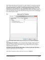
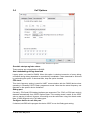
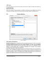
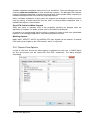
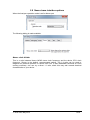
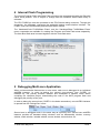
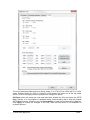
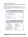
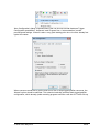
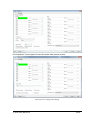
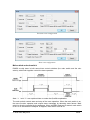
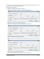
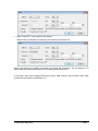
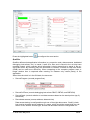
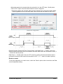
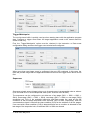
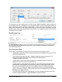
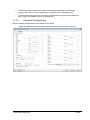
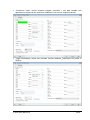
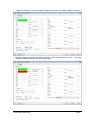
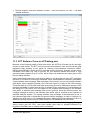
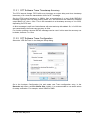
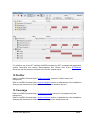
_ V9.12. 225 Technical Notes Renesas RH850 Family On-Chip Emulation This document is intended to be used together with the CPU reference manual provided by the silicon vendor. This document assumes knowledge of the CPU functionality and the terminology and concepts defined and explained in the CPU reference manual. Basic knowledge of winIDEA is also necessary. This document deals with specifics and advanced details and it is not meant as a basic or introductory text. Contents Contents 1 1 Introduction 3 2 Emulation options 2.1 Hardware Options 2.2 Initialization Sequence 2.3 JTAG Scan Speed 4 4 5 5 3 CPU Setup 3.1 Debugging 3.2 Reset 3.3 Advanced SoC Options 3.4 SoC Options 3.5 Device Options 3.5.1 Device Core Options 3.6 Nexus trace interface options 6 6 7 8 9 10 11 12 4 Internal Flash Programming 13 5 Debugging Multi-core Application 13 6 Option Bytes Programming 15 7 Hot Attach 17 8 Real-Time Memory Access 18 9 Access Breakpoints 19 10 Emulation Notes 10.1 Code Execution on Session Startup 10.2 Interrupts 19 19 20 11 Trace 11.1 Trace Concept 11.2 Trace Configuration 11.2.1 Record Everything 11.2.2 OCTB/Nexus Trigger/Qualifier 11.2.3 Example Configurations 11.3 SFT Software Trace via LPD debug port 11.3.1 SFT Software Trace Timestamp Accuracy 11.3.2 SFT Software Trace Configuration 21 21 22 22 23 33 36 37 37 12 Profiler 40 13 Coverage 40 iSYSTEM, May 2015 1/41 14 Getting Started 41 15 Troubleshooting 41 iSYSTEM, May 2015 2/41 1 Introduction On-chip debug support for Renesas RH850 line family is based on the Renesas JTAG Nexus and Low-pin Debug (LPD) debug interface options. Some of the debug functionalities are hard-coded in the on-chip debug module while the others may be implemented by custom monitor functions, loaded in a dedicated CPU memory space and then called by the winIDEA debugger. Debug Features Hardware execution breakpoints Access Breakpoints Real-time access Program & Data Flash Programming Flash Option Bytes programming Security Function Hot Attach iSYSTEM, May 2015 3/41 2 Emulation options 2.1 Hardware Options Emulation options, Hardware pane Debug I/O levels The development system can be configured in a way that the debug BDM signals are driven at 3.3V, 5V or target voltage level (Vref). When Vref Debug I/O level is selected, a voltage from the target debug connector connects to a voltage follower, which then powers debug tool I/O buffers that physically drive the BDM signals. The user must ensure that the target power supply is connected to the Vref pin on the target BDM connector and that the target is powered before the debug session is started. If these two conditions are not meet, the initial debug connection will most likely fail. In some cases it may even succeed, but then the system will behave erratically. Check Vref on startup This option is available for iC5000 development system only. When checked, the system will check the presence of voltage on the Vref pin on the target debug connector. A warning message pops up if no voltage or too low voltage is detected. Hot Attach Option must be checked when Hot Attach is used. Please refer to the Hot Attach chapter for more details on Hot Attach use. Vref option cannot be used in this case, because debugger I/O buffers are not powered until connection to target is made. Hence winIDEA automatically switches to e.g. 5V source from debugger, when the option is checked. Note: Hot Attach function cannot be used for any flash programming or code download! iSYSTEM, May 2015 4/41 2.2 Initialization Sequence Primarily, initialization sequence is used on On-Chip Debug systems to initialize the CPU after reset to be able to download the code to the target (CPU or CPU external) memory. Typically, there is no need to use the initialization sequence in case of the RH850. Initialization sequence may be required on some CPU families when it is required by the application being debugged. The debugger executes initialization immediately after reset and then downloads the code. Detailed information may be found in the Initialization Sequence help topic. 2.3 JTAG Scan Speed JTAG Scan Speed definition Scan speed JTAG Scan Speed is automatically set to the ‘Free’ mode. The free running JTAG clock is required by the RH850 debug interface. The clock frequency is 2 MHz. Note: When using LPD debug interface, please refer to the Advanced Options chapter for setting the LPD clock frequency. iSYSTEM, May 2015 5/41 3 CPU Setup 3.1 Debugging Debugging options dialog Set / clear SW BPs before Run When the option is checked, then a software breakpoint is not set / cleared immediately, but is just remembered. Only when the CPU is set to running are the breakpoints committed. This way several breakpoints can be changed but only one re-FLASH operation takes place. This is particularly noticeable in testIDEA operation with many stubs and also during a regular debugging session when several breakpoints are set / cleared within the same flash erase block. External Oscillator Clock Before performing first debug connection and download, the user must enter a frequency of the external quartz oscillator connected to the target CPU. This value is used by the Renesas native FP5 serial protocol during the CPU flash programming. Ignore access errors Any access to an undefined address space or non-initialized internal RAM returns an error status. This is displayed with question marks ‘?’ all over the memory window when such address base is given. However, check this option to be able to inspect the state of the internal RAM, and uncheck the ‘Initialize internal RAM’ option. iSYSTEM, May 2015 6/41 Initialize internal RAM Per default this option should be set to Auto (FLASH). After reset, the microcontroller internal SRAM is not initialized and cannot be used. When the option is checked, the debugger initializes internal SRAM, which might be required for internal flash programming. Set the option to ‘Never’ only when it’s required to analyze the microcontroller state after a reset. Use case would be to download the code to the flash with this option checked. Next, power off and power on complete system and then perform a debug reset only. At that point internal RAM is intact by the debugger and the microcontroller state can be inspected. Currently, the RH850 flash programming uses FP5 serial protocol. Therefore, this option is not that important as it is for the V850E2/xx4 family. However, in future also the RH850 programming may be using UMI flash monitors. 3.2 Reset Latch target RESET System reset line drivers on debugger side and target side are open collector. Either can pull it low. Assertion from target side can be missed by debugger if it is shorter than poll period of reset line. When the option is checked (default) the debugger hardware latches the reset line when being pulled low by target system. When polled next time the debugger acknowledges reset state. This yields a delay from when line is asserted by the target reset and the acknowledgement by the debugger and potential restart of application. An example is an application where the CPU is periodically set into a power save mode and then woken up by an external reset circuit. In such case a delay introduced by the debugger would yield application not operating properly. iSYSTEM, May 2015 7/41 When target voltage falls below 3V the MCU is in reset. However, the reset line is not pulled down, so such reset could be undetected by winIDEA until the reset line falls below logical one, which may take up to 10 seconds. In order to quickly detect such reset, Vref line is regularly polled and when it falls below 3V, winIDEA shows that the target is in reset. This functionality is only available when Latch target RESET option is enabled. Polling Vref is executed during the idle cycles in the debugger and since it takes up to 10ms to perform a poll, it may affect other functions which are performed during the idle cycles of the debugger, such as data acquisition (DAQ). 3.3 Advanced SoC Options The Advanced SoC options feature settings regarding the ICU (Intelligent Cryptographic Unit). ICU Validate after Download – After the download (PG-FP5 mode) is performed the top 1KB of Data flash is locked for the ICU use and is no longer available to the customer application. This part of flash is then called ICU region. Note that this does not happen if "target download" is performed. ICU Region Erase after Data flash mass erase – ICU region is erased after Data flash mass erase is performed. Note that debug session will be interrupted in this case (because it needs to be performed in the PG-FP5 mode). Option Bytes Programming chapter describes how the ICU is disabled. iSYSTEM, May 2015 8/41 3.4 SoC Options Advanced SoC Emulation Options Override startup register values These options are not applicable to RH850. Use handshaking during download Legacy option; not used for RH850. When this option is checked, execution of every debug command during debug download is controlled by handshake. Faster download is achieved by unchecking the option. If download fails, keep the option checked. FP5 clock This clock frequency setting is used for UART communication with the RH850 device when operating in Renesas PG-FP5 flash programmer mode. Note that the actual frequency set depends on the specific device limitations. Debug port Currently, JTAG and LPD4 debug interfaces are supported. The JTAG or LPD4 port mode is detected automatically from OPBT0 Option Bytes. If the setting doesn’t match to the OPBT value a warning is issued. However, this setting must be valid when using Hot Attach mode. Note: iC3000 supports only JTAG debug port. Configure device to use this port If checked, winIDEA will reprogram the device OPBT to use the Debug port setting. iSYSTEM, May 2015 9/41 LPD clock LPD physical layer is a synchronous serial communication. Select a suitable clock frequency for stable operation. Security ID code After reset 16-byte ID code specified in winIDEA is compared by the RH850 device with 16 internally stored bytes. Based on ID check result the debug interface is enabled or not. 3.5 Device Options Device Options Use Software Breakpoints Hardware breakpoints are breakpoints that are already provided by the CPU. The number of hardware breakpoints is limited to four or eight, depending on the core. The advantage is that they function anywhere in the CPU space, which is not the case for software breakpoints, which normally cannot be used in the FLASH memory, non-writeable memory (ROM) or self-modifying code. If hardware breakpoints are selected, only hardware breakpoints are used for execution breakpoints. Note that the debugger, when executing source step debug command, uses one breakpoint. Hence, when all available hardware breakpoints are used as execution breakpoints, the debugger may fail to execute debug step. The debugger offers 'Reserve one breakpoint for high-level debugging' option in the Debug/Debug Options/Debugging' tab to circumvent this. By default this option is checked and the user can uncheck it anytime. iSYSTEM, May 2015 10/41 Available hardware breakpoints often prove to be insufficient. Then the debugger can use unlimited software breakpoints to work around this limitation. The debugger also features unlimited software breakpoints in the device internal flash, which operate slowly comparing to hardware breakpoints due to the relatively large flash sectors. When a software breakpoint is being used, the program first attempts to modify the source code by placing a break instruction into the code. If setting software breakpoint fails, a hardware breakpoint is used instead. Stop CPU Activities When Stopped When this option is checked, most of the peripheral functions are stopped when the application is stopped. For details, please refer to the RH850 User Manual. In general, it is recommended that the option is checked in order to have more predictable behavior of the debugged application using these peripheral functions. Masking Options NMI0, NMI1, RESETZ, WAITZ and HLDRQ CPU input signals can be masked. A masked CPU input has no impact on the CPU behavior, that is, it is ignored. 3.5.1 Device Core Options In case of multi-core devices the above dialog is replicated for each core. In RH850 family the first and second core are named PE1 and PE2, respectively. The dialog changes accordingly. iSYSTEM, May 2015 11/41 3.6 Nexus trace interface options When the Analyzer operation mode is set for Nexus port The following dialog is made available. Nexus clock divider This is a ratio between Nexus MCKO trace clock frequency and the device CPU clock frequency. Shown is the default, recommended setting. The 1:4 ratio can be used to diagnose an electrical problem on Nexus trace line. If trace bandwidth becomes an issue causing overflows, one can try a direct 1:1 ratio, albeit this may well exceed electrical characteristics of your device. iSYSTEM, May 2015 12/41 4 Internal Flash Programming The internal Program Flash and Data Flash memories are programmed using the Renesas native serial protocol. This is subject to change after the Renesas SelfLib flash library is released. The CPU FLMD0 pin must be connected to the JTAG Nexus debug connector. Through this connection, the debugger configures the applicable debug communication interface. The FLMD1 must have the Renesas prescribed pull-down resistor. The ‘Hardware/Code FLASH/Mass Erase’, and the ‘Hardware/Data FLASH/Mass Erase’ menu commands are available for erasing the Program and Data Flash areas separately. The User Boot flash area is erased together with the Code flash area. 5 Debugging Multi-core Application When a microcontroller features two or more cores, each core is debugged in an individual winIDEA instance. In order to debug the second (non-primary) core (CORE1 on RH850/F1H), first primary winIDEA instance and workspace is opened, which allows compiling the complete project, downloading the code in the MCU program flash and debugging the primary (main) core. In order to debug the second core (CORE1 in the below screenshot), new winIDEA instance is opened from the ‘Debug/Core’ menu. Second core is debugged much in the same way as a primary core. Second core winIDEA instance provides all standard debug windows such as disassembly window, memory window, watch window, variable window, source window, trace window, etc. iSYSTEM, May 2015 13/41 The application code for second core is loaded by the primary winIDEA instance/workspace, which downloads the application code in the MCU internal program flash: Second core winIDEA instance requires downloading only symbols for the CORE1. Don’t forget to specify the necessary download file including debug symbols in CORE1 winIDEA instance: iSYSTEM, May 2015 14/41 When the microcontroller is released from the reset state, both cores are stopped at the start point. Second core must be separately set to run from CORE1 winIDEA instance. 6 Option Bytes Programming The OPBT0 Option Bytes can be viewed and changed in the Hardware / Tools / FLASH dialog. The bytes are displayed as a 32-bit value in the FLASH Mask Options entry. The proper use of the dialog is to first start a debug session by, for example, performing a CPU Reset, and then invoking the dialog. To access the OPBT0 the CPU is switched from a debug interface to a FP5 factory serial mode, where the bytes can be read and programmed. The switch is indicated by changing the CPU status to MUST INIT in the winIDEA window, meaning that the debug session needs to be restarted to switch back to the debug mode. Please remember to press the dialog Refresh button first to avoid accidental programming the OPBTs with all zeroes. iSYSTEM, May 2015 15/41 The most significant nibble selects a debug mode, F for JTAG, B for LPD4 and D for LPD1 mode. Clicking Preset for JTAG or Preset for LPD4 buttons will enter one of the top nibble values. Click on the Apply button to program the change into device. All Erase button will erase the code and data flash, disable the ICU and erase the OPTB Mask Options. It is not possible to establish debug communication with a chip with erased OPTB Mask Options, therefore use the Preset button to load the Renesas factory defaults. Click Apply to commit the changes to the chip. Note that this button is not available on multicore devices. iSYSTEM, May 2015 16/41 7 Hot Attach The RH850 debug support includes a Hot Attach function, which allows the emulator to connect to a working target device and have all debug functions available. As such, it is a very convenient troubleshooting tool when the application misbehaves after a longer time. The user can connect to the CPU and inspect his application after the problem pops-up. Device user manual refers to this feature as Hot plug-in function. When the hot plug-in function is used in power save mode, the INTDCUTDI interrupt is required for the wake-up handling to return from power save mode. Requirements: FLMD0 and FLMD1 pins must have Renesas defined pull-down resistors to prevent the device from entering JTAG Boundary Scan mode, or factory serial programming mode at power-on reset. Define the Debug port in the CPU Setup/Advanced tab (see Advanced Options chapter). Set the correct Debug I/O level voltage according to the CPU I/O voltage rail. The debugger tool can be connected without stopping or resetting the CPU. This allows an inspection into the application without intrusion. The procedure for Hot Attach: 1. Select the ‘Hot Attach’ option in the ‘Hardware/Emulation Options/Hardware’ tab. Alternatively there’s a menu shortcut in Hardware/Use Hot Attach. 2. Perform debug download without debug cable connected. The debugger will be initialized, symbols from download files loaded, and ATTACH status will be shown. 3. Select the ‘Attach’ debug command in the Debug menu. 4. Connect – attach a debug cable to the target CPU board. Make sure that you first establish a separate ground connection between the iC5000 emulator (ground pin is available on the front side) and the target. Otherwise, a running target may reset when connecting the debug cable to a target debug connector. After connecting the grounds first, connect the debug cable and press OK. The emulator will try to connect to the onchip debug macro. If successful, winIDEA will typically show RUNNING status. At this point, all debug functions are available. 5. When the debugging is finished, select Detach from the Debug menu. The debugger status should change to ATTACH and the application should be running again. Now the debug cable can be safely removed. Note: Hot Attach function cannot be used for any flash programming or code download! iSYSTEM, May 2015 17/41 8 Real-Time Memory Access RH850 debug interface features a real-time memory access into the internal RAM that does not require user program to be stopped and allows reading the memory while the application is running. Note that large amounts of memory read affect the application performance. Watch window’s Rt.Watch panes can be configured to inspect memory in run-time. Run-time access is enabled in the ‘Debug/Debug Options/Memory Access’ tab and in the ‘Debug/Debug Options/Update’ tab. Further, memory and SFR window can be configured to be updated in run-time too. iSYSTEM, May 2015 18/41 9 Access Breakpoints Two break events can be configured to stop the CPU on data access. Two break events can be configured to stop the CPU on data access. Depending on a RH850 core implementation, a break event can be restricted to a specific ASID value when MMU is used. The CPU can break on address match or mismatch. Access type can be read, write or read/write and access size can be 8-bit, 16-bit, 32-bit or any. Additionally, a break event can be conditional with the data value match or mismatch. Set mask bits to FFs to ignore the compare address or data values. Note: The same on-chip debug resources are shared among two hardware execution breakpoints and access breakpoints. Consequentially, debug resources used by one debug functionality are not available for the other. In practice this would mean that no access breakpoint can be set for instance on instruction address, when all available execution breakpoints are set already. Real-time access must be disabled when access breakpoints are used. Otherwise, access breakpoints may exhibit unpredictable behavior. When Breakpoints Occur A beep can be issued and/or a message displayed indicating that an access breakpoint has occurred. 10 Emulation Notes 10.1 Code Execution on Session Startup RH850 Debug interface is inaccessible after power-up or hardware reset. In the reset-debug mode entry sequence the RESET pin needs to be released and debug interface unlocked before a core reset can be asserted via debug control register. During the unlock procedure an application stored in flash inadvertently starts and runs for about 20-25ms. This can be a serious problem, for example, when writing initialization code for a safety CPU like the P1x family. A bug in the code can cause safety exception and lock up the debug interface. A development workaround is to insert a dbtrap opcode before critical sections. See example below. Remember to remove it when proper initialization is done! iSYSTEM, May 2015 19/41 During active session the CPU is not reset with the RESET pin. Instead, reset is applied using Debug control register thus preventing application run-off. 10.2 Interrupts For more predictable debugging, maskable interrupt requests are disabled during source step debug command. For instance, if there would be a periodical interrupt (e.g. timer), the program would keep entering in the interrupt routine with every source step, if interrupts would not be disabled. Consequentially, it is not allowed to step over the source line or function, which changes the interrupt flag in the PSW (Program Status Word) register, otherwise the PSW register could have a wrong value after the source step. The program must be run over such parts of code. It is also recommended to check the ‘Stop CPU Activities When Stopped’ option in the ‘CPU Setup/Options tab’ for more predictable interrupt behavior during the debug session. iSYSTEM, May 2015 20/41 11 Trace The RH850 family supports three trace interface modes. One streams Nexus formatted trace messages into an On-chip Trace Buffer, the OCTB. RH850/F1L and RH850/P1x feature 32KB buffer size. RH850/F1H in a bigger package has Nexus trace pins bonded out to overcome the limited OCTB size. The other interface mode streams application instrumentation messages, and is called Software Trace or SFT, via the LPD debug port pins. SFT is not possible when using JTAG debug interface. The On-Chip Trace (OCTB and Nexus port) is based on messages and has limitations compared to the in-circuit emulator where the complete CPU address, data and control bus is available to the emulator in order to implement exact and advanced trace features. Note that SFT instrumentation messages can also be recorded in the OCT buffer. A selection between trace analyzer operation modes is done in the Hardware/Analyzer Setup dialog. Choose Nexus port for RH850/F1H external Nexus trace, On-Chip for OCTB and LPD SofTrace for SFT Software Trace. The Cycle duration parameter is used for time-stamp calculation in On-Chip and SFT modes, and depends on the MCU core clock frequency. The period roughly matches the core clock. The above example for an 80MHz PLL core clock has been fine-tuned from 12.5 to 13.5ns with an oscilloscope measuring application that was toggling a port pin. In addition to the device built-in trace modes, winIDEA also supports I/O Module and State Analyzer trace. Please refer to IO Module and User Trace Port manuals for more information. 11.1 Trace Concept For program trace, trace port sends a message only for every executed non-sequential instruction, effectively on changes of a program flow. Each message contains the instruction type information and a destination program counter. Based on this information, the debugger reconstructs complete program flow by inserting sequential instructions between the recorded non-sequential instructions. This can work as long as the debugger has a complete code image of the application (download file) in order to know which sequential instructions are located between the non-sequential. For the same reason, a self-modifying code cannot be traced. iSYSTEM, May 2015 21/41 Transmitted OCT messages are appended with time-stamp information. That is a time of message, not of execution. All sequential instructions being reconstructed by the debugger, relying on the code image and inserted between the recorded addresses, do not contain exact time information. Any interpolation with the recorded addresses containing valid time stamp can be misleading. Data trace can record all data access cycles issued by the CPU. However, access to CPU core registers (R0-R31, FEPC, CTBP, etc) cannot be traced, unless the code is instrumented with the SFT processor opcodes. Trace port bandwidth becomes quickly restrictive with the data trace enabled since data trace usually generates 2 messages for a single traced data access. When the number of trace messages exceeds the trace port bandwidth, an overflow message is sent out to inform the user that messages were lost. From that point on and until the next synchronization message, there will be a gap in the trace display. It’s up to the user then to either limit the number of traced data accesses to prevent trace overflow, or to turn on the non-real-time trace mode, which stalls the CPU in order for the trace port to transmit all messages from the internal trace pipeline without loss. The non-real-time trace mode is turned on by checking the ‘Stall CPU to prevent overflows’ option in the Trace configuration dialog. This means that the application execution time may differ, of course. 11.2 Trace Configuration Open Analyzer window from the View menu. Before using trace for the first time please refer to winIDEA Contents Help, Analyzer Window section (or alternatively to the standalone Analyzer.pdf document). Select ‘On-Chip’ in the ‘Hardware/Analyzer Setup’ dialog when using On-chip trace buffer (OCTB). Select ‘Nexus port’ when using an external Nexus trace port. Set ‘Cycle duration’ to match the microcontroller system clock. 11.2.1 Record Everything This is the most straightforward and simple way to use trace. Use the default provided ‘Record Everything’ selection available under the ‘Analyzer Configuration’ toolbar. iSYSTEM, May 2015 22/41 Using OCTB After starting the trace, program execution trace messages are stored to the On-Chip trace buffer, and when it’s full, it is read and decoded to get a reconstructed program flow display. Using Nexus Trace After starting the trace, program execution trace messages are sent directly through the Nexus port to the emulator’s trace buffer. The trace recording is uploaded to the PC while the sampling continues. The recording is then decoded to get a reconstructed program flow display. 11.2.2 OCTB/Nexus Trigger/Qualifier This trace operation mode is used, when it’s required to trace the application around a particular event or when only some parts of program or data have to be recorded. In practice it turns out to be the most important defining meaningful trace qualifiers, especially due to the fact that On-Chip trace buffer is 32 Kbytes only. Select the ‘Create New Configuration…’ selection available under the ‘Analyzer Configuration’ toolbar. iSYSTEM, May 2015 23/41 ‘New Configuration’ dialog is opened where user can choose several Hardware Trigger Configuration possibilities. ‘Automatic’ and ‘Program flow + Instrumentation’ provide preconfigured settings. ‘Wizard’ is also a very good starting point since it covers already few typical use cases. When someone would like to get the most out of the on-chip trigger/qualifier resources, the ‘Manual’ option should be selected. This selection basically provides blank trigger/qualifier configuration, which already yields recording program execution until the OCT buffer fills up. iSYSTEM, May 2015 24/41 On-Chip/Nexus Trace supports 8 execution and 8 data (access) events. On-Chip Trace configuration dialog iSYSTEM, May 2015 25/41 Execution event configuration Data event configuration Main switch and sub-switch RH850 on-chip trace is built around two control switches (the main switch and the subswitch), which both together control the trace operation. Note: * 1 * and * 2 * are explained later on under the Qualifier explanation The main switch controls start and stop of the trace operation. When the main switch is on, the trace function operates and outputs trace messages by detecting trace factors. Main switch is directly controlled by the debugger. When winIDEA Analyzer is started, main switch is set to on and when the analyzer is stopped, main switch is set to off. iSYSTEM, May 2015 26/41 The sub-switch controls switching between factors to trace while the main switch is on. The sub-switch is invalid when the main switch is off. Sub-switch state is altered by: Execution ‘Trace ON’ event (section sub-switch) When event is detected, the (section) sub-switch is switched to on. Execution ‘Trace OFF’ event (section sub-switch) When event is detected, the (section) sub-switch is switched to off. Execution ‘Qualify’ event (qualify sub-switch) While a qualify event (in range) is detected and valid, the (qualify) sub-switch is switched to on. Data ‘Trace ON’ event (section sub-switch) When event is detected, the (section) sub-switch is switched to on. iSYSTEM, May 2015 27/41 Data ‘Trace OFF’ event (section sub-switch) When event is detected, the (section) sub-switch is switched to off. Section sub-switch and qualify sub-switch are logical OR combined. The sub-switch is on when either the section sub-switch is or the qualify sub-switch is on. In first step, user must configure Execution and/or Data event(s) which define under what condition(s) sub-switch is switched to on. iSYSTEM, May 2015 28/41 Press the highlighted button to configure the event action. Qualifier Qualifier defines what application information (e.g. execution code, data accesses, dedicated debugging instructions, etc.) is traced. It acts as a filter and is linked to the on-chip trace message control, which controls which information is being traced that is stored in the onchip trace buffer. By recording only the information of interest, a limited on-chip trace buffer (32kB) can be used more effectively. When comparing to the complete program trace, a longer session time is captured when traceing for instance only certain part(s) of the application. When the sub-switch is in the ON state, the trace can: Record Program (records program flow) Record SofTrace (records debugging instructions DBCP, DBTAG, and DBPUSH) Record Stack (controls whether or not data accesses based on the stack pointer (sp,r3) are traced) Record data access (access address, data and size) Data access tracing is configured through one of the eight data events. ‘Qualify’ check box must be checked and an address or a range, which should be traced while the subswitch is ON, defined. Access type, access size and data value are configurable too. iSYSTEM, May 2015 29/41 When data needs to be traced while the sub-switch is in the OFF state, ‘Qualify when Trace is OFF’ option must be checked and the event configured. When both options are checked, data accesses matching the configured criteria will be traced regardless of the sub-switch state, that is when the sub-switch is ON or OFF. Data Event configuration Record Program, Record SofTrace, Record Stack and Data Event –> ‘Qualify’ check box settings control and define what is recorded in the trace buffer while the sub-switch is ON (* 1 * area in the above picture). Data Event –> ‘Qualify when Trace is OFF’ check box setting controls and defines what is recorded in the trace buffer while the sub-switch is OFF (* 2 * * area in the above picture). Break on event To stop the application on certain event, check the ‘Break’ option within Instruction and Data event configuration dialog. iSYSTEM, May 2015 30/41 Trigger/Watchpoint The on-chip trace buffer is quickly used up when starting trace with the application program start. Configure a trigger event when the target application needs to be traced around a certain event only. First, the ‘Trigger/Watchpoint’ option must be checked in the Instruction or Data event configuration dialog and then the trigger event criteria itself configured. When more than one trigger event is configured, they are OR combined. In this case, the trace will provide insight into the application behaviour around the trigger event which occurs first. Sequencer Sequencer signals output (trigger) when up to 4 events occur in a sequential order or when a up to 4 events occur in a non-sequential order (SW1 & SW2 & SW3 & SW4). The sequencer can be configured to act either as a four-stage (SW1 -> SW2 -> SW3 -> SW4), three-stage (SW2 -> SW3 -> SW4), two-stage (SW3 -> SW4) or one-stage (SW4) sequential unit. Four of the available Instruction and Data events are used as the ON conditions of the four-stage sequential unit’s switches, SW1 to SW4, respectively, and one event detection signal is used as the clear condition (CLR) for the switches of all four stages. If an event with a clear condition (CLR) is detected before an on condition is detected for the last stage of the sequential unit, all switches SW1 to SW4 are cleared. iSYSTEM, May 2015 31/41 The sequencer is also equiped with a 32-bit counter (default disabled), which outputs the event signal when the sequential or non-sequential event occurs the specified number of times (‘Sequencer match’ selection). Alternatively, counter can act as a delay unit (‘Post delay count’ selection), which uses system clock as the count source and waits until the specified count value has elapsed after a sequential or non-sequential event occurs before outputting the event signal. Data Message Type The Data Message Type is shown in its default, recommended setting. This settings yields recording data access address and data value. Other settings are available to aid solving more demanding issues. Trace Operation Mode Trace based on the RH850 OCTB or Nexus can be used in three different ways: “Single Shot” where trace buffer starts recording trace messages and records until the trace buffer gets filled up. Trace functions this way when the ‘Trigger Immediately’ option is checked. This setting also overrides any Instruction or Data event configured for ‘Trigger/Watchpoint’ detection. “Trigger Mode” where trace buffer records trace messages before and after the trigger event until the trace buffer gets filled up. ‘Trigger position’ setting adjusts the amount of trace buffer before the trigger event and indirectly remaining part of the trace buffer acts as a post trigger buffer. ‘Begin’ sets 1/16 of the complete buffer before the trigger event (15/16 after the trigger), ‘Center’ sets ½ (1/2 after the trigger), and ‘End’ sets 15/16 of the buffer before the trigger (1/16 after the trigger). In this mode, trace stops recording after the trace buffer fills up after the trigger event hit. Trace functions this way when configuring one of the available Instruction and Data events for trigger operation (‘Trigger/Watchpoint’ option checked). iSYSTEM, May 2015 32/41 “Continuous mode” where trace buffer records trace messages until manually stopping the trace or until the application is stopped due to a breakpoint hit. Trace functions this way when no trigger is configured (no trigger event configured and ‘Trigger Immediately’ option us unchecked). 11.2.3 Example Configurations Below example configurations cover different use cases: Trigger immediately, record complete program execution until buffer is filled up iSYSTEM, May 2015 33/41 “Continuous mode”, record complete program execution + one data variable until application is stopped by the execution breakpoint hit or trace is stopped manually. Trigger immediately, record one complete function (Address_TestScope) until buffer is filled up iSYSTEM, May 2015 34/41 Trigger on a function, record complete program execution + one data variable (iCounter) Record program execution between function 1 call and function two call + one data variable accesses between the two function calls. iSYSTEM, May 2015 35/41 Record program execution between function 1 call and function two call + one data variable accesses 11.3 SFT Software Trace via LPD debug port Because of the inherently small on-chip trace buffer, the OCTB is of limited use for running a function or task profiler. The SFT tries to overcome this limitation. User and OS vendor must instrument their software at key points by inserting instrumentation instructions DBCP, DBTAG and DBPUSH. When the CPU executes these instructions, program counter value, immediate 10-bit data (e.g. task or function ID), the selected number and values of core general purpose registers (e.g. R1 to R5), will be output via software trace output pins or LPD low-pin debug interface. When instrumenting the code, care must be taken to not generate too many SFT messages because of a limited LPD serial port bandwidth. Each instrumentation instruction generates a unique software trace message. Each message is first stored in the on-chip internal software trace buffer, which consists of 48 bits (1line) x 8 lines, before it is output to the LPD interface. This buffer acts as a FIFO buffer and helps overcoming short term bottlenecks when the LPD interface bandwidth is lesser than amount of software trace messages to be broadcasted to the debug tool. Once there is no free space for the software trace message in the software trace buffer, a software trace message loss occurs (overflow). When an overflow occurs, the overflow message is stored in the software trace buffer and an overflow is also reported in winIDEA Analyzer window. The storing software trace message is resumed when a line in the software trace buffer is freed after the stored overflow message. In case of overflows, try adjusting the LPD clock in the ‘Hardware/Emulation Options/CPU Setup/Advanced’ tab to a maximum working frequency which yields maximum LPD bandwidth for your setup. Please note that during the SFT trace the LPD cannot be used for debugging. To regain debug control over the CPU, user must forcibly stop trace or program execution by respective winIDEA menu or toolbar button commands. iSYSTEM, May 2015 36/41 11.3.1 SFT Software Trace Timestamp Accuracy The CPU internal 8-stage FIFO buffer may introduce an output delay and thus timestamp inaccuracy of 8 x times the transmission time of a SFT message. Say the LPD4 output frequency is 12MHz, then a transmission of a (net) 48-bit DBPUSH message typically used for task profiling takes 4us, and therefore the maximum message output delay is 8 x 4us = 32us. This in turn translates to a timestamp accuracy of 4 to 32us, depending on FIFO load. A 48-bit message is split into 6 data frames with start and stop bits added. So, in full 60 bits are transmitted so the worst-case accuracy is 40us. For function profiling a shorter DBTAG message can be used. In this case the accuracy can be better, between 1 to 10us. 11.3.2 SFT Software Trace Configuration Select the ‘LPD SofTrace’ in the Analyzer Setup dialog. Go to the Analyzer Configuration List and create new Trace configuration entry. In the Recorder tab select a suitable Buffer Size. Initially, it is recommended to use small values for setup verification. For example, select 256KB or 1MB. iSYSTEM, May 2015 37/41 In the SofTrace tab it is possible to set filters for the SFT messages. Because the LPD port bandwidth is very limited it is necessary to reduce the SFT traffic on a heavily instrumented code. Mask bit '1' ignores the corresponding Value bit. So, for example, to trace tags from 0x010 to 0x01F, set Value to 0x010 and Mask to 0x00F. See the following snapshot for an example. Here, the general purpose register R1 is also selected for trace. iSYSTEM, May 2015 38/41 For a specific Value, enter a number and set Mask to zero. To trace all instrumentation instructions set all masks to FFs. For the I/O Module tab please refer to the Trigger Configuration chapter in the I/O Module description. Sample trace with trace all SFT, CPU on 80MHz and LPD on 4MHz Although the SFT messages can be displayed in the Trace window, they are intended for profiling functions and OS tasks. iSYSTEM, May 2015 39/41 For effective use of the SFT profiling winIDEA correlates the SFT messages with application symbol information and custom instrumentation files. Please refer to the SFTAnalyzer document and documents mentioned in the Profiler chapter below. 12 Profiler Refer to winIDEA Contents Help, Profiler Concepts section for Profiler theory and background. Refer to winIDEA Contents Help, Analyzer Window section (or alternatively to the standalone Analyzer.pdf document) for information on Profiler user interface and use. 13 Coverage Refer to winIDEA Contents Help, Coverage Concepts section for Coverage theory and background. Refer to winIDEA Contents Help, Analyzer Window section (or alternatively to the standalone Analyzer.pdf document) for information on Coverage user interface and use. iSYSTEM, May 2015 40/41 14 Getting Started Connect the development system Make sure that the target debug connector pin-out matches with the one requested by a debug tool. If it doesn't, make some adaptation to comply with the standard connector otherwise the target or the debug tool may be damaged. Power up the emulator and then power up the target. Execute debug reset. The CPU should stop on location to which the reset vector points. Open memory window at internal CPU RAM location and check whether you are able to modify its content. If you passed all steps above successfully, the debugger is operational and you may proceed to download the code. 15 Troubleshooting If the debugger cannot connect to the CPU, Open the Measurement plug-in window (where available, eg. iC5000) and check the Vref voltage. Can also try with selecting 5.0 V for the debug I/O levels and see if it makes any difference. Make sure that the power supply is applied to the target LPD or JTAG/Nexus debug connector when ‘Target VCC’ is selected for Debug I/O levels in the ‘Hardware/Emulation Options/Hardware’ tab, otherwise emulation fails or may behave unpredictably. If the debugger loses control over the CPU after the application is run, check whether the CPU watchdog is serviced properly. Try to run the application by first disabling the watchdog. If you cannot establish debug control of a safety CPU such as P1x family, it might be that part of the application is executed right after reset and it triggers a safety exception, which locks the debug interface. See the Code Execution on Session Startup chapter for more details on how to resolve the issue. When performing any kind of checksum, remove all software breakpoints (where available) since they may impact the checksum result. Disclaimer: iSYSTEM assumes no responsibility for any errors which may appear in this document, reserves the right to change devices or specifications detailed herein at any time without notice, and does not make any commitment to update the information herein. iSYSTEM. All rights reserved. iSYSTEM, May 2015 41/41