1
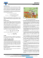
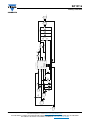
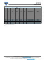
SiP12116
www.vishay.com
Vishay Siliconix
Reference Board User Manual for SiP12116 (3 A)
FEATURES
PRODUCT SUMMARY
Input Voltage Range
3 V to 15 V
Output Voltage range
0.6 V to 5.5 V
Operating Frequency
600 kHz
Continuous Output Current
Package
• 4.5 V to 15 V input voltage
• Adjustable output voltage down to 0.6 V
• 3 A continuous output current
• Operational frequency 600 kHz
3A
• 95 % peak efficiency
DFN10 - 3 mm x 3 mm
DESCRIPTION
The SiP12116 is a high frequency current-mode
constant-on-time (CM-COT) synchronous buck regulator
with integrated high-side and low-side power MOSFETs.
The SiP12116 is capable of 3 A continuous current.
This regulator provides an adjustable output voltage
which in standard setup can output 5 V down to 0.6 V
to accommodate a variety of applications, including
computing, consumer electronics, telecom, and industrial.
The CM-COT architecture delivers ultra-fast transient
response with minimum output capacitance and tight ripple
regulation at very light load. The parts are stable with any
capacitor type and no ESR network is required for loop
stability. The regulator integrates a full protection feature
set, it also has UVLO for the input rail and an internal
soft-start.
The SiP12116 is available in lead (Pb)-free power enhanced
3 mm x 3 mm DFN-10 package.
SPECIFICATIONS
This reference board allows the end user to evaluate the
SiP12116 chip for its features and all functionalities. It can
also be a reference design for a user's application.
• Stable with any capacitor. No external ESR network
required
• Ultrafast transient response
• Current mode constant on time
• Power saving scheme for increased light load efficiency
• ± 2 % accuracy of VOUT setting
• Cycle-by-cycle current limit
• Fully protected with OTP, SCP, UVP, OVP
• PGOOD indicator
• -40 °C to +125 °C operating junction temperature
APPLICATIONS
• Point of load regulation for low-power processors,
network processors, DSPs, FPGAs, and ASICs
• Low voltage, distributed power architectures with 5 V or
12 V rails
• Computing, broadband, networking, LAN / WAN, optical,
test, and measurement
• A/V, high density cards, storage, DSL, STB, DVR, DTV,
industrial PC
CONNECTION AND SIGNAL / TEST POINTS
Power Sockets
ORDERING INFORMATION
BOARD PART NUMBER MAX. OUTPUT CURRENT
VOUT
SiP12116DB
3.3 V
3A
VIN, GND (P1): input voltage source with VIN to be positive.
Connect to a voltage source:
SiP12116 - 3 V to 15 V
VOUT, GND (P2): output voltage with VOUT to be positive.
Connect to a load that draws no more than:
SiP12116 - 3 A
SELECTION JUMPERS
Enable
P3: this needs a jumper in place to disable the part. When
the jumper is removed the part will enable. It is advisable to
apply VIN and then enable the part.
SIGNALS AND TEST LEADS
Input Voltage Sense
VIN_SENSE, GNDIN_SENSE (P6): this allows the user to measure
the voltage at the input of the regulator and remove any
losses generated due to the, connections from the
measurement. This can also be used by a power source with
sense capability.
Revision: 03-Sep-14
Document Number: 63419
1
For technical questions, contact: [email protected]
THIS DOCUMENT IS SUBJECT TO CHANGE WITHOUT NOTICE. THE PRODUCTS DESCRIBED HEREIN AND THIS DOCUMENT
ARE SUBJECT TO SPECIFIC DISCLAIMERS, SET FORTH AT www.vishay.com/doc?91000
SiP12116
www.vishay.com
Output Voltage Sense
VOUT_SENSE, GNDOUT_SENSE (P5): this allows the user to
measure the voltage at the output of the regulator and
remove any losses generated due to the connections, from
the measurement. This can also be used by an active load
with sense capability.
Power Good Indication
PGD (P4): is an open drain output and is pulled up with a
10 kΩ resistor to VIN. When VFB is within ± 50 % percent
of the set voltage this pin will go HI to indicate the output
is okay.
POWER UP PROCEDURE
To turn-on the reference board, apply 12 V to VIN with the P3
jumper is in position (this disables the part).
To enable the part remove P3, a voltage can now be
observed at the output.
Note
• Note: When applying higher than 12 V to the input it is
reasonable to install a RC snubber from LX to GND. There are
place holders on the reference board R7 and C10 for the
snubber. Values of 10 Ω and 1 nF are a reasonable starting point.
ADJUSTMENTS TO THE REFERENCE BOARD
Output Voltage Adjustment
If a different output voltage is needed, simply change the
value of VOUT and solve for R3 based on the following
formula:
( V OUT - V FB )
R3 = R4 x ----------------------------------V FB
Where VFB is 0.6 V for the SiP12116.
Output Ripple Voltage
Output ripple voltage is measured with a tip and barrel
measurement across COUT. Typically output ripple voltage is
set to 3 % to 5 % of the output voltage, but an all ceramic
output solution can bring output ripple voltage to a much
lower level since the ESR of ceramics is very small.
If ceramics or a combination of ceramics and bulk
capacitors are used it may be necessary to add a voltage
injection network.
Inductor Selection
The choice of inductor is specific to each application and
quickly determined with the following equations:
V OUT
t on = ---------------------------------------V IN_MAX. × f SW
( V IN – V OUT ) × t on
L = ----------------------------------------------I OUT_MAX. × k
Where k is a percentage of maximum output inductor ripple
current required. The designer can quickly make a choice if
the ripple percentage is already decided based on the
system design; it should be noted that the SiP12116 uses
an internal current sense mechanism which translates as
the voltage ripple component. The SiP12116 requires a
Revision: 03-Sep-14
Vishay Siliconix
reasonable ripple current, we recommend around 50 % as a
start point.
Other than the inductance the DCR and saturation current
parameters are key values. The DCR causes an I2R loss
which will decrease the system efficiency and generate
heat. The saturation current has to be higher than the
maximum output current plus 1/2 the ripple current. In over
current condition the inductor current may be very high. All
this needs to be considered when selecting the inductor.
On this board Vishay IHLP series inductors are used to meet
cost requirement and high efficiency, a part that utilizes a
material that has incredible saturation levels compared to
competing products.
Output Capacitor Selection
Voltage rating, ESR, transient response, overall PCB area
and cost are requirements for selecting output capacitors.
The types of capacitors and there general advantages and
disadvantages are covered next.
Electrolytic have high ESR, dry out over time so ripple
current rating must be examined and have slower transient
response, but are fairly inexpensive for the amount of overall
capacitance.
Tantalums can come in low ESR varieties and high
capacitance value for its overall size, but they fail short when
damaged and also have slower transient response.
Ceramics have very low ESR, fast transient response and
overall small size, but come in low capacitance values
compared to the others above. A combination of technology
is sensible.
Enable Pin Voltage
The ENL pin will need to be set to enable the part. This pin
accepts an input voltage up to 5 V. On the reference design
the pin has a voltage divider from VIN. There is also a jumper,
P3, which shorts the pin to GND, this can be removed when
a suitable voltage has been applied to VIN enabling the
device.
Bootstrap Circuit
A bootstrap capacitor of 100 nF will be sufficient for this
circuit with a switching frequency of 600 kHz. A series
resistor has been added in order to slow down the low side
switch and minimize overshoot without adding a snubber.
This is user adjustable. This can be reduced to 0R to
improve efficiency.
VDD Decoupling
The VDD pin will need to be decoupled in order to provide a
stable voltage internally and externally. The value for this
capacitor is recommended as ≥ 1 μF.
Current Limit
The current limit is set internally to 4.8 A. This will include the
output current plus half of the ripple current. If the output
current is greater than this value the current limit will be
activated.
Document Number: 63419
2
For technical questions, contact: [email protected]
THIS DOCUMENT IS SUBJECT TO CHANGE WITHOUT NOTICE. THE PRODUCTS DESCRIBED HEREIN AND THIS DOCUMENT
ARE SUBJECT TO SPECIFIC DISCLAIMERS, SET FORTH AT www.vishay.com/doc?91000
SiP12116
www.vishay.com
Vishay Siliconix
Output Capacitance
The output capacitance will be determined by the ripple
voltage requirement. Voltage mode COT topology can work
with very small values of capacitor ESR however a ripple
injection network will also be required for stable operation.
9
7
2
The overall capacitance needs to be calculated next. The
following equations are used to calculate the size needed to
meet a transient load response:
10
VIN
I LPK = I OUT + 0.5 × I RIPPLE_MAX.
LX
1
4
2
C OUT_MIN.
L × ( I OUT + 0.5 × I RIPPLE_MAX. )
= -----------------------------------------------------------------------------------2
2
( V PK ) - ( V OUT )
Where ILPK is the peak inductor current, IRIPPLE_MAX. is the
maximum current ripple, IOUT is the maximum output
current, and VPK is the output voltage plus the rise on load
release.
Input Capacitance
In order to keep the design compact and minimize parasitic
elements, ceramic capacitors will be chosen. The initial
requirement for the input capacitance is decided by the
maximum input voltage, 15 V in this case however a 35 V
rated capacitor will be chosen of the X7R variety.
In order to determine the minimum capacitance the input
voltage ripple needs to be specified; VCINPP ≤ 150 mV is a
suitable starting point. This magnitude is determined by the
final application specification. The input current needs to be
determined for the lowest operating input voltage:
I OUT
I CIN ( RMS ) = ------------ × V OUT × ( V IN - VOUT )
V IN
The minimum input capacitance can then be found,
DC- ( 1- DC )
C IN_MIN. = I OUT × ----------------------------------V CINPP × f SW
Snubber
Provision has been made for a snubber on the underside of
the board which the user might need to consider populating
if a higher input voltage is required.
LAYOUT CONSIDERATIONS
The SiP12116 offers the designer a compact buck regulator
solution. If the below layout recommendations are followed,
the same layout can be used to cover a wide range of output
currents and voltages without any changes to the board
design and only minor changes to the component values in
the schematic.
The reference design has a majority of the components
placed on the top layer. This allows for easy assembly and
straightforward layout.
Figure 1 outlines the pointers for the layout considerations
and the explanations follow.
Revision: 03-Sep-14
6
0V
8
5
3
11
VOUT
5
Fig. 1 - Reference Design Pointers
1. Place input ceramic capacitors close to the voltage input
pins with a small 10 nF/100 nF placed as close as the
design rules will allow. This will help reduce the size of
the input high frequency current loop and consequently
reduce the high frequency ripple noise seen at the input
and the LX node.
2. Place the setup and control passive devices logically
around the IC with the intention of placing a quiet ground
plane beneath them on a secondary layer.
3. It is advisable to use ceramic capacitors at the output to
reduce impedance. Place these as close to the IC PGND
and output voltage node as design will allow. Place a
small 10 nF/100 nF ceramic capacitor closest to the IC
and inductor loop.
4. The loop between LX, VOUT and the IC GND should be as
compact as possible. This will lower series resistance
and also make the current loop smaller enabling the high
frequency response of the output capacitors to take
effect.
5. The output impedance should be small when high
current is required; use high current traces, multiple
layers can be used with many vias if the design allows.
6. Use many vias when multiple layers are involved. This
will have the effect of lowering the resistance between
layers and reducing the via inductance of the PCB nets.
7. The quiet AGND should be connected to the PGND plane
near to the input GND at one connection only of at least
1 mm width.
8. PGND can be used on internal layers if the resistance of
the PCB is to be small; this will also help remove heat.
Use extra vias if needed but be mindful to allow a path
between the vias.
9. A quiet plane should be employed for the AGND, this is
placed under the small signal passives. This can be
placed on multiple layers if needed for heat removal.
10. The LX copper can also be used on multiple layers, use
a number of vias.
11. The copper area beneath the inductor has been removed
(on all layers) in this design to reduce the inductive
coupling that occurs between the inductor and the GND
trace. No other voltage planes should be placed under
this area.
Document Number: 63419
3
For technical questions, contact: [email protected]
THIS DOCUMENT IS SUBJECT TO CHANGE WITHOUT NOTICE. THE PRODUCTS DESCRIBED HEREIN AND THIS DOCUMENT
ARE SUBJECT TO SPECIFIC DISCLAIMERS, SET FORTH AT www.vishay.com/doc?91000
SiP12116
www.vishay.com
Vishay Siliconix
PCB LAYOUT
Revision: 03-Sep-14
Fig. 2 - Top Layer
Fig. 4 - Inner Layer 2
Fig. 3 - Inner Layer 1
Fig. 5 - Bottom Layer
Document Number: 63419
4
For technical questions, contact: [email protected]
THIS DOCUMENT IS SUBJECT TO CHANGE WITHOUT NOTICE. THE PRODUCTS DESCRIBED HEREIN AND THIS DOCUMENT
ARE SUBJECT TO SPECIFIC DISCLAIMERS, SET FORTH AT www.vishay.com/doc?91000
SiP12116
www.vishay.com
Vishay Siliconix
Header 2
R4
1K
OMIT
3.3μ
C9
L1
100n
VFB
LX
VCC
C4
5V 2
PGD
10μ
10μ
10n
C2
C1
Header 2
Revision: 03-Sep-14
Header 2
P6
1
2
Header 2
P3
1
2
0V
P4
R1
4K53
1
2
0V
Terminal
P1
1
2
0V
VIN
C3
R5
1K
10K
PGD9
R6
1μ
LX
EN 10
EN
VIN
3
U1
GND
GND
GND
4
5
P1
SiP12116
BOOT
0V
6
1 VFB
LX
7
8 BS R2
20R
BS_1
C5
Terminal
22μ
22μ
R3
4K53
10n
C6
C7
VOUT
C8
P2
1
2
P5
1
2
SCHEMATIC
Document Number: 63419
5
For technical questions, contact: [email protected]
THIS DOCUMENT IS SUBJECT TO CHANGE WITHOUT NOTICE. THE PRODUCTS DESCRIBED HEREIN AND THIS DOCUMENT
ARE SUBJECT TO SPECIFIC DISCLAIMERS, SET FORTH AT www.vishay.com/doc?91000
SiP12116
www.vishay.com
Vishay Siliconix
BILL OF MATERIAL VIN = 12 V, VOUT = 3.3 V, fsw = 600 kHz
ITEM
QTY
REFERENCE
PCB
FOOTPRINT
VALUE
VOLTAGE
1
2
C1, C2
1210
10 μF
35 V
C1210C106M6PACTU
KEMET
2
2
C3, C6
0402
10 nF
50 V
GRM155R71H103KA88D
MURATA
3
1
C4
0603
1 μF
10 V
C0402C105M8PACTU
KEMET
4
1
C5
0402
100 nF
35V
CGA2B3X7R1V104K050BB
VISHAY
5
2
C7, C8
0805
22 μF
10 V
CL21A226MPQNNNE
SAMSUNG
6
1
R2
0402
20 Ω
-
CRCW040220R0FKED
VISHAY
7
1
R3
0402
4.53 kΩ
-
CRCW04024K53FKED
VISHAY
8
1
R4
0402
1 kΩ
-
CRCW0402249KFKED
VISHAY
9
1
L1
IHLP2525
3.3 μH
-
IHLP2020BZER3R3M01
VISHAY
10
1
U1
DFN10-3x3
-
-
SiP12116
VISHAY
11
1
R1
0402
4.53 kΩ
-
CRCW04024K53FKED
VISHAY
12
1
R5
0402
1 kΩ
-
CRCW0402249KFKED
VISHAY
13
1
R6
0402
10 kΩ
-
CRCW040210K0FKED
VISHAY
14
4
P3, P4, P5, P6
HDR1x2
-
-
90120-0126
MOLEX
15
2
P1, P2
TERM2
-
-
282834-2
TE CONNECTIVITY
PART NUMBER
MANUFACTURER
Note
Only needed for reference board
Revision: 03-Sep-14
Document Number: 63419
6
For technical questions, contact: [email protected]
THIS DOCUMENT IS SUBJECT TO CHANGE WITHOUT NOTICE. THE PRODUCTS DESCRIBED HEREIN AND THIS DOCUMENT
ARE SUBJECT TO SPECIFIC DISCLAIMERS, SET FORTH AT www.vishay.com/doc?91000