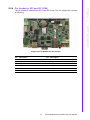
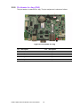
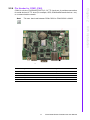
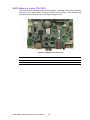
1
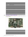
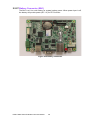
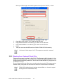
User Manual
PCM-C3500 Series
Evaluation Kit
(PCM-C3530/PCM-C3503)
TI OMAP35x Processor - ARM®
CortexTM A8 Architecture
Copyright
The documentation and the software included with this product are copyrighted 2011
by Advantech Co., Ltd. All rights are reserved. Advantech Co., Ltd. reserves the right
to make improvements in the products described in this manual at any time without
notice. No part of this manual may be reproduced, copied, translated or transmitted
in any form or by any means without the prior written permission of Advantech Co.,
Ltd. Information provided in this manual is intended to be accurate and reliable. However, Advantech Co., Ltd. assumes no responsibility for its use, nor for any infringements of the rights of third parties, which may result from its use.
Acknowledgements
Intel and Pentium are trademarks of Intel Corporation.
Microsoft Windows and MS-DOS are registered trademarks of Microsoft Corp.
All other product names or trademarks are properties of their respective owners.
Part No. 2002353000
Edition 1
Printed in Taiwan
August 2011
PCM-C3500 Series Evaluation Kit User Manual
ii
Packing List
Before setting up the system, check that the items listed below are included and in
good condition. If any item does not accord with the table, please contact your dealer
immediately.
PCM-C3530 (P/N: PCM-C3530-668B0E)/PCM-C3503 (P/N: PCM-C3503650B0E)
LCD-LED Backlight 7" LVDS RGB 97G070V1N0F-2 (P/N: 1330002308)
Touch Cable (P/N: 1700000194)
LVDS Cable (P/N: 1700014418)
LCD Backlight Cable (P/N: 1700014438)
ADAPTER 100-240V 90W 19V 4.74A W/PFC 9NA0900508 (P/N: 1757002944)
Wide-Temp RS-232 to RS-422/485 Converter (P/N: ADAM-4520I-AE)
PLUG-IN BLOCK DIP 2P (F) MC421-38102 DECA (P/N: 1652002209)
A Cable D-SUB 9P(M)/2*5P-2.0 15cm *2 (P/N: 1703100153)
M Cable D-SUB 9P(F)/D-SUB 9P(F) 100CM (P/N: 1700091002)
Terminal connector 9P Female (P/N: 1654909900)
CD-ROM for PCM-C3530 evaluation kit V1.0
USB Type-A Cable (P/N: 1700019129)
Mini USB Client Cable (P/N: 1700019077)
Mini USB Host Cable (P/N: 1700019076)
SQFlash SD Card SLC 2G, 2CH(-40~85° C) (P/N: SQF-ISDS2-2G-ETE)
3 pin Power Cord for USA standard (option) (P/N: 1700001524)
3 pin Power Cord for Europe standard (option) (P/N: 170203183C)
3 pin Power Cord for UK standard (option) (P/N: 170203180A)
iii
PCM-C3500 Series Evaluation Kit User Manual
Safety Instructions
1.
2.
3.
Read these safety instructions carefully.
Keep this User Manual for later reference.
Disconnect this equipment from any AC outlet before cleaning. Use a damp
cloth. Do not use liquid or spray detergents for cleaning.
4. For plug-in equipment, the power outlet socket must be located near the equipment and must be easily accessible.
5. Keep this equipment away from humidity.
6. Put this equipment on a reliable surface during installation. Dropping it or letting
it fall may cause damage.
7. The openings on the enclosure are for air convection. Protect the equipment
from overheating. DO NOT COVER THE OPENINGS.
8. Make sure the voltage of the power source is correct before connecting the
equipment to the power outlet.
9. Position the power cord so that people cannot step on it. Do not place anything
over the power cord.
10. All cautions and warnings on the equipment should be noted.
11. If the equipment is not used for a long time, disconnect it from the power source
to avoid damage by transient overvoltage.
12. Never pour any liquid into an opening. This may cause fire or electrical shock.
13. Never open the equipment. For safety reasons, the equipment should be
opened only by qualified service personnel.
14. If one of the following situations arises, get the equipment checked by service
personnel:
The power cord or plug is damaged.
Liquid has penetrated into the equipment.
The equipment has been exposed to moisture.
The equipment does not work well, or you cannot get it to work according to
the user's manual.
The equipment has been dropped and damaged.
The equipment has obvious signs of breakage.
DISCLAIMER: This set of instructions is given according to IEC 704-1. Advantech
disclaims all responsibility for the accuracy of any statements contained herein.
PCM-C3500 Series Evaluation Kit User Manual
iv
Contents
Chapter
Chapter
1
Overview...............................................1
1.1
1.2
1.3
1.4
Introduction ............................................................................................... 2
Features .................................................................................................... 3
Hardware Specification ............................................................................. 4
Board Block Diagram ................................................................................ 6
Figure 1.1 Board Block Diagram.................................................. 6
2
H/W Installation....................................7
2.1
Development Kit H/W Installation.............................................................. 8
Figure 2.1 PCM-C3530 Development Kit Assembly.................... 9
2.1.1 PCM-C3530/3503 (Part-A).......................................................... 10
2.1.2 LVDS LCD Module (Part-B) ........................................................ 10
2.1.3 Touch Cable (Part-C).................................................................. 10
2.1.4 LVDS Cable (Part-D) .................................................................. 10
2.1.5 LCD Backlight Cable (Part-E) ..................................................... 10
2.1.6 Keypad (Part-F) .......................................................................... 10
2.1.7 Keypad Cable (Part-G) ............................................................... 10
2.1.8 Speaker & Audio Cables (Part-H) ............................................... 10
2.1.9 UART Port Cable (D-SUB 9P to Housing) (Part-I)...................... 10
2.1.10 Button Cable (Part-J) .................................................................. 10
2.1.11 USB Type-A Cable (Part-K) ........................................................ 11
2.1.12 ADAM-4520I (Part-L) .................................................................. 11
2.1.13 2P Plug-in Terminal Block (Part-M) ............................................ 11
2.1.14 Mini USB Client Cable (Part-N)................................................... 11
2.1.15 Mini USB Host Cable (Part-O) .................................................... 11
2.1.16 D-SUB 9P Serial Cable (Part-P) ................................................. 11
2.1.17 Terminal Connector 9P Female (Part-Q) .................................... 11
2.1.18 19 V Power Adapter (Part-R) ...................................................... 11
2.1.19 Power Cord (Part-S) ................................................................... 11
Connector Settings.................................................................................. 11
2.2.1 Pin Header for 20x Pins GPIO (CN1) ......................................... 12
Figure 2.2 Pin Header for GPIO ................................................ 12
2.2.2 Pin Header for SD2 (CN2) .......................................................... 13
Figure 2.3 Pin Header for SD2 .................................................. 13
2.2.3 Pin Header for Matrix Keypad (CN3) .......................................... 14
Figure 2.4 Pin Header for Matrix Keypad .................................. 14
2.2.4 Pin Header for SPI and I2C (CN4).............................................. 15
Figure 2.5 Pin Header for SPI and I2C ...................................... 15
2.2.5 Pin Header for Jtag (CN5) .......................................................... 16
Figure 2.6 Pin Header for Jtag................................................... 16
2.2.6 Pin Header for COM1 (CN6)....................................................... 17
Figure 2.7 Pin Header for UART1.............................................. 17
2.2.7 Pin Header for Reset (CN7)........................................................ 18
Figure 2.8 Pin Header for Reset ................................................ 18
2.2.8 Box Header for LINE-OUT, LINE-IN, MIC-IN and L&R Speakers
(CN8) .......................................................................................... 19
Figure 2.9 Box Header for LINE-OUT, LINE-IN, MIC-IN and L&R
Speakers .................................................................. 19
2.2.9 Pin Header for COM3 RS-232 (Debug Port) (CN9) .................... 20
Figure 2.10Pin Header for COM3 RS-232 (Debug Port) ............ 20
2.2.10 Wafer for 12 V backlight (CN10) ................................................ 21
Figure 2.11Wafer for 12 V Backlight........................................... 21
2.2.11 Wafer for 4-wire T/S (CN11) ....................................................... 22
2.2
v
PCM-C3500 Series Evaluation Kit User Manual
2.3
Chapter
Figure 2.12Wafer for 4-wire T/S ................................................. 22
2.2.12 Pin Header for Suspend (CN12)................................................. 23
Figure 2.13Pin Header for Suspend ........................................... 23
2.2.13 LVDS LCD Connector (CN13) .................................................... 24
Figure 2.14LVDS LCD Connector .............................................. 24
2.2.14 Pin Header for USB4 (CN14)...................................................... 25
Figure 2.15Pin Header for USB4................................................ 25
2.2.15 RS-485 Terminal Block (CN15) .................................................. 26
Figure 2.16RS-485 Terminal Block ............................................ 26
Figure 2.17RS-485 Bus .............................................................. 26
Figure 2.18Schematic about RS-485 of PCM-C3500................. 26
2.2.16 Pin Header for USB3 (CN16)...................................................... 27
Figure 2.19Pin Header for USB3................................................ 27
2.2.17 Pin Header for COM2 RS-232 (CN18) ....................................... 28
Figure 2.20Pin Header for COM2 RS-232.................................. 28
2.2.18 LAN Connector with LEDs (CN19) ............................................. 29
Figure 2.21LAN Connector with LEDs........................................ 29
2.2.19 USB 1&2 (Standard Type-A) (CN21).......................................... 30
Figure 2.22USB1 & 2 (Standard Type-A) ................................... 30
2.2.20 DC-IN Power Jack (CN22).......................................................... 31
Figure 2.23DC-IN Power Jack.................................................... 31
2.2.21 USB OTG MINI-AB Connector (CN23)....................................... 32
Figure 2.24USB OTG MINI-AB Connector ................................. 32
2.2.22 COM4 RS-232 (D-SUB9 Connector) (CN25) ............................. 33
Figure 2.25COM4 RS-232 (D-SUB9) ......................................... 33
2.2.23 SD/MMC Slot (CN26) ................................................................. 34
Figure 2.26SD/MMC Slot............................................................ 34
2.2.24 Power Rail for Battery Charger Board (CN28)............................ 35
Figure 2.27Power Rail for Battery Charger Board...................... 35
2.2.25 Control Signal for Battery Charger Board (CN29) ...................... 36
Figure 2.28Control Signal for Battery Charger Board................. 36
2.2.26 Power ON/OFF Switch (SW1) .................................................... 37
Figure 2.29Power ON/OFF Switch ............................................. 37
2.2.27 Battery Connector (BH1) ............................................................ 38
Figure 2.30Battery Connector .................................................... 38
Mechanical.............................................................................................. 39
2.3.1 Connector Location..................................................................... 39
Figure 2.31PCM-C3530/3503 Position-Top ............................... 39
Figure 2.32PCM-C3530/3503 Position-Bottom .......................... 39
2.3.2 Board Dimension ........................................................................ 40
Figure 2.33PCM-C3530/3503 Dimension Top ........................... 40
Figure 2.34PCM-C3530/3503 Dimension Bottom ...................... 40
3
Software Functionality ..................... 41
3.1
Operating System Introduction ............................................................... 42
Figure 3.1 Windows® CE 6.0 on the PCM-C3530/3503 Platform .
42
Windows CE Startup Procedure ............................................................. 43
3.2.1 Booting from SD Storage Card ................................................... 43
Figure 3.2 HP USB DISK Storage Format Tool......................... 44
3.2.2 Booting from Onboard Flash Chip .............................................. 44
Figure 3.3 Storage Manager Setting ......................................... 45
Figure 3.4 Format Setting.......................................................... 46
Figure 3.5 Mount On-board Flash Disk ..................................... 46
Utilities .................................................................................................... 47
3.3.1 Test Utility ................................................................................... 47
Figure 3.6 Test Utility................................................................. 48
3.3.2 Startup Execution ....................................................................... 48
3.2
3.3
PCM-C3500 Series Evaluation Kit User Manual
vi
3.3.3
3.4
Platform Setting .......................................................................... 48
Figure 3.7 General Information.................................................. 49
Figure 3.8 Display Configuration ............................................... 49
Figure 3.9 Watchdog Timer ....................................................... 50
Figure 3.10Audio Settings .......................................................... 51
Figure 3.11Miscellaneous Settings............................................. 52
Network ................................................................................................... 53
Figure 3.12Networking via Ethernet ........................................... 53
vii
PCM-C3500 Series Evaluation Kit User Manual
PCM-C3500 Series Evaluation Kit User Manual
viii
Chapter
1
1
Overview
This chapter briefly introduces the
PCM-C3500 Series products.
1.1 Introduction
An evaluation kit for RISC based Design to Order Service (DTOS) projects. In order
to provide DTOS customers with an efficient/ risk free evaluation tool, Advantech provides many kinds of RISC based evaluation kits. Before DTOS projects kick-off, customer can use the kit to evaluate everything in detail. The OS ready kit is equipped
with all the necessary H/W and S/W tools a customer needs, so it can shorten evaluation and speed up user target application development.
Note!
The purpose of the kit is for potential RISC-based DTOS project evaluation only...NOT for SBC sales.
The PCM-C3530/3503 is designed as a solution board, using TI OMAP3530/3503
processor based on ARM® CortexTM A8 architecture, which is a complete 32-bit, (up
to) 600 MHz speed SoC engine. It provides customers with a high performance
board subsystem for evaluation. With flexible I/O interfaces and complete hardware
and software solution, the PCM-C3530/3503 is a fast time-to-market platform for customers to develop their applications and products easily prior to system integration.
The PCM-C3530/3503 Evaluation Kit is a complete system and integrates all solutions developers need, based on the PCM-C3530/3503 module board, into a package that provides customers with a platform for project evaluation, application
development, and solution feasibility testing that decreases lead-time and lowers initial expense. The PCM-C3530/3503 Evaluation Kit has already integrated certified
functions under Linux's test kits giving project development and implementation an
easy and risk-free start.
PCM-C3500 Series Evaluation Kit User Manual
2
PCM-C3530/3503 uses TI OMAP3530/3503 Processor - ARM® CortexTM A8 architecture. The platform is a, compact, reliable system with great power management—
without a heaksink. The platform is good for the following applications:
Economical HMI (Human Machine Interface)
Self Service / Access Control
Fleet management / Navigation
Hand-held data collector
Built-in 430-MHz TMS320C64x+TM DSP Core (PCM-C3530 only)
Supports Mpeg 1/2/4 H.264 decode/encode. Video supports D1 resolution
directly and up to 720P*
H/W 2D/3D Accelerator directly supports OpenGLES 1.1 and 2.0, OpenVG1.0
(PCM-C3530 only)
WinCE 6.0 (default)/ Linux O.S. supports.
Rich I/O as LCD out, Audio, USB, LAN, multi-COM, SD(2), GPIO(20), I2C(2),
SPI(1), Keypad 6X6
Supports wide working temperature -40 ~ 85° C (optional)
*Needs use 3rd party codec support for 720P.
3
PCM-C3500 Series Evaluation Kit User Manual
Overview
The main features of TI OMAP3530/3503 Processor are:
ARM Cortex A8 600 MHz kernel
Chapter 1
1.2 Features
1.3 Hardware Specification
Item
Description
Kernel
CPU
PCM-C3530: TI OMAP3530 ARM Cortex A8 600 MHz
PCM-C3503: TI OMAP3503 ARM Cortex A8 600 MHz
DSP
Built-in 430-MHz TMS320C64x+™ DSP Core (PCM-C3530 only)
2D/3D Accelerators
Yes, support OpenGLES 1.1 and 2.0, OpenVG1.0
(PCM-C3530 only)
O.S
WinCE6.0 English professional version as default, and Linux
DRAM
PCM-C3530: 256 MB
PCM-C3503: 128 MB (Optional: 256 MB)
Onboard Flash
PCM-C3530: Default 2 GB, (Optional: 0 GB, 1 GB)
PCM-C3503: Default 0 GB, (Optional: 1 GB, 2 GB)
RTC
Yes
Watchdog
Yes
Power Management
-Standard mode
-Idle mode
-Suspend mode
I/O
COM
PCM-C3530 (5 x COMs):
-COM1, 3.3 V TTL, 4–wire
-COM2, RS-232, 4-wire
-COM3, RS-232, 4–wire (Debug port)
-COM4, RS-232, Full Function (D-Sub9)
-COM5, RS-485 (2-pin Phoenix Connector)
===================================================
PCM-C3503 (3 x COMs):
-COM1, 3.3 V TTL, 4–wires.
-COM2, RS-232, 4-wires
-COM3, RS-232, 4–wires. (Debug port)
USB Port
4 x USB 2.0 host (High speed, 2 x Type A, 2 x pin header)
USB OTG
1 x USB 2.0 OTG (High speed)
LAN
1 x 10/100 BASE-T (RJ-45)
SD/MMC
2 x SDIO/MMC interface (SD slot x 1+ pin header x 1)
GPIO
20 x pins 3.3 V TTL level DIO
Hotkey/matrix key pad Support 6 x 6 matrix keypad
I2C
2x
SPI
1x
Buzzer control
Yes
Display
Graphic Chip
CPU internal 24-bits LCD controller
LCD Resolution
Default: 800 x 480 7” WVGA
Optional: 320 x 240 ~ 1280 x 800
Brightness/
Backlight Control
Yes
T/S
4-wire resistive type interface
Video Interface
1 x LVDS
Audio
Audio Codec for Line-in, Line-out, Speak-Out & Mic-in
PCM-C3500 Series Evaluation Kit User Manual
4
DC-input
10 ~ 24 V ± 5%
Power Consumption
Standard 2 W ( Max 3 W)
Power Control
1 x Power Switch
1 x H/W reset (Pin header)
1 x Suspend (Pin header)
Mechanical and Environmental
90 mm x 120 mm x 17 mm ( PCB thickness 1.6 mm)
Weight
92 g
Operation Temperature
0 ~ 60° C (32 ~ 140° F)
(-20 ~ 70° C ; -40 ~ 85° C by component change)
Operating Humidity
5% ~ 95% Relative Humidity, non condensing
Vibration
3.5 G, 1000 times
Others
RoHS
Yes
Certification
CE/FCC Class A
5
PCM-C3500 Series Evaluation Kit User Manual
Overview
Board size
Chapter 1
Power
1.4 Board Block Diagram
Figure 1.1 Board Block Diagram
PCM-C3500 Series Evaluation Kit User Manual
6
Chapter
2
2
H/W Installation
This chapter explains the setup
procedures of the PCM-C3530/
3503 hardware, including instructions on setting jumpers and connecting peripherals, switches,
indicators and mechanical drawings. Be sure to read all safety
precautions before you begin the
installation procedure.
2.1 Development Kit H/W Installation
Figure 2.1 is PCM-C3530/3503 Evaluation Kit Assembly, the detailed description and
Advantech P/N are shown below.
Item
Description
Advantech P/N
Part-A
PCM-C3530
PCM-C3503
(P/N: PCM-C3530-668B0E)
(P/N: PCM-C3503-650B0E)
Part-B LCD-LED Backlight 7" LVDS RGB 97G070V1N0F-2 (P/N: 96LEDK-A070WV32RB1)
Part-C Touch Cable
(P/N: 1700000194)
Part-D LVDS Cable
(P/N: 1700014418)
Part-E LCD Backlight Cable
(P/N: 1700014438)
Part-F Keypad (option)
(P/N: 96969315A0E)
Part-G 6*6 Keypad Cable (option)
(P/N: 1700004515)
Part-H Speaker & Audio Cables
(P/N: 1700019546)
Part-I
(P/N: 1703100153)
Cable D-SUB 9P(M)/2*5P-2.0 15 CM
Part-J Button Cable
(P/N: 1700003414)
Part-K USB Type-A Cable
(P/N: 1700019129)
Part-L Wide-Temp RS-232 to RS-422/485 Converter
(P/N: ADAM-4520I-AE)
Part-M PLUG-IN BLOCK DIP 2P (F) MC421-38102 DECA (P/N: 1652002209)
Part-N Mini USB Client Cable
(P/N: 1700019077)
Part-O Mini Host Cable
(P/N: 1700019076)
Part-P M Cable D-SUB 9P(F)/D-SUB 9P(F) 100 CM
(P/N: 1700091002)
Part-Q Terminal connector 9P Female
(P/N: 1654909900)
ADAPTER 100-240 V 90 W 19 V 4.74 A W/PFC
Part-R
9NA0900508
(P/N: 1757002944)
3 pin Power Cord (USA Standard)
Part-S 3 pin Power Cord (Europe standard)
3 pin Power Cord (UK standard)
(P/N: 1700001524)
(P/N: 170203183C)
(P/N: 170203180A)
PCM-C3500 Series Evaluation Kit User Manual
8
Chapter 2
H/W Installation
Figure 2.1 PCM-C3530 Development Kit Assembly
9
PCM-C3500 Series Evaluation Kit User Manual
2.1.1 PCM-C3530/3503 (Part-A)
PCM-C3530/3503 is a best-cost, low-power, performance SBC (Single Board Computer) without a heatsink, geared to satisfy the needs for various industrial computing
equipment. Based on TI OMAP3530/3503 Processor - ARM® CortexTM A8 architecture, there are DDR SDRAM, iNAND flash and other main ICs. PCM-C3530/3503
offers convenient connector layout, easy assembly, multiple I/O, and includes one 10/
100Mbps Ethernet, four USB (Universal Serial Bus) 2.0 and five serial ports for easy
system expansibility.
2.1.2 LVDS LCD Module (Part-B)
A 7.0 inch color TFT-LCD Module with 4-wire resistive type touch sensor. The module is designed with wide viewing angle; wide operating temperature and long life
LED backlight, which makes it well suited to be a display unit for Industrial Applications. An LED driving board for the backlight unit is included in this panel and the
structure of the LED units are replaceable. It's built in timing controller and LVDS
interface. The display supports the WVGA (800 (H) x 480(V)) screen format and 16.2
M colors (RGB 24-bit) or 262 K (RGB 18-bit) selectable.
2.1.3 Touch Cable (Part-C)
The touch cable connects PCM-C3530/3503 (CN11) and the touch connector of the
7" LVDS LCD Module.
2.1.4 LVDS Cable (Part-D)
The LVDS cable connects PCM-C3530/3503 (CN23) and the LCD signal connector
of the 7" LVDS LCD Module.
2.1.5 LCD Backlight Cable (Part-E)
The LVDS backlight cable connects PCM-C3530/3503 (CN10) and the LCD backlight
connector of the 7" LVDS LCD Module.
2.1.6 Keypad (Part-F)
8 x 8 arrays of 64 normally open, single-pole switches. (6 x 6 region of keypad are
available on PCM-C3530/3503.)
2.1.7 Keypad Cable (Part-G)
The keypad cable connects PCM-C3530/3503 (CN3) and keypad.
2.1.8 Speaker & Audio Cables (Part-H)
The cable connects PCM-C3530/3503 (CN8) and LINE-OUT, LINE-IN, MIC-IN and
L&R Speakers.
2.1.9 UART Port Cable (D-SUB 9P to Housing) (Part-I)
The cable uses to extend UART port 9pin header from PCM-C3530/3503 to D-SUB
9P serial port connector.
2.1.10 Button Cable (Part-J)
The button cable connects to PCM-C3530/3503 (CN7 and 12) for reset and suspend.
PCM-C3500 Series Evaluation Kit User Manual
10
The USB extend cable provide Type-A for USB device.
2.1.12 ADAM-4520I (Part-L)
The ADAM-4520I converter transparently converts RS-232 signals into isolated RS422 or RS-485 signals. It uses for RS-485 function (CN15) of PCM-C3530/3503 for
testing.
The terminal block with extra 2 cables connects PCM-C3530/3503 (CN15) and
ADAM-4520I (RS-485 side).
2.1.14 Mini USB Client Cable (Part-N)
The mini USB client cable (P/N: 1700019077) connects PCM-C3530/3503 (CN23)
and one USB host device.
2.1.15 Mini USB Host Cable (Part-O)
The mini USB host cable (P/N: 1700019076) connects PCM-C3530/3503 (CN23)
and one USB client device.
2.1.16 D-SUB 9P Serial Cable (Part-P)
The serial cable connects PCM-C3530/3503 COM ports and serial device.
2.1.17 Terminal Connector 9P Female (Part-Q)
The terminal connector 9P female is used for RS-232 loopback function testing.
2.1.18 19 V Power Adapter (Part-R)
This is an AC to DC power device, it can provide for a 19 V DC output (60 W max)
with constant voltage sources (100 V ~ 240 V).
2.1.19 Power Cord (Part-S)
3P Power Cord (USA, Europe or UK standard) for 19 V Power Adapter AC input.
2.2 Connector Settings
The following table shows the connector list of PCM-C3530/3503.
Connector
Description
CN 1
Pin Header for 20x pins GPIO
CN 2
Pin Header for SD2
CN 3
Pin Header for Matrix Keypad
CN 4
Pin Header for SPI and I2C
CN 5
Pin Header for Jtag
CN 6
Pin Header for COM1
CN 7
Pin Header for Reset
CN 8
Box Header for LINE-OUT, LINE-IN, MIC-IN and L&R Speakers
CN 9
Pin Header for COM3, RS-232, debug port
11
PCM-C3500 Series Evaluation Kit User Manual
H/W Installation
2.1.13 2P Plug-in Terminal Block (Part-M)
Chapter 2
2.1.11 USB Type-A Cable (Part-K)
CN10
Wafer for 12 V backlight
CN11
Wafer for 4-wire T/S
CN12
Pin Header for Suspend
CN13
LVDS LCD Connector
CN14
Pin Header for USB4
CN15
RS-485 Terminal Block
CN16
Pin Header for USB3
CN18
Pin Header for COMx, RS-232
CN19
Ethernet LAN Connector
CN21
USB1&2 (Standard Type-A)
CN22
DC-IN Power Jack
CN23
USB OTG MINI-AB Connector
CN25
COM4, RS-232, D-SUB9 Connector
CN26
SD/MMC Slot
CN27
Power rail for battery charger board
CN28
Control signal for battery charger board
SW1
Power ON/OFF Switch
BH1
Battery Connector
2.2.1 Pin Header for 20x Pins GPIO (CN1)
This pin header is extended for 20 x pins 3.3V TTL Level GPIO. The pin assignment
is shown as follows.
Figure 2.2 Pin Header for GPIO
Pin
Description
1
GND
2
3.3 V
3
GPIO_1
4
GPIO_2
5
GPIO_3
6
GPIO_4
7
GPIO_5
8
GPIO_6
9
GPIO_7
10
GPIO_8
PCM-C3500 Series Evaluation Kit User Manual
Pin
12
Description
GPIO_9
12
GPIO_10
13
GPIO_11
14
GPIO_12
15
GPIO_13
16
GPIO_14
17
GPIO_15
18
GPIO_16
19
GPIO_17
20
GPIO_18
21
GPIO_19
22
GPIO_20
Chapter 2
11
2.2.2 Pin Header for SD2 (CN2)
Figure 2.3 Pin Header for SD2
Pin
Description
Pin
Description
1
GND
2
GND
3
MMC3_DAT1
4
MMC3_CLK
5
MMC3_DAT0
6
MMC3_CMD
7
MMC3_DAT3
8
MMC3_nMCCD
9
MMC3_DAT2
10
3.3 V
11
SDIO_nWAIT
12
SDIO_WLAN_LED
13
PCM-C3500 Series Evaluation Kit User Manual
H/W Installation
The SD/MMC slots are 3.3 V powered. It can be extended for a SD slot module and
WIFI module use. It includes the following features.
Full compatibility with the MMC system specification version 3.2
Compatibility with the SD Memory Card specification 1.01, and SD I/O specification 1.1 with 1/4 channel (s)
Block-based data transfer between MMC card and SDHC (stream mode not
supported)
100 Mbps maximum data rate in 4-bit mode, SD bus clock up to 25 MHz
2.2.3 Pin Header for Matrix Keypad (CN3)
The keypad circuitry scans a 6 x 6 array of 36 normal-open, single-pole switches.
Any one or two keys depressed will be de-bounced and decoded. An interrupt is generated whenever a stable set of depressed keys is detected. The keypad interface:
Provides scanning, de-bounce, and decoding for a 36-key switch array
Scans an 6-row by 6-column matrix
May decode 2 keys at once
Generates an interrupt when a new stable key is determined
Also generates a 3-key reset interrupt
Figure 2.4 Pin Header for Matrix Keypad
Pin
Description
Pin
Description
1
KEY_COL0
2
KEY_ROW0
3
KEY_COL1
4
KEY_ROW1
5
KEY_COL2
6
KEY_ROW2
7
KEY_COL3
8
KEY_ROW3
9
KEY_COL4
10
KEY_ROW4
11
KEY_COL5
12
KEY_ROW5
PCM-C3500 Series Evaluation Kit User Manual
14
This pin header is extended for SPI*1 and I2C*2 sets. The pin assignment is shown
as following.
Chapter 2
2.2.4 Pin Header for SPI and I2C (CN4)
H/W Installation
Figure 2.5 Pin Header for SPI and I2C
Pin
Description
Pin
Description
1
GND
2
SPI_IRQ
3
I2C_CLK2
4
SPI_SOMI
5
I2C_DAT2
6
SPI_SIMO
7
I2C_CLK3
8
SPI_CS0
9
I2C_DAT3
10
SPI_CLK
11
3.3 V
12
3.3 V
15
PCM-C3500 Series Evaluation Kit User Manual
2.2.5 Pin Header for Jtag (CN5)
This pin header is extended for Jtag. The pin assignment is shown as follows.
Figure 2.6 Pin Header for Jtag
Pin
Description
Pin
Description
1
1.8 V
2
JTAG_TMS
3
JTAG_nRST
4
JTAG_TDI
5
GND
6
JTAG_TDO
7
JTAG_RTCK
8
JTAG_TCK
9
JTAG_EMU1
10
JTAG_EMU0
PCM-C3500 Series Evaluation Kit User Manual
16
COM1 is a 4-wire (TXD/RXD/RTS/CTS) 3.3 V TTL Level port. It provides connections
for serial devices in TTL level (For example, GPS, GSM and Bluetooth devices...etc.)
or a communication network.
Note!
The max. baud rate between PCM-C3500 to PCM-C3500 is 38400.
Chapter 2
2.2.6 Pin Header for COM1 (CN6)
H/W Installation
Figure 2.7 Pin Header for UART1
Pin
Description
Pin
Description
1
N/C
2
UART1_RX
3
UART1_TX
4
N/C
5
GND
6
N/C
7
UART1_RTS
8
UART1_CTS
9
N/C
10
N/C
17
PCM-C3500 Series Evaluation Kit User Manual
2.2.7 Pin Header for Reset (CN7)
This pin header is extended for Reset button. The pin assignment is shown as follows.
Figure 2.8 Pin Header for Reset
Pin
Description
Pin
Description
1
nRESET_IN
2
GND
PCM-C3500 Series Evaluation Kit User Manual
18
The box header is an audio signal input / output port. The speaker-out uses a 2 W
amplifier.
Note!
The Mic-In and Line-In cannot work at the same time. The default is MicIn. If you want to use Line-In, please adjust it via "Platform Setting", refer
chapter 3.3.3.4.
Chapter 2
2.2.8 Box Header for LINE-OUT, LINE-IN, MIC-IN and L&R Speakers
(CN8)
H/W Installation
Figure 2.9 Box Header for LINE-OUT, LINE-IN, MIC-IN and L&R Speakers
Pin
Description
Pin
Description
1
LINE_OUT_R
2
SPK_R-
3
LINE_OUT_L
4
SPK_L-
5
SPK_R+
6
SPK_L+
7
N/C
8
AGND
9
N/C
10
LINE_IN_L
11
N/C
12
AGND
13
N/C
14
N/C
15
MIC_IN
16
AGND
19
PCM-C3500 Series Evaluation Kit User Manual
2.2.9 Pin Header for COM3 RS-232 (Debug Port) (CN9)
COM3 is a 4-wire (TXD/RXD/RTS/CTS) RS-232 port. We’ve defined it for a debug
port by default. To connect a PC through a null modem cable, then you can see the
booting debug message via hyper-terminal utility (Baud Rate 115200, 8 bit, none, 1,
none).
Note!
The max. baud rate between PCM-C3500 to PCM-C3500 is 38400.
Figure 2.10 Pin Header for COM3 RS-232 (Debug Port)
Pin
Description
Pin
Description
1
N/C
2
COM3_RX
3
COM3_TX
4
N/C
5
GND
6
N/C
7
COM3_RTS
8
COM3_CTS
9
N/C
10
N/C
PCM-C3500 Series Evaluation Kit User Manual
20
Provides DC+12 V, back-light on/off control signal and 0 ~ 5 V PWM dimming control
to LCD panel. Strongly suggest user chooses the LCD panel that dimming control is
by PWM (range from 0 V to 5 V) to fit development kit design.
Chapter 2
2.2.10 Wafer for 12 V backlight (CN10)
H/W Installation
Figure 2.11 Wafer for 12 V Backlight
Pin
Description
Pin
Description
1
GND
2
Backlight Enable (5 V)
3
Brightness Control
4
12 V
21
PCM-C3500 Series Evaluation Kit User Manual
2.2.11 Wafer for 4-wire T/S (CN11)
The touch screen interface performs all sampling, averaging, ADC range checking,
and control for a wide variety of analog resistive touch screens. This controller only
interrupts the processor when a meaningful change occurs.
Figure 2.12 Wafer for 4-wire T/S
Pin
Description
Pin
Description
1
Touch_Y-
2
Touch_Y+
3
Touch_X-
4
Touch_X+
PCM-C3500 Series Evaluation Kit User Manual
22
This pin header is extended for the suspend button. The pin assignment is shown as
follows.
Chapter 2
2.2.12 Pin Header for Suspend (CN12)
H/W Installation
Figure 2.13 Pin Header for Suspend
Pin
Description
Pin
Description
1
nSUSPEND_IN
2
GND
23
PCM-C3500 Series Evaluation Kit User Manual
2.2.13 LVDS LCD Connector (CN13)
PCM-C3530/3503 supports LVDS LCD Interface. The pin assignment is shown as
follows.
Figure 2.14 LVDS LCD Connector
Pin
Description
Pin
Description
1
3.3 V
2
3.3 V
3
3.3 V
4
3.3 V
5
LVDS_TxOUT0-
6
LVDS_TxOUT0+
7
GND
8
LVDS_TxOUT1-
9
LVDS_TxOUT1+
10
GND
11
LVDS_TxOUT2-
12
LVDS_TxOUT2+
13
GND
14
LVDS_TxCLKOUT-
15
LVDS_TxCLKOUT+
16
GND
17
3.3 V
18
N/C
19
LVDS_TxOUT3-
20
LVDS_TxOUT3+
PCM-C3500 Series Evaluation Kit User Manual
24
Chapter 2
2.2.14 Pin Header for USB4 (CN14)
This Pin header is extended for USB use.
Pin
Description
Pin
1
5V
2
USB4_Data -
3
USB4_Data +
4
GND
5
GND (Chassis Ground)
25
Description
PCM-C3500 Series Evaluation Kit User Manual
H/W Installation
Figure 2.15 Pin Header for USB4
2.2.15 RS-485 Terminal Block (CN15)
An RS-485 port with 2-pin terminal block.
Note!
1.
2.
PCM-C3503 doesn’t support this function.
For RS-485 applications, the two ends of the cable will have a termination resistor connected across the two wires. Without termination resistors, reflections of fast driver edges can cause multiple
data edges that can cause data corruption. Please add a termination resistor (120 ohms) on your end device (R332 of PCM-C3530,
default is N/L), please refer Figure 2.17 and 2.18.
Figure 2.16 RS-485 Terminal Block
Pin
Description
Pin
Description
1
COM 5_RS485_D-
2
COM 5_RS485_D+
Figure 2.17 RS-485 Bus
Figure 2.18 Schematic about RS-485 of PCM-C3500
PCM-C3500 Series Evaluation Kit User Manual
26
Chapter 2
2.2.16 Pin Header for USB3 (CN16)
This Pin header is extended for USB use.
Pin
Description
Pin
Description
1
5V
2
USB3_Data -
3
USB3_Data +
4
GND
5
GND (Chassis Ground)
27
PCM-C3500 Series Evaluation Kit User Manual
H/W Installation
Figure 2.19 Pin Header for USB3
2.2.17 Pin Header for COM2 RS-232 (CN18)
A 4-wire (TXD/RXD/RTS/CTS) RS-232 port provides connections for serial devices
(For example, GPS, GSM and Bluetooth devices…etc.) or a communication network.
Note!
The max. baud rate between PCM-C3500 to PCM-C3500 is 38400.
Figure 2.20 Pin Header for COM2 RS-232
Pin
Description
Pin
Description
1
N/C
2
COM 2_RX
3
COM 2_TX
4
N/C
5
GND
6
N/C
7
COM 2_RTS
8
COM 2_CTS
9
N/C
10
N/C
PCM-C3500 Series Evaluation Kit User Manual
28
LAN supports 10/100 Mbps transfer rates and is compliant with IEEE 802.3u. LAN
connector with LED indicator: green LED indicates Ethernet active, yellow LED indicates Ethernet speed 10/100.
Chapter 2
2.2.18 LAN Connector with LEDs (CN19)
H/W Installation
Figure 2.21 LAN Connector with LEDs
29
PCM-C3500 Series Evaluation Kit User Manual
2.2.19 USB 1&2 (Standard Type-A) (CN21)
The USB interface provides full speed serial communications ports. This includes the
following features:
Compliance with the USB 2.0 specification
Transceiver buffers integrated, over-current protection on ports
Supports power management
Operates as a master on the bus
Figure 2.22 USB1 & 2 (Standard Type-A)
PCM-C3500 Series Evaluation Kit User Manual
30
Provides power for PCM-C3530/3503 Evaluation Kit. (10 ~ 24 V)
Chapter 2
2.2.20 DC-IN Power Jack (CN22)
H/W Installation
Figure 2.23 DC-IN Power Jack
31
PCM-C3500 Series Evaluation Kit User Manual
2.2.21 USB OTG MINI-AB Connector (CN23)
PCM-C3530/3503 has a single USB OTG mini-AB port which can be used a USB client to link with a PC. Customers could use this to upload or download files to any
folder in Windows CE and create a synchronous folder between PC and PCMC3530/3503.
Figure 2.24 USB OTG MINI-AB Connector
Pin
Description
Pin
Description
1
5V
2
Data -
3
Data +
4
USBOTG_ID
5
GND
PCM-C3500 Series Evaluation Kit User Manual
32
COM4 is a full-function transceiver level RS-232 port.
Note!
1.
2.
PCM-C3503 doesn't support this function.
The max. baud rate between PCM-C3500 to PCM-C3500 is 38400.
Chapter 2
2.2.22 COM4 RS-232 (D-SUB9 Connector) (CN25)
H/W Installation
Figure 2.25 COM4 RS-232 (D-SUB9)
Pin
Description
Pin
Description
1
COM 4_DCD
2
COM 4_RX
3
COM 4_TX
4
COM 4_DTR
5
GND
6
COM 4_DSR
7
COM 4_RTS
8
COM 4_CTS
9
COM 4_RI
33
PCM-C3500 Series Evaluation Kit User Manual
2.2.23 SD/MMC Slot (CN26)
The SD/MMC Slots are 3.3 V powered. These two slots include the following features.
Full compatibility with the MMC system specification version 3.2
Compatibility with the SD Memory Card specification 1.01, and SD I/O specification 1.1 with 1/4 channel (s)
Block-based data transfer between MMC card and SDHC (stream mode not
supported)
100 Mbps maximum data rate in 4-bit mode, SD bus clock up to 25 MHz
Figure 2.26 SD/MMC Slot
PCM-C3500 Series Evaluation Kit User Manual
34
Provides the power for battery charger board.
Pin
Description
Pin
1
DC_IN (For charger board)
2
DC_IN (For charger board)
3
GND
4
GND
5
VIN (For PCM-C3500)
6
VIN (For PCM-C3500)
35
Description
PCM-C3500 Series Evaluation Kit User Manual
H/W Installation
Figure 2.27 Power Rail for Battery Charger Board
Chapter 2
2.2.24 Power Rail for Battery Charger Board (CN28)
2.2.25 Control Signal for Battery Charger Board (CN29)
PCM-C3530 controls the charger board through CN29.
Figure 2.28 Control Signal for Battery Charger Board
Pin
Description
Pin
Description
1
SYS_3V3
2
GND
3
I2C2_CLK_3V3
4
N/C
5
I2C2_DAT_3V3
6
N/C
7
Charger_Board_IN#
8
N/C
PCM-C3500 Series Evaluation Kit User Manual
36
Chapter 2
2.2.26 Power ON/OFF Switch (SW1)
This switch controls input power on / off.
Power ON: switch up
Power OFF: switch down
H/W Installation
Figure 2.29 Power ON/OFF Switch
37
PCM-C3500 Series Evaluation Kit User Manual
2.2.27 Battery Connector (BH1)
The BH1 is a Li-ion coin battery for system backup power. When power input is off,
the battery will provide power (DC 3 V) for RTC function.
Figure 2.30 Battery Connector
PCM-C3500 Series Evaluation Kit User Manual
38
Chapter 2
2.3 Mechanical
2.3.1 Connector Location
H/W Installation
Figure 2.31 PCM-C3530/3503 Position-Top
Figure 2.32 PCM-C3530/3503 Position-Bottom
39
PCM-C3500 Series Evaluation Kit User Manual
2.3.2 Board Dimension
Figure 2.33 PCM-C3530/3503 Dimension Top
Figure 2.34 PCM-C3530/3503 Dimension Bottom
PCM-C3500 Series Evaluation Kit User Manual
40
Chapter
3
3
Software Functionality
This chapter details the Windows® Embedded CE 6.0 operating system on the PCM-C3530/
3503 platform.
3.1 Operating System Introduction
The PCM-C3530/3503 platform is an embedded system with Windows® CE 6.0. The
Windows® CE 6.0 is a compact OS that occupies less storage space or system
resources compared with other operating systems such as Windows® XP. By its
modular nature, it is possible to choose those functions that are useful for a specific
application. Not only reducing the system resources required, but also reduces startup time. In the field of embedded applications, this is an appealing feature because
the impact of downtimes would be minimized.
Furthermore, the small storage space it needs to makes an OS on solid-state disk
possible, which implies higher robustness to harsh environments.
Figure 3.1 Windows® CE 6.0 on the PCM-C3530/3503 Platform
PCM-C3500 Series Evaluation Kit User Manual
42
Windows CE image can be loaded by two methodsThe first way is by SD storage
card (CN26), and the second way is via an onboard flash chip. The system default
setting is to boot a from SD storage card as first priority, and onboard flash as second
priority.
During the boot up phase, boot loader will copy Windows CE image to DRAM and
launch WinCE from DRAM, whenever loaded by external storage card or onboard
flash.
PCM-C3503 defaults don’t include onboard flash, so it doesn’t support
booting from onboard flash chip.
3.2.1 Booting from SD Storage Card
There are three major boot files for WinCE OS. First is the MLO (xloader), it is for initial CPU inner parameters. The second is EBOOTSD.nb0(bootloader), it is for initial
peripheral hardware parameters. The third is NK.nb0/NK.bin (Image), a WinCE 6.0
image.
If one of these three major files are not on the boot media (SD storage card or
onboard flash), the system will not boot into WinCE 6.0 environment successfully.
For booting from SD storage card, you need to make a bootable SD storage card
according to the follow steps.
1. Get “PCM-C3530/3503_WinCE_Software_Package” from the CD. There should
be mlo, ebootsd.nb0 and NK.nb0/NK.bin in the “BOOT_SD” folder.
2. Format SD through “HP USB DISK Storage Format Tool” which can be downloaded from Google.
43
PCM-C3500 Series Evaluation Kit User Manual
Software Functionality
Note!
Chapter 3
3.2 Windows CE Startup Procedure
Select your SD storage card and File System format (Select “FAT32”) --> Start.
3.
4.
5.
6.
7.
Figure 3.2 HP USB DISK Storage Format Tool
Copy “MLO” from “BOOT_SD” folder into the SD card.
Copy “EBOOTSD.nb0” from “BOOT_SD” folder into the SD card.
Copy “NK.nb0/NK.bin” from “BOOT_SD” folder into the SD card.
Finish.
Then you can insert this SD card into CN26 of PCM-C3530 for booting.
Note!
You have to follow steps 3 to 5!! The sequence cannot be reversed.
3.2.2 Booting from Onboard Flash Chip
There are three major boot files for WinCE OS. The first one is MLO (xloader), it is for
initial CPU inner parameter. The second one is EBOOTSD.nb0(bootloader), it is for
initial peripheral hardware parameter. The third one is NK.nb0/NK.bin (Image) whic is
an WinCE 6.0 image.
If one of these three major files does not exist on the boot media (SD storage card or
onboard flash), the system will not boot into WinCE 6.0 environment successfully.
Note!
PCM-C3503 default doesn’t include onboard flash, so it doesn’t support
booting from an onboard flash chip.
PCM-C3500 Series Evaluation Kit User Manual
44
1.
2.
Note!
3.
The “mlo” and “ebootsd.nb0” are different between “BOOT_SD” and
“BOOT_NAND”.
Format and copy boot files into onboard the flash chip.
a. Insert this bootable SD card to CN26 of PCM-C3530 for booting. After booting
into CE, go to “Start” --> ”Settings” --> “Control Panel” --> ”Storage Manager”,
Select Store_Info=”DSK1: MMC card”, Partitions=”Part00*”, Then press
“Properties” and “Dismount” it.
Figure 3.3 Storage Manager Setting
b. Press “Format”, Select FAT_VERSION=”FAT32”, Number_of_FATs=”2”,
Cluster_Size(KB)=”4.0”, then press “Start” --> “Yes”.
45
PCM-C3500 Series Evaluation Kit User Manual
Software Functionality
Making a bootable SD card for booting into WinCE6.0.
-->Please refer chapter 3.2.1 “Booting form SD storage card”, step 1 ~ 6 to do it.
Copy three major boot files for onboard flash to this bootable SD card.
-->Get “PCM-C3530_WinCE_Software_Package” from CD. There are mlo,
ebootsd.nb0 and NK.nb0/NK.bin at “BOOT_iNAND” folder. Copy this folder into
the bootable SD card.
Chapter 3
If you want to boot from onboard flash without SD card, you have to make a bootable
SD card for booting into WinCE6.0 in advance. Then insert this SD card to CN26 of
PCM-C3530 for booting. Under WinCE environment, to format onboard flash chip,
and then copy MLO, EBOOTSD.nb0 and NK.nb0/NK.bin from “BOOT_iNAND” folder
into on-board flash. Please follow steps to do it.
Figure 3.4 Format Setting
c. After formatting progress, press “Mount”, and “OK” to save and leave “Storage Manager” setting page.
Figure 3.5 Mount On-board Flash Disk
d. Then copy “MLO” from SD card “BOOT_iNAND” folder into the onboard flash.
e. Copy “EBOOTSD.nb0” from SD card “BOOT_iNAND” folder into on-board
flash.
PCM-C3500 Series Evaluation Kit User Manual
46
Note!
You must follow steps 3-4 and to 3-6!! The sequence cannot be
reversed.
Note!
The "mlo" and "ebootsd.nb0" are different between "BOOT_SD" and
"BOOT_NAND".
3.3 Utilities
There are several useful utilities added in the standard Windows® Embedded CE
6.0:
3.3.1 Test Utility
The utility “Auto.exe” is an integrated test tool, which includes function validation for
peripherals. You can use this tool to verify whether the peripheral function is working
or not. Just copy this utility to the storage device and then launch from WinCE by
double clicking it.
Item
Function Description
COMx (LOOPBACK)
Loopback test for COM1,2,4
COM2 <=> COM4
Two COM ports RS232 transmission
SD/MMC R/W
SD/MMC card read and write test
USB R/W
USB flash read and write test
Performance Test
CPU Performance Test
TOUCH SCREEN
Touch Screen function validation
Audio Play
Audio play function validation
USB Keyboard
USB Keyboard function validation
USB Mouse
USB Mouse function validation
WATCHDOG Timer
Watchdog timer validation
Backlight Test
Backlight function validation
Get/Write MAC ID
Read/write MAC ID
GPIO Test
GPIO 1~20 Test
Suspend Test
Suspend Test
Reset Test
Reset Test
Power Properties
Get power information
REPEAT TEST
Repeat test process
You should see a lot of test items in left window after launching this utility “Auto.exe”.
You can insert enough test items you want into the right window by pressing the “>>”
button. The test items in the right window will be executed. Also, you can remove test
47
PCM-C3500 Series Evaluation Kit User Manual
Software Functionality
g. Finish.
h. Then you can remove the SD card and boot from the onboard flash without a
bootable SD card.
Chapter 3
f. Copy “NK.nb0/NK.bin” from SD card “BOOT_iNAND” folder into onboard
flash.
items from the right window by clicking the “<<“ button. After you’ve added the test
items, you can go to function testing by pressing the “RUN ALL” button. By pressing
the “Report” button, you will see the test results.
Figure 3.6 Test Utility
3.3.2 Startup Execution
The PCM-C3530/3503 platform has a useful function called "Startup execution". After
the system boots up, the startup execution function would automatically perform. This
function is useful for controlling the system during the initialization processes or some
other procedures. In PCM-C3530/3503 platform, there are two ways to perform the
"startup" function.
Method:
1. Create a folder named "Startup" in bootable storage media (onboard flash or SD
storage card).
2. Copy executable files to "Startup" folder that is created by Step 1.
Example:
Copy executable files "AdvRebootCounter.exe" in "\Storage Card\Startup", and then
reboot the system. After the system boots up, the executable files would automatically execute.
3.3.3 Platform Setting
The Platform Setting utility is an outstanding utility designed by Advantech Windows® CE software team. It is an integrated environment where users can get useful
system information as well as configure favorite system settings and apply system
control functions on demand. The Platform Setting icon is on the desktop. The following sections illustrate the functions of the Platform Setting utility.
PCM-C3500 Series Evaluation Kit User Manual
48
3.3.3.2 Display
Sometimes it is unnecessary to turn on the display attached to the PCM-C3530/3503
all day long. The Display page provides several frequently used functions such as
turning off the LCD and backlight to elongate the display repair period, adjusting
brightness. Furthermore, users can click the "Turn Off" button to turn off the backlight
of the display panel immediately without waiting. Once the backlight is off, there are
three inputs to turn it on: (1) mouse; (2) keyboard; (3) touch-screen; users can use
any one of them to turn on the display. The lower “Brightness” block has scroll bars
by which users can fine tune the brightness levels of the LCD. And user can adjust
the VGA display resolution here. (Needs to be restarted after resolution has
changed.)
Figure 3.8 Display Configuration
49
PCM-C3500 Series Evaluation Kit User Manual
Software Functionality
Figure 3.7 General Information
Chapter 3
3.3.3.1 General
“General” page shows the memory information including DRAM and iNAND. The
Platform name and System Software version are also in here.
3.3.3.3 WatchDog Timer
It is important in industrial applications that control systems rarely crash, or are capable of self-resetting if they hang or stop functioning. The Watchdog function for automatic system resetting is therefore provided in PCM-C3530/3503. There is a timer
inside the watchdog function. User’s AP could invoke the associated APIs in the
Watchdog function to start the timer, and then the Watchdog function would repeat
the countdown of the specified period of time to reboot the system if the user’s AP
does not clear the timer in time periodically. The Watchdog function in the PCMC3530/3503 provides eight different time intervals: 1 msecond, 10 mseconds, 30
mseconds, 100 mseconds, 1 second, 10 seconds, 60 seconds and Disable. The
“Enable” button is used to start the Watchdog function. Pressing the "Sleep" button
will cause the system into suspend mode. Pressing the “ReBoot” button will cause
the system to cold boot.
Note!
Based on the Watchdog IC- MAX6369 characteristics, it will have 1~3
times the delay time. For example, if you set “10 seconds” Time Period,
the system will reset between 10 ~ 30 sec.
Figure 3.9 Watchdog Timer
PCM-C3500 Series Evaluation Kit User Manual
50
51
PCM-C3500 Series Evaluation Kit User Manual
Software Functionality
Figure 3.10 Audio Settings
Chapter 3
3.3.3.4 Audio
Users can adjust the playback and recording volume. The recording input can also
be adjusted here.
3.3.3.5 Miscellaneous
The Miscellaneous page provides several functions described below. The "Registry"
block provides registry “Save” and registry “Clean” functions. Pressing the “Save”
button, the registry settings will be saved to persistent storage such as on-board
flash. Pressing the “Clean” button, the registry setting will return to default settings.
The “Start Service” button invokes ActiveSync to the host computer. The “Ethernet
Information” block shows the network MAC address. The Memory Management
block will check if the memory size needs to be allocated automatically during
bootup. Once this is checked, program memory will be allocated half, and storage
memory will occupy the rest.
Note!
Press the “Save” button if you want to save the present settings.
Figure 3.11 Miscellaneous Settings
PCM-C3500 Series Evaluation Kit User Manual
52
Figure 3.12 Networking via Ethernet
53
PCM-C3500 Series Evaluation Kit User Manual
Software Functionality
PCM-C3530/3503 builds in one 10/100Base-T Ethernet controller. It appears at
“Control Panel/Network and Dial-up Connections” via “DM9CE1”. User can configure
its Ethernet support as follows:
1. Click "Start/Settings/Control Panel".
2. Double click "Network and Dial-up Connections".
3. If the PCM-C3530/3503 is a node of the LAN with DHCP servers, it is now available.
4. If PCM-C3530/3503 is a node of the LAN with fixed IP, the user has to get a specific IP address. Add it into the associated fields of the Properties Dialog, and
then press the registry “Save” button to save this changed registry. Reboot the
system, and the Ethernet functions will be available.
Chapter 3
3.4 Network
www.advantech.com
Please verify specifications before quoting. This guide is intended for reference
purposes only.
All product specifications are subject to change without notice.
No part of this publication may be reproduced in any form or by any means,
electronic, photocopying, recording or otherwise, without prior written permission of the publisher.
All brand and product names are trademarks or registered trademarks of their
respective companies.
© Advantech Co., Ltd. 2011