1
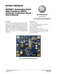
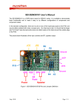
NCL30085FLYGEVB,
NCL30088FLYGEVB
10 W High Power Factor
Isolated LED Driver
Evaluation Board
User'sManual
www.onsemi.com
EVAL BOARD USER’S MANUAL
Overview
This manual covers the specification, theory of operation,
testing and construction of the NCL30085/88FLYGEVB
evaluation board. The NCL30085/88 board demonstrates a
10 W high PF isolated flyback LED driver in a typical A19
outline. The 2 evaluation boards are nearly identical in
construction except for the controller and Vcc bulk
capacitor. The NCL30088 controller is a non−dimming
version while the NCL30085 supports 3 levels of step
dimming.
Table 1. SPECIFICATIONS
Key Features
As illustrated, the key features of this evaluation board
include:
• Wide Mains
• Low THD across Line and Load
• High Power Factor across Wide Line and Load
• Integrated Auto Recovery Fault Protection (can be
latched by Choice A Version)
♦ Programmable Over Temperature Thermal Foldback
(NTC mounted on PCB)
♦ Cycle by Cycle Current Limiting
♦ Open LED and Shorted Output Protection
Parameter
Value
Input voltage (Class 2 Input,
no ground)
90 − 265 V ac
Line Frequency
50 Hz / 60 Hz
Power Factor (100% Load)
THD (100% Load)
Comment
0.9
Min
20%
Max
Class 2 Output Mains
Isolated
Output Voltage Range
Output Current
Efficiency
Start Up Time
EMI (conducted)
14 − 28 V dc
350 mA dc
±2%
85%
Typical
< 500 msec
Typical
Class B
FCC/CISPR
Figure 1. Evaluation Board Picture (Top View)
© Semiconductor Components Industries, LLC, 2014
December, 2014 − Rev. 0
1
Publication Order Number:
EVBUM2287/D
NCL30088FLYGEVB
THEORY OF OPERATION
Power Stage
Auxiliary Winding
The power stage for the evaluation boards is an isolated
flyback. The controller has a built in control algorithm that
is specific to the flyback transfer function. Specifically:
The auxiliary winding has 3 functions:
1. CrM timing
2. Vcc Power
3. Output voltage sense
Vout + Duty
(1*Duty)
Vin
CrM Timing
In the off time, the voltage on the transformer/inductor
forward biases Dout and D9. When the current in the
magnetic has reached zero, the voltage collapses to zero.
This voltage collapse triggers a comparator on the ZCD pin
to start a new switching cycle. The ZCD pin also counts rings
on the auxiliary winding for higher order valley operation.
A failure of the ZCD pin to reach a certain threshold also
indicates a shorted output condition fault.
This is applicable to flyback, buck boost, and SEPIC
converters. The control is very similar to the control of the
NCL30080−83 with the addition of a power factor
correction control loop. The controller has a built in
hardware algorithm that relates the output current to a
reference on the primary side.
Iout +
Vref Nps
2 Rsense
Nps +
Npri
Nsec
Vcc Power
The forward biases D9 to provide power for the controller.
This arrangement is called a “bootstrap”. Initially the Cvcc,
is charged through R4 and R5. When the voltage on Cvcc
reaches the startup threshold, the controller starts switching
and providing power to the output circuit and the Cvcc. Cvcc
discharges as the controller draws current. As the output
voltage rises, the auxiliary winding starts to provide all the
power to the controller. Ideally, this happens before Cvcc
discharges to the undervoltage threshold where the
controller stops operating to allow Cvcc to recharge once
again. The size of the output capacitor will have a large
effect on the rise of the output voltage. Since the LED driver
is a current source, the rise of output voltage is directly
dependent on the size of the output capacitor.
There are tradeoffs in the selection of Cout and Cvcc. A
low output ripple will require a large Cout value. This
requires that Cvcc be large enough to support Vcc power to
the controller while Cout is charging up. A large value of
Cvcc requires that R4 and R5 be lower in value to allow a fast
enough startup time. Smaller values of R4 and R5 have
higher static power dissipation which lowers efficiency of
the driver.
Where Npri = Primary Turns and Nsec = Secondary Turns
We can now find Rsense for a given output current.
Rsense +
Vref Nps
2 Iout
Line Feedforward
R3 sets the line feedforward which compensates for
power stage delay times by reducing the current threshold as
the line voltage increases. R3 is also used by the shorted pin
detection. At start up the controller generates a current from
the CS pin to check for a short to ground. If R3 is zero, the
current sense resistor is too low a value and the controller
will not start because it will detect a shorted pin. So R3 is
required to make the controller operate properly.
Voltage Sense
The voltage sense pin has several functions:
1. Basis for the reference of the PFC control loop
2. Line Range detection
The reference scaling is automatically controller inside
the controller. While the voltage on Vs is not critical for the
PFC loop control it is important for range detection.
Generally the voltage on Vs should be 3.5 V peak at the
highest input voltage of interest. The voltage on Vs
determines which valley the power stage will operate at in
full load. At low line and maximum load, the power stage
operates in the first valley (standard CrM operation). At the
higher line range, the power stage moves to the second
valley to lower the switching frequency while retaining the
advantage of CrM soft switching.
Output Voltage Sense
The auxiliary winding voltage is proportional to the
output voltage by the turns ratio of the output winding and
the auxiliary winding. The controller has an overvoltage
limit on the Vcc pin at about 26 V minimum. Above that
threshold, the controller will stop operation and enter a fault
mode for overvoltage. This is the open load protection.
In cases where the output has a lot of ripple current and the
LED has high dynamic resistance, the peak output voltage
can be much higher than the average output voltage. The
auxiliary winding will charge the Cvcc to the peak of the
output voltage which may trigger the OVP sooner than
expected.
www.onsemi.com
2
NCL30088FLYGEVB
SD Pin
Step Dimming
The SD pin is a multifunction protection input.
1. Thermal Foldback Protection
2. Programmable OVP
Step dimming is only available on the
NCL30085FLYGEVB. Cbulk is added to keep Vcc active
for brief AC power interruptions. There are 3 dimming
current levels for the NCL30085FLYGEVB after the driver
is powered on.
ON 100%
1.
70%
2.
25%
3.
4%
AC power interruption is detected on Vs when the voltage
on Vs is below 1 V for 30 ms. Internally, the controller steps
the internal Vref down to the next dimming level. After the
lowest level, Vref cycles back to 100%. Issues with step
dimming can be traced to Vcc dropping below the
undervoltage cutoff before the input has been detected as off
for 35 ms minimum.. This is caused by one of the following:
1. Operating Vcc too low (related to Vled)
2. Cbulk too small
3. Cout too large and discharges too much during the
AC interruption. This is particularly seen at the
lowest dim levels where the output current cannot
recharge Cout fast enough.
For a more detailed discussion of step dimming, refer to
DN05065/D.
Thermal Foldback
The OCV of the SD pin is 1.35 V. There is an internal
current source connected to the SD pin even though the
voltage is soft clamped to 1.35 V. Output current is reduced
when the voltage on the SD pin drops below 1 V. Placing an
NTC on the SD pin will allow the designer to choose the
level of protection from over temperature. Below 0.5 volts
on SD, the controller stops. Series or parallel resistors on the
NTC can shape the foldback curve. An online EXCEL®
based design tool is available at onsemi.com which provides
support to select the appropriate value.
Programmable OVP
While the SD pin has a current source for the OTP, it can
be overcome raising the voltage on the SD pin. At about
2.75 V, the SD pin detects an OVP and shuts down the
controller. Typically, a zener to Vcc is used for this. In this
way, the designer can set the OVP to a lower value that the
OVP threshold built into the Vcc pin.
Circuit Modifications
Output Current
The output current is set by the value of Rsense as shown
above. It’s possible to adjust easily change the output current
within ±10% of the set value by changing R7. Further
adjustments may require changes to the transformer
depending on the LED VF and current.
www.onsemi.com
3
NCL30088FLYGEVB
SCHEMATIC
+HVDC
R10
L3
+HVDC_iso
1.5mH
10k
1
AC_L
AC_N
F1
L2
FUSE
2.7mH
L1
1
C4
D4
AC1
+
AC2
−
C5
120nF 400V
120nF 400V
MB6S
2.7mH
R11
10k
Figure 2. Input Circuit
Cbulk is not stuffed on the NCL30088 version.
R4
+HVDC
R5
75k
T1
+HVDC_iso
75k
Rclmp
D9
Dout
MURA220T3
100k
BAS21DW5T1G
LED+
1
Rpre
20k
C14
620k
CVcc
Cbulk
4.7 mF
27 mF
470p 250VAC Y2
Dclmp
C15
UFM15PL
470p 250VAC Y2
Rzcd
56k
8
U1
ZCD
2
Vs
3
Comp
4
SD
Rtco
1n
C10
1 mF
Vcc
1
7
Q1
Com
GDrv
NDD02N60Z
CS
5
C13
R3
6
C12
R2
330uF 35V
1
R6
10k
Cout
t
1000p 630V
820
NCL30085/8
100 kW NTC
R7
16
Figure 3. Main Schematic
www.onsemi.com
4
Rsens
1.43
LED−
NCL30088FLYGEVB
BILL OF MATERIAL
Table 2. BILL OF MATERIAL*
Qty
Reference
Part
Manufacturer
Mfr_PN
PCB Footprint
Substitution
Allowed
1
Cvcc
4.7 mF
AVX
TAJB475M035RNJ
1210
Yes
1
Cbulk
27 mF
Panasonic
EEU−FC1E270
CAP−ALEL−4X11−
HOR
Yes
1
Cout
330 mF 35 V
Nichicon
UHE1V331MPD
CAP−ALEL−10X16
−HOR
Yes
2
C4, C5
120 nF 400 V
Epcos
B32559C6124+***
CAP−BOX−LS5−
5M0X7M2
Yes
1
C10
1 mF
Taiyo Yuden
GMK107AB7105KAHT
603
Yes
1
C12
1n
Kemet
C0402C102K3GACTU
402
Yes
1
C13
1000 p 630 V
Kemet
C0805C102KBRACTU
805
Yes
2
C14, C15
470 p 250 VAC Y2
Murata
GA342QR7GF471KW01L
1808
Yes
1
Dclmp
UFM15PL
MCC
UFM15PL
SOD123FL
Yes
1
Dout
MURA220T3
ON Semiconductor
MURA220T3
SMA
No
1
D4
MB6S
MCC
MB6S
MB6S
Yes
1
D9
BAS21DW5T1G
ON Semiconductor
BAS21DW5T1G
SC−88A
No
1
F1
FUSE
Littelfuse
0263.500WRT1L
FUSE−HAIRPIN−
LS250
Yes
2
L1, L2
2.7 mH
Bourns
RL875S−272K
Drum_Core_Hor_
LS5_875S
Yes
1
L3
1.5 mH
Wurth
7447462152
IND−UPRIGHT−
LS25
Yes
1
Q1
NDD02N60Z
ON Semiconductor
NDD02N60Z
IPAK
No
1
Rclmp
100 k
Yaego
RC1206FR−07100KL
1206
Yes
1
Rpre
20 k
Yaego
RC0603FR−0720KL
603
Yes
1
Rsens
1.43
Yaego
RC1206FR−071R43L
1206
Yes
1
Rtco
100 kW NTC
Epcos
B57331V2104J60
603
Yes
1
Rzcd
56k
Yaego
RC0805FR−0756KL
805
Yes
1
R2
10k
Yaego
RC0402FR−0710KL
402
Yes
1
R3
820
Yaego
RC0402FR−07820RL
402
Yes
2
R4, R5
75 k
Yaego
RC1206FR−0775KL
1206
Yes
1
R6
620 k
Yaego
RC1206FR−07620KL
1206
Yes
1
R7
16
Yaego
RT0402FRE0716RL
603
Yes
2
R10, R11
10 k
Yaego
RC0805JR−0710KL
805
Yes
1
T1
XFRM_LINEAR
Wurth
7508112342
RM6−4P−TH−
FLYLEADS
Yes
1
U1
NCL30085B
ON Semiconductor
NCL30085B
SO8
No
NCL30088B
NCL30088B
6”
W1
Wire, Red, 24AWG
McMaster Carr
7587K922
UL1569
Yes
6”
W2
Wire, Blk, 24AWG
McMaster Carr
7587K921
UL1569
Yes
12”
W3, W4
Wire, Wht, 24AWG
McMaster Carr
7587K924
UL1569
Yes
*All Components to comply with RoHS 2002/95/EC
www.onsemi.com
5
NCL30088FLYGEVB
GERBER VIEWS
Figure 4. Top Side PCB
Figure 5. Bottom Side PCB
Figure 6. PCB Outline
www.onsemi.com
6
NCL30088FLYGEVB
Mark the appropriate Version Here
White Wires Here
Cbulk not stuffed on NCL30088FLYGEVB
Short Flying Lead Here
Black Wire Here
Long Flying Lead Here
1. Trim Transformer flying leads for minimum length.
2. Strip and tin lead wires to 6” ± 0.5” 4 Places.
Figure 7. Assembly Notes
www.onsemi.com
7
Red Wire Here
NCL30088FLYGEVB
CIRCUIT BOARD FABRICATION NOTES
11. Size tolerance of plated holes: ±0.003 in. :
non−plated holes ±0.002 in.
12. All holes shall be ±0.003 in. of their true position
U.D.S.
13. Construction to be SMOBC, using liquid photo
image (LPI) solder mask in accordance with
IPC−SM−B40C, Type B, Class 2, and be green in
color.
14. Solder mask mis-registration ±0.004 in. max.
15. Silkscreen shall be permanent non−conductive
white ink.
16. The fabrication process shall be UL approved and
the PCB shall have a flammability rating of
UL94V0 to be marked on the solder side in
silkscreen with date, manufactures approved logo,
and type designation.
17. Warp and twist of the PCB shall not exceed
0.0075 in. per in.
18. 100% electrical verification required.
19. Surface finish: electroless nickel immersion gold
(ENIG)
20. RoHS 2002/95/EC compliance required.
1. Fabricate per IPC−6011 and IPC6012. Inspect to
IPA−A−600 Class 2 or updated standard.
2. Printed Circuit Board is defined by files listed in
fileset.
3. Modification to copper within the PCB outline is
not allowed without permission, except where
noted otherwise. The manufacturer may make
adjustments to compensate for manufacturing
process, but the final PCB is required to reflect the
associated gerber file design ±0.001 in. for etched
features within the PCB outline.
4. Material in accordance with IPC−4101/21, FR4,
Tg 125°C min.
5. Layer to layer registration shall not exceed
±0.004 in.
6. External finished copper conductor thickness shall
be 0.0026 in. min. (ie 2oz)
7. Copper plating thickness for through holes shall be
0.0013 in. min. (ie 1oz)
8. All holes sizes are finished hole size.
9. Finished PCB thickness 0.031 in.
10. All un-dimensioned holes to be drilled using the
NC drill data.
www.onsemi.com
8
NCL30088FLYGEVB
FLYBACK TRANSFORMER SPECIFICATION
www.onsemi.com
9
NCL30088FLYGEVB
ECA PICTURES
Figure 8. Top View
Figure 9. Bottom View
www.onsemi.com
10
NCL30088FLYGEVB
TEST PROCEDURE
Equipment Needed
Test Connections
• AC Source – 90 to 305 V ac 50/60 Hz Minimum 500 W
•
•
•
•
1. Connect the LED Load to the red (+) and black (−)
leads through the ammeter shown in Figure 10.
CAUTION: Observe the correct polarity or the load may
be damaged.
2. Connect the AC power to the input of the AC
wattmeter shown in Figure 10. Connect the white
leads to the output of the AC wattmeter
3. Connect the DC voltmeter as shown in Figure 10.
capability
AC Wattmeter – 300 W Minimum, True RMS Input
Voltage, Current, Power Factor, and THD 0.2%
accuracy or better
DC Voltmeter – 300 V dc minimum 0.1% accuracy or
better
DC Ammeter – 1 A dc minimum 0.1% accuracy or
better
LED Load – 10 V – 30 V @ 1 A
AC Power
AC
Source
Wattmeter
UUT
DC Ammeter
DC Voltmeter
LED Test
Load
NOTE: Unless otherwise specified, all voltage measurements are taken at the terminals of the UUT.
Figure 10. Test Set Up
Functional Test Procedure
1. Set the LED Load for 26 V output.
2. Set the input power to 120 V 60 Hz.
CAUTION: Do not touch the ECA once it is energized
because there are hazardous voltages
present.
LINE AND LOAD REGULATION
Table 3. 120 V / MAX LOAD
Output Current
350 mA + 14 mA
Output Power
Power Factor
THD < 20%
Output Power
Power Factor
THD < 30%
14 V
21 V
28 V
Table 4. 230 V / MAX LOAD
Output Current
350 mA + 14 mA
14 V
21 V
28 V
Efficiency + Vout Iout
Pin
100%
www.onsemi.com
11
NCL30088FLYGEVB
TEST DATA
Figure 11. Power Factor over Line and Load
Figure 12. THD over Line and Load
www.onsemi.com
12
NCL30088FLYGEVB
Figure 13. Efficiency over Line and Load at Maximum Output Current
Figure 14. Maximum Current Load Regulation over Line
www.onsemi.com
13
NCL30088FLYGEVB
Figure 15. 70% Load Regulation over Line (NCL30085FLYG only)
Figure 16. 25% Load Regulation over Line (NCL30085FLYG only)
www.onsemi.com
14
NCL30088FLYGEVB
Figure 17. Minimum Load Regulation over Line (NCL30085FLYG only)
Figure 18. Start Up with AC Applied 120 V Maximum Load
www.onsemi.com
15
NCL30088FLYGEVB
Figure 19. Start Up with AC Applied 230 V Maximum Load
Figure 20. Conducted EMI Pre−compliance QP Data 150 kHz − 1 MHz
www.onsemi.com
16
NCL30088FLYGEVB
Figure 21. Conducted EMI Pre−compliance Peak Data 150 kHz − 30 MHz
Excel is a registered trademark of Microsoft Corporation.
ON Semiconductor and the
are registered trademarks of Semiconductor Components Industries, LLC (SCILLC) or its subsidiaries in the United States and/or other countries.
SCILLC owns the rights to a number of patents, trademarks, copyrights, trade secrets, and other intellectual property. A listing of SCILLC’s product/patent coverage may be accessed
at www.onsemi.com/site/pdf/Patent−Marking.pdf. SCILLC reserves the right to make changes without further notice to any products herein. SCILLC makes no warranty, representation
or guarantee regarding the suitability of its products for any particular purpose, nor does SCILLC assume any liability arising out of the application or use of any product or circuit, and
specifically disclaims any and all liability, including without limitation special, consequential or incidental damages. “Typical” parameters which may be provided in SCILLC data sheets
and/or specifications can and do vary in different applications and actual performance may vary over time. All operating parameters, including “Typicals” must be validated for each
customer application by customer’s technical experts. SCILLC does not convey any license under its patent rights nor the rights of others. SCILLC products are not designed, intended,
or authorized for use as components in systems intended for surgical implant into the body, or other applications intended to support or sustain life, or for any other application in which
the failure of the SCILLC product could create a situation where personal injury or death may occur. Should Buyer purchase or use SCILLC products for any such unintended or
unauthorized application, Buyer shall indemnify and hold SCILLC and its officers, employees, subsidiaries, affiliates, and distributors harmless against all claims, costs, damages, and
expenses, and reasonable attorney fees arising out of, directly or indirectly, any claim of personal injury or death associated with such unintended or unauthorized use, even if such claim
alleges that SCILLC was negligent regarding the design or manufacture of the part. SCILLC is an Equal Opportunity/Affirmative Action Employer. This literature is subject to all applicable
copyright laws and is not for resale in any manner.
PUBLICATION ORDERING INFORMATION
LITERATURE FULFILLMENT:
Literature Distribution Center for ON Semiconductor
P.O. Box 5163, Denver, Colorado 80217 USA
Phone: 303−675−2175 or 800−344−3860 Toll Free USA/Canada
Fax: 303−675−2176 or 800−344−3867 Toll Free USA/Canada
Email: [email protected]
N. American Technical Support: 800−282−9855 Toll Free
USA/Canada
Europe, Middle East and Africa Technical Support:
Phone: 421 33 790 2910
Japan Customer Focus Center
Phone: 81−3−5817−1050
www.onsemi.com
17
ON Semiconductor Website: www.onsemi.com
Order Literature: http://www.onsemi.com/orderlit
For additional information, please contact your local
Sales Representative
EVBUM2287/D