1
LPC1850/30/20/10
32-bit ARM Cortex-M3 flashless MCU; up to 200 kB SRAM;
Ethernet, two HS USB, LCD, and external memory controller
Rev. 6.6 — 16 November 2015
Product data sheet
1. General description
The LPC1850/30/20/10 are ARM Cortex-M3 based microcontrollers for embedded
applications. The ARM Cortex-M3 is a next generation core that offers system
enhancements such as low power consumption, enhanced debug features, and a high
level of support block integration.
The LPC1850/30/20/10 operate at CPU frequencies of up to 180 MHz. The ARM
Cortex-M3 CPU incorporates a 3-stage pipeline and uses a Harvard architecture with
separate local instruction and data buses as well as a third bus for peripherals. The ARM
Cortex-M3 CPU also includes an internal prefetch unit that supports speculative
branching.
The LPC1850/30/20/10 include up to 200 kB of on-chip SRAM, a quad SPI Flash
Interface (SPIFI), a State Configurable Timer/PWM (SCTimer/PWM) subsystem, two
High-speed USB controllers, Ethernet, LCD, an external memory controller, and multiple
digital and analog peripherals.
See Section 17 “References” for additional documentation.
2. Features and benefits
Processor core
ARM Cortex-M3 processor (version r2p1), running at frequencies of up to
180 MHz.
ARM Cortex-M3 built-in Memory Protection Unit (MPU) supporting eight regions.
ARM Cortex-M3 built-in Nested Vectored Interrupt Controller (NVIC).
Non-maskable Interrupt (NMI) input.
JTAG and Serial Wire Debug, serial trace, eight breakpoints, and four watch points.
Enhanced Trace Module (ETM) and Enhanced Trace Buffer (ETB) support.
System tick timer.
On-chip memory
200 kB SRAM for code and data use.
Multiple SRAM blocks with separate bus access.
64 kB ROM containing boot code and on-chip software drivers.
64 bit + 256 bit One-Time Programmable (OTP) memory for general-purpose use.
Clock generation unit
Crystal oscillator with an operating range of 1 MHz to 25 MHz.
12 MHz internal RC oscillator trimmed to 1.5 % accuracy over temperature and
voltage.
LPC1850/30/20/10
NXP Semiconductors
32-bit ARM Cortex-M3 microcontroller
Ultra-low power RTC crystal oscillator.
Three PLLs allow CPU operation up to the maximum CPU rate without the need for
a high-frequency crystal. The second PLL is dedicated to the High-speed USB, the
third PLL can be used as audio PLL.
Clock output.
Configurable digital peripherals:
State Configurable Timer (SCTimer/PWM) subsystem on AHB.
Global Input Multiplexer Array (GIMA) allows to cross-connect multiple inputs and
outputs to event driven peripherals like timers, SCTimer/PWM, and ADC0/1.
Serial interfaces:
Quad SPI Flash Interface (SPIFI) with 1-, 2-, or 4-bit data at rates of up to
52 MB per second.
10/100T Ethernet MAC with RMII and MII interfaces and DMA support for high
throughput at low CPU load. Support for IEEE 1588 time stamping/advanced time
stamping (IEEE 1588-2008 v2).
One High-speed USB 2.0 Host/Device/OTG interface with DMA support and
on-chip high-speed PHY (USB0).
One High-speed USB 2.0 Host/Device interface with DMA support, on-chip
full-speed PHY and ULPI interface to an external high-speed PHY (USB1).
USB interface electrical test software included in ROM USB stack.
Four 550 UARTs with DMA support: one UART with full modem interface; one
UART with IrDA interface; three USARTs support UART synchronous mode and a
smart card interface conforming to ISO7816 specification.
Up to two C_CAN 2.0B controllers with one channel each. Use of C_CAN controller
excludes operation of all other peripherals connected to the same bus bridge See
Figure 1 and Ref. 2.
Two SSP controllers with FIFO and multi-protocol support. Both SSPs with DMA
support.
One Fast-mode Plus I2C-bus interface with monitor mode and with open-drain I/O
pins conforming to the full I2C-bus specification. Supports data rates of up to
1 Mbit/s.
One standard I2C-bus interface with monitor mode and standard I/O pins.
Two I2S interfaces with DMA support, each with one input and one output.
Digital peripherals:
External Memory Controller (EMC) supporting external SRAM, ROM, NOR flash,
and SDRAM devices.
LCD controller with DMA support and a programmable display resolution of up to
1024 H 768 V. Supports monochrome and color STN panels and TFT color
panels; supports 1/2/4/8 bpp Color Look-Up Table (CLUT) and 16/24-bit direct pixel
mapping.
Secure Digital Input Output (SD/MMC) card interface.
Eight-channel General-Purpose DMA controller can access all memories on the
AHB and all DMA-capable AHB slaves.
Up to 164 General-Purpose Input/Output (GPIO) pins with configurable
pull-up/pull-down resistors.
GPIO registers are located on the AHB for fast access. GPIO ports have DMA
support.
LPC1850_30_20_10
Product data sheet
All information provided in this document is subject to legal disclaimers.
Rev. 6.6 — 16 November 2015
© NXP Semiconductors N.V. 2015. All rights reserved.
2 of 153
LPC1850/30/20/10
NXP Semiconductors
32-bit ARM Cortex-M3 microcontroller
Up to eight GPIO pins can be selected from all GPIO pins as edge and level
sensitive interrupt sources.
Two GPIO group interrupt modules enable an interrupt based on a programmable
pattern of input states of a group of GPIO pins.
Four general-purpose timer/counters with capture and match capabilities.
One motor control PWM for three-phase motor control.
One Quadrature Encoder Interface (QEI).
Repetitive Interrupt timer (RI timer).
Windowed watchdog timer.
Ultra-low power Real-Time Clock (RTC) on separate power domain with 256 bytes
of battery powered backup registers.
Alarm timer; can be battery powered.
Analog peripherals:
One 10-bit DAC with DMA support and a data conversion rate of 400 kSamples/s.
Two 10-bit ADCs with DMA support and a data conversion rate of 400 kSamples/s.
Up to eight input channels per ADC.
Unique ID for each device.
Power:
Single 3.3 V (2.2 V to 3.6 V) power supply with on-chip internal voltage regulator for
the core supply and the RTC power domain.
RTC power domain can be powered separately by a 3 V battery supply.
Four reduced power modes: Sleep, Deep-sleep, Power-down, and Deep
power-down.
Processor wake-up from Sleep mode via wake-up interrupts from various
peripherals.
Wake-up from Deep-sleep, Power-down, and Deep power-down modes via
external interrupts and interrupts generated by battery powered blocks in the RTC
power domain.
Brownout detect with four separate thresholds for interrupt and forced reset.
Power-On Reset (POR).
Available as 144-pin LQFP packages and as 256-pin, 180-pin, and 100-pin BGA
packages.
3. Applications
Industrial
Consumer
White goods
LPC1850_30_20_10
Product data sheet
RFID readers
e-Metering
All information provided in this document is subject to legal disclaimers.
Rev. 6.6 — 16 November 2015
© NXP Semiconductors N.V. 2015. All rights reserved.
3 of 153
LPC1850/30/20/10
NXP Semiconductors
32-bit ARM Cortex-M3 microcontroller
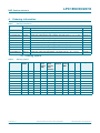
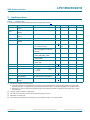
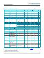
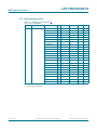
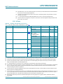
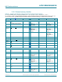
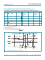
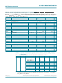
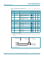
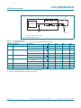
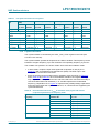
4. Ordering information
Table 1.
Ordering information
Type number
LPC1850FET256
Package
Name
Description
Version
LBGA256
Plastic low profile ball grid array package; 256 balls; body 17 17 1 mm
SOT740-2
LPC1850FET180
TFBGA180 Thin fine-pitch ball grid array package; 180 balls
LPC1830FET256
LBGA256
LPC1830FET180
TFBGA180 Thin fine-pitch ball grid array package; 180 balls
LPC1830FET100
TFBGA100 Plastic thin fine-pitch ball grid array package; 100 balls; body 9 9 0.7 mm SOT926-1
SOT486-1
TFBGA100 Plastic thin fine-pitch ball grid array package; 100 balls; body 9 9 0.7 mm SOT926-1
Plastic low profile quad flat package; 144 leads; body 20 20 1.4 mm
LPC1820FBD144 LQFP144
LPC1810FET100
SOT740-2
SOT570-3
Plastic low profile quad flat package; 144 leads; body 20 20 1.4 mm
LPC1830FBD144 LQFP144
LPC1820FET100
SOT570-3
Plastic low profile ball grid array package; 256 balls; body 17 17 1 mm
SOT486-1
TFBGA100 Plastic thin fine-pitch ball grid array package; 100 balls; body 9 9 0.7 mm SOT926-1
Plastic low profile quad flat package; 144 leads; body 20 20 1.4 mm
LPC1810FBD144 LQFP144
SOT486-1
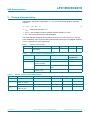
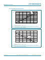
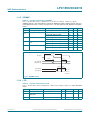
4.1 Ordering options
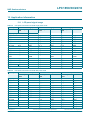
Table 2.
Ordering options
Type number
Total
SRAM
LCD Ethernet USB0
(Host,
Device,
OTG)
USB1
ADC
Motor QEI
(Host,
channels control
Device)/
PWM
ULPI
interface
GPIO
Package
LPC1850FET256 200 kB
yes
yes
yes
yes/yes
8
yes
yes
164
LBGA256
LPC1850FET180 200 kB
yes
yes
yes
yes/yes
8
yes
yes
118
TFBGA180
LPC1830FET256 200 kB
no
yes
yes
yes/yes
8
yes
yes
164
LBGA256
LPC1830FET180 200 kB
no
yes
yes
yes/yes
8
yes
yes
118
TFBGA180
LPC1830FET100 200 kB
no
yes
yes
yes/no
4
no
no
49
TFBGA100
LPC1830FBD144 200 kB
no
yes
yes
yes/no
8
yes
no
83
LQFP144
LPC1820FET100 168 kB
no
no
yes
no
4
no
no
49
TFBGA100
LPC1820FBD144 168 kB
no
no
yes
no
8
yes
no
83
LQFP144
LPC1810FET100 136 kB
no
no
no
no
4
no
no
49
TFBGA100
LPC1810FBD144 136 kB
no
no
no
no
8
yes
no
83
LQFP144
LPC1850_30_20_10
Product data sheet
All information provided in this document is subject to legal disclaimers.
Rev. 6.6 — 16 November 2015
© NXP Semiconductors N.V. 2015. All rights reserved.
4 of 153
LPC1850/30/20/10
NXP Semiconductors
32-bit ARM Cortex-M3 microcontroller
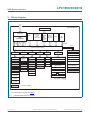
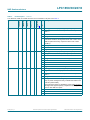
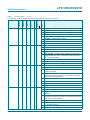
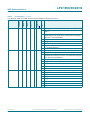
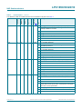
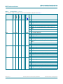
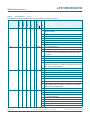
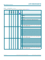
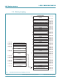
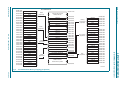
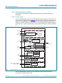
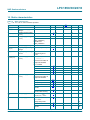
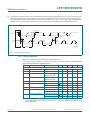
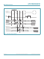
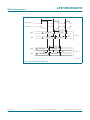
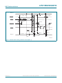
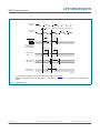
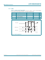
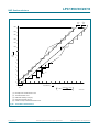
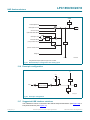
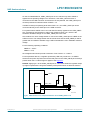
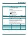
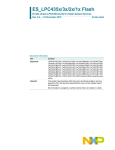
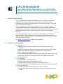
5. Block diagram
SWD/TRACE PORT/JTAG
LPC1850/30/20/10
HIGH-SPEED PHY
TEST/DEBUG
INTERFACE
ETHERNET(1)
10/100
MAC
IEEE 1588
DMA
ARM
CORTEX-M3
HIGHSPEED
USB0(1)
HOST/
DEVICE/
OTG
USB1(1)
HOST/
DEVICE
LCD(1)
SD/
MMC
system
bus
D-code
bus
I-code
bus
masters
slaves
AHB MULTILAYER MATRIX
SPIFI
slaves
BRIDGE 0
BRIDGE 1
BRIDGE 2
BRIDGE 3
BRIDGE
BRIDGE
RI TIMER
CGU
ALARM TIMER
64/96 kB LOCAL SRAM
USART0
MOTOR
CONTROL
PWM(1)
I2C1
USART2
10-bit DAC
CCU1
BACKUP REGISTERS
40 kB LOCAL SRAM
UART1
I2C0
USART3
C_CAN0
CCU2
POWER MODE CONTROL
16/32 kB AHB SRAM
SSP0
I2S0
TIMER2
10-bit ADC0
RGU
16 kB +
16 kB AHB SRAM(1)
TIMER0
I2S1
CONFIGURATION
REGISTERS
TIMER3
10-bit ADC1
EVENT ROUTER
HS GPIO
TIMER1
C_CAN1
SSP1
OTP MEMORY
SCT
EMC
64 kB ROM
WWDT
SCU
GPIO
interrupts
QEI(1)
RTC
RTC OSC
GIMA
12 MHz IRC
GPIO GROUP0
interrupt
RTC POWER DOMAIN
GPIO GROUP1
interrupt
= connected to GPDMA
002aaf218
(1) Not available on all parts (see Table 2).
Fig 1.
LPC1850/30/20/10 block diagram
LPC1850_30_20_10
Product data sheet
All information provided in this document is subject to legal disclaimers.
Rev. 6.6 — 16 November 2015
© NXP Semiconductors N.V. 2015. All rights reserved.
5 of 153
LPC1850/30/20/10
NXP Semiconductors
32-bit ARM Cortex-M3 microcontroller
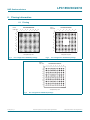
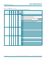
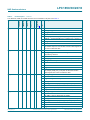
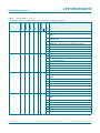
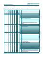
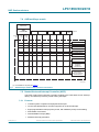
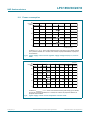
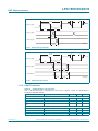
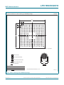
6. Pinning information
6.1 Pinning
LPC1850/30FET256
ball A1
index area
2
1
4
3
6
5
8
7
10
9
12
11
14
13
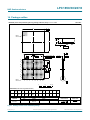
LPC1850/30FET180
ball A1
index area
16
2
1
15
A
4
3
6
5
8
7
10
9
12
11
A
B
B
C
C
D
D
E
E
F
G
F
J
H
L
K
G
H
K
J
M
L
N
M
P
N
R
P
T
002aag365
002aaf230
Transparent top view
Transparent top view
Fig 2.
14
13
Pin configuration LBGA256 package
Fig 3.
ball A1
index area
Pin configuration TFBGA180 package
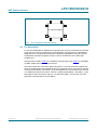
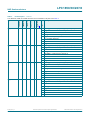
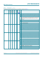
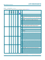
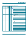
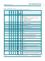
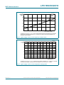
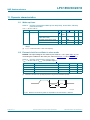
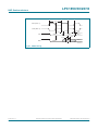
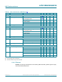
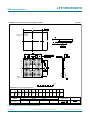
LPC1830/20/10FET100
1
2
3
4
5
6
7
8
9 10
A
B
C
D
E
F
G
H
J
K
002aag366
Transparent top view
Fig 4.
LPC1850_30_20_10
Product data sheet
Pin configuration TFBGA100 package
All information provided in this document is subject to legal disclaimers.
Rev. 6.6 — 16 November 2015
© NXP Semiconductors N.V. 2015. All rights reserved.
6 of 153
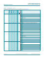
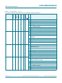
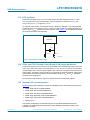
LPC1850/30/20/10
NXP Semiconductors
73
108
32-bit ARM Cortex-M3 microcontroller
109
72
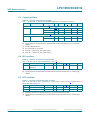
LPC1830/20/10FBD144
Fig 5.
36
37
1
144
002aag368
Pin configuration LQFP144 package
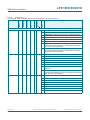
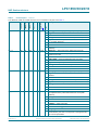
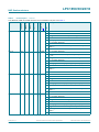
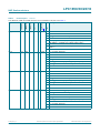
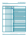
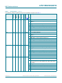
6.2 Pin description
On the LPC1850/30/20/10, digital pins are grouped into 16 ports, named P0 to P9 and PA
to PF, with up to 20 pins used per port. Each digital pin can support up to eight different
digital functions, including General-Purpose I/O (GPIO), selectable through the System
Configuration Unit (SCU) registers. The pin name is not indicative of the GPIO port
assigned to it.
Not all functions listed in Table 3 are available on all packages. See Table 2 for availability
of USB0, USB1, Ethernet, and LCD functions.
The parts contain two 10-bit ADCs (ADC0 and ADC1). The input channels of ADC0 and
ADC1 on dedicated pins and multiplexed pins are combined in such a way that all channel
0 inputs (named ADC0_0 and ADC1_0) are tied together and connected to both, channel
0 on ADC0 and channel 0 on ADC1, channel 1 inputs (named ADC0_1 and ADC1_1) are
tied together and connected to channel 1 on ADC0 and ADC1, and so forth. There are
eight ADC channels total for the two ADCs.
LPC1850_30_20_10
Product data sheet
All information provided in this document is subject to legal disclaimers.
Rev. 6.6 — 16 November 2015
© NXP Semiconductors N.V. 2015. All rights reserved.
7 of 153
LPC1850/30/20/10
NXP Semiconductors
32-bit ARM Cortex-M3 microcontroller
Type
32
Description
[1]
LQFP144
G2
Reset state
TFBGA100
LBGA256
Symbol
TFBGA180
Table 3.
Pin description
LCD, Ethernet, USB0, and USB1 functions are not available on all parts. See Table 2.
Multiplexed digital pins
P0_0
P0_1
L3
M2
K3
K2
G1
34
[2]
[2]
N; PU I/O
GPIO0[0] — General purpose digital input/output pin.
I/O
SSP1_MISO — Master In Slave Out for SSP1.
I
ENET_RXD1 — Ethernet receive data 1 (RMII/MII interface).
-
R — Function reserved.
-
R — Function reserved.
-
R — Function reserved.
I/O
I2S0_TX_WS — Transmit Word Select. It is driven by the
master and received by the slave. Corresponds to the signal
WS in the I2S-bus specification.
I/O
I2S1_TX_WS — Transmit Word Select. It is driven by the
master and received by the slave. Corresponds to the signal
WS in the I2S-bus specification.
N; PU I/O
GPIO0[1] — General purpose digital input/output pin.
I/O
SSP1_MOSI — Master Out Slave in for SSP1.
I
ENET_COL — Ethernet Collision detect (MII interface).
-
R — Function reserved.
-
R — Function reserved.
-
R — Function reserved.
ENET_TX_EN — Ethernet transmit enable (RMII/MII
interface).
I/O
P1_0
P2
LPC1850_30_20_10
Product data sheet
L1
H1
38
[2]
N; PU I/O
I2S1_TX_SDA — I2S1 transmit data. It is driven by the
transmitter and read by the receiver. Corresponds to the signal
SD in the I2S-bus specification.
GPIO0[4] — General purpose digital input/output pin.
I
CTIN_3 — SCTimer/PWM input 3. Capture input 1 of timer 1.
I/O
EMC_A5 — External memory address line 5.
-
R — Function reserved.
-
R — Function reserved.
I/O
SSP0_SSEL — Slave Select for SSP0.
-
R — Function reserved.
-
R — Function reserved.
All information provided in this document is subject to legal disclaimers.
Rev. 6.6 — 16 November 2015
© NXP Semiconductors N.V. 2015. All rights reserved.
8 of 153
LPC1850/30/20/10
NXP Semiconductors
32-bit ARM Cortex-M3 microcontroller
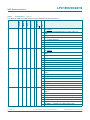
LQFP144
N1
K2
42
[2]
Type
TFBGA100
R2
Description
[1]
TFBGA180
P1_1
LBGA256
Symbol
Reset state
Table 3.
Pin description …continued
LCD, Ethernet, USB0, and USB1 functions are not available on all parts. See Table 2.
N; PU I/O
O
CTOUT_7 — SCTimer/PWM output 7. Match output 3 of
timer 1.
I/O
EMC_A6 — External memory address line 6.
-
R — Function reserved.
-
R — Function reserved.
I/O
SSP0_MISO — Master In Slave Out for SSP0.
-
R — Function reserved.
P1_2
P1_3
P1_4
R3
P5
T3
LPC1850_30_20_10
Product data sheet
N2
M2
P2
K1
J1
J2
43
44
47
[2]
[2]
[2]
GPIO0[8] — General purpose digital input/output pin. Boot pin
(see Table 5).
N; PU I/O
R — Function reserved.
GPIO0[9] — General purpose digital input/output pin. Boot pin
(see Table 5).
O
CTOUT_6 — SCTimer/PWM output 6. Match output 2 of
timer 1.
I/O
EMC_A7 — External memory address line 7.
-
R — Function reserved.
-
R — Function reserved.
I/O
SSP0_MOSI — Master Out Slave in for SSP0.
-
R — Function reserved.
-
R — Function reserved.
N; PU I/O
GPIO0[10] — General purpose digital input/output pin.
O
CTOUT_8 — SCTimer/PWM output 8. Match output 0 of
timer 2.
-
R — Function reserved.
O
EMC_OE — LOW active Output Enable signal.
O
USB0_IND1 — USB0 port indicator LED control output 1.
I/O
SSP1_MISO — Master In Slave Out for SSP1.
-
R — Function reserved.
O
SD_RST — SD/MMC reset signal for MMC4.4 card.
N; PU I/O
GPIO0[11] — General purpose digital input/output pin.
O
CTOUT_9 — SCTimer/PWM output 9. Match output 3 of
timer 3.
-
R — Function reserved.
O
EMC_BLS0 — LOW active Byte Lane select signal 0.
O
USB0_IND0 — USB0 port indicator LED control output 0.
I/O
SSP1_MOSI — Master Out Slave in for SSP1.
-
R — Function reserved.
O
SD_VOLT1 — SD/MMC bus voltage select output 1.
All information provided in this document is subject to legal disclaimers.
Rev. 6.6 — 16 November 2015
© NXP Semiconductors N.V. 2015. All rights reserved.
9 of 153
LPC1850/30/20/10
NXP Semiconductors
32-bit ARM Cortex-M3 microcontroller
P1_6
P1_7
LQFP144
N3
J4
48
T4
T5
P3
N4
K4
G4
49
50
[2]
[2]
[2]
Type
TFBGA100
R5
Description
[1]
TFBGA180
P1_5
LBGA256
Symbol
Reset state
Table 3.
Pin description …continued
LCD, Ethernet, USB0, and USB1 functions are not available on all parts. See Table 2.
N; PU I/O
GPIO1[8] — General purpose digital input/output pin.
O
CTOUT_10 — SCTimer/PWM output 10. Match output 3 of
timer 3.
-
R — Function reserved.
O
EMC_CS0 — LOW active Chip Select 0 signal.
I
USB0_PWR_FAULT — Port power fault signal indicating
overcurrent condition; this signal monitors over-current on the
USB bus (external circuitry required to detect over-current
condition).
I/O
SSP1_SSEL — Slave Select for SSP1.
-
R — Function reserved.
O
SD_POW — SD/MMC card power monitor output.
N; PU I/O
GPIO1[9] — General purpose digital input/output pin.
I
CTIN_5 — SCTimer/PWM input 5. Capture input 2 of timer 2.
-
R — Function reserved.
O
EMC_WE — LOW active Write Enable signal.
-
R — Function reserved.
-
R — Function reserved.
-
R — Function reserved.
I/O
SD_CMD — SD/MMC command signal.
N; PU I/O
GPIO1[0] — General purpose digital input/output pin.
I
U1_DSR — Data Set Ready input for UART1.
O
CTOUT_13 — SCTimer/PWM output 13. Match output 3 of
timer 3.
I/O
EMC_D0 — External memory data line 0.
O
USB0_PPWR — VBUS drive signal (towards external charge
pump or power management unit); indicates that VBUS must
be driven (active HIGH).
Add a pull-down resistor to disable the power switch at reset.
This signal has opposite polarity compared to the USB_PPWR
used on other NXP LPC parts.
LPC1850_30_20_10
Product data sheet
-
R — Function reserved.
-
R — Function reserved.
-
R — Function reserved.
All information provided in this document is subject to legal disclaimers.
Rev. 6.6 — 16 November 2015
© NXP Semiconductors N.V. 2015. All rights reserved.
10 of 153
LPC1850/30/20/10
NXP Semiconductors
32-bit ARM Cortex-M3 microcontroller
P1_9
LQFP144
M5
H5
51
T7
N5
J5
52
[2]
[2]
Type
TFBGA100
R7
Description
[1]
TFBGA180
P1_8
LBGA256
Symbol
Reset state
Table 3.
Pin description …continued
LCD, Ethernet, USB0, and USB1 functions are not available on all parts. See Table 2.
N; PU I/O
O
U1_DTR — Data Terminal Ready output for UART1.
O
CTOUT_12 — SCTimer/PWM output 12. Match output 3 of
timer 3.
I/O
EMC_D1 — External memory data line 1.
-
R — Function reserved.
-
R — Function reserved.
-
R — Function reserved.
O
SD_VOLT0 — SD/MMC bus voltage select output 0.
N; PU I/O
P1_11
R8
T9
LPC1850_30_20_10
Product data sheet
N6
P8
H6
J7
53
55
[2]
[2]
GPIO1[2] — General purpose digital input/output pin.
O
U1_RTS — Request to Send output for UART1.
O
CTOUT_11 — SCTimer/PWM output 11. Match output 3 of
timer 2.
I/O
EMC_D2 — External memory data line 2.
-
R — Function reserved.
-
R — Function reserved.
-
R — Function reserved.
I/O
P1_10
GPIO1[1] — General purpose digital input/output pin.
N; PU I/O
SD_DAT0 — SD/MMC data bus line 0.
GPIO1[3] — General purpose digital input/output pin.
I
U1_RI — Ring Indicator input for UART1.
O
CTOUT_14 — SCTimer/PWM output 14. Match output 2 of
timer 3.
I/O
EMC_D3 — External memory data line 3.
-
R — Function reserved.
-
R — Function reserved.
-
R — Function reserved.
I/O
SD_DAT1 — SD/MMC data bus line 1.
N; PU I/O
GPIO1[4] — General purpose digital input/output pin.
I
U1_CTS — Clear to Send input for UART1.
O
CTOUT_15 — SCTimer/PWM output 15. Match output 3 of
timer 3.
I/O
EMC_D4 — External memory data line 4.
-
R — Function reserved.
-
R — Function reserved.
-
R — Function reserved.
I/O
SD_DAT2 — SD/MMC data bus line 2.
All information provided in this document is subject to legal disclaimers.
Rev. 6.6 — 16 November 2015
© NXP Semiconductors N.V. 2015. All rights reserved.
11 of 153
LPC1850/30/20/10
NXP Semiconductors
32-bit ARM Cortex-M3 microcontroller
P1_13
P1_14
P1_15
LQFP144
P7
K7
56
R10
R11
T12
LPC1850_30_20_10
Product data sheet
L8
K7
P11
H8
J8
K8
60
61
62
[2]
[2]
[2]
[2]
Type
TFBGA100
R9
Description
[1]
TFBGA180
P1_12
LBGA256
Symbol
Reset state
Table 3.
Pin description …continued
LCD, Ethernet, USB0, and USB1 functions are not available on all parts. See Table 2.
N; PU I/O
GPIO1[5] — General purpose digital input/output pin.
I
U1_DCD — Data Carrier Detect input for UART1.
-
R — Function reserved.
I/O
EMC_D5 — External memory data line 5.
I
T0_CAP1 — Capture input 1 of timer 0.
-
R — Function reserved.
-
R — Function reserved.
I/O
SD_DAT3 — SD/MMC data bus line 3.
N; PU I/O
GPIO1[6] — General purpose digital input/output pin.
O
U1_TXD — Transmitter output for UART1.
-
R — Function reserved.
I/O
EMC_D6 — External memory data line 6.
I
T0_CAP0 — Capture input 0 of timer 0.
-
R — Function reserved.
-
R — Function reserved.
I
SD_CD — SD/MMC card detect input.
N; PU I/O
GPIO1[7] — General purpose digital input/output pin.
I
U1_RXD — Receiver input for UART1.
-
R — Function reserved.
I/O
EMC_D7 — External memory data line 7.
O
T0_MAT2 — Match output 2 of timer 0.
-
R — Function reserved.
-
R — Function reserved.
-
R — Function reserved.
N; PU I/O
GPIO0[2] — General purpose digital input/output pin.
O
U2_TXD — Transmitter output for USART2.
-
R — Function reserved.
I
ENET_RXD0 — Ethernet receive data 0 (RMII/MII interface).
O
T0_MAT1 — Match output 1 of timer 0.
-
R — Function reserved.
-
R — Function reserved.
-
R — Function reserved.
All information provided in this document is subject to legal disclaimers.
Rev. 6.6 — 16 November 2015
© NXP Semiconductors N.V. 2015. All rights reserved.
12 of 153
LPC1850/30/20/10
NXP Semiconductors
32-bit ARM Cortex-M3 microcontroller
P1_17
LQFP144
L5
H9
64
M8
L6
H10 66
[2]
[3]
Type
TFBGA100
M7
Description
[1]
TFBGA180
P1_16
LBGA256
Symbol
Reset state
Table 3.
Pin description …continued
LCD, Ethernet, USB0, and USB1 functions are not available on all parts. See Table 2.
N; PU I/O
I
U2_RXD — Receiver input for USART2.
-
R — Function reserved.
I
ENET_CRS — Ethernet Carrier Sense (MII interface).
O
T0_MAT0 — Match output 0 of timer 0.
-
R — Function reserved.
-
R — Function reserved.
I
ENET_RX_DV — Ethernet Receive Data Valid (RMII/MII
interface).
N; PU I/O
P1_19
N12
M11
LPC1850_30_20_10
Product data sheet
N10
N9
J10
K9
67
68
[2]
[2]
GPIO0[12] — General purpose digital input/output pin.
I/O
U2_UCLK — Serial clock input/output for USART2 in
synchronous mode.
-
R — Function reserved.
I/O
ENET_MDIO — Ethernet MIIM data input and output.
I
T0_CAP3 — Capture input 3 of timer 0.
O
CAN1_TD — CAN1 transmitter output.
-
R — Function reserved.
P1_18
GPIO0[3] — General purpose digital input/output pin.
N; PU I/O
R — Function reserved.
GPIO0[13] — General purpose digital input/output pin.
I/O
U2_DIR — RS-485/EIA-485 output enable/direction control for
USART2.
-
R — Function reserved.
O
ENET_TXD0 — Ethernet transmit data 0 (RMII/MII interface).
O
T0_MAT3 — Match output 3 of timer 0.
I
CAN1_RD — CAN1 receiver input.
-
R — Function reserved.
-
R — Function reserved.
N; PU I
ENET_TX_CLK (ENET_REF_CLK) — Ethernet Transmit
Clock (MII interface) or Ethernet Reference Clock (RMII
interface).
I/O
SSP1_SCK — Serial clock for SSP1.
-
R — Function reserved.
-
R — Function reserved.
O
CLKOUT — Clock output pin.
-
R — Function reserved.
O
I2S0_RX_MCLK — I2S receive master clock.
I/O
I2S1_TX_SCK — Transmit Clock. It is driven by the master
and received by the slave. Corresponds to the signal SCK in
the I2S-bus specification.
All information provided in this document is subject to legal disclaimers.
Rev. 6.6 — 16 November 2015
© NXP Semiconductors N.V. 2015. All rights reserved.
13 of 153
LPC1850/30/20/10
NXP Semiconductors
32-bit ARM Cortex-M3 microcontroller
P2_0
K10 70
T16
N14
G10 75
[2]
[2]
Type
J10
Description
[1]
TFBGA100
M10
LQFP144
TFBGA180
P1_20
LBGA256
Symbol
Reset state
Table 3.
Pin description …continued
LCD, Ethernet, USB0, and USB1 functions are not available on all parts. See Table 2.
N; PU I/O
GPIO0[15] — General purpose digital input/output pin.
I/O
SSP1_SSEL — Slave Select for SSP1.
-
R — Function reserved.
O
ENET_TXD1 — Ethernet transmit data 1 (RMII/MII interface).
I
T0_CAP2 — Capture input 2 of timer 0.
-
R — Function reserved.
-
R — Function reserved.
-
R — Function reserved.
N; PU -
R — Function reserved.
O
U0_TXD — Transmitter output for USART0.
I/O
EMC_A13 — External memory address line 13.
O
USB0_PPWR — VBUS drive signal (towards external charge
pump or power management unit); indicates that VBUS must
be driven (active high).
Add a pull-down resistor to disable the power switch at reset.
This signal has opposite polarity compared to the USB_PPWR
used on other NXP LPC parts.
I/O
GPIO5[0] — General purpose digital input/output pin.
-
R — Function reserved.
I
T3_CAP0 — Capture input 0 of timer 3.
O
P2_1
N15
LPC1850_30_20_10
Product data sheet
M13 G7
81
[2]
N; PU -
ENET_MDC — Ethernet MIIM clock.
R — Function reserved.
I
U0_RXD — Receiver input for USART0.
I/O
EMC_A12 — External memory address line 12.
I
USB0_PWR_FAULT — Port power fault signal indicating
overcurrent condition; this signal monitors over-current on the
USB bus (external circuitry required to detect over-current
condition).
I/O
GPIO5[1] — General purpose digital input/output pin.
-
R — Function reserved.
I
T3_CAP1 — Capture input 1 of timer 3.
-
R — Function reserved.
All information provided in this document is subject to legal disclaimers.
Rev. 6.6 — 16 November 2015
© NXP Semiconductors N.V. 2015. All rights reserved.
14 of 153
LPC1850/30/20/10
NXP Semiconductors
32-bit ARM Cortex-M3 microcontroller
P2_3
LQFP144
L13
F5
84
J12
G11
D8
87
[2]
[3]
Type
TFBGA100
M15
Description
[1]
TFBGA180
P2_2
LBGA256
Symbol
Reset state
Table 3.
Pin description …continued
LCD, Ethernet, USB0, and USB1 functions are not available on all parts. See Table 2.
N; PU -
R — Function reserved.
I/O
U0_UCLK — Serial clock input/output for USART0 in
synchronous mode.
I/O
EMC_A11 — External memory address line 11.
O
USB0_IND1 — USB0 port indicator LED control output 1.
I/O
GPIO5[2] — General purpose digital input/output pin.
I
CTIN_6 — SCTimer/PWM input 6. Capture input 1 of timer 3.
I
T3_CAP2 — Capture input 2 of timer 3.
-
R — Function reserved.
N; PU -
R — Function reserved.
I/O
I2C1_SDA — I2C1 data input/output (this pin does not use a
specialized I2C pad).
O
U3_TXD — Transmitter output for USART3.
I
CTIN_1 — SCTimer/PWM input 1. Capture input 1 of timer 0.
Capture input 1 of timer 2.
I/O
GPIO5[3] — General purpose digital input/output pin.
-
R — Function reserved.
O
T3_MAT0 — Match output 0 of timer 3.
O
USB0_PPWR — VBUS drive signal (towards external charge
pump or power management unit); indicates that VBUS must
be driven (active HIGH).
Add a pull-down resistor to disable the power switch at reset.
This signal has opposite polarity compared to the USB_PPWR
used on other NXP LPC parts.
P2_4
K11
LPC1850_30_20_10
Product data sheet
L9
D9
88
[3]
N; PU -
R — Function reserved.
I/O
I2C1_SCL — I2C1 clock input/output (this pin does not use a
specialized I2C pad).
I
U3_RXD — Receiver input for USART3.
I
CTIN_0 — SCTimer/PWM input 0. Capture input 0 of timer 0,
1, 2, 3.
I/O
GPIO5[4] — General purpose digital input/output pin.
-
R — Function reserved.
O
T3_MAT1 — Match output 1 of timer 3.
I
USB0_PWR_FAULT — Port power fault signal indicating
overcurrent condition; this signal monitors over-current on the
USB bus (external circuitry required to detect over-current
condition).
All information provided in this document is subject to legal disclaimers.
Rev. 6.6 — 16 November 2015
© NXP Semiconductors N.V. 2015. All rights reserved.
15 of 153
LPC1850/30/20/10
NXP Semiconductors
32-bit ARM Cortex-M3 microcontroller
D10 91
[3]
Type
J12
Description
[1]
TFBGA100
K14
LQFP144
TFBGA180
P2_5
LBGA256
Symbol
Reset state
Table 3.
Pin description …continued
LCD, Ethernet, USB0, and USB1 functions are not available on all parts. See Table 2.
N; PU -
R — Function reserved.
I
CTIN_2 — SCTimer/PWM input 2. Capture input 2 of timer 0.
I
USB1_VBUS — Monitors the presence of USB1 bus power.
Note: This signal must be HIGH for USB reset to occur.
P2_6
P2_7
K16
H14
LPC1850_30_20_10
Product data sheet
J14
G12
G9
95
C10 96
[2]
[2]
I
ADCTRIG1 — ADC trigger input 1.
I/O
GPIO5[5] — General purpose digital input/output pin.
-
R — Function reserved.
O
T3_MAT2 — Match output 2 of timer 3.
O
USB0_IND0 — USB0 port indicator LED control
output 0.
N; PU -
R — Function reserved.
I/O
U0_DIR — RS-485/EIA-485 output enable/direction control for
USART0.
I/O
EMC_A10 — External memory address line 10.
O
USB0_IND0 — USB0 port indicator LED control
output 0.
I/O
GPIO5[6] — General purpose digital input/output pin.
I
CTIN_7 — SCTimer/PWM input 7.
I
T3_CAP3 — Capture input 3 of timer 3.
-
R — Function reserved.
N; PU I/O
GPIO0[7] — General purpose digital input/output pin. ISP
entry pin. If this pin is pulled LOW at reset, the part enters ISP
mode using USART0.
O
CTOUT_1 — SCTimer/PWM output 1. Match output 3 of
timer 3.
I/O
U3_UCLK — Serial clock input/output for USART3 in
synchronous mode.
I/O
EMC_A9 — External memory address line 9.
-
R — Function reserved.
-
R — Function reserved.
O
T3_MAT3 — Match output 3 of timer 3.
-
R — Function reserved.
All information provided in this document is subject to legal disclaimers.
Rev. 6.6 — 16 November 2015
© NXP Semiconductors N.V. 2015. All rights reserved.
16 of 153
LPC1850/30/20/10
NXP Semiconductors
32-bit ARM Cortex-M3 microcontroller
LQFP144
H14
C6
98
[2]
Type
TFBGA100
J16
Description
[1]
TFBGA180
P2_8
LBGA256
Symbol
Reset state
Table 3.
Pin description …continued
LCD, Ethernet, USB0, and USB1 functions are not available on all parts. See Table 2.
N; PU O
CTOUT_0 — SCTimer/PWM output 0. Match output 0 of
timer 0.
I/O
U3_DIR — RS-485/EIA-485 output enable/direction control for
USART3.
I/O
EMC_A8 — External memory address line 8.
I/O
GPIO5[7] — General purpose digital input/output pin.
-
R — Function reserved.
-
R — Function reserved.
P2_9
P2_10
P2_11
H16
G16
F16
LPC1850_30_20_10
Product data sheet
G14
F14
E13
B10 102
E8
A9
104
105
[2]
[2]
[2]
R — Function reserved. Boot pin (see Table 5)
N; PU I/O
R — Function reserved.
GPIO1[10] — General purpose digital input/output pin. Boot
pin (see Table 5).
O
CTOUT_3 — SCTimer/PWM output 3. Match output 3 of
timer 0.
I/O
U3_BAUD — Baud pin for USART3.
I/O
EMC_A0 — External memory address line 0.
-
R — Function reserved.
-
R — Function reserved.
-
R — Function reserved.
-
R — Function reserved.
N; PU I/O
GPIO0[14] — General purpose digital input/output pin.
O
CTOUT_2 — SCTimer/PWM output 2. Match output 2 of
timer 0.
O
U2_TXD — Transmitter output for USART2.
I/O
EMC_A1 — External memory address line 1.
-
R — Function reserved.
-
R — Function reserved.
-
R — Function reserved.
-
R — Function reserved.
N; PU I/O
GPIO1[11] — General purpose digital input/output pin.
O
CTOUT_5 — SCTimer/PWM output 5. Match output 3 of
timer 3.
I
U2_RXD — Receiver input for USART2.
I/O
EMC_A2 — External memory address line 2.
-
R — Function reserved.
-
R — Function reserved.
-
R — Function reserved.
-
R — Function reserved.
All information provided in this document is subject to legal disclaimers.
Rev. 6.6 — 16 November 2015
© NXP Semiconductors N.V. 2015. All rights reserved.
17 of 153
LPC1850/30/20/10
NXP Semiconductors
32-bit ARM Cortex-M3 microcontroller
P2_13
P3_0
LQFP144
D13
B9
106
C16
F13
LPC1850_30_20_10
Product data sheet
E14
D12
A10 108
A8
112
[2]
[2]
[2]
Type
TFBGA100
E15
Description
[1]
TFBGA180
P2_12
LBGA256
Symbol
Reset state
Table 3.
Pin description …continued
LCD, Ethernet, USB0, and USB1 functions are not available on all parts. See Table 2.
N; PU I/O
GPIO1[12] — General purpose digital input/output pin.
O
CTOUT_4 — SCTimer/PWM output 4. Match output 3 of
timer 3.
-
R — Function reserved.
I/O
EMC_A3 — External memory address line 3.
-
R — Function reserved.
-
R — Function reserved.
-
R — Function reserved.
I/O
U2_UCLK — Serial clock input/output for USART2 in
synchronous mode.
N; PU I/O
GPIO1[13] — General purpose digital input/output pin.
I
CTIN_4 — SCTimer/PWM input 4. Capture input 2 of timer 1.
-
R — Function reserved.
I/O
EMC_A4 — External memory address line 4.
-
R — Function reserved.
-
R — Function reserved.
-
R — Function reserved.
I/O
U2_DIR — RS-485/EIA-485 output enable/direction control for
USART2.
N; PU I/O
I2S0_RX_SCK — I2S receive clock. It is driven by the master
and received by the slave. Corresponds to the signal SCK in
the I2S-bus specification.
O
I2S0_RX_MCLK — I2S receive master clock.
I/O
I2S0_TX_SCK — Transmit Clock. It is driven by the master
and received by the slave. Corresponds to the signal SCK in
the I2S-bus specification.
O
I2S0_TX_MCLK — I2S transmit master clock.
I/O
SSP0_SCK — Serial clock for SSP0.
-
R — Function reserved.
-
R — Function reserved.
-
R — Function reserved.
All information provided in this document is subject to legal disclaimers.
Rev. 6.6 — 16 November 2015
© NXP Semiconductors N.V. 2015. All rights reserved.
18 of 153
LPC1850/30/20/10
NXP Semiconductors
32-bit ARM Cortex-M3 microcontroller
P3_2
P3_3
LQFP144
D10
F7
114
F11
B14
LPC1850_30_20_10
Product data sheet
D9
B13
G6
A7
116
118
[2]
[2]
[4]
Type
TFBGA100
G11
Description
[1]
TFBGA180
P3_1
LBGA256
Symbol
Reset state
Table 3.
Pin description …continued
LCD, Ethernet, USB0, and USB1 functions are not available on all parts. See Table 2.
N; PU I/O
I2S0_TX_WS — Transmit Word Select. It is driven by the
master and received by the slave. Corresponds to the signal
WS in the I2S-bus specification.
I/O
I2S0_RX_WS — Receive Word Select. It is driven by the
master and received by the slave. Corresponds to the signal
WS in the I2S-bus specification.
I
CAN0_RD — CAN receiver input.
O
USB1_IND1 — USB1 Port indicator LED control output 1.
I/O
GPIO5[8] — General purpose digital input/output pin.
-
R — Function reserved.
O
LCD_VD15 — LCD data.
-
R — Function reserved.
I/O
I2S0_TX_SDA — I2S transmit data. It is driven by the
transmitter and read by the receiver. Corresponds to the signal
SD in the I2S-bus specification.
I/O
I2S0_RX_SDA — I2S receive data. It is driven by the
transmitter and read by the receiver. Corresponds to the signal
SD in the I2S-bus specification.
O
CAN0_TD — CAN transmitter output.
O
USB1_IND0 — USB1 Port indicator LED control output 0.
I/O
GPIO5[9] — General purpose digital input/output pin.
-
R — Function reserved.
O
LCD_VD14 — LCD data.
-
R — Function reserved.
N; PU -
R — Function reserved.
-
R — Function reserved.
I/O
SSP0_SCK — Serial clock for SSP0.
O
SPIFI_SCK — Serial clock for SPIFI.
O
CGU_OUT1 — CGU spare clock output 1.
-
R — Function reserved.
O
I2S0_TX_MCLK — I2S transmit master clock.
I/O
I2S1_TX_SCK — Transmit Clock. It is driven by the master
and received by the slave. Corresponds to the signal SCK in
the I2S-bus specification.
OL;
PU
All information provided in this document is subject to legal disclaimers.
Rev. 6.6 — 16 November 2015
© NXP Semiconductors N.V. 2015. All rights reserved.
19 of 153
LPC1850/30/20/10
NXP Semiconductors
32-bit ARM Cortex-M3 microcontroller
P3_5
P3_6
P3_7
LQFP144
C14
B8
119
C12
B13
C11
LPC1850_30_20_10
Product data sheet
C11
B12
C10
B7
C7
D7
121
122
123
[2]
[2]
[2]
[2]
Type
TFBGA100
A15
Description
[1]
TFBGA180
P3_4
LBGA256
Symbol
Reset state
Table 3.
Pin description …continued
LCD, Ethernet, USB0, and USB1 functions are not available on all parts. See Table 2.
N; PU I/O
GPIO1[14] — General purpose digital input/output pin.
-
R — Function reserved.
-
R — Function reserved.
I/O
SPIFI_SIO3 — I/O lane 3 for SPIFI.
O
U1_TXD — Transmitter output for UART1.
I/O
I2S0_TX_WS — Transmit Word Select. It is driven by the
master and received by the slave. Corresponds to the signal
WS in the I2S-bus specification.
I/O
I2S1_RX_SDA — I2S1 receive data. It is driven by the
transmitter and read by the receiver. Corresponds to the signal
SD in the I2S-bus specification.
O
LCD_VD13 — LCD data.
N; PU I/O
GPIO1[15] — General purpose digital input/output pin.
-
R — Function reserved.
-
R — Function reserved.
I/O
SPIFI_SIO2 — I/O lane 2 for SPIFI.
I
U1_RXD — Receiver input for UART1.
I/O
I2S0_TX_SDA — I2S transmit data. It is driven by the
transmitter and read by the receiver. Corresponds to the signal
SD in the I2S-bus specification.
I/O
I2S1_RX_WS — Receive Word Select. It is driven by the
master and received by the slave. Corresponds to the signal
WS in the I2S-bus specification.
O
LCD_VD12 — LCD data.
N; PU I/O
GPIO0[6] — General purpose digital input/output pin.
-
R — Function reserved.
I/O
SSP0_SSEL — Slave Select for SSP0.
I/O
SPIFI_MISO — Input 1 in SPIFI quad mode; SPIFI output IO1.
-
R — Function reserved.
I/O
SSP0_MISO — Master In Slave Out for SSP0.
-
R — Function reserved.
-
R — Function reserved.
N; PU -
R — Function reserved.
-
R — Function reserved.
I/O
SSP0_MISO — Master In Slave Out for SSP0.
I/O
SPIFI_MOSI — Input 0 in SPIFI quad mode; SPIFI output IO0.
I/O
GPIO5[10] — General purpose digital input/output pin.
I/O
SSP0_MOSI — Master Out Slave in for SSP0.
-
R — Function reserved.
-
R — Function reserved.
All information provided in this document is subject to legal disclaimers.
Rev. 6.6 — 16 November 2015
© NXP Semiconductors N.V. 2015. All rights reserved.
20 of 153
LPC1850/30/20/10
NXP Semiconductors
32-bit ARM Cortex-M3 microcontroller
P4_0
P4_1
P4_2
LQFP144
C9
E7
124
D5
A1
D3
LPC1850_30_20_10
Product data sheet
D4
D3
A2
-
-
-
1
3
8
[2]
[2]
[5]
[2]
Type
TFBGA100
C10
Description
[1]
TFBGA180
P3_8
LBGA256
Symbol
Reset state
Table 3.
Pin description …continued
LCD, Ethernet, USB0, and USB1 functions are not available on all parts. See Table 2.
N; PU -
R — Function reserved.
-
R — Function reserved.
I/O
SSP0_MOSI — Master Out Slave in for SSP0.
I/O
SPIFI_CS — SPIFI serial flash chip select.
I/O
GPIO5[11] — General purpose digital input/output pin.
I/O
SSP0_SSEL — Slave Select for SSP0.
-
R — Function reserved.
-
R — Function reserved.
N; PU I/O
GPIO2[0] — General purpose digital input/output pin.
O
MCOA0 — Motor control PWM channel 0, output A.
I
NMI — External interrupt input to NMI.
-
R — Function reserved.
-
R — Function reserved.
O
LCD_VD13 — LCD data.
I/O
U3_UCLK — Serial clock input/output for USART3 in
synchronous mode.
-
R — Function reserved.
N; PU I/O
GPIO2[1] — General purpose digital input/output pin.
O
CTOUT_1 — SCTimer/PWM output 3. Match output 3 of
timer 3.
O
LCD_VD0 — LCD data.
-
R — Function reserved.
-
R — Function reserved.
O
LCD_VD19 — LCD data.
O
U3_TXD — Transmitter output for USART3.
I
ENET_COL — Ethernet Collision detect (MII interface).
AI
ADC0_1 — ADC0 and ADC1, input channel 1. Configure the
pin as GPIO input and use the ADC function select register in
the SCU to select the ADC.
N; PU I/O
GPIO2[2] — General purpose digital input/output pin.
O
CTOUT_0 — SCTimer/PWM output 0. Match output 0 of
timer 0.
O
LCD_VD3 — LCD data.
-
R — Function reserved.
-
R — Function reserved.
O
LCD_VD12 — LCD data.
I
U3_RXD — Receiver input for USART3.
-
R — Function reserved.
All information provided in this document is subject to legal disclaimers.
Rev. 6.6 — 16 November 2015
© NXP Semiconductors N.V. 2015. All rights reserved.
21 of 153
LPC1850/30/20/10
NXP Semiconductors
32-bit ARM Cortex-M3 microcontroller
P4_4
LQFP144
B2
-
7
B1
A1
-
9
[5]
[5]
Type
TFBGA100
C2
Description
[1]
TFBGA180
P4_3
LBGA256
Symbol
Reset state
Table 3.
Pin description …continued
LCD, Ethernet, USB0, and USB1 functions are not available on all parts. See Table 2.
N; PU I/O
GPIO2[3] — General purpose digital input/output pin.
O
CTOUT_3 — SCTimer/PWM output 3. Match output 3 of
timer 0.
O
LCD_VD2 — LCD data.
-
R — Function reserved.
-
R — Function reserved.
O
LCD_VD21 — LCD data.
I/O
U3_BAUD — Baud pin for USART3.
-
R — Function reserved.
AI
ADC0_0 — ADC0 and ADC1, input channel shared with DAC
output. Configure the pin as GPIO input and use the ADC
function select register in the SCU to select the ADC.
N; PU I/O
GPIO2[4] — General purpose digital input/output pin.
O
CTOUT_2 — SCTimer/PWM output 2. Match output 2 of
timer 0.
O
LCD_VD1 — LCD data.
-
R — Function reserved.
-
R — Function reserved.
O
LCD_VD20 — LCD data.
I/O
U3_DIR — RS-485/EIA-485 output enable/direction control for
USART3.
-
R — Function reserved.
AO DAC — DAC output. Shared between 10-bit ADC0/1 and
DAC. Configure the pin as GPIO input and use the analog
function select register in the SCU to select the DAC.
P4_5
D2
LPC1850_30_20_10
Product data sheet
C2
-
10
[2]
N; PU I/O
GPIO2[5] — General purpose digital input/output pin.
O
CTOUT_5 — SCTimer/PWM output 5. Match output 3 of
timer 3.
O
LCD_FP — Frame pulse (STN). Vertical synchronization pulse
(TFT).
-
R — Function reserved.
-
R — Function reserved.
-
R — Function reserved.
-
R — Function reserved.
-
R — Function reserved.
All information provided in this document is subject to legal disclaimers.
Rev. 6.6 — 16 November 2015
© NXP Semiconductors N.V. 2015. All rights reserved.
22 of 153
LPC1850/30/20/10
NXP Semiconductors
32-bit ARM Cortex-M3 microcontroller
LQFP144
B1
-
11
[2]
Type
TFBGA100
C1
Description
[1]
TFBGA180
P4_6
LBGA256
Symbol
Reset state
Table 3.
Pin description …continued
LCD, Ethernet, USB0, and USB1 functions are not available on all parts. See Table 2.
N; PU I/O
O
CTOUT_4 — SCTimer/PWM output 4. Match output 3 of
timer 3.
O
LCD_ENAB/LCDM — STN AC bias drive or TFT data enable
input.
-
R — Function reserved.
-
R — Function reserved.
-
R — Function reserved.
-
R — Function reserved.
P4_7
P4_8
P4_9
H4
E2
L2
LPC1850_30_20_10
Product data sheet
F4
D2
J2
-
-
-
14
15
33
[2]
[2]
[2]
GPIO2[6] — General purpose digital input/output pin.
O; PU O
R — Function reserved.
LCD_DCLK — LCD panel clock.
I
GP_CLKIN — General-purpose clock input to the CGU.
-
R — Function reserved.
-
R — Function reserved.
-
R — Function reserved.
-
R — Function reserved.
I/O
I2S1_TX_SCK — Transmit Clock. It is driven by the master
and received by the slave. Corresponds to the signal SCK in
the I2S-bus specification.
I/O
I2S0_TX_SCK — Transmit Clock. It is driven by the master
and received by the slave. Corresponds to the signal SCK in
the I2S-bus specification.
N; PU -
R — Function reserved.
I
CTIN_5 — SCTimer/PWM input 5. Capture input 2 of timer 2.
O
LCD_VD9 — LCD data.
-
R — Function reserved.
I/O
GPIO5[12] — General purpose digital input/output pin.
O
LCD_VD22 — LCD data.
O
CAN1_TD — CAN1 transmitter output.
-
R — Function reserved.
N; PU -
R — Function reserved.
I
CTIN_6 — SCTimer/PWM input 6. Capture input 1 of timer 3.
O
LCD_VD11 — LCD data.
-
R — Function reserved.
I/O
GPIO5[13] — General purpose digital input/output pin.
O
LCD_VD15 — LCD data.
I
CAN1_RD — CAN1 receiver input.
-
R — Function reserved.
All information provided in this document is subject to legal disclaimers.
Rev. 6.6 — 16 November 2015
© NXP Semiconductors N.V. 2015. All rights reserved.
23 of 153
LPC1850/30/20/10
NXP Semiconductors
32-bit ARM Cortex-M3 microcontroller
P5_0
P5_1
P5_2
LQFP144
L3
-
35
N3
P3
R4
LPC1850_30_20_10
Product data sheet
L2
M1
M3
-
-
-
37
39
46
[2]
[2]
[2]
[2]
Type
TFBGA100
M3
Description
[1]
TFBGA180
P4_10
LBGA256
Symbol
Reset state
Table 3.
Pin description …continued
LCD, Ethernet, USB0, and USB1 functions are not available on all parts. See Table 2.
N; PU -
R — Function reserved.
I
CTIN_2 — SCTimer/PWM input 2. Capture input 2 of timer 0.
O
LCD_VD10 — LCD data.
-
R — Function reserved.
I/O
GPIO5[14] — General purpose digital input/output pin.
O
LCD_VD14 — LCD data.
-
R — Function reserved.
-
R — Function reserved.
N; PU I/O
GPIO2[9] — General purpose digital input/output pin.
O
MCOB2 — Motor control PWM channel 2, output B.
I/O
EMC_D12 — External memory data line 12.
-
R — Function reserved.
I
U1_DSR — Data Set Ready input for UART1.
I
T1_CAP0 — Capture input 0 of timer 1.
-
R — Function reserved.
-
R — Function reserved.
N; PU I/O
GPIO2[10] — General purpose digital input/output pin.
I
MCI2 — Motor control PWM channel 2, input.
I/O
EMC_D13 — External memory data line 13.
-
R — Function reserved.
O
U1_DTR — Data Terminal Ready output for UART1. Can also
be configured to be an RS-485/EIA-485 output enable signal
for UART1.
I
T1_CAP1 — Capture input 1 of timer 1.
-
R — Function reserved.
-
R — Function reserved.
N; PU I/O
GPIO2[11] — General purpose digital input/output pin.
I
MCI1 — Motor control PWM channel 1, input.
I/O
EMC_D14 — External memory data line 14.
-
R — Function reserved.
O
U1_RTS — Request to Send output for UART1. Can also be
configured to be an RS-485/EIA-485 output enable signal for
UART1.
I
T1_CAP2 — Capture input 2 of timer 1.
-
R — Function reserved.
-
R — Function reserved.
All information provided in this document is subject to legal disclaimers.
Rev. 6.6 — 16 November 2015
© NXP Semiconductors N.V. 2015. All rights reserved.
24 of 153
LPC1850/30/20/10
NXP Semiconductors
32-bit ARM Cortex-M3 microcontroller
P5_4
P5_5
P5_6
LQFP144
P6
-
54
P9
P10
T13
LPC1850_30_20_10
Product data sheet
N7
N8
M11
-
-
-
57
58
63
[2]
[2]
[2]
[2]
Type
TFBGA100
T8
Description
[1]
TFBGA180
P5_3
LBGA256
Symbol
Reset state
Table 3.
Pin description …continued
LCD, Ethernet, USB0, and USB1 functions are not available on all parts. See Table 2.
N; PU I/O
GPIO2[12] — General purpose digital input/output pin.
I
MCI0 — Motor control PWM channel 0, input.
I/O
EMC_D15 — External memory data line 15.
-
R — Function reserved.
I
U1_RI — Ring Indicator input for UART1.
I
T1_CAP3 — Capture input 3 of timer 1.
-
R — Function reserved.
-
R — Function reserved.
N; PU I/O
GPIO2[13] — General purpose digital input/output pin.
O
MCOB0 — Motor control PWM channel 0, output B.
I/O
EMC_D8 — External memory data line 8.
-
R — Function reserved.
I
U1_CTS — Clear to Send input for UART1.
O
T1_MAT0 — Match output 0 of timer 1.
-
R — Function reserved.
-
R — Function reserved.
N; PU I/O
GPIO2[14] — General purpose digital input/output pin.
O
MCOA1 — Motor control PWM channel 1, output A.
I/O
EMC_D9 — External memory data line 9.
-
R — Function reserved.
I
U1_DCD — Data Carrier Detect input for UART1.
O
T1_MAT1 — Match output 1 of timer 1.
-
R — Function reserved.
-
R — Function reserved.
N; PU I/O
GPIO2[15] — General purpose digital input/output pin.
O
MCOB1 — Motor control PWM channel 1, output B.
I/O
EMC_D10 — External memory data line 10.
-
R — Function reserved.
O
U1_TXD — Transmitter output for UART1.
O
T1_MAT2 — Match output 2 of timer 1.
-
R — Function reserved.
-
R — Function reserved.
All information provided in this document is subject to legal disclaimers.
Rev. 6.6 — 16 November 2015
© NXP Semiconductors N.V. 2015. All rights reserved.
25 of 153
LPC1850/30/20/10
NXP Semiconductors
32-bit ARM Cortex-M3 microcontroller
P6_0
P6_1
P6_2
LQFP144
N11
-
65
M12
R15
L13
LPC1850_30_20_10
Product data sheet
M10 H7
P14
K11
G5
J9
73
74
78
[2]
[2]
[2]
[2]
Type
TFBGA100
R12
Description
[1]
TFBGA180
P5_7
LBGA256
Symbol
Reset state
Table 3.
Pin description …continued
LCD, Ethernet, USB0, and USB1 functions are not available on all parts. See Table 2.
N; PU I/O
GPIO2[7] — General purpose digital input/output pin.
O
MCOA2 — Motor control PWM channel 2, output A.
I/O
EMC_D11 — External memory data line 11.
-
R — Function reserved.
I
U1_RXD — Receiver input for UART1.
O
T1_MAT3 — Match output 3 of timer 1.
-
R — Function reserved.
-
R — Function reserved.
N; PU -
R — Function reserved.
O
I2S0_RX_MCLK — I2S receive master clock.
-
R — Function reserved.
-
R — Function reserved.
I/O
I2S0_RX_SCK — Receive Clock. It is driven by the master
and received by the slave. Corresponds to the signal SCK in
the I2S-bus specification.
-
R — Function reserved.
-
R — Function reserved.
-
R — Function reserved.
N; PU I/O
GPIO3[0] — General purpose digital input/output pin.
O
EMC_DYCS1 — SDRAM chip select 1.
I/O
U0_UCLK — Serial clock input/output for USART0 in
synchronous mode.
I/O
I2S0_RX_WS — Receive Word Select. It is driven by the
master and received by the slave. Corresponds to the signal
WS in the I2S-bus specification.
-
R — Function reserved.
I
T2_CAP0 — Capture input 2 of timer 2.
-
R — Function reserved.
-
R — Function reserved.
N; PU I/O
GPIO3[1] — General purpose digital input/output pin.
O
EMC_CKEOUT1 — SDRAM clock enable 1.
I/O
U0_DIR — RS-485/EIA-485 output enable/direction control for
USART0.
I/O
I2S0_RX_SDA — I2S Receive data. It is driven by the
transmitter and read by the receiver. Corresponds to the signal
SD in the I2S-bus specification.
-
R — Function reserved.
I
T2_CAP1 — Capture input 1 of timer 2.
-
R — Function reserved.
-
R — Function reserved.
All information provided in this document is subject to legal disclaimers.
Rev. 6.6 — 16 November 2015
© NXP Semiconductors N.V. 2015. All rights reserved.
26 of 153
LPC1850/30/20/10
NXP Semiconductors
32-bit ARM Cortex-M3 microcontroller
LQFP144
N13
-
79
[2]
Type
TFBGA100
P15
Description
[1]
TFBGA180
P6_3
LBGA256
Symbol
Reset state
Table 3.
Pin description …continued
LCD, Ethernet, USB0, and USB1 functions are not available on all parts. See Table 2.
N; PU I/O
O
GPIO3[2] — General purpose digital input/output pin.
USB0_PPWR — VBUS drive signal (towards external charge
pump or power management unit); indicates that the VBUS
signal must be driven (active HIGH).
Add a pull-down resistor to disable the power switch at reset.
This signal has opposite polarity compared to the USB_PPWR
used on other NXP LPC parts.
-
R — Function reserved.
O
EMC_CS1 — LOW active Chip Select 1 signal.
-
R — Function reserved.
I
T2_CAP2 — Capture input 2 of timer 2.
-
R — Function reserved.
P6_4
P6_5
R16
P16
LPC1850_30_20_10
Product data sheet
M14 F6
L14
F9
80
82
[2]
[2]
N; PU I/O
R — Function reserved.
GPIO3[3] — General purpose digital input/output pin.
I
CTIN_6 — SCTimer/PWM input 6. Capture input 1 of timer 3.
O
U0_TXD — Transmitter output for USART0.
O
EMC_CAS — LOW active SDRAM Column Address Strobe.
-
R — Function reserved.
-
R — Function reserved.
-
R — Function reserved.
-
R — Function reserved.
N; PU I/O
GPIO3[4] — General purpose digital input/output pin.
O
CTOUT_6 — SCTimer/PWM output 6. Match output 2 of timer
1.
I
U0_RXD — Receiver input for USART0.
O
EMC_RAS — LOW active SDRAM Row Address Strobe.
-
R — Function reserved.
-
R — Function reserved.
-
R — Function reserved.
-
R — Function reserved.
All information provided in this document is subject to legal disclaimers.
Rev. 6.6 — 16 November 2015
© NXP Semiconductors N.V. 2015. All rights reserved.
27 of 153
LPC1850/30/20/10
NXP Semiconductors
32-bit ARM Cortex-M3 microcontroller
P6_7
P6_8
P6_9
LQFP144
K12
-
83
J13
H13
J15
LPC1850_30_20_10
Product data sheet
H11
F12
H13
-
-
F8
85
86
97
[2]
[2]
[2]
[2]
Type
TFBGA100
L14
Description
[1]
TFBGA180
P6_6
LBGA256
Symbol
Reset state
Table 3.
Pin description …continued
LCD, Ethernet, USB0, and USB1 functions are not available on all parts. See Table 2.
N; PU I/O
GPIO0[5] — General purpose digital input/output pin.
O
EMC_BLS1 — LOW active Byte Lane select signal 1.
-
R — Function reserved.
I
USB0_PWR_FAULT — Port power fault signal indicating
overcurrent condition; this signal monitors over-current on the
USB bus (external circuitry required to detect over-current
condition).
-
R — Function reserved.
I
T2_CAP3 — Capture input 3 of timer 2.
-
R — Function reserved.
-
R — Function reserved.
N; PU -
R — Function reserved.
I/O
EMC_A15 — External memory address line 15.
-
R — Function reserved.
O
USB0_IND1 — USB0 port indicator LED control output 1.
I/O
GPIO5[15] — General purpose digital input/output pin.
O
T2_MAT0 — Match output 0 of timer 2.
-
R — Function reserved.
-
R — Function reserved.
N; PU -
R — Function reserved.
I/O
EMC_A14 — External memory address line 14.
-
R — Function reserved.
O
USB0_IND0 — USB0 port indicator LED control output 0.
I/O
GPIO5[16] — General purpose digital input/output pin.
O
T2_MAT1 — Match output 1 of timer 2.
-
R — Function reserved.
-
R — Function reserved.
N; PU I/O
GPIO3[5] — General purpose digital input/output pin.
-
R — Function reserved.
-
R — Function reserved.
O
EMC_DYCS0 — SDRAM chip select 0.
-
R — Function reserved.
O
T2_MAT2 — Match output 2 of timer 2.
-
R — Function reserved.
-
R — Function reserved.
All information provided in this document is subject to legal disclaimers.
Rev. 6.6 — 16 November 2015
© NXP Semiconductors N.V. 2015. All rights reserved.
28 of 153
LPC1850/30/20/10
NXP Semiconductors
32-bit ARM Cortex-M3 microcontroller
P6_11
P6_12
P7_0
LQFP144
G13
-
100
H12
G15
B16
LPC1850_30_20_10
Product data sheet
F11
F13
B14
C9
-
-
101
103
110
[2]
[2]
[2]
[2]
Type
TFBGA100
H15
Description
[1]
TFBGA180
P6_10
LBGA256
Symbol
Reset state
Table 3.
Pin description …continued
LCD, Ethernet, USB0, and USB1 functions are not available on all parts. See Table 2.
N; PU I/O
GPIO3[6] — General purpose digital input/output pin.
O
MCABORT — Motor control PWM, LOW-active fast abort.
-
R — Function reserved.
O
EMC_DQMOUT1 — Data mask 1 used with SDRAM and
static devices.
-
R — Function reserved.
-
R — Function reserved.
-
R — Function reserved.
-
R — Function reserved.
N; PU I/O
GPIO3[7] — General purpose digital input/output pin.
-
R — Function reserved.
-
R — Function reserved.
O
EMC_CKEOUT0 — SDRAM clock enable 0.
-
R — Function reserved.
O
T2_MAT3 — Match output 3 of timer 2.
-
R — Function reserved.
-
R — Function reserved.
N; PU I/O
GPIO2[8] — General purpose digital input/output pin.
O
CTOUT_7 — SCTimer/PWM output 7. Match output 3 of
timer 1.
-
R — Function reserved.
O
EMC_DQMOUT0 — Data mask 0 used with SDRAM and
static devices.
-
R — Function reserved.
-
R — Function reserved.
-
R — Function reserved.
-
R — Function reserved.
N; PU I/O
GPIO3[8] — General purpose digital input/output pin.
O
CTOUT_14 — SCTimer/PWM output 14. Match output 2 of
timer 3.
-
R — Function reserved.
O
LCD_LE — Line end signal.
-
R — Function reserved.
-
R — Function reserved.
-
R — Function reserved.
-
R — Function reserved.
All information provided in this document is subject to legal disclaimers.
Rev. 6.6 — 16 November 2015
© NXP Semiconductors N.V. 2015. All rights reserved.
29 of 153
LPC1850/30/20/10
NXP Semiconductors
32-bit ARM Cortex-M3 microcontroller
P7_2
P7_3
LQFP144
C13
-
113
A16
C13
LPC1850_30_20_10
Product data sheet
A14
C12
-
-
115
117
[2]
[2]
[2]
Type
TFBGA100
C14
Description
[1]
TFBGA180
P7_1
LBGA256
Symbol
Reset state
Table 3.
Pin description …continued
LCD, Ethernet, USB0, and USB1 functions are not available on all parts. See Table 2.
N; PU I/O
GPIO3[9] — General purpose digital input/output pin.
O
CTOUT_15 — SCTimer/PWM output 15. Match output 3 of
timer 3.
I/O
I2S0_TX_WS — Transmit Word Select. It is driven by the
master and received by the slave. Corresponds to the signal
WS in the I2S-bus specification.
O
LCD_VD19 — LCD data.
O
LCD_VD7 — LCD data.
-
R — Function reserved.
O
U2_TXD — Transmitter output for USART2.
-
R — Function reserved.
N; PU I/O
GPIO3[10] — General purpose digital input/output pin.
I
CTIN_4 — SCTimer/PWM input 4. Capture input 2 of timer 1.
I/O
I2S0_TX_SDA — I2S transmit data. It is driven by the
transmitter and read by the receiver. Corresponds to the signal
SD in the I2S-bus specification.
O
LCD_VD18 — LCD data.
O
LCD_VD6 — LCD data.
-
R — Function reserved.
I
U2_RXD — Receiver input for USART2.
-
R — Function reserved.
N; PU I/O
GPIO3[11] — General purpose digital input/output pin.
I
CTIN_3 — SCTimer/PWM input 3. Capture input 1 of timer 1.
-
R — Function reserved.
O
LCD_VD17 — LCD data.
O
LCD_VD5 — LCD data.
-
R — Function reserved.
-
R — Function reserved.
-
R — Function reserved.
All information provided in this document is subject to legal disclaimers.
Rev. 6.6 — 16 November 2015
© NXP Semiconductors N.V. 2015. All rights reserved.
30 of 153
LPC1850/30/20/10
NXP Semiconductors
32-bit ARM Cortex-M3 microcontroller
P7_5
P7_6
LQFP144
C6
-
132
A7
C7
LPC1850_30_20_10
Product data sheet
A7
F5
-
-
133
134
[5]
[5]
[2]
Type
TFBGA100
C8
Description
[1]
TFBGA180
P7_4
LBGA256
Symbol
Reset state
Table 3.
Pin description …continued
LCD, Ethernet, USB0, and USB1 functions are not available on all parts. See Table 2.
N; PU I/O
GPIO3[12] — General purpose digital input/output pin.
O
CTOUT_13 — SCTimer/PWM output 13. Match output 3 of
timer 3.
-
R — Function reserved.
O
LCD_VD16 — LCD data.
O
LCD_VD4 — LCD data.
O
TRACEDATA[0] — Trace data, bit 0.
-
R — Function reserved.
-
R — Function reserved.
AI
ADC0_4 — ADC0 and ADC1, input channel 4. Configure the
pin as GPIO input and use the ADC function select register in
the SCU to select the ADC.
N; PU I/O
GPIO3[13] — General purpose digital input/output pin.
O
CTOUT_12 — SCTimer/PWM output 12. Match output 3 of
timer 3.
-
R — Function reserved.
O
LCD_VD8 — LCD data.
O
LCD_VD23 — LCD data.
O
TRACEDATA[1] — Trace data, bit 1.
-
R — Function reserved.
-
R — Function reserved.
AI
ADC0_3 — ADC0 and ADC1, input channel 3. Configure the
pin as GPIO input and use the ADC function select register in
the SCU to select the ADC.
N; PU I/O
GPIO3[14] — General purpose digital input/output pin.
O
CTOUT_11 — SCTimer/PWM output 1. Match output 3 of
timer 2.
-
R — Function reserved.
O
LCD_LP — Line synchronization pulse (STN). Horizontal
synchronization pulse (TFT).
-
R — Function reserved.
O
TRACEDATA[2] — Trace data, bit 2.
-
R — Function reserved.
-
R — Function reserved.
All information provided in this document is subject to legal disclaimers.
Rev. 6.6 — 16 November 2015
© NXP Semiconductors N.V. 2015. All rights reserved.
31 of 153
LPC1850/30/20/10
NXP Semiconductors
32-bit ARM Cortex-M3 microcontroller
P8_0
P8_1
P8_2
LQFP144
D5
-
140
E5
H5
K4
LPC1850_30_20_10
Product data sheet
E4
G4
J4
-
-
-
-
-
-
[5]
[3]
[3]
[3]
Type
TFBGA100
B6
Description
[1]
TFBGA180
P7_7
LBGA256
Symbol
Reset state
Table 3.
Pin description …continued
LCD, Ethernet, USB0, and USB1 functions are not available on all parts. See Table 2.
N; PU I/O
GPIO3[15] — General purpose digital input/output pin.
O
CTOUT_8 — SCTimer/PWM output 8. Match output 0 of timer
2.
-
R — Function reserved.
O
LCD_PWR — LCD panel power enable.
-
R — Function reserved.
O
TRACEDATA[3] — Trace data, bit 3.
O
ENET_MDC — Ethernet MIIM clock.
-
R — Function reserved.
AI
ADC1_6 — ADC1 and ADC0, input channel 6. Configure the
pin as GPIO input and use the ADC function select register in
the SCU to select the ADC.
N; PU I/O
GPIO4[0] — General purpose digital input/output pin.
I
USB0_PWR_FAULT — Port power fault signal indicating
overcurrent condition; this signal monitors over-current on the
USB bus (external circuitry required to detect over-current
condition).
-
R — Function reserved.
I
MCI2 — Motor control PWM channel 2, input.
-
R — Function reserved.
-
R — Function reserved.
-
R — Function reserved.
O
T0_MAT0 — Match output 0 of timer 0.
N; PU I/O
GPIO4[1] — General purpose digital input/output pin.
O
USB0_IND1 — USB0 port indicator LED control output 1.
-
R — Function reserved.
I
MCI1 — Motor control PWM channel 1, input.
-
R — Function reserved.
-
R — Function reserved.
-
R — Function reserved.
O
T0_MAT1 — Match output 1 of timer 0.
N; PU I/O
GPIO4[2] — General purpose digital input/output pin.
O
USB0_IND0 — USB0 port indicator LED control output 0.
-
R — Function reserved.
I
MCI0 — Motor control PWM channel 0, input.
-
R — Function reserved.
-
R — Function reserved.
-
R — Function reserved.
O
T0_MAT2 — Match output 2 of timer 0.
All information provided in this document is subject to legal disclaimers.
Rev. 6.6 — 16 November 2015
© NXP Semiconductors N.V. 2015. All rights reserved.
32 of 153
LPC1850/30/20/10
NXP Semiconductors
32-bit ARM Cortex-M3 microcontroller
P8_4
P8_5
P8_6
LQFP144
H3
-
-
J2
J1
K3
LPC1850_30_20_10
Product data sheet
H2
H1
J3
-
-
-
-
-
-
[2]
[2]
[2]
[2]
Type
TFBGA100
J3
Description
[1]
TFBGA180
P8_3
LBGA256
Symbol
Reset state
Table 3.
Pin description …continued
LCD, Ethernet, USB0, and USB1 functions are not available on all parts. See Table 2.
N; PU I/O
GPIO4[3] — General purpose digital input/output pin.
I/O
USB1_ULPI_D2 — ULPI link bidirectional data line 2.
-
R — Function reserved.
O
LCD_VD12 — LCD data.
O
LCD_VD19 — LCD data.
-
R — Function reserved.
-
R — Function reserved.
O
T0_MAT3 — Match output 3 of timer 0.
N; PU I/O
GPIO4[4] — General purpose digital input/output pin.
I/O
USB1_ULPI_D1 — ULPI link bidirectional data line 1.
-
R — Function reserved.
O
LCD_VD7 — LCD data.
O
LCD_VD16 — LCD data.
-
R — Function reserved.
-
R — Function reserved.
I
T0_CAP0 — Capture input 0 of timer 0.
N; PU I/O
GPIO4[5] — General purpose digital input/output pin.
I/O
USB1_ULPI_D0 — ULPI link bidirectional data line 0.
-
R — Function reserved.
O
LCD_VD6 — LCD data.
O
LCD_VD8 — LCD data.
-
R — Function reserved.
-
R — Function reserved.
I
T0_CAP1 — Capture input 1 of timer 0.
N; PU I/O
GPIO4[6] — General purpose digital input/output pin.
I
USB1_ULPI_NXT — ULPI link NXT signal. Data flow control
signal from the PHY.
-
R — Function reserved.
O
LCD_VD5 — LCD data.
O
LCD_LP — Line synchronization pulse (STN). Horizontal
synchronization pulse (TFT).
-
R — Function reserved.
-
R — Function reserved.
I
T0_CAP2 — Capture input 2 of timer 0.
All information provided in this document is subject to legal disclaimers.
Rev. 6.6 — 16 November 2015
© NXP Semiconductors N.V. 2015. All rights reserved.
33 of 153
LPC1850/30/20/10
NXP Semiconductors
32-bit ARM Cortex-M3 microcontroller
P8_8
P9_0
P9_1
LQFP144
J1
-
-
L1
T1
N6
LPC1850_30_20_10
Product data sheet
K1
P1
P4
-
-
-
-
-
-
[2]
[2]
[2]
[2]
Type
TFBGA100
K1
Description
[1]
TFBGA180
P8_7
LBGA256
Symbol
Reset state
Table 3.
Pin description …continued
LCD, Ethernet, USB0, and USB1 functions are not available on all parts. See Table 2.
N; PU I/O
GPIO4[7] — General purpose digital input/output pin.
O
USB1_ULPI_STP — ULPI link STP signal. Asserted to end or
interrupt transfers to the PHY.
-
R — Function reserved.
O
LCD_VD4 — LCD data.
O
LCD_PWR — LCD panel power enable.
-
R — Function reserved.
-
R — Function reserved.
I
T0_CAP3 — Capture input 3 of timer 0.
N; PU -
R — Function reserved.
I
USB1_ULPI_CLK — ULPI link CLK signal. 60 MHz clock
generated by the PHY.
-
R — Function reserved.
-
R — Function reserved.
-
R — Function reserved.
-
R — Function reserved.
O
CGU_OUT0 — CGU spare clock output 0.
O
I2S1_TX_MCLK — I2S1 transmit master clock.
N; PU I/O
GPIO4[12] — General purpose digital input/output pin.
O
MCABORT — Motor control PWM, LOW-active fast abort.
-
R — Function reserved.
-
R — Function reserved.
-
R — Function reserved.
I
ENET_CRS — Ethernet Carrier Sense (MII interface).
-
R — Function reserved.
I/O
SSP0_SSEL — Slave Select for SSP0.
N; PU I/O
GPIO4[13] — General purpose digital input/output pin.
O
MCOA2 — Motor control PWM channel 2, output A.
-
R — Function reserved.
-
R — Function reserved.
I/O
I2S0_TX_WS — Transmit Word Select. It is driven by the
master and received by the slave. Corresponds to the signal
WS in the I2S-bus specification.
I
ENET_RX_ER — Ethernet receive error (MII interface).
-
R — Function reserved.
I/O
SSP0_MISO — Master In Slave Out for SSP0.
All information provided in this document is subject to legal disclaimers.
Rev. 6.6 — 16 November 2015
© NXP Semiconductors N.V. 2015. All rights reserved.
34 of 153
LPC1850/30/20/10
NXP Semiconductors
32-bit ARM Cortex-M3 microcontroller
P9_3
LQFP144
M6
-
-
M6
P5
-
-
[2]
[2]
Type
TFBGA100
N8
Description
[1]
TFBGA180
P9_2
LBGA256
Symbol
Reset state
Table 3.
Pin description …continued
LCD, Ethernet, USB0, and USB1 functions are not available on all parts. See Table 2.
N; PU I/O
O
MCOB2 — Motor control PWM channel 2, output B.
-
R — Function reserved.
-
R — Function reserved.
I/O
I2S0_TX_SDA — I2S transmit data. It is driven by the
transmitter and read by the receiver. Corresponds to the signal
SD in the I2S-bus specification.
I
ENET_RXD3 — Ethernet receive data 3 (MII interface).
-
R — Function reserved.
I/O
SSP0_MOSI — Master Out Slave in for SSP0.
N; PU I/O
N10
M8
-
-
[2]
MCOA0 — Motor control PWM channel 0, output A.
O
USB1_IND1 — USB1 Port indicator LED control output 1.
-
R — Function reserved.
-
R — Function reserved.
I
ENET_RXD2 — Ethernet receive data 2 (MII interface).
-
R — Function reserved.
N; PU -
M9
L7
-
69
[2]
U3_TXD — Transmitter output for USART3.
R — Function reserved.
O
MCOB0 — Motor control PWM channel 0, output B.
O
USB1_IND0 — USB1 Port indicator LED control output 0.
-
R — Function reserved.
I/O
GPIO5[17] — General purpose digital input/output pin.
O
ENET_TXD2 — Ethernet transmit data 2 (MII interface).
-
R — Function reserved.
I
P9_5
GPIO4[15] — General purpose digital input/output pin.
O
O
P9_4
GPIO4[14] — General purpose digital input/output pin.
N; PU -
U3_RXD — Receiver input for USART3.
R — Function reserved.
O
MCOA1 — Motor control PWM channel 1, output A.
O
USB1_PPWR — VBUS drive signal (towards external charge
pump or power management unit); indicates that VBUS must
be driven (active HIGH).
Add a pull-down resistor to disable the power switch at reset.
This signal has opposite polarity compared to the USB_PPWR
used on other NXP LPC parts.
LPC1850_30_20_10
Product data sheet
-
R — Function reserved.
I/O
GPIO5[18] — General purpose digital input/output pin.
O
ENET_TXD3 — Ethernet transmit data 3 (MII interface).
-
R — Function reserved.
O
U0_TXD — Transmitter output for USART0.
All information provided in this document is subject to legal disclaimers.
Rev. 6.6 — 16 November 2015
© NXP Semiconductors N.V. 2015. All rights reserved.
35 of 153
LPC1850/30/20/10
NXP Semiconductors
32-bit ARM Cortex-M3 microcontroller
PA_0
PA_1
PA_2
LQFP144
M9
-
72
L12
J14
K15
LPC1850_30_20_10
Product data sheet
L10
H12
J13
-
-
-
-
-
-
[2]
[2]
[3]
[3]
Type
TFBGA100
L11
Description
[1]
TFBGA180
P9_6
LBGA256
Symbol
Reset state
Table 3.
Pin description …continued
LCD, Ethernet, USB0, and USB1 functions are not available on all parts. See Table 2.
N; PU I/O
GPIO4[11] — General purpose digital input/output pin.
O
MCOB1 — Motor control PWM channel 1, output B.
I
USB1_PWR_FAULT — USB1 Port power fault signal
indicating over-current condition; this signal monitors
over-current on the USB1 bus (external circuitry required to
detect over-current condition).
-
R — Function reserved.
-
R — Function reserved.
I
ENET_COL — Ethernet Collision detect (MII interface).
-
R — Function reserved.
I
U0_RXD — Receiver input for USART0.
N; PU -
R — Function reserved.
-
R — Function reserved.
-
R — Function reserved.
-
R — Function reserved.
-
R — Function reserved.
O
I2S1_RX_MCLK — I2S1 receive master clock.
O
CGU_OUT1 — CGU spare clock output 1.
-
R — Function reserved.
N; PU I/O
GPIO4[8] — General purpose digital input/output pin.
I
QEI_IDX — Quadrature Encoder Interface INDEX input.
-
R — Function reserved.
O
U2_TXD — Transmitter output for USART2.
-
R — Function reserved.
-
R — Function reserved.
-
R — Function reserved.
-
R — Function reserved.
N; PU I/O
GPIO4[9] — General purpose digital input/output pin.
I
QEI_PHB — Quadrature Encoder Interface PHB input.
-
R — Function reserved.
I
U2_RXD — Receiver input for USART2.
-
R — Function reserved.
-
R — Function reserved.
-
R — Function reserved.
-
R — Function reserved.
All information provided in this document is subject to legal disclaimers.
Rev. 6.6 — 16 November 2015
© NXP Semiconductors N.V. 2015. All rights reserved.
36 of 153
LPC1850/30/20/10
NXP Semiconductors
32-bit ARM Cortex-M3 microcontroller
PA_4
PB_0
PB_1
LQFP144
E10
-
-
G13
B15
A14
E12
D14
A13
-
-
-
-
-
-
[3]
[2]
[2]
[2]
Type
TFBGA100
H11
Description
[1]
TFBGA180
PA_3
LBGA256
Symbol
Reset state
Table 3.
Pin description …continued
LCD, Ethernet, USB0, and USB1 functions are not available on all parts. See Table 2.
N; PU I/O
I
QEI_PHA — Quadrature Encoder Interface PHA input.
-
R — Function reserved.
-
R — Function reserved.
-
R — Function reserved.
-
R — Function reserved.
-
R — Function reserved.
-
R — Function reserved.
N; PU -
R — Function reserved.
O
CTOUT_9 — SCTimer/PWM output 9. Match output 3 of
timer 3.
-
R — Function reserved.
I/O
EMC_A23 — External memory address line 23.
I/O
GPIO5[19] — General purpose digital input/output pin.
-
R — Function reserved.
-
R — Function reserved.
-
R — Function reserved.
N; PU -
R — Function reserved.
O
CTOUT_10 — SCTimer/PWM output 10. Match output 3 of
timer 3.
O
LCD_VD23 — LCD data.
-
R — Function reserved.
I/O
GPIO5[20] — General purpose digital input/output pin.
-
R — Function reserved.
-
R — Function reserved.
-
R — Function reserved.
N; PU -
R — Function reserved.
I
LPC1850_30_20_10
Product data sheet
GPIO4[10] — General purpose digital input/output pin.
USB1_ULPI_DIR — ULPI link DIR signal. Controls the ULP
data line direction.
O
LCD_VD22 — LCD data.
-
R — Function reserved.
I/O
GPIO5[21] — General purpose digital input/output pin.
O
CTOUT_6 — SCTimer/PWM output 6. Match output 2 of timer
1.
-
R — Function reserved.
-
R — Function reserved.
All information provided in this document is subject to legal disclaimers.
Rev. 6.6 — 16 November 2015
© NXP Semiconductors N.V. 2015. All rights reserved.
37 of 153
LPC1850/30/20/10
NXP Semiconductors
32-bit ARM Cortex-M3 microcontroller
PB_3
PB_4
PB_5
LQFP144
B11
-
-
A13
B11
A12
LPC1850_30_20_10
Product data sheet
A12
B10
A11
-
-
-
-
-
-
[2]
[2]
[2]
[2]
Type
TFBGA100
B12
Description
[1]
TFBGA180
PB_2
LBGA256
Symbol
Reset state
Table 3.
Pin description …continued
LCD, Ethernet, USB0, and USB1 functions are not available on all parts. See Table 2.
N; PU -
R — Function reserved.
I/O
USB1_ULPI_D7 — ULPI link bidirectional data line 7.
O
LCD_VD21 — LCD data.
-
R — Function reserved.
I/O
GPIO5[22] — General purpose digital input/output pin.
O
CTOUT_7 — SCTimer/PWM output 7. Match output 3 of
timer 1.
-
R — Function reserved.
-
R — Function reserved.
N; PU -
R — Function reserved.
I/O
USB1_ULPI_D6 — ULPI link bidirectional data line 6.
O
LCD_VD20 — LCD data.
-
R — Function reserved.
I/O
GPIO5[23] — General purpose digital input/output pin.
O
CTOUT_8 — SCTimer/PWM output 8. Match output 0 of
timer 2.
-
R — Function reserved.
-
R — Function reserved.
N; PU -
R — Function reserved.
I/O
USB1_ULPI_D5 — ULPI link bidirectional data line 5.
O
LCD_VD15 — LCD data.
-
R — Function reserved.
I/O
GPIO5[24] — General purpose digital input/output pin.
I
CTIN_5 — SCTimer/PWM input 5. Capture input 2 of timer 2.
-
R — Function reserved.
-
R — Function reserved.
N; PU -
R — Function reserved.
I/O
USB1_ULPI_D4 — ULPI link bidirectional data line 4.
O
LCD_VD14 — LCD data.
-
R — Function reserved.
I/O
GPIO5[25] — General purpose digital input/output pin.
I
CTIN_7 — SCTimer/PWM input 7.
O
LCD_PWR — LCD panel power enable.
-
R — Function reserved.
All information provided in this document is subject to legal disclaimers.
Rev. 6.6 — 16 November 2015
© NXP Semiconductors N.V. 2015. All rights reserved.
38 of 153
LPC1850/30/20/10
NXP Semiconductors
32-bit ARM Cortex-M3 microcontroller
PC_0
PC_1
PC_2
LQFP144
C5
-
-
D4
E4
F6
LPC1850_30_20_10
Product data sheet
-
-
-
-
-
-
-
-
-
[5]
[5]
[2]
[2]
Type
TFBGA100
A6
Description
[1]
TFBGA180
PB_6
LBGA256
Symbol
Reset state
Table 3.
Pin description …continued
LCD, Ethernet, USB0, and USB1 functions are not available on all parts. See Table 2.
N; PU -
R — Function reserved.
I/O
USB1_ULPI_D3 — ULPI link bidirectional data line 3.
O
LCD_VD13 — LCD data.
-
R — Function reserved.
I/O
GPIO5[26] — General purpose digital input/output pin.
I
CTIN_6 — SCTimer/PWM input 6. Capture input 1 of timer 3.
O
LCD_VD19 — LCD data.
-
R — Function reserved.
AI
ADC0_6 — ADC0 and ADC1, input channel 6. Configure the
pin as GPIO input and use the ADC function select register in
the SCU to select the ADC.
N; PU -
R — Function reserved.
I
USB1_ULPI_CLK — ULPI link CLK signal. 60 MHz clock
generated by the PHY.
-
R — Function reserved.
I/O
ENET_RX_CLK — Ethernet Receive Clock (MII interface).
O
LCD_DCLK — LCD panel clock.
-
R — Function reserved.
-
R — Function reserved.
I/O
SD_CLK — SD/MMC card clock.
AI
ADC1_1 — ADC1 and ADC0, input channel 1. Configure the
pin as input (USB_ULPI_CLK) and use the ADC function
select register in the SCU to select the ADC.
N; PU I/O
USB1_ULPI_D7 — ULPI link bidirectional data line 7.
-
R — Function reserved.
I
U1_RI — Ring Indicator input for UART1.
O
ENET_MDC — Ethernet MIIM clock.
I/O
GPIO6[0] — General purpose digital input/output pin.
-
R — Function reserved.
I
T3_CAP0 — Capture input 0 of timer 3.
O
SD_VOLT0 — SD/MMC bus voltage select output 0.
N; PU I/O
USB1_ULPI_D6 — ULPI link bidirectional data line 6.
-
R — Function reserved.
I
U1_CTS — Clear to Send input for UART1.
O
ENET_TXD2 — Ethernet transmit data 2 (MII interface).
I/O
GPIO6[1] — General purpose digital input/output pin.
-
R — Function reserved.
-
R — Function reserved.
O
SD_RST — SD/MMC reset signal for MMC4.4 card.
All information provided in this document is subject to legal disclaimers.
Rev. 6.6 — 16 November 2015
© NXP Semiconductors N.V. 2015. All rights reserved.
39 of 153
LPC1850/30/20/10
NXP Semiconductors
32-bit ARM Cortex-M3 microcontroller
PC_4
LQFP144
-
-
-
F4
-
-
-
[5]
[2]
Type
TFBGA100
F5
Description
[1]
TFBGA180
PC_3
LBGA256
Symbol
Reset state
Table 3.
Pin description …continued
LCD, Ethernet, USB0, and USB1 functions are not available on all parts. See Table 2.
N; PU I/O
USB1_ULPI_D5 — ULPI link bidirectional data line 5.
-
R — Function reserved.
O
U1_RTS — Request to Send output for UART1. Can also be
configured to be an RS-485/EIA-485 output enable signal for
UART1.
O
ENET_TXD3 — Ethernet transmit data 3 (MII interface).
I/O
GPIO6[2] — General purpose digital input/output pin.
-
R — Function reserved.
-
R — Function reserved.
O
SD_VOLT1 — SD/MMC bus voltage select output 1.
AI
ADC1_0 — ADC1 and ADC0, input channel shared with DAC
output. Configure the pin as GPIO input and use the ADC
function select register in the SCU to select the ADC.
N; PU -
R — Function reserved.
I/O
USB1_ULPI_D4 — ULPI link bidirectional data line 4.
-
R — Function reserved.
ENET_TX_EN — Ethernet transmit enable (RMII/MII
interface).
I/O
GPIO6[3] — General purpose digital input/output pin.
-
R — Function reserved.
I
T3_CAP1 — Capture input 1 of timer 3.
I/O
PC_5
G4
-
-
-
[2]
N; PU I/O
USB1_ULPI_D3 — ULPI link bidirectional data line 3.
-
R — Function reserved.
O
ENET_TX_ER — Ethernet Transmit Error (MII interface).
I/O
GPIO6[4] — General purpose digital input/output pin.
-
R — Function reserved.
I
T3_CAP2 — Capture input 2 of timer 3.
I/O
PC_6
H6
LPC1850_30_20_10
Product data sheet
-
-
-
[2]
SD_DAT0 — SD/MMC data bus line 0.
R — Function reserved.
N; PU -
SD_DAT1 — SD/MMC data bus line 1.
R — Function reserved.
I/O
USB1_ULPI_D2 — ULPI link bidirectional data line 2.
-
R — Function reserved.
I
ENET_RXD2 — Ethernet receive data 2 (MII interface).
I/O
GPIO6[5] — General purpose digital input/output pin.
-
R — Function reserved.
I
T3_CAP3 — Capture input 3 of timer 3.
I/O
SD_DAT2 — SD/MMC data bus line 2.
All information provided in this document is subject to legal disclaimers.
Rev. 6.6 — 16 November 2015
© NXP Semiconductors N.V. 2015. All rights reserved.
40 of 153
LPC1850/30/20/10
NXP Semiconductors
32-bit ARM Cortex-M3 microcontroller
PC_8
PC_9
LQFP144
-
-
-
N4
K2
-
-
-
-
-
-
[2]
[2]
[2]
Type
TFBGA100
G5
Description
[1]
TFBGA180
PC_7
LBGA256
Symbol
Reset state
Table 3.
Pin description …continued
LCD, Ethernet, USB0, and USB1 functions are not available on all parts. See Table 2.
N; PU I/O
USB1_ULPI_D1 — ULPI link bidirectional data line 1.
-
R — Function reserved.
I
ENET_RXD3 — Ethernet receive data 3 (MII interface).
I/O
GPIO6[6] — General purpose digital input/output pin.
-
R — Function reserved.
O
T3_MAT0 — Match output 0 of timer 3.
I/O
SD_DAT3 — SD/MMC data bus line 3.
N; PU -
M5
LPC1850_30_20_10
Product data sheet
-
-
-
[2]
R — Function reserved.
I/O
USB1_ULPI_D0 — ULPI link bidirectional data line 0.
-
R — Function reserved.
I
ENET_RX_DV — Ethernet Receive Data Valid (RMII/MII
interface).
I/O
GPIO6[7] — General purpose digital input/output pin.
-
R — Function reserved.
O
T3_MAT1 — Match output 1 of timer 3.
I
SD_CD — SD/MMC card detect input.
N; PU -
R — Function reserved.
I
USB1_ULPI_NXT — ULPI link NXT signal. Data flow control
signal from the PHY.
-
R — Function reserved.
I
ENET_RX_ER — Ethernet receive error (MII interface).
I/O
GPIO6[8] — General purpose digital input/output pin.
-
R — Function reserved.
O
T3_MAT2 — Match output 2 of timer 3.
O
PC_10
R — Function reserved.
N; PU -
SD_POW — SD/MMC power monitor output.
R — Function reserved.
O
USB1_ULPI_STP — ULPI link STP signal. Asserted to end or
interrupt transfers to the PHY.
I
U1_DSR — Data Set Ready input for UART1.
-
R — Function reserved.
I/O
GPIO6[9] — General purpose digital input/output pin.
-
R — Function reserved.
O
T3_MAT3 — Match output 3 of timer 3.
I/O
SD_CMD — SD/MMC command signal.
All information provided in this document is subject to legal disclaimers.
Rev. 6.6 — 16 November 2015
© NXP Semiconductors N.V. 2015. All rights reserved.
41 of 153
LPC1850/30/20/10
NXP Semiconductors
32-bit ARM Cortex-M3 microcontroller
PC_12
PC_13
PC_14
LQFP144
-
-
-
L6
M1
N1
LPC1850_30_20_10
Product data sheet
-
-
-
-
-
-
-
-
-
[2]
[2]
[2]
[2]
Type
TFBGA100
L5
Description
[1]
TFBGA180
PC_11
LBGA256
Symbol
Reset state
Table 3.
Pin description …continued
LCD, Ethernet, USB0, and USB1 functions are not available on all parts. See Table 2.
N; PU -
R — Function reserved.
I
USB1_ULPI_DIR — ULPI link DIR signal. Controls the ULP
data line direction.
I
U1_DCD — Data Carrier Detect input for UART1.
-
R — Function reserved.
I/O
GPIO6[10] — General purpose digital input/output pin.
-
R — Function reserved.
-
R — Function reserved.
I/O
SD_DAT4 — SD/MMC data bus line 4.
N; PU -
R — Function reserved.
-
R — Function reserved.
O
U1_DTR — Data Terminal Ready output for UART1. Can also
be configured to be an RS-485/EIA-485 output enable signal
for UART1.
-
R — Function reserved.
I/O
GPIO6[11] — General purpose digital input/output pin.
-
R — Function reserved.
I/O
I2S0_TX_SDA — I2S transmit data. It is driven by the
transmitter and read by the receiver. Corresponds to the signal
SD in the I2S-bus specification.
I/O
SD_DAT5 — SD/MMC data bus line 5.
N; PU -
R — Function reserved.
-
R — Function reserved.
O
U1_TXD — Transmitter output for UART1.
-
R — Function reserved.
I/O
GPIO6[12] — General purpose digital input/output pin.
-
R — Function reserved.
I/O
I2S0_TX_WS — Transmit Word Select. It is driven by the
master and received by the slave. Corresponds to the signal
WS in the I2S-bus specification.
I/O
SD_DAT6 — SD/MMC data bus line 6.
N; PU -
R — Function reserved.
-
R — Function reserved.
I
U1_RXD — Receiver input for UART1.
-
R — Function reserved.
I/O
GPIO6[13] — General purpose digital input/output pin.
-
R — Function reserved.
O
ENET_TX_ER — Ethernet Transmit Error (MII interface).
I/O
SD_DAT7 — SD/MMC data bus line 7.
All information provided in this document is subject to legal disclaimers.
Rev. 6.6 — 16 November 2015
© NXP Semiconductors N.V. 2015. All rights reserved.
42 of 153
LPC1850/30/20/10
NXP Semiconductors
32-bit ARM Cortex-M3 microcontroller
PD_1
PD_2
PD_3
LQFP144
-
-
-
P1
R1
P4
LPC1850_30_20_10
Product data sheet
-
-
-
-
-
-
-
-
-
[2]
[2]
[2]
[2]
Type
TFBGA100
N2
Description
[1]
TFBGA180
PD_0
LBGA256
Symbol
Reset state
Table 3.
Pin description …continued
LCD, Ethernet, USB0, and USB1 functions are not available on all parts. See Table 2.
N; PU -
R — Function reserved.
O
CTOUT_15 — SCTimer/PWM output 15. Match output 3 of
timer 3.
O
EMC_DQMOUT2 — Data mask 2 used with SDRAM and
static devices.
-
R — Function reserved.
I/O
GPIO6[14] — General purpose digital input/output pin.
-
R — Function reserved.
-
R — Function reserved.
-
R — Function reserved.
N; PU -
R — Function reserved.
-
R — Function reserved.
O
EMC_CKEOUT2 — SDRAM clock enable 2.
-
R — Function reserved.
I/O
GPIO6[15] — General purpose digital input/output pin.
O
SD_POW — SD/MMC power monitor output.
-
R — Function reserved.
-
R — Function reserved.
N; PU -
R — Function reserved.
O
CTOUT_7 — SCTimer/PWM output 7. Match output 3 of
timer 1.
I/O
EMC_D16 — External memory data line 16.
-
R — Function reserved.
I/O
GPIO6[16] — General purpose digital input/output pin.
-
R — Function reserved.
-
R — Function reserved.
-
R — Function reserved.
N; PU -
R — Function reserved.
O
CTOUT_6 — SCTimer/PWM output 7. Match output 2 of
timer 1.
I/O
EMC_D17 — External memory data line 17.
-
R — Function reserved.
I/O
GPIO6[17] — General purpose digital input/output pin.
-
R — Function reserved.
-
R — Function reserved.
-
R — Function reserved.
All information provided in this document is subject to legal disclaimers.
Rev. 6.6 — 16 November 2015
© NXP Semiconductors N.V. 2015. All rights reserved.
43 of 153
LPC1850/30/20/10
NXP Semiconductors
32-bit ARM Cortex-M3 microcontroller
PD_5
PD_6
PD_7
LQFP144
-
-
-
P6
R6
T6
-
-
-
-
-
-
-
-
-
[2]
[2]
[2]
[2]
Type
TFBGA100
T2
Description
[1]
TFBGA180
PD_4
LBGA256
Symbol
Reset state
Table 3.
Pin description …continued
LCD, Ethernet, USB0, and USB1 functions are not available on all parts. See Table 2.
N; PU O
CTOUT_8 — SCTimer/PWM output 8. Match output 0 of
timer 2.
I/O
EMC_D18 — External memory data line 18.
-
R — Function reserved.
I/O
GPIO6[18] — General purpose digital input/output pin.
-
R — Function reserved.
-
R — Function reserved.
-
R — Function reserved.
N; PU -
R — Function reserved.
O
CTOUT_9 — SCTimer/PWM output 9. Match output 3 of
timer 3.
I/O
EMC_D19 — External memory data line 19.
-
R — Function reserved.
I/O
GPIO6[19] — General purpose digital input/output pin.
-
R — Function reserved.
-
R — Function reserved.
-
R — Function reserved.
N; PU -
R — Function reserved.
O
CTOUT_10 — SCTimer/PWM output 10. Match output 3 of
timer 3.
I/O
EMC_D20 — External memory data line 20.
-
R — Function reserved.
I/O
GPIO6[20] — General purpose digital input/output pin.
-
R — Function reserved.
-
R — Function reserved.
-
R — Function reserved.
N; PU -
R — Function reserved.
I
LPC1850_30_20_10
Product data sheet
R — Function reserved.
CTIN_5 — SCTimer/PWM input 5. Capture input 2 of timer 2.
I/O
EMC_D21 — External memory data line 21.
-
R — Function reserved.
I/O
GPIO6[21] — General purpose digital input/output pin.
-
R — Function reserved.
-
R — Function reserved.
-
R — Function reserved.
All information provided in this document is subject to legal disclaimers.
Rev. 6.6 — 16 November 2015
© NXP Semiconductors N.V. 2015. All rights reserved.
44 of 153
LPC1850/30/20/10
NXP Semiconductors
32-bit ARM Cortex-M3 microcontroller
PD_9
PD_10
LQFP144
-
-
-
T11
P11
-
-
-
-
-
-
[2]
[2]
[2]
Type
TFBGA100
P8
Description
[1]
TFBGA180
PD_8
LBGA256
Symbol
Reset state
Table 3.
Pin description …continued
LCD, Ethernet, USB0, and USB1 functions are not available on all parts. See Table 2.
N; PU I
CTIN_6 — SCTimer/PWM input 6. Capture input 1 of timer 3.
I/O
EMC_D22 — External memory data line 22.
-
R — Function reserved.
I/O
GPIO6[22] — General purpose digital input/output pin.
-
R — Function reserved.
-
R — Function reserved.
-
R — Function reserved.
N; PU -
R — Function reserved.
O
CTOUT_13 — SCTimer/PWM output 13. Match output 3 of
timer 3.
I/O
EMC_D23 — External memory data line 23.
-
R — Function reserved.
I/O
GPIO6[23] — General purpose digital input/output pin.
-
R — Function reserved.
-
R — Function reserved.
-
R — Function reserved.
N; PU -
R — Function reserved.
I
PD_11
N9
LPC1850_30_20_10
Product data sheet
M7
-
-
[2]
R — Function reserved.
CTIN_1 — SCTimer/PWM input 1. Capture input 1 of timer 0.
Capture input 1 of
timer 2.
O
EMC_BLS3 — LOW active Byte Lane select signal 3.
-
R — Function reserved.
I/O
GPIO6[24] — General purpose digital input/output pin.
-
R — Function reserved.
-
R — Function reserved.
-
R — Function reserved.
N; PU -
R — Function reserved.
-
R — Function reserved.
O
EMC_CS3 — LOW active Chip Select 3 signal.
-
R — Function reserved.
I/O
GPIO6[25] — General purpose digital input/output pin.
I/O
USB1_ULPI_D0 — ULPI link bidirectional data line 0.
O
CTOUT_14 — SCTimer/PWM output 14. Match output 2 of
timer 3.
-
R — Function reserved.
All information provided in this document is subject to legal disclaimers.
Rev. 6.6 — 16 November 2015
© NXP Semiconductors N.V. 2015. All rights reserved.
45 of 153
LPC1850/30/20/10
NXP Semiconductors
32-bit ARM Cortex-M3 microcontroller
PD_13
PD_14
PD_15
LQFP144
P9
-
-
T14
R13
T15
LPC1850_30_20_10
Product data sheet
-
L11
P13
-
-
-
-
-
-
[2]
[2]
[2]
[2]
Type
TFBGA100
N11
Description
[1]
TFBGA180
PD_12
LBGA256
Symbol
Reset state
Table 3.
Pin description …continued
LCD, Ethernet, USB0, and USB1 functions are not available on all parts. See Table 2.
N; PU -
R — Function reserved.
-
R — Function reserved.
O
EMC_CS2 — LOW active Chip Select 2 signal.
-
R — Function reserved.
I/O
GPIO6[26] — General purpose digital input/output pin.
-
R — Function reserved.
O
CTOUT_10 — SCTimer/PWM output 10. Match output 3 of
timer 3.
-
R — Function reserved.
N; PU -
R — Function reserved.
I
CTIN_0 — SCTimer/PWM input 0. Capture input 0 of timer 0,
1, 2, 3.
O
EMC_BLS2 — LOW active Byte Lane select signal 2.
-
R — Function reserved.
I/O
GPIO6[27] — General purpose digital input/output pin.
-
R — Function reserved.
O
CTOUT_13 — SCTimer/PWM output 13. Match output 3 of
timer 3.
-
R — Function reserved.
N; PU -
R — Function reserved.
-
R — Function reserved.
O
EMC_DYCS2 — SDRAM chip select 2.
-
R — Function reserved.
I/O
GPIO6[28] — General purpose digital input/output pin.
-
R — Function reserved.
O
CTOUT_11 — SCTimer/PWM output 11. Match output 3 of
timer 2.
-
R — Function reserved.
N; PU -
R — Function reserved.
-
R — Function reserved.
I/O
EMC_A17 — External memory address line 17.
-
R — Function reserved.
I/O
GPIO6[29] — General purpose digital input/output pin.
I
SD_WP — SD/MMC card write protect input.
O
CTOUT_8 — SCTimer/PWM output 8. Match output 0 of
timer 2.
-
R — Function reserved.
All information provided in this document is subject to legal disclaimers.
Rev. 6.6 — 16 November 2015
© NXP Semiconductors N.V. 2015. All rights reserved.
46 of 153
LPC1850/30/20/10
NXP Semiconductors
32-bit ARM Cortex-M3 microcontroller
PE_0
PE_1
PE_2
LQFP144
P12
-
-
P14
N14
M14
LPC1850_30_20_10
Product data sheet
N12
-
M12 -
L12
-
-
-
-
[2]
[2]
[2]
[2]
Type
TFBGA100
R14
Description
[1]
TFBGA180
PD_16
LBGA256
Symbol
Reset state
Table 3.
Pin description …continued
LCD, Ethernet, USB0, and USB1 functions are not available on all parts. See Table 2.
N; PU -
R — Function reserved.
-
R — Function reserved.
I/O
EMC_A16 — External memory address line 16.
-
R — Function reserved.
I/O
GPIO6[30] — General purpose digital input/output pin.
O
SD_VOLT2 — SD/MMC bus voltage select output 2.
O
CTOUT_12 — SCTimer/PWM output 12. Match output 3 of
timer 3.
-
R — Function reserved.
N; PU -
R — Function reserved.
-
R — Function reserved.
-
R — Function reserved.
I/O
EMC_A18 — External memory address line 18.
I/O
GPIO7[0] — General purpose digital input/output pin.
O
CAN1_TD — CAN1 transmitter output.
-
R — Function reserved.
-
R — Function reserved.
N; PU -
R — Function reserved.
-
R — Function reserved.
-
R — Function reserved.
I/O
EMC_A19 — External memory address line 19.
I/O
GPIO7[1] — General purpose digital input/output pin.
I
CAN1_RD — CAN1 receiver input.
-
R — Function reserved.
-
R — Function reserved.
N; PU I
ADCTRIG0 — ADC trigger input 0.
I
CAN0_RD — CAN receiver input.
-
R — Function reserved.
I/O
EMC_A20 — External memory address line 20.
I/O
GPIO7[2] — General purpose digital input/output pin.
-
R — Function reserved.
-
R — Function reserved.
-
R — Function reserved.
All information provided in this document is subject to legal disclaimers.
Rev. 6.6 — 16 November 2015
© NXP Semiconductors N.V. 2015. All rights reserved.
47 of 153
LPC1850/30/20/10
NXP Semiconductors
32-bit ARM Cortex-M3 microcontroller
PE_4
PE_5
PE_6
LQFP144
K10
-
-
K13
N16
M16
LPC1850_30_20_10
Product data sheet
J11
-
-
-
-
-
-
-
-
[2]
[2]
[2]
[2]
Type
TFBGA100
K12
Description
[1]
TFBGA180
PE_3
LBGA256
Symbol
Reset state
Table 3.
Pin description …continued
LCD, Ethernet, USB0, and USB1 functions are not available on all parts. See Table 2.
N; PU -
R — Function reserved.
O
CAN0_TD — CAN transmitter output.
I
ADCTRIG1 — ADC trigger input 1.
I/O
EMC_A21 — External memory address line 21.
I/O
GPIO7[3] — General purpose digital input/output pin.
-
R — Function reserved.
-
R — Function reserved.
-
R — Function reserved.
N; PU -
R — Function reserved.
I
NMI — External interrupt input to NMI.
-
R — Function reserved.
I/O
EMC_A22 — External memory address line 22.
I/O
GPIO7[4] — General purpose digital input/output pin.
-
R — Function reserved.
-
R — Function reserved.
-
R — Function reserved.
N; PU -
R — Function reserved.
O
CTOUT_3 — SCTimer/PWM output 3. Match output 3 of
timer 0.
O
U1_RTS — Request to Send output for UART1. Can also be
configured to be an RS-485/EIA-485 output enable signal for
UART1.
I/O
EMC_D24 — External memory data line 24.
I/O
GPIO7[5] — General purpose digital input/output pin.
-
R — Function reserved.
-
R — Function reserved.
-
R — Function reserved.
N; PU -
R — Function reserved.
O
CTOUT_2 — SCTimer/PWM output 2. Match output 2 of
timer 0.
I
U1_RI — Ring Indicator input for UART1.
I/O
EMC_D25 — External memory data line 25.
I/O
GPIO7[6] — General purpose digital input/output pin.
-
R — Function reserved.
-
R — Function reserved.
-
R — Function reserved.
All information provided in this document is subject to legal disclaimers.
Rev. 6.6 — 16 November 2015
© NXP Semiconductors N.V. 2015. All rights reserved.
48 of 153
LPC1850/30/20/10
NXP Semiconductors
32-bit ARM Cortex-M3 microcontroller
PE_8
PE_9
PE_10
LQFP144
-
-
-
F14
E16
E14
LPC1850_30_20_10
Product data sheet
-
-
-
-
-
-
-
-
-
[2]
[2]
[2]
[2]
Type
TFBGA100
F15
Description
[1]
TFBGA180
PE_7
LBGA256
Symbol
Reset state
Table 3.
Pin description …continued
LCD, Ethernet, USB0, and USB1 functions are not available on all parts. See Table 2.
N; PU -
R — Function reserved.
O
CTOUT_5 — SCTimer/PWM output 5. Match output 3 of
timer 3.
I
U1_CTS — Clear to Send input for UART1.
I/O
EMC_D26 — External memory data line 26.
I/O
GPIO7[7] — General purpose digital input/output pin.
-
R — Function reserved.
-
R — Function reserved.
-
R — Function reserved.
N; PU -
R — Function reserved.
O
CTOUT_4 — SCTimer/PWM output 4. Match output 3 of
timer 3.
I
U1_DSR — Data Set Ready input for UART1.
I/O
EMC_D27 — External memory data line 27.
I/O
GPIO7[8] — General purpose digital input/output pin.
-
R — Function reserved.
-
R — Function reserved.
-
R — Function reserved.
N; PU -
R — Function reserved.
I
CTIN_4 — SCTimer/PWM input 4. Capture input 2 of timer 1.
I
U1_DCD — Data Carrier Detect input for UART1.
I/O
EMC_D28 — External memory data line 28.
I/O
GPIO7[9] — General purpose digital input/output pin.
-
R — Function reserved.
-
R — Function reserved.
-
R — Function reserved.
N; PU -
R — Function reserved.
I
CTIN_3 — SCTimer/PWM input 3. Capture input 1 of timer 1.
O
U1_DTR — Data Terminal Ready output for UART1. Can also
be configured to be an RS-485/EIA-485 output enable signal
for UART1.
I/O
EMC_D29 — External memory data line 29.
I/O
GPIO7[10] — General purpose digital input/output pin.
-
R — Function reserved.
-
R — Function reserved.
-
R — Function reserved.
All information provided in this document is subject to legal disclaimers.
Rev. 6.6 — 16 November 2015
© NXP Semiconductors N.V. 2015. All rights reserved.
49 of 153
LPC1850/30/20/10
NXP Semiconductors
32-bit ARM Cortex-M3 microcontroller
PE_12
PE_13
PE_14
LQFP144
-
-
-
D15
G14
C15
LPC1850_30_20_10
Product data sheet
-
-
-
-
-
-
-
-
-
[2]
[2]
[2]
[2]
Type
TFBGA100
D16
Description
[1]
TFBGA180
PE_11
LBGA256
Symbol
Reset state
Table 3.
Pin description …continued
LCD, Ethernet, USB0, and USB1 functions are not available on all parts. See Table 2.
N; PU -
R — Function reserved.
O
CTOUT_12 — SCTimer/PWM output 12. Match output 3 of
timer 3.
O
U1_TXD — Transmitter output for UART1.
I/O
EMC_D30 — External memory data line 30.
I/O
GPIO7[11] — General purpose digital input/output pin.
-
R — Function reserved.
-
R — Function reserved.
-
R — Function reserved.
N; PU -
R — Function reserved.
O
CTOUT_11 — SCTimer/PWM output 11. Match output 3 of
timer 2.
I
U1_RXD — Receiver input for UART1.
I/O
EMC_D31 — External memory data line 31.
I/O
GPIO7[12] — General purpose digital input/output pin.
-
R — Function reserved.
-
R — Function reserved.
-
R — Function reserved.
N; PU -
R — Function reserved.
O
CTOUT_14 — SCTimer/PWM output 14. Match output 2 of
timer 3.
I/O
I2C1_SDA — I2C1 data input/output (this pin does not use a
specialized I2C pad).
O
EMC_DQMOUT3 — Data mask 3 used with SDRAM and
static devices.
I/O
GPIO7[13] — General purpose digital input/output pin.
-
R — Function reserved.
-
R — Function reserved.
-
R — Function reserved.
N; PU -
R — Function reserved.
-
R — Function reserved.
-
R — Function reserved.
O
EMC_DYCS3 — SDRAM chip select 3.
I/O
GPIO7[14] — General purpose digital input/output pin.
-
R — Function reserved.
-
R — Function reserved.
-
R — Function reserved.
All information provided in this document is subject to legal disclaimers.
Rev. 6.6 — 16 November 2015
© NXP Semiconductors N.V. 2015. All rights reserved.
50 of 153
LPC1850/30/20/10
NXP Semiconductors
32-bit ARM Cortex-M3 microcontroller
PF_0
PF_1
PF_2
LQFP144
-
-
-
D12
E11
D11
LPC1850_30_20_10
Product data sheet
-
-
-
-
-
-
-
-
-
[2]
[2]
[2]
[2]
Type
TFBGA100
E13
Description
[1]
TFBGA180
PE_15
LBGA256
Symbol
Reset state
Table 3.
Pin description …continued
LCD, Ethernet, USB0, and USB1 functions are not available on all parts. See Table 2.
N; PU -
OL;
PU
R — Function reserved.
O
CTOUT_0 — SCTimer/PWM output 0. Match output 0 of
timer 0.
I/O
I2C1_SCL — I2C1 clock input/output (this pin does not use a
specialized I2C pad).
O
EMC_CKEOUT3 — SDRAM clock enable 3.
I/O
GPIO7[15] — General purpose digital input/output pin.
-
R — Function reserved.
-
R — Function reserved.
-
R — Function reserved.
I/O
SSP0_SCK — Serial clock for SSP0.
I
GP_CLKIN — General-purpose clock input to the CGU.
-
R — Function reserved.
-
R — Function reserved.
-
R — Function reserved.
-
R — Function reserved.
-
R — Function reserved.
O
I2S1_TX_MCLK — I2S1 transmit master clock.
N; PU -
R — Function reserved.
-
R — Function reserved.
I/O
SSP0_SSEL — Slave Select for SSP0.
-
R — Function reserved.
I/O
GPIO7[16] — General purpose digital input/output pin.
-
R — Function reserved.
-
R — Function reserved.
-
R — Function reserved.
N; PU -
R — Function reserved.
O
U3_TXD — Transmitter output for USART3.
I/O
SSP0_MISO — Master In Slave Out for SSP0.
-
R — Function reserved.
I/O
GPIO7[17] — General purpose digital input/output pin.
-
R — Function reserved.
-
R — Function reserved.
-
R — Function reserved.
All information provided in this document is subject to legal disclaimers.
Rev. 6.6 — 16 November 2015
© NXP Semiconductors N.V. 2015. All rights reserved.
51 of 153
LPC1850/30/20/10
NXP Semiconductors
32-bit ARM Cortex-M3 microcontroller
PF_4
PF_5
LQFP144
-
-
-
D10
E9
LPC1850_30_20_10
Product data sheet
D6
-
H4
-
120
-
[2]
[2]
[5]
Type
TFBGA100
E10
Description
[1]
TFBGA180
PF_3
LBGA256
Symbol
Reset state
Table 3.
Pin description …continued
LCD, Ethernet, USB0, and USB1 functions are not available on all parts. See Table 2.
N; PU -
OL;
PU
R — Function reserved.
I
U3_RXD — Receiver input for USART3.
I/O
SSP0_MOSI — Master Out Slave in for SSP0.
-
R — Function reserved.
I/O
GPIO7[18] — General purpose digital input/output pin.
-
R — Function reserved.
-
R — Function reserved.
-
R — Function reserved.
I/O
SSP1_SCK — Serial clock for SSP1.
I
GP_CLKIN — General-purpose clock input to the CGU.
O
TRACECLK — Trace clock.
-
R — Function reserved.
-
R — Function reserved.
-
R — Function reserved.
O
I2S0_TX_MCLK — I2S transmit master clock.
I/O
I2S0_RX_SCK — I2S receive clock. It is driven by the master
and received by the slave. Corresponds to the signal SCK in
the I2S-bus specification.
N; PU -
R — Function reserved.
I/O
U3_UCLK — Serial clock input/output for USART3 in
synchronous mode.
I/O
SSP1_SSEL — Slave Select for SSP1.
O
TRACEDATA[0] — Trace data, bit 0.
I/O
GPIO7[19] — General purpose digital input/output pin.
-
R — Function reserved.
-
R — Function reserved.
-
R — Function reserved.
AI
ADC1_4 — ADC1 and ADC0, input channel 4. Configure the
pin as GPIO input and use the ADC function select register in
the SCU to select the ADC.
All information provided in this document is subject to legal disclaimers.
Rev. 6.6 — 16 November 2015
© NXP Semiconductors N.V. 2015. All rights reserved.
52 of 153
LPC1850/30/20/10
NXP Semiconductors
32-bit ARM Cortex-M3 microcontroller
PF_7
PF_8
LQFP144
-
-
-
B7
E6
LPC1850_30_20_10
Product data sheet
-
-
-
-
-
-
[5]
[5]
[5]
Type
TFBGA100
E7
Description
[1]
TFBGA180
PF_6
LBGA256
Symbol
Reset state
Table 3.
Pin description …continued
LCD, Ethernet, USB0, and USB1 functions are not available on all parts. See Table 2.
N; PU -
R — Function reserved.
I/O
U3_DIR — RS-485/EIA-485 output enable/direction control for
USART3.
I/O
SSP1_MISO — Master In Slave Out for SSP1.
O
TRACEDATA[1] — Trace data, bit 1.
I/O
GPIO7[20] — General purpose digital input/output pin.
-
R — Function reserved.
-
R — Function reserved.
I/O
I2S1_TX_SDA — I2S1 transmit data. It is driven by the
transmitter and read by the receiver. Corresponds to the signal
SD in the I2S-bus specification.
AI
ADC1_3 — ADC1 and ADC0, input channel 3. Configure the
pin as GPIO input and use the ADC function select register in
the SCU to select the ADC.
N; PU -
R — Function reserved.
I/O
U3_BAUD — Baud pin USART3.
I/O
SSP1_MOSI — Master Out Slave in for SSP1.
O
TRACEDATA[2] — Trace data, bit 2.
I/O
GPIO7[21] — General purpose digital input/output pin.
-
R — Function reserved.
-
R — Function reserved.
I/O
I2S1_TX_WS — Transmit Word Select. It is driven by the
master and received by the slave. Corresponds to the signal
WS in the I2S-bus specification.
AI/
O
ADC1_7 — ADC1 and ADC0, input channel 7 or band gap
output. Configure the pin as GPIO input and use the ADC
function select register in the SCU to select the ADC.
N; PU -
R — Function reserved.
I/O
U0_UCLK — Serial clock input/output for USART0 in
synchronous mode.
I
CTIN_2 — SCTimer/PWM input 2. Capture input 2 of timer 0.
O
TRACEDATA[3] — Trace data, bit 3.
I/O
GPIO7[22] — General purpose digital input/output pin.
-
R — Function reserved.
-
R — Function reserved.
-
R — Function reserved.
AI
ADC0_2 — ADC0 and ADC1, input channel 2. Configure the
pin as GPIO input and use the ADC function select register in
the SCU to select the ADC.
All information provided in this document is subject to legal disclaimers.
Rev. 6.6 — 16 November 2015
© NXP Semiconductors N.V. 2015. All rights reserved.
53 of 153
LPC1850/30/20/10
NXP Semiconductors
32-bit ARM Cortex-M3 microcontroller
PF_10
PF_11
LQFP144
-
-
-
A3
A2
LPC1850_30_20_10
Product data sheet
-
-
-
-
-
-
[5]
[5]
[5]
Type
TFBGA100
D6
Description
[1]
TFBGA180
PF_9
LBGA256
Symbol
Reset state
Table 3.
Pin description …continued
LCD, Ethernet, USB0, and USB1 functions are not available on all parts. See Table 2.
N; PU -
R — Function reserved.
I/O
U0_DIR — RS-485/EIA-485 output enable/direction control for
USART0.
O
CTOUT_1 — SCTimer/PWM output 1. Match output 3 of
timer 3.
-
R — Function reserved.
I/O
GPIO7[23] — General purpose digital input/output pin.
-
R — Function reserved.
-
R — Function reserved.
-
R — Function reserved.
AI
ADC1_2 — ADC1 and ADC0, input channel 2. Configure the
pin as GPIO input and use the ADC function select register in
the SCU to select the ADC.
N; PU -
R — Function reserved.
O
U0_TXD — Transmitter output for USART0.
-
R — Function reserved.
-
R — Function reserved.
I/O
GPIO7[24] — General purpose digital input/output pin.
-
R — Function reserved.
I
SD_WP — SD/MMC card write protect input.
-
R — Function reserved.
AI
ADC0_5 — ADC0 and ADC1, input channel 5. Configure the
pin as GPIO input and use the ADC function select register in
the SCU to select the ADC.
N; PU -
R — Function reserved.
I
U0_RXD — Receiver input for USART0.
-
R — Function reserved.
-
R — Function reserved.
I/O
GPIO7[25] — General purpose digital input/output pin.
-
R — Function reserved.
O
SD_VOLT2 — SD/MMC bus voltage select output 2.
-
R — Function reserved.
AI
ADC1_5 — ADC1 and ADC0, input channel 5. Configure the
pin as GPIO input and use the ADC function select register in
the SCU to select the ADC.
All information provided in this document is subject to legal disclaimers.
Rev. 6.6 — 16 November 2015
© NXP Semiconductors N.V. 2015. All rights reserved.
54 of 153
LPC1850/30/20/10
NXP Semiconductors
32-bit ARM Cortex-M3 microcontroller
TFBGA100
LQFP144
M4
K3
45
Type
TFBGA180
N5
Description
[1]
LBGA256
Symbol
Reset state
Table 3.
Pin description …continued
LCD, Ethernet, USB0, and USB1 functions are not available on all parts. See Table 2.
Clock pins
CLK0
CLK1
CLK2
CLK3
T10
D14
P12
LPC1850_30_20_10
Product data sheet
-
P10
-
-
K6
-
-
99
-
[4]
[4]
[4]
[4]
O; PU O
EMC_CLK0 — SDRAM clock 0.
O
CLKOUT — Clock output pin.
-
R — Function reserved.
-
R — Function reserved.
I/O
SD_CLK — SD/MMC card clock.
O
EMC_CLK01 — SDRAM clock 0 and clock 1 combined.
I/O
SSP1_SCK — Serial clock for SSP1.
I
ENET_TX_CLK (ENET_REF_CLK) — Ethernet Transmit
Clock (MII interface) or Ethernet Reference Clock (RMII
interface).
O; PU O
EMC_CLK1 — SDRAM clock 1.
O
CLKOUT — Clock output pin.
-
R — Function reserved.
-
R — Function reserved.
-
R — Function reserved.
O
CGU_OUT0 — CGU spare clock output 0.
-
R — Function reserved.
O
I2S1_TX_MCLK — I2S1 transmit master clock.
O; PU O
EMC_CLK3 — SDRAM clock 3.
O
CLKOUT — Clock output pin.
-
R — Function reserved.
-
R — Function reserved.
I/O
SD_CLK — SD/MMC card clock.
O
EMC_CLK23 — SDRAM clock 2 and clock 3 combined.
O
I2S0_TX_MCLK — I2S transmit master clock.
I/O
I2S1_RX_SCK — Receive Clock. It is driven by the master
and received by the slave. Corresponds to the signal SCK in
the I2S-bus specification.
O; PU O
EMC_CLK2 — SDRAM clock 2.
O
CLKOUT — Clock output pin.
-
R — Function reserved.
-
R — Function reserved.
-
R — Function reserved.
O
CGU_OUT1 — CGU spare clock output 1.
-
R — Function reserved.
I/O
I2S1_RX_SCK — Receive Clock. It is driven by the master
and received by the slave. Corresponds to the signal SCK in
the I2S-bus specification.
All information provided in this document is subject to legal disclaimers.
Rev. 6.6 — 16 November 2015
© NXP Semiconductors N.V. 2015. All rights reserved.
55 of 153
LPC1850/30/20/10
NXP Semiconductors
32-bit ARM Cortex-M3 microcontroller
TFBGA100
LQFP144
K4
A6
28
Type
TFBGA180
L4
Description
[1]
LBGA256
Symbol
Reset state
Table 3.
Pin description …continued
LCD, Ethernet, USB0, and USB1 functions are not available on all parts. See Table 2.
Debug pins
DBGEN
[2]
I; PU
I
JTAG interface control signal. Also used for boundary scan. To
use the part in functional mode, connect this pin in one of the
following ways:
•
Leave DBGEN open. The DBGEN pin is pulled up
internally by a 50 kΩ resistor.
•
•
Tie DBGEN to VDDIO.
Pull DBGEN up to VDDIO with an external pull-up resistor.
TCK/SWDCLK
J5
G5
H2
27
[2]
TRST
M4
L4
B4
29
[2]
I; PU
I
Test Reset for JTAG interface.
TMS/SWDIO
K6
K5
C4
30
[2]
I; PU
I
Test Mode Select for JTAG interface (default) or SW debug
data input/output.
TDO/SWO
K5
J5
H3
31
[2]
O
O
Test Data Out for JTAG interface (default) or SW trace output.
I; PU
I
Test Data In for JTAG interface.
I; F
I
Test Clock for JTAG interface (default) or Serial Wire (SW)
clock.
J4
H4
G3
26
[2]
USB0_DP
F2
E2
E1
18
[6]
-
I/O
USB0 bidirectional D+ line. Do not add an external series
resistor.
USB0_DM
G2
F2
E2
20
[6]
-
I/O
USB0 bidirectional D line. Do not add an external series
resistor.
USB0_VBUS
F1
E1
E3
21
[6]
-
I/O
VBUS pin (power on USB cable). This pin includes an internal
pull-down resistor of 64 k (typical) 16 k.
I
Indicates to the transceiver whether connected as an A-device
(USB0_ID LOW) or B-device (USB0_ID HIGH). For use with
OTG, this pin has an internal pull-up resistor.
TDI
USB0 pins
[7]
USB0_ID
H2
G2
F1
22
[8]
-
USB0_RREF
H1
G1
F3
24
[8]
-
USB1_DP
F12
D11
E9
89
[9]
-
I/O
USB1 bidirectional D+ line. Add an external series resistor of
33 +/- 2 %.
USB1_DM
G12
E11
E10 90
[9]
-
I/O
USB1 bidirectional D line. Add an external series resistor of
33 +/- 2 %.
I2C0_SCL
L15
K13
D6
92
[10]
I; F
I/O
I2C clock input/output. Open-drain output (for I2C-bus
compliance).
I2C0_SDA
L16
K14
E6
93
[10]
I; F
I/O
I2C data input/output. Open-drain output (for I2C-bus
compliance).
B6
128
[11]
I; IA
I
External reset input: A LOW-going pulse as short as 50 ns on
this pin resets the device, causing I/O ports and peripherals to
take on their default states, and processor execution to begin
at address 0. This pin does not have an internal pull-up.
12.0 k (accuracy 1 %) on-board resistor to ground for current
reference.
USB1 pins
I2C-bus pins
Reset and wake-up pins
RESET
D9
LPC1850_30_20_10
Product data sheet
C7
All information provided in this document is subject to legal disclaimers.
Rev. 6.6 — 16 November 2015
© NXP Semiconductors N.V. 2015. All rights reserved.
56 of 153
LPC1850/30/20/10
NXP Semiconductors
32-bit ARM Cortex-M3 microcontroller
LQFP144
A9
A9
A4
130
[11]
I; IA
I
External wake-up input; can raise an interrupt and can cause
wake-up from any of the low-power modes. A pulse with a
duration of at least 45 ns wakes up the part. This pin does not
have an internal pull-up.
WAKEUP1
A10
C8
-
-
[11]
I; IA
I
External wake-up input; can raise an interrupt and can cause
wake-up from any of the low-power modes. A pulse with a
duration of at least 45 ns wakes up the part. This pin does not
have an internal pull-up.
WAKEUP2
C9
E5
-
-
[11]
I; IA
I
External wake-up input; can raise an interrupt and can cause
wake-up from any of the low-power modes. A pulse with a
duration of at least 45 ns wakes up the part. This pin does not
have an internal pull-up.
WAKEUP3
D8
-
-
-
[11]
I; IA
I
External wake-up input; can raise an interrupt and can cause
wake-up from any of the low-power modes. A pulse with a
duration of at least 45 ns wakes up the part. This pin does not
have an internal pull-up.
ADC0_0/
ADC1_0/DAC
E3
B6
A2
6
[8]
AI/O;
IA
I
ADC input channel 0. Shared between 10-bit ADC0/1 and
DAC.
ADC0_1/
ADC1_1
C3
C4
A1
2
[8]
AI; IA I
ADC input channel 1. Shared between 10-bit ADC0/1.
ADC0_2/
ADC1_2
A4
B3
B3
143
[8]
AI; IA I
ADC input channel 2. Shared between 10-bit ADC0/1.
ADC0_3/
ADC1_3
B5
B4
A3
139
[8]
AI; IA I
ADC input channel 3. Shared between 10-bit ADC0/1.
ADC0_4/
ADC1_4
C6
A5
-
138
[8]
AI; IA I
ADC input channel 4. Shared between 10-bit ADC0/1.
ADC0_5/
ADC1_5
B3
C3
-
144
[8]
AI; IA I
ADC input channel 5. Shared between 10-bit ADC0/1.
ADC0_6/
ADC1_6
A5
A4
-
142
[8]
AI; IA I
ADC input channel 6. Shared between 10-bit ADC0/1.
ADC0_7/
ADC1_7
C5
B5
-
136
[8]
AI; IA I
ADC input channel 7. Shared between 10-bit ADC0/1.
RTC_ALARM
A11
A10
C3
129
[11]
-
O
RTC controlled output. This pin has an internal pull-up. The
reset state of this pin is LOW after POR. For all other types of
reset, the reset state depends on the state of the RTC alarm
interrupt.
RTCX1
A8
A8
A5
125
[8]
-
I
Input to the RTC 32 kHz ultra-low power oscillator circuit.
-
O
Output from the RTC 32 kHz ultra-low power oscillator circuit.
Type
TFBGA100
WAKEUP0
[1]
TFBGA180
Description
LBGA256
Symbol
Reset state
Table 3.
Pin description …continued
LCD, Ethernet, USB0, and USB1 functions are not available on all parts. See Table 2.
ADC pins
RTC
RTCX2
B8
B7
B5
126
[8]
Crystal oscillator pins
XTAL1
D1
C1
B1
12
[8]
-
I
Input to the oscillator circuit and internal clock generator
circuits.
XTAL2
E1
D1
C1
13
[8]
-
O
Output from the oscillator amplifier.
LPC1850_30_20_10
Product data sheet
All information provided in this document is subject to legal disclaimers.
Rev. 6.6 — 16 November 2015
© NXP Semiconductors N.V. 2015. All rights reserved.
57 of 153
LPC1850/30/20/10
NXP Semiconductors
32-bit ARM Cortex-M3 microcontroller
Table 3.
Pin description …continued
LCD, Ethernet, USB0, and USB1 functions are not available on all parts. See Table 2.
D1
16
-
-
Separate analog 3.3 V power supply for driver.
USB0
_VDDA3V3
G3
F3
D2
17
-
-
USB 3.3 V separate power supply voltage.
USB0_VSSA
_TERM
H3
G3
D3
19
-
-
Dedicated analog ground for clean reference for termination
resistors.
USB0_VSSA
_REF
G1
F1
F2
23
-
-
Dedicated clean analog ground for generation of reference
currents and voltages.
VDDA
B4
A6
B2
137
-
-
Analog power supply and ADC reference voltage.
VBAT
B10
B9
C5
127
-
-
RTC power supply: 3.3 V on this pin supplies power to the
RTC.
VDDREG
F10,
F9,
L8,
L7
D8,
E8
E4,
E5,
F4
94,
131,
59,
25
-
Main regulator power supply. Tie the VDDREG and VDDIO
pins to a common power supply to ensure the same ramp-up
time for both supply voltages.
VPP
E8
-
-
-
Type
E3
[1]
Reset state
F3
TFBGA180
USB0_VDDA
3V3_DRIVER
LBGA256
LQFP144
Description
TFBGA100
Symbol
Power and ground pins
[12]
-
-
OTP programming voltage.
-
-
I/O power supply. Tie the VDDREG and VDDIO pins to a
common power supply to ensure the same ramp-up time for
both supply voltages.
-
-
Ground.
VDDIO
D7,
E12,
F7,
F8,
G10,
H10,
J6,
J7,
K7,
L9,
L10,
N7,
N13
H5, F10, 5,
H10, K5
36,
K8,
41,
G10
71,
77,
107,
111,
141
[12]
VSS
G9,
H7,
J10,
J11,
K8
F10,
D7,
E6,
E7,
E9,
K6,
K9
[13]
LPC1850_30_20_10
Product data sheet
C8,
D4,
D5,
G8,
J3,
J6
-
All information provided in this document is subject to legal disclaimers.
Rev. 6.6 — 16 November 2015
© NXP Semiconductors N.V. 2015. All rights reserved.
58 of 153
LPC1850/30/20/10
NXP Semiconductors
32-bit ARM Cortex-M3 microcontroller
VSSIO
C4,
D13,
G6,
G7,
G8,
H8,
H9,
J8,
J9,
K9,
K10,
M13,
P7,
P13
-
4,
40,
76,
109
VSSA
B2
A3
C2
B9
B8
-
[13]
Type
Description
[1]
Reset state
LQFP144
TFBGA100
LBGA256
Symbol
TFBGA180
Table 3.
Pin description …continued
LCD, Ethernet, USB0, and USB1 functions are not available on all parts. See Table 2.
-
-
Ground.
135
-
-
Analog ground.
-
-
-
n.c.
Not connected
[1]
N = neutral, input buffer disabled; no extra VDDIO current consumption if the input is driven midway between supplies; set the EZI bit in
the SFS register to enable the input buffer; I = input; OL = output driving LOW; OH = output driving HIGH; AI/O = analog input/output; IA
= inactive; PU = pull-up enabled (weak pull-up resistor pulls up pin to VDDIO; F = floating. Reset state reflects the pin state at reset
without boot code operation.
[2]
5 V tolerant pad with 15 ns glitch filter (5 V tolerant if VDDIO present; if VDDIO not present, do not exceed 3.6 V); provides digital I/O
functions with TTL levels and hysteresis; normal drive strength (see Figure 44).
[3]
5 V tolerant pad with 15 ns glitch filter (5 V tolerant if VDDIO present; if VDDIO not present, do not exceed 3.6 V); provides digital I/O
functions with TTL levels, and hysteresis; high drive strength (see Figure 44).
[4]
5 V tolerant pad with 15 ns glitch filter (5 V tolerant if VDDIO present; if VDDIO not present, do not exceed 3.6 V); provides high-speed
digital I/O functions with TTL levels and hysteresis (see Figure 44).
[5]
5 V tolerant pad providing digital I/O functions (with TTL levels and hysteresis) and analog input or output (5 V tolerant if VDDIO present;
if VDDIO not present, do not exceed 3.6 V). When configured as an ADC input or DAC output, the pin is not 5 V tolerant and the digital
section of the pad must be disabled by setting the pin to an input function and disabling the pull-up resistor through the pin’s SFSP
register.
[6]
5 V tolerant transparent analog pad.
[7]
For maximum load CL = 6.5 F and maximum pull-down resistance Rpd = 80 k, the VBUS signal takes about 2 s to fall from VBUS =
5 V to VBUS = 0.2 V when it is no longer driven.
[8]
Transparent analog pad. Not 5 V tolerant.
[9]
Pad provides USB functions. It is designed in accordance with the USB specification, revision 2.0 (Full-speed and Low-speed mode
only).
[10] Open-drain 5 V tolerant digital I/O pad, compatible with I2C-bus Fast Mode Plus specification. This pad requires an external pull-up to
provide output functionality. When power is switched off, this pin connected to the I2C-bus is floating and does not disturb the I2C lines.
[11] 5 V tolerant pad with 20 ns glitch filter; provides digital I/O functions with open-drain output and hysteresis (see Figure 45).
[12] If not pinned out, VPP is internally connected to VDDIO.
[13] On the TFBGA100 package, VSS is internally connected to VSSIO.
LPC1850_30_20_10
Product data sheet
All information provided in this document is subject to legal disclaimers.
Rev. 6.6 — 16 November 2015
© NXP Semiconductors N.V. 2015. All rights reserved.
59 of 153
LPC1850/30/20/10
NXP Semiconductors
32-bit ARM Cortex-M3 microcontroller
7. Functional description
7.1 Architectural overview
The ARM Cortex-M3 includes three AHB-Lite buses: the system bus, the I-code bus, and
the D-code bus. The I-code and D-code core buses allow for concurrent code and data
accesses from different slave ports.
The LPC1850/30/20/10 use a multi-layer AHB matrix to connect the ARM Cortex-M3
buses and other bus masters to peripherals. Flexible connections allow different bus
masters to access peripherals that are on different slave ports of the matrix
simultaneously.
7.2 ARM Cortex-M3 processor
The ARM Cortex-M3 is a general purpose, 32-bit microprocessor, which offers high
performance and low-power consumption. The ARM Cortex-M3 offers many new
features, including a Thumb-2 instruction set, low interrupt latency, hardware division,
hardware single-cycle multiply, interruptable/continuable multiple load and store
instructions, automatic state save and restore for interrupts, tightly integrated interrupt
controller with wake-up interrupt controller, and multiple core buses capable of
simultaneous accesses.
Pipeline techniques are employed so that all parts of the processing and memory systems
can operate continuously. Typically, while one instruction is being executed, its successor
is being decoded, and a third instruction is being fetched from memory.
The ARM Cortex-M3 processor is described in detail in the Cortex-M3 Technical
Reference Manual.
7.3 System Tick timer (SysTick)
The ARM Cortex-M3 includes a system tick timer (SYSTICK) that is intended to generate
a dedicated SYSTICK exception at a 10 ms interval.
LPC1850_30_20_10
Product data sheet
All information provided in this document is subject to legal disclaimers.
Rev. 6.6 — 16 November 2015
© NXP Semiconductors N.V. 2015. All rights reserved.
60 of 153
LPC1850/30/20/10
NXP Semiconductors
32-bit ARM Cortex-M3 microcontroller
7.4 AHB multilayer matrix
TEST/DEBUG
INTERFACE
ARM
CORTEX-M3
System
bus
I-code
bus
ETHERNET(1)
DMA
D-code
bus
0
USB0(1)
USB1(1)
LCD(1)
SD/
MMC
masters
1
slaves
64 kB ROM
64/96 kB LOCAL SRAM
40 kB LOCAL SRAM
32 kB AHB SRAM
16 kB AHB SRAM(1)
16 kB AHB SRAM
SPIFI
EXTERNAL
MEMORY
CONTROLLER
AHB REGISTER
INTERFACES,
APB, RTC DOMAIN
PERIPHERALS
AHB MULTILAYER MATRIX
= master-slave connection
002aag550
(1) Not available on all parts (see Table 2).
Fig 6.
AHB multilayer matrix master and slave connections
7.5 Nested Vectored Interrupt Controller (NVIC)
The NVIC is part of the Cortex-M3. The tight coupling to the CPU allows for low interrupt
latency and efficient processing of late arriving interrupts.
7.5.1 Features
•
•
•
•
•
•
LPC1850_30_20_10
Product data sheet
Controls system exceptions and peripheral interrupts.
On the LPC1850/30/20/10, the NVIC supports 53 vectored interrupts.
Eight programmable interrupt priority levels, with hardware priority level masking.
Relocatable vector table.
Non-Maskable Interrupt (NMI).
Software interrupt generation.
All information provided in this document is subject to legal disclaimers.
Rev. 6.6 — 16 November 2015
© NXP Semiconductors N.V. 2015. All rights reserved.
61 of 153
LPC1850/30/20/10
NXP Semiconductors
32-bit ARM Cortex-M3 microcontroller
7.5.2 Interrupt sources
Each peripheral device has one interrupt line connected to the NVIC but can have several
interrupt flags. Individual interrupt flags can also represent more than one interrupt
source.
7.6 Event router
The event router combines various internal signals, interrupts, and the external interrupt
pins (WAKEUP[3:0]) to create an interrupt in the NVIC, if enabled. In addition, the event
router creates a wake-up signal to the ARM core and the CCU for waking up from Sleep,
Deep-sleep, Power-down, and Deep power-down modes. Individual events can be
configured as edge or level sensitive and can be enabled or disabled in the event router.
The event router can be battery powered.
The following events if enabled in the event router can create a wake-up signal from
sleep, deep-sleep, power-down, and deep power-down modes and/or create an interrupt:
• External pins WAKEUP0/1/2/3 and RESET
• Alarm timer, RTC (32 kHz oscillator running)
The following events if enabled in the event router can create a wake-up signal from sleep
mode only and/or create an interrupt:
•
•
•
•
WWDT, BOD interrupts
C_CAN0/1 and QEI interrupts
Ethernet, USB0, USB1 signals
Selected outputs of combined timers (SCTimer/PWM and timer0/1/3)
Remark: Any interrupt can wake up the ARM Cortex-M3 from sleep mode if enabled in
the NVIC.
7.7 Global Input Multiplexer Array (GIMA)
The GIMA routes internal and external signals to event-driven peripheral targets like the
SCTimer/PWM, timers, event router, or the ADCs.
7.7.1 Features
•
•
•
•
•
Single selection of a source.
Signal inversion.
Can capture a pulse if the input event source is faster than the target clock.
Synchronization of input event and target clock.
Single-cycle pulse generation for target.
7.8 On-chip static RAM
The LPC1850/30/20/10 support up to 200 kB SRAM with separate bus master access for
higher throughput and individual power control for low-power operation.
LPC1850_30_20_10
Product data sheet
All information provided in this document is subject to legal disclaimers.
Rev. 6.6 — 16 November 2015
© NXP Semiconductors N.V. 2015. All rights reserved.
62 of 153
LPC1850/30/20/10
NXP Semiconductors
32-bit ARM Cortex-M3 microcontroller
7.8.1 ISP (In-System Programming) mode
In-System Programming (ISP) means programming or reprogramming the on-chip SRAM
memory, using the boot loader software and the USART0 serial port. ISP can be
performed when the part resides in the end-user board. ISP loads data into on-chip SRAM
and execute code from on-chip SRAM.
7.9 Boot ROM
The internal ROM memory is used to store the boot code of the LPC1850/30/20/10. After
a reset, the ARM processor will start its code execution from this memory.
The boot ROM memory includes the following features:
• The ROM memory size is 64 kB.
• Supports booting from external static memory such as NOR flash, SPI flash, quad SPI
flash, USB0, and USB1.
• Includes API for OTP programming.
• Includes a flexible USB device stack that supports Human Interface Device (HID),
Mass Storage Class (MSC), and Device Firmware Upgrade (DFU) drivers.
Several boot modes are available depending on the values of the OTP bits BOOT_SRC. If
the OTP memory is not programmed or the BOOT_SRC bits are all zero, the boot mode is
determined by the states of the boot pins P2_9, P2_8, P1_2, and P1_1.
Table 4.
Boot mode when OTP BOOT_SRC bits are programmed
Boot mode BOOT_SRC BOOT_SRC BOOT_SRC
bit 3
bit 2
bit 1
BOOT_SRC Description
bit 0
Pin state
0
0
0
0
Boot source is defined by the reset state of P1_1,
P1_2, P2_8, and P2_9 pins. See Table 5.
USART0
0
0
0
1
Boot from device connected to USART0 using pins
P2_0 and P2_1.
SPIFI
0
0
1
0
Boot from Quad SPI flash connected to the SPIFI
interface using pins P3_3 to P3_8.
EMC 8-bit
0
0
1
1
Boot from external static memory (such as NOR
flash) using CS0 and an 8-bit data bus.
EMC 16-bit
0
1
0
0
Boot from external static memory (such as NOR
flash) using CS0 and a 16-bit data bus.
EMC 32-bit
0
1
0
1
Boot from external static memory (such as NOR
flash) using CS0 and a 32-bit data bus.
USB0
0
1
1
0
Boot from USB0.
USB1
0
1
1
1
Boot from USB1.
SPI (SSP0) 1
0
0
0
Boot from SPI flash connected to the SSP0
interface on P3_3 (function SSP0_SCK), P3_6
(function SSP0_SSEL), P3_7 (function
SSP0_MISO), and P3_8 (function SSP0_MOSI)[1].
USART3
0
0
1
Boot from device connected to USART3 using pins
P2_3 and P2_4.
[1]
1
The boot loader programs the appropriate pin function at reset to boot using either SSP0 or SPIFI.
Remark: Pin functions for SPIFI and SSP0 boot are different.
LPC1850_30_20_10
Product data sheet
All information provided in this document is subject to legal disclaimers.
Rev. 6.6 — 16 November 2015
© NXP Semiconductors N.V. 2015. All rights reserved.
63 of 153
LPC1850/30/20/10
NXP Semiconductors
32-bit ARM Cortex-M3 microcontroller
Table 5.
Boot mode when OPT BOOT_SRC bits are zero
Boot mode
Pins
Description
P2_9
P2_8
P1_2
P1_1
USART0
LOW
LOW
LOW
LOW
Boot from device connected to USART0
using pins P2_0 and P2_1.
SPIFI
LOW
LOW
LOW
HIGH
Boot from Quad SPI flash connected to
the SPIFI interface on P3_3 to P3_8[1].
EMC 8-bit
LOW
LOW
HIGH
LOW
Boot from external static memory (such
as NOR flash) using CS0 and an 8-bit
data bus.
EMC 16-bit
LOW
LOW
HIGH
HIGH
Boot from external static memory (such
as NOR flash) using CS0 and a 16-bit
data bus.
EMC 32-bit
LOW
HIGH
LOW
LOW
Boot from external static memory (such
as NOR flash) using CS0 and a 32-bit
data bus.
USB0
LOW
HIGH
LOW
HIGH
Boot from USB0
USB1
LOW
HIGH
HIGH
LOW
Boot from USB1.
SPI (SSP0)
LOW
HIGH
HIGH
HIGH
Boot from SPI flash connected to the
SSP0 interface on P3_3 (function
SSP0_SCK), P3_6 (function
SSP0_SSEL), P3_7 (function
SSP0_MISO), and P3_8 (function
SSP0_MOSI)[1].
USART3
HIGH
LOW
LOW
LOW
Boot from device connected to USART3
using pins P2_3 and P2_4.
[1]
The boot loader programs the appropriate pin function at reset to boot using the SSP0 or SPIFI.
Remark: Pin functions for SPIFI and SSP0 boot are different.
LPC1850_30_20_10
Product data sheet
All information provided in this document is subject to legal disclaimers.
Rev. 6.6 — 16 November 2015
© NXP Semiconductors N.V. 2015. All rights reserved.
64 of 153
LPC1850/30/20/10
NXP Semiconductors
32-bit ARM Cortex-M3 microcontroller
7.10 Memory mapping
LPC1850/30/20/10
4 GB
0xFFFF FFFF
reserved
0xE010 0000
ARM private bus
0xE000 0000
reserved
0x8800 0000
SPIFI data
0x8000 0000
256 MB dynamic external memory DYCS3
256 MB dynamic external memory DYCS2
reserved
0x7000 0000
0x6000 0000
0x4400 0000
peripheral bit band alias region
reserved
0x4200 0000
0x4010 2000
reserved
0x4010 1000
reserved
0x4010 0000
reserved
0x400F 8000
high-speed GPIO
0x400F 4000
reserved
0x400F 2000
reserved
0x400F 1000
reserved
0x400F 0000
APB peripherals #3
reserved
0x400D 0000
APB peripherals #2
reserved
0x2000 0000
0x1F00 0000
0x1E00 0000
0x1D00 0000
0x1C00 0000
16 MB static external memory CS3
APB peripherals #1
16 MB static external memory CS2
reserved
16 MB static external memory CS1
APB peripherals #0
16 MB static external memory CS0
reserved
0x400A 0000
0x4009 0000
0x4008 0000
0x4006 0000
reserved
RTC domain peripherals
0x1800 0000
AHB peripherals
0x4000 0000
256 MB dynamic external memory DYCS1
128 MB dynamic external memory DYCS0
0x1041 0000
0x1008 0000
0x1001 8000
0x1001 0000
0x4004 0000
0x4001 2000
reserved
0x1040 0000
0x4005 0000
reserved
64 MB SPIFI data
1 GB
0x1008 A000
0x400C 0000
0x400B 0000
clocking/reset peripherals
0x1400 0000
0x400E 0000
0x3000 0000
0x2800 0000
reserved
64 kB ROM
0x2400 0000
reserved
32 MB AHB SRAM bit banding
0x2200 0000
32 kB + 8 kB local SRAM
(LPC1850/30/20/10)
reserved
reserved
16 kB AHB SRAM (LPC1850/30/20/10)
32 kB local SRAM (LPC1850/30/20)
16 kB AHB SRAM (LPC1850/30)
0x2001 0000
16 kB AHB SRAM (LPC1850/30)
64 kB local SRAM
(LPC1850/30/20/10)
16 kB AHB SRAM (LPC1850/30/20/10)
0x1000 0000
local SRAM/
external static memory banks
0 GB
256 MB shadow area
0x2000 C000
0x2000 8000
0x2000 4000
0x2000 0000
0x1000 0000
0x0000 0000
002aaf228
Fig 7.
LPC1850/30/20/10 Memory mapping (overview)
LPC1850_30_20_10
Product data sheet
All information provided in this document is subject to legal disclaimers.
Rev. 6.6 — 16 November 2015
© NXP Semiconductors N.V. 2015. All rights reserved.
65 of 153
xxxxxxxxxxxxxxxxxxxxx xxxxxxxxxxxxxxxxxxxxxxxxxx xxxxxxx x x x xxxxxxxxxxxxxxxxxxxxxxxxxxxxxx xxxxxxxxxxxxxxxxxxx xx xx xxxxx
xxxxxxxxxxxxxxxxxxxxxxxxxxx xxxxxxxxxxxxxxxxxxx xxxxxx xxxxxxxxxxxxxxxxxxxxxxxxxxxxxxxxxxx xxxxxxxxxxxx x x
xxxxxxxxxxxxxxxxxxxxx xxxxxxxxxxxxxxxxxxxxxxxxxxxxxx xxxxx xxxxxxxxxxxxxxxxxxxxxxxxxxxxxxxxxxxxxxxxxxxxxxxxxx xxxxxxxx
xxxxxxxxxxxxxxxxxxxxxxxxx xxxxxxxxxxxxxxxxxxxx xxx
0x400E 5000
reserved
0x400E 4000
ADC1
0x400E 3000
ADC0
0x400E 2000
C_CAN0
0x400E 1000
DAC
0x400E 0000
0x400C 8000
I2C1
0x400C 7000
0x400C 6000
0xFFFF FFFF
APB3
peripherals
external memories and
ARM private bus
0x6000 0000
reserved
peripheral bit band alias region
reserved
GIMA
reserved
QEI
reserved
APB2
peripherals
Rev. 6.6 — 16 November 2015
timer3
0x400C 3000
timer2
0x400C 2000
USART3
0x400C 1000
USART2
0x400C 0000
0x400B 0000
RI timer
APB3 peripherals
reserved
reserved
C_CAN1
APB2 peripherals
0x400A 1000
0x400A 0000
reserved
reserved
reserved
reserved
APB1 peripherals
reserved
motor control PWM
APB0 peripherals
GPIO GROUP1 interrupt
reserved
GPIO GROUP0 interrupt
GPIO interrupts
clocking/reset peripherals
66 of 153
© NXP Semiconductors N.V. 2015. All rights reserved.
0x4008 6000
SCU
0x4008 5000
timer1
0x4008 4000
timer0
0x4008 3000
SSP0
0x4008 2000
UART1 w/ modem
0x4008 1000
USART0
0x4008 0000
WWDT
RTC domain peripherals
APB0
peripherals
0x4010 1000
RGU
0x4005 3000
CCU2
0x4005 2000
CCU1
0x4005 1000
CGU
0x4005 0000
0x4010 0000
0x400F 8000
high-speed GPIO
APB1
peripherals
0x4010 2000
clocking
reset control
peripherals
reserved
0x400F 4000
0x4004 7000
RTC
0x4004 6000
0x400F 2000
OTP controller
0x4004 5000
event router
0x4004 4000
CREG
0x4004 3000
0x400F 1000
0x400F 0000
RTC domain
peripherals
0x400E 0000
power mode control
0x4004 2000
backup registers
0x4004 1000
alarm timer
0x4004 0000
0x400A 0000
ethernet
0x4001 2000
0x4001 0000
0x4009 0000
reserved
0x4000 9000
0x4008 0000
LCD
0x4000 8000
USB1
0x4000 7000
USB0
0x4000 6000
EMC
0x4000 5000
SD/MMC
0x4000 4000
SPIFI
0x4000 3000
0x400D 0000
0x400C 0000
0x400B 0000
0x4006 0000
0x4005 0000
0x4004 0000
reserved
0x4001 2000
AHB peripherals
0x4000 0000
SRAM memories
external memory banks
AHB
peripherals
DMA
0x4000 2000
reserved
0x4000 1000
SCT
0x4000 0000
0x0000 0000
002aaf229
Fig 8.
LPC1850/30/20/10 Memory mapping (peripherals)
LPC1850/30/20/10
0x4008 A000
0x4008 9000
0x4008 8000
0x4008 7000
I2S1
I2S0
I2C0
0x4200 0000
0x4006 0000
0x4005 4000
32-bit ARM Cortex-M3 microcontroller
All information provided in this document is subject to legal disclaimers.
SSP1
0x400C 4000
0x400A 4000
0x400A 3000
0x400A 2000
0x4400 0000
reserved
reserved
0x400C 5000
0x400A 5000
NXP Semiconductors
LPC1850_30_20_10
Product data sheet
LPC1850/30/20/10
0x400F 0000
LPC1850/30/20/10
NXP Semiconductors
32-bit ARM Cortex-M3 microcontroller
7.11 One-Time Programmable (OTP) memory
The OTP provides 64 bit + 256 bit of memory for general-purpose use.
7.12 General-Purpose I/O (GPIO)
The LPC1850/30/20/10 provides eight GPIO ports with up to 31 GPIO pins each.
Device pins that are not connected to a specific peripheral function are controlled by the
GPIO registers. Pins may be dynamically configured as inputs or outputs. Separate
registers allow setting or clearing any number of outputs simultaneously. The value of the
output register may be read back as well as the current state of the port pins.
All GPIO pins default to inputs with pull-up resistors enabled and input buffer disabled on
reset. The input buffer must be turned on in the system control block SFS register before
the GPIO input can be read.
7.12.1 Features
• Accelerated GPIO functions:
– GPIO registers are located on the AHB so that the fastest possible I/O timing can
be achieved.
– Mask registers allow treating sets of port bits as a group, leaving other bits
unchanged.
– All GPIO registers are byte and half-word addressable.
– Entire port value can be written in one instruction.
• Bit-level set and clear registers allow a single instruction set or clear of any number of
bits in one port.
• Direction control of individual bits.
• Up to eight GPIO pins can be selected from all GPIO pins to create an edge- or
level-sensitive GPIO interrupt request.
• Two GPIO group interrupts can be triggered by any pin or pins in each port.
7.13 AHB peripherals
7.13.1 State Configurable Timer (SCTimer/PWM) subsystem
The SCTimer/PWM allows a wide variety of timing, counting, output modulation, and input
capture operations. The inputs and outputs of the SCTimer/PWM are shared with the
capture and match inputs/outputs of the 32-bit general-purpose counter/timers.
The SCTimer/PWM can be configured as two 16-bit counters or a unified 32-bit counter. In
the two-counter case, in addition to the counter value the following operational elements
are independent for each half:
• State variable
• Limit, halt, stop, and start conditions
• Values of Match/Capture registers, plus reload or capture control values
In the two-counter case, the following operational elements are global to the
SCTimer/PWM, but the last three can use match conditions from either counter:
LPC1850_30_20_10
Product data sheet
All information provided in this document is subject to legal disclaimers.
Rev. 6.6 — 16 November 2015
© NXP Semiconductors N.V. 2015. All rights reserved.
67 of 153
LPC1850/30/20/10
NXP Semiconductors
32-bit ARM Cortex-M3 microcontroller
•
•
•
•
•
7.13.1.1
Clock selection
Inputs
Events
Outputs
Interrupts
Features
•
•
•
•
•
•
•
•
Two 16-bit counters or one 32-bit counter.
Counters clocked by bus clock or selected input.
Counters can be configured as up counters or up-down counters.
State variable allows sequencing across multiple counter cycles.
Event combines input or output condition and/or counter match in a specified state.
Events control outputs and interrupts.
Selected events can limit, halt, start, or stop a counter.
Supports:
– up to 8 inputs
– up to 16 outputs
– 16 match/capture registers
– 16 events
– 32 states
7.13.2 General-purpose DMA
The DMA controller allows peripheral-to memory, memory-to-peripheral,
peripheral-to-peripheral, and memory-to-memory transactions. Each DMA stream
provides unidirectional serial DMA transfers for a single source and destination. For
example, a bidirectional port requires one stream for transmit and one for receives. The
source and destination areas can each be either a memory region or a peripheral for
master 1, but only memory for master 0.
7.13.2.1
Features
• Eight DMA channels. Each channel can support a unidirectional transfer.
• 16 DMA request lines.
• Single DMA and burst DMA request signals. Each peripheral connected to the DMA
Controller can assert either a burst DMA request or a single DMA request. The DMA
burst size is set by programming the DMA Controller.
• Memory-to-memory, memory-to-peripheral, peripheral-to-memory, and
peripheral-to-peripheral transfers are supported.
• Scatter or gather DMA is supported through the use of linked lists. This means that
the source and destination areas do not have to occupy contiguous areas of memory.
• Hardware DMA channel priority.
• AHB slave DMA programming interface. The DMA Controller is programmed by
writing to the DMA control registers over the AHB slave interface.
LPC1850_30_20_10
Product data sheet
All information provided in this document is subject to legal disclaimers.
Rev. 6.6 — 16 November 2015
© NXP Semiconductors N.V. 2015. All rights reserved.
68 of 153
LPC1850/30/20/10
NXP Semiconductors
32-bit ARM Cortex-M3 microcontroller
• Two AHB bus masters for transferring data. These interfaces transfer data when a
DMA request goes active. Master 1 can access memories and peripherals, master 0
can access memories only.
• 32-bit AHB master bus width.
• Incrementing or non-incrementing addressing for source and destination.
• Programmable DMA burst size. The DMA burst size can be programmed to more
efficiently transfer data.
• Internal four-word FIFO per channel.
• Supports 8, 16, and 32-bit wide transactions.
• Big-endian and little-endian support. The DMA Controller defaults to little-endian
mode on reset.
• An interrupt to the processor can be generated on a DMA completion or when a DMA
error has occurred.
• Raw interrupt status. The DMA error and DMA count raw interrupt status can be read
prior to masking.
7.13.3 SPI Flash Interface (SPIFI)
The SPI Flash Interface allows low-cost serial flash memories to be connected to the ARM
Cortex-M3 processor with little performance penalty compared to parallel flash devices
with higher pin count.
After a few commands configure the interface at startup, the entire flash content is
accessible as normal memory using byte, halfword, and word accesses by the processor
and/or DMA channels. Simple sequences of commands handle erasing and
programming.
Many serial flash devices use a half-duplex command-driven SPI protocol for device setup
and initialization and then move to a half-duplex, command-driven 4-bit protocol for
normal operation. Different serial flash vendors and devices accept or require different
commands and command formats. SPIFI provides sufficient flexibility to be compatible
with common flash devices and includes extensions to help insure compatibility with future
devices.
7.13.3.1
Features
•
•
•
•
Interfaces to serial flash memory in the main memory map.
Supports classic and 4-bit bidirectional serial protocols.
Half-duplex protocol compatible with various vendors and devices.
Quad SPI Flash Interface (SPIFI) with 1-, 2-, or 4-bit data at rates of up to
52 MB per second.
• Supports DMA access.
7.13.4 SD/MMC card interface
The SD/MMC card interface supports the following modes:
• Secure Digital memory (SD version 3.0)
• Secure Digital I/O (SDIO version 2.0)
• Consumer Electronics Advanced Transport Architecture (CE-ATA version 1.1)
LPC1850_30_20_10
Product data sheet
All information provided in this document is subject to legal disclaimers.
Rev. 6.6 — 16 November 2015
© NXP Semiconductors N.V. 2015. All rights reserved.
69 of 153
LPC1850/30/20/10
NXP Semiconductors
32-bit ARM Cortex-M3 microcontroller
• MultiMedia Cards (MMC version 4.4)
7.13.5 External Memory Controller (EMC)
The LPC1850/30/20/10 EMC is a Memory Controller peripheral offering support for
asynchronous static memory devices such as RAM, ROM, and NOR flash. In addition, it
can be used as an interface with off-chip memory-mapped devices and peripherals.
7.13.5.1
Features
• Dynamic memory interface support including single data rate SDRAM. SDRAM
maximum frequency of up to 120 MHz.
• Asynchronous static memory device support including RAM, ROM, and NOR flash,
with or without asynchronous page mode.
• Low transaction latency.
• Read and write buffers to reduce latency and to improve performance.
• 8/16/32 data and 24 address lines-wide static memory support. On parts LPC1820/10
only 8/16 data lines are available.
• 16-bit and 32-bit wide chip select SDRAM memory support.
• Static memory features include:
– Asynchronous page mode read
– Programmable Wait States
– Bus turnaround delay
– Output enable and write enable delays
– Extended wait
• Four chip selects for synchronous memory and four chip selects for static memory
devices.
• Power-saving modes dynamically control EMC_CKEOUT and EMC_CLK signals to
SDRAMs.
• Dynamic memory self-refresh mode controlled by software.
• Controller supports 2048 (A0 to A10), 4096 (A0 to A11), and 8192 (A0 to A12) row
address synchronous memory parts. Those are typically 512 MB, 256 MB, and
128 MB parts, with 4, 8, 16, or 32 data bits per device.
• Separate reset domains allow auto-refresh through a chip reset if desired.
• SDRAM clock can run at full or half the Cortex-M4 core frequency.
Note: Synchronous static memory devices (synchronous burst mode) are not supported.
7.13.6 High-speed USB Host/Device/OTG interface (USB0)
Remark: USB0 is available on parts LPC1850/30/20 (see Table 2).
The USB OTG module allows the part to connect directly to a USB host such as a PC (in
device mode) or to a USB device in host mode.
7.13.6.1
Features
• On-chip UTMI+ compliant high-speed transceiver (PHY).
• Complies with Universal Serial Bus specification 2.0.
LPC1850_30_20_10
Product data sheet
All information provided in this document is subject to legal disclaimers.
Rev. 6.6 — 16 November 2015
© NXP Semiconductors N.V. 2015. All rights reserved.
70 of 153
LPC1850/30/20/10
NXP Semiconductors
32-bit ARM Cortex-M3 microcontroller
•
•
•
•
•
•
Complies with USB On-The-Go supplement.
Complies with Enhanced Host Controller Interface Specification.
Supports auto USB 2.0 mode discovery.
Supports all high-speed USB-compliant peripherals.
Supports all full-speed USB-compliant peripherals.
Supports software Host Negotiation Protocol (HNP) and Session Request Protocol
(SRP) for OTG peripherals.
• Supports interrupts.
• This module has its own, integrated DMA engine.
• USB interface electrical test software included in ROM USB stack.
7.13.7 High-speed USB Host/Device interface with ULPI (USB1)
Remark: USB1 is available on parts LPC1850/30 (see Table 2).
The USB1 interface can operate as a full-speed USB host/device interface or can connect
to an external ULPI PHY for High-speed operation.
7.13.7.1
Features
•
•
•
•
Complies with Universal Serial Bus specification 2.0.
•
•
•
•
Supports all full-speed USB-compliant peripherals.
Complies with Enhanced Host Controller Interface Specification.
Supports auto USB 2.0 mode discovery.
Supports all high-speed USB-compliant peripherals if connected to external ULPI
PHY.
Supports interrupts.
This module has its own, integrated DMA engine.
USB interface electrical test software included in ROM USB stack.
7.13.8 LCD controller
Remark: The LCD controller is available on LPC1850 only.
The LCD controller provides all of the necessary control signals to interface directly to
various color and monochrome LCD panels. Both STN (single and dual panel) and TFT
panels can be operated. The display resolution is selectable and can be up to 1024 768
pixels. Several color modes are provided, up to a 24-bit true-color non-palettized mode.
An on-chip 512 byte color palette allows reducing bus utilization (that is, memory size of
the displayed data) while still supporting many colors.
The LCD interface includes its own DMA controller to allow it to operate independently of
the CPU and other system functions. A built-in FIFO acts as a buffer for display data,
providing flexibility for system timing. Hardware cursor support can further reduce the
amount of CPU time required to operate the display.
7.13.8.1
Features
• AHB master interface to access frame buffer.
LPC1850_30_20_10
Product data sheet
All information provided in this document is subject to legal disclaimers.
Rev. 6.6 — 16 November 2015
© NXP Semiconductors N.V. 2015. All rights reserved.
71 of 153
LPC1850/30/20/10
NXP Semiconductors
32-bit ARM Cortex-M3 microcontroller
• Setup and control via a separate AHB slave interface.
• Dual 16-deep programmable 64-bit wide FIFOs for buffering incoming display data.
• Supports single and dual-panel monochrome Super Twisted Nematic (STN) displays
with 4-bit or 8-bit interfaces.
• Supports single and dual-panel color STN displays.
• Supports Thin Film Transistor (TFT) color displays.
• Programmable display resolution including, but not limited to: 320 200, 320 240,
640 200, 640 240, 640 480, 800 600, and 1024 768.
•
•
•
•
•
•
•
•
•
•
•
•
Hardware cursor support for single-panel displays.
15 gray-level monochrome, 3375 color STN, and 32 K color palettized TFT support.
1, 2, or 4 bits-per-pixel (bpp) palettized displays for monochrome STN.
1, 2, 4, or 8 bpp palettized color displays for color STN and TFT.
16 bpp true-color non-palettized for color STN and TFT.
24 bpp true-color non-palettized for color TFT.
Programmable timing for different display panels.
256 entry, 16-bit palette RAM, arranged as a 128 32-bit RAM.
Frame, line, and pixel clock signals.
AC bias signal for STN, data enable signal for TFT panels.
Supports little and big-endian, and Windows CE data formats.
LCD panel clock can be generated from the peripheral clock, or from a clock input pin.
7.13.9 Ethernet
Remark: Ethernet is available on parts LPC1850/30 (see Table 2).
7.13.9.1
Features
•
•
•
•
10/100 Mbit/s
DMA support
Power management remote wake-up frame and magic packet detection
Supports both full-duplex and half-duplex operation
– Supports CSMA/CD Protocol for half-duplex operation.
– Supports IEEE 802.3x flow control for full-duplex operation.
– Optional forwarding of received pause control frames to the user application in
full-duplex operation.
– Back-pressure support for half-duplex operation.
– Automatic transmission of zero-quanta pause frame on deassertion of flow control
input in full-duplex operation.
• Support for IEEE 1588 time stamping and IEEE 1588 advanced time stamping (IEEE
1588-2008 v2).
LPC1850_30_20_10
Product data sheet
All information provided in this document is subject to legal disclaimers.
Rev. 6.6 — 16 November 2015
© NXP Semiconductors N.V. 2015. All rights reserved.
72 of 153
LPC1850/30/20/10
NXP Semiconductors
32-bit ARM Cortex-M3 microcontroller
7.14 Digital serial peripherals
7.14.1 UART
The LPC1850/30/20/10 contain one UART with standard transmit and receive data lines.
UART1 also provides a full modem control handshake interface and support for
RS-485/9-bit mode allowing both software address detection and automatic address
detection using 9-bit mode.
UART1 includes a fractional baud rate generator. Standard baud rates such as 115200 Bd
can be achieved with any crystal frequency above 2 MHz.
7.14.1.1
Features
•
•
•
•
•
Maximum UART data bit rate of 8 MBit/s.
16 B Receive and Transmit FIFOs.
Register locations conform to 16C550 industry standard.
Receiver FIFO trigger points at 1 B, 4 B, 8 B, and 14 B.
Built-in fractional baud rate generator covering wide range of baud rates without a
need for external crystals of particular values.
• Auto baud capabilities and FIFO control mechanism that enables software flow
control implementation.
• Equipped with standard modem interface signals. This module also provides full
support for hardware flow control (auto-CTS/RTS).
• Support for RS-485/9-bit/EIA-485 mode (UART1).
• DMA support.
7.14.2 USART
Remark: The LPC1850/30/20/10 contain three USARTs. In addition to standard transmit
and receive data lines, the USARTs support a synchronous mode and a smart card mode.
The USARTs include a fractional baud rate generator. Standard baud rates such as
115200 Bd can be achieved with any crystal frequency above 2 MHz.
7.14.2.1
Features
•
•
•
•
•
Maximum UART data bit rate of 8 MBit/s.
16 B Receive and Transmit FIFOs.
Register locations conform to 16C550 industry standard.
Receiver FIFO trigger points at 1 B, 4 B, 8 B, and 14 B.
Built-in fractional baud rate generator covering wide range of baud rates without a
need for external crystals of particular values.
• Auto baud capabilities and FIFO control mechanism that enables software flow
control implementation.
•
•
•
•
LPC1850_30_20_10
Product data sheet
Support for RS-485/9-bit/EIA-485 mode.
USART3 includes an IrDA mode to support infrared communication.
All USARTs have DMA support.
Support for synchronous mode at a data bit rate of up to 8 Mbit/s.
All information provided in this document is subject to legal disclaimers.
Rev. 6.6 — 16 November 2015
© NXP Semiconductors N.V. 2015. All rights reserved.
73 of 153
LPC1850/30/20/10
NXP Semiconductors
32-bit ARM Cortex-M3 microcontroller
• Smart card mode conforming to ISO7816 specification
7.14.3 SSP serial I/O controller
Remark: The LPC1850/30/20/10 contain two SSP controllers.
The SSP controller can operate on a SPI, 4-wire SSI, or Microwire bus. It can interact with
multiple masters and slaves on the bus. Only a single master and a single slave can
communicate on the bus during a given data transfer. The SSP supports full-duplex
transfers, with frames of 4 bit to 16 bit of data flowing from the master to the slave and
from the slave to the master. In practice, often only one of these data flows carries
meaningful data.
7.14.3.1
Features
• Maximum SSP speed in full-duplex mode of 25 Mbit/s; for transmit only 50 Mbit/s
(master) and 15 Mbit/s (slave).
• Compatible with Motorola SPI, 4-wire Texas Instruments SSI, and National
Semiconductor Microwire buses.
•
•
•
•
•
Synchronous serial communication.
Master or slave operation.
Eight-frame FIFOs for both transmit and receive.
4-bit to 16-bit frame.
Connected to the GPDMA.
7.14.4 I2C-bus interface
Remark: The LPC1850/30/20/10 contain two I2C-bus interfaces.
The I2C-bus is bidirectional for inter-IC control using only two wires: a Serial Clock line
(SCL) and a Serial Data line (SDA). Each device is recognized by a unique address and
can operate as either a receiver-only device (for example an LCD driver) or a transmitter
with the capability to both receive and send information (such as memory). Transmitters
and/or receivers can operate in either master or slave mode, depending on whether the
chip has to initiate a data transfer or is only addressed. The I2C is a multi-master bus and
can be controlled by more than one bus master connected to it.
7.14.4.1
Features
• I2C0 is a standard I2C-compliant bus interface with open-drain pins. I2C0 also
supports Fast mode plus with bit rates up to 1 Mbit/s.
•
•
•
•
•
•
I2C1 uses standard I/O pins with bit rates of up to 400 kbit/s (Fast I2C-bus).
Easy to configure as master, slave, or master/slave.
Programmable clocks allow versatile rate control.
Bidirectional data transfer between masters and slaves.
Multi-master bus (no central master).
Arbitration between simultaneously transmitting masters without corruption of serial
data on the bus.
• Serial clock synchronization allows devices with different bit rates to communicate via
one serial bus.
LPC1850_30_20_10
Product data sheet
All information provided in this document is subject to legal disclaimers.
Rev. 6.6 — 16 November 2015
© NXP Semiconductors N.V. 2015. All rights reserved.
74 of 153
LPC1850/30/20/10
NXP Semiconductors
32-bit ARM Cortex-M3 microcontroller
• Serial clock synchronization can be used as a handshake mechanism to suspend and
resume serial transfer.
• The I2C-bus can be used for test and diagnostic purposes.
• All I2C-bus controllers support multiple address recognition and a bus monitor mode.
7.14.5 I2S interface
Remark: The LPC1850/30/20/10 contain two I2S interfaces.
The I2S-bus provides a standard communication interface for digital audio applications.
The I2S-bus specification defines a 3-wire serial bus using one data line, one clock line,
and one word select signal. The basic I2S-bus connection has one master, which is
always the master, and one slave. The I2S-bus interface provides a separate transmit and
receive channel, each of which can operate as either a master or a slave.
7.14.5.1
Features
• The interface has separate input/output channels each of which can operate in master
or slave mode.
• Capable of handling 8-bit, 16-bit, and 32-bit word sizes.
• Mono and stereo audio data supported.
• The sampling frequency can range from 16 kHz to 192 kHz (16, 22.05, 32, 44.1, 48,
96, 192) kHz.
• Support for an audio master clock.
• Configurable word select period in master mode (separately for I2S-bus input and
output).
• Two 8-word FIFO data buffers are provided, one for transmit and one for receive.
• Generates interrupt requests when buffer levels cross a programmable boundary.
• Two DMA requests, controlled by programmable buffer levels. The DMA requests are
connected to the GPDMA block.
• Controls include reset, stop and mute options separately for I2S-bus input and I2S-bus
output.
7.14.6 C_CAN
Remark: The LPC1850/30/20/10 contain two C_CAN controllers.
Controller Area Network (CAN) is the definition of a high performance communication
protocol for serial data communication. The C_CAN controller is designed to provide a full
implementation of the CAN protocol according to the CAN Specification Version 2.0B. The
C_CAN controller can build powerful local networks with low-cost multiplex wiring by
supporting distributed real-time control with a high level of reliability.
7.14.6.1
Features
•
•
•
•
LPC1850_30_20_10
Product data sheet
Conforms to protocol version 2.0 parts A and B.
Supports bit rate of up to 1 Mbit/s.
Supports 32 Message Objects.
Each Message Object has its own identifier mask.
All information provided in this document is subject to legal disclaimers.
Rev. 6.6 — 16 November 2015
© NXP Semiconductors N.V. 2015. All rights reserved.
75 of 153
LPC1850/30/20/10
NXP Semiconductors
32-bit ARM Cortex-M3 microcontroller
• Provides programmable FIFO mode (concatenation of Message Objects).
• Provides maskable interrupts.
• Supports Disabled Automatic Retransmission (DAR) mode for time-triggered CAN
applications.
• Provides programmable loop-back mode for self-test operation.
7.15 Counter/timers and motor control
7.15.1 General purpose 32-bit timers/external event counter
Remark: The LPC1850/30/20/10 include four 32-bit timer/counters.
The timer/counter is designed to count cycles of the system derived clock or an
externally-supplied clock. It can optionally generate interrupts, generate timed DMA
requests, or perform other actions at specified timer values, based on four match
registers. Each timer/counter also includes two capture inputs to trap the timer value when
an input signal transitions, optionally generating an interrupt.
7.15.1.1
Features
• A 32-bit timer/counter with a programmable 32-bit prescaler.
• Counter or timer operation.
• Two 32-bit capture channels per timer, that can take a snapshot of the timer value
when an input signal transitions. A capture event can also generate an interrupt.
• Four 32-bit match registers that allow:
– Continuous operation with optional interrupt generation on match.
– Stop timer on match with optional interrupt generation.
– Reset timer on match with optional interrupt generation.
• Up to four external outputs corresponding to match registers, with the following
capabilities:
– Set LOW on match.
– Set HIGH on match.
– Toggle on match.
– Do nothing on match.
• Up to two match registers can be used to generate timed DMA requests.
7.15.2 Motor control PWM
The motor control PWM is a specialized PWM supporting 3-phase motors and other
combinations. Feedback inputs are provided to automatically sense rotor position and use
that information to ramp speed up or down. An abort input causes the PWM to release all
motor drive outputs immediately. At the same time, the motor control PWM is highly
configurable for other generalized timing, counting, capture, and compare applications.
7.15.3 Quadrature Encoder Interface (QEI)
A quadrature encoder, also known as a 2-channel incremental encoder, converts angular
displacement into two pulse signals. By monitoring both the number of pulses and the
relative phase of the two signals, the user code can track the position, direction of rotation,
LPC1850_30_20_10
Product data sheet
All information provided in this document is subject to legal disclaimers.
Rev. 6.6 — 16 November 2015
© NXP Semiconductors N.V. 2015. All rights reserved.
76 of 153
LPC1850/30/20/10
NXP Semiconductors
32-bit ARM Cortex-M3 microcontroller
and velocity. In addition, a third channel, or index signal, can be used to reset the position
counter. The quadrature encoder interface decodes the digital pulses from a quadrature
encoder wheel to integrate position over time and determine direction of rotation. In
addition, the QEI can capture the velocity of the encoder wheel.
7.15.3.1
Features
•
•
•
•
•
•
•
•
•
•
Tracks encoder position.
Increments/decrements depending on direction.
Programmable for 2 or 4 position counting.
Velocity capture using built-in timer.
Velocity compare function with “less than” interrupt.
Uses 32-bit registers for position and velocity.
Three position-compare registers with interrupts.
Index counter for revolution counting.
Index compare register with interrupts.
Can combine index and position interrupts to produce an interrupt for whole and
partial revolution displacement.
• Digital filter with programmable delays for encoder input signals.
• Can accept decoded signal inputs (clk and direction).
7.15.4 Repetitive Interrupt (RI) timer
The repetitive interrupt timer provides a free-running 32-bit counter which is compared to
a selectable value, generating an interrupt when a match occurs. Any bits of the timer
compare function can be masked such that they do not contribute to the match detection.
The repetitive interrupt timer can be used to create an interrupt that repeats at
predetermined intervals.
7.15.4.1
Features
• 32-bit counter. Counter can be free-running or be reset by a generated interrupt.
• 32-bit compare value.
• 32-bit compare mask. An interrupt is generated when the counter value equals the
compare value, after masking. This mechanism allows for combinations not possible
with a simple compare.
7.15.5 Windowed WatchDog Timer (WWDT)
The purpose of the watchdog is to reset the controller if software fails to periodically
service it within a programmable time window.
7.15.5.1
Features
• Internally resets chip if not periodically reloaded during the programmable time-out
period.
• Optional windowed operation requires reload to occur between a minimum and
maximum time period, both programmable.
LPC1850_30_20_10
Product data sheet
All information provided in this document is subject to legal disclaimers.
Rev. 6.6 — 16 November 2015
© NXP Semiconductors N.V. 2015. All rights reserved.
77 of 153
LPC1850/30/20/10
NXP Semiconductors
32-bit ARM Cortex-M3 microcontroller
• Optional warning interrupt can be generated at a programmable time prior to
watchdog time-out.
• Enabled by software but requires a hardware reset or a watchdog reset/interrupt to be
disabled.
•
•
•
•
Incorrect feed sequence causes reset or interrupt if enabled.
Flag to indicate watchdog reset.
Programmable 24-bit timer with internal prescaler.
Selectable time period from (Tcy(WDCLK) 256 4) to (Tcy(WDCLK) 224 4) in
multiples of Tcy(WDCLK) 4.
• The Watchdog Clock (WDCLK) uses the IRC as the clock source.
7.16 Analog peripherals
7.16.1 Analog-to-Digital Converter
Remark: The LPC1850/30/20/10 contain two 10-bit ADCs.
7.16.1.1
Features
•
•
•
•
•
•
•
10-bit successive approximation analog to digital converter.
Input multiplexing among 8 pins.
Power-down mode.
Measurement range 0 to VDDA.
Sampling frequency up to 400 kSamples/s.
Burst conversion mode for single or multiple inputs.
Optional conversion on transition on ADCTRIG0 or ADCTRIG1 pins, combined timer
outputs 8 or 15, or the PWM output MCOA2.
• Individual result registers for each A/D channel to reduce interrupt overhead.
• DMA support.
7.16.2 Digital-to-Analog Converter (DAC)
7.16.2.1
Features
•
•
•
•
10-bit resolution
Monotonic by design (resistor string architecture)
Controllable conversion speed
Low-power consumption
7.17 Peripherals in the RTC power domain
7.17.1 RTC
The Real-Time Clock (RTC) is a set of counters for measuring time when system power is
on, and optionally when it is off. It uses little power when the CPU does not access its
registers, especially in the reduced power modes. A separate 32 kHz oscillator clocks the
RTC. The oscillator produces a 1 Hz internal time reference and is powered by its own
power supply pin, VBAT.
LPC1850_30_20_10
Product data sheet
All information provided in this document is subject to legal disclaimers.
Rev. 6.6 — 16 November 2015
© NXP Semiconductors N.V. 2015. All rights reserved.
78 of 153
LPC1850/30/20/10
NXP Semiconductors
32-bit ARM Cortex-M3 microcontroller
7.17.1.1
Features
• Measures the passage of time to maintain a calendar and clock. Provides seconds,
minutes, hours, day of month, month, year, day of week, and day of year.
• Ultra-low power design to support battery powered systems. Uses power from the
CPU power supply when it is present.
•
•
•
•
•
Dedicated battery power supply pin.
RTC power supply is isolated from the rest of the chip.
Calibration counter allows adjustment to better than 1 sec/day with 1 sec resolution.
Periodic interrupts can be generated from increments of any field of the time registers.
Alarm interrupt can be generated for a specific date/time.
7.17.2 Alarm timer
The alarm timer is a 16-bit timer and counts down at 1 kHz from a preset value generating
alarms in intervals of up to 1 min. The counter triggers a status bit when it reaches 0x00
and asserts an interrupt if enabled.
The alarm timer is part of the RTC power domain and can be battery powered.
7.18 System control
7.18.1 Configuration registers (CREG)
The following settings are controlled in the configuration register block:
•
•
•
•
•
•
•
BOD trip settings
Oscillator output
DMA-to-peripheral muxing
Ethernet mode
Memory mapping
Timer/USART inputs
Enabling the USB controllers
In addition, the CREG block contains the part identification and part configuration
information.
7.18.2 System Control Unit (SCU)
The system control unit determines the function and electrical mode of the digital pins. By
default function 0 is selected for all pins with pull-up enabled. For pins that support a
digital and analog function, the ADC function select registers in the SCU enable the
analog function.
A separate set of analog I/Os for the ADCs and the DAC as well as most USB pins are
located on separate pads and are not controlled through the SCU.
In addition, the clock delay register for the SDRAM EMC_CLK pins and the registers that
select the pin interrupts are located in the SCU.
LPC1850_30_20_10
Product data sheet
All information provided in this document is subject to legal disclaimers.
Rev. 6.6 — 16 November 2015
© NXP Semiconductors N.V. 2015. All rights reserved.
79 of 153
LPC1850/30/20/10
NXP Semiconductors
32-bit ARM Cortex-M3 microcontroller
7.18.3 Clock Generation Unit (CGU)
The Clock Generator Unit (CGU) generates several base clocks. The base clocks can be
unrelated in frequency and phase and can have different clock sources within the CGU.
One CGU base clock is routed to the CLKOUT pins. The base clock that generates the
CPU clock is referred to as CCLK.
Multiple branch clocks are derived from each base clock. The branch clocks offer flexible
control for power-management purposes. All branch clocks are outputs of one of two
Clock Control Units (CCUs) and can be controlled independently. Branch clocks derived
from the same base clock are synchronous in frequency and phase.
7.18.4 Internal RC oscillator (IRC)
The IRC is used as the clock source for the WWDT and/or as the clock that drives the
PLLs and the CPU. The nominal IRC frequency is 12 MHz. The IRC is trimmed to 1.5 %
accuracy over the entire voltage and temperature range.
Upon power-up or any chip reset, the LPC1850/30/20/10 use the IRC as the clock source.
The boot loader then configures the PLL1 to provide a 96 MHz clock for the core and the
PLL0USB or PLL0AUDIO as needed if an external boot source is selected.
7.18.5 PLL0USB (for USB0)
PLL0 is a dedicated PLL for the USB0 High-speed controller.
PLL0 accepts an input clock frequency from an external oscillator in the range of 14 kHz
to 25 MHz. The input frequency is multiplied up to a high frequency with a Current
Controlled Oscillator (CCO). The CCO operates in the range of 4.3 MHz to 550 MHz.
7.18.6 PLL0AUDIO (for audio)
The audio PLL PLL0AUDIO is a general-purpose PLL with a small step size. This PLL
accepts an input clock frequency derived from an external oscillator or internal IRC. The
input frequency is multiplied up to a high frequency with a Current Controlled Oscillator
(CCO). A sigma-delta converter modulates the PLL divider ratios to obtain the desired
output frequency. The output frequency can be set as a multiple of the sampling frequency
fs to 32fs, 64fs, 128 fs, 256 fs, 384 fs, 512 fs and the sampling frequency fs can
range from 16 kHz to 192 kHz (16, 22.05, 32, 44.1, 48, 96,192) kHz. Many other
frequencies are possible as well using the integrated fractional divider.
7.18.7 System PLL1
The PLL1 accepts an input clock frequency from an external oscillator in the range of
1 MHz to 25 MHz. The input frequency is multiplied up to a high frequency with a Current
Controlled Oscillator (CCO). The multiplier can be an integer value from 1 to 32. The CCO
operates in the range of 156 MHz to 320 MHz. This range is possible through an
additional divider in the loop to keep the CCO within its frequency range while the PLL is
providing the desired output frequency. The output divider can be set to divide by 2, 4, 8,
or 16 to produce the output clock. Since the minimum output divider value is 2, it is
insured that the PLL output has a 50 % duty cycle. The PLL is turned off and bypassed
following a chip reset. After reset, software can enable the PLL. The program must
configure and activate the PLL, wait for the PLL to lock, and then connect to the PLL as a
clock source. The PLL settling time is 100 s.
LPC1850_30_20_10
Product data sheet
All information provided in this document is subject to legal disclaimers.
Rev. 6.6 — 16 November 2015
© NXP Semiconductors N.V. 2015. All rights reserved.
80 of 153
LPC1850/30/20/10
NXP Semiconductors
32-bit ARM Cortex-M3 microcontroller
7.18.8 Reset Generation Unit (RGU)
The RGU allows generation of independent reset signals for individual blocks and
peripherals.
7.18.9 Power control
The LPC1850/30/20/10 feature several independent power domains to control power to
the core and the peripherals (see Figure 9). The RTC and its associated peripherals (the
alarm timer, the CREG block, the OTP controller, the back-up registers, and the event
router) are located in the RTC power-domain. The main regulator or a battery supply can
power the RTC. A power selector switch ensures that the RTC block is always powered
on.
LPC18xx
to I/O pads
VDDIO
to core
VSS
REGULATOR
to memories,
peripherals,
oscillators,
PLLs
VDDREG
MAIN POWER DOMAIN
ULTRA LOW-POWER
REGULATOR
VBAT
to RTC
domain
peripherals
RESET
WAKEUP0/1/2/3
RESET/WAKE-UP
CONTROL
to RTC I/O
pads (Vps)
BACKUP REGISTERS
RTCX1
32 kHz
OSCILLATOR
RTCX2
ALARM
REAL-TIME CLOCK
ALWAYS-ON/RTC POWER DOMAIN
DAC
VDDA
VSSA
ADC
ADC POWER DOMAIN
OTP
VPP
OTP POWER DOMAIN
USB0_VDDA3V3_DRIVER
USB0_VDDA3V3
USB0
USB0 POWER DOMAIN
002aag305
Fig 9.
LPC1850/30/20/10 power domains
The LPC1850/30/20/10 support four reduced power modes: Sleep, Deep-sleep,
Power-down, and Deep power-down.
LPC1850_30_20_10
Product data sheet
All information provided in this document is subject to legal disclaimers.
Rev. 6.6 — 16 November 2015
© NXP Semiconductors N.V. 2015. All rights reserved.
81 of 153
LPC1850/30/20/10
NXP Semiconductors
32-bit ARM Cortex-M3 microcontroller
The LPC1850/30/20/10 can wake up from Deep-sleep, Power-down, and Deep
power-down modes via the WAKEUP[3:0] pins and interrupts generated by battery
powered blocks in the RTC power domain.
7.19 Emulation and debugging
Debug and trace functions are integrated into the ARM Cortex-M3. Serial wire debug and
trace functions are supported in addition to a standard JTAG debug and parallel trace
functions. The ARM Cortex-M3 is configured to support up to eight breakpoints and four
watch points.
LPC1850_30_20_10
Product data sheet
All information provided in this document is subject to legal disclaimers.
Rev. 6.6 — 16 November 2015
© NXP Semiconductors N.V. 2015. All rights reserved.
82 of 153
LPC1850/30/20/10
NXP Semiconductors
32-bit ARM Cortex-M3 microcontroller
8. Limiting values
Table 6.
Limiting values
In accordance with the Absolute Maximum Rating System (IEC 60134).[1]
Symbol
Parameter
Conditions
Min
Max
Unit
VDD(REG)(3V3)
regulator supply voltage
(3.3 V)
on pin VDDREG
0.5
3.6
V
VDD(IO)
input/output supply
voltage
on pin VDDIO
0.5
3.6
V
VDDA(3V3)
analog supply voltage
(3.3 V)
on pin VDDA
0.5
3.6
V
VBAT
battery supply voltage
on pin VBAT
0.5
3.6
V
Vprog(pf)
polyfuse programming
voltage
on pin VPP
0.5
3.6
V
VI
input voltage
only valid when the VDD(IO) 2.2 V
5 V tolerant I/O pins
0.5
5.5
V
ADC/DAC pins and digital I/O
pins configured for an analog
function
0.5
VDDA(3V3)
V
USB0 pins USB0_DP;
USB0_DM;USB0_VBUS
0.3
5.25
V
USB0 pins USB0_ID;
USB0_RREF
0.3
3.6
V
USB1 pins USB1_DP and
USB1_DM
0.3
5.25
V
[2]
IDD
supply current
per supply pin
[3]
-
100
mA
ISS
ground current
per ground pin
[3]
-
100
mA
Ilatch
I/O latch-up current
(0.5VDD(IO)) < VI < (1.5VDD(IO));
-
100
mA
Tstg
storage temperature
65
+150
C
Ptot(pack)
total power dissipation
(per package)
based on package heat transfer,
not device power consumption
-
1.5
W
VESD
electrostatic discharge
voltage
human body model; all pins
2000
+2000
V
Tj < 125 C
[1]
[4]
[5]
The following applies to the limiting values:
a) This product includes circuitry designed for the protection of its internal devices from the damaging effects of excessive static
charge. Nonetheless, it is suggested that conventional precautions be taken to avoid applying greater than the rated maximum.
b) Parameters are valid over operating temperature range unless otherwise specified. All voltages are with respect to VSS unless
otherwise noted.
[2]
Including voltage on outputs in 3-state mode.
[3]
The peak current is limited to 25 times the corresponding maximum current.
[4]
Dependent on package type.
[5]
Human body model: equivalent to discharging a 100 pF capacitor through a 1.5 k series resistor.
LPC1850_30_20_10
Product data sheet
All information provided in this document is subject to legal disclaimers.
Rev. 6.6 — 16 November 2015
© NXP Semiconductors N.V. 2015. All rights reserved.
83 of 153
LPC1850/30/20/10
NXP Semiconductors
32-bit ARM Cortex-M3 microcontroller
9. Thermal characteristics
The average chip junction temperature, Tj (C), can be calculated using the following
equation:
T j = T amb + P D R th j – a
(1)
• Tamb = ambient temperature (C),
• Rth(j-a) = the package junction-to-ambient thermal resistance (C/W)
• PD = sum of internal and I/O power dissipation
The internal power dissipation is the product of IDD(REG)(3V3) and VDD(REG)(3V3). The I/O
power dissipation of the I/O pins is often small and many times can be negligible. However
it can be significant in some applications.
Table 7.
Thermal characteristics
Symbol
Parameter
Min
Typ
Max
Unit
Tj(max)
maximum junction
temperature
-
-
125
C
Table 8.
Thermal resistance (LQFP packages)
Symbol
Parameter
Conditions
Thermal resistance
in C/W ±15 %
LQFP144
Rth(j-a)
Rth(j-c)
Table 9.
thermal resistance from
junction to ambient
JEDEC (4.5 in 4 in); still air
38
Single-layer (4.5 in 3 in);
still air
50
thermal resistance from
junction to case
11
Thermal resistance value (BGA packages)
Thermal resistance in C/W ±15 %
Symbol
Parameter
Conditions
TFBGA180
TFBGA100
Rth(j-a)
thermal resistance from
junction to ambient
JEDEC (4.5 in 4 in); still air 29
38
46
8-layer (4.5 in 3 in); still air 24
30
37
14
11
11
LBGA256
Rth(j-c)
thermal resistance from
junction to case
LPC1850_30_20_10
Product data sheet
All information provided in this document is subject to legal disclaimers.
Rev. 6.6 — 16 November 2015
© NXP Semiconductors N.V. 2015. All rights reserved.
84 of 153
LPC1850/30/20/10
NXP Semiconductors
32-bit ARM Cortex-M3 microcontroller
10. Static characteristics
Table 10. Static characteristics
Tamb = 40 C to +85 C unless otherwise specified.
Symbol
Parameter
Conditions
Min
Typ[1]
Max
Unit
2.2
-
3.6
V
2.2
-
3.6
V
Supply pins
VDD(IO)
input/output supply
voltage
VDD(REG)(3V3)
regulator supply voltage
(3.3 V)
VDDA(3V3)
analog supply voltage
(3.3 V)
[2]
on pin VDDA
2.2
-
3.6
V
on pins
USB0_VDDA3V3_
DRIVER and
USB0_VDDA3V3
3.0
3.3
3.6
V
battery supply voltage
[2]
2.2
-
3.6
V
Vprog(pf)
polyfuse programming
voltage
on pin VPP (for OTP)
[3]
2.7
-
3.6
V
Iprog(pf)
polyfuse programming
current
on pin VPP; OTP
programming time
1.6 ms
-
-
30
mA
IDD(REG)(3V3)
regulator supply current Active mode; code
(3.3 V)
while(1){}
-
6.6
-
mA
25.3
-
mA
VBAT
executed from RAM; all
peripherals disabled;
PLL1 enabled
IDD(REG)(3V3)
CCLK = 12 MHz
[4]
CCLK = 60 MHz
[4]
CCLK = 120 MHz
[4]
-
48.4
-
mA
CCLK = 180 MHz
[4]
-
72.0
-
mA
[4][5]
-
5.0
-
mA
deep-sleep mode
[4]
-
30
-
A
power-down mode
[4]
-
15
-
A
[4][6]
-
0.03
-
A
deep power-down
mode; VBAT floating
[4]
-
2
-
A
-
0
-
nA
regulator supply current after WFE/WFI instruction
(3.3 V)
executed from RAM; all
peripherals disabled
sleep mode
deep power-down
mode
IBAT
battery supply current
active mode; VBAT = 3.2 V;
VDD(REG)(3V3) = 3.6 V.
[7]
IBAT
battery supply current
VDD(REG)(3V3) = 3.3 V;
VBAT = 3.6 V
[9]
deep-sleep mode
LPC1850_30_20_10
Product data sheet
power-down mode
[9]
deep power-down
mode
[9]
-
2
-
2
-
2
A
-
All information provided in this document is subject to legal disclaimers.
Rev. 6.6 — 16 November 2015
A
-
A
© NXP Semiconductors N.V. 2015. All rights reserved.
85 of 153
LPC1850/30/20/10
NXP Semiconductors
32-bit ARM Cortex-M3 microcontroller
Table 10. Static characteristics …continued
Tamb = 40 C to +85 C unless otherwise specified.
Symbol
Parameter
Conditions
Min
Typ[1]
Max
Unit
IDD(IO)
I/O supply current
deep sleep mode
-
1
-
A
-
1
-
A
[8]
-
0.05
-
A
[11]
-
0.4
-
power-down mode
deep power-down mode
IDDA
Analog supply current
on pin VDDA;
A
deep sleep mode
power-down mode
[11]
-
0.4
-
deep power-down
mode
[11]
-
0.007
-
A
A
RESET,RTC_ALARM, WAKEUPn pins
VIH
HIGH-level input
voltage
[10]
0.8 (Vps 0.35)
5.5
VIL
LOW-level input voltage
[10]
0
0.3 (Vps V
0.1)
Vhys
hysteresis voltage
[10]
0.05 (Vps 0.35)
-
V
VO
output voltage
[10]
-
Vps - 0.2
-
V
-
V
Standard I/O pins - normal drive strength
CI
input capacitance
-
-
2
pF
ILL
LOW-level leakage
current
VI = 0 V; on-chip pull-up
resistor disabled
-
3
-
nA
ILH
HIGH-level leakage
current
VI = VDD(IO); on-chip
pull-down resistor
disabled
-
3
-
nA
VI = 5 V
-
-
20
nA
IOZ
OFF-state output
current
VO = 0 V to VDD(IO);
on-chip pull-up/down
resistors disabled;
absolute value
-
3
-
nA
VI
input voltage
pin configured to provide
a digital function;
0
-
5.5
V
0
-
3.6
V
VDD(IO) 2.2 V
VDD(IO) = 0 V
VO
output voltage
0
-
VDD(IO)
V
VIH
HIGH-level input
voltage
0.7
VDD(IO)
-
5.5
V
VIL
LOW-level input voltage
0
-
0.3
VDD(IO)
V
Vhys
hysteresis voltage
0.1
VDD(IO)
-
-
V
VOH
HIGH-level output
voltage
IOH = 6 mA
VDD(IO)
0.4
-
-
V
VOL
LOW-level output
voltage
IOL = 6 mA
-
-
0.4
V
IOH
HIGH-level output
current
VOH = VDD(IO) 0.4 V
6
-
-
mA
LPC1850_30_20_10
Product data sheet
output active
All information provided in this document is subject to legal disclaimers.
Rev. 6.6 — 16 November 2015
© NXP Semiconductors N.V. 2015. All rights reserved.
86 of 153
LPC1850/30/20/10
NXP Semiconductors
32-bit ARM Cortex-M3 microcontroller
Table 10. Static characteristics …continued
Tamb = 40 C to +85 C unless otherwise specified.
Symbol
Parameter
Conditions
Min
Typ[1]
Max
Unit
IOL
LOW-level output
current
VOL = 0.4 V
6
-
-
mA
IOHS
HIGH-level short-circuit drive HIGH; connected to
output current
ground
[12]
-
-
86.5
mA
IOLS
LOW-level short-circuit
output current
drive LOW; connected to
VDD(IO)
[12]
-
-
76.5
mA
Ipd
pull-down current
VI = 5 V
[14]
-
93
-
A
-
62
-
A
-
10
-
A
[15]
[16]
Ipu
pull-up current
VI = 0 V
[14]
[15]
[16]
VDD(IO) < VI 5 V
Rs
series resistance
on I/O pins with analog
function; analog function
enabled
200
I/O pins - high drive strength
CI
input capacitance
ILL
LOW-level leakage
current
ILH
HIGH-level leakage
current
-
-
5.2
pF
VI = 0 V; on-chip pull-up
resistor disabled
-
3
-
nA
VI = VDD(IO); on-chip
pull-down resistor
disabled
-
3
-
nA
VI = 5 V
-
-
20
nA
-
3
-
nA
VDD(IO) 2.2 V
0
-
5.5
V
VDD(IO) = 0 V
0
-
3.6
V
0
-
VDD(IO)
V
IOZ
OFF-state output
current
VO = 0 V to VDD(IO);
on-chip pull-up/down
resistors disabled;
absolute value
VI
input voltage
pin configured to provide
a digital function;
VO
output voltage
output active
VIH
HIGH-level input
voltage
0.7
VDD(IO)
-
5.5
V
VIL
LOW-level input voltage
0
-
0.3
VDD(IO)
V
Vhys
hysteresis voltage
0.1
VDD(IO)
-
-
V
Ipd
pull-down current
-
62
-
A
-
62
-
A
-
10
-
A
VI = VDD(IO)
[14]
[15]
[16]
Ipu
pull-up current
VI = 0 V
[14]
[15]
[16]
VDD(IO) < VI 5 V
LPC1850_30_20_10
Product data sheet
All information provided in this document is subject to legal disclaimers.
Rev. 6.6 — 16 November 2015
© NXP Semiconductors N.V. 2015. All rights reserved.
87 of 153
LPC1850/30/20/10
NXP Semiconductors
32-bit ARM Cortex-M3 microcontroller
Table 10. Static characteristics …continued
Tamb = 40 C to +85 C unless otherwise specified.
Symbol
Parameter
Conditions
Min
Typ[1]
Max
Unit
I/O pins - high drive strength: standard drive mode
IOH
HIGH-level output
current
VOH = VDD(IO) 0.4 V
4
-
-
mA
IOL
LOW-level output
current
VOL = 0.4 V
4
-
-
mA
IOHS
HIGH-level short-circuit drive HIGH; connected to
output current
ground
[12]
-
-
32
mA
IOLS
LOW-level short-circuit
output current
[12]
-
-
32
mA
drive LOW; connected to
VDD(IO)
I/O pins - high drive strength: medium drive mode
IOH
HIGH-level output
current
VOH = VDD(IO) 0.4 V
8
-
-
mA
IOL
LOW-level output
current
VOL = 0.4 V
8
-
-
mA
IOHS
HIGH-level short-circuit drive HIGH; connected to
output current
ground
[12]
-
-
65
mA
IOLS
LOW-level short-circuit
output current
[12]
-
-
63
mA
drive LOW; connected to
VDD(IO)
I/O pins - high drive strength: high drive mode
IOH
HIGH-level output
current
VOH = VDD(IO) 0.4 V
14
-
-
mA
IOL
LOW-level output
current
VOL = 0.4 V
14
-
-
mA
IOHS
HIGH-level short-circuit drive HIGH; connected to
output current
ground
[12]
-
-
113
mA
IOLS
LOW-level short-circuit
output current
[12]
-
-
110
mA
drive LOW; connected to
VDD(IO)
I/O pins - high drive strength: ultra-high drive mode
IOH
HIGH-level output
current
VOH = VDD(IO) 0.4 V
20
-
-
mA
IOL
LOW-level output
current
VOL = 0.4 V
20
-
-
mA
IOHS
HIGH-level short-circuit drive HIGH; connected to
output current
ground
[12]
-
-
165
mA
IOLS
LOW-level short-circuit
output current
[12]
-
-
156
mA
-
-
2
pF
drive LOW; connected to
VDD(IO)
I/O pins - high-speed
CI
input capacitance
ILL
LOW-level leakage
current
VI = 0 V; on-chip pull-up
resistor disabled
-
3
-
nA
ILH
HIGH-level leakage
current
VI = VDD(IO); on-chip
pull-down resistor
disabled
-
3
-
nA
VI = 5 V
-
-
20
nA
LPC1850_30_20_10
Product data sheet
All information provided in this document is subject to legal disclaimers.
Rev. 6.6 — 16 November 2015
© NXP Semiconductors N.V. 2015. All rights reserved.
88 of 153
LPC1850/30/20/10
NXP Semiconductors
32-bit ARM Cortex-M3 microcontroller
Table 10. Static characteristics …continued
Tamb = 40 C to +85 C unless otherwise specified.
Symbol
Parameter
Conditions
Min
Typ[1]
Max
Unit
IOZ
OFF-state output
current
VO = 0 V to VDD(IO);
on-chip pull-up/down
resistors disabled;
absolute value
-
3
-
nA
VI
input voltage
pin configured to provide
a digital function;
VDD(IO) 2.2 V
0
-
5.5
V
VDD(IO) = 0 V
0
-
3.6
V
0
-
VDD(IO)
V
VO
output voltage
output active
VIH
HIGH-level input
voltage
0.7
VDD(IO)
-
5.5
V
VIL
LOW-level input voltage
0
-
0.3
VDD(IO)
V
Vhys
hysteresis voltage
0.1
VDD(IO)
-
-
V
VOH
HIGH-level output
voltage
IOH = 8 mA
VDD(IO)
0.4
-
-
V
VOL
LOW-level output
voltage
IOL = 8 mA
-
-
0.4
V
IOH
HIGH-level output
current
VOH = VDD(IO) 0.4 V
8
-
-
mA
IOL
LOW-level output
current
VOL = 0.4 V
8
-
-
mA
IOHS
HIGH-level short-circuit drive HIGH; connected to
output current
ground
[12]
-
-
86
mA
IOLS
LOW-level short-circuit
output current
drive LOW; connected to
VDD(IO)
[12]
-
-
76
mA
Ipd
pull-down current
VI = VDD(IO)
[14]
-
62
-
A
-
62
-
A
-
0
-
A
[15]
[16]
Ipu
pull-up current
VI = 0 V
[14]
[15]
[16]
VDD(IO) < VI 5 V
Open-drain I2C0-bus pins
VIH
HIGH-level input
voltage
0.7
VDD(IO)
-
-
V
VIL
LOW-level input voltage
0
0.14
0.3
VDD(IO)
V
Vhys
hysteresis voltage
0.1
VDD(IO)
-
-
V
VOL
LOW-level output
voltage
IOLS = 3 mA
-
-
0.4
V
ILI
input leakage current
VI = VDD(IO)
-
4.5
-
A
-
-
10
A
[13]
VI = 5 V
LPC1850_30_20_10
Product data sheet
All information provided in this document is subject to legal disclaimers.
Rev. 6.6 — 16 November 2015
© NXP Semiconductors N.V. 2015. All rights reserved.
89 of 153
LPC1850/30/20/10
NXP Semiconductors
32-bit ARM Cortex-M3 microcontroller
Table 10. Static characteristics …continued
Tamb = 40 C to +85 C unless otherwise specified.
Symbol
Parameter
Conditions
Min
Typ[1]
Max
Unit
Oscillator pins
Vi(XTAL1)
input voltage on pin
XTAL1
0.5
-
1.2
V
Vo(XTAL2)
output voltage on pin
XTAL2
0.5
-
1.2
V
Cio
input/output
capacitance
-
-
0.8
pF
VDD(IO) 2.2 V
0
-
5.25
V
VDD(IO) = 0 V
0
-
3.6
V
64
80
k
[17]
USB0 pins[18]
VI
input voltage
on pins USB0_DP;
USB0_DM; USB0_VBUS
Rpd
pull-down resistance
on pin USB0_VBUS
48
VIC
common-mode input
voltage
high-speed mode
50
200
500
mV
full-speed/low-speed
mode
800
-
2500
mV
chirp mode
50
-
600
mV
100
400
1100
mV
[18]
-
-
10
A
[19]
Vi(dif)
differential input voltage
USB1 pins (USB1_DP/USB1_DM)[18]
IOZ
OFF-state output
current
0 V < VI < 3.3 V
VBUS
bus supply voltage
-
-
5.25
V
VDI
differential input
sensitivity voltage
(D+) (D)
0.2
-
-
V
VCM
differential common
mode voltage range
includes VDI range
0.8
-
2.5
V
Vth(rs)se
single-ended receiver
switching threshold
voltage
0.8
-
2.0
V
VOL
LOW-level output
voltage for
low-/full-speed
RL of 1.5 k to 3.6 V
-
-
0.18
V
VOH
HIGH-level output
voltage (driven) for
low-/full-speed
RL of 15 k to GND
2.8
-
3.5
V
Ctrans
transceiver capacitance pin to GND
-
-
20
pF
ZDRV
driver output
with 33 series resistor;
impedance for driver
steady state drive
which is not high-speed
capable
36
-
44.1
[20]
[1]
Typical ratings are not guaranteed. The values listed are at room temperature (25 C), nominal supply voltages.
[2]
The recommended operating condition for the battery supply is VDD(REG)(3V3) > VBAT + 0.2 V. See Figure 17.
[3]
Pin VPP should either be not connected (when OTP does not need to be programmed) or tied to pins VDDIO and VDDREG to ensure
the same ramp-up time for both supply voltages.
[4]
VDD(REG)(3V3) = 3.3 V; VDD(IO) = 3.3 V; Tamb = 25 C.
LPC1850_30_20_10
Product data sheet
All information provided in this document is subject to legal disclaimers.
Rev. 6.6 — 16 November 2015
© NXP Semiconductors N.V. 2015. All rights reserved.
90 of 153
LPC1850/30/20/10
NXP Semiconductors
32-bit ARM Cortex-M3 microcontroller
[5]
PLL1 disabled; IRC running; CCLK = 12 MHz.
[6]
VBAT = 3.6 V.
[7]
VDD(IO) = VDDA = 3.6 V; over entire frequency range CCLK = 12 MHz to 180 MHz.
[8]
VDD(REG)(3V3) = 3.3 V; VDD(IO) = 3.3 V. Input leakage increases when VDD(IO) is floating or grounded. It is recommended to keep
VDD(REG)(3V3) and VDD(IO) powered in deep power-down mode.
[9]
On pin VBAT; Tamb = 25 C.
[10] Vps corresponds to the output of the power switch (see Figure 9) which is determined by the greater of VBAT and VDD(Reg)(3V3).
[11] VDDA(3V3) = 3.3 V; Tamb = 25 C.
[12] Allowed as long as the current limit does not exceed the maximum current allowed by the device.
[13] To VSS.
[14] The values specified are simulated and absolute values.
[15] The weak pull-up resistor is connected to the VDD(IO) rail and pulls up the I/O pin to the VDD(IO) level.
[16] The input cell disables the weak pull-up resistor when the applied input voltage exceeds VDD(IO).
[17] The parameter value specified is a simulated value excluding bond capacitance.
[18] For USB operation 3.0 V VDD((IO) 3.6 V. Guaranteed by design.
[19] VDD(IO) present.
[20] Includes external resistors of 33 1 % on D+ and D.
LPC1850_30_20_10
Product data sheet
All information provided in this document is subject to legal disclaimers.
Rev. 6.6 — 16 November 2015
© NXP Semiconductors N.V. 2015. All rights reserved.
91 of 153
LPC1850/30/20/10
NXP Semiconductors
32-bit ARM Cortex-M3 microcontroller
10.1 Power consumption
002aah592
80
IDD(REG)(3V3)
(mA)
(mA)
180 MHz
60
120 MHz
40
60 MHz
20
12 MHz
0
2.2
2.4
2.6
2.8
3
3.2
3.4
VDD(REG)(3V3) (V)
3.6
Conditions: Tamb = 25 C; active mode entered executing code while(1){} from SRAM; internal
pull-up resistors disabled; PLL1 enabled; IRC enabled; all peripherals disabled; all peripheral
clocks disabled.
Fig 10. Typical supply current versus regulator supply voltage VDD(REG)(3V3) in active
mode
002aah593
80
IDD(REG)(3V3)
(mA)
180 MHz
60
120 MHz
40
60 MHz
20
12 MHz
0
-40
-15
10
35
60
temperature (°C)
85
Conditions: VDD(REG)(3V3) = 3.3 V, Active mode entered executing code while(1){} from SRAM;
internal pull-up resistors disabled; PLL1 enabled; IRC enabled; all peripherals disabled; all
peripheral clocks disabled.
Fig 11. Typical supply current versus temperature in Active mode
LPC1850_30_20_10
Product data sheet
All information provided in this document is subject to legal disclaimers.
Rev. 6.6 — 16 November 2015
© NXP Semiconductors N.V. 2015. All rights reserved.
92 of 153
LPC1850/30/20/10
NXP Semiconductors
32-bit ARM Cortex-M3 microcontroller
002aah594
100
IDD(REG)(3V3)
IDD(REG)(3V3)
(mA)
(mA)
85 °C
C
25 °C
C
-40 °C
C
80
60
40
20
0
12
36
60
84
108
132
156
CCLK frequency (MHz)
180
Conditions: VDD(REG)(3V3) = 3.3 V; Active mode entered executing code while(1){} from SRAM;
internal pull-up resistors disabled; PLL1 enabled; IRC enabled; all peripherals disabled; all
peripheral clocks disabled.
Fig 12. Typical supply current versus frequency in Active mode
002aah153
10
IDD(REG)(3V3)
(
(mA)
8
6
4
2
0
-40
-15
10
35
60
temperature (°C)
85
Conditions: VDD(REG)(3V3) = 3.3 V; internal pull-up resistors disabled; PLL1 enabled; IRC enabled;
all peripherals disabled; all peripheral clocks disabled; core clock CCLK = 12 MHz.
Fig 13. Typical supply current versus temperature in Sleep mode
LPC1850_30_20_10
Product data sheet
All information provided in this document is subject to legal disclaimers.
Rev. 6.6 — 16 November 2015
© NXP Semiconductors N.V. 2015. All rights reserved.
93 of 153
LPC1850/30/20/10
NXP Semiconductors
32-bit ARM Cortex-M3 microcontroller
002aah154
300
IDD(REG)(3V3)
)(
(μA)
240
180
120
60
0
-40
-15
10
35
60
temperature (°C)
85
Conditions: VDD(REG)(3V3) = 3.3 V; VBAT floating; VDD(IO) = 3.3 V.
Fig 14. Typical supply current versus temperature in Deep-sleep mode
002aah155
50
IDD(REG)(3V3)
)(
(μA)
40
30
20
10
0
-40
-15
10
35
60
temperature (°C)
85
Conditions: VDD(REG)(3V3) = 3.3 V; VBAT floating; VDD(IO) = 3.3 V.
Fig 15. Typical supply current versus temperature in Power-down mode
LPC1850_30_20_10
Product data sheet
All information provided in this document is subject to legal disclaimers.
Rev. 6.6 — 16 November 2015
© NXP Semiconductors N.V. 2015. All rights reserved.
94 of 153
LPC1850/30/20/10
NXP Semiconductors
32-bit ARM Cortex-M3 microcontroller
002aah156
10
IDD(REG)(3V3)
DD(REG
(μA)
8
6
4
2
0
-40
-15
10
35
60
temperature (°C)
85
Conditions: VDD(REG)(3V3) = 3.3 V; VBAT floating; VDD(IO) = 3.3 V.
Fig 16. Typical supply current versus temperature in Deep power-down mode
002aah150
80
IBAT
(μA)
60
40
20
0
-0.4
-0.2
0
0.2
0.4
VBAT - VDD(REG)(3V3) (V)
0.6
Conditions: VDD(REG)(3V3) = 3.0 V; CCLK = 12 MHz.
Fig 17. Typical battery supply current in Active mode
LPC1850_30_20_10
Product data sheet
All information provided in this document is subject to legal disclaimers.
Rev. 6.6 — 16 November 2015
© NXP Semiconductors N.V. 2015. All rights reserved.
95 of 153
LPC1850/30/20/10
NXP Semiconductors
32-bit ARM Cortex-M3 microcontroller
002aah157
10
IBAT
(μA)
8
6
VBAT = 3.6 V
3.0 V
2.2 V
4
2
0
-40
-15
10
35
60
temperature (°C)
85
Conditions: VDD(REG)(3V3), VDD(IO) floating.
Fig 18. Typical battery supply versus temperature in Deep power-down mode
10.2 Peripheral power consumption
The typical power consumption at T = 25 C for each individual peripheral is measured as
follows:
1. Enable all branch clocks and measure the current IDD(REG)(3V3).
2. Disable the branch clock to the peripheral to be measured and keep all other branch
clocks enabled.
3. Calculate the difference between measurement 1 and 2. The result is the peripheral
power consumption.
Table 11.
Peripheral power consumption
Peripheral
Product data sheet
IDD(REG)(3V3) in mA
Branch clock
frequency = 48 MHz
Branch clock
frequency = 96 MHz
CLK_APB3_I2C1
0.01
0.02
I2C0
CLK_APB1_I2C0
0.02
0.01
DAC
CLK_APB3_DAC
0.01
0.02
ADC0
CLK_APB3_ADC0
0.05
0.05
ADC1
CLK_APB3_ADC1
0.04
0.04
CAN0
CLK_APB3_CAN0
0.17
0.17
CAN1
CLK_APB1_CAN1
0.17
0.17
MOTOCON
CLK_APB1_MOTOCON
0.05
0.05
I2S
CLK_APB1_I2S
0.11
0.11
SPIFI
CLK_SPIFI,
CLK_M3_SPIFI
0.95
1.85
GPIO
CLK_M3_GPIO
0.66
1.31
LCD
CLK_M3_LCD
0.85
1.72
I2C1
LPC1850_30_20_10
Branch clock
All information provided in this document is subject to legal disclaimers.
Rev. 6.6 — 16 November 2015
© NXP Semiconductors N.V. 2015. All rights reserved.
96 of 153
LPC1850/30/20/10
NXP Semiconductors
32-bit ARM Cortex-M3 microcontroller
Table 11.
Peripheral power consumption
Peripheral
LPC1850_30_20_10
Product data sheet
Branch clock
IDD(REG)(3V3) in mA
Branch clock
frequency = 48 MHz
Branch clock
frequency = 96 MHz
ETHERNET
CLK_M3_ETHERNET
1.05
2.09
UART0
CLK_M3_UART0,
CLK_APB0_UART0
0.3
0.38
UART1
CLK_M3_UART1,
CLK_APB0_UART1
0.27
0.48
UART2
CLK_M3_UART2,
CLK_APB2_UART2
0.27
0.47
UART3
CLK_M3_USART3,
CLK_APB2_UART3
0.29
0.49
TIMER0
CLK_M3_TIMER0
0.07
0.14
TIMER1
CLK_M3_TIMER1
0.07
0.14
TIMER2
CLK_M3_TIMER2
0.07
0.15
TIMER3
CLK_M3_TIMER3
0.06
0.11
SDIO
CLK_M3_SDIO,
CLK_SDIO
0.79
1.37
SCTimer/PWM
CLK_M3_SCT
0.52
1.05
SSP0
CLK_M3_SSP0,
CLK_APB0_SSP0
0.12
0.21
SSP1
CLK_M3_SSP1,
CLK_APB2_SSP1
0.15
0.28
DMA
CLK_M3_DMA
1.88
3.71
WWDT
CLK_M3_WWDT
0.05
0.08
QEI
CLK_M3_QEI
0.33
0.68
USB0
CLK_M3_USB0,
CLK_USB0
1.46
3.32
USB1
CLK_M3_USB1,
CLK_USB1
2.83
5.03
RITIMER
CLK_M3_RITIMER
0.04
0.08
EMC
CLK_M3_EMC,
CLK_M3_EMC_DIV
3.6
6.97
SCU
CLK_M3_SCU
0.09
0.23
CREG
CLK_M3_CREG
0.37
0.72
All information provided in this document is subject to legal disclaimers.
Rev. 6.6 — 16 November 2015
© NXP Semiconductors N.V. 2015. All rights reserved.
97 of 153
LPC1850/30/20/10
NXP Semiconductors
32-bit ARM Cortex-M3 microcontroller
10.3 BOD characteristics
Table 12. BOD static characteristics[1]
Tamb = 25 C; typical data.
Symbol
Parameter
Conditions
Vth
threshold voltage
interrupt level 0
Min
Typ
Max
Unit
assertion
-
2.75
-
V
de-assertion
-
2.92
-
V
assertion
-
2.85
-
V
de-assertion
-
3.00
-
V
assertion
-
2.95
-
V
de-assertion
-
3.12
-
V
assertion
-
3.05
-
V
de-assertion
-
3.19
-
V
interrupt level 1
interrupt level 2
interrupt level 3
reset level 0
assertion
-
1.70
-
V
de-assertion
-
1.85
-
V
assertion
-
1.80
-
V
de-assertion
-
1.95
-
V
assertion
-
1.90
-
V
de-assertion
-
2.05
-
V
assertion
-
2.00
-
V
de-assertion
-
2.15
-
V
reset level 1
reset level 2
reset level 3
[1]
LPC1850_30_20_10
Product data sheet
Interrupt and reset levels are selected by writing to the BODLV1/2 bits in the control register CREGE0, see
the LPC18xx user manual.
All information provided in this document is subject to legal disclaimers.
Rev. 6.6 — 16 November 2015
© NXP Semiconductors N.V. 2015. All rights reserved.
98 of 153
LPC1850/30/20/10
NXP Semiconductors
32-bit ARM Cortex-M3 microcontroller
10.4 Electrical pin characteristics
002aah030
15
-40 °C
25 °C
85 °C
IOL
(mA)
12
9
6
3
0
0
0.1
0.2
0.3
0.4
0.5
VOL (V)
0.6
Conditions: VDD(REG)(3V3) = VDD(IO) = 3.3 V.
Fig 19. Normal-drive pins and high-speed pins; typical LOW level output current IOL
versus LOW level output voltage VOL
002aah039
3.6
VOH
(V)
3.2
2.8
T = 85 °C
25 °C
-40 °C
2.4
2.0
0
12
24
36
IOH (mA)
Conditions: VDD(REG)(3V3) = VDD(IO) = 3.3 V.
Fig 20. Normal-drive pins and high-speed pins; typical HIGH level output voltage VOH
versus HGH level output current IOH
LPC1850_30_20_10
Product data sheet
All information provided in this document is subject to legal disclaimers.
Rev. 6.6 — 16 November 2015
© NXP Semiconductors N.V. 2015. All rights reserved.
99 of 153
LPC1850/30/20/10
NXP Semiconductors
32-bit ARM Cortex-M3 microcontroller
002aah040
15
-40 °C
25 °C
85 °C
IOL
(mA)
12
002aah041
25
IOL
(mA)
20
9
15
6
10
3
5
0
-40 °C
25 °C
85 °C
0
0
0.1
0.2
0.3
0.4
0.5
VOL (V)
0.6
0
Conditions: VDD(REG)(3V3) = VDD(IO) = 3.3 V; normal-drive;
EHD = 0x0.
0.2
0.3
0.4
0.5
VOL (V)
0.6
Conditions: VDD(REG)(3V3) = VDD(IO) = 3.3 V;
medium-drive; EHD = 0x1.
002aah043
40
IOL
(mA)
0.1
002aah044
60
IOL
(mA)
32
-40 °C
25 °C
85 °C
24
-40 °C
25 °C
85 °C
45
30
16
15
8
0
0
0
0.1
0.2
0.3
0.4
0.5
VOL (V)
0.6
Conditions: VDD(REG)(3V3) = VDD(IO) = 3.3 V; high-drive;
EHD = 0x2.
0
0.1
0.2
0.3
0.4
0.5
VOL (V)
0.6
Conditions: VDD(REG)(3V3) = VDD(IO) = 3.3 V; ultra
high-drive; EHD = 0x3.
Fig 21. High-drive pins; typical LOW level output current IOL versus LOW level output voltage VOL
LPC1850_30_20_10
Product data sheet
All information provided in this document is subject to legal disclaimers.
Rev. 6.6 — 16 November 2015
© NXP Semiconductors N.V. 2015. All rights reserved.
100 of 153
LPC1850/30/20/10
NXP Semiconductors
32-bit ARM Cortex-M3 microcontroller
002aah047
3.6
VOH
(V)
002aah048
3.6
VOH
(V)
3.2
3.2
-40 °C
25 °C
85 °C
2.8
-40 °C
25 °C
85 °C
2.8
2.4
2.4
2.0
2.0
0
8
16
24
0
16
32
IOH (mA)
Conditions: VDD(REG)(3V3) = VDD(IO) = 3.3 V; normal-drive;
EHD = 0x0.
002aah049
3.6
48
IOH (mA)
VOH
(V)
Conditions: VDD(REG)(3V3) = VDD(IO) = 3.3 V;
medium-drive; EHD = 0x1.
002aah050
3.6
VOH
(V)
3.2
3.2
-40 °C
25 °C
85 °C
2.8
-40 °C
25 °C
85 °C
2.8
2.4
2.4
2.0
2.0
0
32
64
96
0
IOH (mA)
40
80
120
IOH (mA)
Conditions: VDD(REG)(3V3) = VDD(IO) = 3.3 V; high-drive;
EHD = 0x2.
Conditions: VDD(REG)(3V3) = VDD(IO) = 3.3 V; ultra
high-drive; EHD = 0x3.
Fig 22. High-drive pins; typical HIGH level output voltage VOH versus HGH level output current IOH
LPC1850_30_20_10
Product data sheet
All information provided in this document is subject to legal disclaimers.
Rev. 6.6 — 16 November 2015
© NXP Semiconductors N.V. 2015. All rights reserved.
101 of 153
LPC1850/30/20/10
NXP Semiconductors
32-bit ARM Cortex-M3 microcontroller
002aah450
20
Ipu
Ipu
(μA)
0
+85 °C
+25 °C
-40 °C
-20
-40
-60
-80
0
1
2
3
4
VI (V)
5
Conditions: VDD(IO) = 3.3 V. Simulated values.
Fig 23. Typical pull-up current Ipu versus input voltage VI
002aah449
120
IIpd
pd
(μA)
-40 °C
+25 °C
+85 °C
90
60
30
0
0
1
2
3
4
VI (V)
5
Conditions: VDD(IO) = 3.3 V. Simulated values.
Fig 24. Typical pull-down current Ipd versus input voltage VI
LPC1850_30_20_10
Product data sheet
All information provided in this document is subject to legal disclaimers.
Rev. 6.6 — 16 November 2015
© NXP Semiconductors N.V. 2015. All rights reserved.
102 of 153
LPC1850/30/20/10
NXP Semiconductors
32-bit ARM Cortex-M3 microcontroller
11. Dynamic characteristics
11.1 Wake-up times
Table 13.
Dynamic characteristic: Wake-up from Deep-sleep, Power-down, and Deep
power-down modes
Tamb = 40 C to +85 C
Symbol Parameter
twake
Min
Typ[1]
3
Tcy(clk)
5 Tcy(clk) -
ns
from Deep-sleep and
Power-down mode
12
51
-
s
from Deep power-down mode
-
250
-
s
after reset
-
250
-
s
Conditions
[2]
wake-up time from Sleep mode
Max
Unit
[1]
Typical ratings are not guaranteed. The values listed are at room temperature (25 C), nominal supply
voltages.
[2]
Tcy(clk) = 1/CCLK with CCLK = CPU clock frequency.
11.2 External clock for oscillator in slave mode
Remark: The input voltage on the XTAL1/2 pins must be 1.2 V (see Table 10). For
connecting the oscillator to the XTAL pins, also see Section 13.2 and Section 13.4.
Table 14. Dynamic characteristic: external clock
Tamb = 40 C to +85 C; VDD(IO) over specified ranges.[1]
Symbol
Parameter
fosc
oscillator frequency
Tcy(clk)
clock cycle time
tCHCX
clock HIGH time
tCLCX
clock LOW time
[1]
Min
Max
Unit
1
25
MHz
40
1000
ns
Tcy(clk) 0.4
Tcy(clk) 0.6
ns
Tcy(clk) 0.4
Tcy(clk) 0.6
ns
Parameters are valid over operating temperature range unless otherwise specified.
tCHCX
tCLCX
Tcy(clk)
002aag698
Fig 25. External clock timing (with an amplitude of at least Vi(RMS) = 200 mV)
LPC1850_30_20_10
Product data sheet
All information provided in this document is subject to legal disclaimers.
Rev. 6.6 — 16 November 2015
© NXP Semiconductors N.V. 2015. All rights reserved.
103 of 153
LPC1850/30/20/10
NXP Semiconductors
32-bit ARM Cortex-M3 microcontroller
11.3 Crystal oscillator
Table 15. Dynamic characteristic: oscillator
Tamb = 40 C to +85 C; VDD(IO) over specified ranges; 2.2 V VDD(REG)(3V3) 3.6 V.[1]
Symbol
Parameter
Conditions
Low-frequency mode (1 MHz to 20
tjit(per)
period jitter time
period jitter time
Typ[2]
Max
Unit
MHz)[5]
5 MHz crystal
[3][4]
-
13.2
-
ps
10 MHz crystal
-
6.6
-
ps
15 MHz crystal
-
4.8
-
ps
-
4.3
-
ps
-
3.7
-
ps
High-frequency mode (20 MHz to 25
tjit(per)
Min
MHz)[6]
20 MHz crystal
[3][4]
25 MHz crystal
[1]
Parameters are valid over operating temperature range unless otherwise specified.
[2]
Typical ratings are not guaranteed. The values listed are at room temperature (25 C), nominal supply
voltages.
[3]
Indicates RMS period jitter.
[4]
PLL-induced jitter is not included.
[5]
Select HF = 0 in the XTAL_OSC_CTRL register.
[6]
Select HF = 1 in the XTAL_OSC_CTRL register.
11.4 IRC oscillator
Table 16. Dynamic characteristic: IRC oscillator
Tamb = 40 C to +85 C; 2.2 V VDD(REG)(3V3) 3.6 V.[1]
Symbol
Parameter
Conditions
Min
Typ[2]
Max
Unit
fosc(RC)
internal RC oscillator
frequency
-
11.82
12.0
12.18
MHz
[1]
Parameters are valid over operating temperature range unless otherwise specified.
[2]
Typical ratings are not guaranteed. The values listed are at room temperature (25 C), nominal supply
voltages.
11.5 RTC oscillator
Table 17. Dynamic characteristic: RTC oscillator
Tamb = 40 C to +85 C; 2.2 V VDD(REG)(3V3) 3.6 V or 2.2 V VBAT 3.6 V[1]; typical CRTCX1/2 =
20 pF; also see Section 13.3
LPC1850_30_20_10
Product data sheet
Symbol
Parameter
Conditions
Min
Typ[2]
Max
Unit
fi(RTC)
RTC input frequency
-
-
32.768
-
kHz
IDD(RTC)
RTC supply current
280
800
nA
[1]
Parameters are valid over operating temperature range unless otherwise specified.
[2]
Typical ratings are not guaranteed. The values listed are at room temperature (25 C), nominal supply
voltages.
All information provided in this document is subject to legal disclaimers.
Rev. 6.6 — 16 November 2015
© NXP Semiconductors N.V. 2015. All rights reserved.
104 of 153
LPC1850/30/20/10
NXP Semiconductors
32-bit ARM Cortex-M3 microcontroller
11.6 GPCLKIN
Table 18. Dynamic characteristic: GPCLKIN
Tamb = 25 C; 2.4 V VDD(REG)(3V3) 3.6 V
Symbol
Parameter
Min
Typ
Max
Unit
GP_CLKIN
input frequency
-
-
25
MHz
11.7 I/O pins
Table 19. Dynamic characteristic: I/O pins[1]
Tamb = 40 C to +85 C; 2.7 V VDD(IO) 3.6 V.
Symbol Parameter
Conditions
Min
Typ
Max Unit
Standard I/O pins - normal drive strength
tr
rise time
pin configured as output; EHS = 1
[2][3]
1.0
-
2.5
ns
tf
fall time
pin configured as output; EHS = 1
[2][3]
0.9
-
2.5
ns
pin configured as output; EHS = 0
[2][3]
1.9
-
4.3
ns
pin configured as output; EHS = 0
[2][3]
1.9
-
4.0
ns
tr
tf
rise time
fall time
tr
rise time
pin configured as input
[4]
0.3
-
1.3
ns
tf
fall time
pin configured as input
[4]
0.2
-
1.2
ns
I/O pins - high drive strength
tr
rise time
pin configured as output; standard
drive mode (EHD = 0x0)
[2][5]
4.3
-
7.9
ns
tf
fall time
pin configured as output; standard
drive mode (EHD = 0x0)
[2][5]
4.7
-
8.7
ns
tr
rise time
pin configured as output; medium
drive mode (EHD = 0x1)
[2][5]
3.2
-
5.7
ns
tf
fall time
pin configured as output; medium
drive mode (EHD = 0x1)
[2][5]
3.2
-
5.5
ns
tr
rise time
pin configured as output; high drive
mode (EHD = 0x2)
[2][5]
2.9
-
4.9
ns
tf
fall time
pin configured as output; high drive
mode (EHD = 0x2)
[2][5]
2.5
-
3.9
ns
tr
rise time
pin configured as output; ultra-high
drive mode (EHD = 0x3)
[2][5]
2.8
-
4.7
ns
tf
fall time
pin configured as output; ultra-high
drive mode (EHD = 0x3)
[2][5]
2.4
-
3.4
ns
tr
rise time
pin configured as input
[4]
0.3
-
1.3
ns
pin configured as input
[4]
0.2
-
1.2
ns
pin configured as output; EHS = 1
[2][3]
350
-
670
ps
pin configured as output; EHS = 1
[2][3]
450
-
730
ps
tf
fall time
I/O pins - high-speed
tr
tf
tr
rise time
pin configured as output; EHS = 0
1.0
-
1.9
ns
tf
fall time
pin configured as output; EHS = 0
[2][3]
1.0
-
2.0
ns
pin configured as input
[4]
0.3
-
1.3
ns
pin configured as input
[4]
0.2
-
1.2
ns
tf
[1]
Product data sheet
fall time
[2][3]
tr
LPC1850_30_20_10
rise time
rise time
fall time
Simulated data.
All information provided in this document is subject to legal disclaimers.
Rev. 6.6 — 16 November 2015
© NXP Semiconductors N.V. 2015. All rights reserved.
105 of 153
LPC1850/30/20/10
NXP Semiconductors
32-bit ARM Cortex-M3 microcontroller
[2]
Simulated using 10 cm of 50 Ω PCB trace with 5 pF receiver input. Rise and fall times measured between
80 % and 20 % of the full output signal level.
[3]
The slew rate is configured in the system control block in the SFSP registers using the EHS bit. See the
LPC18xx user manual.
[4]
CL = 20 pF. Rise and fall times measured between 90 % and 10 % of the full input signal level.
[5]
The drive modes are configured in the system control block in the SFSP registers using the EHD bit. See
the LPC18xx user manual.
11.8 I2C-bus
Table 20. Dynamic characteristic: I2C-bus pins
Tamb = 40 C to +85 C; 2.2 V VDD(REG)(3V3) 3.6 V.[1]
Symbol
Parameter
Conditions
Min
Max
Unit
fSCL
SCL clock frequency
Standard-mode
0
100
kHz
Fast-mode
0
400
kHz
Fast-mode Plus
0
1
MHz
of both SDA and
SCL signals
-
300
ns
Fast-mode
20 + 0.1 Cb
300
ns
Fast-mode Plus
-
120
ns
4.7
-
s
[3][4][5][6]
fall time
tf
Standard-mode
tLOW
tHIGH
tHD;DAT
tSU;DAT
[1]
LOW period of the SCL clock
Standard-mode
HIGH period of the SCL clock
[2][3][7]
data hold time
[8][9]
data set-up time
Fast-mode
1.3
-
s
Fast-mode Plus
0.5
-
s
Standard-mode
4.0
-
s
Fast-mode
0.6
-
s
Fast-mode Plus
0.26
-
s
Standard-mode
0
-
s
Fast-mode
0
-
s
Fast-mode Plus
0
-
s
Standard-mode
250
-
ns
Fast-mode
100
-
ns
Fast-mode Plus
50
-
ns
Parameters are valid over operating temperature range unless otherwise specified. See the I2C-bus specification UM10204 for details.
[2]
tHD;DAT is the data hold time that is measured from the falling edge of SCL; applies to data in transmission and the acknowledge.
[3]
A device must internally provide a hold time of at least 300 ns for the SDA signal (with respect to the VIH(min) of the SCL signal) to
bridge the undefined region of the falling edge of SCL.
[4]
Cb = total capacitance of one bus line in pF. If mixed with Hs-mode devices, faster fall times are allowed.
[5]
The maximum tf for the SDA and SCL bus lines is specified at 300 ns. The maximum fall time for the SDA output stage tf is specified at
250 ns. This allows series protection resistors to be connected in between the SDA and the SCL pins and the SDA/SCL bus lines
without exceeding the maximum specified tf.
[6]
In Fast-mode Plus, fall time is specified the same for both output stage and bus timing. If series resistors are used, designers should
allow for this when considering bus timing.
[7]
The maximum tHD;DAT could be 3.45 s and 0.9 s for Standard-mode and Fast-mode but must be less than the maximum of tVD;DAT or
tVD;ACK by a transition time. This maximum must only be met if the device does not stretch the LOW period (tLOW) of the SCL signal. If
the clock stretches the SCL, the data must be valid by the set-up time before it releases the clock.
[8]
tSU;DAT is the data set-up time that is measured with respect to the rising edge of SCL; applies to data in transmission and the
acknowledge.
LPC1850_30_20_10
Product data sheet
All information provided in this document is subject to legal disclaimers.
Rev. 6.6 — 16 November 2015
© NXP Semiconductors N.V. 2015. All rights reserved.
106 of 153
LPC1850/30/20/10
NXP Semiconductors
32-bit ARM Cortex-M3 microcontroller
[9]
A Fast-mode I2C-bus device can be used in a Standard-mode I2C-bus system but the requirement tSU;DAT = 250 ns must then be met.
This will automatically be the case if the device does not stretch the LOW period of the SCL signal. If such a device does stretch the
LOW period of the SCL signal, it must output the next data bit to the SDA line tr(max) + tSU;DAT = 1000 + 250 = 1250 ns (according to the
Standard-mode I2C-bus specification) before the SCL line is released. Also the acknowledge timing must meet this set-up time.
tf
SDA
tSU;DAT
70 %
30 %
70 %
30 %
tHD;DAT
tf
70 %
30 %
SCL
tVD;DAT
tHIGH
70 %
30 %
70 %
30 %
70 %
30 %
tLOW
1 / fSCL
S
002aaf425
Fig 26. I2C-bus pins clock timing
11.9 I2S-bus interface
Table 21. Dynamic characteristics: I2S-bus interface pins
Tamb = 25 C; 2.2 V VDD(REG)(3V3) 3.6 V; 2.7 V VDD(IO) 3.6 V; CL = 20 pF. Conditions and data
refer to I2S0 and I2S1 pins. Simulated values.
Symbol
Parameter
Conditions
Min
Typ
Max
Unit
common to input and output
tr
rise time
-
4
-
ns
tf
fall time
-
4
-
ns
tWH
pulse width HIGH
on pins I2Sx_TX_SCK
and I2Sx_RX_SCK
36
-
-
ns
tWL
pulse width LOW
on pins I2Sx_TX_SCK
and I2Sx_RX_SCK
36
-
-
ns
-
4.4
-
ns
-
4.3
-
ns
0
-
output
data output valid time on pin I2Sx_TX_SDA
tv(Q)
[1]
on pin I2Sx_TX_WS
input
tsu(D)
data input set-up time on pin I2Sx_RX_SDA
[1]
-
on pin I2Sx_RX_WS
th(D)
data input hold time
on pin I2Sx_RX_SDA
on pin I2Sx_RX_WS
[1]
LPC1850_30_20_10
Product data sheet
0.20
[1]
ns
ns
-
3.7
-
ns
-
3.9
-
ns
Clock to the I2S-bus interface BASE_APB1_CLK = 150 MHz; peripheral clock to the I2S-bus interface
PCLK = BASE_APB1_CLK / 12. I2S clock cycle time Tcy(clk) = 79.2 ns; corresponds to the SCK signal in the
I2S-bus specification.
All information provided in this document is subject to legal disclaimers.
Rev. 6.6 — 16 November 2015
© NXP Semiconductors N.V. 2015. All rights reserved.
107 of 153
LPC1850/30/20/10
NXP Semiconductors
32-bit ARM Cortex-M3 microcontroller
Tcy(clk)
tf
tr
I2Sx_TX_SCK
tWH
tWL
I2Sx_TX_SDA
tv(Q)
I2Sx_TX_WS
002aag497
tv(Q)
Fig 27. I2S-bus timing (transmit)
Tcy(clk)
tf
tr
I2Sx_RX_SCK
tWH
tWL
I2Sx_RX_SDA
tsu(D)
th(D)
I2Sx_RX_WS
tsu(D)
002aag498
tsu(D)
Fig 28. I2S-bus timing (receive)
11.10 USART interface
Table 22. USART dynamic characteristics
Tamb = 40 C to 85 C; 2.2 V VDD(REG)(3V3) 3.6 V; 2.7 V VDD(IO) 3.6 V; CL = 20 pF. EHS = 1
for all pins. Simulated values.
Symbol
Parameter
Min
Max
Unit
USART master (in synchronous mode)
tsu(D)
data input set-up time
26.6
-
ns
th(D)
data input hold time
0
-
ns
tv(Q)
data output valid time
0
8.8
ns
USART slave (in synchronous mode)
LPC1850_30_20_10
Product data sheet
tsu(D)
data input set-up time
1.2
-
ns
th(D)
data input hold time
0.4
-
ns
tv(Q)
data output valid time
5.5
24
ns
All information provided in this document is subject to legal disclaimers.
Rev. 6.6 — 16 November 2015
© NXP Semiconductors N.V. 2015. All rights reserved.
108 of 153
LPC1850/30/20/10
NXP Semiconductors
32-bit ARM Cortex-M3 microcontroller
Tcy(clk)
SCLK (FES = 1)
SCLK (FES = 0)
tv(Q)
tv(Q)
TXD
START
BIT0
th(D)
tsu(D)
RXD
START
BIT1
BIT0
BIT1
aaa-016717
Fig 29. USART timing
LPC1850_30_20_10
Product data sheet
All information provided in this document is subject to legal disclaimers.
Rev. 6.6 — 16 November 2015
© NXP Semiconductors N.V. 2015. All rights reserved.
109 of 153
LPC1850/30/20/10
NXP Semiconductors
32-bit ARM Cortex-M3 microcontroller
11.11 SSP interface
Table 23. Dynamic characteristics: SSP pins in SPI mode
Tamb = 40 C to +85 C; 2.2 V VDD(REG)(3V3) 3.6 V; 2.7 V VDD(IO) 3.6 V; CL = 20 pF. Sampled at 10 % and 90 % of the
signal level; EHS = 1 for all pins. Simulated values.
Symbol
Parameter
Conditions
Min
Typ
Max
Unit
1/(25.5 106)
-
-
s
when only transmitting
1/(51
-
-
s
13.6
-
-
ns
SSP master
Tcy(clk)
clock cycle time
[1]
full-duplex mode
106)
tDS
data set-up time
in SPI mode
tDH
data hold time
in SPI mode
3.8
-
-
ns
tv(Q)
data output valid
time
in SPI mode
-
-
6.0
ns
th(Q)
data output hold
time
in SPI mode
1.1
-
-
ns
tlead
lead time
continuous transfer mode
Tcy(clk) + 3.2
-
Tcy(clk) + 6.1
ns
SPI mode; CPOL = 0;
CPHA = 1
0.5 Tcy(clk) + 3.2
-
0.5 Tcy(clk) + 6.1 ns
SPI mode; CPOL = 1;
CPHA = 0
Tcy(clk) + 3.2
-
Tcy(clk) + 6.1
SPI mode; CPOL = 1;
CPHA = 1
0.5 Tcy(clk) + 3.2
-
0.5 Tcy(clk) + 6.1 ns
synchronous serial
frame mode
0.5 Tcy(clk) + 3.2
-
0.5 Tcy(clk) + 6.1 ns
microwire frame format
Tcy(clk) + 3.2
-
Tcy(clk) + 6.1
ns
continuous transfer mode
0.5 Tcy(clk)
-
-
ns
SPI mode; CPOL = 0;
CPHA = 1
Tcy(clk)
-
-
ns
SPI mode; CPOL = 1;
CPHA = 0
0.5 Tcy(clk)
-
-
ns
SPI mode; CPOL = 1;
CPHA = 1
Tcy(clk)
-
-
ns
synchronous serial
frame mode
Tcy(clk)
-
-
ns
microwire frame format
0.5 Tcy(clk)
-
-
ns
SPI mode; CPOL = 0;
CPHA = 0
tlag
lag time
ns
SPI mode; CPOL = 0;
CPHA = 0
LPC1850_30_20_10
Product data sheet
All information provided in this document is subject to legal disclaimers.
Rev. 6.6 — 16 November 2015
© NXP Semiconductors N.V. 2015. All rights reserved.
110 of 153
LPC1850/30/20/10
NXP Semiconductors
32-bit ARM Cortex-M3 microcontroller
Table 23. Dynamic characteristics: SSP pins in SPI mode
Tamb = 40 C to +85 C; 2.2 V VDD(REG)(3V3) 3.6 V; 2.7 V VDD(IO) 3.6 V; CL = 20 pF. Sampled at 10 % and 90 % of the
signal level; EHS = 1 for all pins. Simulated values.
Symbol
Parameter
Conditions
Min
Typ
Max
Unit
td
delay time
continuous transfer mode
-
0.5 Tcy(clk)
-
ns
SPI mode; CPOL = 0;
CPHA = 1
-
n/a
-
ns
SPI mode; CPOL = 1;
CPHA = 0
-
0.5 Tcy(clk)
-
ns
SPI mode; CPOL = 1;
CPHA = 1
-
n/a
-
ns
synchronous serial
frame mode
-
Tcy(clk)
-
ns
microwire frame format
-
n/a
-
ns
-
-
180
MHz
1/(11 106)
-
-
s
SPI mode; CPOL = 0;
CPHA = 0
SSP slave
PCLK
Peripheral clock
frequency
Tcy(clk)
clock cycle time
[2]
tDS
data set-up time
in SPI mode
1.15
-
-
ns
tDH
data hold time
in SPI mode
0.5
-
-
ns
tv(Q)
data output valid
time
in SPI mode
-
-
[4 (1/PCLK)] + 3 ns
th(Q)
data output hold
time
in SPI mode
5.1
-
-
ns
tlead
lead time
continuous transfer mode
Tcy(clk) + 2.2
-
-
ns
SPI mode; CPOL = 0;
CPHA = 1
0.5 Tcy(clk) + 2.2
-
-
ns
SPI mode; CPOL = 1;
CPHA = 0
Tcy(clk) + 2.2
-
-
ns
SPI mode; CPOL = 1;
CPHA = 1
0.5 Tcy(clk) + 2.2
-
-
ns
synchronous serial
frame mode
0.5 Tcy(clk) + 2.2
-
-
ns
microwire frame format
Tcy(clk) + 2.2
-
-
ns
SPI mode; CPOL = 0;
CPHA = 0
LPC1850_30_20_10
Product data sheet
All information provided in this document is subject to legal disclaimers.
Rev. 6.6 — 16 November 2015
© NXP Semiconductors N.V. 2015. All rights reserved.
111 of 153
LPC1850/30/20/10
NXP Semiconductors
32-bit ARM Cortex-M3 microcontroller
Table 23. Dynamic characteristics: SSP pins in SPI mode
Tamb = 40 C to +85 C; 2.2 V VDD(REG)(3V3) 3.6 V; 2.7 V VDD(IO) 3.6 V; CL = 20 pF. Sampled at 10 % and 90 % of the
signal level; EHS = 1 for all pins. Simulated values.
Symbol
Parameter
Conditions
Min
Typ
Max
Unit
tlag
lag time
continuous transfer mode
0.5Tcy(clk) + 0.2
-
-
ns
SPI mode; CPOL = 0;
CPHA = 1
Tcy(clk) + 0.2
-
-
ns
SPI mode; CPOL = 1;
CPHA = 0
0.5 Tcy(clk) + 0.2
-
-
ns
SPI mode; CPOL = 1;
CPHA = 1
Tcy(clk) + 0.2
-
-
ns
synchronous serial
frame mode
Tcy(clk) + 0.2
-
-
ns
microwire frame format
0.5 Tcy(clk)
-
-
ns
-
0.5 Tcy(clk)
-
ns
SPI mode; CPOL = 0;
CPHA = 1
-
n/a
-
ns
SPI mode; CPOL = 1;
CPHA = 0
-
0.5 Tcy(clk)
-
ns
SPI mode; CPOL = 1;
CPHA = 1
-
n/a
-
ns
synchronous serial
frame mode
-
Tcy(clk)
-
ns
microwire frame format
-
n/a
-
ns
SPI mode; CPOL = 0;
CPHA = 0
delay time
td
continuous transfer mode
SPI mode; CPOL = 0;
CPHA = 0
[1]
Tcy(clk) = (SSPCLKDIV (1 + SCR) CPSDVSR) / fmain. The clock cycle time derived from the SPI bit rate Tcy(clk) is a function of the
main clock frequency fmain, the SSP peripheral clock divider (SSPCLKDIV), the SSP SCR parameter (specified in the SSP0CR0
register), and the SSP CPSDVSR parameter (specified in the SSP clock prescale register).
[2]
Tcy(clk) 12 Tcy(PCLK).
LPC1850_30_20_10
Product data sheet
All information provided in this document is subject to legal disclaimers.
Rev. 6.6 — 16 November 2015
© NXP Semiconductors N.V. 2015. All rights reserved.
112 of 153
LPC1850/30/20/10
NXP Semiconductors
32-bit ARM Cortex-M3 microcontroller
Tcy(clk)
SCK (CPOL = 0)
SCK (CPOL = 1)
SSEL
MOSI (CPHA = 0)
tv(Q)
th(Q)
DATA VALID (MSB)
DATA VALID
DATA VALID (MSB)
DATA VALID (LSB)
DATA VALID (MSB)
IDLE
tDH
tDS
MISO (CPHA = 0)
MOSI (CPHA = 1)
td
tlag
tlead
DATA VALID
DATA VALID (MSB)
DATA VALID (LSB)
tv(Q)
th(Q)
DATA VALID (LSB)
DATA VALID
tDS
MISO (CPHA = 1)
DATA VALID (LSB)
DATA VALID (MSB)
IDLE
DATA VALID (MSB)
tDH
DATA VALID
DATA VALID (MSB)
DATA VALID (MSB)
aaa-013462
Fig 30. SSP master timing in SPI mode
LPC1850_30_20_10
Product data sheet
All information provided in this document is subject to legal disclaimers.
Rev. 6.6 — 16 November 2015
© NXP Semiconductors N.V. 2015. All rights reserved.
113 of 153
LPC1850/30/20/10
NXP Semiconductors
32-bit ARM Cortex-M3 microcontroller
Tcy(clk)
SCK (CPOL = 0)
SCK (CPOL = 1)
tDS
MOSI
DATA VALID
tDH
DATA VALID
tv(Q)
MISO
th(Q)
DATA VALID
tDS
MOSI
DATA VALID
tDH
DATA VALID
tv(Q)
MISO
DATA VALID
CPHA = 1
DATA VALID
th(Q)
CPHA = 0
DATA VALID
002aae830
Fig 31. SSP slave timing in SPI mode
LPC1850_30_20_10
Product data sheet
All information provided in this document is subject to legal disclaimers.
Rev. 6.6 — 16 November 2015
© NXP Semiconductors N.V. 2015. All rights reserved.
114 of 153
LPC1850/30/20/10
NXP Semiconductors
32-bit ARM Cortex-M3 microcontroller
11.12 External memory interface
Table 24. Dynamic characteristics: Static asynchronous external memory interface
CL = 22 pF for EMC_Dn CL = 20 pF for all others; Tamb = 40 C to 85 C; 2.2 V VDD(REG)(3V3) 3.6 V;
2.7 V VDD(IO) 3.6 V; values guaranteed by design. Timing parameters are given for single memory access cycles. In a
normal read operation, the EMC changes the address while CS is asserted resulting in multiple memory accesses.
Symbol
Parameter[1]
Conditions
Min
Typ
Max
Unit
3.1
-
1.6
ns
0.6 + Tcy(clk)
WAITOEN
-
1.3 + Tcy(clk)
WAITOEN
ns
0.7
-
1.8
ns
Read cycle parameters
tCSLAV
CS LOW to address valid
time
tCSLOEL
CS LOW to OE LOW time
tCSLBLSL
CS LOW to BLS LOW time
[2]
PB = 1
0.6 +
(WAITRD
WAITOEN + 1)
Tcy(clk)
0.4 +
ns
(WAITRD
WAITOEN + 1)
Tcy(clk)
memory access time
-
-
16 +
(WAITRD
WAITOEN +1)
Tcy(clk)
ns
th(D)
data input hold time
16
-
-
ns
tCSHBLSH
CS HIGH to BLS HIGH time PB = 1
0.4
-
1.9
ns
tCSHOEH
CS HIGH to OE HIGH time
0.4
-
1.4
ns
tOEHANV
OE HIGH to address invalid PB = 1
tOELOEH
OE LOW to OE HIGH time
tam
[2]
tCSHEOR
CS HIGH to end of read
time
[3]
tCSLSOR
CS LOW to start of read
time
[4]
2.0
-
2.6
ns
2.0
-
0
ns
0
-
1.8
ns
Write cycle parameters
tCSLAV
CS LOW to address valid
time
3.1
-
1.6
ns
tCSLDV
CS LOW to data valid time
3.1
-
1.5
ns
tCSLWEL
CS LOW to WE LOW time
PB = 1
1.5 +
(WAITWEN + 1)
Tcy(clk)
-
0.2 +
(WAITWEN + 1)
Tcy(clk)
ns
tCSLBLSL
CS LOW to BLS LOW time
PB = 1
0.7
-
1.8
ns
0.6 +
(WAITWR
WAITWEN + 1)
Tcy(clk)
0.4 +
ns
(WAITWR
WAITWEN + 1)
Tcy(clk)
tWELWEH
WE LOW to WE HIGH time
PB = 1
[2]
tWEHDNV
WE HIGH to data invalid
time
PB = 1
[2]
0.9 + Tcy(clk)
-
2.3 + Tcy(clk)
ns
tWEHEOW
WE HIGH to end of write
time
PB = 1
[2]
0.4 + Tcy(clk)
-
0.3 + Tcy(clk)
ns
CS LOW to BLS LOW
PB = 0
0.7 +
(WAITWEN + 1)
Tcy(clk)
-
1.8 +
(WAITWEN + 1)
Tcy(clk)
ns
tCSLBLSL
LPC1850_30_20_10
Product data sheet
[5]
All information provided in this document is subject to legal disclaimers.
Rev. 6.6 — 16 November 2015
© NXP Semiconductors N.V. 2015. All rights reserved.
115 of 153
LPC1850/30/20/10
NXP Semiconductors
32-bit ARM Cortex-M3 microcontroller
Table 24. Dynamic characteristics: Static asynchronous external memory interface …continued
CL = 22 pF for EMC_Dn CL = 20 pF for all others; Tamb = 40 C to 85 C; 2.2 V VDD(REG)(3V3) 3.6 V;
2.7 V VDD(IO) 3.6 V; values guaranteed by design. Timing parameters are given for single memory access cycles. In a
normal read operation, the EMC changes the address while CS is asserted resulting in multiple memory accesses.
Symbol
Parameter[1]
Conditions
Min
Typ
Max
Unit
0.9 +
(WAITWR
WAITWEN + 1)
Tcy(clk)
0.1 +
ns
(WAITWR
WAITWEN + 1)
Tcy(clk)
1.9 + Tcy(clk)
-
0.5 + Tcy(clk)
ns
[2]
2.5 + Tcy(clk)
-
1.4 + Tcy(clk)
ns
[5]
2.0
-
0
ns
2.5
-
1.4
ns
0.9 + Tcy(clk)
-
2.4 + Tcy(clk)
ns
tBLSLBLSH
BLS LOW to BLS HIGH time PB = 0
[2]
tBLSHEOW
BLS HIGH to end of write
time
PB = 0
[2]
tBLSHDNV
BLS HIGH to data invalid
time
PB = 0
tCSHEOW
CS HIGH to end of write
time
tBLSHDNV
BLS HIGH to data invalid
time
tWEHANV
WE HIGH to address invalid PB = 1
time
[5]
PB = 1
[1]
Parameters specified for 40 % of VDD(IO) for rising edges and 60 % of VDD(IO) for falling edges.
[2]
Tcy(clk) = 1/CCLK (see LPC18xx User manual).
[3]
End Of Read (EOR): longest of tCSHOEH, tOEHANV, tCSHBLSH.
[4]
Start Of Read (SOR): longest of tCSLAV, tCSLOEL, tCSLBLSL.
[5]
End Of Write (EOW): earliest of address not valid or EMC_BLSn HIGH.
EMC_An
tCSLAV
tCSLAV
tOEHANV
tCSHEOW
EMC_CSn
tCSLOEL
tOELOEH
EMC_OE
tCSHOEH
tBLSHEOW
tCSLBLSL tBLSLBLSH
EMC_BLSn
EMC_WE
tCSLDV
tam
tCSHEOR
tCSLSOR
tBLSHDNV
th(D)
EMC_Dn
SOR
EOR
EOW
002aag699
Fig 32. External static memory read/write access (PB = 0)
LPC1850_30_20_10
Product data sheet
All information provided in this document is subject to legal disclaimers.
Rev. 6.6 — 16 November 2015
© NXP Semiconductors N.V. 2015. All rights reserved.
116 of 153
LPC1850/30/20/10
NXP Semiconductors
32-bit ARM Cortex-M3 microcontroller
EMC_An
tCSLAV
tCSLAV
tOEHANV
tCSHEOW
EMC_CSn
tCSLOEL
tOELOEH
EMC_OE
tCSLBLSL
tCSHOEH
tCSLBLSL
EMC_BLSn
tCSHBLSH
tCSLWEL tWELWEH
tWEHEOW
EMC_WE
tBLSHDNV
tam
tCSHEOR
th(D)
tCSLSOR
tCSLDV
tWEHDNV
EMC_Dn
SOR
EOR
EOW
002aag700
Fig 33. External static memory read/write access (PB = 1)
LPC1850_30_20_10
Product data sheet
All information provided in this document is subject to legal disclaimers.
Rev. 6.6 — 16 November 2015
© NXP Semiconductors N.V. 2015. All rights reserved.
117 of 153
LPC1850/30/20/10
NXP Semiconductors
32-bit ARM Cortex-M3 microcontroller
Table 25. Dynamic characteristics: Dynamic external memory interface
Simulated data over temperature and process range; CL = 10 pF for EMC_DYCSn, EMC_RAS, EMC_CAS, EMC_WE,
EMC_An; CL = 9 pF for EMC_Dn; CL = 5 pF for EMC_DQMOUTn, EMC_CLKn, EMC_CKEOUTn; Tamb = 40 C to 85 C;
2.2 V VDD(REG)(3V3) 3.6 V; VDD(IO) =3.3 V 10 %; RD = 1 (see LPC18xx User manual); EMC_CLKn delays CLK0_DELAY
= CLK1_DELAY = CLK2_DELAY = CLK3_DELAY = 0.
Symbol
Parameter
Min
Typ
Max
Unit
Tcy(clk)
clock cycle time
8.4
-
-
ns
3.1 + 0.5 Tcy(clk)
5.1 + 0.5 Tcy(clk)
ns
-
ns
4.9 + 0.5 Tcy(clk)
ns
Common to read and write cycles
td(DYCSV)
DYCS delay time
-
th(DYCS)
DYCS hold time
0.3 + 0.5 Tcy(clk) 0.9 + 0.5 Tcy(clk)
td(RASV)
row address strobe valid delay time
-
th(RAS)
row address strobe hold time
0.5 + 0.5 Tcy(clk) 1.1 + 0.5 Tcy(clk)
td(CASV)
column address strobe valid delay time
-
th(CAS)
column address strobe hold time
0.3 + 0.5 Tcy(clk) 0.9 + 0.5 Tcy(clk)
td(WEV)
WE valid delay time
-
th(WE)
WE hold time
1.3 + 0.5 Tcy(clk) 1.4 + 0.5 Tcy(clk)
td(DQMOUTV)
DQMOUT valid delay time
-
th(DQMOUT)
DQMOUT hold time
0.2 + 0.5 Tcy(clk) 0.8 + 0.5 Tcy(clk)
td(AV)
address valid delay time
-
th(A)
address hold time
0.3 + 0.5 Tcy(clk) 0.9 + 0.5 Tcy(clk)
-
ns
td(CKEOUTV)
CKEOUT valid delay time
-
3.1 + 0.5 Tcy(clk)
5.1 + 0.5 Tcy(clk)
ns
th(CKEOUT)
CKEOUT hold time
0.5 Tcy(clk)
0.7 + 0.5 Tcy(clk)
-
ns
3.1 + 0.5 Tcy(clk)
2.9 + 0.5 Tcy(clk)
3.2 + 0.5 Tcy(clk)
3.1 + 0.5 Tcy(clk)
3.8 + 0.5 Tcy(clk)
-
ns
4.6 + 0.5 Tcy(clk)
ns
-
ns
5.9 + 0.5 Tcy(clk)
ns
-
ns
5.0 + 0.5 Tcy(clk)
ns
-
ns
6.3 + 0.5 Tcy(clk)
ns
Read cycle parameters
tsu(D)
data input set-up time
1.5
0.5
-
ns
th(D)
data input hold time
-
0.8
2.2
ns
Write cycle parameters
td(QV)
data output valid delay time
-
3.8 + 0.5 Tcy(clk)
6.2 + 0.5 Tcy(clk)
ns
th(Q)
data output hold time
0.5 Tcy(clk)
0.7 + 0.5 Tcy(clk)
-
ns
Table 26.
Dynamic characteristics: Dynamic external memory interface; EMC_CLK[3:0]
delay values
Tamb = 40 C to 85 C; VDD(IO) =3.3 V 10 %; 2.2 V VDD(REG)(3V3) 3.6 V.
Symbol
Parameter
Conditions
td
delay time
delay value
CLKn_DELAY = 0
[1]
LPC1850_30_20_10
Product data sheet
Min
Typ
Max
Unit
[1]
0.0
0.0
0.0
ns
CLKn_DELAY = 1
[1]
0.4
0.5
0.8
ns
CLKn_DELAY = 2
[1]
0.7
1.0
1.7
ns
CLKn_DELAY = 3
[1]
1.1
1.6
2.5
ns
CLKn_DELAY = 4
[1]
1.4
2.0
3.3
ns
CLKn_DELAY = 5
[1]
1.7
2.6
4.1
ns
CLKn_DELAY = 6
[1]
2.1
3.1
4.9
ns
CLKn_DELAY = 7
[1]
2.5
3.6
5.8
ns
Program the EMC_CLKn delay values in the EMCDELAYCLK register (see the LPC18xx User manual).
The delay values must be the same for all SDRAM clocks EMC_CLKn: CLK0_DELAY = CLK1_DELAY =
CLK2_DELAY = CLK3_DELAY.
All information provided in this document is subject to legal disclaimers.
Rev. 6.6 — 16 November 2015
© NXP Semiconductors N.V. 2015. All rights reserved.
118 of 153
LPC1850/30/20/10
NXP Semiconductors
32-bit ARM Cortex-M3 microcontroller
EMC_CLKn
delay > 0
EMC_CLKn delay td; programmable CLKn_DELAY
Tcy(clk)
EMC_CLKn
delay = 0
td(xV) - td
EMC_DYCSn,
EMC_RAS,
EMC_CAS,
EMC_WE,
EMC_CKEOUTn,
EMC_A[22:0],
EMC_DQMOUTn
td(xV)
th(x) - td
th(x)
td(QV) - td
td(QV)
th(Q) - td
th(Q)
EMC_D[31:0]
write
tsu(D)
th(D)
EMC_D[31:0]
read; delay > 0
tsu(D)
th(D)
EMC_D[31:0]
read; delay = 0
002aag703
For the programmable EMC_CLK[3:0] clock delays CLKn_DELAY, see Table 26.
Remark: For SDRAM operation, set CLK0_DELAY = CLK1_DELAY = CLK2_DELAY = CLK3_DELAY in the EMCDELAYCLK
register.
Fig 34. SDRAM timing
LPC1850_30_20_10
Product data sheet
All information provided in this document is subject to legal disclaimers.
Rev. 6.6 — 16 November 2015
© NXP Semiconductors N.V. 2015. All rights reserved.
119 of 153
LPC1850/30/20/10
NXP Semiconductors
32-bit ARM Cortex-M3 microcontroller
11.13 USB interface
Table 27. Dynamic characteristics: USB0 and USB1 pins (full-speed)
CL = 50 pF; Rpu = 1.5 k on D+ to VDD(IO); 3.0 V VDD(IO) 3.6 V.
Symbol
Parameter
Conditions
Min
Typ
Max
Unit
tr
rise time
10 % to 90 %
4.0
-
20.0
ns
tf
fall time
10 % to 90 %
4.0
-
20.0
ns
tFRFM
differential rise and fall time
matching
tr / tf
90
-
111.11
%
VCRS
output signal crossover voltage
1.3
-
2.0
V
tFEOPT
source SE0 interval of EOP
see Figure 35
160
-
175
ns
tFDEOP
source jitter for differential transition
to SE0 transition
see Figure 35
2
-
+5
ns
tJR1
receiver jitter to next transition
18.5
-
+18.5
ns
tJR2
receiver jitter for paired transitions
10 % to 90 %
9
-
+9
ns
tEOPR1
EOP width at receiver
must reject as
EOP; see
Figure 35
[1]
40
-
-
ns
tEOPR2
EOP width at receiver
must accept as
EOP; see
Figure 35
[1]
82
-
-
ns
[1]
Characterized but not implemented as production test. Guaranteed by design.
Remark: If only USB0 (HS USB) is used, VDDREG and VDDIO can be at different
voltages within operating range but should have the same ramp up time. If USB1(FS
USB) is used, VDDREG and VDDIO should be a minimum of 3.0 V and be tied together.
TPERIOD
crossover point
extended
crossover point
differential
data lines
source EOP width: tFEOPT
differential data to
SE0/EOP skew
n × TPERIOD + tFDEOP
receiver EOP width: tEOPR1, tEOPR2
002aab561
Fig 35. Differential data-to-EOP transition skew and EOP width
LPC1850_30_20_10
Product data sheet
All information provided in this document is subject to legal disclaimers.
Rev. 6.6 — 16 November 2015
© NXP Semiconductors N.V. 2015. All rights reserved.
120 of 153
LPC1850/30/20/10
NXP Semiconductors
32-bit ARM Cortex-M3 microcontroller
Static characteristics: USB0 PHY pins[1]
Table 28.
Symbol
Parameter
Conditions
Min
Typ
Max
Unit
-
68
-
mW
total supply current
-
18
-
mA
during transmit
-
31
-
mA
during receive
-
14
-
mA
with driver tri-stated
-
14
-
mA
-
7
-
mA
-
15
-
mW
High-speed mode
Pcons
IDDA(3V3) analog supply current (3.3 V)
IDDD
[2]
power consumption
on pin USB0_VDDA3V3_DRIVER;
[3]
digital supply current
Full-speed/low-speed mode
Pcons
IDDA(3V3) analog supply current (3.3 V)
IDDD
[2]
power consumption
on pin USB0_VDDA3V3_DRIVER;
total supply current
-
3.5
-
mA
during transmit
-
5
-
mA
during receive
-
3
-
mA
with driver tri-stated
-
3
-
mA
-
3
-
mA
-
24
-
A
with driver tri-stated
-
24
-
A
with OTG functionality enabled
-
3
-
mA
-
30
-
A
for VBUS valid
4.4
-
-
V
digital supply current
Suspend mode
IDDA(3V3) analog supply current (3.3 V)
IDDD
digital supply current
VBUS detector outputs
threshold voltage
Vth
Vhys
[1]
hysteresis voltage
for session end
0.2
-
0.8
V
for A valid
0.8
-
2
V
for B valid
2
-
4
V
for session end
-
150
10
mV
A valid
-
200
10
mV
B valid
-
200
10
mV
Characterized but not implemented as production test.
[2]
Total average power consumption.
[3]
The driver is active only 20 % of the time.
11.14 Ethernet
Remark: The timing characteristics of the ENET_MDC and ENET_MDIO signals comply
with the IEEE standard 802.3.
LPC1850_30_20_10
Product data sheet
All information provided in this document is subject to legal disclaimers.
Rev. 6.6 — 16 November 2015
© NXP Semiconductors N.V. 2015. All rights reserved.
121 of 153
LPC1850/30/20/10
NXP Semiconductors
32-bit ARM Cortex-M3 microcontroller
Table 29. Dynamic characteristics: Ethernet
Tamb = 40 C to 85 C; 2.2 V VDD(REG)(3V3) 3.6 V; 2.7 V VDD(IO) 3.6 V. Values guaranteed by
design.
Symbol Parameter
Conditions
Min
Max
Unit
[1]
-
50
MHz
clock duty cycle
[1]
50
50
%
tsu
set-up time
for ENET_TXDn, ENET_TX_EN,
ENET_RXDn, ENET_RX_ER,
ENET_RX_DV
[1][2]
4
-
ns
th
hold time
for ENET_TXDn, ENET_TX_EN,
ENET_RXDn, ENET_RX_ER,
ENET_RX_DV
[1][2]
2
-
ns
clock frequency
for ENET_TX_CLK
[1]
-
25
MHz
[1]
RMII mode
clock frequency
fclk
clk
for ENET_RX_CLK
MII mode
fclk
clk
clock duty cycle
50
50
%
tsu
set-up time
for ENET_TXDn, ENET_TX_EN,
ENET_TX_ER
[1][2]
4
-
ns
th
hold time
for ENET_TXDn, ENET_TX_EN,
ENET_TX_ER
[1][2]
2
-
ns
fclk
clock frequency
for ENET_RX_CLK
[1]
-
25
MHz
clock duty cycle
[1]
50
50
%
tsu
set-up time
for ENET_RXDn, ENET_RX_ER,
ENET_RX_DV
[1][2]
4
-
ns
th
hold time
for ENET_RXDn, ENET_RX_ER,
ENET_RX_DV
[1][2]
2
-
ns
clk
[1]
Output drivers can drive a load 25 pF accommodating over 12 inch of PCB trace and the input
capacitance of the receiving device.
[2]
Timing values are given from the point at which the clock signal waveform crosses 1.4 V to the valid input or
output level.
ENET_RX_CLK
ENET_TX_CLK
ENET_RXD[n]
ENET_RX_DV
ENET_RX_ER
ENET_TXD[n]
ENET_TX_EN
ENET_TX_ER
tsu
th
002aag210
Fig 36. Ethernet timing
LPC1850_30_20_10
Product data sheet
All information provided in this document is subject to legal disclaimers.
Rev. 6.6 — 16 November 2015
© NXP Semiconductors N.V. 2015. All rights reserved.
122 of 153
LPC1850/30/20/10
NXP Semiconductors
32-bit ARM Cortex-M3 microcontroller
11.15 SD/MMC
Table 30. Dynamic characteristics: SD/MMC
Tamb = 40 C to 85 C, 2.2 V VDD(REG)(3V3) 3.6 V; 2.7 V VDD(IO) 3.6 V, CL = 20 pF.
SAMPLE_DELAY = 0x9, DRV_DELAY = 0xD in the SDDELAY register sampled at 90 % and 10 %
of the signal level, EHS = 1 for SD_CLK pin, EHS = 1 for SD_DATn and SD_CMD pins. Simulated
values.
Symbol Parameter
Conditions
Min
Max
Unit
52
MHz
-
ns
fclk
clock frequency
on pin SD_CLK; data transfer mode
tsu(D)
data input set-up time
on pins SD_DATn as inputs
on pins SD_CMD as inputs
5.2
-
ns
th(D)
data input hold time
on pins SD_DATn as inputs
0.4
-
ns
on pins SD_CMD as inputs
0
-
3.9
ns
td(QV)
data output valid delay
time
on pins SD_DATn as outputs
15.3
ns
on pins SD_CMD as outputs
-
16
ns
th(Q)
data output hold time
on pins SD_DATn as outputs
4
-
ns
on pins SD_CMD as outputs
4
-
ns
Tcy(clk)
SD_CLK
td(QV)
th(Q)
SD_CMD (O)
SD_DATn (O)
tsu(D)
th(D)
SD_CMD (I)
SD_DATn (I)
002aag204
Fig 37. SD/MMC timing
11.16 LCD
Table 31. Dynamic characteristics: LCD
Tamb = 40 C to 85 C; 2.2 V VDD(REG)(3V3) 3.6 V; 2.7 V VDD(IO) 3.6 V; CL = 20 pF. Simulated
values.
Symbol Parameter
LPC1850_30_20_10
Product data sheet
fclk
clock frequency
td(QV)
data output valid
delay time
th(Q)
data output hold time
Conditions
Min
Typ
Max
Unit
on pin LCD_DCLK
-
50
-
MHz
-
17
ns
All information provided in this document is subject to legal disclaimers.
Rev. 6.6 — 16 November 2015
8.5
-
ns
© NXP Semiconductors N.V. 2015. All rights reserved.
123 of 153
LPC1850/30/20/10
NXP Semiconductors
32-bit ARM Cortex-M3 microcontroller
11.17 SPIFI
Table 32. Dynamic characteristics: SPIFI
Tamb = 40 C to 85 C; 2.2 V VDD(REG)(3V3) 3.6 V; 2.7 V VDD(IO) 3.6 V. CL = 20 pF. Sampled
at 90 % and 10 % of the signal level. EHS = 1 for all pins. Simulated values.
Symbol
Parameter
Min
Max
Unit
Tcy(clk)
clock cycle time
9.6
-
ns
tDS
data set-up time
2.8
-
ns
tDH
data hold time
0
-
ns
tv(Q)
data output valid time
-
2.6
ns
th(Q)
data output hold time
0.8
-
ns
Tcy(clk)
SPIFI_SCK
tv(Q)
DATA VALID
SPIFI data out
th(Q)
DATA VALID
tDS
DATA VALID
SPIFI data in
tDH
DATA VALID
002aah409
Fig 38. SPIFI timing (Mode 0)
LPC1850_30_20_10
Product data sheet
All information provided in this document is subject to legal disclaimers.
Rev. 6.6 — 16 November 2015
© NXP Semiconductors N.V. 2015. All rights reserved.
124 of 153
LPC1850/30/20/10
NXP Semiconductors
32-bit ARM Cortex-M3 microcontroller
12. ADC/DAC electrical characteristics
Table 33. ADC characteristics
VDDA(3V3) over specified ranges; Tamb = 40 C to +85 C; unless otherwise specified.
Symbol Parameter
Conditions
Min
Typ
Max
Unit
VIA
analog input voltage
0
-
VDDA(3V3)
V
Cia
analog input capacitance
-
-
2
pF
ED
differential linearity error
-
0.8
-
LSB
-
1.0
-
LSB
2.7 V VDDA(3V3) 3.6 V
[1][2]
2.2 V VDDA(3V3) < 2.7 V
EL(adj)
integral non-linearity
2.7 V VDDA(3V3) 3.6 V
[3]
2.2 V VDDA(3V3) < 2.7 V
offset error
EO
2.7 V VDDA(3V3) 3.6 V
[4]
2.2 V VDDA(3V3) < 2.7 V
gain error
EG
2.7 V VDDA(3V3) 3.6 V
absolute error
Rvsi
voltage source interface
resistance
Ri
input resistance
fclk(ADC)
ADC clock frequency
fs
sampling frequency
0.8
-
LSB
-
1.5
-
LSB
-
0.15
-
LSB
-
0.15
-
LSB
-
0.3
-
%
-
0.35
-
%
-
3
-
LSB
2.2 V VDDA(3V3) < 2.7 V
-
4
-
LSB
see Figure 40
-
-
1/(7 fclk(ADC)
Cia)
k
-
-
1.2
M
-
-
4.5
MHz
-
-
400
kSamples/s
1.5
MSamples/s
[5]
2.2 V VDDA(3V3) < 2.7 V
ET
-
2.7 V VDDA(3V3) 3.6 V
[6]
[7][8]
10-bit resolution; 11 clock
cycles
2-bit resolution; 3 clock
cycles
[1]
The ADC is monotonic, there are no missing codes.
[2]
The differential linearity error (ED) is the difference between the actual step width and the ideal step width. See Figure 39.
[3]
The integral non-linearity (EL(adj)) is the peak difference between the center of the steps of the actual and the ideal transfer curve after
appropriate adjustment of gain and offset errors. See Figure 39.
[4]
The offset error (EO) is the absolute difference between the straight line which fits the actual curve and the straight line which fits the
ideal curve. See Figure 39.
[5]
The gain error (EG) is the relative difference in percent between the straight line fitting the actual transfer curve after removing offset
error, and the straight line which fits the ideal transfer curve. See Figure 39.
[6]
The absolute error (ET) is the maximum difference between the center of the steps of the actual transfer curve of the non-calibrated
ADC and the ideal transfer curve. See Figure 39.
[7]
Tamb = 25 C.
[8]
Input resistance Ri depends on the sampling frequency fs: Ri = 2 k + 1 / (fs Cia).
LPC1850_30_20_10
Product data sheet
All information provided in this document is subject to legal disclaimers.
Rev. 6.6 — 16 November 2015
© NXP Semiconductors N.V. 2015. All rights reserved.
125 of 153
LPC1850/30/20/10
NXP Semiconductors
32-bit ARM Cortex-M3 microcontroller
offset
error
EO
gain
error
EG
1023
1022
1021
1020
1019
1018
(2)
7
code
out
(1)
6
5
(5)
4
(4)
3
(3)
2
1 LSB
(ideal)
1
0
1
2
3
4
5
6
7
1018
1019
1020
1021
1022
1023
1024
VIA (LSBideal)
offset error
EO
1 LSB =
VDDA(3V3) − VSSA
1024
002aaf959
(1) Example of an actual transfer curve.
(2) The ideal transfer curve.
(3) Differential linearity error (ED).
(4) Integral non-linearity (EL(adj)).
(5) Center of a step of the actual transfer curve.
Fig 39. 10-bit ADC characteristics
LPC1850_30_20_10
Product data sheet
All information provided in this document is subject to legal disclaimers.
Rev. 6.6 — 16 November 2015
© NXP Semiconductors N.V. 2015. All rights reserved.
126 of 153
LPC1850/30/20/10
NXP Semiconductors
32-bit ARM Cortex-M3 microcontroller
Rvsi
LPC18xx
2 kΩ (analog pin)
2.2 kΩ (multiplexed pin)
ADC0_n/ADC1_n
Rs
ADC
COMPARATOR
Cia = 2 pF
VEXT
VSS
002aag697
Rs < 1/((7 fclk(ADC) Cia) 2 k
Fig 40. ADC interface to pins
Table 34. DAC characteristics
VDDA(3V3) over specified ranges; Tamb = 40 C to +85 C; unless otherwise specified
Symbol
Parameter
Conditions
ED
differential linearity error
2.7 V VDDA(3V3) 3.6 V
EL(adj)
integral non-linearity
code = 0 to 975
Min
Typ
Max
Unit
[1]
-
0.8
-
LSB
-
1.0
-
LSB
[1]
-
1.0
-
LSB
-
1.5
-
LSB
[1]
-
0.8
-
LSB
-
1.0
-
LSB
-
0.3
-
%
2.2 V VDDA(3V3) < 2.7 V
2.7 V VDDA(3V3) 3.6 V
2.2 V VDDA(3V3) < 2.7 V
EO
offset error
2.7 V VDDA(3V3) 3.6 V
2.2 V VDDA(3V3) < 2.7 V
EG
gain error
CL
load capacitance
RL
load resistance
2.7 V VDDA(3V3) 3.6 V
[1]
2.2 V VDDA(3V3) < 2.7 V
ts
[1]
In the DAC CR register, bit BIAS = 0 (see the LPC18xx user manual).
[2]
Settling time is calculated within 1/2 LSB of the final value.
Product data sheet
1.0
-
%
-
200
pF
1
-
-
k
[1]
settling time
LPC1850_30_20_10
-
All information provided in this document is subject to legal disclaimers.
Rev. 6.6 — 16 November 2015
0.4
© NXP Semiconductors N.V. 2015. All rights reserved.
127 of 153
LPC1850/30/20/10
NXP Semiconductors
32-bit ARM Cortex-M3 microcontroller
13. Application information
13.1 LCD panel signal usage
Table 35.
LCD panel connections for STN single panel mode
External pin
4-bit mono STN single panel
8-bit mono STN single panel
Color STN single panel
LPC18xx pin
used
LCD function
LPC18xx pin
used
LCD function
LPC18xx pin
used
LCD function
LCD_VD[23:8]
-
-
-
-
-
-
LCD_VD7
-
-
P8_4
UD[7]
P8_4
UD[7]
LCD_VD6
-
-
P8_5
UD[6]
P8_5
UD[6]
LCD_VD5
-
-
P8_6
UD[5]
P8_6
UD[5]
LCD_VD4
-
-
P8_7
UD[4]
P8_7
UD[4]
LCD_VD3
P4_2
UD[3]
P4_2
UD[3]
P4_2
UD[3]
LCD_VD2
P4_3
UD[2]
P4_3
UD[2]
P4_3
UD[2]
LCD_VD1
P4_4
UD[1]
P4_4
UD[1]
P4_4
UD[1]
LCD_VD0
P4_1
UD[0]
P4_1
UD[0]
P4_1
UD[0]
LCD_LP
P7_6
LCDLP
P7_6
LCDLP
P7_6
LCDLP
LCD_ENAB/
LCDM
P4_6
LCDENAB/
LCDM
P4_6
LCDENAB/
LCDM
P4_6
LCDENAB/
LCDM
LCD_FP
P4_5
LCDFP
P4_5
LCDFP
P4_5
LCDFP
LCD_DCLK
P4_7
LCDDCLK
P4_7
LCDDCLK
P4_7
LCDDCLK
LCD_LE
P7_0
LCDLE
P7_0
LCDLE
P7_0
LCDLE
LCD_PWR
P7_7
CDPWR
P7_7
LCDPWR
P7_7
LCDPWR
GP_CLKIN
PF_4
LCDCLKIN
PF_4
LCDCLKIN
PF_4
LCDCLKIN
Table 36.
LCD panel connections for STN dual panel mode
External pin
4-bit mono STN dual panel
8-bit mono STN dual panel
Color STN dual panel
LPC18xx pin
used
LCD function
LPC18xx pin
used
LCD function
LPC18xx pin
used
LCD function
LCD_VD[23:16] -
-
-
-
-
-
LCD_VD15
-
-
PB_4
LD[7]
PB_4
LD[7]
LCD_VD14
-
-
PB_5
LD[6]
PB_5
LD[6]
LCD_VD13
-
-
PB_6
LD[5]
PB_6
LD[5]
LCD_VD12
-
-
P8_3
LD[4]
P8_3
LD[4]
LCD_VD11
P4_9
LD[3]
P4_9
LD[3]
P4_9
LD[3]
LCD_VD10
P4_10
LD[2]
P4_10
LD[2]
P4_10
LD[2]
LCD_VD9
P4_8
LD[1]
P4_8
LD[1]
P4_8
LD[1]
LCD_VD8
P7_5
LD[0]
P7_5
LD[0]
P7_5
LD[0]
LCD_VD7
-
-
UD[7]
P8_4
UD[7]
LCD_VD6
-
-
P8_5
UD[6]
P8_5
UD[6]
LCD_VD5
-
-
P8_6
UD[5]
P8_6
UD[5]
LCD_VD4
-
-
P8_7
UD[4]
P8_7
UD[4]
LCD_VD3
P4_2
UD[3]
P4_2
UD[3]
P4_2
UD[3]
LPC1850_30_20_10
Product data sheet
All information provided in this document is subject to legal disclaimers.
Rev. 6.6 — 16 November 2015
© NXP Semiconductors N.V. 2015. All rights reserved.
128 of 153
LPC1850/30/20/10
NXP Semiconductors
32-bit ARM Cortex-M3 microcontroller
Table 36.
LCD panel connections for STN dual panel mode
External pin
4-bit mono STN dual panel
8-bit mono STN dual panel
Color STN dual panel
LPC18xx pin
used
LCD function
LPC18xx pin
used
LCD function
LPC18xx pin
used
LCD function
LCD_VD2
P4_3
UD[2]
P4_3
UD[2]
P4_3
UD[2]
LCD_VD1
P4_4
UD[1]
P4_4
UD[1]
P4_4
UD[1]
LCD_VD0
P4_1
UD[0]
P4_1
UD[0]
P4_1
UD[0]
LCD_LP
P7_6
LCDLP
P7_6
LCDLP
P7_6
LCDLP
LCD_ENAB/
LCDM
P4_6
LCDENAB/
LCDM
P4_6
LCDENAB/
LCDM
P4_6
LCDENAB/
LCDM
LCD_FP
P4_5
LCDFP
P4_5
LCDFP
P4_5
LCDFP
LCD_DCLK
P4_7
LCDDCLK
P4_7
LCDDCLK
P4_7
LCDDCLK
LCD_LE
P7_0
LCDLE
P7_0
LCDLE
P7_0
LCDLE
LCD_PWR
P7_7
LCDPWR
P7_7
LCDPWR
P7_7
LCDPWR
GP_CLKIN
PF_4
LCDCLKIN
PF_4
LCDCLKIN
PF_4
LCDCLKIN
Table 37.
External
pin
LCD panel connections for TFT panels
TFT 12 bit (4:4:4
mode)
TFT 16 bit (5:6:5 mode)
TFT 16 bit (1:5:5:5 mode) TFT 24 bit
LPC18xx
pin used
LCD
function
LPC18xx
pin used
LCD
function
LPC18xx pin LCD
used
function
LPC18xx
pin used
LCD
function
LCD_VD23 PB_0
BLUE3
PB_0
BLUE4
PB_0
BLUE4
PB_0
BLUE7
LCD_VD22 PB_1
BLUE2
PB_1
BLUE3
PB_1
BLUE3
PB_1
BLUE6
LCD_VD21 PB_2
BLUE1
PB_2
BLUE2
PB_2
BLUE2
PB_2
BLUE5
LCD_VD20 PB_3
BLUE0
PB_3
BLUE1
PB_3
BLUE1
PB_3
BLUE4
LCD_VD19 -
-
P7_1
BLUE0
P7_1
BLUE0
P7_1
BLUE3
LCD_VD18 -
-
-
-
P7_2
intensity
P7_2
BLUE2
LCD_VD17 -
-
-
-
-
-
P7_3
BLUE1
LCD_VD16 -
-
-
-
-
-
P7_4
BLUE0
LCD_VD15 PB_4
GREEN3
PB_4
GREEN5
PB_4
GREEN4
PB_4
GREEN7
LCD_VD14 PB_5
GREEN2
PB_5
GREEN4
PB_5
GREEN3
PB_5
GREEN6
LCD_VD13 PB_6
GREEN1
PB_6
GREEN3
PB_6
GREEN2
PB_6
GREEN5
LCD_VD12 P8_3
GREEN0
P8_3
GREEN2
P8_3
GREEN1
P8_3
GREEN4
LCD_VD11
-
P4_9
GREEN1
P4_9
GREEN0
P4_9
GREEN3
-
LCD_VD10 -
-
P4_10
GREEN0
P4_10
intensity
P4_10
GREEN2
LCD_VD9
-
-
-
-
-
-
P4_8
GREEN1
LCD_VD8
-
-
-
-
-
-
P7_5
GREEN0
LCD_VD7
P8_4
RED3
P8_4
RED4
P8_4
RED4
P8_4
RED7
LCD_VD6
P8_5
RED2
P8_5
RED3
P8_5
RED3
P8_5
RED6
LCD_VD5
P8_6
RED1
P8_6
RED2
P8_6
RED2
P8_6
RED5
LCD_VD4
P8_7
RED0
P8_7
RED1
P8_7
RED1
P8_7
RED4
LCD_VD3
-
-
P4_2
RED0
P4_2
RED0
P4_2
RED3
LCD_VD2
-
-
-
-
P4_3
intensity
P4_3
RED2
LCD_VD1
-
-
-
-
-
-
P4_4
RED1
LPC1850_30_20_10
Product data sheet
All information provided in this document is subject to legal disclaimers.
Rev. 6.6 — 16 November 2015
© NXP Semiconductors N.V. 2015. All rights reserved.
129 of 153
LPC1850/30/20/10
NXP Semiconductors
32-bit ARM Cortex-M3 microcontroller
Table 37.
External
pin
LCD panel connections for TFT panels
TFT 12 bit (4:4:4
mode)
TFT 16 bit (5:6:5 mode)
TFT 16 bit (1:5:5:5 mode) TFT 24 bit
LPC18xx
pin used
LPC18xx
pin used
LPC18xx pin LCD
used
function
LCD
function
LCD
function
LPC18xx
pin used
LCD
function
LCD_VD0
-
-
-
-
-
-
P4_1
RED0
LCD_LP
P7_6
LCDLP
P7_6
LCDLP
P7_6
LCDLP
P7_6
LCDLP
LCDENAB/
LCDM
P4_6
LCDENAB/ P4_6
LCDM
LCD_ENAB P4_6
/LCDM
LCDENAB/ P4_6
LCDM
LCD_FP
P4_5
LCDENAB/
LCDM
LCDFP
P4_5
LCDFP
P4_5
LCDFP
P4_5
LCDFP
LCD_DCLK P4_7
LCDDCLK
P4_7
LCDDCLK
P4_7
LCDDCLK
P4_7
LCDDCLK
LCD_LE
P7_0
LCDLE
P7_0
LCDLE
P7_0
LCDLE
P7_0
LCDLE
LCD_PWR
P7_7
LCDPWR
P7_7
LCDPWR
P7_7
LCDPWR
P7_7
LCDPWR
GP_CLKIN
PF_4
LCDCLKIN PF_4
LCDCLKIN
PF_4
LCDCLKIN PF_4
LCDCLKIN
13.2 Crystal oscillator
The crystal oscillator is controlled by the XTAL_OSC_CTRL register in the CGU (see
LPC18xx user manual).
The crystal oscillator operates at frequencies of 1 MHz to 25 MHz. This frequency can be
boosted to a higher frequency, up to the maximum CPU operating frequency, by the PLL.
The oscillator can operate in one of two modes: slave mode and oscillation mode.
• In slave mode, couple the input clock signal with a capacitor of 100 pF (CC in
Figure 41), with an amplitude of at least 200 mV (RMS). The XTAL2 pin in this
configuration can be left unconnected.
• External components and models used in oscillation mode are shown in Figure 42,
and in Table 38 and Table 39. Since the feedback resistance is integrated on chip,
only a crystal and the capacitances CX1 and CX2 need to be connected externally in
case of fundamental mode oscillation (L, CL and RS represent the fundamental
frequency). Capacitance CP in Figure 42 represents the parallel package capacitance
and must not be larger than 7 pF. Parameters FC, CL, RS and CP are supplied by the
crystal manufacturer.
Table 38.
Fundamental oscillation
frequency
Maximum crystal series
resistance RS
External load capacitors
CX1, CX2
2 MHz
< 200
33 pF, 33 pF
< 200
39 pF, 39 pF
< 200
56 pF, 56 pF
< 200
18 pF, 18 pF
< 200
39 pF, 39 pF
4 MHz
8 MHz
LPC1850_30_20_10
Product data sheet
Recommended values for CX1/X2 in oscillation mode (crystal and external
components parameters) low frequency mode
< 200
56 pF, 56 pF
< 200
18 pF, 18 pF
< 200
39 pF, 39 pF
All information provided in this document is subject to legal disclaimers.
Rev. 6.6 — 16 November 2015
© NXP Semiconductors N.V. 2015. All rights reserved.
130 of 153
LPC1850/30/20/10
NXP Semiconductors
32-bit ARM Cortex-M3 microcontroller
Table 38.
Recommended values for CX1/X2 in oscillation mode (crystal and external
components parameters) low frequency mode
Fundamental oscillation
frequency
Maximum crystal series
resistance RS
External load capacitors
CX1, CX2
12 MHz
< 160
18 pF, 18 pF
< 160
39 pF, 39 pF
16 MHz
< 120
18 pF, 18 pF
< 80
33 pF, 33 pF
< 100
18 pF, 18 pF
< 80
33 pF, 33 pF
20 MHz
Table 39.
Recommended values for CX1/X2 in oscillation mode (crystal and external
components parameters) high frequency mode
Fundamental oscillation
frequency
Maximum crystal series
resistance RS
External load capacitors CX1,
Cx2
15 MHz
< 80
18 pF, 18 pF
20 MHz
< 80
39 pF, 39 pF
< 100
47 pF, 47 pF
LPC1xxx
XTAL1
Ci
100 pF
Cg
002aae835
Fig 41. Slave mode operation of the on-chip oscillator
LPC18xx
L
XTAL1
XTAL2
=
CL
CP
XTAL
RS
CX1
CX2
002aag031
Fig 42. Oscillator modes with external crystal model used for CX1/CX2 evaluation
LPC1850_30_20_10
Product data sheet
All information provided in this document is subject to legal disclaimers.
Rev. 6.6 — 16 November 2015
© NXP Semiconductors N.V. 2015. All rights reserved.
131 of 153
LPC1850/30/20/10
NXP Semiconductors
32-bit ARM Cortex-M3 microcontroller
13.3 RTC oscillator
In the RTC oscillator circuit, only the crystal (XTAL) and the capacitances CRTCX1 and
CRTCX2 need to be connected externally. Typical capacitance values for CRTCX1 and
CRTCX2 are CRTCX1/2 = 20 (typical) 4 pF.
An external clock can be connected to RTCX1 if RTCX2 is left open. The recommended
amplitude of the clock signal is Vi(RMS) = 100 mV to 200 mV with a coupling capacitance of
5 pF to 10 pF. Vi(RMS) must be lower than 450 mV. See Figure 41 for a similar slave-mode
set-up that uses the crystal oscillator.
LPC18xx
RTCX1
RTCX2
XTAL
CRTCX1
CRTCX2
002aah066
Fig 43. RTC 32 kHz oscillator circuit
13.4 XTAL and RTCX Printed Circuit Board (PCB) layout guidelines
Connect the crystal on the PCB as close as possible to the oscillator input and output pins
of the chip. Take care that the load capacitors CX1, CX2, and CX3 in case of third overtone
crystal usage have a common ground plane. Also connect the external components to the
ground plain. To keep the noise coupled in via the PCB as small as possible, make loops
and parasitics as small as possible. Choose smaller values of CX1 and CX2 if parasitics
increase in the PCB layout.
Ensure that no high-speed or high-drive signals are near the RTCX1/2 signals.
13.5 Standard I/O pin configuration
Figure 44 shows the possible pin modes for standard I/O pins with analog input function:
•
•
•
•
•
•
Digital output driver enabled/disabled
Digital input: Pull-up enabled/disabled
Digital input: Pull-down enabled/disabled
Digital input: Repeater mode enabled/disabled
Digital input: Input buffer enabled/disabled
Analog input
The default configuration for standard I/O pins is input buffer disabled and pull-up
enabled. The weak MOS devices provide a drive capability equivalent to pull-up and
pull-down resistors.
LPC1850_30_20_10
Product data sheet
All information provided in this document is subject to legal disclaimers.
Rev. 6.6 — 16 November 2015
© NXP Semiconductors N.V. 2015. All rights reserved.
132 of 153
LPC1850/30/20/10
NXP Semiconductors
32-bit ARM Cortex-M3 microcontroller
VDDIO
ESD
enable output driver
data output from core
PIN
slew rate bit EHS
input buffer enable bit EZI
data input to core
glitch
filter
filter select bit ZIF
pull-up enable bit EPUN
ESD
pull-down enable bit EPD
analog I/O
VSSIO
002aah028
The glitch filter rejects pulses of typical 12 ns width.
Fig 44. Standard I/O pin configuration with analog input
13.6 Reset pin configuration
Vps
Vps
Vps
Rpu
reset
ESD
20 ns RC
GLITCH FILTER
PIN
ESD
VSS
002aag702
Fig 45. Reset pin configuration
13.7 Suggested USB interface solutions
The USB device can be connected to the USB as self-powered device (see Figure 46) or
bus-powered device (see Figure 47).
LPC1850_30_20_10
Product data sheet
All information provided in this document is subject to legal disclaimers.
Rev. 6.6 — 16 November 2015
© NXP Semiconductors N.V. 2015. All rights reserved.
133 of 153
LPC1850/30/20/10
NXP Semiconductors
32-bit ARM Cortex-M3 microcontroller
On the LPC1850/30/20/10, USBn_VBUS pins are 5 V tolerant only when VDDIO is
applied and at operating voltage level. Therefore, if the USBn_VBUS function is
connected to the USB connector and the device is self-powered, the USBn_VBUS pins
must be protected for situations when VDDIO = 0 V.
If VDDIO is always at operating level while VBUS = 5 V, the USBn_VBUS pin can be
connected directly to the VBUS pin on the USB connector.
For systems where VDDIO can be 0 V and VBUS is directly applied to the USBn_VBUS
pins, precautions must be taken to reduce the voltage to below 3.6 V, which is the
maximum allowable voltage on the USBn_VBUS pins in this case.
One method is to use a voltage divider to connect the USBn_VBUS pins to VBUS on the
USB connector. The voltage divider ratio should be such that the USB_VBUS pin will be
greater than 0.7VDDIO to indicate a logic HIGH while below the 3.6 V allowable maximum
voltage.
For the following operating conditions
VBUSmax = 5.25 V
VDDIO = 3.6 V,
the voltage divider should provide a reduction of 3.6 V/5.25 V or ~0.686 V.
For bus-powered devices, a regulator powered by USB can provide 3.3 V to VDDIO
whenever bus power is present and ensure that power to the USBn_VBUS pins is always
present when the 5 V VBUS signal is applied. See Figure 47.
Remark: Applying 5 V to the USBn_VBUS pins for a short time while the regulator ramps
up might compromise the long-term reliability of the part but does not affect its function.
LPC18xx
VDDIO
R2
R3
USBn_VBUS
VBUS
USB-B
connector
USB
aaa-013015
Fig 46. USB interface on a self-powered device where USBn_VBUS = 5 V
LPC1850_30_20_10
Product data sheet
All information provided in this document is subject to legal disclaimers.
Rev. 6.6 — 16 November 2015
© NXP Semiconductors N.V. 2015. All rights reserved.
134 of 153
LPC1850/30/20/10
NXP Semiconductors
32-bit ARM Cortex-M3 microcontroller
LPC18xx
VDDREG
REGULATOR
USBn_VBUS
VBUS
USB-B
connector
USB
aaa-013016
Fig 47. USB interface on a bus-powered device
Remark: If the VBUS function of the USB1 interface is not connected, configure the pin
function for GPIO using the function control bits in the SYSCON block.
VDDIO
R1
LPC18xx
T2
R2
T1
R3
USBn_VBUS
USB
VBUS
USB-B
connector
aaa-013017
Fig 48. USB interface if the USB operates in OTG mode
Remark: In OTG mode, it is important to be able to detect the VBUS level and to charge
and discharge VBUS. This requires adding active devices that disconnect the link when
VDDIO is not present.
LPC1850_30_20_10
Product data sheet
All information provided in this document is subject to legal disclaimers.
Rev. 6.6 — 16 November 2015
© NXP Semiconductors N.V. 2015. All rights reserved.
135 of 153
LPC1850/30/20/10
NXP Semiconductors
32-bit ARM Cortex-M3 microcontroller
14. Package outline
LBGA256: plastic low profile ball grid array package; 256 balls; body 17 x 17 x 1 mm
A
B
D
SOT740-2
ball A1
index area
A2
A
E
A1
detail X
C
e1
e
y
y1 C
∅v M C A B
b
1/2 e
∅w M C
T
R
e
P
N
M
L
K
J
e2
H
G
1/2 e
F
E
D
C
B
A
ball A1
index area
1
3
2
5
4
7
6
9
8
11
10
13
12
15
14
16
X
5
0
10 mm
scale
DIMENSIONS (mm are the original dimensions)
UNIT
A
max
A1
A2
b
D
E
e
e1
e2
v
w
y
y1
mm
1.55
0.45
0.35
1.1
0.9
0.55
0.45
17.2
16.8
17.2
16.8
1
15
15
0.25
0.1
0.12
0.35
REFERENCES
OUTLINE
VERSION
IEC
JEDEC
JEITA
SOT740-2
---
MO-192
---
EUROPEAN
PROJECTION
ISSUE DATE
05-06-16
05-08-04
Fig 49. Package outline of the LBGA256 package
LPC1850_30_20_10
Product data sheet
All information provided in this document is subject to legal disclaimers.
Rev. 6.6 — 16 November 2015
© NXP Semiconductors N.V. 2015. All rights reserved.
136 of 153
LPC1850/30/20/10
NXP Semiconductors
32-bit ARM Cortex-M3 microcontroller
TFBGA180: thin fine-pitch ball grid array package; 180 balls
SOT570-3
A
B
D
ball A1
index area
E
A2
A
A1
detail X
e1
e
1/2 e
∅v
∅w
b
M
M
C
C A B
C
y
y1 C
P
N
M
L
K
J
H
G
F
E
D
C
B
A
ball A1
index area
e
e2
1/2 e
1
2
3
4
5
6
7
8
9
10
11
12
13
X
14
0
5
10 mm
scale
DIMENSIONS (mm are the original dimensions)
UNIT
mm
max
nom
min
A
A1
A2
b
D
E
e
e1
e2
v
w
y
y1
1.20
1.06
0.95
0.40
0.35
0.30
0.80
0.71
0.65
0.50
0.45
0.40
12.1
12.0
11.9
12.1
12.0
11.9
0.8
10.4
10.4
0.15
0.05
0.12
0.1
OUTLINE
VERSION
REFERENCES
IEC
JEDEC
JEITA
EUROPEAN
PROJECTION
ISSUE DATE
08-07-09
10-04-15
SOT570-3
Fig 50. Package outline of the TFBGA180 package
LPC1850_30_20_10
Product data sheet
All information provided in this document is subject to legal disclaimers.
Rev. 6.6 — 16 November 2015
© NXP Semiconductors N.V. 2015. All rights reserved.
137 of 153
LPC1850/30/20/10
NXP Semiconductors
32-bit ARM Cortex-M3 microcontroller
TFBGA100: plastic thin fine-pitch ball grid array package; 100 balls; body 9 x 9 x 0.7 mm
B
D
SOT926-1
A
ball A1
index area
A2
E
A
A1
detail X
e1
e
∅v
∅w
b
1/2 e
C
M
M
C A B
C
y
y1 C
K
J
e
H
G
F
e2
E
D
1/2 e
C
B
A
ball A1
index area
1
2
3
4
5
6
7
8
9
10
X
0
2.5
5 mm
scale
DIMENSIONS (mm are the original dimensions)
UNIT
A
max
A1
A2
b
D
E
e
e1
e2
v
w
y
y1
mm
1.2
0.4
0.3
0.8
0.65
0.5
0.4
9.1
8.9
9.1
8.9
0.8
7.2
7.2
0.15
0.05
0.08
0.1
REFERENCES
OUTLINE
VERSION
IEC
JEDEC
JEITA
SOT926-1
---
---
---
EUROPEAN
PROJECTION
ISSUE DATE
05-12-09
05-12-22
Fig 51. Package outline of the TFBGA100 package
LPC1850_30_20_10
Product data sheet
All information provided in this document is subject to legal disclaimers.
Rev. 6.6 — 16 November 2015
© NXP Semiconductors N.V. 2015. All rights reserved.
138 of 153
LPC1850/30/20/10
NXP Semiconductors
32-bit ARM Cortex-M3 microcontroller
LQFP144: plastic low profile quad flat package; 144 leads; body 20 x 20 x 1.4 mm
SOT486-1
c
y
X
A
73
72
108
109
ZE
e
E HE
A A2
(A 3)
A1
θ
wM
Lp
bp
L
pin 1 index
detail X
37
144
1
36
v M A
ZD
wM
bp
e
D
B
HD
v M B
0
5
10 mm
scale
DIMENSIONS (mm are the original dimensions)
UNIT
A
max.
A1
A2
A3
bp
c
D (1)
E (1)
e
mm
1.6
0.15
0.05
1.45
1.35
0.25
0.27
0.17
0.20
0.09
20.1
19.9
20.1
19.9
0.5
HD
HE
22.15 22.15
21.85 21.85
L
Lp
v
w
y
1
0.75
0.45
0.2
0.08
0.08
Z D(1) Z E(1)
1.4
1.1
1.4
1.1
θ
7o
o
0
Note
1. Plastic or metal protrusions of 0.25 mm maximum per side are not included.
REFERENCES
OUTLINE
VERSION
IEC
JEDEC
SOT486-1
136E23
MS-026
JEITA
EUROPEAN
PROJECTION
ISSUE DATE
00-03-14
03-02-20
Fig 52. Package outline for the LQFP144 package
LPC1850_30_20_10
Product data sheet
All information provided in this document is subject to legal disclaimers.
Rev. 6.6 — 16 November 2015
© NXP Semiconductors N.V. 2015. All rights reserved.
139 of 153
LPC1850/30/20/10
NXP Semiconductors
32-bit ARM Cortex-M3 microcontroller
15. Soldering
Footprint information for reflow soldering of LBGA256 package
SOT740-2
Hx
P
P
Hy
see detail X
Generic footprint pattern
Refer to the package outline drawing for actual layout
solder land
solder paste deposit
solder land plus solder paste
SL
SP
occupied area
SR
solder resist
detail X
DIMENSIONS in mm
P
SL
SP
SR
1.00
0.450
0.450
0.600
Hx
Hy
17.500 17.500
sot740-2_fr
Fig 53. Reflow soldering of the LBGA256 package
LPC1850_30_20_10
Product data sheet
All information provided in this document is subject to legal disclaimers.
Rev. 6.6 — 16 November 2015
© NXP Semiconductors N.V. 2015. All rights reserved.
140 of 153
LPC1850/30/20/10
NXP Semiconductors
32-bit ARM Cortex-M3 microcontroller
Footprint information for reflow soldering of TFBGA180 package
SOT570-3
Hx
P
P
Hy
see detail X
solder land (SL)
solder paste deposit (SP)
solder land plus solder paste
SL = SP
solder resist opening (SR)
SR
occupied area
detail X
Dimensions in mm
P
SL
SP
SR
Hx
Hy
0.80
0.40
0.40
0.50
12.30
12.30
Issue date
Recommend stencil thickness: 0.1 mm
14-01-30
15-08-27
sot570-3_fr
Fig 54. Reflow soldering of the TFBGA180 package
LPC1850_30_20_10
Product data sheet
All information provided in this document is subject to legal disclaimers.
Rev. 6.6 — 16 November 2015
© NXP Semiconductors N.V. 2015. All rights reserved.
141 of 153
LPC1850/30/20/10
NXP Semiconductors
32-bit ARM Cortex-M3 microcontroller
Footprint information for reflow soldering of LQFP144 package
SOT486-1
Hx
Gx
P2
Hy
(0.125)
P1
Gy
By
Ay
C
D2 (8×)
D1
Bx
Ax
Generic footprint pattern
Refer to the package outline drawing for actual layout
solder land
occupied area
DIMENSIONS in mm
P1
0.500
P2
Ax
Ay
Bx
By
0.560 23.300 23.300 20.300 20.300
C
D1
D2
1.500
0.280
0.400
Gx
Gy
Hx
Hy
20.500 20.500 23.550 23.550
sot486-1_fr
Fig 55. Reflow soldering of the LQFP144 package
LPC1850_30_20_10
Product data sheet
All information provided in this document is subject to legal disclaimers.
Rev. 6.6 — 16 November 2015
© NXP Semiconductors N.V. 2015. All rights reserved.
142 of 153
LPC1850/30/20/10
NXP Semiconductors
32-bit ARM Cortex-M3 microcontroller
Footprint information for reflow soldering of TFBGA100 package
SOT926-1
Hx
P
P
Hy
see detail X
Generic footprint pattern
Refer to the package outline drawing for actual layout
solder land
solder paste deposit
solder land plus solder paste
SL
SP
occupied area
SR
solder resist
detail X
DIMENSIONS in mm
P
SL
SP
SR
Hx
Hy
0.80
0.330
0.400
0.480
9.400
9.400
sot926-1_fr
Fig 56. Reflow soldering of the TFBGA100 package
LPC1850_30_20_10
Product data sheet
All information provided in this document is subject to legal disclaimers.
Rev. 6.6 — 16 November 2015
© NXP Semiconductors N.V. 2015. All rights reserved.
143 of 153
LPC1850/30/20/10
NXP Semiconductors
32-bit ARM Cortex-M3 microcontroller
16. Abbreviations
Table 40.
LPC1850_30_20_10
Product data sheet
Abbreviations
Acronym
Description
ADC
Analog-to-Digital Converter
AHB
Advanced High-performance Bus
APB
Advanced Peripheral Bus
API
Application Programming Interface
BOD
BrownOut Detection
BGA
Ball Grid Array
CAN
Controller Area Network
CMAC
Cipher-based Message Authentication Code
CSMA/CD
Carrier Sense Multiple Access with Collision Detection
DAC
Digital-to-Analog Converter
DMA
Direct Memory Access
EOP
End Of Packet
ETB
Embedded Trace Buffer
ETM
Embedded Trace Macrocell
GPIO
General-Purpose Input/Output
IRC
Internal RC
IrDA
Infrared Data Association
JTAG
Joint Test Action Group
LCD
Liquid Crystal Display
LSB
Least Significant Bit
LQFP
Low Quad Flat Package
MAC
Media Access Control
MCU
MicroController Unit
MIIM
Media Independent Interface Management
n.c.
not connected
OTG
On-The-Go
PHY
PHYsical layer
PLL
Phase-Locked Loop
PWM
Pulse Width Modulator
RMII
Reduced Media Independent Interface
SDRAM
Synchronous Dynamic Random Access Memory
SPI
Serial Peripheral Interface
SSI
Serial Synchronous Interface
SSP
Synchronous Serial Port
TCP/IP
Transmission Control Protocol/Internet Protocol
TTL
Transistor-Transistor Logic
UART
Universal Asynchronous Receiver/Transmitter
ULPI
UTMI+ Low Pin Interface
All information provided in this document is subject to legal disclaimers.
Rev. 6.6 — 16 November 2015
© NXP Semiconductors N.V. 2015. All rights reserved.
144 of 153
LPC1850/30/20/10
NXP Semiconductors
32-bit ARM Cortex-M3 microcontroller
Table 40.
Abbreviations …continued
Acronym
Description
USART
Universal Synchronous Asynchronous Receiver/Transmitter
USB
Universal Serial Bus
UTMI
USB 2.0 Transceiver Macrocell Interface
17. References
LPC1850_30_20_10
Product data sheet
[1]
LPC18xx User manual UM10430:
http://www.nxp.com/documents/user_manual/UM10430.pdf
[2]
LPC18X0 Errata sheet:
http://www.nxp.com/documents/errata_sheet/ES_LPC18X0.pdf
All information provided in this document is subject to legal disclaimers.
Rev. 6.6 — 16 November 2015
© NXP Semiconductors N.V. 2015. All rights reserved.
145 of 153
LPC1850/30/20/10
NXP Semiconductors
32-bit ARM Cortex-M3 microcontroller
18. Revision history
Table 41.
Revision history
Document ID
Release date Data sheet status
Change notice Supersedes
LPC1850_30_20_10 v.6.6
20151116
2015110031
Modifications:
•
Product data sheet
LPC1850_30_20_10 v.6.5
Updated SSP slave and SSP master values in Table 23 “Dynamic characteristics:
SSP pins in SPI mode”. Updated footnote 2 to: Tcy(clk) 12 Tcy(PCLK).
– removed tv(Q), data output valid time in SPI mode, minimum value of 3 1/PCLK)
from SSP slave mode.
– added units to td, delay time, for SSP slave and master mode.
•
LPC1850_30_20_10 v.6.5
Modifications:
LPC1850_30_20_10 v.6.4
LPC1850_30_20_10
Product data sheet
Added GPCLKIN section and table. See Section 11.6 “GPCLKIN” and Table 18
“Dynamic characteristic: GPCLKIN”.
20150430
Product data sheet
-
LPC1850_30_20_10 v.6.4
•
For WAKEUP pin description: Changed external pull-up to internal pull-up. See Table
3 “Pin description”.
•
•
•
•
•
•
•
•
•
Table note 2 corrected in Table 10.
Updated USART dynamic characteristics table. See Table 22.
Added SSP slave timing data. See Table 22.
Added USART timing diagram. See Figure 29.
Updated SD/MMC dynamic characteristics table. See Table 30.
Updated SPIFI dynamic characteristics table. See Table 32.
Updated Dynamic characteristics: USB0 and USB1 pins (full-speed). See Table 27.
Updated Table 2: Motor control PWM instead of PWM.
Added a remark to Table 27.
<tbd>
Product data sheet
201408013F01
All information provided in this document is subject to legal disclaimers.
Rev. 6.6 — 16 November 2015
LPC1850_30_20_10 v.6.3
© NXP Semiconductors N.V. 2015. All rights reserved.
146 of 153
LPC1850/30/20/10
NXP Semiconductors
32-bit ARM Cortex-M3 microcontroller
Table 41.
Revision history …continued
Document ID
Modifications:
Release date Data sheet status
Change notice Supersedes
•
IEEE standard 802.3 compliance added to Section 11.13. Covers Ethernet dynamic
characteristics of ENET_MDIO and ENET_MDC signals.
•
Parameter CI corrected for high-drive pins (changed from 2 pF to 5.2 pF). See
Table 10.
•
•
Table 18 “Dynamic characteristic: I/O pins[1]” added.
•
Description of internal pull-up resistor configuration added for RESET, WAKEUPn,
and ALARM pins. See Table 3.
•
•
•
•
•
Description of DEBUG pin updated.
•
SPIFI output timing parameters in Table 31 corrected to apply to Mode 0:
IRC accuracy changed from 1 % to 1.5 % over the full temperature range. See Table
16 “Dynamic characteristic: IRC oscillator”.
Input range for PLL1 corrected: 1 MHz to 25 MHz. See Section 7.18.7 “System PLL1”.
Section 13.7 “Suggested USB interface solutions” added.
Reset state of the RTC alarm pin RTC_ALARM added. See Table 3.
Signal polarity corrected for signals EMC_CKEOUT and EMC_DQMOUT. Both
signals are active HIGH.
– tv(Q) changed to 3.2 ns.
– th(Q) changed to 0.2 ns,
LPC1850_30_20_10
Product data sheet
•
Parameter tCSLWEL with condition PB = 1 corrected: (WAITWEN + 1) Tcy(clk) added.
See Table 23 “Dynamic characteristics: Static asynchronous external memory
interface”.
•
Parameter tCSLBLSL with condition PB = 0 corrected: (WAITWEN + 1) Tcy(clk) added.
See Table 23 “Dynamic characteristics: Static asynchronous external memory
interface”.
•
SSP master mode timing diagram updated with SSEL timing parameters. See Figure
29 “SSP master timing in SPI mode”.
•
Parameters tlead, tlag, and td added in Table 22 “Dynamic characteristics: SSP pins in
SPI mode”.
All information provided in this document is subject to legal disclaimers.
Rev. 6.6 — 16 November 2015
© NXP Semiconductors N.V. 2015. All rights reserved.
147 of 153
LPC1850/30/20/10
NXP Semiconductors
32-bit ARM Cortex-M3 microcontroller
Table 41.
Revision history …continued
Document ID
Release date Data sheet status
Change notice Supersedes
LPC1850_30_20_10 v.6.3
20131210
-
Modifications:
LPC1850_30_20_10 v.6.2
Modifications:
LPC1850_30_20_10 v.6.1
Modifications:
LPC1850_30_20_10
Product data sheet
•
•
•
Product data sheet
LPC1850_30_20_10 v.6.2
Maximum value for Vi(RMS) added in Section 13.3 “RTC oscillator”.
VO for RTC_ALARM pin added in Table 10.
RTC_ALARM and WAKEUPn pins added to Table 10.
20131014
Product data sheet
-
LPC1850_30_20_10 v.6.1
•
Parameter ILH (High-level leakage current) for condition VI = 5 V changed to 20 nA
(max). See Table 10.
•
Parameter VDDA(3V3) added for pins USB0_VDDA3V3_DRIVER and
USB0_VDDA3V3 in Table 10.
•
Corrected max voltage on pins USB0_DP, USB0_DM, USB0_VBUS, USB1_DP, and
USB1_DM in Table 6 and Table 10 to be consistent with USB specifications.
•
•
•
•
•
•
Description of RESET pin updated in Table 3.
Table note 8 added in Table 10.
Timing parameters in Table 28 “Dynamic characteristics: SD/MMC” corrected.
Band gap characteristics removed.
Part LPC1850FBD208 removed.
OTP memory size available for general-purpose use corrected.
20130207
Product data sheet
-
LPC1850_30_20_10 v.6
•
Table 13 “Band gap characteristics” and Figure 20 “Band gap voltage for different
temperatures and process conditions” added.
•
Table 10, added Table note 2: “Dynamic characteristics for peripherals are provided
for VDD(REG)(3V3) 2.7 V.
•
Description of ADC pins on digital/analog input pins changed. Each input to the ADC
is connected to ADC0 and ADC1. See Table 3.
•
•
•
•
Use of C_CAN peripheral restricted in Section 2.
•
•
Parameter name IDD(ADC) changed to IDDA in Table 10.
•
Value of parameter IDD(REG)(3V3) in deep power-down increased to 0.03 μA in
Table 10.
•
Value of parameter IDD(IO) in deep power-down increased to 0.05 μA in Table 10.
ADC channels limited to a total of 8 channels shared between ADC0 and ADC1.
Minimum value for parameter VIL changed to 0 V in Table 10 “Static characteristics”.
Power consumption in active mode corrected. See parameter IDD(REG)(3V3) in Table 10
and graphs Figure 11, Figure 12, and Figure 13.
Added note to limit data in Table 23 “Dynamic characteristics: Static asynchronous
external memory interface” to single memory accesses.
All information provided in this document is subject to legal disclaimers.
Rev. 6.6 — 16 November 2015
© NXP Semiconductors N.V. 2015. All rights reserved.
148 of 153
LPC1850/30/20/10
NXP Semiconductors
32-bit ARM Cortex-M3 microcontroller
Table 41.
Revision history …continued
Document ID
Release date Data sheet status
Change notice Supersedes
LPC1850_30_20_10 v.6
20121011
-
Modifications:
Product data sheet
LPC1850_30_20_10 v.5.2
•
Temperature range for simulated timing characteristics corrected to Tamb = 40 C to
+85 C in Section 11 “Dynamic characteristics”.
•
•
•
•
•
SPIFI timing added. See Section 11.15.
SPIFI maximum data rate changed to 52 MB per second.
Editorial updates.
Figure 24 and Figure 25 updated for full temperature range.
The following changes were made to the TFBGA180 pinout in Table 3:
– P1_13 moved from ball D6 to L8.
– P7_5 moved from ball C7 to A7.
– PF_4 moved from ball L8 to D6.
– RESET moved from ball B7 to C7.
– RTCX2 moved from ball A7 to B7.
– Ball G10 changed from VSS to VDDIO.
•
LPC1850_30_20_10 v.5.2
Modifications:
LPC1850_30_20_10 v.5.1
Modifications:
Data sheet status changed to Product data sheet.
20120904
Preliminary data sheet
-
LPC1850_30_20_10 v.5.1
•
SSP0 boot pin functions corrected in Table 5 and Table 4. Pin P3_3 = SSP0_SCK, pin
P3_6 = SSP0_SSEL, pin P3_7 = SSP0_MISO, pin P3_8 = SSP0_MOSI.
•
Minimum value of all supply voltages changed to 0.5 V in Table 6 “Limiting values”.
20120809
Preliminary data sheet
-
LPC1850_30_20_10 v.5
•
•
•
•
Dynamic characteristics of the SD/MMC controller updated in Table 28.
•
•
•
Parameters IIL and IIH renamed to ILL and ILH in Table 10.
Dynamic characteristics of the LCD controller updated in Table 29.
Dynamic characteristics of the SSP controller updated in Table 21.
Minimum value of VI for conditions “USB0 pins USB0_DP; USB0_DM;
USB0_VBUS”,“USB0 pins USB0_ID; USB0_RREF”, and “USB1 pins USB1_DP and
USB1_DM” changed to 0.3 V in Table 6.
AES removed. AES is available on parts LPC18Sxx only.
Pin configuration diagrams corrected for LQFP packages (Figure 5 and Figure 6).
LPC1850_30_20_10 v.5
20120611
Preliminary data sheet
-
LPC1850_30_20_10 v.4
LPC1850_30_20_10 v.4
20120516
Preliminary data sheet
-
LPC1850_30_20_10 v.3.1
LPC1850_30_20_10 v.3.1
20111215
Preliminary data sheet
-
LPC1850_30_20_10 v.3
LPC1850_30_20_10 v.3
20111206
Preliminary data sheet
-
LPC1850_30_20_10 v.2.2
LPC1850_30_20_10 v.2.2
20110909
Preliminary data sheet
-
LPC1850_30_20_10 v.2.1
LPC1850_30_20_10 v.2.1
20110822
Preliminary data sheet
-
LPC1850_30_20_10 v.2
LPC1850_30_20_10 v.2
20110713
Objective data sheet
-
LPC1850_30_20_10 v.1.2
LPC1850_30_20_10 v.1.2
20110217
Objective data sheet
-
LPC1850_30_20_10 v.1
LPC1850_30_20_10 v.1
20110103
Objective data sheet
-
-
LPC1850_30_20_10
Product data sheet
All information provided in this document is subject to legal disclaimers.
Rev. 6.6 — 16 November 2015
© NXP Semiconductors N.V. 2015. All rights reserved.
149 of 153
LPC1850/30/20/10
NXP Semiconductors
32-bit ARM Cortex-M3 microcontroller
19. Legal information
19.1 Data sheet status
Document status[1][2]
Product status[3]
Definition
Objective [short] data sheet
Development
This document contains data from the objective specification for product development.
Preliminary [short] data sheet
Qualification
This document contains data from the preliminary specification.
Product [short] data sheet
Production
This document contains the product specification.
[1]
Please consult the most recently issued document before initiating or completing a design.
[2]
The term ‘short data sheet’ is explained in section “Definitions”.
[3]
The product status of device(s) described in this document may have changed since this document was published and may differ in case of multiple devices. The latest product status
information is available on the Internet at URL http://www.nxp.com.
19.2 Definitions
Draft — The document is a draft version only. The content is still under
internal review and subject to formal approval, which may result in
modifications or additions. NXP Semiconductors does not give any
representations or warranties as to the accuracy or completeness of
information included herein and shall have no liability for the consequences of
use of such information.
Short data sheet — A short data sheet is an extract from a full data sheet
with the same product type number(s) and title. A short data sheet is intended
for quick reference only and should not be relied upon to contain detailed and
full information. For detailed and full information see the relevant full data
sheet, which is available on request via the local NXP Semiconductors sales
office. In case of any inconsistency or conflict with the short data sheet, the
full data sheet shall prevail.
Product specification — The information and data provided in a Product
data sheet shall define the specification of the product as agreed between
NXP Semiconductors and its customer, unless NXP Semiconductors and
customer have explicitly agreed otherwise in writing. In no event however,
shall an agreement be valid in which the NXP Semiconductors product is
deemed to offer functions and qualities beyond those described in the
Product data sheet.
19.3 Disclaimers
Limited warranty and liability — Information in this document is believed to
be accurate and reliable. However, NXP Semiconductors does not give any
representations or warranties, expressed or implied, as to the accuracy or
completeness of such information and shall have no liability for the
consequences of use of such information. NXP Semiconductors takes no
responsibility for the content in this document if provided by an information
source outside of NXP Semiconductors.
In no event shall NXP Semiconductors be liable for any indirect, incidental,
punitive, special or consequential damages (including - without limitation - lost
profits, lost savings, business interruption, costs related to the removal or
replacement of any products or rework charges) whether or not such
damages are based on tort (including negligence), warranty, breach of
contract or any other legal theory.
Notwithstanding any damages that customer might incur for any reason
whatsoever, NXP Semiconductors’ aggregate and cumulative liability towards
customer for the products described herein shall be limited in accordance
with the Terms and conditions of commercial sale of NXP Semiconductors.
Right to make changes — NXP Semiconductors reserves the right to make
changes to information published in this document, including without
limitation specifications and product descriptions, at any time and without
notice. This document supersedes and replaces all information supplied prior
to the publication hereof.
LPC1850_30_20_10
Product data sheet
Suitability for use — NXP Semiconductors products are not designed,
authorized or warranted to be suitable for use in life support, life-critical or
safety-critical systems or equipment, nor in applications where failure or
malfunction of an NXP Semiconductors product can reasonably be expected
to result in personal injury, death or severe property or environmental
damage. NXP Semiconductors and its suppliers accept no liability for
inclusion and/or use of NXP Semiconductors products in such equipment or
applications and therefore such inclusion and/or use is at the customer’s own
risk.
Applications — Applications that are described herein for any of these
products are for illustrative purposes only. NXP Semiconductors makes no
representation or warranty that such applications will be suitable for the
specified use without further testing or modification.
Customers are responsible for the design and operation of their applications
and products using NXP Semiconductors products, and NXP Semiconductors
accepts no liability for any assistance with applications or customer product
design. It is customer’s sole responsibility to determine whether the NXP
Semiconductors product is suitable and fit for the customer’s applications and
products planned, as well as for the planned application and use of
customer’s third party customer(s). Customers should provide appropriate
design and operating safeguards to minimize the risks associated with their
applications and products.
NXP Semiconductors does not accept any liability related to any default,
damage, costs or problem which is based on any weakness or default in the
customer’s applications or products, or the application or use by customer’s
third party customer(s). Customer is responsible for doing all necessary
testing for the customer’s applications and products using NXP
Semiconductors products in order to avoid a default of the applications and
the products or of the application or use by customer’s third party
customer(s). NXP does not accept any liability in this respect.
Limiting values — Stress above one or more limiting values (as defined in
the Absolute Maximum Ratings System of IEC 60134) will cause permanent
damage to the device. Limiting values are stress ratings only and (proper)
operation of the device at these or any other conditions above those given in
the Recommended operating conditions section (if present) or the
Characteristics sections of this document is not warranted. Constant or
repeated exposure to limiting values will permanently and irreversibly affect
the quality and reliability of the device.
Terms and conditions of commercial sale — NXP Semiconductors
products are sold subject to the general terms and conditions of commercial
sale, as published at http://www.nxp.com/profile/terms, unless otherwise
agreed in a valid written individual agreement. In case an individual
agreement is concluded only the terms and conditions of the respective
agreement shall apply. NXP Semiconductors hereby expressly objects to
applying the customer’s general terms and conditions with regard to the
purchase of NXP Semiconductors products by customer.
No offer to sell or license — Nothing in this document may be interpreted or
construed as an offer to sell products that is open for acceptance or the grant,
conveyance or implication of any license under any copyrights, patents or
other industrial or intellectual property rights.
All information provided in this document is subject to legal disclaimers.
Rev. 6.6 — 16 November 2015
© NXP Semiconductors N.V. 2015. All rights reserved.
150 of 153
LPC1850/30/20/10
NXP Semiconductors
32-bit ARM Cortex-M3 microcontroller
Export control — This document as well as the item(s) described herein
may be subject to export control regulations. Export might require a prior
authorization from competent authorities.
Non-automotive qualified products — Unless this data sheet expressly
states that this specific NXP Semiconductors product is automotive qualified,
the product is not suitable for automotive use. It is neither qualified nor tested
in accordance with automotive testing or application requirements. NXP
Semiconductors accepts no liability for inclusion and/or use of
non-automotive qualified products in automotive equipment or applications.
In the event that customer uses the product for design-in and use in
automotive applications to automotive specifications and standards, customer
(a) shall use the product without NXP Semiconductors’ warranty of the
product for such automotive applications, use and specifications, and (b)
whenever customer uses the product for automotive applications beyond
NXP Semiconductors’ specifications such use shall be solely at customer’s
own risk, and (c) customer fully indemnifies NXP Semiconductors for any
liability, damages or failed product claims resulting from customer design and
use of the product for automotive applications beyond NXP Semiconductors’
standard warranty and NXP Semiconductors’ product specifications.
19.4 Trademarks
Notice: All referenced brands, product names, service names and trademarks
are the property of their respective owners.
I2C-bus — logo is a trademark of NXP Semiconductors N.V.
20. Contact information
For more information, please visit: http://www.nxp.com
For sales office addresses, please send an email to: [email protected]
LPC1850_30_20_10
Product data sheet
All information provided in this document is subject to legal disclaimers.
Rev. 6.6 — 16 November 2015
© NXP Semiconductors N.V. 2015. All rights reserved.
151 of 153
LPC1850/30/20/10
NXP Semiconductors
32-bit ARM Cortex-M3 microcontroller
21. Contents
1
2
3
4
4.1
5
6
6.1
6.2
7
7.1
7.2
7.3
7.4
7.5
7.5.1
7.5.2
7.6
7.7
7.7.1
7.8
7.8.1
7.9
7.10
7.11
7.12
7.12.1
7.13
7.13.1
General description . . . . . . . . . . . . . . . . . . . . . . 1
Features and benefits . . . . . . . . . . . . . . . . . . . . 1
Applications . . . . . . . . . . . . . . . . . . . . . . . . . . . . 3
Ordering information . . . . . . . . . . . . . . . . . . . . . 4
Ordering options . . . . . . . . . . . . . . . . . . . . . . . . 4
Block diagram . . . . . . . . . . . . . . . . . . . . . . . . . . 5
Pinning information . . . . . . . . . . . . . . . . . . . . . . 6
Pinning . . . . . . . . . . . . . . . . . . . . . . . . . . . . . . . 6
Pin description . . . . . . . . . . . . . . . . . . . . . . . . . 7
Functional description . . . . . . . . . . . . . . . . . . 60
Architectural overview . . . . . . . . . . . . . . . . . . 60
ARM Cortex-M3 processor . . . . . . . . . . . . . . . 60
System Tick timer (SysTick) . . . . . . . . . . . . . . 60
AHB multilayer matrix . . . . . . . . . . . . . . . . . . . 61
Nested Vectored Interrupt Controller (NVIC) . 61
Features . . . . . . . . . . . . . . . . . . . . . . . . . . . . . 61
Interrupt sources. . . . . . . . . . . . . . . . . . . . . . . 62
Event router . . . . . . . . . . . . . . . . . . . . . . . . . . 62
Global Input Multiplexer Array (GIMA) . . . . . . 62
Features . . . . . . . . . . . . . . . . . . . . . . . . . . . . . 62
On-chip static RAM. . . . . . . . . . . . . . . . . . . . . 62
ISP (In-System Programming) mode . . . . . . . 63
Boot ROM . . . . . . . . . . . . . . . . . . . . . . . . . . . . 63
Memory mapping . . . . . . . . . . . . . . . . . . . . . . 65
One-Time Programmable (OTP) memory . . . 67
General-Purpose I/O (GPIO) . . . . . . . . . . . . . 67
Features . . . . . . . . . . . . . . . . . . . . . . . . . . . . . 67
AHB peripherals . . . . . . . . . . . . . . . . . . . . . . . 67
State Configurable Timer (SCTimer/PWM)
subsystem . . . . . . . . . . . . . . . . . . . . . . . . . . . 67
7.13.1.1 Features . . . . . . . . . . . . . . . . . . . . . . . . . . . . . 68
7.13.2
General-purpose DMA . . . . . . . . . . . . . . . . . . 68
7.13.2.1 Features . . . . . . . . . . . . . . . . . . . . . . . . . . . . . 68
7.13.3
SPI Flash Interface (SPIFI). . . . . . . . . . . . . . . 69
7.13.3.1 Features . . . . . . . . . . . . . . . . . . . . . . . . . . . . . 69
7.13.4
SD/MMC card interface . . . . . . . . . . . . . . . . . 69
7.13.5
External Memory Controller (EMC). . . . . . . . . 70
7.13.5.1 Features . . . . . . . . . . . . . . . . . . . . . . . . . . . . . 70
7.13.6
High-speed USB Host/Device/OTG interface
(USB0) . . . . . . . . . . . . . . . . . . . . . . . . . . . . . . 70
7.13.6.1 Features . . . . . . . . . . . . . . . . . . . . . . . . . . . . . 70
7.13.7
High-speed USB Host/Device interface with ULPI
(USB1) . . . . . . . . . . . . . . . . . . . . . . . . . . . . . . 71
7.13.7.1 Features . . . . . . . . . . . . . . . . . . . . . . . . . . . . . 71
7.13.8
LCD controller. . . . . . . . . . . . . . . . . . . . . . . . . 71
7.13.8.1 Features . . . . . . . . . . . . . . . . . . . . . . . . . . . . . 71
7.13.9
Ethernet . . . . . . . . . . . . . . . . . . . . . . . . . . . . . 72
7.13.9.1
7.14
7.14.1
7.14.1.1
7.14.2
7.14.2.1
7.14.3
7.14.3.1
7.14.4
7.14.4.1
7.14.5
7.14.5.1
7.14.6
7.14.6.1
7.15
7.15.1
Features. . . . . . . . . . . . . . . . . . . . . . . . . . . . .
Digital serial peripherals. . . . . . . . . . . . . . . . .
UART . . . . . . . . . . . . . . . . . . . . . . . . . . . . . . .
Features. . . . . . . . . . . . . . . . . . . . . . . . . . . . .
USART . . . . . . . . . . . . . . . . . . . . . . . . . . . . . .
Features. . . . . . . . . . . . . . . . . . . . . . . . . . . . .
SSP serial I/O controller. . . . . . . . . . . . . . . . .
Features. . . . . . . . . . . . . . . . . . . . . . . . . . . . .
I2C-bus interface . . . . . . . . . . . . . . . . . . . . . .
Features. . . . . . . . . . . . . . . . . . . . . . . . . . . . .
I2S interface . . . . . . . . . . . . . . . . . . . . . . . . . .
Features. . . . . . . . . . . . . . . . . . . . . . . . . . . . .
C_CAN. . . . . . . . . . . . . . . . . . . . . . . . . . . . . .
Features. . . . . . . . . . . . . . . . . . . . . . . . . . . . .
Counter/timers and motor control . . . . . . . . .
General purpose 32-bit timers/external event
counter . . . . . . . . . . . . . . . . . . . . . . . . . . . . . .
7.15.1.1 Features. . . . . . . . . . . . . . . . . . . . . . . . . . . . .
7.15.2
Motor control PWM . . . . . . . . . . . . . . . . . . . .
7.15.3
Quadrature Encoder Interface (QEI) . . . . . . .
7.15.3.1 Features. . . . . . . . . . . . . . . . . . . . . . . . . . . . .
7.15.4
Repetitive Interrupt (RI) timer. . . . . . . . . . . . .
7.15.4.1 Features. . . . . . . . . . . . . . . . . . . . . . . . . . . . .
7.15.5
Windowed WatchDog Timer (WWDT) . . . . . .
7.15.5.1 Features. . . . . . . . . . . . . . . . . . . . . . . . . . . . .
7.16
Analog peripherals . . . . . . . . . . . . . . . . . . . . .
7.16.1
Analog-to-Digital Converter . . . . . . . . . . . . . .
7.16.1.1 Features. . . . . . . . . . . . . . . . . . . . . . . . . . . . .
7.16.2
Digital-to-Analog Converter (DAC). . . . . . . . .
7.16.2.1 Features. . . . . . . . . . . . . . . . . . . . . . . . . . . . .
7.17
Peripherals in the RTC power domain . . . . . .
7.17.1
RTC . . . . . . . . . . . . . . . . . . . . . . . . . . . . . . . .
7.17.1.1 Features. . . . . . . . . . . . . . . . . . . . . . . . . . . . .
7.17.2
Alarm timer. . . . . . . . . . . . . . . . . . . . . . . . . . .
7.18
System control . . . . . . . . . . . . . . . . . . . . . . . .
7.18.1
Configuration registers (CREG) . . . . . . . . . . .
7.18.2
System Control Unit (SCU) . . . . . . . . . . . . . .
7.18.3
Clock Generation Unit (CGU) . . . . . . . . . . . .
7.18.4
Internal RC oscillator (IRC) . . . . . . . . . . . . . .
7.18.5
PLL0USB (for USB0) . . . . . . . . . . . . . . . . . . .
7.18.6
PLL0AUDIO (for audio) . . . . . . . . . . . . . . . . .
7.18.7
System PLL1 . . . . . . . . . . . . . . . . . . . . . . . . .
7.18.8
Reset Generation Unit (RGU) . . . . . . . . . . . .
7.18.9
Power control . . . . . . . . . . . . . . . . . . . . . . . . .
7.19
Emulation and debugging . . . . . . . . . . . . . . .
8
Limiting values . . . . . . . . . . . . . . . . . . . . . . . .
9
Thermal characteristics . . . . . . . . . . . . . . . . .
72
73
73
73
73
73
74
74
74
74
75
75
75
75
76
76
76
76
76
77
77
77
77
77
78
78
78
78
78
78
78
79
79
79
79
79
80
80
80
80
80
81
81
82
83
84
continued >>
LPC1850_30_20_10
Product data sheet
All information provided in this document is subject to legal disclaimers.
Rev. 6.6 — 16 November 2015
© NXP Semiconductors N.V. 2015. All rights reserved.
152 of 153
NXP Semiconductors
LPC1850/30/20/10
32-bit ARM Cortex-M3 microcontroller
10
10.1
10.2
10.3
10.4
11
11.1
11.2
11.3
11.4
11.5
11.6
11.7
11.8
11.9
11.10
11.11
11.12
11.13
11.14
11.15
11.16
11.17
12
13
13.1
13.2
13.3
13.4
13.5
13.6
13.7
14
15
16
17
18
19
19.1
19.2
19.3
19.4
20
21
Static characteristics. . . . . . . . . . . . . . . . . . . . 85
Power consumption . . . . . . . . . . . . . . . . . . . . 92
Peripheral power consumption . . . . . . . . . . . . 96
BOD characteristics . . . . . . . . . . . . . . . . . . . . 98
Electrical pin characteristics . . . . . . . . . . . . . . 99
Dynamic characteristics . . . . . . . . . . . . . . . . 103
Wake-up times . . . . . . . . . . . . . . . . . . . . . . . 103
External clock for oscillator in slave mode . . 103
Crystal oscillator . . . . . . . . . . . . . . . . . . . . . . 104
IRC oscillator . . . . . . . . . . . . . . . . . . . . . . . . 104
RTC oscillator . . . . . . . . . . . . . . . . . . . . . . . . 104
GPCLKIN . . . . . . . . . . . . . . . . . . . . . . . . . . . 105
I/O pins . . . . . . . . . . . . . . . . . . . . . . . . . . . . . 105
I2C-bus . . . . . . . . . . . . . . . . . . . . . . . . . . . . . 106
I2S-bus interface . . . . . . . . . . . . . . . . . . . . . . 107
USART interface. . . . . . . . . . . . . . . . . . . . . . 108
SSP interface . . . . . . . . . . . . . . . . . . . . . . . . 110
External memory interface . . . . . . . . . . . . . . 115
USB interface . . . . . . . . . . . . . . . . . . . . . . . 120
Ethernet . . . . . . . . . . . . . . . . . . . . . . . . . . . . 121
SD/MMC . . . . . . . . . . . . . . . . . . . . . . . . . . . . 123
LCD . . . . . . . . . . . . . . . . . . . . . . . . . . . . . . . 123
SPIFI. . . . . . . . . . . . . . . . . . . . . . . . . . . . . . . 124
ADC/DAC electrical characteristics . . . . . . . 125
Application information. . . . . . . . . . . . . . . . . 128
LCD panel signal usage . . . . . . . . . . . . . . . . 128
Crystal oscillator . . . . . . . . . . . . . . . . . . . . . . 130
RTC oscillator . . . . . . . . . . . . . . . . . . . . . . . . 132
XTAL and RTCX Printed Circuit Board (PCB)
layout guidelines . . . . . . . . . . . . . . . . . . . . . . 132
Standard I/O pin configuration . . . . . . . . . . . 132
Reset pin configuration . . . . . . . . . . . . . . . . . 133
Suggested USB interface solutions . . . . . . . 133
Package outline . . . . . . . . . . . . . . . . . . . . . . . 136
Soldering . . . . . . . . . . . . . . . . . . . . . . . . . . . . 140
Abbreviations . . . . . . . . . . . . . . . . . . . . . . . . . 144
References . . . . . . . . . . . . . . . . . . . . . . . . . . . 145
Revision history . . . . . . . . . . . . . . . . . . . . . . . 146
Legal information. . . . . . . . . . . . . . . . . . . . . . 149
Data sheet status . . . . . . . . . . . . . . . . . . . . . 149
Definitions . . . . . . . . . . . . . . . . . . . . . . . . . . . 149
Disclaimers . . . . . . . . . . . . . . . . . . . . . . . . . . 149
Trademarks. . . . . . . . . . . . . . . . . . . . . . . . . . 150
Contact information. . . . . . . . . . . . . . . . . . . . 150
Contents . . . . . . . . . . . . . . . . . . . . . . . . . . . . . 151
Please be aware that important notices concerning this document and the product(s)
described herein, have been included in section ‘Legal information’.
© NXP Semiconductors N.V. 2015.
All rights reserved.
For more information, please visit: http://www.nxp.com
For sales office addresses, please send an email to: [email protected]
Date of release: 16 November 2015
Document identifier: LPC1850_30_20_10