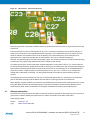
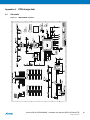
1
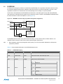
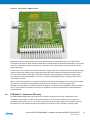
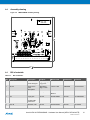
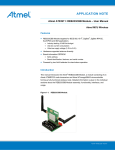
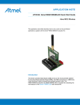
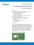
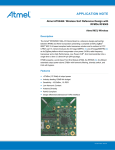
APPLICATION NOTE
Atmel AVR2162: REB233SMAD – Hardware User Manual
8-bit Atmel Microcontrollers
Features
•
High-performance 2.4GHz RF-CMOS Atmel® AT86RF233 radio transceiver
targeted for IEEE® 802.15.4, ZigBee®, ZigBee RF4CE, 6LoWPAN and ISM
applications
• Industry leading 101dB linkbudget
• Ulta-low current consumption
• Ultra-low supply voltage (1.8V to 3.6V)
•
•
•
•
Hardware supported antenna diversity
RF reference design and high-performance evaluation platform
Interfaces to several of the Atmel microcontroller development platforms
Board information EEPROM
• MAC address
• Board identification, features, and serial number
• Crystal calibration values
Introduction
This manual describes the REB233SMAD radio extender board supporting antenna
diversity in combination with the Atmel AT86RF233 radio transceiver. Detailed
information is given in the individual sections about the board functionality, the board
interfaces, and the board design.
The REB233SMAD connects directly to the REB controller base board (REB-CBB),
or can be used as an RF interface in combination with one of the Atmel
microcontroller development platforms. The REB233SMAD together with a
microcontroller forms a fully functional wireless node.
Figure 1.
REB233SMAD Radio Extender Board.
42006B−AVR−07/2012
Table of Contents
1. Disclaimer ............................................................................................ 3 2. Overview .............................................................................................. 3 3. Functional description .......................................................................... 3 3.1 Interface connector specification ....................................................................... 4 3.1.1 Atmel ATmega1281 configuration ....................................................... 4 3.1.2 Atmel ATmega644 configuration ......................................................... 5 3.2 ID EEPROM ...................................................................................................... 6 3.3 Supply current sensing...................................................................................... 7 3.4 Radio transceiver reference clock ..................................................................... 8 3.5 RF section ......................................................................................................... 8 4. PCB layout description ......................................................................... 9 4.1 PCB detail 1 – balanced RF pin fan out .......................................................... 10 4.2 PCB detail 2 – RF switch ................................................................................ 11 4.3 PCB detail 3 – crystal routing .......................................................................... 11 4.4 PCB detail 4 – transceiver analog GND routing .............................................. 12 4.5 PCB detail 5 – digital GND routing and shielding ............................................ 13 4.6 PCB detail 6 – transceiver RF tuning .............................................................. 14 4.7 Antenna connection ........................................................................................ 15 5. Mechanical description ...................................................................... 16 6. Electrical characteristics .................................................................... 17 6.1 Absolute maximum ratings .............................................................................. 17 6.2 Recommended operating range ...................................................................... 18 6.3 Current consumption ....................................................................................... 18 6.4 Duty cycle requirements .................................................................................. 19 7. Abbreviations ..................................................................................... 19 Appendix A. PCB design data ........................................................... 20 A.1 Schematic ....................................................................................................... 20 A.2 Assembly drawing ........................................................................................... 21 A.3 Bill of materials ................................................................................................ 21 Appendix B. Radio certification .......................................................... 23 B.1 United States (FCC) ........................................................................................ 23 B.2 Europe (ETSI) ................................................................................................. 24 B.3 Approved antenna ........................................................................................... 24 8. References ......................................................................................... 25 9. Revision history REB233SMAD PCBA .............................................. 26 10. EVALUATION BOARD/KIT IMPORTANT NOTICE ........................... 27 Atmel AVR2162: REB233SMAD – Hardware User Manual [APPLICATION NOTE]
42006B−AVR−07/2012
2
1.
Disclaimer
Typical values contained in this application note are based on simulations and testing of individual examples.
Any information about third-party materials or parts was included in this document for convenience. The vendor may
have changed the information that has been published. Check the individual vendor information for the latest changes.
2.
Overview
The radio extender board is assembled with an Atmel AT86RF233 radio transceiver [1] and equipped with two SMA
connectors to support antenna diversity. External antennas can be connected to the SMA ports as well as RF
measurement equipment for performance evaluation of the radio transceiver. The radio transceiver is able to switch
between these two antenna ports to select the best receiving path in harsh multipath environments.
The radio extender board was designed to interface to the Atmel microcontroller development or evaluation platforms
(for example, Atmel STK®500). The microcontroller platform in combination with the REB provides an ideal way to:
•
Evaluate the outstanding radio transceiver performance, such as the excellent receiver sensitivity achieved at
ultra-low current consumption
•
•
Test the radio transceiver’s comprehensive hardware support of the IEEE 802.15.4™-2011 standard
Test the radio transceiver’s enhanced feature set, which includes antenna diversity, AES, high data rate
modes and reduce power consumption modes
Figure 2-1 shows a development and evaluation setup using the REB controller base board (REB-CBB) [2] in
combination with the REB233SMAD radio extender board; via SMA connectors which are assembled with quarter wave
rotate and tilt antennas.
Figure 2-1. The REB233SMAD connected to a REB-CBB.
3.
Functional description
The block diagram of the REB233SMAD radio extender board is shown in Figure 3-1. The power supply pins and all
digital I/Os of the radio transceiver are routed to the 2 × 20-pin expansion connector to interface to a power supply and
a microcontroller.
Atmel AVR2162: REB233SMAD – Hardware User Manual [APPLICATION NOTE]
42006B−AVR−07/2012
3
The Atmel AT86RF233 antenna diversity (AD) feature supports the control of two antennas which can be assembled on
top of the SMA connectors. A digital control pin (DIG1) is used to control an external RF switch selecting one of the two
antennas. During the RX listening period, the radio transceiver continuously switches in between the two antennas
autonomously, without the need for microcontroller interaction, if the AD feature is enabled [1]. Once an IEEE 802.15.4
synchronization header is detected, the antenna providing sufficient signal quality is selected to receive the remaining
frame. This ensures reliability and robustness, especially in harsh environments with strong multipath fading effects [4].
Board-specific information such as board identifier, the node MAC address, and production calibration values are stored
in an ID EEPROM. The SPI bus of the EEPROM is shared with the radio transceiver’s interface.
Figure 3-1. REB233SMAD block diagram.
JP1
DEVDD
Protection
GND
TP7
TP6
DIG3
DIG4
X2
Balun
RFSwitch
RSTN
DIG2
RFP
AT86RF233
IRQ
SLPTR
RFN
CLKM
X3
ID
EEPROM
XTAL
EXPAND1
DIG2
SPI
XTAL2
XTAL1
DIG1
4
REB233SMAD
3.1
Interface connector specification
The REB is equipped with a 2 × 20-pin, 100mil, expansion connector, X1. The pin assignment enables a direct interface
to the REB-CBB [2]. Further, the interface connects to the Atmel STK500/501 microcontroller development platform to
enable support for various Atmel 8-bit AVR® microcontrollers.
The REB (2 × 20-pin X1 connector) is preconfigured to interface to an STK501 with an Atmel ATmega1281 or a
Controller Base Board with an Atmel ATxmega 256A3 respectively.
To operate the REB with an Atmel ATmega644 on STK500, the 0Ω resistors R10 through R18 must be removed and
re-installed on the board manually as resistors R20 through R28 (see Appendix A).
Other microcontroller development platforms need to be interfaced using a special adapter board.
3.1.1
Atmel ATmega1281 configuration
Table 3-1.
Default expansion connector mapping (ATmega1281 configuration).
Pin#
Function
Pin#
Function
1
GND
2
GND
3
n.c.
4
n.c.
5
n.c.
6
n.c.
7
n.c.
8
n.c.
9
n.c.
10
n.c.
11
n.c.
12
n.c.
Atmel AVR2162: REB233SMAD – Hardware User Manual [APPLICATION NOTE]
42006B−AVR−07/2012
4
Pin#
Function
Pin#
Function
13
n.c.
14
n.c.
15
n.c.
16
n.c.
18
n.c.
17
n.c., optionally XT1 (MCLK)
19
VCC
20
VCC
21
GND
22
GND
23
PB7 (open)
24
PB6 (open)
25
PB5 (RSTN)
26
PB4 (SLPTR)
27
PB3 (MISO)
28
PB2 (MOSI)
29
PB1 (SCLK)
30
PB0 (SEL)
31
PD7 (TP1)
32
PD6 (MCLK)
33
PD5 (TP2)
34
PD4 (DIG2)
35
PD3 (TP3)
36
PD2 (open)
37
PD1 (TP4)
38
PD0 (IRQ)
39
GND
40
EE#WP (write protect EEPROM)
Note:
3.1.2
(1)
1.
Possible by retrofitting a 0R assembly.
Atmel ATmega644 configuration
Table 3-2.
Expansion connector mapping when assembled for ATmega644.
Pin#
Function
Pin#
Function
1
GND
2
GND
3
n.c.
4
n.c.
5
n.c.
6
n.c.
7
n.c.
8
n.c.
9
n.c.
10
n.c.
11
n.c.
12
n.c.
13
n.c.
14
n.c.
15
n.c.
16
n.c.
18
n.c.
(1)
17
n.c., optionally XT1 (MCLK)
19
VCC
20
VCC
21
GND
22
GND
23
PB7 (SCLK)
24
PB6 (MISO)
25
PB5 (MOSI)
26
PB4 (SEL)
27
PB3 (open)
28
PB2 (RSTN)
29
PB1 (MCLK)
30
PB0 (open)
31
PD7 (SLPTR)
32
PD6 (DIG2)
33
PD5 (TP2)
34
PD4 (open)
35
PD3 (TP3)
36
PD2 (IRQ)
37
PD1 (TP4)
38
PD0 (open)
39
GND
40
EE#WP (write protect EEPROM)
Note:
1.
Possible by retrofitting a 0R assembly.
Atmel AVR2162: REB233SMAD – Hardware User Manual [APPLICATION NOTE]
42006B−AVR−07/2012
5
3.2
ID EEPROM
To identify the board type by software, an identification (ID) EEPROM, U5, is populated. Information about the board,
the node MAC address and production calibration values are stored here. An Atmel AT25010B [3] with 128 × 8-bit
organization and SPI bus is used because of its small package and low-voltage / low-power operation.
The SPI bus is shared between the EEPROM and the transceiver. The select signal for each SPI slave (EEPROM,
radio transceiver) is decoded with the reset line of the transceiver, RSTN. Therefore, the EEPROM is addressed when
the radio transceiver is held in reset (RSTN = 0; see Figure 3-2).
Figure 3-2. EEPROM access decoding logic (Atmel ATmega1281 configuration).
PB5 (RSTN)
RSTN
PB0 (SEL)
>1
SEL#
/RST
/SEL
Transceiver
AT86RF233
SPI
PB1..3 (SPI)
>1
#CS
On-Board
EEPROM
The EEPROM data are written during board production testing. A unique serial number, the MAC address , and
calibration values are stored. These can be used to optimize system performance.
Note:
1.
MAC addresses used for this package are Atmel property. The use of these MAC addresses for development
purposes is permitted.
Table 3-3 shows a detailed description of the EEPROM data structure.
Table 3-3.
ID EEPROM mapping.
Address
Name
Type
Description
0x00
MAC address
uint64
MAC address for the 802.15.4 node, little endian byte order
0x08
Serial number
uint64
Board serial number, little endian byte order
0x10
Board family
uint8
Internal board family identifier
0x11
Revision
uint8[3]
Board revision number ##.##.##
Board features, coded into seven bits
0x14
Feature
uint8
7
Reserved
6
Reserved
5
External LNA
4
External PA
3
Reserved
2
Diversity
1
Antenna
0
SMA connector
Atmel AVR2162: REB233SMAD – Hardware User Manual [APPLICATION NOTE]
42006B−AVR−07/2012
6
Address
Name
Type
Description
0x15
Cal OSC 16MHz
uint8
RF233 XTAL calibration value, register XTAL_TRIM
0x16
Cal RC 3.6V
uint8
Atmel ATmega1281 internal RC oscillator calibration value @
3.6V, register OSCCAL
0x17
Cal RC 2.0V
uInt8
Atmel ATmega1281 internal RC oscillator calibration value @
2.0V, register OSCCAL
0x18
Antenna gain
Int8
Antenna gain [resolution 1/10dBi].
For example, 15 will indicate a gain of 1.5dBi.
The values 00h and FFh are per definition invalid. Zero or
-0.1dBi has to be indicated as 01h or FEh
0x20
Board name
Char[30]
Textual board description
0x3E
CRC
Uint16
16-bit CRC checksum, standard ITU-T generator polynomial
G16(x) = x16 + x12 + x5 + 1
Figure 3-3. Example EEPROM dump.
-----| EEPROM dump |-------------0000 - 8F 5C 17 FF FF 25 04 00 70 02 00 00 40 00 00 00
.\...%..p...@...
0010 - 00 08 01 00 05 04 A9 AA 00 FF FF FF FF FF FF FF
................
0020 - 52 45 42 32 33 33 53 4D 41 44 00 00 00 00 00 00
REB233SMAD......
0030 - 00 00 00 00 00 00 00 00 00 00 00 00 00 00 F5 06
................
0040 - FF FF FF FF FF FF FF FF FF FF FF FF FF FF FF FF
................
0050 - FF FF FF FF FF FF FF FF FF FF FF FF FF FF FF FF
................
0060 - FF FF FF FF FF FF FF FF FF FF FF FF FF FF FF FF
................
0070 - FF FF FF FF FF FF FF FF FF FF FF FF FF FF FF FF
................
----------------------------------
3.3
Supply current sensing
A jumper, JP1, is placed in the supply voltage trace to offer an easy way for current sensing. The current consumption
of all circuitry connected to the supply domains DEVDD/EVDD such as AT86RF233 and AT25010B can be measured
by connecting an ampere meter instead of the jumper bridge JP1, see Figure 3-4 on page 8
The power supply pins of the radio transceiver are protected against overvoltage stress and reverse polarity at the X1
connector pins (net CVTG, net DGND) using a Zener diode, D1, and a thermal fuse, F1, (see Appendix A). This is
required because the Atmel STK500 will provide 5V as default voltage, and the board can also be mounted with reverse
polarity.
Depending on the actual supply voltage, the diode D1 can consume several milliamperes. This has to be considered
when the current consumption of the whole system is measured. In such a case, D1 should be removed from the board.
To achieve the best RF performance, the analog (EVDD) and digital (DEVDD) supply are separated from each other by
a CLC PI-filter. Digital and analog ground planes are connected together on the bottom layer, underneath the radio
transceiver IC. Further details are described in Section 4, page 9.
Note:
All components connected to nets DEVDD/EVDD contribute to the total current consumption.
While in radio transceiver SLEEP state, most of the supply current is drawn by the 1MΩ pull-up resistor, R24, connected
to the ID EEPROM and the EEPROM standby current.
Atmel AVR2162: REB233SMAD – Hardware User Manual [APPLICATION NOTE]
42006B−AVR−07/2012
7
Figure 3-4. Power supply routing.
3.4
Radio transceiver reference clock
The integrated radio transceiver is clocked by a 16MHz reference crystal, Q1. The 2.4GHz modulated signal is derived
from this clock. Operating the node according to IEEE 802.15.4 [5], the reference frequency must not exceed a
deviation of ±40ppm. The absolute frequency is mainly determined by the external load capacitance of the crystal,
which depends on the crystal type and is given in its datasheet.
The radio transceiver reference crystal, Q1, shall be isolated from fast switching digital signals and surrounded by a
grounded guard trace to minimize disturbances of the oscillation. Detailed layout considerations can be found in
Section 4.3, page 11.
The REB uses a Siward SX4025 crystal with two load capacitors of 10pF each. To compensate for fabrication and
environment variations, the frequency can be further tuned using the radio transceiver register XOSC_CTRL (0x12)
(refer to [1], Section References). The REB production test guarantees a tolerance of within +20ppm and -5ppm. The
correction value, to be applied to TRX register XOSC_CTRL (0x12), is stored in the onboard EEPROM (see
Section 3.2, page 6).
The reference frequency is also available at pin CLKM of the radio transceiver and, depending on the related register
setting; it is divided by an internal prescaler. CLKM clock frequencies of 16MHz, 8MHz, 4MHz, 2MHz, 1MHz, 250kHz,
or 62.5kHz are programmable (refer to [1]). The CLKM signal is filtered by a low-pass filter to reduce harmonic
emissions within the 2.4GHz ISM band. The filter is designed to provide a stable 1MHz clock signal with correct logic
level to a microcontroller pin with sufficiently suppressed harmonics. CLKM frequencies above 1MHz require a redesign
of R25 and C40. In case of RC cut-off frequency adjustments, depending on the specific load and signal routing
conditions, one may observe performance degradation of channel 26.
Note:
Channel 26 (2480MHz) is affected by the following harmonics: 155 × 16MHz or 310 × 8MHz.
By default, CLKM is routed to a microcontroller timer input; check the individual configuration resistors in the schematic
drawing. To connect CLKM to the microcontroller main clock input, assemble R3 with a 0Ω resistor.
3.5
RF section
The Atmel AT86RF233 radio transceiver incorporates all RF and base band critical components, necessary to transmit
and receive signals according to IEEE 802.15.4 or proprietary ISM data rates.
The balun, B1, performs the differential to single-ended conversion of the RF signal to connect the AT86RF233 to the
RF switch, U1. The RF switch is controlled by the radio transceiver output, DIG1, and selects one of the two antennas.
The output signal is routed to the edge mounted SMA connectors, X2 and X3. The /4 antennas, provided with the
board can rotate and tilt. Detailed information about the antenna diversity feature are given in [1] and [4].
Atmel AVR2162: REB233SMAD – Hardware User Manual [APPLICATION NOTE]
42006B−AVR−07/2012
8
To estimate the effective output power for the SMA connector reference plane, the balun, the switch and transmission
line losses have to be taken into account. Therefore, in worst case, the SMA connector output power can be up to
1.5dB below the datasheet value, specified for the AT86RF233. Insertion loss data for the individual components can be
obtained from associated datasheets. Please check the part reference inside the BOM in section A.3.
4.
PCB layout description
This section describes critical layout details to be carefully considered during a PCB design. The PCB design requires
an optimal solution for the following topics:
•
Create a solid ground plane as a stable reference for the transceiver, the antenna and the transmission lines.
The PCB has to be considered as a part of the antenna; it interacts with the radiated electromagnetic wave
•
•
Isolate digital noise from the antenna and the radio transceiver to achieve optimum range and RF performance
•
Reduce any kind of spurious emissions below the limits set by the individual regulatory organizations
Isolate digital noise from the 16MHz reference crystal to achieve optimum transmitter and receiver
performance
The REB233SMAD PCB design further demonstrates a low-cost, two-layer PCB solution without the need of an inner
ground plane.
The drawing in Figure 4-1 shows critical sections using numbered captions. Each caption number has its own
subsection below with detailed information.
Figure 4-1. Board layout sections with detail descriptions.
Atmel AVR2162: REB233SMAD – Hardware User Manual [APPLICATION NOTE]
42006B−AVR−07/2012
9
4.1
PCB detail 1 – balanced RF pin fan out
Figure 4-2. Board layout – RF pin fan out.
The Atmel AT86RF233 antenna port should be connected to a 100Ω load with a small series inductance of 1nH to 2nH.
This is achieved with the connection fan out in between the IC pins and the filter balun combination B1. The trace width
is kept small at 0.2mm for a length of approximately 1.5mm. The REB233SMAD is a two-layer FR4 board with a
thickness of 1.5mm. Therefore, the distributed capacitance between top and bottom is low, and transmission lines are
rather inductive.
B1 has the DC blocking built in. Only pin 2 requires DC blocking within its GND connection since this is considered as
bias access pin.
The distance of 1.5mm in between B1 and U3 also allows GND vias for pin 3 and pin 6 of the AT86RF233. The GND
connection in a low distance has a small parasitic inductance and is therefore desirable for the RF port.
Atmel AVR2162: REB233SMAD – Hardware User Manual [APPLICATION NOTE]
42006B−AVR−07/2012
10
4.2
PCB detail 2 – RF switch
Figure 4-3. Board layout – RF switch.
The RF switch requires a solid grounding to achieve the full isolation and RF filter capacitors for the control pins.
A parasitic inductance within the ground connection may reduce the RF isolation of the switch output in the off state. To
achieve a hard, low-impedance ground connection, several vias are placed on each side of the ground pad. The ground
pad is connected to the top layer ground plane in addition.
Blocking capacitors C24 and C25 are placed as close as possible to the RF switch to short any control line noise. Noise
interfering on the control pins may cause undesired modulation of the RF signal. Therefore these parts are marked as
noise shunt.
C11 and C12 will block any DC voltage on the RF line. On the input side, C28, next to the balun provides the required
DC blocking.
4.3
PCB detail 3 – crystal routing
The reference crystal PCB area requires optimization to minimize external interference and to keep any radiation of
16MHz harmonics low.
Since the board design incorporates a shield, the crystal housing has been tied hard to ground. This method will
minimize the influence of external impairments such as burst and surge.
To prevent crosstalk, the crystal is encircled by a ring of ground traces and vias. Special care has to be taken in the
area between the IRQ line and the crystal. Depending on the configuration, the interrupt may be activated during a
frame receive. Crosstalk into the crystal lines would increase the phase noise and therefore reduce the signal to noise
ratio.
Atmel AVR2162: REB233SMAD – Hardware User Manual [APPLICATION NOTE]
42006B−AVR−07/2012
11
Figure 4-4. Board layout – XTAL section.
The reference crystal and its load capacitors C37/38 form the resonator circuit. These capacitors are to be placed close
to the crystal. The ground connection in between the capacitors should be a solid copper area right underneath the
crystal, including the housing contacts.
4.4
PCB detail 4 – transceiver analog GND routing
With the Atmel AT86RF233, consider pins 3, 6, 27, 30, 31, and 32 as analog ground pins. Pin 7 is an exception and can
be connected to the central paddle like the other analog ground pins.
Analog ground pins are to be routed to the paddle underneath the IC. The trace width has to be similar to the pad width
when connecting the pads, and increase, if possible, in some distance from the pad. This measure will decrease the
parasitic inductance as far as possible.
Each ground pin should be connected to the bottom plane with at least one via. Move the vias as close to the IC as
possible. It is always desired to integrate the single-pin ground connections into polygon structures after a short
distance. Top, bottom, and, on multilayer boards, the inner ground planes, should be tied together with a grid of vias.
When ground loops are smaller than one tenth of the wavelength, it is safe to consider this as a solid piece of metal.
Atmel AVR2162: REB233SMAD – Hardware User Manual [APPLICATION NOTE]
42006B−AVR−07/2012
12
Figure 4-5. Board layout – transceiver GND.
The soldering technology used allows the placement of small vias (0.15mm drill) within the ground paddle underneath
the chip. During reflow soldering, the vias get filled with solder, having a positive effect on the connection cross section.
The small drill size keeps solder losses within an acceptable limit. During the soldering process vias should be open on
the bottom side to allow enclosed air to expand.
4.5
PCB detail 5 – digital GND routing and shielding
With the Atmel AT86RF233, consider pins 12, 16, 18, and 21 as digital ground pins.
Digital ground pins are not directly connected to the center paddle. Digital ground pins may carry digital noise from I/O
pad cells or other digital processing units within the chip.
In case of a direct paddle connection, impedances of the paddle ground vias could cause a small voltage drop for this
noise and may result in an increased noise level transferred to the analog domain.
There is a number of pro’s and con’s when it comes to the shielding topic. The major con’s are:
•
•
•
Cost of the shield
Manufacturing effort
Inaccessibility for test and repair
The number of pro’s might be longer but the cost argument is often very strong. However, the reasons to add the shield
for this reference design are:
•
•
•
Shield is required for a certification in Japan
Shield is recommended for FCC certification in North America
Increased performance
Atmel AVR2162: REB233SMAD – Hardware User Manual [APPLICATION NOTE]
42006B−AVR−07/2012
13
Figure 4-6. Board layout – GND and shield.
Besides the function to provide supply ground to the individual parts, the ground plane has to be considered as a
counterpart for the antenna. Such an antenna base plate is required to achieve full antenna performance. It has to be a
continuous, sustained metal plate for that purpose. The shield, covering the electronic section will help to form this
antenna base plate.
For that reason, any unused surface should be filled with a copper plane and connected to the other ground side using
sufficient through hole contacts. Larger copper areas should also be connected to the other side layer with a grid of
vias. This will form kind of a RF sealing for the FR4 material. Any wave propagation in between the copper layers
across the RF4 will become impossible. This way, for an external electromagnetic field, the board will behave like a
coherent piece of metal.
When a trace is cutting the plane on one side, the design should contain vias along this trace to bridge the interrupted
ground on the other side. Place vias especially close to corners and necks to connect lose polygon ends.
The pads where the shield is mounted also need some attention. The shield has to be integrated in the ground planes.
Vias, in a short distance to the pads, will ensure a low impedance connection and also close the FR4 substrate as
mentioned above.
4.6
PCB detail 6 – transceiver RF tuning
The REB233SMAD implements a tuning structure to optimize the transceiver matching. A transmission line in
combination with a capacitor is used to vary the load impedance. Under normal conditions only one capacitor is
assembled at position C23, C26, or C27. These three positions allow varying the position of the capacitor along the
transmission line. The capacitance value and the position of the capacitor can be changed to tune the system.
Atmel AVR2162: REB233SMAD – Hardware User Manual [APPLICATION NOTE]
42006B−AVR−07/2012
14
Figure 4-7. Board layout – transceiver RF tuning.
During tuning the best compromise in between RX and TX performance has to be found. Tuning should be done for the
receiver first.
First step should be to verify the 50Ω matching at U1, pin 5. To measure this impedance with a network analyzer, U1
needs to be removed and a 1mm rigid cable should be connected to pin 5. Measurements from X2 and X3 are much
harder to calibrate. The transceiver has to be set to state RX_ON for that measurement. If the transceiver is not
powered and is in a state other than RX_ON, the measured S11 will not show reasonable impedance.
After that, the capacitor position and value can be slightly varied. The reception performance should be measured using
a packet error test. Typical tuning capacitor values are in between 0.5pF and 1pF.
To simplify the tuning, the receiver input power should be adjusted to a value where a PER of ~1% can be measured.
For the measurement 5.000 to 10.000 frames should be used to get a clear PER value. After a board tuning change the
PER should be measured with the same environment as before. Now the new sensitivity can be evaluated based on a
simple rule of thumb. A PER change by one decimal power (from 1% up to 10%, or down to 0.1%) corresponds in
average with a 1dB change in sensitivity. The tuning measurements have to take the whole frequency band into
account.
The matching point for best sensitivity can, but may not be identical with the best S11 matching point. The matching
point for the lowest noise figure will be different from the best S11 matching point that can be measured.
When satisfying reception sensitivity was achieved, the transmitter performance should be tested as well for the current
tuning step. Main parameters are transmitting power, EVM, spurious emissions and performance flatness over the
whole frequency band. Goal is to maximize the link budged, calculated from sensitivity and transmits power.
4.7
Antenna connection
The board was constructed with the two SMA connectors at the left and right side to allow antennas to be connected. A
good choice in between flexibility and performance is a quarter wave antenna with rotate and tilt option.
Antenna origin details:
Vendor:
Tekfun Co., Ltd.
Type:
M35-S, Swivel SMA male
Atmel AVR2162: REB233SMAD – Hardware User Manual [APPLICATION NOTE]
42006B−AVR−07/2012
15
Figure 4-8. Antenna tuning structure.
The board design implements additional footprints for a pi-network to tune short antennas correctly against the board
ground plane. For the antenna delivered with the board, this is not required and therefore C13, C14, C15, and C16 are
unassembled.
5.
Mechanical description
The REB233SMAD is manufactured using a low-cost, two-layer printed circuit board. All components and connectors
are mounted on the top side of the board.
The format was defined to fit the EXPAND1 connector on the Atmel AVR STK500/STK501 microcontroller evaluation
board. The upright position was chosen for best antenna performance.
Atmel AVR2162: REB233SMAD – Hardware User Manual [APPLICATION NOTE]
42006B−AVR−07/2012
16
Figure 5-1. Mechanical outline (dimensions in mm).
Table 5-1.
RED233SMAD mechanical dimensions.
Dimension
Value
Width x
57mm
Width y
61mm
6.
Electrical characteristics
6.1
Absolute maximum ratings
Stresses beyond the values listed in Table 6-1 may cause permanent damage to the board. This is a stress rating only
and functional operation of the device at these or any other conditions beyond those indicated in the operational
sections of this manual are not implied. Exposure to absolute maximum rating conditions for extended periods may
affect device reliability. For more details about these parameters, refer to individual datasheets of the components used.
Atmel AVR2162: REB233SMAD – Hardware User Manual [APPLICATION NOTE]
42006B−AVR−07/2012
17
Table 6-1.
Absolute maximum ratings.
No.
Parameter
7.1.1
Storage temperature range
7.1.2
Humidity
7.1.3
Supply voltage
-0.3
+3.6
V
7.1.4
EXT I/O pin voltage
-0.3
VCC + 0.3
V
7.1.5
Supply current from batteries
+70
A
7.1.6
Condition
-40
Sum over all power pins
(1)
Maximum
1.
6.2
Recommended operating range
Unit
+85
°C
90
% r.H.
0
Note:
mA
Keep power switch off or remove battery from REB-CBB when external power is supplied.
Recommended operating range.
No.
Parameter
Condition
7.2.1
Operating temperature range
Crystal within ±40ppm
7.2.2
Supply voltage (VCC)
6.3
Typical
Non-condensing
Battery Charge current
Table 6-2.
Minimum
Minimum
Typical
-20
1.8
3.0
Maximum
Unit
+70
°C
3.6
V
Current consumption
Test conditions (unless otherwise stated):
VDD = 3.0V, TOP = 25°C
Table 6-3 lists current consumption values for typical scenarios of a complete system composed of REB-CBB and
REB233. The Zener diode D1 has been removed as described above.
Table 6-3.
Current consumption of REB-CBB populated with REB233.
No.
Parameter
Condition
Minimum
Typical
7.3.1
Supply current
MCU @ power down,
transceiver in state SLEEP,
serial flash in Deep-Sleep
17 (1)
Supply current
MCU @ 2MHz,
transceiver in state TRX_OFF
3 (1)
7.3.3
Supply current
MCU @ 16MHz (int. RC 32MHz),
transceiver in state TRX_OFF
15 (1)
7.3.4
Supply current
MCU @ 16MHz (int. RC 32MHz),
transceiver in state RX_ON
28 (1)
7.3.5
Supply current
MCU @ 16MHz (int. RC 32MHz),
transceiver in state BUSY_TX
26 (1)
1.
Unit
µA
7.3.2
Note:
Maximum
mA
mA
mA
mA
Measurement results with D1 removed.
Atmel AVR2162: REB233SMAD – Hardware User Manual [APPLICATION NOTE]
42006B−AVR−07/2012
18
6.4
Duty cycle requirements
Table 6-4.
TX operating condition.
No.
Parameter
Condition
7.4.1
TX Duty Cycle OQPSK(1)
over 100ms
IEEE802.15.4 channel 26
Note:
1.
Minimum
Typical
Maximum
31
Unit
%
To ensure FCC compliant operation for the OQPSK operating mode in IEEE802.51.4 channel 26, the TX duty cycle
has to be equal or below the specified maximum value under normal and extreme conditions. The duty cycle for
other channels is not restricted. For DCSS operation the maximum limit is 3% at frequency 2.481GHz.
For further details refer to VNR-E33SD-X5B-00 FCC test report.
7.
Abbreviations
802.15.4
-
IEEE 802.15.4-standard, applicable to low-rate wireless Personal Area Network
AD
-
Antenna diversity
AES
-
Advanced encryption standard
BB
-
Baseband
CBB/REB-CBB -
Controller base board
CRC
-
Cyclic redundancy check
ETSI
-
European Telecommunications Standards Institute
EVM
-
Error Vector Magnitude
FCC
-
Federal Communications Commission
ISM
-
Industrial, scientific and medical (frequency band)
LNA
-
Low-noise amplifier
MAC
-
Medium access control
NWA
-
Network analyzer
PA
-
Power amplifier
PER
-
Packet error rate
R&TTE
-
Radio and Telecommunications Terminal Equipment
(Directive of the European Union)
REB
-
Radio extender board
RF
-
Radio frequency
RX
-
Receiver
S11
-
Input port voltage reflection coefficient, one of the scattering (S-)parameters, describes the input
matching to the reference system (50 or 75 Ohms)
SMA
-
Sub-miniature-A (connection)
SPI
-
Serial peripheral interface
TX
-
Transmitter
XTAL
-
Crystal
Atmel AVR2162: REB233SMAD – Hardware User Manual [APPLICATION NOTE]
42006B−AVR−07/2012
19
Appendix A.
A.1
PCB design data
Schematic
Figure 7-1. REB233SMAD schematic.
Atmel AVR2162: REB233SMAD – Hardware User Manual [APPLICATION NOTE]
42006B−AVR−07/2012
20
A.2
Assembly drawing
Figure 7-2. REB233SMAD assembly drawing.
A.3
Bill of materials
Table 7-1.
Bill of materials.
Qty.
Designator
Description
Footprint
Manuf. Part#
Manufacturer
Comment
1
X1
Pin header
2×20 90 degree
JP_2×20_90°_
Top_Invers
1007-121-40
CAB
HEADER-20X2
2
X2, X3
End Launch
Jack
Receptacle
SMA Board
Edge, 1.6mm
142-0711-821
EMERSON
Round Contact
1
U5
EEPROM
MiniMap-8-2X3
AT25010BMAHL-T
Atmel
AT25010B
1
U4
Logic gate
SC70-8
NV7WP32K8X
Fairchild
NC7WP32K8X
1
U3
802.15.4
2.4GHz radio
transceiver
MLF-32
AT86RF233
Atmel
AT86RF233
2
U2, U6
Dual INV, ULP
SC70-6
NC7WV04P6X
Fairchild
NC7WV04
1
U1
RF switch
SC70-6
AS222-92
SkyWorks
AS222-92
Atmel AVR2162: REB233SMAD – Hardware User Manual [APPLICATION NOTE]
42006B−AVR−07/2012
21
Qty.
Designator
Description
Footprint
Manuf. Part#
Manufacturer
Comment
1
SH1
SMT RF Shield
Shield-BMIS
LT08AD4303F
Laird
Frame&Lid
9
R5, R7, R10, R12, R14,
R17, R19, R21, R23
Resistor
0603H0.5
Samsung
0Ω
2
R29, R30
Resistor
0402A
Samsung
0Ω
1
R32
Resistor
0402A
Samsung
22Ω
1
R25
Resistor
0402A
Samsung
470Ω
2
R8, R15
Resistor
0402A
Samsung
2.2kΩ
2
R27, R28
Resistor
0402A
Samsung
10kΩ
2
R24, R26
Resistor
0402A
Samsung
1MΩ
1
Q1
Crystal 16MHz
XTAL_4X2_5_
Small
XTL551150NLE16.0MHz-9.0R
Siward
SX-4025 16MHz
1
L1
SMT ferrite
bead
0603H0.8
74279263
Würth
220Ω@100MHz
1
JP1
Jumper 2-pole
JP_2x1
1001-121-002
CAB
JP-2
1
J3
Jumper cap
3300096
CAB
1
F1
PTC fuse
1812
miniSMDC020
Raychem
miniSMDC020
1
D1
Z-Diode
DO-214AC
BZG05C3V9
Vishay
BZG05C3V9
2
C37, C38
Capacitor
0402A
Panasonic
10pF/5%
2
C35, C36
Capacitor
0402A
Kemet
1µF
6
C30, C31, C32, C33, C34,
C39
Capacitor
0402A
Murata
100n
6
C11, C12, C24, C25, C28,
C29
Capacitor
0402A
Kyovera-elco
22pF
1
C40
Capacitor
0402A
Murata
2.2pF
1
C23
Capacitor
0402A
Generic G0G
1.2pF
1
B1
Balun
0805-6
JTI
Johanson
2.4GHz Filtered
Balun
2450FB15L0001E
Atmel AVR2162: REB233SMAD – Hardware User Manual [APPLICATION NOTE]
42006B−AVR−07/2012
22
Appendix B.
Radio certification
The wireless radio node consisting of:
1.
2.
3.
4.
Radio Extender Board REB233SMAD (as described in this application note), assembled with
Two 2.4GHz Omni Rubber Antennas M35-S [9], mounted on a
REB Controller Base Board (REB-CBB [2]), which hosts an application firmware available with
Atmel AVR2025: IEEE 802.15.4 MAC Software Package [10]
has received regulatory approvals for modular devices in the United States and European countries. The wireless node
is shown in Figure 2-1.
B.1
United States (FCC)
Compliance Statement (Part 15.19)
The device complies with Part 15 of the FCC rules. To fulfill FCC Certification requirements, an Original Equipment
Manufacturer (OEM) must comply with the following regulations:
•
The modular transmitter must be labeled with its own FCC ID number, and, if the FCC ID is not visible when
the module is installed inside another device, the outside of the device into which the module is installed must
also display a label referring to the enclosed module
•
This exterior label can use wording such as the following. Any similar wording that expresses the same
meaning may be used
Contains FCC-ID: VNR-E33SD-X5B-00
This device complies with Part 15 of the FCC Rules. Operation is subject to the following
two conditions: (1) this device may not cause harmful interference, and (2) this device must
accept any interference received, including interference that may cause undesired
operation.
Use in portable exposure conditions (FCC 2.1093) requires separate equipment authorization. Modifications not
expressly approved by this company could void the user's authority to operate this equipment (FCC Section 15.21).
Compliance Statement (Part 15.105(b))
This equipment has been tested and found to comply with the limits for a Class B digital device, pursuant to Part 15 of
the FCC Rules. These limits are designed to provide reasonable protection against harmful interference in a residential
installation. This equipment generates uses and can radiate radio frequency energy and, if not installed and used in
accordance with the instructions, may cause harmful interference to radio communications. However, there is no
guarantee that interference will not occur in a particular installation. If this equipment does cause harmful interference to
radio or television reception, which can be determined by turning the equipment off and on, the user is encouraged to
try to correct the interference by one or more of the following measures:
•
•
•
•
Reorient or relocate the receiving antenna
Increase the separation between the equipment and receiver
Connect the equipment into an outlet on a circuit different from that to which the receiver is connected
Consult the dealer or an experienced radio/TV technician for help
Atmel AVR2162: REB233SMAD – Hardware User Manual [APPLICATION NOTE]
42006B−AVR−07/2012
23
IMPORTANT FCC NOTICE to USERS
Warning:
Changes or modifications not expressly approved by this company could void the user’s authority to operate the
equipment.
B.2
Europe (ETSI)
If the device is incorporated into a product, the manufacturer must ensure compliance of the final product to the
European harmonized EMC and low-voltage/safety standards. A Declaration of Conformity must be issued for each of
these standards and kept on file as described in Annex II of the R&TTE Directive.
The manufacturer must maintain a copy of the device documentation and ensure the final product does not exceed the
specified power ratings, and/or installation requirements as specified in the user manual. If any of these specifications
are exceeded in the final product, a submission must be made to a notified body for compliance testing to all required
standards. The “CE“ marking must be affixed to a visible location on the OEM product. The CE mark shall consist of the
initials "CE" taking the following form:
•
If the CE marking is reduced or enlarged, the proportions given in the above graduated drawing must be
respected
•
The CE marking must have a height of at least 5mm except where this is not possible on account of the nature
of the apparatus
•
The CE marking must be affixed visibly, legibly, and indelibly
More detailed information about CE marking requirements you can find at "DIRECTIVE 1999/5/EC OF THE
EUROPEAN PARLIAMENT AND OF THE COUNCIL" on 9 March 1999 at section 12.
B.3
Approved antenna
The device has been tested and approved for use with the antenna listed below. The device may be integrated with
other custom design antennas which OEM installer must authorize with respective regulatory agencies. The used
antenna is connected to the radio module via an SMA connection.
Table 7-2.
Approved antenna.
Manufacturer
Description
Model
Frequency
Connector
TEKFUN Co.
¼-wave swivel SMA Male
antenna
M35-S
2400MHz
Male SMA
Atmel AVR2162: REB233SMAD – Hardware User Manual [APPLICATION NOTE]
42006B−AVR−07/2012
24
8.
References
[1] AT86RF233; Ultra-low Power, 2.4GHz Transceiver for ZigBee, IEEE 802.15.4, 6LoWPAN, RF4CE, SP100,
Wireless HART and ISM Applications; Datasheet doc. no. 8351; Atmel Corporation
[2] AVR2042: REB Controller Base Board – Hardware User Guide; Application Note doc. no. 8334; Atmel
Corporation
[3] AT25010B; SPI Serial EEPROM; Datasheet doc. no. 8707; Atmel Corporation.
[4] AVR2021: AT86RF231 Antenna Diversity; Application Note doc. no. 8158; Atmel Corporation
[5] IEEE Std 802.15.4™-2006: Wireless Medium Access Control (MAC) and Physical Layer (PHY) Specifications
for Low-Rate Wireless Personal Area Networks (LR-WPANs)
[6] FCC Code of Federal Register (CFR); Part 47; Section 15.35, Section 15.205, Section 15.209, Section 15.232,
Section 15.247, and Section 15.249. United States.
[7] ETSI EN 300 328, Electromagnetic Compatibility and Radio Spectrum Matters (ERM); Wideband Transmission
Systems; Data transmission equipment operating in the 2.4GHz ISM band and using spread spectrum
modulation techniques; Part 1-3.
[8] ARIB STD-T66, Second Generation Low Power Data Communication System/Wireless LAN System
1999.12.14 (H11.12.14) Version 1.0.
[9] M35-S; Swivel SMA Male antenna for 2.4GHz; Technical specification;
http://www.tekfun.com.tw/product.php?mode=show&cid=28&pid=255; TEKFUN CO., LTD.
[10] Atmel AVR2025: IEEE 802.15.4 MAC Software Package – User Guide; Application Note doc. no. 8412; Atmel
Corporation
Atmel AVR2162: REB233SMAD – Hardware User Manual [APPLICATION NOTE]
42006B−AVR−07/2012
25
9.
Revision history REB233SMAD PCBA
Version
Description
A09- 1303/01
Initial revision
Atmel AVR2162: REB233SMAD – Hardware User Manual [APPLICATION NOTE]
42006B−AVR−07/2012
26
10.
EVALUATION BOARD/KIT IMPORTANT NOTICE
This evaluation board/kit is intended for use for FURTHER ENGINEERING, DEVELOPMENT, DEMONSTRATION, OR
EVALUATION PURPOSES ONLY. It is not a finished product and may not (yet) comply with some or any technical or
legal requirements that are applicable to finished products, including, without limitation, directives regarding
electromagnetic compatibility, recycling (WEEE), FCC, CE or UL (except as may be otherwise noted on the board/kit).
Atmel supplied this board/kit “AS IS,” without any warranties, with all faults, at the buyer’s and further users’ sole risk.
The user assumes all responsibility and liability for proper and safe handling of the goods. Further, the user indemnifies
Atmel from all claims arising from the handling or use of the goods. Due to the open construction of the product, it is the
user’s responsibility to take any and all appropriate precautions with regard to electrostatic discharge and any other
technical or legal concerns.
EXCEPT TO THE EXTENT OF THE INDEMNITY SET FORTH ABOVE, NEITHER USER NOR ATMEL SHALL BE
LIABLE TO EACH OTHER FOR ANY INDIRECT, SPECIAL, INCIDENTAL, OR CONSEQUENTIAL DAMAGES.
No license is granted under any patent right or other intellectual property right of Atmel covering or relating to any
machine, process, or combination in which such Atmel products or services might be or are used.
Mailing Address: Atmel Corporation, 2325 Orchard Parkway, San Jose, CA 95131
Copyright © 2012, Atmel Corporation
Atmel AVR2162: REB233SMAD – Hardware User Manual [APPLICATION NOTE]
42006B−AVR−07/2012
27
Atmel Corporation
Atmel Asia Limited
Atmel Munich GmbH
Atmel Japan G.K.
1600 Technology Drive
Unit 01-5 & 16, 19F
Business Campus
16F Shin-Osaki Kangyo Bldg.
San Jose, CA 95110
BEA Tower, Millennium City 5
Parkring 4
1-6-4 Osaki, Shinagawa-ku
USA
418 Kwun Tong Road
D-85748 Garching b. Munich
Tokyo 141-0032
Tel: (+1)(408) 441-0311
Kwun Tong, Kowloon
GERMANY
JAPAN
Fax: (+1)(408) 487-2600
HONG KONG
Tel: (+49) 89-31970-0
Tel: (+81)(3) 6417-0300
www.atmel.com
Tel: (+852) 2245-6100
Fax: (+49) 89-3194621
Fax: (+81)(3) 6417-0370
Fax: (+852) 2722-1369
© 2012 Atmel Corporation. All rights reserved. / Rev.: 42006B−AVR−07/2012
Atmel®, Atmel logo and combinations thereof, Enabling Unlimited Possibilities®, AVR®, STK®, and others are registered trademarks or trademarks of Atmel
Corporation or its subsidiaries. Other terms and product names may be trademarks of others.
Disclaimer: The information in this document is provided in connection with Atmel products. No license, express or implied, by estoppel or otherwise, to any intellectual property right is granted by this
document or in connection with the sale of Atmel products. EXCEPT AS SET FORTH IN THE ATMEL TERMS AND CONDITIONS OF SALES LOCATED ON THE ATMEL WEBSITE, ATMEL ASSUMES
NO LIABILITY WHATSOEVER AND DISCLAIMS ANY EXPRESS, IMPLIED OR STATUTORY WARRANTY RELATING TO ITS PRODUCTS INCLUDING, BUT NOT LIMITED TO, THE IMPLIED
WARRANTY OF MERCHANTABILITY, FITNESS FOR A PARTICULAR PURPOSE, OR NON-INFRINGEMENT. IN NO EVENT SHALL ATMEL BE LIABLE FOR ANY DIRECT, INDIRECT,
CONSEQUENTIAL, PUNITIVE, SPECIAL OR INCIDENTAL DAMAGES (INCLUDING, WITHOUT LIMITATION, DAMAGES FOR LOSS AND PROFITS, BUSINESS INTERRUPTION, OR LOSS OF
INFORMATION) ARISING OUT OF THE USE OR INABILITY TO USE THIS DOCUMENT, EVEN IF ATMEL HAS BEEN ADVISED OF THE POSSIBILITY OF SUCH DAMAGES. Atmel makes no
representations or warranties with respect to the accuracy or completeness of the contents of this document and reserves the right to make changes to specifications and products descriptions at any time
without notice. Atmel does not make any commitment to update the information contained herein. Unless specifically provided otherwise, Atmel products are not suitable for, and shall not be used in,
automotive applications. Atmel products are not intended, authorized, or warranted for use as components in applications intended to support or sustain life.
Mouser Electronics
Authorized Distributor
Click to View Pricing, Inventory, Delivery & Lifecycle Information:
Atmel:
ATREB233SMAD-EK