1
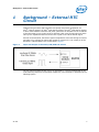
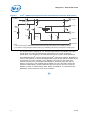
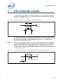
Intel® I/O Controller Hub (Intel® ICH) /
Platform Controller Hub (PCH) Family
Real Time Clock (RTC)
Electrical, Mechanical, and Thermal Specification (EMTS) - AP-728
April 2012
292276-009
INFORMATION IN THIS DOCUMENT IS PROVIDED IN CONNECTION WITH INTEL PRODUCTS. NO LICENSE, EXPRESS OR IMPLIED, BY ESTOPPEL OR
OTHERWISE, TO ANY INTELLECTUAL PROPERTY RIGHTS IS GRANTED BY THIS DOCUMENT. EXCEPT AS PROVIDED IN INTEL'S TERMS AND CONDITIONS
OF SALE FOR SUCH PRODUCTS, INTEL ASSUMES NO LIABILITY WHATSOEVER AND INTEL DISCLAIMS ANY EXPRESS OR IMPLIED WARRANTY, RELATING
TO SALE AND/OR USE OF INTEL PRODUCTS INCLUDING LIABILITY OR WARRANTIES RELATING TO FITNESS FOR A PARTICULAR PURPOSE,
MERCHANTABILITY, OR INFRINGEMENT OF ANY PATENT, COPYRIGHT OR OTHER INTELLECTUAL PROPERTY RIGHT.
A "Mission Critical Application" is any application in which failure of the Intel Product could result, directly or indirectly, in personal injury or death.
SHOULD YOU PURCHASE OR USE INTEL'S PRODUCTS FOR ANY SUCH MISSION CRITICAL APPLICATION, YOU SHALL INDEMNIFY AND HOLD INTEL AND
ITS SUBSIDIARIES, SUBCONTRACTORS AND AFFILIATES, AND THE DIRECTORS, OFFICERS, AND EMPLOYEES OF EACH, HARMLESS AGAINST ALL
CLAIMS COSTS, DAMAGES, AND EXPENSES AND REASONABLE ATTORNEYS' FEES ARISING OUT OF, DIRECTLY OR INDIRECTLY, ANY CLAIM OF PRODUCT
LIABILITY, PERSONAL INJURY, OR DEATH ARISING IN ANY WAY OUT OF SUCH MISSION CRITICAL APPLICATION, WHETHER OR NOT INTEL OR ITS
SUBCONTRACTOR WAS NEGLIGENT IN THE DESIGN, MANUFACTURE, OR WARNING OF THE INTEL PRODUCT OR ANY OF ITS PARTS.
Intel may make changes to specifications and product descriptions at any time, without notice. Designers must not rely on the absence or
characteristics of any features or instructions marked "reserved" or "undefined". Intel reserves these for future definition and shall have no
responsibility whatsoever for conflicts or incompatibilities arising from future changes to them. The information here is subject to change without notice.
Do not finalize a design with this information.
The products described in this document may contain design defects or errors known as errata which may cause the product to deviate from published
specifications. Current characterized errata are available on request.
Contact your local Intel sales office or your distributor to obtain the latest specifications and before placing your product order.
Code names featured are used internally within Intel to identify products that are in development and not yet publicly announced for release.
Customers, licensees and other third parties are not authorized by Intel to use code names in advertising, promotion or marketing of any product or
services and any such use of Intel's internal code names is at the sole risk of the user.
Intel and the Intel logo are trademarks of Intel Corporation in the U.S. and other countries.
*Other names and brands may be claimed as the property of others.
Copyright © 2012, Intel Corporation. All rights reserved.
2
AP-728
Contents
1
Background – External RTC Circuit.................................................................................. 5
2
RTC External Battery Connection .................................................................................... 9
3
RTC External Circuit .................................................................................................... 10
3.1
RTC External Capacitor Values ............................................................................ 11
3.2
RTC Signals ...................................................................................................... 12
3.2.1 Signals on RTCX1 and RTCX2 Pins ............................................................ 12
3.2.2 VBIAS................................................................................................... 14
3.2.3 SUSCLK ................................................................................................ 14
3.3
RTC Accuracy ................................................................................................... 15
3.3.1 RTC Voltage .......................................................................................... 15
3.3.2 External Capacitance Load....................................................................... 15
3.3.3 RTC Circuit Layout Considerations ............................................................ 15
3.3.4 Environmental Conditions ........................................................................ 15
3.4
RTC Accuracy Determination and Frequency
Measurement Technique..................................................................................... 16
3.4.1 Using Timekeeping Baseline Device........................................................... 16
3.4.2 Using the Time Interval Analyzer .............................................................. 16
4
Influences Under Environmental Stress ......................................................................... 18
5
Optimizations for Stress Testing ................................................................................... 19
6
Conclusion................................................................................................................. 20
Figures
1
2
3
4
5
6
7
8
9
10
11
AP-728
Input and Output of the Intel® ICH/PCH RTC Circuit ....................................................... 5
Intel® ICH1/2/3 RTC External Circuit ............................................................................ 6
Intel® ICH4 RTC External Circuit .................................................................................. 6
Intel® ICH5/6/7/8 RTC External Circuit ......................................................................... 7
Intel® ICH9/ICH10/Intel® 5 Series Chipset and Intel® 3400 Series Chipset
RTC External Circuit7
Intel® C200 Series Chipset and later Client Platform Controller Hubs (PCHs) ...................... 8
External and Internal Circuitry for the RTC Oscillator..................................................... 10
Clock Input Connection to X1, X2 Pins When Not Using Internal RTC ............................... 10
Example OP-Amp Configuration ................................................................................. 13
Screen-Capture of RTCX1 and RTCX2 Signals on Scope ................................................. 13
TIA Menu ................................................................................................................ 17
3
Revision History
Document #
Rev.
292276
001
Draft/Changes
Date
• Initial Release
March 2001
002
• General updates
August 2001
003
• ICH4 updates
May 2002
004
• ICH5 updates
June 2003
005
• ICH6 update. Also changed RTCRST# RC for ICH4-6
June 2004
006
• ICH7 update.
April 2005
007
• ICH8 update
May 2006
008
• ICH9 update
September 2007
Intel®
009
Intel®
• ICH10 /
5 Series Chipset and
3400 Series
Chipset / Intel® C200 Series Chipset and later Client PCHs
update
April 2012
§§
4
AP-728
Background – External RTC Circuit
1
Background – External RTC
Circuit
Chipsets using an Intel® I/O Controller Hub (Intel® ICH) family component, an
Intel® 5 Series Chipset, an Intel® 3400 Series Chipset, an Intel® C200 Series Chipset
or later client Platform Controller Hub (PCH) (referred to as ICH/PCH for the remainder
of this document) use a crystal circuit to generate a low-swing 32 kHz input sine wave.
This input is amplified and driven back to the crystal circuit via the RTCX2 signal.
Internal to the ICH/PCH, the RTCX1 signal is amplified to drive internal logic as well as
generate a free running full swing clock output for system use. This output pin of the
ICH/PCH is called SUSCLK. This is illustrated in Figure 1.
Figure 1.
Input and Output of the Intel® ICH/PCH RTC Circuit
The low-swing 32.768 kHz clock source is generated by a circuit implemented on the
motherboard (external to the ICH/PCH component). The schematic is illustrated in the
following figures:
AP-728
5
Background – External RTC Circuit
Figure 2.
Intel® ICH1/2/3 RTC External Circuit
VCCRTC
3.3V Sus
Schottky Diodes
1uF
1 KΩ
RTCX2
Vbatt
R1
10MΩ
32.768 KHz
Xtal
1 KΩ
RTCX1
C3
0.047uF
C1
C2
R2
10MΩ
VBIAS
VCCRTC, RTCX1, and RTCX2 are ICHn pins
VBIAS is used to bias the ICH1/2/3/4 Internal Oscillator
VCCRTC powers the RTC well of the ICHn
RTCX1 is the Input to the Internal Oscillator
RTCX2 is the feedback for the external crystal
Notes
Reference Designators Arbitrarily Assigned
3.3V Sus is Active Whenever System Plugged In
Vbatt is Voltage Provided By Battery
Figure 3.
Intel® ICH4 RTC External Circuit
3.3V Sus
VCCRTC
Schottky Diodes
1µF
0.1µF
RTCX2
1 KΩ
20 KΩ
Vbatt
R1
10MΩ
32.768 KHz
Xtal
RTCX1
C3
0.047 µF
1.0 µF
C1
C2
R2
10MΩ
RTCRST#
VBIAS
Notes:
The circuit changes from ICH3 are as follows:
1. For VccRTC and VBIAS, the use of one 1KΩ resistor near the coin battery instead of two 1KΩ resistors.
2. The use of a 0.1µF decoupling capacitor near the ball of VccRTC.
3. The original 1µF capacitor moved near the coin battery after the diode.
6
AP-728
Background – External RTC Circuit
Figure 4.
Intel® ICH5/6/7/8 RTC External Circuit
3.3V Sus
VCCRTC
Schottky Diodes
1uF
0.1uF
RTCX2
1 KΩ
20KΩ
Vbatt
R1
10MΩ
32.768 KHz
Xtal
RTCX1
C1
C2
1.0uF
RTCRST#
Note:
The circuit change from ICH4 is the external VBIAS circuit has been integrated into ICH5/6/7/8.
Figure 5.
Intel® ICH9/ICH10/Intel® 5 Series Chipset and Intel® 3400 Series Chipset
RTC External Circuit
3.3V Sus
VCCRTC
Schottky Diodes
1uF
0.1uF
RTCX2
1 KΩ
Vbatt
20 KΩ
20 KΩ
R1
10MΩ
32.768 KHz
Xtal
RTCX1
1.0 uF
1.0 uF
C1
C2
RTCRST#
SRTCRST#
Note: The circuit change from ICH8 is the addition of SRTCRST# implementation
AP-728
7
Background – External RTC Circuit
Figure 6.
Intel® C200 Series Chipset and later Client Platform Controller Hubs (PCHs)
VccDSW3_3
VCCRTC
1µF
Schottky Diodes
0.1µF
RTCX2
1 KΩ
20 KΩ
20 KΩ
32.768 KHz
Xtal
R1
10MΩ
Vbatt
RTCX1
1.0 µF
1.0 µF
C1
C2
RTCRST#
SRTCRST#
Notes:
1. The circuit change from Intel® 5 Series Chipset and Intel® 3400 Series Chipset is the VccDSW3_3 input pin
2. For platforms not supporting Deep S4/S5 / Deep Sx, the VccDSW3_3 pins will be connected to the VccSus3_3 pins.
The crystal network employs R1, C1, and C2 to generate the 32.768 kHz sine wave.
Actual values for these components are dependent on the crystal component
specification, trace lengths on the motherboard, and the crystal’s load capacitance.
For ICH9/ICH10/Intel® 5 Series Chipset and Intel® 3400 Series Chipset, SRTCRST# is
used to reset portions of the Intel® Management Engine (Intel® ME) and should not be
connected to a jumper or button on the platform. The only time this signal gets
asserted (driven low in combination with RTCRST#) should be when the coin cell
battery is removed or not installed and the platform is in the G3 state. Pulling this
signal low independently (without RTCRST# also being driven low) may cause the
platform to enter an indeterminate state. Similar to RTCRST#, it is imperative that
SRTCRST# not be pulled low in the S0 to S5 states.
§§
8
AP-728
RTC External Battery Connection
2
RTC External Battery
Connection
The RTC module requires an external battery connection to maintain its functionality
and its RAM while the ICH/PCH is not powered by the system.
The recommended batteries are: Duracell 2032, 2025, or 2016, which can give many
years of operation.
Batteries are rated by storage capacity. The battery life can be calculated by dividing
the capacity by the average current required. For example, if the battery storage
capacity is 170 mAh (assumed usable) and the average current required is 5 μA, the
battery life will be at least:
170,000 μAh / 5 μA = 34,000 h = 3.88 years.
The voltage of the battery can affect the RTC accuracy. VccRTC must be greater than
the min voltage specification at all times to ensure the accuracy of the RTC clock and
correctly storing RTC SRAM data. Please refer to specific component datasheet for
VccRTC min voltage value.
The battery must be connected to the ICH/PCH via isolation diode circuit. The diode
circuit allows the ICH/PCH’s RTC-well to be powered by the battery when the system
power is not available, but by the system power when it is available. To do this, the
diodes are set to be reverse biased when the system power is not available. Figure 2,
Figure 3, and Figure 4 have the example of a diode circuitry that is used.
As noted, a standby power supply should be used in desktop and mobile system to
provide continuous power to the RTC when available, which will significantly increase
the RTC battery life.
§§
AP-728
9
RTC External Circuit
3
RTC External Circuit
The ICH/PCH module requires an external oscillating source of 32.768 kHz connected
on RTCX1 and RTCX2 pins. Figure 7 represents the internal and external circuitry that
comprise the oscillator of the RTC.
Figure 7.
External and Internal Circuitry for the RTC Oscillator
Internal
X1
C1
10M
X2
External
C2
C1, C2 are the required external capacitors that affect the accuracy of the RTC. Choose
the right capacitor value for C1 and C2, and the tolerance should be less than or equal
to 5%; both are important to maintain RTC accuracy. Section 3.1 presents some
guidelines for choosing these values.
Note:
Even if the ICH/PCH internal RTC is not used, it is still necessary to supply clock input
to X1 of the ICH/PCH because other signals are gated off that clock in suspend modes.
In this case, an oscillator or a single clock input can be used to drive into X1 with X2
left as no connect; please refer to specific component datasheet for RTC X1 input
voltage max value. Figure 8 illustrates the connection. However, this is not a validated
or supported configuration.
Figure 8.
Clock Input Connection to X1, X2 Pins When Not Using Internal RTC
Internal
X1
32 KHz
10
X2 External
10M
No Connection
AP-728
RTC External Circuit
3.1
RTC External Capacitor Values
To maintain the RTC’s accuracy, the external capacitor values should be chosen to
provide the manufacturer’s specified load capacitance (Cload) for the crystal when
combined with the parasitic capacitance of the circuits traces, socket (if used),
package, and ICH/PCH input capacitances. The following equation can be used to
choose the external capacitance values:
Cload = [(C1 + Cin1 + Ctrace1)*(C2 + Cin2 + Ctrace2)]/[(C1 + Cin1 + Ctrace1 +
C2 + Cin2 + Ctrace2)] + Cparasitic
Where:
• Cload = Crystal’s load capacitance. This value can be obtained from Crystal’s
specification.
• Cin1, Cin2 = input capacitances at RTCX1, RTCX2 pins of the ICH/PCH. These values
can be obtained in the ICH/PCH’s data sheet.
• Ctrace1, Ctrace2 = Trace length capacitances measured from the Crystal terminals to
RTCX1, RTCX2 pins. These values depend on the characteristics of board material,
the width of signal traces and the length of the traces. The typical value of this
capacitance is approximately equal to:
Ctrace ≈ trace length * 2 pF/inch
• Cparasitic = Crystal’s parasitic capacitance. This capacitance is created by the
existence of electrode plates and the dielectric constant of the crystal blank inside
the crystal part. Refer to the crystal’s specification to obtain this value.
Ideally, C1 and C2 can be chosen such that C1 = C2. Using the equation of Cload above,
the value of C1/C2 can be calculated to give the best accuracy (closest to 32.768 kHz)
of the RTC circuit at room temperature. However, C2 can be chosen such that C2 > C1.
Then C1 can be trimmed to obtain 32.768 kHz.
In certain conditions, both C1/C2 values can be shifted away from the theoretical
values (calculated values from the above equation) to obtain the closest oscillation
frequency to 32.768 kHz. When C1 and C2 values are smaller then the theoretical
values, the RTC oscillation frequency will be higher.
The following example will illustrates the use of the practical values for C1 and C2, in
the case that theoretical values can not ensure the accuracy of the RTC in a low
temperature condition:
Example 1:
According to a required 12 pF load capacitance of a typical crystal that is used with the
ICH/PCH, the calculated values of C1 = C2 is 18 pF at room temperature (25 °C) to
yield a 32.768 kHz oscillation.
At 0 °C the frequency stability of crystal gives –23 ppm (assumed that the circuit has 0
ppm at 25 °C). This makes the RTC circuit oscillate at 32.767246 kHz instead of 32.768
kHz.
If the values of C1 and C2 are chosen to be 6.8 pF instead of 18 pF, this will make the
crystal oscillate at a higher frequency at room temperature (+23 ppm) but this
configuration of C1 and C2 makes the circuit oscillate closer to 32.768 kHz at 0 °C. The
6.8 pF value of C1 and C2 is the practical value.
AP-728
11
RTC External Circuit
Note that the temperature dependency of crystal frequency is a parabolic relationship
(ppm / degree squared). The effect of the crystal’s frequency when operating at 0 °C
(25 °C below room temperature) is the same when operating at 50 °C (25 °C above
room temperature).
The values of C1 and C2, calculated from the equation above are only the theoretical
values. Ideally, these values will be the same as practical values. However, the values
of C1 and C2 should be chosen based on the values that give the best accuracy of the
RTC circuit. In every specific board design, these practical values may be slightly
different from theoretical values.
3.2
RTC Signals
3.2.1
Signals on RTCX1 and RTCX2 Pins
The RTC oscillation signal is a sinusoidal signal that provides a 32.768 kHz frequency to
the ICH/PCH. This is a small analog signal with peak-to-peak voltage about 200 mV–
500 mV. The voltage swing on RTCX2 will be slightly larger than the voltage swing on
RTCX1, since RTCX2 signal is amplified through the internal inverter of the ICH/PCH.
The RTC circuit oscillates with extremely low bias current (refer to specific component
datasheet for IccRTC maximum value); therefore, this signal is very sensitive to the
environmental conditions such as board residue (solder flux, dust), humidity, etc. For
example, touching directly on this circuit may cause leakage that can completely
attenuate the oscillation signal and make the RTC oscillation stop.
Measuring RTCX1 and RTCX2 is accomplished only by using the following technique to
minimize any measurement equipment loading effects.
1. Configure an Analog Devices AD823* (AD823AN) or equivalent Op Amp with very
high input impedance (on the order of 10E12 – 10E14), as a unity gain follower as
shown below. Note: This may be different depending on the Op-Amp used. See
Figure 9 for an illustration.
2. The conductor between the signal being measured and the Op Amp input must be
less than 4 mm with a direct connection preferable. The VS+ must be connected to
a voltage source that is on all the time, such as an external supply or a 9 V battery.
3. Collect the RTC electrical characteristics:
a.
12
Place an oscilloscope probe with sufficient ground reference on the Op-Amp
output. The oscilloscope should be configured for 100 mV/DIV and 20 µs/DIV
with a trigger set to approximately 200 mV, or until capture is obtained. Record
the RTCX1 Vpp. Optional data can be captured such as: DC Offset of RTCX1 and
2 Vpp of RTCX2, DC level for VBIAS, and IccRTC.
AP-728
RTC External Circuit
Figure 9.
Example OP-Amp Configuration
AD822AR-3V Op-Amp configured for "unity gain"
+VS => 3 V
VS+
Connect to Oscilloscope
–
To RTCX1
RTCX2 or VBIAS
+
VS–
Figure 10 shows an example of a screen capture on the RTCX1 and RTCX2 signals:
Figure 10.
AP-728
Screen-Capture of RTCX1 and RTCX2 Signals on Scope
13
RTC External Circuit
3.2.2
VBIAS
The external VBIAS circuit is only required for ICH1/2/3/4. All other platforms have
integrated the external VBIAS circuit.
For ICH1/2/3/4, VBIAS is a DC voltage level that is necessary for biasing the RTC
oscillator circuit. This DC voltage level is filtered out from the RTC oscillation signal by
the RC network of R2 and C3 (see Figure 2 and Figure 3). Therefore, it is a selfadjusted voltage. Board designers should not manually bias the voltage level on VBIAS.
Checking the VBIAS voltage level is used for testing purposes only to determine the
right bias condition of the RTC circuit.
VBIAS should be at least 200 mV DC on ICH1/2/3/4. The RC network of R2 and C3 will
filter out most of AC signal that exist on this pin, however, the noise on this pin should
be kept minimal in order to ensure the stability of the RTC oscillation.
Probing VBIAS requires the same technique as probing the RTCX1, RTCX2 signals
(using Op-Amp)
VBIAS is also very sensitive to environmental conditions.
3.2.3
SUSCLK
SUSCLK is a square wave-form signal output from the RTC oscillation circuit.
Depending on the quality of the oscillation signal on RTCX1 (largest voltage swing),
SUCCLK duty cycle can be between 30-70%. If the SUSCLK duty cycle is beyond 30%–
70% range, it indicates a poor oscillation signal on RTCX1 and RTCX2.
SUSCLK can be probed directly using a normal probe (50 Ω input impedance probe)
and is the appropriate signal to check the RTC frequency to determine the accuracy of
the ICH/PCH’s RTC Clock (see Section 3.4.2 for details).
14
AP-728
RTC External Circuit
3.3
RTC Accuracy
The ICH/PCH RTC circuit is a low current circuit designed to provide accurate time
keeping service, at an extremely low current consumption (IccRTC) a maximum of 5 or
6 μA (please refer to specific component datasheet for IccRTC max value). As a result,
this circuit is subject to adverse influences, which must be addressed or understood to
ensure the best possible RTC accuracy.
The RTC accuracy can be affected by the following primary factors:
3.3.1
RTC Voltage
The RTC accuracy can be affected by the voltage of battery. In general, when the
battery voltage decays, the RTC accuracy also decreases. High accuracy (less than ±10
ppm which does not include Crystal’s tolerance) can be obtained when VccRTC is larger
than the min voltage specification. For example: 20 ppm is equivalent with 1.728 sec
error in one day.
PPM = ((Fo – 32.7680) / 32.768) * 10^6
1 day = 24 hours/day * 60 min/hour * 60 sec/min = 86400 sec
20 ppm * 1 day (86400 sec) = (20 * 86400) / 1000000 = 1.728 sec
3.3.2
External Capacitance Load
The external capacitance load values are combined with the external capacitor values,
the capacitance of the circuit’s trace, socket, and package. These values should be
matched to the actual load capacitance required of the crystal used for the RTC
accuracy. Refer to Section 3.1 for guidelines to calculate the external capacitance.
3.3.3
RTC Circuit Layout Considerations
Since the RTC circuit is very sensitive and requires high accuracy oscillations,
reasonable care must be taken during the layout and routing of the RTC circuit. Some
recommendations are:
• Reduce trace capacitance by minimizing the RTC trace length. The ICH/PCH
requires a trace length less than 1 inch on each branch (from crystal’s terminal to
RTCXn pin). Routing the RTC circuit should be kept simple to reduce the trace
length measurement and increase accuracy on calculating trace capacitances. Trace
capacitance depends on the trace width and dielectric constant of board’s material.
On FR-4, a 5-mil trace has approximately 2 pF per inch.
• Trace signal coupling must be reduced. Avoid routing noisy periodic signals close
and parallel to RTCX1, RTCX2, and VBIAS.
• Ground referencing is highly recommended.
3.3.4
Environmental Conditions
The crystal temperature itself will impact the RTC accuracy. The deviation from room
temperature will reduce the RTC accuracy unless this factor is compensated by using
the practical configuration of C1, C2 value (See Section 3.1 for details).
Condensation from humidity can also affect the RTC accuracy due to leakage on RTC
signals (see Section 3.2 for details).
Note:
AP-728
Heat will damage the crystal when reworking the boards. Follow the specification of the
crystal to set the right temperature for operation.
15
RTC External Circuit
3.4
RTC Accuracy Determination and Frequency
Measurement Technique
The accuracy of RTC clock can be determined by many different methods. Two common
methods for checking RTC accuracy are:
• Using timekeeping-baseline-device (via BIOS and system NVRAM)
• Using Time-Interval-Analyzer on SUSCLK signal
3.4.1
Using Timekeeping Baseline Device
Accuracy of the baseline device is crucial to determining RTC accuracy. The use of a
watch or clock is not sufficiently accurate for 25 ppm range accuracy over the periods
used during these tests. It is required that a Global Positioning System device (GPS) be
used instead. A GPS contains a clock that is reset at acquisition time to an extremely
accurate time. Over time though, the GPS time will drift like any other clock. For this
reason the GPS should be reset, powered on outside and allowed to synchronize, within
15 minutes of either setting time on motherboard or using it for a standard readout.
3.4.2
Using the Time Interval Analyzer
Using an Agilent* TIA (Time Interval Analyzer) or the equivalent is a very accurate way
of measuring the RTC frequency. This tool can measure the 32.768 kHz frequency of
the RTC with a tolerance typically less than ± 20 mHz (mili-Hertz).
It is ideal to use this equipment to determine the configurations of the fork tuning
capacitors C1 and C2 which are described in Section 3.1. This is to get the most
accurate frequency on the RTC circuit.
The following is a description of how to use an Agilent TIA to calculate the frequency of
the RTC circuit:
1. The frequency of RTC oscillator can be monitored on the SUSCLK signal of the ICH/
PCH. Locate SUSCLK signal on the board and connect this signal to the probe of
Agilent-TIA with a properly connected ground pin.
2. Run the Agilent-E1743A program. Target frequency should be set to 32.768
kHz.(Refer to Agilent TIA user manual for more information on how to setup the
equipment.)
3. On TIA menu, click on “Measure/View Setup,” the setup dialog box will appear as
shown in Section 11
16
AP-728
RTC External Circuit
Figure 11.
TIA Menu
The pacing number is the number of clock edges that the TIA will count before it
capture for each time stamp. Depending on the TIA memory size, the number of
samples varies (1024, 4096, etc.), chose the largest number possible. The measured
frequency (F0) will be calculated based upon the average period of all samples. This is
the frequency of the RTC clock. The following formula is used to calculate the PPM:
PPM = [ |(F0 – 32.768 kHz)| / (32.768 kHz)] * 10E6
§§
AP-728
17
Influences Under Environmental Stress
4
Influences Under
Environmental Stress
Crystal Characteristics: Typical 32.768 kHz crystals have an operating temperature
ceiling of 60 °C, thus limit the test temperature accordingly. In addition, the
temperature coefficient of these crystals can cause time-loss of approximately 3 sec/
day at 60 °C.
Fork Capacitor Tuning: The timekeeping of the RTC is dependent on the RTCX1 input
voltage swing. Oscillation that is marginal may result in failure to meet Vih of this input
and thus “ticks” of the clock may be missed resulting in time-loss. Optimum Vpp of this
RTCX1 signal is achieved by accurately matching the crystal’s C-load specification
(typically 12 pF).
Board Leakage: Since this circuit operates at such low current, it is very sensitive to
sources of leakage on the motherboard. Manufacturing residue can cause leakage as
well as condensation on the board encountered during temperature and/or humidity
testing.
Timekeeping Baseline Device: Time of motherboards is typically compared to a
baseline device, like a watch or other baseline clock device believed to be accurate. The
case is that most timekeeping devices like this are not sufficiently accurate. This can
cause an additional source of error.
§§
18
AP-728
Optimizations for Stress Testing
5
Optimizations for Stress
Testing
To obtain the best RTC accuracy in environmental stress conditions, the above listed
factors can be optimized. While there is little that can be done to change crystal
characteristics, there are opportunities to maximize the oscillator voltage swing and to
minimize board leakage; described below:
Fork Capacitor Tuning: The fork capacitors (C1/C2) must be chosen to provide the
greatest Vpp (of RTCX1) yet still providing the best accuracy. This is typically
accomplished by laboratory analysis and is specific to each motherboard (see Section
3.1 for details). Analysis of several motherboards has shown that 18 pF is optimum for
many designs. This analysis is accomplished by monitoring SUSCLK accuracy with
extremely sensitive measurement equipment that can measure frequency to a PPM
range of less than 2 ppm. The SUSCLK output is monitored (and IccRTC may be
monitored) for various configurations of fork caps. All this can be accomplished at
room/ambient conditions. The goal is to obtain a capacitor choice that provides
greatest Vpp and the best accuracy.
Board Leakage: Care must be taken to ensure that there is no manufacturing residue
left on the motherboard when performing environmental stress testing. Consider a
solder paste containing less flux which is an organic acid that becomes conductive in
moisture. Ensure cleaning after the solder process, especially for water soluble flux.
Pay careful attention to underneath discrete components of the RTC circuit and the
ICH/PCH package.
Another source of leakage is condensation which may occur on the motherboard during
an environmental stress test. This absolutely must be prevented. Choice of a noncondensing chamber profile can ensure that dew-points are not encountered. An
acceptable profile is listed below, showing both temperature and relative humidity
(%RH) requirements. There must be sufficient air flow in the chamber to prevent
temperature spots, which could also cause condensation. The key to preventing
condensation is not allowing temperature to ramp when the board is exposed to
humidity. As the air temperature rises, while there is moisture in the air, the board will
always be cooler than the air temperature thereby causing condensation.
Non-Condensing Temperature/Humidity Profile:
1. Hold at ambient (25 °C/25%RH) for 30 minutes.
2. Ramp temperature at a constant rate to a maximum of 60 °C over at least 30
minutes while maintaining 25%RH.
3. Ramp up %RH at a constant rate to a maximum of 85% over at least 2 hours while
maintaining temperature set in step 2.
4. Hold at sustained temp/RH for user defined time.
5. Ramp down %RH at a constant rate to 25% over at least 2 hours while maintaining
temperature set in step 2.
6. Ramp down temperature at a constant rate to 25 °C over at least 30 minutes while
maintaining 25% RH.
7. Jump back to Step 1 n times.
RTC Accuracy Determination Device: Use appropriate device to check the accuracy
of the RTC clock (see Figure 10).
§§
AP-728
19
Conclusion
6
Conclusion
The ICH/PCH’s RTC external oscillator is an extremely sensitive circuit because it
operates at a very small current. Care must be taken when working with this circuit.
To ensure the accuracy of the ICH/PCH RTC circuit for each specific board design and
RTC circuit layout, the external load capacitance should be optimized by choosing
correct values of the tuning fork capacitors C1/C2.
The occurrence of time-loss under environmental stress conditions is dependent on
motherboard factors (cleanliness, discrete component characteristics, layout, fork
capacitor values), and condensation. If time-loss is observed on your system, check all
of the sources of inaccuracy listed in this document to improve immunity of the internal
ICH/PCH oscillator to time loss.
§§
20
AP-728