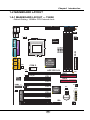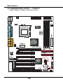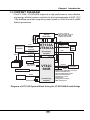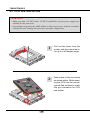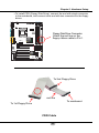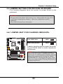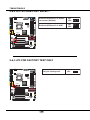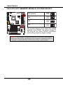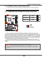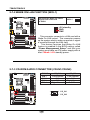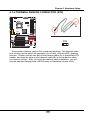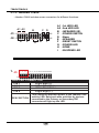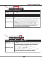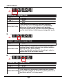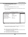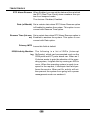
1
R
SL-75KAV/75KAV-X
USER MANUAL V 1.2
USER NOTICE
Product Model
Manual Revision
Release Date
: SL-75KAV/75KAV-X
: V1.2
: May 2001
his Users’ Guide & Technical Reference is to help system
manufacturers and end-users set up and install the mainboard.
T
Every effort has been made to ensure that the information in this
manual is accurate. Soltek Computer Inc. is not responsible for printing or clerical errors. Information in this document is subject to
change without notice and does not represent a commitment on the
part of Soltek Computer Inc.
No part of this manual may be reproduced, transmitted, translated
into any language in any form or by any means, electronic or
mechanical, including photocopying and recording, for any purpose
without the express written permission of Soltek Computer Inc.
Companies and products mentioned in this manual are for identification purpose only. Product names appearing in this manual may
or may not be registered trademarks or copyrights of their respective companies.
Soltek computer inc. Provides this manual “As is “ without warranty of any kind, either express or implied, including but not limited
to the implied warranties or conditions of merchantability or fitness
for a particular purpose. In no event shall Soltek computer inc. be
liable for any loss or profits, loss of business, loss of use or data,
interruption of business, or for indirect, special, incidental, or consequential damages of any kind, even if Soltek computer inc. has
been advised of the possibility of such damages arising from any
defect or error in this manual or product.
Copyright © 2001 Soltek Computer Inc. All Rights Reserved.
• AMD Athlon ThunderbirdTM, and DuronTM processors are trademarks of AMD Corporation.
• VIA, KT-133A, VT8363A and VT82C686B are trademarks of VIA Corporation.
SOLTEK AROUND THE WORLD
SOLTEK COMPUTER INC.
Address
Telephone
Fax
E-mail
Web site
: 7F, No. 306-3, Ta-Tung Rd, Sec.1, Hsi-Chih, TaipeiHsien, Taiwan, R.O.C.
: 886-2-2642-9060
: 886-2-2642-9065
: [email protected]
: http://www.soltek.com.tw
SOUL TECHNOLOGY EUROPE B.V.
Address
Telephone
Fax
E-mail
Web site
: Hongkongstraat 55, 3047 BR, Rotterdam, The
Netherlands
: 31-10-2457492
: 31-10-2457493
: [email protected]
: http://www.soultech-europe.com
75KAV/75KAV-X
CONTENT
Chapter 1
Introduction ............................................... 9
1-1 MAINBOARD SPECIFICATION .................................................. 10
1-1-1 PROCESSOR ................................................................................... 10
1-1-2 CHIPSET ........................................................................................... 10
1-1-3 ADVANCED HIGH PERFORMANCE DRAM CONTROLLER ........... 10
1-1-4 FULL FEATURED ACCELERATED GRAPHICS PORTS ................. 10
(AGP) CONTROLLER ................................................................. 10
1-1-5 MULTI-I/O FUNCTION ...................................................................... 10
1-1-6 EXPANSION SLOTS ......................................................................... 11
1-1-7 AWARD BIOS V6.0, SUPPORTING ................................................. 11
1-1-8 SOUND CONTROLLER .................................................................... 11
1-1-9 POWER MANAGEMENT .................................................................. 11
1-1-10 FORM FACTOR .............................................................................. 12
1-1-11 HARDWARE MONITORING ........................................................... 12
1-1-12 OTHERS ......................................................................................... 12
1-2 MAINBOARD LAYOUT ............................................................... 13
1-2-1 MAINBOARD LAYOUT --- 75KAV ..................................................... 13
1-2-2 MAINBOARD LAYOUT --- 75KAV-X ................................................. 14
1-3 CHIPSET DIAGRAM ................................................................... 15
Chapter 2
Hardware Setup ...................................... 17
2-1 CPU INSTALLATION ..................................................................
2-2 MEMORY INSTALLATION ..........................................................
2-3 ACCELERATED GRAPHICS PORT(AGP) PRO INSTALLATION .....
2-4 HDD/FDD INSTALLATION ..........................................................
2-5 SWITCH SETTING FOR CPU FREQUENCY AND VOLTAGE ...
18
19
21
22
24
2-5-1 INFORMATION ON AMD SOCKET 462 PROCESSOR ................... 24
2-5-2 CPU EXTERNAL FREQUENCY SETTING (BY SW1) ...................... 25
2-5-3 BUS RATIO SELECT (BY SW2 DIP1-4/JP17) .................................. 26
2-6 JUMPER SETTING FOR DEVICES ON BOARD: ...................... 27
4
Content
2-6-1 JUMPER JBAT1 FOR CLEARING CMOS DATA: ............................. 27
2-6-2 JP1/JP2 USB PORT SELECT ........................................................... 28
2-6-3 JP3 FOR FACTORY TEST ONLY ..................................................... 28
2-6-4 JP7 POWER LOST RESUME ........................................................... 29
2-6-5 JP9 USB WAKE UP .......................................................................... 29
2-6-6 JP10/JP11 MEMORY MODULE VOLTAGE SELECT ....................... 30
2-7 CONNECTORS CONFIGURATIONS ......................................... 31
2-7-1 ONBOARD FAN CONNECTOR (FAN1/FAN2/FAN3) ........................ 31
2-7-2 WAKE ON LAN FUNCTION (WOL1) ................................................ 32
2-7-3 CD-ROM AUDIO CONNECTOR (CD-IN1/CD-IN2) ........................... 32
2-7-4 THERMAL SENSOR CONNECTOR (RT2) ....................................... 33
2-7-5 HEADER J3&J4 ............................................................................... 34
2-7-6 CHASSIS PANEL CONNECTOR ..................................................... 37
2-7-7 ATX POWER SUPPLY CONNECTOR ............................................. 38
2-7-8 PS/2 MOUSE AND PS/2 KEYBOARD ............................................. 38
2-7-9 SERIAL PORT CONNECTOR .......................................................... 39
2-7-10 SECOND USB HEADER (USB2) ................................................... 40
2-7-11 IRQS DESCRIPTION FOR VARIOUS DEVICES ............................ 41
2-8 VOICE DIAGNOSTIC FUNCTION----ONLY FOR 75KAV-X ........ 42
2-8-1 VOICE DIAGNOSTIC FUNCTION SELECT (BY JP4/JP5) ............... 43
2-8-2 VD-TECH CONTROLLER CHIP (BY JP8) ........................................ 43
Chapter 3
Software Setup ....................................... 45
ABOUT SUPPORT CD .....................................................................
3-1 VIA CHIPSET DRIVER INSTALLATION (4-IN-1 DRIVER) .........
3-2 AC97 AUDIO CODEC DRIVER INSTALLATION ........................
3-3 HARDWARE MONITOR INSTALLATION ...................................
Chapter 4
45
46
49
51
BIOS Setup .............................................. 55
THE BIOS .........................................................................................
4-1 WHAT IS BIOS SETUP ...............................................................
4-2 HOW TO RUN BIOS SETUP ......................................................
4-3 WHAT IS CMOS .........................................................................
4-4 WHAT IS POST ..........................................................................
5
55
56
56
56
56
75KAV/75KAV-X
4-5 BIOS UPGRADE ......................................................................... 56
4-5-1 BEFORE UPGRADING BIOS ........................................................... 57
4-5-2 UPGRADE PROCESS ...................................................................... 57
4-6 BIOS SETUP°XCMOS SETUP UTILITY .................................... 61
4-6-1 STANDARD CMOS SETUP .............................................................. 62
4-6-2 ADVANCED BIOS FEATURES ......................................................... 65
4-6-3 ADVANCED CHIPSET FEATURES .................................................. 70
4-6-4 INTEGRATED PERIPHERALS ......................................................... 75
4-6-5 POWER MANAGEMENT SETUP ..................................................... 79
4-6-6 PNP / PCI CONFIGURATION ........................................................... 86
4-6-7 SMARTDOC ANTI-BURN SHIELD ................................................... 90
4-6-8 FREQUENCY/VOLTAGE CONTROL ................................................ 93
4-6-9 LOAD OPTIMIZED DEFAULTS ......................................................... 94
4-6-10 SET SUPERVISOR / USER PASSWORD ...................................... 96
4-6-11 SAVE & EXIT SETUP ...................................................................... 97
4-6-12 EXIT WITHOUT SAVING ................................................................ 97
Appendices .................................................................... 98
APPENDICES-1 TECHNICAL TERMS INTRODUCTION ............... 99
APPENDICES-2 IDENTIFYING BIOS VERSION AND .................. 100
BIOS PART NUMBER ........................................ 100
APPENDICES-3 IDENTIFYING MAINBOARD \ MODEL .............. 102
NUMBER ............................................................. 102
6
Content
MEMO
7
75KAV/75KAV-X
ITEMLIST CHECKUP
Mainboard
Support CD
User’s Manual
Bundled Bonus Pack CD
Bundled Bonus Pack Manual
Temperature Sensor Cable
ATA66/100 IDE Cable
RS232 Cable
FDD Cable
8
Chapter1 Introduction
CHAPTER
1
INTRODUCTION
• This chapter briefly introduces the characteristics of this mainboard. It
includes the information regarding the chipset, CPU types, built-in
functions and layout. Users will have more ideas about mainboards after
reading this chapter.
THIS CHAPTER CONTAINS THE FOLLOWING TOPICS :
N J N=MAINBOARD SPECIFICATION
N J O=MAINBOARD LAYOUT
N J P=CHIPSET DIAGRAM
9
75KAV/75KAV-X
1-1 MAINBOARD SPECIFICATION
1-1-1 PROCESSOR
• Supporting AMD Athlon Thunderbird processors up to 1.5GHz.
• Supporting AMD Athlon Duron processors up to 1.2GHz.
• Supporting processor VID (voltage ID) and FID (frequency ID) auto detection.
• Supporting AMD Athlon processor with 200 and 266MHz Front Side bus.
1-1-2 CHIPSET
• North Bridge VIA VT8363A (KT-133A) system controller High Performance
Athlon CPU Interface.
• South Bridge VIA VT82C686B.
1-1-3 ADVANCED HIGH PERFORMANCE DRAM
CONTROLLER
• Supporting PC133 and PC100 SDRAM and Virtual Channel Memory (VCM)
SDRAM up to 3 DIMMs.
• 64-bit data width and 3.3V DRAM interface.
• Supporting up to 1.5 GB memory space.
• Supporting Different DRAM types used in mixed combinations.
• PCI-2.2 compliant, 32 bit 3.3V PCI interface with 5V tolerant inputs.
1-1-4 FULL FEATURED ACCELERATED GRAPHICS PORTS
(AGP) CONTROLLER
• Synchronous and pseudo-synchronous with the host CPU bus with optimal
skew control PCI AGP Mode 33MHz/66MHz/100MHz DDR 3x synchronous.
• Supporting 66MHz 1x, 2x and 4x modes for AD and SBA signaling.
• AGP v2.0 compliant.
1-1-5 MULTI-I/O FUNCTION
• Two UARTs for complete Serial Ports.
• One dedicated IR connector supporting:
--A third serial port dedicated to IR function either through the two complete serial
ports or the third delicated port Infrared-IrDA (HPSIR) and ASK( Amplitude Shift
Keyed) IR.
• Multi-mode parallel connector supporting:
10
Chapter1 Introduction
--Standard mode, ECP and EPP.
• Floppy Disk connector supporting:
--Two FDDs with drive swap function.
• Universal Serial Bus connector supporting:
--USB v1.1 and Intel Universal HCI v1.1 compatible.
--2 built-in USB connectors, in addition to one internal USB header which requires
a USB cable to support 2 more optional USB ports.
• PS/2 keyboard connector.
• PS/2 Mouse connector.
1-1-6 EXPANSION SLOTS
• Five PCI bus Master slots.
• One ISA slot.
• One AGP Pro 4x mode slot.
• Three DIMM slots.
1-1-7 AWARD BIOS V6.0, SUPPORTING
• Plug & Play V1.0.
• Flash Memory for easy upgrade.
• Year 2000 compliant.
• BIOS writing protection.
• SMARTDOC ANTI-BURN SHIELD.
• RedStorm Overclocking Tech.
1-1-8 SOUND CONTROLLER
• SoundBlaster Pro Hardware and Direct Sound Ready AC97 Digital Audio
Controller with Codec onboard.
1-1-9 POWER MANAGEMENT
• ACPI 1.0 compliant (Advanced Configuration and Power Interface).
• APM V1.2 compliant (Advanced power management).
• Supporting ACPI suspend STR mode (Suspend To RAM) and POS mode
(Power On Suspend).
• Supporting Wake On LAN (WOL) & Wake On Modem.
• Supporting real time clock (RTC) with date alarm, month alarm, and century field.
11
75KAV/75KAV-X
• Supporting USB boot-up Function.
1-1-10 FORM FACTOR
• ATX form factor, 4 layer PCB.
• Mainboard size: 22.0cm x 30.5cm.
1-1-11 HARDWARE MONITORING
• Programmable control, status, to provide monitoring and alarm for flexible
desktop management of hardware temperature. (software included in support CD)
• 5 positive voltage statuses monitoring.
• 2 temperature statuses monitoring.
• 2 fan speeds statuses monitoring.
1-1-12 OTHERS
• Clock generator supporting 1 MHz linear clock setting.
12
Chapter1 Introduction
1-2 MAINBOARD LAYOUT
1-2-1 MAINBOARD LAYOUT --- 75KAV
• Default Setting: 100MHz CPU External clock.
upper
upper
PS/2
USB0
MOUSE
lower
lower
PS/2
USB1
K/B
FAN1
5 4 3 2 1
DIP
ATX POWER
4 3 2 1
ON
DIP
SW1
JP10
3
1
1
SOCKET A
GAME/MIDI PORT
3
3
JP11
Clock
Generator
FAN3
FDD1
DIMM1
DIMM2
DIMM3
COM 1
LPT1
LINE
OUT
3
JP17
JP9
LINE
IN
SSF1
1
1
MIC
ON
SW2
VIA
KT-133A
VT8363A
COM 2
10
JP3
1
AGP PRO 4X
ZD1
IDE1
1
1
4
4
CD_IN2
CD_IN1
PCI 1
AC'97
Codec
IDE2
3
PCI 2
J3
J4
15
T/LED
SMI
PWR/LED
PWR
3
15
JBAT1
1
ISA
W5280
13
RST
FAN2
SPK
Li
Battery
PCI 5
+
-
PCI 4
RT2
IR
WOL1
FLASH BIOS
1
VIA
VT82C
686B
1
JP7
PCI 3
HDD/LED
3 JP1
3 JP2
+ - - +
1
1
1
16
1
USB2
75KAV/75KAV-X
1-2-2 MAINBOARD LAYOUT --- 75KAV-X
• Default Setting: 100MHz CPU External clock.
upper
upper
PS/2
USB0
MOUSE
lower
lower
PS/2
USB1
K/B
FAN1
5 4 3 2 1
DIP
ATX POWER
4 3 2 1
ON
DIP
SW1
ON
1
JP10
3
1
1
JP9
SOCKET A
GAME/MIDI PORT
3
3
JP11
Clock
Generator
FAN3
FDD1
DIMM1
DIMM2
DIMM3
COM 1
LPT1
LINE
OUT
LINE
IN
3
JP17
1
MIC
SSF1
SW2
VIA
KT-133A
VT8363A
COM 2
10
1
JP3
AGP PRO 4X
ZD1
IDE1
1
1
4
4
CD_IN2
CD_IN1
PCI 1
AC'97
Codec
IDE2
1
15
15
J3
J4
3 JP4
3 JP5
3 JBAT1
SMI
RST
IR
Li
Battery
1
W5280
W5280
14
3
FAN2
SPK
JP8
ISA
HDD/LED
PCI 5
+
-
PCI 4
RT2
1
1
1
T/LED
FLASH BIOS
WOL1
VIA
VT82C
686B
PWR
PCI 3
PWR/LED
3 JP1
3 JP2
+ - - +
1
1
1
1
16
1
USB2
JP7
3
PCI 2
Chapter1 Introduction
1-3 CHIPSET DIAGRAM
CFWDRST
PROCRDY
CONNECT
• The KT-133A / VT82C686B chipset is a high performance, cost-effective
and energy efficient system controller for the implementation of AGP / PCI
/ ISA desktop personal computer system based on 64-bit Socket-A (AMD
Athlon) processors.
GCLK
3D Graphics
Controller
AGP Bus
GCKRUN#
PCKRUN#
PCLK
PCI Bus
Athlon
Host CPU
Address
Out
SYSCLK, SYSCLK#
INTR, NMI, SMI#, STPCLK#,
IGNNE#, FERR#, A20M#,
PWROK, INIT#, RESET#
Data
In
CKE
Memory Bus
KT133A
VT8363A
North Bridge
552 BGA
MCLK
SDRAM
Clock
Buffer
HCLK
PCLK
SUSCLK,
SUSST1#
BIOS ROM
ATA 33/66/100
USB Ports 0 - 3
AC97 Audio Codec
AC97 Link
VT82C
686B
ISA Bus
RTC Crystal
South Bridge
352 BGA
CPUSTP#
PCISTP#
Clock
Generator
SMBus
Power Plane & Peripheral Control
GPIO and ACPI Events
Hardware Monitoring Inputs
Keyboard / PS2 Mouse
Serial Ports 1 and 2
Parallel Port
Floppy Drive Interface
MIDI / Game Ports
Diagram of KT133A System Block Using the VT82C686B South Bridge
15
75KAV/75KAV-X
MEMO
16
Chapter2 Hardware Setup
CHAPTER
2
HARDWARE SETUP
ATTENTION !!!
1. Please refer to your processor installation or other
documentation attached with your CPU for more
detailed installing instruction.
2. Installing a heat sink and cooling fan is necessary for
proper heat dissipation from your CPU. Incorrect
installation may result in overheating and damage of
your CPU.
3. Before changing the setting of CPU Vcore from BIOS
program, user SHOULD make sure of correct specification both of CPU CLOCK and RATIO. Incorrect setting may cause damage to your CPU.
THIS CHAPTER CONTAINS THE FOLLOWING TOPICS :
O J N=CPU INSTALLATION
O J O=MEMORY INSTALLATION
O J P=HDD/FDD INSTALLATION
O J Q =AGP PRO INSTALLATION
O J R=FOR CPU FREQUENCY AND VOLTAGE
O J S=FOR DEVICE ON BOARD
O J T=CONNECTORS CONFIGURATION
O J U=VOICE DIAGNOSTIC FUNCTION
17
75KAV/75KAV-X
2-1 CPU INSTALLATION
WARNING:
• Make sure that +5V DCV and +3.3 DCV capabilities of your power supply are
suitable for the processor.
• Any attempt to operate the AMD Athlon or Duron processor without a suitable
cooling Fan will damage the processor and other components.
1
• Pull out the lever from the
socket, and then raise the lever up to a 90-degree angle.
62
4
ET
CK
SO
2
S
O
C
K
E
T
46
2
AMD
18
• Take notice of the red circles
as shown below. While inserting the CPU into the socket,
you can find out there is a definite pin orientation for CPU
and socket.
Chapter2 Hardware Setup
A
M
D
3
SO
CK
4
ET
• Make sure that the CPU is
placed into the socket tightly.
Then lower down the lever to
complete the CPU installation.
62
2-2 MEMORY INSTALLATION
upper
upper
PS/2
USB0
MOUSE
lower
lower
PS/2
USB1
K/B
FAN1
5 4 3 2 1
DIP
ATX POWER
4 3 2 1
ON
DIP
SW1
JP10
3
1
1
SOCKET A
3
3
JP11
Clock
Generator
FAN3
NOTICE : When LED “ZD1” is on ,
meaning that 3.3V is operating and
flowing into DIMM slots, please do not
add or remove memory modules.
FDD1
DIMM1
DIMM2
DIMM3
COM 1
LPT1
LINE
OUT
LINE
IN
3
JP17
JP9
GAME/MIDI PORT
SSF1
1
1
MIC
ON
SW2
VIA
KT-133A
VT8363A
COM 2
10
JP3
1
AGP PRO 4X
ZD1
IDE1
4 CD_IN2
4 CD_IN1
1
1
PCI 1
AC'97
Codec
IDE2
3
PCI 2
ISA
15
SMI
T/LED
IR
RST
Li
Battery
PCI 5
+
-
PWR/LED
PWR
3
15
J3
J4
RT2
JBAT1
1
W5280
SPK
FLASH BIOS
PCI 4
VIA
VT82C
686B
1
JP7
PCI 3
HDD/LED
3 JP1
3 JP2
+ - - +
1
1
1
16
1
1
USB2
WOL1
FAN2
19
75KAV/75KAV-X
WARNING!!!
• Make sure to unplug your power supply before adding or removing memory modules or other system components. Failure to do so may cause severe damage to
both your mainboard and expansion cards.
• Be careful when inserting or removing DIMM. Forcing a DIMM in or out of a socket
improperly may damage the memory module or the socket. Some DIMMs which contain EDO or FTP DRAM are incompliant with the mainboard. The M/B supports 3.
3V true SDRAM DIMMs only.
Installing DIMM
• Make sure you have the correct memory module type for your mainboard.
• Insert the module(s) as shown below, DIMMs have 168-pins and two notches
that will be matched by the onboard DIMM socket. Memory modules are
installed by inserting them straight into the slot until they “click” in the right
place. They only fit in one direction, so do not force them in by a wrong
direction.
168-Pin DIMM Notch Key Definitions(3.3V)
DRAM Key Position
Voltage Key Position
Unbuffered
3.3V
Removing DIMM
• Press down the holding clips on both sides of a DIMM socket and the
module will be released from it.
20
Chapter2 Hardware Setup
2-3 ACCELERATED GRAPHICS PORT(AGP) PRO
INSTALLATION
• The AGP Pro connector is an extension of the existing AGP connector and it is compatible with existing AGP cards.
AGP Accelerator
blockader
AGP Pro slot
Accelerated Graphics Port (AGP) Pro Slot
20-pin bay
Rib(inside slot) 28-pin bay
Rib(inside slot)
CAUTION!!
The AGP Pro slot comes with a warning label over the 20-pin bay. Do not remove this
label and the safety tab underneath if you use an AGP card without a retention notch.
Without the labels, AGP Cards may be placed into the wrong place. If that’s the case,
this action will damage your card, slot, and mainboard. Remove the label ONLY if
you will be using an AGP Pro card.
21
75KAV/75KAV-X
2-4 HDD/FDD INSTALLATION
• To install HDD (Hard Disk Drive), you may connect the cable’s blue connector to the mainboard’s primary (IDE1) or secondary (IDE2) connector,
and then connect the gray connector to your slave device and the black
connector to your master device. If you install two hard disks, you must
configure the second drive to Slave mode by setting its jumper accordingly.
Please refer to your hard disk documentation for the jumper settings.
upper
upper
PS/2
USB0
MOUSE
lower
lower
PS/2
USB1
K/B
FAN1
5 4 3 2 1
DIP
ATX POWER
4 3 2 1
ON
DIP
SW1
ON
1
JP10
3
1
1
JP9
SOCKET A
3
3
JP11
Clock
Generator
FAN3
Hard Disk Drive Connector:
Orient the red line on the IDE
ribbon cable to Pin1.
FDD1
DIMM1
DIMM2
DIMM3
COM 1
LPT1
LINE
OUT
LINE
IN
GAME/MIDI PORT
3
JP17
1
MIC
SSF1
SW2
VIA
KT-133A
VT8363A
COM 2
10
1
JP3
AGP PRO 4X
ZD1
IDE1
1
1
4
4
CD_IN2
CD_IN1
PCI 1
AC'97
Codec
IDE2
1
RT2
15
15
J3
J4
3 JP4
3 JP5
3 JBAT1
SMI
T/LED
1
1
1
PWR
VIA
VT82C
686B
RST
IR
Li
Battery
1
W5280
W5280
3
SPK
JP8
ISA
HDD/LED
PCI 5
+
-
PWR/LED
PCI 4
+ - - +
FLASH BIOS
PCI 3
1
1
1
1
WOL1
3 JP1
3 JP2
1
16
JP7
3
PCI 2
USB2
FAN2
gray connector
black connector
red line
blue connector
IDE Cable
22
Chapter2 Hardware Setup
• To install FDD (Floppy Disk Drive), connect the end with single connector
to the mainboard, and connect other end with two connectors to the floppy
drives.
upper
upper
PS/2
USB0
MOUSE
lower
lower
PS/2
USB1
K/B
FAN1
5 4 3 2 1
DIP
ATX POWER
4 3 2 1
ON
DIP
SW1
ON
1
JP10
3
1
1
JP9
SOCKET A
3
3
JP11
Clock
Generator
FAN3
Floppy Disk Drive Connector:
Orient the red line on the
floppy ribbon cable to Pin1.
FDD1
DIMM1
DIMM2
DIMM3
COM 1
LPT1
LINE
OUT
LINE
IN
GAME/MIDI PORT
3
JP17
1
MIC
SSF1
SW2
VIA
KT-133A
VT8363A
COM 2
10
1
JP3
AGP PRO 4X
ZD1
IDE1
1
1
4
4
CD_IN2
CD_IN1
PCI 1
AC'97
Codec
IDE2
1
RT2
15
15
J3
J4
3 JP4
3 JP5
3 JBAT1
SMI
T/LED
1
1
1
PWR
VIA
VT82C
686B
RST
IR
Li
Battery
1
W5280
W5280
3
SPK
JP8
ISA
HDD/LED
PCI 5
+
-
PCI 4
PWR/LED
PCI 3
+ - - +
FLASH BIOS
WOL1
3 JP1
3 JP2
1
1
1
1
16
JP7
3
PCI 2
USB2
1
FAN2
To 2nd Floppy Drive
red line
To mainboard
To 1st Floppy Drive
FDD Cable
23
75KAV/75KAV-X
2-5 SWITCH SETTING FOR CPU FREQUENCY AND
VOLTAGE
2-5-1 INFORMATION ON AMD SOCKET 462 PROCESSOR
• On the AMD socket 462 processor, you can find a codified identification
marking which is to provide useful information about the CPU. The marking is interpreted as bellow:
AMD
XXXXXXXXXXX
XXXXXXXXXXXX
XXXXXXX
XXXXXXXXX
XXXXXXXXXXX
XXXX
AMD XXXX
A 0850 A P T 3 B
1
2
3 4 5 6 7
Family/Architecture:
1
A= AMD Athlon™Model 4 Processor Architure.
D= AMD Duron™Processor Architecture.
2
Speed: 0850= 850MHz, 0900= 900MHz,
1000= 1000MHz, 1100= 1100MHz, etc.
3
Package Type: M= Card Module, A= PGA.
4
Operating Voltage: S= 1.5V, U= 1.6V, P= 1.7V, M= 1.75V, N= 1.8V.
Case Temperature: Q= 60 C, X= 65 C, R= 70 C, Y= 75 C,
0
5
0
0
0
T= 90 C, S=95 C.
0
0
6
Size of L2 Cache: 1= 64Kbyte, 2= 128Kbyte, 3= 256Kbyte.
7
Max FSB: A= B= 200MHz, C or others= 266MHz. (For correct
FSB setting, please refer to next chapter)
24
Chapter2 Hardware Setup
2-5-2 CPU EXTERNAL FREQUENCY SETTING (BY SW1)
SW1
5 4 3 2 1
DIP
ON
CPU EXTERNAL
FREQUENCY
PCI FREQUENCY
FSB FREQUENCY
100MHz
(default)
33.3MHz
200MHz
103MHz
34.3MHz
206MHz
105MHz
35.0MHz
210MHz
110MHz
36.7MHz
220MHz
112MHz
37.3MHz
224MHz
115MHz
38.3MHz
230MHz
120MHz
40.0MHz
240MHz
124MHz
31.0MHz
248MHz
133.3MHz
33.3MHz
266MHz
140MHz
35.0MHz
280MHz
150MHz
37.5MHz
300MHz
5 4 3 2 1
DIP
ON
5 4 3 2 1
DIP
ON
5 4 3 2 1
DIP
ON
5 4 3 2 1
DIP
ON
5 4 3 2 1
DIP
ON
5 4 3 2 1
DIP
ON
5 4 3 2 1
DIP
ON
5 4 3 2 1
DIP
ON
5 4 3 2 1
DIP
ON
5 4 3 2 1
DIP
ON
IMPORTANT:
• You may figure out the correct processor type by processor’s OPN (Ordering
Part Numbers). Correct CPU external frequency is key to ensure reliability
of your system.
• Incorrect CPU external frequency or overclocking might cause unstable
performance, so we strongly recommend to leave “SW1” at default setting
or legal operation.
25
75KAV/75KAV-X
2-5-3 BUS RATIO SELECT (BY SW2 DIP1-4/JP17)
• The AMD Athlon and Duron processors provide four Frequency ID signals
(FID) respectively via DIP 1 to DIP4 of SW3 for the system controller to
specify the SYSTCLK multiplier at which the processor core operates.
Normally, the multiplier (or bus ratio) is detected automatically by FID.
Therefore, if the processor does not support the function, then “Bus Ratio”
can not be selected.
• When JP17 is “ON”, LED “LED1” will be on. It means that bus ratio
select function is enabled. So as long as your CPU supports bus ratio
select function, then the bus ratio can be selected by users.
upper
upper
PS/2
USB0
MOUSE
lower
lower
PS/2
USB1
K/B
FAN1
5 4 3 2 1
DIP
ATX POWER
SSF1
Setting of multipler 12.
5x or above will depend
on the type of CPU on
board.
3
JP10
1
1
DIMM1
DIMM2
DIMM3
Clock
Generator
3
3
JP11
FDD1
SOCKET A
MIDI PORT
COM 1
LPT1
ON
SW2
JP17
3
JP9
LINE
OUT
*Note:
4 3 2 1
DIP
1
1
NE
ON
SW1
VIA
KT-133A
SW2 DIP1 ~ DIP4 SETTING
6.0x
5.5x
(Default)
DIP
DIP
ON
4 3 2 1
ON
4 3 2 1
7.0x
6.5x
DIP
ON
DIP
4 3 2 1
7.5x
ON
Bus ratio detected
by FID (Auto)
1
3
4 3 2 1
8.0x
DIP
ON
DIP
4 3 2 1
ON
4 3 2 1
9.0x
8.5x
DIP
ON
DIP
4 3 2 1
9.5x
ON
Bus ratio selected
by SW2 DIP 1-4
1
3
4 3 2 1
10.0x
DIP
ON
DIP
4 3 2 1
ON
4 3 2 1
11.0x
10.5x
DIP
ON
DIP
ON
4 3 2 1
4 3 2 1
12.0x
11.5x
DIP
*12.5x
or
13.0x
JP17
4 3 2 1
4 3 2 1
DIP
ON
4 3 2 1
ON
4 3 2 1
14.0x
DIP
DIP
ON
26
ON
JP17 allows you to
enable or disable
the "Frequency
Ratio Select"
function.
Chapter2 Hardware Setup
2-6 JUMPER SETTING FOR DEVICES ON BOARD:
• The following diagrams show the location for jumper blocks on the
mainboard.
CAUTION
• Do not remove the jumper when power is on. Always make sure the power
is off before changing any jumpers. Otherwise, mainboard could be
damaged.
• Pins with block mark are closed pins.
2-6-1 JUMPER JBAT1 FOR CLEARING CMOS DATA:
upper
upper
PS/2
USB0
MOUSE
lower
lower
PS/2
USB1
K/B
FAN1
5 4 3 2 1
DIP
ATX POWER
4 3 2 1
ON
DIP
1
1
SOCKET A
AGP PRO 4X
PCI 1
IDE2
NOTE : You can clear CMOS by setting pin 2-3
3
PCI 2
J3
J4
15
SMI
T/LED
PWR
3
15
JBAT1
1
W5280
IR
RST
FAN2
SPK
HDD/LED
ISA
+ - - +
Li
Battery
PCI 5
+
-
PWR/LED
PCI 4
RT2
1
FLASH BIOS
WOL1
VIA
VT82C
686B
1
JP7
PCI 3
1
1
3 JP1
3 JP2
3
ZD1
IDE1
4 CD_IN2
4 CD_IN1
1
FDD1
1
1
1
1
1
JBAT1
3
A battery should be used to supply the power
for the CMOS RAM to retain mainboard
configuration.
VIA
KT-133A
VT8363A
COM 2
10
16
Retain Data (default)
1
JP11
Clock
Generator
AC'97
Codec
USB2
JBAT1
3
3
DIMM1
DIMM2
DIMM3
FAN3
JP3
Clear CMOS Data
JP10
COM 1
LPT1
LINE
OUT
LINE
IN
3
JP17
3
JP9
GAME/MIDI PORT
SSF1
1
1
MIC
ON
SW2
SW1
closed when the system is POWER OFF. Then,
return to pin 1-2 closed position (default). You may
damage the mainboard if clearing the CMOS
with POWER ON . Unplugging the power cord
from power supply before clearing CMOS will be
the safest bet for user.
27
75KAV/75KAV-X
2-6-2 JP1/JP2 USB PORT SELECT
upper
upper
PS/2
USB0
MOUSE
lower
lower
PS/2
USB1
K/B
FAN1
5 4 3 2 1
DIP
ATX POWER
4 3 2 1
ON
DIP
ON
1
JP10
3
1
1
JP9
SOCKET A
FAN3
Redirect USB port 3 to USB 2
connector (default)
3
3
JP1
JP2
Redirect USB port 3 to AGP
FDD1
JP1
JP2
VIA
KT-133A
VT8363A
COM 2
10
JP3
1
AGP PRO 4X
ZD1
IDE1
4 CD_IN2
4 CD_IN1
1
1
PCI 1
AC'97
Codec
IDE2
3
PCI 2
J3
J4
15
SMI
T/LED
15
JBAT1
1
3
1
ISA
SPK
HDD/LED
+ - - +
RST
IR
Li
Battery
PCI 5
+
-
PCI 4
RT2
VIA
VT82C
686B
PWR
PCI 3
FLASH BIOS
WOL1
1
JP7
3 JP1
3 JP2
1
1
PWR/LED
16
1
1
USB2
FAN2
W5280
2-6-3 JP3 FOR FACTORY TEST ONLY
upper
upper
PS/2
USB0
MOUSE
lower
lower
PS/2
USB1
K/B
FAN1
5 4 3 2 1
DIP
ATX POWER
4 3 2 1
ON
DIP
SW1
Only for factory test.
3
JP10
3
1
1
SOCKET A
3
3
JP11
Clock
Generator
FAN3
FDD1
DIMM1
DIMM2
DIMM3
COM 1
LPT1
LINE
OUT
LINE
IN
GAME/MIDI PORT
SSF1
JP17
JP9
MIC
ON
SW2
1
1
VIA
KT-133A
VT8363A
COM 2
10
JP3
1
AGP PRO 4X
ZD1
IDE1
4 CD_IN2
4 CD_IN1
1
1
PCI 1
AC'97
Codec
IDE2
3
PCI 2
ISA
15
SMI
T/LED
IR
RST
Li
Battery
PCI 5
+
-
PWR/LED
PWR
3
15
J3
J4
RT2
JBAT1
1
W5280
SPK
FLASH BIOS
PCI 4
VIA
VT82C
686B
1
JP7
PCI 3
1
WOL1
HDD/LED
3 JP1
3 JP2
+ - - +
1
1
1
16
1
USB2
1
3
1
3
1
3
1
3
JP11
Clock
Generator
DIMM1
DIMM2
DIMM3
COM 1
LPT1
LINE
OUT
LINE
IN
GAME/MIDI PORT
3
JP17
1
MIC
SSF1
SW2
SW1
FAN2
28
JP3
Chapter2 Hardware Setup
2-6-4 JP7 POWER LOST RESUME
upper
upper
PS/2
USB0
MOUSE
lower
lower
PS/2
USB1
K/B
FAN1
5 4 3 2 1
DIP
ATX POWER
4 3 2 1
ON
DIP
3
1
1
SOCKET A
Enabled
JP7
1
3
3
3
FDD1
1
VIA
KT-133A
VT8363A
COM 2
10
JP3
1
AGP PRO 4X
ZD1
IDE1
4 CD_IN2
4 CD_IN1
PCI 1
AC'97
Codec
IDE2
3
PCI 2
J3
J4
15
15
JBAT1
SMI
1
T/LED
FLASH BIOS
3
1
ISA
SPK
HDD/LED
+ - - +
RST
IR
Li
Battery
PCI 5
+
-
PCI 4
RT2
VIA
VT82C
686B
PWR
PCI 3
1
JP7
3 JP1
3 JP2
1
1
This jumper allows you to use the switch of ATX
power supply to control ON/OFF switch directly
instead of using the power switch on the
mainboard.
PWR/LED
16
1
1
USB2
JP7
JP11
Clock
Generator
DIMM1
DIMM2
DIMM3
FAN3
1
1
WOL1
Normal (default)
JP10
COM 1
LPT1
LINE
OUT
LINE
IN
3
JP17
JP9
GAME/MIDI PORT
SSF1
1
1
MIC
3
ON
SW2
SW1
FAN2
W5280
2-6-5 JP9 USB WAKE UP
upper
upper
PS/2
USB0
MOUSE
lower
lower
PS/2
USB1
K/B
FAN1
5 4 3 2 1
DIP
ATX POWER
4 3 2 1
ON
DIP
SW1
SOCKET A
Clock
Generator
Enabled
JP9
1
3
1
3
FDD1
VIA
KT-133A
VT8363A
COM 2
10
1
AGP PRO 4X
ZD1
IDE1
4 CD_IN2
4 CD_IN1
1
1
This function allows you to use USB mouse or
keyboard to wake up the system.
PCI 1
AC'97
Codec
IDE2
3
PCI 2
1
15
SMI
T/LED
3
15
J3
J4
RT2
JBAT1
1
PWR
VIA
VT82C
686B
IR
+
-
ISA
RST
PCI 5
W5280
SPK
Li
Battery
HDD/LED
FLASH BIOS
PCI 4
PWR/LED
PCI 3
+ - - +
3 JP1
3 JP2
1
1
1
JP7
1
16
1
WOL1
JP9
3
3
JP11
DIMM1
DIMM2
DIMM3
FAN3
JP3
USB2
Disabled (default)
JP10
1
1
COM 1
LPT1
LINE
OUT
LINE
IN
3
JP17
3
JP9
GAME/MIDI PORT
SSF1
1
1
MIC
ON
SW2
FAN2
29
75KAV/75KAV-X
2-6-6 JP10/JP11 MEMORY MODULE VOLTAGE SELECT
upper
upper
PS/2
USB0
MOUSE
lower
lower
PS/2
USB1
K/B
FAN1
5 4 3 2 1
DIP
ATX POWER
4 3 2 1
ON
DIP
3.3V (default)
JP10
1
1
SOCKET A
FAN3
JP11
Clock
Generator
3.4V
JP10
JP11
3.5V
JP10
JP11
3.6V
JP10
JP11
FDD1
VIA
KT-133A
VT8363A
COM 2
JP10
JP11
3
3
DIMM1
DIMM2
DIMM3
COM 1
LPT1
LINE
OUT
LINE
IN
3
JP17
3
JP9
GAME/MIDI PORT
SSF1
1
1
MIC
ON
SW2
SW1
10
JP3
1
AGP PRO 4X
ZD1
IDE1
4 CD_IN2
4 CD_IN1
1
1
PCI 1
AC'97
Codec
IDE2
1
1
3
3
1
1
3
3
1
1
3
3
1
3
3
PCI 2
1
15
SMI
3
15
J3
J4
RT2
JBAT1
1
T/LED
VIA
VT82C
686B
RST
IR
+
-
ISA
W5280
FAN2
SPK
Li
Battery
PCI 5
HDD/LED
FLASH BIOS
PCI 4
PWR
PCI 3
PWR/LED
3 JP1
3 JP2
1
WOL1
+ - - +
1
1
JP7
1
16
1
USB2
This function allows you to select the voltage
supplied to the DRAM. The default voltage (3.
3V) should be used unless processor
overclocking requires a higher voltage.
NOTE! Using a higher voltage may boost the overclocking performance
but this may result in the shortening of your computer components’s life. It
is strongly recommended that you leave the voltage setting default.
30
Chapter2 Hardware Setup
2-7 CONNECTORS CONFIGURATIONS
• This section lists out all connectors configurations for users’ reference:
2-7-1 ONBOARD FAN CONNECTOR (FAN1/FAN2/FAN3)
upper
upper
PS/2
USB0
MOUSE
lower
lower
PS/2
USB1
K/B
FAN1
5 4 3 2 1
DIP
ATX POWER
4 3 2 1
ON
DIP
SW1
CPU FAN
FAN1
SYSTEM FAN
FAN2
CHASSIS FAN
FAN3
JP10
3
1
1
SOCKET A
3
3
JP11
Clock
Generator
FAN3
FDD1
DIMM1
DIMM2
DIMM3
COM 1
LPT1
LINE
OUT
LINE
IN
3
JP17
JP9
GAME/MIDI PORT
SSF1
1
1
MIC
ON
SW2
VIA
KT-133A
VT8363A
COM 2
10
JP3
1
AGP PRO 4X
ZD1
IDE1
4 CD_IN2
4 CD_IN1
1
1
GND
+12V
SENSOR
PCI 1
AC'97
Codec
IDE2
3
PCI 2
1
15
SMI
T/LED
3
15
J3
J4
RT2
JBAT1
1
PWR
VIA
VT82C
686B
IR
+
-
ISA
RST
Li
Battery
PCI 5
W5280
SPK
FLASH BIOS
PCI 4
PWR/LED
PCI 3
HDD/LED
3 JP1
3 JP2
1
WOL1
+ - - +
1
1
JP7
1
16
1
USB2
FAN2
These connectors support CPU/System/Chassis cooling fan with +12V.
When connecting wire to FAN connectors, users should pay attention that the
red wire is for the positive current and should be connected to pin +12V, and the
black wire is Ground and should be connected to pin GND. If your mainboard
has Hardware Monitor chipset on-board, you must use a specially designed fan
with speed sensor to take advantage of this function.
For fans with speed sensors, the rotation of the fan blades will send out 2
electric pulses, by which system Hardware Monitor will work out the fan rotation
speed.
NOTE 1 : Always consult vendor for proper CPU cooling fan.
NOTE 2 : CPU FAN supports the FAN control. You can install PC Alert utility.
This will automatically control the CPU FAN speed according to the actual CPU
temperature.
31
75KAV/75KAV-X
2-7-2 WAKE ON LAN FUNCTION (WOL1)
upper
upper
PS/2
USB0
MOUSE
lower
lower
PS/2
USB1
K/B
FAN1
5 4 3 2 1
DIP
ATX POWER
4 3 2 1
ON
DIP
SW1
ON
1
JP10
3
1
1
JP9
SOCKET A
3
3
JP11
Clock
Generator
FAN3
10
1
AGP PRO 4X
ZD1
IDE1
4 CD_IN2
4 CD_IN1
1
1
PCI 1
AC'97
Codec
IDE2
3
PCI 2
RT2
15
JBAT1
SMI
1
15
J3
J4
VIA
VT82C
686B
T/LED
FLASH BIOS
3
1
ISA
SPK
HDD/LED
+ - - +
RST
IR
Li
Battery
PCI 5
+
-
PCI 4
PWR
PCI 3
1
JP7
3 JP1
3 JP2
1
1
PWR/LED
16
1
1
USB2
WOL1
+5V standby
GND
PME
VIA
KT-133A
VT8363A
COM 2
JP3
WOL1
Connect the Wake On LAN¤
signal from LAN card
to WOL1
FDD1
DIMM1
DIMM2
DIMM3
COM 1
LPT1
LINE
OUT
LINE
IN
GAME/MIDI PORT
3
JP17
1
MIC
SSF1
SW2
FAN2
W5280
This connector connects to a LAN card with a
Wake On LAN output. The connector powers
up the system when a wake-up packet or signal
is received through the LAN card.
This feature requires that Wake On LAN
feature is enabled in the BIOS setting called
“Power Management Setup” and that your
system must have an ATX power supply with at
least 720mA / +5V standby power.
2-7-3 CD-ROM AUDIO CONNECTOR (CD-IN1/CD-IN2)
upper
upper
PS/2
USB0
MOUSE
lower
lower
PS/2
USB1
K/B
FAN1
5 4 3 2 1
DIP
ATX POWER
4 3 2 1
ON
DIP
SW1
JP10
3
1
1
SOCKET A
3
3
JP11
Clock
Generator
FAN3
FDD1
DIMM1
DIMM2
DIMM3
COM 1
LPT1
LINE
OUT
LINE
IN
3
JP17
JP9
GAME/MIDI PORT
SSF1
1
1
MIC
ON
SW2
PIN NO.
PIN 1
PIN 2
PIN 3
PIN 4
VIA
KT-133A
VT8363A
COM 2
10
JP3
1
AGP PRO 4X
ZD1
IDE1
4 CD_IN2
4 CD_IN1
1
1
PCI 1
AC'97
Codec
IDE2
3
PCI 2
J3
J4
15
SMI
T/LED
PWR
3
15
JBAT1
1
PCI 5
ISA
IR
RST
Li
Battery
+
-
PWR/LED
PCI 4
RT2
W5280
SPK
FLASH BIOS
WOL1
VIA
VT82C
686B
1
JP7
PCI 3
HDD/LED
3 JP1
3 JP2
+ - - +
1
1
1
16
1
1
USB2
CD_IN1
Left Channel
GND
GND
Right Channel
FAN2
32
1
4
CD_IN1
1
4
CD_IN2
CD_IN2
Left Channel
GND
Right Channel
GND
Chapter2 Hardware Setup
2-7-4 THERMAL SENSOR CONNECTOR (RT2)
upper
upper
PS/2
USB0
MOUSE
lower
lower
PS/2
USB1
K/B
FAN1
5 4 3 2 1
DIP
ATX POWER
4 3 2 1
ON
DIP
JP10
3
1
1
SOCKET A
3
3
JP11
Clock
Generator
FAN3
FDD1
DIMM1
DIMM2
DIMM3
COM 1
LPT1
LINE
OUT
LINE
IN
3
JP17
JP9
GAME/MIDI PORT
SSF1
1
1
MIC
ON
SW2
SW1
VIA
KT-133A
VT8363A
COM 2
10
JP3
1
AGP PRO 4X
ZD1
IDE1
4 CD_IN2
4 CD_IN1
1
1
PCI 1
AC'97
Codec
IDE2
3
PCI 2
RT2
15
SMI
T/LED
PWR
3
15
J3
J4
RT2
JBAT1
1
ISA
IR
RST
Li
Battery
PCI 5
+
-
PWR/LED
PCI 4
VIA
VT82C
686B
1
JP7
PCI 3
W5280
SPK
FLASH BIOS
WOL1
HDD/LED
3 JP1
3 JP2
+ - - +
1
1
1
16
1
1
USB2
FAN2
We provide a thermal cable in the mainboard package. This thermal cable
is to monitor device which will generate a lot of heat, such as HDD, graphics
card etc.. Please connect one end of the thermal cable (A) to mainboard RT2
header, and tape the other end of thermal cable (B) on to the device which
you want to monitor. After you finish the thermal cable installation, you will
see the detected temperature in BIOS setup or Hardware monitor utility.
33
75KAV/75KAV-X
2-7-5 HEADER J3&J4
• Header J3&J4 includes seven connectors for different functions:
A1 A2
J3
1
J4
1
C D
15
J3
F
15
-
+
E
1.
B
+ - - +
G
H
I
A1 : 1st HDD LED
A2 : 2nd HDD LED
B : INFRARED (IR)
C : POWER SWITCH
D : None
E : SPEAKER
F : RESET SWITCH
G : POWER LED
H : NONE
I : SUSPEND LED
1 2 3 4 5 6 7 8 9 10 11 12 13 14 15
J4
HDD LED CONNECTOR
PIN
PIN
PIN
PIN
1
2
3
4
DESCRIPTION
Logic High (+)
HDD LED SIGNAL
HDD LED SIGNAL
Logic High (+)
This connector provides power to the cabinet's IDE
activity LED. Read and write activities by devices
connected to the Primary or Secondary IDE
connector will light up the LED.
34
Chapter2 Hardware Setup
2.
J3
1 2 3 4 5 6 7 8 9 10 11 12 13 14 15
J4
INFRARED CONNECTOR
PIN
PIN
PIN
PIN
PIN
6
7
8
9
10
DESCRIPTION
3.
J3
INFRARED TRANSMIT SIGNAL
GND
INFRARED RECEIVE SIGNAL
NONE
Vcc
This connector supports an optional wireless
transmitting and receiving infrared module. This
module mounts to a small opening on system case.
Users must also configure the setting through
BIOS program "Peripheral Setup" to select whether
UART2 is directed for use with COM2 or IrDA.
Use the five pins and connect a ribbon cable from
the module to the motherboard's IR connector
according to the pin definitions.
1 2 3 4 5 6 7 8 9 10 11 12 13 14 15
J4
ATX POWER SWITCH CONNECTOR
PIN 12
PIN 13
DESCRIPTION
ATX POWER SWITCH
GND
The system power is controlled by a momentary
switch connected to this lead.
Press the button once will switch the system
between ON and SOFT OFF.
Pressing the switch for more than 4 seconds while
in the ON mode will shut down the system.
35
75KAV/75KAV-X
4.
J3
J4
1 2 3 4 5 6 7 8 9 10 11 12 13 14 15
SPEAKER CONNECTOR
PIN
PIN
PIN
PIN
1
2
3
4
DESCRIPTION
5.
SPEAKER SIGNAL
NONE
GND
Vcc
This connector connects to the case-mounted
speaker. Two sources (LINE OUT and SPEAKER)
allow you to hear system beeps and warnings.
Only the system beeps from the mounted speakers
can be heard before initializing any integrated audio.
J3
J4
1 2 3 4 5 6 7 8 9 10 11 12 13 14 15
RESET SWITCH CONNECTOR
PIN 5
PIN 6
DESCRIPTION
6.
RESET SIGNAL
GND
RESET SWITCH connector connecting to the casemounted reset switch reboots your system without
turning off your power switch.
This is a preferable method of rebooting in order to
extend the life of the power supply.
J3
J4
1 2 3 4 5 6 7 8 9 10 11 12 13 14 15
POWER LED CONNECTOR
PIN 8
PIN 9
PIN 10
DESCRIPTION
Vcc
NONE
GND
This Power LED connector connecting the system
power LED will light up while the system power is on
and blink while it is in sleep mode.
36
Chapter2 Hardware Setup
7.
J3
J4
1 2 3 4 5 6 7 8 9 10 11 12 13 14 15
SUSPEND LED CONNECTOR
PIN 14
PIN 15
SUSPEND LED SIGNAL
GND
DESCRIPTION
Connect to Suspend indicator light.
2-7-6 CHASSIS PANEL CONNECTOR
A.
B.
E.
F.
C.
D.
G.
A
B
C
D
E
F
G
H
I
J
H.
I.
: PS/2 MOUSE PORT
: USB O PORT
: LPT 1 PORT
: GAME/MIDI PORT
: PS/2 KEYBOARD PORT
: USB 1 PORT
: COM 1 PORT
: LINE OUT/SPEAKER OUT PORT
: LINE IN
: MICROPHONE INPUT
37
J.
75KAV/75KAV-X
2-7-7 ATX POWER SUPPLY CONNECTOR
• This connector is connected to an ATX power supply by a plug from the
power supply. The plug can only be inserted in a specific orientation because of the different hole sizes. Find the proper orientation and push down
the plug firmly to make sure that all pins are aligned.
• Your power supply should support at least 10mA on the 5V standby voltage.
There may be difficulty to turn on the system power if the power supply
does not support the load.
• For Wake On LAN function, the power supply should support at least
720mA current.
VCC
VCC
-5V
GND
GND
GND
Power Supply on
GND
-12V
VCC3
+12V
+5V Standby
Power Good
GND
VCC
GND
VCC
GND
VCC3
VCC3
2-7-8 PS/2 MOUSE AND PS/2 KEYBOARD
PIN 6 : None
PIN 5 : Mouse Clock
PIN 4 : Vcc
PIN 3 : GND
PIN 2 : None
PIN 1 : Mouse Data
PS/2 MOUSE
PIN 6 : None
PIN 5 : Keyboard Clock
PIN 4 : Vcc
PIN 3 : GND
PIN 2 : None
PIN 1 : Keyboard Data
PS/2 KEYBOARD
38
Chapter2 Hardware Setup
2-7-9 SERIAL PORT CONNECTOR
• The first serial port COM1 is ready for a mouse or other serial devices. The
second serial port COM2 is available by using a RS232 serial cable connecting from the mainboard to an expansion slot opening.
upper
upper
PS/2
USB0
MOUSE
lower
lower
PS/2
USB1
K/B
FAN1
5 4 3 2 1
DIP
ATX POWER
DIP
3
JP10
3
1
1
SOCKET A
3
3
JP11
Clock
Generator
FAN3
FDD1
DIMM1
DIMM2
DIMM3
COM 1
LPT1
LINE
OUT
LINE
IN
SSF1
JP17
JP9
GAME/MIDI PORT
ON
SW2
1
1
MIC
COM2
4 3 2 1
ON
SW1
PIN1
VIA
KT-133A
VT8363A
COM 2
Serial Port Connector:
Orient the red line on the
serial ribbon cable to
PIN1.
10
JP3
1
AGP PRO 4X
ZD1
IDE1
1
1
4
4
CD_IN2
CD_IN1
PCI 1
AC'97
Codec
IDE2
3
PCI 2
J3
J4
15
15
SMI
T/LED
3
PWR
1
PCI 5
ISA
IR
RST
Li
Battery
+
-
PWR/LED
PCI 4
RT2
JBAT1
W5280
SPK
FLASH BIOS
WOL1
VIA
VT82C
686B
1
JP7
PCI 3
HDD/LED
3 JP1
3 JP2
+ - - +
1
1
1
16
1
1
USB2
FAN2
RS232 serial cable
39
75KAV/75KAV-X
2-7-10 SECOND USB HEADER (USB2)
• This header is for the additional USB cable to provide you two additional
USB ports. Users can order the additional USB cable from your mainboard
dealers or venders.
Additional USB Cable (Optional)
GND
Black
GND
Black
16
1
1
Red Green Red Green
VCC DO+ VCC DO+
White Black White Black
DO- GND DO- GND
1
USB 2
16
USB 2
USB2 HEADER
• When plugging the USB cable to USB2 header, users must make sure the
red wire is connected to the first pin.
40
Chapter2 Hardware Setup
2-7-11 IRQS DESCRIPTION FOR VARIOUS DEVICES
IRQSS
IRQP 0P
Function DescriptionS
System TimerPP
Priority
1
IRQP 1P
Keyboard ControllerP
2P
IRQP 2P
Programmable InterruptP
N/A
IRQP 3P
Serial Port (COM 2)P
11
IRQP 4P
Serial Port (COM 1)P
12
IRQP 6P
Floppy Disk ControllerP
14
IRQP 7P
Parallel Port (LPT1)P
15
IRQP 8P
Real Time Clock (RTC)P
3
IRQP 5PP
13P
IRQP 9PP
4
IRQP 10PP
5P
IRQP 11PP
6P
IRQP 12P
PS/2 Mouse PortP
7
IRQP 13P
CoprocessorP
8
IRQP 14P
Primary IDE ChannelP
9
IRQP 15P
Secondary IDE ChannelP
10
• Both ISA and PCI expansion cards require IRQs. System IRQs are available to cards installed in the ISA expansion bus first and then any remaining IRQs are available to PCI cards. Currently, there are two types of ISA
cards.
• The original ISA expansion card design, now referred to as “Legacy” ISA
card, requires you to configure the card’s jumpers manually and then install it in any available slot on the ISA bus. To see a map of your used and
free IRQs in Windows 98, please click the My Computer =Control Panel
system, in which you can see the Device Manager tab. Double click on a
specific hardware device to display the Resources tab which shows the Interrupt number and address. Double-Clicking the first option Computers of
the Device Manager screen to see all the interrupts and addresses for your
system. Make sure that ISA devices should not share IRQ with other devices;
otherwise your computer will get into trouble when those two devices are
used at the same time.
41
75KAV/75KAV-X
2-8 VOICE DIAGNOSTIC FUNCTION----ONLY FOR 75KAV-X
• The Voice Diagnostic Function provides user an indispensable assistance on
troubleshooting while assembling your computer components. If there is any
conflict or other latent problem that triggers a boot-up failure, this new VDTECH technology will voice you realistically where the conflict/problem is, then
users can remove the malfunction quickly.
• This function mainly provides 4 languages and its contents are as follows:
42
Chapter2 Hardware Setup
2-8-1 VOICE DIAGNOSTIC FUNCTION SELECT (BY JP4/JP5)
upper
upper
PS/2
USB0
MOUSE
lower
lower
PS/2
USB1
K/B
FAN1
5 4 3 2 1
DIP
ATX POWER
4 3 2 1
ON
DIP
ON
1
3
JP17
1
1
1
SOCKET A
FAN3
3
3
To select English (default)
JP4
JP5
To select Japanese
JP4
JP5
To select Spanish
JP4
JP5
FDD1
VIA
KT-133A
VT8363A
COM 2
JP4
JP5
JP11
Clock
Generator
DIMM1
DIMM2
DIMM3
COM 1
LPT1
LINE
OUT
LINE
IN
GAME/MIDI PORT
To select Chinese
JP10
3
JP9
MIC
SSF1
SW2
SW1
10
1
JP3
AGP PRO 4X
ZD1
IDE1
4 CD_IN2
4 CD_IN1
1
1
PCI 1
AC'97
Codec
IDE2
1
1
3
3
1
1
3
3
1
1
3
3
1
3
1
RT2
15
J3
J4
3 JP4
3 JP5
3 JBAT1
1
1
1
15
VIA
VT82C
686B
SMI
FLASH BIOS
RST
3
SPK
HDD/LED
1
+ - - +
JP8
ISA
1
PCI 5
IR
Li
Battery
+
-
PCI 4
T/LED
PCI 3
PWR
3 JP1
3 JP2
1
1
PWR/LED
16
1
WOL1
1
USB2
JP7
3
PCI 2
FAN2
W5280
W5280
2-8-2 VD-TECH CONTROLLER CHIP (BY JP8)
upper
upper
PS/2
USB0
MOUSE
lower
lower
PS/2
USB1
K/B
FAN1
5 4 3 2 1
DIP
ATX POWER
4 3 2 1
ON
DIP
ON
1
3
1
1
SOCKET A
JP8
Disabled
JP8
FAN3
1
3
3
3
FDD1
10
Before selecting language of voice diagnostic
function, please make sure VD-TECH controller
is enabled with JP8.
1
JP3
AGP PRO 4X
ZD1
IDE1
4 CD_IN2
4 CD_IN1
PCI 1
AC'97
Codec
IDE2
1
RT2
15
15
J3
J4
3 JP4
3 JP5
3 JBAT1
SMI
T/LED
1
1
1
PWR
VIA
VT82C
686B
1
W5280
W5280
RST
3
SPK
JP8
ISA
HDD/LED
PCI 5
IR
Li
Battery
+
-
PCI 4
PWR/LED
PCI 3
+ - - +
FLASH BIOS
1
3 JP1
3 JP2
1
1
1
1
16
JP7
3
PCI 2
WOL1
3
VIA
KT-133A
VT8363A
COM 2
1
1
USB2
1
JP11
Clock
Generator
DIMM1
DIMM2
DIMM3
COM 1
LPT1
LINE
OUT
LINE
IN
Enabled (default)
JP10
JP9
GAME/MIDI PORT
3
JP17
1
MIC
SSF1
SW2
SW1
FAN2
43
75KAV/75KAV-X
MEMO
44
Chapter3 Software Setup
CHAPTER
3
SOFTWARE SETUP
ABOUT SUPPORT CD
• In support CD, it contains most information for users’ requirement,
such as Acrobat Reader, BIOS, Users’ full version Manual, Driver,
Hardware Monitor (if mainboard supports this function), Patch, and
Utilities etc., User can browse the CD and get further details in regard of our mainboard. Of course, welcome to vendor’s website for
latest release.
THIS CHAPTER CONTAINS THE FOLLOWING TOPICS :
P J N=VIA 4-IN-1 DRIVER INSTALLATION
P J O =AC’97 AUDIO CODEC INSTALLATION
P J P=HARDWARE MONITOR INSTALLATION
45
75KAV/75KAV-X
3-1 VIA CHIPSET DRIVER INSTALLATION (4-IN-1 DRIVER)
1
3
• Please put the Support CD
into the CD-ROM drive.
• When a welcome window
appears on the screen,
choose “Install Driver”.
• Click on the “4-in-1 driver”.
2
• Click on the “VIA Chipset
Driver”.
4
• Click on the “Install via 4-in1 driver” to continue.
5
• When the welcome screen
appears, press Next button
to continue.
Next
6
Yes
46
• “VIA Service Pack
README” screen will
appear, please click the
“Yes” button to continue.
Chapter3 Software Setup
7
• Press select the checkbox as
below:
Bus Master PCI IDE Driver
AGP VxD Driver
VIA Chipset Function’s Regis try
IRQ Routing Miniport Driver
Install
Note: For users who are upgrading
VIA Drivers, we recommend to install
the 4-in-1 as it will automatically detect
and update the necessary drivers.
8
• Select “Install VIA ATAPI
Vendor Support Driver”
checkbox, then click the
“Next” button to continue.
Next
9
Next
47
• Click on “Click to enable
DMA Mode” checkbox to
enable DMA function, then
click the “Next” button to
continue.
75KAV/75KAV-X
10
• Select “Install VIA AGP
VxD” in turbo mode and
press Next button to
continue.
Next
11
• Select “Install VIA IRQ
Routing Miniport Driver”
checkbox, then click the
“Next” button to continue.
Next
12
Finish
48
• After all these setup procedures have finished, please
restart your computer by
clicking on Finish.
Chapter3 Software Setup
3-2 AC97 AUDIO CODEC DRIVER INSTALLATION
1
3
• Please put the Support CD
into the CD-ROM drive.
• When a welcome window
appears on the screen,
choose “Install Driver”.
2
• Click on the “VIA chipsets
Driver”.
• Click on the “AC’97 driver”.
4
• When “Welcome to VIA
Audio Driver Setup
Program” appears, please
click on the Next button to
continue.
Next
5
Next
49
• When asking you to install or
remove the audio driver,
please select “Install” and
press Next button to
continue.
75KAV/75KAV-X
6
Finish
50
• Please click the “Finish”
button to complete setup.
Chapter3 Software Setup
3-3 HARDWARE MONITOR INSTALLATION
1
3
• Please put the Support CD
into the CD-ROM drive.
• When a welcome window
appears on the screen,
choose “Install Driver”.
2
• Click on the “VIA chipsets
Driver”.
• Click on the “Hardware
Monitor Utility”.
4
• When “Welcome VIA
Hardware Monitor AP Setup
Program” screen appears,
Please click on the Next
button to continue.
Next
5
Next
51
• The default destination is C:
\VIAhm, then press Next
button to continue.
75KAV/75KAV-X
6
Next
52
• Press Next button to finish
the Hardware Monitor setup
process.
Chapter3 Software Setup
MEMO
53
75KAV/75KAV-X
MEMO
54
Chapter4 BIOS Setup
CHAPTER
4
BIOS SETUP
THE BIOS
• BIOS stands for Basic Input and Output System. It is sometimes called
ROM BIOS because it is stored in a Read-Only Memory (ROM) chip on the
mainboard. BIOS is the first program to run when you turn on your computer.
• BIOS performs the following functions:
1. Initializing and testing hardware in your computer (a process called “POST”,
for Power On Self Test).
2. Loading and running your operating system.
3. Helping your operating system and application programs to manage your
PC hardware by means of a set of routines called BIOS Run-Time Service.
THIS CHAPTER CONTAINS THE FOLLOWING TOPICS :
Q J N=WHAT IS BIOS SETUP
Q J O=HOW TO RUN BIOS SETUP
Q J P=WHAT IS CMOS
Q J Q=WHAT IS POST
Q J R=BIOS UPGRADE
Q J S =BIOS SETUP
55
75KAV/75KAV-X
4-1 WHAT IS BIOS SETUP
• BIOS Setup is an interactive BIOS program that you need to run when:
1. Changing the hardware of your system. (for example: installing a new
Hard Disk etc..)
2. Modifying the behavior of your computer. (for example: changing the system time or date, or turning special features on or off etc..)
3. Enhancing your computer’s behavior. (for example: speeding up performance by turning on shadowing or cache)
4-2 HOW TO RUN BIOS SETUP
• To access BIOS setup menu, press < DEL > key after “POST”, and before
the OS is loaded. The BIOS usually display the following message:
Press DEL to enter SETUP
4-3 WHAT IS CMOS
• CMOS is the memory maintained by a battery. The BIOS uses CMOS to
store the settings you have selected in SETUP. The CMOS also maintains
the internal clock. Every time you turn on your computer, the BIOS Looks
into CMOS for the settings you have selected and configures your computer accordingly. If the battery is out of power, the CMOS data will be lost
and POST will issue a “CMOS invalid” or “CMOS checksum invalid”
message. If this happens, you have to replace the battery and do some
proper settings in SETUP.
4-4 WHAT IS POST
• POST is an acronym for Power On Self Test. POST will that all things the
BIOS does before the operating system is started. Each of POST routines
is assigned a POST code, a unique number which is sent to I/O port 080h
before the routine is executed.
4-5 BIOS UPGRADE
• System BIOS is incorporated into a Flash memory component of the
mainboard. Flash BIOS allows user to upgrade BIOS without the need to
56
Chapter4 BIOS Setup
replace an EPROM component.
• The upgrade utility can be loaded on a floppy diskette and used to provide
the capability to save, verify, and update the system BIOS. The upgrade
utility can also be run from a hard disk drive or a network drive.
4-5-1 BEFORE UPGRADING BIOS
• It is highly recommended that you save a copy of the original mainboard
BIOS along with a Flash EPROM Programming utility (AWDFLASH.EXE)
to a bootable floppy disk in case you need to reinstall the BIOS later.
4-5-2 UPGRADE PROCESS
Note: Normally, to upgrade BIOS is unnecessary if the system is working
fine without any problem. Users should not upgrade the BIOS unless you
experience incompatible problems or need to create new features. However,
please read all information in this section before upgrading.
“AWDFLASH.EXE” is a Flash EPROM Programming utility that updates the
BIOS by uploading a new BIOS file to the programmable flash ROM on the
mainboard, This program works in DOS environment only, the utility
can not be executed in win95/98, ME, NT or WINDOWS 2000 environment.
Upgrading the system BIOS
Step 1. Please visit the board maker’s website, download latest BIOS file and award
flash utility “AWDFLASH.EXE”. The BIOS file format will be *.bin, of which
“ * ” stands for the specific file name.
Step 2. Create a bootable diskette. Then copy the BIOS file and award flash utility
“AWDFLASH.EXE” into the diskette.
Step 3. Insert the diskette into drive A, reboot your system and boot from the diskette.
Step 4. Type awdflash *.bin /sn/py/cc and then press <Enter> to run BIOS
upgrade program. (*.bin depends on your mainboard model and version
code. Instead of typing “ * “, you should type the specific file name for your
57
75KAV/75KAV-X
specific mainboard.)
Step 5. Please press <F1> or <F10> to exit or reset your system, Warning ! If the
message “Write Fail” appears while Award “FLASH MEMORY WRITER”
is verifying Flash memory, just repeat the process. Please DO NOT reset
or turn off the system. If the award memory flash utility is not able to update
the BIOS successfully, your system may not be able to boot up.
Step 6. You will need a message “CMOS checksum error-Default loaded” during
booting the system. Press <Del> to run CMOS setup utility, then reload
“LOAD SETUP DEFAULTS” or “Load Optimized Defaults” and save this
change.
58
Chapter4 BIOS Setup
Figure 4-5-1 Award Flash Memory Writer Start Screen
Figure 4-5-2 Award Flash Memory Writer Complete Screen
59
75KAV/75KAV-X
The parameters of AWDFLASH.EXE
/sn: No original BIOS backup
/py: Program flash memory
/cc: Clear CMOS data (and update data automatically) after
programming
NOTE: Users can type AWDFLASH /? to get further details about the
parameters. Incorrect usage of the parameter will damage the
BIOS information, so we strongly recommend users to leave
parameters alone unless you fully understand their function.
60
Chapter4 BIOS Setup
4-6 BIOS SETUP CMOS SETUP UTILITY
• This mainboard comes with the AWARD BIOS from AWARD Software Inc.
Enter the CMOS Setup Utility Main Menu by:
1. Turn on or reboot your system. After a series of diagnostic checks, the
following message will appear:
PRESS <DEL> TO ENTER SETUP
2. Press the <DEL> key and the main program screen will appear as follows.
CMOS Setup Utility - Copyright (C)
1984 - 2001 Award Software
Standard CMOS Features
Frequency/Voltage Control
Advanced BIOS Features
Load Optimized Defaults
Advanced Chipset Features
Set Supervisor Password
Integrated Peripherals
Set User Password
Power Management Setup
SAVE & EXIT SETUP
PnP/PCI Configurations
EXIT WITHOUT SAVING
SmartDoc Anti-burn Shield
: Select Item
Esc8 : Quit
F9 : Menu in BIOS
F108 : Save & Exit Setup
Time, Date, Hard Disk Type...
3. Use the arrow keys on your keyboard to select an option, and press <Enter>.
Modify the system parameters to reflect the options installed in your system.
4. You may return to the Main Menu anytime by pressing <ESC>.
5. In the Main Menu, “SAVE AND EXIT SETUP” saves your changes and
reboots the system, and “EXIT WITHOUT SAVING” ignores your changes
and exits the program.
61
75KAV/75KAV-X
4-6-1 STANDARD CMOS SETUP
• Standard CMOS Setup records some basic system hardware configuration
and sets the system clock and error handling. You only need to modify the
configuration values of this option if you want to change your system hardware configuration or when the data stored in the CMOS memory gets lost
or damaged.
Run the STANDARD CMOS SETUP as follows:
1. Choose “STANDARD CMOS SETUP” from the Main Menu and a list of
option will appear:
CMOS Setup Utility - Copyright (C) 1984-2001 Award Software
Standard CMOS Features
Date (mm:dd:yy)
Time (hh:mm:ss)
Tue, Oct 24 1999
9 : 52 : 15
IDE
IDE
IDE
IDE
Press
Press
Press
Press
Primary Master
Primary Slave
Secondary Master
Secondary Slave
Enter
Enter
Enter
Enter
Item Help
Menu Level
13022 MB
None
None
None
Drive A
Drive B
1.44M, 3.5 in.
None
Video
Halt On
EGA/VGA
All Errors
Base Memory
Extended Memory
Total Memory
640K
31744K
32768K
:Move Enter:Select +/-/PU/PD:Value F10:Save ESC:Exit F1:General Help
F5:Previous Values F6:Fail-Safe Defaults F7:Optimized Defaults
2. Use one of the arrow keys to move between options and modify the selected options by using PgUp / PgDn / + / - keys.
<F1>: “Help” gives options available for each item.
<F5>: Get the previous values. These values are the values with which the
user starts the current session.
<F6>: Load all options with the BIOS default values.
<F7>: Load all options with the Setup default values.
62
Chapter4 BIOS Setup
Date (mm:dd:yy) The BIOS determines the day of the week from the
other date information. This field is for information
only.
Press the left or right arrow key to move to the desired field (date, month, year). Press the PgUp or
PgDn key to increment the setting, or type the desired value into the field.
Time (hh:mm:ss) The time format is based on the 24-hour military-time
clock. For example, 1 P.M. is 13:00:00. Press the
left or right arrow key to move to desired field. Press
the PgUp or PgDn key to increment the setting, or
type the desired value into the field.
Primary / Secondary This field records the specifications for all non-SCSI
Master / Slave hard disk drives installed in your system. Refer to the
respective documentation on how to install the drives.
Drive A / Drive B Set this field to the type(s) of floppy disk drive(s) installed in your system. The choices are:
360KB, 5.25in.;
1.2MB, 5.25in.;
720KB, 3.5in.;
1.44MB, 3.5in.;
2.88MB, 3.5in.;
None.
Video Set this field to the type of video display card installed
in the system. The choices are:
Monochrome;
Color 40x25;
VGA / EGA;
Color 80x25.
63
75KAV/75KAV-X
Halt On Set this warning feature for the type of errors that will
cause the system to halt. The choices are:
All Errors;
Post stops for all error.
No Errors;
Post does not stop for any error.
All, But Keyboard;
Post stops for all, but not for keyboard error.
All, But Diskette;
Post stops for all, but not for Diskette error.
All, But Disk / Key;
Post stops for all, but not for Disk / Keyboard.
CMOS Setup Utility - Copyright (C) 1984-2001 Award Software
IDE Primary Master
IDE HDD Auto-Detection8 Press Enter
Item Help
Menu Level
IDE Primary Master8
Access Mode8
Auto
Auto
Capacity8
10243 MB
Cylinder8
Head8
Precomp8
Landing Zone8
Sector8
19846
16
65535
19845
63
:Move Enter:Select +/-/PU/PD:Value F10:Save ESC:Exit F1:General Help
F5:Previous Values F6:Fail-Safe Defaults F7:Optimized Defaults
3. Press <ESC> to return to the Main Menu when you finish setting up all
items.
64
Chapter4 BIOS Setup
4-6-2 ADVANCED BIOS FEATURES
• ADVANCED BIOS FEATURES improves your system performance or sets
up system features according to your preference.
Run the ADVANCED BIOS FEATURES as follows:
1. Choose “ADVANCED BIOS FEATURES” from the Main Menu and a list of
option will appear:
2. Use one of the arrow keys to move between options and modify the selected options by using PgUp / PgDn / + / - keys.
<F1>: “Help” gives options available for each item.
<F5>: Get the previous values. These values are the values with which the
user starts the current session.
<F6>: Load all options with the BIOS default values.
<F7>: Load all options with the Setup default values.
65
75KAV/75KAV-X
CMOS Setup Utility - Copyright (C) 1984-2001 Award Software
Advanced BIOS Features
Virus Warning8
Disabled
CPU Internal Cache 8
Enabled
External Cache8
Enabled
CPU L2 Cache ECC Checking
Enabled
Quick Power On Self Test
Enabled
First Boot Device8
Floppy
Second Boot Device8
HDD-0
Third Boot Device8
CDROM
Boot Other Device8
Enabled
Swap Floppy Drive8
Disabled
Boot Up Floppy Seek8
Disabled
Boot Up NumLock Status8
On
Gate A20 Option8
Fast
Typematic Rate Setting8
Disabled
Typematic Rate (Chars/Sec)
6
Typematic Delay (Msec)8
250
Security Option8
Setup
OS Select For DRAM > 64MB
Non-OS2
Video BIOS Shadow8
Enabled
C8000-CBFFF Shadow8
Disabled
CC000-CFFFF Shadow8
Disabled
D0000-D3FFF Shadow8
Disabled
D4000-D7FFF Shadow8
Disabled
D8000-DBFFF Shadow8
Disabled
DC000-DFFFF Shadow8
Disabled
Item Help
Menu Level
:Move Enter:Select +/-/PU/PD:Value F10:Save ESC:Exit F1:General Help
F5:Previous Values F6:Fail-Safe Defaults F7:Optimized Defaults
66
Chapter4 BIOS Setup
Virus Warning Enabled: Activates automatically when the system
boots up showing a warning message if
anything attempts to access the boot sector or hard disk partition table.
Disabled: No warning message will appear when there
is something attempting to access the boot
sector or hard disk partition table.
NOTE: Many diagnostic (or boot manager) programs which attempt
to access the boot sector table can cause the above warning message.
If you will be running such a program, we recommend that you disable
the virus protection first.
CPU Internal Cache/ Cache memory is additional memory that is much
External Cache faster than conventional DRAM (system memory).
CPUs from 486-type up contain internal cache
memory, and most, but not all, modern PCs have
additional (external) cache memory. When the CPU
requests data, the system transfers the requested
data from the main DRAM into cache memory, for
even faster access by the CPU.
CPU L2 Cache ECC When you select Enabled, it will speed up memory
Checking checking when the external cache contains ECC
SRAMs.
The choices: Enabled; Disabled.
Quick Power On Self Select Enabled to reduce the amount of time required
Test to run the power-on self-test (POST). A quick POST
skips certain steps. We recommend that you normally enable quick POST. Better to find a problem
during POST than lose data during your work.
First/Second/Third/ The BIOS attempts to load the operating system from
Other Boot Device the devices in the sequence selected in these items.
The choices: Floppy; LS/ZIP; HDD; SCSI; CDROM;
Disabled.
Swap Floppy Drive When enabled, floppy drives A and B will be exchanging without any physical connection and modification
on the cables.
67
75KAV/75KAV-X
Boot Up Floppy Seek Enabled : During POST, BIOS checks the track number of the floppy disk drive to see whether
it is 40 or 80 tracks.
Disabled: During POST, BIOS will not check the track
number of the floppy disk drive.
Boot Up NumLock Toggle between On or Off to control the state of the
Status NumLock key when the system boots. If On, the numeric keypad is in numeric mode. If off, the numeric
keypad is in cursor control mode.
Gate A20 Option Gate A20 refers to the way the system addresses
memory above 1 MB (extended memory). When set
to Fast, the system chipset controls Gate A20. When
set to Normal, a pin in the keyboard controller controls Gate A20. Setting Gate A20 to Fast improves
system speed, particularly with OS/2 and Windows.
Typematic Rate Setting When Disabled, the following two items (Typematic
Rate and Typematic Delay) are irrelevant. Keystroke
repeats at a rate determined by the keyboard controller in your system.
When Enabled, you can select a typematic rate and
typematic delay.
Typematic Rate (Chars Range between 6 and 30 characters per second. This
/ Sec) option controls the speed of repeating keystrokes.
Typematic Delay Choices: 250; 500; 750; 1000. This option sets the
(Msec) time interval for displaying the first and the second
characters. If enabled, the time interval is optional.
Security Option If you have set a password, select whether the password is required every time the System boots, or only
when you enter setup.
The choices: system; setup.
OS Select For DRAM > Select OS2 only if you are running OS/2 operating
64MB system with greater than 64MB of RAM on your
system.
68
Chapter4 BIOS Setup
Video BIOS Shadow Performance will be improved by copying Video BIOS
to Shadow RAM.
C8000-CBFFF to These options are used to copy firmware from other
DC000-DFFFF Shadow expansion card ROMs to system RAM.
3. Press <ESC> to return to the Main Menu when you finish setting up all
items.
69
75KAV/75KAV-X
4-6-3 ADVANCED CHIPSET FEATURES
• ADVANCED CHIPSET FEATURES is used to modify the values of chipset
registers. These registers control the system options.
Run the ADVANCED CHIPSET FEATURES as following:
1. Choose “ADVANCED CHIPSET FEATURES” from the Main Menu and a
list of option will appear:
2. Use one of the arrow keys to move between options and modify the selected options by using PgUp / PgDn / + / - keys.
<F1>: “Help” gives options available for each item.
<F5>: Get the previous values. These values are the values with which the
user starts the current session.
<F6>: Load all options with the BIOS default values.
<F7>: Load all options with the Setup default values.
70
Chapter4 BIOS Setup
CMOS Setup Utility - Copyright (C) 1984-2001 Award Software
Advanced Chipset Features
DRAM Timing By SPD
Enabled
DRAM Clock8
SDRAM Cycle Length8
100MHZ
3
Bank Interleave
Disabled
DRAM Drive Strength8
DRAM Drive Value8
Auto
2F
Memory Hole8
Disabled
PCI Master Pipeline Req
P2C/C2P Concurrency8
Enabled
Enabled
Fast R-W Turn Around8
Disabled
System BIOS Cacheable8
Disabled
Video RAM Cacheable8
AGP Aperture Size8
AGP 4X Mode
AGP Driving Control8
AGP Driving Value8
AGP Fast Write8
OnChip USB8
OnChip USB 28
USB Keyboard Support8
OnChip Sound8
CPU to PCI Write Buffer
PCI Dynamic Bursting8
PCI Master 0 WS Write8
Disabled
64M
Enabled
Auto
DA8
Disabled
Enabled
Enabled
Disabled
Auto
Enabled
Disabled
Enabled
PCI Delay Transaction8
Enabled
PCI#2 Access #1 Retry8
AGP Master 1 WS Write8
AGP Master 1 WS Read8
Enabled
Disabled
Disabled
Item Help
Menu Level
:Move Enter:Select +/-/PU/PD:Value F10:Save ESC:Exit F1:General Help
F5:Previous Values F6:Fail-Safe Defaults F7:Optimized Defaults
71
75KAV/75KAV-X
DRAM Timing by SPD When this item is Enabled, DRAM Timing is set by
SPD
SPD (Serial Presence Detect) is located on the
memory modules, BIOS reads information coded in
SPD during system boot up.
DRAM Clock The value represents the performance parameters of
the installed memory chips (DRAM). Do not change
the value from the factory setting unless you install
new memory that has a different performance rating .
SDRAM Cycle Length Select CAS latency time in HCLKs of 2 or 3. The system designer already set the values. Do not change
the default value unless you change specifications of
the installed DRAM or the installed CPU.
Bank Interleave The choices: Disabled; 2 Bank; 4 Bank.
DRAM Drive Strength Leave this item at Auto mode.
The choices: Auto; Manual.
DRAM Drive Value When “DRAM Drive Strength” is set to “Auto”, this
item will be unable to be selected. We don’t recommend user to adjust this item.
Memory Hole In order to improve performance, certain space in
memory is reserved for ISA cards. This memory must
be mapped into the memory space below 16MB.
The choices: 15M-16M; Disabled.
PCI Master Pipeline Please use default setting.
Req
P2C/C2P Concurrency This item allows you to enable/disable the PCI to CPU,
CPU to PCI concurrency.
The choices: Enabled; Disabled.
72
Chapter4 BIOS Setup
Fast R-W Turn Around This item controls the DRAM timing. It allows you to
enable / disable the fast read / write turn around.
The choices: Enabled; Disabled.
System BIOS selecting Enabled allows caching of the system BIOS
Cacheable ROM at F0000h-FFFFFh, resulting in better system
performance.
Video RAM Cacheable Selecting Enabled allows caching of the video memory
(RAM) at A0000h to AFFFFh, resulting in better video
performance.
However, check your AGP manual to find out if any
compatibility problem exists.
AGP Aperture Size Series of options are available: 4, 8, 16, 32, 64, 128
or 256 MB. Memory mapped and graphics data structures can reside in a Graphics Aperture. This area is
like a linear buffer. BIOS will automatically report the
starting address of this buffer to the O.S. The default
setting is 64MB.
AGP Driving Control This item allows you to adjust the AGP driving force.
Choose “Manual” to key in a AGP Driving Value in
the next selection. This field is recommended to set
to “Auto” for avoiding any error in your system.
The choices: Manual; Auto.
AGP Driving Value This item allows you to adjust the AGP driving force.
The choices: Min=0000 ~ Max=00FF.
AGP Fast Write This item will enable the AGP model into fast write
mode. If your graphics card does not support this
function, please do not enable this function.
OnChip USB/USB2 This should be enabled if our system has a USB installed on the system board and you wish to use it.
Even when so equipped, if you add a higher performance controller, you will need to disable this feature.
The choices: Enabled; Disabled.
73
75KAV/75KAV-X
USB Keyboard Enable function when the USB keyboard is being
Support used. When the AT keyboard is being used, choose
disabled.
OnChip Sound Select Enabled to use the on-chip Audio capability of
your system. Most of the following field do not
appear when this field is Disabled. For user who wants
to use another sound card, this field must be Disabled.
CPU to PCI Write When this field is Enabled, writes from the CPU to
Buffer the PCI bus are buffered, CPU speed runs faster than
PCI bus. When Disabled, the writes are not buffered
and the CPU must wait until the write is complete
before starting another write cycle.
The choices: Enabled; Disabled.
PCI Dynamic Bursting When Enabled, every write transaction goes to the
write buffer. Burstable transactions then burst on the
PCI bus and nonburstable transactions don’t.
The choices: Enabled; Disabled.
PCI Master 0 WS Write When Enabled, writes to the PCI bus are executed
with zero wait states.
The choices: Enabled; Disabled.
PCI Delay Transaction Leave this field at default
PCI #2 Access #1 Retry Leave this field at default
AGP Master 1 ws write Leave this field at default
AGP Master 1 ws read Leave this field at default
3. Press <ESC> to return to the Main Menu when you finish setting up all
items.
74
Chapter4 BIOS Setup
4-6-4 INTEGRATED PERIPHERALS
• INTEGRATED PERIPHERALS option allows you to get some information
inside your system when it is working.
Run the INTEGRATED PERIPHERALS as follows:
1. Choose “INTEGRATED PERIPHERALS” from the Main Menu and a list of
option will appear:
CMOS Setup Utility - Copyright (C) 1984-2001 Award Software
Integrated Peripherals
OnChip IDE Channel 08
OnChip IDE Channel 18
IDE Prefetch Mode8
Primary Master PIO8
Primary Slave PIO8
Secondary Master PIO8
Secondary Slave PIO8
Primary Master UDMA8
Primary Slave UDMA8
Secondary Master UDMA8
Secondary Slave UDMA8
Init Display First8
IDE HDD Block Mode8
Onboard FDD Controller8
Onboard Serial Port 18
Onboard Serial Port 28
UART 2 Mode8
IR Function Duplex8
TX, RX inverting enable8
Onboard Parallel Port8
Onboard Parallel Mode8
ECP Mode Use DMA8
Parallel Port EPP Type8
Onboard Legacy Audio8
Sound Blaster8
SB I/O Base Address8
SB IRQ Select8
SB DMA Select8
MPU-4018
MPU-401 I/O Address8
Game Port (200-207H)8
Enabled
Enabled
Enabled
Auto
Auto
Auto
Auto
Auto
Auto
Auto
Auto
PCI Slot
Enabled
Enabled
Auto
Auto
Standard
Half
No, Yes
378/IRQ7
Normal
3
EPP1.9
Enabled
Disabled
220H
IRQ 5
DMA 1
Disabled
330-333H
Enabled
Item Help
Menu Level
:Move Enter:Select +/-/PU/PD:Value F10:Save ESC:Exit F1:General Help
F5:Previous Values F6:Fail-Safe Defaults F7:Optimized Defaults
75
75KAV/75KAV-X
2. Use one of the arrow keys to move between options and modify the selected options by using PgUp / PgDn / + / - keys.
<F1>: “Help” gives options available for each item.
<F5>: Get the previous values. These values are the values with which the
user starts the current session.
<F6>: Load all options with the BIOS default values.
<F7>: Load all options with the Setup default values.
OnChip IDE Channel 0/ The chipset contains a PCI IDE interface with sup1 port from two IDE channels. Select Enabled to activate the first and/or the second IDE interface. Select
Disabled to inactivate an interface if you install a primary and/or second add-on IDE interface.
The choices: Enabled; Disabled.
IDE Prefetch Mode The on-board IDE drive supports IDE prefetching for
faster drive accesses. If the IDE device doesn’t support prefetching, set this field to Disabled.
The choices: Enabled; Disabled.
Primary
Master / Slave PIO
Secondary
Master / Slave PIO
Choose Auto or Mode 0~4. The BIOS will detect the
HDD mode type automatically when you choose Auto.
You need to set to a lower mode than Auto when your
hard disk becomes unstable.
The choices: Auto; Mode 0; Mode 1; Mode 2;
Mode 3; Mode 4.
Primary
Master / Slave UDMA
Secondary
Master / Slave UDMA
Ultra DMA33/66/100 implementation is possible only
if your IDE hard drive supports it, if the operating environment includes a DMA drive, and if your system
software both support Ultra DMA33/66/100. Select
“Auto” to enable BIOS support.
The choices: Auto; Disabled.
Init Display First Initialize the AGP video display before initializing any
other display device on the system. Thus the AGP
display becomes the primary display.
The choices: PCI Slot; AGP.
76
Chapter4 BIOS Setup
IDE HDD Block Mode Block mode is also called block transfer, multiple
commands, or multiple sector read/write. If your IDE
hard drive supports block mode (most new drives do),
select Enabled for automatic detection of the optimal
number of block read/write per sector the drive can
support.
The choices: Enabled; Disabled.
Onboard FDC Select Enabled if your system has a floppy drive conController troller (FDC) installing in the system board and you
want to use it. If you install add-in FDC or the system
has no floppy drive, select Disabled in this field.
The choices: Enabled; Disabled.
Onboard Serial Select an address and corresponding interrupt for the
Port 1 / Port2 first and second serial ports.
The choices: 3F8/IRQ4; 2E8/IRQ3; 3E8/IRQ4;
2F8/IRQ3; Disabled; Auto.
UART 2 Mode The second serial port on your system may offer a
variety of infrared port modes. Click here for a description of various modes. (Click your browser’s Back
button, or your right mouse button, to return to this
page.)
The choices: Standard; HPSIR; ASKIR.
IR Function Duplex This item allows you to select the IR half / full duplex
function.
The choices: Half; Full.
TX, RX inverting This item allows you to enable the TX, RX inverting
enable which depends on different H/W requirement. This
field is not recommended to change its default setting.
The choices: “No, No”; “No, Yes”; “Yes, No”;
“Yes, Yes”.
Onboard Parallel Port Select a logical LPT port name and matching address
for the physical parallel (printer) port.
The choices: 378H/IRQ7; 278H/IRQ5; 3BC/IRQ7;
Disabled.
77
75KAV/75KAV-X
Parallel Port Mode Select an operating mode for the onboard parallel
(printer) port. Select Normal, Compatible, or SPP
unless you are certain your hardware and software
both support one of the other available modes.
The choices: SPP; EPP; ECP; ECP + EPP.
ECP Mode Use DMA Select a DMA channel for the parallel port for use
during ECP mode.
The choices: 3; 1.
Parallel Port EPP Type Select EPP port type 1.7 or 1.9
The choices: EPP1.7; 1.9.
Onboard Legacy Audio This field controls the on-board audio.
• Sound Blaster
• SB I/O Base Address
• SB IRQ Select
• SB DMA Select
• MPU-401
• MPU-401 I/O Address
• Game Port (200-207H)
3. Press <ESC> to return to the Main Menu when you finish setting up all
items.
78
Chapter4 BIOS Setup
4-6-5 POWER MANAGEMENT SETUP
• POWER MANAGEMENT SETUP allows you to set the system’s power
saving functions.
Run the POWER MANAGEMENT SETUP as follows:
1. Choose “POWER MANAGEMENT SETUP” from the Main Menu and a list
of option will appear:
CMOS Setup Utility - Copyright (C) 1984-2001 Award Software
Power Management Setup
ACPI Function8
Power Management8
ACPI Suspend Type8
PM Control by APM8
Video Off Option8
Video Off Method8
MODEM Use IRQ8
Soft-Off by PWRBTN8
State After Power Failure
Wake Up Events8
Enabled
Press Enter
S1(POS)
Yes
Suspend -> Off
V/H SYNC+Blank
3
Instant-Off
Auto
Press Enter
Item Help
Menu Level
:Move Enter:Select +/-/PU/PD:Value F10:Save ESC:Exit F1:General Help
F5:Previous Values F6:Fail-Safe Defaults F7:Optimized Defaults
2. Use one of the arrow keys to move between options and modify the selected options by using PgUp / PgDn / + / - keys.
<F1>: “Help” gives options available for each item.
<F5>: Get the previous values. These values are the values with which the
user starts the current session.
<F6>: Load all options with the BIOS default values.
<F7>: Load all options with the Setup default values.
79
75KAV/75KAV-X
ACPI Function Select Enabled only if your computer’s operating system supports the Advanced Configuration and Power
Interface (ACPI) specification.
• Press <Enter> on the Power Management item, then there appears a list of
options for you to configure further setting.
CMOS Setup Utility - Copyright (C) 1984-2001 Award Software
Power Management
Power Management8
HDD Power Down8
Doze Mode8
Suspend Mode8
User Define
Disable
Disable
Disable
Item Help
Menu Level
:Move Enter:Select +/-/PU/PD:Value F10:Save ESC:Exit F1:General Help
F5:Previous Values F6:Fail-Safe Defaults F7:Optimized Defaults
Power Management This option allows you to select the type (or degree)
of power saving for Doze, Standby, and Suspend
modes.
This table describes each power management mode:
Max Saving Maximum power savings. Only Available for SL CPUs.
Inactivity period is 1 minute in each mode.
User Define Set each mode individually. Select time-out periods
in the section for each mode, stated below.
Min Saving Minimum power savings. Inactivity period is 1 hour
in each mode (except the hard drive).
80
Chapter4 BIOS Setup
HDD Power Down When enabled and after the set time of system
inactivity, the hard disk drive will be powered down
while all other devices remain active.
Doze Mode When enabled and after the set time of system
inactivity, the CPU clock will run at slower speed while
all other devices still operate at full speed.
Suspend Mode When enabled and after the set time of system
inactivity, all devices except the CPU will be shut
down.
ACPI Suspend Type This item allows you to select the ACPI suspend type.
You can select S3(STR) for suspending to DRAM or
S1(POS) for power on suspend under Windows 98
ACPI mode.
The choice: S1(POS), S3(STR).
PM Control by APM If Advanced Power Management (APM) is installed
on your system, selecting “Yes” gives better power
savings.
The Choices: Yes; No.
Video Off Option When enabled, this feature allows the VGA adapter
to operate in a power saving mode.
Always On
Monitor will remain on during power saving modes.
Suspend --> Off
Monitor blanked when the systems enters the Suspend
mode.
Susp, Stby --> Off
Monitor blanked when the system enters either Suspend or
Standby modes.
Video Off Method This determines the manner by which the monitor is
blanked.
81
75KAV/75KAV-X
V/H SYNC + Blank
Blank Screen
DPMS
This selection will cause the system to turn off the vertical
and horizontal synchronization ports and write blanks to the
video buffer.
This option only writes blanks to the video buffer.
Select this option if your monitor supports the Display Power
Management Signaling (DPMS) standard of the Video
Electronics Standards to select video power management
values.
MODEM Use IRQ This determines the IRQ which the MODEM can use.
The choices: 3; 4; 5; 7; 9; 10; 11; NA.
Soft-Off by PWRBTN When Enabled, turning the system off by pressing
the on/off button places the system in a very lowpower-usage state.
• Press <Enter> on the Wake Up Events item, then there appears a list of
options for you to configure further setting.
Wake Up Events Enable or turn on the interrupts that you want to
awaken the system from a reduced-power mode. Disable or turn off the interrupts that you do not want to
awaken the system from a reduced-power mode.
82
Chapter4 BIOS Setup
CMOS Setup Utility - Copyright (C) 1984-2001 Award Software
Wake Up Events
VGA8
LPT & COM8
HDD & FDD 8
PCI Master8
Wake Up On LAN/Ring8
RTC Alarm Resume8
Date (of Month)8
Resume Time (hh:mm:ss)
Primary INTR8
IRQ Activity Monitoring
OFF
LPT/COM
ON
OFF
Disabled
Disabled
0
0 0 0
ON
Press Enter
Item Help
Menu Level
:Move Enter:Select +/-/PU/PD:Value F10:Save ESC:Exit F1:General Help
F5:Previous Values F6:Fail-Safe Defaults F7:Optimized Defaults
VGA When Enabled, you can set the VGA awakens the
system
LPT & COM When LPT & COM is ON, any activity from one of the
listed system peripheral devices or IRQs wakes up
the system.
HDD & FDD When HDD & FDD is ON, any activity from one of the
listed system peripheral devices wakes up the system.
PCI Master When PCI Master is ON, any activity from one of the
listed system peripheral devices wakes up the system.
Wake Up On LAN/Ring An input signal on the serial Ring Indicator (RI) line
(in other words, an incoming call on the modem) awakens the system from a soft off state.
The choices: Enabled; Disabled.
83
75KAV/75KAV-X
RTC Alarm Resume When Enabled, you can set the data and time at which
the RTC (Real Time Clock) alarm awakens the system from suspend mode.
The choices: Disabled; Enabled.
Date (of Month) Set a certain date when RTC Alarm Resume option
is Enabled to awaken the system. This option is concurrent with Resume Time option.
Resume Time (hh:mm: Set a certain time when RTC Alarm Resume option is
ss) Enabled to awaken the system. This option is concurrent with Date option.
Primary INTR Leave this field at default
IRQS Activity Monitor- The following is a list of IRQ’s (Interrupt
ing ReQuests), which can be exempted much as the
COM ports and LPT ports above can. When an I/
O device wants to gain the attention of the operating system, it signals this by causing an IRQ to
occur. When the operating system is ready to respond to the request, it interrupts itself and performs the service. When set On, activity will neither prevent the system from going into a power
management mode nor awaken it.
84
Chapter4 BIOS Setup
CMOS Setup Utility - Copyright (C) 1984-2001 Award Software
8IRQ Activity Monitoring
IRQ
IRQ
IRQ
IRQ
IRQ
IRQ
IRQ
IRQ
IRQ
IRQ
IRQ
IRQ
IRQ
3 (COM2)8
4 (COM1)8
5 (LPT2)8
6 (Floppy Disk)8
7 (LPT1)8
8 (RTC Alarm)8
9 (IRQ2 Redir)8
10 (Reserved)8
11 (Reserved)8
12 (PS/2 Mouse)8
13 (Coprocessor)8
14 (Hard Disk)8
15 (Reserved)8
Enabled
Enabled
Enabled
Enabled
Enabled
Disabled
Disabled
Disabled
Disabled
Enabled
Disabled
Enabled
Disabled
Item Help
Menu Level
:Move Enter:Select +/-/PU/PD:Value F10:Save ESC:Exit F1:General Help
F5:Previous Values F6:Fail-Safe Defaults F7:Optimized Defaults
3. Press <ESC> to return to the Main Menu when you finish setting up all
items.
85
75KAV/75KAV-X
4-6-6 PNP / PCI CONFIGURATION
• PNP/PCI CONFIGURATION allows you to modify the system’s power saving functions.
Run the PNP/PCI CONFIGURATION as follows:
1. Choose “PNP/PCI CONFIGURATION” from the Main Menu and a list of
option will appear:
CMOS Setup Utility - Copyright (C) 1984-2001 Award Software
PnP/PCI Configurations
PNP OS Installed8
Reset Configuration Data8
No
Disabled
Resources Controlled By8
IRQ Resources8
DMA Resources8
Auto(ESCD)
Press Enter
Press Enter
PCI/VGA Palette Snoop8
Assign IRQ For VGA8
Assign IRQ For USB8
PCI SLOT 1/5 IRQ Assigned
PCI SLOT 2/6 IRQ Assigned
PCI SLOT 3
IRQ Assigned
PCI SLOT 4
IRQ Assigned
Disabled
Enabled
Enabled
Auto
Auto
Auto
Auto
Item Help
Menu Level
:Move Enter:Select +/-/PU/PD:Value F10:Save ESC:Exit F1:General Help
F5:Previous Values F6:Fail-Safe Defaults F7:Optimized Defaults
2. Use one of the arrow keys to move between options and modify the selected options by using PgUp / PgDn / + / - keys.
<F1>: “Help” gives options available for each item.
<F5>: Get the previous values. These values are the values with which the
user starts the current session.
<F6>: Load all options with the BIOS default values.
<F7>: Load all options with the Setup default values.
86
Chapter4 BIOS Setup
PNP OS Installed Select Yes if the system operating environment is
Plug-and Play aware (e.g., Windows 95).
NOTE: BIOS will automatically disable all PnP resources except the
boot device card when you select Yes on Non-PnP operating system.
Reset Configuration Normally, you leave this Disabled. Select Enabled to
Data reset Extended System Configuration Data (ESCD),
when you exit Setup if you have installed a new addon and the system reconfiguration has caused such
a serious conflict that the operating system cannot
boot.
Resource Controlled Choose Manual or Auto. The BIOS checks the IRQ /
By DMA channel number on the ISA and PCI card manually set up if you choose Manual, and the IRQ / DMA
channel number will be checked automatically if you
choose Auto.
IRQ Resources Press Enter. Please refer to the list below:
CMOS Setup Utility - Copyright (C) 1984-2001 Award Software
IRQ Resources
IRQ-3
IRQ-4
IRQ-5
IRQ-7
IRQ-9
IRQ-10
IRQ-11
IRQ-12
IRQ-14
IRQ-15
assigned
assigned
assigned
assigned
assigned
assigned
assigned
assigned
assigned
assigned
to
to
to
to
to
to
to
to
to
to
PCI/ISA
PCI/ISA
PCI/ISA
PCI/ISA
PCI/ISA
PCI/ISA
PCI/ISA
PCI/ISA
PCI/ISA
PCI/ISA
Item Help
Menu Level
PnP
PnP
PnP
PnP
PnP
PnP
PnP
PnP
PnP
PnP
:Move Enter:Select +/-/PU/PD:Value F10:Save ESC:Exit F1:General Help
F5:Previous Values F6:Fail-Safe Defaults F7:Optimized Defaults
87
75KAV/75KAV-X
DMA Resources Press Enter. Please refer to the list below:
CMOS Setup Utility - Copyright (C) 1984-2001 Award Software
DMA Resources
DMA-0
DMA-1
DMA-3
DMA-5
DMA-6
DMA-7
assigned
assigned
assigned
assigned
assigned
assigned
to
to
to
to
to
to
PCI/ISA
PCI/ISA
PCI/ISA
PCI/ISA
PCI/ISA
PCI/ISA
PnP
PnP
PnP
PnP
PnP
PnP
Item Help
Menu Level
:Move Enter:Select +/-/PU/PD:Value F10:Save ESC:Exit F1:General Help
F5:Previous Values F6:Fail-Safe Defaults F7:Optimized Defaults
PCI/VGA Palette Snoop Leave this field at Disabled.
The choices: Enabled; Disabled.
Assign IRQ for VGA Enabled: Add one IRQ to VGA controller.
Disabled: Remove IRQ from VGA controller. The system will have extra IRQ for other devices but the VGA
controller will still not be disabled. (only IRQ was
removed)
Assign IRQ for USB Enabled: Add one IRQ to USB controller.
Disabled: Remove IRQ from USB controller. The system will have extra IRQ for other devices but the USB
controller will still not be disabled. (only IRQ was
removed)
88
Chapter4 BIOS Setup
PCI SLOT1/5, 2/6, 3, 4 These options allow you to assign an IRQ for each
IRQ Assigned PCI SLOT and this is a useful function when you want
to clear the IRQ conflict for a specific device. The options are available: Auto; 3; 4; 7; 9; 10; 11.
3. Press <ESC> to return to the Main Menu when you finish setting up all
items.
89
75KAV/75KAV-X
4-6-7 SMARTDOC ANTI-BURN SHIELD
• This section helps you to get more information about your system including
CPU temperature, FAN speed and voltage. It is recommended that you
contact your mainboard supplier to get proper values about the setting of
the CPU temperature.
Run the “SMARTDOC ANTI-BURN SHIELD” as follows:
1. Choose “SMARTDOC ANTI-BURN SHIELD” from the Main Menu and a
list of option will appear:
CMOS Setup Utility - Copyright (C) 1984-2001 Award Software
SmartDoc Anti-Burn Shield
CPU Warning Temperature
Shutdown For Temperature
CPUFan Warning Speed
Shutdown For CPUFan
Current CPU Temp.8
Current System Temp.8
Current CPUFAN1 Speed8
Current CPUFAN2 Speed8
Vcore
VDD
3.3V
5V
12V
Disabled
Disabled
Disabled
Disabled
36˚C/96˚F
˚C/32˚F
5120 RPM
0 RPM
1.53V
3.34V
3.28V
5.00V
11.76V
Item Help
Menu Level
:Move Enter:Select +/-/PU/PD:Value F10:Save ESC:Exit F1:General Help
F5:Previous Values F6:Fail-Safe Defaults F7:Optimized Defaults
2. Use one of the arrow keys to move between options and modify the selected options by using PgUp / PgDn / + / - keys.
<F1>: “Help” gives options available for each item.
<F5>: Get the previous values. These values are the values with which the
user starts the current session.
<F6>: Load all options with the BIOS default values.
<F7>: Load all options with the Setup default values.
90
Chapter4 BIOS Setup
CPU Warning Temp. User can select CPU warning temperature in this field.
When CPU Temperature is higher than value you
select in this field, the BIOS will send out sequence
of beeps or send out a warning message “your CPU
temperature is too high”.
Shutdown For Temp. This feature prevents your CPU from damage by over
heat. If the CPU’s temperature is higher than “CPU
warning temperature” that you select in this field, the
BIOS will shut down your system within 3 seconds.
CPUFan Warning This feature prevents the malfunction of the CPU coolSpeed ing fan. When CPU cooling fan speed is lower than
value you select in this field, the BIOS will send out
sequence of beeps or send out a warning message
“Your CPU FAN speed is too low”.
Shutdown For CPUFan This feature prevents your CPU from damage by over
heat, but “Shutdown For CPUFan” is different from
“Shutdown For Temperature” in that BIOS detects
CPU cooling fan speed in spite of CPU Temperature
being detected in this field. When CPU FAN speed is
lower than the value that you select in this field, the
BIOS will shutdown your system within 3 seconds.
Warning!!! Enabling feature “Shutdown For CPUFan” without
CPU cooling fan connecting to onboard fan connector FAN1, your
system will not be able to boot.
Current CPU Temp. Shows current CPU temperature.
Current System Temp. Shows current system temperature.
Current CPUFAN1 Shows current CPUFAN1 speed. The fan must proSpeed vide rotary pulse. (Normally this type of fan has a
three-wire connector)
Current CPUFAN2 Shows current CPUFAN2 speed. The fan must proSpeed vide rotary pulse. (Normally this type of fan has a
three-wire connector)
91
75KAV/75KAV-X
Vcore/VDD/3.3V/5V/ Shows actual voltage value of power supply.
12V
• Press <ESC> to return to the Main Menu when you finish setting up all
items.
92
Chapter4 BIOS Setup
4-6-8 FREQUENCY/VOLTAGE CONTROL
Run the “FREQUENCY/VOLTAGE CONTROL” as follows:
1. Choose “FREQUENCY/VOLTAGE CONTROL” from the Main Menu and
a list of option will appear:
CMOS Setup Utility - Copyright (C) 1984-2001 Award Software
Frequency Control
Redstorm Overclocking Tech
Auto Detect DIMM/PCI Clk8
Spread Spectrum Modulated8
CPU Host/PCI Clock8
CPU Voltage Regulator
Press Enter
Enabled
Disabled
Default
Default
Item Help
Menu Level
:Move Enter:Select +/-/PU/PD:Value F10:Save ESC:Exit F1:General Help
F5:Previous Values F6:Fail-Safe Defaults F7:Optimized Defaults
2. Use one of the arrow keys to move between options and modify the selected options by using PgUp / PgDn / + / - keys.
<F1>: “Help” gives options available for each item.
<F5>: Get the previous values. These values are the values with which the
user starts the current session.
<F6>: Load all options with the BIOS default values.
<F7>: Load all options with the Setup default values.
93
75KAV/75KAV-X
Redstorm Press <Enter> to start RED STORM
Overclocking OVERCLOCKING TECH. This option offers users an
Tech easier way to overclocking, and it will increase CPU
external clock automatically. When CPU external
clock is increased to an unacceptable value, BIOS
will restart your system, and then run at acceptable
CPU external clock.
Auto Detect This item allows you to enable/disable to detection of
DIMM/PCI CLK DIMM/PCI Clock.
The choices: Enabled; Disabled.
Spread Spec- This item allows you to enable/disable the spread
trum Modulated spectrum modulate.
The choices: Enabled; Disabled.
CPU Host/PCI This item allows you to select CPU/PCI frequency.
Clock The choices: Default; 100/33MHz; 103/34MHz; 105/
35MHz; 112/37MHz; 115/38MHz; 120/40MHz; 124/
41MHz.
CPU Voltage Regulator This item allows users to adjust the CPU Vcore
voltage. The instant damage of CPU is due to the
wrong Vcore voltage setting, so we highly recommend
that user should leave this item to Default setting unless you fully understand it.
• Press <ESC> to return to the Main Menu when you finish setting up all
items.
94
Chapter4 BIOS Setup
4-6-9 LOAD OPTIMIZED DEFAULTS
• When you press <Enter> on this item, you will get a confirmation dialog box
with a message similar to:
“ Load Optimized Defaults
(Y / N) ?
N ”
“Y” is for “Yes”, and “N” is for “No”.
• Pressing “Y” loads the BIOS default values that are factor settings for
optimal performance of system operations.
95
75KAV/75KAV-X
4-6-10 SET SUPERVISOR / USER PASSWORD
• These two options allow you to set your system passwords. Normally, the
supervisor has a higher priority to change the CMOS setup option than the
users. The way to set up the passwords for both Supervisor and Users are
as follows:
1. Choose “Change Password” in the Main Menu and press <Enter>. Then
the following message appears:
“Enter Password :
“
2. The first time you run this option, enter your password up to 8 characters
and press <Enter>. (The screen does not display the entered characters.)
3. After you enter the password, the following message appears prompting
you to confirm the password:
“Confirm Password :
“
4. Enter the same password “exactly” the same as you have just typed to
confirm the password and press <Enter>.
5. Move the cursor to Save & Exit Setup to save the password.
6. If you need to delete the password entered before, choose the Supervisor
Password and press <Enter>. It will delete the password that you have
entered before.
7. Move the cursor to Save & Exit Setup to save the option you have just
configured; otherwise the old password will still be there the next time you
turn your system on.
8. Press <Enter> to exit to the Main Menu.
NOTE: If you forget or lose the password, the only way to access the
system is to clear the CMOS RAM. All setup informations will be lost
and you need to run the BIOS setup program again.
96
Appendices
4-6-11 SAVE & EXIT SETUP
• SAVE & EXIT SETUP allows you to save all modifications you have specified into the CMOS memory. Highlight this option on the Main Menu and
the following message appears:
“SAVE to CMOS and EXIT (Y/N) ?
Y “
“Y” is for “Yes”, and “N” is for “No”.
• Press <Enter> key to save the configuration changes.
4-6-12 EXIT WITHOUT SAVING
• EXIT WITHOUT SAVING option allows you to exit the Setup Utility without
saving the modifications that you have specified. Highlight this option on
the Main Menu and the following message appears:
“Quit Without Saving (Y/N) ?
N “
“Y” is for “Yes”, and “N” is for “No”.
• You may change the prompt to “Y” and press <Enter> key to leave this
option .
97
75KAV/75KAV-X
APPENDICES
THIS CHAPTER CONTAINS THE FOLLOWING TOPICS :
APPENDICES-1 TECHNICAL TERMS INTRODUCTION
APPENDICES-2 IDENTIFYING BIOS VERSION/ BIOS
PART NUMBER
APPENDICES-3 IDENTIFYING MAINBOARD MODEL
NUMBER
98
Appendices
APPENDICES-1 TECHNICAL TERMS INTRODUCTION
Technical Terms Introduction
Meaning
Tech Term
AGP
Accelerated Graphic Port
AMR
Audio Modem Riser
ACR
Advanced Communication Riser
CPU
Central Processing Unit
CMOS
Complementary Metal Oxide Semiconductor
CRIMM
Continuity RIMM
CNR
Communication and Networking Riser
DMA
Direct Memory Access
DMI
Desktop Management Interface
DIMM
Dual Inline Memory Module
DRAM
Dynamic Random Access Memory
DDR
Double Data Rate
ECP
Extended Capabilities Port
ESCE
Extended System Configuration Data
ECC
Error Check and Correct
EPP
Enhanced Parallel Port
FDD
Floppy Disk Device
IDE
Integrated Dual Channel Enhanced
IRQ
Interrupt ReQuest
I/O
Input/Output
LAN
Local Area Network
LBA
Logical Block Addressing
LED
Light Emitting Diode
MHz
Megahertz
PNP
Plug & Play
USB
Universal Serial Bus
VCM
Virtual Channel Memory
99
75KAV/75KAV-X
APPENDICES-2 IDENTIFYING BIOS VERSION AND
BIOS PART NUMBER
When you boot up your computer, you may see a screen which tells
your computer is phoenixnet™ enabled, please see the example below.
When the main screen Figure1 shows up, press “Tab” key to display BIOS
information (Figure2).
Figure 1 - Phoenixnet screen
100
Appendices
Figure2 shown below displays the BIOS version and BIOS part number
identification.
1
Figure 2
2
1.
BIOS VERSION
2.
BIOS ID STRING
example: REV T2.1
example: 6A69RSNCC
101
75KAV/75KAV-X
APPENDICES-3 IDENTIFYING MAINBOARD \ MODEL
NUMBER
Usually the mainboard model number is labeled on the side of ISA slot or
PCI slot, please see the picture shown below:
2
1
1.
MAINBOARD MODEL NUMBER
example: SL-65KV2
2.
MAINBOARD SERIAL NUMBER
example: 0012000T005679
102
Appendices
MEMO
103
75KAV/75KAV-X
MEMO
104