1
ÎÎ
GE Fanuc Automation
Programmable Control Products
t
Genius I/O
Discrete and Analog Blocks
User’s Manual
GEK-90486D -2
September 1993
GFL–002
Warnings, Cautions, and Notes
as Used in this Publication
Warning
Warning notices are used in this publication to emphasize that hazardous voltages,
currents, temperatures, or other conditions that could cause personal injury exist in this
equipment or may be associated with its use.
In situations where inattention could cause either personal injury or damage to
equipment, a Warning notice is used.
Caution
Caution notices are used where equipment might be damaged if care is not taken.
Note
Notes merely call attention to information that is especially significant to understanding
and operating the equipment.
This document is based on information available at the time of its publication. While
efforts have been made to be accurate, the information contained herein does not
purport to cover all details or variations in hardware or software, nor to provide for
every possible contingency in connection with installation, operation, or maintenance.
Features may be described herein which are not present in all hardware and software
systems. GE Fanuc Automation assumes no obligation of notice to holders of this
document with respect to changes subsequently made.
GE Fanuc Automation makes no representation or warranty, expressed, implied, or
statutory with respect to, and assumes no responsibility for the accuracy, completeness,
sufficiency, or usefulness of the information contained herein. No warranties of
merchantability or fitness for purpose shall apply.
The following are trademarks of GE Fanuc Automation North America, Inc.
Alarm Master
CIMPLICITY
CIMPLICITY 90–ADS
CIMPLICITY PowerTRAC
CIMSTAR
GEnet
Genius
Genius PowerTRAC
Helpmate
Logicmaster
Modelmaster
ProLoop
PROMACRO
Series One
Series Three
Series Five
Copyright 1986–1993 GE Fanuc Automation North America, Inc.
All Rights Reserved
Series Six
Series 90
VuMaster
Workmaster
Preface
This manual is a reference to the features, installation, and configuration of most
Geniust I/O blocks. For some blocks, such as the High–speed Counter, a separate book
is available. They are not included here.
Content of this Manual
Chapter 1. Introduction: Chapter 1 is an overview of the features and operation of
Genius I/O blocks.
Chapter 2. Installation: Chapter 2 explains block mounting and wiring. It also explains
how to remove and replace a block or its Electronics Assembly after installation.
Chapter 3. Configuration: Chapter 3 explains how to start block configuration.
Chapters 4 through 15 describe the features, installation, and configuration of specific
types of Genius I/O blocks.
H
H
H
H
H
H
H
H
H
H
H
H
Chapter 4. 115VAC 8 Circuit Grouped I/O Blocks
Chapter 5. 115VAC/125VDCIsolatedI/OBlocks
Chapter 6. 115VAC 16 Circuit Input Block
Chapter 7. 115 VAC Relay Output Blocks
Chapter 8. 16 Circuit DC Input/Output Blocks
Chapter 9. 32 Circuit DC Input/Output Blocks
Chapter 10. Analog Input/Output Blocks
Chapter 11. Current–source Analog I/O Blocks
Chapter 12. Current–source Analog Output Blocks
Chapter 13. Current–source Analog Input Blocks
Chapter 14. RTD Input Blocks
Chapter 15. Thermocouple Input Blocks
Chapter 16. Sizing Enclosures: This chapter explains how to size enclosures for Genius
I/Oblocks.
Chapter 17. I/O Point Redundancy: Chapter 16 explains how some Genius I/O blocks
can be used to back up critical I/O points for failsafe operation.
Chapter 18. I/O Block Troubleshooting: Chapter 17 describes LED indications and
gives troubleshooting guidelines.
Appendix A. Ordering Information: This appendix lists catalog numbers for Genius I/O
blocks, their component assemblies, and related products.
iii
GEK-90486
D–2
Preface
Related Publications
For more information, refer to these publications:
Genius I/O System and Communications User’s Manual (GEK–90486–1).
Series 90–70 Bus Controller User’s Manual (GFK–0398)
Series Six Bus Controller User’s Manual (GFK–0171)
Series Five Bus Controller User’s Manual (GFK–0248)
PCIM User’s Manual (GFK–0074)
Genius PowerTRAC Block User’s Manual (GFK–0450)
Genius High–speed Counter Block User’s Manual (GFK–0415)
Logicmaster 90–70 User’s Manual (GFK–0263)
Series 90–70 Remote I/O Scanner User’s Manual (GFK–0579)
We Welcome Your Comments and Suggestions
At GE Fanuc automation, we strive to produce quality technical documentation. After
you have used this manual, please take a few moments to complete and return the
Reader ’s Comment Card located on the next page.
Jeanne Grimsby
Senior Technical Writer
iv
Discrete and Analog I/O Blocks User’s Manual – September 1993
GEK-90486D-2
Contents
Chapter 1
Introduction . . . . . . . . . . . . . . . . . . . . . . . . . . . . . . . . . . . . . . . . . . . . . . . .
Block Description . . . . . . . . . . . . . . . . . . . . . . . . . . . . . . . . . . . . . . . . . . . . . . . . .
Chapter 2
Chapter 3
Chapter 4
Chapter 5
1-1
Types of Genius I/O Blocks . . . . . . . . . . . . . . . . . . . . . . . . . . . . . . . . . . . . . . . . .
1-3
Locations for Genius I/O Blocks . . . . . . . . . . . . . . . . . . . . . . . . . . . . . . . . . . . . .
1-4
Block Operation . . . . . . . . . . . . . . . . . . . . . . . . . . . . . . . . . . . . . . . . . . . . . . . . . .
1-5
Features and Benefits of Genius I/O . . . . . . . . . . . . . . . . . . . . . . . . . . . . . . . . .
1-7
Installation . . . . . . . . . . . . . . . . . . . . . . . . . . . . . . . . . . . . . . . . . . . . . . . . .
2-1
Mounting I/O Blocks . . . . . . . . . . . . . . . . . . . . . . . . . . . . . . . . . . . . . . . . . . . . . .
2-1
Making Bus Connections . . . . . . . . . . . . . . . . . . . . . . . . . . . . . . . . . . . . . . . . . .
2-3
Grounding I/O Blocks . . . . . . . . . . . . . . . . . . . . . . . . . . . . . . . . . . . . . . . . . . . . .
2-6
Installing Additional Suppression . . . . . . . . . . . . . . . . . . . . . . . . . . . . . . . . . . .
2-7
Interfacing Small Loads to AC Blocks . . . . . . . . . . . . . . . . . . . . . . . . . . . . . . . .
2-10
Adding or Removing a Block’s Electronics Assembly . . . . . . . . . . . . . . . . . . .
2-11
Replacing a Block or Terminal Assembly . . . . . . . . . . . . . . . . . . . . . . . . . . . . .
2-12
Configuration . . . . . . . . . . . . . . . . . . . . . . . . . . . . . . . . . . . . . . . . . . . . . .
3-1
Configuration Overview . . . . . . . . . . . . . . . . . . . . . . . . . . . . . . . . . . . . . . . . . . .
3-1
Preliminary Steps . . . . . . . . . . . . . . . . . . . . . . . . . . . . . . . . . . . . . . . . . . . . . . . . .
3-2
Setting Up a Block for Off–line Configuration . . . . . . . . . . . . . . . . . . . . . . . .
3-3
Starting Configuration . . . . . . . . . . . . . . . . . . . . . . . . . . . . . . . . . . . . . . . . . . . .
3-4
Assigning a Block’s Required Features . . . . . . . . . . . . . . . . . . . . . . . . . . . . . . .
3-7
Configuring Other I/O Block Features . . . . . . . . . . . . . . . . . . . . . . . . . . . . . . .
3-12
Finishing Up . . . . . . . . . . . . . . . . . . . . . . . . . . . . . . . . . . . . . . . . . . . . . . . . . . . . .
3-14
115 VAC 8 Circuit Grouped I/O Blocks . . . . . . . . . . . . . . . . . . . . . . . .
4-1
Features . . . . . . . . . . . . . . . . . . . . . . . . . . . . . . . . . . . . . . . . . . . . . . . . . . . . . . . . .
4-1
Compatibility . . . . . . . . . . . . . . . . . . . . . . . . . . . . . . . . . . . . . . . . . . . . . . . . . . . .
4-1
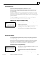
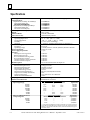
Specifications . . . . . . . . . . . . . . . . . . . . . . . . . . . . . . . . . . . . . . . . . . . . . . . . . . . .
4-2
Block Operation . . . . . . . . . . . . . . . . . . . . . . . . . . . . . . . . . . . . . . . . . . . . . . . . . .
4-3
Diagnostics . . . . . . . . . . . . . . . . . . . . . . . . . . . . . . . . . . . . . . . . . . . . . . . . . . . . . .
4-5
Field Wiring . . . . . . . . . . . . . . . . . . . . . . . . . . . . . . . . . . . . . . . . . . . . . . . . . . . . . .
4-8
Block Configuration . . . . . . . . . . . . . . . . . . . . . . . . . . . . . . . . . . . . . . . . . . . . . . .
4-10
115 VAC/125 VDC Isolated I/O Blocks . . . . . . . . . . . . . . . . . . . . . . . . .
GEK–90486D–2
1-1
5-1
Features . . . . . . . . . . . . . . . . . . . . . . . . . . . . . . . . . . . . . . . . . . . . . . . . . . . . . . . . .
5-1
Specifications . . . . . . . . . . . . . . . . . . . . . . . . . . . . . . . . . . . . . . . . . . . . . . . . . . . .
5-2
Compatibility . . . . . . . . . . . . . . . . . . . . . . . . . . . . . . . . . . . . . . . . . . . . . . . . . . . .
5-3
Block Operation . . . . . . . . . . . . . . . . . . . . . . . . . . . . . . . . . . . . . . . . . . . . . . . . . .
5-4
Diagnostics . . . . . . . . . . . . . . . . . . . . . . . . . . . . . . . . . . . . . . . . . . . . . . . . . . . . . .
5-6
Field Wiring . . . . . . . . . . . . . . . . . . . . . . . . . . . . . . . . . . . . . . . . . . . . . . . . . . . . . .
5-10
Block Configuration . . . . . . . . . . . . . . . . . . . . . . . . . . . . . . . . . . . . . . . . . . . . . . .
5-12
Genius I/O Discrete and Analog Blocks User’s Manual – September 1993
ix
Contents
Chapter 6
Chapter 7
Chapter 8
Chapter 9
115 VAC 16 Circuit Input Block . . . . . . . . . . . . . . . . . . . . . . . . . . . . . . .
Features . . . . . . . . . . . . . . . . . . . . . . . . . . . . . . . . . . . . . . . . . . . . . . . . . . . . . . . . .
6-1
Compatibility . . . . . . . . . . . . . . . . . . . . . . . . . . . . . . . . . . . . . . . . . . . . . . . . . . . .
6-1
Specifications . . . . . . . . . . . . . . . . . . . . . . . . . . . . . . . . . . . . . . . . . . . . . . . . . . . .
6-2
Block Operation . . . . . . . . . . . . . . . . . . . . . . . . . . . . . . . . . . . . . . . . . . . . . . . . . .
6-3
Optional Diagnostics . . . . . . . . . . . . . . . . . . . . . . . . . . . . . . . . . . . . . . . . . . . . .
6-4
Selecting Thresholds and Resistor Values . . . . . . . . . . . . . . . . . . . . . . . . . . . . .
6-6
Field Wiring . . . . . . . . . . . . . . . . . . . . . . . . . . . . . . . . . . . . . . . . . . . . . . . . . . . . . .
6-9
Block Configuration . . . . . . . . . . . . . . . . . . . . . . . . . . . . . . . . . . . . . . . . . . . . . . .
6-11
Relay Output Blocks . . . . . . . . . . . . . . . . . . . . . . . . . . . . . . . . . . . . . . . .
7-1
Features . . . . . . . . . . . . . . . . . . . . . . . . . . . . . . . . . . . . . . . . . . . . . . . . . . . . . . . . .
7-1
Compatibility . . . . . . . . . . . . . . . . . . . . . . . . . . . . . . . . . . . . . . . . . . . . . . . . . . . .
7-1
Specifications . . . . . . . . . . . . . . . . . . . . . . . . . . . . . . . . . . . . . . . . . . . . . . . . . . . .
7-2
Block Operation . . . . . . . . . . . . . . . . . . . . . . . . . . . . . . . . . . . . . . . . . . . . . . . . . .
7-3
Diagnostics . . . . . . . . . . . . . . . . . . . . . . . . . . . . . . . . . . . . . . . . . . . . . . . . . . . . . .
7-4
Field Wiring . . . . . . . . . . . . . . . . . . . . . . . . . . . . . . . . . . . . . . . . . . . . . . . . . . . . . .
7-5
Block Configuration . . . . . . . . . . . . . . . . . . . . . . . . . . . . . . . . . . . . . . . . . . . . . . .
7-7
16 Circuit DC Input/Output Blocks . . . . . . . . . . . . . . . . . . . . . . . . . . . .
8-1
Features . . . . . . . . . . . . . . . . . . . . . . . . . . . . . . . . . . . . . . . . . . . . . . . . . . . . . . . . .
8-1
Compatibility . . . . . . . . . . . . . . . . . . . . . . . . . . . . . . . . . . . . . . . . . . . . . . . . . . . .
8-1
Specifications . . . . . . . . . . . . . . . . . . . . . . . . . . . . . . . . . . . . . . . . . . . . . . . . . . . .
8-2
Block Operation . . . . . . . . . . . . . . . . . . . . . . . . . . . . . . . . . . . . . . . . . . . . . . . . . .
8-3
Diagnostics . . . . . . . . . . . . . . . . . . . . . . . . . . . . . . . . . . . . . . . . . . . . . . . . . . . . . .
8-5
Field Wiring . . . . . . . . . . . . . . . . . . . . . . . . . . . . . . . . . . . . . . . . . . . . . . . . . . . . . .
8-8
Block Configuration . . . . . . . . . . . . . . . . . . . . . . . . . . . . . . . . . . . . . . . . . . . . . . .
8-10
32 Circuit DC Input/Output Blocks . . . . . . . . . . . . . . . . . . . . . . . . . . . .
GEK–90486D–2
6-1
9-1
Features . . . . . . . . . . . . . . . . . . . . . . . . . . . . . . . . . . . . . . . . . . . . . . . . . . . . . . . . .
9-1
Compatibility . . . . . . . . . . . . . . . . . . . . . . . . . . . . . . . . . . . . . . . . . . . . . . . . . . . .
9-1
Specifications . . . . . . . . . . . . . . . . . . . . . . . . . . . . . . . . . . . . . . . . . . . . . . . . . . . .
9-2
Block Operation . . . . . . . . . . . . . . . . . . . . . . . . . . . . . . . . . . . . . . . . . . . . . . . . . .
9-3
Diagnostics . . . . . . . . . . . . . . . . . . . . . . . . . . . . . . . . . . . . . . . . . . . . . . . . . . . . . .
9-5
Field Wiring . . . . . . . . . . . . . . . . . . . . . . . . . . . . . . . . . . . . . . . . . . . . . . . . . . . . . .
9-6
Block Configuration . . . . . . . . . . . . . . . . . . . . . . . . . . . . . . . . . . . . . . . . . . . . . . .
9-8
Genius I/O Discrete and Analog Blocks User’s Manual – September 1993
x
Contents
Chapter 10 Voltage/Current Analog Input/Output Blocks . . . . . . . . . . . . . . . . . .
Features . . . . . . . . . . . . . . . . . . . . . . . . . . . . . . . . . . . . . . . . . . . . . . . . . . . . . . . . .
Compatibility . . . . . . . . . . . . . . . . . . . . . . . . . . . . . . . . . . . . . . . . . . . . . . . . . . . .
Specifications . . . . . . . . . . . . . . . . . . . . . . . . . . . . . . . . . . . . . . . . . . . . . . . . . . . .
Block Operation . . . . . . . . . . . . . . . . . . . . . . . . . . . . . . . . . . . . . . . . . . . . . . . . . .
Circuit Scaling . . . . . . . . . . . . . . . . . . . . . . . . . . . . . . . . . . . . . . . . . . . . . . . . . . . .
Diagnostics . . . . . . . . . . . . . . . . . . . . . . . . . . . . . . . . . . . . . . . . . . . . . . . . . . . . . .
Field Wiring . . . . . . . . . . . . . . . . . . . . . . . . . . . . . . . . . . . . . . . . . . . . . . . . . . . . . .
Block Configuration . . . . . . . . . . . . . . . . . . . . . . . . . . . . . . . . . . . . . . . . . . . . . . .
Chapter 11 Current-source Analog Input/Output Blocks . . . . . . . . . . . . . . . . . . .
Features . . . . . . . . . . . . . . . . . . . . . . . . . . . . . . . . . . . . . . . . . . . . . . . . . . . . . . . . .
Compatibility . . . . . . . . . . . . . . . . . . . . . . . . . . . . . . . . . . . . . . . . . . . . . . . . . . . .
Specifications . . . . . . . . . . . . . . . . . . . . . . . . . . . . . . . . . . . . . . . . . . . . . . . . . . . .
Block Operation . . . . . . . . . . . . . . . . . . . . . . . . . . . . . . . . . . . . . . . . . . . . . . . . . .
Diagnostics . . . . . . . . . . . . . . . . . . . . . . . . . . . . . . . . . . . . . . . . . . . . . . . . . . . . . .
Field Wiring . . . . . . . . . . . . . . . . . . . . . . . . . . . . . . . . . . . . . . . . . . . . . . . . . . . . . .
Block Configuration . . . . . . . . . . . . . . . . . . . . . . . . . . . . . . . . . . . . . . . . . . . . . . .
Chapter 12 Current–sour ce Analog 6 Output Blocks . . . . . . . . . . . . . . . . . . . . . .
Features . . . . . . . . . . . . . . . . . . . . . . . . . . . . . . . . . . . . . . . . . . . . . . . . . . . . . . . . .
Compatibility . . . . . . . . . . . . . . . . . . . . . . . . . . . . . . . . . . . . . . . . . . . . . . . . . . . .
Specifications . . . . . . . . . . . . . . . . . . . . . . . . . . . . . . . . . . . . . . . . . . . . . . . . . . . .
Block Operation . . . . . . . . . . . . . . . . . . . . . . . . . . . . . . . . . . . . . . . . . . . . . . . . . .
Diagnostics . . . . . . . . . . . . . . . . . . . . . . . . . . . . . . . . . . . . . . . . . . . . . . . . . . . . . .
Field Wiring . . . . . . . . . . . . . . . . . . . . . . . . . . . . . . . . . . . . . . . . . . . . . . . . . . . . . .
Block Configuration . . . . . . . . . . . . . . . . . . . . . . . . . . . . . . . . . . . . . . . . . . . . . . .
Chapter 13 Current-source Analog 6 Input Blocks . . . . . . . . . . . . . . . . . . . . . . . . .
Features . . . . . . . . . . . . . . . . . . . . . . . . . . . . . . . . . . . . . . . . . . . . . . . . . . . . . . . . .
Compatibility . . . . . . . . . . . . . . . . . . . . . . . . . . . . . . . . . . . . . . . . . . . . . . . . . . . .
Specifications . . . . . . . . . . . . . . . . . . . . . . . . . . . . . . . . . . . . . . . . . . . . . . . . . . . .
Block Operation . . . . . . . . . . . . . . . . . . . . . . . . . . . . . . . . . . . . . . . . . . . . . . . . . .
Diagnostics . . . . . . . . . . . . . . . . . . . . . . . . . . . . . . . . . . . . . . . . . . . . . . . . . . . . . .
Field Wiring . . . . . . . . . . . . . . . . . . . . . . . . . . . . . . . . . . . . . . . . . . . . . . . . . . . . . .
Block Configuration . . . . . . . . . . . . . . . . . . . . . . . . . . . . . . . . . . . . . . . . . . . . . . .
Chapter 14 RTD 6 Input Blocks . . . . . . . . . . . . . . . . . . . . . . . . . . . . . . . . . . . . . . . . .
Features . . . . . . . . . . . . . . . . . . . . . . . . . . . . . . . . . . . . . . . . . . . . . . . . . . . . . . . . .
Compatibility . . . . . . . . . . . . . . . . . . . . . . . . . . . . . . . . . . . . . . . . . . . . . . . . . . . .
Specifications . . . . . . . . . . . . . . . . . . . . . . . . . . . . . . . . . . . . . . . . . . . . . . . . . . . .
Block Operation . . . . . . . . . . . . . . . . . . . . . . . . . . . . . . . . . . . . . . . . . . . . . . . . . .
Diagnostics . . . . . . . . . . . . . . . . . . . . . . . . . . . . . . . . . . . . . . . . . . . . . . . . . . . . . .
Field Wiring . . . . . . . . . . . . . . . . . . . . . . . . . . . . . . . . . . . . . . . . . . . . . . . . . . . . . .
Block Configuration . . . . . . . . . . . . . . . . . . . . . . . . . . . . . . . . . . . . . . . . . . . . . . .
GEK–90486D–2
Genius I/O Discrete and Analog Blocks User’s Manual – September 1993
xi
10-1
10-1
10-1
10-2
10-3
10-5
10-6
10-7
10-8
11-1
11-1
11-1
11-2
11-3
11-6
11-7
11-8
12-1
12-1
12-1
12-2
12-3
12-5
12-6
12-7
13-1
13-1
13-1
13-2
13-3
13-4
13-5
13-6
14-1
14-1
14-1
14-2
14-3
14-5
14-6
14-7
Contents
Chapter 15 Thermocouple 6 Input Blocks . . . . . . . . . . . . . . . . . . . . . . . . . . . . . . . .
15-1
Features . . . . . . . . . . . . . . . . . . . . . . . . . . . . . . . . . . . . . . . . . . . . . . . . . . . . . . . . .
15-1
Compatibility . . . . . . . . . . . . . . . . . . . . . . . . . . . . . . . . . . . . . . . . . . . . . . . . . . . .
15-1
Specifications . . . . . . . . . . . . . . . . . . . . . . . . . . . . . . . . . . . . . . . . . . . . . . . . . . . .
15-2
Block Operation . . . . . . . . . . . . . . . . . . . . . . . . . . . . . . . . . . . . . . . . . . . . . . . . . .
15-3
Block Measurement Accuracy . . . . . . . . . . . . . . . . . . . . . . . . . . . . . . . . . . . . . .
15-4
Diagnostics . . . . . . . . . . . . . . . . . . . . . . . . . . . . . . . . . . . . . . . . . . . . . . . . . . . . . .
15-6
Field Wiring . . . . . . . . . . . . . . . . . . . . . . . . . . . . . . . . . . . . . . . . . . . . . . . . . . . . . .
15-7
Block Configuration . . . . . . . . . . . . . . . . . . . . . . . . . . . . . . . . . . . . . . . . . . . . . . .
15-8
Chapter 16 Sizing Enclosures . . . . . . . . . . . . . . . . . . . . . . . . . . . . . . . . . . . . . . . . . . .
16-1
Space Needed for Blocks . . . . . . . . . . . . . . . . . . . . . . . . . . . . . . . . . . . . . . . . . . .
16-1
Dimensions of Genius I/O Blocks . . . . . . . . . . . . . . . . . . . . . . . . . . . . . . . . . . .
16-2
Heat Dissipation . . . . . . . . . . . . . . . . . . . . . . . . . . . . . . . . . . . . . . . . . . . . . . . . . .
16-3
Chapter 17 I/O Point Redundancy . . . . . . . . . . . . . . . . . . . . . . . . . . . . . . . . . . . . . . .
17-1
Chapter 18 I/O Block Troubleshooting . . . . . . . . . . . . . . . . . . . . . . . . . . . . . . . . . . .
18-1
Block LEDs . . . . . . . . . . . . . . . . . . . . . . . . . . . . . . . . . . . . . . . . . . . . . . . . . . . . . .
18-1
Problems and Corrective Actions . . . . . . . . . . . . . . . . . . . . . . . . . . . . . . . . . . . .
18-2
Appendix A Ordering Information . . . . . . . . . . . . . . . . . . . . . . . . . . . . . . . . . . . . . . .
A-1
Appendix B Genius Blocks I/O Reference Usage . . . . . . . . . . . . . . . . . . . . . . . . . . .
B-1
Appendix C Non-Incendive Field Wiring . . . . . . . . . . . . . . . . . . . . . . . . . . . . . . . . . .
C-1
GEK–90486D–2
Genius I/O Discrete and Analog Blocks User’s Manual – September 1993
xii
restart lowapp ARestart oddapp: ARestarts for autonumbers that do not restart in
each chapter.
figure bi level
1, reset
table_big
level 1, reset chap_big level 1, reset1
Restarts
for autonumbers
that do
not restart
in each
chapter.
Lowapp Alwbox restart evenap:A1app_big level 1, resetA figure_ap
these restarts
level 1, must
reset be in the header frame of chapter 1.
figure
bi level
1, reset
a:ebx,restarts
l 1 resetA
table_ap
level
1, reset figure level 1, reset table level 1, reset these
table_big
1, 1evenbox
reset
1, 1.
resetA
oddboxlevel
reset:
reset: 1must be in the header frame ofa:obx:l
chapter
a:ebx, l 1
chap_big
1, 1,
reset1
a:bigbx
1 resetA
resetA level
a:obx:l
resetA a:bigbx level 1 resetA a:ftr level 1 resetA
c:ebx, level
l 1 reset1
app_big
1, resetA
a:ftr level
c:obx:llevel
1, reset1
c:bigbx level 1 reset1 c:ftr level 1 reset1 Reminders
for 1 resetA
figure_ap level 1, reset
c:ebx, l 1 reset1
autonumbers
that need to be restarted manually (first instancec:obx:l
will always
be 4)
table_ap
level 1, reset
1, reset1
let_in
level
1: A. B. C. letter level 1:A.B.C. num level 1: 1. 2. 3. num_in
1. 2.
figure
level
1, reset
c:bigbx level
level 1:
1 reset1
3.
rom_in
level
1:
I.
II.
III.
roman
level
1:
I.
II.
III.
steps
level
1:
1.
2.
3.
table level 1, reset
c:ftr level 1 reset1
Chapter
Reminders for autonumbers that need to be restarted
manually (first instance will always be 4)
let_in level 1: A. B. C.
letter level 1:A.B.C.
num level 1: 1. 2. 3.
num_in level 1: 1. 2. 3.
rom_in level 1: I. II. III.
roman level 1: I. II. III.
steps level 1: 1. 2. 3.
1 Introduction
1
This chapter contains the following basic information about Geniust I/O blocks:
H
H
H
H
H
Block description
Types of blocks available
Locations for Genius I/O blocks, and environmental specifications
Description of basic block operation
Features and benefits
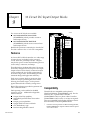
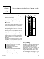
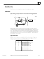
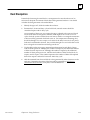
Block Description
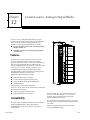
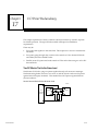
Genius I/O blocks are intelligent, self-contained, configurable I/O modules.
Ï
Ï
ÏÏ
ÏÏ
ÏÏ
ÏÏ
ÏÏ
ÏÏ
ÏÏ
ÏÏ
ÏÏ
ÏÏ
ÏÏ
ÏÏ
ÏÏ
ÏÏ
ÏÏ
ÏÏ
a44485
GENIUS
24/48 VDC
Source In/Out
GE Fanuc
2A/Pt Max 15A Max Total
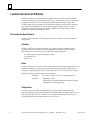
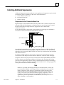
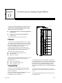
A Genius I/O block is made of cast aluminum, and weighs about 4 pounds (1.8 Kg).
Block size is approximately 9” (22 cm) x 4” (10 cm) x 3” (9 cm).
GEK-90486D-2
1-1
1
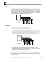
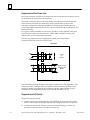
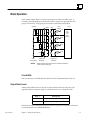
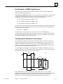
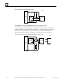
Parts of an I/O Block
A block consists of a matching Terminal Assembly and Electronics Assembly.. The
Terminal Assembly forms the base of the block. It is electrically and mechanically keyed
to accept only an Electronics Assembly of the same type (voltage, number of circuits,
wiring configuration). All field wiring connections are made to the Terminal Assembly.
All active components, I/O and communications circuits are located in the Electronics
Assembly. The Electronics Assembly can be removed without disturbing field wiring.
The block’s configuration is stored in the Terminal Assembly, so there is no need to
reconfigure the block if the Electronics Assembly is changed.
Electronics
Assembly
Retaining
Screws
Terminal
Assembly
Ï
ÏÏ
Ï
ÏÏ
ÏÏ
Ï
ÏÏ
1-2
Genius I/O Discrete and Analog Blocks User’s Manual – September 1993
GEK-90486D-2
1
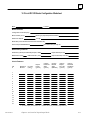
Types of Genius I/O Blocks
Many types of Genius I/O blocks are available, to interface a wide range of field devices
to a Genius communications bus.
Discrete Blocks
115 VAC Grouped I/O Block
I/O Circuits
For information, see:
8,I/Oconfigurable
chapter 4
8,I/Oconfigurable
chapter 5
115 VAC 16–circuit Input Block
16 inputs
chapter 6
115VAC/230V
AC Relay Output Block, Normally–Closed outputs
16 relay
chapter 7
16,I/Oconfigurable
chapter 8
32,I/Oconfigurable
chapter 9
4 inputs, 2 outputs
chapter 10
4 inputs, 2 outputs
chapter 11
115 VAC Grouped I/O Block, Low–leakage
115VAC/125VDCIsolatedI/OBlockwithoutput
Failed Switch diagnostic
115VAC/125VDCIsolatedI/OBlock,nooutput
Failed Switch diagnostic
115VAC/230V
AC Relay Output Block, Normally–Open
24 VDC Source I/O Block, 16 Circuit
24/48 VDC Source I/O Block, 16 Circuit
24 VDC Sink I/O Block, 16 Circuit
24/48 VDC Sink I/O Block, 16 Circuit
12/24 VDC Source I/O Block, 32 Circuit
5/12/24VDCSinkI/OBlock,32Circuit
115 VAC/125VDCAnalogI/OBlock
24/48VDCAnalogI/OBlock
115 VAC/125VDCCurrent–source Analog I/O
Block
24/48VDCCurrent–source Analog I/O Block
115VAC/125VDCCurrent–source Output Block 6 outputs
chapter 12
24/48VDCCurrent–source Output Block
115VAC/125VDCCurrent–source Input Block
6 inputs
chapter 13
6 RTD inputs
chapter 14
6 t’couple inputs
chapter 15
High–speed Counter
Configurablecounterinputs/modes
High–speed Counter User’s
Manual GFK–0415
PowerTRAC Block
Inputs from 1–3 PTs, PowerTRAC Block User’s
1–3 CTs
Manual GFK–0450
24/48VDCCurrent–source Input Block
115 VAC/125VDCRTD Input Block
24/48VDCRTD Input Block
115 VAC/125VDCThermocouple Input Block
24/48VDCThermocouple Input Block
GEK-90486D-2
Chapter 1 Introduction
1-3
1
Locations for Genius I/O Blocks
Unlike conventional rack–mounted I/O modules, Genius I/O blocks can be installed
virtually anywhere, up to 7500 feet from the PLC or computer. They can be mounted on
equipment, in junction boxes, inside panels, behind operator stations, and in other
locations where space is limited. Blocks should be located in an area which is clean and
free of airborne contaminants. There should be adequate cooling airflow. In many
applications, Genius I/O blocks are installed in NEMA enclosures. Chapter 15 gives
guidelines for determining enclosure sizes.
Environmental Specifications
Genius I/O blocks meet the following specifications for vibration, noise. and ambient
temperature.
Vibration
Genius I/O blocks are compact and sturdy; they perform well in conditions where
vibration is a factor. All Genius I/O block designs are vibration–tested (according to
Mil–Std 810C and IEC 68–2–6) to meet the following specifications:
5 to 10 Hz .200 in displacement (peak to peak)
10 to 200 Hz at 1 g
Shock: 15G
Noise
Genius I/O blocks are resistant to noise levels found in most industrial applications when
installed according to accepted industry practices. This includes proper separation of
wiring by voltage and power levels, as explained in the Genius I/O System User’s Manual.
Blocks are tested to the following noise specifications:
Radiated:
FCC part 15, section J, class A, Computing Devices
Received:
NEMA ICS 2–230
ANSI/IEEE C37.90 (Relay and relay systems associated
with Electrical Power Apparatus)
Temperature
I/O blocks operate reliably in temperatures up to 60C (140F). Temperatures are
measured adjacent to the block at the bottom of the Electronics Assembly. Between 35C
and 65C (95–149F) each 10C reduction in the ambient temperature increases the
electronics Mean Time Between Failures by a factor of two.
1-4
Genius I/O Discrete and Analog Blocks User’s Manual – September 1993
GEK-90486D-2
1
Block Operation
A Genius I/O block is an intelligent module that sends and receives messages on a
communications bus.
The devices on the bus pass an implicit token, which rotates among the devices in
sequence from device 0 to device 31. This sequence is called a bus scan.
Bus
Controller
(Device 31)
Token Path
1
2
3
30
A block can send:
Input data (if the block has inputs).
Diagnostic fault reports.
A block can receive:
Output data from the CPU.
Commands from the CPU and Hand–held Monitor.
Inputs
A block (with inputs) continuously monitors data from its input devices and updates the
corresponding data. When the block receives the bus token, it broadcasts ALL its current
input data. The bus controller stores this data, making it available to the CPU. Even
blocks with no inputs put out a message when they get the token, to notify the bus
controller that they are present and on–line.
Bus
Controller
Inputs from Block 4
1
= token
GEK-90486D-2
Chapter 1 Introduction
2
3
4
1-5
1
Outputs
As the application program executes, the CPU sends outputs and any commands to the
bus controller. The bus controller stores this data until it receives the bus token. Then, it
directs output data to each of the blocks on the bus, and commands to the appropriate
devices. Even blocks that have no outputs receive a null message from the bus controller
while it has the token. This permits the blocks to indicate that they are on–line with the
CPU, and to detect loss of communications should that occur.
Outputs
Bus
Controller
D
1
2
3
4
D = token
Diagnostics
If a block detects a fault, the following things happen:
1.
The block’s Unit OK LED blinks to show that a fault exists.
2.
Unless the fault reporting feature has been disabled for the circuit where the fault
occurred, the block automatically sends a fault message to the bus controller and/or
monitoring CPU on the next available bus scan. This fault information is always
available to the Hand–held Monitor, which continually polls the block for updates.
Bus
Controller
Inputs and Fault Message
from Block 3
1
D = token
2
3
4
F
F
D
F = fault
3.
For certain types of faults, the block takes corrective action in order to prevent
possible hazardous operation, or damage to the block. For example, for some output
faults, the block automatically turns the output off.
Faults may be cleared from the Hand–held Monitor or the CPU. If the condition that
caused the fault has not been corrected, the block sends another fault message after the
fault is cleared. If the block has shut down a circuit in response to a fault condition and
the condition has been corrected, the block restores that circuit to full operation as soon
as the fault is cleared.
1-6
Genius I/O Discrete and Analog Blocks User’s Manual – September 1993
GEK-90486D-2
1
Features and Benefits of Genius I/O
The potential benefits to be derived from using Genius I/O products include:
H
H
H
H
Reduced software engineering
Faster startup
Installation cost savings
Reduction in costly downtime
Genius I/O provides these cost savings through:
Configuration Flexibility: Many discrete Genius I/O blocks have programmable I/O
circuits, allowing any mix of inputs and outputs. That means a single 8–circuit block
would be field–configurable to any of 256 distinct combinations of inputs and outputs.
Intelligence: With a Genius I/O system, you can program many conventionally
hard–wired features of I/O systems. With Genius I/O, filter time constants, default
values, and other characteristics can be field–configured and customized for the
attached devices. Analog blocks have built–in engineering unit scaling. The cost and
productivity benefits are reduction in initial custom engineering and improved use of
equipment.
Reduced installation costs: for wiring, terminal blocks, conduit, and junction boxes.
Because Genius I/O blocks are mounted at the point of control, the distribution panels,
ducts, and auxiliary power supplies associated with most remote I/O systems are largely
avoided. Reduced installation cost comes from the simpler wiring and reduction in
custom panels and ducting – saving both materials and labor. Before programming
begins, the entire I/O system can be tested and possible malfunctions can be prevented.
Blocks can be removed and inserted without disturbing field wiring, which is connected
to the separate Terminal Assembly.
Advanced Diagnostics: In addition to being able to detect internal faults, a Genius I/O
system can detect open circuits, short circuits, overloads, and a variety of other faults in
the attached devices. Many faults can be detected before they cause a malfunction in
equipment. The system can detect the integrity of a control circuit before the circuit must
actually be energized. This is made possible by periodic “pulse–testing” under
microprocessor control within a Genius I/O block. The system can specifically isolate and
identify faults to the circuit level for prompt and accurate maintenance.
Circuit Protection: Many Genius I/O blocks provide electronic fusing and overload
protection. Blocks can shut circuits down within 5 microseconds of detecting circuit
faults, providing far more effective protection than thermal fuses. Short circuits and
overloads may be reset from the programmable controller or Hand–held Monitor.
Productivity benefits include reduced maintenance time and better protection of
equipment.
GEK-90486D-2
Chapter 1 Introduction
1-7
1
Beyond these benefits, the flexibility, power, and intelligence built into the Genius I/O
system can make production and equipment–design engineering easier; Genius I/O
systems will monitor, control and diagnose the next generation of devices in tomorrow’s
factories.
1-8
H
High–level analog signals on can be mixed on one block: ( " 10 volts DC, " 5 volts
DC, 0–10 volts DC, 0–5 volts DC, 1–5 volts DC, or 4–20 mA).
H
Linear conversions can be established for analog blocks, converting analog values to
engineering units.
H
High–level and low–level alarms on analog inputs will automatically warn of
undesired analog levels.
H
Over–range and under–range diagnostics automatically report analog values that
are out of range.
H
The Hand–held Monitor can force I/O on and off and perform wiring diagnostics
with or without the CPU connected. A system can be wired and debugged in stages
without a program ever having been written.
H
H
Diagnostics will detect I/O block additions and deletions at remote locations.
H
Redundancy features can be used to provide protection from cable breaks, interface
module failure, or CPU failure. Redundancy features also permit the use of multiple
CPUs for distributed control or data monitoring.
Selectable Input Filter Times permit customizing input response to ambient electrical
environment. Longer filter times can be used to reject electrical noise in harsh
environments.
Genius I/O Discrete and Analog Blocks User’s Manual – September 1993
GEK-90486D-2
Chapter
2 Installation
2
section level 1 1
figure bi level 1
table_big level 1
This chapter includes installation instructions for:
H
H
H
H
H
H
H
Mounting I/O blocks
Making bus connections
Grounding I/O blocks
Installing additional suppression for certain types of output loads.
Interfacing small loads to some discrete AC blocks
Adding or removing a block’s Electronics Assembly
Replacing a block or Terminal Assembly
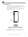
Mounting I/O Blocks
Genius I/O blocks can be mounted in any position. For adequate heat dissipation,
vertical mounting is recommended. If alternate blocks are mounted upside down,
bundles of wiring can be run between blocks.
ÎÎ
ÎÎ
ÎÎ
ÎÎ
ÎÎ
ÎÎ
ÎÎ
ÎÎ
a42836
ÎÎ
ÎÎ
Leave at least 1-1/2 inch (3.84 cm) of space between blocks, and 3 inches (7.62 cm) above
and below each block. This allows room for future use of a Block Puller to remove the
block’s Electronics Assembly. It also provides space for wiring (more space is desirable,
especially if wiring will be bundled together). If blocks will be located close together, it
may be easier to complete wiring before mounting the blocks. This is particularly true for
analog blocks and 32–Circuit DC blocks; wiring for those blocks enters the terminal strip
from the side.
GEK–90486D–2
2-1
2
If blocks are mounted in an enclosure,
there must be space for free flow of air
along each block’s Electronics Assembly
(the side opposite the Terminal
Assembly). Do not allow wiring
conduits, shelves, or other components
(including projections on the cover or
door) to inhibit cooling airflow around
the blocks. If an enclosure must be
located in direct sunlight, consider
placing a shade over it and/or painting
it white to reflect heat.
Tapped:
.136in (3.45mm)
(#29 drill)
Through hole:
.177in (4.5mm)
(#16 drill or larger)
Mounting Footprint
For each block, drill two screw or bolt
holes for 8–32 hardware. Notice that
the mounting holes are not centered.
Position the block so that the notches in
the upper and lower flanges line up
with the mounting holes. Attach the
block using 8–32 hardware.
8.45in (21.46cm)
8.75in (22.22cm)
3.25in
(8.26cm)
1.32in
(3.35cm)
2-2
Genius I/O Discrete and Analog Blocks User’s Manual – September 1993
0.150in (0.38cm)
GEK-90486D-2
2
Making Bus Connections
Make the bus connections to I/O blocks using the cable type selected for the application.
Recommended cable types are listed in the Genius I/O System User’s Manual.
Caution
Do not mix cable types on a bus. Unreliable communications could
result.
Bus connections can be made using either a slotted screwdriver (0.25” x 0.04” or 6.35mm
x 1.0mm maximum blade size) or a Phillips screwdriver (size 0 or 1). The tie–down
screws can be removed to accommodate ring–type connectors.
Note
On new block, the tie–down screws are tightened. If a block is to be
moved after the tie–down screws have been loosened, they should be
re–tightened to prevent loose screws from falling into the packaging
material or equipment.
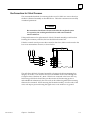
The bus cable connects to the Serial 1, Serial 2, Shield In and Shield Out terminals
(terminals 1–4). Connect the Serial 1 terminal of each block to the Serial 1 terminals of
the previous device and the next device. Connect the Serial 2 terminal of each block to
the Serial 2 terminals of the previous device and the next device.
Shield In of each block must be connected to Shield Out of the preceding device. For the
first device on the bus, Shield In can be left unconnected. For the last device on the bus,
Shield Out can be left unconnected.
End
of Bus
Start
of Bus
Terminating
Resistor
Terminating
Resistor
Serial 1
Serial 2
Shield In
Shield Out
Serial 1
Serial 2
Shield In
Shield Out
Note
Do not strip more insulation than necessary from the cable wires. The
maximum exposed length of bare wires should be two inches. For
added protection, each shield drain wire should be insulated with
spaghetti tubing to prevent the Shield In and Shield Out wires from
touching each other.
GEK-90486D-2
Chapter 2 Installation
2-3
2
Prefabricated Cables
For applications using Belden 9182 cable only, prefabricated cables in 15” (IC660BLC001)
and 36” (IC660BLC003) lengths are available. These cables terminate in mating
connectors that simplify wiring between I/O blocks.
SER 2
SER 1
SHD IN
SHD OUT
SHD SHD SER SER
OUT IN
2
1
Terminating the Bus at an I/O Block
For devices on either end of the bus, install the appropriate terminating resistor across
the Serial 1 and Serial 2 terminals. Impedance will be 75, 100, 120, or 150 ohms. 150 ohm
(IC660BLM506) and 75 ohm (IC660BLM508) resistor plugs can be ordered.
If blocks are connected using the prefabricated cables described above, attach the cable
to the first or the last block to exit toward the top of the block. A 150 ohm terminating
plug should then be installed across Serial 1 and Serial 2.
'
S1
S2
SHLD IN
SHLD OUT
2-4
Genius I/O Discrete and Analog Blocks User’s Manual – September 1993
GEK-90486D-2
2
Bus Connections for Critical Processes
The recommended method of connecting the bus to an I/O block is to wire it directly to
the block’s Terminal Assembly as described above. These bus connections are normally
considered permanent.
Caution
Bus connections should never be removed while the completed system
is in operation; the resulting unreliable data could cause hazardous
control conditions.
If the possible removal or replacement of a block’s Terminal Assembly would result in
breaking the continuity of the bus, the bus should first be turned off.
If the bus controls critical processes that cannot be shut down, blocks can be wired to the
bus via an intermediate connector, as shown below.
I
N
O
U
T
S1
S2
SHLD IN
SHLD OUT
'
S1
S2
SHLD IN
SHLD OUT
This will allow the block’s Terminal Assembly to be removed while maintaining data
integrity on the bus. The connector shown is #A107204NL from Control Design, 458
Crompton Street, Charlotte NC, 28134. If blocks are connected to the bus in this way,
field wiring to the blocks should also provide a means of disconnecting power to
individualblocks.Alternatively, the wire ends can be soldered together before inserting
them into the terminals. When removing the Terminal Assembly, cover the ends of the
wires with tape to prevent shorting the signal wires to one another or to ground.
GEK-90486D-2
Chapter 2 Installation
2-5
2
Grounding I/O Blocks
The Shield Out termination of each block is connected directly to the block’s chassis
ground. The Shield Out termination is capacitively coupled to Shield In. This breaks up
any differences in small ground voltages which may be present at different blocks on the
bus (up to 50V of continuous difference of ground potential).
Within each cabinet, use hardware such as star washers to provide ground integrity. A
ground wire (minimum size AWG #12) must be connected from the ground screw on
each Genius I/O block to the panel.
Grounding
Screw
Alternate
Ground
Connection
Point
Warning
If the mounting screws do not make good ground connection and the
grounding screw is not connected to a reliable ground, the block is not
grounded, Electrical shock hazard exists. Death or personal injury
may result.
Normally a ground (green) ground conductor is routed from the building power system
to each control cabinet. Metal wire conduits should NOT be used as the only earth
ground connection.
2-6
Genius I/O Discrete and Analog Blocks User’s Manual – September 1993
GEK-90486D-2
2
Installing Additional Suppression
Additional suppression may be needed in some applications. Suppression may located in
the following places, depending on the source of the disturbance:
A. At the communications line.
B. Across the power line.
C. At the I/O points.
Suppression at the Communications Line
High transients on the communications bus may render some I/O blocks inactive and
turn their LEDs off. If that happens, cycling block power restores operation. To guard
blocks from the affects of high transients, suppression can be added at the
communications line.
For an individual block, suppression can be supplied by connecting two small MOVs
from Serial 1 and Serial 2 to the block’s Shield Out terminal:
(bus cable not shown)
S1
S2
MOVs
SHLD IN
SHLD OUT
Suitable MOVs include Harris part number V220MA2A, Panasonic ERZ–CO5FK221U,
and Siemens 505K140. If necessary, higher energy rated devices can also be used. It is
important to be sure that the MOV leads do not cause any shorts between the serial data
and shield connectors.
For blocks installed together in an enclosure, suppression can be added at the point
where the bus cable and power lines enter the enclosure, as shown on the next page.
Chapter 2 of the Genius I/O System and Communications Manual (GEK-90486-1) describes
the noise-rejection and filtering capabilities of the Genius bus. It explains bus wiring
practices for all applications. Chapter 2 also gives additional instructions for installing a
bus outdoors or between buildings, including recommendations for adding suppression
at the point where the bus enters a building.
Note
MOVs do a good job of absorbing transients on communications, control, and
power lines, provided the total energy of those transients does not exceed the
rating of the device. If the energy of the transient exceeds the rating of the
device, the MOV may be either damaged or destroyed. This failure may not be
visibly or electrically evident. MOVS should be regularly inspected for signs of
damage to assure continued protection against transients. For some
applications, periodic replacement of critical MOVs, even if they do not show
signs of damage, is recommended.
GEK-90486D-2
Chapter 2 Installation
2-7
2
Suppression at the Power Line
Power line transients can affect any Genius block that has separate power inputs, such as
AC Isolated blocks and low level analog blocks.
Protection can be provided by connecting MOVs across the power lines (for instance,
between Hot and Neutral) and from line to frame ground (safety ground). This
triangular configuration requires three MOVs for each long power feed. If the total
power feed length is about 100 feet or less, one set of MOVs should be sufficient for any
number of blocks.
For a group of blocks installed in an enclosure, the MOVs can be installed at the point
where the power lines enter the enclosure. Ideally, MOVs should be used at each
cabinet in the system for maximum protection.
The following illustration shows suppression on both power lines and the
communications bus for blocks in an enclosure.
Enclosure
Power
to
Blocks
Short Length
of Bus to All
Blocks
The axial-leaded LA series of MOVs from Harris is often used for this application. The
14mm size, model V130LA10 rated at 38 joules is usually sufficient. The MOVs used
should be capable of handling the line transients expected. Measurement of actual
transients may be required in extreme cases to decide what MOVs to use.
Suppression at I/O Points
Suppression may be needed:
A. At the inputs of some sensitive blocks, such as RTD blocks. Instructions for wiring
MOVs to RTD inputs are included with the RTD wiring information in chapter 14.
B. At a discrete output load, if there is excessive stored load energy, or if there is a
mechanical contact in series with a driven output coil.
2-8
Genius I/O Discrete and Analog Blocks User’s Manual – September 1993
GEK-90486D-2
2
Suppression at the Output Load
Most solid state controls include load suppression within the output drive. AC solid state
relays and proximity switches turn off at low currents with some internal suppression.
DC devices usually specify suppression if not included with the device. Additional
suppression is required if:
1.
The stored load energy to be dissipated exceeds the rating of the block’s output
suppressor during the turn–off discharge time.
2.
A mechanical contact is used in series with a driven output coil. Install additional
suppression such as a series resistor capacitor snubber to counteract electrical noise
that occurs when the coil is switched by the external contact instead of the block.
Resistor–capacitor suppressors are preferred for low-current high-inductance loads that
generate a high rate of change in voltage (dv/dt). High power loads beyond the capacity
of RCs use voltage clamping devices such as MOVs, which are usually available from the
manufacturer of the device. Resistor-capacitor suppressors are also preferred to MOVs or
transorbs because they reduce EMI in addition to absorbing load energy.
In general, the capacitor for an RC snubber should be the same value in microfarads as
the coil current in amperes, with the voltage rating at least twice the peak supply
voltage. The resistor is usually equal to the DC resistance of the coil. With DC coils, the
capacitor is usually replaced with a “flyback” diode oriented with the anode to the
negative terminal of the coil. The resistor helps maintain a fast dropout of the device; it
can be eliminated if this is not of concern.
Most control and contactor manufacturers make suppressor accessories that can be
conveniently mounted on their devices. The following types are available from GE
General Purpose Control, Bloomington, IL:
Type
Voltage
Part Number
RC
110 – 180 VAC
380 – 480 VAC
24 – 48 VAC
CR4XS1B
CR4XS1C
CR4ZS1J
Diode
12 – 250 VDC
CR4XS2P
Varistor
24 VDC
36 – 48 VDC
110 – 150 VDC
220 – 250 VDC
CR4XS3L
CR4XS3M
CR4XS3N
CR4XS3P
For NEMA size 0 – 6 contactors: CR305X146C
Consult other manufacturers for recommendations of equivalent suppressors for their
devices. Discrete components can also be used as discussed earlier. Pheonix Contact Inc.,
Weidmuller Inc., and other manufacturers make DIN rail mount suppressors for both
load snubbing and line surge protection.
If noise is generated by a protective contact that operates only in abnormal conditions,
not as part of the normal machine cycle, the best way to handle possible control
shutdown which may occur during machine faults depends on the application.
Normally, re–cycling block control power will enable resumption of operation.
GEK-90486D-2
Chapter 2 Installation
2-9
2
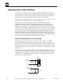
Interfacing Small Loads to AC Blocks
The 115 VAC Low–Leakage 8 Circuit Grouped I/O block (IC660BBD101) is designed to
interface small loads to the bus without added resistance at the load. For other types of
discrete AC blocks, if individual output circuits will drive inductive loads drawing less
than 50mA, it may be necessary to add resistance to the circuit at the load.
When closed, electromechanical devices such as contactors, starters, or relays have very
high inductance combined with a low value of holding current.
When the output is off, the inductance of the coil can interact with the block’s
suppression capacitor to maintain a relatively high current level (15mA to 25mA) over
the entire voltage range. That can make dropout operation (opening the contacts)
marginal, or cause the device to remain in the ON position. When the device releases,
the increased air gap reduces the coil inductance to a low value. That causes the current
leakage to decrease to the nominal 10mA to 13mA range, and the load voltage drops to a
very low value. Since the current required to pick up (energize) the device is usually
higher than the holding current, the leakage seldom causes a related device to pick up.
This interaction between leakage currents and load characteristics may falsely suggest
that a relay is stuck for mechanical rather than electrical reasons. If this happens, test the
device. If necessary, add additional load resistance across the load.
External Load Resistance for Coils and Lamps
If added resistance is needed, locate it at the load, not at the I/O block. The added
resistance should bring the total current up to 100mA. For example, for the General
Electric CR4CA contactor the holding current is specified as 9.1VA. This equates to about
79mA of load current. To increase the load current to 100 mA, a 4K ohm resistor would
be added in parallel across the relay coil. In case of doubt, use a lower resistance/higher
wattage value.
Resistive loads are less critical than inductive loads. The OFF state open circuit voltage
of the output circuit is approximately 80 volts. The voltage decreases linearly as lower
resistance loads are applied. For a 1000–ohm resistor load, the typical output OFF state
voltage is 14 volts. Incandescent lamps rated at less than 5 watts may glow dimly. To
prevent this, use parallel resistance.
Contactor/
Starter Coil
Genius
Output
External
Load
Resistor
115 N
Genius
Output
External
Load
Resistor
Lamp
115 N
2-10
Genius I/O Discrete and Analog Blocks User’s Manual – September 1993
GEK-90486D-2
2
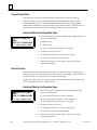
Adding or Removing a Block’s Electronics Assembly
All field wiring connections to a Genius I/O block are made to the block’s Terminal
Assembly, which is ordinarily permanently installed. This means the block’s Electronics
Assembly can be removed and replaced without disturbing field wiring, entering
addressing, or reconfiguring the block. The Terminal Assembly is mechanically keyed to
accept only an Electronics Assembly of the same type (voltage, number of circuits, wiring
configuration).
Removing an Electronics Assembly
A Block Puller (IC660BLM507) should always be used to remove or insert an Electronics
Assembly.
Caution
Use of a Block Puller prevents damage to the block connectors that can
result from manual removal. Such damage may result in unreliable
operation under high vibration conditions.
To remove an Electronics Assembly:
1.
Unscrew the retaining screws at the top and bottom of the block.
2.
Engage the tabs on the Block Puller in the first vent slots. Move the tool to the
center of the block and squeeze the handle.
Î
ÎÎ
Î
ÎÎ
Î
Î
ÎÎ
Î
Î
Î Î
a44606
ÎÎ
ÎÎ
ÎÎ
ÎÎ
ÎÎ
ÎÎ
3.
GEK-90486D-2
Î
Pull the Electronics Assembly straight away from the Terminal Assembly.
Chapter 2 Installation
2-11
2
An operating block may be hot to the touch. Test the surface of the block before
grasping it.
Warning
If power is applied to the field terminals, power is also exposed on the
connector pins at the base of the Terminal Assembly, and electrical
shock hazard exists. Do not touch the connector pins! Death or injury
may result.
Installing an Electronics Assembly
To replace an Electronics Assembly:
1.
Align the Electronics Assembly within the guides and push it down quickly.
Caution
Do not exert excessive force. Damage to the equipment might result.
If unusual resistance is met, remove the Electronics Assembly. If power is applied to
the block, DO NOT TOUCH THE CONNECTOR PINS! Inspect the Terminal
Assembly, connector receptacle, and connector edge board (on the Electronics
Assembly). Be sure the keying matches. Remove any obstacles and reinsert the
Electronics Assembly. Pay close attention to the alignment of the guide pins.
2.
Secure the Electronics Assembly with the screws on the top and bottom of the
Terminal Assembly.
Caution
If the retaining screws are loose, the connector pins may not make
contact correctly. This could result in faulty block operation.
Replacing a Block or Terminal Assembly
Do not add or remove a Genius I/O block or Terminal Assembly while the system is
operating unless the bus has been attached using a bus connector (see page 2-5), or the
bus wires have been soldered together.
Caution
Adding or removing an entire Genius I/O block or a Terminal
Assembly without taking these precautions may disrupt
communications. This may cause erratic operation or lead to system
shutdown.
2-12
Genius I/O Discrete and Analog Blocks User’s Manual – September 1993
GEK-90486D-2
2
If a removable connector has been used or the signal wires are soldered together, the
block’s Terminal Assembly can be replaced without powering down the bus.
If possible, do not remove the Terminal Assembly until a replacement is available. Then
replace the Terminal Assembly or block by following these steps carefully:
1.
If the block is still receiving power, remove power from the block. Take care to
ensure continued operation of any other devices wired to the same power supply.
Warning
Hazardous voltages may be present at the block’s field wiring
terminals while the block is receiving power. Death or injury may
result from contact with field wiring terminals.
2.
If a bus connector has been used, remove the bus connector from the Terminal
Assembly. Do not remove the bus wiring from the connector. The connector will maintain
continuity of data transfer on the bus.
I
N
O
U
T
S1
S2
SHLD IN
SHLD OUT
S1
a
S2
SHLD IN
SHLD OUT
Place the connector, with the bus still attached, in a protected location. Insulate the
connector ’s protruding pins.
Caution
If the connector pins come in contact with conductive material, data on
the bus may be corrupted, possibly causing the system to shut down.
If the signal wires have been joined by soldering instead of using a bus connector,
remove and tape each wire pair carefully. Do not allow the signal wires to contact
each other or any conductor.
3.
Remove the block’s Electronics Assembly.
4.
Remove field wiring from the Terminal Assembly.
5.
Remove and replace* the Terminal Assembly.
Reverse the procedure to install the new Terminal Assembly.
*
GEK-90486D-2
If removal of the block is permanent (no replacement is anticipated) the bus should be rewired
using unbroken cable at the earliest opportunity.
Chapter 2 Installation
2-13
Chapter
3 Configuration
3
section level 1 1
figure bi level 1
table_big level 1
This chapter explains:
H
H
H
H
H
H
What block configuration includes.
How to get started configuring I/O blocks.
How to set up a block for offline configuration.
The features of the configuration Main Menu.
How to assign a block’s required features.
How to assign additional block features.
Configuration Overview
Configuration is the process of selecting the features that will be used by a Genius I/O
block. Configuration includes:
1.
Assigning a Device Number to the block. This step, which requires a Hand–held
Monitor, must be done before any additional configuration can take place.
2.
For some CPU types, it is necessary to assign a Reference Address for the block’s I/O.
This also must be done with a Hand–held Monitor.
3.
Making sure the block’s configured baud rate matches that of other devices on the
bus.
4.
Selecting other features that are appropriate for the application. Block
configuration is simple, since all blocks come supplied with a set of default selections
for each feature. Therefore, configuration is only a matter of changing those
features that are appropriate for the application. Among the features of Genius I/O
blocks that can be configured are fault reporting, redundancy, and the assignment of
inputs and outputs on most discrete blocks. This configuration is usually done with
a Hand–held Monitor, but it can be done from the CPU.
5.
Protecting the block’s selected features so they will not be accidentally changed.
Many of a block’s configurable features can be changed at any time, even while the
system is in operation.
Blocks can be configured before or after installation on a properly–terminated serial
bus. If a new, factory–shipped block is to be added to an existing bus running at a baud
rate other than 153.6 Kbaud standard, the block must first be configured off–line. In
general, special care must be taken when adding new blocks to existing systems. Always
verify beforehand that the baud rate programmed for use by the new block corresponds
to that of the system – never mix baud rates on a single bus.
GEK-90486D-2
3-1
3
Preliminar y Steps
Block configuration should be carefully planned, and recorded on copies of the
configuration worksheets provided in this manual. Before block configuration starts,
you should already know:
H
H
What each block’s Device Number (address on the bus) should be.
H
H
The baud rate that will be used by the bus and all its devices.
The beginning Reference Address for each block’s I/O, if required for the type of
CPU controlling the bus.
Which of the block’s default features (for example, I/O mixture, Input Filter Time or
Alarm Thresholds) should be changed by configuration.
If you do not have the necessary information, do not try to configure any blocks.
Configuration Protection
All Genius I/O blocks can be configured for Configuration Protection, which prevents
unwanted or accidental changes. On a new block, Configuration Protection is disabled,
so the block is ready to configure for the application.
Removing Configuration Protection
On a previously–configured block, it may be necessary to disable Configuration
Protection to make changes. Configuration Protection can only be set and removed with
a Hand–held Monitor; it CANNOT be changed from the application program.
Use the HHM to step through the block configuration screens (the HHM does not have
to be connected directly to the block). The final screen that appears is the Configuration
Protection screen.
3-2
1.
Press F2 (Toggle) to select DISABLED.
2.
Press F3 (Enter) to save the selection.
3.
Press F4 (Next) to go to the first block configuration display, or ∆MENU to return to
the Configuration menu, or HOME to return to the Home menu.
Genius I/O Discrete and Analog Blocks User’s Manual – September 1993
GEK-90486D-2
3
Setting Up a Block for Off–line Configuration
It may be most convenient to configure new I/O blocks offline at a central location. Each
block will need to be connected to an appropriate source of power and to earth ground.
To prepare a block for off–line configuration:
1.
Connect a 75 ohm resistor across the Serial 1 and Serial 2 terminals, or use the 75
ohm terminator plug (IC660BLM508). Two of these plugs are provided with each
Bus Controller.
2.
Attach a grounding strap to the ground screw on the side of the block. Be sure that
the strap is connected to earth ground.
Warning
If the block is not properly grounded, hazardous voltages may exist.
Death or injury may result.
3.
Wire the block to the power source.
a42468
Attach
Ground
Strap
ÎÎ
Î
ÎÎ
Î
ÎÎ
Î
1
1
2
2
SHD IN
3
SER
SER
SHD OUT
Terminator
Plug
4
H
Î
To
Appropriate
AC or DC
Power
N
Warning
DO NOT TOUCH the connectors or wiring after powering up the
block. Hazardous voltages exist, and death or injury may result.
4.
GEK-90486D-2
Apply power to the block. Continue with the configuration instructions that follow.
Chapter 3 Configuration
3-3
3
Starting Configuration
Note
If you are configuring a block that is on an operating bus, the HHM
must be the ONLY Hand–held Monitor plugged into a block on the
bus.
1.
Begin with the Hand–held Monitor turned off. Attach the HHM to the block.
ÎÎ
Î
ÎÎ
Î
ÎÎ
Î
Î
ÎÎ
ÎÎ
Î
ÎÎ
Î
ÎÎÎÎ
Î
ÎÎÎ
ÎÎ Î
Î
Î
2.
3-4
a42307
Turn the Hand–held Monitor on. After the HHM completes its powerup sequence,
the Home menu appears. The Hand–held Monitor’s Change Block Configuration
option must be enabled to complete the instructions in this section. For a new block,
the HHM’s Change Block ID and Change Block Baud options must also be enabled.
Genius I/O Discrete and Analog Blocks User’s Manual – September 1993
GEK-90486D-2
3
Displaying the Configuration Main Menu
To begin block configuration, select F3 (Configuration). The configuration Main Menu
appears.
Configuration Main Menu
F1:PROG BLOCK ID
F2:CONFIG BLOCK
F3:COPY CONFIG
F4:
F1
F2
F3
COPY CONFIG
FROM
n TO:
PROG BLOCK ID
I/O
?–
??
BLOCK NO. ?
ref blk
chng entr exec
Configure an
I/O Block
From the configuration Main Menu, you can:
GEK-90486D-2
H
Go to the Program Block ID screen (F1) to configure a block’s required features. For
new blocks, this must be done first.
H
Select Block Configuration (F2) to complete a sequence of Block Configuration
screens. Configurable features for each block type are described in later chapters of
this book.
H
If the block is on an operating bus, select Copy Configuration (F3) to copy the
configuration of a similar block on the same bus.
Chapter 3 Configuration
3-5
3
I/O Block Configuration Messages
If an error message appears on the Hand–held Monitor during block configuration, look
it up in the list below.
P W R U P
E R R O R
# 4
E R R O R
# 5
or:
P W R U P
Be sure the baud rate of the Hand–held Monitor matches the baud rate currently
configured for the block. If it is a new block, it is operating at the default baud rate
153.6 kbaud, standard. Change the HHM’s baud rate to match the block’s.
E :
F N C T N
D I S A B L E D
Press the Clear key. Go to the HHM Utilities (HHM configuration) and enable this
function.
E :
C O M M
E R R O R
The HHM has lost communication with the I/O block. Press the Clear key and try
again. Note: If working with a stand–alone block, be sure a 75Ω terminating resistor is
connected across the Serial 1 and Serial 2 terminals.
E :
D U P
B L O C K
N O
The Device Number has already been assigned to a block on the bus. This message
only appears if the block is connected to an operating bus. Another number must be
assigned to one of the blocks in conflict.
E :
D U P L
I / O
R E F
The Reference Address conflicts with or overlaps the Reference Number assigned to
another block on the bus. This message only appears if the block is connected to an
operating bus. Press the Clear key. Assign a different reference to either of the
blocks in conflict.
E :
I N V A L D
B L K
C F G
The entry just made is not valid for the block being configured. Press the Clear key.
E :
E E P R O M
F A I L U R E
Clear the message and go to Block Status menu. Press the Clear key. If the block’s
UNIT OK LED continues to blink, replace the block’s Terminal Assembly, configuring
the replacement to match the original block.
3-6
Genius I/O Discrete and Analog Blocks User’s Manual – September 1993
GEK-90486D-2
3
Assigning a Block’s Required Features
With the HHM plugged directly into the block, select Program Block ID (F1) from the
Configuration menu to begin configuring a block. The HHM displays:
PROG BLOCK ID
I/O
? –
??
BLOCK NO. ?
ref blk
nxt
If the controller is a PCIM, QBIM, or GENI, the Program Block ID screen looks like this
instead:
PROG BLOCK ID
__?__ #?
BLOCK NO. ?
cfg blk
The features configured on Program Block ID screen must be selected using a
Hand–held Monitor; they cannot be configured from the application program. Use this
screen to configure:
1.
The block’s Device Number (serial bus address).
2.
The beginning CPU Reference Address for the block’s I/O data. This is not entered if
the controller is a PCIM, QBIM, or GENI.
3.
For discrete blocks with configurable I/O, the Block I/O Type.
After completing this screen, select the next screen to configure the block’s baud rate.
Continue with the instructions on the following pages.
GEK-90486D-2
Chapter 3 Configuration
3-7
3
Device Number
The first step in configuring a new block is to assign its Device Number. This is a number
from 0 to 31 representing the serial bus address of the device.
There are 32 available addresses on a serial bus. One is needed for the Hand–held
Monitor, typically this is device number 0. Another is needed for the bus interface
module. Typically, this is device number 31. I/O blocks are usually assigned device
numbers 1–30. When shipped from the factory, an illegal Device Number is assigned.
This means that a legal number must be assigned before doing anything else. Duplicate
Device Numbers disrupt communications and are not permitted.
Bus
Controller
(Device 31)
30
29
28
27
26
21
22
23
24
25
20
19
2
1
Hand-held
Monitor
Configuration Steps
3-8
1.
Press F2 (Block). Then, enter the block’s Device Number (1–30). If you make a
mistake, press F2 again, then enter the correct number.
2.
Press the F3 (Enter) key. All currently–available blocks test the bus to ensure that
their assigned Device Number is not already in use. If it is, the block will not
transmit until the Device Number is changed. If you are configuring the block on an
operating bus, an error message appears if the number has been used for another
device. If the block is not online, be sure to assign a unique Device Number, or there
will be a Device Number conflict when the block is powered up on the bus.
Genius I/O Discrete and Analog Blocks User’s Manual – September 1993
GEK-90486D-2
3
Reference Address
A block’s Reference Address is the beginning CPU reference for its I/O data.
For a Series 90 PLC, this entry may be optional, depending on the Logicmaster 90
software version and Hand–held Monitor version.
With some Hand–held Monitors, a Reference Address cannot be entered with the HHM
in Series 90/PCIM mode. If the Hand–held Monitor permits entry of a Reference
Number in Series 90 host mode, enter in the same reference assigned to the block with
the Logicmaster 90 programming software. The Series 90 PLC and Hand–held Monitor
will not check that the reference assignments match, so be sure to enter the correct
Reference Address.
For a Series Six PLC, this is a required entry.
Note
If you select register references for a Series Six PLC, the PLC will not
receive automatic fault reports from the block.
For a Series Five PLC, this is a required entry. Either an I/O or register reference can be
selected. You may prefer to use register references for analog I/O block to save space in
I/Omemory. If you select register references, all Genius I/O features will be available.
PROG BLOCK ID
I/O
? –
??
BLOCK NO. ?
ref blk
nxt
Configuration Steps
GEK-90486D-2
1.
The Reference Address is entered in the same PROG BLOCK ID display. Press F1
(Reference).
2.
Press the F2 (Toggle) key to toggle the memory type. With the correct memory type
displayed, press F3 (Enter).
3.
Key in the number of the block’s beginning I/O reference. The Hand–held Monitor
will accept any number up to 65,535; the number you enter must be appropriate for
the PLC. If you make a mistake entering the number, press F2 (Change), F1
(Reference), then enter the correct number. Press the F3 (Enter) key. The HHM will
automatically supply the range of references correct for the block.
Chapter 3 Configuration
3-9
3
Block I/O Type
For a discrete block with configurable I/O types, select whether the block will be an
inputs–only , outputs–only, or combination block. The default is inputs–only.
If all circuits will be regular inputs or tristate inputs, the block can be configured as
Inputs Only. It will require 1 input reference per circuit, and NO output references.
If all circuits will be outputs, and no feedback analysis will be needed, configure the
block as Outputs Only. The block will require 1 output reference per circuit, and NO
input references.
Configure the block as Combination if it will have both inputs and outputs, or if output
feedback analysis will be done on a block with all outputs. The block will require 1 input
reference AND 1 output reference per circuit. For example, a 16–circuit discrete block
configured as a combination block uses 16 input references and 16 output references.
PROG BLOCK ID
I/O
? –
??
BLOCK NO. ?
ref blk
nxt
Configuration Steps
1.
If the HHM is set up for Series Five, Series Six, or Series 90-70 PLC operation, after
you enter a reference the cursor moves to the right side of line 2. (For some older
Hand-held Monitors, when Series 90-70 PLC operation has been selected, I/O type
configuration works as described in step 2 below, instead).
2.
If the HHM is set up for PCIM/QBIM/GENI operation, press F1 (CFG) on the
Program Block ID display to move the cursor to the right side of line 2.
3.
Press F2 (Toggle) to select:
I
O
OI
for Inputs–only.
for Outputs–only.
for Combination.
4.
Press F3 (Enter) to save the entry.
5.
Press F4 to check the block’s currently–assigned baud rate, and change it if it does
not match the intended bus baud rate.
Using Output Feedback
When a block is configured as a Combination I/O block, each circuit is assigned
both an input reference and an output reference. For each circuit configured as
an output, the block will automatically return the actual state of the output in the
corresponding input reference. For example, if circuit 1 is configured as an output,
then input reference 1 will show the state of output 1.
The application program can compare the feedback information with the output
data it has sent to the block (after an appropriate delay) to verify that the output
switching device has operated properly and that the load has the proper voltage
and current applied.
3-10
Genius I/O Discrete and Analog Blocks User’s Manual – September 1993
GEK-90486D-2
3
Baud Rate
Genius I/O blocks can use four different baud rates: 153.6 Kbaud standard, 153.6 Kbaud
extended, 76.8 Kbaud, or 38.4 Kbaud. The default is 153.6 K baud (standard).
Lower baud rates may be needed for longer cable lengths. However, this increases bus
scan time. 153.6 Kbaud extended provides better noise immunity and allows longer
cable lengths than 153.6 Kbaud standard; there is a slight increase in scan time. Each
block’s baud rate must be the same as that used by all other devices on the bus, or the bus will not
operate. If baud rate is changed for one device, it must be changed for all of them. If
there are any phase A Genius I/O products on the bus (see the Genius I/O System User’s
Manual for a list of phase A devices), the baud rate for all devices on the bus must be
153.6 Kbaud standard.
HHM Display
SELECT BAUD RATE
ACTIVE=153.6K ST
PROG =153.6K ST
tgl entr nxt
Configuration Steps
GEK-90486D-2
1.
If the baud rate should be changed, press F2 (toggle). Press F3 (enter).
2.
If the baud rate is changed on any block that is currently installed on an
operating bus, it must be changed on all devices on that bus. After changing the
baud rate, you must cycle power at the same time to all devices on the bus to use
the new baud rate.
Chapter 3 Configuration
3-11
3
Configuring Other I/O Block Features
All Genius I/O blocks have additional features, which can be configured either from a
Hand–held Monitor or using Write Configuration datagrams from the CPU.
Descriptions of these features, and instructions for configuration, are included in the
chapters that follow. For each configurable feature, there is a default selection which is
suitable for many applications.
If the block is online to an operating bus, a simple alternative to selecting individual
features is to copy the configuration of one block to another as explained below.
Copying Block Configuration
Features can be copied from one block to another block on the same bus. This feature is
very convenient when a number of blocks are to be configured similarly. The block
being copied TO (the target block) must have had its Device Number, baud rate, and
reference number (for a PLC) previously entered.
Copy Configuration Steps
1.
The block whose option selections are to be copied must be the active block (if
necessary, go to the Block/Bus Status screen to select and activate the block to be
copied):
A. Put the Hand–held Monitor into the Block/Bus Status menu.
B. Locate the target block.
C. Press the F4 (ACTV) key. The letters A C T appear on the second line of the
display. Return to the Home Menu. Select F3 (Configuration).
2.
From the Configuration menu, press F3 (Copy Configuration). The HHM Shows:
COPY CONFIG
FROM: n TO:
chng entr
3-12
3.
The Device Number of the active block appears next to the word FROM. Enter the
Device Number of the block you want to copy the configuration options TO. Press
F3 (Enter).
4.
Press the F4 (Execute) key. The configuration will be copied to the other block. The
Reference Address is not copied. It can be entered as previously described via the
Program Block ID screen.
5.
If the target block is similar but not identical to the source block, use the Configure
Block screens to finish up configuration.
Genius I/O Discrete and Analog Blocks User’s Manual – September 1993
GEK-90486D-2
3
Block Groups for Copying Configuration
The block being copied from (the source block) and the target block must be of the same
type. Within each group shown below, any block may be used as the target block or the
source block. If the target block has more features than the source block, these can be
individually configured later. If the target block has fewer features than the source
block, the extra features are not copied.
115 VAC 8 Circuit Grouped Block (IC660CBD100)
115 VAC Low–leakage 8 Circuit Grouped Block (IC660BBD101)
115VAC/125VDC Isolated I/O Block (IC660CBS100)*
115VAC/125VDC Isolated I/O Block (IC660BBS100 or BBS102)
115VAC/125VDC Isolated I/O Block, w/o Failed Switch (IC660BBS101 or BBS103)
24/48 VDC 16 Circuit Source I/O Block (IC660CBD020)*
24/48 VDC 16 Circuit Source I/O Block (IC660BBD020)
24/48 VDC 16 Circuit Sink I/O Block (IC660CBD021)*
24/48 VDC 16 Circuit Sink I/O Block (IC660BBD021)
24 VDC 16 Circuit Source I/O Block (IC660BBD022)
24 VDC 16 Circuit Sink I/O Block (IC660BBD023)
115 VAC 16 Circuit Input Block (IC660BBD110)
16 Circuit Relay Block, Normally–Closed (IC660BBR100)
16 Circuit Relay Block, Normally–Open (IC660BBR101)
12/24 VDC 32 Circuit Source I/O Block (IC660BBD024)
5/12/24 VDC 32 Circuit Sink I/O Block (IC660BBD025)
24/48 VDC 4 Input/2 Output Analog Block (IC660CBA020)*
24/48 VDC 4 Input/2 Output Analog Block (IC660BBA020)
115 VAC 4 Input/2 Output Analog Block (IC660CBA100)*
115 VAC 4 Input/2 Output Analog Block (IC660BBA100)
115VAC/125VDCCurrent–source Analog Block (IC660BBA104)
24/48VDCCurrent–source Analog Block (IC660BBA024)
115VAC/125VDCCurrent–source Output Block (IC660BBA105)
24/48VDCCurrent–source Output Block (IC660BBA025)
115VAC/125VDCCurrent–source Input Block (IC660BBA106)
24/48VDCCurrent–source Input Block (IC660BBA026)
24/48 VDC RTD Input Block (IC660BBA021)
115 VAC RTD Input Block (IC660BBA101)
24/48VDCThermocouple Input Block (IC660BBA023)
115VAC/125VDCThermocouple Input Block (IC660BBA103)
*
GEK-90486D-2
These older block versions have been superceded, and are no longer available.
Chapter 3 Configuration
3-13
3
Finishing Up
If you have finished block configuration and the Hand–held Monitor will not be used
for more configuration changes, you should disable the Block Configuration feature in
the HHM Utilities menu and remove the key. Turn off HHM power.
After a Block is Configured Offline
When you finish configuring a block that is not installed, turn off power to the block.
Remove the power wiring and resistor. The configuration you have entered will be
saved in the block’s Terminal Assembly EEPROM.
Entering Information on the Block
After configuring a block, record circuit information (such as a circuit’s I/O type and
Reference Address) on the block’s label. That is especially important if you are
configuring many similar blocks off–line prior to installation. In addition, be sure to
indicate the block’s configured baud rate on the label.
3-14
Genius I/O Discrete and Analog Blocks User’s Manual – September 1993
GEK-90486D-2
Chapter
4 115 VAC 8 Circuit Grouped I/O Blocks
4
section level 1 1
figure bi level 1
table_big level 1
A 115 VAC 8 Circuit Grouped I/O Block (IC660BBD101) has
one group of 8 discrete circuits, rated to operate at a nominal
115 volts AC. Each circuit can be an input, a tristate input, or
an output.
Features
Control power for the block is tapped off the input/output
device voltages wired to the terminals. No separate block
power supply is needed.
Configurable features include:
H
H
H
H
H
H
Output Pulse Testcapability
Selectable Input Filter Time from 10mS to 100mS
Output powerup defaults
Output Hold Last State or default
CPU Redundancy type
Bus Switching Module control
Each circuit has electronic fusing that shuts down the circuit
in 5µS if output current exceeds 30 amps at turnon, or 20
amps after 2 cycles. The circuit is easily restored by
command from a Hand–held Monitor or the CPU.
Additionaldiagnosticsinclude:
H
H
H
H
Overtemperature Failed Switch
Open Wire for tristate inputs
Î
Î
ÎÎ
Î
ÎÎ
Î
ÎÎ
Î
ÎÎ
Î
ÎÎ
Î
ÎÎ
Î
ÎÎ
Î
ÎÎ
Î
ÎÎ
Î
ÎÎ
Î
ÎÎ
Î
ÎÎ
Î
ÎÎ
Î
ÎÎ
Î
ÎÎ
Î
ÎÎ
Î
a42464
GENIUS
115V 50/60 Hz
In/Out
GE Fanuc
2A/Pt Max 15A Max Total
Overload Detection and Shutdown
No–load Detection
Fault reporting can be enabled or disabled
circuit–by–circuit.
This block is suitable for installations where a Class 1
Division 2 rating is required for Factory Mutual.
Compatibility
This block is fully compatible with Hand–held Monitor
model IC660HHM501. It may be used with IC660HHM500.
However, HHM501 is required to change baud rate
configuration, or to configure the block for redundancy.
The blocks may be used with any GE Fanuc bus controller,
PCIM or QBIM module.
GEK–90486D–2
Î
Î
This block is backward compatible with blocks
IC660CBD100 and IC660BBD100, and may be used to
replace them. Electronics Assembly IC660EBD100
replaces Electronics Assembly IC660ELD100. Electronics
Assembly IC660EBD101 replaces both IC660ELD100 and
IC660EBD100.
Terminal Assemblies IC660TSD100E and later are not
compatible with earlier versions of the Electronics
Assembly. If the Terminal Assembly will be used to
replace Terminal Assembly IC660TSD100D or earlier, the
Electronics Assembly must be either replaced with
version IC660EBD101F or later, or upgraded with kit
#44A286380–G02.
4-1
4
Specifications
Block type:
CatalogNumbers:
Block:
Terminal Assembly only:
ElectronicsAssemblyonly:
8 circuit combination input and output
Size (height x width x depth):
Weight:
LED’s (I/O block):
LED’s (each circuit):
Block to Block Isolation:
HeatDissipation:
8.83” (22.44cm) x 3.50” (8.89cm) x 3.94” (10.00cm)
4 lbs. (1.8 kg)
Unit OK, I/O Enabled
On logic side of switch
1500 V
16W maximum with 8 inputs
43.5W maximum with 8 outputs on at 2 amps.
Standby power (all inputs and outputs off):
Operating voltage (single source):
Frequency:
Power supply dropout time:
8.5 Watts
93–132 VAC
47–63 Hz
1 cycle (16.7mS at 60Hz, 20mS at 50Hz)
IC660BBD101
IC660TSD100
IC660EBD101
InputCharacteristics:
Non–tristate input, OFF state:
Minimum voltage across input device (IN to H)
Maximum leakage through input device
Non–tristate input, ON state:
Maximum voltage across input device (IN to H)
Maximum switch current threshold
Tristate input, OFF state:
Acceptable voltage across input device (IN to H)
Tristate input, ON state:
Maximum voltage across input device (IN to H)
Input load network:
Resistor to N
Capacitor to H
Input processing time (typical)
Selectable input filter times
Input diagnostics
60 VRMS
1.5 mA
20 VRMS
6 mA RMS
16 VRMS–40 VRMS
4 VRMS
13K ohms
.10 µf
2mS + filter
10 to 100mS in 10mS increments
Open Wire, Overtemperature, Failed Switch
OutputCharacteristics:
Circuit output current (steady state)
Maximum inrush current up to 2 cycles
Maximum inrush current 2–6 cycles
Maximum block output current
Output Leakage @ 115 VAC:
Current at 0 volt output (OUT to N)
Voltage at open output (OUT to N)
Output switch (OFF to ON/ON to OFF)
Maximum switching frequency
Turn–on delay (maximum)
Voltage drop (at 2 amps)
Voltage drop (at 30 amps inrush)
Recommended min. load, resistive (No Load disabled):
Recommended min. load, inductive (No Load disabled):
No Load enabled threshold
Fusing
Output diagnostics
2 amps RMS
25 amps peak
14 amps peak
15 amps at 35C, 7.5 amps at 60C
< 7mA
65 volts
Zero crossing
Once per second (high inrush currents)
0.5 Hz + 1mS
2.5 volts
10 volts
25mA
40mA
50mA
Internal electronic short circuit trip. 100ms long time trip
Short Circuit, Overload, No Load, Failed Switch, Overtemperature
Environmental:
Operating Temperature
Storage Temperature
Humidity
Vibration
4-2
0 to +60 C (32 to +140 F)
–40 to +100 C (–40 to +212 F)
5% to 95% (non–condensing)
5–10 Hz 0.2” (5.08mm) displacement, 10–200 Hz at 1G
Genius I/O Discrete and Analog Blocks User’s Manual – September 1993
GEK-90486D-2
4
Block Operation
An 8 Circuit Grouped I/O Block has eight identical circuits rated to operate at a nominal
115VAC.
H
115 VAC “H”
*
Configured
as an Input
Internal +5V
Input
Device
MOV
1–8
Configured
as an Output
Smart
Switch
"
Processor
Preload
Resistor
13K
Output
Device
" 115 VAC “N”
N
Field
Connections
A
Terminal
Assembly
Internal
Circuits
* .2µF for Block IC660BBD100
.1µF for Block IC660BBD101
Circuit LEDs
Each circuit has its own LED. If the circuit is configured as an input, the LED indicates
the presence of threshold voltage at the input terminal. If the circuit is configured as an
output, the LED indicates the state commanded by the CPU.
Inputs and Outputs
The block can be configured as combination input/output block, inputs–only or
outputs–only blocks. Regardless, the block always broadcasts one byte of data each bus
scan, and accepts one byte of data each bus scan.
If the block is configured as a combination block, circuits can be any mix of inputs and/or
outputs. In this configuration, the block will use 8 input references and 8 output
references. The actual state of each output circuit will be returned to the CPU in the
corresponding input reference location. The CPU can monitor the feedback state to
verify (after an appropriate delay) that the output switching device has operated
properly and that the load has the proper voltage and current applied.
If the block is configured as an inputs–only block, all circuits must be regular inputs or
tristate inputs. The block will use 8 input references and NO output references.
If the block is configured as an outputs–only block, all circuits must be outputs; no
feedback analysis will be performed. The block will use 8 output references and NO
input references.
Appendix B shows reference usage for a Series 90, Series Six, or Series Five PLC.
GEK–90486D–2
Chapter 4 115 VAC 8 Circuit Grouped I/O Blocks
4-3
4
Input Data Format
A 115 VAC 8 Circuit Grouped I/O Block broadcasts 1 byte of input data each bus scan.
Byte #
0
Description
Inputs 1 – 8 (input 1 in bit 0)
Output Data Format
Byte #
0
Description
Outputs 1 – 8 (output 1 in bit 0
The block receives 1 byte of output data from the bus controller each bus scan.
Hand–held Monitor I/O Display
The Hand–held Monitor displays the I/O types (line 3) and current states (line 4) of all
circuits on the Monitor Block screen.
REF
1–
1 2 3 4 5 6
I I I I I I
1 1 0 1 0 1
8
7
I
0
O
8
I
0
Individual circuits are displayed on the Monitor/Control Reference screen (which also
shows a circuit’s fault and force status).
4-4
Genius I/O Discrete and Analog Blocks User’s Manual – September 1993
GEK-90486D-2
4
Diagnostics
115 VAC 8 Circuit Grouped I/O Blocks perform the diagnostics described below. A block
reports all faults to the Hand–held Monitor, and takes appropriate corrective action.
Individual circuits can be configured not to send diagnostic messages to the CPU if a
fault occurs. If the CPU requests diagnostic information from the block using Read
Diagnostics datagrams, the block returns current diagnostics for all circuits, including
any with CPU fault reporting disabled.
Overtemperature Diagnostic
Each circuit has a built–in thermal sensor. If the block’s internal temperature exceeds
100C, the block sends an OVERTEMPERATURE message and turns off the circuit to
protect its internal electronics. This diagnostic is always performed for both inputs and
outputs.
Short Circuit Diagnostic
Automatic output diagnostic. Output circuits are protected by a short circuit level sensor
at the switching device. If the instantaneous current on an output exceeds 30 amps
during the first two line cycles or 20 amps thereafter, the block turns the output off
within microseconds. The block will try to restart the load; if several attempts are
unsuccessful, the output circuit is forced off and the block sends a SHORT CIRCUIT
message. To restore normal operation to output the cause of the current surge must be
removed, then the diagnostic must be cleared from the HHM or the CPU.
Failed Switch Diagnostic
The block automatically monitors all circuits for several types of faults, which may be
reported as Failed Switch diagnostics.
For an output, Failed Switch is reported if the circuit’s switch state is not the same as its
commanded state. The block sends a FAILED SWITCH message identifying the failed
circuit. The logic state of the circuit is set to OFF.
When an output fault occurs, the actual condition of the output switch is not known. If
the output switch has failed shorted (or closed), current flow is not interrupted when the
block forces the output state OFF. Action external to the block must be taken to remedy
the problem. The FAILED SWITCH message can alert personnel or cause program logic
to be activated, possibly shutting off power to the block, I/O section, or process.
Note
False Failed Switch diagnostics may be reported if an external device like a
manual switch is wired in parallel with an output. Even if Fault Reporting for
the circuit is disabled, it will be necessary to clear each Failed Switch fault
detected by the block. If the application requires such a configuration,
115VAC/125VDC Isolated I/O Block version IC660BBS101 (no Failed Switch
diagnostic) should be used instead.
Several additional switch faults independent of the output state are detected and
reported as Failed Switch faults on both input and output–configured circuits.
Examples include loss of communications with the block’s internal microprocessor and
some internal power supply faults.
GEK–90486D–2
Chapter 4 115 VAC 8 Circuit Grouped I/O Blocks
4-5
4
Open Wire Diagnostic
The block automatically performs this diagnostic on any circuit configured as a tristate
input. It will detect an electrical (not mechanical) malfunction. In addition to being
configured as a tristate input, the circuit must have a 5.1K ohm, 1/2 Watt or larger
non–inductive resistor placed as close as possible to the actual dry contacts (such as
across the field device terminals).
Normal Thresholds
Tri-state Thresholds
a41547
ÏÏÏÏÏÏ
ÏÏÏÏÏÏ
ÏÏÏÏÏÏ
ÏÏÏÏÏÏ ÏÏÏÏÏÏ
H
H
ON
ON
60%
OFF
40%
H–4V
H–8V
60%
40%
OFF
OPEN WIRE
N
N
~
Î
Î
Î
H
IN
N
With the switch closed (ON state), the circuit senses the low source impedance. With the
switch open (OFF state), the circuit senses the added resistance. If a wire is broken, cut
or removed, impedance becomes very high. The block will transmit 0 as the state of the
input, and send an OPEN WIRE message.
Since faulty input circuit option monitoring requires specific current flows, devices as
photo–sensors, electronic high–speed counters, instrumentation, fiber optic sensors,
and similar electronic devices cannot be monitored for Open Wire conditions. Such
devices should be set up as standard, not tristate, inputs.
GE offers compatible input devices including a 5.1K ohm monitoring resistor with its line
of General Purpose Control sensor devices.
No Load Diagnostic
The optional No Load diagnostic can be enabled or disabled for individual outputs.
For a new block, outputs are configured to report No–Load conditions. In this
configuration, energizing the output activates a no–load current level. If the load does
not continuously draw 50 mA from the output circuit, the block sends a NO LOAD
message. Because this diagnostic monitors both current and voltage, a No Load
condition may cause an HHM monitoring an operating block to display 0 for the circuit
although there is voltage at the output and the circuit LED is on.
This diagnostic should be disabled for circuits on which very small loads (small relays,
transformers, or indicating lamps) will draw less than 50 mA.
4-6
Genius I/O Discrete and Analog Blocks User’s Manual – September 1993
GEK-90486D-2
4
Overload Diagnostic
Like No–Load detection, this diagnostic is optional for individual outputs.
In addition to the protection provided by the block’s built–in Short Circuit detection,
Overload Shutdown provides further protection for output loads, field wiring, and
switching devices. If a load exceeds 2.8 amps (2.0 amps RMS) continuously for 100mS,
the block will turn the output off and send an OVERLOAD message if Overload
Shutdown is enabled.
a40646
45
45
35
SHORT
CIRCUIT
FAULT LEVEL
TYPICAL 3A
DESTRUCTIVE
FUSE
MAXIMUM
MINIMUM
30
PEAK
INPUT
25
CURRENT
(AMPS) 20
15
TYPICAL LOAD
(SIZE 3 CONTACTOR)
10
5
OVERLOAD
SHUTDOWN LEVEL
(2.8A) 2A RMS
(OPTIONAL)
0
17
TURN
ON
100
117
33
50
67
83
TIME MSEC (1DIV = 1 CYCLE, 60HZ AC)
ACTIVE ELECTRONIC PROTECTION
For loads that require more than 2 amps RMS, individual outputs can be configured not
to shut off at this level or send the OVERLOAD message. These restrictions apply:
1.
Maximum load current: 10 amps RMS
2.
Maximum duty cycle: limit duty cycle so that: (Load current) x (% ON) is less than
1.0 amp.
3.
Maximum ON time: 1 minute
4.
Maximum total current of all outputs ON at the same time is less than 15 amps.
For example, a maximum 10 amp load can be pulsed at a 10% duty cycle, or up to 1
minute ON and 9 minutes OFF. Higher repetition rates can be used if the duty cycle is
maintained. Exceeding the 10 amp limit may cause a short circuit fault to be generated.
The duty cycle derating to an average of 1 amp output current and the ON time limit are
necessary to avoid overheating due to the increased power dissipation in the block at
these high currents. Exceeding these limits may cause an overtemperature fault.
GEK–90486D–2
Chapter 4 115 VAC 8 Circuit Grouped I/O Blocks
4-7
4
Field Wiring
Field wiring connections are standard screw,
clamp–type terminals which can be operated with
a flat or phillips–head screwdriver. Each terminal
accepts one AWG #12 or two AWG #14 wires. The
minimum recommended wire size is AWG #22.
The terminals can accommodate spade or ring
terminals up to 0.27 inch (6.85 mm) in width with a
minimum opening for a #6 screw, and up to 0.20
inch (5.1 mm) depth from the screw center to the
back barrier. Be sure unshielded wire ends are not
longer than 2 inches (5 cm).
a40642
OUTPUT SIGNAL
(HOT NOT USED)
(10–17)
NEUTRAL
N
ÎÎ
ÎÎ
Î
ÎÎ ÎÎ
Î
ÎÎ
Î
ÎÎ
Î
Connect neutral to an N terminal. All H terminals
are internally bussed, as are all N terminals. Extra
power terminals are for convenience. Depending
on the physical layout and current loads, hot
connections can be bussed together and made by
one wire to the block or power source. Neutral
connections can also be bussed together and made
by one wire.
Any circuit can be an input or output. The power
source is connected through an input device (such
as a switch) to a discrete input circuit on the block.
For outputs, power is routed through the block
electronics to a discrete circuit and applied to a load.
The load return connects to the N terminal.
TYPICAL OUTPUT
DEVICE WIRING
INPUT SIGNAL
(10–17)
H
(NEUTRAL NOT USED)
TYPICAL INPUT
DEVICE WIRING
AC
POWER
SOURCE
NOTE:
H
~
N
1
SERIAL 1
2
SERIAL 2
3
SHIELD IN
4
SHIELD OUT
5
H
6
H
7
H
8
H
9
H
10
1
DEVICE 2
11
2
DEVICE 3
12
3
N
H
N
H
N
H
N
H
DEVICE 1
DEVICE 4
13
4
N
H
N
H
N
H
N
H
DEVICE 5
14
5
DEVICE 6
15
6
DEVICE 7
16
7
DEVICE 8
17
8
18
N
19
N
20
N
21
N
22
N
TERMINALS 5–9 AND 18–22 ARE
CONNECTED IN THE TERMINAL ASSEMBLY
Wiring for Tristate Inputs
If an input circuit should report open wire
conditions, install a 5.1K ohm, 1/2 Watt or larger
non–inductive resistor across the dry contacts of the
input device. The same circuit must be configured
as a Tristate Input.
ÎÎ
ÎÎ
ÎÎ
a44465
H
IN
~
N
Added Resistance for Small Loads
Block IC660BBD101 drives small loads without
added resistance. For block IC660BBD100, it may be
necessary to add resistance for loads drawing less
than 50mA. See page 2-10 for more information.
Wiring for a Bus Switching Module
If the block will be a BSM Controller, attach the BSM
like a load to circuit 1. Connect either BSM pigtail
wire to terminal 10, and the other to an N terminal.
Connect a 115 volt AC source to one of the H
terminals on the terminal strip.
4-8
Genius I/O Discrete and Analog Blocks User’s Manual – September 1993
GEK-90486D-2
4
Block Power
Make all power connections on the block to the same 120 VAC phase. Different blocks
can have different phases between them.
a41546
BLOCK 1
INPUT
DEVICE
OUTPUT
DEVICE
BLOCK 2
115 VAC
PHASE 1
H
INPUT
DEVICE
OUTPUT
DEVICE
N
115 VAC
PHASE 2
H
N
N
N
Block Power Disconnects
Since block power is the same as circuit power, it is important to wire block power
disconnects so that block power and input power will be removed at the same time.
POWER
DISCONNECT
Î
ÎÎ
ÎÎÎÎÎÎ
YES
~
a44466
AC
BLOCK
NO
H
LOAD
N
Caution
If input power is not removed when block power is removed, the
block may power up when multiple inputs are activated, even though
one leg of power has been removed from the block.
GEK–90486D–2
Chapter 4 115 VAC 8 Circuit Grouped I/O Blocks
4-9
4
Block Configuration
Configurable features are listed below. For many, the factory setting may not need to be
changed.
Feature
Device Number*
Reference Address*
Block I/O Type*
Baud Rate*
Pulse Test for Outputs
Input Filter Time
CircuitI/OType
Report Faults
Hold Last State
Output Default State
Report No Load
Overload Shutdown
BSM Present
BSM Controller
Output Default Time
CPU Redundancy
Duplex Default
Configuration Protection
Circuit
or Block
Factory
Setting
Selections
Block
Block
Block
Block
Block
Block
Circuit
Circuit
Circuit
Circuit
Circuit
Circuit
Block
Block
Block
Block
Block
Block
null
none
input
153.6 std
enabled
20mSec
input
yes
no
off
yes
yes
no
no
3 bus scans
none
off
disabled
0 to 31 (a number must be selected)
Depends on host CPU type
input, output, combination
153.6 std, 153.6 ext, 76.8, 38.4 Kbd
enabled,disabled
10–100mSec in 10mS steps
input, output, tristate input
yes, no
yes, no
on, off
yes, no
yes, no
yes, no
yes, no
(for bus redundancy) 2.5 or 10 sec
none, hot standby, duplex
on, off
enabled,disabled
Features marked with an asterisk in the table are configured from the Program Block ID
screen of the Hand–held Monitor, as explained in chapter 3.
The rest of the features can be configured either using a Hand–held Monitor, or by
sending a Write Configuration datagram to the block from the host.
Before configuration begins, the block’s features should be decided on and recorded on a
copy of the Configuration Worksheet printed on the next page.
Note
If the block will be used on a bus controlled by a Series Five PLC or a host
computer and the block will be configured as an all-inputs block, the
GENI daughterboard on the Series Five bus controller or computer bus
interface module must be version 1.5 or later. If not, the block cannot be
used as a BSM Controller, and its I/O Enabled LED will not operate
properly.
The daughterboard can be upgraded using kit 44A286366–G03 (or later).
4-10
Genius I/O Discrete and Analog Blocks User’s Manual – September 1993
GEK-90486D-2
4
115 VAC 8 Circuit Grouped I/O Blocks Configuration Worksheet
Block
Location
Block Features:
Configuration Protected (Y/N)
Block Number (0–31)
Block Type (Input/Output/Combination)
Reference Address
through
Baud Rate (153.6 Kb Std/153.6 Kb Ext/76.8 Kb/38.4 Kb)
Pulse Test (Enabled/Disabled)
Input Filter Time (10–100) mS
Redundancy Features:
Redundancy Mode (None/Standby/Duplex)
Duplex Default (on/off)
BSM Present (Y/N)
Outputs Default (2.5/10 sec)
BSM Controller (Y/N)
Circuit Features:
Ckt
#
Reference
Number
I/O Type
(I/O/IT*)
Report
Faults
(yes/no)
(output)
Hold Last
State
(yes/no)
(output)
Default
State
(ON/OFF)
(output)
Report
No Load
(yes/no)
(output)
Overload
Shutdown
(yes/no)
1
2
3
4
5
6
7
8
* IT (Tristate Input) must have 5.1K Ω resistor across dry contacts of input device
GEK–90486D–2
Chapter 4 115 VAC 8 Circuit Grouped I/O Blocks
4-11
4
Pulse Test
A new block is configured to enable Pulse Testing (see below). Pulse Testing should
remain enabled if the block has loads that hold one state for long periods of time, unless
any load(s) are sensitive to pulses or interruptions of up to 8mS. It should be disabled if the
block’s loads will normally change state as the program executes. These outputs will
report faults during normal operation, and do not need to be pulsed.
Hand-held Monitor Configuration Steps
PULSE TEST
REF
ENABLED
tgl entr nxt
1.
Line 3 of the Pulse Test screen shows whether the feature is
currently enabled for the block. If you want to change the
selection, press F2 (tgl).
2.
Press F3 (enter).
3.
Press F4 (next) to advance to the next configuration display.
Pulse Testing Outputs
Outputs can be pulse–tested from a Hand–held Monitor or by sending a Pulse
Test command from the application program.
Pulse Testing tests the continuity of each output circuit including the switch device,
power source, wiring, interposing devices (fuses, circuit breakers, terminals), and
output device. It works whether or not there is minimum current to check for a
No–Load condition. Pulse testing does not activate mechanical devices such as
motor starters, relays, or solenoid valves.
Pulse Testing should momentarily cause outputs that are OFF to turn ON and
outputs that are ON to go OFF. Pulse testing may generate the following
diagnostics:
Failed Switch: If the output does not change state when pulsed.
Short Circuit:
If the load on an output that was OFF exceeds 30 amps when
pulsed ON.
No Load:
If the load on an output that was OFF draws less than 50 mA
when pulsed ON.
If the output was OFF, no current flow when the output is pulsed indicates an
open circuit or failed switch. Similarly, continued current flow when ON outputs
are pulsed OFF indicates a shorted switch (both malfunctions are reported to the
CPU).
4-12
Genius I/O Discrete and Analog Blocks User’s Manual – September 1993
GEK-90486D-2
4
Input Filter Time
The block continuously samples each input for the length of the configured input filter
time period. If the input remains either ON or OFF during that time, the block
recognizes its state. For example:
a42504
OFF
ON
STATE
20mS
SIGNAL
Sampled Inputs
ON for 5mS
not recognized
IF FILTER TIME = 20mS
Sampled Inputs Sampled Inputs
ON for 30mS
OFF for 3mS
recognized by block not recognized
The input filter helps reject spurious noise spikes and multiple inputs generated by the
bounce of mechanical devices. An input filter time of 10mS to 100mS can be selected for
the block. The default filter time is 10mS (no filter).
In controlled, noise–free environments, signals generated by clean, solid state
electronics may be unnecessarily slowed by a filter, delaying system response. In such
an environment, no additional filter time is needed.
In noisy environments, use a longer filter time to prevent noise from possibly causing
erratic or unsafe system operations.
For a block with tristate inputs, the minimum recommended Input Filter Time is 50mS.
Hand-held Monitor Configuration Steps
INPUT FILTR TIME
REF
FILTER=
10mS
tgl entr nxt
GEK–90486D–2
1.
The screen displays the currently–selected filter time. If this
time should be changed, press F2 (tgl) to display the other filter
times.
2.
To save a new selection, press F3 (entr).
3.
Press F4 (next) to advance to the next configuration display.
Chapter 4 115 VAC 8 Circuit Grouped I/O Blocks
4-13
4
I/O Circuit Type
Selecting Block I/O type (on the Program Block ID screen) determined whether the
block would be an all–inputs, all–outputs, or combination block. The I/O type of each
circuit is specified on the screen shown below. If you haven’t selected the Block I/O
Type, and the block should be an outputs-only or combination I/O block, see page 3-10
for instructions before continuing.
If the Block I/O Type selected was Combination, each circuit can now be configured as an
input (I), output (O), or tristate input (IT). Select Tristate Input for any input circuit that
should report the Open Wire diagnostic (resistance must be added at the input device).
If the Block I/O Type is all–inputs, each circuit can be either an regular input (I) or a
tristate input (IT). Select Tristate Input for any input circuit that should report the Open
Wire diagnostic.
If the Block I/O Type is all–outputs, each circuit must be an output (O).
Hand-held Monitor Configuration Steps
I/O CIRCUIT CFG
REF
ITITITITI I I I
> tgl entr nxt
1.
Line 3 shows the I/O type of each circuit. To select a circuit,
press F1 (>).
2.
To change a circuit’s I/O type, press F2 (tgl). To save the new
selection, press F3 (entr).
3.
Press F4 (next) to advance to the next configuration display.
Report Faults to CPU
Fault reports to the host can be disabled or enabled for any circuit.
If fault reporting is disabled, the block does not send fault reports to the CPU for that
circuit. If fault reporting is enabled, the block sends a message to the host if any fault
occurs on that circuit.
Regardless of whether fault reporting is enabled, the block detects faults on the circuit
and takes appropriate action. If a fault occurs, the Unit OK LED blinks and a fault report
is sent to a Hand–held Monitor. The fault condition must be corrected for proper
operation of the block.
If the CPU requests diagnostic information from the block using Read Diagnostics
datagrams, the block returns current diagnostics for all circuits, including any with CPU
fault reporting disabled.
Hand-held Monitor Configuration Steps
REPORT FAULTS ?
REF
Y Y Y Y Y Y Y Y
tgl entr nxt
4-14
1.
The screen displays the current Fault Reports configuration of
all circuits on the block.
2.
To select a circuit for configuration, press F1 (>).
3.
To change the Report Faults configuration of a circuit, press F2
(tgl). To save the new selection, press F3 (entr).
4.
Press F4 (next) to advance to the next configuration display.
Genius I/O Discrete and Analog Blocks User’s Manual – September 1993
GEK-90486D-2
4
Hold Last State
Each output can be configured to either hold its last state or to go to its powerup default
state if the block loses CPU communications for at least 3 bus scans.
For a new block, Hold Last State is disabled for each output. With Hold Last State
disabled, the block sets the output to its powerup default if CPU communications are
lost.
If Hold Last State is enabled, the block continues to hold the output in its current state
instead of setting it to the powerup default.
Outputs remain in their last state or default indefinitely or until one of the following
occurs:
H Communications with the CPU are restored.
H The Hand–held Monitor changes the output by forcing it.
H Power is removed from the block.
Hand-held Monitor Configuration Steps
1.
HOLD LAST STATE?
REF
Y Y Y Y Y X X X
> tgl entr nxt
Line 3 shows the current Hold Last State configuration of each
circuit:
Y = hold last state.
N = go to default state (configured on the next HHM screen)
X = the circuit has been configured as an input.
GEK–90486D–2
2.
To select a circuit, press F1 (>). To change the selection for a
circuit, press F2 (tgl).
3.
To save the new selection, press F3 (entr). Press F4 (next) when
you are ready to advance to the next configuration display.
Chapter 4 115 VAC 8 Circuit Grouped I/O Blocks
4-15
4
Output Default State
An output goes to its powerup default state when the block is first powered up.
If the Hold Last State feature is NOT enabled, the block also defaults the output if CPU
communications are lost. On a non–redundant system, default occurs approximately
250mS after the third bus scan passes with no CPU communications. If the block is on a
redundant bus downstream of a Bus Switching Module, more time is needed.
Additional default time for redundancy is explained on page 4-19.
Hand-held Monitor Configuration Steps
1.
OUTPUT DEFAULT
REF
0 0 1 1 1 X X X
> tgl entr nxt
Line 3 shows the Output Default State configuration of all
circuits:
0 = the output default state is off.
1 = the output default state is on.
X = the circuit has been configured as an input.
2.
To select a circuit, press F1 (>).
3.
To change the selection for a circuit, press F2 (tgl).
4.
To save the new selection, press F3 (entr).
5.
Press F4 (next) to advance to the next configuration display.
Report No Load
On a new block, each output is configured to report No–Load diagnostics. This
diagnostic activates a no–load current level when the output is energized. If the load
does not continuously draw 50mA from the output circuit, the block sends a NO LOAD
message.
You should disable this diagnostic for any output where a very small load (small relay,
transformer, or indicating lamp) will draw less than 50 mA.
Hand-held Monitor Configuration Steps
1.
REPORT NO LOAD?
REF
Y Y Y N N X X X
> tgl entr nxt
4-16
Line 3 shows the Report No Load configuration of all circuits:
Y = the output will report No Load conditions.
N = the output will not report No Load conditions.
X = the circuit has been configured as an input.
2.
To select a circuit, press F1 (>).
3.
To change the selection for a circuit, press F2 (tgl).
4.
To save the new selection, press F3 (entr). Press F4 (next) when
you are ready to advance to the next configuration display.
Genius I/O Discrete and Analog Blocks User’s Manual – September 1993
GEK-90486D-2
4
Overload Shutdown
The Overload Shutdown feature protects output loads, field wiring, and switching
devices from excessive current. If a load exceeds 2.8 amps (2.0 amps RMS) continuously
for 100mS and Overload Shutdown is enabled, the block turns the output off and sends
an OVERLOAD message.
Under certain conditions (see page 4-7) Overload Shutdown detection and reporting
can be disabled for output loads that require more than 2 amps RMS.
Hand-held Monitor Configuration Steps
1.
OVRLOAD SHUTDWN?
REF
Y Y Y Y N X X X
> tgl entr nxt
Line 3 shows the Overload Shutdown configuration of all
circuits:
Y = output will shut down and report diagnostic if overload
occurs.
N = output will NOT shut down or report Overload diagnostic.
X = the circuit has been configured as an input.
GEK–90486D–2
2.
To select a circuit, press F1 (>).
3.
To change the selection for a circuit, press F2 (tgl).
4.
To save the new selection, press F3 (entr).
5.
Press F4 (next) when you are ready to advance to the next
configuration display.
Chapter 4 115 VAC 8 Circuit Grouped I/O Blocks
4-17
4
BSM Present
If the block is connected to a single bus or to just one trunk of a dual bus, BSM Present
should be set to NO (the default).
Select YES if the block is located in a cluster connected to dual busses via a Bus Switching
Module.
Hand-held Monitor Configuration Steps
BSM PRESENT ?
REF
STATUS = YES
tgl entr nxt
1.
To change the BSM Present configuration, press F2 (tgl).
2.
To save the new selection, press F3 (entr).
3.
Press F4 (next) to advance to the next configuration display.
BSM Controller
A BSM Controller is a block to which a Bus Switching Module is directly attached, which
controls the BSM’s switching action. Selecting a block to be a BSM Controller block has
no effect on the block’s I/O type – the block can still be configured as an inputs–only
block, but circuit #1 cannot be physically used as an input. The first circuit will not be
under CPU control.
To change this configuration with a Hand–held Monitor, the block must first be
configured for BSM PRESENT. The BSM CONTROLLER menu will not appear if BSM
PRESENT is set to NO.
Hand-held Monitor Configuration Steps
BSM CONTROLLER?
REF
STATUS = NO
tgl entr nxt
4-18
1.
To change the configuration, press F2 (tgl).
2.
To save the new selection, press F3 (entr).
3.
Press F4 (next) to advance to the next configuration display.
Genius I/O Discrete and Analog Blocks User’s Manual – September 1993
GEK-90486D-2
4
Output Default Time
When a Bus Switching Module is used, the Output Default Time must be long enough to
allow the BSM to switch without causing outputs to default. Therefore, when BSM
Present is selected (above), the block automatically changes its Output Default Time
from 3 bus scans to 2.5 seconds.
If the Hold Last State feature is set to YES, outputs will remain in their last state while
the BSM switches, instead of defaulting, so there is no need to change this selection.
If Hold Last State is set to NO for any output on a block, and total bus scan time will
exceed 100mS, you should change this selection to 10 seconds.
Hand-held Monitor Configuration Steps
OUTPUT DEF.TIME
REF
TIME = 2.5 SECS
tgl entr nxt
1.
To change the configuration, press F2 (tgl).
2.
To save the new selection, press F3 (entr).
3.
Press F4 (next) to advance to the next configuration display.
CPU Redundancy
These blocks can be configured for No CPU Redundancy, Hot Standby or Duplex
redundancy. For new blocks, it is set to No Redundancy. It must be changed only if the
block should be able to receive output data from two CPUs.
In Hot Standby mode, a block receives output data from both CPUs but uses the data
from only one of them to drive its outputs. The block prefers outputs sent by the bus
controller with Device Number 31. If those outputs are not available, the block uses
outputs from the bus controller with Device Number 30. If no outputs from a CPU are
available, outputs either Hold Last State or default (as configured).
In Duplex redundancy mode, a block compares outputs received from two CPUs and
sets any outputs for which there is disagreement to their Duplex Default state.
Hand-held Monitor Configuration Steps
CPU REDUNDANCY
REF
NO CTRL REDUND
tgl entr nxt
GEK–90486D–2
1.
To change the current selection, press F2 (tgl).
2.
Press F3 (entr) to save the new selection.
3.
Press F4 (next) to advance to the next configuration display.
Chapter 4 115 VAC 8 Circuit Grouped I/O Blocks
4-19
4
Duplex Default State
In Duplex Redundancy mode, if the block receives different output states for given
points from the two CPUs, the block breaks the tie by outputting the Duplex Default
State to those points. For new blocks, OFF is selected for all outputs. Change it if
outputs should be ON.
Hand-held Monitor Configuration Steps
DUPLEX DEFAULT
REF
OFF
tgl entr nxt
1.
To change the Duplex Default state, press F2 (tgl).
2.
Press F3 (entr) to save the new selection.
3.
Press F4 (next) to advance to the next configuration display.
Note
If the block loses communications with BOTH CPUs, individual outputs
go to their configured Hold Last State or Output Default State.
Configuration Protection
After the block is configured, its Configuration Protection should be enabled to prevent
unwanted changes (from a Hand–held Monitor and from the CPU). Configuration
Protection can only be set and removed by a Hand–held Monitor. For a new block,
Configuration Protection is disabled.
Hand-held Monitor Configuration Steps
CONFIG PROTECT
REF
DISABLED
tgl entr nxt
4-20
1.
To change the current selection, press F2 (tgl).
2.
Press F3 (entr) to save the new selection.
3.
Press F4 (next) to return to the first configuration display.
Genius I/O Discrete and Analog Blocks User’s Manual – September 1993
GEK-90486D-2
ÃÃÃÃÃÃÃ
ÃÃÃÃÃÃ
ÃÃÃÃÃÃ
ÃÃÃÃÃÃÃ
Chapter 5 115 VAC/125 VDC Isolated I/O Blocks
ÃÃÃÃÃÃÃ
ÃÃÃÃÃÃ
ÃÃÃÃÃÃÃ
ÃÃÃÃÃÃ
ÃÃÃÃÃÃÃ
ÃÃÃÃÃÃ
5
ÃÃÃÃÃÃÃ
ÃÃÃÃÃÃ
ÃÃÃÃÃÃÃ
ÃÃÃÃÃÃ
section level 1 1
figure bi level 1
table_big level 1
H
H
115VAC/125VDC 8 Circuit Isolated I/O Blocks
(IC660BBS102 and BBS100). These blocks report a
Failed Switch diagnostic if any output’s commanded
state is not the same as the actual state of the block’s
own internal switch.
GENIUS
115V 50/60 Hz
125 VDC
Isolated In/Out
GE Fanuc
115 VAC/125VDC Isolated I/O Blocks without Failed
Switch Diagnostic (IC660BBS103 and BBS101). For
applications where field wiring such as manual
switches will be wired in parallel with block outputs.
These blocks ignore differences between an output’s
commanded state and the actual state of the block’s
internal switch.
Isolation is rated to withstand 250 VAC/VDCcontinuous
between any group and ground or between any two
groups. Transient rating is 2000V peak for 10 sec.
Control power for the block is tapped off the input/output
device voltages wired to the terminals. The block has
terminals for a separate power source for the internal
electronics. The block power supply can be
independently either AC or DC. The block need not be
powered in the same manner as the circuits.
Features
Configurablefeatures of these blocks include:
H
H
H
H
H
H
H
GEK-90686D-2
AC/DCcircuitvoltage
Output Pulse Testcapability
Selectable Input Filter Time from 10mS to 100mS
Output powerup defaults
Output Hold Last State or default
CPU Redundancy type
Bus Switching Module control
ÃÃÃÃÃÃÃÃÃÃ
Ã
ÃÃÃÃÃÃÃÃÃÃ
ÃÃÃÃÃ
Ã
ÃÃÃ
Ã
ÃÃÃÃÃÃÃÃÃÃ
ÃÃ
Ã
Ã
ÃÃÃÃÃÃÃÃÃÃ
ÃÃÃ
ÃÃÃÃÃÃÃÃÃÃ
ÃÃÃ
ÃÃÃÃÃÃÃÃÃÃ
ÃÃÃ
ÃÃÃÃÃÃÃÃÃÃ
ÃÃÃ
ÃÃÃÃÃÃÃÃÃÃ
ÃÃÃ
ÃÃÃÃÃÃÃÃÃÃ
ÃÃÃ
ÃÃÃÃÃÃÃÃÃÃ
ÃÃÃ
ÃÃÃÃÃÃÃÃÃÃ
ÃÃÃ
ÃÃÃÃÃÃÃÃÃÃ
ÃÃÃ
ÃÃÃÃÃÃÃÃÃÃ
ÃÃÃ
ÃÃÃÃÃÃÃÃÃÃ
ÃÃÃ
ÃÃÃÃÃÃÃÃÃÃ
ÃÃÃ
ÃÃÃÃÃÃÃÃÃÃ
ÃÃÃ
ÃÃÃÃÃÃÃÃÃÃ
ÃÃÃ
ÃÃÃÃÃÃÃÃÃÃ
ÃÃÃ
ÃÃÃÃÃÃÃÃÃÃ
Ã
a44482
115 VAC/125 VDC Isolated Genius I/O blocks have four
isolated groups of two I/O circuits, each rated to operate
at a nominal 115 volts AC or 125 volts DC.
2A/Pt Max 15A Max Total
Electronic fusing is built into each circuit used as
an output. The circuit is shut down 5µS after a
short occurs. It can be easily restarted from a
Hand–held Monitor or from the CPU. The blocks
perform these additional diagnostic checks:
H
H
H
H
Overtemperature Open Wire for tristate inputs.
Detection of loss of I/O power on pairs of circuits
Overload Detection and Shutdown
No–Load Detection
5-1
ÃÃÃ
5
ÃÃÃ
ÃÃÃ
Specifications
ÃÃÃÃÃÃÃÃÃÃÃÃÃÃÃÃ
Ã
ÃÃÃÃÃÃÃÃÃÃÃÃÃÃÃÃÃÃ
Ã
ÃÃ
Ã
Ã
Ã
Ã
ÃÃÃÃÃÃÃÃÃÃÃÃÃÃÃÃ
Ã
Ã
Ã
Ã
ÃÃÃÃÃÃÃÃÃÃÃÃÃÃÃÃÃÃ
Ã
ÃÃ
Ã
Ã
Ã
Ã
ÃÃÃÃÃÃÃÃÃÃÃÃÃÃÃÃ
Ã
Ã
ÃÃÃÃÃÃÃÃÃÃÃÃÃÃÃÃÃÃ
Ã
Ã
ÃÃÃÃÃÃÃÃÃÃÃÃÃÃÃÃ
Ã
Ã
ÃÃ
Ã
ÃÃÃÃÃÃÃÃÃÃÃÃÃÃÃÃÃÃ
Ã
Ã
ÃÃÃÃ
ÃÃÃÃÃÃÃÃÃ
ÃÃÃÃ
ÃÃÃÃÃÃÃÃÃÃ
Ã
ÃÃÃÃÃÃÃÃÃÃÃÃÃÃÃÃ
Ã
Ã
ÃÃÃ
Ã
ÃÃÃÃÃÃÃÃ
ÃÃÃ
ÃÃÃÃÃÃÃÃÃÃ
Ã
ÃÃ
Ã
Ã
Ã
Ã
ÃÃ
Ã
Ã
Ã
Ã
Ã
Ã
Ã
ÃÃ
Ã
Ã
Ã
Ã
ÃÃ
Ã
ÃÃÃÃÃÃÃÃÃÃÃÃÃÃÃÃÃÃ
Ã
Ã
Ã
ÃÃÃÃÃÃÃÃÃÃÃÃÃÃÃ
ÃÃÃ
Ã
ÃÃÃÃÃÃÃÃ
ÃÃÃ
ÃÃÃÃÃÃÃÃÃÃ
Ã
ÃÃ
Ã
Ã
Ã
Ã
ÃÃ
Ã
Ã
Ã
Ã
ÃÃ
Ã
Ã
Ã
Ã
ÃÃ
Ã
Ã
Ã
Ã
ÃÃ
Ã
Ã
Ã
ÃÃÃÃÃÃÃÃÃÃÃÃÃÃÃÃÃÃ
Ã
ÃÃ
ÃÃÃÃÃÃÃÃÃÃÃÃÃÃÃÃÃÃ
Ã
Ã
Ã
Ã
ÃÃÃÃÃÃÃÃÃÃÃÃÃÃÃÃÃÃÃÃÃÃÃÃÃÃÃÃÃÃÃÃÃ
Ã
Ã
Ã
Ã
Ã
Block Type:
115VAC/125VDCIsolatedI/OBlock:
Terminal Assembly Only:
Electronics Assembly Only:
115VAC/125VDC Isolated I/O Block, No Failed Switch:
Terminal Assembly Only:
Electronics Assembly Only:
8 ckt isolated input/output in 4 isolated pairs
IC660BBS102, replaces IC660BBS100
IC660TSS100
IC660EBS100
IC660BBS103, replaces IC660BBS101
IC660TSS100
IC660EBS101
Size (height x width x depth):
Weight:
LED’s (I/O Block):
LED’s (each circuit):
Block to Block Isolation:
Heat Dissipation:
8.83” (22.44cm) x 3.50” (8.89cm) x 3.94” x (10.00cm)
4 lbs. (1.8 kg)
Unit OK, I/O Enabled
On logic side of switch
1500 V
16.8W max. with 8 inputs on, 45.6W max. with 8 outputs at 2 amps
Operating Temperature
Storage Temperature
Humidity
Vibration
–0 to +60C (32 to +140F)
–40 C (–40 to +212F)
5% to 95% (non–condensing)
5–10 Hz 0.2” (5.08mm) displacement, 10–200 Hz at 1G
Required control power (block only):
Operating voltage (four sources):
Frequency/ripple:
Power supply dropout time:
8 Watts maximum
93–132 VAC
47–63 Hz
1 cycle
105–132 VDC
10% max. ripple
10mS
Input Characteristics:
Non–tristate input, OFF state:
Minimum voltage across input device (IN to H)
Maximum leakage through input device
Non–tristate input, ON state:
Maximum voltage across input device (IN to H)
Maximum switch current threshold
Tristate input:
OFF, acceptable voltage across input device (IN to H)
ON, maximum voltage across input device (IN to H)
Input load network:
Resistor to N
Capacitor to H: for blocks BBS100 and BBS101
Capacitor to H: for blocks BBS102 and BBS103
Input processing time (typical)
Selectable input filter times
Input diagnostics
For AC
For DC
60 VRMS
1 mA
70 VDC
2 mA
20 VRMS
6 mA RMS
35 VDC
5 mA
16 VRMS–40 VRMS
4 VRMS
16 VDC–35 VDC
3.5 VDC
Output Characteristics:
Output current (steady state)
Maximum inrush current
Output Leakage:
Current at 0 volt output: for blocks BBS102 and 103
Current at 0 volt output: for blocks BBS100 and 101
Voltage at open output: for blocks BBS102 and 103
Voltage at open output: for blocks BBS100 and 101
Output switch (OFF to ON/ON to OFF)
Rated switching frequency at maximum inrush
Turn–on delay (maximum)
Voltage drop (at 2 amps)
Voltage drop (at 20 amps inrush)
Minimum load (No Load disabled)
Resistive: for blocks BBS102 and BBS103
Resistive: for blocks BBS100 and BBS101
Inductive: for blocks BBS102 and BBS103
Inductive: for blocks BBS100 and BBS101
No Load enabled threshold
Maximum block output current
Fusing
For AC
2 amps
25 amps (2 cycles)
For DC
2 amps resistive 9 (1 amp inductive*)
25 amps (10mS peak)
7 mA
13mA
65 volts
95 volts
Zero crossing
Once per second
0.5 Hz + 1mS
2.5 volts
10 volts
2 mA
2 mA
40 volts
40 volts
–––
Once per second
1mS
2.5 volts
10 volts
Output diagnostics
13K ohms
13K ohms
.22 µf
.22 µf
.1 µf
.1 µf
2mS + filter
0.8mS + filter
10 to 100mS in 10mS increments
Open Wire, Overtemperature, Loss of I/O Power, Failed Switch
25 mA
10 mA
30 mA
10 mA
40 mA
10 mA
100 mA
10 mA
50 mA
50 mA
15 amps at 35 C, 7.5 amps at 60C
Internal electronic short circuit trip.
100ms (AC), 10ms (DC) long time trip
Short Circuit, Overload, No Load, Overtemp., Loss of I/O Power. Also,
for blocks BBS100 and BBS 102 only: Failed Switch
* DC inductive load rating is 2 amps with external flyback diode or other coil suppression.
5-2
Genius I/O Discrete and Analog Blocks User’s Manual – September 1993
GEK-90486D-2
ÃÃÃ
5
ÃÃÃ
ÃÃÃ
Compatibility
Hand-held Monitor: These blocks are fully compatible with a Hand–held Monitor
identified by catalog number IC660HHM501. They may also be used with HHM500.
HHM501 is required to change baud rate configuration, or to configure the block for
redundancy.
Bus Controller: The blocks may be used with any GE Fanuc Genius bus controller,
PCIM or QBIM.
I/O Blocks: These blocks are backward–compatible with previous block versions
(IC660CBS100, IC660BBS100, and IC660BBS101). They may be used as replacements for
earlier versions. However, their Terminal Assemblies are not backward–compatible, as
explained below.
Electronics Assembly: Electronics Assembly IC660EBS100H may be used to replace any
Electronics Assembly IC660ELS100 or IC660EBS100. Electronics Assembly
IC660EBS101C may be used to replace any version IC660ELS100, EBS100, or EBS101.
These Electronics Assemblies draw lower leakage current (7mA) than earlier versions
(which drew 13mA).
Terminal Assembly: The Terminal Assembly for these blocks (IC660TSS100E) is not
compatible with some earlier versions of their Electronics Assemblies (IC660EBS100A to G, or
IC660EBS101A or B). If Terminal Assembly IC660TSS100E will be used to replace an
earlier version of the Terminal Assembly, it will also be necessary to upgrade the
Electronics Assembly. This can be done by replacing the entire Electronics Assembly with
version IC660EBS100H or IC660EBS101C, or later. It can also be done by upgrading the
Electronics Assembly firmware using one of these update kits:
44A286357–G06 (with Failed Switch Diagnostics)
44A286390–G03 (without Failed Switch Diagnostics)
GEK-90486D-2
Chapter 5 115 VAC/125 VDC Isolated I/O Blocks
5-3
ÃÃÃ
5
ÃÃÃ
ÃÃÃ
Block Operation
An Isolated block has four isolated groups of two I/O circuits, each rated to operate at a
nominal 115VAC or 125VDC.
ÃÃ
ÃÃ Ã
Ã
Ã
ÃÃ
ÃÃ
Ã
H or
DC+
ÃÃ
Ã
Ã
ÃÃÃ
Ã
A ÃÃ
"
à à ÃÃà Ã
à "
ÃÃ
ÃÃ
Ã
Ã
ÃÃ
ÃÃ ÃÃ
Output
Device
Configured
as an Output
Field
Connections
N or
DC–
* . µF
2
f
o
r
.1µF for Block IC660BBS102 and 103
Internal +5V
MOV
I/O
AC or DC
Source
To second circuit
in group
*
Input
Device
Configured
as an Input
"
Smart
Switch
Preload
Resistor
13K
Terminal
Assembly
B
o
c
Processor
To second circuit
in group
Internal
Circuits
l
Opto
couplers
k
I
C
6
6
Circuit LEDs
Each circuit has its own LED. If the circuit is configured as an input, the LED indicates
the presence of threshold voltage at the input terminal. If the circuit is configured as an
output, the LED indicates the state commanded by the CPU.
Inputs and Outputs
An Isolated Block can be configured as an inputs–only, outputs–only, or combination
block. For a new block, the default is inputs–only. Regardless, the block always
broadcasts one byte of data each bus scan, and accepts one byte of data each bus scan.
If the block is configured as a combination block, circuits can be any mix of inputs and/or
outputs. The block will use 8 input references and 8 output references. The actual state
of each output will be returned to the CPU in the corresponding input reference
location. The CPU can monitor the feedback state to verify (after an appropriate delay)
that the output switching device has operated properly and that the load has the proper
voltage and current applied.
If the block is configured as an inputs–only block, all circuits must be regular inputs or
tristate inputs. The block will use 8 input references and NO output references.
If the block is configured as an outputs–only block, all circuits must be be outputs; no
feedback analysis will be performed. The block will use 8 output references and NO
input references.
Appendix B shows reference usage for a Series 90, Series Six, or Series Five PLC.
5-4
Genius I/O Discrete and Analog Blocks User’s Manual – September 1993
GEK-90486D-2
0
ÃÃÃ
5
ÃÃÃ
ÃÃÃ
Input Data Format
The block broadcasts 1 byte of input data each bus scan.
ÃÃÃÃÃÃ
Ã
Ã
ÃÃÃÃÃÃÃÃÃÃÃÃ
Ã
Ã
ÃÃÃÃÃÃ
Ã
ÃÃÃÃÃÃÃÃÃÃÃÃ
Ã
ÃÃÃÃÃÃ
ÃÃÃÃÃÃÃÃÃÃÃÃ
Ã
Ã
Ã
Byte #
0
Description
Inputs 1 – 8 (input 1 in bit 0)
Output Data Format
The block receives 1 byte of output data from the bus controller each bus scan.
ÃÃÃÃÃÃ
Ã
Ã
ÃÃÃÃÃÃÃÃÃÃÃÃ
Ã
Ã
ÃÃÃÃÃÃ
Ã
ÃÃÃÃÃÃÃÃÃÃÃÃ
Ã
Ã
Ã
Ã
Ã
ÃÃÃÃÃÃ
Ã
ÃÃÃÃÃÃÃÃÃÃÃÃ
Ã
Byte #
0
Description
Outputs 1 – 8 (output 1 in bit 0)
Hand–held Monitor I/O Display
The Hand–held Monitor displays the I/O types (line 3) and current states (line 4) of all
circuits on the Monitor Block screen.
REF
1–
1 2 3 4 5 6
O O O O O O
1 1 0 1 0 1
8
7
O
0
O
8
O
0
Individual circuits are displayed on the Monitor/Control Reference screen (which also
shows a circuit’s fault and force status).
GEK-90486D-2
Chapter 5 115 VAC/125 VDC Isolated I/O Blocks
5-5
ÃÃÃ
5
ÃÃÃ
ÃÃÃ
Diagnostics
115 VAC/125 VDC Isolated I/O blocks perform the following diagnostic checks. The
block reports all faults to the Hand–held Monitor, and takes appropriate corrective
action.
Individual circuits can be configured not to send diagnostic messages to the CPU if a
fault occurs. If the CPU requests diagnostic information from the block using Read
Diagnostic datagrams, the block returns current diagnostics for all circuits, including any
with CPU fault reporting disabled.
Loss of I/O Power Diagnostic
An Isolated I/O block operates as long as power is supplied to terminals 5 and 6. The
Loss of I/O Power diagnostic, which is unique to these blocks, indicates that one pair of
circuits is disconnected from field power.
If either circuit of the pair is an input, the block sets it to 0. If either circuit is an output,
the block turns it off. The block automatically sends a Loss of I/O Power diagnostic
message to the Hand–held Monitor. However, the message is not sent to the CPU
unless the block is Pulse Tested. The Unit OK LED does not blink. When I/O power is
restored, the circuits begin operating as soon as power reaches the minimum level.
If I/O power to the block itself is lost, the block cannot send diagnostic messages to the
CPU. The bus controller responds as it would to any other loss of block condition.
Overtemperature Diagnostic
Each circuit has a built–in thermal sensor. If the block’s internal temperature exceeds
100C, the block sends an OVERTEMPERATURE message and turns off the circuit to
protect its internal electronics. This diagnostic is always performed for both inputs and
outputs.
Short Circuit Diagnostic
Automatic output diagnostic. Output circuits are always protected by a short circuit
level sensor at the switching device. An output will turn off within several microseconds
after the instantaneous current exceeds 25 amps at turn–on, or 15 amps after 2 cycles
AC or 10mS for DC. The block will try to restart the load; if several attempts are
unsuccessful, the output circuit is forced off and the block sends a SHORT CIRCUIT
message. To restore normal operation, the cause of the current surge must be removed,
then the diagnostic must be cleared from the HHM or the CPU.
5-6
Genius I/O Discrete and Analog Blocks User’s Manual – September 1993
GEK-90486D-2
ÃÃÃ
5
ÃÃÃ
ÃÃÃ
Failed Switch Diagnostic
BOTH Isolated block versions will report Failed Switch diagnostics for internal faults
independent of the output state, on both input and output–configured circuits.
Examples include loss of communications with the block’s internal microprocessor and
some internal power supply faults.
Block version IC660BBS100 will also report this diagnostic if an output’s switch state is
not the same as its commanded state. The block sends a Failed Switch message
identifying the failed circuit. The logic state of the circuit is set to OFF.
When an output fault occurs, the actual condition of the output switch is not known. If
the output switch has failed shorted (or closed). current flow is not interrupted when the
block forces the output state OFF. Action external to the block must be taken to remedy
the problem. The FAILED SWITCH message can alert personnel or cause program logic
to be activated, possibly shutting off power to the block, I/O section, or process.
Note
False Failed Switch diagnostics may be reported if an external device like
a manual switch is wired in parallel with an output. Even if fault
reporting for the circuit is disabled, it will be necessary to clear each
Failed Switch fault detected by the block. If the application requires
such a configuration, block version IC660BBS101 (no Failed Switch
diagnostic) should be used.
Open Wire Diagnostic
The block automatically performs this diagnostic on any circuit configured as a tristate
input. It will detect an electrical (not mechanical) malfunction. In addition to being
configured as a tristate input, the circuit must have a 5.1K ohm, 1/2 Watt or larger
non–inductive resistor installed across the actual dry contacts of the input device (such
as across the field device terminals).
Normal Thresholds
Tri-state Thresholds
ÏÏÏÏÏÏ
ÏÏÏÏÏÏ
ÏÏÏÏÏÏ
ÏÏÏÏÏÏ ÏÏÏÏÏÏ
H
H
ON
ON
60%
OFF
40%
H–4V
H–8V
60%
40%
OFF
OPEN WIRE
N
N
~
Ã
Ì
Ã
Ì
Ì
Ã
a41547
H
IN
ÃÃ
ÃÃ
N
With the switch closed (ON state), the circuit senses the low source impedance. With the
switch open (OFF state), the circuit senses the added resistance. If a wire is broken, cut
or removed, impedance becomes very high. The block will transmit 0 as the state of the
input, and send an OPEN WIRE message.
Devices such as photo–sensors, electronic high–speed counters, instrumentation, fiber
optic sensors, and similar electronic devices cannot be monitored for Open Wire
conditions. Such devices should be set up as standard, not tristate, inputs.
GE offers compatible input devices including a 5.1K ohm monitoring resistor with its line
of General Purpose Control sensor devices.
GEK-90486D-2
Chapter 5 115 VAC/125 VDC Isolated I/O Blocks
5-7
ÃÃÃ
5
ÃÃÃ
ÃÃÃ
No Load Diagnostic
This optional diagnostic can be enabled or disabled for individual outputs.
For a new block, outputs are configured to report No–Load conditions. In this
configuration, energizing the output activates a no–load current level. If the load does
not continuously draw 50mA from the output circuit, the block sends a NO LOAD
message. Because this diagnostic monitors both current and voltage, a No Load
condition may cause an HHM monitoring an operating block to display 0 for the circuit
although there is voltage at the output and the circuit LED is on.
This diagnostic should be disabled for circuits on which very small loads (small relays,
transformers, or indicating lamps) will draw less than 50mA.
Overload Shutdown
Like No–load reporting, this diagnostic is also optional for individual outputs on the
block.
In addition to the protection provided by the block’s built–in Short Circuit detection,
Overload Shutdown provides further protection for output loads, field wiring, and
switching devices.
AC Output Overload
For an AC output, overload occurs if a load exceeds 2.8 amps (2.0 amps RMS)
continuously for 100mS. The block will turn the output off and send an OVERLOAD
message if Overload Shutdown is enabled.
Ã
ÃÃ
45
45
35
SHORT
CIRCUIT
FAULT LEVEL
30
PEAK
INPUT
25
CURRENT
(AMPS) 20
ÃÃ
15
5
0
17
5-8
Ã
Ã
ÃÃ
TYPICAL LOAD
(SIZE 3 CONTACTOR)
10
TURN
ON
a40646
TYPICAL 3A
DESTRUCTIVE
FUSE
MAXIMUM
MINIMUM
Ã
Ã
Ã
OVERLOAD
SHUTDOWN LEVEL
(2.8A) 2A RMS
(OPTIONAL)
100
117
33
50
67
83
TIME MSEC (1DIV = 1 CYCLE, 60HZ AC)
ACTIVE ELECTRONIC PROTECTION
Genius I/O Discrete and Analog Blocks User’s Manual – September 1993
GEK-90486D-2
ÃÃÃ
5
ÃÃÃ
ÃÃÃ
DC Output Overload
For a DC output, overload occurs if the output exceeds 2 amps continuously for 10mS
after the initial 10mS turn–on period. DC circuit protection is shown below.
30A
25A
2.4A
2A
TURN
ON
Ã
ÃÃ
ÃÃ
ÃÃÃÃ
ÃÃ
SHORT CIRCUIT
FAULT LEVEL
(MAXIMUM)
SHORT CIRCUIT
FAULT LEVEL
(MINIMUM)
10mS
MINIMUM
15mS
MAXIMUM
a41562
OVERLOAD
SHUTDOWN LEVEL
(MAXIMUM)
ÃÃ
ÃÃ
ÃÃ
ÃÃ
ÃÃ
OVERLOAD
SHUTDOWN LEVEL
(MINIMUM)
Individual outputs can be configured not to shut off at this level or send the OVERLOAD
message. These restrictions apply:
1.
Maximum load current: 10 amps
2.
RMS Maximum duty cycle: limit duty cycle so that: (load current) x (% ON) is
less than 1.0 amp.
3.
Maximum ON time: 1 minute
4.
Maximum total current of all outputs ON at the same time is less than 15 amps.
For example, a maximum 10 amp load can be pulsed at a 10% duty cycle, or up to 1
minute ON and 9 minutes OFF. Higher repetition rates can be used if the duty cycle is
maintained. Exceeding the 10 amp limit may cause a short circuit fault to be generated.
The duty cycle derating to an average of 1 amp output current and the ON time limit are
necessary to avoid overheating due to the increased power dissipation in the block at
these high currents. Exceeding these limits may cause an overtemperature fault.
GEK-90486D-2
Chapter 5 115 VAC/125 VDC Isolated I/O Blocks
5-9
ÃÃÃ
5
ÃÃÃ
ÃÃÃ
Field Wiring
All field wiring connections to these blocks are
standard screw, clamp–type terminals which
can be operated with a flat or phillips–head
screwdriver. Each terminal accepts one AWG
#12 or two AWG #14 wires. The minimum
recommended wire size is AWG #22. The
terminals can accommodate spade or ring
terminals up to 0.27 inch (6.85 mm) in width
with a minimum opening for a #6 screw, and up
to 0.20 inch (5.1 mm) depth from the screw
center to the back barrier.
H
PHASE
1
PHASE
2
Power Connections
Up to five separate power sources can be
connected to the Terminal Assembly. Circuit
power and block power do not have to be the
same type. Block power may be DC while
circuit power is AC, or the reverse. Isolation is
rated to withstand 250 volts AC or DC
continuous between any group and ground, or
between any two groups.
For block power, connect a 115 volt AC or 125
VDC source to the top H terminal (5). Connect
neutral to the N terminal (6). All H terminals are
internally bussed, as are all N terminals.
PHASE
3
PHASE
2
a41521
ÃÃ
~
ÃÃ
Ã
ÃÃ
~
ÃÃ
ÃÃÃ
Ã
ÃÃ
~
ÃÃ
Ã
Ã
ÃÃ
Ã
~
ÃÃ
N
H
INPUT
DEVICE
1
OUTPUT
DEVICE
2
N
H
INPUT
DEVICE
3
4
N
H
INPUT
DEVICE
5
OUTPUT
DEVICE
6
N
Circuit Power
Each circuit pair can have its own power supply.
All circuits on an Isolated block must use either
AC or DC power.
If circuit power is AC, both circuits of a pair must
be wired to the same AC phase. However,
different pairs of circuits can be wired to
different AC phases.
Caution
If separate AC power is used
for any group of circuits on a
block, all power connections
within the group must be wired
to that same 120 VAC source.
5-10
Genius I/O Discrete and Analog Blocks User’s Manual – September 1993
GEK-90486D-2
ÃÃÃ
5
ÃÃÃ
ÃÃÃ
Wiring for I/O Devices
For each input device, connect one terminal to
the Hot side of AC power or positive side of 125
VDC. Connect the other to the I/O block at
terminal 8, 9, 12, 13, 16, 17, 20, or 21.
For each output, connect one terminal to block
terminal 8, 9, 12, 13, 16, 17, 20, or 21. Connect the
other to the neutral side of AC power or the
negative side of 125 VDC. The block must have
both sides of power connected to it.
ÌÌ
Ì
ÌÌ
Ã
ÌÌ
a41559
ÌÌ
Ì
ÌÌ
Ì
ÌÌÌ
ÌÌ
ÃÃ
Ã
ÌÌ
Ì
Ì
à ÌÌ
ÃÌÌ
Ã
AC OR DC
POWER
SOURCE
AC OR DC
POWER
SOURCE
AC OR DC
POWER
SOURCE
AC OR DC
POWER
SOURCE
AC OR DC
POWER
SOURCE
GEK-90486D-2
ÃÃ
ÃÃÌÌ
ÌÌ
ÃÌÌ
Ã
1
SERIAL 1
2
SERIAL 2
3
SHIELD IN
4
SHIELD OUT
5
R OR DC
6
N OR DC
7
H1 OR DC
8
1
9
2
Only one wire need be run to the field device.
Depending on physical layout and current loads, hot
connections can be bussed together and made by
one wire to the block or power source. Neutral
connections can also be bussed together and made
by one wire.
Wiring for Tristate Inputs
If any input circuit is configured as a tristate input,
install a 5.1K ohm, 1/2 Watt or larger non–inductive
resistor across the dry contacts of the input device.
This added resistance is required to use the Open
Wire diagnostic.
~
Ã
Ì
Ã
Ì
Ì
Ã
Ã
H
a44465
IN
Ã
N
10
N1 OR DC
11
H2 OR DC
12
3
13
4
14
N2 OR DC
15
H3 OR DC
16
5
17
6
18
N3 OR DC
19
H4 OR DC
20
7
21
8
22
N4 OR DC
Interfacing Small Loads to an Isolated
Block
If any output will drive an inductive load drawing
less than 50 mA, it may be necessary to add
resistance at the load. See page 2-10 for instructions.
Wiring for a Bus Switching Module
If the block will be a BSM Controller, attach the BSM
like a load to circuit 1. Connect either BSM pigtail
wire to terminal 8, and the other to neutral or DC–
(such as terminal 10).
Chapter 5 115 VAC/125 VDC Isolated I/O Blocks
5-11
ÃÃÃ
5
ÃÃÃ
ÃÃÃ
Block Configuration
The configurable features of a 115VAC/125VDC 8 Circuit Isolated Block are listed below.
For many, the factory setting may not need to be changed.
ÃÃÃÃÃÃÃÃÃ
Ã
Ã
ÃÃÃÃ
Ã
ÃÃÃÃÃ
Ã
ÃÃÃÃÃÃÃÃÃÃÃ
Ã
Ã
Ã
Ã
Ã
Ã
Ã
ÃÃÃÃÃÃÃÃÃ
Ã
ÃÃÃÃ
Ã
ÃÃÃÃÃ
Ã
ÃÃÃÃÃÃÃÃÃÃÃ
Ã
Ã
Ã
Ã
Ã
Ã
Ã
Ã
Ã
Ã
Ã
Ã
Ã
Ã
Ã
Ã
Ã
Ã
Ã
Ã
Ã
Ã
Ã
Ã
Ã
Ã
Ã
Ã
Ã
Ã
Ã
Ã
Ã
Ã
Ã
Ã
Ã
Ã
Ã
Ã
Ã
Ã
Ã
Ã
Ã
Ã
Ã
Ã
Ã
Ã
Ã
Ã
Ã
Ã
Ã
Ã
Ã
Ã
Ã
Ã
Ã
à Ã
Ã
Ã
Ã
Ã
Ã
Ã
Ã
Ã
Ã
Ã
Ã
Ã
Ã
Ã
Ã
Ã
Ã
Ã
ÃÃÃÃÃÃÃÃÃ
ÃÃÃÃ
ÃÃÃÃÃ
Ã
ÃÃÃÃÃÃÃÃÃÃÃ
Ã
Feature
Device Number*
Reference Address*
Block I/O Type*
Baud Rate*
AC/DCCircuitVoltage
Pulse Test for Outputs
Input Filter Time
CircuitI/OType
Report Faults
Hold Last State
Output Default State
Report No Load
Overload Shutdown
BSM Present
BSM Controller
Output Default Time
Redundancy Mode
Duplex Default State
Configuration Protection
Circuit or
Block
Factory
Setting
Block
Block
Block
Block
Block
Block
Block
Circuit
Circuit
Circuit
Circuit
Circuit
Circuit
Block
Block
Block
Block
Block
Block
null
none
input
153.6 std
AC, DC
enabled
20mSec
input
yes
no
off
yes
yes
no
no
3 bus scans
none
off
disabled
Selections
0 to 31 (a number must be selected)
Depends on host CPU type
input, output, combination
153.6 std, 153.6 ext, 76.8, 38.4 Kbd
AC
enabled,disabled
10–100mSec in 10mS steps
input, output, tristate input
yes, no
yes, no
on, off
yes, no
yes, no
yes, no
yes, no
(for bus redundancy) 2.5 sec or 10 sec
none, hot standby, duplex
on, off
enabled,disabled
Features with an asterisk in the table are configured from the Program Block ID screen of
the Hand–held Monitor, as explained in chapter 3.
The rest of the features can be configured either using a Hand–held Monitor, or by
sending a Write Configuration datagram to the block from the host.
Instructions for configuring these features using a Hand–held Monitor are given on the
following pages.
Before configuration begins, the blocks features should be decided on and recorded on
copies of the Configuration Worksheet printed on the next page.
5-12
Genius I/O Discrete and Analog Blocks User’s Manual – September 1993
GEK-90486D-2
ÃÃÃ
5
ÃÃÃ
ÃÃÃ
115 VAC/125 VDC Isolated I/O Block Configuration Worksheet
Block
Location
Block Features:
Configuration Protected (Y/N)
AC/DC Circuit Voltage
Block Number (0–31)
Block Type (Input/Output/Combination)
Reference Address
through
Baud Rate (153.6 Kb Std/153.6 Kb Ext/76.8 Kb/38.4 Kb)
Pulse Test (Enabled/Disabled)
Input Filter Time (10–100) mS
Redundancy Features:
Redundancy Mode (None/Standby/Duplex)
Duplex Default (on/off)
BSM Present (Y/N) BSM Controller (Y/N)
Outputs Default (2.5/10 sec)
Circuit Features:
Ckt
#
Reference
Number
I/O Type
(I/O/IT*)
Report
Faults
(yes/no)
(output)
Hold Last
State
(yes/no)
(output)
Default
State
(ON/OFF)
(output)
Report
No Load
(yes/no)
(output)
Overload
Shutdown
(yes/no)
1
2
3
4
5
6
7
8
* IT (Tristate Input) must have 5.1K Ω resistor across dry contacts of input device
GEK-90486D-2
Chapter 5 115 VAC/125 VDC Isolated I/O Blocks
5-13
ÃÃÃ
5
ÃÃÃ
ÃÃÃ
Pulse Test
A new block is configured to enable Pulse Testing. Pulse Testing should remain enabled
if the block has loads that hold one state for long periods of time, unless any load(s) are
sensitive to pulses or interruptions of up to 8mS or 1mS (DC). It should be disabled if the
block’s loads will normally change state as the program executes. These outputs will
report faults during normal operation, and do not need to be pulsed.
Hand-held Monitor Configuration Steps
PULSE TEST
REF
ENABLED
tgl entr nxt
1.
Line 3 of the Pulse Test screen shows whether the capability is
currently enabled. If you want to make a change, press F2 (tgl).
Press F3 (enter).
2.
Press F4 (next) to advance to the next configuration display.
ÃÃÃÃÃÃÃÃÃÃÃÃÃÃÃÃÃÃÃÃÃÃÃÃÃÃÃ
Ã
Ã
Ã
Ã
Pulse Testing Outputs
Ã
Ã
Ã
Ã
Ã
Ã
Ã
Ã
Ã
Ã
Ã
Ã
Ã
Ã
Ã
Ã
Ã
Ã
Ã
Ã
Ã
Ã
Ã
Ã
Ã
Ã
Ã
Ã
Ã
Ã
Ã
Ã
Ã
Ã
Ã
Ã
Ã
Ã
Ã
ÃÃÃÃÃÃÃÃÃÃÃÃÃÃÃÃÃÃÃÃÃÃÃÃÃÃÃ
Ã
Outputs can be pulse–tested from a Hand–held Monitor or by sending a Pulse
Test command from the application program.
Pulse Testing tests the continuity of each output circuit including the switch device,
power source, wiring, interposing devices (fuses, circuit breakers, terminals), and
output device. For Isolated I/O blocks, Pulse Testing also allows the CPU to easily
check for Loss Of I/O Power conditions.
It works whether or not there is minimum current to check for a No–Load
condition. Pulse testing does not activate mechanical devices such as motor
starters, relays, or solenoid valves.
Pulse Testing should momentarily cause outputs that are OFF to turn ON and
outputs that are ON to go OFF. Pulse testing may cause the following diagnostics:
Failed Switch:
If the output does not change state when pulsed.
Short Circuit:
If the load on an output that was OFF exceeds 30 amps when
pulsed ON.
No Load:
If the load on an output that was OFF draws less than 50mA
when pulsed ON.
Loss of I/O Power: Indicates that a pair of circuits is disconnected from field
power. This diagnostic is only reported to the CPU following
a Pulse Test, although it is available to the Hand–held
Monitor at all times.
5-14
Genius I/O Discrete and Analog Blocks User’s Manual – September 1993
GEK-90486D-2
ÃÃÃ
5
ÃÃÃ
ÃÃÃ
Input Filter Time
The block continuously samples an input for the length of the configured filter time
period. If the input remains either on or off for the length of the Filter Time, the block
recognizes its state. For example:
ÃÃ
OFF
Sampled Inputs
ON for 5mS
not recognized
IF FILTER TIME = 20mS
Ã
Ã
20mS
ÃÃ
Ã
ÃÃ
ON
Ã
a42504
STATE
SIGNAL
Sampled Inputs Sampled Inputs
ON for 30mS
OFF for 3mS
recognized by block not recognized
The input filter helps reject spurious noise spikes and multiple inputs generated by the
bounce of mechanical devices. An input filter time of 10mS to 100mS can be selected for
the block. The default filter time is 10mS (no filter).
In controlled, noise–free environments, signals generated by clean, solid state
electronics may be unnecessarily slowed by a filter, delaying system response. In such
an environment, no additional filter time is needed.
In noisy environments, use a longer filter time to prevent noise from possibly causing
erratic or unsafe system operations.
For a block with tristate inputs, the minimum recommended Input Filter Time is 50mS.
Hand-held Monitor Configuration Steps
INPUT FILTR TIME
REF
FILTER=
10mS
tgl entr nxt
GEK-90486D-2
1.
The screen displays the currently–selected filter time. If this
time should be changed, press F2 (tgl) to display other times.
2.
To save the new selection, press F3 (entr).
3.
Press F4 (next) to advance to the next configuration display.
Chapter 5 115 VAC/125 VDC Isolated I/O Blocks
5-15
ÃÃÃ
5
ÃÃÃ
ÃÃÃ
Isolated Voltage Selection
Select whether the block’s I/O circuits will use 115 VAC or 125 VDC. All I/O circuits on
the block must use the same type of power (it does not have to be the same as block
power).
Hand-held Monitor Configuration Steps
ISOL VOLTAGE SEL
REF
115 VOLTS AC
tgl entr nxt
1.
Line 3 shows the currently–selected voltage.
2.
To change the current selection, press F2 (tgl). Press F3 (enter).
3.
Press F4 (next) to advance to the next configuration display.
I/O Circuit Type
An earlier configuration step selected the Block I/O type (on the Program Block ID
screen). That step determined whether the block would be assigned all input references,
all output references, or both. On the screen shown below, the I/O type of each circuit
can be specified.
If the Block I/O Type is Combination, each circuit can be configured as an input (I), an
output (O), or a tristate input (IT). Select Tristate Input for any input circuit that should
report the Open Wire diagnostic.
If the Block I/O Type is Input, each circuit can be either a regular input (I) or a tristate
input (IT). Select Tristate Input for any input circuit that should report the Open Wire
diagnostic.
If the Block I/O Type is Output, each circuit must be an output (O).
Hand-held Monitor Configuration Steps
I/O CIRCUIT CFG
REF
ITITITITI I I I
> tgl entr nxt
5-16
1.
Line 3 shows the I/O type of each circuit. To select a circuit,
press F1 (>).
2.
To change a circuit’s I/O type, press F2 (tgl). To save the
selection, press F3 (entr).
3.
Press F4 (next) to advance to the next configuration display.
Genius I/O Discrete and Analog Blocks User’s Manual – September 1993
GEK-90486D-2
ÃÃÃ
5
ÃÃÃ
ÃÃÃ
Report Faults to CPU
Fault reports to the host can be disabled or enabled for any circuit.
If fault reporting is enabled for a circuit, the block sends a message to the host if any fault
occurs on that circuit.
If Fault reporting is disabled, the block does not send fault reports to the CPU for that
circuit.
Regardless of whether fault reporting is enabled, the block detects faults on the circuit
and takes appropriate action. The Unit OK LED blinks when a fault occurs, and a fault
report is sent to a Hand–held Monitor. The fault condition must be corrected for proper
operation of the block.
If the CPU requests diagnostic information from the block using a Read Diagnostics
datagram, the block returns current diagnostics for all circuits, including any with CPU
fault reporting disabled.
Hand-held Monitor Configuration Steps
REPORT FAULTS ?
REF
Y Y Y Y Y Y Y Y
tgl entr nxt
GEK-90486D-2
1.
The screen displays the current Fault Reports configuration of
all circuits on the block.
2.
To select a circuit for configuration, press F1 (>).
3.
To change the Report Faults configuration of a circuit, press F2
(tgl). To save the new selection, press F3 (entr).
4.
Press F4 (next) to advance to the next configuration display.
Chapter 5 115 VAC/125 VDC Isolated I/O Blocks
5-17
ÃÃÃ
5
ÃÃÃ
ÃÃÃ
Hold Last State
Each output can be configured to either hold its last state or go to its powerup default
state if the block loses CPU communications for at least 3 bus scans.
For a new block, Hold Last State is disabled for each output. With Hold Last State
disabled, the block sets the output to its powerup default if CPU communications are
lost.
If Hold Last State is enabled, the block continues to hold the output in its current state
instead of setting it to the powerup default.
Outputs remain in their last state or default indefinitely or until one of the following
occurs:
H
H
H
Communications with the CPU are restored.
The Hand–held Monitor changes the output by forcing it.
Power is removed from the block.
Hand-held Monitor Configuration Steps
1.
HOLD LAST STATE?
REF
Y Y Y N N X X X
> tgl entr nxt
Line 3 shows the current Hold Last State configuration of each
circuit:
Y = hold last state.
N = go to default state (configured on the next HHM screen)
X = the circuit has been configured as an input.
5-18
2.
To select a circuit, press F1 (>). To change the selection for a
circuit, press F2 (tgl).
3.
To save the new selection, press F3 (entr).
4.
Press F4 (next) when you are ready to advance to the next
configuration display.
Genius I/O Discrete and Analog Blocks User’s Manual – September 1993
GEK-90486D-2
ÃÃÃ
5
ÃÃÃ
ÃÃÃ
Output Default State
An output goes to its powerup default state when the block is first powered up.
If Hold Last State is NOT enabled for an output, the block will also default the output if
CPU communications are lost. On a non–redundant system, this occurs approximately
250mS after the third bus scan passes with no CPU communications. If the block is on a
redundant bus downstream of a Bus Switching Module, more time is needed.
(Additional default time for redundancy is explained on page 5-22).
Hand-held Monitor Configuration Steps
1.
OUTPUT DEFAULT
REF
0 0 1 1 1 X X X
> tgl entr nxt
Line 3 shows the Output Default State configuration of all
circuits:
0 = the output default state is off.
1 = the output default state is on.
X = the circuit has been configured as an input.
2.
To select a circuit, press F1 (>). To change the selection for a
circuit, press F2 (tgl).
3.
To save the new selection, press F3 (entr). Press F4 (next) to
advance to the next configuration display.
Report No Load
By default, each output is configured to report No–Load diagnostics. Energizing the
output activates a no–load current level. If the load does not continuously draw 50mA
from the output circuit, the block sends a NO LOAD message.
Disable this diagnostic for any output where a very small loads (small relay, transformer,
or indicating lamp) will draw less than 50 mA.
Hand-held Monitor Configuration Steps
1.
REPORT NO LOAD?
REF
Y Y Y N N X X X
> tgl entr nxt
GEK-90486D-2
Line 3 shows the Report No Load configuration of all circuits:
Y = the output will report No Load conditions.
N = the output will not report No Load conditions.
X = the circuit has been configured as an input.
2.
To select a circuit, press F1 (>). To change the selection for a
circuit, press F2 (tgl).
3.
To save the new selection, press F3 (entr).
4.
Press F4 (next) when you are ready to advance to the next
configuration display.
Chapter 5 115 VAC/125 VDC Isolated I/O Blocks
5-19
ÃÃÃ
5
ÃÃÃ
ÃÃÃ
Overload Shutdown
Overload Shutdown protects output loads, field wiring, and switching devices. If a load
exceeds 2.8amps (2.0 amps RMS) continuously for 100mS and Overload Shutdown is
enabled, the block will turn the output off and send an OVERLOAD message.
Under certain conditions (see page 5-8), Overload Shutdown detection and reporting
can be disabled for output loads that require more than 2 amps RMS.
Hand-held Monitor Configuration Steps
1.
OVRLOAD SHUTDWN?
REF
Y Y Y Y N X X X
> tgl entr nxt
Line 3 shows the Overload Shutdown configuration of all
circuits:
Y = output will shut down and report diagnostic if overload
occurs.
N = output will NOT shut down or report Overload diagnostic.
X = the circuit has been configured as an input.
5-20
1.
To select a circuit, press F1 (>). To change the selection for a
circuit, press F2 (tgl).
2.
To save the new selection, press F3 (entr).
3.
Press F4 (next) when you are ready to advance to the next
configuration display.
Genius I/O Discrete and Analog Blocks User’s Manual – September 1993
GEK-90486D-2
ÃÃÃ
5
ÃÃÃ
ÃÃÃ
BSM Present
If the block is connected to a single bus or to just one trunk of a dual bus, BSM Present
should be set to NO.
Select YES if the block is located in a cluster connected to dual busses via a Bus Switching
Module.
Hand-held Monitor Configuration Steps
BSM PRESENT ?
REF
STATUS = YES
tgl entr nxt
1.
To change the BSM Present configuration, press F2 (tgl).
2.
To save the new selection, press F3 (entr).
3.
Press F4 (next) to advance to the next configuration display.
BSM Controller
A BSM Controller is a block to which a Bus Switching Module is directly attached, which
controls the BSM’s switching action. Selecting a block to be a BSM Controller block has
no effect on the block’s I/O type – the block can still be configured as an inputs–only
block, but circuit #1 cannot be physically used as an input. The first circuit will not be
under CPU control.
To change this configuration with a Hand–held Monitor, the block must first be
configured for BSM PRESENT. The BSM CONTROLLER menu will not appear if BSM
PRESENT is set to NO.
Hand-held Monitor Configuration Steps
BSM CONTROLLER?
REF
STATUS = NO
tgl entr nxt
GEK-90486D-2
1.
To change the configuration, press F2 (tgl).
2.
To save the new selection, press F3 (entr).
3.
Press F4 (next) to advance to the next configuration display.
Chapter 5 115 VAC/125 VDC Isolated I/O Blocks
5-21
ÃÃÃ
5
ÃÃÃ
ÃÃÃ
Output Default Time
When a Bus Switching Module is used, the Output Default Time must be long enough to
allow the BSM to switch without causing outputs to default. Therefore, when BSM
Present is selected (above), the block automatically changes its Output Default Time
from 3 bus scans to 2.5 seconds.
If Hold Last State was selected, outputs will remain in their last state while the BSM
switches, instead of defaulting, so there is no need to change this selection.
If Hold Last State was set to NO for any output on a block, and total bus scan time will
exceed 100mS, change this selection to 10 seconds.
Hand-held Monitor Configuration Steps
OUTPUT DEF.TIME
REF
TIME = 2.5 SECS
tgl entr nxt
1.
To change the configuration, press F2 (tgl).
2.
To save the new selection, press F3 (entr).
3.
Press F4 (next) to advance to the next configuration display.
CPU Redundancy
The block can be configured for No Controller Redundancy, Hot Standby or Duplex
redundancy. For new blocks, it is set for No Controller Redundancy. It must be changed
only if the block should be able to receive output data from two CPUs.
In Hot Standby mode, a block receives output data from both CPUs but uses the data
from only one of them to drive its outputs. The block prefers outputs sent by the bus
controller with Device Number 31. If those outputs are not available, the block uses
outputs from the bus controller with Device Number 30. If no outputs from a CPU are
available, outputs either Hold Last State or default (as configured).
In Duplex redundancy mode, a block compares outputs received from two CPUs and
sets any outputs for which there is disagreement to their Duplex Default state.
Hand-held Monitor Configuration Steps
CPU REDUNDANCY
REF
NO CTRL REDUND
tgl entr nxt
5-22
1.
To change the current selection, press F2 (tgl).
2.
Press F3 (entr) to save the new selection.
3.
Press F4 (next) to advance to the next configuration display.
Genius I/O Discrete and Analog Blocks User’s Manual – September 1993
GEK-90486D-2
ÃÃÃ
5
ÃÃÃ
ÃÃÃ
Duplex Default State
In Duplex Redundancy mode, if the block receives different output states for given
points, the block breaks the tie by outputting the Duplex Default State to those points.
For new blocks, OFF is selected for all outputs. Change it if outputs should be ON.
Hand-held Monitor Configuration Steps
DUPLEX DEFAULT
REF
OFF
tgl entr nxt
1.
To change the Duplex Default state, press F2 (tgl).
2.
Press F3 (entr) to save the new selection.
3.
Press F4 (next) to advance to the next configuration display.
Note
If the block loses communications with BOTH CPUs, individual outputs
go to their configured Hold Last State or Output Default State.
Configuration Protection
After the block is configured, its Configuration Protection should be enabled to prevent
unwanted changes (from a Hand–held Monitor and from the CPU). Configuration
Protection can only be set and removed by a Hand–held Monitor. For a new block,
Configuration Protection is disabled.
Hand-held Monitor Configuration Steps
CONFIG PROTECT
REF
DISABLED
tgl entr nxt
GEK-90486D-2
1.
To change the current selection, press F2 (tgl).
2.
Press F3 (entr) to save the new selection.
3.
Press F4 (next) to return to the first configuration display.
Chapter 5 115 VAC/125 VDC Isolated I/O Blocks
5-23
ÃÃÃÃÃÃÃ
ÃÃÃÃÃÃ
ÃÃÃÃÃÃ
ÃÃÃÃÃÃÃ
Chapter 6 115 VAC 16 Circuit Input Block
ÃÃÃÃÃÃÃ
ÃÃÃÃÃÃ
ÃÃÃÃÃÃÃ
ÃÃÃÃÃÃ
ÃÃÃÃÃÃÃ
ÃÃÃÃÃÃ
6
ÃÃÃÃÃÃÃ
ÃÃÃÃÃÃ
ÃÃÃÃÃÃÃ
ÃÃÃÃÃÃ
section level 1 1
figure bi level 1
table_big level 1
The 115 VAC 16 Circuit Input Block
(IC660BBD110) has sixteen discrete input circuits
in two banks of eight circuits each. Typical inputs
are contact closures from switches, pushbuttons,
or limit switches. The block can be used with
both 2–wire and 3–wire proximity switch inputs.
Control power for the block comes from the
power line that supplies the inputs. No separate
block power supply is needed.
Features
The block provides:
H
Separate On/Off thresholds for each group of
8 inputs. On/Off thresholds are configurable
from 25% to 85% of the incoming line voltage,
allowing the use of a wide variety of input
sensors.
H
Optional Open Wire detection is selectable
for individual inputs. The Open/Off
threshold is configurable from 25% to 85% of
the incoming line voltage.
H
Separate Open/Off thresholds can be selected
for each group of 8 inputs. Optional Short
Circuit detection at 10% and 90% of the
incoming line voltage can be selected for
individual inputs.
Fault reporting can be enabled or disabled
circuit–by circuit. Block LEDs verify proper block
operation and CPU communications.
GEK-90486-2
ÃÃÃÃÃÃÃÃÃÃ
ÃÃ
ÃÃÃ
Ã
ÃÃÃÃÃÃÃÃÃÃ
ÃÃ
ÃÃÃÃÃ
ÃÃÃ
Ã
Ã
ÃÃÃÃÃÃÃÃÃÃ
Ã
Ã
Ã
ÃÃÃÃÃÃÃÃÃÃ
ÃÃÃ
ÃÃÃÃÃÃÃÃÃÃ
ÃÃÃ
ÃÃÃÃÃÃÃÃÃÃ
ÃÃÃ
ÃÃÃÃÃÃÃÃÃÃ
Ã
Ã
ÃÃÃÃÃÃÃÃÃÃ
Ã
Ã
ÃÃÃÃÃÃÃÃÃÃ
Ã
Ã
ÃÃÃÃÃÃÃÃÃÃ
Ã
Ã
ÃÃÃÃÃÃÃÃÃÃ
Ã
Ã
ÃÃÃÃÃÃÃÃÃÃ
Ã
Ã
ÃÃÃÃÃÃÃÃÃÃ
Ã
Ã
ÃÃÃÃÃÃÃÃÃÃ
Ã
Ã
ÃÃÃÃÃÃÃÃÃÃ
Ã
Ã
ÃÃÃÃÃÃÃÃÃÃ
Ã
Ã
ÃÃÃÃÃÃÃÃÃÃ
Ã
Ã
ÃÃÃÃÃÃÃÃÃÃ
ÃÃ
Ã
Ã
ÃÃÃÃÃÃ
ÃÃÃÃÃÃÃÃÃÃ
ÃÃ
a44483
GENIUS
115V 50/60 Hz
Input
GE Fanuc
1.2mA/Pt Max
Compatibility
A 115VAC 16 Circuit Input block is designed for
use with Hand–held Monitor version
IC660HHM501 only. It is not compatible with
version IC660HHM500.
The block can be used with any GE Fanuc Genius
bus controller. It may also be used with any PCIM
or QBIM module.
6-1
ÃÃÃ
6
ÃÃÃ
ÃÃÃ
Specifications
ÃÃÃÃÃÃÃÃÃÃÃÃÃÃÃÃ
Ã
ÃÃÃÃÃÃÃÃÃÃÃÃÃÃÃÃÃÃ
Ã
ÃÃ
Ã
Ã
Ã
Ã
Ã
ÃÃ
Ã
Ã
Ã
ÃÃ
ÃÃÃÃÃÃÃÃÃÃÃÃÃÃÃ
Ã
ÃÃÃÃÃÃÃÃÃÃÃÃÃÃÃÃÃÃ
Ã
Ã
Ã
ÃÃ
Ã
Ã
Ã
Ã
ÃÃÃÃÃÃÃÃÃÃÃÃÃÃÃÃ
ÃÃÃÃÃÃÃÃÃÃÃÃÃÃÃ
Ã
ÃÃÃÃÃÃÃÃÃÃÃÃÃÃÃÃÃÃ
Ã
ÃÃÃÃÃÃÃÃÃÃÃÃÃÃÃÃ
Ã
ÃÃÃÃÃÃÃÃÃÃÃÃÃÃÃÃÃÃ
Ã
ÃÃ
Ã
ÃÃÃÃÃÃÃÃÃÃÃÃÃÃÃÃÃÃ
Ã
Ã
Ã
ÃÃÃÃÃÃÃÃÃÃÃÃÃÃÃÃ
ÃÃÃÃÃÃÃÃÃÃÃÃÃÃÃ
Ã
ÃÃÃÃÃÃÃÃÃÃÃÃÃÃÃÃÃÃ
Ã
ÃÃ
Ã
ÃÃÃÃÃÃÃÃÃÃÃÃÃÃÃÃÃÃ
Ã
Ã
Ã
ÃÃÃÃÃÃÃÃÃÃÃÃÃÃÃÃÃÃ
ÃÃÃÃÃÃÃÃÃÃÃÃÃÃÃÃ
Ã
Ã
ÃÃÃÃÃÃÃÃÃÃÃÃÃÃÃÃ
Ã
Ã
ÃÃÃÃÃÃÃÃÃÃÃÃÃÃÃÃ
Ã
ÃÃÃÃÃÃÃÃÃÃÃÃÃÃÃÃÃÃ
Ã
ÃÃ
Ã
ÃÃÃÃÃÃÃÃÃÃÃÃÃÃÃÃÃÃ
Ã
Ã
Ã
ÃÃ
Ã
Ã
Ã
Ã
ÃÃ
Ã
Ã
Ã
Ã
ÃÃ
Ã
Ã
Ã
Ã
ÃÃÃÃÃÃÃÃÃÃÃÃÃÃÃÃ
Ã
Ã
ÃÃ
Ã
ÃÃÃÃÃÃÃÃÃÃÃÃÃÃÃÃÃÃ
Ã
Ã
Ã
ÃÃ
Ã
Ã
Ã
Ã
ÃÃ
Ã
Ã
Ã
Ã
ÃÃÃÃÃÃÃÃÃÃÃÃÃÃÃ
Ã
ÃÃÃÃÃÃÃÃÃÃÃÃÃÃÃÃÃÃ
Ã
16 circuits, inputs only
Block Type:
CatalogNumbers:
115VAC 16 Circuit Input Block
IC660BBD110
Terminal Assembly Only
IC660TBD110
Electronics Assembly Only
IC660EBD110
Size (height x width x depth):
Weight:
LEDs (I/O block):
LEDs (each circuit):
8.83” (22.44cm) x 3.50” (8.89cm) x 3.94” (10.00cm)
4 lbs. (1.8 Kg)
Unit OK, I/O Enabled
Reflect state of input (logic side)
Input to ground (or serial bus) isolation
1500V
Terminal board rating (input or feedthrough current)
5.0 Amps
HeatDissipation:
28 Watts maximum with 16 inputs on at full current.
Operatingvoltage:
93–132 VAC
Frequency:
47–63 Hz
Required power (block only):
80mA maximum block current, plus 200mA maximum input
circuit current
Power Supply Dropout Time:
1 cycle (16.7mS at 60 Hz/20mS at 50 Hz)
InputCharacteristics:
Input off state, input on state
Programmable threshold (25% to 85%)
Input impedance (typical)
11.6K ohms
Input open wire
Programmable threshold (25% to 85%)
Input shorted wire
Fixed 10%–90% thresholds
Input processing time (typ)
1mS (plus selectable filter time)
Selectable input filter times
10 to 100mS in 10mS increments
Inputdiagnostics
Open Wire, Short Circuit
Environmental:
6-2
Operating temperature
0C to +60C (32F to +140F)
Storage temperature
–40C to +100C (–40F to +212F)
Humidity
5% to 95% (non–condensing)
Vibration
5–10 Hz 0.2” (5.08mm) displacement, 10–200 Hz at 1G
Genius I/O Discrete and Analog Blocks User’s Manual – September 1993
GEK-90486D-2
6
Block Operation
The input circuitry is resistive. The resistive load is sufficient to activate most 2-- wire
proximity switch devices. Input resistance is 11.6K ohms, which provides a preload current of
9.9 mA at 115 volts.
H
Y
Internal +5V
Input
Device
Vsource
~
47K
Voltage
Sensing A
"
Circuits Processor
Y
115 VAC
11.6K
Vin
B
B
Field
Connections
N
Terminal
Assembly
Electronics
Assembly
Circuit LEDs
Each circuit has its own LED that indicates the presence of On/Off threshold voltage.
Input Data Format
A 115 VAC 16 Circuit Input Block broadcasts 2 bytes of input data each bus scan. Appendix B
shows reference usage for a Series 90, Series Six, or Series Five PLC.
Byte #
Description
0
Inputs 1 - 8 (input 1 in bit 0)
1
Inputs 9 - 16 (input 9 in bit 0)
The block uses 16 input references and no output references. The value 1 in a bit indicates that
the input is at or above its configured threshold voltage. Each bank of 8 inputs can have a different On/Off threshold. The factory configured default On/Off thresholds are 50% of the incoming line voltage. The default is suitable for most applications, or it can be changed within
the range of 25% to 85% of the incoming voltage.
Hand--held Monitor Input Display
The HHM displays the current states of all inputs on line 4 of the Monitor Block screen
REF
1- 16 I
1234567890123456
IIIIIIIIIIIIIIII
1101000101011101
Individual circuits are displayed on the Monitor/Control Reference screen (which also shows a
circuit’s fault status).
GEK-90486D-2
Chapter 6 115 VAC 16 Circuit Input Block
6-3
6
Optional Diagnostics
115VAC 16 Circuit Input blocks can be configured to perform Open Wire and Shorted Wire
detection on any circuit. These diagnostics are optional; for a new block, both are disabled.
Open Wire Detection
If Open Wire Detection is enabled, the block monitors three voltage levels to sense
On/Off/Open Wire conditions. To use this diagnostic, the Open Wire detection feature must be
enabled for the circuit during configuration and resistance must be added across the terminals of
the input device during installation.
With the switch closed, the circuit senses a low source impedance. With the switch open, it
sees the resistor (RP in the illustration below). If a wire is broken, cut, or removed the circuit
sees a high impedance. The block then transmits 0 as the state of the input, and sends an OPEN
WIRE message.
a42532
H
ON
50% ON / OFF
THRESHOLD
OFF
25% Open / OFF
THRESHOLD
OPEN
Rp
IN
~
N
The resistor used for RP must be compatible with the block’s thresholds. For dry contact sensors,
the default thresholds are not changed, and a 22K ohm resistor can be used for RP .
Shorted Wire Detection
This option establishes four voltage levels for On/Off/Short Hi/Short Low. A series resistor
(RS, below) near the input device allows the block to detect a shorted wire from a dry contact
sensor to the input terminal high or neutral. Result: Block sets input state to 1 for short high or
0 for short low and issues a Short Circuit diagnostic.
SHORT HI
50% ON / OFF
THRESHOLD
a42533
H
ON
OFF
SHORT LO
I
N
Rs
~
N
With the switch closed, the circuit senses the resistor. With the switch open, the circuit sees a
high impedance. If the input is shorted to the high or low side of the line, the circuit sees a low
impedance. Short low and high limits are 10% and 90% respectively. RS must be compatible
with the thresholds. For the default thresholds and a dry contact input, use a 3.9K ohm resistor
for RS.
6-4
Genius I/O Discrete and Analog Blocks User’s Manual - September 1993
GEK-90486D-2
6
Using Open Wire and Shorted Wire Diagnostics Together
Open Wire and Shorted Wire diagnostics can be selected for the same circuit. The circuit must
include both a series resistor (RS) and a parallel resistor (RP) to detect Open/Short conditions
from a dry contact sensor. For the default thresholds, use a 3.9K ohm resistor for RS and a 22K
ohm resistor for RP.
90%
50% ON / OFF
THRESHOLD
20% OPEN / OFF
THRESHOLD
10%
SHORT HI
a42338
H
ON
OFF
Rs
Rp
IN
~
OPEN
SHORT LO
N
If sensors with non-- zero voltage On state drop or non-- zero Off state leakage current are used,
the On/Off and Open/Off thresholds can be changed. This flexibility provides diagnostics
capability with a wide range of sensors. Some solid state sensors may not require additional
external resistance to be used. Consult the sensor manufacturer’s specifications.
GEK-90486D-2
Chapter 6 115 VAC 16 Circuit Input Block
6-5
6
Selecting Thresholds and Resistor Values
For most applications, the default threshold levels and recommended resistor values are not
changed. However, the ability to select thresholds extends the use of Open Detect and/or Short
Detect diagnostics to circuits with many types of input devices and sensors. To obtain the
diagnostic information, resistors must be located in the circuit as previously described. The
bias levels these resistors provide to the block must be compatible with the thresholds selected
for each bank of eight inputs.
Selecting Thresholds
If a solid state sensor is being used and Open Wire or Shorted Wire detection is required, follow
the procedure below.
1.
Wire the sensor to the input block and apply power.
2.
Measure VSOURCE.
3.
Measure VIN with the sensor in the Off state.
4.
Measure VIN with the sensor in the On state.
a42507
H
INPUT
V SOURCE
~
IN
V IN
N
5.
Configure the On/Off and Open/Off thresholds so that VIN in the On state and VIN in the
Off state are within the proper limits.
90%
SHORT HI
ON
OFF
6-6
20%
OPEN
10%
SHORT LO
a42508
25% -- 85% ON / OFF
THRESHOLD
25% -- 85% OPEN / OFF
THRESHOLD
Genius I/O Discrete and Analog Blocks User’s Manual - September 1993
GEK-90486D-2
6
For example, if VIN with the sensor on is 70% and VIN with the sensor OFF is 40%, then the
On/Off threshold can be set for 50% and the Open/Off threshold can be set for 25%.
V% 70%
WITH
SENSOR ON
SHORT HI
ON
OFF
V% 40%
WITH
SENSOR OFF
OPEN
a42509
50% ON / OFF
THRESHOLD
25% OPEN / OFF
THRESHOLD
SHORT LO
If the resulting V% is too close to a threshold, then reconfigure the threshold to a appropriate
operating margin for the circuit.
If the thresholds cannot be selected so that V% with the sensor on and off falls within proper
ranges, then external resistors must be added to the circuit. If external resistors are already
wired into the circuit, then their values must be changed.
GEK-90486D-2
Chapter 6 115 VAC 16 Circuit Input Block
6-7
6
Selecting Resistor Values
Accurate values for RS and RP cannot typically be directly calculated because more information
is required about the sensor than may be readily available. An estimate and test method can be
used to select proper resistance values for RS and RP. After RS and RP values are estimated,
appropriate ON/OFF and Open/Off thresholds should be configured. If the thresholds cannot be
selected so that V% with the sensor on and off fall within proper ranges, then the external
resistor values must be changed.
Bias voltage levels can be calculated when the external resistance between H and IN is known:
V% =
(11.6 x RT) + 545.2
(58.6 x RT) + 545.2
In this equation, V% is the bias level (VIN/VSOURCE). V% with the sensor on and V% with the
sensor off must be calculated.
R is the total resistance in the external circuit in K ohms. If the resistors are already in the
circuit, actual V% can be found using a voltmeter.
RT = RS +
(RP x RINPUT)
RP + RINPUT
Rinput is the equivalent resistance of the sensor. This value of Rinput will be different in the on
state and off state of the sensor. Rinput will not typically be readily available from the sensor
manufacturer.
Rs
VSOURCE
Rinput
~
H
a42510
IN
Rp
N
V% =
V in
V source
Calculating Resistor Values when V% is Known
If V% in the On state and V% in the Off state are known, resistor values can be found with the
following equation.
RT =
6-8
545.2 -- (V% x 545.2)
(V%) x 58.6 -- 11.6
Genius I/O Discrete and Analog Blocks User’s Manual - September 1993
GEK-90486D-2
ÃÃÃ
6
ÃÃÃ
ÃÃÃ
Field Wiring
Terminals 5 – 32 are for field devices. They take
a single wire up to AWG #14. Minimum
recommended size is AWG #20.
Power Source Wiring
Block Power Disconnects
Since block power is the same as circuit power, it
is important to wire block power disconnects so
that block power and input power will be
removed at the same time.
Connect the hot side of a 115 VAC source to an
H terminal and the neutral to an N terminal.
Ï
Ï
Ã
ÏÏÃÏ
~
ÏÏÏ
ÏÏ
Ã
Yes
The power supply should not be fused higher
than 5 amps.
a44466
AC
Block
No
H
Load
Caution
Do not daisy–chain the power bus to
other blocks through the extra H and N
terminals. These terminals are for
wiring convenience only; using them as
power distribution points may result in
damage to the block.
N
Caution
If the power disconnect does not remove
circuit power and block power at the
same time, the block may power up
when multiple inputs are activated, even
though one leg of power has been
removed.
Caution
Make all power connection in the block to the same 120 VAC phase. Other blocks can
use different phases.
BLOCK 1
INPUT
DEVICE
Ã
115 VAC
PHASE 1
H
INPUT
DEVICE
OUTPUT
DEVICE
Ã
a41546
115 VAC
PHASE 2
H
OUTPUT
DEVICE
N
Ã
GEK-90486D-2
BLOCK 2
N
N
Chapter 6 115 VAC 16 Circuit Input Block
Ã
N
6-9
ÃÃÃ
6
ÃÃÃ
ÃÃÃ
Wiring for I/O Devices
Run one signal wire for each device. Returns
can be made to one or more of the H terminals;
all H terminals are internally bussed, as are the
N terminals. Extra power terminals are for
convenience. Depending on layout and current
loads, hot connections can be bussed together
and made by one wire back to the block or
power source. Neutral connections can also be
bussed and made with one wire.
ÏÏ
Ï
Ï
ÏÏ
Ã
ÏÏ
ÏÏÏ
Ï
ÏÏÏ
Ï
Ã
~
6-10
N
For any circuit which is configured to use the
Shorted Wire detection option, install an
appropriate resistor in series with the input
device. Selection of a resistor depends on the
configuration. See page 6-4.
H
a42305
ÏÏ
ÏÏ
ÏÏ
ÏÏ
ÃÃ
ÃÃ
Ï
ÏÏ
ÏÏÏ
ÃÃ
Ï
ÏÏ
ÏÏÏ
ÃÃÏÏÏ
ÏÏÏ
ÃÃ
Ï
ÏÏ
ÏÏÏ
ÏÏÏ
ÃÃ
Ï
ÏÏ
ÃÃ
Ï
ÏÏ
ÏÏÏ
ÃÃ
Ï
ÏÏ
ÏÏÏ
ÃÃÏÏÏÏ
ÏÏ
ÏÏÏ
H
5
AC
Wiring for Shorted Wire Detection
1
IN
SERIAL 1
2
SERIAL 2
3
SHIELD IN
4
SHIELD OUT
5
6
7
8
H
H
H
H
H
H
H
H
H
H
IN1
IN2
IN3
IN4
IN5
IN6
IN7
IN8
IN9
IN10
IN11
IN12
IN13
IN14
IN15
IN16
N
N
9
10
11
12
13
14
15
16
17
18
19
20
21
22
23
24
25
26
27
28
29
30
31
32
Ã
a44468
Rs
ÏÏÏ
N
~
ÃÃ
ÃÃ
Wiring for Open Wire Detection
For any circuit which is configured to use the
Wire detection option, install an appropriate
resistor across the terminals of the input device.
Selection of a resistor depends upon the
configuration. See page 6-4.
H
ÃÃ
ÃÃ
Ã
ÃÃ
ÃÏÏ
ÃÃ
ÏÏÏ ÃÃ
ÃÃ
a44469
Rp
IN
N
~
Open Wire and Shorted Wire diagnostics can be
selected for the same input. The input circuit
must then include both a series resistor and a
parallel resistor to detect Open/Short conditions
from a dry contact sensor. See page 6-5.
Genius I/O Discrete and Analog Blocks User’s Manual – September 1993
GEK-90486D-2
ÃÃÃ
6
ÃÃÃ
ÃÃÃ
Block Configuration
The configurable features of a 115 VAC 16 Circuit Input Block are listed below. For
many, the factory setting may not need to be changed.
ÃÃÃÃÃÃÃÃÃ
Ã
Ã
ÃÃÃÃÃ
Ã
ÃÃÃÃÃ
Ã
ÃÃÃÃÃÃÃÃÃÃÃ
Ã
Ã
Ã
Ã
Ã
Ã
Ã
ÃÃÃÃÃÃÃÃÃ
Ã
ÃÃÃÃÃ
Ã
ÃÃÃÃÃ
Ã
ÃÃÃÃÃÃÃÃÃÃÃ
Ã
Ã
Ã
Ã
Ã
Ã
Ã
Ã
Ã
Ã
Ã
Ã
Ã
Ã
Ã
Ã
Ã
Ã
Ã
Ã
Ã
Ã
Ã
Ã
Ã
Ã
Ã
Ã
Ã
Ã
Ã
Ã
Ã
Ã
Ã
Ã
Ã
Ã
Ã
Ã
Ã
Ã
Ã
Ã
Ã
Ã
Ã
Ã
Ã
Ã
Ã
Ã
Ã
Ã
Ã
Ã
ÃÃÃÃÃÃÃÃÃÃÃÃÃÃÃÃÃÃÃÃÃÃÃÃÃÃÃ
Ã
à à Ã
Ã
Feature
Circuit or
Block
Factory
Setting
Selections
Device Number*
Block
null
0 to 31 (a number must be selected)
Reference Address*
Block
none
Depends on host CPU type
Baud Rate*
Block
153.6 std
153.6 std, 153.6 ext, 76.8, 38.4 Kbd
Input Filter Time
**
10mSec
10–100mSec in 10mS steps
Open/OFFThreshold
**
25%
25%–85%
ON/OFFThreshold
**
50%
25%–85%
Shorted Wire Detect
Circuit
no
yes, no
Open Wire Detect
Circuit
no
yes, no
Report Faults*
Circuit
yes
yes, no
Configuration Protection
Block
disabled
enabled,disabled
** Set up separately for each bank of 8 circuits.
Features marked with one asterisk in the table are configured from the Program Block ID
screen of the Hand–held Monitor, as explained in chapter 3.
The rest of the features can be configured either using a Hand–held Monitor, or by
sending a Write Configuration datagram to the block from the host.
Before configuration begins, the block’s features should be decided on and recorded on
copies of the Configuration Worksheet printed on the next page.
GEK-90486D-2
Chapter 6 115 VAC 16 Circuit Input Block
6-11
ÃÃÃ
6
ÃÃÃ
ÃÃÃ
16 Circuit AC Input Block Configuration Worksheet
Block
Location
Block Features:
Configuration Protected (Y/N)
Block Number (0–31)
Reference Address
through
Baud Rate (153.6 Kb Std/153.6 Kb Ext/76.8 Kb/38.4 Kb)
Input Filter Time (10–100 mS):
circuits 1–8
circuits 9–16
Open/OFF Threshold:
circuits 1–8
circuits 9–16
% of line voltage
ON/OFF Threshold:
circuits 1–8
circuits 9–16
% of line voltage
Circuit Features:
Reference Address
Report Faults
(yes?no)
Enable Shorted
Wire Detect (yes/no)
Enable Open Wire
Detect (yes?no)
1
2
3
4
5
6
7
8
9
10
11
12
13
14
15
16
6-12
Genius I/O Discrete and Analog Blocks User’s Manual – September 1993
GEK-90486D-2
6
Input Filter Time
The block continuously samples an input for the length of the configured filter time period. If
the input remains either on or off for the length of the Filter Time, the block recognizes its state.
For example:
a42504
OFF
20mS
Sampled Inputs
ON for 5mS
not recognized
IF FILTER TIME = 20mS
Sampled Inputs
ON for 30mS
recognized by block
ON
STATE
SIGNAL
Sampled Inputs
OFF for 3mS
not recognized
An input filter helps reject spurious noise spikes and multiple inputs generated by the bounce of
mechanical devices. An input filter time of 10mS to 100mS can be selected for the block. The
default filter time is 10mS (no filter).
In controlled, noise-- free environments, signals generated by clean, solid state electronics may
be unnecessarily slowed by a filter, delaying system response. In such an environment, no
additional filter time is needed.
In noisy environments, use a longer filter time to prevent noise from possibly causing erratic or
unsafe system operations.
For a block with tristate inputs, the minimum recommended Input Filter Time is 50mS.
Hand-held Monitor Configuration Steps
INPUT FILTR TIME
REF
FILTER=
10mS
tgl entr nxt
GEK-90486D-2
1.
The screen displays the selected filter time for circuits 1 - 8. If this
is not appropriate, press F2 (tgl) to change it. To save the new
selection, press F3 (entr).
2.
Press F4 (next) to configure the filter time for circuits 9 - 16. If the
time shown is not appropriate, press F2 to change it.
3.
Press F4 (next) to advance to the next configuration display.
Chapter 6 115 VAC 16 Circuit Input Block
6-13
6
Thresholds
On this block, each group of eight circuits has two voltage thresholds: an
On/Off threshold and an optional Open/Off threshold.
a44607
ON
ON / OFF
THRESHOLD
25% -- 85%
OFF
a42506
ON / OFF
THRESHOLD
OPEN / OFF
THRESHOLD
ON
25% -- 85%
OFF
25% -- 85%
OPEN
On/Off Threshold: The On/Off threshold determines when inputs are
considered to be On or Off. The default On/Off threshold is 50% of the
incoming line voltage. This threshold is suitable for most applications. If
necessary, a different On/Off threshold can be configured for each group of
eight circuits. The selectable range is 25% to 85% of incoming line voltage in
5% increments.
Open/Off Threshold: The optional Open/Off threshold is used if the Open
Wire diagnostic is enabled for any input in a group. Detection of open wire
conditions requires a resistor across the terminals of the input device.
The default Open/Off threshold for each group of 8 inputs is 25% of the
incoming line voltage. If necessary, it can be reconfigured in 5% increments
from 25% to 85%.
Hand-held Monitor Configuration Steps
THRESHOLDS (%)
REF 1 - 8 I
OPEN: 35 ON: 65
> tgl entr nxt
6-14
1.
The screen displays the configured Open Threshold and On
Threshold for the first 8 inputs. If Open Wire detection is NOT
enabled, X X will appear beside the word OPEN. Details of
selecting appropriate Thresholds were given above.
The F1 (>) key moves the cursor between OPEN and ON.
2.
Enter a new Open and/or On Threshold from the keypad. The
Open/Off threshold must be less than the On/Off threshold for
accurate input data and diagnostics.
3.
Press F3 (enter) to save the new Threshold(s).
4.
Pressing F4 (next) displays the Threshold configuration screen for the
second group of 8 inputs. These may be changed in the same
manner.
5.
Press F4 (next) to advance to the next configuration display.
Genius I/O Discrete and Analog Blocks User’s Manual - September 1993
GEK-90486D-2
ÃÃÃ
6
ÃÃÃ
ÃÃÃ
Report Faults to CPU
Fault reports to the host can be disabled or enabled for any circuit.
If fault reporting is enabled, the block sends a message to the host if any fault occurs on
that circuit. If fault reporting is disabled, the block does not send fault reports to the
CPU for that circuit.
Regardless of whether fault reporting is enabled, the block detects faults on the circuit,
and takes appropriate action. The Unit OK LED blinks when a fault occurs, and a fault
report is sent to a Hand–held Monitor. The fault condition must be corrected for proper
operation of the block.
The application program can query the block for faults whether or not diagnostics
reporting is enabled, using individual Read Diagnostic messages.
HHM Hand-held Monitor Configuration Steps
REPORT FAULTS ?
REF
Y Y Y Y Y Y Y Y
tgl entr nxt
1.
The screen shows the current Fault Reports configuration of all
circuits on the block.
2.
To select a circuit, press F1 (>).
3.
To change the Report Faults configuration of the selected circuit,
press F2 (tgl). To save the new selection, press F3 (entr).
4.
Press F4 (next) to advance to the next configuration display.
Shorted Wire Detection
The Shorted Wire Detection feature causes the block to issue a Short Circuit message if
the voltage level on an input reaches 10% (short low) or 90% (short high) of the
incoming line voltage.
Shorted Wire Detection can be independently enabled for each of the block’s 16 inputs.
For a new block, it is not enabled for any input. To detect shorted wire conditions, a
series resistor must be located near the input device, as explained on page 6-4.
Hand-held Monitor Configuration Steps
SHORT DETECTION
REF
NNNNNNNNNNNNNNNN
> tgl entr nxt
GEK-90486D-2
1.
The screen shows whether Short Detection is enabled (Y) or not
enabled (N) for each input.
2.
To change the cursor location, press F1 (>). To change a
selection, press F2 (tgl). To save the new selection, press F3
(entr).
3.
Press F4 (next) to advance to the next configuration display.
Chapter 6 115 VAC 16 Circuit Input Block
6-15
ÃÃÃ
6
ÃÃÃ
ÃÃÃ
Open Wire Detection
With Open Wire Detection enabled for an input, the block reports an open wire
condition if the input’s voltage reaches its Open/Off threshold level (see page 6-14). For
a new block, this diagnostic is not enabled for any input. Detection of open wire
conditions requires a resistor across the terminals of the input device, as shown on page
6-4.
Hand-held Monitor Configuration Steps
OPEN WIRE DETECT
REF
NNNNNNNNNNNNNNNN
> tgl entr nxt
1.
The screen shows whether Open Wire Detection is enabled (Y)
or not (N) for each input. To change the cursor location, press F1
(>).
2.
To change a selection, press F2 (tgl). To save the new selection,
press F3 (entr).
3.
Press F4 (next) when you are ready to advance to the next
configuration display.
Configuration Protection
After the block is configured, its Configuration Protection should be enabled to prevent
unwanted changes (from a Hand–held Monitor and from the CPU). Configuration
Protection can only be set and removed by a Hand–held Monitor. For a new block,
Configuration Protection is disabled.
Hand-held Monitor Configuration Steps
CONFIG PROTECT
REF
DISABLED
tgl entr nxt
6-16
1.
To change the current selection, press F2 (tgl).
2.
Press F3 (entr) to save the new selection.
3.
Press F4 (next) to return to the first configuration display.
Genius I/O Discrete and Analog Blocks User’s Manual – September 1993
GEK-90486D-2
ÃÃÃÃÃÃÃ
ÃÃÃÃÃÃ
ÃÃÃÃÃÃ
ÃÃÃÃÃÃÃ
Chapter 7 Relay Output Blocks
ÃÃÃÃÃÃÃ
ÃÃÃÃÃÃ
ÃÃÃÃÃÃÃ
ÃÃÃÃÃÃ
ÃÃÃÃÃÃÃ
ÃÃÃÃÃÃ
7
ÃÃÃÃÃÃÃ
ÃÃÃÃÃÃ
ÃÃÃÃÃÃÃ
ÃÃÃÃÃÃ
section level 1 1
figure bi level 1
table_big level 1
Relay Output blocks provide 16 output circuits
in four independent groups of four relay–type
outputs each. The block power may be either
115V or 230V AC.
There are two types of Relay Output blocks:
H
Relay Output Block (IC660BBR100), Relays
Normally–closed.
H
Relay Output Block (IC660BBR101), Relays
Normally–open.
ÃÃÃÃÃ
Ã
ÃÃÃ
ÃÃ
ÃÃÃÃÃ
ÃÃÃÃ
Ã
Ã
ÃÃÃÃÃ
ÃÃÃÃÃ
ÃÃÃÃÃ
ÃÃ
ÃÃÃÃÃ
ÃÃ
ÃÃÃÃ
ÃÃÃÃÃ
ÃÃ ÃÃÃÃ
a44484
GENIUS
Relay Output
Normally Open
( 115/230 )
50/60 Hz
GE Fanuc
Features
Each group of four outputs on a Relay Block can
be powered by a separate AC or DC source.
Group to group isolation is 1500 volts.
Relay blocks are compatible with a wide range
of low–power control and indicating devices
such as relays, contactors, and lamps. Output
devices may operate in the range of 5V to
250VAC or 5V to 220VDC, and switch up to 60
Watts or 125 VA.
Configurable features of these blocks include:
H
H
H
H
Output powerup defaults
Output Hold Last State or default
CPU Redundancy type
Bus Switching Module control
Block LEDs indicate proper block operation and
CPU communications. Individual LEDS show
the commanded output state of each coil.
GEK-90486D-2
ÃÃ
2A. 124VA/Pt Max;
5A Com Max
Compatibility
These blocks can be used with any type of GE
Fanuc Genius bus interface module. They can
also be used with any PCIM or QBIM module.
They are compatible with a Hand–held Monitor
identified by catalog number IC660HHM501
only.
7-1
ÃÃÃ
7
ÃÃÃ
ÃÃÃ
Specifications
ÃÃÃÃÃÃÃÃÃÃÃÃÃÃÃ
Ã
ÃÃÃÃÃÃÃÃÃÃÃÃÃÃÃÃÃÃÃ
Ã
ÃÃ
Ã
Ã
Ã
Ã
ÃÃ
Ã
Ã
Ã
Ã
ÃÃ
ÃÃÃÃÃÃÃÃÃÃÃÃÃÃ
Ã
ÃÃÃÃÃÃÃÃÃÃÃÃÃÃÃÃÃÃÃ
Ã
Ã
Ã
ÃÃÃÃÃÃÃÃÃÃÃÃÃÃÃ
Ã
Ã
ÃÃ
Ã
ÃÃÃÃÃÃÃÃÃÃÃÃÃÃÃÃÃÃÃ
Ã
Ã
Ã
ÃÃÃÃÃÃÃÃÃÃÃÃÃÃÃ
Ã
Ã
ÃÃÃÃÃÃÃÃÃÃÃÃÃÃÃ
Ã
ÃÃÃÃÃÃÃÃÃÃÃÃÃÃÃÃÃÃÃ
Ã
ÃÃ
Ã
ÃÃÃÃÃÃÃÃÃÃÃÃÃÃÃÃÃÃÃ
Ã
Ã
Ã
ÃÃ
Ã
Ã
Ã
Ã
ÃÃ
Ã
Ã
Ã
Ã
ÃÃ
Ã
Ã
Ã
Ã
ÃÃ
ÃÃÃÃÃÃÃÃÃÃÃÃÃÃ
Ã
ÃÃÃÃÃÃÃÃÃÃÃÃÃÃÃÃÃÃÃ
Ã
Ã
Ã
ÃÃ
Ã
Ã
Ã
Ã
ÃÃÃÃÃÃÃÃÃÃÃÃÃÃÃ
Ã
Ã
ÃÃÃÃÃÃÃÃÃÃÃÃÃÃÃÃÃÃÃ
ÃÃÃÃÃÃÃÃÃÃÃÃÃÃÃÃ
Ã
Ã
ÃÃÃÃÃÃÃÃÃÃÃÃÃÃÃÃÃÃÃ
Ã
Ã
ÃÃ
ÃÃÃÃÃÃÃÃÃÃÃÃÃÃ
Ã
ÃÃÃÃÃÃÃÃÃÃÃÃÃÃÃÃÃÃÃ
Ã
Ã
ÃÃÃÃÃÃÃÃÃÃ
Ã
Ã
Ã
Ã
ÃÃ
Ã
Ã
Ã
Ã
ÃÃÃÃÃÃÃÃÃÃÃÃÃÃÃ
Ã
Ã
ÃÃ
Ã
ÃÃÃÃÃÃÃÃÃÃÃÃÃÃÃÃÃÃÃ
Ã
Ã
ÃÃÃÃÃÃ
Ã
ÃÃ
Ã
Ã
Ã
Ã
ÃÃ
Ã
Ã
Ã
Ã
ÃÃÃÃÃÃÃÃÃÃÃÃÃÃ
Ã
ÃÃÃÃÃÃÃÃÃÃÃÃÃÃÃÃÃÃÃ
Ã
Block Type:
CatalogNumbers:
Output Block, Normally–Closed Relays
Terminal Assembly only
ElectronicsAssemblyonly
Output Block, Normally-Open Relays
Terminal Assembly only
ElectronicsAssemblyonly
Size (height x width x depth):
Weight
LEDs (I/O Block)
LEDs (each circuit)
EnvironmentalSpecifications:
Operating temperature
Storage temperature
Humidity
Vibration
Block Power Supply:
Frequency
Operating voltage
Power requirement
Power supply dropout time
Isolation:
All outputs to chassis ground
Between output groups
Power terminals to chassis ground
Power terminals to outputs
Comms terminals to power terminals
Comms terminals to outputs
HeatDissipation
OutputCharacteristics:
Maximum Output current
Maximum switching power
Maximum inrush current
Output OFF leakage current
Maximum switching frequency
Output turn–on delay (maximum)
Output voltage range
Minimum recommended load
Relay Type
Initial Contact Resistance
Typical Life:
Operating Voltage:
250VAC
250VAC
125VAC
220VDC
110VDC
30VDC
30VDC
12VDC
Effect of AdditionalCurrent
on Operating Life:
250VAC
125VAC
30VDC
12VDC
16 circuit relay outputs in four isolated groups of four
IC660BBR100
IC660TBR100
IC660EBR100
IC660BBR101
IC660TBR101
IC660EBR101
8.83” (22.44cm) x 3.50” (8.89cm) x 3.94” (10.00cm)
4 lbs. (1.8 kg)
Unit OK, I/O Enabled
Individual relay coil state
0C to +60C (32F to +140F)
–40C to +100C (–40F to +212F)
5 to 95% (non–condensing)
5–10Hz 0.2” (5.08mm) displacement; 10–200Hz at 1G
47–63 Hz
(115VAC) 93VAC to 132VAC; (230VAC) 185VAC to 265VAC
87mA at 115 VAC
1 cycle
1500 VAC
1500 VAC
1700 VDC
1500 VAC
1700 VDC
1500 VAC
10.1 watts maximum with 16 outputs on
2 amps per circuit
60 Watts or 125 VA
2 amps per circuit
0.1 mA
20cycles/minute(inductiveloads)
5mS
5V to 250V AC or 5V to 220V DC
10 mA
Fixed coil moving armature
100 milliohms, maximum
MaximumCurrent for Load Type *
Resistive
Lamp
Solenoid
0.5A
––
––
––
0.1A
0.1A
1.0A
0.2A
0.3A
0.3A
––
––
0.6A
––
––
2.0A
––
––
––
0.2A
0.3A
––
0.3A
0.5A
Current in Load Type
Resistive
Lamp
Solenoid
0.1A
––
––
0.3A
––
––
1.0A
––
––
2.0A
––
––
Typical Life
(operations)
200,000
100,000
100,000
100,000
100,000
500,000
100,000
100,000
Typical Life
(operations)
1,500,000
1,000,000
2,000,000
1,000,000
* Lamp loads are defined as a X10 inrush with a power factor (PF) of
1.00; when turned OFF, they represent a PF of 1.00. Solenoids are defined as a X10 inrush with a PF of 0.65; when turned OFF, they represent a PF of 0.35.
7-2
Genius I/O Discrete and Analog Blocks User’s Manual – September 1993
GEK-90486D-2
ÃÃÃ
7
ÃÃÃ
ÃÃÃ
Block Operation
All of a Relay Output block’s 16 relay–type outputs are either normally–open or
normally–closed (depending on the block version). Outputs are grouped into four
groups of four relays. Each group of four shares a common input terminal.
ÃÃÃÃ Ã Ã
Ã
Ã
Ã
Ã
à Ãà Ã
Ã
à à ÃÃ
à Ã
Ã
Ã
Ã
Ã
Ã
à Ã
Ã
Ã
Ã
Ã
à Ã
Common
Relay
Coil
Voltage
Coil
a42648
VDD
R
LED
1
VDD
Coil
Control
from
Micro
processor
R
LED
2
VDD
R
LED
3
VDD
R
MOV
LED
4
Field
Connections
NOTE:
Terminal
Assembly
Electronics
Assembly
Relay Normally-Open version shown. Normally-closed is the
same, except for relay type.
Circuit LEDs
Each circuit has its own LED indicator that shows the commanded state of the coil.
Output Data Format
A Relay Output Block receives 2 bytes of output data from the CPU each bus scan.
Appendix B shows reference usage for a Series 90, Series Six, or Series Five PLC.
ÃÃÃÃÃ
Ã
Ã
ÃÃÃÃÃÃÃÃÃÃÃÃÃ
Ã
Ã
Ã
Ã
Ã
ÃÃÃÃÃ
Ã
ÃÃÃÃÃÃÃÃÃÃÃÃÃ
Ã
Ã
ÃÃÃÃÃ
Ã
ÃÃÃÃÃÃÃÃÃÃÃÃÃ
Ã
à ÃÃÃÃÃÃÃÃÃÃÃÃÃ
ÃÃÃÃÃ
Ã
Ã
Byte #
Description
0
Outputs 1 – 8 (output 1 in bit 0)
1
Outputs 9 – 16 (output 9 in bit 0)
The block echos the 2 data bytes each bus scan. PLCs ignore the echoed data. However,
it can be displayed on a Hand-held Monitor.
GEK-90486D-2
Chapter 7 Relay Output Blocks
7-3
ÃÃÃ
7
ÃÃÃ
ÃÃÃ
Relay States
A logical ’1’ received from the CPU causes a Relay block to energize the corresponding
relay coil; a ’0’ causes the coil to be deenergized. When the coil of a Normally–open
relay is energized, the relay contact closes. When the coil of a Normally–closed relay is
energized, the relay contact opens.
ÃÃÃÃÃÃÃÃÃÃÃ
Ã
Ã
ÃÃÃÃÃÃ
Ã
ÃÃÃÃÃ
Ã
Ã
Ã
Ã
Ã
Ã
ÃÃÃÃÃÃÃÃÃÃÃ
Ã
ÃÃÃÃÃÃ
Ã
ÃÃÃÃÃ
Ã
Ã
Ã
Ã
Ã
Ã
Ã
Ã
Ã
ÃÃÃÃÃÃÃÃÃÃÃ
ÃÃÃÃÃÃ
ÃÃÃÃÃ
Ã
Ã
Ã
Ã
Ã
Ã
Ã
Ã
ÃÃÃÃÃÃÃÃÃÃÃ
ÃÃÃÃÃÃ
à Ã
ÃÃÃÃÃ
Coil Type
Coil State
Action of
Relays
Normally–open relay
ON (1)
relay closes
OFF (0)
relay opens
ON (1)
relay opens
OFF (0)
relay closes
Normally–closed relay
Hand–held Monitor Output Display
The Hand–held Monitor displays the current states of all outputs on line 4 of the
Monitor Block screen.
REF
1– 16 O
1234567890123456
OOOOOOOOOOOOOOOO
OOCOCOOCOCCOOOCC
Individual circuits are displayed on the Monitor/Control Reference screen (which also
shows an output’s fault and force status).
Diagnostics
The Relay Output blocks support the EEPROM Failure diagnostic only. There are no
diagnostics associated with the individual circuits.
7-4
Genius I/O Discrete and Analog Blocks User’s Manual – September 1993
GEK-90486D-2
ÃÃÃ
7
ÃÃÃ
ÃÃÃ
Field Wiring
Field devices are wired to terminals 5–32, which
accept AWG #22 through AWG #12 wires. Do
not overtorque the terminal screws.
Block Power
Relay Output blocks require a 115 VAC or 230
VAC power source. Voltage selection is made by
jumpers on the Terminal Assembly. When
shipped from the factory, the power selection
jumpers are set for 115 VAC operation. For 230
volt AC power, change the jumpers as shown
below. Care must be taken to ensure correct
jumper placement. Incorrect jumper placement
may result in damage to the block.
Ã
Ã
Ã
Ã
ÃÃ
ÃÃ
ÃÃ
ÃÃ
Block Power Options
H
~
N
a42511
H
H
H
J1
J2
~
OR
N
N
J1
J2
N
230 VAC
115 VAC
Connect an appropriate power source to the H
and N terminals (5 and 8).
Note
If Class 1 Division 2 conditions must be
met for Factory Mutual, install an
external 250 volt 1/8 amp slow–blow
fuse in series with the Hot AC power
connector as shown below.
Wiring for Output Devices
Power for AC loads may come from the block AC
power supply or other AC source(s). Power for
DC loads may come from one or more DC
sources. Each group may use a separate AC or
DC source.
External Fuses and Snubbers
Relay blocks have no internal fuses. Following
normal practices, external fuses of 2 amps or less
can be installed in series to protect loads.
External snubbers are not necessary for correct
operation of the block. However, the use of
snubbers is recommended. Snubbers will
protect loads from switching transient pulses
and lengthen the contact life of the relays. Use a
diode connected in parallel with a DC inductive
load or an R–C network across the contacts.
ÏÏ
Ï
ÏÏ
Ã
ÏÏ
Ã
ÏÏ
ÏÏ
Ï
Ã
ÏÏ
ÏÏ
Ï
Ã
1
2
3
4
Ï
Ï
Ï
Ï
a42489
NOTE:
Make no connections to “NC” terminals
SERIAL 1
SERIAL 2
SHIELD IN
SHIELD OUT
H
J1
J2
N
NC
H
~
Ï
Ï
AC
Power
Source
Ï
Ï
a44467
H
With the external fuse indicated, this block
meets FM Class 1 Division 2 requirements.
Chapter 7 Relay Output Blocks
13
14
15
16
N
~
N
H
J1
J2
N
230 VAC
ÃÃ
H
*
~
115 VAC
COM
LOAD
1
LOAD
4
N
Example 115 VAC
Output Connections
9
10
11
12
NC
N
J2
H
OR
Block Power Options
7
8
NC
COM
J1
115 VAC
COM
N
GEK-90486D-2
~
N
1
2
3
4
NC
5
6
ÃÃ
Ã
ÃÃ
Ã
ÃÃ Ã
H
H
COM
COM
250V, 1/8 AMP
slow–blow fuse
* Voltage per Isolated Group
AC: 5 to 250 VAC
or
DC 5 to 220 VDC
115 VAC set up when
shipped from factory
COM
*
24 VDC
ÃÃ
LOAD
1
LOAD
4
Example 24 VDC
Output Connections
7-5
ÃÃÃ
7
ÃÃÃ
ÃÃÃ
Using a Relay Block as a BSM Controller
Both types of Relay Block (IC660BBR100 and
BBR101) can be used to control a Bus Switching
Module. There are two different BSM versions
available. It is important to match the BSM to
the type of voltage that will power the block’s
outputs. If this voltage will be 24/48 VDC, BSM
version IC660BSM021 is required. If the voltage
will be 115 VAC or 125 VDC, IC660BSM120 is
needed instead. Connect the BSM to the block
as shown below.
Block Powered by 230 VAC, Points Powered
by 24–48 VDC
If the block is powered by 230 VAC and the
points are powered by a 24–48 VDC source,
connect one wire of BSM version IC660BSM021
to point 1 and the other to DC– (24–48VDC).
BSM
H
~
Block and Points Powered by 115 VAC
230
VAC
N
If the block and points are powered by 115 VAC,
connect one wire of BSM version IC660BSM120
to point 1 and connect the other BSM wire to N.
Jumpering terminal J1 to COM as shown below
allows the points to operate on the same 115
VAC source that powers the block.
BSM
H
~
N
N (–)
H (+)
115
VAC
ÏÏ
ÏÏ
Ï
Ã
Ï
Ã
Ï
Ï
Ï
Ï
a42902
JUMPER
H
J1
J2
N
NC
COM
1
DC
To Power
Supply
DC
H
J1
J2
N
NC
COM
1
To Power
Supply
Block Powered by 230 VAC, Points Powered
by 115 VAC or 125 VDC
If the block is powered by 230 VAC and the
points are powered by either a 115 VAC source
or a 125 VDC source, use BSM version BSM120.
Connect one wire of the BSM to point 1. For a
125 VDC source, connect the other BSM wire to
DC–. For a 115 VAC source, connect the other
BSM wire to the neutral side of the power
supply.
BSM
H
~
N
DC
for 125VDC source
or neutral
for 115VAC source
7-6
ÏÏ
Ï
Ï
Ï
Ï
Ï
Ï
a42901
230
VAC
ÏÏ
ÏÏ
Ï
Ï
Ï
Ï
Ï
a43035
H
J1
J2
N
NC
COM
1
DC+ for 125VDC source
or
H for 115VAC source
Genius I/O Discrete and Analog Blocks User’s Manual – September 1993
GEK-90486D-2
ÃÃÃ
7
ÃÃÃ
ÃÃÃ
Block Configuration
The configurable features of a Relay Output Block are listed below. For many, the
factory setting will not need to be changed.
ÃÃÃÃÃÃÃÃ
Ã
Ã
ÃÃÃÃÃ
Ã
ÃÃÃÃ
Ã
ÃÃÃÃÃÃÃÃÃÃÃ
Ã
Ã
Ã
Ã
Ã
Ã
Ã
ÃÃÃÃÃÃÃÃ
Ã
ÃÃÃÃÃ
Ã
ÃÃÃÃ
Ã
ÃÃÃÃÃÃÃÃÃÃÃ
Ã
Ã
Ã
Ã
Ã
Ã
Ã
Ã
Ã
Ã
Ã
Ã
Ã
Ã
Ã
Ã
Ã
Ã
Ã
Ã
Ã
Ã
Ã
Ã
Ã
Ã
Ã
Ã
Ã
Ã
Ã
Ã
Ã
Ã
Ã
Ã
Ã
Ã
Ã
Ã
Ã
Ã
Ã
Ã
Ã
Ã
Ã
Ã
Ã
Ã
Ã
Ã
Ã
Ã
Ã
Ã
Ã
Ã
Ã
Ã
Ã
ÃÃÃÃÃÃÃÃÃÃÃ
ÃÃÃÃÃÃÃÃ
ÃÃÃÃÃ
ÃÃÃÃ
Ã
Ã
Feature
Circuit or
Block
Factory
Setting
Selections
Device Number*
Block
null
0 to 31 (a number must be selected)
Reference Address*
Block
none
Depends on host CPU type
Baud Rate*
Block
153.6 std
153.6 std, 153.6 ext, 76.8, 38.4 Kbd
Hold Last State
Circuit
no
yes, no
Output Default State
Circuit
coil off
coil on, off
BSM Present
Block
no
yes, no
BSM Controller
Block
no
yes, no
Output Default Time
Block
3 bus scans
(for bus redundancy) 2.5 or 10 sec
CPU Redundancy
Block
none
none, hot standby, duplex
Duplex Default
Block
off
on, off
Configuration Protection
Block
disabled
enabled,disabled
Features marked with an asterisk in the table are configured from the Program Block ID
screen of the Hand–held Monitor, as explained in chapter 3.
The rest of the features can be configured either using a Hand–held Monitor, or by
sending a Write Configuration datagram to the block from the host.
Before configuration begins, the block’s features should be decided on and recorded on a
copy of the Configuration Worksheet printed on the next page.
GEK-90486D-2
Chapter 7 Relay Output Blocks
7-7
ÃÃÃ
7
ÃÃÃ
ÃÃÃ
16 Circuit Relay Output Blocks Configuration Worksheet
Block
Location
Block Features:
Configuration Protected (Y/N)
Block Number (0–31)
Reference Address
through
Baud Rate (153.6 Kb Std/153.6 Kb Ext/76.8 Kb/38.4 Kb)
Redundancy Features:
Redundancy Mode (None/Standby/Duplex)
Duplex Default (on/off)
BSM Present (Y/N) BSM Controller (Y/N)
Outputs Default (2.5/10 sec)
Circuit Features:
Reference Address
Hold Last State (yes/no)
Default State (ON/OFF)
1
2
3
4
5
6
7
8
8
10
11
12
13
14
15
16
7-8
Genius I/O Discrete and Analog Blocks User’s Manual – September 1993
GEK-90486D-2
ÃÃÃ
7
ÃÃÃ
ÃÃÃ
Hold Last State
Each output can be independently configured to either hold its last state or default if the
block loses CPU communications for at least 3 bus scans.
For a new block, Hold Last State is disabled for each output. With Hold Last State
disabled, the block sets the output to its powerup default if CPU communications are
lost.
If Hold Last State is enabled, the block continues to hold the output in its current state
instead of setting it to the powerup default.
Outputs remain in their last state or default indefinitely or until one of the following
occurs:
H
H
H
Communications with the CPU are restored.
The Hand–held Monitor changes the output by forcing it.
Power is removed from the block.
Hand-held Monitor Configuration Steps
1.
HOLD LAST STATE?
REF
YYYNYNYNYNYNYYYN
> tgl entr nxt
The screen displays the current Hold Last State configuration of
all circuits. On this screen,
Y = hold last state.
N = go to default state (configured on the next HHM screen)
2.
To select a circuit, press F1 (>).
3.
To change the selection for a circuit, press F2 (tgl). To save the
new selection, press F3 (entr). Press F4 (next) to advance to the
next configuration display.
Output Default State
An output goes to its powerup default state when the block is first powered up.
If Hold Last State was NOT enabled, the block will also default the output if CPU
communications are lost. On a non–redundant system, this occurs approximately
250mS after the third bus scan passes with no CPU communications. If the block is on a
redundant bus downstream of a Bus Switching Module, more time is needed.
(Additional default time for redundancy is explained on page 7-11.
Hand-held Monitor Configuration Steps
1.
OUTPUT DEFAULT
REF
CCOCCOCOCOCCCCCC
> tgl entr nxt
GEK-90486D-2
The screen displays the Output Default state configuration of all
relays. On this screen,
C = Output Default is closed.
O = Output Default is open.
2.
To select a circuit, press F1 (>).
3.
To change the selection for a circuit, press F2 (tgl). To save the
new selection, press F3 (entr). Press F4 (next) when you are
ready to advance to the next configuration display.
Chapter 7 Relay Output Blocks
7-9
ÃÃÃ
7
ÃÃÃ
ÃÃÃ
BSM Present
If the block is connected to a single bus or to just one trunk of a dual bus, BSM Present
should be set to NO (the default).
Change it to YES if the block is located in a cluster connected to dual busses via a Bus
Switching Module.
Hand-held Monitor Configuration Steps
BSM PRESENT ?
REF
STATUS = NO
tgl entr nxt
1.
To change the BSM Present configuration, press F2 (tgl).
2.
To save the new selection, press F3 (entr).
3.
Press F4 (next) to advance to the next configuration display.
BSM Controller
A BSM Controller is a block to which a Bus Switching Module is directly attached, which
controls the BSM’s switching action. The default setting for this feature is NO. Change
it to YES if the block will be a BSM Controller.
To change this configuration with a Hand–held Monitor, the block must first be
configured for BSM PRESENT. The BSM CONTROLLER menu will not appear if BSM
PRESENT is set to NO.
Hand-held Monitor Configuration Steps
BSM CONTROLLER?
REF
STATUS = NO
tgl entr nxt
7-10
1.
To change the configuration, press F2 (tgl).
2.
To save the new selection, press F3 (entr).
3.
Press F4 (next) to advance to the next configuration display.
Genius I/O Discrete and Analog Blocks User’s Manual – September 1993
GEK-90486D-2
ÃÃÃ
7
ÃÃÃ
ÃÃÃ
Output Default Time
When a Bus Switching Module is used, the Output Default Time must be long enough to
allow the BSM to switch without causing outputs to default. Therefore, when BSM
Present is selected (above), the block automatically changes its Output Default Time
from 3 bus scans to 2.5 seconds.
If Hold Last State was selected, outputs will remain in their last state while the BSM
switches, instead of defaulting, so there is no need to change this selection.
If Hold Last State was set to NO for any output on a block, and total bus scan time will
exceed 100mS, change this selection to 10 seconds.
Hand-held Monitor Configuration Steps
OUTPUT DEF.TIME
REF
TIME = 2.5 SECS
tgl entr nxt
1.
To change the configuration, press F2 (tgl).
2.
To save the new selection, press F3 (entr).
3.
Press F4 (next) to advance to the next configuration display.
CPU Redundancy
The block can be configured for No Controller Redundancy, Hot Standby or Duplex
redundancy. For new blocks, it is set for No Controller Redundancy. It must be changed
only if the block should be able to receive output data from two CPUs.
In Hot Standby mode, a block receives output data from both CPUs but uses the data
from only one of them to drive its outputs. The block prefers outputs sent by the bus
interface module (Bus Controller or PCIM) with Device Number 31. If those outputs are
not available, the block will use outputs from the bus interface module with Device
Number 30. If no outputs from a CPU are available, outputs will either Hold Last State
or go to their defaults.
In Duplex redundancy mode, a block compares outputs received from two CPUs and
sets any outputs for which there is disagreement to their Duplex Default state.
Hand-held Monitor Configuration Steps
CPU REDUNDANCY
REF
NO CTRL REDUND
tgl entr nxt
GEK-90486D-2
1.
To change the current selection, press F2 (tgl).
2.
Press F3 (entr) to save the new selection.
3.
Press F4 (next) to advance to the next configuration display.
Chapter 7 Relay Output Blocks
7-11
ÃÃÃ
7
ÃÃÃ
ÃÃÃ
Duplex Default State
In Duplex Redundancy mode, if the block receives different output states for given
points, the block breaks the tie by outputting the Duplex Default State to those points.
For new blocks, OFF is selected for all outputs. Change it if outputs should be ON.
ÃÃÃÃÃÃÃÃÃÃÃ
Ã
Ã
ÃÃÃÃÃÃ
Ã
ÃÃÃÃÃ
Ã
Ã
ÃÃÃÃÃÃÃÃÃÃÃ
ÃÃÃÃÃÃ
Ã
ÃÃÃÃÃ
Ã
Ã
ÃÃÃÃÃÃÃÃÃÃÃ
ÃÃÃÃÃÃ
à Ã
ÃÃÃÃÃ
Ã
Ã
Ã
Ã
Ã
Ã
ÃÃÃÃÃÃÃÃÃÃÃ
ÃÃÃÃÃÃ
ÃÃÃÃÃ
Ã
Ã
Ã
Ã
Ã
Ã
Ã
Ã
Ã
ÃÃÃÃÃÃÃÃÃÃÃ
Ã
ÃÃÃÃÃÃ
Ã
ÃÃÃÃÃ
Ã
Ã
ÃÃÃÃÃÃÃÃÃÃÃ
Ã
ÃÃÃÃÃÃ
à Ã
ÃÃÃÃÃ
Coil Type
Coil State
Action of
Relays
Normally–open relay
ON (1)
relay closes
OFF (0)
relay opens
ON (1)
relay opens
OFF (0)
relay closes
Normally–closed relay
Hand-held Monitor Configuration Steps
DUPLEX DEFAULT
REF
OFF
tgl entr nxt
1.
To change the Duplex Default state, press F2 (tgl). Press F3
(entr) to save the new selection.
2.
Press F4 (next) to advance to the next configuration display.
Note
If the block loses communications with BOTH CPUs, individual outputs
go to their configured Hold Last State or Output Default State.
Configuration Protection
This feature can be used to protect the block’s configuration, preventing changes from
the CPU or Hand–held Monitor. It can only be selected from the Hand–held Monitor.
To make subsequent changes, protection must be removed again using the Hand–held
Monitor. For a new block, configuration is unprotected. Before a block is used in the
system, its configuration should be protected.
Hand-held Monitor Configuration Steps
CONFIG PROTECT
REF
DISABLED
tgl entr nxt
7-12
1.
To change the current selection, press F2 (tgl).
2.
Press F3 (entr) to save the new selection. Press F4 (next) to
return to the first configuration display.
Genius I/O Discrete and Analog Blocks User’s Manual – September 1993
GEK-90486D-2
Chapter
8 16 Circuit DC Input/Output Blocks
8
section level 1 1
figure bi level 1
table_big level 1
Four different types of 16–Circuit DC I/O Blocks are
available. There are two source blocks, which provide
current to field output devices:
H
24 VDC Source block (IC660BBD022), for use with
2–wire and 3–wire solid state sensors and
electromechanicalsensors.
H
24/48 VDC Source block (IC660BBD020), for use with
3–wire solid state sensors and electromechanical
sensors.
There are also two sink blocks, which receive current
from field output devices:
H
H
24 VDC Sink block (IC660BBD023), for use with
2–wire and 3–wire solid state sensors and
electromechanicalsensors.
24/48 VDC Sink block (IC660BBD021), for use with
3–wire solid state sensors and electromechanical
sensors.
Features
Genius 16 Circuit DC Input/Output blocks have 16
discrete circuits, each easily configured to be an input,
tristate input, or output. Output circuits can be
connected directly to input circuits without the use of
other components or inversion of logic states.
Control power is tapped off the input/output device
voltages wired to the terminals. No separate block
power supply is needed.
Configurable features include:
H
H
H
H
H
H
Output Pulse Testcapability
Selectable Input Filter Time from 10mS to 100mS
Output powerup defaults
H
H
H
H
Overtemperature Failed Switch
Open Wire for Tristate Inputs
Overload Detection and Shutdown
No–load Detection
Î
Î
Î
Î
Î
Î
Î
Î
Î
Î
Î
Î
Î
Î
Î
Î
Î
Î
a44485
GENIUS
24/48 VDC
Source In/Out
GE Fanuc
2A/Pt Max 15A Max Total
Output Hold Last State or default
CPU Redundancy type
Bus Switching Module control
The block’s advanced diagnostics can pinpoint causes
of installation and run–time errors. Each circuit has
electronic circuit protection that shuts down an output
if inductive surge current exceeds 15 amps for more
than 10mS. The output is easily restored by command
from a Hand–held Monitor or the CPU.
GEK–90486D–2
Additional diagnostics of these blocks are:
Compatibility
These blocks can be used with any Genius bus
controller. They can also be used with a PCIM or
QBIM module. They are compatible with all
Genius Hand–held Monitors.
8-1
8
Specifications
Block Type:
Catalog Numbers:
24/48 VDC 16 Circuit Source I/O Block
Terminal Assembly only
Electronics Assembly only
24VDC Source 16 Circuit Source I/O Block
Terminal Assembly only
Electronics Assembly only
24/48VDC 16 Circuit Sink I/O Block
Terminal Assembly only
Electronics Assembly only
24VDC 16 Circuit Sink I/O Block
Terminal Assembly only
Electronics Assembly only
16 circuit discrete input and output
Size (height x width x depth):
Weight:
LEDS (block):
LEDs (each circuit):
Heat Dissipation:
Block to Block Isolation:
8.83” (22.44cm) x 3.50” (8.89cm) x 3.94” (10.00cm)
4 lbs. (1.8 kg)
Unit OK, I/O Enabled
Individual load side indicators
68.8 Watts with 16 outputs on at 2 amps.
1500 V
Operating voltage:
Ripple (maximum):
Required DC power:
Power supply dropout time:
18–56 VDC (24/48 V), 18–30 VDC (24 V)
10%
150mAtypical/300mAmaximum
10mS
Input Characteristics:
For standard input, voltage relative to (DC–)
Input ON,
24 VDC supply
48 VDC supply*
Input OFF,
24 VDC supply
48 VDC supply*
Input processing time (typical)
Input impedance (typical)
Selectable input filter times
Input diagnostics
Source Blocks
Sink Blocks
16–24 VDC
0–8 VDC
32–48 VDC *
0–16 VDC*
0–7 VDC
17–24 VDC
0–14 VDC*
34–48 VDC*
5.6K ohms (24/48V), 1.8K ohms (24V)
1.7mS (plus selectable filter delay)
5–100mS
Open wire, Overtemperature, Failed Switch
Output Characteristics:
Output current (steady state)
Maximum inrush current
Block output current
Output OFF leakage current
Maximum switching frequency
Output turn–on delay (maximum)
Output voltage drop
Minimum Recommended Load
Output Diagnostics
2 amps per circuit
10 amps up to 10mS
15 amps at 35C
1.0 mA
Once per second (high inrush current)
1mS
2.0 volts maximum at 2 amps inrush
50 mA with No Load nabled
Short Circuit, Overload, No Load, Failed Switch, Overtemperature
Environmental:
Operating temperature
Storage temperature
Humidity
Vibration
0 to +60C (32 to +140F)
–40 to +100C (–40 to +212F)
5 to 95% (non–condensing)
5–10Hz 0.2” (5.08mm) displacement, 10–200Hz at 1G
*
8-2
IC660BBD020
IC660TSD020
IC660EBD020 (same as block IC660BBD022)
IC660BBD022
IC660TBD022
IC660EBD020 (same as block IC660BBS020)
IC660BBD021
IC660TSD021
IC660EBD021 (same as block IC660BBD023)
IC660BBD023
IC660TBD023
IC660EBD021 (same as block IC660BBD021)
for24/48VDCblocks
Genius I/O Discrete and Analog Blocks User’s Manual – September 1993
GEK-90486D-2
8
Block Operation
Each circuit can be configured as an input, a tristate input, or an output. If the block is
configured as a combination block, output feedback is provided via the corresponding
input references.
16 Circuit DC Source I/O Blocks
A DC source block has all output devices connected to the negative (–) side of the
power supply. Inputs control the positive (+) side.
A
DC+
Configured
as an Input
Input
Device
DC+
75V
1–16
Smart
Switch
I/O
A
Processor
5.6K
Configured
as an Output
Output
Device
"
.1µF
1200Ω
LED
A
DC–
Field
Connections
Terminal
Assembly
DC–
Electronics
Assembly
16 Circuit DC Sink Blocks
A DC sink block has all output devices externally connected to the positive (+) side of
the power supply. Inputs control the negative (–) side.
"
DC+
.1µF
Configured
as an
Output
LED
1200Ω
Output
Device
*
I/O
Configured
as an
Input
Input
Device
DC–
Field
Connections
*
DC+
Smart
Switch
1–16
A
"
Processor
75V
" DC–
Terminal
Assembly
Electronics
Assembly
5.6K ohms for 24/48 VDC blocks.
1.8K ohms for 24 VDC blocks
For 24/48 Volt DC Blocks, the internal resistor is 5.6K ohms. For 24 Volt DC blocks, the
internal resistor is 1.8K ohms.
Circuit LEDs
Each circuit has its own LED. If the circuit is configured as an input, the LED indicates
the presence of threshold voltage at the input terminal. If the circuit is configured as an
output, the LED indicates the actual state of the load.
GEK-90486D-2
Chapter 8 16 Circuit DC Input/Output Blocks
8-3
8
Inputs and Outputs
The block can be configured as an inputs–only, outputs–only, or combination block.
Regardless, the block always broadcasts two bytes of data each bus scan, and accepts
two bytes of data each bus scan.
If the block is configured as an inputs–only block, all circuits must be regular inputs or
tristate inputs. The block will use 16 input references and NO output references.
If the block is configured as an outputs–only block, all circuits must be regular outputs;
no feedback analysis will be performed. The block will use 16 output references and NO
input references.
If the block is configured as a combination block circuits can be any mix of inputs and/or
outputs. The block will use 16 input references and 16 output references. The actual
state of each output circuit will be returned to the CPU in the corresponding input
references location. The CPU can monitor the feedback state to verify (after an
appropriate delay) that the output switching device has operated properly and that the
load has the proper voltage and current applied.
Appendix B shows reference usage for a Series 90, Series Six, or Series Five PLC.
Input Data Format
A 16 Circuit DC I/O Block broadcasts 2 bytes of input data each bus scan.
Byte #
Description
0
Inputs 1 – 8 (input 1 in bit 0)
1
Inputs 9 – 16 (input 9 in bit 0)
Output Data Format
The block receives 2 bytes of output data from the bus controller each bus scan.
Description
Byte #
0
Outputs 1 – 8 (output 1 in bit 0)
1
Outputs 9 – 16 (output 9 in bit 0)
Hand–held Monitor I/O Display
The Hand–held Monitor displays the I/O types (line 3) and current states (line 4) of all
circuits on the Monitor Block screen.
REF
1– 16OI
1234567890123456
IIIIIIIIIIIIIIIOI
1101010010010101
Individual circuits are displayed on the Monitor/Control Reference screen (which also
shows a circuit’s fault and force status).
8-4
Genius I/O Discrete and Analog Blocks User’s Manual – September 1993
GEK-90486D-2
8
Diagnostics
The block always performs its standard diagnostic checks, plus two optional output
diagnostics. The block reports all faults to the Hand–held Monitor, and takes
appropriate corrective action.
Individual circuits can be configured not to send diagnostic messages to the CPU if a
fault occurs. If the CPU requests diagnostic information from the block using Read
Diagnostics datagrams, the block returns current diagnostics for all circuits, including
any with CPU fault reporting disabled.
Overtemperature Diagnostic
Each circuit has a built–in thermal sensor. If the block’s internal temperature exceeds 100C,
the block sends an OVERTEMPERATURE message and turns off the circuit to protect its
internal electronics. This diagnostic is always performed for both inputs and outputs.
Short Circuit Diagnostic
Automatic output diagnostic. Output circuits are protected by a short circuit level sensor
at the switching device. If the instantaneous current on an output exceeds 10 amps at
turn–on, the block turns the output off within microseconds. The block will try to
restart the load; if two attempts are unsuccessful, the output circuit is forced off and the
block sends a SHORT CIRCUIT message. To restore normal operation to output the
cause of the current surge must be removed, then the diagnostic must be cleared from
the HHM or the CPU.
This diagnostic detects shorts across the load only. Also, systems with floating power
supplies do not detect shorts of I/O points to ground because there is no return current
path. Systems with power supplies grounded on the negative side detect grounded
output points either as Failed Switch (sink blocks) of Short Circuit (source blocks).
Partial (high resistance) shorts may not draw enough current during a Pulse Test to be
detected by the Pulse Test.
Failed Switch Diagnostic
The block automatically monitors all circuits for several types of faults, which may be
reported as Failed Switch diagnostics.
For an output, Failed Switch is reported if the circuit’s switch state is not the same as its
commanded state. The block sends a FAILED SWITCH message identifying the failed
circuit. The logic state of the circuit is set to OFF.
When an output fault occurs, the actual condition of the output switch is not known. If
the output switch has failed shorted (or closed), current flow is not interrupted when the
block forces the output state OFF. Action external to the block must be taken to remedy
the problem. The FAILED SWITCH message can alert personnel or cause program logic
to be activated, possibly shutting off power to the block, I/O section, or process.
Several additional switch faults independent of the output state are detected and
reported as Failed Switch faults on both input and output–configured circuits.
Examples include loss of communications with the block’s internal microprocessor and
some internal power supply faults.
GEK-90486D-2
Chapter 8 16 Circuit DC Input/Output Blocks
8-5
8
Open Wire Diagnostic
The block automatically performs this diagnostic on any circuit configured as a tristate
input. It will detect an electrical (not mechanical) malfunction in a circuit. In addition to
being configured as a tristate input, the circuit must have a non–inductive resistor
placed as close as practical to the actual dry contacts (such as across the field device
terminals). For the 24/48 VDC blocks (IC660BBD020 and 021), a 5.1K ohm external
resistor should be used. For the 24 VDC blocks (IC660BBD022 and 023), a 1.6K ohm
external resistor should be used.
DC Source Block Tristate Input Thresholds
Normal Thresholds
Tri-state Thresholds
DC
DC
ÏÏÏÏÏÏ
ÏÏÏÏÏÏ
ÏÏÏÏÏÏ
ÏÏÏÏÏÏ ÏÏÏÏÏÏ
ON
ON
OFF
(DC+)–4V
(DC+)–7V
50%
50%
30%
30%
OFF
OPEN WIRE
DC
DC
a41553
Î
Î
IN
DC Sink Block Tristate Input Thresholds
Normal Thresholds
DC
Tri-state Thresholds
ÏÏÏÏÏ
ÏÏÏÏÏÏ
ÏÏÏÏÏ ÏÏÏÏÏÏ
ÏÏÏÏÏÏ
OFF
OPEN WIRE
70%
50%
OFF
ON
70%
50%
7V
4V
ON
DC
a41567
DC
Î
Î
IN
DC
With the switch closed (ON state), the circuit senses the low source impedance. With the
switch open (OFF state), the circuit senses the added resistance. If a wire is broken, cut
or removed, impedance becomes very high. The block will transmit 0 as the state of the
input, and send an OPEN WIRE message.
Since faulty input circuit monitoring requires specific current flows, devices as
photo–sensors, electronic high–speed counters, instrumentation, fiber optic sensors,
and similar electronic devices cannot be monitored for Open Wire conditions. Such
devices should be set up as standard, not tristate, inputs.
GE offers compatible input devices including a 5.1K ohm monitoring resistor with its line
of General Purpose Control sensor devices.
8-6
Genius I/O Discrete and Analog Blocks User’s Manual – September 1993
GEK-90486D-2
8
No Load Diagnostic
The optional No Load diagnostic can be enabled or disabled for individual outputs.
For a new block, outputs are configured to report No–Load conditions. In this
configuration, energizing the output activates a no–load current level. If the load does
not continuously draw 50mA from the output circuit, the block sends a NO LOAD
message. Because this diagnostic monitors both current and voltage, a No Load
condition may cause an HHM monitoring the block to display 0 for the circuit although
there is voltage at the output and the circuit LED is on.
This diagnostic should be not be used for circuits on which very small loads (small relays,
transformers, or indicating lamps) will draw less than 50 mA.
Overload Diagnostic
Like No–Load detection, this diagnostic is optional for individual outputs on the block.
In addition to the protection provided by the block’s built–in Short Circuit detection,
Overload Shutdown provides further protection for output loads, field wiring, and
switching devices. If a load exceeds 2.8 amps DC continuously for 10mS, the block will
turn the output off and send an OVERLOAD message if Overload Shutdown is enabled.
For a load that requires more than 2 amps DC, the output can be configured not to shut
off at this level or send the OVERLOAD message. These restrictions apply:
1.
Maximum load current: 5 amps DC
2.
Maximum duty cycle: limit duty cycle so that: (load current) x (% ON) is less
than 1.0 amp.
3.
Maximum ON time: 1 minute
4.
Maximum total current of all outputs ON at the same time is less than 16 amps.
For example, a maximum 5 amp load can be pulsed at a 20% duty cycle, or up to 1
minute ON and 9 minutes OFF. Higher repetition rates can be used if the duty cycle is
maintained. The duty cycle derating to an average of 1 amp output current and the ON
time limit are needed to avoid overheating due to increased power dissipation in the
block at these high currents. Exceeding these limits may cause an overtemperature fault.
GEK-90486D-2
Chapter 8 16 Circuit DC Input/Output Blocks
8-7
8
Field Wiring
All field wiring to this block are standard screw,
clamp–type terminals which can be operated with a
flat or phillips–head screwdriver. Each terminal
accepts one AWG #12 or two AWG #14 wires. The
minimum recommended wire size is AWG #22. The
terminals can accommodate spade or ring terminals up
to 0.27 inch (6.85 mm) in width with a minimum
opening for a #6 screw, and up to 0.20 inch (5.1 mm)
depth from the screw center to the back barrier.
ÎÎ
Î
ÎÎ
ÎÎ
ÎÎ
ÎÎ
Î
ÎÎ
ÎÎ
ÎÎÎ
ÎÎ
ÎÎÎ
ÎÎ
ÎÎ
ÎÎÎ
ÎÎÎ
ÎÎ
ÎÎ
ÎÎ
Î
Î
ÎÎ
Any circuit can be an input or output. Connect one
terminal of the device to the block (terminals 6–21).
Connect outputs to DC+ and inputs to DC–.
DC SINK
BLOCK
DC
YES
4
SHIELD OUT
FIELD
INPUT
DEVICES
6
1
7
2
8
3
9
4
10
5
11
6
12
7
13
8
14
9
LOAD
15 10
16 11
LOAD
17 12
DC
18 13
DC
19 14
LOAD
20 15
LOAD
21 16
22
DC
DC SINK
FIELD
OUTPUT
DEVICES
Sink Block, Wiring for Tristate Inputs
a44473
DC
NO
Caution
If circuit power is not removed at the same
time as block power, the block may power up
when multiple inputs are activated, even
though one leg of power has been removed
from the block.
8-8
SHIELD IN
If any input is configured as a Tristate Input,
install a resistor across the dry contacts of the
input device. This added resistance is required to
use the Open Wire diagnostic.
LOAD
ÎÎ
ÎÎ
Î
ÎÎÎ
SERIAL 2
3
DC
Connections for a DC Sink Block
Since block power is the same as circuit power, it is
important to wire block power disconnects so that
block power and input power will be removed at the
same time.
SERIAL 1
2
5
Connect a DC power source to the DC+ terminal (5)
and the return to the DC– terminal (22). Depending
on the layout and current loads, positive and negative
connections can be bussed and made by individual
wires back to the block or power source.
DC Sink Block, Power Disconnects
1
ÎÎ
ÎÎ
IN
For a 24/48 VDC block, the resistor should be
5.1K ohms, 1/2 Watt or larger. For a 24 VDC
block, the resistor should be 1.6K ohms.
Genius I/O Discrete and Analog Blocks User’s Manual – September 1993
GEK-90486D-2
8
Connections for a DC Source Block
a44472
Î
ÎÎ
ÎÎÎÎÎ
ÎÎÎ
Any circuit can be an input or output. Connect
one terminal of the device to the block (terminals
6–21). Connect outputs to DC– and inputs to
DC+.
YES
For a DC source block, connect outputs to the
negative side of the power supply and inputs to
the positive side. No logic inversion is needed.
Î
Î
Î
ÎÎÎÎÎ
ÎÎÎ
ÎÎ
ÎÎ
Î
Î
Î
Î
ÎÎ
FIELD
INPUT
DEVICES
DC
LOAD
DC
a41552
Caution
ÎÎÎ
Î
ÎÎÎ
Î
ÎÎÎ
Î
ÎÎÎ
Î
1
SERIAL 1
2
SERIAL 2
3
SHIELD IN
4
SHIELD OUT
5
DC
6
1
7
2
8
3
9
4
10
5
11
6
12
7
13
8
14
9
15
10
16
11
17
12
18
13
19
14
20
15
21
16
DC
DC
NO
DC SOURCE
BLOCK
22
If circuit power is not removed at the
same time as block power, the block may
power up when multiple inputs are
activated, even though one leg of power
has been removed from the block.
Source Block, Wiring for Tristate Inputs
FIELD
OUTPUT
DEVICES
If any input is configured as a Tristate Input,
install a resistor across the dry contacts of the
input device. This added resistance is required to
use the Open Wire diagnostic.
ÎÎ
ÎÎ
ÎÎ
LOAD
LOAD
a44473
IN
LOAD
LOAD
DC
DC SOURCE
For a 24/48 VDC block, the resistor should be 5.1K
ohms, 1/2 Watt or larger. For a 24 VDC block, the
resistor should be 1.6K ohms.
DC Source Block, Power Disconnects
Wiring for a Bus Switching Module
Since block power is the same as circuit power, it
is important to wire block power disconnects so
that block power and input power will be
removed at the same time. Locate the power
disconnect as shown at right above.
If the block will be a BSM Controller, attach the
BSM like a load to circuit 1. Connect either BSM
pigtail wire to terminal 6. For a DC Sink block,
connect the other BSM wire to DC+. For a DC
Source block, connect the other BSM wire to
DC–.
GEK-90486D-2
Chapter 8 16 Circuit DC Input/Output Blocks
8-9
8
Block Configuration
The configurable features of a 16 Circuit DC Input/Output Block are listed below. For
many, the factory setting may not need to be changed.
Feature
Device Number*
Reference Address*
Block I/O Type*
Baud Rate*
Pulse Test for Outputs
Input Filter Time
CircuitI/OType
Report Faults
Hold Last State
Output Default State
Detect No Load
Overload Shutdown
BSM Present
BSM Controller
Output Default Time
Redundancy Mode
Duplex Default
Circuit or
Block
Block
Block
Block
Block
Block
Block
Circuit
Circuit
Circuit
Circuit
Circuit
Circuit
Block
Block
Block
Block
Block
Selections
null
none
input
153.6 std
enabled
20mSec
input
yes
no
off
yes
yes
no
no
3 bus scans
none
off
Factory Setting
0 to 31 (a number must be selected)
Depends on host CPU type
input, output, combination
153.6 std, 153.6 ext, 76.8, 38.4 Kbd
enabled,disabled
10–100mSec in 10mS steps
input, output, tristate input
yes, no
yes, no
on, off
yes, no
yes, no
yes, no
yes, no
(for bus redundancy) 2.5 or 10 sec
none, hot standby, duplex, GMR
on, off
Features marked with an asterisk in the table are configured from the Program Block ID
screen of the Hand–held Monitor, as explained in chapter 3.
The rest of the features can be configured either using a Hand–held Monitor, or by
sending a Write Configuration datagram to the block from the host.
Before configuration begins, the feature of each 16 Circuit DC Input/Output Block
should be decided upon, then recorded on copies of the Configuration Worksheet
printed on the next page.
8-10
Genius I/O Discrete and Analog Blocks User’s Manual – September 1993
GEK-90486D-2
8
16 Circuit DC I/O Blocks Configuration Worksheet
Block
Location
Block Features:
Configuration Protected (Y/N)
Block Number (0–31)
Block Type (Input/Output/Combination)
Reference Address
through
Baud Rate (153.6 Kb Std/153.6 Kb Ext/76.8 Kb/38.4 Kb)
Pulse Test (Enabled/Disabled)
Input Filter Time (5–100) mS
Redundancy Features:
Redundancy Mode (None/Standby/Duplex, GMR)
Duplex Default (on/off)
BSM Present (Y/N)
Outputs Default (2.5/10 sec)
BSM Controller (Y/N)
Circuit Features:
Ckt
#
Reference
Number
I/O Type
(I/O/IT*)
Report
Faults
(yes/no)
(output)
Hold Last
State
(yes/no)
(output)
Default
State
(ON/OFF)
(output)
Report
No Load
(yes/no)
(output)
Overload
Shutdown
(yes/no)
1
2
3
4
5
6
7
8
9
10
11
12
13
14
15
16
* IT (Tristate Input) must have 5.1K Ω resistor across dry contacts of input device
GEK-90486D-2
Chapter 8 16 Circuit DC Input/Output Blocks
8-11
8
Pulse Test
Pulse Testing verifies the ability of a block’s outputs to change state. A new block is
configured to enable Pulse Testing. Pulse Testing should remain enabled if the block has
loads that hold one state for long periods of time, unless any load(s) are sensitive to pulses or
interruptions of up to 16mS. It should be disabled if the block’s loads will normally change
state as the program executes. These will report faults during normal operation, and do
not need to be pulsed.
Hand-held Monitor Configuration Steps
PULSE TEST
REF
ENABLED
tgl entr nxt
1.
To change the current selection, press F2 (tgl). Press F3 (enter).
2.
Press F4 (next) to advance to the next configuration display.
Pulse Testing Outputs
Outputs can be pulse–tested from a Hand–held Monitor or by sending a
command from the CPU. Pulse Testing checks the continuity of each output circuit
including the switch device, power source, wiring, interposing devices (fuses,
circuit breakers, terminals), and output device. It works whether or not there is
minimum current to check for a No–Load condition. Pulse testing will not
activate mechanical devices such as motor starters, relays, or solenoid valves.
Pulse Testing should momentarily cause outputs that are OFF to turn ON and
outputs that are ON to go OFF. Progressively longer pulses are applied until the
desired circuit function is sensed. If the pulse width reaches the maximum of
16mS without detecting valid operation, one of these fault conditions is reported:
Failed Switch: If the output does not change state when pulsed.
Short Circuit:
If the load on an output that was OFF exceeds 10 amps when
pulsed ON.
No Load:
If the load on an output that was OFF draws less than 50 mA
when pulsed ON.
If the output was OFF, no current flow when the output is pulsed indicates an
open circuit or failed switch. Similarly, continued current flow when ON outputs
are pulsed OFF indicates a shorted switch (both malfunctions are reported to the
CPU).
8-12
Genius I/O Discrete and Analog Blocks User’s Manual – September 1993
GEK-90486D-2
8
Pulse Test Description
Pulse Testing switches a load to the opposite state then back again. This should occur so
quickly that there is no effect on the mechanics or contact outputs of the load device.
Specific Pulse Test operation depends on whether or not No Load detection is enabled.
A. If No Load detection is enabled, the block looks for presence or absence of load
current, using the normal No Load threshold. This verifies load continuity.
B. If No Load detection is NOT enabled, Pulse Testing tests only that the block output
is switching voltage.
Pulse Testing begins with narrow pulses. If the appropriate condition described above is
found on the first try, the test is complete. If the condition is not found, the test is
repeated with successively longer pulses (2.5mS increments) until successful. The
maximum Pulse Test time is 16 mS. If this time is reached and the result is still not
successful, a fault message is generated.
The normal pulse width seen by the load is typically shorter than the maximum 16mS.
A. With No Load detection enabled, the pulses requlred may be longer due to the rise
time of the load current and the load inductance.
Power devices such as contactors and actuators will typically encounter maximum
width pulses. Such devices draw moderate currents and are not affected by pulsing.
Low-power signal relays may have low current draw, high-inductance coils, and fast
operation. Such devices may have to be examined closely.
B. With No Load detection NOT enabled, a successful Pulse Test normally occurs in
4mS to 6mS. The time may be slightly longer if there are capacitive loads.
Suitable Loads for Pulse Testing
A resistive and/or inductive load is suitable for Pulse Testing if any of the following is true:
A. If No Load detection is enabled:
1.
The minimum pickup current of the load is less than the No Load threshold of
the block. The maximum threshold of the block is 50mA, but typlcal values are
20mA to 35mA.
When testing on–off–on operation, typical devices with rated currents of 75mA
and up are suitable.
When testing off–on–off operation, certain devices may require the addition of
a flyback diode directly across the load coil to increase the dropout time.
2.
The minimum pickup delay is greater than 16mS, and the dropout delay is
greater than 5mS. Devices that have slow or delayed operation may be
unsuitable because they will ride through the maximum width pulses.
3.
The rise time of current in the load, at normal voltage, allows the peak current to
reach the threshold in less time than the device delay, as well as less than the
16mS maximum pulse width. The load current must reach 50mA before the
contacts switch. If necessary, the load current can be increased by adding a
resistor load across the coil, and the device end of the wiring. This will permit
testing of wiring continuity, but it may not detect an open coil.
B. If No Load detection is NOT enabled, the minimum pickup or dropout delay is
greater than 5mS.
GEK-90486D-2
Chapter 8 16 Circuit DC Input/Output Blocks
8-13
8
Input Filter Time
An input filter time of 5mS to 100mS can be selected for the block. The default filter time
is 20mS.
The block continuously samples an input for the length of the filter time period. If the
input remains either on or off for the length of the Filter Time, the block recognizes its
state. For example:
a42504
OFF
ON
STATE
20mS
SIGNAL
Sampled Inputs
ON for 5mS
not recognized
IF FILTER TIME = 20mS
Sampled Inputs Sampled Inputs
ON for 30mS
OFF for 3mS
recognized by block not recognized
An input filter helps reject spurious noise spikes and multiple inputs generated by the
bounce of mechanical devices. In controlled, noise–free environments, signals
generated by clean, solid state electronics may be unnecessarily slowed by a filter,
delaying system response. In such an environment, no additional filter time is needed.
In noisy environments, use a longer filter time to prevent noise from possibly causing
erratic or unsafe system operations.
For a block with tristate inputs, the minimum recommended Input Filter Time is 50mS.
Hand-held Monitor Configuration Steps
INPUT FILTR TIME
REF
FILTER=
20mS
tgl entr nxt
8-14
1.
The screen displays the currently–selected filter time. If this
time should be changed, press F2 (tgl) to display the other filter
times. To save a new selection, press F3 (entr).
2.
Press F4 (next) to advance to the next configuration display.
Genius I/O Discrete and Analog Blocks User’s Manual – September 1993
GEK-90486D-2
8
I/O Circuit Type
An earlier configuration step selected the Block I/O type (on the Program Block ID
screen). That step determined whether the block would be assigned all input references,
all output references, or both. The default configuration for each circuit on the block is
input. On the screen shown below, the I/O type of each circuit can be changed.
If the Block I/O Type selection was Input, each circuit can be either an regular input (I) or
a tristate input (IT). Select Tristate Input for any input circuit that should report the
Open Wire diagnostic.
If the Block I/O Type is Output, each circuit must be an output (O).
If the Block I/O Type is Combination, each circuit can be configured as an input (I), an
output (O), or a tristate input (IT). Select Tristate Input for any input circuit that should
report the Open Wire diagnostic.
Hand-held Monitor Configuration Steps
1.
I/O CIRCUIT CFG
REF
IIIIIIIIIIIIIIII
> tgl entr nxt
The screen displays the current I/O type of each circuit on the
block. On this screen,
I = the circuit is configured as an input.
O = the circuit is configured as an output
IT = the circuit is configured as a tristate input
GEK-90486D-2
2.
To select a circuit, press F1 (>). To change a selection, press F2
(tgl).
3.
To save the new selection, press F3 (entr).
4.
Press F4 (next) to advance to the next configuration display.
Chapter 8 16 Circuit DC Input/Output Blocks
8-15
8
Report Faults to CPU
Fault reports to the host can be disabled or enabled for any circuit on a block.
If fault reporting is enabled for a circuit, the block will send a message to the host if any
fault occurs on that circuit.
If fault reporting is disabled, the block will not send fault reports to the CPU for that
circuit.
Regardless of whether fault reporting is enabled, the block will detect faults on the circuit,
and take appropriate actions. The Unit OK LED will blink when a fault occurs, and a
fault report is sent to a Hand–held Monitor. The fault condition must be corrected for
proper operation of the block.
If the CPU requests diagnostic information from the block using Read Diagnostics
datagrams, the block returns current diagnostics for all circuits, including any with CPU
fault reporting disabled.
Hand-held Monitor Configuration Steps
1.
REPORT FAULTS ?
REF
YYYYYYYYYYYYYYYY
tgl entr nxt
8-16
The screen displays the current Fault Reports selection for all
circuits on the block. On this screen,
Y = report faults that occur on the circuit.
N = do not report faults
2.
To select a circuit, press F1 (>).
3.
To change the I/O type of the selected circuit, press F2 (tgl).
4.
To save the new selection, press F3 (entr).
5.
After configuring circuits, press F4 (next) to advance to the next
configuration display.
Genius I/O Discrete and Analog Blocks User’s Manual – September 1993
GEK-90486D-2
8
Hold Last State
Each output can be independently configured to either hold its last state or to go to its
powerup default state if the block loses CPU communications for at least 3 bus scans.
For a new block, Hold Last State is disabled for each output. With Hold Last State
disabled, the block sets the output to its powerup default if CPU communications are
lost.
If Hold Last State is enabled, the block continues to hold the output in its current state
instead of setting it to the powerup default.
Outputs remain in their last state or default indefinitely or until one of the following
occurs:
H
H
H
Communications with the CPU are restored.
The Hand–held Monitor changes the output by forcing it.
Power is removed from the block.
Hand-held Monitor Configuration Steps
1.
HOLD LAST STATE?
REF
YYYYNNNNXXXXXXXX
> tgl entr nxt
The screen displays the current Hold Last State configuration of
all circuits. On this screen,
Y = hold last state.
N = go to default state (configured on the next HHM screen)
X = the circuit has been configured as an input.
GEK-90486D-2
2.
To select a circuit, press F1 (>).
3.
To change the selection for a circuit, press F2 (tgl).
4.
To save the new selection, press F3 (entr).
5.
Press F4 (next) when you are ready to advance to the next
configuration display.
Chapter 8 16 Circuit DC Input/Output Blocks
8-17
8
Output Default State
An output goes to its powerup default state when the block is first powered up.
If Hold Last State was NOT enabled, the block will also default the output if CPU
communications are lost. On a non–redundant system, this occurs approximately
250mS after the third bus scan passes with no CPU communications. If the block is on a
redundant bus downstream of a Bus Switching Module, more time is needed.
Hand-held Monitor Configuration Steps
1.
OUTPUT DEFAULT
REF
000000111XXXXXXX
> tgl entr nxt
The screen displays the Output Default state configuration of all
circuits. On this screen,
0 = default is off.
1 = default is on.
X = the circuit has been configured as an input.
2.
To select a circuit, press F1 (>).
3.
To change the selection for a circuit, press F2 (tgl).
4.
To save the new selection, press F3 (entr).
5.
Press F4 (next) when you are ready to advance to the next
configuration display.
Report No Load
By default, each output is configured to report No–Load diagnostics. Energizing the
output activates a no–load current level. If the load does not continuously draw 50mA
from the output circuit, the block sends a NO LOAD message.
Disable this diagnostic for any output where a very small load (small relay, transformer,
or indicating lamp) will draw less than 50 mA.
Hand-held Monitor Configuration Steps
1.
REPORT NO LOAD?
REF
YYYYYYYNNXXXXXXX
> tgl entr nxt
The screen displays the Report No Load configuration of all
outputs. On this screen,
Y = the output will report No Load conditions.
N = the output will not report No Load conditions.
X = the circuit has been configured as an input.
8-18
2.
To select a circuit, press F1 (>).
3.
To change the selection for a circuit, press F2 (tgl).
4.
To save the new selection, press F3 (entr).
5.
Press F4 (next) when you are ready to advance to the next
configuration display.
Genius I/O Discrete and Analog Blocks User’s Manual – September 1993
GEK-90486D-2
8
Overload Shutdown
Overload Shutdown protects output loads, field wiring, and switching devices. If a load
exceeds 2.8 amps DC for 100mS and Overload Shutdown is enabled, the block turns the
output off and sends an OVERLOAD message.
Under certain conditions (see page 8-7), Overload Shutdown detection and reporting
can be disabled for output loads that require more than 2 amps RMS.
Hand-held Monitor Configuration Steps
1.
OVRLOAD SHUTDWN?
REF
YYYNNNNNXXXXXXXX
> tgl entr nxt
The screen displays the Overload Shutdown configuration of all
circuits. On this screen,
Y = overload will shut down output.
N = output will remain on.
X = the circuit has been configured as an input.
GEK-90486D-2
2.
To select a circuit, press F1 (>).
3.
To change the selection for a circuit, press F2 (tgl).
4.
To save the new selection, press F3 (entr).
5.
Press F4 (next) when you are ready to advance to the next
configuration display.
Chapter 8 16 Circuit DC Input/Output Blocks
8-19
8
BSM Present
If the block is connected to a single bus or to just one trunk of a dual bus, BSM Present
should be set to NO.
Select YES if the block is located in a cluster connected to dual busses via a Bus Switching
Module.
Hand-held Monitor Configuration Steps
BSM PRESENT ?
REF
STATUS = YES
tgl entr nxt
1.
To change the BSM Present configuration, press F2 (tgl).
2.
To save the new selection, press F3 (entr).
3.
Press F4 (next) to advance to the next configuration display.
BSM Controller
A BSM Controller is a block to which a Bus Switching Module is directly attached, which
controls the BSM’s switching action. Selecting a block to be a BSM Controller block has
no effect on the block’s I/O type – the block can still be configured as an inputs–only
block, but circuit #1 cannot be physically used as an input. The first circuit will not be
under CPU control.
To change this configuration with a Hand–held Monitor, the block must first be
configured for BSM PRESENT. The BSM CONTROLLER menu will not appear if BSM
PRESENT is set to NO.
Hand-held Monitor Configuration Steps
BSM CONTROLLER?
REF
STATUS = NO
tgl entr nxt
8-20
1.
To change the configuration, press F2 (tgl).
2.
To save the new selection, press F3 (entr).
3.
Press F4 (next) to advance to the next configuration display.
Genius I/O Discrete and Analog Blocks User’s Manual – September 1993
GEK-90486D-2
8
Output Default Time
When a Bus Switching Module is used, the Output Default Time must be long enough to
allow the BSM to switch without causing outputs to default. Therefore, when BSM
Present is selected (above), the block automatically changes its Output Default Time
from 3 bus scans to 2.5 seconds.
If Hold Last State was selected, outputs will remain in their last state while the BSM
Switches, instead of defaulting, so there is no need to change this selection.
If Hold Last State was set to NO for any output on a block, and total bus scan time will
exceed 100mS, change this selection to 10 seconds.
Hand-held Monitor Configuration Steps
OUTPUT DEF.TIME
REF
TIME = 2.5 SECS
tgl entr nxt
1.
To change the configuration, press F2 (tgl).
2.
To save the new selection, press F3 (entr).
3.
Press F4 (next) to advance to the next configuration display.
CPU Redundancy
The block can be configured for No Controller redundancy, Hot Standby or Duplex
redundancy, or Genius Modular Redundancy (GMR). For new blocks, No Controller
Redundancy is selected.
In Hot Standby mode, a block receives output data from both CPUs but uses the data
from only one of them to drive its outputs. The block prefers outputs sent by the bus
interface module (Bus Controller or PCIM) with Device Number 31. If those outputs are
not available, the block will use outputs from the bus interface module with Device
Number 30. If no outputs from a CPU are available, outputs will either Hold Last State
or go to their defaults.
In Duplex redundancy mode, the block compares outputs received from two CPUs and
sets any outputs for which there is disagreement to their Duplex Default state.
Select GMR mode only for blocks that will be part of a Genius Modular Redundancy
system as described in the GMR User’s Manual. Do not try to configure a block for
GMR mode without referring to the detailed configuration instructions in that book.
Hand-held Monitor Configuration Steps
CPU REDUNDANCY
REF
NO CTRL REDUND
tgl entr nxt
GEK-90486D-2
1.
To change the current selection, press F2 (tgl).
2.
Press F3 (entr) to save the new selection.
3.
Press F4 (next) to advance to the next configuration display.
Chapter 8 16 Circuit DC Input/Output Blocks
8-21
8
Duplex Default State
In Duplex Redundancy mode, if the block receives different output states for given
points, the block breaks the tie by outputting the Duplex Default State to those points.
For new blocks, OFF is selected for all outputs. Change it if outputs should be ON.
Hand-held Monitor Configuration Steps
DUPLEX DEFAULT
REF
OFF
tgl entr nxt
1.
To change the Duplex Default state, press F2 (tgl). Press F3
(entr) to save the new selection.
2.
Press F4 (next) to advance to the next configuration display.
Note
If the block loses communications with BOTH CPUs, individual outputs
go to their configured Hold Last State or Output Default State.
Configuration Protection
This feature can be used to protect the block’s configuration, preventing changes from
the CPU or Hand–held Monitor. It can only be selected from the Hand–held Monitor.
To make subsequent changes, protection must be removed again using the Hand–held
Monitor. For a new block, configuration is unprotected. Before a block is used in the
system, its configuration should be protected.
Hand-held Monitor Configuration Steps
CONFIG PROTECT
REF
DISABLED
tgl entr nxt
8-22
1.
To change the current selection, press F2 (tgl).
2.
Press F3 (entr) to save the new selection.
3.
Press F4 (next) to return to the first configuration display.
Genius I/O Discrete and Analog Blocks User’s Manual – September 1993
GEK-90486D-2
Chapter
9
9 32 Circuit DC Input/Output Blocks
section level 1 1
figure bi level 1
table_big level 1
Î
Î
Two 32–circuit DC blocks are available:
H
32 Circuit 12/24 VDC Source block
(IC660BBD024), which provides current to
field output devices.
H
32 Circuit 5/12/24 VDC Sink block
(IC660BBD025), which receives current from
field output devices.
Î
Î
Î
Î
Î
Both blocks operate at a nominal 12 to 24 volts DC.
The Sink version is also +5 volt TTL–compatible.
a44486
GENIUS
5/12/24 VDC
Sink In/Out
GE Fanuc
Features
32–Circuit DC I/O Blocks interface to a wide range
of input devices, including both 2–wire and
3–wire electronic proximity switches. Outputs
may be low–power control and indicating devices
such as relays, contactors, and lamps.
These blocks have 32 identical discrete I/O circuits,
each easily configured to be an input or an output.
Output circuits can be directly connected to input
circuits without the use of other components or
inversion of logic states. This flexibility provides
maximum design and application efficiency.
.5A Max/Pt 16A Max Total
Each circuit contains built–in protection when
used as an output, protecting the driver while
allowing short–time surges. It also protects
against shorted loads caused by wiring errors.
Block LEDs indicate proper block operation and
CPU communications.
Fault reporting can be enabled or disabled
circuit–by–circuit. Additional configurable
features include:
H
H
H
H
H
H
GEK-90486D-2
Output Pulse Test capability
Selectable Input Filter Time from 1mS to
100mS
Output powerup defaults
Output Hold Last State or default
CPU Redundancy type
Bus Switching Module control*
Compatibility
These blocks are compatible with a phase B
Hand–held Monitor (IC660HHM501) only. For the
Series Six PLC, a phase B Bus Controller
(IC660CBB902 or 903) or a phase A Bus Controller
(IC660CBB900 or 901) version 1.3 or later is required.
They are compatible with all other GE Fanuc Genius
bus controllers, PCIM, and QBIM modules.
*
If used to control operation of a Bus Switching Module,
BSM IC660BSM021 is required. The block must operate
at 18 volts or above.
9-1
9
Specifications
Block Type:
Catalog Numbers:
32 Circuit 12/24 VDC Source:
I/OBlock
TerminalAssembly
ElectronicsAssembly
32 Circuit 5/12/24 VDC TTL Sink: I/OBlock
TerminalAssembly
ElectronicsAssembly
9-2
DC 32-circuit discrete input and output
IC660BBD024
IC660TBD024
IC660EBD024
IC660BBD025
IC660TBD025
IC660EBD025
Size (height x width x depth):
Weight
LEDs (I/O Block)
LEDs (each circuit)
Block to Block Isolation
8.83” (22.44cm) x 3.56” (9.05cm) x 4.42” (11.23cm)
4 lbs. (1.8 kg)
Unit OK, I/O Enabled
Individual logic side indicators
850V
Heat Dissipation
11W minimum with 8 inputs
18W maximum with 32 outputs at .5 amp
Operating voltage (single source)
Ripple (maximum)
Required DC power
Power supply dropout times
10 to 30 VDC (12/24 V supply)
4.9 to 5.3 VDC (5 V supply) (sink model only)
absolute instantaneous limit
10% (12/24 volts) , 1% (5 volts)
150 mA typical, 300 mA maximum
4 mS at 12 volts, 20 ms at 24 volts
Input Characteristics:
Input voltage relative to (DC–)
Input ON,
5 VDC supply
12 VDC supply
24 VDC supply
Input OFF
5 VDC supply
12 VDC supply
24 VDC supply
Input impedance (typical)
Input processing time (typical)
Selectable input filter times
Source Blocks
SinkBlocks
not applicable
0–0.8 VDC
8–12 VDC
0–4 VDC
18–24 VDC
0–6 VDC
not applicable
2–5 VDC
0–6 VDC
6–12 VDC
0–12 VDC
12–24 VDC
3.3 K ohms
1.4 mS (plus selectable filter delay)
1, 2, 3, 4, 5, 10, 20, 30, 40, 50, 60, 70, 80, 90, or 100mS
Output Characteristics:
Maximum output current (steady state)
Maximum inrush current
Block output current (total)
Output OFF leakage current (maximum)
Output turn–on delay (maximum)
Output voltage drop
Output Diagnostics
0.5 amps per circuit
4 amps up to 10 mS (once every .5 sec. maximum)
16 amps
10µA
0.5 mS
2.0 volts maximum at 4 amps inrush
Switch Fault
Environmental:
Operating temperature
Storage temperature
Humidity
Vibration
0 C to +60 C (+32 to +140 F)
–40 to +100 C (–40 to +212 F)
5% to 95% (non–condensing)
5–10Hz 0.2” (5.08mm) displacement, 10–200Hz at 1G
Genius I/O Discrete and Analog Blocks User’s Manual – September 1993
GEK-90486D-2
9
Block Operation
The block has 32 identical I/O circuits, each of which can be configured as an input or an
output. If the block is configured as a combination block, output feedback is provided in
the corresponding input references.
32 Circuit DC Source I/O Block
A 32 Circuit DC Source I/O Block has all output devices connected to the negative (–)
side of the power supply. Inputs control the positive (+) side of the power supply. For
outputs, an ON condition is logic 1 and an OFF condition is a logic 0.
Field
Connections
Terminal
Assembly
DC+
Electronics
Assembly
DC+
Configured
as an
Input
Input
Device
Smart
Switch
I/O
*
Configured
as an
Output
Output
Device
Control
Logic
To/From
Other
Circuits
3.3K
DC–
DC–
* 39V Zener Diode
32 Circuit DC Sink I/O Block
A 32 Circuit DC Sink I/O Block has all output devices externally connected to the positive
(+) side of the power supply. Inputs control the negative (–) side of the power supply.
For outputs, an ON condition is logic 0 and an OFF condition is a logic 1. When outputs
in a sink–type block are connected to inputs in a sink type block, a logic 1 command to
the output will turn the output ON and produce a logic 1 to the PLC.
a42315
DC+
Configured
as an
Output
DC+
.1 F
Output
Device
I/O
Configured
as an
Input
To/From
Other
Circuits
*
3.3K
Smart
Switch
Control
Logic
Input
Device
DC–
Field
Connections
DC–
Terminal
Assembly
Electronics
Assembly
* 39V Zener Diode
Circuit LEDs
Each circuit has its own LED. If the circuit is configured as an input, the LED indicates
the presence of threshold voltage at the input terminal. If the circuit is configured as an
output, the LED indicates the actual state of the load.
GEK-90486D-2
Chapter 9 32 Circuit DC Input/Output Blocks
9-3
9
Inputs and Outputs
The block can be configured as an inputs–only, outputs–only, or combination block.
Regardless, the block always sends 4 bytes of data each bus scan, and accepts 4 bytes of
data each bus scan.
If the block is configured as an inputs–only block, all circuits must be inputs. The block
will use 32 input references and NO output references.
If the block is configured as an outputs–only block, all circuits must be regular outputs;
no feedback analysis can be performed. The block will use 32 output references and NO
input references.
If the block is configured as a combination block, it can have any mix of input and/or
output circuits. The block will use 32 input references and 32 output references. The
actual state of each output circuit will be returned to the CPU in the corresponding input
reference location. The CPU can monitor the feedback state to verify (after an
appropriate delay) that the output switching device has operated properly and that the
load has the proper voltage and current applied.
Appendix B shows reference usage for a Series 90, Series Six, or Series Five PLC.
Input Data Format
A 32 Circuit DC I/O Block broadcasts 4 bytes of input data each bus scan.
Byte #
Description
0
Inputs 1 – 8 (input 1 in bit 0)
1
Inputs 9 – 16 (input 9 in bit 0)
2
Inputs 17 – 24 (input 17 in bit 0)
3
Inputs 25 – 32 (input 25 in bit 0)
Output Data Format
The block receives 4 bytes of output data from the bus controller each bus scan.
Byte #
Description
0
Outputs 1 – 8 (output 1 in bit 0)
1
Outputs 9 – 16 (output 9 in bit 0)
2
Outputs 17 – 24 (output 17 in bit 0)
3
Outputs 25 – 32 (output 25 in bit 0)
Hand–held Monitor I/O Display
The Hand–held Monitor displays the current states of 16 circuits at a time on line 4 of
the Monitor Block screen. Press a function key to see the next 16 circuits.
REF
17–32IO
1234567890123456
IIIIIIIIIIIIIIII
1011010101101101
9-4
Genius I/O Discrete and Analog Blocks User’s Manual – September 1993
GEK-90486D-2
9
Diagnostics
The block monitors outputs for overload conditions, and checks the actual state of each
output switch against its commanded state. The block reports all faults to the
Hand–held Monitor. Individual circuits can be configured not to report faults to the
CPU.
Short Circuit diagnostic
If the output is commanded to go on and current exceeds 5 amps for 1mS, the block
automatically turns the circuit off and sends a FAILED SWITCH message. The circuit
must be reset by cycling power to the block, or by sending a Clear Faults command from
the Hand–held Monitor or the CPU.
Surge Current Protection
These blocks handle steady–state loads of 0.5 amps during normal operation. They will
safely switch loads between 0.5 amps and 4 amps, as shown below. To protect the block,
surge currents should not exceed these levels. For example, a surge current of 4 amps
should not be more than 10mS in duration. A surge current of 1 amp should not exceed
30mS.
CURRENT (AMPS)
5.0
a44135
4.0
3.0
2.0
1.0
0.5
10
20
30
TIME (mS)
Caution
Failure to operate a circuit within these limits may result in thermal
overload and damage to the block. The electronic protection will not
turn the load off until the current reaches 5 amps.
Overcurrent Protection
If an output is commanded to go on and the load exceeds 5 amps for 1mS, the block
automatically turns off the circuit, and sends the FAILED SWITCH message. The circuit
must be reset by cycling power to the block, or by sending a Clear Faults command to
the block.
GEK-90486D-2
Chapter 9 32 Circuit DC Input/Output Blocks
9-5
9
Field Wiring
Field devices are wired to terminals 5–32, which
accept two#14 solid wires, or two #16 stranded
wires. Do not overtorque the terminal screws.
For block power, connect a DC source to the
DC+ terminals (6–9) and the return to the DC–
terminals (42–46). Depending on layout and
current loads, positive and negative connections
can be bussed and made by single wires to the
block or power source.
Sink Block
Any circuit can be an input or output. Connect
one terminal of a field device to DC power and the
other to the block (terminals 10–41). All I/O
devices must return to the same power circuit.
Connect outputs to the positive side of the power
supply and inputs to the negative side.
Î
Î
Î ÎÎÎ
ÎÎ
ÎÎÎ
ÎÎ
ÎÎÎ
Î
ÎÎÎ
ÎÎ
ÎÎÎ ÎÎÎ
Î
ÎÎ
ÎÎÎÎ
ÎÎÎ
ÎÎ
ÎÎÎÎ
ÎÎÎÎ
ÎÎÎÎ
ÎÎÎÎ
ÎÎÎÎ
ÎÎÎÎ
ÎÎÎÎ
ÎÎÎÎ
ÎÎÎÎ
ÎÎÎÎ
ÎÎÎÎ
ÎÎÎÎ
ÎÎÎÎ
ÎÎÎÎ
ÎÎÎÎ
ÎÎÎÎ
Î
Î
ÎÎÎÎ
Caution
Do not apply more than 5.25 volts to
the +5V terminal. Damage to the block
might result.
For 5 volt Sink applications only, jumper the
+5V terminal to any DC+ terminal.
a42374
1
SERIAL 1
2
SERIAL 2
3
SHIELD IN
4
SHIELD OUT
5
6
7
N DEVICE 1
H
9
8
10
Caution
For 12 or 24 volt sink applications, do
not jumper the +5V terminal to DC+.
It will damage the block. Leave the
+5V terminal open.
+5V
DC+
DC+
DC+
DC+
DC Sink Block, Power Disconnects
11
12
13
14
15
16
FOR TTL–COMPATIBLE
APPLICATIONS ONLY
17
18
19
20
5
21
6
22
7
23
8
24
9
25
+5V
DC +
DC +
DC +
DC +
Since block power is the same as circuit power, it
is important to wire block power disconnects so
that block power and input power will be
removed at the same time.
Caution
26
DC
SOURCE
27
28
29
30
SINK
32
OUTPUT SIGNAL
31
33
(10–41)
34
35
+
DC
TYPICAL OUTPUT
DEVICE WIRING
36
37
38
If circuit power is not removed at the
same time as block power, the block
may power up when multiple inputs
are activated, even though one leg of
power has been removed from the
block.
39
N DEVICE 32
H
DC SINK
BLOCK
40
41
42
43
44
45
46
DC
DC
DC
DC
DC
INPUT SIGNAL
(10–41)
DC
TYPICAL INPUT
DEVICE WIRING
Î
Î
Î
ÎÎ
Î
Î
ÎÎÎ
DC
LOAD
YES
9-6
a44470
DC
NO
Genius I/O Discrete and Analog Blocks User’s Manual – September 1993
GEK-90486D-2
9
Field Wiring: Source Block
For a Source block, connect outputs to the
negative side of the power supply and inputs to
the positive side.
ÎÎ
Î
ÎÎ
ÎÎ
ÎÎÎ
ÎÎ
Î
ÎÎÎ
Î
ÎÎ
Since block power is the same as circuit power, it
is important to wire block power disconnects so
that block power and input power will be
removed at the same time.
a43020
ÎÎ
Î
ÎÎ
Î
ÎÎ
Î
ÎÎ
Î
ÎÎÎÎ
ÎÎÎÎ
ÎÎÎÎ
ÎÎÎÎ
ÎÎÎÎ
ÎÎÎÎ
ÎÎÎÎ
ÎÎÎÎ
ÎÎÎÎ
ÎÎÎÎ
ÎÎ
ÎÎÎÎ
ÎÎÎÎ
ÎÎÎÎ
ÎÎÎÎ
ÎÎÎÎ
ÎÎÎÎ
ÎÎÎÎ
ÎÎÎÎ
1
SERIAL 1
2
SERIAL 2
3
SHIELD IN
4
SHIELD OUT
5
6
8
9
10
DC SOURCE
BLOCK
ÎÎ ÎÎÎ
ÎÎÎ
YES
7
N DEVICE 1
H
Block Power Disconnects
NO
a44472
DC
LOAD
DC
+
+
+
+
+
DC
DC
DC
DC
DC
11
12
13
14
15
Caution
SOURCE
16
17
OUTPUT SIGNAL
18
(10–41)
19
20
DC
TYPICAL OUTPUT
DEVICE WIRING
21
22
23
If circuit power is not removed at the
same time as block power, the block
may power up when multiple inputs
are activated, even though one leg of
power has been removed from the
block.
24
12/24
VDC
SOURCE
25
26
INPUT SIGNAL
27
(10–41)
28
29
30
DC
+
TYPICAL INPUT
DEVICE WIRING
31
32
33
34
35
36
Wiring for a Bus Switching Module
37
38
39
N DEVICE 32
H
40
41
42
43
44
45
46
GEK-90486D-2
DC
DC
DC
DC
DC
If the block will be used as a BSM Controller,
connect the Bus Switching Module like a load to
circuit 1. Connect either of the BSM’s pigtail
wires to terminal 10. For a DC Sink block,
connect the other BSM wire to DC+. For a DC
Source block, connect the other BSM wire to
DC–.
Chapter 9 32 Circuit DC Input/Output Blocks
9-7
9
Block Configuration
The configurable features of a 32 Circuit DC Input/Output Block are listed below. For
many, the factory setting may not need to be changed.
Feature
Circuit or
Block
Device Number*
Reference Address*
Block I/O Type*
Baud Rate*
Pulse Test for Outputs
Input Filter Time
Block I/O Type
CircuitI/OType
Report Faults
Hold Last State
Output Default State
BSM Present
BSM Controller
Output Default Time
CPU Redundancy
Duplex Default
Configuration Protection
Block
Block
Block
Block
Block
Block
Block
Circuit
Circuit
Circuit
Circuit
Block
Block
Block
Block
Block
Block
Factory
Setting
null
none
input
153.6 std
enabled
20mSec
input
input
yes
no
off
no
no
3 bus scans
none
off
disabled
Selections
0 to 31 (a number must be selected)
Depends on host CPU type
input, output, combination
153.6 std, 153.6 ext, 76.8, 38.4 Kbd
enabled,disabled
1, 2, 3, 4, 5, 10 to 100mSec in 10mS steps
input, output, combination
input, output
yes, no
yes, no
on, off
yes, no
yes, no
(for bus redundancy) 2.5 or 10 sec
none, hot standby, duplex, GMR
on, off
enabled,disabled
Features marked with an asterisk in the table are configured from the Program Block ID
screen of the Hand–held Monitor, as explained in chapter 3.
The rest of the features can be configured either using a Hand–held Monitor, or by
sending a Write Configuration datagram to the block from the host.
Before configuration begins, the features of each 32 Circuit DC Input/Output block
should be decided upon, then recorded on a copy of the Configuration Worksheet
printed on the next page.
9-8
Genius I/O Discrete and Analog Blocks User’s Manual – September 1993
GEK-90486D-2
9
32 Circuit DC I/O Blocks Configuration Worksheet
Block
Location
Block Features:
Configuration Protected (Y/N)
Block Number (0–31)
Block Type (Input/Output/Combination)
Reference Address
through
Baud Rate (153.6 Kb Std/153.6 Kb Ext/76.8 Kb/38.4 Kb)
Pulse Test (Enabled/Disabled)
Input Filter Time (1–100) mS
Redundancy Features:
Redundancy Mode (None/Standby/Duplex, GMR)
BSM Present (Y/N)
BSM Controller (Y/N)
Duplex Default (on/off)
Outputs Default (2.5/10 sec)
Circuit Features:
Ckt #
Reference
Address
I/O Type
(I/O)
Report Faults
(yes/no)
(output) Hold Last (output) Default
State (yes/no)
State (ON/OFF)
1
2
3
4
5
6
7
8
9
10
11
12
13
14
15
16
17
18
19
20
21
22
23
24
25
26
27
28
29
30
31
32
GEK-90486D-2
Chapter 9 32 Circuit DC Input/Output Blocks
9-9
9
Pulse Test
Pulse Testing verifies the ability of a block’s outputs to change state. A new block is
configured to enable Pulse Testing. Pulse Testing should remain enabled if the block has
loads that hold one state for long periods of time, unless any load(s) are sensitive to pulses or
interruptions. It should be disabled if the block’s loads will normally change state as the
program executes. These will report faults during normal operation, and do not need to
be pulsed.
Hand-held Monitor Configuration Steps
PULSE TEST
REF
ENABLED
tgl entr nxt
1.
To change the current selection, press F2 (tgl). Press F3 (enter).
2.
Press F4 (next) to advance to the next configuration display.
Pulse Testing Outputs
If Pulse Testing is enabled, the block will pulse its outputs on command from either
a Hand–held Monitor or the CPU. Pulse Testing checks the continuity of an output
circuit including the switch device, power source, wiring, interposing devices
(fuses, circuit breakers, terminals), and output device. It can be commanded from
the Hand–held Monitor or the CPU. It works whether or not there is minimum
current to check for a No–Load condition. Pulse Testing will not activate
mechanical devices such as motor starters, relays, or solenoid valves.
Pulse Testing will momentarily cause outputs that are OFF to turn ON for 1mS and
outputs that are ON to go OFF for 1mS. Failure of the Pulse Test causes the
following message:
Failed Switch: If the output does not change state when pulsed for up to 1mS, or
if current exceeds 5 amps for 1mS.
9-10
Genius I/O Discrete and Analog Blocks User’s Manual – September 1993
GEK-90486D-2
9
Input Filter Time
A filter time can be selected for inputs on the block. (The same filter will apply to all
inputs). The default filter time is 20mS.
The block continously samples an input for the length of the filter time period. If the
input remains either on or off for the length of the Filter Time, the block recognizes its
state. For example:
a42504
OFF
ON
STATE
20mS
SIGNAL
Sampled Inputs
ON for 5mS
not recognized
IF FILTER TIME = 20mS
Sampled Inputs Sampled Inputs
ON for 30mS
OFF for 3mS
recognized by block not recognized
An input filter helps reject spurious noise spikes and multiple inputs generated by the
bounce of mechanical devices. In controlled, noise–free environments, signals
generated by clean, solid state electronics may be unnecessarily slowed by a filter,
delaying system response. In such an environment, no additional filter time is needed.
In noisy environments, select a longer filter time to prevent noise from possibly causing
erratic or unsafe system operations. The filter time can be 1, 2, 3, 4, 5, 10, 20, 30, 40, 50,
60, 70, 80, 90, or 100mS.
Hand-held Monitor Configuration Steps
INPUT FILTR TIME
REF
FILTER=
10mS
tgl entr nxt
GEK-90486D-2
1.
The screen displays the currently–selected filter time. If this
time should be changed, press F2 (tgl) to display the other filter
times.
2.
To save a new selection, press F3 (entr).
3.
Press F4 (next) to advance to the next configuration display.
Chapter 9 32 Circuit DC Input/Output Blocks
9-11
9
I/O Circuit Type
An earlier configuration step selected the Block I/O type (on the Program Block ID
screen). That step determined whether the block would be assigned all input references,
all output references, or both. On the screen shown below, the I/O type of each circuit
can be specified.
The default Block I/O Type and I/O Circuit Type is Input. When the Block I/O Type is
Input, all circuits must be inputs.
If the Block I/O Type is Output, each circuit must be an output (O).
If the Block I/O Type is Combination, each circuit can be configured as an input (I) or an
output (O).
Hand-held Monitor Configuration Steps
I/O CIRCUIT CFG
REF
OOOOOIIIIIIIIIII
> tgl entr nxt
9-12
1.
Line 3 shows the I/O type of circuits 1 to 16. To select a circuit
for configuration, press F1 (>).
2.
To change a selection, press F2 (tgl). To save the new selection,
press F3 (entr).
3.
Press F4 (next) to display the I/O circuit type of circuits 17–32.
4.
Press F4 (next) from the second screen I/O circuit type screen
when you are ready to advance to the next configuration
screen.
Genius I/O Discrete and Analog Blocks User’s Manual – September 1993
GEK-90486D-2
9
Report Faults to CPU
Fault reports to the host can be disabled or enabled for any circuit on a block.
If fault reporting is enabled for a circuit, the block will send a message to the host if any
fault occurs on that circuit.
If Fault reporting is disabled, the block will not send fault reports to the CPU for that
circuit.
Regardless of whether fault reporting is enabled, the block will detect faults on the circuit,
and take appropriate actions. The Unit OK LED will blink when a fault occurs, and a
fault report is sent to a Hand–held Monitor. The fault condition must be corrected for
proper operation of the block.
If the CPU requests diagnostic information from the block using Read Diagnostics
datagrams, the block returns current diagnostics for all circuits, including any with CPU
fault reporting disabled.
Hand-held Monitor Configuration Steps
1.
REPORT FAULTS ?
REF
YYYYYYYNNYNNYYNN
tgl entr nxt
GEK-90486D-2
Line 3 shows the current Fault Reports selections for the first 16
circuits. On this screen,
Y = report faults.
N = do not report faults.
2.
To select a circuit, press F1 (>).
3.
To change a selection, press F2 (tgl). To save the new selection,
press F3 (entr).
4.
Press F4 (next) to display the Report Faults screen for circuits
17–32.
5.
From the second Report Faults screen, press F4 (next) when you
are ready to advance to the next configuration display.
Chapter 9 32 Circuit DC Input/Output Blocks
9-13
9
Hold Last State
Each output can be independently configured to either hold its last state or to go to its
powerup default state if the block loses CPU communications for at least 3 bus scans.
For a new block, Hold Last State is disabled for each output. With Hold Last State
disabled, the block sets the output to its powerup default if CPU communications are
lost.
If Hold Last State is enabled, the block continues to hold the output in its current state
instead of setting it to the powerup default.
Outputs remain in their last state or default indefinitely or until one of the following
occurs:
H
H
H
Communications with the CPU are restored.
The Hand–held Monitor changes the output by forcing it.
Power is removed from the block.
Hand-held Monitor Configuration Steps
1.
HOLD LAST STATE?
REF
YYYYYNYNXXXXXXXX
> tgl entr nxt
Line 3 displays the current Hold Last State configuration of
circuits 1–16. On this screen,
Y = hold last state.
N = go to default state (configured on the next HHM screen)
X = the circuit has been configured as an input.
9-14
2.
To select a circuit, press F1 (>).
3.
To change the selection for a circuit, press F2 (tgl).
4.
To save the new selection, press F3 (entr).
5.
Press F4 (next) to display the Hold Last State screen for outputs
17–32.
6.
Press F4 (next) from the second Hold Last State screen when
you are ready to advance to the next configuration display.
Genius I/O Discrete and Analog Blocks User’s Manual – September 1993
GEK-90486D-2
9
Output Default State
An output goes to its powerup default state when the block is first powered up.
If Hold Last State was NOT enabled, the block will also default the output if CPU
communications are lost. On a non–redundant system, this occurs approximately
250mS after the third bus scan passes with no CPU communications. If the block is on a
redundant bus downstream of a Bus Switching Module, more time is needed.
(Additional default time for redundancy is explained on page 9-17).
Hand-held Monitor Configuration Steps
1.
OUTPUT DEFAULT
REF
X1X1X1X0X0X0X0X0
> tgl entr nxt
Line 3 shows the Output Default state configuration of circuits
1–16. On this screen,
0 = the output default state is off.
1 = the output default state is on.
X = the circuit has been configured as an input.
GEK-90486D-2
2.
To select a circuit, press F1 (>).
3.
To change the selection for a circuit, press F2 (tgl).
4.
To save the new selection, press F3 (entr).
5.
Press F4 to display the Output Default screen for circuits 17–32.
6.
From the second Output Default screen, press F4 (next) when
you are ready to advance to the next configuration display.
Chapter 9 32 Circuit DC Input/Output Blocks
9-15
9
BSM Present
If the block is connected to a single bus or to just one trunk of a dual bus, BSM Present
should be set to NO.
Select YES if the block is located in a cluster connected to dual busses via a Bus Switching
Module.
Hand-held Monitor Configuration Steps
BSM PRESENT ?
REF
STATUS = YES
tgl entr nxt
1.
To change the configuration, press F2 (tgl).
2.
To save the new selection, press F3 (entr).
3.
Press F4 (next) to advance to the next configuration display.
BSM Controller
A BSM Controller is a block to which a Bus Switching Module is directly attached, which
controls the BSM’s switching action. Selecting a block to be a BSM Controller block has
no effect on the block’s I/O type – the block can still be configured as an inputs–only
block, but circuit #1 cannot be physically used as an input. The first circuit will not be
under CPU control.
To change this configuration with a Hand–held Monitor, the block must first be
configured for BSM PRESENT. The BSM CONTROLLER menu will not appear if BSM
PRESENT is set to NO.
Hand-held Monitor Configuration Steps
BSM CONTROLLER?
REF
STATUS = NO
tgl entr nxt
9-16
1.
To change the configuration, press F2 (tgl).
2.
To save the new selection, press F3 (entr).
3.
Press F4 (next) to advance to the next configuration display.
Genius I/O Discrete and Analog Blocks User’s Manual – September 1993
GEK-90486D-2
9
Output Default Time
When a Bus Switching Module is used, the Output Default Time must be long enough to
allow the BSM to switch without causing outputs to default. Therefore, when BSM
Present is selected (above), the block automatically changes its Output Default Time
from 3 bus scans to 2.5 seconds.
If Hold Last State was selected, outputs will remain in their last state, instead of
defaulting, so there is no need to change this selection.
If Hold Last State was set to NO for any output on a block, and total bus scan time will
exceed 100mS, change this selection to 10 seconds.
Hand-held Monitor Configuration Steps
OUTPUT DEF.TIME
REF
TIME = 2.5 SECS
tgl entr nxt
1.
To change the configuration, press F2 (tgl).
2.
To save the new selection, press F3 (entr).
3.
Press F4 (next) to advance to the next configuration display.
CPU Redundancy
The block can be configured for No Controller redundancy, Hot Standby or Duplex
redundancy, or Genius Modular Redundancy (GMR). For new blocks, No Controller
Redundancy is selected.
In Hot Standby mode, a block receives output data from two CPUs but uses the data
from only one to drive its outputs. The block prefers outputs sent by the bus interface
module (Bus Controller or PCIM) with Device Number 31. If those outputs are not
available, the block will use outputs from the bus interface module with Device Number
30. If no outputs from either are available, the block’s outputs will either Hold Last State
or go to their defaults.
In Duplex redundancy mode, a block compares outputs received from two CPUs and
sets any outputs for which there is disagreement to their Duplex Default state (explained
next).
Select GMR mode only for blocks that will be part of a Genius Modular Redundancy
system as described in the GMR User’s Manual. Do not try to configure a block for
GMR mode without referring to the detailed configuration instructions in that book.
Hand-held Monitor Configuration Steps
CPU REDUNDANCY
REF
NO CTRL REDUND
tgl entr nxt
GEK-90486D-2
1.
To change the current selection, press F2 (tgl).
2.
Press F3 (entr) to save the new selection.
3.
Press F4 (next) to advance to the next configuration display.
Chapter 9 32 Circuit DC Input/Output Blocks
9-17
9
Duplex Default State
In Duplex Redundancy mode, if the block receives different output states for given
points, the block breaks the tie by outputting the Duplex Default State to those points.
For new blocks, OFF is selected for all outputs. Change it if outputs should be ON.
Hand-held Monitor Configuration Steps
DUPLEX DEFAULT
REF
OFF
tgl entr nxt
1.
To change the current selection, press F2 (tgl).
2.
Press F3 (entr) to save the new selection.
3.
Press F4 (next) to advance to the next configuration display.
Note
If the block loses communications with BOTH CPUs, individual outputs
go to their configured Hold Last State or Output Default State.
Configuration Protection
This feature can be used to protect the block’s configuration, preventing changes from
the CPU or Hand–held Monitor. It can only be selected from the Hand–held Monitor.
To make subsequent changes, protection must be removed again using the Hand–held
Monitor. For a new block, configuration is unprotected. Before a block is used in the
system, its configuration should be protected.
Hand-held Monitor Configuration Steps
CONFIG PROTECT
REF
DISABLED
tgl entr nxt
9-18
1.
To change the current selection, press F2 (tgl).
2.
Press F3 (entr) to save the new selection.
3.
Press F4 (next) to return to the first configuration display.
Genius I/O Discrete and Analog Blocks User’s Manual – September 1993
GEK-90486D-2
ÃÃÃÃÃÃÃ
ÃÃÃÃÃÃ
ÃÃÃÃÃÃ
ÃÃÃÃÃÃÃ
Chapter 10 Voltage/Current Analog Input/Output Blocks
ÃÃÃÃÃÃÃ
ÃÃÃÃÃÃ
ÃÃÃÃÃÃÃ
ÃÃÃÃÃÃ
ÃÃÃÃÃÃÃ
ÃÃÃÃÃÃ
10
ÃÃÃÃÃÃÃ
ÃÃÃÃÃÃ
ÃÃÃÃÃÃÃ
ÃÃÃÃÃÃ
section level 1 1
figure bi level 1
table_big level 1
Voltage/Current 4 Input/2 Output Analog
Input/Output Blocks have four independent input
circuits and two independent output circuits. Two
block versions are available:
H 115 VAC Analog I/O Block (IC660BBA100)
H 24/48 VDC Analog I/O Block (IC660BBA020)
They are identical except for the power supply.
Features
ÃÃ
ÃÃÃÃ
ÃÃ
ÃÃÃ
ÃÃ
ÃÃÃ
ÃÃÃ
ÃÃ
ÃÃÃ
ÃÃ
a44487
GENIUS
Analog In/Out
(115V 50/60Hz)
(.1A Max)
GE Fanuc
Each circuit on a Voltage/Current Analog I/O Block can
accept or provide signals in one of five analog ranges:
0 to 10 volts DC, –10 volts DC to +10 volts DC, –5
volts DC to +5 volts DC, 0 to 5 volts DC, or 4 to 20 mA
(1 to 5 volts DC). External resistance can be used to
interface these blocks to current–loop devices with
other signal ranges.
The block converts the input and output signal levels
to/from digital count values and translates them into
engineering units values that relate to the application.
The block’s internal power supply drives current mode
output loads up to 300 ohms each. For loads up to 2K
ohms, an external 24 or 48 VDC power supply can be
used. For current-loop applications, Current-source
Analog blocks may be more suitable. See chapters 11
through 13.
Individual inputs can be set up to operate in Alarm
Input Mode. In this mode, the input’s analog value is
not sent to the HHM or the CPU. Instead, the block
will report values that indicate whether the input
signal exceeds either of its alarm levels.
Additional configurable features include:
H
H
H
H
Selectable Input Filter Time up to 1024mS
Output powerup defaults
Output Hold Last State or default
CPU Redundancy
Block diagnostics are performed automatically:
H
H
H
H
GEK-90486D-2
Input Low Alarm and High Alarm detection
Open Wire detection
Input Underrange or Overrange
Output Underrange or Overrange
ÃÃ
50mS Pt/Max
Compatibility
These blocks are compatible with all Genius bus
controllers, PCIM and QBIM modules. Any
Genius Hand–held Monitor can be used.
For a Series Sixt PLC, the CPU must be rev. 105
or later. For a Series Six Plus, rev. 110 or later is
required. The programming software must be
Logicmastert Six rel. 4.02 or later.
For a Series Fivet PLC, the CPU must be rev. 3.0
or later. The Logicmaster Five programming
software must be rel. 2.01 or later.
10-1
ÃÃÃ
10
ÃÃÃ
ÃÃÃ
Specifications
ÃÃÃÃÃÃÃÃÃÃÃÃ
Ã
ÃÃÃÃÃÃÃÃÃÃÃÃÃÃÃÃÃÃÃÃÃÃ
Ã
ÃÃ
Ã
Ã
Ã
Ã
Ã
ÃÃ
Ã
Ã
Ã
ÃÃ
Ã
Ã
Ã
Ã
ÃÃÃÃÃÃÃÃÃÃÃÃ
Ã
Ã
ÃÃ
Ã
ÃÃÃÃÃÃÃÃÃÃÃÃÃÃÃÃÃÃÃÃÃÃ
Ã
Ã
Ã
ÃÃÃÃÃÃÃÃÃÃÃÃ
Ã
Ã
ÃÃÃÃÃÃÃÃÃÃÃÃ
Ã
ÃÃÃÃÃÃÃÃÃÃÃ
ÃÃÃÃÃÃÃÃÃÃÃÃ
Ã
ÃÃ
Ã
ÃÃÃÃÃÃÃÃÃÃÃ
ÃÃÃÃÃÃÃÃÃÃÃÃ
Ã
Ã
Ã
ÃÃ
Ã
Ã
Ã
Ã
ÃÃÃÃÃÃÃÃÃÃÃÃ
ÃÃÃÃÃÃÃÃÃÃÃ
Ã
ÃÃÃÃÃÃÃÃÃÃÃÃÃÃÃÃÃÃÃÃÃÃ
Ã
ÃÃÃÃÃÃÃÃÃÃÃÃ
Ã
ÃÃÃÃÃÃÃÃÃÃÃÃÃÃÃÃÃÃÃÃÃÃ
Ã
Ã
ÃÃÃÃÃÃÃÃÃÃÃÃÃÃÃÃÃÃÃÃÃÃ
ÃÃ
Ã
Ã
Ã
Ã
ÃÃÃÃÃÃÃÃÃÃÃÃÃÃÃÃÃÃÃÃÃÃ
ÃÃÃÃÃÃÃÃÃÃÃÃ
Ã
ÃÃÃÃÃÃÃÃÃÃÃÃÃ
ÃÃÃÃÃÃÃÃÃÃÃ
Ã
ÃÃÃÃÃÃÃÃÃÃÃÃÃÃÃÃÃÃÃÃÃÃ
Ã
ÃÃÃÃÃÃÃÃÃÃÃ
ÃÃÃÃÃÃÃÃÃÃÃÃ
Ã
Ã
ÃÃ
Ã
Ã
Ã
Ã
ÃÃ
Ã
Ã
Ã
Ã
ÃÃ
ÃÃÃÃÃÃÃÃÃÃÃ
Ã
ÃÃÃÃÃÃÃÃÃÃÃ
ÃÃÃÃÃÃÃÃÃÃÃÃ
Ã
Ã
Ã
ÃÃ
Ã
Ã
Ã
Ã
ÃÃ
ÃÃÃÃÃÃÃÃÃÃÃ
Ã
ÃÃÃÃÃÃÃÃÃÃÃ
ÃÃÃÃÃÃÃÃÃÃÃÃ
Ã
Ã
Ã
ÃÃ
Ã
Ã
Ã
Ã
ÃÃÃÃÃÃÃÃÃÃÃ
Ã
ÃÃÃÃÃÃÃÃÃÃÃÃÃÃÃÃÃÃÃÃÃÃ
Ã
4input/2outputcircuits
Block Type:
CatalogNumbers:
115 VAC Analog I/O Block
IC660BBA100
Terminal Assembly only
IC660TSA100
ElectronicsAssemblyonly
IC660EBA100
24/48VDCAnalogI/OBlock
IC660BBA020
Terminal Assembly only
IC660TSA020
ElectronicsAssemblyonly
IC660EBA020
Size (height x width x depth):
Weight:
LEDs (block):
Block to Block Isolation:
HeatDissipation:
Block Power(nominal):
Operating range
Maximumpower
Frequency/ripple
Power supply dropout time
8.83” (22.44cm) x 3.50” (8.89cm) x 3.94” (10.00cm)
4 lbs. (1.8 kg)
Unit OK, I/O Enabled
1500 V
6 Watts
115 VAC
98–132 VAC
10 VA
47–63 Hz
1 cycle
24/48 VDC
18–56
8W
10% max. ripple
10mS
Common mode rejection:
Common mode voltage:
60 dB (0–1 KHz)
" 170 volts, maximum
Absoluteaccuracy (at 25C):
Typical: " 0.2% of full scale; Maximum: " 0.5% of full scale:
within 50mV on the 10 volt range, 25mV on the 5 volt range, and 100mA on the
4 to 20 mA range.
Thermal drift (from 25C):
Typical: 10 PPM per C; Maximum: 40 PPM per C
Circuit range selections:
0–10 VDC, " 10 VDC, " 5 VDC, 0–5 VDC, 4–20 mA (or 1–5 VDC)
InputCharacteristics:
Input resolution
Input update frequency
Input filter ranges
Inputdiagnostics
12 bit + sign
Once every 4mS
none, 8, 16, 32, 64, 128, 256, 512, 1024mS
Underrange, Overrange, High Alarm, Low Alarm, Open Wire
OutputCharacteristics:
Output resolution
Output update frequency
Outputdiagnostics
Output load
12 bit + sign
Once every 4mS
Underrange, Overrange.
Voltage mode: 2000Ω or greater; Current mode: 0 to 300Ω
Environmental:
Operating temperature
Storage temperature
Humidity
Vibration
10-2
0 to 60C (+32 to 140F)
–40 to +100C (–40 to +212F)
5% to 95% (non–condensing)
5–10 Hz 0.2” (5.08mm) displacement; 10–200 Hz at 1G
Genius I/O Discrete and Analog Blocks User’s Manual – September 1993
GEK-90486D-2
ÃÃÃ
10
ÃÃÃ
ÃÃÃ
Block Operation
The first four circuits on a Voltage/Current Analog I/O block are inputs. One 12–bit
analog to digital (A/D) converter is time–shared between the input circuits. The block
converts each input signal voltage or current to a digital count value. It then scales the
count value to an integer that represents the engineering units for that input.
Ã
Analog to
Digital Converter
ÃÃ
ÃÃ
Processor
A/D
AMP
MUX
NOTE:
Common ground and case ground are
shared between two output channels
Ã
Ã
ÃÃÃ
Ã
Ã
a40660
Shield
Filter
Power
Supply
Ground
IN
JMP
RTN
COM
Case
Ground
GND
Circuits 5 and 6 are outputs. A 12–bit digital to analog (D/A) converter serves the
output circuits. The block scales the engineering units output received from the CPU to
a digital count value. It then converts the count value to an output signal voltage or
current.
1
1
20V
V to I
Converter
Ã
Buffer
Amplifier
Sample
Hold
Circuitry
S/H
12 bits plus
sign D/A
converter
D/A
Ã
a40659
Processor
VOUT
NOTE:
COM
GND
Case
Ground
Power
Supply
Ground
Common ground and case
ground terminals are shared between output channels
Accuracy is within " 0.5% maximum, " .2% typical over the entire span of the reading at
25C. This means accuracy is within 50mV on the 10 volt range, 5mV on the 5 volt
range, and 100µA on the 4 to 20 mA range. The blocks automatically calibrate all internal
A/D and D/A circuits periodically during normal operation.
GEK–90486D–2
Chapter 10 Voltage/Current 4 Input/2 Output Analog Blocks
10-3
ÃÃÃ
10
ÃÃÃ
ÃÃÃ
Inputs and Outputs
Each engineering units input and output is a 16–bit twos complement number.
Appendix B shows reference usage for a Series 90, Series Six, or Series Five PLC.
Input Data Format
A Voltage/Current 4 Input/2 Output Analog block broadcasts 8 bytes of input data each
bus scan.
ÃÃÃÃÃÃ
Ã
Ã
ÃÃÃÃÃÃÃÃÃÃÃ
Ã
Ã
ÃÃÃÃÃÃ
Ã
ÃÃÃÃÃÃÃÃÃÃÃ
Ã
Ã
ÃÃÃÃÃÃ
Ã
ÃÃÃÃÃÃÃÃÃÃÃ
Ã
ÃÃÃÃÃÃ
ÃÃÃÃÃÃÃÃÃÃÃ
Ã
Ã
Ã
Ã
ÃÃÃÃÃÃ
Ã
ÃÃÃÃÃÃÃÃÃÃÃ
Ã
Ã
ÃÃÃÃÃÃ
Ã
ÃÃÃÃÃÃÃÃÃÃÃ
Ã
Ã
ÃÃÃÃÃÃ
Ã
ÃÃÃÃÃÃÃÃÃÃÃ
Ã
Ã
ÃÃÃÃÃÃ
Ã
ÃÃÃÃÃÃÃÃÃÃÃ
Ã
Ã
ÃÃÃÃÃÃ
Ã
ÃÃÃÃÃÃÃÃÃÃÃ
Ã
Ã
ÃÃÃÃÃÃ
Ã
ÃÃÃÃÃÃÃÃÃÃÃ
Ã
ÃÃÃÃÃÃ
ÃÃÃÃÃÃÃÃÃÃÃ
Ã
Ã
Ã
Byte #
Description
0
Input channel 1, bits 0 – 7
1
Input channel 1, bits 8 – 15
2
Input channel 2, bits 0 – 7
3
Input channel 2, bits 8 – 15
4
Input channel 3, bits 0 – 7
5
Input channel 3, bits 8 – 15
6
Input channel 4, bits 0 – 7
7
Input channel 4, bits 8 – 15
Output Data Format
Each bus scan, the bus controller sends an Analog I/O block 4 bytes of output data.
ÃÃÃÃÃÃ
Ã
Ã
ÃÃÃÃÃÃÃÃÃÃÃ
Ã
Ã
ÃÃÃÃÃÃ
Ã
ÃÃÃÃÃÃÃÃÃÃÃ
Ã
Ã
ÃÃÃÃÃÃ
Ã
ÃÃÃÃÃÃÃÃÃÃÃ
Ã
Ã
ÃÃÃÃÃÃ
Ã
ÃÃÃÃÃÃÃÃÃÃÃ
Ã
Ã
ÃÃÃÃÃÃ
Ã
ÃÃÃÃÃÃÃÃÃÃÃ
Ã
Ã
ÃÃÃÃÃÃ
Ã
ÃÃÃÃÃÃÃÃÃÃÃ
Ã
Byte #
Description
0
Output channel 1, bits 0 – 7
1
Output channel 1, bits 8 – 15
2
Output channel 2, bits 0 – 7
3
Output channel 2, bits 8 – 15
Hand–held Monitor I/O Display
The Hand–held Monitor displays each input or output as a whole integer value. The
Monitor Block screen shows the current value of two circuits at a time.
REF
I1:
I2:
>
10-4
97– 120I
10838
11637
Genius I/O Discrete and Analog Blocks User’s Manual – September 1993
GEK-90486D-2
ÃÃÃ
10
ÃÃÃ
ÃÃÃ
Circuit Scaling
The block automatically scales each input or output to/from a value in engineering units.
This whole integer number can represent any type or increment of units meaningful to
the application. For example, if the current value of a temperature input was 116.37F, it
might be reported as:
116
1163
11637
degrees, or
tenths of degrees, or
hundredths of degrees
All circuits can be scaled independently, as explained later in this chapter.
Example of Scaling an Analog Circuit
A circuit is configured in the 0 to 10 volts DC range. It measures a velocity input.
Electronic sensors and mechanical linkage external to the block have determined that an
input level of +1.5 volts DC is equal to –20 feet/second (–6 meters/second), and that +9
volts DC is equal to +180 feet/second (+50 meters/second).
Plotting these values on a graph shows that a signal of 5 volts DC corresponds to a
speed of 73.3 feet/second.
Ã
Ã
Ï
Ï
Ï
Ï
Ã
ÏÏÏÏÏ
ÏÏ
Ã
Ï
ÃÃ
Ï
Ï
Ã
Ã
a40661
INPUT
VOLTAGE
ÃÃ
10
9, 180
5
73.3, 5
20, 1.5
1.5
60
@10 VDC
20
0
73.3
NORMAL OPERATION
SCALED RANGE
Ã
VELOCITY
180
206.7
@10 VDC
à Ã
Because engineering units values are whole integers, this would be rounded to +00073.
For better resolution, the circuit is reconfigured to units of hundredths of feet/second.
New scaling values are configured which are 100 times the original values. The low
engineering units value of –20 is reconfigured as –2000. The high engineering units
value +180 is changed to +18000. Now, the 5 volt DC signal represents +07333
(hundredths of feet/second).
GEK–90486D–2
Chapter 10 Voltage/Current 4 Input/2 Output Analog Blocks
10-5
ÃÃÃ
10
ÃÃÃ
ÃÃÃ
Diagnostics
If a fault occurs, the block reports it to the Hand–held Monitor and takes appropriate
corrective action.
Individual circuits can be configured not to send diagnostic messages to the CPU if a
fault occurs. If the CPU requests diagnostic information from the block using Read
Diagnostics datagrams, the block returns current diagnostics for all circuits, including
any with CPU fault reporting disabled.
Open Wire Diagnostic
The OPEN WIRE diagnostic detects an open wire at an input terminal. The diagnostic is
only available for circuits set to operate from 4 to 20 mA. If the circuit current drops
below 2 mA, the block sends an OPEN WIRE message. Nothing is done to alter the
actual input data.
Input Low Alarm and High Alarm Diagnostics
Individual low alarm thresholds and high alarm thresholds can be configured for each
input.
If an input is over its high alarm limit, the block sends a HIGH ALARM message. If an
input is under its low Alarm Threshold, the block sends a LOW ALARM message. The
alarm message identifies the input circuit which is in alarm. Only one message is sent
upon reaching the limit. Since the input value is supplied as part of the normal input
status update, the CPU can determine how much over the limit it is.
Input Underrange and Overrange Diagnostics
The block sends an UNDERRANGE or OVERRANGE message if:
A. The input voltage or current is outside the circuit’s configured range. Therefore,
when the block converts the signal level to digital counts, the result is lower than
–4095 or higher than +4095. To prevent this, the input signal should be clamped
appropriately.
B. The channel scaling is incorrect. When the block converts the digital counts value to
engineering units, the result is lower than –32,767 or higher than +32,767. This
should be corrected by adjusting channel scaling.
Output Underrange and Overrange Diagnostics
The block sends an UNDERRANGE or OVERRANGE message if conversion of the
engineering units output it receives from the CPU results in a counts value that
corresponds to a signal outside the circuit’s configured range. For example, if the output
is configured for 0 to +5V and the conversion from engineering units to counts results in
a value of –2V at the output, the block sends an UNDERRANGE diagnostic.
If an underrange or overrange condition occurs, the block clamps the output to the
selected range limit to protect external hardware.
10-6
Genius I/O Discrete and Analog Blocks User’s Manual – September 1993
GEK-90486D-2
ÃÃÃ
10
ÃÃÃ
ÃÃÃ
Field Wiring
Field devices are wired to terminals 5–32, which
accept AWG #22 through AWG #14 wires. Do not
overtorque the terminal screws.
Power Source Wiring
For block power, connect the power source to
terminals 6 and 7. For a 24/48 VDC block, connect
the source to the DC+ terminal and the return to the
DC– terminal. For a 115 VAC block, connect the
source to the H terminal and neutral to N.
For the 115 VAC block (IC660BBA100) only, if Class 1
Division 2 conditions must be met for Factory
Mutual, install a 250 volt 1/8 amp slow–blow fuse in
series with the Hot AC power connector:
ÏÏ
ÏÏ Ï Ï
~
Ï
Ï
250V, 1/8 Amp Slow-Blow Fuse
H
N
a44474
6
7
Wiring for I/O Devices
The ground (GND) terminal (5) is for block safety. It
is connected internally to the block chassis, and to
terminals 12, 20, and 28, which are marked GND.
Each pair of signals has one ground terminal and
one common terminal, for shield termination if
desired. The three common terminals are connected
together internally to the source.
For a voltage input device, connect the device in
series between V+ and the terminal marked IN for
that input. Connect V– to RTN.
For a voltage output device, connect the load to the
terminals marked VOUT and COM for that output.
If current mode (4–20mA) is used for an input
circuit without an external resistor, connect a jumper
from the terminal marked JMP to the terminal
marked RTN for that circuit.
If an input current device operates outside the
4–20mA range, connect a resistor across the voltage
inputs. For example, to measure 10mA to 50mA current loop signals, install a 100 ohm resistor.
GEK–90486D–2
If current mode is used for an output circuit,
use the terminals marked I+ and I–. For
outputs set up in current mode, the block’s
internal power supply can be used to drive loads
up to 300 ohms per output. For loads up to 2K
ohms, use an external power supply. Connect
the positive lead of the external supply to one
side of the load, and the negative lead of the
external supply to block common on terminal
29. If the external supply is between 24V and
50V, you can use terminal 25 or 30 as a tie point
for the positive connection. This point will be
disconnected from the external supply by a
reverse biased diode.
ÏÏ ÏÏ
ÏÏ ÏÏ ÏÏ
ÏÏ
ÏÏ
ÏÏ
Ï
Ï
Ï
Ï
Ã
à ÏÏÃÃ
*
ÃÃ
Ï
Ï
Ã
Ã
Ï
à ÏÃÃ**
Ï ÏÃ
Ã
BA100
6
BA020
6
7
7
a41560
~
NEUT
Power for each model
1
Serial 1
2
Serial 2
3
Shield In
4
Power
V
V
Load
2000 Ohms max.
Load
0–300 Ohms
*
**
5
6
7
8
9
10
11
12
13
14
15
16
17
18
19
20
21
22
23
24
25
26
27
28
29
30
31
32
Shield Out
GND
DC
DC
NC
IN
JMP
RTN
GND
COM
IN
JMP
RTN
IN
JMP
RTN
GND
COM
IN
JMP
RTN
I
I
VOUT
GND
COM
I
I
VOUT
Input
1
Input
2
Input
3
Input
4
Output
1
Output
2
External Connection
External 100 Ohm, 1 W Precision Resistor for 10mA
50mA range
Chapter 10 Voltage/Current 4 Input/2 Output Analog Blocks
10-7
ÃÃÃ
10
ÃÃÃ
ÃÃÃ
Block Configuration
The configurable features of an Analog Input/Output Block are listed below. For many,
the factory setting may not need to be changed.
ÃÃÃÃÃÃÃ
Ã
Ã
ÃÃÃÃÃ
Ã
ÃÃÃÃÃÃÃ
Ã
ÃÃÃÃÃÃÃÃÃÃÃ
Ã
Ã
Ã
Ã
Ã
Ã
Ã
ÃÃÃÃÃÃÃ
Ã
ÃÃÃÃÃ
Ã
ÃÃÃÃÃÃÃ
Ã
ÃÃÃÃÃÃÃÃÃÃÃ
Ã
Ã
Ã
Ã
Ã
Ã
Ã
Ã
Ã
Ã
Ã
Ã
Ã
Ã
Ã
Ã
Ã
Ã
Ã
Ã
Ã
Ã
Ã
Ã
Ã
Ã
Ã
Ã
Ã
Ã
Ã
Ã
Ã
Ã
Ã
Ã
Ã
Ã
Ã
Ã
Ã
Ã
Ã
Ã
Ã
Ã
Ã
Ã
Ã
Ã
Ã
Ã
Ã
Ã
Ã
Ã
Ã
Ã
Ã
Ã
Ã
Ã
Ã
Ã
Ã
Ã
Ã
Ã
Ã
Ã
Ã
Ã
Ã
Ã
Ã
Ã
Ã
Ã
Ã
Ã
Ã
Ã
Ã
Ã
Ã
Ã
ÃÃÃÃÃÃÃÃÃÃÃ
ÃÃÃÃÃÃÃ
ÃÃÃÃÃ
ÃÃÃÃÃÃÃ
Ã
Ã
Feature
Circuit
or Block
Factory Setting
Selections
Device Number*
Block
null
0 to 31 (a number must be selected)
Reference Address*
Block
none
Depends on host CPU type
Baud Rate*
Block
153.6 std
153.6 std, 153.6 ext, 76.8, 38.4 Kbd
Input Filter Time
Circuit
128mS
none, or 8–1024mS
Current/V
oltage
Circuit
10VDC
0–10VDC, " 10VDC, 0–5VDC,
" 5VDC,
4–20mA (1–5VDC)
Report Faults
Circuit
yes
yes, no
Hold Last Value
Circuit
no
yes, no
Output Default Value
Circuit
0
" 32,767
Scaling Points
Circuit
(" 10,000 eng. units,
" 4095 counts)
(" 32,767 engineering units, " 4095
counts)
Low/HighAlarms
Circuit
" 10,000
" 32,767
Alarm Input Mode
Circuit
no
yes, no
BSM Present
Block
no
yes, no
Output Default Time
Block
3 bus scans
(for bus redundancy) 2.5 or 10 seconds
Redundancy Mode
Block
none
none, standby
Features marked with an asterisk in the table are configured from the Program Block ID
screen of the Hand–held Monitor, as explained in chapter 3.
The rest of the features can be configured either using a Hand–held Monitor, or by
sending a Write Configuration datagram to the block from the host.
Before configuration begins, the block’s features should be decided on and recorded on a
copy of the Configuration Worksheet printed on the next page.
10-8
Genius I/O Discrete and Analog Blocks User’s Manual – September 1993
GEK-90486D-2
ÃÃÃ
10
ÃÃÃ
ÃÃÃ
Voltage/Current 4 Input/2 Output Analog Blocks Configuration Worksheet
Block
Location
Block Features:
Configuration Protected (Y/N)
Block Number (0–31)
Reference Address
through
Baud Rate (153.6 Kb Std/153.6 Kb Ext/76.8 Kb/38.4 Kb)
Redundancy Features:
Redundancy Mode (None/Standby)
BSM Present (Y/N)
Outputs Default (2.5/10 sec)
Circuit Features:
Input Circuits
1
References:
2
Output Circuits
3
4
5
6
From
To
Report Faults? (Y/N)
Range Selection:
–10 to +10 volts
0 to +10 volts
0 to +5 volts
4mA to 20mA
–5 to +5 volts
Scaling Points:
Low Pt (eng units)
Low Pt (A/D or D/A units)
High Pt (eng units)
High Pt (A/D or D/A units)
Alarm Input Mode (Y/N)
Input Filter Time (mS)
Alarm Thresholds:
Low (eng units)
High (eng units)
Outputs:
Hold Last State (Y/N)
Default Values (eng units)
GEK–90486D–2
Chapter 10 Voltage/Current 4 Input/2 Output Analog Blocks
10-9
ÃÃÃ
10
ÃÃÃ
ÃÃÃ
Report Faults to CPU
Fault reports to the host can be disabled or enabled for any circuit.
If fault reporting is enabled, the block sends a message to the host if any fault occurs on
that circuit. If fault reporting is disabled, the block does not send fault reports to the
CPU for that circuit.
Regardless of whether fault reporting is enabled, the block will detect faults on the circuit,
and take appropriate actions. The Unit OK LED will blink when a fault occurs, and a
fault report is sent to a Hand–held Monitor. The fault condition must be corrected for
proper operation of the block.
If the CPU requests diagnostic information from the block using Read Diagnostics
datagrams, the block returns current diagnostics for all circuits, including any with CPU
fault reporting disabled.
Hand-held Monitor Configuration Steps
Line 3 shows the current Report Faults configuration of each circuit (circuits are shown
on line 2 for reference).
REPORT FAULT 97
I I I I O O
Y Y Y Y Y Y
> tgl entr nxt
10-10
1.
To move the cursor and select a circuit for configuration, press
F1 (>).
2.
To change a selection, press F2 (tgl). To save the new selection,
press F3 (entr).
3.
Press F4 (next) to advance to the next configuration display.
Genius I/O Discrete and Analog Blocks User’s Manual – September 1993
GEK-90486D-2
ÃÃÃ
10
ÃÃÃ
ÃÃÃ
Range Select
For each circuit, select the voltage or current range that corresponds to the signal level of
the input or output device:
0 to 10 volts DC
–10 volts DC to +10 volts DC
–5 volts DC to +5 volts DC
0 to 5 volts DC
4 to 20 mA/1 to 5 volts DC
This matches an input voltage range to the block’s internal range of 4095 digital counts.
It also sets the limits at which outputs are clamped by the software.
For all current–loop input or output devices, select the 4mA to 20 mA range. Current
loop scaling can be changed by installing an external resistor across the voltage inputs.
For example, a 100 ohm resistor would be connected across the inputs to measure 10mA
to 50mA current loop signals.
The 4mA to 20 mA range can also be selected to improve noise immunity on long input
leads. However, it is better to use longer communication cables and voltage sensing
where practical than to use long input leads.
Note
Range Selection is a setup parameter; it is not ordinarily changed while
the block is operational. If the block sends an UNDERRANGE or
OVERRANGE message, adjust the circuit scaling, not the selected range.
See page 10-12 for information about circuit scaling.
Hand-held Monitor Configuration Steps
Line 3 shows the range presently selected for the circuit identified on line 2.
RANGE SELECT
IN 1 97– 120 I
RANGE: –10V,+10V
> tgl entr nxt
GEK–90486D–2
1.
To select another circuit for configuration, press F1 (>).
2.
To change the range selection for the circuit, press F2 (tgl). To
save the new selection, press F3 (entr).
3.
Press F4 (next) when you are ready to advance to the next
configuration display.
Chapter 10 Voltage/Current 4 Input/2 Output Analog Blocks
10-11
ÃÃÃ
10
ÃÃÃ
ÃÃÃ
Circuit Scaling
Each circuit can be configured for a different type or increment of engineering units
values. The default configuration for each circuit is to operate in the range of " 10VDC
and to report engineering units of millivolts. If those selections are appropriate, the
default configuration can be used.
If units of millivolts are not appropriate, or a circuit has been reconfigured to another
voltage/current range, it should be rescaled. All that is needed to scale a circuit is two
pairs of associated digital count values and engineering units values. These can be taken
from the following table or from actual process measurements, or they can be estimates
of expected values.
Scaling Values for 1mV or 1µA Engineering Units
If a circuit should use 1mV or 1µA engineering units, configure its scaling by entering
values from the table below. (It is not necessary to re–enter the default values).
ÃÃÃÃÃÃÃ
Ã
Ã
ÃÃÃÃÃ
Ã
ÃÃÃÃÃÃÃÃ
Ã
ÃÃÃÃÃÃÃÃ
Ã
Ã
Ã
Ã
Ã
Ã
Ã
ÃÃÃÃÃÃÃ
Ã
ÃÃÃÃÃ
Ã
ÃÃÃÃ
ÃÃÃÃÃ
Ã
ÃÃÃÃ
ÃÃÃÃÃ
Ã
Ã
Ã
Ã
Ã
Ã
Ã
ÃÃÃÃÃÃÃ
Ã
ÃÃÃÃÃ
Ã
ÃÃÃÃ
ÃÃÃÃÃ
Ã
ÃÃÃÃ
ÃÃÃÃÃ
Ã
Ã
Ã
Ã
Ã
Ã
Ã
ÃÃÃÃÃÃÃ
Ã
ÃÃÃÃÃ
Ã
ÃÃÃÃ
ÃÃÃÃÃ
Ã
ÃÃÃÃ
ÃÃÃÃÃ
Ã
Ã
Ã
Ã
Ã
Ã
Ã
ÃÃÃÃÃÃÃ
Ã
ÃÃÃÃÃ
Ã
ÃÃÃÃ
ÃÃÃÃÃ
Ã
ÃÃÃÃ
ÃÃÃÃÃ
Ã
Ã
ÃÃÃÃÃÃÃ
Ã
ÃÃÃÃÃ
Ã
ÃÃÃÃ
ÃÃÃÃÃ
Ã
ÃÃÃÃ
ÃÃÃÃÃ
Ã
Ã
Ã
Ã
Ã
Ã
ÃÃÃÃÃÃÃ
ÃÃÃÃÃ
ÃÃÃÃ
ÃÃÃÃÃ
ÃÃÃÃ
ÃÃÃÃÃ
Ã
Ã
Ã
Ã
Ã
Ã
Ã
Ã
Ã
Ã
Ã
Ã
ÃÃÃÃÃ
Ã
ÃÃÃÃ
ÃÃÃÃÃ
Ã
ÃÃÃÃ
ÃÃÃÃÃ
Ã
Ã
Ã
Ã
Ã
Ã
Ã
Ã
ÃÃÃÃÃ
Ã
ÃÃÃÃ
ÃÃÃÃÃ
Ã
ÃÃÃÃ
ÃÃÃÃÃ
Ã
Ã
Ã
Ã
Ã
Ã
Ã
Ã
ÃÃÃÃÃ
Ã
ÃÃÃÃ
ÃÃÃÃÃ
Ã
ÃÃÃÃ
ÃÃÃÃÃ
Ã
Ã
Ã
Ã
Ã
Ã
ÃÃÃÃÃÃÃ
ÃÃÃÃÃ
ÃÃÃÃ
ÃÃÃÃÃ
ÃÃÃÃ
ÃÃÃÃÃ
Ã
RANGE
Selected
To measure
this voltage/
current
Enter the following
engineering units
value
Enter the following
digital count value
0 to +10V
0 volts
(Low)
0
(Low)
0
+10 volts
(High)
+10,000
(High)
+4,095
–10V to +10V
–10 volts
(Low)
–10,000
(Low)
–4,095
(default)
+10 volts
(High)
+10,000
(High)
+4,095
–5V to +5V
–5 volts
(Low)
–5,000
(Low)
–4,095
+5 volts
(High)
+5,000
(High)
+4,095
0 volts
(Low)
0
(Low)
0
+5 volts
(High)
+5,000
(High)
+4,095
0 mA
(Low)
0
(Low)
0
20 mA
(High)
20,000
(High)
+4,095
4 mA
(Low)
4,000
(Low)
+819
20 mA
(High)
20,000
(High)
+4,095
0 volts
(Low)
0
(Low)
0
+5 volts
(High)
+5,000
(High)
+4,095
+1 volt
(Low)
+1,000
(Low)
+819
+5 volts
(High)
+5,000
(High)
+4,095
0V to +5V
4 to 20mA
(+1V to +5V)
Measuring Scaling Values
If the circuit will not use mV/µA units, the most accurate scaling values can be found by
taking actual measurements of the process. The process must be set to two distinctly
different conditions, so two engineering units measurements can be taken. If the block
is online to the process, it will automatically provide the digital count value associated
with each engineering units measurement. If the block is not online to the process, the
input or output voltage or current associated with each engineering units value must
also be measured external to the block.
10-12
Genius I/O Discrete and Analog Blocks User’s Manual – September 1993
GEK-90486D-2
ÃÃÃ
10
ÃÃÃ
ÃÃÃ
Scaling Guidelines
1.
Pick two different digital count values from –4095 to +4095, depending upon the
range of the circuit. These count values must differ by at least 2.
2.
Pick two different engineering units values from –32767 to +32767. These values
must also differ by at least 2.
3.
Check the values by drawing a graph with engineering units as the horizontal axis
and counts as the vertical axis. Locate both pairs of values on the graph, and draw a
connecting line between them. The line must cross the engineering units axis
between –32767 and +32767. That is, zero (0) counts must correspond to a number
of engineering units in this range. The slope of the resulting line should be between
1/200 and 200 (for a positive slope) or between –1/200 and –200 (for a negative
slope). Values outside this range will be accepted by the block (provided other
requirements are met), but may not yield satisfactory accuracy during internal
calculations.
4.
The values selected should provide the greatest range of engineering units values
without exceeding " 32767.
Entering Scaling Values
If you are NOT measuring the process while scaling the circuit, have the two pairs of
scaling values ready. If you ARE measuring the process to scale the circuit, set the
process to one of the two conditions being measured.
Hand-held Monitor Configuration Steps
IN1 97– 120I
STS ENG
A/D
32767 4095
> scale
nxt
1.
The next configuration screen after the Range Select screen is
this status screen. Line 1 shows which circuit is selected for
configuration. If you want to scale a different circuit, press F1
(>).
2.
If you are NOT measuring the process with the block online, go
to step 4.
If you are measuring the process with the block online, continue
at step 3.
3.
GEK–90486D–2
Line 3 shows an engineering units value and count value for the
circuit. The block has calculated the engineering units value, on
the left, based on the present scaling. If the scaling is wrong, the
engineering units value is wrong too. With the block online, the
digital count value on the right is the numerical equivalent of
the actual circuit circuit voltage or current being measured.
Make a note of this value; you will need it to complete the next
screen.
Chapter 10 Voltage/Current 4 Input/2 Output Analog Blocks
10-13
ÃÃÃ
10
ÃÃÃ
ÃÃÃ
IN 1 ENG A/D
LOW 850 100
HI 30970 4000
> chng entr sts
4.
Press F2 (scale) to scale the circuit.
5.
Line 2 of the HHM screen shows the circuit’s low pair of
engineering unit and digital count values. Line 3 shows a
higher pair. All values on this screen are configured (not
measured) values. Pressing F1 (>) moves the cursor.
6.
Enter the engineering units value(s). After each entry, press F3
(entr).
7.
Enter the associated count value(s).
A. If you are measuring the process online, enter the digital
count value from the HHM’s status screen.
B. If you are measuring the process with the block offline, find
the voltage or current level of the signal. Convert the
voltage or current to a count value by multiplying it by the
number below that corresponds to the circuit’s configured
range, or by looking up the count value in the table on the
next page.
ÃÃÃÃÃÃÃÃÃÃÃ
Ã
Ã
ÃÃÃÃÃÃÃÃÃÃÃ
Ã
Ã
Ã
Ã
Ã
ÃÃÃÃÃÃÃÃÃÃÃ
Ã
ÃÃÃÃÃÃÃÃÃÃÃ
Ã
Ã
Ã
Ã
Ã
Ã
Ã
Ã
ÃÃÃÃÃÃÃÃÃÃÃ
Ã
ÃÃÃÃÃÃÃÃÃÃÃ
Ã
Ã
Ã
Ã
Ã
Ã
Ã
Ã
ÃÃÃÃÃÃÃÃÃÃÃ
Ã
ÃÃÃÃÃÃÃÃÃÃÃ
Ã
ÃÃÃÃÃÃÃÃÃÃÃ
ÃÃÃÃÃÃÃÃÃÃÃ
Ã
Ã
Ã
Range Selected for Circuit
Multiply Measured Volts or mA
by this Number
0 to +5V
or
819
–5V to +5V
0 to +10V
or
409.5
–10V to +10V
4mA to 20mA
204.75
8.
To save the new entries for a circuit, press F3 (entr) again.
9.
If you are using measured values, set the process to a distinctly
different condition. Repeat the necessary steps above.
10. Press F4 (nxt) to return to the status screen. From the status
screen, select F1 (>) to select another circuit for scaling.
11. When you are finished scaling circuits, press F4 (nxt) to
configure additional block features.
10-14
Genius I/O Discrete and Analog Blocks User’s Manual – September 1993
GEK-90486D-2
ÃÃÃ
10
ÃÃÃ
ÃÃÃ
Equivalent Analog Voltages, Currents, and Digital Counts
Note
The following table shows the digital counts value associated with selected
voltage/current levels. If the measured voltage or current lies between these values, use
the multiplier on the previous page to find its associated counts value.
Ã
ÃÃÃÃ
ÃÃÃÃÃÃÃÃ
ÃÃÃÃ
ÃÃÃÃ
Ã
ÃÃÃÃ
Ã
ÃÃÃÃ
ÃÃÃÃ
Ã
ÃÃÃÃ
ÃÃÃ
Ã
ÃÃÃÃÃ
Ã
Ã
Ã
Ã
Ã
Ã
Ã
ÃÃÃÃ
Ã
ÃÃÃÃ
Ã
ÃÃÃÃ
Ã
Ã
ÃÃÃÃ
Ã
ÃÃÃÃ
Ã
ÃÃÃÃ
Ã
Ã
Ã
ÃÃÃÃ
Ã
ÃÃÃÃ
Ã
ÃÃÃÃ
Ã
ÃÃÃÃ
Ã
ÃÃÃÃ
Ã
ÃÃÃÃ
Ã
ÃÃÃÃ
Ã
ÃÃÃÃÃ
Ã
Ã
Ã
Ã
Ã
Ã
Ã
Ã
Ã
Ã
Ã
ÃÃÃÃ
Ã
ÃÃÃÃ
Ã
ÃÃÃÃ
Ã
ÃÃÃÃ
Ã
ÃÃÃÃ
Ã
ÃÃÃÃ
Ã
ÃÃÃÃ
Ã
ÃÃÃÃÃ
Ã
Ã
ÃÃÃÃ
Ã
ÃÃÃÃ
Ã
ÃÃÃÃ
Ã
ÃÃÃÃ
Ã
ÃÃÃÃ
Ã
ÃÃÃÃ
Ã
ÃÃÃÃ
Ã
ÃÃÃÃÃ
Ã
Ã
ÃÃÃÃ
Ã
ÃÃÃÃ
Ã
ÃÃÃÃ
Ã
ÃÃÃÃ
Ã
ÃÃÃÃ
Ã
ÃÃÃÃ
Ã
ÃÃÃÃ
Ã
ÃÃÃÃÃ
Ã
Ã
ÃÃÃÃ
Ã
ÃÃÃÃ
Ã
ÃÃÃÃ
Ã
ÃÃÃÃ
Ã
ÃÃÃÃ
Ã
ÃÃÃÃ
Ã
ÃÃÃÃ
Ã
ÃÃÃÃÃ
Ã
Ã
ÃÃÃÃ
Ã
ÃÃÃÃ
Ã
ÃÃÃÃ
Ã
ÃÃÃÃ
Ã
ÃÃÃÃ
Ã
ÃÃÃÃ
Ã
ÃÃÃÃ
Ã
ÃÃÃÃÃ
Ã
Ã
ÃÃÃÃ
Ã
ÃÃÃÃ
Ã
ÃÃÃÃ
Ã
ÃÃÃÃ
Ã
ÃÃÃÃ
Ã
ÃÃÃÃ
Ã
ÃÃÃÃ
Ã
ÃÃÃÃÃ
Ã
Ã
à Ã
ÃÃÃÃ
à Ã
ÃÃÃÃ
à Ã
ÃÃÃÃ
à Ã
ÃÃÃÃ
à Ã
ÃÃÃÃ
à Ã
ÃÃÃÃ
à Ã
ÃÃÃÃ
à Ã
ÃÃÃÃÃ
Ã
Ã
ÃÃÃÃ
Ã
ÃÃÃÃ
Ã
ÃÃÃÃ
Ã
ÃÃÃÃ
Ã
ÃÃÃÃ
Ã
ÃÃÃÃ
Ã
ÃÃÃÃ
Ã
ÃÃÃÃÃ
Ã
Ã
Ã
Ã
Ã
Ã
Ã
Ã
Ã
Ã
Ã
ÃÃÃÃ
Ã
ÃÃÃÃ
Ã
ÃÃÃÃ
Ã
ÃÃÃÃ
Ã
ÃÃÃÃ
Ã
ÃÃÃÃ
Ã
ÃÃÃÃ
Ã
ÃÃÃÃÃ
Ã
Ã
ÃÃÃÃ
Ã
ÃÃÃÃ
Ã
ÃÃÃÃ
Ã
ÃÃÃÃ
Ã
ÃÃÃÃ
Ã
ÃÃÃÃ
Ã
ÃÃÃÃ
Ã
ÃÃÃÃÃ
Ã
ÃÃÃÃ
ÃÃÃÃ
Ã
ÃÃÃÃ
ÃÃÃÃ
ÃÃÃÃ
ÃÃÃÃ
ÃÃÃÃ
Ã
ÃÃÃÃÃ
Ã
Ã
Ã
Ã
Ã
Ã
Ã
ÃÃÃÃ
ÃÃÃÃ
Ã
ÃÃÃÃ
ÃÃÃÃ
ÃÃÃÃ
ÃÃÃÃ
ÃÃÃÃ
Ã
ÃÃÃÃÃ
Ã
Ã
Ã
Ã
Ã
Ã
Ã
Ã
ÃÃÃÃ
Ã
ÃÃÃÃ
Ã
ÃÃÃÃ
Ã
ÃÃÃÃ
Ã
ÃÃÃÃ
Ã
ÃÃÃÃ
Ã
ÃÃÃÃ
Ã
ÃÃÃÃÃ
Ã
Ã
ÃÃÃÃ
Ã
ÃÃÃÃ
Ã
ÃÃÃÃ
Ã
ÃÃÃÃ
Ã
ÃÃÃÃ
Ã
ÃÃÃÃ
Ã
ÃÃÃÃ
Ã
ÃÃÃÃÃ
Ã
Ã
Ã
Ã
Ã
Ã
Ã
Ã
Ã
Ã
Ã
ÃÃÃÃ
Ã
ÃÃÃÃ
Ã
ÃÃÃÃ
Ã
ÃÃÃÃ
Ã
ÃÃÃÃ
Ã
ÃÃÃÃ
Ã
ÃÃÃÃ
Ã
ÃÃÃÃÃ
Ã
à ÃÃÃÃ
ÃÃÃÃ
à ÃÃÃÃ
à ÃÃÃÃ
à ÃÃÃÃ
à ÃÃÃÃ
à ÃÃÃÃ
à ÃÃÃÃÃ
à Ã
Ã
Ã
Ã
Ã
Ã
Ã
Ã
Ã
Ã
Ã
ÃÃÃÃ
Ã
ÃÃÃÃ
Ã
ÃÃÃÃ
Ã
ÃÃÃÃ
Ã
ÃÃÃÃ
Ã
ÃÃÃÃ
Ã
ÃÃÃÃ
Ã
ÃÃÃÃÃ
Ã
Ã
ÃÃÃÃ
Ã
ÃÃÃÃ
Ã
ÃÃÃÃ
Ã
ÃÃÃÃ
Ã
ÃÃÃÃ
Ã
ÃÃÃÃ
Ã
ÃÃÃÃ
Ã
ÃÃÃÃÃ
Ã
Ã
Ã
Ã
Ã
Ã
Ã
Ã
Ã
Ã
Ã
ÃÃÃÃ
Ã
ÃÃÃÃ
Ã
ÃÃÃÃ
Ã
ÃÃÃÃ
Ã
ÃÃÃÃ
Ã
ÃÃÃÃ
Ã
ÃÃÃÃ
Ã
ÃÃÃÃÃ
Ã
Ã
ÃÃÃÃ
Ã
ÃÃÃÃ
Ã
ÃÃÃÃ
Ã
ÃÃÃÃ
Ã
ÃÃÃÃ
Ã
ÃÃÃÃ
Ã
ÃÃÃÃ
Ã
ÃÃÃÃÃ
Ã
Ã
ÃÃÃÃ
Ã
ÃÃÃÃ
Ã
ÃÃÃÃ
Ã
ÃÃÃÃ
Ã
ÃÃÃÃ
Ã
ÃÃÃÃ
Ã
ÃÃÃÃ
Ã
ÃÃÃÃÃ
Ã
Ã
ÃÃÃÃ
Ã
ÃÃÃÃ
Ã
ÃÃÃÃ
Ã
ÃÃÃÃ
Ã
ÃÃÃÃ
Ã
ÃÃÃÃ
Ã
ÃÃÃÃ
Ã
ÃÃÃÃÃ
Ã
Ã
ÃÃÃÃ
Ã
ÃÃÃÃ
Ã
ÃÃÃÃ
Ã
ÃÃÃÃ
Ã
ÃÃÃÃ
Ã
ÃÃÃÃ
Ã
ÃÃÃÃ
Ã
ÃÃÃÃÃ
Ã
à ÃÃÃÃ
ÃÃÃÃ
à ÃÃÃÃ
à ÃÃÃÃ
à ÃÃÃÃ
à ÃÃÃÃ
à ÃÃÃÃ
à ÃÃÃÃÃ
à Ã
Range
GEK–90486D–2
Range
COUNTS
to " 5V
to " 10V
mA
0.000
0.00
0.00
0.125
0.25
0.250
COUNTS
to " 5V
to " 10V
mA
0
2.625
5.25
10.50
2149
0.50
102
2.750
5.50
11.00
2252
0.50
1.00
204
2.875
5.75
11.50
2354
0.375
0.75
1.50
307
3.000
6.00
12.00
2457
0.500
1.00
2.00
409
3.125
6.25
12.50
2559
0.625
1.25
2.50
511
3.250
6.50
13.00
2661
0.750
1.50
3.00
614
3.375
6.75
13.50
2764
0.875
1.75
3.50
716
3.500
7.00
14.00
2866
1.000
2.00
4.00
819
3.625
7.25
14.50
2968
1.125
2.25
4.50
921
3.750
7.50
15.00
3071
1.250
2.50
5.00
1023
3.875
7.75
15.50
3173
1.375
2.75
5.50
1126
4.000
8.00
16.00
3276
1.500
3.00
6.00
1228
4.125
8.25
16.50
3378
1.625
3.25
6.50
1330
4.250
8.50
17.00
3480
1.750
3.50
7.00
1433
4.375
8.75
17.50
3583
1.875
3.75
7.50
1535
4.500
9.00
18.00
3685
2.000
4.00
8.00
1638
4.625
9.25
18.50
3787
2.125
4.25
8.50
1740
4.750
9.50
19.00
3890
2.250
4.50
9.00
1842
4.875
9.75
19.50
3992
2.375
4.75
9.50
1945
5.000
10.00
20.00
4095
2.500
5.00
10.00
2047
5.000
10.00
20.00
4095
Chapter 10 Voltage/Current 4 Input/2 Output Analog Blocks
10-15
ÃÃÃ
10
ÃÃÃ
ÃÃÃ
Input Filter Time
Each analog input can have its own filter time. The filter integrates the value of the
input signal over time to reject noise. Operation of the filter is shown below.
1/
X
N
Ã
ÃÃ
Ã
Ã
ÃÃ
à ÃÃ
2
** N
Ã
Ã
UNIT
DELAY
a41561
ÃÃ
ÃÃ
1/
2
** N
ÃÃ
ÃÃ
Y
N
In controlled, noise–free environments, signals generated by clean, solid state
electronics may be unnecessarily slowed by a filter, delaying system response. In such
an environment, a longer filter time is not needed.
Selections are: none, 8, 16, 32, 64, 128, 256, 512, or 1024mS. For a new block, this is set to
128mS. To remove the filter, specify the unfiltered value (code 0, filter time = none).
Hand-held Monitor Configuration Steps
INPUT FILTR TIME
IN1
97
FILTER=
128mS
tgl entr nxt
10-16
1.
Line 3 shows the selected filter time. If this is not appropriate,
press F2 (tgl) to change it.
2.
To save the new selection, press F3 (entr).
3.
Press F4 (next) to advance to the next configuration display.
Genius I/O Discrete and Analog Blocks User’s Manual – September 1993
GEK-90486D-2
ÃÃÃ
10
ÃÃÃ
ÃÃÃ
Alarm Input Mode
Ordinarily, the block sends the current value of each input circuit, in engineering units,
to the CPU. This is referred to as the analog block’s normal mode of operation. For a
new block, all inputs are set to operate in Normal Mode.
For some applications, it may be preferred to send an alarm status indication instead of
the actual analog input value for one or more circuits. This is referred to as Alarm Input
mode. In this mode, the analog value normally sent to the CPU is replaced by the value
0, 1, or 2 (decimal):
0 if the signal lies between the block’s two alarm thresholds.
1 if the signal lies at or below the low alarm threshold.
2 if the signal lies at or above the high alarm threshold.
Hand-held Monitor Configuration Steps
1.
ALARM INPUT 97
I I I I O O
N N N N X X
> tgl entr nxt
The screen displays the present input mode of all circuits. On
this screen,
N = normal input mode (analog value is reported).
Y = Alarm Input mode (only alarm status is reported)
X = the circuit is an output.
GEK–90486D–2
2.
To select a circuit, press F1 (>).
3.
To change the selection for a circuit, press F2 (tgl).
4.
To save the new selection, press F3 (entr).
5.
Press F4 (next) to advance to the next configuration display.
Chapter 10 Voltage/Current 4 Input/2 Output Analog Blocks
10-17
ÃÃÃ
10
ÃÃÃ
ÃÃÃ
Alarm Thresholds
Each input circuit can have two unique Alarm Thresholds, one for a low engineering
units value and one for a high value. Maximum values are " 32,767. The high
threshold should be greater than the low threshold. Threshold limits are based on circuit
scaling. If scaling is changed, review and readjust the Alarm Thresholds if necessary.
Alarm Thresholds may be used for either normal–mode or alarm–mode inputs (see
above). In normal mode, if an input reaches one of the thresholds, the block sends the
actual value and a LOW ALARM or HIGH ALARM message. The message identifies the
circuit in alarm. Only one message is sent upon reaching the limit. Alarms do not stop
the process or change the value of the input.
Alarm Thresholds can be set anywhere over the dynamic range of the signal. Typically,
they are set at levels beyond which the input should not operate or levels beyond which
alternate processing is required. They can also be set beyond the dynamic range of the
signal, ensuring that they will never be activated.
Example 1:
A circuit is expected to report engineering unit values of –20 ft/sec (–6 m/sec) to
+180 ft/sec (+50 m/sec). The high alarm is set at 150 ft/sec (+40 m/sec) and the low
alarm at –25 ft/sec (–7.5m/sec).
If an input reached its high alarm, a new threshold could be set. This could generate
a high–high alarm or an alarm–cleared threshold.
Example 2:
An Alarm Threshold is set at 150 ft/sec. Upon receiving an alarm message, the CPU
changes the Alarm Threshold to 165 ft/sec by using a Write Configuration command
and sends the appropriate Clear Circuit Fault command. No alarm message is sent
upon changing the threshold unless the speed is greater than 165 ft/sec. If the speed
is only 157 ft/sec but increasing, a second message would be sent at 165 ft/sec. Since
these two diagnostic messages are the same, it would be necessary for the program
to keep track of the level of the Alarm Thresholds and recognize this as a higher
alarm than that received initially. At the same time, it could move the low alarm to
140 ft/sec and use this level to detect the end of the high alarm conditions.
Hand-held Monitor Configuration Steps
Line 3 first displays the low and high Alarm Thresholds for the block’s first input.
ALARM INPUT 97
I1 LOW I1 HI
–10000 10000
> chg
nxt
10-18
1.
To select the next circuit, press F1 (>) to move the cursor from
LOW to HI, then press F1 (>) again.
2.
To change the threshold shown at the cursor location, press F2
(tgl). To save the new selection, press F3 (entr).
3.
Press F4 (next) to advance to the next configuration display.
Genius I/O Discrete and Analog Blocks User’s Manual – September 1993
GEK-90486D-2
ÃÃÃ
10
ÃÃÃ
ÃÃÃ
Hold Last State
Each output can be configured to either hold its last value or go to its powerup default
value if the block loses CPU communications for at least 3 bus scans.
For a new block, Hold Last State is disabled for both outputs. With Hold Last State
disabled, the block sets the output to its powerup default if CPU communications are
lost.
If Hold Last State is enabled, the block continues to hold the output at its current value
instead of setting it to the powerup default.
Outputs remain in their last value or default indefinitely or until one of the following
occurs:
H
H
H
Communications with the CPU are restored.
The Hand–held Monitor changes the output by forcing it.
Power is removed from the block.
Hand-held Monitor Configuration Steps
1.
HOLD LAST ST 97
I I I I O O
Y Y Y Y N N
> tgl entr nxt
The screen displays the current Hold Last State configuration of
all outputs. On this screen,
X = the circuit is an input.
Y = the circuit is configured to hold last its value.
N = the circuit is configured to go to its default value
(configured on the next HHM screen)
GEK–90486D–2
2.
To select a circuit, press F1 (>).
3.
To change the selection for a circuit, press F2 (tgl).
4.
To save the new selection, press F3 (entr).
5.
Press F4 (next) to advance to the next configuration display.
Chapter 10 Voltage/Current 4 Input/2 Output Analog Blocks
10-19
ÃÃÃ
10
ÃÃÃ
ÃÃÃ
Output Default Value
An output goes to its powerup default value when the block is first powered up. For a
new block, the output default value for each output is 0.
If Hold Last State is NOT enabled, the block will also default the output if CPU
communications are lost. On a non–redundant system, this occurs approximately
250mS after the third bus scan passes with no CPU communications. If the block is on a
redundant bus downstream of a Bus Switching Module, more time is needed. .
(Additional default time for redundancy is explained on page 10-21).
Hand-held Monitor Configuration Steps
Line 3 shows the default value of the block’s first output.
OUTPUT DEFAULT
OUT1 97– 112 O
DEFAULT:
0
> chng
nxt
10-20
1.
To select the other output, press F1 (>).
2.
To change a default, press F2 (chng) then enter the new value.
3.
To save the new value, press F3 (entr).
4.
When you are ready to advance to the next configuration
screen, press F4 (next).
Genius I/O Discrete and Analog Blocks User’s Manual – September 1993
GEK-90486D-2
ÃÃÃ
10
ÃÃÃ
ÃÃÃ
BSM Present
If the block is connected to a single bus or to just one trunk of a dual bus, BSM Present
should be set to NO.
Select YES if the block is located in a cluster connected to dual busses via a Bus Switching
Module.
Hand-held Monitor Configuration Steps
BSM PRESENT ?
REF 97–
128A
STATUS = YES
tgl entr nxt
1.
To change the configuration, press F2 (tgl).
2.
To save the new selection, press F3 (entr).
3.
Press F4 (next) to advance to the next configuration display.
Output Default Time
When a Bus Switching Module is used, the Output Default Time must be long enough to
allow the BSM to switch without causing outputs to default. Therefore, when BSM
Present is selected (above), the block automatically changes its Output Default Time
from 3 bus scans to 2.5 seconds.
If Hold Last State was selected, outputs will remain in their last value while the BSM
switches, instead of defaulting, so there is no need to change this selection.
If Hold Last State was set to NO for any output on a block, and total bus scan time will
exceed 100mS, change this selection to 10 seconds.
Hand-held Monitor Configuration Steps
OUTPUT DEF.TIME
REF 97– 128A
TIME = 2.5 SECS
tgl entr nxt
GEK–90486D–2
1.
To change the configuration, press F2 (tgl).
2.
To save the new selection, press F3 (entr).
3.
Press F4 (next) to advance to the next configuration display.
Chapter 10 Voltage/Current 4 Input/2 Output Analog Blocks
10-21
ÃÃÃ
10
ÃÃÃ
ÃÃÃ
CPU Redundancy
The block can be configured for No Controller redundancy or Hot Standby redundancy.
For new blocks, it is set for No Controller Redundancy. It must be changed only if the
block should be able to receive output data from two CPUs.
In Hot Standby mode, a block receives output data from both CPUs but uses the data
from only one of them to drive its outputs. The block prefers outputs sent by the bus
interface module (Bus Controller or PCIM) with Device Number 31. If those outputs are
not available, the block will use outputs from the bus interface module with Device
Number 30. If no outputs from a CPU are available, a Genius I/O block’s outputs will
either Hold Last State or go to their predefined Output Default state.
Hand-held Monitor Configuration Steps
CPU REDUNDANCY
REF 97– 128A
HOT STBY MODE
tgl entr nxt
1.
To change the current selection, press F2 (tgl).
2.
Press F3 (entr) to save the new selection.
3.
Press F4 (next) to advance to the next configuration display.
Configuration Protection
After the block is configured, its Configuration Protection should be enabled to prevent
unwanted changes (from a Hand–held Monitor and from the CPU). Configuration
Protection can only be set and removed by a Hand–held Monitor. For a new block,
Configuration Protection is disabled.
Hand-held Monitor Configuration Steps
CONFIG PROTECT
REF 97– 128A
DISABLED
tgl entr nxt
10-22
1.
To change the current selection, press F2 (tgl).
2.
Press F3 (entr) to save the new selection.
3.
Press F4 (next) to return to the first configuration display.
Genius I/O Discrete and Analog Blocks User’s Manual – September 1993
GEK-90486D-2
ÃÃÃÃÃÃÃ
ÃÃÃÃÃÃ
ÃÃÃÃÃÃ
ÃÃÃÃÃÃÃ
Chapter 11 Current-source Analog Input/Output Blocks
ÃÃÃÃÃÃÃ
ÃÃÃÃÃÃ
ÃÃÃÃÃÃÃ
ÃÃÃÃÃÃ
ÃÃÃÃÃÃÃ
ÃÃÃÃÃÃ
11
ÃÃÃÃÃÃÃ
ÃÃÃÃÃÃ
ÃÃÃÃÃÃÃ
ÃÃÃÃÃÃ
section level 1 1
figure bi level 1
table_big level 1
Current–source Input/Output Blocks have 4 input and 2
output circuits for 4–20mA devices.
Two Current–source Analog Blocks Input/Output Blocks
are available:
H
115 VAC/125 VDC Current–sour ce Analog 4 Input/2
OutputBlock(IC660BBA104)
H
24/48 VDC Current–sour ce Analog 4 Input/2
OutputBlock(IC660BBA024)
Two similar blocks, described in the next chapter, provide
6 outputs for devices that accept 4 to 20mA signals. Two
outputs on those blocks can also be used for 0V to 5V
signals.
ÃÃ
Ã
ÃÃÃÃÃ
ÃÃÃÃ
Ã
ÃÃÃ
ÃÃÃ
ÃÃÃ
ÃÃÃ
RTN
GND
OUT
RTN
GND
EXC
All circuits on the block support independent selection of
linear scaling values. These values can be used to convert
the internal values into engineering units suitable for the
application.
IN
COM
GND
EXC
Input alarm detection
Output Hold Last State or default
Selectable input conversion time up to 400mS
CPU Redundancy
Output feedback checking
These blocks automatically perform the following
diagnosticchecks:
H
H
H
H
H
GEK-90486D-2
Input Open Wire detection
Input high and low alarms
Input Overrange and Underrange
Output Overrange and Underrange
Output Feedback Error
GE Fanuc
BSM
OUT
IN
H
H
H
H
H
Current Source
Analog In/Out
(115V 50/60 Hz or
125VDC .25A Max)
H
N
NC
BSM
These blocks provide isolated power to all circuits; no
separate power is required for 4–20mA signals.
Additional configurable features include:
GENIUS
GND
Features
A dedicated digital output is provided to drive a Bus
Switching Module when a Current Source Analog block is
installed in a redundant bus cable system. The 24/48 VDC
Bus Switching Module (version IC660BSM021) is required
for this.
a44488
COM
GND
EXC
IN
COM
GND
EXC
IN
Ã
COM
GND
50mA/Pt Max
Compatibility
These blocks are compatible with all Genius bus
controllers, PCIM and QBIM modules. Hand–held
Monitor IC660HHM501E (version 3.7) or later is
required for configuration.
For a Series Sixt PLC, the CPU must be rev. 105 or
later. For a Series Six Plus PLC, rev. 110 or later is
required. The programming software must be
Logicmastert 6 rel. 4.02 or later.
For a Series Five PLC, the CPU must be rev. 3.0 or later.
The Logicmaster 5 programming software must be rel.
2.01 or later.
A Bus Switching Module must be the 24/48 VDC
version(IC660BSM021) only.
11-1
ÃÃÃ
11
ÃÃÃ
ÃÃÃ
Specifications
ÃÃÃÃÃÃÃÃÃÃÃÃÃÃÃÃ
Ã
ÃÃÃÃÃÃÃÃÃÃÃÃÃÃÃÃÃÃ
Ã
ÃÃ
Ã
Ã
Ã
Ã
ÃÃ
Ã
Ã
Ã
Ã
ÃÃÃÃÃÃÃÃÃÃÃÃÃÃÃÃ
Ã
Ã
ÃÃ
Ã
ÃÃÃÃÃÃÃÃÃÃÃÃÃÃÃÃÃÃ
Ã
Ã
Ã
ÃÃÃÃÃÃÃÃÃÃÃÃÃÃÃÃ
Ã
Ã
ÃÃ
Ã
ÃÃÃÃÃÃÃÃÃÃÃÃÃÃÃÃÃÃ
Ã
Ã
Ã
ÃÃ
ÃÃÃÃÃÃÃÃÃÃÃÃÃÃÃ
Ã
ÃÃÃÃÃÃÃÃÃÃÃÃÃÃÃÃÃÃ
Ã
ÃÃÃÃ
Ã
ÃÃÃÃ
Ã
ÃÃ
Ã
Ã
Ã
Ã
ÃÃ
ÃÃÃÃÃÃÃÃÃÃÃÃÃÃÃ
Ã
ÃÃÃÃÃÃÃÃÃÃÃÃÃÃÃÃÃÃ
Ã
Ã
Ã
ÃÃÃÃÃÃÃÃÃÃÃÃÃÃÃÃ
Ã
Ã
ÃÃ
Ã
ÃÃÃÃÃÃÃÃÃÃÃÃÃÃÃÃÃÃ
Ã
Ã
Ã
ÃÃ
Ã
Ã
Ã
Ã
ÃÃ
Ã
Ã
Ã
Ã
ÃÃÃÃÃÃÃÃÃÃÃÃÃÃÃÃÃ
ÃÃÃÃÃÃÃÃÃÃÃÃÃÃÃ
Ã
ÃÃÃÃÃÃÃÃÃÃÃÃÃÃÃÃÃÃ
Ã
ÃÃÃÃÃÃÃÃÃÃÃÃÃÃÃÃÃÃ
Ã
Ã
ÃÃÃÃÃÃÃÃÃÃÃÃÃÃÃÃ
ÃÃÃÃÃÃÃÃÃÃÃÃÃÃÃ
Ã
ÃÃÃÃÃÃÃÃÃÃÃÃÃÃÃÃÃÃ
Ã
ÃÃ
Ã
ÃÃÃÃÃÃÃÃÃÃÃÃÃÃÃÃÃÃ
Ã
Ã
Ã
Ã
ÃÃÃÃÃÃÃÃÃÃÃÃÃÃÃ
Ã
ÃÃÃÃÃÃÃÃÃÃÃÃÃÃÃÃÃÃ
Ã
ÃÃ
ÃÃÃÃÃÃÃÃÃÃÃÃÃÃÃ
Ã
ÃÃÃÃÃÃÃÃÃÃÃÃÃÃÃÃÃÃ
Ã
Ã
Ã
ÃÃ
Ã
Ã
Ã
Ã
ÃÃ
Ã
Ã
Ã
Ã
ÃÃ
ÃÃÃÃÃÃÃÃÃÃÃÃÃÃÃ
Ã
ÃÃÃÃÃÃÃÃÃÃÃÃÃÃÃÃÃÃ
Ã
Ã
Ã
ÃÃÃÃÃÃÃÃÃÃÃÃÃÃÃÃ
Ã
Ã
ÃÃÃÃÃÃÃÃÃÃÃÃÃÃÃÃÃÃ
Ã
Ã
Ã
Four input/2 output circuits
Block Type:
CatalogNumbers:
115 VAC/125VDCCurrent Source Analog block
Terminal Assembly Only
Electronics Assembly Only
24/48VDCCurrent Source Analog block
Terminal Assembly Only
Electronics Assembly Only
IC660BBA104
IC660TBA104
IC660EBA104
IC660BBA024
IC660TBA024
IC660EBA024
Size (height x width x depth)
Weight:
LED’s (I/O Block):
HeatDissipation:
BSM Control:
8.83” (22.44cm) x 3.50” (8.89cm) x 3.94” (10.00cm)
4 lbs. (1.8 kg)
Unit OK, I/O Enabled
12 Wattsmaximum
Switches one 24/48 VDC BSM (IC660BSM021)
Block to Block Isolation:
Group to GroupIsolation:
1500 V for one minute
300 V rms
115VAC/125 VDC block power:
Power supply voltage
Maximumcurrent
Frequency/ripple
Power supply dropout time
115 VAC
93–132 VAC
250mA
47–63 Hz
1 cycle
24/48 VDC block power:
Power supply voltage
Maximumcurrent
Ripple
Power supply dropout time
18–56 VDC
600mA
10% max.
10 mS min.
Input Signal Characteristics:
Input accuracy (at 25 C)
Input resolution
Input conversion time
Range
Overrange capacity
Inputdiagnostics
Channel to channel isolation
Thermal drift (from 25 C)
0.1% of full scale reading
1µA
16.6mS to 400mS (user selectable)
4mA to 20mA
0mA to 25mA
Underrange, Overrange, High Alarm, Low Alarm, Open Wire
300 volts RMS
70 PPM per degree C typical
InputImpedance:
100 ohms $ 5%
Normal Mode Rejection:
–45 dB at 50, 60 Hz
Input ExcitationCharacteristics:
Open circuit voltage
Short circuit current
Loop impedance
24 VDC
< 75mA
1000 ohms max. (0mA to 20mA)800 ohms max. (20mA to 25mA)
OutputSignalCharacteristics:
Output accuracy at 25 C
Output resolution
Output update frequency
Range
Overrange capacity
Outputdiagnostics:
Load:
Thermal drift (from 25C):
0.15% of full scale reading
6µA
6mS to 8mS typical
4mA to 20mA
0mA to 24mA
Underrange, Overrange, Feedback error
0 ohms to 850 ohms
35 PPM per degreeC typical
Environmental:
Operating Temperature
Storage Temperature
Humidity
Vibration
0C to +60C (+32F to +140F)
–40C to +100C (–40F to +212F)
5% to 95% (non–condensing)
5 – 10 Hz 0.2” (5.08mm) displacement, 10–200 Hz at 1G
11-2
125 VDC
105–145 VDC
140mA
10% max. ripple
10 mS min.
Genius I/O Discrete and Analog Blocks User’s Manual – September 1993
GEK-90486D-2
ÃÃÃ
11
ÃÃÃ
ÃÃÃ
Block Operation
These blocks have four independent inputs and two independent outputs.
Input Circuits
Input channels use voltage to frequency converters and counters to translate analog
currents to a digital value. This value is converted by the block to engineering units
before it is sent to the CPU.
a43728
EXC
IN
Ã
Ã
Ã
Ã
47
Filter
16 Bit
Counter
Opto
Isol.
V to F
100
COM
GND
Case
Ground
ÃÃ
ÃÃ
Processor
24VDC
P.S
Each input has a 24 volt current loop power supply, capable of providing 25mA of
current. Each input is isolated from all other circuits within the block. Input accuracy is
0.1%. Input conversion time can be selected to provide the appropriate combination of
noise rejection and input resolution. Conversion times are programmable from 16mS to
400mS. Resolution increases as the conversion time is lengthened. Input resolution is
1µA for 200mS conversion time.
Input Data Format
Each bus scan, a Current–source Analog I/O Block broadcasts 8 bytes of input data.
Each input consists of 2 bytes of scaled engineering units data. Appendix B shows
reference usage for a Series 90, Series Six, or Series Five PLC.
ÃÃÃÃÃÃ
Ã
Ã
ÃÃÃÃÃÃÃÃÃÃÃ
Ã
Ã
ÃÃÃÃÃÃ
Ã
ÃÃÃÃÃÃÃÃÃÃÃ
Ã
Ã
Ã
Ã
Ã
Ã
Ã
Ã
Ã
Ã
Ã
Ã
Ã
Ã
Ã
Ã
Ã
Ã
Ã
Ã
Ã
Ã
ÃÃÃÃÃÃ
Ã
ÃÃÃÃÃÃÃÃÃÃÃ
Ã
Byte #
0
1
2
3
4
5
6
7
GEK-90486D-2
Description
Input
Input
Input
Input
Input
Input
Input
Input
channel
channel
channel
channel
channel
channel
channel
channel
1,
1,
2,
2,
3,
3,
4,
4,
bits
bits
bits
bits
bits
bits
bits
bits
Chapter 11 Current-source Analog 4 Input/2 Output Blocks
0
8
0
8
0
8
0
8
–
–
–
–
–
–
–
–
7
15
7
15
7
15
7
15
11-3
ÃÃÃ
11
ÃÃÃ
ÃÃÃ
Output Circuits
The two independent output circuits are electrically common to each other and the Bus
Switching Module outputs, but isolated from all other circuits on the block. Power for
the outputs’ current loops is provided by the block.
Output channels use a dual 12–bit digital to analog converter, and can independently
control currents from 0mA to 24mA. Output accuracy is 0.15% at 25 C. Output
resolution is 6µA.
a43729
Processor
16 Bit
Counter
Opto
Isol.
Ã
Ã
Ã
15VDC
ÏÏ
Ã
BSM
15VDC
BSM
Switch
Feedback
Amp.
V to F
Current
Sensor
D/A Feedback
Data control
Opto
Isol.
Processor
Ã
BSM
OUT
Current
Controller
12 Bit
D to A
RTN
24VDC
P.S
Case
Ground
GND
Two additional A–to–D channels are used to check the two output channels after a
programmable settling time. The block will indicate a fault if the feedback from these
channels does not match the commanded value to within 250µA.
Output Data Format
Each bus scan, the CPU sends a Current–source Analog I/O block 4 bytes of output data.
Each analog output consists of 2 bytes of engineering units data.
ÃÃÃÃÃÃ
Ã
Ã
ÃÃÃÃÃÃÃÃÃÃÃ
Ã
Ã
ÃÃÃÃÃÃ
Ã
ÃÃÃÃÃÃÃÃÃÃÃ
Ã
Ã
ÃÃÃÃÃÃ
Ã
ÃÃÃÃÃÃÃÃÃÃÃ
Ã
Ã
Ã
Ã
ÃÃÃÃÃÃ
ÃÃÃÃÃÃÃÃÃÃÃ
ÃÃÃÃÃÃ
ÃÃÃÃÃÃÃÃÃÃÃ
Ã
Ã
Ã
Ã
ÃÃÃÃÃÃ
Ã
ÃÃÃÃÃÃÃÃÃÃÃ
Ã
Ã
ÃÃÃÃÃÃ
Ã
ÃÃÃÃÃÃÃÃÃÃÃ
Ã
Byte #
Description
0
Output channel 1, bits 0 – 7
1
Output channel 1, bits 8 – 15
2
Output channel 2, bits 0 – 7
3
Output channel 2, bits 8 – 15
The block automatically translates this engineering units value into the analog output
signal used by the output device.
11-4
Genius I/O Discrete and Analog Blocks User’s Manual – September 1993
GEK-90486D-2
ÃÃÃ
11
ÃÃÃ
ÃÃÃ
Hand–held Monitor I/O Display
Inputs and outputs are always reported and received as whole integers. For example, if
the current value of a temperature input was 116.37F, it could be reported as:
116
1163
11637
degrees, or
tenths of degrees, or
hundredths of degrees
Here, the example input, configured as hundredths of degrees, is input 1 on the Monitor
Block screen.
REF
I1:
I2:
>
GEK-90486D-2
97– 120I
11637
10838
Chapter 11 Current-source Analog 4 Input/2 Output Blocks
11-5
ÃÃÃ
11
ÃÃÃ
ÃÃÃ
Diagnostics
Current–source Analog I/O Blocks perform the diagnostics described below. If a fault
occurs, the block will report it to the Hand–held Monitor, and take appropriate
corrective action.
Individual circuits can be configured not to send a diagnostic message to the CPU if a
fault occurs. If the CPU requests diagnostic information from the block using a Read
Diagnostic datagram, the block returns current diagnostics for all circuits, including any
with CPU fault reporting disabled.
Input Open Wire Diagnostic
The block monitors input current levels. If input current is below 2mA, the block sends
an Open Wire message.
Alarm Thresholds
An individual low alarm and high alarm threshold can be configured for each input. If
an input reaches one of its configured limits, the block sends a High Alarm or Low Alarm
message. Since the circuit’s current value is also available, it is possible to determine
how much beyond the limit the input is. Only one diagnostic message is sent upon
reaching the limit.
Input Underrange and Overrange Diagnostics
The block sends an UNDERRANGE message if current is negative, or 0mA. It sends an
OVERRANGE message if the input signal exceeds 25mA.
Output Underrange and Overrange Diagnostics
The block sends an UNDERRANGE message if conversion of the engineering units
output it receives from the CPU results in a commanded output less than 0mA.
It sends an OVERRANGE message if conversion of the engineering units output it
receives from the CPU results in an output signal level that exceeds 24mA. The block
clamps the output to the selected range limit to protect external hardware.
Output Feedback Error
This diagnostic is used to detect wiring errors or other hardware faults on output
circuits. After waiting for a configurable period of time, the block compares each
output’s current to its last commanded output value. If the difference is greater than
250µA, the block reports a Feedback Error. The block continues sending new values
from the CPU to the output.
Nuisance diagnostics may be reported if the Output Feedback Time selected for the
circuit is too brief. If this happens, increase the feedback time or disable output feedback
testing.
11-6
Genius I/O Discrete and Analog Blocks User’s Manual – September 1993
GEK-90486D-2
ÃÃÃ
11
ÃÃÃ
ÃÃÃ
Field Wiring
Terminals 5 through 32 are used for input power,
Bus Switching Module control, and field wiring
devices. These terminals accept AWG #22 to
AWG #14 wires. Do not overtorque the
terminal screws.
BSM
The ground (GND) terminal (5) is for block
safety. It is connected to the block chassis, and
to terminals 13, 16, 20, 24, 28, and 32 which are
marked GND. Each channel has one ground
terminal for shield termination, if desired.
Power Source Wiring
Ï
Ï
ÏÏÏ
Ï
ÏÏÏ
ÏÏÏ
Ï
ÏÏÏ
Ï
ÏÏÏ
Ï
Power
5
GND
6
H or DC+
N or DC–
7
Connect an appropriate power source to
terminals 6 and 7. For AC block power, connect
the source to the H terminal and neutral to the
N terminal. For DC block power, connect the
source to the DC+ terminal and the return to
the DC– terminal.
8
à à Ã
à Ï
0–850 Ohm
Load
2 Wire Circuit
Wiring for I/O Devices
Typical wiring for various configurations is
shown at right. Self–powered or
externally–powered transmitters are wired
differently from those powered by the block.
Transmitter
3 Wire Circuit
OUT
RTN
GND
13
14
15
16
18
19
COM
20
GND
EXC
IN
COM
GND
EXC
IN
COM
GND
EXC
IN
COM
GND
23
DC
4 Wire Circuit
Transmitter
DC–
DC Power Source
+
OUT
RTN
GND
EXC
IN
17
22
Transmitter
BSM
BSM
12
OUT
+
+
NC
+
11
COM
Transmitter
DC+
10
21
DC
If both of the block’s output loads are grounded,
and the loads are widely separated by distance,
an external resistor should be installed in each
load’s return line to the block. This will prevent
possible damage to the block caused by the
significant voltage differences that may occur
between the two ground points. 10–ohm
resistors are suggested.
9
PWR
4 Wire Circuit
External Resistors for Grounded
Output Loads
Ã
Ã
ÃÃ
à Ã
Ï
Ã
Ã
Ï
ÃÃ
Ã
Ã
+
a43730
24
25
26
27
28
29
30
31
32
Wiring a Bus Switching Module to a
CSA Block
When a Bus Switching Module is installed,
connect the BSM control wires to terminals 9
and 10. The polarity from the block is as marked;
the BSM is insensitive to polarity.
GEK-90486D-2
Chapter 11 Current-source Analog 4 Input/2 Output Blocks
11-7
ÃÃÃ
11
ÃÃÃ
ÃÃÃ
Block Configuration
The configurable features of a Current–source Analog 4 input/2 Output Block are listed
below. For many, the factory setting may not need to be changed.
ÃÃÃÃÃÃÃÃÃ
Ã
ÃÃÃÃ
Ã
ÃÃÃÃÃ
Ã
ÃÃÃÃÃÃÃÃÃÃÃ
Ã
Ã
Ã
Ã
Ã
Ã
ÃÃÃÃÃÃÃÃÃ
ÃÃÃÃ
Ã
ÃÃÃÃÃ
Ã
ÃÃÃÃÃÃÃÃÃÃÃ
Ã
Ã
Ã
Ã
Ã
Ã
Ã
Ã
Ã
Ã
Ã
Ã
Ã
Ã
Ã
Ã
Ã
Ã
Ã
Ã
Ã
Ã
Ã
Ã
Ã
Ã
Ã
Ã
Ã
Ã
Ã
Ã
Ã
Ã
Ã
Ã
Ã
Ã
Ã
Ã
Ã
Ã
Ã
Ã
Ã
Ã
Ã
Ã
Ã
à Ã
Ã
Ã
Ã
Ã
Ã
Ã
Ã
Ã
Ã
Ã
Ã
Ã
Ã
Ã
ÃÃÃÃÃÃÃÃÃÃÃÃÃ
ÃÃÃÃÃ
Ã
ÃÃÃÃÃÃÃÃÃÃÃ
Ã
Feature
Device Number*
Reference Address*
Baud Rate*
Configuration Protected
Report Faults
Channel active
BSM Present
BSM Controller
Redundancy Mode
Outputs timeout
Input conversion time
Input Scaling
Output Scaling
Low Alarm
HighAlarm
Hold Last State
Output Default
Output Feedback Enabled
Output Feedback time
Circuit or
Block
Factory
Setting
Selections
Block
Block
Block
Block
Circuit
Circuit
Block
Block
Block
Block
Block
Circuit
Circuit
Circuit
Circuit
Circuit
Circuit
Circuit
Circuit
null
none
153.6Kb std
disabled
yes
active
no
no
none
3 bus scans
400mS
1µA/eu
1µA/eu
0
+25000
no
4000
yes
0mS
0 to 31 (a number must be selected)
Depends on host CPU type
153.6 st, 153.6 ext, 76.8, 38.4 Kb
enabled/disabled
yes, no
active,inactive
yes, no
yes, no
none, standby
(for bus redundancy) 2.5 or 10 sec.
16mS to 400mS
" 32767 eng units 0 to +25000µA
" 32767 eng units 0 to +24000µA
" 32767 eng. units
" 32767 eng. units
yes, no
" 32767 eng. units
yes, no
0mS to 255ms
Features marked with an asterisk in the table are configured from the Program Block ID
screen of the Hand–held Monitor, as explained in chapter 3.
The rest of the features can be configured either using a Hand–held Monitor, or by
sending a Write Configuration datagram to the block from the host.
Before configuration begins, the block’s features should be decided on and recorded on a
copy of the Configuration Worksheet printed on the next page.
11-8
Genius I/O Discrete and Analog Blocks User’s Manual – September 1993
GEK-90486D-2
ÃÃÃ
11
ÃÃÃ
ÃÃÃ
Current–source Analog 4 Input/2 Output Blocks Configuration Worksheet
Block
Location
Block Features:
Configuration Protected (Y/N)
Block Number (0–31)
Reference Address
through
Baud Rate (153.6 Kb Std/153.6 Kb Ext/76.8 Kb/38.4 Kb)
Input Conversion Time (16mS to 400mS)
Redundancy Features:
Redundancy Mode (None/Standby)
Outputs Default (2.5/10 sec)
BSM Present (Y/N)
BSM Controller (Y/N)
Circuit Features:
Input Circuits
1
References:
2
Output Circuits
3
4
5
6
From
To
Report Faults? (Y/N)
Channel Active? (Y/N)
Scaling Points:
Low Pt (eng units)
Low Pt (µA)
High Pt (eng units)
High Pt (µA)
Alarm Thresholds:
Low (eng units)
High (eng units)
Outputs:
Hold Last State (Y/N)
Default Values (eng units)
Output Feedback Enabled? (Y/N)
Output Feedback Time (0 to 255mS)
GEK-90486D-2
Chapter 11 Current-source Analog 4 Input/2 Output Blocks
11-9
ÃÃÃ
11
ÃÃÃ
ÃÃÃ
Report Faults to CPU
Fault reports to the host can be disabled or enabled for any circuit.
If fault reporting is enabled, the block sends a message to the host if any fault occurs.
If Fault reporting is disabled, the block does not send fault reports to the CPU for that
circuit.
Regardless of whether fault reporting is enabled, the block detects faults on the circuit,
and takes appropriate action. If a fault occurs, the block’s Unit OK LED blinks and a
fault report is sent to a Hand–held Monitor. The fault condition must be corrected for
proper operation of the block.
If the CPU requests diagnostic information from the block using Read Diagnostics
datagrams, the block returns current diagnostics for all circuits, including any with CPU
fault reporting disabled.
Hand-held Monitor Configuration Steps
Line 3 shows the current Report Faults configuration of each circuit. Line 2 shows the
I/O type of each circuit.
REPORT FAULT 97
I I I I O O
Y Y Y Y Y Y
> tgl entr nxt
1.
To move the cursor and select a circuit for configuration, press
F1 (>).
2.
To change a selection, press F2 (tgl). To save the new selection,
press F3 (entr).
3.
Press F4 (next) when you are ready to advance to the next
configuration display.
Channel Active
If a channel is not wired, or if a channel is wired but should not report diagnostics, it
should be configured as an inactive channel.
The block processes input data from an inactive channel, but it does not perform fault
detection on it. The Unit OK LED does not indicate faults for inactive channels.
Hand-held Monitor Configuration Steps
Line 3 shows the current Channel Active configuration of each circuit. Line 2 shows the
I/O type of each circuit.
CH
ACTIVE 97
I I I I O O
Y Y Y Y Y Y
> tgl entr nxt
11-10
1.
To move the cursor and select a circuit for configuration, press
F1 (>).
2.
To change a selection, press F2 (tgl). To save the new selection,
press F3 (entr).
3.
Press F4 (next) to advance to the next configuration display.
Genius I/O Discrete and Analog Blocks User’s Manual – September 1993
GEK-90486D-2
ÃÃÃ
11
ÃÃÃ
ÃÃÃ
Circuit Scaling
All circuits on the block can be scaled independently. To scale a circuit, two pairs of
values are entered: two engineering units values and their associated signal levels.
Based on these two pairs of values, the block will be able to calculate engineering units
for all other input or output levels.
The block uses the scaling values to convert the input and output signal levels (0 to
" 25000µA for inputs, 0 to " 24000 µA for outputs) into engineering units values. Each
engineering units value is an integer to " 32767. The converted number is still a
numerical value, and will appear as such on the Hand–held Monitor or at the CPU with
its programming device. The applicable units of measure should be recorded separately
on a meter or display.
When scaling a circuit, it is important to select units that will produce adequate
resolution in the final integer value. Engineering units scaling values can be increased
by a convenient multiple, such as 10 or 100, as long as the resulting engineering units
values calculated by the block will not exceed the limit of " 32,767.
On a new block, circuit scaling is set to 1µA per engineering unit. If this is appropriate, it
will not need to be changed. Or each input can be independently scaled. The scaling
values selected should provide the maximum range for the application’s engineering
units.
Scaling can also be used to compensate for field device inaccuracies.
Entering Scaling Values
The most accurate scaling comes from actual measurements. The process must be set to
two distinctly different conditions, so two engineering units measurements can be taken.
If the block is online to the process, it automatically provides the signal level for each
engineering units measurement. If the block is not online to the process, the signal level
associated with each engineering units value must also be measured external to the
block.
If the process cannot be measured, you can estimate scaling values. Estimated values
will not be as accurate as measured values.
If you are NOT measuring the process while scaling the circuit, have the two pairs of
scaling values ready. If you ARE measuring the process to scale the circuit, set the
process to one of the two conditions being measured.
Hand-held Monitor Configuration Steps
IN1 97– 120I
STS ENG
A/D
32767 4095
> scale
nxt
1.
The next configuration screen after the Channel Active screen is
this status screen. Line 1 shows which circuit is selected. If you
want to scale a different circuit, press F1 (>).
2.
If you are NOT measuring the process with the block online, go
to step 4.
If you are measuring the process with the block online, continue
at step 3.
GEK-90486D-2
Chapter 11 Current-source Analog 4 Input/2 Output Blocks
11-11
ÃÃÃ
11
ÃÃÃ
ÃÃÃ
3.
Line 3 on the status screen shows an engineering units value
and the equivalent µA signal level for the selected circuit. The
engineering units value, on the left, is a calculated value. If the
scaling is wrong, the engineering units value is too. The µA
value, on the right, is a measured value. Make a note of the µA
value; you will need it to complete the next screen.
4.
Press F2 (scale) to scale the circuit.
IN 1 ENG A/D
LOW 850 100
HI 30970 4000
> chng entr sts
Line 2 shows the circuit’s lower pair of engineering units and µA
values. All values on this screen are configured values, not
measured values. Pressing F1 (>) moves the cursor.
5.
Enter the engineering units value(s). This must be an integer.
For greater resolution, increase the configured values by a
convenient multiple, such as 10 or 100. That is, to measure
tenths of degrees, you would configure low and high
engineering units values of 10x the actual measured
temperature. Or to measure hundredths of feet per second, you
would configure engineering units values of 100x the measured
velocity.
6.
After each entry, press F3 (entr).
7.
Enter the associated µA value(s). If you are measuring the
process online, enter the value read from the HHM’s status
screen. If you are measuring the process with the block offline,
enter the signal level obtained with an external measuring
device.
8.
To save the new entries for a circuit, press F3 (entr) again.
9.
Press F4 (next) to return to the status screen.
10. If you are using measured values, set the process to a different
condition. Repeat the necessary steps above.
11. Press F4 (nxt) to return to the status screen. From the status
screen, select F1 (>) to select another circuit for scaling.
12. When you are finished scaling circuits, press F4 (nxt) to
configure additional block features.
11-12
Genius I/O Discrete and Analog Blocks User’s Manual – September 1993
GEK-90486D-2
ÃÃÃ
11
ÃÃÃ
ÃÃÃ
Input Conversion Time
Input conversion time determines the length of time required to make one analog to
digital conversion on each input channel. The table below shows the available
conversion times and their associated resolution and line rejection capabilities. For a
new block, 400mS is the default. This conversion time, which provides the maximum
resolution and noise rejection, is suitable for most applications.
Change it only if faster update times are required. The following table shows the
available conversion times, and the resolution and noise rejection for each.
ÃÃÃÃÃÃ
Ã
Ã
ÃÃÃÃÃÃÃÃÃ
Ã
ÃÃÃÃÃÃÃÃÃÃÃÃ
Ã
Ã
Ã
ÃÃÃÃÃ
Ã
ÃÃÃÃÃ
Ã
Ã
Ã
ÃÃÃÃÃÃ
Ã
ÃÃÃÃÃ
Ã
ÃÃÃÃÃ
Ã
ÃÃÃÃÃÃÃÃÃÃÃÃ
Ã
Ã
Ã
Ã
Ã
Ã
Ã
Ã
Ã
Ã
Ã
Ã
Ã
Ã
Ã
Ã
Ã
Ã
Ã
Ã
Ã
Ã
Ã
Ã
Ã
Ã
Ã
Ã
Ã
Ã
Ã
Ã
Ã
Ã
Ã
Ã
Ã
Ã
Ã
Ã
Ã
ÃÃÃÃÃÃÃÃÃÃÃÃ
ÃÃÃÃÃÃ
ÃÃÃÃÃ
ÃÃÃÃÃ
Ã
Ã
Conversion
Time (mS)
Resolution
(µA)
(bits)
17
20
33
40
67
80
100
200
400
12
10
6
5
3
2.5
2
1
0.5
11+
11+
12+
12+
13+
13+
14
15
16
Rejected Frequencies
(Hertz)
60
50, 400
60
50, 400
60
50, 400
50, 60, 400
50, 60, 400
50, 60, 400
Hand-held Monitor Configuration Steps
INPUT CONV.TIME
REF 97– 128 A
400 mS
tgl entr nxt
GEK-90486D-2
1.
The screen displays the selected conversion time. If this is not
appropriate, press F2 (tgl) to change it. To save the new
selection, press F3 (entr).
2.
Press F4 (next) to advance to the next configuration display.
Chapter 11 Current-source Analog 4 Input/2 Output Blocks
11-13
ÃÃÃ
11
ÃÃÃ
ÃÃÃ
Alarm Thresholds
Each input circuit can have two unique alarms, one for a low value and one for a high
value. The high value should be greater than the low value. If an input reaches one of
the limits, the block sends the actual value and a LOW ALARM or HIGH ALARM
message. The message identifies the circuit in alarm. Only one message is sent upon
reaching the threshold. Alarms do not stop the process or change the value of the input.
Alarm Thresholds are scaled values between +/–32,767 engineering units. For a new
Current–source Analog block, the default Alarm Thresholds are 0 (low) and +25000
(high). Typically, Alarm Thresholds are set at levels beyond which the input should not
operate or levels beyond which alternate processing is required.
Because Alarm Thresholds are engineering units values, if scaling is changed, Alarm
Thresholds should be reviewed and adjusted if necessary. Alarm Thresholds can also be
changed by the ladder logic program in the CPU. If an input reached its high alarm, a
new limit could be set. This could generate a high–high alarm or an alarm–cleared
threshold. Two examples are described on page 10-18.
Hand-held Monitor Configuration Steps
ALARM
97
I1 LOW I1 HI
–32767
32767
> chng
nxt
11-14
1.
The screen displays the low and high Alarm Thresholds for the
block’s first input.
2.
To select the next circuit, press F1 (>) to move the cursor from L
O W to H I, then press F1 (>) again.
3.
To change the threshold shown at the cursor location, press F2
(chng).
4.
To save the new selection, press F3 (entr).
5.
Press F4 (next) when you are ready to advance to the next
configuration display.
Genius I/O Discrete and Analog Blocks User’s Manual – September 1993
GEK-90486D-2
ÃÃÃ
11
ÃÃÃ
ÃÃÃ
Output Feedback Testing
After the Feedback Time (see below) period has elapsed, the block compares feedback
from each output to its output value received from the CPU. If these values differ by
more than 250µA, the block reports a Feedback Error for the circuit. For a new block,
feedback testing is enabled for each output. It can be disabled or enabled individually.
Hand-held Monitor Configuration Steps
Line 3 shows the current Output Feedback configuration of the outputs. Line 2 shows
the I/O type of each circuit.
FEEDBACK
97
I I I I O O
X X X X Y Y
> tgl entr nxt
1.
To move the cursor and select a circuit for configuration, press
F1 (>).
2.
To change a selection, press F2 (tgl).
3.
To save the new selection, press F3 (entr).Press F4 (next) when
you are ready to advance to the next configuration display.
Feedback Time
Feedback Time is the interval between the time the block receives an output value from
the CPU, and the time the output channel is expected to attain the commanded value.
This interval is used in conjunction with Feedback Testing, enabled or disabled above. A
suitable interval should be selected so that the output current will reach its commanded
value before the comparison is made. This prevents false Feedback Error diagnostics for
the output. A longer feedback interval should be specified for outputs that respond
slowly to changes in output signal levels. The Feedback Time may be in the range 0mS
to 255mS. For a new block, Feedback Time of 0mS is used for each output.
Hand-held Monitor Configuration Steps
Line 3 shows the Feedback Time configured for the output circuit indicated on line 2.
FEEDBACK TIME
OUT1 97– 112 O
250 mS
> chng
nxt
GEK-90486D-2
1.
To select the other output, press F1 (>).
2.
To change the Feedback Time for the output, press F2 (chng),
then enter a new time. To save the new time, press F3 (entr).
3.
Press F4 (next) when you are ready to advance to the next
configuration display.
Chapter 11 Current-source Analog 4 Input/2 Output Blocks
11-15
ÃÃÃ
11
ÃÃÃ
ÃÃÃ
Hold Last State
Each output can be independently configured to either hold its last value or go to its
powerup default value if the block loses CPU communications for at least 3 bus scans.
For a new block, Hold Last State is disabled for each output. With Hold Last State
disabled, the block sets the output to its powerup default if CPU communications are
lost. If Hold Last State is enabled, the block continues to hold the output at its current
value instead of setting it to the powerup default.
Outputs remain in their last value or default indefinitely or until one of the following
occurs:
H Communications with the CPU are restored.
H The Hand–held Monitor changes the output by forcing it.
H Power is removed from the block.
Hand-held Monitor Configuration Steps
1.
HOLD LAST ST 97
I I I I O O
Y Y Y Y N N
> tgl entr nxt
The screen displays the current Hold Last State configuration of
all outputs. On this screen,
X = the circuit is an input.
Y = hold last state.
N = go to default state (configured on the next HHM screen)
2.
To select a circuit, press F1 (>).
3.
To change the selection for a circuit, press F2 (tgl). To save the
new selection, press F3 (entr).
4.
Press F4 (next) to advance to the next configuration display.
Output Default Value
Outputs always go to their default values when the block is first powered up. For a new
block, the output default value is 4000.
If Hold Last State was NOT enabled, the block will also default the output if CPU
communications are lost. On a non–redundant system, this occurs approximately
250mS after the third bus scan passes with no CPU communications. If the block is on a
redundant bus downstream of a Bus Switching Module, additional time is needed to
accommodate switching of the BSM (see “Output Default Time” on page 11-18).
Hand-held Monitor Configuration Steps
The screen first displays the default value of the block’s first output.
OUTPUT DEFAULT
OUT1 97– 120O
DEFAULT:
0
> chng
nxt
11-16
1.
To select an output, press F1 (>).
2.
To change a default value, press F2 (chng), then enter the new
value.
3.
To save the new default, press F3 (entr).
4.
Press F4 (next) when you are ready to advance to the next
configuration display.
Genius I/O Discrete and Analog Blocks User’s Manual – September 1993
GEK-90486D-2
ÃÃÃ
11
ÃÃÃ
ÃÃÃ
BSM Present
If the block is connected to a single bus or to just one trunk of a dual bus, BSM Present
should be set to NO. Select YES of the block is located in a cluster connected to dual
busses via a Bus Switching Module.
Hand-held Monitor Configuration Steps
BSM PRESENT ?
REF 97–
128A
STATUS = YES
tgl entr nxt
1.
To change the configuration, press F2 (tgl).
2.
To save the new selection, press F3 (entr).
3.
Press F4 (next) to advance to the next configuration display.
BSM Controller
A BSM Controller is a block to which a Bus Switching Module is directly attached, which
controls the BSM’s switching action. For a new block, the default is NO. Change it only
if the block will be used as a BSM Controller.
To change this configuration with a Hand–held Monitor, the block must first be
configured for BSM PRESENT. The BSM CONTROLLER menu will not appear if BSM
PRESENT is set to NO.
Hand-held Monitor Configuration Steps
BSM CONTROLLER?
REF 97–
128A
STATUS = NO
tgl entr nxt
GEK-90486D-2
1.
To change the configuration, press F2 (tgl).
2.
To save the new selection, press F3 (entr).
3.
Press F4 (next) to advance to the next configuration display.
Chapter 11 Current-source Analog 4 Input/2 Output Blocks
11-17
ÃÃÃ
11
ÃÃÃ
ÃÃÃ
Output Default Time
When a Bus Switching Module is used, the Output Default Time must be long enough to
allow the BSM to switch without causing outputs to default. Therefore, when BSM
Present is selected (above), the block automatically changes its Output Default Time
from 3 bus scans to 2.5 seconds.
If Hold Last State was selected, the block will hold outputs at their last value while the
BSM switches, instead of defaulting, so there is no need to change this selection.
If Hold Last State was set to NO for either output and total bus scan time will exceed
100mS, change this selection to 10 seconds.
Hand-held Monitor Configuration Steps
OUTPUT DEF.TIME
REF 97– 128A
TIME = 2.5 SECS
tgl entr nxt
1.
To change the configuration, press F2 (tgl).
2.
To save the new selection, press F3 (entr).
3.
Press F4 (next) to advance to the next configuration display.
CPU Redundancy
The block can be configured for No Controller redundancy or Hot Standby redundancy.
For new blocks, it is set for No Controller Redundancy. It must be changed only if the
block should be able to receive output data from two CPUs.
In Hot Standby mode, a block receives output data from both CPUs but uses the data
from only one of them to drive its outputs. The block prefers outputs sent by the bus
interface module (Bus Controller or PCIM) with Device Number 31. If those outputs are
not available, the block will use outputs from the bus interface module with Device
Number 30. If no outputs from a CPU are available, a Genius I/O block’s outputs will
either Hold Last State or go to their predefined Output Default state.
Hand-held Monitor Configuration Steps
CPU REDUNDANCY
REF 97– 128A
HOT STBY MODE
tgl entr nxt
11-18
1.
To change the current selection, press F2 (tgl).
2.
Press F3 (entr) to save the new selection.
3.
Press F4 (next) to advance to the next configuration display.
Genius I/O Discrete and Analog Blocks User’s Manual – September 1993
GEK-90486D-2
ÃÃÃ
11
ÃÃÃ
ÃÃÃ
Configuration Protection
After the block is configured, its Configuration Protection should be enabled to prevent
unwanted changes (from a Hand–held Monitor and from the CPU). Configuration
Protection can only be set and removed by a Hand–held Monitor. For a new block,
Configuration Protection is disabled.
Hand-held Monitor Configuration Steps
CONFIG PROTECT
REF 97– 128A
DISABLED
tgl entr nxt
GEK-90486D-2
1.
To change the current selection, press F2 (tgl).
2.
Press F3 (entr) to save the new selection.
3.
Press F4 (next) to return to the first configuration display.
Chapter 11 Current-source Analog 4 Input/2 Output Blocks
11-19
ÃÃÃÃÃÃÃ
ÃÃÃÃÃÃ
ÃÃÃÃÃÃ
ÃÃÃÃÃÃÃ
Chapter 12 Current–source Analog 6 Output Blocks
ÃÃÃÃÃÃÃ
ÃÃÃÃÃÃ
ÃÃÃÃÃÃÃ
ÃÃÃÃÃÃ
ÃÃÃÃÃÃÃ
ÃÃÃÃÃÃ
12
ÃÃÃÃÃÃÃ
ÃÃÃÃÃÃ
ÃÃÃÃÃÃÃ
ÃÃÃÃÃÃ
section level 1 1
figure bi level 1
table_big level 1
Current–source Analog Output Blocks have 6 output
circuits for devices that accept 4 to 20mA signals. Outputs 5
and 6 can also be used for voltage applications. Two
Current–source Analog Output Blocks are available:
H
115 VAC/125 VDC Current–sour ce Analog 6 Output
Block(IC660BBA105)
H
24/48 VDC Current–sour ce Analog 6 Output Block
(IC660BBA025)
Features
ÃÃ
ÃÃÃ
ÃÃÃ
Ã
ÃÃÃÃÃ
ÃÃÃ
ÃÃÃ
ÃÃÃ
ÃÃÃ
BSM
BSM
IOUT
RTN
GND
IOUT
RTN
GND
IOUT
RTN
GND
IOUT
RTN
GND
VOUT
IOUT
RTN
JMP
Additional configurable features include:
GND
VOUT
Output Hold Last State or default
Output feedback checking and feedback time
CPU Redundancy
GE Fanuc
H
N
NC
A dedicated digital output is provided to drive a Bus
Switching Module when a Current Source Analog block is
installed in a redundant bus cable system.
Circuit scaling to engineering units values.
GENIUS
Current Source
Output
115V 50/60 Hz
.25A Max
GND
These blocks provide power to all circuits; no separate
power is required for 4–20mA signals. Each output
provides power and control of a 4–to–20mA current loop.
This power is isolated from the rest of the block. The
outputs and BSM circuitry are electrically common. Output
accuracy is 0.15% at 25C. Output resolution is 6µA.
H
H
H
H
a44489
ÃÃ
IOUT
RTN
JMP
GND
50mA/Pt Max
Fault reporting can be enabled or disabled
circuit–by–circuit. These blocks automatically perform the
following diagnostic checks:
H
H
Output Overrange and Underrange
Output Feedback less than 1.5mA
Compatibility
These blocks are compatible with all Genius bus controllers,
PCIM and QBIM modules. Hand–held Monitor
IC660HHM501E, version 3.7 (or later) is required for
configuration.
GEK-90486D-2
For a Series Sixt PLC, the CPU must be rev. 105 or
later. For a Series Six Plus PLC, rev. 110 or later is
required. The programming software must be
Logicmastert 6 rel. 4.02 or later.
For a Series Five PLC, the CPU must be rev. 3.0 or later.
The Logicmaster 5 programming software must be rel.
2.01 or later.
A Bus Switching Module must be the 24/48 VDC
version(IC660BSM021) only.
12-1
ÃÃÃ
12
ÃÃÃ
ÃÃÃ
Specifications
ÃÃÃÃÃÃÃÃÃÃÃÃÃÃÃÃÃ
Ã
ÃÃÃÃÃÃÃÃÃÃÃÃÃÃÃÃÃ
Ã
ÃÃ
Ã
Ã
Ã
Ã
ÃÃ
Ã
Ã
Ã
Ã
ÃÃ
Ã
Ã
Ã
Ã
ÃÃ
ÃÃÃÃÃÃÃÃÃÃÃÃÃÃÃÃ
Ã
ÃÃÃÃÃÃÃÃÃÃÃÃÃÃÃÃÃ
Ã
Ã
Ã
ÃÃÃÃÃÃÃÃÃÃÃÃÃÃÃÃÃ
Ã
Ã
ÃÃÃÃÃÃÃÃÃÃÃÃÃÃÃÃÃ
Ã
ÃÃÃÃÃÃÃÃÃÃÃÃÃÃÃÃÃ
Ã
ÃÃÃÃÃÃÃÃÃÃÃÃÃÃÃÃÃ
Ã
ÃÃÃÃÃÃÃÃÃÃÃÃÃÃÃÃÃ
Ã
ÃÃ
Ã
ÃÃÃÃÃÃÃÃÃÃÃÃÃÃÃÃÃ
Ã
Ã
Ã
ÃÃ
Ã
Ã
Ã
Ã
ÃÃ
ÃÃÃÃÃÃÃÃÃÃÃÃÃÃÃÃ
Ã
ÃÃÃÃÃÃÃÃÃÃÃÃÃÃÃÃÃ
Ã
Ã
Ã
ÃÃ
Ã
Ã
Ã
Ã
ÃÃ
ÃÃÃÃÃÃÃÃÃÃÃÃÃÃÃÃ
Ã
ÃÃÃÃÃÃÃÃÃÃÃÃÃÃÃÃÃ
Ã
Ã
Ã
ÃÃ
Ã
Ã
Ã
Ã
ÃÃ
ÃÃÃÃÃÃÃÃÃÃÃÃÃÃÃÃ
Ã
ÃÃÃÃÃÃÃÃÃÃÃÃÃÃÃÃÃ
Ã
Ã
Ã
Ã
Ã
Ã
ÃÃ
Ã
Ã
Ã
Ã
ÃÃ
Ã
Ã
Ã
Ã
ÃÃÃÃÃÃÃÃÃÃÃÃÃÃÃÃÃ
Ã
Ã
ÃÃ
Ã
ÃÃÃÃÃÃÃÃÃÃÃÃÃÃÃÃÃ
Ã
Ã
Ã
ÃÃ
Ã
Ã
Ã
Ã
Ã
ÃÃÃÃÃÃÃÃÃÃÃÃÃÃÃÃ
Ã
ÃÃÃÃÃÃÃÃÃÃÃÃÃÃÃÃÃ
Ã
Block Type:
CatalogNumbers:
115 VAC/125VDCCurrent-source Analog Output
block
Terminal Assembly Only
Electronics Assembly Only
24/48VDCCurrent-source Analog Output block
Terminal Assembly Only
Electronics Assembly Only
6 Current–source Outputs
Size, Height x Width x Depth:
Weight:
LED’s (I/O Block):
BSM Control:
8.83” (22.44cm) x 3.50” (8.89cm) x 3.94” (10.00cm)
4 lbs. (1.8 kg)
Unit OK, I/O Enabled
Switches one 24/48 VDC BSM (IC660BSM021)
Block to Block Isolation:
1500 V for one minute
HeatDissipation:
12 Wattsmaximum
115VAC block power:
Power supply voltage
Maximumcurrent
Frequency/ripple
Power supply dropout time
93–132 VAC
250mA
47–63 Hz
1 cycle
125VDC block power:
Power supply voltage
Maximumcurrent
Frequency/ripple
Power supply dropout time
105–145 VDC
140mA
10% max. ripple
10mS min.
24/48 VDC block power:
Power supply voltage
Maximumcurrent
Ripple
Power supply dropout time
18–56 VDC
600mA
10% max.
10mS min.
OutputSignalCharacteristics:
Accuracy at 25 C
Resolution
Update frequency
Range
Overrange capacity
Diagnostics
Load
Thermal drift (from 25 C)
Environmental:
Operating Temperature
Storage Temperature
Humidity
Vibration
12-2
IC660BBA105
IC660TBA105
IC660EBA105
IC660BBA025
IC666TBA025
IC666EBA025
0.15% of full–scale reading
6µA
25mS
< 4mA to 20mA
0mA to 24mA
Underrange, Overrange, Feedback error
0 ohms to 850 ohms (current application)
0 to 10mA: 0 to 5–volt application
0 to 10mA: 0 to 20–volt (maximum) voltage application
35 PPM per C typical
0C to +60C (+32F to +140F)
–40C to +100C (–40F to +212F)
5% to 95% (non–condensing)
5 – 10 Hz 0.2” (5.08mm) displacement, 10–200 Hz at 1G
Genius I/O Discrete and Analog Blocks User’s Manual – September 1993
GEK-90486D-2
ÃÃÃ
12
ÃÃÃ
ÃÃÃ
Block Operation
The block has six independent output circuits which are electrically common to each
other and the Bus Switching Module outputs, but isolated from all other circuits on the
block. Power for the outputs’ current loops is provided by the block.
Output Circuits
Output channels use a dual 12–bit digital to analog converter, and can independently
control currents from 0mA to 24mA. A diagram of the output circuits is shown below.
a44492
15VDC
ÃÃ
Ã
ÃÃ
ÃÃ
ÃÃ
ÃÃÃ
Ã
Processor
ÏÏÏ
Ã
ÃÃ
Ã
à Ã
Opto
Isol.
Processor
Processor
Current
Sensor
IOUT
Current
Controller
Feedback
Amp
D/A Feedback
Data Control
Opto
Isol.
12 Bit
DAC
RTN
Case
Ground
GND
VOUT
Channels 5–6
Opto
Isol.
Current
Sensor
ÃÃ
Ã
ÃÃ
ÃÃÃ Ã
Opto
Isol.
Ã
Ã
ÃÃ
Ã
à Ã
Voltage
Follower
IOUT
Current
Controller
25O
Ohms
Feedback
Amp
D/A Feedback
Data Control
24VDC
P.S
GEK-90486D-2
BSM
Channels 1–4
ÃÃ
Ã
ÃÃ
ÃÃ
ÃÃ
ÃÃ
ÃÃ
ÃÃ
ÃÃÃ
Ã
Processor
BSM
BSM Switch
15VDC
Chapter 12 Current-source Analog 6 Output Blocks
12 Bit
DAC
Case
Ground
JMP
RTN
GND
12-3
ÃÃÃ
12
ÃÃÃ
ÃÃÃ
Output Data Format
A Current–source Output Block receives 12 bytes of output data each bus scan. Each
analog output consists of 2 bytes of engineering units data. Appendix B shows reference
usage for a Series 90, Series Six, or Series Five PLC.
ÃÃÃÃÃÃ
Ã
Ã
ÃÃÃÃÃÃÃÃÃÃÃ
Ã
Ã
Ã
Ã
Ã
ÃÃÃÃÃÃ
Ã
ÃÃÃÃÃÃÃÃÃÃÃ
Ã
Ã
ÃÃÃÃÃÃ
Ã
ÃÃÃÃÃÃÃÃÃÃÃ
Ã
Ã
ÃÃÃÃÃÃ
Ã
ÃÃÃÃÃÃÃÃÃÃÃ
Ã
Ã
ÃÃÃÃÃÃ
Ã
ÃÃÃÃÃÃÃÃÃÃÃ
Ã
Ã
ÃÃÃÃÃÃ
Ã
ÃÃÃÃÃÃÃÃÃÃÃ
Ã
Ã
Ã
Ã
ÃÃÃÃÃÃ
ÃÃÃÃÃÃÃÃÃÃÃ
Ã
Ã
Ã
Ã
ÃÃÃÃÃÃ
Ã
ÃÃÃÃÃÃÃÃÃÃÃ
Ã
Ã
ÃÃÃÃÃÃ
Ã
ÃÃÃÃÃÃÃÃÃÃÃ
Ã
Ã
ÃÃÃÃÃÃ
Ã
ÃÃÃÃÃÃÃÃÃÃÃ
Ã
Ã
ÃÃÃÃÃÃ
Ã
ÃÃÃÃÃÃÃÃÃÃÃ
Ã
ÃÃÃÃÃÃ
ÃÃÃÃÃÃÃÃÃÃÃ
Ã
Ã
Ã
ÃÃÃÃÃÃ
ÃÃÃÃÃÃÃÃÃÃÃ
Ã
Ã
Ã
Ã
ÃÃÃÃÃÃ
Ã
ÃÃÃÃÃÃÃÃÃÃÃ
Ã
Ã
Ã
Ã
ÃÃÃÃÃÃ
ÃÃÃÃÃÃÃÃÃÃÃ
Byte #
Description
0
Output channel 1, bits 0 – 7
1
Output channel 1, bits 8 – 15
2
Output channel 2, bits 0 – 7
3
Output channel 2, bits 8 – 15
4
Output channel 3, bits 0 – 7
5
Output channel 3, bits 8 – 15
6
Output channel 4, bits 0 – 7
7
Output channel 4, bits 8 – 15
8
Output channel 5, bits 0 – 7
9
Output channel 5, bits 8 – 15
10
Output channel 6, bits 0 – 7
11
Output channel 6, bits 8 – 15
The block automatically translates this engineering units value into the analog output
signal used by the output device.
Hand–held Monitor Output Display
Outputs are whole integers. For example, if the current value of an output was 35.81, it
could be reported as:
35
358
3581
engineering units, or
tenths of units, or
hundredths of units
Output values are displayed on the Monitor Block screen.
REF
O1:
O2:
>
97– 192 O
962
3581
Individual outputs are also displayed in the Monitor/Control Reference screens.
12-4
Genius I/O Discrete and Analog Blocks User’s Manual – September 1993
GEK-90486D-2
ÃÃÃ
12
ÃÃÃ
ÃÃÃ
Diagnostics
Current–source Analog Output Blocks perform the diagnostics described below. If a
fault occurs, the block will report it to the Hand–held Monitor, and take appropriate
corrective action.
Individual circuits can be configured not to send a diagnostic message to the CPU if a
fault occurs. If the CPU requests diagnostic information from the block using a Read
Diagnostic datagram, the block returns current diagnostics for all circuits, including any
with CPU fault reporting disabled.
Output Underrange and Overrange Diagnostics
The block sends an UNDERRANGE message if conversion of the engineering units
output it receives from the CPU results in a commanded output less than 0mA.
It sends an OVERRANGE message if conversion of the engineering units output it
receives from the CPU results in an output signal level that exceeds 24mA. The block
clamps the output to the selected range limit to protect external hardware.
Output Feedback Error
This diagnostic is used to detect wiring errors or other hardware faults on output
circuits. After waiting for a configurable period of time, the block checks the current
level of the output. If it is less than approximately 1.5mA, the block reports a Feedback
Error. The block continues sending new values from the CPU to the output.
Feedback fault reporting should be disabled if a channel is configured for a voltage
application.
Nuisance diagnostics may be reported if the Output Feedback Time selected for the
circuit is too brief. If this happens, increase the feedback time or disable output feedback
testing.
GEK-90486D-2
Chapter 12 Current-source Analog 6 Output Blocks
12-5
ÃÃÃ
12
ÃÃÃ
ÃÃÃ
Field Wiring
Terminals 5 through 32 are used for input power,
Bus Switching Module control, and field wiring
devices. These terminals accept AWG #22 to AWG
#14 wires. Do not overtorque the terminal screws.
The ground (GND) terminal (5) is for block safety.
It is connected to the block chassis, and to
terminals 13, 16, 19, 22, 27, and 32 which are
marked GND. Each channel has one ground
terminal for shield termination, if desired.
Connecting a Bus Switching Module to
a CSO Block
If an optional Bus Switching Module is installed,
connect the BSM control wires to terminals 9
and 10. The polarity from the block is as marked;
the BSM is insensitive to polarity.
BSM
Power Source Wiring
Connect an appropriate power source to terminals
6 and 7. For AC block power, connect the source to
the H terminal and neutral to the N terminal. For
DC block power, connect the source to the DC+
terminal and the return to the DC– terminal.
Wiring for I/O Devices
ÏÏ
ÏÏ
ÏÏ
ÏÏÏ
ÏÏ
ÏÏÏ
ÏÏ
ÏÏÏ
ÏÏ
ÏÏÏ
ÏÏ
ÏÏÏ
ÏÏ
Power
a44475
5
GND
6
H or DC+
7
H or DC–
Typical wiring for various configurations is shown.
8
NC
9
+ BSM
Wiring for Voltage Outputs: If the load requires 0
to 5 volts power, connect the load across the VOUT
and RTN terminals (circuits 5 and 6 only). Attach a
jumper across the RTN and JMP terminals.
10
– BSM
11
IOUT
12
RTN
13
GND
14
IOUT
15
RTN
16
GND
17
IOUT
18
RTN
19
GND
20
IOUT
21
RTN
22
GND
23
VOUT
24
IOUT
25
RTN
If the load requires a different voltage range,
connect it across the VOUT and RTN terminals. Do
not jumper the RTN and JMP terminals. Install an
appropriate resistor across the OUT and JMP
terminals. For example, the maximum voltage
obtainable if a 500 ohm resistor is used is:
VMAX = 20mA / 500Ω = 10V
Wiring for Current Outputs: If the load requires
current in the 4 to 20mA range, connect it between
the OUT and RTN terminals (for circuits 1
through 6).
Ï
Ï
ÃÃ Ã ÃÃ
ÃÃ
ÃÃ ÃÃÃ
Ã
ÃÃ Ã
à ÃÃ
ÃÃ
Ã
4–20 mA
Current
Application
0–850 Ohm
Load
0–5V
Voltage
Application
0–10 mA
Load
0–20V (MAX)
Voltage
Application
0–10 mA
Load
*
26
JMP
27
GND
28
VOUT
29
IOUT
30
RTN
31
JMP
GND
32
* User-Specified Resistor: 1K Ω Maximum
12-6
Genius I/O Discrete and Analog Blocks User’s Manual – September 1993
GEK-90486D-2
ÃÃÃ
12
ÃÃÃ
ÃÃÃ
Block Configuration
The configurable features of a Current–source Analog Output Block are listed below.
For many, the factory setting may not need to be changed.
ÃÃÃÃÃÃÃÃÃ
Ã
Ã
ÃÃÃÃÃ
Ã
ÃÃÃÃÃ
Ã
ÃÃÃÃÃÃÃÃÃÃ
Ã
Ã
Ã
Ã
Ã
Ã
Ã
ÃÃÃÃÃÃÃÃÃ
Ã
ÃÃÃÃÃ
Ã
ÃÃÃÃÃ
Ã
ÃÃÃÃÃÃÃÃÃÃ
Ã
Ã
Ã
Ã
Ã
Ã
Ã
Ã
Ã
Ã
Ã
Ã
Ã
Ã
Ã
Ã
Ã
Ã
Ã
Ã
Ã
Ã
Ã
Ã
Ã
Ã
Ã
Ã
Ã
Ã
Ã
Ã
Ã
Ã
Ã
Ã
Ã
Ã
Ã
Ã
Ã
Ã
Ã
Ã
Ã
Ã
Ã
Ã
Ã
Ã
Ã
Ã
Ã
Ã
Ã
Ã
Ã
Ã
Ã
Ã
à Ã
à Ã
Ã
Ã
Ã
Ã
Ã
Ã
Ã
Ã
Ã
Ã
Ã
Ã
ÃÃÃÃÃÃÃÃÃÃ
ÃÃÃÃÃÃÃÃÃ
ÃÃÃÃÃ
ÃÃÃÃÃ
Ã
Ã
Feature
Circuit or
Block
Factory
Setting
Device Number*
Block
null
Reference Address*
Baud Rate*
Configuration Protected
Report Faults
Channel active
BSM Present
BSM Controller
Redundancy Mode
Outputs timeout
Block
Block
Block
Circuit
Circuit
Block
Block
Block
Block
none
153.6Kb std
disabled
yes
active
no
no
none
3 bus scans
Output Scaling
Circuit
1µA/eu
Hold Last State
Output Default
Output Feedback Enabled
Output Feedback time
Circuit
Circuit
Circuit
Circuit
no
4000
yes
0mS
Selections
0 to 31 (a number must be selected)
Depends on host CPU type
153.6 st, 153.6 ext, 76.8, 38.4 Kb
enabled/disabled
yes, no
active,inactive
yes, no
yes, no
none, standby
(for bus redundancy) 2.5 seconds
or 10 seconds
" 32767 eng units
0 to +24000µA
yes, no
" 32767 eng. units
yes, no
0mS to 255ms
Features marked with an asterisk in the table are configured from the Program Block ID
screen of the Hand–held Monitor, as explained in chapter 3.
The rest of the features can be configured either using a Hand–held Monitor, or by
sending a Write Configuration datagram to the block from the host.
Before configuration begins, the features of each Current–source Analog Output Block
should be decided upon, then recorded on a copy of the Configuration Worksheet
printed on the next page.
GEK-90486D-2
Chapter 12 Current-source Analog 6 Output Blocks
12-7
ÃÃÃ
12
ÃÃÃ
ÃÃÃ
Current–source Analog Output Blocks Configuration Worksheet
Block
Location
Block Features:
Configuration Protected (Y/N)
Reference Address
Block Number (0–31)
through
Baud Rate (153.6 Kb Std/153.6 Kb Ext/76.8 Kb/38.4 Kb)
Redundancy Features:
Redundancy Mode (None/Standby)
Outputs Default (2.5/10 sec)
BSM Present (Y/N)
BSM Controller (Y/N)
Circuit Features:
Outputs
1
References:
2
3
4
5
6
From
To
Report Faults? (Y/N)
Channel Active? (Y/N)
Scaling Points:
Low Pt (eng units)
Low Pt (µA)
High Pt (eng units)
High Pt (µA)
Hold Last State (Y/N)
Default Values (eng units)
Output Feedback Enabled? (Y/N)
Output Feedback Time (0 to 255mS)
12-8
Genius I/O Discrete and Analog Blocks User’s Manual – September 1993
GEK-90486D-2
ÃÃÃ
12
ÃÃÃ
ÃÃÃ
Report Faults to CPU
Fault reports to the host can be disabled or enabled for any circuit.
If fault reporting is enabled, the block sends a message to the host if any fault occurs on
that circuit.
If Fault reporting is disabled, the block does not send fault reports to the CPU.
Regardless of whether fault reporting is enabled, the block detects faults on the circuit,
and takes appropriate action. If a fault occurs, the block’s Unit OK LED blinks and a
fault report is sent to a Hand–held Monitor. The fault condition must be corrected for
proper operation of the block.
If the CPU requests diagnostic information from the block using Read Diagnostics
datagrams, the block returns current diagnostics for all circuits, including those with
CPU fault reporting disabled.
Hand-held Monitor Configuration Steps
REPORT FAULTS 97
O O O O O O
Y Y Y Y Y Y
> tgl entr nxt
1.
Line 3 shows the current Report Faults configuration of each
circuit (circuits are shown on line 2 for reference).
2.
To move the cursor and select a circuit for configuration, press
F1 (>).
3.
To change a selection, press F2 (tgl). To save the new selection,
press F3 (entr).
4.
Press F4 (next) when you are ready to advance to the next
configuration display.
Channel Active
If a channel is not wired, or if a channel is wired but should not report diagnostics, that
channel should be configured as inactive.
The block processes input data from an inactive channel, but does not perform fault
detection. The block’s Unit OK LED does not indicate faults for inactive channels.
Hand-held Monitor Configuration Steps
Line 3 shows the current Channel Active configuration of each circuit (circuits are shown
on line 2 for reference).
CHANNEL ACTIVE
O O O O O O
Y Y Y Y Y Y
> tgl entr nxt
GEK-90486D-2
1.
To move the cursor and select a circuit for configuration, press
F1 (>).
2.
To change a selection, press F2 (tgl). To save the new selection,
press F3 (entr).
3.
Press F4 (next) to advance to the next configuration display.
Chapter 12 Current-source Analog 6 Output Blocks
12-9
ÃÃÃ
12
ÃÃÃ
ÃÃÃ
Circuit Scaling
All circuits on the block can be scaled independently. To scale a circuit, two sets of values
are entered: two engineering units values and their associated signal levels. Based on
these two pairs of values, the block will be able to calculate engineering units for all
other input or output levels.
The block will use the configured scaling values to convert the output signal levels (0 to
" 24000 µA) into engineering units values. Each engineering units value is an integer to
" 32767. The converted number is still a numerical value, and will appear as such on the
Hand–held Monitor or at the CPU with its programming device. The applicable units of
measure should be recorded separately on a meter or display. Scaling can also be used to
compensate for field device inaccuracies.
On a new block, the scaling is set to 1µA per engineering unit. If this is appropriate, it
will not need to be changed.
The most accurate scaling comes from actual measurements. The process must be set to
two distinctly different conditions, so two engineering units measurements can be taken.
If the block is online to the process, it will automatically provide the signal level for each
engineering units measurement. If the block is not online to the process, the signal level
associated with each engineering units value must also be measured external to the
block.
Entering Scaling Values
If you are NOT measuring the process while scaling the circuit, have the two pairs of
scaling values ready. If you ARE measuring the process to scale the circuit, set the
process to one of the two conditions being measured.
The next configuration screen after the Channel Active screen is this status screen.
Hand-held Monitor Configuration Steps
Line 1 shows which circuit is selected.
OUT 1 97– 120I
STS ENG
uA
30636 3957
> scale
nxt
OUT1 ENG
uA
LOW 850
100
HI 30970 4000
> chng entr nxt
12-10
1.
If you want to scale another circuit, press F1 (>).
2.
continue at step 3.
3.
Line 3 on the status screen shows an engineering units value
and the equivalent µA signal level for the selected circuit.The
engineering units value, on the left, is calculated from on the
current scaling. If the scaling is wrong, the engineering units
value is too. Make a note of the µA value shown on this screen;
you will need this information to complete the next screen.
4.
Press F2 (scale) to scale the circuit.
5.
Line 2 shows the circuit’s low pair of engineering units and µA
values. All values on this screen are configured values, not
measured values. Pressing F1 (>) moves the cursor between
lines.
6.
Enter the engineering units value(s). This must be an integer.
For greater resolution, increase the configured values by a
Genius I/O Discrete and Analog Blocks User’s Manual – September 1993
GEK-90486D-2
ÃÃÃ
12
ÃÃÃ
ÃÃÃ
convenient multiple, such as 10 or 100. That is, to measure
tenths of degrees, you would configure low and high
engineering units values of 10x the actual measured
temperature. Or to measure hundredths of feet per second, you
would configure engineering units values of 100x the measured
velocity.
7.
After each entry, press F3 (entr).
8.
Enter the associated µA value(s). If you are measuring the
process online, enter the value read from the HHM’s status
screen. If you are measuring the process with the block offline,
enter the signal level obtained with an external measuring
device.
9.
To save the new entries for a circuit, press F3 (entr) again.
10. Press F4 (next) to return to the status screen.
11. If you are using measured values, set the process to a different
condition. Repeat the necessary steps above.
12. Press F4 (nxt) to return to the status screen. From the status
screen, select F2 (scale) to select another circuit for scaling.
13. When you are finished scaling circuits, press F4 (nxt) to
configure additional block features.
GEK-90486D-2
Chapter 12 Current-source Analog 6 Output Blocks
12-11
ÃÃÃ
12
ÃÃÃ
ÃÃÃ
Output Feedback Testing
After the Feedback Time (see below) period has elapsed, the block compares feedback
from each output to its output value received from the CPU. If the feedback is less than
1.5mA, the block reports a Feedback Error for the circuit. For a new block, feedback
testing is enabled for all outputs. It can be disabled for any or all.
Hand-held Monitor Configuration Steps
Line 3 shows the current Output Feedback configuration of the outputs (circuit types are
shown on line 2 for reference).
FEEDBACK
O O O O O O
Y Y Y Y Y Y
> tgl entr nxt
1.
To move the cursor and select a circuit for configuration, press
F1 (>).
2.
To change a selection, press F2 (tgl).
3.
To save the new selection, press F3 (entr).
4.
Press F4 (next) when you are ready to advance to the next
configuration display.
Feedback Time
Feedback Time is the interval between the time the block receives an output value from
the CPU, and the time the output channel is expected to attain the commanded value.
This interval is used in conjunction with Feedback Testing, enabled or disabled above. A
suitable interval should be selected so that the output current will reach its commanded
value before the comparison is made. This prevents false Feedback Error diagnostics for
the output. A longer feedback interval should be specified for outputs that respond
slowly to changes in output signal levels.
Hand-held Monitor Configuration Steps
Line 3 shows the Feedback Time configured for the output circuit indicated on line 2.
FEEDBACK TIME 97
OUT1 97– 112 A
xxx mS
> chng
nxt
12-12
1.
To select the other output, press F1 (>).
2.
To change the Feedback Time for the output, press F2 (chng),
then enter a new time.
3.
To save the new time, press F3 (entr).
4.
Press F4 (next) when you are ready to advance to the next
configuration display.
Genius I/O Discrete and Analog Blocks User’s Manual – September 1993
GEK-90486D-2
ÃÃÃ
12
ÃÃÃ
ÃÃÃ
Hold Last State
Each output can be independently configured to either hold its last value or go to its
powerup default value if the block loses CPU communications for at least 3 bus scans.
For a new block, Hold Last State is disabled for all outputs. With Hold Last State
disabled, the block sets an the output to its powerup default if CPU communications are
lost.
If Hold Last State is enabled, the block continues to hold the output at its current value
instead of setting it to the powerup default.
Outputs remain in their last value or default indefinitely or until one of the following
occurs:
H Communications with the CPU are restored.
H The Hand–held Monitor changes the output by forcing it.
H Power is removed from the block.
Hand-held Monitor Configuration Steps
1.
HOLD LAST ST 97
O O O O O O
N N N N N N
> tgl entr nxt
The screen displays the current Hold Last State configuration of
all outputs. On this screen,
Y = hold last state.
N = go to default state (configured on the next HHM screen)
2.
To select a circuit, press F1 (>).
3.
To change the selection for a circuit, press F2 (tgl). To save the
new selection, press F3 (entr). Press F4 (next) to advance to the
next configuration display.
Output Default Value
Outputs always go to their default values when the block is first powered up. For a new
block, the output default value is 4000.
If Hold Last State was NOT enabled, the block will also default the output if CPU
communications are lost. On a non–redundant system, this occurs approximately
250mS after the third bus scan passes with no CPU communications. If the block is on a
redundant bus downstream of a Bus Switching Module, additional time is needed to
accommodate switching of the BSM (see “Output Default Time” on page 12-15).
Hand-held Monitor Configuration Steps
OUTPUT DEFAULT
OUT1 97– 120O
DEFAULT:
0
> chng
nxt
GEK-90486D-2
1.
The screen first displays the default value of the block’s first
output. To select an output, press F1 (>).
2.
To change a default value, press F2 (chng), then enter the new
value.
3.
To save the new default, press F3 (entr). Press F4 (next) when
you are ready to advance to the next configuration display.
Chapter 12 Current-source Analog 6 Output Blocks
12-13
ÃÃÃ
12
ÃÃÃ
ÃÃÃ
BSM Present
If the block is connected to a single bus or to just one trunk of a dual bus, BSM Present
should be set to NO.
Select YES of the block is located in a cluster connected to dual busses via a Bus
Switching Module.
Hand-held Monitor Configuration Steps
BSM PRESENT ?
REF 97–
128A
STATUS = YES
tgl entr nxt
1.
To change the configuration, press F2 (tgl).
2.
To save the new selection, press F3 (entr).
3.
Press F4 (next) to advance to the next configuration display.
BSM Controller
A BSM Controller is a block to which a Bus Switching Module is directly attached, which
controls the BSM’s switching action. For a new block, the default is NO. Change it only
if the block will be used as a BSM Controller.
To change this configuration with a Hand–held Monitor, the block must first be
configured for BSM PRESENT. The BSM CONTROLLER menu will not appear if BSM
PRESENT is set to NO.
Hand-held Monitor Configuration Steps
BSM CONTROLLER?
REF 97–
128A
STATUS = NO
tgl entr nxt
12-14
1.
To change the configuration, press F2 (tgl).
2.
To save the new selection, press F3 (entr).
3.
Press F4 (next) to advance to the next configuration display.
Genius I/O Discrete and Analog Blocks User’s Manual – September 1993
GEK-90486D-2
ÃÃÃ
12
ÃÃÃ
ÃÃÃ
Output Default Time
When a Bus Switching Module is used, the Output Default Time must be long enough to
allow the BSM to switch without causing outputs to default. Therefore, when BSM
Present is selected (above), the block automatically changes its Output Default Time
from 3 bus scans to 2.5 seconds.
If Hold Last State was selected, the block will hold outputs at their last value while the
BSM switches, instead of defaulting, so there is no need to change this selection.
If Hold Last State was set to NO for any of the outputs and total bus scan time will
exceed 100mS, change this selection to 10 seconds.
Hand-held Monitor Configuration Steps
OUTPUT DEF.TIME
REF 97– 128A
TIME = 2.5 SECS
tgl entr nxt
1.
To change the configuration, press F2 (tgl).
2.
To save the new selection, press F3 (entr).
3.
Press F4 (next) to advance to the next configuration display.
CPU Redundancy
The block can be configured for No Controller redundancy or Hot Standby redundancy.
For new blocks, it is set for No Controller Redundancy. It must be changed only if the
block should be able to receive output data from two CPUs.
In Hot Standby mode, a block receives output data from both CPUs but uses the data
from only one of them to drive its outputs. The block prefers outputs sent by the bus
controller with Device Number 31. If those outputs are not available, the block will use
outputs from the bus controller with Device Number 30. If no outputs from a CPU are
available, the outputs either Hold Last State or go to their predefined Output Default
state.
Hand-held Monitor Configuration Steps
CPU REDUNDANCY
REF 97– 128A
HOT STBY MODE
tgl entr nxt
GEK-90486D-2
1.
To change the current selection, press F2 (tgl).
2.
F3 (entr) to save the new selection.
3.
Press F4 (next) to advance to the next configuration display.
Chapter 12 Current-source Analog 6 Output Blocks
12-15
ÃÃÃ
12
ÃÃÃ
ÃÃÃ
Configuration Protection
After the block is configured, its Configuration Protection should be enabled to prevent
unwanted changes (from a Hand–held Monitor and from the CPU). Configuration
Protection can only be set and removed by a Hand–held Monitor. For a new block,
Configuration Protection is disabled.
Hand-held Monitor Configuration Steps
CONFIG PROTECT
REF 97– 128A
DISABLED
tgl entr nxt
12-16
1.
To change the current selection, press F2 (tgl).
2.
Press F3 (entr) to save the new selection.
3.
Press F4 (next) to return to the first configuration display.
Genius I/O Discrete and Analog Blocks User’s Manual – September 1993
GEK-90486D-2
ÃÃÃÃÃÃÃ
ÃÃÃÃÃÃ
ÃÃÃÃÃÃ
ÃÃÃÃÃÃÃ
Chapter 13 Current-source Analog 6 Input Blocks
ÃÃÃÃÃÃÃ
ÃÃÃÃÃÃ
ÃÃÃÃÃÃÃ
ÃÃÃÃÃÃ
ÃÃÃÃÃÃÃ
ÃÃÃÃÃÃ
13
ÃÃÃÃÃÃÃ
ÃÃÃÃÃÃ
ÃÃÃÃÃÃÃ
ÃÃÃÃÃÃ
section level 1 1
figure bi level 1
table_big level 1
Current-source Analog Input Blocks are used to interface a
controller to devices that provide 4mA to 20mA analog
signal. Current-source Analog Input Blocks are available
with two types of block power supply:
H
115VAC/125VDCCurrent-source Analog Input block
(IC660BBA106)
H
24/48VDCCurrent-source Analog Input block
(IC660BBA026).
The two blocks are the same in all other respects.
ÃÃ
ÃÃÃÃÃ
ÃÃ
ÃÃÃÃÃ
ÃÃÃÃ
ÃÃÃÃÃ
ÃÃ
ÃÃÃÃÃ
ÃÃÃÃÃ
ÃÃ
ÃÃÃÃÃ
ÃÃ
ÃÃÃÃÃ
ÃÃ
ÃÃÃÃÃ
Inputs: 24VDC
25mA
BSM
BSM
IN
COM
GND
EXC
IN
COM
EXC
IN
COM
GND
EXC
A dedicated digital output is provided to drive a Bus
Switching Module when a Current-source Analog Input
block is installed in a redundant bus cable system.
IN
COM
GND
EXC
IN
COM
GND
Additional configurable features include:
Fault reporting can be enabled or disabled circuit by circuit.
These blocks automatically perform the following
diagnosticchecks:
GE Fanuc
EXC
A Current-source Analog Input block has six 4–to–20mA
current inputs. Each input provides a 24 volt current loop
power supply and is isolated from all other circuits within
the block. The BSM circuitry is electrically common to
Input 1, but isolated from the other inputs.
Circuit scaling to engineering units values.
CPU redundancy.
Input conversion time.
GENIUS
Current Source
Analog Input
(24 / 48 VDC
.7A Max)
GND
H
N
Features
H
H
H
a45139
EXC
IN
Ã
COM
GND
Compatibility
For a Series Sixt PLC, the CPU must be rev. 105 or later.
For a Series Six Plus PLC, rev. 110 or later is required. The
programming software must be Logicmastert 6 rel. 4.02 or
later. These blocks are compatible with bus controllers
identified by catalog numbers IC660CCBB902 and 903.
They are not compatible with bus controllers IC660CBB900
and 901.
Current-source Analog Input blocks require a phase B
Hand–held Monitor (IC660HHM501H, version 4.5 or
later) for configuration.
For a Series Five PLC, the CPU must be rev. 3.0 or later.
The Logicmaster 5 programming software must be rel. 2.01
or later.
For a Series 90–70 PLC, the programming software must
be version 3.0 or later. Genius bus controller
IC697BEM731C or later is required.
A Bus Switching Module must be the 24/48 VDC version
(IC660BSM021) only.
H
H
H
GEK-90486D-2
Input low and high alarms
Input overrange and underrange
Input current below 2mA
13-1
ÃÃÃ
13
ÃÃÃ
ÃÃÃ
Specifications
ÃÃÃÃÃÃÃÃÃÃÃÃÃÃÃÃÃ
Ã
ÃÃÃÃÃÃÃÃÃÃÃÃÃÃÃÃÃ
Ã
ÃÃ
Ã
Ã
Ã
Ã
ÃÃ
Ã
Ã
Ã
Ã
ÃÃÃÃÃÃÃÃÃÃÃÃÃÃÃÃÃ
Ã
Ã
ÃÃ
Ã
ÃÃÃÃÃÃÃÃÃÃÃÃÃÃÃÃÃ
Ã
Ã
Ã
ÃÃ
Ã
Ã
Ã
Ã
ÃÃ
ÃÃÃÃÃÃÃÃÃÃÃÃÃÃÃÃ
Ã
ÃÃÃÃÃÃÃÃÃÃÃÃÃÃÃÃÃ
Ã
Ã
Ã
ÃÃ
ÃÃÃÃÃÃÃÃÃÃÃÃÃÃÃÃ
Ã
ÃÃÃÃÃÃÃÃÃÃÃÃÃÃÃÃÃ
Ã
Ã
Ã
ÃÃ
Ã
Ã
Ã
Ã
ÃÃ
Ã
Ã
Ã
Ã
ÃÃ
Ã
Ã
Ã
Ã
ÃÃ
ÃÃÃÃÃÃÃÃÃÃÃÃÃÃÃÃ
Ã
ÃÃÃÃÃÃÃÃÃÃÃÃÃÃÃÃÃ
Ã
Ã
Ã
ÃÃ
Ã
Ã
Ã
Ã
Ã
Ã
Ã
ÃÃ
Ã
Ã
Ã
Ã
ÃÃ
Ã
Ã
Ã
Ã
ÃÃ
Ã
Ã
Ã
Ã
ÃÃÃÃÃÃÃÃÃÃÃÃÃÃÃÃÃ
Ã
Ã
ÃÃ
Ã
ÃÃÃÃÃÃÃÃÃÃÃÃÃÃÃÃÃ
Ã
Ã
Ã
ÃÃ
Ã
Ã
Ã
Ã
Ã
ÃÃÃÃÃÃÃÃÃÃÃÃÃÃÃÃ
Ã
ÃÃÃÃÃÃÃÃÃÃÃÃÃÃÃÃÃ
Ã
Block Type:
Six analog input circuits
Catalog Numbers:
115 VAC/125VDCCurrent Source Input block
Terminal Assembly Only
Electronics Assembly Only
24/48 VDC Current Source Input block
Terminal Assembly Only
Electronics Assembly Only
IC660BBA106
IC660TBA106
IC660EBA106
IC660BBA026
IC660TBA026
IC660EBA026
Size (height x width x depth)
Weight:
LED’s (I/O Block):
BSM Control:
Heat Dissipation:
.83” (22.44cm) x 3.50” (8.89cm) x 3.94” (10.00cm)
4 lbs. (1.8 kg)
Unit OK, I/O Enabled
8Switches one 24/48 VDC BSM (IC660BSM021)
12 Watts, maximum
Block to Block Isolation:
Group to Group Isolation:
1500 V for one minute
1500 V rms
115VAC/125 VDC block power:
Power supply voltage
Maximum current
Frequency/ripple
Power supply dropout time
115 VAC
93–132 VAC
250mA
47–63 Hz
1 cycle
24/48 VDC block power:
Power supply voltage
Maximum current
Ripple
Power supply dropout time
18–56 VDC
700mA
10% max.
10 mS min.
Input Signal Characteristics:
Input accuracy (at 25_ C)
Input resolution
Input conversion time
Range
Overrange capacity
Input diagnostics
Channel to channel isolation
Thermal drift (from 25_ C)
0.1% of full scale reading
1µA
16.6mS to 400mS (user selectable)
4mA to 20mA
0mA to 25mA
Underrange, Overrange, High Alarm, Low Alarm, Open Wire
1500 volts RMS
70 PPM per _ C typical
Input Impedance:
100 ohms $ 5%
Normal Mode Rejection:
–45 dB at 50, 60 Hz
Input Excitation Characteristics:
Open circuit voltage
Short circuit current
Loop impedance
Environmental:
Operating Temperature
Storage Temperature
Humidity
Vibration
13-2
125 VDC
105–145 VDC
140mA
10% max. ripple
10 mS min.
24 VDC
<75mA
1000Ω maximum (0mA to 20mA), 800Ω maximum (20mA to
25mA)
0_C to +60_C (+32_F to +140_F)
–40 _C to +100_C (–40_F to +212_F)
5% to 95% (non–condensing)
5 – 10 Hz 0.2” (5.08mm) displacement, 10–200 Hz at 1G
Genius I/O Discrete and Analog Blocks User’s Manual – September 1993
GEK-90486D-2
ÃÃÃ
13
ÃÃÃ
ÃÃÃ
Block Operation
These blocks have six independent inputs.
Input Circuits
Input channels use voltage to frequency converters and counters to translate analog
currents to a digital value. This value is converted by the block to engineering units
before it is sent to the CPU. A diagram of an input circuit is shown below.
a43728
EXC
IN
ÃÃ
ÃÃ
ÃÃ
47
Filter
Opto
Isol.
V to F
16 Bit
Counter
100
COM
GND
Case
Ground
ÃÃ
ÃÃ
Processor
24VDC
Each input circuit has a 24 volt current loop power supply, capable of providing 25mA of
current. Each input is isolated from all other circuits on the block. Input accuracy is
0.1%. Input conversion time can be selected to provide the appropriate combination of
noise rejection and input resolution. Conversion times are programmable from 16mS to
400mS. Resolution increases as the conversion time is lengthened. Input resolution is
1µA for 200mS conversion time.
Upper and lower alarm limits can be programmed for each input circuit. If either limit is
exceeded, the block indicates a fault and sends a message to the Hand–held Monitor
and CPU.
Input Excitation Current
The following illustration shows the input excitation current derating versus
temperature. The maximum excitation current per channel is 25mA.
maximum
excitation
current per
block in
milliAmps
Y
150
120
90
60
30
0
10
20
30
40
50
60
70
"
temperature in degrees C
GEK-90486D-2
Chapter 13 Current-source Analog 6-Input Blocks
13-3
ÃÃÃ
13
ÃÃÃ
ÃÃÃ
Input Data Format
Each bus scan, a Current-source Input block broadcasts 12 bytes of input data. Each
input consists of 2 bytes of data in the configured units. Appendix B shows reference
usage for a Series 90, Series Six, or Series Five PLC.
ÃÃÃÃÃÃ
Ã
Ã
ÃÃÃÃÃÃÃÃÃÃÃ
Ã
Ã
ÃÃÃÃÃÃ
Ã
ÃÃÃÃÃÃÃÃÃÃÃ
Ã
Ã
ÃÃÃÃÃÃ
Ã
ÃÃÃÃÃÃÃÃÃÃÃ
Ã
Ã
ÃÃÃÃÃÃ
Ã
ÃÃÃÃÃÃÃÃÃÃÃ
Ã
Ã
ÃÃÃÃÃÃ
Ã
ÃÃÃÃÃÃÃÃÃÃÃ
Ã
Ã
ÃÃÃÃÃÃ
Ã
ÃÃÃÃÃÃÃÃÃÃÃ
Ã
Ã
ÃÃÃÃÃÃ
Ã
ÃÃÃÃÃÃÃÃÃÃÃ
Ã
Ã
ÃÃÃÃÃÃ
Ã
ÃÃÃÃÃÃÃÃÃÃÃ
Ã
Ã
ÃÃÃÃÃÃ
Ã
ÃÃÃÃÃÃÃÃÃÃÃ
Ã
Ã
ÃÃÃÃÃÃ
Ã
ÃÃÃÃÃÃÃÃÃÃÃ
Ã
Ã
ÃÃÃÃÃÃ
Ã
ÃÃÃÃÃÃÃÃÃÃÃ
Ã
Ã
ÃÃÃÃÃÃ
Ã
ÃÃÃÃÃÃÃÃÃÃÃ
Ã
Ã
ÃÃÃÃÃÃ
Ã
ÃÃÃÃÃÃÃÃÃÃÃ
Ã
Ã
ÃÃÃÃÃÃ
Ã
ÃÃÃÃÃÃÃÃÃÃÃ
Ã
Ã
ÃÃÃÃÃÃ
Ã
ÃÃÃÃÃÃÃÃÃÃÃ
Ã
Byte #
Description
0
Input channel 1, bits 0 – 7
1
Input channel 1, bits 8 – 15
2
Input channel 2, bits 0 – 7
3
Input channel 2, bits 8 – 15
4
Input channel 3, bits 0 – 7
5
Input channel 3, bits 8 – 15
6
Input channel 4, bits 0 – 7
7
Input channel 4, bits 8 – 15
8
Input channel 5, bits 0 – 7
9
Input channel 5, bits 8 – 15
10
Input channel 6, bits 0 – 7
11
Input channel 6, bits 8 – 15
Hand–held Monitor Input Display
Inputs are reported as whole integers. For example, if the current
value of an input was 25.36, it could be reported as:
REF
I1:
I2:
>
97– 120 I
253
186
25
253
2536
engineering units, or
tenths of units, or
hundredths of units
Input values are displayed on the Monitor Block screen as shown at
left. Individual inputs are also displayed in the Monitor/Control
Reference screens.
Diagnostics
The block’s advanced diagnostics provide the messages listed below. Fault messages can
be cleared from the Hand–held Monitor or the CPU.
Input Open Wire: Input current is below 2mA.
Input High Alarm: Input above high alarm level.
Input Low Alarm: Input below low alarm level.
Input Overrange: Signal exceeds 25mA.
Input Underrange: Current is negative, or 0mA.
13-4
Genius I/O Discrete and Analog Blocks User’s Manual – September 1993
GEK-90486D-2
ÃÃÃ
13
ÃÃÃ
ÃÃÃ
Field Wiring
a45140
BSM
Terminals 5 through 32 are used for input
power, Bus Switching Module control, and field
wiring devices. These terminals accept AWG
#22 to AWG #14 wires. Do not overtorque the
terminal screws.
The ground (GND) terminal (5) is for block
safety. It is connected to the block chassis, and
to terminals 13, 20, 24, 28, and 32. These
terminals, which are marked GND, are for
shield termination, if desired.
ÏÏ
ÏÏ
ÏÏ
ÏÏ
ÏÏ
POWER
5
GND
6
H or DC +
7
8
H or DC
+
9
10
Power Source Wiring
For block power, connect an appropriate power
source to terminals 6 and 7. For AC block
power, connect the source to the H terminal
and neutral to the N terminal. For DC block
power, connect the source to the DC+ terminal
and the return to the DC– terminal.
Self–powered or externally–powered
transmitters are wired differently from those
powered by the block.
2 WIRE CIRCUIT
+
TRANSMITTER
3 WIRE CIRCUIT
PWR
TRANSMITTER OUT
COM
4 WIRE CIRCUIT
DC
Wiring for I/O Devices
Typical wiring for various configurations is
shown at right. Connection of an optional Bus
Switching Module is also shown.
TRANSMITTER
+
+
DC
4 WIRE CIRCUIT
TRANSMITTER
DC+
+
DC–
DC POWER SOURCE
ÃÃ
ÃÃ
ÃÃ
Ã
ÃÃÃ
Ï
Ã
Ï
Ã
ÃÃ
ÃÃ
BSM
BSM
11
EXC
IN
12
COM
13
GND
14
EXC
15
IN
16
COM
17
EXC
18
IN
19
COM
20
GND
21
22
EXC
IN
23
COM
24
GND
25
26
EXC
IN
27
COM
28
GND
29
EXC
IN
30
31
32
COM
GND
Connecting a Bus Switching Module
to a CSI Block
When a Bus Switching Module is installed,
connect the BSM control wires to terminals 8
and 9. The polarity from the block is as marked;
the BSM is insensitive to polarity.
GEK-90486D-2
Chapter 13 Current-source Analog 6-Input Blocks
13-5
ÃÃÃ
13
ÃÃÃ
ÃÃÃ
Block Configuration
The configurable features of a Current–source Analog Input Block are listed below. For
many, the factory setting may not need to be changed.
ÃÃÃÃÃÃÃÃ
Ã
Ã
ÃÃÃÃÃ
Ã
ÃÃÃÃÃÃÃ
Ã
ÃÃÃÃÃÃÃÃÃÃÃ
Ã
Ã
Ã
Ã
Ã
Ã
Ã
ÃÃÃÃÃÃÃÃ
Ã
ÃÃÃÃÃ
Ã
ÃÃÃÃÃÃÃ
Ã
ÃÃÃÃÃÃÃÃÃÃÃ
Ã
Ã
Ã
Ã
Ã
Ã
Ã
Ã
Ã
Ã
Ã
Ã
Ã
Ã
Ã
Ã
Ã
Ã
Ã
Ã
Ã
Ã
Ã
Ã
Ã
Ã
Ã
Ã
Ã
Ã
Ã
Ã
Ã
Ã
Ã
Ã
Ã
Ã
Ã
Ã
Ã
Ã
Ã
Ã
Ã
Ã
Ã
Ã
Ã
Ã
Ã
Ã
Ã
Ã
Ã
Ã
Ã
Ã
Ã
Ã
Ã
Ã
Ã
Ã
Ã
Ã
Ã
Ã
Ã
Ã
Ã
ÃÃÃÃÃÃÃÃ
ÃÃÃÃÃ
ÃÃÃÃÃÃÃ
Ã
ÃÃÃÃÃÃÃÃÃÃÃ
Ã
Feature
Circuit or
Block
Factory
Setting
Selections
Device Number*
Block
null
0 to 31 (a number must be selected)
Reference Address*
Block
none
Depends on host CPU type
Baud Rate*
Block
153.6Kb std
153.6 st, 153.6 ext, 76.8, 38.4 Kb
Configuration Protected
Block
disabled
enabled/disabled
Report Faults
Circuit
yes
yes, no
Channel active
Circuit
active
active,inactive
BSM Present
Block
no
yes, no
BSM Controller
Block
no
yes, no
Redundancy Mode
Block
none
none, standby
Input conversion time
Block
400mS
16mS to 400mS
Input Scaling
Circuit
1µA/eu
" 32767 eng units 0 to +25000µA
Low Alarm
Circuit
0
" 32767 eng. units
HighAlarm
Circuit
+25000
" 32767 eng. units
Features marked with an asterisk in the table are configured from the Program Block ID
screen of the Hand–held Monitor, as explained in chapter 3.
The rest of the features can be configured either using a Hand–held Monitor, or by
sending a Write Configuration datagram to the block from the host.
Before configuration begins, the features of each Current–source Analog Input Block
should be decided upon, then recorded on a copy of the Configuration Worksheet
printed on the next page.
13-6
Genius I/O Discrete and Analog Blocks User’s Manual – September 1993
GEK-90486D-2
ÃÃÃ
13
ÃÃÃ
ÃÃÃ
Current–source Analog Input Blocks Configuration Worksheet
Block
Location
Block Features:
Configuration Protected (Y/N)
Reference Address
Block Number (0–31)
Input Conversion Time
through
(mS)
Baud Rate (153.6 Kb Std/153.6 Kb Ext/76.8 Kb/38.4 Kb)
Redundancy Features:
BSM Present (Y/N)
BSM Controller (Y/N)
Redundancy Mode (none, standby)
Circuit Features:
Inputs
1
References:
2
3
4
5
6
From
To
Report Faults? (Y/N)
Channel Active? (Y/N)
Scaling Points:
Low Pt (eng units)
Low Pt (µA)
High Pt (eng units)
High Pt (µA)
Low Alarm
High Alarm
GEK-90486D-2
Chapter 13 Current-source Analog 6-Input Blocks
13-7
ÃÃÃ
13
ÃÃÃ
ÃÃÃ
Report Faults to CPU
Fault reports to the host can be disabled or enabled for any circuit.
If fault reporting is enabled, the block sends a message to the host if any fault occurs on
that circuit.
If Fault reporting is disabled, the block does not send fault reports to the CPU.
Regardless of whether fault reporting is enabled, the block detects faults on the circuit,
and takes appropriate action. If a fault occurs, the block’s Unit OK LED blinks and a
fault report is sent to a Hand–held Monitor. The fault condition must be corrected for
proper operation of the block.
If the CPU requests diagnostic information from the block using Read Diagnostics
datagrams, the block returns current diagnostics for all circuits, including those with
CPU fault reporting disabled.
Hand-held Monitor Configuration Steps
REPORT FAULTS 97
I I I I I I
Y Y Y Y Y Y
> tgl entr nxt
1.
Line 3 shows the current Report Faults configuration of each
circuit (circuits are shown on line 2 for reference).
2.
To move the cursor and select a circuit for configuration, press
F1 (>).
3.
To change a selection, press F2 (tgl). To save the new selection,
press F3 (entr).
4.
Press F4 (next) when you are ready to advance to the next
configuration display.
ÃÃ
ÃÃ
ÃÃ
ÃÃ
ÃÃ
ÃÃ
ÃÃ
Channel Active
If a channel is not wired, or if a channel is wired but should not report diagnostics, that
channel should be configured as inactive.
The block processes input data from an inactive channel, but does not perform fault
detection. The block’s Unit OK LED does not indicate faults for inactive channels.
Hand-held Monitor Configuration Steps
Line 3 shows the current Channel Active configuration of each circuit (circuits are shown
on line 2 for reference).
CHANNEL ACTIVE
I I I I I I
Y Y Y Y Y Y
> tgl entr nxt
13-8
1.
To move the cursor and select a circuit for configuration, press
F1 (>).
2.
To change a selection, press F2 (tgl). To save the new selection,
press F3 (entr).
3.
Press F4 (next) to advance to the next configuration display.
Genius I/O Discrete and Analog Blocks User’s Manual – September 1993
ÃÃ
ÃÃ
ÃÃ
ÃÃ
GEK-90486D-2
ÃÃÃ
13
ÃÃÃ
ÃÃÃ
Circuit Scaling
All circuits on the block can be scaled independently. To scale a circuit, two sets of values
are entered: two engineering units values and their associated signal levels. Based on
these two pairs of values, the block will be able to calculate engineering units for all
other input or output levels.
The block will use the configured scaling values to convert the input signal levels (0 to
" 24000 µA) into engineering units values. Each engineering units value is an integer to
" 32767. The converted number is still a numerical value, and will appear as such on the
Hand–held Monitor or at the CPU with its programming device. The applicable units of
measure should be recorded separately on a meter or display. Scaling can also be used to
compensate for field device inaccuracies.
On a new block, the scaling is set to 1µA per engineering unit. If this is appropriate, it
will not need to be changed.
The most accurate scaling comes from actual measurements. The process must be set to
two distinctly different conditions, so two engineering units measurements can be taken.
If the block is online to the process, it will automatically provide the signal level for each
engineering units measurement. If the block is not online to the process, the signal level
associated with each engineering units value must also be measured external to the
block.
Entering Scaling Values
If you are NOT measuring the process while scaling the circuit, have the two pairs of
scaling values ready. If you ARE measuring the process to scale the circuit, set the
process to one of the two conditions being measured.
GEK-90486D-2
Chapter 13 Current-source Analog 6-Input Blocks
13-9
ÃÃÃ
13
ÃÃÃ
ÃÃÃ
Hand-held Monitor Configuration Steps
IN 1 97– 120I
STS ENG
uA
30636
3957
> scale
nxt
IN 1 ENG
uA
LOW 850
100
HI 30970 4000
> chng entr nxt
ÃÃ
ÃÃ
ÃÃ
1.
Line 1 shows which circuit is selected. If you want to scale
another circuit, press F1 (>).
2.
If you are NOT measuring the process with the block online, go
to step 4. If you are measuring the process with the block online,
continue at step 3.
3.
Line 3 on the status screen shows an engineering units value
and the equivalent µA signal level for the selected circuit.The
engineering units value, on the left, is calculated from on the
current scaling. If the scaling is wrong, the engineering units
value is too. Make a note of the µA value shown on this screen;
you will need this information to complete the next screen.
4.
Press F2 (scale) to scale the circuit.
5.
Line 2 shows the circuit’s low pair of engineering units and µA
values. All values on this screen are configured values, not
measured values. Pressing F1 (>) moves the cursor between
lines.
6.
Enter the engineering units value(s). This must be an integer.
For greater resolution, increase the configured values by a
convenient multiple, such as 10 or 100. That is, to measure
tenths of degrees, you would configure low and high
engineering units values of 10x the actual measured
temperature. Or to measure hundredths of feet per second, you
would configure engineering units values of 100x the measured
velocity.
7.
After each entry, press F3 (entr).
8.
Enter the associated µA value(s). If you are measuring the
process online, enter the value read from the HHM’s status
screen. If you are measuring the process with the block offline,
enter the signal level obtained with an external measuring
device.
9.
To save the new entries for a circuit, press F3 (entr) again.
ÃÃ
10. Press F4 (next) to return to the status screen.
11. If you are using measured values, set the process to a different
condition. Repeat the necessary steps above.
12. Press F4 (nxt) to return to the status screen. From the status
screen, select F (>) to select another circuit for scaling.
13. When you are finished scaling circuits, press F4 (nxt) to
configure additional block features.
13-10
Genius I/O Discrete and Analog Blocks User’s Manual – September 1993
ÃÃ
ÃÃ
ÃÃ
ÃÃ
ÃÃ
ÃÃ
ÃÃ
ÃÃ
ÃÃ
ÃÃ
ÃÃ
ÃÃ
ÃÃ
ÃÃ
ÃÃ
ÃÃ
GEK-90486D-2
ÃÃÃ
13
ÃÃÃ
ÃÃÃ
Input Conversion Time
Input conversion time determines the length of time required to make one analog to
digital conversion on each input channel. The table below shows the available
conversion times and their associated resolution and line rejection capabilities. For a
new block, 400mS is the default. This conversion time, which provides the maximum
resolution and noise rejection, is suitable for most applications.
Change it only if faster update times are required. The following table shows the
available conversion times, and the resolution and noise rejection for each.
ÃÃÃÃÃÃ
Ã
Ã
ÃÃÃÃÃÃÃÃÃ
Ã
ÃÃÃÃÃÃÃÃ
Ã
Ã
Ã
ÃÃÃÃÃ
Ã
ÃÃÃÃÃ
Ã
Ã
Ã
ÃÃÃÃÃÃ
Ã
ÃÃÃÃÃ
Ã
ÃÃÃÃÃ
Ã
ÃÃÃÃÃÃÃÃ
Ã
Ã
Ã
Ã
Ã
Ã
Ã
Ã
Ã
Ã
Ã
Ã
Ã
Ã
Ã
Ã
Ã
Ã
Ã
Ã
Ã
Ã
Ã
Ã
Ã
Ã
Ã
Ã
Ã
Ã
Ã
Ã
Ã
Ã
Ã
Ã
Ã
Ã
Ã
Ã
Ã
Ã
Ã
Ã
Ã
Ã
Ã
ÃÃÃÃÃÃ
Ã
ÃÃÃÃÃ
à ÃÃÃÃÃÃÃÃ
ÃÃÃÃÃ
Ã
Ã
Conversion
Time
(mS)
Resolution
(µA)
(bits)
Rejected
Frequencies
(Hertz)
17
12
11+
60
20
10
11+
50, 400
33
6
12+
60
40
5
12+
50, 400
67
3
13+
60
80
2.5
13+
50, 400
100
2
14
50, 60, 400
200
1
15
50, 60, 400
400
0.5
16
50, 60, 400
Hand-held Monitor Configuration Steps
INPUT CONV.TIME
REF 97– 128 A
400 mS
tgl entr nxt
GEK-90486D-2
1.
The screen displays the selected conversion time. If this is not
appropriate, press F2 (tgl) to change it. To save the new
selection, press F3 (entr).
2.
Press F4 (next) to advance to the next configuration display.
Chapter 13 Current-source Analog 6-Input Blocks
ÃÃ
ÃÃ
ÃÃ
ÃÃ
13-11
ÃÃÃ
13
ÃÃÃ
ÃÃÃ
Alarm Thresholds
Each input circuit can have two unique alarms, one for a low value and one for a high
value. The high value should be greater than the low value. If an input reaches one of
the limits, the block sends the actual value and a LOW ALARM or HIGH ALARM
message. The message identifies the circuit in alarm. Only one message is sent upon
reaching the threshold. Alarms do not stop the process or change the value of the input.
Alarm Thresholds are scaled values between +/–32,767 engineering units. For a new
Current–source Analog Input block, the default Alarm Thresholds are 0 (low) and
+25000 (high). Typically, Alarm Thresholds are set at levels beyond which the input
should not operate or levels beyond which alternate processing is required.
Because Alarm Thresholds are engineering units values, if scaling is changed, Alarm
Thresholds should be reviewed and adjusted if necessary. Alarm Thresholds can also be
changed by the ladder logic program in the CPU. If an input reached its high alarm, a
new limit could be set. This could generate a high–high alarm or an alarm–cleared
threshold. Two examples are described on page 10-18.
Hand-held Monitor Configuration Steps
ALARM
97
I1 LOW I1 HI
–32767
32767
> chng
nxt
13-12
1.
The screen displays the low and high Alarm Thresholds for the
block’s first input.
2.
To select the next circuit, press F1 (>) to move the cursor from L
O W to H I, then press F1 (>) again.
3.
To change the threshold shown at the cursor location, press F2
(chng).
4.
To save the new selection, press F3 (entr).
5.
Press F4 (next) when you are ready to advance to the next
configuration display.
Genius I/O Discrete and Analog Blocks User’s Manual – September 1993
ÃÃ
ÃÃ
ÃÃ
ÃÃ
ÃÃ
ÃÃ
ÃÃ
ÃÃ
ÃÃ
GEK-90486D-2
ÃÃÃ
13
ÃÃÃ
ÃÃÃ
BSM Present
If the block is connected to a single bus or to just one trunk of a dual bus, BSM Present
should be set to NO. Select YES of the block is located in a cluster connected to dual
busses via a Bus Switching Module.
Hand-held Monitor Configuration Steps
BSM PRESENT ?
REF 97–
128A
STATUS = YES
tgl entr nxt
1.
To change the configuration, press F2 (tgl).
2.
To save the new selection, press F3 (entr).
3.
Press F4 (next) to advance to the next configuration display.
ÃÃ
ÃÃ
ÃÃ
ÃÃ
BSM Controller
A BSM Controller is a block to which a Bus Switching Module is directly attached, which
controls the BSM’s switching action. For a new block, the default is NO. Change it only
if the block will be used as a BSM Controller.
To change this configuration with a Hand–held Monitor, the block must first be
configured for BSM PRESENT. The BSM CONTROLLER menu will not appear if BSM
PRESENT is set to NO.
Hand-held Monitor Configuration Steps
BSM CONTROLLER?
REF 97–
128A
STATUS = NO
tgl entr nxt
GEK-90486D-2
1.
To change the configuration, press F2 (tgl).
2.
To save the new selection, press F3 (entr).
3.
Press F4 (next) to advance to the next configuration display.
Chapter 13 Current-source Analog 6-Input Blocks
ÃÃ
ÃÃ
ÃÃ
ÃÃ
ÃÃ
13-13
ÃÃÃ
13
ÃÃÃ
ÃÃÃ
CPU Redundancy
The block can be configured for No Controller redundancy or Hot Standby redundancy.
For new blocks, it is set for No Controller Redundancy. It must be changed only if the
block should be able to receive output data from two CPUs.
In Hot Standby mode, a block receives communications from both CPUs. The block
prefers communications sent by the bus interface module (Bus Controller or PCIM) with
Device Number 31. If communications from that controller are not available, the block
will accept communications from Device Number 30.
ÃÃ
ÃÃ
ÃÃ
ÃÃ
ÃÃ
Hand-held Monitor Configuration Steps
CPU REDUNDANCY
REF 97– 128A
HOT STBY MODE
tgl entr nxt
1.
To change the current selection, press F2 (tgl).
2.
Press F3 (entr) to save the new selection.
3.
Press F4 (next) to advance to the next configuration display.
Configuration Protection
After the block is configured, its Configuration Protection should be enabled to prevent
unwanted changes (from a Hand–held Monitor and from the CPU). Configuration
Protection can only be set and removed by a Hand–held Monitor. For a new block,
Configuration Protection is disabled.
Hand-held Monitor Configuration Steps
CONFIG PROTECT
REF 97– 128A
DISABLED
tgl entr nxt
13-14
1.
To change the current selection, press F2 (tgl).
2.
Press F3 (entr) to save the new selection.
3.
Press F4 (next) to return to the first configuration display.
Genius I/O Discrete and Analog Blocks User’s Manual – September 1993
ÃÃ
ÃÃ
ÃÃ
ÃÃ
GEK-90486D-2
ÃÃÃÃÃÃÃ
ÃÃÃÃÃÃ
ÃÃÃÃÃÃ
ÃÃÃÃÃÃÃ
Chapter 14 RTD 6 Input Blocks
ÃÃÃÃÃÃÃ
ÃÃÃÃÃÃ
ÃÃÃÃÃÃÃ
ÃÃÃÃÃÃ
ÃÃÃÃÃÃÃ
ÃÃÃÃÃÃ
14
ÃÃÃÃÃÃÃ
ÃÃÃÃÃÃ
ÃÃÃÃÃÃÃ
ÃÃÃÃÃÃ
section level 1 1
figure bi level 1
table_big level 1
RTD Input blocks monitor temperature inputs from
Resistive Temperature Detectors (RTDs). Two RTD blocks
are available:
H
H
115 VAC/125 VDC RTD Block(IC660BBA101)
24/48 VDC RTD Block(IC660BBA021)
They are identical except for the power supply.
Features
An RTD Input block has six input circuits, in three groups of
two circuits each. Group to group isolation is 300 volts.
Each input can be used with platinum, nickel, or copper
RTDs. Input data for each circuit is linearized according to
the type of RTD selected. Input data is reported to the CPU
in engineering units of tenths of degrees Celsius, tenths of
degrees Fahrenheit, tenths of ohms, or counts. Additional
configurable features include:
H
H
H
H
H
Alarm thresholds
RTD resistance
Alpha type
Linearization
Input filter time
RTD blocks are factory–calibrated; there is no need for
subsequent re–calibration.
In addition, the block’s automatic diagnostics can pinpoint
the cause of installation and run–time errors:
H
H
H
H
H
H
Input Short detection
Internal Fault detection
Wiring Error detection
Open Wire detection
Overrange and Underrange input indication
High and Low input alarms
Fault reporting can be enabled or disabled
circuit–by–circuit.
Ã
ÃÃÃ
ÃÃ
ÃÃÃÃ
ÃÃÃÃ
Ã
ÃÃÃ
Ã
Ã
ÃÃÃ
ÃÃ
ÃÃÃ
ÃÃ
ÃÃÃ
ÃÃ
ÃÃÃ
Ã
Ã
Ã
Ã
Ã
Ã
Ã
Ã
Ã
Ã
ÃÃ
a44490
GENIUS
RTD Input
(115V 50/60 Hz
125VDC, .1A Max)
GE Fanuc
For a Series 90t–70 PLC, the CPU may be rel. 1
(IC697CPU731 or 771) or later. The bus controller may
be rel. 1 (IC697BEM731) or later.
Compatibility
For a Series Sixt PLC, the CPU must be rev. 105 or later.
For a Series Six Plus PLC, rev. 110 or later is required.
The programming software must be Logicmastert 6 rel.
4.02 or later.
These blocks are compatible with PCIM and QBIM
modules. Hand–held Monitor IC660HHM501D, version
3.5 (or later) is required.
For a Series Five PLC, the CPU must be rev. 3.0 or later.
The Logicmaster 5 programming software must be rel.
2.01 or later.
GEK-90486D-2
14-1
ÃÃÃ
14
ÃÃÃ
ÃÃÃ
Specifications
ÃÃÃÃÃÃÃÃÃÃÃÃÃÃÃ
Ã
ÃÃÃÃÃÃÃÃÃÃÃÃÃÃÃÃÃÃÃ
Ã
ÃÃ
Ã
Ã
Ã
Ã
ÃÃ
Ã
Ã
Ã
Ã
ÃÃ
Ã
Ã
Ã
Ã
ÃÃÃÃÃÃÃÃÃÃÃÃÃÃÃ
Ã
Ã
ÃÃ
Ã
ÃÃÃÃÃÃÃÃÃÃÃÃÃÃÃÃÃÃÃ
Ã
Ã
Ã
ÃÃ
Ã
Ã
Ã
Ã
ÃÃ
ÃÃÃÃÃÃÃÃÃÃÃÃÃÃ
Ã
ÃÃÃÃÃÃÃÃÃÃÃÃÃÃÃÃÃÃÃ
Ã
Ã
Ã
ÃÃÃÃÃÃÃÃÃÃ
ÃÃÃÃÃÃÃÃÃÃ
ÃÃÃÃÃÃÃÃÃÃÃÃÃÃÃ
Ã
Ã
ÃÃ
Ã
Ã
Ã
Ã
ÃÃ
Ã
Ã
Ã
Ã
ÃÃ
Ã
Ã
Ã
Ã
Ã
Ã
Ã
ÃÃ
ÃÃÃÃÃÃÃÃÃÃÃÃÃÃ
Ã
ÃÃÃÃÃÃÃÃÃÃÃÃÃÃÃÃÃÃÃ
Ã
Ã
Ã
ÃÃ
Ã
Ã
Ã
Ã
ÃÃ
Ã
Ã
Ã
Ã
ÃÃ
Ã
Ã
Ã
Ã
ÃÃ
Ã
Ã
Ã
Ã
ÃÃ
ÃÃÃÃÃÃÃÃÃÃÃÃÃÃ
Ã
ÃÃÃÃÃÃÃÃÃÃÃÃÃÃÃÃÃÃÃ
Ã
Ã
Ã
ÃÃ
Ã
Ã
Ã
Ã
ÃÃÃÃÃÃÃÃÃÃÃÃÃÃÃ
Ã
Ã
Ã
ÃÃÃÃÃÃÃÃÃÃÃÃÃÃÃÃÃÃÃ
Ã
6 RTD–compatible inputs, 3 isolated groups of 2
Block Type:
CatalogNumbers:
115 VAC/125VDCRTD Block
Terminal Assembly Only
IC660BBA101
IC660TBA101
Electronics Assembly Only
24/48VDCRTD Block
Terminal Assembly Only
IC660EBA101
IC660BBA021
IC660TBA021
Electronics Assembly Only
IC660EBA021
LEDs (I/O Block):
Unit OK, I/O Enabled
Size (height x width x depth):
8.83” (22.44cm) x 3.50” (8.89cm) x 3.94” (10.00cm)
Weight:
4 lbs. (1.8 kg)
HeatDissipation:
7Wmaximum
Block to Block Isolation:
1500 V
Group to GroupIsolation:
300 V
115VAC/125 VDC block power:
115 VAC
125 VDC
Power supply voltage:
93–132 VAC @ 7W
47–63 Hz
105–145 VDC @ 7W
10% max. ripple
Power supply dropout time:
1 cycle
10mS
24/48 VDC block power:
Power supply voltage:
18–56 VDC @ 7W, 10% max. ripple
Power supply dropout time:
10mS
InputCharacteristics:
Input resolution
0.1 C
Absolute accuracy (at 25C)
Platinum or Nickel:
" 0.5 C typical, " 1.0C maximum
10Ω Copper:
" 5C typical, ”10C maximum
Input update frequency
Once every 400 ms, 800 ms, or 1600 ms
Input filter ranges (per block)
400 ms, 800 ms, 1600 ms
RTDlinearization
Platinum (DIN 43760), Nickel (DIN 43760), Copper, Linear
Resistance measurement range
0 to 5000Ω
Diagnostics
Input shorted, Internal fault, Wiring error, Open wire, Overrange,
Underrange, High Alarm, Low Alarm
Environmental:
14-2
Operating temperature
0C to +60C (32F to +140F)
Storage temperature
–40C to +100C (–40F to 212F)
Humidity
5% to 95% (non–condensing)
Vibration
5 – 10 Hz 0.2” (5.08mm) displacement, 10–200 Hz at 1G
Genius I/O Discrete and Analog Blocks User’s Manual – September 1993
GEK-90486D-2
ÃÃÃ
14
ÃÃÃ
ÃÃÃ
Block Operation
For each pair of inputs, a multiplexer switches the A/D converter between the RTD
inputs and internal reference resistors that are used for self–calibration. The following
diagram shows one pair of inputs.
ÃÃ
ÃÃ
Ã
Ã
Ã
Ã
à Ã
Ã
Ã
ÃÃ
Ã
ÃÃÃ
ISOL
DC
POWER
RECTIFIER/
REGULA TOR
SIG
MUX
REF
POWER
TRANSFORMER
A/D
CONVERTER
RTD
RTN
Ã
ÃÃ
Ã
à Ãà ÃÃ
Ã
ÃÃÃ
ÃÃ
ÃÃ
ÃÃ
ÃÃ
ÃÃ
ÃÃ Ã ÃÃ
à ÃÃÃ
AMP
REGULA TOR
a42226
INPUT
POWER
OPTO
COUPLER
SVFC
OPTO
COUPLER
PROCESSOR
CURRENT
SOURCE
SIG
RTD
RTN
REF
QUAD
OPTO
COUPLER
SERIAL
BUS
REFERENCE
RESISTORS
Opto–couplers isolate the control and clock signals; a small transformer isolates the
circuit power. A synchronous voltage–to–frequency converter changes the measured
signals to the proportional frequency sent via an opto–coupler to the processor. The
processor’s frequency counter converts this synchronous frequency to a 16–bit binary
number.
The processor corrects each input measurement for lead resistance and for internal offset
and gain drifts as it converts the input to an ohmic value. This value is either reported as
is, or linearized according to the RTD type selected and converted to a value in degrees.
The per channel update rate (input filter time) is preset. It may be 400, 800, or 1600
milliseconds. These selections provide 14, 15, or 16 bit resolution of the measurement.
GEK-90486D-2
Chapter 14 RTD 6 Input Blocks
14-3
ÃÃÃ
14
ÃÃÃ
ÃÃÃ
Input Data Format
Each bus scan, an RTD block broadcasts 12 bytes of input data. Each input consists of 2
bytes of data in the configured units (C, F, ohms, or counts). Appendix B shows
reference usage for a Series 90, Series Six, or Series Five PLC.
ÃÃÃÃÃÃ
Ã
Ã
ÃÃÃÃÃÃÃÃÃÃÃ
Ã
Ã
ÃÃÃÃÃÃ
Ã
ÃÃÃÃÃÃÃÃÃÃÃ
Ã
Ã
Ã
Ã
Ã
ÃÃÃÃÃÃ
Ã
ÃÃÃÃÃÃÃÃÃÃÃ
Ã
ÃÃÃÃÃÃ
ÃÃÃÃÃÃÃÃÃÃÃ
Ã
Ã
Ã
Ã
ÃÃÃÃÃÃ
Ã
ÃÃÃÃÃÃÃÃÃÃÃ
Ã
Ã
ÃÃÃÃÃÃ
Ã
ÃÃÃÃÃÃÃÃÃÃÃ
Ã
Ã
ÃÃÃÃÃÃ
Ã
ÃÃÃÃÃÃÃÃÃÃÃ
Ã
ÃÃÃÃÃÃ
ÃÃÃÃÃÃÃÃÃÃÃ
Ã
Ã
Ã
ÃÃÃÃÃÃ
ÃÃÃÃÃÃÃÃÃÃÃ
Ã
Ã
Ã
Ã
ÃÃÃÃÃÃ
Ã
ÃÃÃÃÃÃÃÃÃÃÃ
Ã
Ã
ÃÃÃÃÃÃ
Ã
ÃÃÃÃÃÃÃÃÃÃÃ
Ã
Ã
ÃÃÃÃÃÃ
Ã
ÃÃÃÃÃÃÃÃÃÃÃ
Ã
ÃÃÃÃÃÃ
ÃÃÃÃÃÃÃÃÃÃÃ
Ã
Ã
Ã
Ã
ÃÃÃÃÃÃ
Ã
ÃÃÃÃÃÃÃÃÃÃÃ
Ã
Ã
Ã
Ã
Ã
ÃÃÃÃÃÃ
Ã
ÃÃÃÃÃÃÃÃÃÃÃ
Ã
Description
Byte #
0
Input channel 1, bits 0 – 7
1
Input channel 1, bits 8 – 15
2
Input channel 2, bits 0 – 7
3
Input channel 2, bits 8 – 15
4
Input channel 3, bits 0 – 7
5
Input channel 3, bits 8 – 15
6
Input channel 4, bits 0 – 7
7
Input channel 4, bits 8 – 15
8
Input channel 5, bits 0 – 7
9
Input channel 5, bits 8 – 15
10
Input channel 6, bits 0 – 7
11
Input channel 6, bits 8 – 15
Except as noted on the next page, temperature data from an RTD block is never
overwritten due to the presence of a fault condition. The data continues to change after
a fault condition has been detected.
Hand–held Monitor Input Display
The Hand–held Monitor displays the configured unit values. The following example
shows the Monitor Block screen with configured units of tenths of degrees C.
REF
I1:
I2:
>
14-4
97– 120 I
150.0 C
25.5 C
Genius I/O Discrete and Analog Blocks User’s Manual – September 1993
GEK-90486D-2
ÃÃÃ
14
ÃÃÃ
ÃÃÃ
Diagnostics
Circuit diagnostics for RTD Input blocks are listed below. Active circuits can be
configured not to send diagnostic messages to the CPU if a fault occurs. However, such
circuits still respond to faults and report them to the Hand–held Monitor.
If the CPU requests diagnostic information from the block using a Read Diagnostic
datagram, the block returns current diagnostics for all active circuits, including any with
CPU fault reporting disabled. It will not return diagnostics from inactive circuits.
It is necesssary to clear any fault that occurs to re-enable detection of that particular
fault. For example, after a high alarm is reported the temperature may drop back to an
acceptable level. The block continues to supply the actual temperature data. However, to
re-enable high alarm detection, it is necessary to clear the existing High Alarm fault
report.
Input
Shorted
This diagnostic indicates an input circuit measurement below the minimum expected
for RTD type. It may indicate a fault in the wiring or in the RTD. Instead of reporting the
actual input value, the block uses the appropriate Underrange value (see below).
Internal Fault
An internal fault occurs if one or more of the internal auto–calibration readings for a
pair of channels is out of tolerance. When this fault occurs, the block reports a value of
zero for each channel of the faulty pair. The block’s Electronics Assembly should be
replaced.
Wiring Error
A wiring error fault occurs if connections between the RTD and the block’s Terminal
Assembly are incorrect. The incorrect connections may cause faulty input data to be
reported. Field wiring should be changed to match the wiring diagram indicated on the
block’s faceplate.
Open Wire
The block reports an Open Wire diagnostic if there is less current than expected for the
input type on that circuit. An Open Wire diagnostic may also mean that the input circuit
excitation current is not present. The RTD may be missing or faulty, or the RTD is not
connected to the block.
Overrange
The block sends an Overrange message if the Celsius or Fahrenheit input value exceeds
expected maximum positive value (limits are 850C or 1562F for platinum, 250C or
482F for nickel, +3276.7C or +3276.7F otherwise). This only occurs when converting
to units of temperature.
Underrange
The block sends an Underrange message if the Celsius or Fahrenheit value exceeds
expected maximum negative value (limits are –200C or –328F for platinum, –60C or
–76F for nickel, –3276.7C or –3276.7F otherwise).
Low Alarm/
High Alarm
Individual low and high alarm thresholds can be configured for each input. If an input
reaches one of its alarm thresholds, the block reports a Low Alarm or High Alarm
diagnostic. The diagnostic is triggered upon reaching the limit and will not be repeated
until circuit faults are cleared.
GEK-90486D-2
Chapter 14 RTD 6 Input Blocks
14-5
ÃÃÃ
14
ÃÃÃ
ÃÃÃ
Field Wiring
Terminals 5 through 32 are for wiring field devices.
They accept AWG #22 to AWG #14 wires.
Power Source Wiring
For block power, connect an appropriate power
source to terminals 6 and 7. For an AC block,
connect the AC source to the HOT terminal and
neutral to the NEUT terminal. For a DC block,
connect the DC source to the DC+ terminal and the
return to the DC– terminal.
The ground (GND) terminal (5) is for block safety.
It is connected to the block chassis.
Wiring for Input Devices
There are 4 terminals available for each input
device: a SIG, RTN, REF, and SHLD input.
Connect RTDs between the SIG and RTN
terminals.
The REF input is used for lead wire
compensation of a 3–wire RTD. For a 3–wire
RTD, connect the third wire to the REF terminal.
For 2–wire RTDs, short the REF terminal to the
RTN terminal.
ÏÏ
Ï
ÏÏ
ÏÏ
Ã
ÏÏÏ
Ï
Ï
ÏÏÏ
Ï
ÏÃ
Noise Suppression
If noise spikes exceeding 4000 volts will be present
in the system, additional noise suppression is
needed to protect the block. This can be provided
by physically separating and shielding the RTD
input leads from any noise source.
Each circuit also has a SHLD terminal for shield
termination, if desired. This terminal is internally
connected to the block chassis and to the input
power safety ground terminal.
Additional suppression can be provided by
connecting three MOVs to the block; one for each
pair of input points (inputs 1&2, 3&4, and 5&6 are
pairs). For one point of each input pair, connect the
MOV between the RTN and SHLD terminals. For
example, connect:
terminals 10 and 12 for input 1
terminals 18 and 20 for input 3
terminals 26 and 28 for input 5, shown below.
ÃÃ
3–WIRE RTD
2–WIRE RTD
ÃÃ
ÃÃ
3–WIRE RTD
25
SIG
26
RTN
27
REF
28
SHLD
29
SIG
30
RTN
31
REF
32
SHLD
Input 5
Input 6
Be sure the MOV leads do not cause shorts
between any other wires.
14-6
ÏÏÏ
ÏÏ
ÏÏÏ
ÏÏ
ÏÏ
ÏÏÏ
ÏÏÏ
ÏÏ
ÏÏÏ
Ï
ÏÏ
Ï
ÏÏÏ
ÏÏÏ
Ï
Ï
ÏÏÏ
ÏÏÏ
Ï
ÃÃÃ ÏÏÏ
Ï
ÏÏÏ
Ï
Ã
ÃÃ
ÏÏÏ
Ï
ÃÃÃ ÏÏÏ
Ï
Ï
ÏÏÏ
ÏÏÏ
Ï
ÏÏÏ
Ï
ÏÏÏ
Ï
ÏÏÏ
Ï
ÏÏÏ
ÏÏÏ
ÏÏÏ
ÏÏÏ
ÏÏÏ
Power
2–WIRE RTD
a42242
RED
BLK
BLK
SHLD
Genius I/O Discrete and Analog Blocks User’s Manual – September 1993
1
Serial 1
2
Serial 2
3
Shield In
4
Shield Out
5
GND
6
DC+ or HOT
7
DC– or NEUT
8
NC
9
SIG
10
RTN
11
REF
12
SHLD
13
SIG
14
RTN
15
REF
16
SHLD
17
SIG
18
RTN
19
REF
20
SHLD
21
SIG
22
RTN
23
REF
24
SHLD
25
SIG
26
RTN
27
REF
28
SHLD
29
SIG
30
RTN
31
REF
32
SHLD
Input 1
Input 2
Input 3
Input 4
Input 5
Input 6
GEK-90486D-2
ÃÃÃ
14
ÃÃÃ
ÃÃÃ
Block Configuration
The configurable features of an RTD Block are listed below. For many, the factory setting
will not need to be changed.
ÃÃÃÃÃÃÃ
Ã
ÃÃÃÃÃ
Ã
ÃÃÃÃÃÃ
Ã
ÃÃÃÃÃÃÃÃÃÃÃ
Ã
Ã
Ã
Ã
Ã
Ã
ÃÃÃÃÃÃÃ
ÃÃÃÃÃ
Ã
ÃÃÃÃÃÃ
Ã
ÃÃÃÃÃÃÃÃÃÃÃ
Ã
Ã
Ã
Ã
Ã
Ã
Ã
Ã
Ã
Ã
Ã
Ã
Ã
Ã
Ã
Ã
Ã
Ã
Ã
Ã
Ã
Ã
Ã
Ã
Ã
Ã
Ã
Ã
Ã
Ã
Ã
Ã
Ã
Ã
Ã
Ã
Ã
Ã
Ã
Ã
Ã
ÃÃÃÃÃÃÃÃÃÃÃ
ÃÃÃÃÃÃÃÃÃÃÃÃ
ÃÃÃÃÃÃ
Ã
Ã
Feature
Device Number*
Reference Address*
Baud Rate*
Channel Active
Report Faults
Linearization
RTD Resistance
Alpha Type
Low Alarm
HighAlarm
Input Filter Time
Units
Circuit or
Block
Block
Block
Block
Circuit
Circuit
Circuit
Circuit
Circuit
Circuit
Circuit
Block
Block
Factory
Setting
null
none
153.6 std
yes
yes
Platinum
100.0 ohms
0.003850
–200C
+800C
1600mS
Celsius
Selections
0 to 31 (a number must be selected)
Depends on host CPU type
153.6 std, 153.6 ext, 76.8, 38.4 Kbd
yes, no
yes, no
Platinum,Nickel, Copper, Linear
5.0–2000.0 ohms
0.001000–0.007000
–32,767 to +32,767 or 0 to +65,535
–32,767 to +32,767 or 0 to +65,535
400, 800, 1600mS
Celsius, Fahrenheit, ohms, counts
Features marked with an asterisk in the table are configured from the Program Block ID
screen of the Hand–held Monitor, as explained in chapter 3.
The rest of the features can be configured either using a Hand–held Monitor, or by
sending a Write Configuration datagram to the block from the host.
Before configuration begins, the block’s features should be decided on and recorded on a
copy of the Configuration Worksheet printed on the next page.
GEK-90486D-2
Chapter 14 RTD 6 Input Blocks
14-7
ÃÃÃ
14
ÃÃÃ
ÃÃÃ
RTD Input Blocks Configuration Worksheet
Block
Location
Block Features:
Configuration Protected (Y/N)
Block Number (0–31)
Reference Address
through
Baud Rate (153.6 Kb Std/153.6 Kb Ext/76.8 Kb/38.4 Kb)
Input Filter Time (1600/800/400mS)
Units (tenths of degrees Celsius/tenths of degrees Fahrenheit/tenths of Ohms/counts)
Circuit Features:
1
References:
2
3
4
5
6
From
To
Report Faults? (Y/N)
Channel Active? (Y/N)
Linearization (PT/NI/CU/Linear)
RTD Resistance (5.0 –2000.0Ω)
Alpha (0.001000–0.07000)
Alarm Thresholds:
Low (eng units)
High (eng units)
14-8
Genius I/O Discrete and Analog Blocks User’s Manual – September 1993
GEK-90486D-2
ÃÃÃ
14
ÃÃÃ
ÃÃÃ
Report Faults to CPU
Fault reports to the host can be disabled or enabled for any circuit.
If fault reporting is enabled, the block sends a message to the host if any fault occurs on
that circuit.
Regardless of whether fault reporting is enabled, the block will detect faults on the circuit,
and take appropriate actions. The block’s Unit OK LED will blink when a fault occurs,
and a fault report will be sent to a Hand–held Monitor. The fault condition must be
corrected for proper operation of the block.
If the CPU requests diagnostic information from the block using Read Diagnostics
datagrams, the block returns current diagnostics for all circuits, including any with CPU
fault reporting disabled.
Hand-held Monitor Configuration Steps
REPORT FAULT 97
I I I I I I
Y Y Y Y Y Y
> tgl entr nxt
1.
Line 3 shows the current Report Faults configuration of each
circuit (circuits are shown on line 2 for reference).
2.
To move the cursor and select a circuit for configuration, press
F1 (>).
3.
To change a selection, press F2 (tgl). To save the new selection,
press F3 (entr).
4.
Press F4 (next) when you are ready to advance to the next
configuration display.
Channel Active
If a channel is not wired, or if a channel is wired but should not report diagnostics, that
channel should be configured as inactive.
The block processes input data from the channel, but does not perform fault detection
on it. The block’s Unit OK LED does not indicate faults for inactive channels.
Hand-held Monitor Configuration Steps
CH
ACTIVE 97
I I I I I I
Y Y Y Y Y Y
> tgl entr nxt
GEK-90486D-2
1.
Line 3 shows the current Channel Active configuration of each
circuit (circuits are shown on line 2 for reference).
2.
To move the cursor and select a circuit for configuration, press
F1 (>).
3.
To change a selection, press F2 (tgl). To save the new selection,
press F3 (entr).
4.
Press F4 (next) when you are ready to advance to the next
configuration display.
Chapter 14 RTD 6 Input Blocks
14-9
ÃÃÃ
14
ÃÃÃ
ÃÃÃ
Units
The block can be configured to report data as engineering units or as unconverted
counts.
If units of Celsius, Fahrenheit, or ohms are selected, the block will automatically calibrate
and convert input data into engineering units of:
H tenths of a degree Celsius
H tenths of a degree Fahrenheit
H tenths of ohms
Values are reported to the CPU as tenths of units. For example, 300.2 ohms is reported to
the CPU as 3002. This provides greater resolution than simply reporting integer values.
The Hand–held Monitor accurately displays the engineering units value to one decimal
place. The same 300.2 ohms appears on the HHM as:
300.2 Ω
If counts are selected, values are reported as they are received from the hardware, with
no auto calibration performed.
Hand-held Monitor Configuration Steps
UNITS
REFS 97– 120A
CELSIUS
tgl entr nxt
14-10
1.
Line 3 shows the currently–selected units.
2.
To change the units, press F2 (tgl). To save the new selection,
press F3 (entr).
3.
Press F4 (next) to advance to the next configuration display.
Genius I/O Discrete and Analog Blocks User’s Manual – September 1993
GEK-90486D-2
ÃÃÃ
14
ÃÃÃ
ÃÃÃ
Linearization
The block converts the resistance from an RTD into degrees according to the type of
Linearization selected for the circuit. The default Linearization type is platinum.
Copper, nickel, or linear (configured for RTDs that do not conform to the DIN 43760
standard) may also be selected.
If platinum or nickel is configured, the block linearizes the input according to the DIN
43760 standard. If copper or linear is configured, the block linearizes the input using a
straight line approximation based on the RTD resistance and Alpha type. If copper or
linear is selected, the block converts resistance to temperature based on the entries made
for RTD Resistance and Alpha, using this equation:
(RTD Resistance at TC)–(R TD Resistance at 0C)
Measured Temp (TC)=
(RTD Resistance at 0C x Alpha)
Hand-held Monitor Configuration Steps
LINEARIZATION
IN1 97 – 120I
PLATINUM
> tgl entr nxt
GEK-90486D-2
1.
Line 3 shows the current selection for the first RTD. To change
the Linearization type for the RTD currently displayed, press F2
(tgl).
2.
To save the new selection, press F3 (entr).
3.
To select another circuit, press F1 (>).
4.
Press F4 (next) to advance to the next configuration display.
Chapter 14 RTD 6 Input Blocks
14-11
ÃÃÃ
14
ÃÃÃ
ÃÃÃ
RTD Resistance
This entry specifies the nominal resistance (at 0C) in tenths of ohms of the RTD
connected to each input. The default RTD Resistance depends on which type of
Linearization is configured for that circuit.
ÃÃÃÃÃÃÃÃ
Ã
Ã
ÃÃÃÃÃÃÃÃ
Ã
Ã
Ã
Ã
Ã
ÃÃÃÃÃÃÃÃ
Ã
ÃÃÃÃÃÃÃÃ
Ã
Ã
Ã
Ã
Ã
Ã
Ã
ÃÃÃÃÃÃÃÃ
Ã
ÃÃÃÃÃÃÃÃ
Ã
Linearization Selection
Default RTD
Resistance
100.0 Ω
100.0 Ω
10.0 Ω
Platinum
Nickel
Copper
RTD Resistance can be reconfigured to a value between 5.0Ω and 2000.0Ω. RTD
Resistance specifications are available from the RTD manufacturer, or may be
determined by actual measurement. RTD Resistance can also be calculated as explained
on the next page. RTD Resistance must be calculated if the selection for Linearization is
Linear.
Hand-held Monitor Configuration Steps
Line 3 shows the RTD Resistance for the first RTD.
1.
RTD RESISTANCE
IN1 97 – 120A
OHMS=
100.0
> chng
nxt
To change the RTD Resistance type for the RTD currently
displayed, press F2 (chng). From the Hand–held Monitor, RTD
Resistance is entered as ohms and tenths of ohms:
92.0Ω
When configuring the block from the CPU, RTD Resistance is
entered in tenths of ohms (for this example, 920).
2.
To save the new selection, press F3 (entr).
3.
To select another RTD, press F1 (>).
4.
Press F4 (next) when you are ready to advance to the next
configuration display.
ÃÃÃÃÃÃÃÃÃÃÃÃÃÃÃÃÃÃÃÃÃÃÃÃÃÃÃ
Ã
Ã
Ã
Ã
Ã
Ã
Ã
Ã
Ã
Ã
Ã
Ã
Ã
Ã
Ã
ÃÃÃÃÃÃÃÃÃÃÃÃÃÃÃÃÃÃÃÃÃÃÃÃÃÃÃ
Ã
Adjusting RTD Resistance
For greater measurement accuracy, you can adjust the RTD Resistance value to
produce a temperature reading that matches a known measurement point. At
100C, changing the RTD Resistance value by 0.1 ohm changes the temperature
measurement by 0.37C. At 850C, changing the RTD Resistance value by
0.1 ohm changes the temperature measurement by 1.34C.
14-12
Genius I/O Discrete and Analog Blocks User’s Manual – September 1993
GEK-90486D-2
ÃÃÃ
14
ÃÃÃ
ÃÃÃ
Calculating RTD Resistance
If it is necessary to calculate RTD Resistance, follow these steps.
1.
Select high and low resistance values for the RTD. They should represent the span
over which the RTD is expected to operate. Appropriate values should be provided
in the manufacturer’s documentation. If not, measure two resistance values:
RTD Resistance (W)
Measure lower RTD resistance.
In this example, resistance
is 200.0W at 270C.
Measure upper RTD resistance.
In this example, resistance
is 220.0W at 320C.
B
220 -
200 -
A
270
320
Temp (C)
2.
Calculate the slope of a straight line between the two chosen points:
Slope =
3.
Change in Resistance
Change in Temperature
Calculate the RTD Resistance at 0C:
=
220Ω – 200Ω
320C – 270C
= 0.4Ω/ C
RTD Resistance @ 0º = Lower Resistance – (Slope x Lower Temperature)
= 200.0Ω − (0.4 Ω /ºC x 270ºC) = 92.0Ω
GEK-90486D-2
Chapter 14 RTD 6 Input Blocks
14-13
ÃÃÃ
14
ÃÃÃ
ÃÃÃ
Alpha
This entry specifies the Alpha value of an RTD in micro–ohms/ohm–degree C. The
default Alpha value depends on which type of Linearization is configured for that circuit.
ÃÃÃÃÃÃÃÃÃ
Ã
Ã
ÃÃÃÃÃÃÃ
Ã
Ã
Ã
Ã
Ã
ÃÃÃÃÃÃÃÃÃ
Ã
ÃÃÃÃÃÃÃ
Ã
Ã
Ã
Ã
Ã
Ã
Ã
Ã
Ã
Ã
ÃÃÃÃÃÃÃÃÃ
Ã
ÃÃÃÃÃÃÃ
Ã
Linearization
Selection
Alpha Default
Ω/ΩC
Platinum
Nickel
Copper
0.003850
0.006180
0.004200
The Alpha value can be reconfigured within the range of 0.0010000 to 0.007000. Alpha
information is available from the RTD manufacturer. If the Alpha value is not available
or if Linear was selected for Linearization, calculate Alpha as shown below.
Hand-held Monitor Configuration Steps
ALPHA
IN1 97– 120I
ALPHA = 0.003850
> chng
nxt
1.
Line 3 shows the Alpha value for the first RTD. The value
illustrated above would be equal to 3850µ Ω/Ω C from CPU
2.
To change the value currently displayed, press F2 (chng). From
the Hand–held Monitor, Alpha is entered as Ω/ΩC:
0.004348
(When configuring the block from the CPU, Alpha entered in
µΩ/ΩC (for this example, 4348µΩ/ΩC
3.
To save the new selection, press F3 (entr). To select another RTD,
press F1 (>).
4.
Press F4 (next) when you are ready to advance to the next
configuration display.
Calculating Alpha
Use this equation to calculate Alpha. If necessary, turn back to “RTD Resistance” to
calculate slope.
Alpha =
14-14
Slope
RTD Resistance at 0C
=
0.4Ω/ C
92.0Ω
= 0.004348Ω/ΩC = 4348µΩ/ΩC
Genius I/O Discrete and Analog Blocks User’s Manual – September 1993
GEK-90486D-2
ÃÃÃ
14
ÃÃÃ
ÃÃÃ
Alarm Thresholds
Each RTD input is associated with a low alarm threshold and a high alarm threshold. If
an input reaches one of its thresholds, the block sends the actual value and a LOW
ALARM or HIGH ALARM message. The message identifies the circuit in alarm. Only
one message is sent upon reaching the limit. Alarms do not stop the process or change
the value of the input.
The default Alarm Thresholds depend on the type of Units selected:
ÃÃÃÃÃÃ
Ã
Ã
ÃÃÃÃÃÃ
Ã
ÃÃÃÃÃÃÃ
Ã
Ã
Ã
Ã
Ã
Ã
ÃÃÃÃÃÃ
Ã
ÃÃÃÃÃÃ
Ã
ÃÃÃÃÃÃÃ
Ã
Ã
Ã
Ã
Ã
Ã
Ã
Ã
Ã
Ã
Ã
Ã
Ã
ÃÃÃÃÃÃ
ÃÃÃÃÃÃ
Ã
ÃÃÃÃÃÃÃ
Ã
UNITS
LOW Alarm
Threshold
HIGH Alarm
Threshold
Counts
0
+65,535
Ohms
0
+65,535
Celsius
–32,767
+32,767
Fahrenheit
–32,767
+32,767
Alarm thresholds can be set anywhere over the dynamic range of the signal. If alarm
reporting is not wanted, the circuit’s alarm thresholds can be set beyond the dynamic
range of the signal so they will never be activated.
Because alarm thresholds are engineering units values, if units are changed, alarm
thresholds should be reviewed and adjusted if necessary. The block will automatically
switch to the default alarm thresholds when the engineering units are changed. The
previous alarm limits will be saved and restored if the units selection is changed back to
its previous value. If power is removed from the block, the thresholds for the
currently–selected engineering units will be saved and restored when power is restored
to the block.
Alarm thresholds can also be changed by the application program in the CPU. If an
input reached its high alarm, a new limit could be set. This could generate a high alarm,
or an alarm–cleared threshold. Two examples are described on page 10-18.
Hand-held Monitor Configuration Steps
ALARM
97
I1 LOW I1 HI
–0.1
0.1
> chg
nxt
GEK-90486D-2
1.
The screen displays the low and high alarm thresholds for the
first RTD input. To select the next circuit, press F1 (>) to move
the cursor from LOW to HI, then press F1 (>) again.
2.
To change the threshold shown at the cursor location, press F2
(tgl).
3.
To save the new selection, press F3 (entr). Press F4 (next) to
advance to the next configuration display.
Chapter 14 RTD 6 Input Blocks
14-15
ÃÃÃ
14
ÃÃÃ
ÃÃÃ
Input Filter Time
The Filter Time determines how frequently the block will sample new values for each
input.
Filter time may be: 400mS (14–bit resolution), 800mS (15–bit resolution), or 1600mS
(16–bit resolution). Longer filter times integrate input values over time to reject noise
and improve resolution. The default filter time is 1600mS, which is suitable for most
applications. Change it only if faster sampling is needed.
Hand-held Monitor Configuration Steps
The screen displays the selected filter time.
INPUT FILTR TIME
REF 97– 120A
FILTER= 400mS
tgl entr nxt
1.
If this is not appropriate, press F2 (tgl) to change it. To save the
new selection, press F3 (entr).
2.
Press F4 (next) to advance to the next configuration display.
Configuration Protection
After the block is configured, its Configuration Protection should be enabled to prevent
unwanted changes (from a Hand–held Monitor and from the CPU). Configuration
Protection can only be set and removed by a Hand–held Monitor. For a new block,
Configuration Protection is disabled.
Hand-held Monitor Configuration Steps
CONFIG PROTECT
REF 97– 120A
DISABLED
tgl entr nxt
14-16
1.
To change the current selection, press F2 (tgl).
2.
Press F3 (entr) to save the new selection.
Press F4 (next) to return to the first configuration display.
Genius I/O Discrete and Analog Blocks User’s Manual – September 1993
GEK-90486D-2
Chapter 15 Thermocouple 6 Input Blocks
15
section level 1 1
figure bi level 1
table_big level 1
Thermocouple Input Blocks are primarily used to monitor
temperature inputs from standard thermocouples. They can
also be used to measure low–level voltage input signals. Two
blocks are available:
H
H
115 VAC/125 VDC ThermocoupleBlock(IC660BBA103)
24/48 VDC ThermocoupleBlock(IC660BBA023)
They are the same except for the power supply.
Features
A Thermocouple block has six input circuits, in three isolated
groups. " 10 V common mode voltage (maximum) allowed
between 2 points in a group. Each group has two
thermocouple input circuits and two remote cold junction
compensation inputs. Group to group isolation is 300 volts.
Each input can interface to type J, K, T, E, B, R, S, and N (#14
AWG Nicrosil vs. Nisil) thermocouples. The block provides
cold junction compensation for all thermocouple input
measurements. Each channel can be configured to use an
internal sensor, an external sensor, or a user–defined value for
cold–junction compensation. An external signal from a
remote junction can be either a voltage (XJV) or a current (XJI)
analog of temperature. The XJV input is scaled for 1.0mV per
degree Celsius and the XJI input is scaled for 1.0uA per degree
Kelvin. After compensation, the block linearizes each
thermocouple input measurement according to the NBS
monograph for the type in use.
Each input measurement can be adjusted up to " 100.0C or
" 100.0F for greatest accuracy.
Î
Î
Î
Î
Î
Î
a44491
GENIUS
Thermocouple
Input
(24/48 VDC
.4A Max)
GE Fanuc
DC
DC
BSM
BSM
XJV
XJV
XJI
XJI
TC1
TC1
TC2
TC2
XJV
XJV
XJI
XJI
TC3
TC3
TC4
TC4
XJV
XJV
XJI
XJI
TC5
TC5
TC6
TC6
The blocks perform the following diagnostics:
H
H
H
H
Internal fault detection
Open Wire detection
Overrange and Underrange input indication
High and low input alarms
An output is provided to drive a Bus Switching Module
(versionIC660BSM021 only).
For a Series 90t–70 PLC, the CPU must be rel. 2
(IC697CPU731 or 771) or later. The bus controller
must be rel. 2 (IC697BEM731) or later. The
programming software must be Logicmastert 90–70
rel. 2.02 or later.
Compatibility
For a Series Sixt PLC, the CPU must be rev. 105 or
later. For a Series Six Plus PLC, rev. 110 or later is
required. The programming software must be
Logicmastert 6 rel. 4.02 or later.
These blocks are compatible with PCIM and QBIM modules.
Hand–held Monitor IC660HHM501D, version 3.5 (or later) is
required.
For a Series Five PLC, the CPU must be rev. 3.0 or
later. The Logicmaster 5 programming software must
be rel. 2.01 or later.
GEK-90486D-2
15-1
15
Specifications
Block Type:
Six thermocouple–compatible inputs, three isolated groups of two.
CatalogNumbers:
115 VAC/125VDCThermocouple Block
Terminal Assembly Only
Electronics Assembly Only
IC660BBA103
IC660TBA103
IC660EBA103
24/48 VDC Thermocouple Block
Terminal Assembly Only
Electronics Assembly Only
IC660BBA023
IC660TBA023
IC660EBA023
Size (Height x width x depth):
Weight:
LEDs (I/O Block):
HeatDissipation:
8.83” (22.44cm) x 3.50” (8.89cm) x 3.94” (10.00cm)
4 lbs. (1.8 kg)
Unit OK, I/O Enabled
9Wmaximum
Block to Block Isolation:
Group to GroupIsolation:
1500 V for one minute
300 V
115VAC/125 VDC block power:
Power supply voltage
Power supply dropout time:
115 VAC
93–132 VAC @ 9W
47–63 Hz
1 cycle
125 VDC
105–145 VDC @ 9W
10% max. ripple
10 mS
24/48 VDC block power:
Power supply voltage
Power supply dropout time
InputCharacteristics:
Voltage measurement:
Range
Resolution
Accuracy (at 25C)
Bandwidth of input amplifier filter
Temperaturecoefficient
18–56 VDC @ 9W, 10% max. ripple
10mSminimum
–25.0mV to +150mV
Less than $ 4 µV
Less than $ 10µV error typ, $ 20µV max.
8 Hz
$ 2µV/C typical
Internal Cold Junction Measurement:
Range
Offset at 25C
Linearity
Resolution
Temperaturecoefficient
0 to 60C
$ 2 C typ. User adjustable to zero at any temperature.
$ 0.15C
Less than $ 0.01C
$ 0.05 per C
External Cold Junction Measurement:
Range
Scale factors
Resolution
Accuracy
–25.0C to +150.0 C
1.0C per millivolt, 1.0K per microampere
Less than $ 0.01 C
$ 0.1C
Input update time (all channels):
2.0 sec (typ), 3.0 sec (max)
Open wire detection response:
less than 5.0 seconds
Diagnostics:
Open Wire, Overrange, Underrange, High Alarm, Low Alarm, Internal
Fault
Environmental:
Operating Temperature
Storage Temperature
Humidity
Vibration:
15-2
0C to +60C (+32F to +140F)
–40C to +100 C (–40F to +212F)
5% to 95% (non–condensing)
5–10 Hz 0.2” (5.08mm) displacement, 10–200 Hz at 1G
Genius I/O Discrete and Analog Blocks User’s Manual – September 1993
GEK-90486D-2
15
Block Operation
A Thermocouple Input Block has three isolated pairs of inputs. Transformers isolate
power and optical couplers provide signal isolation.
For each pair of inputs:
GEK-90486D-2
1.
After filtering, each signal input is sequentially switched into a common amplifier
whose output is applied to a voltage–to–frequency converter. The output signal
frequency of the VFC is applied to a frequency counter via an optical coupler. The
output frequency is counted for a 400 millisecond gate time, which is a common
multiple of all the common line frequency periods. This provides considerable
rejection of line frequency pickups.
2.
The multiplexer intersperses other inputs between the two main thermocouple
input times. The other inputs come from the cold junction sensors and from internal
references. The cold junction inputs are measured and stored for later
compensation of the normal thermocouple input measurement errors.
3.
To detect and correct for any gain or offset drift in the amplifier or VFC, the block
takes new readings of factory–calibrated internal reference levels during operation.
These new measurements are compared to reference values stored by the block.
4.
The processor converts the cold junction temperature value to a voltage as specified
by the NBS monograph for the thermocouple type in use. This voltage is then
added to the thermocouple measurement before converting to thermal units. Since
there may be some small differences between the cold junction temperature
measurement and the actual cold junction temperature, an offset adjustment can be
entered using a Hand–held Monitor. These offsets are due to variances in the
terminal strip assembly and the correction factors are therefore stored in the
Terminal Assembly EEPROM.
Chapter 15 Thermocouple 6 Input Blocks
15-3
15
Block Measurement Accuracy
The overall accuracy of the block in a given application depends on both:
1.
Accurate measurement of the thermocouple millivolt signal.
2.
Accurate compensation of the cold junction connections.
The block can measure the input millivolt signal to an accuracy of " 10µV (typical) or "
20µV (maximum). Depending on the thermocouple type used and the temperatures
being measured, measurement accuracy in C or F can be determined.
The output from a thermocouple varies in a non–linear manner as the temperature
being measured changes. Furthermore, each thermocouple type has a unique
characteristic.
The following table may be used as a guide to estimate accuracy in units of degrees. It
lists optimal accuracy for each thermocouple type, without allowing for conditions that
might be encountered in the application, or for the accuracy of the specific thermocouple
being used. For a more accurate estimate, consult the NBS monograph published for the
thermocouple type used in the application, referencing the temperature range to be
measured.
Thermocouple Type
Average Sensitivity: µV/C
Optimal Accuracy in C
J
K
T
E
B
R
S
N
52.6
38.8
40.5
67.9
7.6
12.0
10.6
38.5
0.19
0.26
0.25
0.15
1.32
0.84
0.95
0.26
Cold junction compensation can be performed internally by the block itself, or remotely.
The block has a cold junction sensor which is set at the factory to compensate the cold
junction to within " 2C typically. If a more accurate setting is required, this
compensation can be adjusted using a Hand–held Monitor, after the block is installed
(see page 15-14).
15-4
Genius I/O Discrete and Analog Blocks User’s Manual – September 1993
GEK-90486D-2
15
Input Data Format
Each bus scan, a Thermocouple block broadcasts 12 bytes of input data. Each input
consists of 2 bytes of data in the configured units (C, F, mV, or counts). Appendix B
shows reference usage for a Series 90, Series Six, or Series Five PLC.
Description
Byte #
0
Input channel 1, bits 0 – 7
1
Input channel 1, bits 8 – 15
2
Input channel 2, bits 0 – 7
3
Input channel 2, bits 8 – 15
4
Input channel 3, bits 0 – 7
5
Input channel 3, bits 8 – 15
6
Input channel 4, bits 0 – 7
7
Input channel 4, bits 8 – 15
8
Input channel 5, bits 0 – 7
9
Input channel 5, bits 8 – 15
10
Input channel 6, bits 0 – 7
11
Input channel 6, bits 8 – 15
Hand–held Monitor Input Display
The Hand–held Monitor displays the values in the configured units. The following
example shows the Monitor Block screen with configured units of tenths of degrees C.
REF
I1:
I2:
>
GEK-90486D-2
Chapter 15 Thermocouple 6 Input Blocks
601– 624 I
–20.2C
–50.0C
15-5
15
Diagnostics
Circuit diagnostics for Thermocouple Input Blocks are listed below. These diagnostics
are automatically performed by the block for any active circuit. Active circuits can be
configured not to send diagnostic messages to the CPU if a fault occurs. However, such
circuits still respond to faults and report them to the Hand–held Monitor. If a circuit is
configured as “inactive”, it will not detect faults or report diagnostics.
If the CPU requests diagnostic information from the block using a Read Diagnostic
datagram, the block returns current diagnostics for all active circuits, including any with
CPU fault reporting disabled. It will not return diagnostics from inactive circuits.
Internal Fault
An internal fault occurs if one or more of the internal references is faulty. While this
fault is present, the block reports a value of zero for each channel using the faulty
reference(s). The block’s Electronics Assembly should be replaced.
Open Wire
The block reports an Open Wire diagnostic if there is a missing or faulty connection to
the thermocouple input, XJV input, or XJI input for the channel.
Overrange/Underrange
This diagnostic is reported only if engineering units of Celsius or Fahrenheit are selected.
It indicates either that:
1.
The input temperature exceeds the expected range for the thermocouple type in
use. The expected range for each thermocouple type, derived from the
corresponding NBS monograph, is:
Thermocouple Type
J
K
T
E
B
R
S
N
L
2.
Range
–210.0C
–270.0C
–270.0C
–270.0C
+20.0C
–50.0C
–50.0C
0.0C
–3276.7C
to
to
to
to
to
to
to
to
to
+1200.0C
+1370.0C
+400.0C
+1000.0C
+1820.0C
+1770.0C
+1770.0C
+1300.0C
+3276.7C
(If Overrange): the cold junction sensor reading is above +150C. It may be caused
by an open wire if an XJV sensor is in use. (If Underrange): the cold junction sensor
reading is below –50C. It may be caused by an open wire if an XJI sensor is in use.
Low Alarm/High Alarm
Individual low and high alarm thresholds can be configured for each input. If an input
reaches one of its alarm thresholds, the block reports a Low Alarm or High Alarm
diagnostic. The diagnostic is triggered upon reaching the limit and will not be repeated
until circuit faults are cleared.
15-6
Genius I/O Discrete and Analog Blocks User’s Manual – September 1993
GEK-90486D-2
15
Field Wiring
Terminals 5 through 32 are used for input power,
Bus Switching Module control, and field wiring
devices. These terminals accept AWG #22 to
AWG #14 wires. For the smaller gauge
thermocouple wires, connector–type crimp pins
of the same alloy are recommended to make
installation easier.
Î
Î
BSM
ÎÎÎ
ÎÎ
ÎÎÎ
ÎÎ
ÎÎÎ
ÎÎ
ÎÎÎ
ÎÎ
ÎÎÎ
ÎÎ
For block power, connect an appropriate power
source to terminals 5 and 6. For the 115 VAC/125
VDC block version, connection can be of either
polarity. For the 24/48 VDC version, the polarity
should be observed as marked, although
protection is provided against accidental
reversed input polarity.
Thermocouple wires should be connected to the
six channels observing the proper polarity. For
American color coding, connect the red wire to
the (–) terminal.
Typical connections for both types of remote
cold junction sensing are shown in the following
illustration.
ÎÎ
Remote
Cold Junction
+DC
N or
DC
7
+ BSM
Î
10
11
12
13
BSM
+ XJV
XJV
+ XJI
XJI
+ TC1
14
TC1
15
+ TC2
16
TC2
SENSE
17
+ XJV
1mV/1 C
18
T
19
20
21
TC3
TC4
Î
ÎÎ
ÎÎÎ
Remote
Cold Junction
SENSE
1uA/1 K
TC5
TC6
NOTE:
Heavy lines (
Chapter 15 Thermocouple 6 Input Blocks
H or
6
9
T
GEK-90486D-2
5
8
When a Bus Switching Module is installed,
connect the BSM control wires, which are not
polarized, to terminals 7 and 8.
Wiring for Thermocouples
a43410
XJV
+ XJI
XJI
+ TC3
22
TC3
23
+ TC4
24
TC4
25
+ XJV
26
27
28
29
XJV
+ XJI
XJI
+ TC5
30
TC5
31
32
+ TC6
TC6
) represent copper wires.
15-7
15
Block Configuration
The configurable features of a Thermocouple Block are listed below. For most, the
factory setting is suitable for many applications and will not need to be changed.
Feature
Circuit or
Block
Factory
Setting
Selections
Device Number*
Block
null
0 to 31 (a number must be selected)
Reference Address*
Block
none
Depends on host CPU type
Baud Rate*
Block
153.6 std
153.6 std, 153.6 ext, 76.8, 38.4 Kbd
Report Faults
Circuit
yes
yes, no
Channel inactive
Circuit
active
active,inactive
Units
Block
C
C,
Thermocouple type
Circuit
Type J
Type J, K, T, E, B, R, S, N or (L)inear
Compensationmethod
Circuit
Internal
Internal, external voltage, external
current, or user–supplied compensation value
Compensation value (for
user–supplied method)
Circuit
0.00mV
range is " 326.67mV
Offset value
Circuit
0.00
Low Alarm
Circuit
–250C
range is –32767 to +32767
HighAlarm
Circuit
+1400C
range is –32767 to +32767
BSM Present
Block
no
yes, no
BSM Controller
Block
no
yes, no
F, millivolts, counts
" 100.0C or " 100.0F
Features marked with an asterisk in the table are configured from the Program Block ID
screen of the Hand–held Monitor, as explained in chapter 3.
The rest of the features can be configured either using a Hand–held Monitor, or by
sending a Write Configuration datagram to the block from the host.
Before configuration begins, the block’s features should be decided on and recorded on a
copy of the Configuration Worksheet printed on the next page.
15-8
Genius I/O Discrete and Analog Blocks User’s Manual – September 1993
GEK-90486D-2
15
Thermocouple Input Blocks Configuration Worksheet
Block
Location
Block Features:
Configuration Protected (Y/N)
Block Number (0–31)
Reference Address
through
Baud Rate (153.6 Kb Std/153.6 Kb Ext/76.8 Kb/38.4 Kb)
Units (tenths of degrees Celsius/tenths of degrees Fahrenheit/millivolts/counts)
Circuit Features:
1
References:
2
3
4
5
6
From
To
Report Faults? (Y/N)
Channel Active? (Y/N)
Thermocouple Type
(J, K, T, E, B, R, S, N, L)
Compensation Method
(I, XJV, XJI. U)
Compensation Value
(" 327.67mV)
Input Offset Value (" 100.0º)
Alarm Thresholds:
Low (eng units)
High (eng units)
GEK-90486D-2
Chapter 15 Thermocouple 6 Input Blocks
15-9
15
Report Faults to CPU
Fault reports to the host can be disabled or enabled for any circuit on a block. If fault
reporting is enabled for a circuit, the block will send a message to the host if any fault
occurs on that circuit. If Fault reporting is disabled, the block will not send fault reports
to the CPU for that circuit.
Regardless of whether fault reporting is enabled, the block will detect faults on the circuit,
and take appropriate actions. The Unit OK LED will blink when a fault occurs, and a
fault report is sent to a Hand–held Monitor. The fault condition must be corrected for
proper operation of the block.
If the CPU requests diagnostic information from the block using Read Diagnostics
datagrams, the block returns current diagnostics for all circuits, including any with CPU
fault reporting disabled.
Hand-held Monitor Configuration Steps
REPORT FAULT 97
I I I I I I
Y Y Y Y Y Y
> tgl entr nxt
1.
Line 3 shows the current Report Faults configuration of each
circuit (circuits are shown on line 2 for reference).
2.
To move the cursor and select a circuit for configuration, press
F1 (>).
3.
To change a selection, press F2 (tgl). To save the new selection,
press F3 (entr).
4.
Press F4 (next) when you are ready to advance to the next
configuration display.
Channel Active
Used to disable fault detection for a channel that is not wired, or from which no
diagnostics should be reported. If enabled, the block will continue to report input data,
but will perform no fault detection on the input channels. The Unit OK LED will not
indicate faults for inactive channels.
Hand-held Monitor Configuration Steps
CH
ACTIVE 97
I I I I I I
Y Y Y Y Y Y
> tgl entr nxt
15-10
1.
Line 3 shows the current Channel Active configuration of each
circuit (circuits are shown on line 2 for reference).
2.
To move the cursor and select a circuit for configuration, press
F1 (>).
3.
To change a selection, press F2 (tgl). To save the new selection,
press F3 (entr).
4.
Press F4 (next) to advance to the next configuration display.
Genius I/O Discrete and Analog Blocks User’s Manual – September 1993
GEK-90486D-2
15
Units
The block can be configured to report data as engineering units or as unconverted
counts.
If units of Celsius, Fahrenheit, or millivolts are selected, the block will automatically
calibrate and convert input data into engineering units of:
H tenths of a degree Celsius
H tenths of a degree Fahrenheit
H hundredths of millivolts
Temperature values are reported to the CPU as tenths of units. For example, 300.2
degrees Celsius is reported to the CPU as 3002. This provides greater resolution than
simply reporting integer values.
The Hand–held Monitor accurately displays the temperature value to one decimal
place. The same 300.2 degrees Celsius appears on the HHM as:
300.2C
Millivolt values are reported to the CPU as hundredths of millivolts. For example,
300.25mV is reported to the CPU as:
30025
The Hand-held Monitor accurately displays the millivolt value to two decimal places.
The same 300.25mV appears on the Hand-held Monitor as:
300.25
If counts are selected, values are reported as they are received from the hardware, with
no auto calibration performed.
Hand-held Monitor Configuration Steps
UNITS
REFS 97– 120A
CELSIUS
tgl entr nxt
GEK-90486D-2
1.
Line 3 shows the currently–selected units.
2.
To change the units, press F2 (tgl). To save the new selection,
press F3 (entr).
3.
Press F4 (next) to advance to the next configuration display.
Chapter 15 Thermocouple 6 Input Blocks
15-11
15
Thermocouple Type
Each channel can receive inputs from a type J, K, T, E, B, R, S, or N thermocouple. If one
of these thermocouple types is configured, the block will convert input values to
engineering units using an internal linearization table for that thermocouple type.
If Linear is selected, the block will convert input values to appropriate engineering units,
using a fixed scaling factor of 10C/mV.
Hand-held Monitor Configuration Steps
T/C TYPE
97
I I I I I I
J K T E B R
> tgl entr nxt
15-12
1.
Line 3 shows the type of thermocouple currently selected for
each input. To change the thermocouple type for input
indicated by the cursor, press F2 (tgl). To save the new
selection, press F3 (entr).
2.
To select another circuit, press F1 (>).
3.
Press F4 (next) to advance to the next configuration display.
Genius I/O Discrete and Analog Blocks User’s Manual – September 1993
GEK-90486D-2
15
Compensation Method
The source of cold junction compensation for each input is configured separately. The
block uses this compensation when converting input readings to temperature values.
I
XV
XI
U
Internal sensor selects input from the sensor in the block’s Terminal Assembly.
External voltage compensation selects input from an XJV sensor.
External current compensation selects input from an XJI sensor.
Selects the User–supplied Compensation Value (see next page).
Hand-held Monitor Configuration Steps
COMP METHOD 97
I I I I I I
I XV U XI I I
> tgl entr nxt
1.
Line 3 shows the type of compensation currently selected for
each thermocouple input. To change the compensation method
for input indicated by the cursor, press F2 (tgl).
2.
To save the new selection, press F3 (entr). To select another
circuit, press F1 (>).
3.
Press F4 (next) to advance to the next configuration display.
User–supplied Compensation Value
This value is entered only if user–supplied compensation was selected for a channel,
and the units are C or F. The range for the compensation value is " 327.67mV.
The compensation value is a mV value, not an engineering units value. During
operation, the block will automatically add this value to the measured input voltage
BEFORE calibrating and converting voltage to tenths of degrees.
Hand-held Monitor Configuration Steps
1.
This screen appears once for each input configured as U on the
Compensation Method screen. The first of these is indicated on
line 2. If a compensation value has already been entered for the
input indicated on line 2, that value appears on line 3. To enter
a new compensation value for the input, press F2 (chng).
2.
To save the new selection, press F3 (entr).
3.
If U has been selected as the compensation method for more
than one input, press F1 (>) to select the next input. Enter
additional compensation values as needed.
4.
Press F4 (next) to advance to the next configuration display.
USER COMP VALUE
IN3
97– 120I
0.00mV
> chng
nxt
GEK-90486D-2
Chapter 15 Thermocouple 6 Input Blocks
15-13
15
Input Offset Value
For each channel, an offset value can be specified to correct for observed measurement
inaccuracy. The range for this offset value is " 100.00C or " 100.00F .
The following screen appears when the selection for Units is either Celsius or
Fahrenheit. Offset adjustments should be made following the procedure explained
below.
Hand-held Monitor Configuration Steps
I1 OFFSET VALUE
OFST:
0.00 C
MEAS:
30.2 C
> chng
nxt
1.
Line 1 indicates the input being configured. Line 3 shows the
actual measured value from that input. To enter an offset, press
F2 (chng).
2.
To save the new selection, press F3 (entr).
3.
Press F4 (next) to advance to the next configuration display.
Field Offset Adjustment
After the block is installed, follow the steps below when making offset adjustments
to temperature input values. Repeat these steps for each channel being adjusted.
15-14
1.
Operate the block at its normal ambient operating temperature for at least two
hours to allow for thermal stabilization.
2.
Using a Hand–held Monitor, configure the block for units of Fahrenheit to
obtain more resolution.
3.
Connect a thermocouple simulator set for 32.0F to the input being adjusted.
4.
Subtract the average measured value from 32.0 to find the amount of offset.
5.
On the Hand–held Monitor, display the Offset Value configuration screen.
Enter the number found in step 4.
6.
Repeat steps 3, 4, and 5 until HHM displays an average measured value of
32.0F .
7.
Reconfigure the block to the desired units.
Genius I/O Discrete and Analog Blocks User’s Manual – September 1993
GEK-90486D-2
15
Alarm Thresholds
For each input, these configured values determine the values at which low alarm and
high alarm conditions will be reported. The selectable range is –32767 to +32767
engineering units, if the configuration for Units was Celsius, Fahrenheit, or millivolts. If
counts were configured as the units for the block, the range is 0 to 65535 counts.
Because alarm thresholds are engineering units values, if units are changed, alarm
thresholds should be reviewed and adjusted if necessary. The block will automatically
switch to the default alarm thresholds when the engineering units are changed. The
previous alarm limits will be saved and restored if the units selection is changed back to
its previous value. If power is removed from the block, the thresholds for the
currently–selected engineering units will be saved and restored when power is restored
to the block.
Alarm thresholds can also be changed by the application program in the CPU. If an
input reached its high alarm, a new limit could be set. This could generate a high–high
alarm or an alarm–cleared threshold. Two examples are described on page 10-18.
Hand-held Monitor Configuration Steps
ALARM
97
I1 LOW I1 HI
–0.1
0.1
> chg
nxt
GEK-90486D-2
1.
The screen first displays the low and high alarm thresholds for
the first input. To select the next circuit, press F1 (>) to move the
cursor from L O W to H I, then press F1 (>) again.
2.
To change the Alarm threshold shown at the cursor location,
press F2 (chng), then enter the new value.
3.
To save the new selection, press F3 (entr).
4.
Press F4 (next) to advance to the next configuration display.
Chapter 15 Thermocouple 6 Input Blocks
15-15
15
BSM Controller
A BSM Controller is a block to which a Bus Switching Module is directly attached, which
controls the BSM’s switching action. For a new block, the default is NO. Change it only
if the block will be used as a BSM Controller.
To change this configuration with a Hand–held Monitor, the block must first be
configured for BSM PRESENT. The BSM CONTROLLER menu will not appear if BSM
PRESENT is set to NO.
Hand-held Monitor Configuration Steps
BSM CONTROLLER
REF 97– 120A
STATUS= NO
tgl entr nxt
1.
To change the configuration, press F2 (tgl).
2.
To save the new selection, press F3 (entr).
3.
Press F4 (next) to advance to the next configuration display.
Configuration Protection
After the block is configured, its Configuration Protection should be enabled to prevent
unwanted changes (from a Hand–held Monitor and from the CPU). Configuration
Protection can only be set and removed by a Hand–held Monitor. For a new block,
Configuration Protection is disabled.
Hand-held Monitor Configuration Steps
CONFIG PROTECT
REF 97– 120A
DISABLED
tgl entr nxt
15-16
1.
To change the current selection, press F2 (tgl).
2.
Press F3 (entr) to save the new selection.
3.
Press F4 (next) to return to the first configuration display.
Genius I/O Discrete and Analog Blocks User’s Manual – September 1993
GEK-90486D-2
Chapter 16 Sizing Enclosures
16
section level 1 1
figure bi level 1
table_big level 1
This chapter explains how to decide what size enclosure to use, based upon the sizes of
the blocks it will contain, and upon the amount of heat they will generate during
operation.
Space Needed for Blocks
When mounting I/O blocks in an enclosure, space must be provided around each block
for wiring and airflow. Allow 3 inches to 6 inches (about 8 cm to 15 cm) of empty space
at the top of an enclosure. Also, allow at least 1.5 inches (3.8 cm) between the sides of
adjacent blocks, and 3 inches (7.6 cm) above and below blocks. As a rough guide, each
block will require a space approximately 12 inches (30 cm) high, 5 inches (13 cm) wide,
and 6 inches (15.2 cm) deep.
If blocks will be installed vertically one above the other (minimum 3 inches/7.6 cm),
allow space for blocks to be staggered. This permits hot air generated by lower blocks to
pass between upper blocks. Place blocks that generate more heat toward the top. The
following illustration shows how six blocks could be mounted in an enclosure 24 inches
(61 cm) high and 20 inches (50.5 cm) wide.
There must be space for free flow of air along each block’s Electronics Assembly (the side
opposite the Terminal Assembly). Wiring conduits, shelves, and other components
(including projections on the cover or door) should not inhibit cooling airflow around
the blocks.
GEK-90486D-2
16-1
16
Dimensions of Genius I/O Blocks
The table below shows the dimensions of different types of blocks.
Block Types
Width
Depth
32 Circuit DC Input/Output Blocks
8.83”(22.44cm)
3.56”(9.05cm)
4.42”(11.23cm)
All other I/O blocks
8.83”(22.44cm)
3.50”(8.89cm)
3.94”(10.00cm)
PowerTRAC Module
11.00”(27.94cm)
5.21”13.23cm)
8.06”(20.47cm)
Bus Switching Module (when installed)
3.65”(9.3cm)
1.7”(4.3cm)
2.8”(7.1cm)
Î
ÎÎ
ÎÎ
Î
ÎÎ
ÎÎ
ÎÎ
ÎÎ
ÎÎ
ÎÎ
ÎÎ
ÎÎ
ÎÎ
ÎÎ
ÎÎ
ÎÎ
ÎÎ
ÎÎ
ÎÎ
ÎÎ
ÎÎ
ÎÎ
a44476
Î
Î
Î
Î
HEIGHT
DEPTH
16-2
Height
Î
ÎÎ
ÎÎ
Î
WIDTH
Genius I/O Discrete and Analog Blocks User’s Manual – September 1993
GEK–90486D–2
16
Heat Dissipation
Particularly when using discrete blocks, it is important to be sure that the size of an
enclosure is adequate for amount of heat that will be generated within it. You should
calculate the heat generation as described below.
1.
Identify the types of I/O blocks within the enclosure.
2.
Estimate the I/O mix and duty cycle of each block; unused circuits should be
considered inputs with 0% duty cycle.
As an example, if there were two outputs driving a solenoid valve open and closed,
one of which must be energized at all times, both might be on for one or two AC
cycles while the system switched from one state to another. An insignificant amount
of heat would be generated while both were on. For temperature estimating, they
should be thought of as one output on for 100% of the time; however, for AC power
loads and circuit breaker selection, they could be thought of as two loads that would
draw a larger than normal current during switchover.
GEK–90486D–2
3.
Use the table on the next page to estimate heat dissipation for each block. Begin
with the Watts per block. Multiply the number of outputs by the additional number
of Watts for each output circuit. Multiply the number of inputs by the additional
number of Watts per input circuit. Add the total number of Watts for the block, for
outputs, and for inputs. This number represents the number of Watts of dissipated
heat when outputs conduct full current at 100% duty cycle.
4.
Add the estimated heat from each block to that generated by other electronics in the
enclosure. Remember that most of the heat will be generated by field devices
connected to the I/O blocks, not by the I/O blocks themselves.
Chapter 16 Sizing Enclosures
16-3
16
Watts of Heat Generation for Genius I/O Blocks
BLOCKTYPE
Watts
per
Block
115 VAC 8 Ckt Grouped I/O Block
(IC660BBD101)
6
4.7W at 2 amps
1.1
115 VAC/125VDCIsolatedI/Oblocks
(IC660BBS100, 101 102, and 103)
8
4.7W at 2 amps
1.1
115 VAC 16 Ckt AC Input Block
(IC660BBD110)
8
n/a
1.25
Relay Output Blocks
(IC660BBR100 and BBR101)
4.75
0.33W
n/a
24/48VDC16CktSource/Sink
(IC660BBD020 and BBD021)
4.8
4W at 2 amps
0.1W at 24V
0.4W at 48V
24 VDC 16 Ckt Source/Sink
(IC660BBD022 and BBD023)
4.8
4W at 2 amps
0.3W
32 Ckt DC Source/Sink Blocks
(IC660BBD024 and BBD025)
2
0.5W at 1/2 amp
0.28W
AnalogInput/OutputBlocks
(IC660BBA020andBBA100)
6
n/a
n/a
Current–source Analog I/O Blocks
(IC660BBA024andBBA104)
12
n/a
n/a
Current–source Analog Output Blocks
(IC660BBA025andBBA105)
12
n/a
n/a
n/a
n/a
Current–source Analog Input Blocks
(IC660BBA026andBBA106)
16-4
AdditionalNumber AdditionalNumber
of Watts for each Inof Watts for each
put Circuit, Full
Output Circuit at
Current at 100%
100% Duty Cycle
Duty Cycle
RTD Input Blocks (IC660BBA101 and
BBA021)
7
n/a
n/a
Thermocouple Input Blocks
(IC660BBA023andBBA103)
7
n/a
n/a
Genius I/O Discrete and Analog Blocks User’s Manual – September 1993
GEK–90486D–2
16
Heat Dissipation of NEMA–Type Enclosures
The table on the next page shows the heat dissipation, surface area, and dimensions
standard NEMA–type enclosures.
Calculating Available Surface Area: To use an enclosure size not listed in the table, find
the amount of available surface area (in square inches) needed for heat transfer by
multiplying the total number of Watts by one of the numbers below:
for 25C ambient temperature: Watts x 7.8
for 35C ambient temperature: Watts x 12.6
for 45C ambient temperature: Watts x 33
For example, if the total amount of heat generated is 400 Watts, the minimum enclosure
surface area at 35C ambient necessary to prevent the enclosure interior temperature
from exceeding 55C would be:
400 x 12.6 = 5040 sq in
To transfer heat, this surface area must be exposed to free space. For example, in a
wall–mounted enclosure the back is not exposed so it is not available for heat transfer.
For a floor–mounted enclosure, the bottom is not generally available for heat transfer
and the sides or back may also not be exposed.
Calculating Power Dissipation for an Enclosure
To estimate heat dissipation for enclosures of different sizes, you can use a factor of 6
Watts per square meter of exposed surface area (.004 Watts per square inch) per C of
temperature difference between the inside and outside ambient temperatures of an
enclosure. This is relatively accurate for a 20C temperature difference. However, it is
less accurate for other temperature differences.
As an example of calculating power dissipation, an enclosure is 48 inches (121.92 cm)
high, 30 inches (76.2 cm) wide, and 18 inches (45.72 cm) deep. It is floor–mounted and
its bottom and back are not exposed for heat transfer.
18”
(45.72cm)
66”
(167.64cm)
30”
(76.2cm)
a42835
18”
(45.72cm)
BACK
48”
121.92cm
ÏÏÏÏ
ÏÏÏÏ
ÏÏÏÏ
ÏÏÏÏ
ÏÏÏÏ
ÏÏÏÏ
ÏÏÏÏ
ÏÏÏÏ
ÏÏÏÏ
BOTTOM
ÏÏÏ
ÏÏÏ
ÏÏÏ
ÏÏÏ
ÏÏÏ
ÏÏÏÏ
ÏÏÏ
ÏÏÏÏ
Total available surface area is 3708 square inches (23923 cm2). For 35C ambient
temperature, the table on the next page shows that a surface area of 3780 square inches
(24387cm2) will dissipate 300 Watts. For the slightly smaller size of the example
enclosure, you could estimate heat dissipation of approximately 295 Watts.
GEK–90486D–2
Chapter 16 Sizing Enclosures
16-5
16
Heat Transfer Capabilities of Standard NEMA Enclosures
This table shows the smallest non–vented NEMA–type enclosures to use at various
levels of heat generation at ambient temperatures of 25C, 35C, and 45C, with the
internal temperature of the enclosure not exceeding 55C. The table lists both
wall–mount and floor–mount type enclosures. The size of the enclosure back is given
by the first two dimensions (H x W). Floor–mount enclosures are indicated by asterisks.
AMBIENTTEMPERATURESURROUNDINGENCLOSURE
Watts
Generated
Internally
150w
200w
16-6
25C
Surface
Area
1170in2
7548cm2
1560in2
10065cm2
(77F)
Enclosure
Dimensions
35C
Surface
Area
Hx
Wx
D
20 in
51 cm
16 in
41 cm
12 in
31 cm
20 in
51 cm
24 in
61 cm
8 in
20 cm
36 in
92 cm
24 in
61 cm
6 in
15 cm
30 in
76 cm
24 in
61 cm
8 in
20 cm
(95F)
Enclosure
Dimensions
45C
Surface
Area
(113F)
Enclosure
Dimensions
Hx
Wx
D
Hx
Wx
D
1890in2
12194cm2
24 in
61 cm
20 in
51 cm
16 in
41 cm
4950in2
31935cm2
48 in
122 cm
36 in
92 cm
20 in
51 cm
2520in2
16258cm2
36 in
92 cm
30 in
76 cm
12 in
31 cm
6600in2
42581cm2
*72 in
183 cm
24 in
61 cm
30 in
76 cm
*72 in
183 cm
60 in
152 cm
12 in
31 cm
250w
1950in2
12581cm2
30 in
76 cm
24 in
61 cm
12 in
31 cm
3150in2
20323cm2
36 in
92 cm
30 in
76 cm
16 in
41 cm
8250in2
53226cm2
*72 in
183 cm
60 in
152 cm
20 in
51 cm
300w
2340in2
15097cm2
30 in
76 cm
30 in
76 cm
12 in
31 cm
3780in2
24387cm2
42 in
107 cm
36 in
92 cm
16 in
41 cm
9900in2
63871cm2
*72 in
183 cm
72 in
183 cm
24 in
61 cm
350w
2730in2
17613cm2
42 in
107 cm
36 in
92 cm
8 in
20 cm
4410in2
28452cm2
48 in
122 cm
36 in
92 cm
16 in
41 cm
11550in2
74516cm2
*72 in
183 cm
60 in
152 cm
36 in
92 cm
400w
3120in2
20129cm2
36 in
92 cm
30 in
76 cm
16 in
41 cm
5040in2
32516cm2
48 in
122 cm
36 in
92 cm
20 in
51 cm
13200in2
85161cm2
*86 in
219 cm
112 in
285 cm
14 in
36 cm
450w
3510in2
22645cm2
60 in
152 cm
36 in
92 cm
8 in
20 cm
5670in2
36581cm2
*60 in
60 in
152 cm 152 cm
12 in
31 cm
14850in2
95806cm2
*90 in
229 cm
72 in
183 cm
36 in
92 cm
500w
3900in2
25161cm2
42 in
107 cm
36 in
92 cm
16 in
41 cm
6300in2
40645cm2
*72 in
60 in
183 cm 152 cm
10 in
25 cm
16500in2
106451cm2
*84 in
117 in
213 cm 297 cm
24 in
61 cm
550w
4290in2
27677cm2
48 in
122 cm
36 in
92 cm
16 in
41 cm
6930in2
44710cm2
72 in
183 cm
30 in
76 cm
24 in
61 cm
18150in2
84 in
117097cm2 213 cm
154 in
391 cm
18 in
46 cm
600w
4680in2
30193cm2
*60 in
152 cm
48 in
122 cm
12 in
21 cm
7560in2
48774cm2
*90 in
229 cm
36 in
92 cm
20 in
51 cm
19800in2
127742cm2
*84 in
213 cm
154 in
391 cm
24 in
61 cm
*72 in
60 in
183 cm 152 cm
16 in
41 cm
650w
5070in2
32710cm2
48 in
122 cm
36 in
92 cm
20 in
51 cm
8190in2
52839cm2
*72 in
60 in
183 cm 152 cm
20 in
51 cm
21450in2
138387cm2
*84 in
213 cm
194 in
493 cm
18 in
46 cm
700w
5460in2
35226cm2
*60 in
48 in
152 cm 122 cm
16 in
41 cm
8820in2
56903cm2
*72 in
72 in
183 cm 152 cm
18 in
46 cm
23100in2
149032cm2
*84 in
213 cm
194 in
493 cm
24 in
61 cm
72 in
183 cm
36 in
92 cm
36 in
92 cm
750
5850in2
37742cm2
*60 in
152 cm
36 in
92 cm
20 in
51 cm
9450in2
60968cm2
*72 in
72 in
183 cm 183 cm
20 in
51 cm
24750in2
159677cm2
*84 in
213 cm
194 in
493 cm
24 in
61 cm
800w
6240in2
40258cm2
72 in
183 cm
30 in
76 cm
20 in
51 cm
10080in2
65032cm2
*72 in
72 in
183 cm 183 cm
24 in
61 cm
26400in2
170322cm2
84 in
213 cm
231 in
587 cm
18 in
46 cm
850w
6630in2
42774cm2
*72 in
183 cm
60 in
152 cm
12 in
31 cm
10710in2
69097cm2
*90 in
229 cm
36 in
92 cm
36 in
92 cm
28050in2
180967cm2
84 in
213 cm
231 in
587 cm
24 in
61 cm
900w
7020in2
45290cm2
72 in
183 cm
30 in
76 cm
24 in
61 cm
11340in2
73161cm2
*90 in
72 in
229 cm 183 cm
20 in
51 cm
29700in2
191613cm2
84 in
213 cm
271 in
688 cm
18 in
46 cm
Genius I/O Discrete and Analog Blocks User’s Manual – September 1993
GEK–90486D–2
Chapter 17 I/O Point Redundancy
17
section level 1 1
figure bi level 1
table_big level 1
This chapter explains how Genius I/O blocks can be used to back up critical I/O points
for failsafe operation. The type of blocks needed will depend on installation
requirements.
There may be:
1.
Two points tied together to the same load. This requires two source or sink discrete
DC blocks.
2.
Two points going through relay contacts to the same load. Two discrete DC blocks
and a Relay block are needed for this.
3.
Parallel/series I/O points tied to the same load. This can be done using two AC or DC
discrete blocks.
Two DC Blocks Tied to the Same Load
With Genius I/O blocks, tying two points together directly will cause error messages.
With intervening diodes, however, two source or sink DC blocks can be used to protect
against failed off (open) conditions. This method does NOT protect against failed on
(short) conditions.
Two DC Source Blocks Tied to the Same Load
a44477
24V
POWER
SUPPLY
OUTPUT
OUTPUT
L
O
A
D
GEK-90486D-2
17-1
17
Two DC Sink Blocks Tied to the Same Load
a44478
L
O
A
D
24V
POWER
SUPPLY
OUTPUT
OUTPUT
Two DC Blocks and a Relay Block Tied to the Same Load
To protect against both failed off (open) and failed on (short) conditions, a Relay block is
needed in addition to the two DC source or sink blocks. The same Relay block could also
be used to back up other points. Operation of the relay would be controlled by the
application program in response to diagnostics received from the other two blocks.
Two DC Source Blocks and a Relay Block Tied to the Same Load
a44479
OUTPUT
24V
POWER
SUPPLY
A
B
Î
Î
Î
A
A
COM
OUTPUT
OUTPUT
B
B
RELAY
BLOCK
L
O
A
D
17-2
Genius I/O Discrete and Analog Blocks User’s Manual – September 1993
GEK-90486D-2
17
Two DC Sink Blocks and a Relay Block Tied to the Same Load
a44480
Î
Î
A
B
L
O
A
D
24V
POWER
SUPPLY
A
A
COM
OUTPUT
OUTPUT
OUTPUT
B
B
RELAY
BLOCK
Parallel/Series Points Tied to the Same Load
Either AC or DC blocks can be backed up with two (or more) parallel branches can be
tied to the same load. In each branch, a relay controls operation of the redundant points.
The application program, in turn, controls relay operation based on diagnostics received
from the redundant points.
a44481
(H)
ÎÎ
ÎÎ
ÎÎ
ÎÎ
ÎÎ
Î
Î
Î
Î
Î
A
A
B
B
L
O
A
D
Î
Î
Î
Î
Î
A
B
A: AC GROUPED BLOCKS
DC SOURCE BLOCKS OR
RELAY BLOCKS
B: RELAY BLOCKS
(N)
GEK-90486D-2
Chapter 17 I/O Point Redundancy
17-3
Chapter 18 I/O Block Troubleshooting
18
section level 1 1
figure bi level 1
table_big level 1
This chapter:
H
H
Lists LED indications
Describes error indications and corrective actions.
Most problems can be found by observing block LEDs and by using a Hand–held
Monitor to identify faults.
Block LEDs
A block’s 2 status LEDs indicate its current operating condition. After startup, both of
these LEDs are normally on.
UNIT OK
I/O ENABLED
ON
ON
Blockfunctioning, CPU communicating
ON
OFF
Block functioning, No CPU communications for 3 bus
scans
ON
Blinking
Blinking
ON
Circuit fault, CPU communicating
Blinking
OFF
Circuit fault, No CPU communications for 3 bus scans
Alternate blinking
Double Alternate blinking
(each LED blinks twice)
Synchronous blinking
GEK-90486D-2
Meaning
Block functioning, Circuit forced
Circuit fault, Circuit forced
Block experiencing communications problems. (This
diagnostic is not available on some blocks).
No CPU Communications; block number conflict
OFF
don’t care, or OFF
No power to block, or block faulty. (For RTD, Thermocouple, and Current–source Analog blocks, I/O Enabled
LED is off.
OFF
blinking
For RTD, Thermocouple, and Current–source Analog
blocks only, this indicates an Electronics Assembly/TerminalAssemblymismatch.
18-1
18
Problems and Corrective Actions
Most problems fall into one of the categories listed below.
H
When you power up a block, its UNIT OK and I/O Enabled LEDs blink in unison.
h
H
When power is first applied to an Isolated I/O Block, its LEDs flash.
h
H
Duplicate Device Number. Use the Hand–held Monitor to assign an unused
Device Number.
This is normal for an Isolated I/O Block.
Power up was attempted but a block’s UNIT OK LED remains OFF.
h
h
h
h
See if the Electronics Assembly is attached to the Terminal Assembly properly.
Check to see if block power wires are connected to proper terminals.
Check for an EEPROM failure.
If this problem also occurs with other blocks, the bus may not be properly
terminated.
If the above conditions are met, replace Electronics Assembly.
H
None of the circuits on one block are working.
h
h
h
Check Terminal Assembly wiring.
Ensure Terminal Assembly voltage is proper for your block.
The block may be offline due to a Device Number conflict. The Unit OK and
I/O Enabled LEDs will blink together. Reprogram the Device Number to one
that is unassigned.
If the problem persists, replace the block’s Electronics Assembly.
H
One circuit on a operating block is not working at all.
h
h
h
h
Try another circuit on the same block to verify operation of sensor or actuator.
Check wiring for that circuit.
Reseat the Electronics Assembly carefully.
See if the circuit will switch when forced with the HHM.
If the problem persists, replace the block’s Electronics Assembly.
H
One circuit on an operating block is not being recognized by the CPU.
h
h
h
h
Ensure that the correct voltage level is being supplied to the Terminal Assembly.
Check for a faulty sensor.
If the circuit’s LED is OFF, check wiring connections.
Reseat the Electronics Assembly.
If the problem persists, replace the block’s Electronics Assembly.
18-2
Genius I/O Discrete and Analog Blocks User’s Manual – September 1993
GEK-90486D-2
18
H
H
No input data from block at CPU.
h
h
Confirm block reference address and Block Number with HHM
h
Verify that the block is not an outputs–only block.
No output data from the CPU at one or more blocks.
h
h
h
H
For Series Six Plus PLC, confirm correct channel number selected on Bus
Controller DIP switches.
Verify bus connections at BSM
Check block’s Redundancy mode with HHM.
Determine whether outputs to the block(s) are currently disabled. Information
on disabled outputs is in your bus controller manual.
The CPU is not receiving all inputs, or the blocks are not receiving all outputs.
CPU program execution time and bus scan time may not be compatible,
resulting in lost inputs or lost outputs. The Genius I/O System User’s Manual
explains program execution time and bus scan time.
H
In a Series Six Plus PLC system, one or more operating blocks seem to have
incorrect inputs and/or outputs.
Check for duplicate or overlapping I/O addresses on another bus or with
another I/O module.
H
A block’s UNIT OK blinks, indicating a circuit fault.
h
h
Check the fault using a Hand–held Monitor, or at the CPU.
If there appears not to be an actual circuit fault, see if an EEPROM has failed in
the Terminal Assembly by:
a. Poweringdown/up
b. Changing configuration/retry
c. If a block indicates a Terminal Assembly EEPROM fault, issuing the Clear All
Circuit Faults command (from the HHM or CPU) causes the block to attempt
to rewrite the EEPROM. If successful, the fault caused by the failure of the
EEPROM is removed; otherwise, a fault type 0 is reported to the CPU.
GEK-90486D-2
Chapter 18 I/O Block Troubleshooting
18-3
18
H
False I/O point faults on a block occur at random times. The faults do not recur
immediately when cleared, and cannot be explained by known load conditions.
h
H
18-4
Check the load and power supply conditions during machine operation and at
rest. If nothing is wrong, replace the block’s Electronics Assembly. If this does
not clear up the problem, replace the block.
Several I/O points and/or blocks report faults almost simultaneously, usually
during one part of a machine cycle or mode of operation.
h
Check for sources of electro–magnetic interference. Watch for problems that
occur immediately after the operation of a particular input or load device. If
observation fails to reveal the problem, the application program can be used to
monitor for circuits that repeatedly change state just before faults are reported.
h
Look for inadequate level separation of wiring and poor suppression. In
particular, look for wiring that carries current between an unsuppressed contact
and load which is mixed with Genius wiring. This can cause problems even
with high inductance/low current loads that generate high dV/dT. While these
are most commonly found on higher voltage (120 or 480 volt) supplies, other
high energy loads are also suspect.
h
Look at higher energy loads and at coil voltages of contactors driven by
interposing contacts. Switch the load using the contacts to check for noise on
the contacts. Any devices that produce voltage spikes reaching 400 volts or
more in less than 1 microsecond (400 volts per microsecond) may cause
problems. The load should be suppressed. The type and amount of suppression
needed to reduce dV/dT can be significantly lower than would be needed to
suppress arcing. Generally, lowering the dV/dT to less than 20 volts per
microsecond is sufficient. The values determined by the 1mfd per amp rule
result in 1 volt per microsecond. Lower values can be tried experimentally.
h
If a Genius block is running on a floating power source, common mode
switching to the supply voltage and not recovering to zero generally indicates a
grounded load. High amplitude fast transients which give common mode
voltages greater than twice the supply, followed by a slow recovery back to zero,
indicate significant noise energy coupled back into the system. Such systems are
sometimes improved by adding bypass capacitors to ground or hard grounding
one side of the supply. The bypass or ground should be located close to the
injection point of the noise. If this is not known, distribute bypasses over the
entire system.
Genius I/O Discrete and Analog Blocks User’s Manual – September 1993
GEK-90486D-2
Appendix A Ordering Information
A
The following tables lists catalog numbers of Genius I/O blocks, terminal assemblies,
electronics assemblies, and related products.
Module
GEK-90486D-2
Catalog
Number
115 VAC Grouped Low–leakage I/O Block
Terminal Assembly only
Electronics Assembly only
IC660BBD101
IC660TSD100
IC660EBD101
115VAC/125VDCIsolatedI/OBlock
Terminal Assembly only
Electronics Assembly only
IC660BBS100
IC660TSS100
IC660EBS100
115VAC/125VDCIsolatedI/OBlockw/oFailed Switch
Terminal Assembly only
Electronics Assembly only
IC660BBS101
IC660TSS100
IC660EBS101
115VAC 16 Circuit Input Block
Terminal Assembly only
Electronics Assembly only
IC660BBD110
IC660TBD100
IC660EBD110
Relay Outputs Block, Normally–closed relays
TerminalAssembly
Electronics Assembly
IC660BBR100
IC660TBR100
IC660EBR100
Relay Outputs Block, normally–open relays
TerminalAssembly
Electronics Assembly
IC660BBR101
IC660TBR101
IC660EBR101
24/48 VDC 16 Circuit Source I/O Block
Terminal Assembly only
IC660BBD020
IC660TSD020
24 VDC 16 Circuit Source I/O Block
Terminal Assembly only
Electronics Assembly for 24 VDC and 24/48 VDC Source I/O blocks
IC660BBD022
IC660TBD022
IC660EBD020
24/48 VDC 16 Circuit Sink I/O Block
Terminal Assembly only
IC660BBD021
IC660TSD021
24 VDC 16 Circuit Sink I/O Block
Terminal Assembly only
Electronics Assembly for 24 VDC and 24/48 VDC Sink I/O blocks
IC660BBD023
IC660TBD023
IC660EBD021
32 Circuit 12/24 VDC Source I/O Block
TerminalAssembly
Electronics Assembly
IC660BBD024
IC660TBD024
IC660EBD024
32Circuit5/12/24VDCSinkI/OBlock
TerminalAssembly
Electronics Assembly
IC660BBD025
IC660TBD025
IC660EBD025
115 VAC Analog I/O Block
Terminal Assembly only
Electronics Assembly only
IC660BBA100
IC660TSA100
IC660EBA100
A-1
A
Module
A-2
Catalog
Number
24/48VDC Analog I/O Block
Terminal Assembly only
Electronics Assembly only
IC660BBA020
IC660TSA020
IC660EBA020
115 VAC/125VDCCurrent Source Analog I/O block
Terminal Assembly only
Electronics Assembly only
IC660BBA104
IC660TBA104
IC660EBA104
24/48VDCCurrent Source Analog I/O block
Terminal Assembly only
Electronics Assembly only
IC660BBA024
IC660TBA024
IC660EBA024
115 VAC/125VDCCurrent Source Analog Output Block
Terminal Assembly only
Electronics Assembly only
IC660BBA105
IC660TBA105
IC660EBA105
24/48VDCCurrent Source Analog Output block
Terminal Assembly only
Electronics Assembly only
IC660BBA025
IC660TBA025
IC660EBA025
115 VAC/125VDCCurrent Source Analog Input Block
Terminal Assembly only
Electronics Assembly only
IC660BBA106
IC660TBA106
IC660EBA106
24/48VDCCurrent Source Analog Input block
Terminal Assembly only
Electronics Assembly only
IC660BBA026
IC660TBA026
IC660EBA026
115 VAC/125VDCRTD Input Block
Terminal Assembly only
Electronics Assembly only
IC660BBA101
IC660TBA101
IC660EBA101
24/48VDCRTD Input Block
Terminal Assembly only
Electronics Assembly only
IC660BBA021
IC660TBA021
IC660EBA021
115 VAC/125VDCThermocouple Input Block
Terminal Assembly only
Electronics Assembly only
IC660BBA103
IC660TBA103
IC660EBA103
24/48VDCThermocouple Input Block
Terminal Assembly only
Electronics Assembly only
IC660BBA023
IC660TBA023
IC660EBA023
High–speed Counter Block
Terminal Assembly only
Electronics Assembly only
IC660BBD120
IC660TBD120
IC660EBD120
PowerTRAC Block
IC660BPM100
Hand–held Monitor
Battery Pack for Hand–held Monitor
Battery Charger
HHM Cable
IC660HHM501
IC660BPM500
IC660BCM501
IC660HHC005
Block Puller
IC660BLM507
Terminating Resistor Plugs, 150Ω
Terminating Resistor Plugs, 75Ω
IC660BLM506
IC660BLM508
3’ Belden type 9182 cable with connectors
15” Belden type 9182 cable with connectors
IC660BLC003
IC660BLC001
Genius I/O Discrete and Analog Blocks User’s Manual – September 1993
GEK-90486D–2
Appendix B Genius Blocks I/O Reference Usage
section level 1 1
figure_ap level 1
table_ap level 1
B
Catalog No.
GEK–90486D–2
Description
Series 90
IC660BBA020
IC660BBA100
IC660BBA024
IC660BBA104
24/48VdcAnalog4I/2O
115VacAnalog4I/2O
24/48VdcCSAnalog4I/2O
115Vac/125VdcCSAnalog4I/2O
%AIn to %AIn+ 3 and
%AQn to %AQn+ 3 [
(use %AQI)
IC660BBA021
IC660BBA101
IC660BBA023
IC660BBA103
IC660BBA026
IC660BBA106
24/48VdcRTD 6 Input
115Vac/125VdcRTD 6 Input
24/48VdcT/C6Input
115Vac/125VdcT/C6Input
24/48VDCCS Analog 6 Input
115Vac/125VdcCS Analog 6 Input
%AIn to %AIn+ 5
IC660BBA025
IC660BBA105
24/48VdcCS Analog 6–Output
115Vac/125VdcCS Analog 6–Output
IC660BBR100
IC660BBR101
Series 6~
Series 5
In to In+ 23# and
On to On+ 31
In to In+ 63 and
On to On+ 31
Rn to Rn+ 5*
Rn to Rn+ 5*
In to In+ 23#
In to In+ 95
Rn to Rn+ 5
Rn to Rn+ 5
%AQn to %AQn+ 5
On to On+ 95
Rn to Rn+ 5
On to On+ 95
Rn to Rn+ 5
115/230V
ac Relay N.C. 16 Output
115/230V
ac Relay N.O. 16 Output
%Q n to %Qn+ 15
On to On+ 15
Rn
On to On+ 15
Rn
IC660BBD020
IC660BBD021
IC660BBD022
IC660BBD023
24/48VdcSource16I/O
24/48VdcSink16I/O
24Vdc Source 16 I/O
24Vdc Sink 16 I/O
%QI n to %QIn+ 15 or
%In to %In+ 15 or
%Q n to %Qn+ 15
In to In+ 15and/or
On to On+ 15
Rn* or
Rn to Rn+ 1* (combo)
In to In+ 15 and
On to On+ 15
Rn* or
Rn to Rn+ 1* (combo)
IC660BBD024
IC660BBD025
12/24VdcSource32I/O
5/12/24VdcSink32I/O
%QI n to %QIn+ 31 or
%In to %In+ 31 or
%Q n to %Qn+ 31
In to In+ 31and/or
On to On+ 31
Rn to Rn+ 1* or
Rn to Rn+ 3* (combo)
In to In+ 31 and
On to On+ 31
Rn to Rn+ 1* or
Rn to Rn+ 3* (combo)
IC660BBD100
IC660BBD101
IC660BBS100
IC660BBS101
115Vac 8 I/O
115Vac 8 I/O Low Leakage
115Vac/125Vdc8I/OIsolated
%QI n to %QIn+ 7 or
%In to %In+ 7 or
%Q n to %Qn+ 7
In to In+ 7and/or
On to On+ 7
Rn* or
Rn to Rn+ 1* (combo)
In to In+ 7 and
On to On+ 7
Rn* or
Rn to Rn+ 1* (combo)
IC660BBD110
115Vac 16 Input
%In to %In+ 15
In to In+ 15
Rn
In to In+ 15
Rn
IC660BBD120
115Vac/10–30Vdc Hi–Speed Counter
%In to %In+ 15 and
%Q n to %Qn+ 15 and
%AIn to %AIn+ 14
In to In+ 255 and
On to On+ 15
Rn– n+ 15*
In to In+ 255 and
On to On+ 15
Rn– n+ 15*
IC660BPM100
115–230Vac/125VdcPowerTRAC
%In to %In+ 15 and
%Q n to %Qn+ 15 and
%AIn– n+ 17
In to In+ 23# and
On to On+ 15
Rn to Rn+ 19*
In to In+ 303 and
On to On+ 15
Rn to Rn+ 19*
~
Use of Register assignments for most I/O blocks is discouraged in Series Six applications, since a DPREQ/WINDOW
command must be used to update the data, which is not updated automatically as when assigned to the I/O tables.
Furthermore, all diagnostics from the block are lost when the block is assigned to Register space.
*
In Series Six and Series Five, assignments to Register space result in inputs being located in lower–order registers,
starting at the designated register, followed by outputs in higher–order registers. Inputs and outputs are always placed
in separate registers. Discrete circuits are located in the low–order bits first (Circuit #1 in bit 1 of Register n, etc.). Analog
circuits are located in the low–order registers first (Circuit #1 in Register n, etc.).
#
Analog Inputs are multiplexed into the Series Six Input Table, updated at the rate of one channel per PLC sweep. The
channel reading is located in I n–n+15 and the channel number in the next byte up (I n+16–n+18). The Read Analog
Inputs DPREQ/WINDOW command may be used to move all input data simultaneously into registers designated by the
command.
[
AQ data located in %AQn and %AQn+ 1. References %AQn+ 2 and %AQn+ 3 are not used.
B-1
Appendix C Non-Incendive Field Wiring
section level 1 1
figure_ap level 1
table_ap level 1
C
This appendix consists of two drawings illustrating non-incendive field wiring for the
following Genius blocks:
H
H
H
H
24/48 VDC Thermocouple Inputs Block (IC660BBA023)
115 VAC/125 VDC VDC Thermocouple Inputs Block (IC660BBA103)
24/48 VDC Current-source Analog 4 Input/2 Output Block (IC660BBA024)
115 VAC/125 VDC Current-source Analog 4 Input/2 Output Block (IC660BBA104)
This wiring meets Factory Mutual requirements for use in Class 1 Division 2, Group A, B,
C, and D hazardous locations.
GEK-90486D-2
C-1
C-2
Genius I/O Discrete and Analog Blocks User’s Manual – September 1993
GEF–90486D–2
GEK-90486D–2
Appendix C Non–Incendive Field Wiring
C-3
Index
B
Baud Rate, 3-11
Block description, general, 1-1
See also individual block listings
Block I/O Type, 3-10
configuration, 3-7
See also individual block descriptions
Block operation, 1-5
See also individual block listings
Bus
See also Genius I/O System and Communications User’s Manual
cables, 2-3
connections, 2-3
prefabricated cables, 2-4
removable connector, 2-4
Bus scan, 1-5
C
Catalog number list, A-1
Circuit not recognized by CPU, 18-2
Circuit not working, 18-2
Communications bus. See Bus
Configuration, 3-1
See also individual block listings
copying from another block, 3-12
error messages on HHM, 3-6
main menu on HHM, 3-5
overview, 3-1
setting up a block offline, 3-3
terminating resistor needed for, 3-3
Configuration data formats. See Genius I/O
System and Communications User’s
Manual
Configuration Protection, 3-2
Configuration Worksheets, 3-2
See also individual block listings
Current-source 4 Input/2 Output Analog
Blocks
alarm thresholds, 11-6 , 11-14
BSM controller, 11-17
BSM present, 11-17
catalog numbers, A-1
channel active, 11-10
compatibility, 11-1
GEK-90486D-2
configurable features and defaults, 11-8
configuration worksheet, 11-9
CPU redundancy, 11-18
diagnostics, 11-6
dimensions, 16-2
features, 11-1
feedback time, 11-15
heat generation, 16-4
input conversion time, 11-13
input open wire diagnostic, 11-6
inputs, 11-3
operation, 11-3
output default time, 11-18
output feedback error, 11-6
output feedback testing, 11-15
outputs, 11-4
outputs default values, 11-16
outputs hold last state, 11-16
PLC references required, B-1
report faults to CPU, 11-10
resistors for grounded loads, 11-7
scalling circuits, 11-11
specifications, 11-2
under/overrange diagnostics, 11-6
wiring instructions, 11-7
Current-source 6 Input Analog Blocks
alarm thresholds, 13-12
BSM controller, 13-13
BSM present, 13-13
catalog numbers, A-1
channel active, 13-8
compatibility, 13-1
configurable features and defaults, 13-6
configuration worksheet, 13-7
CPU redundancy, 13-14
diagnostics, 13-4
dimensions, 16-2
features, 13-1
heat generation, 16-4
input conversion time, 13-11
inputs, 13-3
operation, 13-3
PLC references required, B-1
report faults to CPU, 13-8
scaling circuits, 13-9
specifications, 13-2
wiring instructions, 13-5
Current-source 6 Output Analog Blocks
BSM controller, 12-14
BSM present, 12-14
catalog numbers, A-1
channel active, 12-9
compatibility, 12-1
configurable features and defaults, 12-7
Index-1
Index
configuration worksheet, 12-8
CPU redundancy, 12-15
diagnostics, 12-5
dimensions, 16-2
features, 12-1
feedback time, 12-12
field wiring, 12-6
heat generation, 16-4
operation, 12-3
output default time, 12-15
output feedback error, 12-5
output feedback testing, 12-12
outputs, 12-3
outputs default values, 12-13
outputs hold last state, 12-13
over/underrenge diagnostics, 12-5
PLC references required, B-1
report faults to CPU, 12-9
scaling circuits, 12-10
specifications, 12-2
D
Device Number, 3-7 , 3-8
See also Genius I/O System and Communications User’s Manual
Diagnostics, 1-6
See also individual block listings
G
Genius I/O Blocks
catalog numbers, A-1
configuration procedure, 3-1
See also individual block listings
dimensions, 16-2
grounding, 2-6
heat generation, 16-4
installation instructions, 2-1
See also individual block listings
locations for, 1-4
mounting footprint, 2-2
parts of, 1-2
reference usage, B-1
removing, 2-12
space between, 2-1
troubleshooting, 18-1
types of, 1-3
Grounding I/O blocks, 2-6
H
Hand-held Monitor
configuring Reference Address, 3-9
menus, 3-5
See also Hand–held Monitor datasheet
Heat dissipation, 16-3
Heat dissipation in enclosures, 16-5
E
I/O circuits not working, 18-2
Error messages, during configuration, 3-6
Input, thresholds. See individual block listings
I/O point redundancy, 17-1
Failed Switch diagnostic. See individual
block listings
Inputs, 1-5
See also individual block listings
not correct, CPU is Series Six PLC, 18-3
not received by CPU, 18-3
selecting block I/O type, 3-10
tristate, 3-10
Faults
clearing, 1-6
false I/O faults occur at random, 18-4
several occur at same time, 18-4
Installation
general instructions, 2-1
See also individual block listings
mounting footprint, 2-2
Features and benefits of Genius I/O, 1-7
Installing additional suppression, 2-7
F
Index-2
I
Electronics Assembly, 1-2
installing, 2-12
mechanical keying, 2-11
removing, 2-11
GEK-90486D-2
Index
L
LEDs
UNIT OK and I/O Enabled blink at
startup, 18-2
UNIT OK blinks, 1-6
UNIT OK blinks, indicating circuit fault,
18-3
UNIT OK off at startup, 18-2
Loads, small, interfacing to AC blocks,
2-10
Locations for Genius I/O Blocks, 1-4
M
Mechanical contacts, installing in series
with coil, 2-9
N
NEMA enclosures, 16-5
NEMA enclosures, heat transfer, 16-6
No Load diagnostic. See individual block
listings
Noise
general block specifications, 1-4
installing additional suppression, 2-7
Non–incendive wiring, C-1
O
115 VAC 16 Circuit Input Block
catalog numbers, A-1
compatibility, 6-1
configurable features and defaults, 6-11
configuration worksheet, 6-12
diagnostics, 6-4
dimensions, 16-2
features, 6-1
heat generation, 16-4
input filter time, 6-13
inputs, 6-3
open wire detection, 6-4 , 6-16
operation, 6-3
PLC references required, B-1
power connections, 6-9
report faults to CPU, 6-15
shorted wire detection, 6-4 , 6-15
GEK-90486D-2
specifications, 6-2
thresholds, 6-14
thresholds and resistor values, 6-6
wiring instructions, 6-9
115 VAC 8 Circuit Grouped I/O Block, 4-1
block power connection, 4-9
BSM controller, 4-18
BSM present, 4-18
catalog numbers, A-1
compatibility, 4-1
configurable features and defaults, 4-10
configuration worksheet, 4-11
CPU redundancy, 4-19
diagnostics, 4-5
dimensions, 16-2
duplex default state, 4-20
failed switch diagnostic, 4-5
features, 4-1
heat generation, 16-4
I/O circuit type, 4-14
input filter time, 4-13
input thresholds, 4-6
inputs, 4-3 , 4-4
LEDs, 4-3
no load diagnostic, 4-6
open wire diagnostic, 4-6
operation, 4-3
outputs, 4-3 , 4-4
outputs default states, 4-16
outputs default time, 4-19
outputs hold last state, 4-15
outputs report no load condition, 4-16
overload diagnostic, 4-7
overload shutdown, 4-17
overtemperature diagnostic, 4-5
PLC references required, B-1
pulse test, 4-12
report faults to CPU, 4-14
short circuit diagnostic, 4-5
short circuit level, 4-7
specifications, 4-2
tristate inputs, 4-8
tristate inputs for, 4-6
wiring instructions, 4-8
115 VAC/125 VDC 8 Circuit Isolated I/O
Blocks
BSM controller, 5-21
catalog numbers, A-1
compatibility, 5-3
configurable features and defaults, 5-12
configuration worksheet, 5-13
CPU redundancy, 5-22
diagnostics, 5-6
Index-3
Index
dimensions, 16-2
duplex default state, 5-23
failed switch diagnostic, 5-7
features, 5-1
heat generation, 16-4
input filter time, 5-15
inputs, 5-4 , 5-5
LEDs, 5-4
LEDs flash at startup, 18-2
loss of I/O power diagnostic, 5-6
no load diagnostic, 5-8
open wire diagnostic, 5-7
operation, 5-4
output overload, AC, 5-8
output overload, DC, 5-9
outputs, 5-4 , 5-5
outputs default states, 5-19
outputs default time, 5-22
outputs hold last state, 5-18
overload shutdown, 5-8 , 5-20
overtemperature diagnostic, 5-6
PLC references required, B-1
power connections, 5-10
pulse test, 5-14
report faults to CPU, 5-17
report no load, 5-19
short circuit, 5-9
short circuit diagnostic, 5-6
specifications, 5-2
tristate inputs, 5-7 , 5-11
voltage selection, 5-16
wiring instructions, 5-10
Open Wire diagnostic. See individual
block listings
Ordering information, A-1
See also Genius I/O System and Communications User’s Manual
Outputs, 1-6
See also individual block listings
feedback, 3-10
not received from CPU, 18-3
selecting Block I/O Type, 3-10
Overload diagnostic. See individual block
listings
Overtemperature diagnostic. See individual block listings
P
Program Block ID screen, 3-7
Index-4
Publications, Related, iv
R
Redundancy, I/O point, 17-1
Reference Address, 3-9
See also Genius I/O System and Communications User’s Manual
configuring with HHM, 3-7
References used by blocks, B-1
Relay Output Blocks
BSM controller, 7-10
BSM present, 7-10
catalog numbers, A-1
compatibility, 7-1
configurable features and defaults, 7-7
configuration worksheet, 7-8
connecting to Bus Switching Module,
7-6
diagnostics, 7-4
dimensions, 16-2
duplex default state, 7-12
features, 7-1
fuses and snubbers, 7-5
heat generation, 16-4
LEDs, 7-3
operation, 7-3
output default time, 7-11
outputs, 7-3
outputs default states, 7-9
outputs hold last state, 7-9
PLC references required, B-1
power connections, 7-5
relay states, 7-4
specifications, 7-2
wiring instructions, 7-5
RTD 6 Input Blocks
alarm thresholds, 14-15
alpha, 14-14
catalog numbers, A-1
channel active, 14-9
configurable features and defaults, 14-7
configuration worksheet, 14-8
dimensions, 16-2
features, 14-1 , 14-5
heat generation, 16-4
high/lowalarm diagnostics, 14-5
input filter time, 14-16
inputs, 14-4
internal fault diagnostic, 14-5
linearization, 14-11
open wire diagnostic, 14-5
GEK-90486D-2
Index
operation, 14-3
over/underrange diagnostics, 14-5
PLC references required, B-1
report faults to CPU, 14-9
RTD resistance, 14-12
specifications, 14-2
units, 14-10
wiring error diagnostic, 14-5
wiring instructions, 14-6
S
Serial Bus. See Bus
Serial Bus Address. See Device Number
Short Circuit diagnostic. See individual
block listings
16 Circuit DC Sink/Source I/O Blocks
BSM controller, 8-20
BSM present, 8-20
catalog numbers, A-1
circuit I/O type, 8-15
compatibility, 8-1
configurable features and defaults, 8-10
configuration worksheet, 8-11
CPU redundancy, 8-21
diagnostics, 8-5
dimensions, 16-2
duplex default state, 8-22
failed switch diagnostic, 8-5
features, 8-1
heat generation, 16-4
input filter time, 8-14
inputs, 8-4
LEDs, 8-3
no load diagnostic, 8-7
open wire diagnostic, 8-6
operation, 8-3
outputs, 8-4
outputs default states, 8-18
outputs default time, 8-21
outputs hold last state, 8-17
overload diagnostic, 8-7
overload shutdown, 8-19
overtemperature, 8-5
PLC references required, B-1
pulse test, 8-12
report faults to CPU, 8-16
report no load, 8-18
short circuit diagnostic, 8-5
specifications, 8-2
thresholds, 8-6
GEK-90486D-2
tristate inputs, 8-6
wiring instructions, 8-8
Specifications
See also individual block listings
environmental, 1-4
noise, 1-4
temperature, 1-4
vibration, 1-4
Suppression, 2-7
at I/O points, 2-8
at the communications line, 2-7
at the power line, 2-8
on discrete output load, 2-9
T
Terminal Assembly, 1-2
installing replacement, 2-13
removing, 2-12
removing without powering down system, 2-5
Terminating resistors for bus, 2-4
Thermocouple 6 Input Blocks
alarm thresholds, 15-15
BSM controller, 15-16
catalog numbers, A-1
channel active, 15-10
compatibility, 15-1
compensation method, 15-13
compensation value, user-supplied,
15-13
configurable features and defaults, 15-8
configuration worksheet, 15-9
diagnostics, 15-6
dimensions, 16-2
features, 15-1
heat generation, 16-4
high/lowalarm diagnostics, 15-6
input offset value, 15-14
inputs, 15-5
internal fault, 15-6
measurement accuracy, 15-4
offset adjustment, 15-14
open wire, 15-6
operation, 15-3
over/underrange diagnostics, 15-6
PLC references required, B-1
report faults to CPU, 15-10
specifications, 15-2
thermocouple type, 15-12
units, 15-11
wiring instructions, 15-7
Index-5
Index
32 Circuit DC Sink/Source I/O Blocks
BSM controller, 9-16
BSM present, 9-16
catalog numbers, A-1
circuit I/O type, 9-12
compatibility, 9-1
configurable features and defaults, 9-8
configuration worksheet, 9-9
CPU redundancy, 9-17
diagnostics, 9-5
dimensions, 16-2
duplex default state, 9-18
features, 9-1
heat generation, 16-4
input filter time, 9-11
inputs, 9-4
LEDs, 9-3
operation, 9-3
outputs, 9-4
outputs default states, 9-15
outputs default time, 9-17
outputs hold last state, 9-14
overcurrent protection, 9-5
PLC references required, B-1
pulse test, 9-10
report faults to CPU, 9-13
short circuit, 9-5
specifications, 9-2
surge current protection, 9-5
wiring instructions, 9-6
Tristate Inputs, 3-10
Voltage/Current 4 Input/2 Output Analog
Blocks
alarm input mode, 10-17
alarm thresholds, 10-18
BSM present, 10-21
catalog numbers, A-1
compatibility, 10-1
configurable features and defaults, 10-8
configuration worksheet, 10-9
CPU redundancy, 10-22
diagnostics, 10-6
dimensions, 16-2
features, 10-1
heat generation, 16-4
high/lowalarm diagnostics, 10-6
input filter time, 10-16
inputs, 10-4
open wire diagnostic, 10-6
operation, 10-3
outputs, 10-4
outputs default time, 10-21
outputs default values, 10-20
outputs hold last state, 10-19
PLC references required, B-1
range selection, 10-11
report faults to CPU, 10-10
scaling circuits, 10-5 , 10-12
specifications, 10-2
under/overrange diagnostics, 10-6
wiring instructions, 10-7
Troubleshooting, 18-1
V
Voltage selection for Isolated block, 5-16
Index-6
W
Wiring, non–incendive, C-1
GEK-90486D-2