1
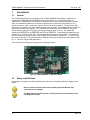
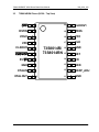
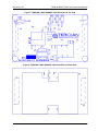
Simplifying System IntegrationTM
73S8014R/RN/RT 20SO
Demo Board User Manual
July, 2008
Rev. 1.0
UM_8014_010
73S8014R/RN/RT 20SO Demo Board User Manual
UM_8014_010
© 2008 Teridian Semiconductor Corporation. All rights reserved.
Teridian Semiconductor Corporation is a registered trademark of Teridian Semiconductor Corporation.
Simplifying System Integration is a trademark of Teridian Semiconductor Corporation.
All other trademarks are the property of their respective owners.
Teridian Semiconductor Corporation makes no warranty for the use of its products, other than expressly
contained in the Company’s warranty detailed in the Teridian Semiconductor Corporation standard Terms
and Conditions. The company assumes no responsibility for any errors which may appear in this
document, reserves the right to change devices or specifications detailed herein at any time without
notice and does not make any commitment to update the information contained herein. Accordingly, the
reader is cautioned to verify that this document is current by comparing it to the latest version on
http://www.teridian.com or by checking with your sales representative.
Teridian Semiconductor Corp., 6440 Oak Canyon, Suite 100, Irvine, CA 92618
TEL (714) 508-8800, FAX (714) 508-8877, http://www.teridian.com
2
Rev. 1.0
UM_8014_010
73S8014R/RN/RT 20SO Demo Board User Manual
Table of Contents
1 Introduction ......................................................................................................................................... 4 1.1 General ......................................................................................................................................... 4 1.2 Safety and ESD Notes .................................................................................................................. 4 1.3 Getting Started .............................................................................................................................. 5 1.4 Recommended Operating Conditions and Absolute Maximum Ratings ...................................... 6 1.4.1 Recommended Operating Conditions ....................................................................................... 6 1.4.1 Absolute Maximum Ratings: ...................................................................................................... 6 2 Design Considerations ....................................................................................................................... 9 2.1 General Layout Rules ................................................................................................................... 9 2.2 Optimization for Compliance with NDS......................................................................................... 9 3 Use of the Board: Hardware ............................................................................................................ 10 3.1 Board Description: Jumpers, Switches and Test Points ............................................................. 10 3.2 73S8014R/RN/RT Pin Description.............................................................................................. 12 3.3 73S8014R/RN Pinout (SO20 – Top View) .................................................................................. 14 3.4 73S8014RT PINOUT (20SO – Top View) .................................................................................. 15 4 Appendix ............................................................................................................................................ 16 6 Contact Information .......................................................................................................................... 23 Rev. 1.0
3
73S8014R/RN/RT 20SO Demo Board User Manual
1
Introduction
1.1
General
UM_8014_010
The TERIDIAN Semiconductor Corporation (TSC) 73S8014R/RN/RT Demo Board is a platform for
evaluating the TERIDIAN 73S8014R/RN/RT smart card interface ICs. It incorporates either the
73S8014R, the 73S8014RN or the 73S8014RT integrated circuit, and it has been designed to operate
either as a standalone platform (to be used in conjunction with an external microcontroller) or as a
daughter card to be used in conjunction with the 73S12xxF evaluation platform. The three parts differ
only slightly with regard to the control signals and the control function. These differences involve the VCC
and the clock divider control signals. The 73S8014R and 73S8014RN use the CMDVCC and 5V/#V
control signals to generate VCC (smart card supply voltage) at either 3V or 5V. The 73S8014RT
redefines the CMDVCC pin as CMDVCC% and 5V/#V as CMDVCC#. These redefined signals allow the
selection of 5V, 3V and 1.8V for VCC. See the applicable data sheet for further detail. The 73S8014R
uses the clock divider signals CLKDIV1 and CLKDIV2 to select between a divide by 1, 2, 4 and 8 for the
smart card CLK output. The 73S8014RN and 73S8014RT have been redefined to select between divide
by 1, 2, 4 and 6 to support NDS applications.
The board has been designed to comply with the NDS specification.
Figure 1: 73S8014R/RN/RT 20 SO Demo Board
1.2
Safety and ESD Notes
Connecting live voltages to the Demo Board system will result in potentially hazardous voltages on the
boards.
Extreme caution should be taken when handling the Demo Boards after
connection to live voltages!
The Demo Boards are ESD sensitive! ESD precautions should be taken when
handling these boards!
4
Rev. 1.0
UM_8014_010
1.3
73S8014R/RN/RT 20SO Demo Board User Manual
Getting Started
The Figure 1.1 shows the basic connections of the Demo Board.
•
•
•
•
Power Supplies: Apply 3.3V to pin 10 of J4 and 5V to pin 10 of J2.
Control signals to the device can be connected through J2 and J4 (see Figure 1.1 and the electrical
schematic Figure 4.1)
Setting the clock frequency with an external clock source
o Set JP1 to the SCLK setting
o Apply clock source to pin 1 of J2
o Apply 3.3V (1) or GND (0) to CLKDIV1 and CLKDIV2 pins allows the following:
- CLKDIV1 = CLKDIV2 = 0
- 73S8014R clock frequency = SCLK/8
- 73S8014RN/RT clock frequency = SCLK/6
- CLKDIV1 = 0, CLKDIV2 =1 clock frequency = SCLK/4 (all)
- CLKDIV1 = 1, CLKDIV2 =0 clock frequency = SCLK (all)
- CLKDIV1 = CLKDIV2 = 1 clock frequency = SCLK/2 (all)
Setting the clock frequency using crystal Y1
o Crystal included in the Demo Board is 12MHz (NDS applications can use 27MHz)
o Set JP1 to XTAL position
o Apply 3.3V (1) or GND (0) to CLKDIV1 and CLKDIV2 pins allows the following:
- CLKDIV1 = CLKDIV2 = 0
9 12MHz XTAL – clock frequency = 1.5MHz
9 27MHz XTAL – clock frequency = 4.5MHz
- CLKDIV1 = 0, CLKDIV2 =1 clock frequency = 3MHz
9 12MHz XTAL – clock frequency = 3MHz
9 27MHz XTAL – clock frequency = 6.75MHz
- CLKDIV1 = 1, CLKDIV2 = 0 – clock frequency = 12MHz
9 12MHz XTAL – clock frequency = 12MHz
9 27MHz XTAL – Illegal setting. Clock is not guaranteed to be stable as the device spec
max CLK frequency is 20MHz.
-
Rev. 1.0
CLKDIV1 = CLKDIV2 = 1 clock frequency = 6MHz
9 12MHz XTAL – clock frequency = 6MHz
9 27MHz XTAL - clock frequency = 13.5MHz
5
73S8014R/RN/RT 20SO Demo Board User Manual
1.4
UM_8014_010
Recommended Operating Conditions and Absolute Maximum Ratings
1.4.1 Recommended Operating Conditions
Parameter
Rating
Supply Voltage VDD
2.7 to 5.5 VDC
Supply Voltage VPC
4.75 to 5.5 VDC (ISO-7816 and EMV applications)
4.85V to 5.5 VDC (NDS applications)
Ambient Operating Temperature
-40°C to +85°C
Input Voltage for Digital Inputs
0V to VDD + 0.3V
1.4.1 Absolute Maximum Ratings:
Operation outside these rating limits may cause permanent damage to the device.
Parameter
Rating
Supply Voltage VDD
-0.5 to 6.0 VDC
Supply Voltage VPC
-0.5 to 6.0 VDC
Input Voltage for Digital Inputs
-0.3 to (VDD+0.5) VDC
Storage Temperature
-60 to 150°C
Pin Voltage
-0.3 to (VDD+0.5) VDC
Pin Current
±100mA
ESD Tolerance – Card interface pins
+/- 6kV
ESD Tolerance – Other pins
+/- 2kV
Note: ESD testing on Card pins is HBM condition, 3 pulses, each polarity referenced to ground.
6
Rev. 1.0
UM_8014_010
73S8014R/RN/RT 20SO Demo Board User Manual
External clock source. JP1
must be in position SCLK
when use of an external
clock. Otherwise, pin
SCLK can be left open.
1
SCLK
VDD Power Supply:
+2.7V to +3.6V
(3.3V Typ.) / 50mA
VDD
GND
IOUC
RSTIN
CMDVCC / CMDVCC%
OFF
GND
5V/#V / CMDVCC#
CKDIV2
2
CKDIV1
VPC
VPC Power
Supply:
+4.5V to +5.5V
(5V Typ.)
/200mA
Figure 2: 73S8014R/RN/RT Demo Board: Basic Connections
Rev. 1.0
7
UM_8014_010
2
Design Considerations
2.1
General Layout Rules
73S8014R/RN/RT 20SO Demo Board User Manual
Keep the CLK signal as short as possible and with few bends in the trace. Keep route of the CLK trace to
one layer (avoid vias to other plane). Keep CLK trace away from other traces especially RST and VCC.
Filtering of the CLK trace is allowed for noise purpose. Up to 30pF to ground is allowed at the CLK pin of
the smart card connector. Also, the 0Ω series resistor, R7, can be replaced for additional filtering (no
more than 100Ω).
Keep the VCC trace as short as possible. Make trace a minimum of 0.5mm thick. Also, keep VCC away
from other traces especially RST and CLK.
Keep RST trace away from VCC and CLK traces. Up to 30pF to ground is allowed for filtering.
Keep 0.1μF close to the VDD pin of the device and directly take other end to ground.
Keep 0.1μF and 10μF close to the VPC pin of the device and directly take other end to ground.
Keep 1.0μF close to the VCC pin of the smart card connector and directly take other end to ground
2.2
Optimization for Compliance with NDS
Default configuration of the Demo Board contains a 27pF capacitor (C12) from the CLK pin of the smart
connector to ground and a 27pF capacitor (C9) from the RST pin of the smart connector to ground.
These capacitors serve as filters for the CLK and RST signals in the case of long traces or test equipment
perturbations. The capacitor on CLK reduces ringing on the trace, reduces coupling to other traces and
slows down the edge of the CLK signal. The capacitor on RST helps the perturbation specification in a
noisy environment. The filter capacitors can be useful in the EMV test environment and have no effect on
NDS testing
C12 and C9 are represented on both the schematic and BOM. These capacitors are optional filter
capacitors on the smart card lines CLK and RST, respectively for each card interface. These capacitors
may be adjusted (value, not to exceed 30pF) or removed to optimize performance in each specific
application (PCB, card clock frequency, compliance with applicable standards, etc.).
Rev. 1.0
9
73S8014R/RN/RT 20SO Demo Board User Manual
3
Use of the Board: Hardware
3.1
Board Description: Jumpers, Switches and Test Points
UM_8014_010
The items described in the following tables refer to the flags in Figure 2.1
Table 1: Demo Board Description
Item #
(Figure
2.1)
Schemati
c & PCB
Silk-print
Reference
1
Name
Use
J2
Board 5V
supply and
host digital
interface
Connector that gathers the 5V supply of the board, the
73S8014R/RN/RT data interface (IOUC), external clock (SCLK)
and interrupt (OFF) pins. Note that the external clock (SCLK) can
be left open when JP1 is in position XTAL.
Also note that the 5V power supply pin can be left open when JP2
is in position 3.3V (= support of 3V cards only).
2
JP3
VDD Select
Jumper to select the digital voltage, between 5V or 3.3V This
setting defines the interfacing voltage with the host microcontroller.
It also provides internal supply voltage for internal circuitry to the
73S8014R/RN/RT.
The default setting is in the 3.3V position.
3
4
5
9
TP7
TP5
TP3
TP4
Test Points:
CLK
RST
VCC
I/O
6
J4
Board 3.3V
supply and
digital control
signals
Connector that gathers the 3.3V supply of the board, the
73S8014R/RN/RT host control signal pins RSTIN, CMDVCC /
CMDVCC%, 5V/#V / CMDVCC#, CLKDIV2 and CLKDIV1.
Note that the 3.3V power supply pin can be left open when JP3 is
in position 5V.
7
TP1
PIN12
(VDDF_ADJ)
VDD voltage fault adjustment. Pin to the left is connected to the
VDDF_ADJ pin of the 73S8014R/RN/RT and the pin to the right is
GND. When either a resistor R3, or a resistor network R1 and R3
is populated on the board, it adjusts the VDD fault level that
internally triggers a card deactivation sequence.
By default, the resistors R1 and R3 are not connected. It provides
a VDD fault level of 2.3V typical (internally set to the
73S8014R/RN/RT).
Refers to the 73S8014R/RN/RT Data Sheet for further information
about VDD fault level and determination of these resistor values.
8
J6
Smart Card
Connector
SIM/SAM smart card format connector.
Note that J6 is wired is parallel to the smart card connector J5
(underneath the PCB). No SIM/SAM should be inserted when
using the credit-card size connector J5.
10
JP1
Clock
selection.
Jumper to select between a crystal and external clock as the
frequency reference to the device. The default setting is for a
crystal.
11
J5
Smart Card
Connector
Smart card connector.
When inserting a card (credit card size format), contacts must face
up.
10
2-pin test points for each respective smart card signal. The pin
label name is the respective signal (i.e. VCC, CLK) and the other
pin is GND.
Rev. 1.0
UM_8014_010
73S8014R/RN/RT 20SO Demo Board User Manual
4
2
3
5
1
6
7
11
10
9
8
Figure 3: TERIDIAN 73S8014R/RN/RT Demo Board: Board Description
Rev. 1.0
11
73S8014R/RN/RT 20SO Demo Board User Manual
3.2
UM_8014_010
73S8014R/RN/RT Pin Description
Table 2: 73S8014R/RN/RT Pin Description: Card Interface
Name
Pin #
Description
I/O
14
Card I/O: Data signal to/from card. Includes a pull-up resistor to VCC.
RST
15
Card reset: provides reset (RST) signal to card.
CLK
17
Card clock: provides clock signal (CLK) to card. The rate of this clock is
determined by crystal oscillator frequency or external clock input and CLKDIV
selections.
PRES
19
Card Presence switch: active high indicates card is present. Should be tied
to GND when not used, but it Includes a high-impedance pull-down resistor.
VCC
18
Card power supply – logically controlled by sequencer, output of LDO
regulator. Requires an external filter capacitor to the card GND.
GND
16
Card ground
Table 0: 73S8014R/RN/RT Pin Description: Miscellaneous and Outputs
Name
Pin #
Description
XTALIN
9
Crystal oscillator input: can either be connected to the crystal or driven as a
source for the card clock.
XTALOUT
10
Crystal oscillator output: connected to the crystal. Left open if XTALIN is
being used as external clock input.
VDDF_ADJ
12
VDD fault threshold adjustment input: this pin can be used to adjust the VDDF
values (that controls deactivation of the card). Must be left open if unused.
Table 4: 73S8014R/RN/RT Pin Description: Power Supply and Ground
Name
Pin #
VDD
13
System interface supply voltage and supply voltage for internal circuitry.
VPC
4
LDO regulator power supply source.
GND
8, 11
12
Description
Digital ground.
Rev. 1.0
UM_8014_010
73S8014R/RN/RT 20SO Demo Board User Manual
Table 5: 73S8014R/RN/RT Pin Description: Microcontroller Interface
Name
Pin #
Description
(R) - Command VCC (negative assertion): Logic low on this pin causes
the LDO regulator to ramp the VCC supply to the card and initiates a card
activation sequence, if a card is present.
(RN/RT) - Logic low on one or both of these pins will cause the LDO to
ramp the Vcc supply to the smart card and smart card interface to the
value described in the following table
CMDVCC (R)
CMDVCC%
(RN/RT)
6
CMDVCC%
CMDVCC#
0
0
1.8V
0
1
5.0V
1
0
3.0V
1
1
LDO Off
Vcc Output Voltage
Note: In order to set VCC to 1.8V, both CMDVCC% and CMDVCC# must
be asserted low within 400ns of each other. See the Data Sheet for
further details.
5V/#V (R)
CMDVCC#
(RN/RT)
7
(R) - 5 volt / 3 volt card selection: Logic one selects 5 volts for VCC and
card interface, logic low selects 3 volt operation. When the part is to be
used with a single card voltage, this pin should be tied to either GND or
VDD. However, it includes a high impedance pull-up resistor to default this
pin high (selection of 5V card) when not connected.
(RN/RT) See pin 6 above.
CLKDIV1
CLKDIV2
20
5
Sets the divide ratio from the XTAL oscillator (or external clock input) to
the card clock. These pins include pull-down resistors.
CLKDIV1
0
0
1
1
CLKDIV2
0
1
1
0
CLOCK RATE
XTALIN/8 (R) XTALIN/6 (RN/RT)
XTALIN/4
XTALIN/2
XTALIN
OFF
1
Interrupt signal to the processor. Active Low - Multi-function indicating
fault conditions or card presence. Open drain output configuration – It
includes an internal 22kΩ pull-up to VDD.
RSTIN
2
Reset Input: This signal is the reset command to the card.
I/OUC
3
System controller data I/O to/from the card. Includes a pull-up resistor to
VDD.
Rev. 1.0
13
73S8014R/RN/RT 20SO Demo Board User Manual
3.3
73S8014R/RN Pinout (SO20 – Top View)
OFF
1
20
CLKDIV1
RSTIN
2
19
PRES
I/OUC
3
18
VCC
VPC
4
17
CLK
CLKDIV2
5
16
GND
CMDVCC
6
15
RST
5V/#V
7
14
I/O
GND
8
13
VDD
XTALIN
9
12
VDDF_ADJ
10
11
GND
XTALOUT
14
UM_8014_010
73S8014R/
73S8014RN
Rev. 1.0
UM_8014_010
3.4
73S8014R/RN/RT 20SO Demo Board User Manual
73S8014RT PINOUT (20SO – Top View)
OFF
1
20
CLKDIV1
RSTIN
2
19
PRES
I/OUC
3
18
VCC
VPC
4
17
CLK
CLKDIV2
5
16
GND
CMDVCC%
6
15
RST
CMDVCC#
7
14
I/O
GND
8
13
VDD
XTALIN
9
12
VDDF_ADJ
10
11
GND
XTALOUT
Rev. 1.0
73S8014RT
15
73S8014R/RN/RT 20SO Demo Board User Manual
4
UM_8014_010
Appendix
This appendix includes the following tables and drawings of the PCB of the Evaluation Board:
•
•
•
•
•
•
•
•
16
Electrical Schematic
Bill of Materials
Silk Screen Layer – Top side
Silk Screen Layer – Bottom side
Metal Layer – Top side
Metal Layer – Middle 1, ground plane
Metal Layer – Middle 2, supply plane
Metal Layer – Bottom
Rev. 1.0
UM_8014_010
73S8014R/RN/RT 20SO Demo Board User Manual
Figure 4: TERIDIAN 73S8014R/RN/RT 20SO Demo Board: Electrical Schematic
J1
OFFB
GND
GND
GND
+5V
+5V
1
2
3
4
5
6
7
8
9
10
VDD
R1
C1
SSM_110_L_SV
1
2
3
4
5
6
7
8
9
10
C1, C2, C8 and C5 must be
placed within 5mm of the U1
pins and connected by thick
track (wider than 0.5mm)
SCLK
S_C4
S_C8
5.0V
10uF
1
2
3
4
5
6
7
8
9
10
Y1
DNI
0.1uF
3.3V
DNI
JP1
C10
J1 and J3 are placed on the bottom.
are placed on the top side.
OFF
CLKDIV1
RSTIN
PRES
I/OUC
VCC
VPC
CLK
CLKDIV2
GND
CMDVCC/CMDVCC5
RST
5V_3V/CMDVCC3
I/O
GND
VDD
XTALIN
VDDF_ADJ
XTALOUT
GND
20
19
18
17
16
15
14
13
12
11
PRES
VCC
CLK
5.0V
RST
IO
VDD
C5
C4
22pF
22pF
3.3V
VDD
3.3V
JP3
1
2
3
C8
1
12.000MHz
XTALIN
SELECT
+
TSM_110_01_L_SV
1
2
3
J4
XTAL
SCLK
2
SSM_110_L_SV
1
2
3
4
5
6
7
8
9
10
1
2
R3
C6
1
2
3
4
CLKDIV2
5
CMDVCCB/CMDVCC5B6
5V3VB/CMDVCC3B
7
8
XTALIN
9
XTALOUT
10
OFF
RSTIN
I/OUC
J3
CMDVCCB/CMDVCC5B
RSTIN
GND
+3.3V
TP1
U1
C3
TSM_110_01_L_SV
CLKDIV1
CLKDIV2
5V3VB/CMDVCC3B
C2
10uF
VDDF_ADJ
CLKDIV1
+
J2
DNI
5.0V
+
SCLK
SIO
VDD
SELECT
5V
0.1uF
73S8014R(N)/RT
R7
R6
When using an external clock
source, C7 should be removed.
0
20K
10uF
R10
Ru
DNI
R8
Ru
DNI
R9
Ru
DNI
R11
Rd
DNI
R12
Rd
DNI
R8 to R13 and C36 to be
placed within 1cm of
J7.
J2 and J4
R13
Rd
DNI
J1 must be aligned with J2 and J3 must be
aligned with J4 in order for this daughter
board to be stacked on another.
TP3
1
2
TP4
1
2
I/O
VCC
TP5
1
2
RST
TP7
C9
27pF
1
2
TP3 to TP8 to be placed
very close to the pads
of J5
CLK
J5
Rev. 1.0
Smart Card Connector
SW2
SW1
C7
C6
C5
C3
C2
C1
C8
I/O
VPP
GND
C4
CLK
RST
VCC
SW-2
SW-1
8
7
6
5
4
3
2
1
8
7
6
5
4
3
2
1
10
9
C12 VDD
27pF
J6
C11
1.0uF
SIM/SAM Connector
17
73S8014R/RN/RT 20SO Demo Board User Manual
UM_8014_010
Table 6: TERIDIAN 73S8014R/RN/RT 20SO Demo Board: Bill of Material
Item Qty Reference
Part
PCB Footprint
(see attached zip
file)
Digikey Part
Number
Part Number
Manufactuer
1
3
C1, C3, C10
CAP 10UF 6.3V CERAMIC X5R 0805
805
PCC2225CT-ND
ECJ-2FB0J106M
Panasonic
2
1
C11
CAP 1.0UF 6.3V CERAMIC X5R 0603
603
PCC1915CT-ND
ECJ-1VB0J105K
Panasonic
3
2
C2, C8
CAP .1UF 16V CERAMIC X7R 0603
603
PCC1762CT-ND
ECJ-1VB1C104K
Panasonic
4
2
C12, C9
CAP CERAMIC 27PF 50V 0603 SMD
603
PCC270ACVCT-ND ECJ-1VC1H270J
Panasonic
5
2
C4, C5
CAP CERAMIC 22PF 50V 0603 SMD
603
PCC220ACVCT-ND ECJ-1VC1H220J
Panasonic
6
1
R7
RES ZERO OHM 1/10W 5% 0603 SMD
603
P0.0GCT-ND
ERJ-3GEY0R00V
Panasonic
7
1
R6
RES 20K OHM 1/10W 5% 0603 SMD
603
P20KGCT-ND
ERJ-3GEYJ203V
Panasonic
8
1
J6
CONN SMART CARD SIM/SAM 6PIN SMD
ITT_CCM033013
401-1691-1-ND
CCM03-3754
ITT Industries
9
1
J5
CONN SMART CARD 8PIN SMD
CCM02-2504
401-1715-ND
CCM02-2504LFT
ITT Industries
10
5
TP1, TP3,
HEADER 2
TP4, TP5, TP7
2pins, 2.54mm
pich
PZC36SAAN
Sullins
2
JP1, JP3
HEADER 3
3pins, 2.54mm
pich
S1011E-36-ND
11
12
2
J1, J3
SSM_110_L_SV
SSM_110_L_
SV
N/A
SSM_110_L_SV
Samtec
13
2
J2, J4
TSM_110_01_L_SV
TSM_110_01_
N/A
L_SV
TSM_110_01_L_S
Samtec
V
14
1
Y1
CRYSTAL 12.000 MHZ 20PF 49US
HC-49US
ECS-120-20-4DN
ENGYA
15
1
U1
73S8014R/RN/RT
73S8014R/RN/RT
Teridian
Semiconductor
X190-ND
Note: The resistors and capacitors marked DNI are not populated on the board. They can be implemented to adjust the features of the smart card
reader.
18
Rev. 1.0
UM_8014_010
73S8014R/RN/RT 20SO Demo Board User Manual
Figure 5: TERIDIAN 73S8014R/RN/RT 20SO Demo Board: Top View
Figure 6: TERIDIAN 73S8014R/RN/RT 20SO Demo Board: Bottom View
Rev. 1.0
19
73S8014R/RN/RT 20SO Demo Board User Manual
UM_8014_010
Figure 7: TERIDIAN 73S8014R/RN/RT 20SO Demo Board: Top Signal Layer
Figure 8: TERIDIAN 73S8014R/RN/RT 20SO Demo Board: Middle Layer 1, Ground Plane.
20
Rev. 1.0
UM_8014_010
73S8014R/RN/RT 20SO Demo Board User Manual
Figure 9: TERIDIAN 73S8014R/RN/RT 20SO Demo Board: Middle Layer 2, Supply Plane.
Figure 10: TERIDIAN 73S8014R/RN/RT 20SO Demo Board: Bottom Signal Layer
Rev. 1.0
21
UM_8014_010
6
73S8014R/RN/RT 20SO Demo Board User Manual
Contact Information
For more information about Teridian Semiconductor products or to check the availability of the
73S8014R/RN/RT, contact us at:
6440 Oak Canyon Road
Suite 100
Irvine, CA 92618-5201
Telephone: (714) 508-8800
FAX: (714) 508-8878
Email: [email protected]
For a complete list of worldwide sales offices, go to http://www.teridian.com.
23
Rev. 1.0
73S8014R/RN/RT 20SO Demo Board User Manual
UM_8014_010
Revision History
Revision
1.0
24
Date
7/3/2008
Description
First publication.
Rev. 1.0