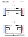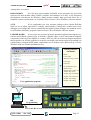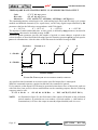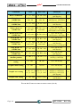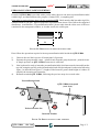
1
QTP 12/R84
Quick Terminal Panel 12 keys,
8 inputs, 4 Relays outputs
USER MANUAL
Via dell' Artigiano, 8/6
® 40016 San Giorgio di Piano
(Bologna) ITALY
ITALIAN TECHNOLOGY
E-mail: [email protected]
http://www.grifo.it
http://www.grifo.com
Tel. +39 051 892.052 (a.r.) FAX: +39 051 893.661
grifo
QTP 12/R84
Rel. 5.00
Edition 03 May 2004
®
®
, GPC , grifo , are trade marks of grifo®
QTP 12/R84
Quick Terminal Panel 12 keys,
8 inputs, 4 Relays outputs
USER MANUAL
Overall dimension: 72x144 mm frontal frame size; 9 mm frontal frame
depth; 28 mm rear metallic housing depth. Remarkably Low Price.
Aluminium container with front plastic frame. Front panel with Keyboard
and display window protected by anti scratch Polyester cover. Case with
rear mounting brackets. Front panel mounting. IP 54 standard protection
on front side. Available with 3 different models of displays: alphanumeric
LCD and VFD with 20x2 chrs. and graphic with 140x16 pixels. Viewing
area size: 82x18 mm. Membrane keypad with 12 keys provided of double
serigraphy: numeric and function. Status LED indicator managed by
software. Panel name, and/or LED indicator, personalization label slot.
Buzzer for acoustic signal driven by software. I51 family microcontroller,
with 14.7 or 29.4 MHz software selectable clock speed. 3 different
memory types: 32K FLASH EPROM; 1,2K RAM; 2K EEPROM. Serial
line configurable in RS 232, RS 422, RS 485 or Current Loop. CAN
communication line provided of proper line driver. 8 optocoupled digital
Inputs, both NPN or PNP type. Some inputs are connected to hardware
counters and Interrupts. 4 relay digital outputs, up to 5 A. Comfortable
quick release, screw terminal connectors for a fast cablation. 2 TTL
I/
O lines on proper connector, suitable for I2C BUS, 1-Wire, SPI, etc.,
devices management. Wide range DC or AC power supply from 5 Vdc to
24 Vac. Total power consumption change according with used
configuration, from 2.5 to 3.3 W. On board protection aganist voltage
peaks by TransZorbTM. Wide range of developement software tools and
programming languages, such as: Assembler; FORTH; PASCAL
Compilers (SYS51PW); C Compilers (HTC 51, SYS51CW, DDS MICRO
C 51, µC/51); Real Time Operating Systems (CMX RTX); Contacts
Logic (Ladder WORK); BASIC compilers (BXC51, BASCOM 8051);
terminal emulation (GET 51), etc. Supplied with two different management
Firmwares: Serial or Library. Customized keyboard and program packages.
Via dell' Artigiano, 8/6
® 40016 San Giorgio di Piano
(Bologna) ITALY
ITALIAN TECHNOLOGY
E-mail: [email protected]
http://www.grifo.it
http://www.grifo.com
Tel. +39 051 892.052 (a.r.) FAX: +39 051 893.661
grifo
QTP 12/R84
Rel. 5.00
Edition 03 May 2004
®
®
, GPC , grifo , are trade marks of grifo®
DOCUMENTATION COPYRIGHT BY grifo® , ALL RIGHTS RESERVED
No part of this document may be reproduced, transmitted, transcribed, stored in a
retrieval system, or translated into any language or computer language, in any form or
by any means, either electronic, mechanical, magnetic, optical, chemical, manual, or
otherwise, without the prior written consent of grifo®.
IMPORTANT
Although all the information contained herein have been carefully verified, grifo®
assumes no responsability for errors that might appear in this document, or for damage
to things or persons resulting from technical errors, omission and improper use of this
manual and of the related software and hardware.
grifo® reserves the right to change the contents and form of this document, as well as the
features and specification of its products at any time, without prior notice, to obtain
always the best product.
For specific informations on the components mounted on the card, please refer to the
Data Book of the builder or second sources.
SYMBOLS DESCRIPTION
In the manual could appear the following symbols:
Attention: Generic danger
Attention: High voltage
Attention: ESD sensitive device
Trade Marks
, GPC®, grifo® : are trade marks of grifo®.
Other Product and Company names listed, are trade marks of their respective companies.
grifo®
ITALIAN TECHNOLOGY
GENERAL INDEX
INTRODUCTION ........................................................................................................................ 1
HARDWARE AND FIRMWARE VERSION ............................................................................ 2
GENERAL INFORMATION ...................................................................................................... 2
SERIAL LINE ............................................................................................................................ 4
INDICATOR LED ..................................................................................................................... 6
DISPLAY .................................................................................................................................... 6
KEYBOARD .............................................................................................................................. 6
BUZZER ..................................................................................................................................... 7
MEMORY DEVICES ................................................................................................................ 7
ON BOARD POWER SUPPLY ............................................................................................... 7
MICROCONTROLLER .......................................................................................................... 8
CAN INTERFACE .................................................................................................................... 8
TTL I/O LINES .......................................................................................................................... 8
OPTOCOUPLED DIGITAL INPUTS ..................................................................................... 8
RELAYS DIGITAL OUTPUTS ................................................................................................ 8
TECHNICAL FEATURES ........................................................................................................ 10
GENERAL FEATURES .......................................................................................................... 10
PHYSICAL FEATURES ......................................................................................................... 11
ELECTRIC FEATURES ........................................................................................................ 12
INSTALLATION ........................................................................................................................ 14
CONNECTIONS ..................................................................................................................... 14
CN1 - POWER SUPPLY CONNECTOR ........................................................................... 14
CN2 - SERIAL LINE CONNECTOR ................................................................................. 16
CN3 - CAN INTERFACE CONNECTOR ......................................................................... 22
CN4 - RELAYS DIGITAL OUPUTS CONNECTOR ....................................................... 24
CN5 - OPTOCOUPLED DIGITAL INPUTS CONNECTOR .......................................... 26
J6 - TTL I/O, 1-WIRE, I2C BUS CONNECTOR .............................................................. 28
CONTRAST REGULATION TRIMMER ............................................................................ 30
JUMPERS ................................................................................................................................ 30
SERIAL LINE CONFIGURATION ...................................................................................... 32
CAN INTERFACE CONNECTION ...................................................................................... 34
INTERRUPTS ......................................................................................................................... 35
CONNECTOR SIGNALS INTERFACEMENT .................................................................. 35
POWER SUPPLY .................................................................................................................... 36
SOFTWARE DESCRIPTION ................................................................................................... 38
DATA STORED ON EEPROM .............................................................................................. 38
CHARACTERS VISUALIZATION ON DISPLAY ............................................................. 39
RECEIVE BUFFER ................................................................................................................ 40
KEYBOARD ACQUISITION ................................................................................................ 40
KEYS CODES ...................................................................................................................... 40
QTP 12/R84
Rel. 5.00
Page I
grifo®
ITALIAN TECHNOLOGY
SERIAL FIRMWARE .SER ................................................................................................... 42
LOCAL SET UP WITH SERIAL FRIRMWARE ............................................................. 42
COMMUNICATION MODALITIES WITH SERIAL FIRMWARE ............................. 43
MASTER SLAVE COMMUNICATION MODE .............................................................. 43
HOW TO START WITH SERIAL FIRMWARE .............................................................. 46
DEMO PROGRAMS FOR SERIAL FIRMWARE ........................................................... 47
LIBRARY FIRMWARE .LIB ................................................................................................ 48
INTEGRATION AND USE OF LIBRARY FIRMWARE ................................................ 48
RESOURCES USED BY LIBRARY FIRMWARE ........................................................... 52
FLASH EPROM PROGRAMMING ................................................................................. 54
DEVELOPMENT SOFTWARE FOR LIBRARY FIRMWARE ..................................... 54
HOW TO START WITH LIBRARY FIRMWARE .......................................................... 56
DEMO PROGRAMS FOR LIBRARY FIRMWARE ....................................................... 60
COMMANDS .............................................................................................................................. 61
COMMANDS FOR CURSOR POSITION ........................................................................... 61
CURSOR LEFT .................................................................................................................... 61
CURSOR RIGHT ................................................................................................................. 61
CURSOR DOWN ................................................................................................................. 61
CURSOR UP ......................................................................................................................... 62
HOME ................................................................................................................................... 62
CARRIAGE RETURN ........................................................................................................ 62
CARRIAGE RETURN+LINE FEED ................................................................................. 62
ABSOLUTE PLACEMENT OF ALPHANUMERIC CURSOR ..................................... 62
COMMANDS FOR CHARACTERS ERASURE ................................................................ 63
BACKSPACE ........................................................................................................................ 63
CLEAR PAGE ...................................................................................................................... 63
CLEAR LINE ....................................................................................................................... 63
CLEAR END OF LINE........................................................................................................ 63
CLEAR END OF PAGE ...................................................................................................... 63
COMMANDS FOR EEPROM ............................................................................................... 64
REQUEST FOR EEPROM AVAILABILITY .................................................................... 64
WRITE OF PRESENCE BYTE .......................................................................................... 64
READING OF PRESENCE BYTE ..................................................................................... 64
WRITE BYTE ON EEPROM ............................................................................................. 65
READ BYTE FROM EEPROM ......................................................................................... 65
COMMANDS FOR GENERAL FUNCTIONS .................................................................... 66
READ FIRMWARE VERSION .......................................................................................... 66
READ CARD CODE ............................................................................................................ 66
FLUORESCENT DISPLAY BRIGHTNESS SETTING .................................................. 66
OPERATING MODE SELECTION .................................................................................. 67
COMMUNICATION RESET ............................................................................................. 67
GENERAL RESET .............................................................................................................. 67
BEEP ...................................................................................................................................... 68
LED AND BUZZER ACTIVATION ................................................................................... 68
COMMANDS FOR MESSAGE MANAGEMENT ............................................................. 69
READING OF MAX MESSAGE NUMBER ..................................................................... 69
MESSAGE STORAGE ........................................................................................................ 69
MESSAGE READING ......................................................................................................... 70
Page II
QTP 12/R84
Rel. 5.00
ITALIAN TECHNOLOGY
grifo®
VISUALIZATION OF N MESSAGES ............................................................................... 70
SCROLLING MESSAGES VISUALIZATION ................................................................ 71
COMMANDS FOR KEYBOARD MANAGEMENT .......................................................... 72
KEY CODE RECONFIGURATION .................................................................................. 72
KEYCLICK ON WITHOUT MEMORIZATION ............................................................ 72
KEYCLICK OFF WITHOUT MEMORIZATION .......................................................... 72
KEYCLICK ON WITH MEMORIZATION ..................................................................... 73
KEYCLICK OFF WITH MEMORIZATION ................................................................... 73
COMMANDS FOR USER CHARACTERS ......................................................................... 74
DEFINITION OF USER CHARACTER ........................................................................... 75
DEFINITION AND MEMORIZATION OF USER CHARACTER ............................... 75
COMMANDS FOR CURSOR ATTRIBUTES MANAGEMENT ...................................... 76
CURSOR OFF ...................................................................................................................... 76
STEADY STATIC CURSOR ON ........................................................................................ 76
BLINKING BLOCK CURSOR ON ................................................................................... 76
COMMANDS FOR BUFFERED DIGITAL I/OS MANAGEMENT ................................. 77
WRITE ALL DIGITAL OUTPUTS .................................................................................... 77
ACQUIRE ALL DIGITAL INPUTS ................................................................................... 77
ENABLE SINGLE DIGITAL OUTPUT ............................................................................ 78
TIMED ENABLE OF SINGLE DIGITAL OUTPUT ....................................................... 78
DISABLE SINGLE DIGITAL OUTPUT ........................................................................... 79
TIMED DISABLE OF SINGLE DIGITAL OUTPUT ...................................................... 79
ACQUIRE SINGLE DIGITAL INPUT .............................................................................. 80
ACQUIRE SINGLE DIGITAL INPUT WITH DEBOUNCING ..................................... 80
TIMED SQARE WAVE STARTING WITH "1" ON SINGLE DIGITAL OUTPUT .... 81
TIMED SQARE WAVE STARTING WITH "0" ON SINGLE DIGITAL OUTPUT .... 82
SQARE WAVE ON SINGLE DIGITAL OUTPUT ........................................................... 83
COMMANDS FOR ALTERNATIVE FUNCTIONS OF DIGITAL I/OS .......................... 84
SET MULTIFUNCTIONS PINS ......................................................................................... 84
READ MULTIFUNCTIONS PINS SETTING .................................................................. 84
READ COUNTER ................................................................................................................ 85
RESET COUNTER .............................................................................................................. 85
GRAPHIC COMMANDS ....................................................................................................... 86
ALPHANUMERIC MODE SETTING ............................................................................... 86
GRAPHIC MODE SETTING ............................................................................................. 88
GRAPHIC CURSOR ABSOLUTE POSITION ................................................................ 88
GRAPHIC AREA SETTING ............................................................................................... 88
GRAPHIC FONT SETTING .............................................................................................. 92
COMMAND FOR 1-WIRE COMMUNICATION .............................................................. 93
RESET 1-WIRE LINE ......................................................................................................... 94
WRITE BIT ON 1-WIRE LINE ......................................................................................... 94
READ BIT FROM 1-WIRE LINE ...................................................................................... 94
WRITE N BYTES ON 1-WIRE LINE ............................................................................... 95
READ N BYTES FROM 1-WIRE BUS ............................................................................. 95
"READ ROM" ON 1-WIRE LINE .................................................................................... 96
"SKIP ROM" ON 1-WIRE LINE ....................................................................................... 96
"MATCH ROM" ON 1-WIRE LINE ................................................................................. 97
"ALARM SERCH" ON 1-WIRE LINE ............................................................................. 98
QTP 12/R84
Rel. 5.00
Page III
grifo®
ITALIAN TECHNOLOGY
EXTERNAL CARDS ................................................................................................................. 99
BIBLIOGRAPHY ..................................................................................................................... 102
APPENDIX A: COMMANDS SUMMARY TABLES ........................................................... A-1
APPENDIX B: DISPLAY CHARACTERS ........................................................................... B-1
APPENDIX C: MOUNTING NOTES .................................................................................... C-1
TERMINAL DIMENSIONS ................................................................................................. C-1
FRONT PANEL MOUNTING ............................................................................................. C-2
PERSONALIZATION LABEL INSERTION ..................................................................... C-3
FIXING FRONTAL PANEL TO CONTAINER ................................................................. C-4
APPENDIX D: DATA SHEETS .............................................................................................. D-1
T89C51CC01 AND T89C51AC2 .......................................................................................... D-1
APPENDIX E: ALPHABETICAL INDEX ............................................................................ E-1
Page IV
QTP 12/R84
Rel. 5.00
grifo®
ITALIAN TECHNOLOGY
FIGURES INDEX
FIGURE 1: BLOCKS DIAGRAM ............................................................................................................ 3
FIGURE 2: PHOTO OF AVAILABLE MODELS .......................................................................................... 5
FIGURE 3: QTP 12/R84 COMPLETE PHOTO ...................................................................................... 9
FIGURE 4: CONSUMPTIONS TABLE ................................................................................................... 12
FIGURE 5: QTP 12/R84-C2 PHOTO ............................................................................................... 13
FIGURE 6: QTP 12/R84-F2 PHOTO ............................................................................................... 13
FIGURE 7: QTP 12/R84-GF2 PHOTO ............................................................................................ 13
FIGURE 8: CN1 - POWER SUPPLY CONNECTOR ................................................................................ 14
FIGURE 9: AC POWER SUPPLY CONNECTION 8 ÷ 24 VAC ±5% ........................................................ 15
FIGURE 10: DC POWER SUPPLY CONNECTION +10 ÷ 40 VDC ±5% ................................................. 15
FIGURE 11: STABILIZED POWER SUPPLY CONNECTION +5 VDC ±5% ................................................ 15
FIGURE 12: CN2 - SERIAL LINE CONNECTOR .................................................................................. 16
FIGURE 13: SERIAL COMMUNICATION DIAGRAM ............................................................................... 17
FIGURE 14: RS 232 POINT TO POINT CONNECTION EXAMPLE ........................................................... 18
FIGURE 15: RS 422 POINT TO POINT CONNECTION EXAMPLE ........................................................... 18
FIGURE 16: RS 485 POINT TO POINT CONNECTION EXAMPLE ........................................................... 18
FIGURE 17: RS 485 NETWORK CONNECTION EXAMPLE .................................................................... 19
FIGURE 18: CURRENT LOOP 4 WIRES POINT TO POINT CONNECTION EXAMPLE ................................... 20
FIGURE 19: CURRENT LOOP 2 WIRES POINT TO POINT CONNECTION EXAMPLE ................................... 20
FIGURE 20: CURRENT LOOP NETWORK CONNECTION EXAMPLE ......................................................... 21
FIGURE 21: CN3 - CAN INTERFACE CONNECTOR ........................................................................... 22
FIGURE 22: CAN LINE CONNECTION .............................................................................................. 22
FIGURE 23: CAN NETWORK CONNECTION EXAMPLE ....................................................................... 23
FIGURE 24: CN4 - RELAYS DIGITAL OUTPUTS CONNECTOR .............................................................. 24
FIGURE 25: RELAYS OUTPUTS CONNECTION ..................................................................................... 24
FIGURE 26: RELAYS OUTPUTS BLOCK DIAGRAM ............................................................................... 25
FIGURE 27: CN5 - OPTOCOUPLED DIGITAL INPUTS CONNECTOR ...................................................... 26
FIGURE 28: OPTOCOUPLED INPUTS BLOCK DIAGRAM ....................................................................... 27
FIGURE 29: OPTOCOUPLED INPUTS CONNECTION ............................................................................. 27
FIGURE 30: TTL I/O, 1-WIRE, I2C BUS CONNECTOR ................................................................ 28
FIGURE 31: TTL I/O, 1-WIRE, I2C BUS BLOCK DIAGRAM ......................................................... 28
FIGURE 32: JUMPERS, CONNECTORS, TRIMMER, ETC LOCATION. ....................................................... 29
FIGURE 33: JUMPERS TABLE ........................................................................................................... 30
FIGURE 34: COMPONENTS MAP SOLDER SIDE ................................................................................... 31
FIGURE 35: COMPONENTS MAP COMPONENTS SIDE .......................................................................... 31
FIGURE 36: DRIVERS LOCATION FOR SERIAL COMMUNICATION ......................................................... 33
FIGURE 37: POWER SUPPLY EXPS-2 PHOTO ................................................................................... 37
FIGURE 38: PHOTO OF CHARACTERS AVAILABLE ON QTP 12/R84-GF2 .......................................... 39
FIGURA 39: KEYS NUMERATION AND LOCATION ............................................................................... 41
FIGURE 40: DEFAULT KEYS CODES .................................................................................................. 41
FIGURE 41: MASTER SLAVE PROTOCOL COMMUNICATION EXAMPLE .................................................. 45
FIGURE 42: RS 232 CONNECTION WITH P.C. AND SERIAL FIRMWARE ............................................... 46
FIGURE 43: CODE AREA ORGANIZATION WITH LIBRARY FIRMWARE ................................................... 49
FIGURE 44: RAM USE WITH LIBRARY FIRMWARE ............................................................................ 51
FIGURE 45: DEVELOPMENT MODE WITH LIBRARY FIRMWARE ........................................................... 55
FIGURE 46: RS 232 CONNECTION WITH P.C. AND LIBRARY FIRMWARE ............................................ 56
QTP 12/R84
Rel. 5.00
Page V
grifo®
ITALIAN TECHNOLOGY
FIGURE 47: FLIP SETTINGS WINDOW (1 OF 4) ................................................................................ 57
FIGURE 48: FLIP SETTINGS WINDOW (2 OF 4) ................................................................................ 58
FIGURE 49: FLIP SETTINGS WINDOW (3 OF 4) ................................................................................ 58
FIGURE 50: FLIP SETTINGS WINDOW (4 OF 4) ................................................................................ 59
FIGURE 51: PHOTO OF FRONTAL WITH KEYBOARD ........................................................................... 73
FIGURE 52: USER CHARACTERS PATTERN ........................................................................................ 74
FIGURE 53: TIMED ENABLE OF SINGLE DIGITAL OUTPUT, COMMAND ................................................. 78
FIGURE 54: TIMED DISABLE OF SINGLE DIGITAL OUTPUT, COMMAND ................................................. 79
FIGURE 55: TIMED SQARE WAVE STARTING WITH 1, COMMAND ......................................................... 81
FIGURE 56: TIMED SQARE WAVE STARTING WITH 0, COMMAND ......................................................... 82
FIGURE 57: SQARE WAVE, COMMAND .............................................................................................. 83
FIGURE 58: COORDINATES OF GRAPHIC DISPLAY PIXELS ................................................................... 86
FIGURE 59: FIRST GRAPHIC EXAMPLE ............................................................................................. 87
FIGURE 60: SECOND GRPHIC EXAMPLE ............................................................................................ 87
FIGURE 61: EXAMPLE OF GRAPHIC DRAWING ................................................................................... 89
FIGURE 62: HORIZONTAL GRAPHIC DATA AND HORIZONTAL SHIFT ..................................................... 90
FIGURE 63: HORIZONTAL GRAPHIC DATA AND VERTICAL SHIFT ......................................................... 90
FIGURE 64: VERTICAL GRAPHIC DATA AND HORIZONTAL SHIFT ......................................................... 91
FIGURE 65: VERTICAL GRAPHIC DATA AND VERTICAL SHIFT ............................................................. 91
FIGURE 66: CONNECTION EXAMPLE WITH TWO 1-WIRE DEVICES .................................................. 93
FIGURE 67: FUNCTIONAL DIAGRAM OF 1-WIRE PROTOCOL ............................................................ 97
FIGURE 68: AVAILABLE CONNECTIONS DIAGRAM ........................................................................... 101
FIGURE A1: COMMAND CODES SUMMARY TABLE (1 OF 4) .............................................................. A-1
FIGURE A2: COMMAND CODES SUMMARY TABLE (2 OF 4) .............................................................. A-2
FIGURE A3: COMMAND CODES SUMMARY TABLE (3 OF 4) .............................................................. A-3
FIGURE A4: COMMAND CODES SUMMARY TABLE (4 OF 4) .............................................................. A-4
FIGURE B1: QTP 12/R84-F2, GF2 CHARACTERS TABLE, IN ALPHANUMERIC MODE ...................... B-1
FIGURE B2: QTP 12/R84-C2 CHARACTERS TABLE ...................................................................... B-2
FIGURE B3: QTP 12/R84-GF2 MINIFONT CHARACTERS TABLE, IN GRAPHIC MODE ...................... B-3
FIGURE B4: QTP 12/R84-GF2 KATAKANA FONT CHARACTERS TABLE, IN GRAPHIC MODE ............ B-4
FIGURE B5: QTP 12/R84-GF2 EUROPEAN FONT CHARACTERS TABLE, IN GRAPHIC MODE ............. B-5
FIGURE C1: DIMENSIONS QTP 12/R84 ....................................................................................... C-1
FIGURE C2: BREAKING FOR INSTALLATION ................................................................................... C-2
FIGURE C3: DIMENSIONS OF PERSONALIZATION LABEL .................................................................. C-3
FIGURE C4: PERSONALIZATION LABEL INSERTION ......................................................................... C-3
Page VI
QTP 12/R84
Rel. 5.00
ITALIAN TECHNOLOGY
grifo®
INTRODUCTION
The use of these devices has turned - IN EXCLUSIVE WAY - to specialized personnel.
This device is not a safe component as defined in directive 98-37/CE.
Pins of module are not provided with any kind of ESD protection. Many pins of the card are directly
connected to their respective pins of on board's components and these last are sensitive to
electrostatic noises. So personnel who handles the product is invited to take all necessary precautions
that avoid possible damages caused by electrostatic discharges.
The purpose of this handbook is to give the necessary information to the cognizant and sure use of
the products. They are the result of a continual and systematic elaboration of data and technical tests
saved and validated from the manufacturer, related to the inside modes of certainty and quality of
the information.
The reported data are destined- IN EXCLUSIVE WAY- to specialized users, that can interact with
the devices in safety conditions for the persons, for the machine and for the enviroment, impersonating
an elementary diagnostic of breakdowns and of malfunction conditions by performing simple
functional verify operations , in the height respect of the actual safety and health norms.
The informations for the installation, the assemblage, the dismantlement, the handling, the adjustment,
the reparation and the contingent accessories, devices etc. installation are destined - and then
executable - always and in exclusive way from specialized warned and educated personnel, or
directly from the TECHNICAL AUTHORIZED ASSISTANCE, in the height respect of the
manufacturer recommendations and the actual safety and health norms.
The devices can't be used outside a box. The user must always insert the cards in a container that
rispect the actual safety normative. The protection of this container is not threshold to the only
atmospheric agents, but specially to mechanic, electric, magnetic, etc. ones.
To be on good terms with the products, is necessary guarantee legibility and conservation of the
manual, also for future references. In case of deterioration or more easily for technical updates,
consult the AUTHORIZED TECHNICAL ASSISTANCE directly.
To prevent problems during card utilization, it is a good practice to read carefully all the informations
of this manual. After this reading, the user can use the general index and the alphabetical index,
respectly at the begining and at the end of the manual, to find information in a faster and more easy
way.
QTP 12/R84
Rel. 5.00
Page 1
grifo®
ITALIAN TECHNOLOGY
HARDWARE AND FIRMWARE VERSION
This handbook make reference to printed circuit version 100403 and to firmware version 1.3 and
following ones. The validity of the information contained in this manual is subordinated to the
firmware release number, so the user must always verify the correct correspondence beetween the
notations. The printed circuit version is reported in several places, for example over the serial
connector CN2 on the component side. Inside the device, the firmware release number is written on
the label stuck on the CPU or it can be obtained by a proper command.
GENERAL INFORMATION
QTP 12/R84 is a powerfull module complete of inputs, outputs and operator interface. It contains
a complete PLC controller capable to manage completely a specific application in a minimun size,
specifically designed for industrial and/or domestic use.
QTP 12/R84 is available with alphanumeric displays by 20 characters for 2 lines in two different
types: LCD type with LED backligt or Fluorescent, or alternatively with graphic Fluorescent display
with 140x16 pixels. In addition on the front panel there are: a 12 keys membrane keyboard, a label
slot used to carry a name for the QTP 12/R84 or the user's own logo, and a status LED.
A pratical and robust metallic container, in the standard DIN 72x144 size allows a direct mounting
in front panel modality with a protected front side and back openings for connections. The enclosed
brackets supplied with QTP 12/R84 let the user mount and/or unmount the terminal by performing
a simple rectangle digging up on the support panel. Alternatively it can be used on a table with no
elements addition.
The module's serial line can be buffered with the most frequently used electric protocols and thanks
to this feature the QTP 12/R84 can be connected to each systems available on the market and
moreover low cost networks can be realized where many different units can be contemporaneously
managed. The interconnection with other devices is ensured also by the optional CAN line, that
increase the possible applications fields and gives better performance of the cemplete network.
CPU section features 32K FLASH with ISP interface for comfortable programming through serial
line; this allows an easy development environment that doesn't require any additional system, with
a considerable cost reductions. The user can write the application program with 8051 compatible
code, by using one of the numerous high level development tools as the convenient BASIC compiler
BASCOM 8051; the efficient C compiler µC/51 or the well known LadderWORK for the users that
want contacts programming. Moreover are available different ready to use management firmwares
for faster and easier development, that are briefly described below.
Hardware features of QTP 12/R84, including possible options, are as follows:
- Overall dimension: 72x144 mm frontal frame size; 9 mm frontal frame depth; 28 mm
rear metallic housing depth.
- Remarkably low price.
- Aluminium container with front plastic frame.
- Front panel with Keyboard and display window protected by anti scratch Polyester
cover.
- Case with rear mounting brackets.
- Front panel mounting.
- IP 54 standard protection on front side.
Page 2
QTP 12/R84
Rel. 5.00
grifo®
ITALIAN TECHNOLOGY
CN5
CN3
CN1
8 DIGITAL INPUT LINES
CAN LINE
POWER SUPPLY
CAN
DRIVER
OPTO
COUPLERS
+5 Vdc
SWITCHING
POWER
SUPPLY
INPUT DRIVERS
BUZZER
BACKLIGHT
and
CONTRAST
REGULATOR
LED
STATUS LED
QTP 12
PANEL
KEYBOARD
CPU
12 KEYS
DISPLAY:
LCD 20x2 ALPHA
or
VFD 20x2 ALPHA
or
VFD 140x16 GRAPH
OUTPUT DRIVERS
SERIAL
DRIVERS
N.O. RELAYS
2 TTL I/O
4 DIGITAL OUTPUT LINES
CN4
J6
SERIAL LINE
CN2
FIGURE 1: BLOCKS DIAGRAM
QTP 12/R84
Rel. 5.00
Page 3
grifo®
ITALIAN TECHNOLOGY
- 3 different models with different displays type:
QTP 12/R84-C2: alphanumeric LCD display, LED backligt, with 2 lines for 20 chrs.
QTP 12/R84-F2: alphanumeric Fluorescent display with 2 lines for 20 characters.
QTP 12/R84-GF2: graphic Fluorescent display with 140 x 16 pixels.
- Viewing area size: 82x18 mm.
- Membrane keypad with 12 keys provided of double serigraphy: numeric and function.
- Status LED indicator managed by software.
- Panel name, and/or LED indicator, personalization label slot.
- Buzzer for acoustic signal driven by software.
- I51 family microcontroller, with 14.7 or 29.4 MHz software selectable clock speed.
- 3 different memory types: 32K FLASH EPROM; 1,2K RAM; 2K EEPROM.
- Serial line configurable in RS 232, RS 422, RS 485 or Current Loop.
- CAN communication line provided of proper line driver.
- 8 optocoupled digital inputs, both NPN or PNP type.
- Some inputs are connected to hardware counters and interrupts.
- 4 relay digital outputs, up to 5 A.
- Comfortable quick release, screw terminal connectors for a fast cablation.
- 2 TTL I/O lines on proper connector, suitable for I2C BUS, 1-Wire, SPI, etc., devices
management.
- Wide range DC or AC power supply from 5 Vdc to 24 Vac.
- Total power consumption change according with used configuration, from 2.5 to 3.3 W.
- On board protection aganist voltage peaks by TransZorbTM.
- Wide range of developement software tools and programming languages, such as:
assembler; FORTH; PASCAL compilers (SYS51PW); C compilers (HTC 51,
SYS51CW, DDS MICRO C 51, µC/51); real time operating systems (CMX RTX);
contacts logic (Ladder WORK); BASIC compilers (BXC51, BASCOM 8051); terminal
emulation (GET 51), etc.
- Supplied with two different management firmwares: serial or library.
- Customized keyboard and program packages.
- For specific requirements about consumption and price, the LCD diplay can be not
backligt (please contact grifo®).
Here follows a description of the board's functional blocks, with an indication of the operations
performed by each one. The interconnections of these blocks and their general features are also
described on figure 1.
SERIAL LINE
QTP 12/R84 has one serial communication line. By default condition it is configured as RS 232,
but using a proper indication in the ordering phase, it can be configured in:
RS 422
->
.RS422 option
RS 485
->
.RS485 option
Current loop
->
.CLOOP option
Both the physical and logic communication protocol are completely configurable through the
executed firmware, as described in proper paragraphs of SOFTWARE DESCRIPTION chapter.
The numerous configurations of serial line offer a wide expansion and interconnection possibilities,
including development of cheap networks with master slave communication.
Page 4
QTP 12/R84
Rel. 5.00
ITALIAN TECHNOLOGY
grifo®
QTP 12/R84-GF2
QTP 12/R84-C2
QTP 12/R84-F2
FIGURE 2: PHOTO OF AVAILABLE MODELS
QTP 12/R84
Rel. 5.00
Page 5
grifo®
ITALIAN TECHNOLOGY
INDICATOR LED
QTP 12/R84 has 1 indicator LED for different visual signals, placed near the personalization label.
The main purpose of LED is to show a visual indication about the card's status, making so easier
debug and verify operations even from a long distance from the panel, where the display is not
readable. In this way its three different status (enabled, disabled or blinking) can show different
operating condition as an allarm, an allert, a ready machine, etc.
The described functionalities are totally autonomous and they are managed by comfortable
command described in COMMANDS chapter.
DISPLAY
QTP 12/R84 accepts three different display: graphic fluoresecnt with 140x16 pixels, alphanumeric
fluorescent with 20x2 characters, alphanumeric backligt LCD with 20x2 characters.
LEDs backlighting of LCD model ensures a good visibility even when the environmental lighting
changes and if it necessary the user can modify the contrast regulation by moving a specific trimmer.
Another important features of QTP 12/R84 displays is their wide viewing angle that allows a good
visibility from each frontal position. Further information on each display are reported in TECHICAL
FEATURES chapter.
As described in the chapter dedicated to commands, QTP 12/R84 with graphic display
(QTP 12/R84-GF2) can execute all kinds of commands (graphic and alphanumeric), while
QTP 12/R84 with alphanumeric display (QTP 12/R84-C2 and QTP 12/R84-F2), of course, cannot
execute graphic commands.
If the number of display characters is not sufficient please remind that the available firmwares, as
described in COMMANDS chapter, manages also the scrolling messages: on a single line of display
can be shown more text that continuosly shift from right to left.
The user must choose the right display (so the right QTP 12/R84 model) that is sufficient for the
information to visualize and for his visibility requirements. For specific requirements on current
consumption, visibility and price the card can be provided with LCD display not backlighted: for
detailed information about these options and their availability, please contact directly grifo® offices.
KEYBOARD
QTP 12/R84 has a membrane keyboard with 12 keys located around the display that offer a cheap
solution for user data input even when the data are heterogeneous and complex. All the keys are
metallic dome type so they provide a tactile sensation of the key pressed and they withstand the
knocks and bumps of industrial life. All the keys have a standard label (see figure 49) that satisfy the
normal man-machine interface requirements. Remarkable is the presence of numeric digits, the
whole alphabet and some functions that allows to input any kind of data and to execute any kind of
command.
Moreover the keys are equipped with autorepeat and they are totally software reconfigurable or on
the other hand the code returned when a key is pressed can be changed or disabled. It is also possible
to switch on/off the keyclick function, i.e the buzzer short activation each time a key is pressed.
Please remark that the four central keys may assume a variable functionality, when graphic display
is installed. This allows to draw their function names in proximity of the physic keys and change them
Page 6
QTP 12/R84
Rel. 5.00
ITALIAN TECHNOLOGY
grifo®
according to needs of the application (e. g. START, STOP, INS, DEL, ALRM, INFO, etc.).
In addition, a personalization label can be added on the frontal of the keyboard to customize and/or
identificate the terminal, as described in APPENDIX C.
Detailed information about keyboard managements performed by each firmwares are reported in
proper chapters SOFTWARE DESCRIPTION and COMMANDS.
BUZZER
QTP 12/R84 has a circuitery that generates a steady sound, based on a capacitive buzzer. By software
through specific comands, described in SOFTWARE DESCRIPTION and COMMANDS chapters,
this circuitery can be enabled, disabled or intermittent, it can generate a simple beep, it can be linked
to a key pressure, just to get the keyclick function, or it can signalize possible malfunctions.
In latter case, when after a power on, the card generates a fixed or intermittent sound and it doesn't
work correctly, there is a wrong condition that must be resolved: please contact grifo® technicians.
MEMORY DEVICES
The QTP 12/R84 has three different memory types:
32K Bytes of FLASH EPROM for code,
256 Bytes of internal RAM for data and stack plus 1K Bytes of external ERAM for data,
2K Bytes of EEPROM for data,
that can be used from the user according with his requirements. The memory configuration available
on the board is fixed and it can't be changed by the user; whenever it is not sufficient we suggest to
contact directly grifo®.
It is really interesting and usefull the EEPROM that keeps data also when power supply is failed; in
this way the card is always able to maintain parameters, system status and configuration, etc. in each
working conditions.
The addressing of memory devices is automatically controlled by microcontroller that locates all the
resource inside its addressing space obtaining a comfortable use with each software development
tools, available for the QTP 12/R84.
The developed firmwares use all the described memories for their normal activities and thus they
allocates buffers, counters, status, setting, characters codes, messages, user characters, etc. Further
information are reported in SOFTWARE DESCRIPTION chapter.
ON BOARD POWER SUPPLY
One of the most important peculiarity of QTP 12/R84 is its own switching power supply that requires
an input voltage variable from 8÷24 Vac ±5% or 10÷38 Vdc ±5%. This section generates all the
voltages used by the module. As alternative, QTP 12/R84 without power supply can be ordered
(using the code .5Vdc or .ALIM) and in this case a +5 Vdc ±5% stabilized power supply must be
provided by an external source.
Detailed information on power supply section and other supply voltages, are reported in ELECTRIC
FEATURES chapter and in POWER SUPPLY paragraph.
QTP 12/R84
Rel. 5.00
Page 7
grifo®
ITALIAN TECHNOLOGY
MICROCONTROLLER
The QTP 12/R84 can use the microcontroller T89C51CC01 or T89C51AC2 produced by ATMEL.
These 8 bits processors are code compatible with the world wide used INTEL '51 family and they
have an extended instruction set, fast execution time, easy use of all kind of memories, an efficient
interrupts management and a rich list of integrated hardware peripheral devices.
For further information on the listed microcontroller, please refer to specific documentation of the
manufacturing company, or to APPENDIX D of this manual.
CAN INTERFACE
QTP 12/R84 can have, as option, of a complete CAN interface that supports the BasicCAN and
PeliCAN 2.0B standards protocol. With this feature the user can afford and solve many problems
as: high speed data trasfer, long distance communication, autonomous errors management, multimaster
and multislave networks support, etc.
The code used to order this option is:
.CAN
TTL I/O LINES
On one connector of QTP 12/R84 are available 2 digital I/O lines at TTL level. The functions of these
lines is completely user defined and thanks to available management firmwares are supported also
autonomous functions dedicated to SPI, 1-WIRE and I2C BUS standards. These interfaces allow
connection of devices provided of the same communication standard, obtaining a local expansion of
module ratings. Connector has been designed to allow mounting of the expansion both externally and
internally of metallic container and to satisfy any need of the user.
A wide set of software examples explains the management of most common peripheral expansions
like A/D and D/A converters, display drivers, memories, temperature sensors, electronic keys, etc.
OPTOCOUPLED DIGITAL INPUTS
The card features 8 NPN and/or PNP inputs connected to a quick release screw terminal connector
that are directly acquired by 8 I/O lines of microcontroller, through a galvanically isolated and
buffered interface. These lines have been selected to take advantege of microcontroller internal
peripherals, so the inputs can generate interrupts, be counted by hardware counters, etc.
Optocoupled inputs are powered by a specific voltage called +Vopto that must be provided from an
external source.
RELAYS DIGITAL OUTPUTS
The board is provided of 4 relays outputs 5 A, with normally open contacts. Each line is driven
directly by an I/O line of microcontroller, buffered through a specific driver and connected to a
comfortable quick release screw terminal connector to easy interface the field signals.
Also in this case, microcontroller signals have been selected to take advantage of internal hardware
peripherals.
Page 8
QTP 12/R84
Rel. 5.00
ITALIAN TECHNOLOGY
grifo®
FIGURE 3: QTP 12/R84 COMPLETE PHOTO
QTP 12/R84
Rel. 5.00
Page 9
grifo®
ITALIAN TECHNOLOGY
TECHNICAL FEATURES
GENERAL FEATURES
Resources:
IP54 frontal
Status LED software manageable
Membrane keyboard with 12 metallic dome keys
Buzzer for beep, feedback and keyclick driven by software
RS 232 serial line, it can be buffered in RS 422, RS 485 or
Current loop (option)
CAN interface (option)
Alphanumeric or graphic display in 3 different models
Trimmer to set LCD display contrast
8 digital inputs optocoupled NPN and PNP type
4 digital outputs buffered with relays
2 TTL I/O digital lines
1 switching power supply
Displays:
alphanumeric LCD 20x2 LED backligt
alphanumeric VFD 20x2
graphic VFD 140x16
Microcontroller:
T89C51AC2 or T89C51CC01
Memory:
32K x 8 FLASH EPROM
256 x 8 internal RAM
1K x 8 external RAM
2K x 8 EEPROM
Clock frequency:
14.7456 MHz (duplicable by software)
Opto input max frequency:
13 KHz
Reset time after power on:
160 msec
EEPROM max write time:
8 msec
Physic comm. protocol:
(#)
Baud rate:
Stop bit:
Parity:
Bits x chr:
Default:
Logic comm. protocol (#):
Selectable between normal and master slave (Default: normal)
Receive buffer size (#):
30 characters
Transmission buffer size(#):
20 characters
Page 10
1200, 2400, 4800, 9600, 19200, 38400
1 or 2
none
8, 9
19200 Baud, 1 Stop, No parity, 8 Bits
QTP 12/R84
Rel. 5.00
grifo®
ITALIAN TECHNOLOGY
Timing resolution (#):
10 msec
Timing precision (#):
2,5 msec
Keys autorepeat (#):
After 500 ms and then every 100 ms
Messagges number (#):
95
User EEPROM bytes (#):
40
(#) = Feature with serial or library firmware.
PHYSICAL FEATURES
Size:
144 x 72 x 37 mm (W x H x D)
156 x 72 x 80 mm (W x H x D) with clamps
See outline dimension in APPENDIX C
Size of breaking for mount:
138 (min) x 66 (min) x 10 (max) mm (W x H x D)
See outline dimension in APPENDIX C
Characters size:
LCD 20x2:
5 x 7 dots, 3.20 x 4.85 mm (W x H)
Fluorescent 20x2:
5 x 7 dots, 2.40 x 4.70 mm (W x H)
Fluorescent 140x16: from 5 x 7 dots, 1.50 x 3.62 mm (W x H)
to 10 x 14 dots, 5.00 x 10.15 mm (W x H)
Weight:
330 g max.
Mounting:
Surface or front panel mounting through proper clamps
At sight on a bearing surface
Temperature range:
From 0 to 50 °C
Relative humidity:
20% up to 90% (without condense)
Connectors:
CN1: quick release screw terminal, 2 pins, male, pitch 3,5
CN2: D type, 9 pins, female
CN3: quick release screw terminal, 3 pins, male, pitch 3.5
CN4: quick release screw terminal, 6 pins, male, pitch 3.5
CN5: quick release screw terminal, 9 pins, male, pitch 3.5
J6: vertical strip, 4 pins, male, pitch 2.54
QTP 12/R84
DIN 72x144:
Rel. 5.00
Page 11
grifo®
ITALIAN TECHNOLOGY
ELECTRIC FEATURES
Power voltage:
+10÷38 Vdc, 8÷24 Vac or +5 Vdc ± 5%
Power consumption:
See next table
Output power voltage:
+5.0 Vdc
(*)
Available current on output power voltage: 400 mA - max consumption +5 Vdc
(*)
1000 mA - max consumption +5 Vdc (only .GF2)
Max current on relays:
5A
Max voltage on relays:
30 Vdc
Optocoupled input current:
2÷9 mA
Optocoupled inputs voltage:
+V opto = 8÷30 Vdc
RS 422-485 line impedance:
60 Ω
RS 422-485 termination circuit:
pull-up resistor on positive:
pull-down resistor on negative:
line termination resistor:
CAN line impedance:
60 Ω
CAN termination circuit:
120 Ω ressitor, disconnectable
(*)
(resistive load)
(*)
3.3 KΩ
3.3 KΩ
120 Ω
The data are referenced to 20 C° environmental work temperature (for further information
please refer to chapter POWER SUPPLY).
Hereunder is listed the QTP 12/R84 power consumption referred to the different display models; for
the wide range voltages, are reported the required powers already corrected with efficiency of on
board power supply secion:
DISPLAY model
Max
consumption
+5 Vdc ±5%
Max consumption
10÷38 Vdc ±5%
8÷24 Vac ±5%
LCD20x2 alphanumeric backligt: QTP 12/R84-C2
380 mA
2,7 W
VFD alphanumeric 20x2: QTP 12/R84-F2
360 mA
2,5 W
VFD graphic 140x16: QTP 12/R84-GF2
475 mA
3,3 W
FIGURE 4: CONSUMPTIONS TABLE
To reduce consumptions of QTP 12/R84 with LCD display it is possible to order particular models
without backlighting: for further information please contact directly grifo®.
Page 12
QTP 12/R84
Rel. 5.00
ITALIAN TECHNOLOGY
grifo®
FIGURE 5: QTP 12/R84-C2 PHOTO
FIGURE 6: QTP 12/R84-F2 PHOTO
FIGURE 7: QTP 12/R84-GF2 PHOTO
QTP 12/R84
Rel. 5.00
Page 13
grifo®
ITALIAN TECHNOLOGY
INSTALLATION
In this chapter there are the information for a right installation and correct use of the terminal
QTP 12/R84. In detail there are the locations and functions of each connector, of the user settable
jumpers, of the trimmer and each other information about hardware configuration of the product.
CONNECTIONS
QTP 12/R84 module has 6 connectors that can be linkeded to other devices or directly to the field,
according to system requirements. Below are reported the pin outs, the meaning of the connected
signals (including their directions) and some connection examples, that simplify and speed the
installation phase. In addition some figures show the connectors and signals position on the board
to simplify their recognitions.
Connectors are accessible from the back of the alluminum container, through a proper breaking in
the rear side that allows comfortable insertion and deinsertion.
CN1 - POWER SUPPLY CONNECTOR
CN1 is a 2 pins, vertical, quick release screw terminal connector with 3.5 mm pitch.
On CN1 must be connected the power supply voltage for the terminal that can be one out of three
different types, as described in following figures:
Vac , +Vdc pow
Vac , GND
1
2
FIGURE 8: CN1 - POWER SUPPLY CONNECTOR
Signals description:
Vac
= I - AC power supply lines connected to on board switching section; these signals
accept an alternate 8 ÷ 24 Vac ±5% voltage.
+Vdc pow = I - DC power supply lines connected to on board switching section (+10 ÷ +38 Vdc
±5%) or stabilized (+5 Vdc ±5%) voltage connected to on board logic, according
with ordered configuration.
GND
=
- DC power supply ground signal.
NOTE
Page 14
For further information about power supply configurations, please refer to paragraph
POWER SUPPLY.
QTP 12/R84
Rel. 5.00
grifo®
ITALIAN TECHNOLOGY
Vac
Vac
FIGURE 9: AC POWER SUPPLY CONNECTION 8 ÷ 24 VAC ±5%
+Vdc
pow
GND
FIGURE 10: DC POWER SUPPLY CONNECTION +10 ÷ 40 VDC ±5%
+5 Vdc
GND
FIGURE 11: STABILIZED POWER SUPPLY CONNECTION +5 VDC ±5%
QTP 12/R84
Rel. 5.00
Page 15
grifo®
ITALIAN TECHNOLOGY
CN2 - SERIAL LINE CONNECTOR
CN2 is a D type, 9 pins, female, vertical connector.
On CN2 are available all the signals of the asyncronous serial line buffered with one of the electric
standards RS 232, RS 422, RS 485 or Current loop. Placing of the signals has been designed to reduce
interference and electrical noise and to simplify connections with other systems, while the electric
protocols follow the CCITT directive.
5
9
4
8
3
7
2
6
1
FIGURE 12: CN2 - SERIAL LINE CONNECTOR
Pin
Signal
RS 232 serial line:
2
RX RS232
3
TX RS232
5
GND
Direction
= I = O =
-
Receive data for RS 232.
Transmit data for RS 232.
Ground signal.
RS 422 serial line:
1
RX- RS422
2
RX+ RS422
3
TX- RS422
4
TX+ RS422
5
GND
=
=
=
=
=
Negative receive data for RS 422.
Positive receive data for RS 422.
Negative transmit data for RS 422.
Positive transmit data for RS 422.
Ground signal.
I
I
O
O
-
Description
RS 485 serial line:
1
RXTX- RS485 = I/O 2
RXTX+ RS485 = I/O 5
GND
=
-
Negative receive and transmit data for RS 485.
Positive receive and transmit data for RS 485.
Ground signal.
Current Loop serial line:
9
RX- C.L.
=
8
RX+ C.L.
=
7
TX- C.L.
=
6
TX+ C.L.
=
Negative receive data for Current loop.
Positive receive data for Current loop.
Negative transmit data for Current loop.
Positive transmit data for Current loop.
Page 16
I
I
O
O
-
QTP 12/R84
Rel. 5.00
grifo®
DIR
CN2
Current Loop
DRIVERS
RS 422, RS 485
DRIVERS
UART
SERIAL LINE
I/O
CPU
RS 232
DRIVERS
ITALIAN TECHNOLOGY
FIGURE 13: SERIAL COMMUNICATION DIAGRAM
QTP 12/R84
Rel. 5.00
Page 17
ITALIAN TECHNOLOGY
2
RX RS232
TX
3
TX RS232
RX
5
GND
GND
External System
CN2 QTP 12/R84
grifo®
FIGURE 14: RS 232 POINT TO POINT CONNECTION EXAMPLE
RX- RS422
TX-
RX+ RS422
TX+
TX- RS422
RX-
TX+ RS422
RX+
GND
GND
2
3
4
External System
CN2 QTP 12/R84
1
5
RXTX- RS485
TX-,RX-
RXTX+ RS485
TX+,RX+
1
2
GND
GND
External System
CN2 QTP 12/R84
FIGURE 15: RS 422 POINT TO POINT CONNECTION EXAMPLE
5
FIGURE 16: RS 485 POINT TO POINT CONNECTION EXAMPLE
Page 18
QTP 12/R84
Rel. 5.00
grifo®
ITALIAN TECHNOLOGY
Master
2
+
TXRX
-
120 Ω
1
Slave 1
+
RXTX
RS485
-
GND
GND
QTP 12/R84
CN2
5
Slave 2
5
RXTX
RS485
-
GND
+5V
2 +
1 5
GND
CN2
QTP 12/R84
1
+
Slave n
CN2
RXTX
RS485
QTP 12/R84
2
FIGURE 17: RS 485 NETWORK CONNECTION EXAMPLE
Please remark that in a RS 485 network two forcing resistors must be connected across the net and
two termination resistors (120 Ω)must be placed at its extrems, respectevely near the master unit and
the slave unit at the greatest distance from the master.
Forcing and terminating circuitry is installed on QTP 12/R84 board. It can be enabled or disabled
through specific jumers, as explained later.
The master unit termination resistor must be added only if it is not already available inside (many
RS 232-RS 485 converters already have it).
For further information please refr to TEXAS INSTRUMENTS Data-Book , "RS 422 and RS 485
Interface Cicuits", the introduction about RS 422-485.
QTP 12/R84
Rel. 5.00
Page 19
grifo®
-
VCL
ITALIAN TECHNOLOGY
+
R
RX- C.L.
TX+
RX+ C.L.
TX-
8
R
TX- C.L.
RX+
7
External System
CN2 QTP 12/R84
9
RX-
TX+ C.L.
6
FIGURE 18: CURRENT LOOP 4 WIRES POINT TO POINT CONNECTION EXAMPLE
-
VCL
+
R
RX- C.L.
TX+
RX+ C.L.
TX-
TX- C.L.
RX+
TX+ C.L.
RX-
8
7
External System
CN2 QTP 12/R84
9
6
FIGURE 19: CURRENT LOOP 2 WIRES POINT TO POINT CONNECTION EXAMPLE
Page 20
QTP 12/R84
Rel. 5.00
grifo®
ITALIAN TECHNOLOGY
+
Master
R
+
TX
R
+
RX
-
VCL
Slave 1
8
+
RX C.L.
9 CN2
6
+
TX C.L.
7
QTP 12/R84
Slave 2
8 +
RX C.L.
9 CN2
+
TX C.L.
7
QTP 12/R84
6
Slave n
8 +
RX C.L.
9 CN2
6 +
TX C.L.
7
QTP 12/R84
FIGURE 20: CURRENT LOOP NETWORK CONNECTION EXAMPLE
Possible Current loop connections are two: 2 wires and 4 wires. These connections are shown in
figures 18÷20 where it is possible to see the voltage that supply the loop (VCL) and the resistances
for current limitation (R). The supply voltage varies in compliance with the number of connected
devices and voltage drop on the connection cable.
The choice of the values for these components must be done cosidering that:
- circulation of a 20 mA current must be guaranteed;
- potential drop on each transmitter is about 2.35 V with a 20 mA current;
- potential drop on each receiver is about 2.52 V with a 20 mA current;
- in case of shortciruit each transmitter must dissipate at most 125 mW;
- in case of shortciruit each receiver must dissipate at most 90 mW.
For further info please refer to HEWLETT PACKARD data book, in the section that describes the
current loop opto couplers, for HCPL 4100 and 4200 devices.
QTP 12/R84
Rel. 5.00
Page 21
grifo®
ITALIAN TECHNOLOGY
CN3 - CAN INTERFACE CONNECTOR
CN3 is a 3 pins, vertical, quick release screw terminal connector with 3.5 mm pitch.
Through CN3 can be connected the CAN serial communication line by following the standard rules
defined by the same protocol. Signal placement has been designed to reduce interference and to
obtain a fast and comfortable node connection on the field CAN bus.
GND
1
CANL
2
CANH
3
FIGURE 21: CN3 - CAN INTERFACE CONNECTOR
Signals description:
CANL
CANH
GND
= I/O - Differential low line for CAN interface.
= I/O - Differential high line for CAN interface.
=
- Ground signal.
GND
CANL
CANH
FIGURE 22: CAN LINE CONNECTION
Page 22
QTP 12/R84
Rel. 5.00
grifo®
ITALIAN TECHNOLOGY
System 1
System 2
3
CANH
CANH
120 Ω
CANL
CAN BUS
2
CN3
CANL
Any CAN
Unit
QTP 12/R84
System 3
3
2
CANH
CN3
CANL
QTP 12/R84
System n
3
CANH
CN3
2
CANL
QTP 12/R84
FIGURE 23: CAN NETWORK CONNECTION EXAMPLE
Please remind that a CAN network must have two termination resistors (120 Ω) placed at its extrems,
respectevely near the master unit and the slave unit at the greatest distance from the master.
On QTP 12/R84 the terminating circuitry is already installed: it can be connected or not through
specific jumer, as explained later, in paragraph JUMPERS.
When the system to link on the CAN line have very different potentials, it is possible to connect also
the grounds of the systems, that is pin 1 of CN3, to solve possible problems of communication
and/or correct working.
QTP 12/R84
Rel. 5.00
Page 23
grifo®
ITALIAN TECHNOLOGY
CN4 - RELAYS DIGITAL OUTPUTS CONNECTOR
CN4 is a 6 pins, vertical, quick release screw terminal connector with 3.5 mm pitch.
This connector allows to connect the normally open contacts and common signals of the 4 relays
outputs available on QTP 12/R84. Please remind that maximum (resistive) load for each line is 5 A
and maximum voltage is 30 Vdc.
These lines are driven by microcontroller signals, opportunely buffered, that have been carefully
selected to simplify software management (plese refer to chapter COMMANDS).
OUT A1
1
COMMON OUT A
2
OUT A2
3
OUT B1
4
COMMON OUT B
5
OUT B2
6
FIGURE 24: CN4 - RELAYS DIGITAL OUTPUTS CONNECTOR
Signals description:
A2 Load
4
5
6
OUT B2
COMMON OUT A
A1 Load
CN4
COMMON OUT B
3
OUT A2
2
OUT A1
1
= O - Normally open contact for relay n of group A.
=
- Common contact for relays of group A.
= O - Normally open contact for relay n of group B.
=
- Common contact for relays of group B.
OUT B1
OUT An
COMMON OUT A
OUT Bn
COMMON OUT B
B1 Load
B2 Load
FIGURE 25: RELAYS OUTPUTS CONNECTION
Page 24
QTP 12/R84
Rel. 5.00
grifo®
ITALIAN TECHNOLOGY
RELAY RL3
RELAY RL2
RELAY RL1
CPU
RELAYS DRIVERS
RELAY RL4
Relays are driven by 4 PNP transistors that are driven by as many I/O pins of microcontroller.
OUT B2
PIN 6
COMMON OUT B
PIN 5
CN4
OUT B1
PIN 4
OUT A2
PIN 3
COMMON OUT A
PIN 2
OUT A1
PIN 1
FIGURE 26: RELAYS OUTPUTS BLOCK DIAGRAM
Previous figures 25 and 26 show respectly the external and the on board connection for the relays
digital outputs. As describe in these figures, there are two groups of relays, named A and B, provided
of their own common terminal. This allows connection of external loads even when they are supplied
by two different sources, making the cabling of the whole system very easier.
QTP 12/R84
Rel. 5.00
Page 25
grifo®
ITALIAN TECHNOLOGY
CN5 - OPTOCOUPLED DIGITAL INPUTS CONNECTOR
CN5 is a 9 pins, vertical, quick release screw terminal connector with 3.5 mm pitch.
CN5 is used to connect the 8 optocoupled NPN or PNP input signals that QTP 12/R84 manages. In
addition to digital inputs, on the connector there is also the common signal where the positive or
negative terminal of galvanically isolated +Vopto voltage must be connected.
The input lines are connected to some microcontroller I/O pins that have been carefully selected to
take advantage of its internal peripherals, so they can generate interrupts, can be counted by hardware
counters, etc., as described in COMMANDS chapter.
IN 1 , CNT 2
IN 2
1
2
IN 3
3
IN 4
4
IN 5 , CNT 3
IN 6 , CNT 4
IN 7
5
6
7
IN 8 , CNT 1
COMMON IN
8
9
FIGURE 27: CN5 - OPTOCOUPLED DIGITAL INPUTS CONNECTOR
Signals description:
IN n
= I - Optocoupled input n, NPN or PNP type.
CNT n
= I - Optocoupled input for counter n, NPN or PNP type.
COMMON IN =
- Positive (NPN) or negative (PNP) terminal of external supply voltage
+Vopto.
Input lines are optocoupled and provided with low-pass filter; this warrants a grade of protection for
internal electronics against external noise.
The use of a bidirectional circuit where current can circulate in both directions makes input lines
suitable both for PNP and NPN drivers.
Supply voltage for optocouplers (+Vopto) must be provided from external source always on
connector CN5 and must be compliant to the specifications written in ELECTRIC FEATURES
paragraph.
The following figures 28 and 29 describe respectly the on board and the external connection for the
optocoupled digital inputs.
Page 26
QTP 12/R84
Rel. 5.00
grifo®
CPU
LOW WIDTH,
FREQUENCY
FILTERS
BUFFERS
OPTO COUPLERS
ITALIAN TECHNOLOGY
CN5
8 NPN, PNP
input lines
PIN 1÷8
IN n
COMMON IN
PIN 9
FIGURE 28: OPTOCOUPLED INPUTS BLOCK DIAGRAM
8
CN5
IN 8
IN 5
7
NPN
type
GND opto
CN5
PNP
type
+V opto
FIGURE 29: OPTOCOUPLED INPUTS CONNECTION
QTP 12/R84
Rel. 5.00
+V opto
ISOLATED
DC
POWER
SUPPLY
9
COMMON IN
8
IN 8
7
IN 7
6
IN 6
5
IN 5
4
IN 4
3
IN 3
2
IN 2
IN 1
1
9
COMMON IN
6
IN 7
5
IN 6
4
IN 4
3
IN 3
2
IN 2
IN 1
1
GND opto
ISOLATED
DC
POWER
SUPPLY
Page 27
grifo®
ITALIAN TECHNOLOGY
J6 - TTL I/O, 1-WIRE, I2C BUS CONNECTOR
J6 is a 4 pins, male, vertical, strip connector with 2.54 mm pitch.
On J6 are available two digital I/Os and the signals with +5 Vdc power supply generated by on board
switching regulator, that can be used to comfortably supply some external systems or devices.
Thanks to these lines and a dedicated management firmware can be connected many peripheral
devices that follows the I2C BUS, SPI, 1-WIRE, etc., standards. Signals are TTL compliant,
according to each standards specifications, and their disposition has been designed to reduce
interferences and to simplify the connection.
J6 is not accessible from breaking in the rear side of container, so for its connection first open the
QTP12/R84 box and then insert the proper female connector and let the wires go through the same
breaking; alternatively the added electronics can be mounted on a little printed circuit that is
connected to J6 in piggy back mode, inside the alluminum container.
The female connector for J6 can be ordered to grifo® with the code CKS.AMP4 (kit composed by
a female AMP Mod II 4 pins connector plus 4 contact to crimp) or AMP4 CABLE (ready to use
connector with 4 wires long 1 metre).
4
GND
3
P2.6 , 1-WIRE 2 , SDA
2
P2.7 , 1-WIRE 1 , SCL
1
+5 Vdc
FIGURE 30: TTL I/O, 1-WIRE, I2C BUS CONNECTOR
Signals description:
P2.n
1-WIRE n
SDA
SCL
+5 Vdc
GND
= I/O - Signal connected to Port 2.n of microcontroller.
= I/O - Signal for management of 1-WIRE line n.
= I/O - Data signal of I2C BUS software line.
= O - Clock signal of I2C BUS software line.
= O - Positive of +5 Vdc power supply.
=
- Ground signal.
Remind that pin 2 and 3 of J6 are electrically connected to a 10 KΩ pull up resistor, as described in
the following figure:
+5 Vdc
Ω
10KΩ
CPU
P2.7
P2.6
PIN 1
J6
Ω
10KΩ
1-WIRE 1 , SCL
1-WIRE 2 , SDA
PIN 2
PIN 3
GND
PIN 4
FIGURE 31: TTL I/O, 1-WIRE, I2C BUS BLOCK DIAGRAM
Page 28
QTP 12/R84
Rel. 5.00
ITALIAN TECHNOLOGY
P1
grifo®
J6
RV1
RV2
CN5
BZ1
CN4
J4
CN3
J3
CN2
J2
J1
CN1
FIGURE 32: JUMPERS, CONNECTORS, TRIMMER, ETC. LOCATION
QTP 12/R84
Rel. 5.00
Page 29
grifo®
ITALIAN TECHNOLOGY
CONTRAST REGULATION TRIMMER
On QTP 12/R84 board there is a trimmer that defines the contrast on LCD displays.
This trimmer, named RV1 or RV2 is set by grifo® to obtain the best display visibility in each working
conditions and normally the user must not change its position. In case of specific requirements, as
external light very low or very high, it can be changed by little rotation in both directions until the
visibility is improved.
For recognizing the location of contrast regulation trimmer, please refer to figure 32.
JUMPERS
On QTP 12/R84 there are five jumpers for card configuration and connecting them, the user can
perform some selections that regards the working conditions of the card. Here below there is the
jumpers list, location and function in the possible connection modalities:
JUMPER
CONNECTION
FUNCTION
DEF.
not connected
Termination and forcing circuit not connected to
RS 422, RS 485 serial line.
*
J1 , J2
connected
position 1-2
J3
position 2-3
not connected
J4
connected
not connected
P1
connected
Termination and forcing circuit connected to RS 422,
RS 485 serial line.
Configures serial line for RS 485 standard electric
protocol (2 wires half duplex).
Configures serial line for RS 422 standard electric
protocol (4 wires full duplex or half duplex).
120 Ω termination resistor not connected to CAN
line.
*
*
120 Ω termination resistor connected to CAN line.
Selects RUN mode that executes application
program saved on FLASH EPROM.
Selects DEBUG mode that executes boot loader (see
FLASH EPROM PROGRAMMING paragraph).
*
FIGURE 33: JUMPERS TABLE
To recognize these valid connections, please refer to the board printed diagram (serigraph) or to
figure 35 of this manual, where the pins numeration is listed; for recognizing jumpers location, please
refer to figure 32 again.
The "*" denotes the default connection, or on the other hand the connection set up at the end of testing
phase, that is the configuration the user receives.
Further information about purpose of the QTP 12/R84 jumpers are reported in the following
paragraphs, that describe the section where the same jumpers are used.
Page 30
QTP 12/R84
Rel. 5.00
grifo®
ITALIAN TECHNOLOGY
FIGURE 34: COMPONENTS MAP SOLDER SIDE
FIGURE 35: COMPONENTS MAP COMPONENTS SIDE
QTP 12/R84
Rel. 5.00
Page 31
grifo®
ITALIAN TECHNOLOGY
SERIAL LINE CONFIGURATION
Serial line of QTP 12/R84 can be buffered in RS 232, RS 422, RS 485 or Current loop. By software
the serial line can be programmed to operate with some logical protocols and many standard physical
protocols that can be decided through opportune firmware modalities.
By hardware can be selected which one of these electric standards is used, through jumpers
connection (as described in the previous tables) and drivers installation. In the following paragraphs
there are all the information on all serial communication configurations. Some devices needed for
RS 422, RS 485 and Current loop configurations are not mounted on the board in standard
configuration; this is why each first not standard (not RS 232) serial configuration must be always
ordered, and thus performed, by grifo® technicians. This far the user can change in autonomy the
configuration following the informations below:
- SERIAL LINE IN RS 232 (default configuration)
J3
J1 , J2
=
=
indifferent
not connected
IC4
IC2
IC5
IC3
IC6
= driver MAX 202
= no device
= no device
= no device
= no device
- SERIAL LINE IN CURRENT LOOP (option .CLOOP)
IC4
= no device
IC2
= no device
J3
=
indifferent
IC5
= no device
J1 , J2
=
not connected
IC3
= driver HP 4200
IC6
= driver HP 4100
Please remark that Current loop serial interface is passive, so it must be connected an active
Current loop serial line, that is a line provided with its own power supply, like described in
figures 18÷20. Current loop interface can be used to make both point to point and multi point
or network connections through a 2 wires or a 4 wires connection.
- SERIAL LINE IN RS 422 (option .RS 422)
IC4
= no device
IC2
= driver SN 75176 or MAX 483
J3
=
position 2-3
IC5
= driver SN 75176 or MAX 483
J1 , J2
=
(*)
IC3
= no device
IC6
= no device
RS 422 electric protocol can be used to make 4 wires full duplex connections both point to point
and multi points network. RS 422 transmitter abilitation, essential in networks, is managed
directly by QTP 12/R84 serial firmware (by selecting the master slave logic protocol) or by
P2.5 signal of microcontroller, when library firmware is used, as follows:
P2.5 = DIR = low level = logic state 0 -> transmitter enabled
P2.5 = DIR = high level = logic state 1 -> transmitter disabled
In point to point systems, signal P2.5 = DIR can be always kept low (trasnmitter always
enabled), while in multi point networks transmitter must be enabled only when a transmission
is performed.
Page 32
QTP 12/R84
Rel. 5.00
ITALIAN TECHNOLOGY
MAX 202
RS 232 serial line
MAX MAX
483
483
RS 422 serial line
grifo®
HP
4200
HP
4100
Current loop serial line
MAX
483
RS 485 serial line
FIGURE 36: DRIVERS LOCATION FOR SERIAL COMMUNICATION
QTP 12/R84
Rel. 5.00
Page 33
grifo®
ITALIAN TECHNOLOGY
- SERIAL LINE IN RS 485 (option .RS 485)
IC4
= no device
IC2
= driver SN 75176 or MAX 483
J1
=
position 1-2
IC5
= no device
J2
=
(*)
IC3
= no device
IC6
= no device
In this modality the signals to use are pins 1 and 2 of connector CN2, that become transmission
or reception lines according to status defined by firmware. RS 485 electric protocol can be used
to make 2 wires half duplex connections either in point to point or multi points networks.
RS 485 line direction is managed directly by QTP 12/R84 serial firmware (by selecting the
master slave logic protocol) or by P2.5 signal of microcontroller, when library firmware is
used, as follows:
P2.5 = DIR = low level = logic state 0 -> line in transmission
P2.5 = DIR = high level = logic state 1 -> line in reception
With this kind of serial communication all the transmitted characters are also received and so
the user is allowed to verify autonomously the succes of transmission. In fact, any conflict on
the linecan be recognized by testing the received character, after each transmission.
(*)
When the RS 422 or RS 485 serial line are used, it is possible to connect the termination and
forcing circuit on the line, by using J1 and J2 jumpers. This circuit must be always connected
in case of point to point connections, while in case of multi points connections it must be
connected olny in the farest boards, that is on the edges of the communication line.
During a reset or a power on, RS 485 driver is in reception and RS 422 transmission driver is
disabled, to avoid confilcts on the line.
For further information about serial communication please refer to the connection examples of
figures 14÷20.
CAN INTERFACE CONNECTION
Jumper J4 connects or does not connect CAN termination resistor, as described in figure 33. The
CAN BUS must be a differential line with 60 Ω impedance and the termination reistors must be
connected to obtain this impedance value. In detail, this connection must be always made in case of
point to point communications, while in multi points communications it must be connected only in
the cards at the greatest distance, that is at the ends of the lines (please see example of figure 23).
Correct CAN termination contributes remarkably to correct communication; in fact the QTP 12/R84
on board interface can suppres transients and avoids radio frequence and electromagnetic disturbs,
only if connection to the filed is made correctly.
CAN line is not galvanically isolated (as descrived in paragraph POWER SUPPLY) from board
supply voltage. Ground of CAN line is connected to on board GND and it is available on a pin of CN3
connector. This latter can be used to equilibrate difference of potentials amongst several CAN
systems, but also to shield physical connection, using shielded cable, to obtain the greatest protection
against external noise.
Page 34
QTP 12/R84
Rel. 5.00
ITALIAN TECHNOLOGY
grifo®
INTERRUPTS
A remarkable feature of QTP 12/R84 is the powerful interrupts management. Here follows a short
description of which devices can geneate interrupts and their modalities; for further information
about interrputs management please refer to the microprocessor data sheet or APPENDIX D of this
manual.
- Optocoupled input IN 5 on CN5 ->
- Optocoupled input IN 6 on CN5 ->
- Microcontroller peripherals
->
Generates an /INT0 = P3.2 of microcontroller.
Generates an /INT1 = P3.3 of microcontroller.
Generate an internal interrupt. In detail the possible
microcontroller interrupt sources are: Timer 0 , Timer 1,
Timer 2, PCA and its compare and capture modes, UART,
CAN, etc.
An interrupt management section (ICU integrated in microcontroller), allows to enable, disable,
mask and prioritize , so the application program has always the possibility to react promptly to every
event, deciding also the priority of contemporary interrupts.
Finally some interrupt sources are used by the developed firmwares, as described in the SOFTWARE
DESCRIPTION chapter.
CONNECTOR SIGNALS INTERFACEMENT
To prevent possible connecting problems between QTP 12/R84 and the external systems, the user
has to read carefully the previous paragraph information (both text and figures) and he must follow
these instrunctions:
- All TTL signals must follow the rules of this electric standard. The connected digital signals must
be always referred to card ground (GND) and then the 0V level corresponds to logic state 0, while
the 5V level corrisponds to logic state 1.
- For optocoupled input signals, both the contact to acquire and external +Vopto must be connected
in serie. In detail contacts (as switches, relays, proximities, etc.) must perform the follwing
connection between signals on CN5:
SIGNAL
NPN
PNP
IN x
GND opto
+V opto
COMMON IN
+Vopto
GND opto
To avoid problems with electric noise, it is suggestable to keep galvanically isolated +Vopto and
board power supply, this means to keep separate GND and GND opto signals.
- Relays outputs must be connected directly to the load to drive (remote control switches, power
relays, electric valves, etc.). Board contacts are normally open and can drive up to 5 A, 30 Vdc. To
drive load with different supply voltages, two common signals are available for two couples of
relays.
- For RS 232, RS 422, RS 485, Current loop and CAN signals the user must follow the standard rules
of each one of these protocols, defined by CCITT directive.
- Also I2C BUS, SPI and 1-WIRE signals are at TTL level, as defined by the same standards; for
completeness it is remarked that in a network, with several devices and rather long, it is better to
study the connection lay out. Do not forget that lines are already provided of 10 KΩ pull up resistor.
QTP 12/R84
Rel. 5.00
Page 35
grifo®
ITALIAN TECHNOLOGY
POWER SUPPLY
Terminal QTP 12/R84 is provided with a power supply section that solves in an efficent and
comfortable way the problem to supply the boards in any situation. It generates energy for all sections
of the board: control logic, display, backlighting, serial interfaces, CAN interface, LED, buzzer,
keyboard, digital inputs, digital outputs, etc.
Here follow voltages required according to card configuration:
Default version:
This configuration includes a switching power supply that requires
10÷38 Vdc ±5% or 8÷24 Vac ±5% that must be provided through CN1 (polarity must be
respected in case of DC voltage). This allows to supply the terminal using standard power
sources of industrial environments, like transformers, batteries, solar cells, etc. A comfortable
and inexpensive solution for default version power supply can be the EXPS-1 and EXPS-2
products that can be connected directly to the terminal starting from mains.
Please remark that on board switching supply is provided with single diode rectifier, so in case
of DC supply, all ground signals of the terminal (GND) are at the same potential.
This is the default version, normally delivered without further specifications in the order.
Version .5Vdc or .ALIM: This configuration is not provided of any power supply section, so a
5 Vdc ± 5% stabilized supply voltage must be provided by an external source, through CN1
(polarity must be respected also in this case). This allows to provide energy to the terminal
through laboratory power supply, other cards, etc.
This version is a particular OEM option configuration only, to directly agree upon grifo®.
+V opto:
Indipendently from the selected power supply configuration,
QTP 12/R84 always requires a second supply voltage, named +V opto that supplies the
optocouplers of digital input section; it must be included in 8÷30 Vdc range and must be
provided on connector CN5.
Selection of power supply section must be performed during the order phase, in fact this means a
different hardware configuration that must be made by grifo® technicians.
Current available to supply external loads with on board generated +5 Vdc and GND signals, for
example through J6 connector, must be less than:
400 mA - max consumtion on +5 Vdc when QTP 12/R84-C2 or F2 is used
1000 mA - max consumtion on +5 Vdc when QTP 12/R84-GF2 is used
for example, in case of QTP 12/R84-F2, it becomes:
400 mA - 360 mA = 40 mA
To warrant highest immunity against noise and so a correct working of the cards, it is essential that
the two supply voltages are galvanically isolated In order to obtain this EXPS-2 can be ordered: it
has a double galvanic isolated transformer that accepts a mains input voltage.
QTP 12/R84 is always provided with a TransZorb™ based protection circuit to avoid damages
from incorrect voltages and break-down of power supply section. It is also provided with a
distribuited filtering circuitery that saves the terminal from disturbs or noise from the field,
improving the overall system performances.
For further information please refer to paragraph ELECTRIC FEATURES.
Page 36
QTP 12/R84
Rel. 5.00
ITALIAN TECHNOLOGY
grifo®
FIGURE 37: POWER SUPPLY EXPS-2 PHOTO
QTP 12/R84
Rel. 5.00
Page 37
grifo®
ITALIAN TECHNOLOGY
SOFTWARE DESCRIPTION
Two different firmwares have been developed in order to simplify and speed the QTP 12/R84 use;
infact they allow an high level development of user applications without the typical problems caused
by direct management of the hardware. The two firmwares are options that can be defined in the
order, they havebeen named serial (.SER) and library (.LIB) and they have many common features
but important differences in use modalities, as below described.
It is important to remind that if no options are specified in the order, then the default configuration
with library firmware is supplied and thus only the serial firmware must be properly specified. Both
firmwares are supplied together with complete and usefull demo programs either in executable or
source format; these can be used as received with no modifications for a first test of the product and
then changed, or partially used, to develop the user application program.
A detailed description of the numerous commands available in both firmwares, necessary to take
advantages from all the QTP 12/R84 features, is reported in following chapter.
DATA STORED ON EEPROM
On board EEPROM the firmwares of QTP 12/R84 store data used and/or changed through the
specific commands. The choice of EEPROM memory type has been performed to obtain the best
warranties on data validity and endurance, naturally even when power supply is not available. The
detailed description on each one of the data saved on EEPROM is reported in the following chapter,
in the paragraphs relative to commands that use them.
When the card is received from an order or a reparation, the EEPROM is supplied already set with
its default values, that are:
presence byte
keys codes
patterns of user defineable characters
messagges
user byte for general use
->
->
->
->
->
255 (FFH)
those reported in table of figure 40
255 (FFH)
255 (FFH)
255 (FFH)
Whenever the user desires to reset the default configuration on all data saved in EEPROM, the
firmwares provide the modalities below described: user must be nery careful with EEPROM
initialization, in fact all previously saved data are lost.
- serial firmware: the menu EEPROM DATA of local setup allows the user to decide whether to leave
these data unchanged (NOINI option) or to set them to their default value (INIT option). By
selecting the INIT option, once exit from local set up a string is shown on the display with a scrolling
bar; * (asterisk) inform about the status progress of the operation. Initialization phase execution time
is about 20 seconds while the number of printed * is 10.
- library firmware: a specific function that first initializes EEPROM and then the firmware, can be
called by user. In other words the user must perform the call described in INTEGRATION AND
USE OF LIBRARY FIRMWARE paragraph. Also with this firmware the initialization phase
execution time is about 20 seconds.
Page 38
QTP 12/R84
Rel. 5.00
ITALIAN TECHNOLOGY
grifo®
CHARACTERS VISUALIZATION ON DISPLAY
The firmwares of QTP 12/R84 show on its display all the received characters having a code included
in the range 0÷255 (00÷FF Hex) including the one that identifies a command sequence (27 = 1BH).
The character is visualized on the current cursor position and this latter will go to the next position;
if it is placed on the last character of the display (right down corner), it will be placed on Home
position (left up corner).
The correspondence between codes and displayed characters is defined by the following rules:
Codes
0 ÷ 15 (00÷0F Hex)
16 ÷ 31 (10÷1F Hex)
32 ÷ 127 (20÷7F Hex)
128 ÷ 255 (80÷FF Hex)
Characters
User defined
Special and different according with installed display
Standard ASCII
Special and different acc ording with installed display
To allow representation of special characters, that have same codes of some one character
commands, a specific command has been provided that selects the operating mode of QTP 12/R84
firmware, among the two available:
command
representation
the special characters are not displayed and the relative commands are executed;
the special characters are always displayed.
After a power on it is automatically selected the command mode to make immediately utilizable each
functionality. The commands composed by a sequence of two or more characters, that always start
with ESC = 27 = 1BH, are anyhow interpreted and executed independently from the selected
operating mode.
Through the frirmwares every model of QTP 12/R84 has 8 user characters that can be defined
and/or stored and shown on the display, as further explained in the paragraph USER CHARACTERS
COMMANDS.
About special characters please refer to APPENDIX B and remind that it is possible to get different
display models, provided of different special characters, but everything must be directly arranged
with grifo®.
FIGURE 38: PHOTO OF CHARACTERS AVAILABLE ON QTP 12/R84-GF2
QTP 12/R84
Rel. 5.00
Page 39
grifo®
ITALIAN TECHNOLOGY
RECEIVE BUFFER
QTP 12/R84firmwares are provided with a reception buffer that simplify the management from user
side, in fact it reduces the waiting time on the developed user application program. Each received
character is immediately saved inside this buffer (30 bytes long) and processed at the end of the
currently executed command.
- When serial firmware is used and commands that requires a long execution time (delete commands,
EEPROM management commands, graphic commands, etc.) are continuosly received, the buffer
will become full and will overflow. When overflow occours last location of the buffer is overwritten
by each next received characters, and these are defenitely lost. The master unit must stop the
transmission until the QTP 12/R84 has emptied the receive buffer and it is still ready to receive other
data. In practice the user must insert suitable delays between the commands transmission, to leave
sufficient time to QTP for executing the required operations and to avoid the complete filling of
reception buffer.
- When library firmware is used the buffer can't overflow and so the user application program doesn't
need any delay.
KEYBOARD ACQUISITION
When QTP 12/R84 firmwares recognize a key pressure, they returns the specific code to user
application program. Moreover an auto repeat function of the stroked key is implemented so when
QTP 12/R84 firmware recognizes the pressure on a key for a time grater than 0.5 seconds it will
return its code about each 0.1 seconds and it lasts until that key is released. If the keyclick function
is enabled when the code of the pressed key is returned, the on board buzzer also generates a loud
beep that sonorously signalize the event to the user. If buzzer was already enable then it is disabled
for a little time period, to ensure the acustic event recognition in any circumstance. Another features
provided by firmwares is the complete reconfiguration of the key codes performed by user
application program; in other words it is possible to change the code returned when a key is pressed
and even disable the key.
- When serial firmware is used and normal communcation is selected, the key code is immediately
transmitted on serial line, viceversa if master slave commununication is selected the code is sent
only upon reception of specific request of master unit, as described in the following paragraphs.
Moreover with this frirmware four keys are used to set some function modalities, as described in
proper LOCAL SET UP paragraph.
- When library firmware is used the key codes are temporaneously saved in a specific transmission
buffer and then returned to user application program when this requires them.
KEYS CODES
The following figures show the key numbers and position and a table with the default codes that
QTP 12/R84 firmwares return when a key is pressed. As for the command sequences the codes are
shown in decimal, hexadecimal and ASCII mnemonic format.
Page 40
QTP 12/R84
Rel. 5.00
grifo®
ITALIAN TECHNOLOGY
N° 0
N° 11
N° 1
N° 10
N° 2
N° 9
N° 6
N° 5
N° 4
N° 3
N° 8
N° 7
FIGURA 39: KEYS NUMERATION AND LOCATION
KEY
NUMBER
SERIGRAPHY
CODE
HEX CODE
MNEMONIC
0
* ESC
42
2A
*
1
2
0 +-.
1 FUNZ
48
49
30
31
0
1
3
2 ABC
50
32
2
4
5
3 DEF
4 GHI
51
52
33
34
3
4
6
5 JKL
53
35
5
7
8
6 MNO
7 PQRS
54
55
36
37
6
7
9
10
8 TUV
9 WXYZ
56
57
38
39
8
9
11
# ENTER
35
23
#
FIGURE 40: DEFAULT KEYS CODES
These codes are those returned under default condition, i.e. the configuration the user receives, but
they can be comfortably reconfigured by using a specific command. This features really simplifies
the management software development in fact the master unit can change the codes according with
his requirements and it can also disable the keys.
QTP 12/R84
Rel. 5.00
Page 41
grifo®
ITALIAN TECHNOLOGY
SERIAL FIRMWARE .SER
This firmware transforms QTP 12/R84 in a complete serial video terminal and for this reason any
characters received from serial line, if it is not a command, is shown on the display and codes of any
pressed keys, are serial transmitted to the master control unit.
The user can't interfere on code executed by QTP, that is infact used as a closed and finished product,
but only on program executed by master control unit (P.C., PLC, CPU card, etc.) that communicates
with QTP through serial line. on this line are naturally interchanged also the parameters and the
results of the rich list of commands.
Moreover the serial firmware can use two different communication mode, equal to two logical
protocols, nemed normal and master slave; the first is suitable for point to point connections while
the second, once coupled with a proper electric protocol (RS 422, RS 485, Current loop), allows
networks connections. In the latter condition more QTPs and other units of the same or different type,
can be driven by a single master unit in a pratical and comfortable way.
As the serial firmware is completely based on serial communication, it manages also a local set up
which allows to set the physic communication protocol by using the keys and the display of
QTP 12/R84.SER.
In the following five paragraphs are described the most important features of the serial firmware.
LOCAL SET UP WITH SERIAL FIRMWARE
Thanks to a proper local set up mode, some parameters of communication protocol, the key click
mode and EEPROM initialization can be set by the user with the simple use of 4 keys.
To enter set up mode the user must power on the QTP 12/R84 and simultaneously he must press the
keys number 0 and number 1 (serigraph * and 0) for at least half of a second.
When the set up mode is entered, on the display appears the “** Local Setup **” string and with
keys number 10 and number 11 (serigraph 9 and #) the configuration parameters shall be changed
as below described:
Key N° 11 (#):
Changes current menu, recognized by the following messages:
"COMMUNICATION"
to change the communication type
"BAUD RATE"
to change the communication baud rate
"STOP BIT"
to change the stop bit number
"KEY-CLICK"
to change the keyclick mode
"NAME (Hex)"
first digits of hexadecimal identification name
"NAME (Hex)"
second digits of hexadecimal identification name
"EEPROM DATA"
initializes data on EEPROM
"SAVE and EXIT"
to exit from set up mode
Changes current value of menu, with the following possibilities:
Key N° 10 (9):
COMMUNICATION:
Norm. or M.-S. for normal or master slave protocol (def=Norm.)
BAUD RATE:
38400, 19200, 9600, 4800, 2400 or 1200 baud (def=19200)
STOP BIT:
1 or 2 with normal protocol
(def.=1)
1
with master slave protocol
KEYCLICK:
ON or OFF
(def=ON)
NAME (Hex):
Changes the digits enclosed in "><" from 0 to F (def=80H)
EEPROM DATA:
NOINI or INIT
(def=NOINI)
SAVE and EXIT:
exits set up and configures QTP 12/R84 with selected parameters
Page 42
QTP 12/R84
Rel. 5.00
ITALIAN TECHNOLOGY
grifo®
Once exited from set up mode, the selected parameters are saved on EEPROM and they are
mantained until another local set up is executed and then terminal starts its normal functionality.
The default values before reported are those set at the end of testing phase, that is the configuration
the user receives.
Available options for menus BAUD RATE and STOP BIT define the pyhisical communication
protocol that has other two parameters unchangeable and set to no parity and 8 bits per character (or
9 bits if master slave is selected).
The options of remaining menus are instead described in the previous and following parameters.
NOTE
Please remind that set up mode can be entered only during power up, when previously described
condition is recognized; in fact if the keys 0 and 1 are pressed at the same time during normal
operation of QTP 12/R84.SER, the set up mode will not start and the code of the pressed keys will
be transmitted on the serial line.
The local set up is normally executed only one time after the first installation, so it regards expert staff
and not the final user of QTP 12/R84.SER that use it as a simple operator interfcae unit.
COMMUNICATION MODALITIES WITH SERIAL FIRMWARE
QTP 12/R84.SER provides two different serial communication modalities on its asyncronous serial
line:
Norm.
M.-S.
Normal communication uses 8 bits per character, no parity plus stop bit and baud rate
selected by the user through local setup. This communication mode is suitable for point
to point connections in RS 232, RS 422 and Current loop.
Master slave communication uses 9 bits per character, no parity, one stop bit plus baud
rate selected by the user through local setup. This communication mode is suitable for
point to point connections (with all electric protocols) or network (with RS 485, RS 422
and Current loop electric protocols). For further information about master slave mode,
please refer to next paragraph.
Local set up allows to select communication modality, as described in the specific paragraph, while
electric protocol must be defined when the terminal is ordered or changed as described in SERIAL
LINE CONFIGURATION paragraph.
MASTER SLAVE COMMUNICATION MODE
The master slave mode uses the 9 bits communication technique. In addition to the 8 data bits also
a nineth bit is managed and it recognizes between a call coming from the "master" device to any of
the "slave" structures, and a normal info transmission between master and the currently selected
device.
When 9th bit is placed at 1, the 8 data bits of the same character has to contain the identification name,
of the device required for communication, while by placing this particular bit at 0, it is possible to
take out or supply info at the selected device.
QTP 12/R84
Rel. 5.00
Page 43
grifo®
ITALIAN TECHNOLOGY
When QTP 12/R84.SER is used, the identification name must be that one selected by the local set
up program on the "NAME (Hex)" entry.
When this byte is sent (with 9th bit set to 1) the QTP 12/R84.SER recognizes itself and it waits the
string containing chars, data or commands. In this string there must only be a comand that involves
the return of an answer to send via serial line from QTP part; if there is more than one command with
answers, the results of the remaining ones are ignored.
Between the transmission of a character and the next one there must be an time interval shorter than
the Time Out, as elapsed this delay, the QTP 12/R84.SER will consider the data string terminated
and it will begin the answering phase. The Time Out values for each baud rates is below described:
Baud Rate
38400 Baud
19200 Baud
9600 Baud
4800 Baud
2400 Baud
1200 Baud
Time Out
550 µsec
990 µsec
1540 µsec
3080 µsec
6105 µsec
12100 µsec
Character transmission time
287 µsec
573 µsec
1146 µsec
2292 µsec
4584 µsec
9167 µsec
Master unit, once completed the transmission of the last character of the command sequence, must
wati for:
“character transission time”+“Time out”
before to receive the first character of the answering string, transmitted by the QTP 12/R84.SER.
The answer consists in a byte containing the code of the pressed key (255 = FF Hex if no key is
pressed) or a characters sequence that coincide with the answer of the command sent in the previous
interrogation. Please remark that answer is provided also when master unit transmit a command
sequence with only the identification name: this simplifies the check for keys pressed or invalid
commands.
Several demo programs, coded in different programming languages, are provided with
QTP 12/R84.SER. They implement master slave communication and can be used directly by the
user or modified according to the specific needs.
When the master unit is a P.C., the user can also take advantage of comfortable DLL libraries that
allow to manage master slave communication at high level , this means without having to worry about
management of nineth bit, timings, eventual electric protocol converters, etc. Also these libraries are
provided with the first purchase, complete of user documentation, on a floppy disk or a CD rom.
NOTES:
1)
To ensure right command execution, between a call and the next one it is necessary to wait for
a time that is proportional to the number of commands sent and type of operations they involve.
2)
If the Master unit cannot communicate using 9 bits, it is possible to simulate this communication
mode by using the parity bit and programming its value properly, before any characters
tranmission, according to this scheme:
If the character to transmit has EVEN number of "1" bits
If 9th bit must be 1
->
Set parity to ODD
If 9th bit must be 0
->
Set parity to EVEN
Page 44
QTP 12/R84
Rel. 5.00
grifo®
ITALIAN TECHNOLOGY
If the character to transmit has ODD number of "1" bits
If 9th bit must be 1
->
Set parity to EVEN
If 9th bit must be 0
->
Set parity to ODD
3)
If the scrolling messages mode is enabled, the time between two calls, in addition to the time
indicated at point 1, must be about 12000 µsec.
To explain better the master slave protocol, here follows an example where master unit sends three
commands to QTP 12/R84.SER (reading of version number, a string to show and a check for
possible keys pressed) with baud rate 38.4 KBaud and identification name 80H:
Master
QTP 12/R84.SER
Sends “Reading of version number”
command, that is the characters sequence:
80H with nineth bit set to 1
Receives character of the command and
1BH with nineth bit set to 0
verifies the end with 550 µsec Time Out
56H with nineth bit set to 0
with a delay between characters lower than 550
µsec
Recognizes command sequence, executes the
command and stores answer for next
Waits for 837 µsec
command
Receives one character of answer
Sends the answer, which is the code of the
possible key pressed with nineth bit set to 0
Sends a string to show on the display, that is the
character sequence:
80H with nineth bit set to 1
1° character of string with nineth bit set to 0 Receives character of the command and
2° character of string with nineth bit set to 0 verifies the end with 550 µsec Time Out
:
:
:
:
:
:
:
with a delay between characters lower than 550
µsec
Waits for 837 µsec
Recognizes command sequence and shows on
the display the characters of the string
Transmits saved response which is the
Receives three characters of answer with the
version number required in previous
version number previously requested
command, with nineth bits set 0
Sends key pressed check command, that is the
Receives character of the command and
character sequence:
verifies the end with 550 µsec Time Out
80H with nineth bit set to 1
Waits for 837 µsec
Recognizes sequence without commands so
performs no operation
Receives one character of answer corresponding Sends the answer, which is the code of the
to code of eventual key pressed
possible key pressed with nineth bit set to 0
FIGURE 41: MASTER SLAVE PROTOCOL COMMUNICATION EXAMPLE
QTP 12/R84
Rel. 5.00
Page 45
grifo®
ITALIAN TECHNOLOGY
HOW TO START WITH SERIAL FIRMWARE
In this paragraph are listed the operations that must be performed to start using the QTP 12/R84.SER
in a pratical and fast way, solving the typical beginners problems. The paragraph contains interesting
information even for the users that already know the product and its operating modes, in fact there
are the serial connection example with a development P.C., the description of a fast functional test,
etc. The following steps assume that a standard Personal Computer (provided of one free RS 232
serial line and a generic operating system, up to Windows 98) is available, to allow any user to execute
them.
A) Serial connection between QTP 12/R84.SERand P.C.:
A1) Perform the serial connection described in figure 42 or on the other hand connect the two
communication signals (TX RS232, RX RS232) and the reference ground signal (GND), to
free COMx serial port of the P.C. It can be easily discovered that this connection cable is
reversed and it can be conveniently orderd to grifo® with the code CCR 9+9R.
DB25F DB9F
2
RX RS232
TX
2
3
3
TX RS232
RX
3
2
5
GND
GND
7
5
P.C. COM serial line
CN2 QTP 12/R84
DB9 M
FIGURE 42: RS 232 CONNECTION WITH P.C. AND SERIAL FIRMWARE
A2) Supply power voltage on CN1 and check that buzzer is immediately disabled and a blinking
block cursor is displayed in the left up corner of the display.
A3) Press some keys of QTP and check that the relative keyclick is generated by internal buzzer.
B) Use of demo program:
B1) On the floppy disk or CD rom received with the first purchase, is available the file
PRQTP12R.EXE, that contains the executable code for the serial firmware demo. This file
once found, must be copied in a comfortable folder on the hard disk of the used P.C.
B2) Execute the program copied at point B1, compile its start questions by selecting a normal
communication and the mounted display type. A this point press a key on P.C. to continue
without execute the local setup in fact the shown configuration coincides with the default one
already set on the received QTP 12/R84.SER.
B3) Carry on demo program execution and check that the operations described on P.C. monitor are
correctly executed on QTP; when required interact with the same program in such a way as
to test all the available commands, until the end of demo program is reached.
C) Use of terminal emulation:
C1) Found the HYPERTERMINAL communication program on the P.C., that normally is located
on Windows menu: "Start | Program | Accessories | Communication", and execute it.
Page 46
QTP 12/R84
Rel. 5.00
ITALIAN TECHNOLOGY
grifo®
C2) Through the HYPERTERMINAL properties windows, setup the communication parameters
to:
Connect
directly to COM x (those used at point A1)
Bit rate
19200
Data Bits
8
Parity
No
Stop Bit
1
Flow control
None
and wait the presentation of communication window.
C3) At this point type something on P.C. keyboard and check that pressed keys are shown on
QTP 12/R84.SER display and that pressing QTP keys, their codes appear on P.C. monitor.
For complteteness it can be tested also the effects of some commands by typing their codes
sequences always on P.C. keyboard (this operation is simplified by contemporaneous pression
of ALT key and of digits of the decimal code, on the numeric pad: for example to transmit the
clear page command with decimal code 12, you can press contemporaneously the ALT key and
the keys 1 and 2).
When during execution of the steps above described a problem or a malfunction is found, we suggest
to read and repeat again all the steps carefully and ensure that default configuration values are saved,
through local setup. If malfunction persists please contact directly grifo® technician.
DEMO PROGRAMS FOR SERIAL FIRMWARE
In correspondence of the first purchase together with QTP 12/R84.SER it is supplied a floppy disk
or a grifo® CD where are saved numerous demo programs that allow to test and weigh immediately
the received product. These programs are provided both in executable and source format and they
are coded with many high level programming languages (C, PASCAL, BASIC, etc.) either for P.C.
platforms or grifo® microprocessor cards (as GPC®, Mini Module, etc).
As described in HOW TO START WITH SERIAL FIRMWARE paragraph the programs named
PRQTP12R.* use all the commands of QTP with a simple iteraction with the user; but many other
demos are supplied capable, for example, to: drive QTP connected to a serial network, manage
1-WIRE sensors, manage messages, use the master slave protocol with DLL libraries, etc. The user
can examine the remarks of these demos and decide himself if they are interesting.
All the demo programs can be used directly or modified or partially used, according to applications
requirements, without any autorizathion, license or additional cost. Furthermore in case of unusual
requirements or combinations, specific new demo programs can be obtained, after proper agreenment
with grifo®.
QTP 12/R84
Rel. 5.00
Page 47
grifo®
ITALIAN TECHNOLOGY
LIBRARY FIRMWARE .LIB
With this frirmware QTP 12/R84 operates as a powerfull process controller, complete of operator
interface, capable to work stand alone or combined with other sistems.
The user must interfere on code executed by QTP, in such a way as to develop an application program
that satisfy his requirements. This object is comfortably reached thanks to the rich and complete list
of commands that can be called directly with relative parameters and results. Such commands
normally satisfy all the typical problems of industrial environments and they are minutely described
in homonymous chapter. So QTP 12/R84.LIB is not a complete product ready to use in fact before
it must be specialized by the user. The specialization can be performed with simple and low cost
development tools, either at high or low level, and they make QTP a very flexible and versatile
product. In fact the user application program that specializes it allows to solve any problems, even
those with high complexity, and to realize different automations by using the same hardware.
On the contrary of serial firmware the library one doesn't use the asyncronous serial line of QTP:
so the user application program can communicate with other devices with no restriction both in point
to point and network connection, with any logic protocol. Thanks to selected development tools the
serial line can be used as a debug channel that let the user found out the errors and reduces the time
necessary to obtain a finished system.
In the following six paragraphs are described the most important features of the library firmware.
INTEGRATION AND USE OF LIBRARY FIRMWARE
The library firmware has been developed with the following aims:
- linkable with all the available programming languages;
- reduce the used hardware resources;
- mantain compatibility of use with firmwares of other QTPs;
- provide easy tecniques for the commands calls and parameters exchange;
- cover the normal and diffused requests of industrial environments;
that have defined the integration and use modalities of the same firmware, inside the user application
program.
It is important to remind that the user of library firmware must have a basic knowledge of the used
microcontroller and of embedded software development in fact the following documentation doesn't
supply these information but it uses them. If the user have not this know how he can found it in
software development tool documentation and in microcontroller data sheets, reported in APPENDIX
D of the manual.
In this paragraph are listed all the general information about integration and use of library firmware
suitable for every user, with each development tools supplied by grifo® or other companies.
The integration and use of library firmware needs some harware and software tools opportuneously
specified in following descriptions. Their complete documentation is provided inside the same tools
and it is not duplicated in this manual. Among these tools the most important is a standard Personal
Computer (up to now called development P.C.) provided of one free RS 232 serial line and a generic
operating system, from Windows 95.
In conclusion the operations necessary to integate and use the library firmware are:
Page 48
QTP 12/R84
Rel. 5.00
grifo®
ITALIAN TECHNOLOGY
a) Install the software development tool preselected to realize the application program, on the
development P.C. Generally all software packages available for the mounted microprocessor (or
in other words the numerous tools for the 51 family) can be used, as described in next
DEVELOPMENT SOFTWARE FOR LIBRARY FIRMWARE paragraph.
b) Install the ISP (In System Programming) utility program on the development P.C., that is the FLIP
program capable to communicate with microcontroller boot loader, through a serial line, and that
allows to read, erase and program the FLASH EPROM memory. Further information can be found
in next FLASH EPROM PROGRAMMING paragraph.
c) Prearrange the software development tool to ensure that the generated application program
reserves the hardware resource used by library firmware. As illustrated in figures 43, 44 and in next
RESOURCES USED BY LIBRARY FIRMWARE paragraph, the application program can't use
the last area of FLASH, some internal RAM areas, one timer counter, the on board EEPROM, etc.
CODE AREA
7FFFH
ENTRY POINTS
7FFFH
CONSOLE STATUS
7FFDH
7FE5H
CONSOLE INPUT
7FFAH
LIBRARY
FIRMWARE
CONSOLE OUTPUT
7FF7H
FW INITIALIZATION
EEPROM
INITIALIZATION
START
LIB. FW
7FF4H
7FF1H
TIMER1 INTERRUPT
FLASH EPROM
7FEEH
/INT1 INTERRUPT
7FEBH
END
APPL.SW
TIMER0 INTERRUPT
7FE8H
/INT0 INTERRUPT
7FE5H
USER
APPLICATION
PROGRAM
0000H
FIGURE 43: CODE AREA ORGANIZATION WITH LIBRARY FIRMWARE
d) Physically the library firmware coincides with an executable code that must be saved at the end
of the code area of microcontroller, as described on figure 43. This code is supplied in
QTP12Rxx.HEX file that, thanks to its HEX format, could be directly used for FLASH burning.
On this memory, in addition to described firmware, it must be saved also the executable code of
user application program at the beginning of area code obtaining its immediate start after a power
on or a reset.
QTP 12/R84
Rel. 5.00
Page 49
grifo®
ITALIAN TECHNOLOGY
The transit from application program to library firmware is performed through a proper entry
points table, located at fixed addresses, that makes a "link bridge" between the two codes saved
in the single code area.
The choice of allocation addresses of the three areas on FLASH has been carefully made to obtain
the maximum free space for the user application program and to have fixed entry points that don't
change also when the library firmware is updated and/or expanded.
With this choice the user can employ the new firmware version by simply reprogramming it on
FLASH, with no intervents or modifications on his application program.
e) The START LIB.FW value is established by library firmware, so it depends from the firmware
version; with the current version 1.3 it is fixed at 6F00H and anyhow it can be easily obtained by
loading the QTP12Rxx.HEX file (where xx corresponds to version number) and cheking its start
address.
The user, after each generation of his application program, must verify that the END APPL. SW
address is lower than START LIB.FW address or, in other words, that the two codes are not
overlapped. This verification is easily performed in fact normally all the software development
tools (assemblers, compilers, languages, etc.) inform about the dimension of the generated code
and it will be sufficient to compare these information with the START LIB.FW value, before
described.
f) Redirect the interrupts service routines for microcontroller /INT0, TIMER0, /INT1, TIMER1
hardware sources to the library firmware entry points illustrated in figure 43. The redirections must
be performed following the rules of the development tool and normally they coincides with
absolute jump instructions (i.e. LJMP 7FE5H) to entry address, placed inside the relative interrupt
service routine. Please remind that of the 4 interrupts to redirect only those for TIMER 0 is always
necessary while the other 3 must be redirected only when the relative commands are used, as
described in next RESOURCES USED BY LIBRARY FIRMWARE paragraph.
g) The commands execution, the parameters and results exchange and the use of the library firmware
are simplified by three procedures, with as many entry points, with the following features:
CONSOLE STATUS:
returns the status of the presence of data that the firmware must
send to application program; the data can be either a keypressed code or the answer of
a command previously sent. The procedure has no input parameters and a single output
parameter, saved in accumulator register, that coincides with the number of characters
ready to be sent to application program. This number of characters has also a status
function in fact if it is zeroed there are no data and viceversa.
CONSOLE INPUT:
waits the availibility of a data that firmware must send to
application program and returns this data; also for this procedure the data can be either
a keypressed code or the answer of a command previously sent. The procedure has no
input parameters and a single output parameter, saved in accumulator register, that
coincides with the described data.
CONSOLE OUTPUT:
sends a data from application program to firmware; the data can
be a character to show on display or a command to execute or its possible parameters.
The procedure has a single input parameter, saved in accumulator register, that coincides
with the described data and no output parameters.
In the application program the library firmware is used with the three decribed procedures; if
console management procedures of the software development tools, that already have a compatible
structure, are redirected on these procedures it is obtained a remarkable semplification and an
incomparable use flexibility. This is the reason why the prefix CONSOLE has been used in the
procedures names. So the high level instructions PRINT, PRINTF, KBHIT, SCANF, INPUT, etc.
of a C or BASIC language development tools, automatically call the three entry procedures of the
library firmware and all their possibilities can be used.
Page 50
QTP 12/R84
Rel. 5.00
grifo®
ITALIAN TECHNOLOGY
FFH
INTERNAL
PERIPHERALS
REGISTERS
AREA
B6H
(SPECIAL FUNCTION
REGISTERS)
80H
D
I
R
E
C
T
I
N
T
E
R
N
A
L
R
A
M
I
N
D
I
R
E
C
T
A
C
C
E
S
S
LIBRARY
FIRMWARE
AREA
USER
APPLICATION
PROGRAM
AREA
A
C
C
E
S
S
USER
APPLICATION
PROGRAM
AREA
55H
LIBRARY
FIRMWARE
AREA
24H
USER BIT AREA
20H
REGISTERS BANKS
R0÷R7
00H
03FFH
USER
APPLICATION
PROGRAM
AREA
EXTERNAL
RAM
0000H
FIGURE 44: RAM USE WITH LIBRARY FIRMWARE
QTP 12/R84
Rel. 5.00
Page 51
grifo®
ITALIAN TECHNOLOGY
g) After a reset or a power on the user application program must prearrange the library firmware for
next operations. These initializations are performed by two proper procedures, with as many entry
points, with the following features:
FW INITIALIZATION:
executes all the initialization operations like: setting of
variables; clear buffers; disable buzzer, status LED, digital outputs, counters; setup and
clear of display; setup of blinking cursor in Home position; load of user characters
patterns; setup of saved keyclick mode; enable keyboard scanning; enable time based
functions; etc. The procedure has no input nor output parameters.
EEPROM INITIALIZATION: initializes the EEPROM with default data described in
DATA STORED ON EEPROM paragraph and then executes all the initialization
operation listed for FW INITIALIZATION. The procedure has a single input parameter,
saved in accumulator register, that coincides with the type of monted display and no
output parameters. The input parameter has the following meaning:
0
-> Alphanumeric LCD 20x2 display (QTP 12/R84-C2.LIB)
1
-> Alphanumeric VFD 20x2 display (QTP 12/R84-F2.LIB)
2
-> Graphic VFD 140x16 display
(QTP 12/R84-GF2.LIB)
Remind that the execution time of this procedures is about 20 seconds.
Normally these procedures must be called only one time at the beginning of user application
program, by using the rules of the development tool and normally they coincides with an absolute
call instructions (i.e. LCALL 7FF4H) to entry address, preceded by a possible setting of the input
parameter. The EEPROM INITIALIZATION procedure must be called only one time to mantain
enduarance of the EEPROM that it writes: its typical use are in correspondence of the first
installation or when default settings must be restored after wrong and unwanted modifications.
h) Once developed the user application program that uses the library firmware with all the features
described in the previous points, it must be saved on FLASH EPROM of QTP 12/R84.LIB
together with the library firmware, as described in FLASH EPROM PROGRAMMING paragraph.
i) At this point the QTP 12/R84.LIB is complete and ready to be used and tested insidethe real
application system. The debug of the obtained application program can be done with the modalities
of the used software development tool; the serial line (not used by library firmware) is an excellent
candidate for this function.
RESOURCES USED BY LIBRARY FIRMWARE
The library frirmware offers commands that allows to easily manage the numerous resorce of the
board as display, keyboard, buzzer, LED, digital outputs, digital inputs, EEPROM memory, 1-WIRE
interface, etc. These commands need an additional list of QTP 12/R84 hardware resources that are
briefly described in this chapter, together with the use limitation of the user aplication program:
Code area in microcontroller FLASH EPROM:
coincides with an area at the end of FLASH
EPROM, already described in poits (d), (e) of previous paragraph. On this area is saved the code
of library frirmware and it must not be absolutely used from application program, to avoid
malfunctions of the entire system. Some software development tools (as BASCOM 8051) can be
configured to autonomously advice the user when the generated code reaches a prefixed limit
(END APPL. SW >= START LIB. FW).
Data area in microcontroller internal RAM:
coincides with two internal RAM areas (the
first located in the direct access area and the second located in the indirect access area of
Page 52
QTP 12/R84
Rel. 5.00
ITALIAN TECHNOLOGY
grifo®
microcontroller) where are saved all the flags, variables, buffers of the library firmware. These
areas are located at fixed addresses described on figure 44 and they must not be absolutely used
from application program, to avoid malfunctions of the entire system.
The protection and reservation of these memories is obtained following the rules of theused
software development tool and normally it is performed with compiler directives, setting of the
possible project, variables declaration that are located but never used, setting of user start up code,
etc. The software deveopment tools normally shows windows that reports the program generation
results that allow the user to easily check the safeguard of these areas and to discover possible
malfunctions during test phase.
The choice of library firmware memory usage has been done carefully with the intention to left
unused a portion of any microcontroller memory type, that is: 4 bytes addressable at bit level equal
to 32 user bits, 43 bytes with direct access, 48 bytes with indirect access and finally 1024 bytes of
external RAM. Moreover the completeness of the commands offered from firmware drastically
reduces the requirements of memory the user application program, up to few work variables and
the stack.
Stack area of microcontroller:
the library firmware have not its own stack
and it uses those of application program. During configuration of the selected software development
tool, the user must consider the stack size required from firmware, that in worst conditions can
reach the 17 bytes.
TIMER0 timer counter of microcontroller:
all time based process of library firmware are
managed through a periodic interrupt generated by TIMER0 of microcontroller. The user
application program can not use this resource and it must redirect the microcontroller standard
interrupt vector (000BH) to specific entry point (7FE8H) of firmware. Once initialized the
firmware services this interrupt each 2.5 msec and consequently slow down the execution of user
application program. The performances reduction depends upon the used commands and upon
process in execution: in some circumstances the delay can reach the tens of msec, as properly
indicated in the commands descriptions.
TIMER1 timer counter of microcontroller:
to manage the commands relative to counter 1
the library firmware uses the TIMER1 of microcontroller, set as hardware counter with interrupt
reload. If the user application program use firmware counter 1 then it can not use this resource and
it must redirect the microcontroller standard interrupt vector (001BH) to specific entry point
(7FEEH) of firmware.
TIMER2 timer counter of microcontroller:
to manage the commands relative to counter 2
the library firmware uses the TIMER2 of microcontroller, set as hardware counter. If the user
application program use firmware counter 2 then it can not use this resource.
/INT0 interrupt signal of microcontroller:
to manage the commands relative to counter 3
the library firmware uses the /INT0 interrupt signal of microcontroller. If the user application
program use firmware counter 3 then it can not use this resource and it must redirect the
microcontroller standard interrupt vector (0003H) to specific entry point (7FE5H) of firmware.
/INT1 interrupt signal of microcontroller:
to manage the commands relative to counter 4
the library firmware uses the /INT1 interrupt signal of microcontroller. If the user application
program use firmware counter 4 then it can not use this resource and it must redirect the
microcontroller standard interrupt vector (0013H) to specific entry point (7FEBH) of firmware.
QTP 12/R84
Rel. 5.00
Page 53
grifo®
ITALIAN TECHNOLOGY
FLASH EPROM PROGRAMMING
As described in previous paragraphs the library firmware must be saved on the microcontroller
FLASH EPROM together with user application program, as illustrated in figure 43. The FLASH
management is performed through an ISP tecnique (In System Programming) that reduces the cost
and the time for development in fact it eliminates the use of external EPROMs, programmer, eraser,
etc.
The ISP programmation requires only the standard development P.C. that executes a proper
management program named FLIP (FLexible In system Programming), interacts with a boot loader
available on microcontroller side and it is capable to read, erase, verify, program either the FLASH
or the EEPROM memory. Everything happen through a simple serial connection between development
P.C. and QTP 12/R84.LIB normally done with RS 232 serial line or with CAN line (for this last
possibility contact directly grifo®).
Jumper P1 selects the QTP 12/R84 operating mode betwweb the two available:
P1
Not connected
Connected
->
->
Operating mode
RUN mode
DEBUG mode
In RUN mode after a power on the application program saved in FLASH is always executed,
independently by external conditions, while in DEBUG mode the power on causes the execution of
microcontroller boot loader and thus allows the ISP programmation For further information on ISP
programmation please consult the specific technical documentation released by ATMEL, while in
this paragraph we remind that:
- in the "Device | Select" window select the right microcontroller according to ordered QTP, or in
detail the T89C51AC2 in case of QTP 12/R84 and T89C51CC01 in case of QTP 12/R84.CAN;
- in the "Settings | Communication | RS232" window select the maximum available baud rate
(115200) and reduce it only if communication errors come out;
- in the "Buffer | Options" window set to NO the option "Reset Buffer Before Loading" and select
the option "Whole buffer": this ensures a correct loading of both the files to program;
- with the FLIP load and then program always two .HEX file: those with the code of application
program generated by software development tool and the library firmware saved on QTP12Rxx.HEX
file (where xx correspond to version number).
The paragraph HOW TO START WITH LIBRARY FIRMWARE includes a complete example of
FLASH EPROM programming, accompanied by photographs of the FLIP most important windows.
DEVELOPMENT SOFTWARE FOR LIBRARY FIRMWARE
A wide selection of software development tools can be used, allowing the best development of the
user application program that have been described many times in the previous paragraphs. Generally
all software packages available for the mounted microprocessor (or in other words the numerous
tools for the 51 family) can be used, either at high and low level.
All the software development tools supplied by grifo® always include many example programs,
libraries with console redirection , header files and accessories that integrate the library firmware and
make it ready to use for each commands and section of the card.
Page 54
QTP 12/R84
Rel. 5.00
grifo®
ITALIAN TECHNOLOGY
Among these we remind:
BASCOM 8051:
It is a low price cross compiler for BASIC source programs. It is a powerful
software tool that includes editor, BASIC compiler and simulator in an easy to use integrated
development environment for Windows. Many memory models, data types and direct use of
hardware resources instructions, are available. Delivered on a CD for Windows with user manual.
µC/51:
It is a comfortable, low cost, software package with a colplete IDE that
allows to use an editor, and ANSI C compiler, and assembler, a linker and a remote source level
debugger user configurable. Souces of main libraries and of remote debugger are included, and so
several utilities and demo programs. Delivered on a CD for Windows with user manual.
LADDER WORK: It is an easy to use system to generate automation application using the very
famouts and diffused contacts logic. It includes a graphic editor to place and connect hardware
components of the card (like digital I/O, counters, A/D, etc.) like on an electric diagram and define
their properties, an efficent compiler to create the executable code and an utility to download it to
card memories. Integrated IDE makes comfortable use of all these tools. Delivered on a CD for
Windows with user manual and hardware key.
Library firmware
commands:
Main program
****************************************************************************/
void main(void)
{
init_cpu();
// Initializes mounted CPU
ini_qtp12r_fw();
// Initialies library fw with data saved on QTP
CONS_QTP=1;
// Console on QTP
putc(0x0C);
// Command CLEAR PAGE
printf("Product pieces=");
// Shows windows on display
cmd_qtp("\x1B\xB3\x01\x01");
// Command SET PIN 1 AS COUNTER 2
for (;;)
// Endless loop start
{
pos_cur_alf(0,15);
// Places cursor in 0,15
cmd_qtp_ris("\x1B\xB1\x02",2,strhlp);
// Command READ COUNTER 2:
word=(strhlp[1] << 8) | strhlp[0];
// Calculates counter 2 at 16 bit,
printf(" %5d",word);
// associated to IN 1, and shows it
cmd_qtp_ris("\x1B\xAD\x08\x0A",1,strhlp); // Command ACQUIRE BIT 8 WITH D.
if (strhlp[0]==1)
// If IN8 enabled: general allarm
{
pos_cur_alf(1,0);
// Places cursor in 1,0
printf("
GENERAL ALLARM");
// Shows allarm
}
// endif
}
//endfor
// Endless loop end
}
User application program
+
- Home
- Cursor right
- Absolute cursor position
:
:
:
- Clear page
- Clear line
:
:
:
- Set multifunction pin
- Read counter
- Square wawe on dig. out
- Acquire dig. input
- Acquire dig. in with deb.
:
:
:
- Graphic cursor position
- Graphic area setting
- Graphic font setting
:
:
:
:
:
:
Develop.
P.C.
ISP
Programming
FIGURE 45: DEVELOPMENT MODE WITH LIBRARY FIRMWARE
QTP 12/R84
Rel. 5.00
Page 55
grifo®
ITALIAN TECHNOLOGY
HOW TO START WITH LIBRARY FIRMWARE
In this paragraph are listed the operations that must be performed to start using the QTP 12/R84.LIB
in a pratical and fast way, solving the typical beginners problems. The paragraph contains interesting
information even for the users that already know the product and its operating modes, in fact there
are the serial connection example with a development P.C., the description of a fast functional test,
etc. The following steps assume that a standard development Personal Computer (provided of one
free RS 232 serial line and a generic operating system, like Windows 95 or greater) is available, to
allow any user to execute them.
2
RX RS232
TX
2
3
3
TX RS232
RX
3
2
5
GND
GND
7
5
P.C. COM serial line
CN2 QTP 12/R84
A) Serial connection between QTP 12/R84.LIBand development P.C.:
A1) Perform the serial connection described in figure 42 or on the other hand connect the two
communication signals (TX RS232, RX RS232) and the reference ground signal (GND), to
free COMx serial port of the P.C. It can be easily discovered that this connection cable is
reversed and it can be conveniently orderd to grifo® with the code CCR 9+9R.
DB9 M
DB25F DB9F
FIGURE 46: RS 232 CONNECTION WITH P.C. AND LIBRARY FIRMWARE
A2) Found the HYPERTERMINAL communication program on the development P.C., that
normally is located on Windows menu: "Start | Program | Accessories | Communication",
execute it and through the HYPERTERMINAL properties windows, setup the communication
parameters to: Connect
directly to COM x (those used at point A1)
Bit rate
19200
Data Bits
8
Parity
No
Stop Bit
1
Flow control
None
and wait the presentation of communication window.
A3) Set RUN mode, that is jumper P1 not connected.
A4) Supply power voltage on CN1 and check that buzzer is immediately disabled, on display is
shown the message "QTP 12/R84 library fw demo program" with a blinking block cursor in
the right down corner and that on development P.C. appears the demo program presentation
message. Each QTP 12/R84.LIB, received for the first time, is delivered with its demo
program and library firmware already saved in FLASH and arranged to allow automatic start
at power on: if the demo program presentation screen doesn't appear please check again the
serial connection and the P1 right configurations.
A5) Follow the instructions of the demo and check execution of all the commands of library
firmware: the user must interact with demo either through serial console on development P.C.
and the resources of same QTP.
Page 56
QTP 12/R84
Rel. 5.00
grifo®
ITALIAN TECHNOLOGY
A6) When demo execution is terminated turn off QTP power supply.
A7) Exit from HYPERTERMINAL program on development P.C.
B) Reprogram of FLASH with demo program:
B1) On the floppy disk or grifo® CD rom received with the first purchase, are available the files
PRFWQ12R.HEX and QTP12Rxx.HEX (where xx corresponds to version number), that
contains respectively the executable code of the demo and the library firmware code, already
saved on FLASH as described in point A4. This files once found, must be copied in a
comfortable folder on the hard disk of the development P.C.
B2) Always on grifo® CD is also available the utility program FLIP: locate and install it in a
comfortable folder of development P.C. hard disk. FLIP manages QTP 12/R84.LIB
microcontroller memories programming through the simple serial connection made at point
A1, as described in FLASH EPROM PROGRAMMING paragraph.
B3) Set DEBUG mode, that is P1 connected.
B4) Close each program executed on development P.C. that could use the serial line COMx of the
development P.C., as the terminal emulator HYPERTERMINAL.
B5) Power on the card and check that buzzer is enabled and remains active during execution of
following points B6÷B17.
B6) Run the ISP programming softwareFLIP (version >= 1.8.2), installed at point B2.
B7) Select the device to program by clicking the first button on the top left, picking the correct name
in the device selection window and press OK. the selection of the device to program must be
done according to ordered QTP, or in detail T89C51AC2 in case of QTP 12/R84 and
T89C51CC01 in case of QTP 12/R84.CAN.
FIGURE 47: FLIP SETTINGS WINDOW (1 OF 4)
B8) Select the communication mode for ISP programmation of QTP by cliking the second button
on the top left, picking in sequence: RS 232, the serial port of development P.C. used in point
A1, 115200 Baud and the then press Connect. At this point the FLIP start communication with
microcontroller boot loader and fill in a list of data in its main window. If communication fails
and after about 20 seconds the window "Timeout error" appear, try in sequence to: reduce
communication baud rate to 19200; repeat points B3÷B8; check serial connection by repeating
the points A1÷A5.
QTP 12/R84
Rel. 5.00
Page 57
grifo®
ITALIAN TECHNOLOGY
FIGURE 48: FLIP SETTINGS WINDOW (2 OF 4)
B9) Open the "Buffer | Options" window set to NO the option "Reset Buffer Before Loading" and
select the option "Whole buffer": this ensures a correct loading of both the files to program;
FIGURE 49: FLIP SETTINGS WINDOW (3 OF 4)
B10) Load the two files to write in FLASH described at point B1(that is QTP12Rxx.HEX and
PRFWQ12R.HEX) by executing two times the following operations: click the third button on
top right and select the file using the dialog box.
B11) Select all the check boxes in the frame "Operations Flow" like in figure 50, to let FLIP execute
the four operations: erase, blank check, program and verify.
B12) Make sure that main windows of FLIP looks like figure 50; in details for the boxes: "Size",
"Hex file:", "Signature Bytes" and "BSB / EB / SBV" the data must exactly match.
Page 58
QTP 12/R84
Rel. 5.00
grifo®
ITALIAN TECHNOLOGY
FIGURE 50: FLIP SETTINGS WINDOW (4 OF 4)
B13) Press button "Run" in the main window to start the preselected ISP operations.
B14) Wait the end of ISP operation execution. The status bar on the bottom reports operation progess
and text box in the bottom left reports operation status; the check boxes become red and then
green when the respective operation is succesfully completed. Thus wait for "Verify" check
box to become green.
B15) Close FLIP.
B16) Start the terminal emulator configured like in point A2. The HYPERTERMINAL settings and
execution can be also obtained by a simple double click on the icon of a specific configuration
file (with extension .HT) that can be created directly by HYPERTERMINAL, with the save
option of the "File" menu.
B17) Set RUN mode, that is P1 not connected.
B18) Power off and then on the card: the demo program, that use the library firmware just saved in
FLASH, must start as described in point A4.
C) Creation of executable code of demo program:
C1) Install on the hard disk of the development P.C. the software environment selected to develop
the application program. As described in the chapter DEELOPMENT SOFTWARE FOR
LIBRARY FIRMWARE there are many different software tools that satisfy any customers
requirements.
C2) On floppy disk or grifo® CD in addition to file with the executable code of the demo program,
described at point B1, there are also the source file of the same. These have an extension that
QTP 12/R84
Rel. 5.00
Page 59
grifo®
ITALIAN TECHNOLOGY
identifies the used software development tools (for example PRFWQ12R.BAS for BASCOM
8051 or PRFWQ12R.C for µC/51) and they are properly organized inside demo programs
tables available on CD, together with possible definition and header files (89C51CC01.DAT
and FWQ12R.BAS for BASCOM 8051, CANARY.H and FWQ12R.H for µC/51, etc.). Once
these files have been located they must be copied in a comfortable folder on the hard disk of
development P.C.
C3) Compile the source file by using the selected software tools: the file PRFWQ12R.HEX must
be obtained equal to those available on grifo® CD and already used at points B.
C4) Reperform the programmation of the obtained HEX file in the QTP FLASH, by executing
again the points B3÷B18. About the FLIP settings, please remind that they could be inserted
only the first time, then saved in a proper configuration file that once opened, reconfigure
automatically all the FLIP options.
When during execution of the steps above described a problem or a malfunction is found, we suggest
to read and repeat again all the steps carefully and if malfunction persists please contact directly
grifo® technicians.
Instead when execution of all the steps above described is right, the user has realized his firts
application program that coincides with demo of QTP 12/R84.LIB. At this point it is possible to
modify the source of the demo/s program according to application requirements and test the obtained
program with the steps above listed (from B3 to C3) in cyclic mode, until the developed application
program is completely well running. When this focus is reached the developmnet P.C. can be
eliminated, by obtaining a self running product, as below described:
D) Final preparation of application:
D1) Set the RUN mode (jumper P1 not connected) and disconnect development P.C.
DEMO PROGRAMS FOR LIBRARY FIRMWARE
In correspondence of the first purchase together with QTP 12/R84.LIB it is supplied a floppy disk
or a grifo® CD where are saved numerous demo programs that allow to test and weigh immediately
the received product. These programs are provided both in executable and source format and they
are realized with all the software development tools suggested by grifo®, that are C compiler
µC/51, BASIC compiler BASCOM 8051, contact logic LADDER WORK.
As described in HOW TO START WITH LIBRARY FIRMWARE paragraph the programs named
PRFWQ12R.* use all the commands of QTP with a simple iteraction with the user; they manage the
display in both alphanumeric and graphic modes, the keyboard, the EEPROM, the messages, the
digital buffered I/Os, the hardware counters, some 1-WIRE sensors, etc. The user can examine the
remarks of these demos and decide himself if they are interesting.
All the demo programs can be used directly or modified or partially used, according to applications
requirements, without any autorizathion, license or additional cost. Furthermore in case of unusual
requirements or combinations, specific new demo programs can be obtained, after proper agreenment
with grifo®.
Page 60
QTP 12/R84
Rel. 5.00
ITALIAN TECHNOLOGY
grifo®
COMMANDS
This chapter describes all the commands available in QTP 12/R84 firmwares and each relative input
and output parameters. The commands are divided in subgroups according with their functions and
for each code or codes sequence, there is a double description: the mnemonic one through the ASCII
characters and the numeric one under decimal and hexadecimal format.
The commands respect the ADDS View Point standard so all the sequences begin with ESC
character corresponding to the 27 decimal code (1B Hex).
A rich list of demo programs (supplied in source and executable format) shows the pratical use
modalities of commands: we suggest to add these demo programs, received during first purchase on
CD or floppy disk, to the chapter documentation.
COMMANDS FOR CURSOR POSITION
Here follows the list of the cursor positioning commands.
CURSOR LEFT
Code:
21
Hex code:
15
Mnemonic:
NACK
The cursor is shifted of one position to the left without modifying the display contents. If the cursor
is in Home position, it will be placed in the last position of the last row of the display.
CURSOR RIGHT
Code:
6
Hex code:
6
Mnemonic:
ACK
The cursor is shifted of one position to the right. If the cursor is placed in the last position of the last
row, il will be moved to the Home position that is the first position in the first row.
CURSOR DOWN
Code:
10
Hex code:
A
Mnemonic:
LF
The cursor will be moved to the line below but it will remain in the same column. If the cursor is in
the last display line, it will be moved to the first display line.
QTP 12/R84
Rel. 5.00
Page 61
grifo®
ITALIAN TECHNOLOGY
CURSOR UP
Code:
26
Hex code:
1A
Mnemonic:
SUB
The cursor will be moved to the line above but it will remain in the same column. If the cursor is in
the first display line, it will be moved to the last display line.
HOME
Code:
1
Hex code:
1
Mnemonic:
SOH
The cursor is moved to Home position that is the first line, first column of the display, or on the other
hand the up, left corner.
CARRIAGE RETURN
Code:
13
Hex code:
D
Mnemonic:
CR
The cursor is moved to the beginning of the line where it was located.
CARRIAGE RETURN+LINE FEED
Code:
29
Hex code:
1D
Mnemonic:
GS
The cursor is moved to the beginning of line below the one where it was located. If the cursor is at
the last display line, it will be moved to the beginning of the first line, i.e Home position.
ABSOLUTE PLACEMENT OF ALPHANUMERIC CURSOR
Code:
27 89 r c
Hex code:
1B 59 r c
Mnemonic:
ESC Y ASCII(r) ASCII(c)
The cursor is moved to the absolute position indicated by r and c parameters.
These characters are the row and column values of the new desidered position referred to coordinate
0, 0 of the Home position, plus a constant offset of 32 (20 Hex). The position is expressed in
alphanumeric mode so their valid values ranges respectively are 32÷33 and 32÷51.
If, for example, the user wants to place the cursor on the second line, third column (row 1, column
2), then the following sequence must be sent:
27 89 33 34
or
1B 59 21 22 Hex
or
ESC Y ! "
If row and/or column values are not compatible with the installed display, the command is ignored.
Page 62
QTP 12/R84
Rel. 5.00
ITALIAN TECHNOLOGY
grifo®
COMMANDS FOR CHARACTERS ERASURE
Below are described all the commands that deletes one or more characters from the display.
BACKSPACE
Code:
8
Hex code:
8
Mnemonic:
BS
This command moves the cursor one character position to the left and it erase the contents of the
reached cell.
If the cursor is in Home position, it will be erased the last character of the last row of the display.
CLEAR PAGE
Code:
12
Hex code:
C
Mnemonic:
FF
This command clears all data on the display and it moves the cursor to Home position.
CLEAR LINE
Code:
25
Hex code:
19
Mnemonic:
EM
This command erases all characters displayed on the current line and it moves the cursor to the first
column of the same line.
CLEAR END OF LINE
Code:
27 75
Hex code:
1B 4B
Mnemonic:
ESC K
This command erases all characters displayed from the current cursor position to the end of line
inclusive. The cursor mantains the previous position.
If, for example, the cursor is at the beginning of a display line, the complete line will be erased.
CLEAR END OF PAGE
Code:
27 107
Hex code:
1B 6B
Mnemonic:
ESC k
This command erases all characters displayed from the current cursor position to the end of display
inclusive. The cursor mantains the previous position.
If, for example, the cursor is at Home position, the complete display will be erased.
QTP 12/R84
Rel. 5.00
Page 63
grifo®
ITALIAN TECHNOLOGY
COMMANDS FOR EEPROM
In the following paragraphs are described the commands that directly manage the data saved on
QTP 12/R84 on board EEPROM; there are other commands that indirectly use this memory device
but they are described in next paragraphs.
REQUEST FOR EEPROM AVAILABILITY
Code:
27 51
Hex code:
1B 33
Mnemonic:
ESC 3
This command checks if the QTP 12/R84 is ready for management of its on board EEPROM. This
command must be executed any time there are data to be read or write on this type of memory.
When QTP 12/R84 firmware receives this command, it answers with the following codes:
6
21
(06 Hex)
(15 Hex)
(ACK)
(NACK)
->
->
QTP 12/R84 ready
QTP 12/R84 not ready
If firmware sends back the NACK code, it is not yet possible to memorize a new data on EEPROM
or get an already saved one.
WRITE OF PRESENCE BYTE
Code:
27 33 78 byte
Hex code:
1B 21 4E byte
Mnemonic:
ESC ! N ASCII(byte)
This command sets the card presence byte with the value indicated in the byte parameter that must
be included in 0÷255 range.
This byte has a reserved allocation on the on board EEPROM that, once it is set with the desidered
value, it allows for example, to verify that QTP 12/R84 runs correctly, or if there are some
communication problems, when serial firmware is used.
NOTE:
This command uses the on board EEPROM, so before executing it is better to check the
EEPROM availability through the proper command; in fact if it is not ready the command
is ignored.
READ PRESENCE BYTE
Code:
27 33 110
Hex code:
1B 21 6E
Mnemonic:
ESC ! n
The firmware sends back the value of its presence byte.
For example, this command can be useful to verify the presence, or the correct running, of the card
and its firmware.
NOTE:
This command uses the on board EEPROM, so before executing it is better to check the
EEPROM availability through the proper command; in fact if it is not ready the command
is not executed and the code 21 (15 Hex) = NAK is returned.
Page 64
QTP 12/R84
Rel. 5.00
ITALIAN TECHNOLOGY
grifo®
WRITE BYTE ON EEPROM
Code:
27 164 addl addh byte
Hex code:
1B A4 addl addh byte
Mnemonic:
ESC ASCII(164) ASCII(addl) ASCII(addh) ASCII(byte)
The value passed in byte parameter, included in range 0÷255 (0÷FF Hex), is write in the user
EEPROM location for general use, identified by addh addl address.
The user EEPROM for general use is a reserved area in the on board EEPROM directly managed at
byte level with bo use of the other commands for messages, presence bytes, etc. The typical uses of
this area are the memorization of configurations, setups, identifications, etc. that must be mantained
also when power supply is absent. The address that identifies the used location is 16 bits wide and
addh, addl are respectly the most and less significant part. The user EEPROM with the QTP 12/R84
firmwares has a size of 40 bytes, so the addl parameter must be included in range 0÷39 (0÷27H) while
addh must always be 0. This choice has been made for compatibility with future expansions and other
terminals.
When the command sequence contains not valid data, the command is ignored.
If, for example, the user wants to write the value 100 at address 35 of user EEPROM, then the
following sequence must be sent:
27 164 35 0 100 or 1B A4 23 00 64 Hex or ESC ASCII(164) # NUL d
NOTE:
This command uses the on board EEPROM, so before executing it is better to check the
EEPROM availability through the proper command; in fact if it is not ready the command
is ignored.
READ BYTE FROM EEPROM
Code:
27 165 addl addh
Hex code:
1B A5 addl addh
Mnemonic:
ESC ASCII(165) ASCII(addl) ASCII(addh)
The value saved in user EEPROM location identified by addh addl address is read and returned. As
described in the previous command the value of first parameter must be included in range 0÷39
(0÷27H) while the value of second parameter must always be 0. The returned data is a single character
that is included in 0÷255 (0÷FF Hex) range.
When the command sequence contains not valid data, the command is ignored.
NOTE:
This command uses the on board EEPROM, so before executing it is better to check the
EEPROM availability through the proper command; in fact if it is not ready the command
is not executed and the code 21 (15 Hex) = NAK is returned.
QTP 12/R84
Rel. 5.00
Page 65
grifo®
ITALIAN TECHNOLOGY
COMMANDS FOR GENERAL FUNCTIONS
In the following paragraphs are described all the general purpose commands that manage some
features of QTP 12/R84 firmwares. These commands do not come into the other subgroups and for
this reason they are described in a proper paragraph.
READ FIRMWARE VERSION
Code:
27 86
Hex code:
1B 56
Mnemonic:
ESC V
The firmware returns a string of 3 characters containing the management firmware version that is
resident and executed by QTP 12/R84.
For example with firmware version 1.3 the following characters will be returned:
49 46 51
or
31 2E 33 Hex
or
1.3
READ CARD CODE
Code:
27 160
Hex code:
1B A0
Mnemonic:
ESC ASCII(160)
The firmware returns the card code that in case of QTP 12/R84 coincides with value 2 (02 Hex). This
command is usefull especially when serial firmware is used, on the communication serial line there
are many different devices and the master unit must recognize them. Naturally the card code
identifies the product in a univocal manner.
FLUORESCENT DISPLAY BRIGHTNESS SETTING
Code:
27 108 lum
Hex code:
1B 6C lum
Mnemonic:
ESC l ASCII(lum)
Sets fluorescent display brightness to one of the four possible values, passed in lum parameter:
0
1
2
3
(00 Hex)
(01 Hex)
(02 Hex)
(03 Hex)
->
->
->
->
Brightness at 100%
Brightness at 75%
Brightness at 50%
Brightness at 25%
If parameter is not valid, command is ignored.
NOTE
This command is available only with models QTP 12/R84-F2 and QTP 12/R84-GF2.
In case of QTP 12/R84-C2 with display LCD, command must not be sent because it
produces the visualization of an undesired character and a shift in all the next received
data.
Page 66
QTP 12/R84
Rel. 5.00
ITALIAN TECHNOLOGY
grifo®
OPERATING MODE SELECTION
Code:
27 65 mode
Hex code:
1B 41 mode
Mnemonic:
ESC A ASCII(mode)
It defines the operating mode for the special characters (those provided of code less than 32 = 20H)
and the single character commands. The selected modality is defined by value of mode parameter,
with the following correspondence:
0
(00 Hex)
->
Command mode
255 (FF Hex)
->
Representation mode
If mode value is not one of the above described, the command is ignored. Further information about
operating mode are reported in CHARACTER VISUALIZATION ON THE DISPLAY paragraph.
COMMUNICATION RESET
Code:
27 163
Hex code:
1B A3
Mnemonic:
ESC ASCII(163)
Tnis command reinitializes communication, with no modifications on the other process in execution.
Naturally communication is referenced to data exchange between used firmware and user application
program, so it is indipendent from used veichle. In detail the command performs the following
operations:
- clears reception buffer;
- eliminates possible characters of answer still to return;
- eliminates possible pressed keys still to return;
- terminates all the commands reception in execution and their character redirection
(message storage, graphic mode, wryte bytes on 1-WIRE line, etc.).
GENERAL RESET
Code:
27 162
Hex code:
1B A2
Mnemonic:
ESC ASCII(162)
Tnis command performs a general reset of the executed firmware and it resetup an initial condition
similar to those available after a power on. In detail the command performs the following operations:
- resets communication as described in previous command;
- disables all digital outputs and possible timed management;
- resets all counters;
- disables all alternative functions on each signal;
- clears display and stops possible scrolling messages;
- disable status LED and buzzer plus possible intermittent attribute;
- reloads the setting saved on EEPROM that are keyclick mode, key codes, user
characters patterns, identification name, communication protocol, etc.
NOTE:
This command uses the on board EEPROM, so before executing it is better to check the
EEPROM availability through the proper command. The execution time of this command
is some tens of msec.: when serial firmware .SER is used and after this command many
other commands must be sent, it is preferible insert a suitable delay that avoid receive
buffer overflow.
QTP 12/R84
Rel. 5.00
Page 67
grifo®
ITALIAN TECHNOLOGY
BEEP
Code:
7
Hex code:
7
Menomonic:
BEL
The buzzer is enabled for a time of 0.1 second. If buzzer was already enable then it is disabled for
the same time period, so the audible effect of this command is always recognizable.
LED AND BUZZER ACTIVATION
Code:
27 50 device attr
Hex code:
1B 32 device attr
Mnemonic:
ESC 2 ASCII(device) ASCII(attr)
Device indicated in device parameter is modified using attribute specified in attr parameter.
In detail device are so identified:
0
(00 Hex) ->
255 (FF Hex) ->
status LED
buzzer
0
(00 Hex) ->
255 (FF Hex) ->
85 (55 Hex) ->
device OFF
device ON
device intermittent
while available attributes are:
If parameters are not valid, command is ignored.
The intermittent function is completely autonomous and it doesn't requires any intervent from user
side.
For example, to activate the status LED with blinking attribute, the following sequence must be sent:
27 50 0 85
or
1B 32 00 55 Hex
or
ESC 2 NUL U
Page 68
QTP 12/R84
Rel. 5.00
ITALIAN TECHNOLOGY
grifo®
COMMANDS FOR MESSAGE MANAGEMENT
In the following paragraphs are described all the commands that manage messages, available in
QTP 12/R84 firmwares. The messages are 20 characters sequence that can be saved on board
EEPROM and then reloaded or represented on display, simply by suppling the same message
identification number. The most important function of messages is the possibility to show constant
information on the display (i.e. allarms, equipment status, etc.) without the transmission of the
numerous characters of this information but only the few characters of the command. The
QTP 12/R84 firmwares manage the scrolling messages visualization, too; with this feature on a
single line of display can be shown more text that continuosly shift from right to left.
When serial firmware .SER is used, a comfortable program for PC, named QTP EDIT, allows any
user to edit the messages, save and load them on PC disks and transmit/receive them directly to/from
QTP serially connected to PC.
QTP 12/R84 features one EEPROM with a size of 2048 bytes that can storeup to 95 messages
identified by a number from 0 to 94.
READING OF MAX MESSAGE NUMBER
Code:
27 110
Hex code:
1B 6E
Mnemonic:
ESC n
This comand returns the number of the last messages that can be saved on EEPROM. It is always 94
(5E Hex) as previsously described. This command is important for other QTP models that has a
variable messages number and it has been implemented on QTP 12/R84 for compatibility and
interchangeability with all grifo® operator panels.
MESSAGE STORAGE
27 33 67 mess.num. chr. 0 ÷ chr.19
1B 21 43 mess.num. chr. 0 ÷ chr.13 Hex
ESC ! C ASCII(mess.num. ) ASCII(chr.0) ÷ ASCII(chr.19)
Code:
Hex code:
Mnemonic:
This command stores the 20 characters message, identified by mess.num. parameter, on the on board
EEPROM. The 20 chars which form the message must be visualizable on the display so they must
be included in the range 0÷255 (0÷FF Hex). The message number must be included in the range
of 0÷94 to select one of the available messages.
NOTE:
This command uses the on board EEPROM, so before executing it is better to check the
EEPROM availability through the proper command; in fact if it is not ready the command
is ignored.
QTP 12/R84
Rel. 5.00
Page 69
grifo®
ITALIAN TECHNOLOGY
MESSAGE READING
Code:
27 33 69 mess.num.
Hex code:
1B 21 45 mess.num.
Mnemonic:
ESC ! E ASCII(mess.num.)
This command reads the 20 characters message identified by mess.num. parameter, from the
EEPROM and it returns this message, beginning from the first char of the string.
The message number must be included in the range of 0÷94 to select one of the available messages.
If this number is out of range, the command is ignored.
NOTE:
This command uses the on board EEPROM, so before executing it is better to check the
EEPROM availability through the proper command; in fact if it is not ready the command
is not executed and the code 21 (15 Hex) = NAK is returned.
VISUALIZATION OF N MESSAGES
Code:
27 33 68 mess.num. n
Hex code:
1B 21 44 mess.num. n
Mnemonic :
ESC ! D ASCII(mess.num.) ASCII(n)
This command visualizes n 20 characters messages on the display, beginning from current cursor
position.
The first of the n messages is that one having the number corresponding to mess.num. while the
remaining messages are those immediately subsequents in EEPROM.
The mess.num. value and the number of the following messages defined by n, must be included in
the range 0÷94, to select only the available messages. If these number are out of range the command
is ignored.
The n quantity of messages to be visualized depends on the model of the installed display. For
alphanumeric mode all displays can show at most 40 characthers so the maximum number of
messages is 2. In other words the n parameter can ranges from 1 to 2 and if its value is out of this range,
command is ignored.
Once the command is executed the cursor is placed in the next position of the last character
visualized; if the last character of the said message occupies the last position of the display, the cursor
will be placed in Home position.
For example, to visualize the messages number 10 and 11, it will be necessary to send the following
sequence:
27 33 68 10 2
NOTE:
Page 70
or 1B 21 44 0A 02 Hex
or
ESC ! D LF STX
This command uses the on board EEPROM, so before executing it is better to check the
EEPROM availability through the proper command; in fact if it is not ready the command
is delayed until the operation under execution is completed.
QTP 12/R84
Rel. 5.00
grifo®
ITALIAN TECHNOLOGY
SCROLLING MESSAGES VISUALIZATION
Code:
27 33 83 mess.num. n.chr
Hex code:
1B 21 53 mess.num. n.chr
Mnemonic :
ESC ! S ASCII(mess.num.) ASCII(n.chr)
This command visualizes a n.chr characters string on the display first line in sliding mode. The string
is shifted from right to left and so the user can visualize on a single line (the first) many information,
more than the normal 20 characters.
The string of n.chr characters, begins with the first character of the mess.num. message already
stored in EEPROM and continues with next characters always saved in following EEPROM
messages.
The mess.num. value must be included in the range 0÷94, to select one of the available messages.
If the value is out of range this command is ignored.
Instead the n.chr parameter must range in the following values:
0
20÷200
Stops the scrolling messages visualization (the mess.num. value doesn't care).
Enables sliding visualization of the specified characters.
If n.chr. value is out of the specified ranges or it points after the last character of the last message
stored in EEPROM, the command will be ignored.
The scrolling messages visualization is always performed on the first display line and the cursor
position and attributes are mantained.
For example, if you wish to visualize a 35 characters string in sliding mode, composed by message
10 (20 characters) and by the first 15 characters of message 11 , it will be necessary to send the
following sequence:
27 33 83 10 35
NOTE:
or
1B 21 53 0A 23 Hex
or
ESC ! S LF #
This command uses the on board EEPROM, so before executing it is better to check the
EEPROM availability through the proper command; in fact if it is not ready the command
is delayed until the operation under execution is completed. The message visualization
in sliding mode is managed in background and so there is an increased firmware
execution time. This causes a subsequent slowing down of user application program
execution when library firmware .LIB is used, or a subsequent slowing down of
commands interpretation when serial firmware .SER is used. This is the reason why it
is necessary to wait for few msec between the transmission of 20÷30 bytes data blocks
when the last firmware is used. In this way misunderstanding and interpreting problems
of the received data, caused by receive buffer overflow, are completely avoid.
QTP 12/R84
Rel. 5.00
Page 71
grifo®
ITALIAN TECHNOLOGY
COMMANDS FOR KEYBOARD MANAGEMENT
Below are described the commands that can be used to manage the QTP 12/R84 keyboard. Detailed
information about keys management and codes returned by the firmwares are available in KEYBOARD
ACQUISITION paragraph.
KEY CODE RECONFIGURATION
Code:
27 55 key n. code
Hex code:
1B 37 key n. code
Mnemonic:
ESC 7 ASCII(key n.) ASCII(code)
When the selected key n. is reconfigured, each time it is pressed, the firmwarewill return the new
specified code on serial line.
The value of key n. to reconfigure is obtained by figure 39 and it must be included in the range 0÷11
(0÷B Hex) otherwise the command is ignored.
If the code value is included in range 0÷254 (00÷FE Hex) then the firmware return this code when
the relative key is pressed; but if code parameter has 255 (FF Hex) value then the key is disabled and
when it will be pressed nothing happen.
Figure 40 reports the default key codes and the paragraph DATA STORED ON EEPROM indicates
how to restore these codes in case of unwanted changes.
NOTE:
This command uses the on board EEPROM, so before executing it is better to check the
EEPROM availability through the proper command; in fact if it is not ready the command
is ignored.
KEYCLICK ON WITHOUT MEMORIZATION
Code:
27 53
Hex code:
1B 35
Mnemonic:
ESC 5
The keyclick function is switched on so there is a sound feedback when a key is pressed: in detail
the buzzer is enabled for a short time if it was disabled and viceversa it is disabled for a short time
if it was enabled.
This setting is not saved inside the on board EEPROM so after a power or initialization it goes back
to the previous condition, already saved on this memory.
KEYCLICK OFF WITHOUT MEMORIZATION
Code:
27 54
Hex code:
1B 36
Mnemonic:
ESC 6
The keyclick function is disabled so there is not sound feedback when a key is pressed.
This setting is not saved inside the on board EEPROM so after a power or initialization it goes back
to the previous condition, already saved on this memory.
Page 72
QTP 12/R84
Rel. 5.00
grifo®
ITALIAN TECHNOLOGY
KEYCLICK ON WITH MEMORIZATION
Code:
27 33 53
Hex code:
1B 21 35
Mnemonic:
ESC ! 5
The keyclick function is switched on so there is a sound feedback when a key is pressed: in detail
the buzzer is enabled for a short time if it was disabled and viceversa it is disabled for a short time
if it was enabled.
The command store this setting on the on board EEPROM and so manteined also after a power or
initialization.
NOTE:
This command uses the on board EEPROM, so before executing it is better to check the
EEPROM availability through the proper command; in fact if it is not ready the command
is ignored.
KEYCLICK OFF WITH MEMORIZATION
Code:
Hex code:
Mnemonic:
27 33 54
1B 21 36
ESC ! 6
The keyclick function is disabled so there is not sound feedback when a key is pressed.
The command store this setting on the on board EEPROM and so manteined also after a power or
initialization.
NOTE:
This command uses the on board EEPROM, so before executing it is better to check the
EEPROM availability through the proper command; in fact if it is not ready the command
is ignored.
FIGURE 51: PHOTO OF FRONTAL WITH KEYBOARD
QTP 12/R84
Rel. 5.00
Page 73
grifo®
ITALIAN TECHNOLOGY
COMMANDS FOR USER CHARACTERS
QTP 12/R84 lets the user define and show up to 8 user characters; those characters can be used to
represent on display special characters, pseudo graphic characters, special symbols, etc. that are not
still available in the same display (please refer to table in appendix B).
The user characters can be defined and saved with a pattern equal to a 5 x 8 pixels matrix, so
organized:
Columns of pixels
Pat 0.4 Pat 0.3 Pat 0.2 Pat 0.1 Pat 0.0
Pat 1.4 Pat 1.3 Pat 1.2 Pat 1.1 Pat 1.0
Pat 2.4 Pat 2.3 Pat 2.2 Pat 2.1 Pat 2.0
Rows
of
pixels
Pat 3.4 Pat 3.3 Pat 3.2 Pat 3.1 Pat 3.0
Pat 4.4 Pat 4.3 Pat 4.2 Pat 4.1 Pat 4.0
Pat 5.4 Pat 5.3 Pat 5.2 Pat 5.1 Pat 5.0
Pat 6.4 Pat 6.3 Pat 6.2 Pat 6.1 Pat 6.0
Pat 7.4 Pat 7.3 Pat 7.2 Pat 7.1 Pat 7.0
FIGURE 52: USER CHARACTERS PATTERN
The user characters representation is really simple in fact it is sufficient to send the proper code (0
to 7 equal to 8 to 15) with a previous setting of representation mode, through OPERATING MODE
SELECTION command.
When the user character are saved their patterns are written on EEPROM and then they are reloaded
on display any time the terminal is powered on or initialized.
NOTE:
Page 74
On QTP 12/R84-F2 the character has a 5 x 7 pixels matrix (Pat 0÷Pat 6) and the value
of Pat 7.4 pixel defines the status of all the five pixels Pat 7.4÷Pat 7.0, or in other words
it defines the status of underline attribute of the defined character.
QTP 12/R84
Rel. 5.00
grifo®
ITALIAN TECHNOLOGY
DEFINITION OF USER CHARACTER
Code:
27 66 nchar Pat 0 ÷ Pat 7
Hex code:
1B 42 nchar Pat 0 ÷ Pat 7
Mnemonic:
ESC B ASCII(nchar) ASCII(Pat 0) ÷ ASCII(Pat 7)
After the two command identification codes, other 9 bytes must be sent with the following meaning:
nchar
Pat 0
(0÷7)
(0÷31)
:
Pat 7
:
(0÷31)
(00÷7 Hex)
(00÷1F Hex)
->
->
(00÷1F Hex)
->
->
Number of user character to define
First byte of pattern equal to first high row of
character.
:
:
:
:
Seventh byte of pattern equal to last low row of
character.
This command loads on the display the pattern of the user character nchar with the value placed in
the eight bytes Pat 0 ÷ Pat 7, as described in figure 52; the pattern is only defined but not saved, so
if QTP 12/R84 is turned off and on or initialized, the user character nchar doesn't mantain the
supplied pattern.
For example to define the user character 5 as an empty rectangle with maximum size, the following
sequence has to be sent:
27 66 5 31 17 17 17 17 17 17 31
or
1B 42 05 1F 11 11 11 11 11 11 1F Hex
DEFINITION AND MEMORIZATION OF USER CHARACTER
Code:
27 33 66 nchar Pat 0 ÷ Pat 7
Hex code:
1B 21 42 nchar Pat 0 ÷ Pat 7
Mnemonic:
ESC ! B ASCII(nchar) ASCII(Pat 0) ÷ ASCII(Pat 7)
After the three command identification codes, other 9 bytes must be sent with the following meaning:
nchar
Pat 0
(0÷7)
(0÷31)
(00÷7 Hex)
(00÷1F Hex)
->
->
:
Pat 7
:
(0÷31)
(00÷1F Hex)
->
->
Number of user character to define and save
First byte of pattern equal to first high row of
character.
:
:
:
:
Seventh byte of pattern equal to last low row of
character.
This command loads on the display the pattern of the user character nchar with the value placed in
the eight bytes Pat 0 ÷ Pat 7, as described in figure 52; moreover the pattern is also saved on
EEPROM, so if QTP 12/R84 is turned off and on or initialized, the user character nchar mantain
the supplied pattern.
NOTE:
This command uses the on board EEPROM, so before executing it is better to check the
EEPROM availability through the proper command; in fact if it is not ready the command
is ignored.
Execution time of the command is about 80 msec. When serial firmware .SER is used
and several commands must follow, it is better to insert a delay to avoid receive buffer
overflow.
QTP 12/R84
Rel. 5.00
Page 75
grifo®
ITALIAN TECHNOLOGY
COMMANDS FOR CURSOR ATTRIBUTES MANAGEMENT
Below are listed the commands that define the possible cursor attribute. Please remind that cursor
can be visible only in alphanumeric mode, while in graphic mode it is managed but not shown. It is
possible, anyway, to define position and style for cursor also in graphic mode by using alternatively
graphic and alphanumeric commands.
CURSOR OFF
Code:
27 80
Hex code:
1B 50
Mnemonic:
ESC P
The cursor is disabled and it is not more visible.
STEADY STATIC CURSOR ON
Code:
27 79
Hex code:
1B 4F
Mnemonic:
ESC O
The cursor is enabled and so it is visible as a not blinking line placed under the current position
character.
NOTE:
This command can be used only on model QTP 12/R84-F2 and QTP 12/R84-C2 that
has alphanumeric display. On QTP 12/R84-GF2, with graphic display, the command
has no effects.
BLINKING BLOCK CURSOR ON
Code:
27 81
Hex code:
1B 51
Mnemonic:
ESC Q
The cursor is enabled and so it is visible as a blinking rectangular block that is alternatively visualized
with the character displayed on the current cursor position.
Page 76
QTP 12/R84
Rel. 5.00
grifo®
ITALIAN TECHNOLOGY
COMMANDS FOR BUFFERED DIGITAL I/OS MANAGEMENT
Below are listed the commands that manage the buffered digital I/O signals available in QTP 12/R84
firmwares. As described in all following paragraphs the digital I/Os are referenced by the same name
used in connectors descriptions (see figures 24÷29) and when required, a sequential numeration
starting from 1.
WRITE ALL DIGITAL OUTPUTS
Code:
27 166 out
Hex code:
1B A6 out
Mnemonic:
ESC ASCII(166) ASCII(out)
All the digital outputs buffered with relays are set with out value, according to following
correspondence:
(MSB)
0 0 0 0
OUT B2 OUT B1 OUT A2 OUT A1
(LSB)
Where OUT Nn stands for the logic state, 0 (output disabled) or 1 (output enabled), that the respective
relay outputs, on CN4, must assume.
Any possible timed commands in execution on all the output lines are interrupted.
When the command sequence contains invalid data the command is ignored.
If, for example, only the OUT A2 and OUT B2 outputs must be enabled, then the following sequence
must be sent:
27 166 10
or
1B A6 0A Hex
or
ESC ASCII(166) LF
ACQUIRE ALL DIGITAL INPUTS
Code:
27 167
Hex code:
1B A7
Mnemonic:
ESC ASCII(167)
The command first acquires and then returns the status of all optocoupled digital inputs IN0÷7
connected to CN5. The status is returned as a value with the following correspondence:
(MSB)
IN 8 IN 7 IN 6 IN 5 IN 4 IN 3 IN 2 IN 1
(LSB)
Where the bits IN n, stand for the logic state 0 (ON = input closed) or 1 (OFF = input open),currently
found on the relative input lines.
When the command sequence contains invalid data the command is ignored.
If, for example, on CN5 are closed only the IN 6 and IN5 inputs, then the following data is returned
as answer of the command:
48
or
30 Hex
or
0
QTP 12/R84
Rel. 5.00
Page 77
grifo®
ITALIAN TECHNOLOGY
ENABLE SINGLE DIGITAL OUTPUT
Code:
27 168 bit
Hex code:
1B A8 bit
Mnemonic:
ESC ASCII(168) ASCII(bit)
This command sets to logic state 1 (output enabled) the relay digital output identified by bit
parameter, that has the following correspondence with CN4 signals:
1 -> OUT A1
2 -> OUT A2
3 -> OUT B1
4 -> OUT B2
Any possible timed command in execution on the specified output line is interrupted.
When the command sequence contains invalid data, the command is ignored.
If, for example, the output OUT A2 must be enabled with no modifications on the remaining outputs,
then the following sequence must be sent:
27 168 2
or
1B A8 02 Hex
or
ESC ASCII(168) STX
TIMED ENABLE OF SINGLE DIGITAL OUTPUT
Code:
27 169 bit tmp
Hex code:
1B A9 bit tmp
Mnemonic:
ESC ASCII(169) ASCII(bit) ASCII(tmp)
This command sets to logic state 1 (output enabled), for a specified time period, the relay digital
output identified by bit parameter, that has the following correspondence with CN4 signals:
1 -> OUT A1
2 -> OUT A2
3 -> OUT B1
4 -> OUT B2
The selected output remains in this state for a period of time specified by tmp parameter and then
returns to logic state 0 (output disabled); the time period is measured in tens of msec and it must be
included in range 1÷255.
1 = Enabled
0 = Disabled
Time Period
FIGURE 53: TIMED ENABLE OF SINGLE DIGITAL OUTPUT, COMMAND
Any possible timed command in execution on the specified output line is interrupted.
When the command sequence contains invalid data, the command is ignored.
If, for example, the output OUT A2 must be enabled for 500 msec, with no modifications on the
remaining outputs, then the following sequence must be sent:
27 169 2 50
or
1B A9 02 32 Hex
or
ESC ASCII(169) STX 2
Page 78
QTP 12/R84
Rel. 5.00
grifo®
ITALIAN TECHNOLOGY
DISABLE SINGLE DIGITAL OUTPUT
Code:
27 170 bit
Hex code:
1B AA bit
Mnemonic:
ESC ASCII(170) ASCII(bit)
This command sets to logic state 0 (output disabled) the relay digital output identified by bit
parameter, that has the following correspondence with CN4 signals:
1 -> OUT A1
2 -> OUT A2
3 -> OUT B1
4 -> OUT B2
Any possible timed command in execution on the specified output line is interrupted.
When the command sequence contains invalid data, the command is ignored.
If, for example, the output OUT A1 must be disabled with no modifications on the remaining outputs,
then the following sequence must be sent:
27 170 1
or
1B AA 01 Hex
or
ESC ASCII(170) SOH
TIMED DISABLE OF SINGLE DIGITAL OUTPUT
Code:
27 171 bit tmp
Hex code:
1B AB bit tmp
Mnemonic:
ESC ASCII(171) ASCII(bit) ASCII(tmp)
This command sets to logic state 0 (output disabled), for a specified time period, the relay digital
output identified by bit parameter, that has the following correspondence with CN4 signals:
1 -> OUT A1
2 -> OUT A2
3 -> OUT B1
4 -> OUT B2
The selected output remains in this state for a period of time specified by tmp parameter and then
returns to logic state 1 (output enabled); the time period is measured in tens of msec and it must be
included in range 1÷255.
1 = Enable
0 = Disable
Time Period
FIGURE 54: TIMED DISABLE OF SINGLE DIGITAL OUTPUT, COMMAND
Any possible timed command in execution on the specified output line is interrupted.
When the command sequence contains invalid data, the command is ignored.
If, for example, the output OUT A1 must be disabled for 550 msec, with no modifications on the
remaining outputs, then the following sequence must be sent:
27 171 1 55
or
1B AB 01 37 Hex
or
ESC ASCII(171) SOH 7
QTP 12/R84
Rel. 5.00
Page 79
grifo®
ITALIAN TECHNOLOGY
ACQUIRE SINGLE DIGITAL INPUT
Code:
27 172 bit
Hex code:
1B AC bit
Mnemonic:
ESC ASCII(172) ASCII(bit)
The command acquires and returns the status of buffered digital input specified by bit parameter, that
has the following corrispondence with CN5 signals:
1 -> IN 1
2 -> IN 2
÷
7 -> IN 7
8 -> IN 8
The returned value coincides with the logic status of the selected input; in detail the value is 0 for
closed input or 1 for open input.
When the command sequence contains invalid data, the command is ignored.
If, for example, the status of input IN 7 must be acquired, then the following sequence must be sent:
27 172 7
or
1B AC 07 Hex
or
ESC ASCII(172) BEL
ACQUIRE SINGLE DIGITAL INPUT WITH DEBOUNCING
Code:
27 173 bit tmp
Hex code:
1B AD bit tmp
Mnemonic:
ESC ASCII(173) ASCII(bit) ASCII(tmp)
The command acquires and returns the debounced status of buffered digital input specified by bit
parameter, that has the following correspondence with CN5 signals:
1 -> IN 1
2 -> IN 2
÷
7 -> IN 7
8 -> IN 8
Contrary to previous command the acquisition is performed with a debouncing process that belong
a time period, measured in tens of msec, defined by tmp parameter included in range 1÷255.
The returned value can assume one of the following values:
0
1
7
->
->
->
Input closed during the whole deboucing time
Input opened during the whole deboucing time
Input changed during the deboucing time
When the command sequence contains invalid data, the command is ignored.
If, for example, the status of input IN 7 must be acquired, with a 50 msec debouncing time, then the
following sequence must be sent:
27 173 7 5
or
1B AD 07 05 Hex
or
ESC ASCII(173) BEL ENQ
NOTE:
Page 80
The execution time of this command is equal to the debouncing time passes in tmp
parameter, so the answer is returned once this time is elapsed. When serial firmware
.SER is used and several commands must follow, it is better to insert a delay to avoid
receive buffer overflow.
QTP 12/R84
Rel. 5.00
ITALIAN TECHNOLOGY
grifo®
TIMED SQARE WAVE STARTING WITH "1" ON SINGLE DIGITAL OUTPUT
Code:
27 174 bit tmp per.n.
Hex code:
1B AE bit tmp per.n.
Mnemonic:
ESC ASCII(174) ASCII(bit) ASCII(tmp) ASCII(per.n.)
The command generates a timed sqare wave, with starting logic state 1 and 50% duty cycle (output
enabled and disabled alternatively for equal times), on the relay digital output identified by bit
parameter, that has the following correspondence with CN4 signals:
1 -> OUT A1
2 -> OUT A2
3 -> OUT B1
4 -> OUT B2
The duration of enable and disable time, or time period, is defined by tmp parameter, measured in
tens of msec, that must be included in range 1÷255.
Instead the per.n. parameter specifies the number of periods, or status changes, required on the
selected outputs; as described in the following figure the firmware generates per.n. periods equal to
per.n.+1 commutations. Also the value of this data must be included in range 1÷255.
Periods n.
Periods n.-1
2
1
0
1 = Enable
0 = Disable
Time Period
Periods number
FIGURE 55: TIMED SQARE WAVE STARTING WITH 1, COMMAND
Any possible timed command in execution on the specified output line is interrupted.
When the command sequence contains invalid data, the command is ignored.
If, for example, on the output OUT B2 must be generated a timed suare wave of 10 periods, each
one with 250 msec time period, with no modifications on the remaining outputs, then the following
sequence must be sent:
27 174 4 25 10 or 1B AE 04 19 0A Hex or ESC ASCII(174) EOT EM LF
NOTE:
As illustrated in figure 55, the final status of the output will depend on the performed
periods number; in particular an even number of periods number (= odd number of
commutations) will leave the output in status 1 (output enabled) and viceversa.
QTP 12/R84
Rel. 5.00
Page 81
grifo®
ITALIAN TECHNOLOGY
TIMED SQARE WAVE STARTING WITH "0" ON SINGLE DIGITAL OUTPUT
Code:
27 175 bit tmp per.n.
Hex code:
1B AF bit tmp per.n.
Mnemonic:
ESC ASCII(175) ASCII(bit) ASCII(tmp) ASCII(per.n.)
The command generates a timed sqare wave, with starting logic state 0 and 50% duty cycle (output
enabled and disabled alternatively for equal times), on the relay digital output identified by bit
parameter, that has the following correspondence with CN4 signals:
1 -> OUT A1
2 -> OUT A2
3 -> OUT B1
4 -> OUT B2
The duration of enable and disable time, or time period, is defined by tmp parameter, measured in
tens of msec, that must be included in range 1÷255.
Instead the per.n. parameter specifies the number of periods, or status changes, required on the
selected outputs; as described in the following figure the firmware generates per.n. periods equal to
per.n.+1 commutations. Also the value of this data must be included in range 1÷255.
Periods n.
Periods n.-1
2
1
0
1 = Enable
0 = Disable
Time Period
Periods number
FIGURE 56: TIMED SQARE WAVE STARTING WITH 0, COMMAND
Any possible timed command in execution on the specified output line is interrupted.
When the command sequence contains invalid data, the command is ignored.
If, for example, on the output OUT B2 must be generated a timed suare wave of 40 periods, each one
with 200 msec time period, with no modifications on the remaining outputs, then the following
sequence must be sent:
27 175 4 20 40 or 1B AE 04 14 28 Hex or ESC ASCII(175) EOT DC4 (
NOTE:
Page 82
As illustrated in figure 56, the final status of the output will depend on the performed
periods number; in particular an even number of periods number (= odd number of
commutations) will leave the output in status 0 (output disabled) and viceversa.
QTP 12/R84
Rel. 5.00
grifo®
ITALIAN TECHNOLOGY
SQARE WAVE ON SINGLE DIGITAL OUTPUT
Code:
27 176 bit tmp
Hex code:
1B B0 bit tmp
Mnemonic:
ESC ASCII(176) ASCII(bit) ASCII(tmp)
The command generates a continous sqare wave with 50% duty cycle (output enabled and disabled
alternatively for equal times), on the relay digital output identified by bit parameter, that has the
following correspondence with CN4 signals:
1 -> OUT A1
2 -> OUT A2
3 -> OUT B1
4 -> OUT B2
The duration of enable and disable time, or time period, is defined by tmp parameter, measured in
tens of msec, that must be included in range 1÷255.
1 = Enable
0 = Disable
Time Period
FIGURE 57: SQARE WAVE, COMMAND
Any possible timed command in execution on the specified output line is interrupted.
When the command sequence contains invalid data, the command is ignored.
If, for example, on the output OUT B1 must be generated a square wave with 500 msec time period
(equal to a 1000 msec wave period and thus a 1 Hz frequency), with no modifications on the
remaining outputs, then the following sequence must be sent:
27 176 3 50
or
1B B0 03 32 Hex
or
ESC ASCII(176) ETX 2
NOTE:
The square wave generation started by this command can be stopped by any other
command that performs operation on single digital output; the most appropriated are the
ENABLE and DISABLE SINGLE DIGITAL OUTPUT that moreover allow to define
a required status on the output.
Among the most frequently uses of this command, and the previous ones, we remind the time base
generation required by external systems, the repeated and periodic automation commands, (i.e.
thepieces folding), the status indicators command (semaphores, hooters, etc.), the programmed
moving of pieces, etc.
QTP 12/R84
Rel. 5.00
Page 83
grifo®
ITALIAN TECHNOLOGY
COMMANDS FOR ALTERNATIVE FUNCTIONS OF DIGITAL I/OS
In addition to buffered digital I/Os management described in previous paragraphs, the QTP 12/R84
firmwares offer other functions, defined alternative functions, that always solve the typical problems
of industrial automation. The digital I/O signals used by these commands are referenced with the
same names used in connectors descriptions (see figures 24÷29).
SET MULTIFUNCTIONS PINS
Code:
27 179 bit cnf
Hex code:
1B B3 bit cnf
Mnemonic:
ESC ASCII(179) ASCII(bit) ASCII(cnf)
Defines the configuration of buffered digital I/O signals identified by bit parameter, using the
following correspondence with CN4 and CN5 signals:
1 -> IN 1
2 -> IN 2
÷
7 -> IN 7
8 -> IN 8
9 -> OUT A1 10 -> OUT A2
11 -> OUT B1 12 -> OUT B2
The pin configuration, passed in cnf parameter, defines its functionality and to make the command
more flexible and expandible, four different configurations, numbered from 0 to 3, have been
provided. In current firmwares version are available only few alternative functions on some pins, as
illustrated in the following list:
bit
1÷12
1
5
6
8
cnf
0
1
1
1
1
->
->
->
->
->
Function
Normal input output line, without alternative functions
16 bits hw counter associated to Timer 2 of microcontroller
16 bits hw/fw counter associated to /INT0 signal of microcontroller
16 bits hw/fw counter associated to /INT1 signal of microcontroller
16 bits hw counter associated to Timer 1 of microcontroller
Whenever the command sequence sent to firmware includes not valid data, the command is ignored.
After a power on or initialization, all the alternative functions are disabled and all I/O signals are
configured as simple digital inputs and outputs.
If, for example, the digital input IN 1 must be configured as 16 bits counter, then the following
sequence must be sent:
27 179 1 1
or
1B B3 01 01 Hex
or
ESC ASCII(179) SOH SOH
READ MULTIFUNCTIONS PINS SETTING
Code:
27 180 bit
Hex code:
1B B4 bit
Mnemonic:
ESC ASCII(180) ASCII(bit)
Returns the configuration of buffered digital I/O signal identified by bit parameter, with the
modalities described in previous paragraph.
If, for example, the configuration of digital input IN 6 must be acquired , then the following sequence
must be sent:
27 180 6
or
1B B4 06 Hex
or
ESC ASCII(180) ACK
and the value 1 is returned if the input is configured as 16 bits counter, otherwise the value 0 if the
input have no alternative functions.
Page 84
QTP 12/R84
Rel. 5.00
grifo®
ITALIAN TECHNOLOGY
READ COUNTER
Code:
27 177 cnt
Hex code:
1B B1 cnt
Mnemonic:
ESC ASCII(177) ASCII(cnt)
Returns the current value of 16 bits counter, identified by cnt parameter with the following
correspondence:
cnt signal
1
IN 8
2
IN 1
3
IN 5
4
IN 6
->
->
->
->
Counter
16 bits hw counter associated to Timer 1 of microcontroller
16 bits hw counter associated to Timer 2 of microcontroller
16 bits hw/fw counter associated to /INT0 signal of microcontroller
16 bits hw/fw counter associated to /INT1 signal of microcontroller
When the command is executed two values are returned that forms the 16 bits combination currently
saved inside the counter: the first one is the low byte (LSB) and the second is the high byte (MSB).
Independently from the used counter the firmware recognizes as pulses to count the falling edges of
the signal, equal to closing of the optocoupled input. When counter reaches its maximum value that
is 65535 (FFFF Hex), in correspondence of next pulse on input signal the new value of combination
will be 0.
If the pin used as input signal is not configured as counter (through proper SET MULTIFUNCTIONS
PINScommand) this command always returns a 0 combination.
Whenever the command sequence sent to firmware includes invalid data, the command is ignored.
After a power on or initialization, all the counters are reset to 0 value.
If, for example, the counter 2 associated to digital input IN 1 must be read, then the following
sequence must be sent:
27 177 2
or
1B B1 02 Hex
or
ESC ASCII(177) STX
and assuming that the two values 100 and 15 (64 and 0F Hex) are returned, the counter currently
contains the combination 3940 (0F64 Hex).
RESET COUNTER
Code:
27 178 cnt
Hex code:
1B B2 cnt
Mnemonic:
ESC ASCII(178) ASCII(cnt)
The command resets the current 16 bits value of the counter identified by cnt parameter, with the
correspondence reported in previous paragraph.
Among the most frequently uses of the commands relative to counters, we remind the product pieces
counting, the position sensors acquisition (even bidirectional encoders), the people transition
counting inside access control systems, etc.
QTP 12/R84
Rel. 5.00
Page 85
grifo®
ITALIAN TECHNOLOGY
COMMANDS FOR GRAPHICS
QTP 12/R84-GF2, featuring a 140 x 16 pixels graphic display, allows the possibility to show graphic
images, histograms, characters with different font and size, diagrams, etc., through a short group of
simple graphic commands.
All graphic commands are based on the smallest visible entity of display, that are points or pixels that
are orgranized in the coordinates system described in the following figure:
0,0
139 , 15
FIGURE 58: COORDINATES OF GRAPHIC DISPLAY PIXELS
NOTE:
Please remind that following graphic commands can be used only on model
QTP 12/R84-GF2 while the remaining models do not recognize them as commands so
they show the character of the command sequence on display.
In addition, QTP 12/R84-GF2 recognizes both graphic and alphanumeric commands
already described in previous paragraphs.
ALPHANUMERIC MODE SETTING
Code:
27 208
Hex code:
1B D0
Mnemonic:
ESC ASCII(208)
This command sets alphanumeric representation mode, which allows to use all alphanumeric
commands. When command is executed, the cursor (if enabled) is shown in the last position decided
by previous commands.
After power on or initalization it is immediately selected alphanumeric mode to make all functionalities
available.
Page 86
QTP 12/R84
Rel. 5.00
ITALIAN TECHNOLOGY
grifo®
FIGURE 59: FIRST GRAPHIC EXAMPLE
FIGURE 60: SECOND GRPHIC EXAMPLE
QTP 12/R84
Rel. 5.00
Page 87
grifo®
ITALIAN TECHNOLOGY
GRAPHIC MODE SETTING
Code:
27 209
Hex code:
1B D1
Mnemonic:
ESC ASCII(209)
This command sets graphic mode, that enables the interpretation of caharacters sent to firmware as
graphic data and not as commands. When this command is executed there is no effect on display, but
characters received are no more checked for one characters commands and they go directly to graphic
display. So one character commands are not executed until alphanumeric mode is restored. On the
other hand, two or more characters commands, starting with ESC = 27 = 1BH, are always checked
and executed, indipendently from selected mode.
After power on or initialization, alphanumeric mode is automatically selected by firmwares to allow
the use of all commands.
GRAPHIC CURSOR ABSOLUTE POSITION
Code:
27 206 y x 0
Hex code:
1B CE y x 00
Mnemonic:
ESC ASCII(206) ASCII(y) ASCII(x) NUL
Moves the cursor to the point of coordinates x and y; the position indicated by these two parameters
is absolute, so it is not affected by all other settings and it is indipendent from normal alphanumeric
cursor placement. Characters to show, received after this command are displayed from indicated
point, and they are drawn to the right and to the top.
Values of coordinates y and x must be in the range 0÷15 and 0÷139, that are the size of used display.
If, for example, thegraphic cursor must be placed on pixel with coordinates (10 , 100), then the
following sequence must be sent:
27 206 100 10 0 or 1B CE 64 0A 00 Hex or ESC ASCII(206) d LF NUL
NOTE:
Code 0 (NUL) described at the end of command sequence, is present for compatibility
with future expansions and for compatibility with other terminals: it must be always
transmitted anyway to ensure correct command execution.
GRAPHIC AREA SETTING
Code:
27 241 x1 y1 x2 y2 cmd
Hex code:
1B F1 x1 y1 x2 y2 cmd
Mnemonic:
ESC ASCII(241) ASCII(x1) ASCII(y1) ASCII(x2) ASCII(y2) ASCII(cmd)
Defines graphic work area and the action to make on it. The graphic area has a top left corner equal
to pixel with coordinates x1 , y1 and bottom right corner placed on coordinates x2 , y2. The values
of y1, y2 and x1, x2 must be respectively in the ranges 0÷15 and 0÷139, that are the size of used
display.
Byte cmd selcts the action to perform on the defined graphic area and thus the function of the next
bytes the firmware receive, as described in the following list:
Page 88
QTP 12/R84
Rel. 5.00
grifo®
ITALIAN TECHNOLOGY
cmd =
67
(43 Hex)
C
-> Clears selected area.
70
(46 Hex)
F
-> Fills selected area.
72
(48 Hex)
H
-> Draws the selected area with following horizontal graphic
data, with horizontal shift.
73
(49 Hex)
I
-> Inverts selected area.
79
(4F Hex)
O
-> Draws a frame around selected area.
86
(56 Hex)
V
-> Draws the selected area with following vertical graphic data,
with horizontal shift.
104 (68 Hex)
h
-> Draws the selected area with following horizontal graphic
data, with vertical shift.
111 (6F Hex)
o
-> Deletes a frame around selected area.
118 (76 Hex)
v
-> Draws the selected area with following vertical graphic data,
with vertical shift.
About commands that draw data in graphc area (H,h,V,v) next bytes sent to the terminal are used as
graphic data that decide pixels activation of display. The correspondance between display pixels and
bits of these bytes is explained in figures 62÷65 where all the four organization and shift modes are
described.
Logic status 1 of a bit correspond to activation of corresponding pixel and viceversa logic status 0
of bit correspond to deactivation of pixel.
The draw selected area commands can be completed in two ways: by filling all the selected area or
by interruption caused from another command; naturally this latter condition stops execution of the
first command and so only pixels already represented at that moment will be visualized.
For example, to draw an arrow like the one in the following figure, placed on the top left corner of
display:
0,0
15 , 8
FIGURE 61: EXAMPLE OF GRAPHIC DRAWING
first send the command sequence:
27 241 0 0 15 8 72
or
1B F1 00 00 0F 08 48 Hex
and then graphic data sequence:
0 0 0 255 255 255 0 0 0 32 48 56 252 254 252 56 48 32 or
00 00 00 FF FF FF 00 00 00 20 30 38 FC FE FC 38 30 20 Hex
QTP 12/R84
Rel. 5.00
Page 89
grifo®
D7 D6
D5
D4
D3 D2 D1
ITALIAN TECHNOLOGY
D0
x1 , y1
x2 , y2
D7 D6
D5
D4
D3 D2 D1
D0
FIGURE 62: HORIZONTAL GRAPHIC DATA AND HORIZONTAL SHIFT
D7 D6
D5
D4
D3 D2 D1
D0
x1 , y1
x2 , y2
D7 D6
D5
D4
D3 D2 D1
D0
FIGURE 63: HORIZONTAL GRAPHIC DATA AND VERTICAL SHIFT
Page 90
QTP 12/R84
Rel. 5.00
grifo®
ITALIAN TECHNOLOGY
D7
D6
D5
D7
x1 , y1
D4
D6
D3
D5
D2
D4
D1
D3
x2 , y2
D0
D2
D1
D0
FIGURE 64: VERTICAL GRAPHIC DATA AND HORIZONTAL SHIFT
D7
D6
D5
D7
x1 , y1
D4
D6
D3
D5
D2
D4
D1
D3
x2 , y2
D0
D2
D1
D0
FIGURE 65: VERTICAL GRAPHIC DATA AND VERTICAL SHIFT
QTP 12/R84
Rel. 5.00
Page 91
grifo®
ITALIAN TECHNOLOGY
GRAPHIC FONT SETTING
Code:
27 242 font
Hex code:
1B F2 font
Mnemonic:
ESC ASCII(242) ASCII(font)
Selects the font used for next alphanumeric characters visualization, in graphic mode. If graphic
mode is selected and a drawing area command is not under exectution (as already stated this
command uses received bytes as graphic data). then the received bytes are shown on display as
characters, anyway. In this last condition a font can be selected that is different from the one used
in alphanumeric mode.
The available graphic fonts can be selected with parameter font:
font =
65 (41 Hex)
97 (61 Hex)
A
a
-> Proportional spacing minifont, 3x5÷5x5 pixels.
-> Proportional spacing minifont, 3x5÷5x5 pixels.
66
(42 Hex)
B
-> Katakana font, 5x7 pixels.
67
(43 Hex)
C
-> Katakana font, 10x14 pixels.
98
(62 Hex)
b
-> European font, 5x7 pixels.
99
(63 Hex)
c
-> European font, 10x14 pixels.
49
(31 Hex)
1
-> 1 pixel interspacing.
2
-> 2 pixels interspacing.
50 (32 Hex)
The first six font selection commands are mutually exclusive, while the inerspacing selection
commands add their effect to the first ones. So, each of the five fonts can be set with interspacing of
1 or 2 pixels, obtaining 10 different fonts. The font selected is used only in graphic mode, while in
alphanumeric mode only the classic font shown in figure B1 with 1 pixel interspacing, is used.
After a power on or initialization, alphanumeric mode is automatically enalbed and the Katakana
font, 5x7 , 1 pixel interspacing is automatically selected for graphic mode.
For further information about available characters with described fonts, please refer to APPENDIX
B, while figure 38 shows a photo with three of the ten avaialble fonts.
Page 92
QTP 12/R84
Rel. 5.00
grifo®
ITALIAN TECHNOLOGY
COMMANDS FOR 1-WIRE COMMUNICATION
The TTL I/O lines available on QTP 12/R84 are used by firmwares to implement two communication
BUS with 1-WIRE protocol. Through the commands explained in the following paragraphs it is
possible to manage the several devices developed to work with this standard like temperature
sensors, memories, Dallas iButtonTM, etc.
The TTL I/O signals available on connector J6 are used as follows:
Pin 2 J6
Pin 3 J6
->
->
1-WIRE line n. 1
1-WIRE line n. 2
J6 QTP 12/R84
As stated in the following paragraphs, the high level commands available do not support the presence
of more than one device on each 1-WIRE line in fact, for example, there is not the command “Search
ROM”, whose task is to search for ROM codes of the device connected to the line.
It is possible, anyway, to manage a network connection of many 1-WIRE units taking advantage of
the low level commands (line reset, get and set a bit status, read and write bytes); in this case the
implementation becomes more articulate and it requires also an heavy data exchange between the
user application program and the QTP 12/R84 firmware.
So it is suggestable to connect the board to at most two 1-WIRE devices; the following figure reports
a connection example with two temperature sensors, Dallas DS18s20.
4
GND
1
+5 Vdc
1
3
VDD
2
1-WIRE 1
3
1-WIRE 2
GND
1
3
VDD
GND
DS18s20
DS18s20
DQ
DQ
2
2
FIGURE 66: CONNECTION EXAMPLE WITH TWO 1-WIRE DEVICES
Anyhow any users is invited to get some general documentation about 1-WIRE protocol in fact this
manual uses the typical names, data and commands of this standard but it doesn't provide specific
information on their meanings.
QTP 12/R84
Rel. 5.00
Page 93
grifo®
ITALIAN TECHNOLOGY
RESET 1-WIRE LINE
Code:
27 181 wire
Hex code:
1B B5 wire
Mnemonic:
ESC ASCII(181) ASCII(wire)
The commands generates a reset sequence on the 1-WIRE line indicated by wire parameter. The
value of wire must be 1 or 2, otherwise the command is ignored.
At the end of the reset sequence it is acquired and returned the presence impulse of a possible device
connected on the line with the following correspondence:
0
1
1-WIRE device present and ready to receive commands
1-WIRE device not present
If, for example, the reset sequence must be generated and presence impulse must be read on 1-WIRE
line n. 1, then the following sequence must be sent:
27 181 1
or
1B B5 01 Hex
or
ESC ASCII(181) SOH
WRITE BIT ON 1-WIRE LINE
Code:
27 182 wire bit
Hex code:
1B B6 wire bit
Mnemonic:
ESC ASCII(182) ASCII(wire) ASCII(bit)
The bit value passed as parameter is generated on the 1-WIRE line indicated by wire parameter. The
valid values for the two parameters respectively are 0 , 1 and 1 ,2 otherwise the command is ignored.
If, for example, the bit 1 must be wrote on 1-WIRE line n. 2, then the following sequence must be
sent:
27 182 2 1
or
1B B6 02 01 Hex
or
ESC ASCII(182) STX SOH
READ BIT FROM 1-WIRE LINE
Code:
27 183 wire
Hex code:
1B B7 wire
Mnemonic:
ESC ASCII(183) ASCII(wire)
The command acquires a bit from the1-WIRE line indicated by wire parameter. The valid value for
wire are 1 or 2, otherwise the command is ignored.
Once the bit read operation is performed the command returns the logic status (0 or 1) of the bit
acquired from the specified line.
If, for example, a bit must be read from 1-WIRE line n. 1, then the following sequence must be sent:
27 183 1
or
1B B7 01 Hex
or
ESC ASCII(183) SOH
Page 94
QTP 12/R84
Rel. 5.00
ITALIAN TECHNOLOGY
grifo®
WRITE N BYTES ON 1-WIRE LINE
Code:
27 184 wire n dat0 ÷ datn
Hex code:
1B B8 wire n dat0 ÷ datn
Mnemonic:
ESC ASCII(184) ASCII(wire) ASCII(n) ASCII(dat0) ÷ ASCII(datn)
The number of bytes specified by parameter n are sent on the 1-WIRE line indicated by wire
parameter. The value of this last parameter must be 1 or 2; the maximum number of bytes to send
after command is 10, so the value of n parameter must be in range 1÷10 (01÷0A Hex). Finally the
n bytes dat0 ÷ datn can assume any value in range 0÷255 (0÷FF Hex).
Whenever the command sequence contains invalid data, the command is ignored.
If there are problem on 1-WIRE line or no device is connected, the command is anyhow executed
obtaining no effects.
If, for example, the three bytes 23, 118 and 80 must be wrote on 1-WIRE line n. 2, then the following
sequence must be sent:
27 184 2 3 23 118 80
or
1B B8 02 03 17 76 50 Hex
or
ESC ASCII(184) STX ETX ETB u P
READ N BYTES FROM 1-WIRE LINE
Code:
27 185 wire n
Hex code:
1B B9 wire n
Mnemonic:
ESC ASCII(185) ASCII(wire) ASCII(n)
The bytes specified by n parameter are read from the 1-WIRE line indicated by wire parameter. The
value of this last parameter must be 1 or 2; the maximum number of bytes to read with command is
10, so the value of n parameter must be in range 1÷10 (01÷0A Hex).
Whenever the command sequence contains invalid data, the command is ignored.
Once the read operation is performed the command returns the n bytes, acquired from the specified
line, with the same order of reading.
If there are problem on 1-WIRE line or no device is connected, the command is anyhow executed
obtaining no effects and all the returned data assume the value 255 (FF Hex).
If, for example, four bytes must be read from 1-WIRE line n. 2, then the following sequence must
be sent:
27 185 2 4
or
1B B9 02 04 Hex
or
ESC ASCII(185) STX EOT
and assuming that the 1-WIRE device supplies the byte 23, 118, 80 and 13 during reading, the
following data are returned:
23 118 80 13
or
17 76 50 0D Hex
or
ETB u P CR
QTP 12/R84
Rel. 5.00
Page 95
grifo®
ITALIAN TECHNOLOGY
"READ ROM" ON 1-WIRE LINE
Code:
27 186 wire
Hex code:
1B BA wire
Mnemonic:
ESC ASCII(186) ASCII(wire)
This command performs the following operations on the 1-WIRE line specified by wire parameter:
a)
The reset sequence is sent to test the presence of the device on the specified line and to prepare
it to receice next command.
b) If the device is present, the "Read ROM" command (code 33 Hex of 1-WIRE protocol) is sent,
and then the device ROM code is acquired.
The value of wire parameter must be 1 or 2, otherwise the command is ignored.
The response of this command is made of 8 bytes (rom0÷rom7) with the following meaning:
Device 1-WIRE present and command executed succesfully:
the 8 bytes of the answer are the device ROM code: rom0 = Family code, rom1÷rom6 = Serial
number and rom7 = CRC.
Device 1-WIRE not present and command not sent:
the 8 bytes of the answer are all 0's.
If, for example, the ROM code of the device connected to 1-WIRE line n. 2 must be read, then the
following sequence must be sent:
27 186 2
or
1B BA 02 Hex
or
ESC ASCII(186) STX
and assuming that the ROM code of 1-WIRE device is: Family code=16, Serial number=56, 198, 13,
0, 8, 0 and CRC=226, the following data are returned:
16 56 198 13 0 8 0 226
or
10 38 C6 0D 00 08 00 E2 Hex
or
DLE 8 ASCII(198) CR NUL BS NUL ASCII(226)
"SKIP ROM" ON 1-WIRE LINE
Code:
27 188 wire
Hex code:
1B BC wire
Mnemonic:
ESC ASCII(188) ASCII(wire)
This command performs the following operations on the 1-WIRE line specified by wire parameter:
a)
The reset sequence is sent to test the presence of the device on the specified line and to prepare
it to receice next command.
b) If the device is present, the "Skip ROM" command (code CC Hex of 1-WIRE protocol) is
sent.
The value of wire parameter must be 1 or 2, otherwise the command is ignored.
At the end of described operations an answer data is returned with next possible values:
0
1
->
->
Device 1-WIRE present and command sent
Device 1-WIRE not present and command not sent
If, for example, the "Skip ROM" command must be sent to device connected to 1-WIRE line n. 1,
then the following sequence must be sent:
27 188 1
or
1B BC 01 Hex
or
ESC ASCII(188) SOH
Page 96
QTP 12/R84
Rel. 5.00
grifo®
ITALIAN TECHNOLOGY
"MATCH ROM" ON 1-WIRE LINE
Code:
27 187 wire rom0 ÷ rom7
Hex code:
1B BB wire rom0 ÷ rom7
Mnemonic:
ESC ASCII(187) ASCII(wire) ASCII(rom0) ÷ ASCII(rom7)
This command performs the following operations on the 1-WIRE line specified by wire parameter:
a)
The reset sequence is sent to test the presence of the device on the specified line and to prepare
it to receice next command.
b) If the device is present, the "Match ROM" command (code 55 Hex of 1-WIRE protocol) is
sent, followed by the passed ROM code: rom0 = Family code, rom1÷rom6 = Serial number,
rom7 = CRC.
The value of wire parameter must be 1 or 2, while the 8 bytes rom0÷rom7 may vary in the range
0÷255 (00÷FF Hex).
Whenever the command sequence contains invalid data, the command is ignored.
At the end of described operations an answer data is returned with next possible values:
0
1
->
->
Device 1-WIRE present and command sent
Device 1-WIRE not present and command not sent
If, for example, the "Match ROM" command must be sent to device connected to 1-WIRE line n. 1
to match the ROM code: Family code=16, Serial number=56, 198, 13, 0, 8, 0 and CRC=226, then
the following sequence must be sent:
27 187 1 16 56 198 13 0 8 0 226 or 1B BB 01 10 38 C6 0D 00 08 00 E2 Hex
or ESC ASCII(187) SOH DLE 8 ASCII(198) CR NUL BS NUL ASCII(226)
FIGURE 67: FUNCTIONAL DIAGRAM OF 1-WIRE PROTOCOL
QTP 12/R84
Rel. 5.00
Page 97
grifo®
ITALIAN TECHNOLOGY
"ALARM SERCH" ON 1-WIRE LINE
Code:
27 189 wire
Hex code:
1B BD wire
Mnemonic:
ESC ASCII(189) ASCII(wire)
This command performs the following operations on the 1-WIRE line specified by wire parameter:
a)
The reset sequence is sent to test the presence of the device on the specified line and to prepare
it to receive next command.
b) If the device is present, the "Alarm serch" command (code EC Hex of 1-WIRE protocol)
is sent and then it is checked if the device has the alarm flag set or not.
The value of wire parameter must be 1 or 2, otherwise the command is ignored.
At the end of described operations an answer data is returned with next possible values:
0
1
7
->
->
->
Device 1-WIRE present with alarm flag not set
Device 1-WIRE present with alarm flag set
Device 1-WIRE not present and command not sent
If, for example, the "Alarm Search" command must be sent to device connected to 1-WIRE line n.
1, then the following sequence must be sent:
27 189 1
or
1B BD 01 Hex
or
ESC ASCII(189) SOH
Page 98
QTP 12/R84
Rel. 5.00
ITALIAN TECHNOLOGY
grifo®
EXTERNAL CARDS
The typical application of QTP 12/R84 are those that require interaction between operator and
controlled machine for data, status, measures, information exchanges, actuations. The card can be
connected to a wide range of programmable devices provided of one serial communication line
produced by grifo®, or to many system of other companies.
Hereunder some of these cards are briefly described; ask the detailed information directly to grifo®,
or search it on grifo® CD or web site, if required.
MSI 01
Multi Serial Interface 1 line
Interface card for TTL serial line that is buffered in RS 232, RS 422, RS 485, or Current loop line.
The TTL line is on a mini screw connector and the buffered one is on standard 6 pins plug connector.
IBC 01
Interface Block Comunication 1 line
Conversion card for serial communication, 2 RS 232 lines; 1 RS 422 or RS 485 line; 1 optical fibre
line; selecatble DTE/DCE interface; status LEDs; quick connection for DIN 46277-1 and 3 rails;
wide range power supply.
GPC® 553
General Purpose Controller 80C552
80C552 µP, 22÷33 MHz; 1 RS 232 line (software); 1 RS 232 or RS 422-485 or Current loop line;
16 TTL I/O lines; 8 A/D 10 bits lines; 3 Timers Counters; 32K EPROM; 32K RAM; socket for 32K
RAM,RTC backed, EEPROM, FLASH; 8K serial EEPROM; 2 PWM lines; 1 activity LED; Watch
dog; 5 readable DIPs; LCD Interface; ABACO® I/O BUS expansion interface.Wide power supply.
GPC® 884
General Purpose Controller Am188ES
Microprocessor AMD Am188ES up to 40 MHz16 bits; implementation completely CMOS; serie 4
format; 512K EPROM or FLASH; 512K SRAM backed with Lithium battery; RTC; 1 RS 232 serial
line + 1 RS 232 or RS 422-485 or Current loop; 16 I/O TTL; 3 timer/counter; watch dog; EEPROM;
11 A/D converter signals with 12 bits resolution; interface for ABACO® I/O BUS.
GPC® 150
General Purpose Controller 84C15
Microprocessor Z80 at 16 MHz; implementation completely CMOS; 512K EPROM or FLASH;
512K SRAM; RTC; Back up through external Lithium battery; 4M serail FLASH; 1 serial line RS
232 plus 1 RS 232 or RS 422-485 or Current loop; 40 I/O TTL; 2 timer/counters; 2 watch dogs; dip
switch; serial EEPROM; A/D converter with resolution 12 bit; activity and status LEDs.
GPC® R/T94
General Purpose Relays/Transistors 9 inputs 4 outputs
CMOS card, 14 MHz 89C4051 CPU; 4K FLASH; 128 byte RAM; 256 byte SRAM+RTC backed
through battery; 1K serial EEPROM; 1 RS 232, RS 422, RS 485 or Current loop line; 9 optocoupled
NPN inputs; 4 relays outputs (5 A) or transistor (4A 45 Vdc) optocoupled; I/O lines displayed by
LEDs; 1 counters 16 bits; analog inputs with 11 bits precision. Fast release screw terminal
connectors. +5 Vdc power supply or 8÷24 Vac wide range; plastic container for Ω DIN 46277-1 and
3 rails.
QTP 12/R84
Rel. 5.00
Page 99
grifo®
ITALIAN TECHNOLOGY
QTP G28
Quick Terminal Panel - LCD Graphic, 28 keys
Operator panel with LCD display 240x128 pixels, CFC backligt; Optocoupled RS 232 line and
additional RS 232,422,485, Current loop line; CAN line controller and interface; EEPROM for set
up; 256K EPROM or FLASH; 128K RAM; RTC and RAM lithium backed; possibility of renaming
keys, LEDs and panel name; Buzzer, 28 keys and 16 LEDs with blinking attribute, manageable by
software; built in power supply; reader of magnetic badge and relay option. Plastic and metallic
container, IP65 on front side. High level firmware with capabilities of dump terminal provided
ofcommands for primary graphic objects.
UCC A2
UART Comunication Card 2 lines
2 indipendent serial lines in RS 232, RS 422, RS 485 or Current loop. For each line: 3 character
receive buffer; baud rate (from 50 to 115K baud), parity, stop bits and bits per character programmable
by software; 2 handshake signals. Comunication managed by SCC 85C304 UART ; configuration
dip switch; status LEDs; interrupts generation; 8 bits BUS; normal addressing.
GMB HR84
grifo Mini Block Housing, 8 opto inputs, 4 relays outputs
8 optocoupled inputs NPN or PNP visualized through LEDs; some inputs can be counter or interrupt
source; 4 relay outputs up to 5 A visualized through 4 LEDs; some outputs can make PCA functions
for automatic timed commands; Serial line in RS 232, RS 422, RS 485, Current Loop or TTL.
Expansion connector for I2C BUS, possible CAN line and possible analog signal. Switching power
supply; logic protection trhough TransZorbTM; DC or AC power supply from 12 Vdc up to 24 Vac.
®
CAN GM1
CAN grifo Mini Module T89C51CC01
28 pins CAN Mini Module based on CPU Atmel T89C51CC01 with 32K FLASH; 256 Bytes
SRAM;1K ERAM; 2K FLASH for Bootloader; 2K EEPROM; 3 Timer Counter and 5 sections of
high performance Timer Counter (PWM, watch dog, compare); RTC + 240 Bytes SRAM, backed
by a Lithium battery; I2C BUS; 17 lines of I/O TTL; 8 A/D 10 bit; RS 232; CAN; 2 status LEDs; Dip
configuration switch; etc.
®
SBP 02-xx
Switch BLOCK Power xx version
Low cost switching power supply able to generate voltage from +5 to +40 Vdc and current up to 2.5
A; Input from 12 to 24 Vac; screw terminal quick release connector. Container for DIN C type and
Ω rails; very small size; different protection security.
EXPS-2
EXternal Power Supply 2 tensioni
Plug power supply 75x55x90 mm provided with plastic container. Input voltage: 230 Vac, 50 Hz.
Output voltages: 24 Vdc, 200 mA and 18 Vac, 300 mA galvanically isolatated. Standard connection
for mains power in input and quick release screw terminal connector for output voltages. LED to
signal output voltage presence.
Page 100
QTP 12/R84
Rel. 5.00
grifo®
ITALIAN TECHNOLOGY
FIGURE 68: AVAILABLE CONNECTIONS DIAGRAM
QTP 12/R84
Rel. 5.00
Page 101
grifo®
ITALIAN TECHNOLOGY
BIBLIOGRAPHY
In this chapter there is a complete list of technical data books and sheets, where the user can find all
the necessary documentations on the components mounted on QTP 12/R84 board.
ATMEL manual:
Microcontroller - AT89 series
HEWLETT PACKARD manual:
Optoelectronics Designer’s Catalog
MAXIM manual:
New Releases Data Book - Volume IV
NATIONAL data sheets:
LM2825 - Simple Switcer
PHILIPS manual:
PHILIPS manual:
PHILIPS manual:
Application notes and development tools for
80C51 microcontrollers
80C51 - Based 8-Bit Microcontrollers
I2C-bus compatible ICs
S.E. data sheets:
SI series - Switching power supply
SGS-THOMSON manual:
Small signal transistor - Data Book
TAKAMISAWA manual:
Relays index Book
TEXAS INSTRUMENTS manual:
TEXAS INSTRUMENTS manual:
The TTL Data Book - SN54/74 Families
RS-422 and RS-485 Interface Circuits
TOSHIBA manual:
Photo couplers - Data Book
The described manuals can be requested directly to manufacturer or local dealers. Alternatively this
information and/or upgrades can be found in specific internet web pages, of the listed companies.
Page 102
QTP 12/R84
Rel. 5.00
grifo®
ITALIAN TECHNOLOGY
APPENDIX A: COMMANDS SUMMARY TABLES
The following tables list a summary of all the commands recognized by QTP 12/R84 firmwares. As
in all the other descriptions of the manual, the codes are reported in three formats: decimal,
hexadecimal and mnemonic, while the last column reports the number of data returned by command.
Command
Code
HEX code
Mnemonic
Ret.
Home
01
01
SOH
0
Cursor left
21
15
NACK
0
Cursor right
06
06
ACK
0
Cursor down
10
0A
LF
0
Cursor up
26
1A
SUB
0
Carriage return
13
0D
CR
0
Carraige return+line feed
29
1D
GS
0
Alphanumeric cursor
absolute position
27 89 r c
1B 59 r c
ESC Y
ASCII(r) ASCII(c)
0
Back space
08
08
BS
0
Clear page
12
0C
FF
0
Clear line
25
19
EM
0
Clear end of line
27 75
1B 4B
ESC K
0
Clear end of page
27 107
1B 6B
ESC k
0
Cursor off
27 80
1B 50
ESC P
0
Steady cursor on
27 79
1B 4F
ESC O
0
Blinkling block cursor on
27 81
1B 51
ESC Q
0
Read version number
27 86
1B 56
ESC V
3
Read card code
27 160
1B A0
ESC ASCII(160)
1
Operating mode selection
27 65 mode
1B 41 mode
ESC A
ASCII(mode)
0
General reset
27 162
1B A2
ESC ASCII(162)
0
Communication reset
27 163
1B A3
ESC ASCII(163)
0
Fluorescent display
brightness setting
27 108 lum
1B 6C lum
ESC l ASCII(lum)
0
Beep
07
07
BEL
0
ESC 2 ASCII(dev)
ASCII(attr)
0
LED and BUZZER
activation
27 50 dev attr 1B 32 dev attr
FIGURE A1: COMMAND CODES SUMMARY TABLE (1 OF 4)
QTP 12/R84
Rel. 5.00
Page A-1
grifo®
ITALIAN TECHNOLOGY
Command
Code
HEX code
Mnemonic
Ret.
Request of EEPROM
availability
27 51
1B 33
ESC 3
1
Write presence byte
27 33
78 byte
1B 21 4E byte
ESC ! N ASCII(byte)
0
Read presence byte
27 33 110
1B 21 6E
ESC ! n
1
Write byte on
EEPROM
27 164
addl addh
byte
1B A4 addl
addh byte
ESC ASCII(164)
ASCII(addl) ASCII(addh)
ASCII(byte)
0
Read byte from
EEPROM
27 165
addl addh
1B A5 addl
addh
ESC ASCII(165)
ASCII(addl) ASCII(addh)
1
Key code
reconfiguration
27 55
key n. cod.
1B 37
key n. cod.
ESC 7
ASCII(key n.) ASCII(cod.)
0
Keyclick on without
memorization
27 53
1B 35
ESC 5
0
Keyclick off without
memorization
27 54
1B 36
ESC 6
0
Keyclick on with
memorization
27 33 53
1B 21 35
ESC ! 5
0
Keyclick off with
memorization
27 33 54
1B 21 36
ESC ! 6
0
Definition of user
character
27 66 nchar
Pat0÷Pat7
1B 42 nchar
Pat0÷Pat7
ESC B ASCII(nchar)
ASCII(Pat0)÷ASCII(Pat7)
0
Definition and
memorization of user
character
27 33 66
nchar
Pat0÷Pat7
1B 21 42
nchar
Pat0÷Pat7
ESC ! B ASCII(nchar)
ASCII(Pat0÷ASCII(Pat7)
0
Reading of max
message number
27 110
1B 6E
ESC n
1
Message storage
27 33 67
mess.n.
chr.0÷chr.19
1B 21 43
mess.n.
chr.0÷chr.13
ESC ! C
ASCII(mess.n.)
ASCII(chr.0)÷ASCII(chr.19)
0
Message reading
27 33 69
mess.n.
1B 21 45
mess.n.
ESC ! E ASCII(mess.n.)
20
Visualization
of n messagges
27 33 68
mess.n. n
1B 21 44
mess.n. n
Scrolling messages
visualization
27 33 83
mess.n. n.chr
1B 21 53
mess.n. n.chr
ESC ! D
ASCII(mess.n.) ASCII(n)
ESC ! S
ASCII(mess.n.)
ASCII(n.chr)
0
0
FIGURE A2: COMMAND CODES SUMMARY TABLE (2 OF 4)
Page A-2
QTP 12/R84
Rel. 5.00
grifo®
ITALIAN TECHNOLOGY
Command
Code
HEX code
Mnemonic
Ret.
Write all
digital outputs
27 166 out
1B A6 out
ESC ASCII(166)
ASCII(out)
0
Acquire all
digital inputs
27 167
1B A7
ESC ASCII(167)
1
Enable
single digital output
27 168 bit
1B A8 bit
ESC ASCII(168)
ASCII(bit)
0
Timed enable of
single digital output
27 169
bit tmp
1B A9
bit tmp
ESC ASCII(169)
ASCII(bit) ASCII(tmp)
0
Disable
single digital output
27 170 bit
1B AA bit
ESC ASCII(170)
ASCII(bit)
0
Timed disable of
single digital output
27 171
bit tmp
1B AB
bit tmp
ESC ASCII(171)
ASCII(bit) ASCII(tmp)
0
Acquire single
digital input
27 172 bit
1B AC bit
ESC ASCII(172)
ASCII(bit)
1
Acquire single
digital input
with deboucing
27 173
bit tmp
1B AD
bit tmp
ESC ASCII(173)
ASCII(bit) ASCII(tmp)
1
Timed square wave
starting with "1" on
single digital output
27 174
bit tmp per.n.
ESC ASCII(174)
1B AE
ASCII(bit) ASCII(tmp)
bit tmp per.n.
ASCII(per.n.)
0
Timed square wave
starting with "0" on
single digital output
27 175
bit tmp per.n.
ESC ASCII(175)
1B AF
ASCII(bit) ASCII(tmp)
bit tmp per.n.
ASCII(per.n.)
0
Square wave on
single digital output
27 176
bit tmp
1B B0
bit tmp
ESC ASCII(176)
ASCII(bit) ASCII(tmp)
0
Read counter
27 177 cnt
1B B1 cnt
ESC ASCII(177)
ASCII(cnt)
2
Reset counter
27 178 cnt
1B B2 cnt
ESC ASCII(178)
ASCII(cnt)
0
Set multifunction pins
27 179
bit cnf
1B B3
bit cnf
ESC ASCII(179)
ASCII(bit) ASCII(cnf)
0
Read multifunction
pins setting
27 180 bit
1B B4 bit
ESC ASCII(180)
ASCII(bit)
1
FIGURE A3: COMMAND CODES SUMMARY TABLE (3 OF 4)
QTP 12/R84
Rel. 5.00
Page A-3
grifo®
Command
Code
HEX code
Reset 1-WIRE line
27 181 wire
1B B5 wire
Write bit on
1-WIRE line
27 182
wire bit
1B B6
wire bit
Read bit from
1-WIRE line
27 183 wire
1B B7 wire
ITALIAN TECHNOLOGY
Mnemonic
Ret.
ESC ASCII(181)
ASCII(wire)
ESC ASCII(182)
ASCII(wire) ASCII(bit)
1
0
ESC ASCII(183)
ASCII(wire)
1
Write n bytes on
1-WIRE line
27 184 wire n 1B B8 wire n
dat0÷datn
dat0÷datn
ESC ASCII(184)
ASCII(wire) ASCII(n)
ASCII(dat0)÷ASCII(datn)
0
Read n bytes from
1-WIRE line
27 185 wire n 1B B9 wire n
ESC ASCII(185)
ASCII(wire) ASCII(n)
n
"Read ROM" on
1-WIRE line
27 186 wire
1B BA wire
"Match ROM" on
1-WIRE line
27 187 wire
rom0÷rom7
1B BB wire
rom0÷rom7
"Skip ROM" on
1-WIRE line
27 188 wire
1B BC wire
"Alarm search" on
1-WIRE line
27 189 wire
1B BD wire
ESC ASCII(189)
ASCII(wire)
1
Graphic cursor
absolute position
27 206 y x
1B CE y x
ESC ASCII(206)
ASCII(y) ASCII(x)
0
Alphanumeric mode
setting
27 208
1B D0
ESC ASCII(208)
0
Graphic mode setting
27 209
1B D1
ESC ASCII(209)
0
Graphic area setting
27 241 x1 y1
x2 y2 cmd
1B F1 x1 y1
x2 y2 cmd
Graphic font setting
27 242 font
1B F2 font
ESC ASCII(186)
ASCII(wire)
ESC ASCII(187)
ASCII(wire)
ASCII(rom0)÷ASCII(rom7)
ESC ASCII(188)
ASCII(wire)
ESC ASCII(241)
ASCII(x1) ASCII(y1)
ASCII(x2) ASCII(y2)
ASCII(cmd)
ESC ASCII(242)
ASCII(font)
8
1
1
0
0
FIGURE A4: COMMAND CODES SUMMARY TABLE (4 OF 4)
Page A-4
QTP 12/R84
Rel. 5.00
ITALIAN TECHNOLOGY
grifo®
APPENDIX B: DISPLAY CHARACTERS
The following tables shows the characters sets displayed on QTP 12/R84 for all the possible received
characters, according with ordered display and model and according with functionality mode
preselected through proper commands.
Even the not ASCII characters (or special characters) change when the display type changes and if
the user requires a character set different from those described in the following figures, he can directly
contact grifo®.
FIGURE B1: QTP 12/R84-F2, GF2 CHARACTERS TABLE, IN ALPHANUMERIC MODE
QTP 12/R84
Rel. 5.00
Page B-1
grifo®
ITALIAN TECHNOLOGY
FIGURE B2: QTP 12/R84-C2 CHARACTERS TABLE
Page B-2
QTP 12/R84
Rel. 5.00
ITALIAN TECHNOLOGY
grifo®
FIGURE B3: QTP 12/R84-GF2 MINIFONT
QTP 12/R84
Rel. 5.00
CHARACTERS TABLE, IN GRAPHIC MODE
Page B-3
grifo®
ITALIAN TECHNOLOGY
FIGURE B4: QTP 12/R84-GF2 KATAKANA FONT CHARACTERS TABLE, IN GRAPHIC MODE
Page B-4
QTP 12/R84
Rel. 5.00
ITALIAN TECHNOLOGY
grifo®
FIGURE B5: QTP 12/R84-GF2 EUROPEAN FONT CHARACTERS TABLE, IN GRAPHIC MODE
QTP 12/R84
Rel. 5.00
Page B-5
grifo®
Page B-6
ITALIAN TECHNOLOGY
QTP 12/R84
Rel. 5.00
grifo®
ITALIAN TECHNOLOGY
APPENDIX C: MOUNTING NOTES
TERMINAL DIMENSIONS
Here are dimensions of terminal QTP 12/R84 external metallic container and frontal plastic frame.
Dimensions are in mm and scale is 1:1.
66
72
138
28
37
9
144
FIGURE C1: DIMENSIONS QTP 12/R84
The dimensions of previous figure refer to container only, but occupied area can be slightly greater
by considering also mounting clamps and screws, up to a maximum of 156 x 72 x 80 mm (W x
H x D).
QTP 12/R84
Rel. 5.00
Page C-1
grifo®
ITALIAN TECHNOLOGY
FRONT PANEL MOUNTING
The provided mounting mode is the front panel one that is possible on any panel with 10 mm
maximum thickness and fixing is done by two clamps provided with QTP 12/R84.
Installation operations are exteremly easy and they are below summarized:
1)
make a rectangular breaking on mounting panel like those in the following figure;
66
138
FIGURE C2: BREAKING FOR INSTALLATION
2)
screw the two C clamps, keeping the sharpened part close to the screw-cut edge of clamp;
3)
insert QTP 12/R84 in the breaking made at point 1;
4)
dock the two clamps prepared at point 2 to the specific side breakings of QTP 12/R84
container, taking care that the first hook of the clamp, the one near screw-cut edge, enters
correctly in the proper lateral hole of the containter;
5)
screw the clamps until the QTP 12/R84 container is firmly docked to mounting panel;
6)
connect the connettors.
Page C-2
QTP 12/R84
Rel. 5.00
grifo®
ITALIAN TECHNOLOGY
PERSONALIZATION LABEL INSERTION
15
Frontal of QTP 12/R84 is provided with a pocket where the user can insert a personalization label
with his logo, an identification code, purpose of status LED, or anything else.
If the label is required please inser it before mounting QTP. Label must be thin but rather rigid, for
example made of 160 g/m2 paper or polyester or polycarbonate sheets. Here follow the suggested
dimensions, in millimeters, of personalization label; please nothe that the white zone is the area
contained in the transparent window, or in other words, the visible part:
31
FIGURE C3: DIMENSIONS OF PERSONALIZATION LABEL
Here follow the operations required to insert personalization label inside the QTP 12/R84.
1)
2)
3)
4)
Unscrew the two black screws of frontal panel (if present).
Separate the group metallic carter + plastic frame from the group keyboard + printed circuit.
A simple pressure on QTP 12/R84 connectors is sufficient.
Now keyboard is ready to insert the personalization label; this latter must be inserted from the
top side, using the specific pocket located on the back of keyboard panel, as shown in following
figure. As described on figure C3, lenght of label must be greater than height of window to
simplify the insertion and extraction.
Remount terminal QTP 12/R84, following the previous steps in reversed order.
Personalization label
QTP 12/R84 front panel
(rear view)
grifo®
DL1
Pocket insertion slot
Insertion window
FIGURE C4: PERSONALIZATION LABEL INSERTION
QTP 12/R84
Rel. 5.00
Page C-3
grifo®
ITALIAN TECHNOLOGY
FIXING FRONTAL PANEL TO CONTAINER
QTP 12/R84 by default is provided with front panel (keyboard+printed circuit board) tongued in
plastic frame+metallic carter, of back container. Terminal anyway allows a better mechanical
docking betwwen this two groups by using two specific screws, that avoid accidental separations of
front panel.
Here follows the operations that must be performed, to ensure such docking:
1)
Separate the group metallic carter + plastic frame from the group keyboard + printed circuit.
A simple pressure on backside QTP 12/R84 connectors, or on the printed circuit always from
the backside connectors window, is normally sufficient.
2)
Unscrew the 2 central screws to separate the frame from the rear carter.
3)
On the front panel, in corrispondance to those 2 central screws, there are 2 countersink holes
which are visible only in the rear view. To get these two holes accesible, the user needs to hole
the polycarbonate panel covering.
4)
Remount the panel by using the two screws of point "2". They will be screwed on the front
panel instead of the frontal frame.
AUXILIARY FIXING SCREW
Page C-4
QTP 12/R84
Rel. 5.00
ITALIAN TECHNOLOGY
grifo®
APPENDIX D: DATA SHEETS
grifo® provides a completely free technical documentation service to make available data sheets of
on board components, through its web site. In this chapter the user found the complete and ready to
use links and URLs to these information, together with the first pages of the same documents. To use
our technical documentation service just connect to our site www.grifo.com and click its icon.
T89C51CC01 AND T89C51AC2
Link:
Home | Technical documentation Service | ATMEL W&µC | Data-Sheet T89C51CC01
URL:
http://www.grifo.com/PRESS/DOC/Temic/AT89C51CC01.pdf
Features
•
•
•
•
•
•
•
•
•
•
•
•
•
•
•
•
•
•
1.
80C51 Core Architecture
256 Bytes of On-chip RAM
1K Bytes of On-chip ERAM
32K Bytes of On-chip Flash Memory
– Data Retention: 10 Years at 85°C
Read/Write Cycle: 10K
2K Bytes of On-chip Flash for Bootloader
2K Bytes of On-chip EEPROM
Read/Write Cycle: 100K
14-sources 4-level Interrupts
Three 16-bit Timers/Counters
Full Duplex UART Compatible 80C51
Maximum Crystal Frequency 40 MHz
– In X2 Mode, 20 MHz (CPU Core, 40 MHz)
Five Ports: 32 + 2 Digital I/O Lines
Five-channel 16-bit PCA with:
– PWM (8-bit)
– High-speed Output
– Timer and Edge Capture
Double Data Pointer
21-bit WatchDog Timer (7 Programmable Bits)
A 10-bit Resolution Analog to Digital Converter (ADC) with 8 Multiplexed Inputs
Full CAN Controller:
– Fully Compliant with CAN Rev2.0A and 2.0B
– Optimized Structure for Communication Management (Via SFR)
– 15 Independent Message Objects:
– Each Message Object Programmable on Transmission or Reception
– Individual Tag and Mask Filters up to 29-bit Identifier/Channel
– 8-byte Cyclic Data Register (FIFO)/Message Object
– 16-bit Status and Control Register/Message Object
– 16-bit Time-Stamping Register/Message Object
– CAN Specification 2.0 Part A or 2.0 Part B Programmable for Each Message
Object
– Access to Message Object Control and Data Registers Via SFR
– Programmable Reception Buffer Length Up To 15 Message Objects
– Priority Management of Reception of Hits on Several Message Objects at the
Same Time (Basic CAN Feature)
– Priority Management for Transmission
– Message Object Overrun Interrupt
– Supports:
– Time Triggered Communication
– Autobaud and Listening Mode
– Programmable Automatic Reply Mode
– 1-Mbit/s Maximum Transfer Rate at 8 MHz (1) Crystal Frequency in X2 Mode
– Readable Error Counters
– Programmable Link to On-chip Timer for Time Stamping and Network
Synchronization
– Independent Baud Rate Prescaler
– Data, Remote, Error and Overload Frame Handling
On-chip Emulation Logic (Enhanced Hook System)
Power Saving Modes:
– Idle Mode
– Power-down Mode
At BRP = 1 sampling point will be fixed.
Enhanced 8-bit
MCU with CAN
Controller and
Flash Memory
T89C51CC01
Rev. 4129E–8051–03/02
1
QTP 12/R84
Rel. 5.00
Page D-1
grifo®
ITALIAN TECHNOLOGY
• Power Supply: 5V ± 10% (or 3V (1) ± 10%)
• Temperature Range: Industrial (-40° to +85°C)
• Packages: VQFP44, PLCC44, CA-BGA64
Description
The T89C51CC01 is the first member of the CANaryTM family of 8-bit microcontrollers
dedicated to CAN network applications.
In X2 mode a maximum external clock rate of 20 MHz reaches a 300 ns cycle time.
Besides the full CAN controller T89C51CC01 provides 32K Bytes of Flash memory
including In-System-Programming (ISP), 2K Bytes Boot Flash Memory, 2K Bytes
EEPROM and 1.2-Kbyte RAM.
Primary attention is paid to the reduction of the electro-magnetic emission of
T89C51CC01.
TxDC
RxDC
T2EX
T2
PCA
ECI
Vss
Vcc
TxD
RxD
Block Diagram
XTAL1
RAM
256x8
UART
XTAL2
ALE
C51
CORE
PSEN
ERAM
Flash Boot
EE
32kx loader PROM
8
2kx8 2kx8
1kx8
PCA
Timer2
CAN
CONTROLLER
IB-bus
CPU
EA
Timer 0
Timer 1
RD
INT
Ctrl
2
Emul
Unit
10 bit
ADC
P4(2)
P3
P2
P1(1)
P0
INT1
INT0
T1
T0
RESET
Notes:
1.
Parallel I/O Ports and Ext. Bus Watch
Dog
Port 0 Port 1 Port 2 Port 3 Port 4
WR
1. 8 analog Inputs/8 Digital I/O
2. 2-Bit I/O Port
Ask for availability
T89C51CC01
4129E–8051–03/02
Page D-2
QTP 12/R84
Rel. 5.00
ITALIAN TECHNOLOGY
grifo®
APPENDIX E: ALPHABETICAL INDEX
Simboli
+V opto 12
+Vopto 26, 35
.LIB 38, 48
.SER 42
/INT0 35, 53
/INT1 35, 53
µC/51 55
1-WIRE 8, 28, 35, 93
51 family 8, 54
6 - TTL I/O, 1-WIRE, I2C BUS connector
9 bits 43
9th bit 44
28
A
ABSOLUTE PLACEMENT OF ALPHANUMERIC CURSOR, command 62
AC 14
Access control systems 85
Accessories 28, 46, 56
ACQUIRE ALL DIGITAL INPUTS, command 77
ACQUIRE SINGLE DIGITAL INPUT, command 80
ACQUIRE SINGLE DIGITAL INPUT WITH DEBOUNCING, command 80
ADDS View Point 61
"ALARM SERCH" ON 1-WIRE LINE, command 98
Allarm 6
Alphanumeric 6
Alphanumeric mode 86, B-1
ALPHANUMERIC MODE SETTING, command 86
Alternative functions 84
Application program 49, 54, 60
ASCII 39, B-1
Assistance 1
Autorepeat 6, 11, 40
B
Backligt 6
BACKSPACE, command 63
BASCOM 8051 55
BasicCAN 8
BEEP, command 68
Bibliography 102
Bit access RAM 51
Bits per character 43
BLINKING BLOCK CURSOR ON, command
Blocks diagram 3
QTP 12/R84
Rel. 5.00
76
Page E-1
grifo®
ITALIAN TECHNOLOGY
Boot loader 54
Brightness 66
Buad rate 42
Buffer 10, 40
Buzzer 7, 68
C
CAN 8, 12, 22, 23, 34, 35
Card code 66
CARRIAGE RETURN, command 62
CARRIAGE RETURN+LINE FEED, command 62
CCITT 35
Characters 11, 39, B-1
Clamps C-1, C-2
CLEAR END OF LINE, command 63
CLEAR END OF PAGE, command 63
CLEAR LINE, command 63
CLEAR PAGE, command 63
Clears area 89
Clock 10
CN1 - Power supply connector 14
CN2 - serial line connector 16
CN3 - CAN interface connector 22
CN4 - Relays digital ouputs connector 24
CN5 - Optocoupled digital inputs connector 26
Code 7, 50
Code area 49
Column 62
Command mode 39, 67
Commands 39, 61, A-1
Commands for 1-WIRE communication 93
Commands for alternative functions of digital I/Os 84
Commands for buffered digital I/Os management 77
Commands for characters erasure 63
Commands for cursor attributes management 76
Commands for cursor position 61
Commands for EEPROM 64
Commands for general functions 66
Commands for graphics 86
Commands for keyboard management 72
Commands for message management 69
Commands for user characters 74
Common 24
Communication 67
block diagram 17
electric protocol 30, 32
line 34
logic protocol 10, 42
Page E-2
QTP 12/R84
Rel. 5.00
ITALIAN TECHNOLOGY
master slave 42, 43
normal 42, 43
physic protocol 10, 42, 47, 56
pyhisical protocol 43
COMMUNICATION RESET, command
Compilers 55
Components map 31
Components side 31
COMx 46, 56
Connections 14, 101
Connectors 11, 14, 29
CN1 14
CN2 16
CN3 22
CN4 24
CN5 26
J6 28
Console input 50
Console output 50
Console redirection 50
Console status 50
Consumtion 36
Contacts 8, 24
Contacts logic 55
Container 1, 113
Contrast 30
Controller 48
Counter 53, 84, 85
Current 12
Current loop 4, 16, 20, 32, 35
Cursor 61, 76, 88
CURSOR DOWN, command 61
CURSOR LEFT, command 61
CURSOR OFF, command 76
CURSOR RIGHT, command 61
CURSOR UP, command 62
grifo®
67
D
Data 7, 38
Data endurance 38
Data sheets D-1
DC 14, 36
Debouncing 80
DEBUG mode 30, 54
Default configuration 30, 32, 36, 38, 41
DEFINITION AND MEMORIZATION OF USER CHARACTER, com
DEFINITION OF USER CHARACTER, command 75
Delay 71, 75
QTP 12/R84
Rel. 5.00
75
Page E-3
grifo®
ITALIAN TECHNOLOGY
Delays 40
Demo programs 46, 47, 56, 60
Development 55
Development P.C. 56
Digital inputs 8, 26, 27, 35, 77, 80
Digital outputs 8, 24, 35, 77
Dimensions C-1
DIR 32, 34
Direct acces RAM 51
Directive 1, 16, 35
DISABLE SINGLE DIGITAL OUTPUT, command 79
Display 6, 10, 52, B-1
Distance 34
DLL libraries 44, 47
Draws area 89
Drivers 17, 33
DS18s20 93
Dump terminal 42
Duty cycle 81
E
EEPROM 7, 10, 11, 38, 42, 52, 64
EEPROM for general use 65
EEPROM initialization 52
Efficiency 12
ENABLE SINGLE DIGITAL OUTPUT, command 78
Encoders 85
Entry points 49
ESD 1
European font 92, 111
Executable code 59
Expansion 99
EXPS-1 36
EXPS-2 36, 100
External cards 99
Extra voltages 36
F
Features
electric 12
general 2, 10
physical 11
technical 10
Fills area 89
Filters 27, 36
Firmware 2, 11, 32, 34, 38, 66, A-1
Firmware initialization 42, 52
First purchase 47, 60
Page E-4
QTP 12/R84
Rel. 5.00
ITALIAN TECHNOLOGY
grifo®
FLASH EPROM 7, 10, 49, 52, 54
FLASH programming 54, 57
FLIP 54, 57
FLUORESCENT DISPLAY BRIGHTNESS SETTING, command
Fonts 92, B-3
Frequency 10, 83
Front panel C-2
Frontal 73
Frontal panel fixing C-4
66
G
Galvanically isolated 8
GENERAL RESET, command 67
Graphic 6, 86
Graphic area 88
GRAPHIC AREA SETTING, command 88
GRAPHIC CURSOR ABSOLUTE POSITION, command
Graphic example 87
GRAPHIC FONT SETTING, command 92
Graphic mode 88, B-3, B-4, B-5
GRAPHIC MODE SETTING, command 88
Ground 34, 35
Group A 24
Group B 24
88
H
Hardware 2
HOME, command 62
Hooters 83
Horizontal data and horizontal shift 90
Horizontal data and vertical shift 90
How to start 46, 56
Humidity 11
HYPERTERMINAL 47, 56
I
I2C BUS 8, 28, 35
Identification name 42, 43
Impedance 12, 34
In System Programming 49, 54
Indirect access RAM 51
Industrial environments 48
Information 2
Initialization 67
Installation 14
Integration of library firmware 48
Interfacement 35
QTP 12/R84
Rel. 5.00
Page E-5
grifo®
ITALIAN TECHNOLOGY
Interrupt 53
Interrupts 35, 50
Interspacing 92
Introduction 1
Inverts area 89
IP54 10
ISP 49, 54
J
Jumpers
29, 30, 54
K
Katakana font 92, B-4
KEY CODE RECONFIGURATION, command 72
Keyboard 6, 40, 72
Keyclick 6, 40, 42, 72
KEYCLICK OFF WITH MEMORIZATION, command 73
KEYCLICK OFF WITHOUT MEMORIZATION, command 72
KEYCLICK ON WITH MEMORIZATION, command 73
KEYCLICK ON WITHOUT MEMORIZATION, command 72
Keys 6, 40
Keys codes 38, 40, 44, 72
Keys location 41
Keys numeration 41
L
Label 6, C-3
LADDER WORK 55
LCD 6, 10
LED 6, 68
LED AND BUZZER ACTIVATION, command
Library firmware 38, 48
License 47, 60
Line direction 34
Loads 24, 36
Local setup 42
Location 29
Logic protocol 10, 43
68
M
Malfunction 7, 47, 60
Map 31
Master 43
Master slave 42, 43
Master slave example 45
Master unit 42
Page E-6
QTP 12/R84
Rel. 5.00
ITALIAN TECHNOLOGY
grifo®
"MATCH ROM" ON 1-WIRE LINE, command 97
Membrane 6
Memory 7, 10, 49, 51, 52
MESSAGE READING, command 70
MESSAGE STORAGE, command 69
Messages 69
Messagges 11, 38
Microcontroller 8, 10, 35, 57, 85, 102, D-1
Mini font 92, B-3
Models 4, 6
Mounting 11, C-1, C-2
Mounting breaking C-2
N
Name 42
Network 19, 21, 23
Noisy 34, 36
Normally open 24
NPN 26, 35
O
Operating mode 39, 67
OPERATING MODE SELECTION, command
Operating system 46, 56
Options 4, 7, 8, 32, 34, 36
Optocoupled 8, 12, 26, 27, 35, 77
Overflow 40, 71, 75
67
P
P.C. connection 46, 56
Parity 43, 44
Patterns 38, 74
PeliCAN 8
Personalization C-3
Photo complete 9
Photo of available models 5
Photo of characters 39
Physic protocol 10
Pixels 86, 88, 89
PNP 26, 35
Pocket 115
Polarity 36
Power 12
Power consumption 12
Power on 7, 10, 34, 67, 86
Power supply 7, 12, 14, 28, 36
Presence byte 38, 64
QTP 12/R84
Rel. 5.00
Page E-7
grifo®
ITALIAN TECHNOLOGY
PRFWQ12R.HEX 57
Priority 35
PRQTP12R.EXE 46
Q
QTP EDIT 69
QTP12Rxx.HEX
49, 57
R
RAM 7, 10, 51, 52
READ BIT FROM 1-WIRE LINE, command 94
READ BYTE FROM EEPROM, command 65
READ CARD CODE, command 66
READ COUNTER, command 85
READ FIRMWARE VERSION, command 66
READ MULTIFUNCTIONS PINS SETTING, command 84
READ N BYTES FROM 1-WIRE LINE, command 95
READ PRESENCE BYTE, command 64
"READ ROM" ON 1-WIRE LINE, command 96
READING OF MAX MESSAGE NUMBER, command 69
Receive buffer 10, 40
Relays 8, 12, 24, 35, 77, 81
Remarks 47
Representation mode 39, 67
REQUEST FOR EEPROM AVAILABILITY, command 64
Requirements 48, 52, 93
Reset 10, 67, 94
RESET 1-WIRE LINE, command 94
RESET COUNTER, command 85
Resources 10, 48, 52
ROM code 96, 97
Row 62
RS 232 4, 16, 18, 32, 35, 46, 56
RS 422 4, 12, 16, 18, 32, 35
RS 485 4, 12, 16, 19, 34, 35
Rules 1
RUN mode 30, 54
S
Safety 1
Screws C-4
Scrolling 71
SCROLLING MESSAGES VISUALIZATION, command
Semaphores 83
Serial firmware 38, 42
Serial line 4, 16, 32, 46, 56
SET MULTIFUNCTIONS PINS, command 84
Page E-8
71
QTP 12/R84
Rel. 5.00
ITALIAN TECHNOLOGY
grifo®
Setup 42
Signals connections 35
Size 11, C-1
"SKIP ROM" ON 1-WIRE LINE, command 96
Slave 43
Software 38
Software development tools 48, 54
Solder side 31
Sound 7, 68
Special characters 39, B-1
Special function registers 51
SPI 8, 28, 35
Sqare wave 81, 82, 83
SQARE WAVE ON DIGITAL OUTPUT, command 83
Stack 7, 53
STEADY STATIC CURSOR ON, command 76
Stop bit 42
Switching 7, 36
T
T89C51AC2 10, D-1
T89C51CC01 10, D-1
Temperature 11
Temperature sensors 93
Terminal emulation 46
Termination 12, 19, 23, 30, 34
Time out 44
TIMED DISABLE OF SINGLE DIGITAL OUTPUT, command 79
TIMED ENABLE OF SINGLE DIGITAL OUTPUT, command 78
TIMED SQARE WAVE STARTING WITH "0" ON OUTPUT, comm 82
TIMED SQARE WAVE STARTING WITH "1" ON OUTPUT, com 81
Timeout error 57
TIMER 0 50
TIMER0 53
TIMER1 53
TIMER2 53
Timing 10, 11, 40, 44, 78, 81
Transmission buffer 10
Transmission time 44
Transmitter 32
TransZorb™ 36
Trimmer 29, 30
TTL 8, 28, 35
TTL I/O lines 8, 28, 93
U
Use of library firmware 48
User applications 38, 54
QTP 12/R84
Rel. 5.00
Page E-9
grifo®
ITALIAN TECHNOLOGY
User bytes 38, 65
User characters 38, 39, 74, B-1
V
VCL 21
Vectors 53
Version 2, 66
Vertical data and horizontal shift 91
Vertical data and vertical shift 91
VFD 6, 10
Video terminal 42
Visibility 6, 30
Visual indication 6
VISUALIZATION OF N MESSAGES, command
Voltages 7, 12, 14, 36
70
W
Warranty 1
Weight 11
WRITE ALL DIGITAL OUTPUTS, command 77
WRITE BIT ON 1-WIRE LINE, command 94
WRITE BYTE ON EEPROM, command 65
WRITE N BYTES ON 1-WIRE LINE, command 95
WRITE OF PRESENCE BYTE, command 64
Page E-10
QTP 12/R84
Rel. 5.00