1
Freescale Semiconductor, Inc.
Freescale Semiconductor, Inc...
MPC8280UMAD/D
10/2002
Rev. 0.1
MPC8280 PowerQUICC II™
Specification
Addendum to the MPC8260 PowerQUICC II™
User’s Manual
For More Information On This Product,
Go to: www.freescale.com
Freescale Semiconductor, Inc.
HOW TO REACH US:
USA/EUROPE/LOCATIONS NOT LISTED:
Motorola Literature Distribution;
P.O. Box 5405, Denver, Colorado 80217
1-303-675-2140 or 1-800-441-2447
JAPAN:
Motorola Japan Ltd.; SPS, Technical Information Center,
3-20-1, Minami-Azabu Minato-ku, Tokyo 106-8573 Japan
81-3-3440-3569
ASIA/PACIFIC:
Freescale Semiconductor, Inc...
Information in this document is provided solely to enable system and software
Motorola Semiconductors H.K. Ltd.; Silicon Harbour
Centre, 2 Dai King Street, Tai Po Industrial Estate, Tai Po,
N.T.,
Hong Kong
852-26668334
TECHNICAL INFORMATION CENTER:
1-800-521-6274
implementers to use . There are no express or implied copyright licenses granted
hereunder to design or fabricate any integrated circuits or integrated circuits based
on the information in this document.
Motorola reserves the right to make changes without further notice to any products
herein. Motorola makes no warranty, representation or guarantee regarding the
suitability of its products for any particular purpose, nor does Motorola assume any
liability arising out of the application or use of any product or circuit, and specifically
HOME PAGE:
disclaims any and all liability, including without limitation consequential or incidental
http://www.motorola.com/semiconductors
damages. “Typical” parameters which may be provided in Motorola data sheets
and/or specifications can and do vary in different applications and actual
performance may vary over time. All operating parameters, including “Typicals”
must be validated for each customer application by customer’s technical experts.
Motorola does not convey any license under its patent rights nor the rights of
others. Motorola products are not designed, intended, or authorized for use as
components in systems intended for surgical implant into the body, or other
applications intended to support or sustain life, or for any other application in which
the failure of the Motorola product could create a situation where personal injury or
death may occur. Should Buyer purchase or use Motorola products for any such
unintended or unauthorized application, Buyer shall indemnify and hold Motorola
and its officers, employees, subsidiaries, affiliates, and distributors harmless
against all claims, costs, damages, and expenses, and reasonable attorney fees
arising out of, directly or indirectly, any claim of personal injury or death associated
with such unintended or unauthorized use, even if such claim alleges that Motorola
was negligent regarding the design or manufacture of the part.
Motorola and the Stylized M Logo are registered in the U.S. Patent and Trademark
Office. digital dna is a trademark of Motorola, Inc. All other product or service
names are the property of their respective owners. Motorola, Inc. is an Equal
Opportunity/Affirmative Action Employer.
© Motorola, Inc. 2002
For More Information On This Product,
Go to: www.freescale.com
Freescale Semiconductor, Inc.
Contents
Paragraph
Section
Number
Title
Page
Number
Freescale Semiconductor, Inc...
Chapter 1
Overview
1.1
1.2
Features ................................................................................................................ 1-1
MPC8280 Architecture Overview........................................................................ 1-3
Chapter 2
Embedded MPC603e Core
Chapter 3
Memory Map
3.1
Internal Memory Map Register (IMMR) ............................................................. 3-2
Chapter 4
PLL and Clock Generator
4.1
4.1.1
4.1.2
4.1.3
4.1.4
4.1.5
4.1.6
4.1.7
4.2
4.3
4.3.1
4.3.1.1
4.3.1.2
4.3.1.3
4.4
4.5
4.6
4.6.1
4.6.2
MOTOROLA
MPC8280 Clock Block Diagram ......................................................................... 4-1
Main PLL......................................................................................................... 4-1
Core PLL.......................................................................................................... 4-2
Skew Elimination............................................................................................. 4-2
Divisors ............................................................................................................ 4-2
Internal Clock Signals...................................................................................... 4-2
PCI Bridge as an Agent Operating from the PCI System Clock ..................... 4-4
PCI Bridge as a Host Generating the PCI System Clock ................................ 4-4
External Clock Inputs .......................................................................................... 4-5
PLL Pins ............................................................................................................. 4-5
Important Differences: MPC8280 vs. MPC826x(A) ....................................... 4-6
Hard Reset Configuration Word................................................................... 4-6
External Filter Capacitor (XFC) .................................................................. 4-8
GNDSYN..................................................................................................... 4-8
System Clock Control Register (SCCR).............................................................. 4-9
System Clock Mode Register (SCMR).............................................................. 4-10
Clock Configuration Modes............................................................................... 4-11
Local Bus Mode............................................................................................. 4-11
PCI Mode....................................................................................................... 4-14
Table of Contents
PRELIMINARY—SUBJECT TO CHANGE WITHOUT NOTICE
For More Information On This Product,
Go to: www.freescale.com
iii
Freescale Semiconductor, Inc.
Contents
Paragraph
Number
4.6.2.1
4.6.2.2
Title
Page
Number
PCI Host Mode .......................................................................................... 4-14
PCI Agent Mode ........................................................................................ 4-21
Freescale Semiconductor, Inc...
Chapter 5
Internal Multiported RAM (DPRAM)
5.1
5.2
5.3
5.3.1
5.3.1.1
Parameter RAM ................................................................................................... 5-5
RISC Controller Configuration Register.............................................................. 5-7
Command Set....................................................................................................... 5-9
CP Command Register (CPCR)....................................................................... 5-9
CP Commands ........................................................................................... 5-11
Chapter 6
System Interface Unit
6.1
6.2
6.3
6.4
6.5
6.6
USB Interrupt Priority.......................................................................................... 6-1
Interrupt Vector Generation and Calculation ....................................................... 6-1
CPM Low Interrupt Priority Register (SCPRR_L).............................................. 6-2
SIU Interrupt Pending Register (SIPNR_L) ........................................................ 6-3
SIU Interrupt Mask Register (SIMR_L) .............................................................. 6-4
Bus Configuration Register (BCR) ...................................................................... 6-4
Chapter 7
Universal Serial Bus Controller
7.1
7.2
7.2.1
7.3
7.3.1
7.4
7.4.1
7.5
7.5.1
7.5.2
7.5.3
7.5.4
7.5.5
7.5.6
7.5.7
7.5.7.1
7.5.7.2
iv
USB Integration in the MPC8280........................................................................ 7-1
Overview.............................................................................................................. 7-1
USB Controller Features.................................................................................. 7-2
Host Controller Limitations ................................................................................. 7-2
USB Controller Pin Functions and Clocking................................................... 7-3
USB Function Description................................................................................... 7-4
USB Function Controller Transmit/Receive .................................................... 7-5
USB Host Description.......................................................................................... 7-8
USB Host Controller Transmit/Receive........................................................... 7-9
SOF Transmission for USB Host Controller ................................................. 7-12
USB Function and Host Parameter RAM Memory Map............................... 7-13
End Point Parameters Block Pointer (EPxPTR) ............................................ 7-13
Frame Number (FRAME_N)......................................................................... 7-15
USB Function Code Registers (RFCR and TFCR)........................................ 7-16
USB Function Programming Model ............................................................. 7-17
USB Mode Register (USMOD)................................................................. 7-17
USB Slave Address Register (USADR) .................................................... 7-18
MPC8280 PowerQUICC II™ Specification
PRELIMINARY—SUBJECT TO CHANGE WITHOUT NOTICE
For More Information On This Product,
Go to: www.freescale.com
MOTOROLA
Freescale Semiconductor, Inc.
Contents
Freescale Semiconductor, Inc...
Paragraph
Number
7.5.7.3
7.5.7.4
7.5.7.5
7.5.7.6
7.5.7.7
7.6
7.6.1
7.6.2
7.6.3
7.7
7.7.1
7.7.2
7.8
7.9
7.10
7.10.1
Title
Page
Number
USB End Point Registers (USEP1–USEP4).............................................. 7-18
USB Command Register (USCOM).......................................................... 7-20
USB Event Register (USBER) .................................................................. 7-21
USB Mask Register (USBMR).................................................................. 7-21
USB Status Register (USBS)..................................................................... 7-22
USB Buffer Descriptor Ring.............................................................................. 7-22
USB Receive Buffer Descriptor (Rx BD) for Host and Function.................. 7-24
USB Transmit Buffer Descriptor (Tx BD) for Function................................ 7-26
USB Transmit Buffer Descriptor (Tx BD) for Host ...................................... 7-28
USB CP Commands........................................................................................... 7-30
STOP Tx Command....................................................................................... 7-30
RESTART Tx Command ............................................................................... 7-30
USB Controller Errors ....................................................................................... 7-30
USB Function Controller Initialization Example .............................................. 7-31
Programming the USB Host Controller............................................................. 7-33
USB Host Controller Initialization Example ................................................. 7-34
Chapter 8
Fast Communication Controller (FCC)
8.1
8.2
8.3
8.3.1
8.3.2
8.4
8.5
8.5.1
8.6
8.6.1
8.6.2
8.6.3
8.6.4
8.6.5
8.6.5.1
8.6.6
FCC Enhancements Overview ............................................................................. 8-1
General FCC Expansion Mode Register (GFEMR) ............................................ 8-1
Fast Ethernet Controller ....................................................................................... 8-2
FCC Ethernet Mode Register (FSPMR) .......................................................... 8-2
Connecting the MPC8280 to Ethernet (RMII) ................................................ 8-4
ATM: Extended Number of PHYs....................................................................... 8-5
ATM: Expanded Internal Rate ............................................................................. 8-5
Transmit External Rate and Internal Rate Modes............................................ 8-5
ATM Registers ..................................................................................................... 8-6
FCC Transmit Internal Rate Mode................................................................... 8-6
FCC Transmit Internal Rate Port Enable Register (FIRPER).......................... 8-6
FCC Internal Rate Event Register (FIRER)..................................................... 8-7
FCC Internal Rate Selection Registers (FIRSR_HI, FIRSR_LO) ................... 8-8
FCC Transmit Internal Rate Register (FTIRRx)............................................ 8-10
Example ..................................................................................................... 8-11
Internal Rate Programming Model ................................................................ 8-11
Chapter 9
Parallel I/O Ports
MOTOROLA
Table of Contents
PRELIMINARY—SUBJECT TO CHANGE WITHOUT NOTICE
For More Information On This Product,
Go to: www.freescale.com
v
Freescale Semiconductor, Inc.
Contents
Title
Page
Number
Freescale Semiconductor, Inc...
Paragraph
Number
vi
MPC8280 PowerQUICC II™ Specification
PRELIMINARY—SUBJECT TO CHANGE WITHOUT NOTICE
For More Information On This Product,
Go to: www.freescale.com
MOTOROLA
Freescale Semiconductor, Inc.
Tables
Freescale Semiconductor, Inc...
Table
Number
1-1
3-1
3-2
4-1
4-2
4-3
4-4
4-5
4-6
4-7
4-8
4-9
4-10
5-1
5-2
5-3
5-4
5-5
6-1
6-2
6-3
6-4
7-1
7-2
7-3
7-4
7-5
7-6
7-7
7-8
7-9
7-10
7-11
7-12
7-13
Title
Page
Number
HiP7 PowerQUICC II Device Packages ..................................................................... 1-1
Internal Memory Map—Additional Registers ............................................................ 3-1
IMMR Field Descriptions ........................................................................................... 3-3
Dedicated PLL Pins .................................................................................................... 4-5
Hard Reset Configuration Word Field Descriptions ................................................... 4-6
SCCR Field Descriptions ............................................................................................ 4-9
SCMR Field Descriptions ......................................................................................... 4-10
MPC8280 Clocking Modes....................................................................................... 4-11
Local Bus Clock Modes ............................................................................................ 4-11
Clock Configurations for PCI Host Mode (PCI_MODCK=0).................................. 4-15
Clock Configurations for PCI Host Mode (PCI_MODCK=1).................................. 4-18
Clock Configurations for PCI Agent Mode (PCI_MODCK=0)................................ 4-22
Clock Configurations for PCI Agent Mode (PCI_MODCK=1)................................ 4-25
Parameter RAM .......................................................................................................... 5-6
RISC Controller Configuration Register Field Descriptions ...................................... 5-7
CP Command Register Field Descriptions ............................................................... 5-10
CP Command Opcodes ............................................................................................. 5-11
Command Descriptions............................................................................................. 5-12
Interrupt Source Priority Levels.................................................................................. 6-1
Encoding the Interrupt Vector ..................................................................................... 6-2
SCPRR_L Field Descriptions ..................................................................................... 6-3
BCR Field Descriptions .............................................................................................. 6-5
USB Pins Functions .................................................................................................... 7-4
USB Tokens................................................................................................................. 7-7
USB Tokens............................................................................................................... 7-11
USB Parameter RAM Memory Map......................................................................... 7-13
Endpoint Parameter Block ........................................................................................ 7-14
FRAME_N Field Descriptions.................................................................................. 7-15
FRAME_N Field Descriptions.................................................................................. 7-16
RFCR and TFCR Fields ............................................................................................ 7-16
USMOD Fields ......................................................................................................... 7-18
USADR Fields .......................................................................................................... 7-18
USEPx Fields ............................................................................................................ 7-19
USCOM Fields.......................................................................................................... 7-20
USBER Fields ........................................................................................................... 7-21
MOTOROLA
Tables
PRELIMINARY—SUBJECT TO CHANGE WITHOUT NOTICE
For More Information On This Product,
Go to: www.freescale.com
vii
Freescale Semiconductor, Inc.
Tables
Freescale Semiconductor, Inc...
Table
Number
7-14
7-15
7-16
7-17
7-18
7-19
8-1
8-2
8-3
8-4
8-5
8-6
8-7
9-1
9-2
9-3
9-4
viii
Title
Page
Number
USBS Fields .............................................................................................................. 7-22
USB Rx BD Fields .................................................................................................... 7-24
USB Function Tx BD Fields ..................................................................................... 7-26
USB Host Tx BD Fields............................................................................................ 7-28
USB Controller Transmission Errors ........................................................................ 7-30
USB Controller Reception Errors ............................................................................. 7-31
GFEMRx Field Descriptions ...................................................................................... 8-2
FPSMR Ethernet Field Descriptions........................................................................... 8-3
FIRPERx Field Descriptions (TIREM=1) .................................................................. 8-7
FIRERx Field Descriptions (TIREM=1)..................................................................... 8-8
IRSRx_HI Field Descriptions (TIREM=1)................................................................. 8-9
FIRSRx_LO Field Descriptions (TIREM=1) ........................................................... 8-10
FTIRRx Field Descriptions ....................................................................................... 8-11
Port A—Dedicated Pin Assignment (PPARA = 1) ..................................................... 9-1
Port B Dedicated Pin Assignment (PPARB = 1)......................................................... 9-5
Port C Dedicated Pin Assignment (PPARC = 1)......................................................... 9-7
Port D Dedicated Pin Assignment (PPARD = 1) ...................................................... 9-10
MPC8280 PowerQUICC II™ Specification
PRELIMINARY—SUBJECT TO CHANGE WITHOUT NOTICE
For More Information On This Product,
Go to: www.freescale.com
MOTOROLA
Freescale Semiconductor, Inc.
Figures
Freescale Semiconductor, Inc...
Figure
Number
1-1
3-1
4-1
4-2
4-3
4-4
4-5
4-6
4-7
5-1
5-2
5-3
5-4
5-5
6-1
6-2
6-3
6-4
7-1
7-2
7-3
7-4
7-5
7-6
7-7
7-8
7-9
7-10
7-11
7-12
7-13
7-14
7-15
7-16
7-17
Title
Page
Number
MPC8280 Block Diagram........................................................................................... 1-3
Internal Memory Map Register (IMMR) .................................................................... 3-3
MPC8280 System Clock Architecture ........................................................................ 4-3
PCI Bridge as an Agent, Operating from the PCI System Clock................................ 4-4
PCI Bridge as a Host, Generating the PCI System Clock........................................... 4-5
PLL Filtering Circuit................................................................................................... 4-6
Hard Reset Configuration Word .................................................................................. 4-6
System Clock Control Register (SCCR) ..................................................................... 4-9
System Clock Mode Register (SCMR) ..................................................................... 4-10
Internal RAM Block Diagram..................................................................................... 5-2
Instruction RAM Partitioning .................................................................................... 5-3
Internal Data RAM Memory Map .............................................................................. 5-4
RISC Controller Configuration Register (RCCR)....................................................... 5-7
CP Command Register (CPCR) .................................................................................. 5-9
CPM Low Interrupt Priority Register (SCPRR_L) ..................................................... 6-2
SIU Interrupt Pending Register (SIPNR_L) ............................................................... 6-3
SIU Interrupt Mask Register (SIMR_L) ..................................................................... 6-4
Bus Configuration Register (BCR) ............................................................................. 6-5
USB Interface.............................................................................................................. 7-3
USB Function Block Diagram ................................................................................... 7-5
USB Controller Operating Modes............................................................................... 7-6
USB Controller Block Diagram ................................................................................. 7-9
USB Controller Operating Modes............................................................................. 7-10
External Request Configuration ................................................................................ 7-12
Endpoint Pointer Registers (EPxPTR) ...................................................................... 7-14
Frame Number (FRAME_N) in Function Mode ...................................................... 7-15
Frame Number (FRAME_N) in Function Mode ...................................................... 7-16
USB Function Code Registers (RFCR and TFCR)................................................... 7-16
USB Mode Register (USMOD) ................................................................................ 7-17
USB Slave Address Register (USADR).................................................................... 7-18
USB End Point Registers (USEP1–USEP4) ............................................................. 7-19
USB Command Register (USCOM) ......................................................................... 7-20
USB Event Register (USBER).................................................................................. 7-21
USB Status Register (USBS) .................................................................................... 7-22
USB Memory Structure ............................................................................................ 7-23
MOTOROLA
Figures
PRELIMINARY—SUBJECT TO CHANGE WITHOUT NOTICE
For More Information On This Product,
Go to: www.freescale.com
ix
Freescale Semiconductor, Inc.
Figures
Freescale Semiconductor, Inc...
Figure
Number
7-18
7-19
7-20
8-1
8-2
8-3
8-4
8-5
8-6
8-7
8-8
8-9
x
Title
Page
Number
USB Receive Buffer Descriptor (Rx BD), ................................................................ 7-24
USB Transmit Buffer Descriptor (Tx BD),............................................................... 7-26
USB Transmit Buffer Descriptor (Tx BD),............................................................... 7-28
General FCC Expansion Mode Register (GFEMR).................................................... 8-1
FCC Ethernet Mode Register (FPSMRx) ................................................................... 8-2
Connecting the MPC8280 to Ethernet (RMII)............................................................ 8-4
FCC Transmit Internal Rate Port Enable Register (FIRPER)..................................... 8-7
FCC Internal Rate Event Register (FIRER)................................................................ 8-8
FCC Internal Rate Selection Register HI (FIRSRx_HI) ............................................. 8-9
FCC Internal Rate Selection Register LO (FIRSRx_LO)........................................... 8-9
FCC Transmit Internal Rate Register (FTIRR)......................................................... 8-10
FCC Transmit Internal Rate Clocking ...................................................................... 8-11
MPC8280 PowerQUICC II™ Specification
PRELIMINARY—SUBJECT TO CHANGE WITHOUT NOTICE
For More Information On This Product,
Go to: www.freescale.com
MOTOROLA
Freescale Semiconductor, Inc.
Freescale Semiconductor, Inc...
Chapter 1
Overview
This document supports .13µm (HiP7) devices in the PowerQUICC II™ family of
integrated communications processors and supplements the MPC8260 PowerQUICC II™
User’s Manual. “Reference Documentation” notes indicate whether the information in this
document supplements or replaces information presented in the manual.
The MPC8280 and MPC8270 (collectively referred to throughout this document as the
MPC8280) are pin-compatible with previous PowerQUICC II devices—the .29µm (HiP3)
MPC8260 and the .25µm (HiP4) MPC826xA—and include a number of enhancements that
do not affect software drivers written for previous PowerQUICC II devices. The
MPC8280’s primary enhancements include the 64-Kbyte internal multiport RAM
(DPRAM) and increased clock frequencies.
The .13µm (HiP7) devices are available in two packages—the standard ZU package and an
alternate VR package—as shown in Table 1-1. For information on VR packages, refer to
the MPC8280 Hardware Specification. Note that in this document references to the
MPC8280 are inclusive of the VR devices unless otherwise specified.
Table 1-1. HiP7 PowerQUICC II Device Packages
1.1
ZU
(480 TBGA)
VR
(516 PBGA)
MPC8280
—
—
MPC8275VR
MPC8270
MPC8270VR
Features
NOTE: Reference Documentation
This sections supplements Section 1.1 in the MPC8260
PowerQUICC II User’s Manual.
The MPC8280’s enhancements are summarized below:
•
Clock frequencies
— CPU—Up to 450Mhz
MOTOROLA
Chapter 1. Overview
PRELIMINARY—SUBJECT TO CHANGE WITHOUT NOTICE
For More Information On This Product,
Go to: www.freescale.com
1-1
Features
•
Freescale Semiconductor, Inc...
•
•
•
1-2
Freescale Semiconductor, Inc.
— CPM—Up to 300Mhz
— Bus—Up to 100Mhz
Communication interfaces
— ATM: Extended number of phys for FCC2 (MPC8280 only)
— Internal Rate Scheduling for 31 PHYs
— 802.3x through RMII interface
— USB1.1
CPM RISC engine
— Internal multiport RAM
– 32 Kbytes CPM RISC Data RAM for storage of protocol parameters
– 32 Kbytes CPM RISC Instruction RAM for storage of CPM microcode
Universal serial bus (USB) controller
— USB host mode
– Supports control, bulk, interrupt, and isochronous data transfers
– CRC16 generation and checking
– NRZI encoding/decoding with bit stuffing
– Supports both 12- and 1.5-Mbps data rates (automatic generation of preamble
token and data rate configuration). Note that low-speed operation requires an
external hub.
– Flexible data buffers with multiple buffers per frame
– Supports local loopback mode for diagnostics (12 Mbps only)
— Supports USB slave mode
– Four independent endpoints support control, bulk, interrupt, and isochronous
data transfers
– CRC16 generation and checking
– CRC5 checking
– NRZI encoding/decoding with bit stuffing
– 12- or 1.5-Mbps data rate
– Flexible data buffers with multiple buffers per frame
– Automatic retransmission upon transmit error
CPU
— Enhanced MMU with eight-entry data and instruction BAT arrays providing
128-Kbyte to 256-Mbyte blocks
— Enhanced cache control
MPC8280 PowerQUICC II™ Specification
PRELIMINARY—SUBJECT TO CHANGE WITHOUT NOTICE
For More Information On This Product,
Go to: www.freescale.com
MOTOROLA
Freescale Semiconductor, Inc.
MPC8280 Architecture Overview
1.2
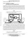
MPC8280 Architecture Overview
NOTE: Reference Documentation
The following figure replaces Figure 1-1 in the MPC8260
PowerQUICC II User’s Manual.
Figure 1-1 shows the block diagram for the MPC8280. Shaded portions are device- or
package-specific; refer to the notes that follow.
16 Kbytes
I-Cache
Freescale Semiconductor, Inc...
I-MMU
System Interface Unit
(SIU)
G2 Core
16 Kbytes
D-Cache
Bus Interface Unit
Communication Processor Module (CPM)
Timers
Interrupt
Controller
Parallel I/O
MCC2
or
Local Bus4
32 bits, up to 100 MHz
Memory Controller
32 KB
Data
RAM
Serial
DMAs
32-bit RISC Microcontroller
and Program ROM
Baud Rate
Generators
MCC11
32 KB
Instruction
RAM
PCI Bus
32 bits, up to 66 MHz
60x-to-PCI
Bridge
60x-to-Local
Bridge
D-MMU
60x Bus
Clock Counter
4 Virtual
IDMAs
IMA 1
System Functions
Microcode
FCC1
FCC2
FCC3
TC Layer Hardware1
SCC1
SCC2
SCC3
SCC4/
USB
SMC1
SMC2
SPI
I2C
Time Slot Assigner
Serial Interface
8 TDM Ports2
3 MII
Ports
2 UTOPIA
Ports3
Non-Multiplexed
I/O
Notes:
1 MPC8280 only (not on MPC8270 nor the VR package (MPC8270VR and MPC8275VR))
2 MPC8280 only (4 TDMs on MPC8270 and the VR package (MPC8270VR and MPC8275VR))
3 MPC8280 and MPC8275VR only (not on MPC8270 nor MPC8270VR)
4 No local bus on the VR package (MPC8270VR and MPC8275VR)
Figure 1-1. MPC8280 Block Diagram
MOTOROLA
Chapter 1. Overview
PRELIMINARY—SUBJECT TO CHANGE WITHOUT NOTICE
For More Information On This Product,
Go to: www.freescale.com
1-3
Freescale Semiconductor, Inc.
Freescale Semiconductor, Inc...
MPC8280 Architecture Overview
1-4
MPC8280 PowerQUICC II™ Specification
PRELIMINARY—SUBJECT TO CHANGE WITHOUT NOTICE
For More Information On This Product,
Go to: www.freescale.com
MOTOROLA
Freescale Semiconductor, Inc.
Freescale Semiconductor, Inc...
Chapter 2
Embedded MPC603e Core
The MPC8280 contains an embedded version of the MPC603e processor—the G2 core.
This processor is backward-compatible with the CPU core in previous devices in the
PowerQUICC II family. The G2 core’s major features are the same throughout the
PowerQUICC II family and are listed below; enhancements to the G2 core specific to the
MPC8280 follow.
•
•
•
High-performance, superscalar microprocessor core
— Up to three instructions issued and retired per clock
— Up to five instructions in execution per clock
— Single-cycle execution for most instructions
— Pipelined FPU for all single-precision and most double-precision operations
Five independent execution units and two register files
— BPU featuring static branch prediction
— 32-bit IU
— Fully IEEE 754-compliant FPU for both single- and double-precision operations
— LSU for data transfer between data cache and GPRs and FPRs
— SRU that executes condition register (CR), special-purpose register (SPR), and
integer add/compare instructions
— Thirty-two 32-bit GPRs for integer operands
— Thirty-two 64-bit FPRs for single- or double-precision operands
High instruction and data throughput
— Zero-cycle branch capability (branch folding)
— Programmable static branch prediction on unresolved conditional branches
— Instruction fetch unit capable of fetching two instructions per clock from the
instruction cache
— Six-entry instruction queue (IQ) that provides lookahead capability
— Independent pipelines with feed-forwarding that reduces data dependencies in
hardware
MOTOROLA
Chapter 2. Embedded MPC603e Core
PRELIMINARY—SUBJECT TO CHANGE WITHOUT NOTICE
For More Information On This Product,
Go to: www.freescale.com
2-1
Freescale Semiconductor, Inc...
Freescale Semiconductor, Inc.
•
•
•
— 16-Kbyte data cache and 16-Kbyte instruction cache
– Four-way set-associative
– Physically addressed
– LRU replacement algorithm
— Cache write-back or write-through operation programmable on a per page or per
block basis
— BPU that performs CR lookahead operations
— Address translation facilities for 4-Kbyte page size, variable block size, and
256-Mbyte segment size
— 64-entry, two-way set-associative ITLB and DTLB
— Eight-entry data and instruction BAT arrays providing 128-Kbyte to 256-Mbyte
blocks
— Software table search operations and updates supported through fast trap
mechanism
— 52-bit virtual address; 32-bit physical address
Facilities for enhanced system performance
— 32- or 64-bit split-transaction data bus interface (60x bus) with burst transfers
— Support for one-level address pipelining and out-of-order bus transactions on the
60x interface
— Hardware support for misaligned little-endian accesses
Integrated power management
— Internal processor/bus clock multiplier ratios
— Three power-saving modes: doze, nap, and sleep
— Automatic dynamic power reduction when internal functional units are idle
In-system testability and debugging features through JTAG boundary-scan
capability
Features specific to the G2 core on the MPC8280 are as follows:
•
2-2
Enhancements to the G2 core register set
— Additional HID0 bits
– Address bus enable (ABE), HID0[28]—Allows the G2 core to broadcast
dcbf, dcbi, and dcbst onto the 60x bus
– Instruction fetch enable M (IFEM), HID0[24]—Allows the G2 core to reflect
the value of the M bit during instruction translation onto the 60x bus
— HID2 register—Enables true little-endian mode, the new additional BAT
registers, and cache way locking for the G2 core.
MPC8280 PowerQUICC II™ Specification
PRELIMINARY—SUBJECT TO CHANGE WITHOUT NOTICE
For More Information On This Product,
Go to: www.freescale.com
MOTOROLA
Freescale Semiconductor, Inc.
Freescale Semiconductor, Inc...
•
•
•
•
•
— System version register (SVR)—Identifies the specific version and revision level
of the system-on-a-chip integration
— Processor version register (PVR)—Updated with a new value to identify the
version and revision level of the processor
Enhancements to cache implementation
— Instruction cache is blocked only until the critical load completes (hit under
reloads allowed)
— Minimized stalls due to load delays. The critical double word is simultaneously
written to the cache and forwarded to the requesting unit.
— HID2 register enables instruction and data cache way locking
— Optional data cache operation broadcast feature. Allows for correct system
management using an external copy-back L2 cache. Enabled by HID0[ABE].
— Cache control instructions—HID0[ABE] must be enabled to execute all cache
control instructions (icbi, dcbi, dcbf, and dcbst) excluding dcbz
Exceptions
— Hardware support for misaligned little-endian (LE) accesses. LE load/store
accesses that are not on a word boundary, with the exception of strings and
multiples, generate exceptions under the same circumstances as big-endian (BE)
accesses.
— Graphics instructions cause an alignment exception if the access is not on a word
boundary. The G2 core does not have misalignment support for eciwx and
ecowx.
— Critical interrupt exception that has higher priority than the system management
interrupt.
Bus clock—New bus multipliers are selected by the encodings of core_pll_cfg[0–4]
Instruction timing
— Integer divide instructions—divwu[o][.] and divw[o][.]—execute in 20 clock
cycles. Execution in the original MPC603e (PID6-603e) takes 37 clock cycles.
— Support for single-cycle store
— Adder/comparator added to system register unit—Allows dispatch and execution
of multiple integer add and compare instructions on each cycle.
Enhanced debug features
— Addition of three breakpoint registers—IABR2, DABR, and DABR2
— Addition of two breakpoint control registers—DBCR and IBCR
For more information on the execution units, refer to the G2 Core User’s Manual
(G2CORE/D).
MOTOROLA
Chapter 2. Embedded MPC603e Core
PRELIMINARY—SUBJECT TO CHANGE WITHOUT NOTICE
For More Information On This Product,
Go to: www.freescale.com
2-3
Freescale Semiconductor, Inc...
Freescale Semiconductor, Inc.
2-4
MPC8280 PowerQUICC II™ Specification
PRELIMINARY—SUBJECT TO CHANGE WITHOUT NOTICE
For More Information On This Product,
Go to: www.freescale.com
MOTOROLA
Freescale Semiconductor, Inc.
Freescale Semiconductor, Inc...
Chapter 3
Memory Map
The MPC8280’s internal address space is mapped within a contiguous block of memory.
This 256-Kbyte block—on the MPC8260 this block is 128 Kbytes—within the global
4-Gbyte real memory can be mapped on 256-Kbytes resolution through an
implementation-specific special register—the internal memory map register (IMMR).
Refer to Section 3.1, “Internal Memory Map Register (IMMR).”
Table 3-1 lists only registers new on the MPC8280.
NOTE: Reference Documentation
The following table supplements Table 3-1, “Internal Memory
Map,” in the MPC8260 PowerQUICC II User’s Manual.
Table 3-1. Internal Memory Map—Additional Registers
Internal Address Abbreviation
Name
Size
Section
CPM Dual-Port RAM (DPRAM)
00000–03FFF
DPRAM1
Dual-port data/BD RAM
16 Kbytes
Chapter 5
04000–07FFF
—
Reserved
16 Kbytes
—
08000–0BFFF
DPRAM2
Dual-port data/BD RAM
16 Kbytes
Chapter 5
0C000–0FFFF
—
Reserved
16 Kbytes
—
20000–27FFF
DPRAM3
Dual-port instructionRAM
32 Kbytes
Chapter 5
FCC1 Registers
1131C–1131F
FTIRRx
FCC transmit internal rate register
8 bits
8.6.5
11380
FIRPER1
FCC1 internal rate port enable register
32 bits
8.6.2
11384
FIRER1
FCC1 internal rate event register
32 bits
8.6.3
11388
FIRSR1_HI
FCC1 internal rate selection register: HI part
32 bits
8.6.4
1138C
FIRSR1_LO
FCC1 internal rate selection register: LO part
32 bits
8.6.4
11390
GFEMR1
General FCC1 expansion mode register
8 bits
8.2
FCC2 Registers
1133C–1133F
FTIRRx
FCC transmit internal rate register
8 bits
8.6.5
113A0
FIRPER2
FCC2 internal rate port enable register
32 bits
8.6.2
MOTOROLA
Chapter 3. Memory Map
PRELIMINARY—SUBJECT TO CHANGE WITHOUT NOTICE
For More Information On This Product,
Go to: www.freescale.com
3-1
Freescale Semiconductor, Inc.
Internal Memory Map Register (IMMR)
Table 3-1. Internal Memory Map—Additional Registers (continued)
Internal Address Abbreviation
Name
Size
Section
113A4
FIRER2
FCC2 internal rate event register
32 bits
8.6.3
113A8
FIRSR2_HI
FCC2 internal rate selection register: HI part
32 bits
8.6.4
113AC
FIRSR2_LO
FCC2 internal rate selection register: LO part
32 bits
8.6.4
113B0
GFEMR2
General FCC2 expansion mode register
8 bits
8.2
32 bits
8.2
FCC3 Registers
113D0
GFEMR3
General FCC3 expansion mode register
Freescale Semiconductor, Inc...
USB Registers
11B60
USMOD
USB mode register
8 bits
7.5.7.1
11B61
USADR
USB address register
8 bits
7.5.7.2
11B62
USCOM
USB command register
8 bits
7.5.7.4
11B64
USEP1
USB end point 1 register
16 bits
7.5.7.3
11B66
USEP2
USB end point 2 register
16 bits
7.5.7.3
11B68
USEP3
USB end point 3 register
16 bits
7.5.7.3
11B6A
USEP4
USB end point 4 register
16 bits
7.5.7.3
11B6C–11B6F
—
Reserved
32 bits
—
11B70
USBER
USB event register
16 bits
7.5.7.5
11B72
—
Reserved
16 bits
—
11B74
USBMR
USB mask register
16
7.5.7.6
11B77
USBS
USB status register
8 bits
7.5.7.7
11B79–11B7F
—
Reserved
56 bits
—
3.1
Internal Memory Map Register (IMMR)
NOTE: Reference Documentation
This section replaces Section 4.3.2.7, “ Internal Memory Map
Register,” in the MPC8260 PowerQUICC II User’s Manual.
The internal memory map register (IMMR), shown in Figure 3-1, contains both
identification of a specific device and the base address for the internal memory map.
Software can deduce availability and location of on-chip system resources from the values
in IMMR. Note that PARTNUM and MASKNUM are mask-programmed and cannot be
changed for any particular device.
3-2
MPC8280 PowerQUICC II™ Specification
PRELIMINARY—SUBJECT TO CHANGE WITHOUT NOTICE
For More Information On This Product,
Go to: www.freescale.com
MOTOROLA
Freescale Semiconductor, Inc.
Internal Memory Map Register (IMMR)
0
13
Field
Reset
ISB
15
—
Depends on reset configuration sequence. Refer to Section 4.3.1.1, “Hard Reset Configuration Word.”
R/W
R/W
Addr
0x101A8
16
23
Field
Freescale Semiconductor, Inc...
14
24
PARTNUM
31
MASKNUM
Reset
—
R/W
R
Addr
0x101AA
Figure 3-1. Internal Memory Map Register (IMMR)
Table 3-2 describes IMMR fields.
Table 3-2. IMMR Field Descriptions
Bits
Name
Description
0–13
ISB
Internal space base. Defines the base address of the internal memory space. The value of ISB
be configured at reset to one of 8 addresses; it can then be changed to any value by the
software. The default is 0, which maps to address 0x0000_0000.
ISB defines the 14 msbs of the memory map register base address. IMMR itself is mapped in the
internal memory space region. As soon as the ISB is written with a new base address, the IMMR
base address is relocated according to the ISB. ISB can be configured to one of 8 possible
addresses at reset to enable the configuration of multiple-MPC8280 systems.
The number of programmable bits in this field, and hence the resolution of the location of
internal space, depends on the internal memory space of a specific implementation. In the
MPC8280, all 14 bits can be programmed. See the MP8260 PowerQUICC II User’s Manual
Chapter 3, “Memory Map,” for details on the device’s internal memory map and to Chapter 5,
“Reset,” for the available default initial values.
Note: The MPC8280’s internal address space is 256 Kbytes; on the MPC8260 it is 128 Kbytes.
Also, on the MPC8280 ISB is 14 bits; on the MPC8260 it is 15 bits.
14–15
16–23
—
Reserved, should be cleared.
PARTNUM Part number. This read-only field is mask-programmed with a code corresponding to the part
number of the part on which the SIU is located. It is intended to help factory test and user code
which is sensitive to part changes. This changes when the part number changes. For example, it
would change if any new module is added or if the size of any memory module is changed. It
would not change if the part is changed to fix a bug in an existing module. The part number for
the MPC8280 is 0x0A.
24–31 MASKNUM Mask number. This read-only field is mask-programmed with a code corresponding to the mask
number of the part on which the SIU is located. It is intended to help factory test and user code
which is sensitive to part changes. It is programmed in a commonly changed layer and should
be changed for all mask set changes. The first revision of the MPC8280 has 0x00 in this field.
The value of this field is changed every revision of the device.
MOTOROLA
Chapter 3. Memory Map
PRELIMINARY—SUBJECT TO CHANGE WITHOUT NOTICE
For More Information On This Product,
Go to: www.freescale.com
3-3
Freescale Semiconductor, Inc.
Freescale Semiconductor, Inc...
Internal Memory Map Register (IMMR)
3-4
MPC8280 PowerQUICC II™ Specification
PRELIMINARY—SUBJECT TO CHANGE WITHOUT NOTICE
For More Information On This Product,
Go to: www.freescale.com
MOTOROLA
Freescale Semiconductor, Inc.
Freescale Semiconductor, Inc...
Chapter 4
PLL and Clock Generator
NOTE: Reference Documentation
This chapter replaces Chapter 9, “Clocks and Power Control,”
in the MPC8260 PowerQUICC II User’s Manual and
Section 1.3, “Clocking,” in the PCI Bridge Functional
Specification: Addendum to MPC8260 PowerQUICC II User’s
Manual.
The MPC8280’s clocking architecture includes two PLLs—the main PLL and the core
PLL. The main PLL, together with the divisors, provides the internal 60x bus clock and
internal clocks for all blocks in the chip except core blocks. The core PLL provides the
internal core clocks.
The MPC8280’s clocking is a configurable system supporting three clock configuration
modes. The clock configuration mode is set during the power on reset. Refer to Table 4-5.
CLKIN is the primary timing reference for the MPC8280. The frequency of CLKIN equals
60x and local bus frequencies. The main PLL multiplies the frequency of the input clock to
the final CPM frequency. Clock ratios for the various clock configuration modes are
presented in Section 4.6, “Clock Configuration Modes.”
4.1
MPC8280 Clock Block Diagram
The MPC8280 clocking system, shown in Figure 4-1, is designed around two PLLs—the
main PLL and the core PLL. The main PLL receives CLKIN as its input clock and
multiplies it to provide MAIN_CLK, which is twice the CPM clock, to the clock block
divisors. The divisors shown in Figure 4-1 generate all MPC8280 internal clocks by
synchronously dividing MAIN_CLK. These clocks are then output from the clock block to
the entire MPC8280.
4.1.1
Main PLL
The main PLL performs frequency multiplication and skew elimination. It allows the CPM
to operate at a high internal clock frequency while using a low-frequency clock input. This
has two immediate benefits:
MOTOROLA
Chapter 4. PLL and Clock Generator
PRELIMINARY—SUBJECT TO CHANGE WITHOUT NOTICE
For More Information On This Product,
Go to: www.freescale.com
4-1
Freescale Semiconductor, Inc.
MPC8280 Clock Block Diagram
•
•
4.1.2
A lower clock input frequency reduces overall electromagnetic interference
generated by the system
Oscillating at different frequencies eliminates the need for another oscillator
Core PLL
Freescale Semiconductor, Inc...
The core PLL has the same advantages as the main PLL; it performs frequency
multiplication and skew elimination for the core blocks. The core PLL input clock is
synchronous with the 60x bus clock. Its configuration word, CORE_PLL_CFG[0-4], is
determined by the MPC8280 clock configuration mode setting (refer to “CPU
Multiplication Factor” in Table 4-6 through Table 4-10). According to the setting, the core
PLL multiplies the internal bus clock and synchronously provides the core clocks.
4.1.3
Skew Elimination
The PLL can tighten synchronous timings by eliminating skew between phases of the
internal clock and the external clock entering the chip (CLKIN). Skew elimination is
always active when the PLL is enabled. Disabling the PLL (PLL bypass) can greatly
increase clock skew.
4.1.4
Divisors
The PLL output clock (MAIN_CLK) is twice the CPM clock. MAIN_CLK applies to
general-purpose dividers. Each MPC8280 internal clock is generated by a dedicated divisor
which is a programmable number between 1 and 16. Divisors are determined by the clock
modes presented in Section 4.6, “Clock Configuration Modes. Note that all divisors’ output
clocks will have identical skew in relation to the input clock because the delay through the
divisors for all clocks is identical independent of how it’s divisors have been programmed.
4.1.5
Internal Clock Signals
The internal logic of the MPC8280 generates the next internal clock lines:
• CPM general system clocks (CPM_CLK)
• 60x bus and local bus (BUS_CLK). Identical to CLKIN.
• SCC clocks (SCC_CLK)
• Baud-rate generator clock (BRG_CLK)
• PCI clock (PCI_CLK)
• DLL clocks
The PLL synchronizes these clock signals to each other.
4-2
MPC8280 PowerQUICC II™ Specification
PRELIMINARY—SUBJECT TO CHANGE WITHOUT NOTICE
For More Information On This Product,
Go to: www.freescale.com
MOTOROLA
Freescale Semiconductor, Inc.
MPC8280 Clock Block Diagram
MAIN PLL for CPM Clocks
CLKIN
Main PLL MF=SCMR[PLLMF]
PLL
vco out
MAIN_CLK = CLKIN * SCMR[PLLMF]
VCO
divider
=2
CPM_CLK
÷ (CPMDF + 1)
(fixed ÷2)
SCMR[CPMDF]
Freescale Semiconductor, Inc...
BUS_CLK (= CLKIN)
SCMR[BUSDF]
÷ (BUSDF + 1)
General-Purpose Divider
SCC_CLK
÷4
2*SCMR[CPMDF]
SCCR[DFBRG]
22(DFBRG + 1)
SCCR[PCIDF]
÷ (PCIDF + 1)
CORE
BRG
PCI_CLK
Note: Used in
PCI modes only
CORE PLL
PLL
SCMR[CORECNF]
CORE_CLK
vco
BUS_CLK
VCO
divider
VCO_DF
Notes:
1 In PCI agent mode CLKIN is the PCI clock (input to MPC8280).
2 SCMR register is read only register. Its value is determined during Poweron Reset. Refer to Section 4.5, “System
Clock Mode Register (SCMR)."
Figure 4-1. MPC8280 System Clock Architecture
MOTOROLA
Chapter 4. PLL and Clock Generator
PRELIMINARY—SUBJECT TO CHANGE WITHOUT NOTICE
For More Information On This Product,
Go to: www.freescale.com
4-3
Freescale Semiconductor, Inc.
MPC8280 Clock Block Diagram
4.1.6
PCI Bridge as an Agent
Operating from the PCI System Clock
Freescale Semiconductor, Inc...
If the MPC8280 is connected to a system which generates the PCI clock, the PCI clock
should be fed to the CLKIN1 pin. The PCI clock is internally multiplied by the PLL to
generate the chip’s internal high speed clock. This clock is used to generate the 60x bus
clock (refer to Table 4-9 and Table 4-10.) The 60x bus clock is then driven by a DLL circuit
to the DLLOUT pin, which has a feedback path from the board to the CLKIN2 pin. This
feedback clock signal is used by the DLL logic to minimize clock skew between the internal
and external clocks.
NOTE
All PCI timings are measured relative to CLKIN1; all 60x bus
timings are measured relative to CLKIN2.
CPM_CLK
MPC8280
PCI Interface
PCI_CLK
%
Dividers
%
BUS_CLK
dllout
PCI Circuit
60x Circuit
PLL
DLL
BUS_CLK
clkin2
Bus Clock
clkin1
PCI Clock
Figure 4-2. PCI Bridge as an Agent, Operating from the PCI System Clock
4.1.7
PCI Bridge as a Host Generating the PCI System Clock
In a system where the MPC8280 is the host that generates the PCI clock, the 60x bus clock
should be driven to the CLKIN1 pin. The 60x bus clock is internally multiplied by the PLL
to generate the CPM high speed clock and then internally divided to generate the PCI bus
clock. The PCI bus clock is then driven by the DLL circuit to the DLLOUT pin, which has
a feedback path from the board to the CLKIN2 pin. This feedback controls clock skew by
ensuring the same internal and external clock timing.
NOTE
All PCI timings are measured relative to CLKIN2, and all 60x
bus timings are measured relative to CLKIN1.
4-4
MPC8280 PowerQUICC II™ Specification
PRELIMINARY—SUBJECT TO CHANGE WITHOUT NOTICE
For More Information On This Product,
Go to: www.freescale.com
MOTOROLA
Freescale Semiconductor, Inc.
CPM_CLK
External Clock Inputs
MPC8280
PCI Interface
PCI_CLK
%
Dividers
%
BUS_CLK
60x Circuit
dllout
PCI Circuit
PLL
DLL
PCI_CLK
Freescale Semiconductor, Inc...
clkin2
clkin1
60x Bus Clock
PCI Clock
Figure 4-3. PCI Bridge as a Host, Generating the PCI System Clock
4.2
External Clock Inputs
The input clock source to the PLL is an external clock oscillator at the bus frequency. The
PLL skew elimination between the CLOCKIN pin and the internal bus clock is guaranteed.
4.3
PLL Pins
Table 4-1 shows the dedicated PLL pins.
Table 4-1. Dedicated PLL Pins
Signal
Description
VCCSYN1 Drain Voltage—Analog VDD dedicated to core analog PLL circuits. To ensure core clock stability, filter the
power to the VCCSYN1 input with a circuit similar to the one in "PLL Filtering Curcuit" Figure. To filter as
much noise as possible, place the circuit as close as possible to VCCSYN1. The 0.1-µF capacitor should
be closest to VCCSYN1, followed by the 10-µF capacitor, and finally the 10-Ω resistor to Vdd. These
traces should be kept short and direct.
VCCSYN Drain Voltage—Analog VDD dedicated to analog main PLL circuits. To ensure internal clock stability, filter
the power to the VCCSYN input with a circuit similar to the one in "PLL Filtering Curcuit" Figure. To filter
as much noise as possible, place the circuit should as close as possible to VCCSYN. The 0.1-µF
capacitor should be closest to VCCSYN, followed by the 10-µF capacitor, and finally the 10-Ω resistor to
Vdd. These traces should be kept short and direct.
MOTOROLA
Chapter 4. PLL and Clock Generator
PRELIMINARY—SUBJECT TO CHANGE WITHOUT NOTICE
For More Information On This Product,
Go to: www.freescale.com
4-5
Freescale Semiconductor, Inc.
PLL Pins
10ohm
VDD
VCCSYN
0.1uF
10uF
Figure 4-4. PLL Filtering Circuit
Freescale Semiconductor, Inc...
4.3.1
Important Differences: MPC8280 vs. MPC826x(A)
4.3.1.1
Hard Reset Configuration Word
NOTE: Reference Documentation
This section replaces Section 5.4.1, “Hard Reset Configuration
Word,” in the MPC8260 PowerQUICC II User’s Manual. Note
the addition of bit 12 (PLLBP); this is the only change.
The contents of the hard reset configuration word are shown in Figure 4-5.
0
1
2
3
Field EARB EXMC CDIS EBM
4
5
BPS
Reset
6
7
CIP
ISPS
8
9
L2CPC
10
11
DPPC
12
13
PLLBP
15
ISB
0000_0000_0000_0000
16
Field BMS
17
BBD
Reset
18
19
MMR
20
21
LBPC
22
23
APPC
24
25
CS10PC
26
27
ALD_EN
—
28
31
MODCK_H
0000_0000_0000_0000
Figure 4-5. Hard Reset Configuration Word
Table 4-2 describes hard reset configuration word fields.
Table 4-2. Hard Reset Configuration Word Field Descriptions
Bits
Name
Description
0
EARB 1
External arbitration. Defines the initial value for ACR[EARB]. If EARB = 1, external arbitration is
assumed. See Section 4.3.2.2, “60x Bus Arbiter Configuration Register (PPC_ACR),” in the
MPC8260 PowerQUICC II User’s Manual.
1
EXMC
External MEMC. Defines the initial value of BR0[EMEMC]. If EXMC = 1, an external memory
controller is assumed. See Section 10.3.1, “Base Registers (BRx),” in the MPC8260
PowerQUICC II User’s Manual.
2
CDIS1
Core disable. Defines the initial value for the SIUMCR[CDIS].
0 The core is active. See Section 4.3.2.6, “SIU Module Configuration Register (SIUMCR),” in
the MPC8260 PowerQUICC II User’s Manual.
1 The core is disabled. In this mode the MPC8280 functions as a slave.
4-6
MPC8280 PowerQUICC II™ Specification
PRELIMINARY—SUBJECT TO CHANGE WITHOUT NOTICE
For More Information On This Product,
Go to: www.freescale.com
MOTOROLA
Freescale Semiconductor, Inc.
PLL Pins
Freescale Semiconductor, Inc...
Table 4-2. Hard Reset Configuration Word Field Descriptions (continued)
Bits
Name
3
EBM1
4–5
BPS
Boot port size. Defines the initial value of BR0[PS], the port size for memory controller bank 0.
00 64-bit port size
01 8-bit port size
10 16-bit port size
11 32-bit port size
See Section 10.3.1, “Base Registers (BRx),” in the MPC8260 PowerQUICC II User’s Manual.
6
CIP1
Core initial prefix. Defines the initial value of MSR[IP]. Exception prefix. The setting of this bit
specifies whether an exception vector offset is prepended with Fs or 0s. In the following
description, nnnnn is the offset of the exception vector.
0 MSR[IP] = 1 (default). Exceptions are vectored to the physical address 0xFFFn_nnnn
1 MSR[IP] = 0 Exceptions are vectored to the physical address 0x000n_nnnn.
7
ISPS1
Internal space port size. Defines the initial value of BCR[ISPS]. Setting ISPS configures the
MPC8260 to respond to accesses from a 32-bit external master to its internal space. See
Section 4.3.2.1, “Bus Configuration Register (BCR),” in the MPC8260 PowerQUICC II User’s
Manual.
8–9
L2CPC1
L2 cache pins configuration. Defines the initial value of SIUMCR[L2CPC]. See Section 4.3.2.6,
“SIU Module Configuration Register (SIUMCR),” in the MPC8260 PowerQUICC II User’s Manual.
10–11
DPPC1
Data parity pin configuration. Defines the initial value of SIUMCR[DPPC]. For more details refer
to Section 4.3.2.6, “SIU Module Configuration Register (SIUMCR),” in the MPC8260
PowerQUICC II User’s Manual.
12
PLLBP
PLL bypass
0 Normal operation
1 Bypass CPM PLL
13–15
ISB
Initial internal space base select. Defines the initial value of IMMR[0–14] and determines the
base address of the internal memory space.
000 0x0000_0000
001 0x00F0_0000
010 0x0F00_0000
011 0x0FF0_0000
100 0xF000_0000
101 0xF0F0_0000
110 0xFF00_0000
111 0xFFF0_0000
See Section 4.3.2.7, “Internal Memory Map Register (IMMR),” in the MPC8260 PowerQUICC II
User’s Manual.
16
BMS
Boot memory space. Defines the initial value for BR0[BA]. There are two possible boot memory
regions: HIMEM and LOMEM.
0 0xFE00_0000—0xFFFF_FFFF
1 0x0000_0000—0x01FF_FFFF
See Section 10.3.1, “Base Registers (BRx).”
17
BBD
Bus busy disable. Defines the initial value of SIUMCR[BBD]. See Section 4.3.2.6, “SIU Module
Configuration Register (SIUMCR),” in the MPC8260 PowerQUICC II User’s Manual.
18–19
MMR
Mask masters requests. Defines the initial value of SIUMCR[MMR]. See Section 4.3.2.6, “SIU
Module Configuration Register (SIUMCR),” in the MPC8260 PowerQUICC II User’s Manual.
MOTOROLA
Description
External bus mode. Defines the initial value of BCR[EBM]. See Section 4.3.2.1, “Bus
Configuration Register (BCR),” in the MPC8260 PowerQUICC II User’s Manual.
Chapter 4. PLL and Clock Generator
PRELIMINARY—SUBJECT TO CHANGE WITHOUT NOTICE
For More Information On This Product,
Go to: www.freescale.com
4-7
Freescale Semiconductor, Inc.
PLL Pins
Table 4-2. Hard Reset Configuration Word Field Descriptions (continued)
Bits
Name
20–21
LBPC1
Description
Local bus pin configuration. Defines the value of SIUMCR[LBPC]. See Section 4.3.2.6, “SIU
Module Configuration Register (SIUMCR).”
Freescale Semiconductor, Inc...
00 Local bus pins function as local bus
01 Local bus pins function as PCI bus.
10 Local bus pins function as core pins
11 Reserved
22–23
APPC1
Address parity pin configuration. Defines the initial value of SIUMCR[APPC]. See
Section 4.3.2.6, “SIU Module Configuration Register (SIUMCR),” in the MPC8260 PowerQUICC
II User’s Manual.
24–25
CS10PC1
CS10 pin configuration. Defines the initial value of SIUMCR[CS10PC]. See Section 4.3.2.6, “SIU
Module Configuration Register (SIUMCR),” in the MPC8260 PowerQUICC II User’s Manual.
26
ALD_EN
27
—
CP auto load enable. Allows the CP to automatically load the essential PCI configuration
registers from the EEPROM during reset.
0 CP auto load is disabled.
1 CP auto load is enabled.
Reserved, should be cleared.
28–31 MODCK_H High-order bits of the MODCK bus, which determine the clock reset configuration. (If the device
is configured to PCI mode (PCI_MODE is driven low), this field has no effect and the value for
MODCK_H is loaded directly from the MODCK_H pins.
Note: The value of the MODCK_H bits are derived from the dedicated PCI_MODCK_H[0–3]
pins when operating in PCI mode.
1
This bit cannot be changed after reset.
4.3.1.2
External Filter Capacitor (XFC)
The XFC pin that is used in the MPC826x(A) is not used in the MPC8280. There is no need
for external capacitor to operate the PLL. New designs should connect AB2 (XFC) pin to
GND. Old designs (when the MPC8280 is used as a drop-in replacement) can leave the pin
connected to the current capacitor.
4.3.1.3
GNDSYN
GNDSYN exists on the MPC826x(A) but does not exist as a separate ground signal in the
MPC8280. New designs must connect AB1 pin to GND and follow layout practices
suggested in the MPC8280 Hardware Specifications. Old designs (when the MPC8280 is
used as a drop-in replacement) can leave the pin connected to GND with the noise filtering
capacitors.
4-8
MPC8280 PowerQUICC II™ Specification
PRELIMINARY—SUBJECT TO CHANGE WITHOUT NOTICE
For More Information On This Product,
Go to: www.freescale.com
MOTOROLA
Freescale Semiconductor, Inc.
System Clock Control Register (SCCR)
4.4
System Clock Control Register (SCCR)
The system clock control register (SCCR), shown in Figure 4-6, is memory-mapped into
the MPC8280’s internal space.
0
22
Field
—
Reset
0
23
24
25
28
PCI_MODE PCI_MODCK
PCIDF
Refer to Table 4-3
R/W
R
Addr
0x10C80
29
30
31
CLPD
DFBRG
0
01
Freescale Semiconductor, Inc...
Figure 4-6. System Clock Control Register (SCCR)
Table 4-3 SCCR Field Descriptions describes SCCR fields.
Table 4-3. SCCR Field Descriptions
Defaults
Bits
Name
Description
POR
0–22 —
Hard Reset
0
Unaffected
Reserved
PCI_Mode
Unaffected
PCI Mode
0 Disabled
1 Enabled
Reflects the inverted value of the PCI_Mode pin.
23
PCI_MODE
24
PCI_MODCK PCI_MODCK Unaffected
25–28 PCIDF
29
CLPD
30–31 DFBRG
MOTOROLA
Reflects the value of the PCI_MODCK pin.
Config pins
Unaffected
PCI division factor.
0
Unaffected
CPM low power disable.
0 Default. CPM does not enter low power mode when the core
enters low power mode.
1 CPM and SIU enter low power mode when the core does. This
may be useful for debug tools that use the assertion of QREQ
as an indication of breakpoint in the core.
01
Unaffected
Division factor of BRGCLK. Defines the BRGCLK frequency.
Changing the value does not result in a loss of lock condition.
The BRGCLK is divided from the CPM clock.
00 Divide by 2
01 Divide by 8 (normal operation)
10 Divide by 32
11 Divide by 128
Chapter 4. PLL and Clock Generator
PRELIMINARY—SUBJECT TO CHANGE WITHOUT NOTICE
For More Information On This Product,
Go to: www.freescale.com
4-9
Freescale Semiconductor, Inc.
System Clock Mode Register (SCMR)
4.5
System Clock Mode Register (SCMR)
The PLL, low power, and reset control register (SCMR), shown in Figure 4-7, hold the
parameters necessary for determining the output clock frequencies. To understand how the
interaction of these values, refer to Section 4.1, “MPC8280 Clock Block Diagram.”
Freescale Semiconductor, Inc...
0
2
Field
—
Reset
000
3
7
8
CORECNF
11
12
BUSDF
15
CPMDF
Refer to Table 4-4
R/W
R
Addr
0x10C88
16
27
28
31
Field
—
PLLMF
Reset
0000_0000_0000
Refer to Table 4-4
R/W
R
Addr
0x10C8A
Figure 4-7. System Clock Mode Register (SCMR)
Table 4-4 describes SCMR fields.
Table 4-4. SCMR Field Descriptions
Defaults
Bits
0–2
3–7
Name
—
Description
POR
Hard Reset
—
—
CORECNF Config pins
Reserved
Unaffected Core PLL configuration.
8–11
BUSDF
Config pins
Unaffected 60x bus division factor.
12–15
CPMDF
Config pins
Unaffected CPM division factor. This value is always 1.
16–27
—
—
28–31
PLLMF
Config pins
4-10
—
Reserved
Unaffected PLLMF control the value of the divider in the PLL feedback loop.
MPC8280 PowerQUICC II™ Specification
PRELIMINARY—SUBJECT TO CHANGE WITHOUT NOTICE
For More Information On This Product,
Go to: www.freescale.com
MOTOROLA
Freescale Semiconductor, Inc.
Clock Configuration Modes
4.6
Clock Configuration Modes
The MPC8280 has three clocking modes: local, PCI host, and PCI agent. The clocking
mode is set according to three input pins—PCI_MODE, PCI_CFG[0], PCI_MODCK—as
shown in Table 4-5.
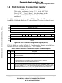
Table 4-5. MPC8280 Clocking Modes
Pins
Freescale Semiconductor, Inc...
PCI Clock
Frequency Range
(MHZ)
Reference
PCI_CFG[0] PCI_MODCK 1
PCI_MODE
1
Clocking Mode
1
—
—
Local bus
—
Table 4-6
0
0
0
PCI host
50–66
Table 4-7
0
0
1
25–50
Table 4-8
0
1
0
50–66
Table 4-9
0
1
1
25–50
Table 4-10
PCI agent
Determines PCI clock frequency range. Refer to Section 4.6.2, “PCI Mode.”
In each clocking mode, the configuration of bus, core, PCI, and CPM frequencies is
determined by seven bits during the power-up reset—three hardware configuration pins
(MODCK[1–3]) and four bits from hardware configuration word[28–31] (MODCK_H).
Both the PLLs and the dividers are set according to the selected MPC8280 clock operation
mode as described in the following sections.
4.6.1
Local Bus Mode
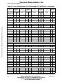
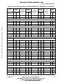
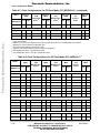
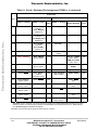
Table 4-6 lists default and full configurations for the MPC8280 in local bus mode.
NOTE
Clock configuration is set while POR is asserted.
Table 4-6. Local Bus Clock Modes
Bus Clock 2, 3
(MHz)
Mode 1
MODCK_H-MODCK[1-3]
low
high
CPM
Multiplication
Factor 4
CPM Clock3
(MHz)
low
high
CPU
Multiplication
Factor 5
CPU Clock3
(MHz)
low
high
Default Modes (MODCK_H= 0000)
0000_000
62.5
133.3
3
187.5
400.0
4
250.0
533.3
0000_001
50.0
133.3
3
150.0
400.0
5
250.0
666.7
0000_010
62.5
100.0
4
250.0
400.0
4
250.0
400.0
0000_011
50.0
100.0
4
200.0
400.0
5
250.0
500.0
0000_100
50.0
167.0
2
100.0
334.0
2.5
125.0
417.5
0000_101
50.0
167.0
2
100.0
334.0
3
150.0
501.0
MOTOROLA
Chapter 4. PLL and Clock Generator
PRELIMINARY—SUBJECT TO CHANGE WITHOUT NOTICE
For More Information On This Product,
Go to: www.freescale.com
4-11
Freescale Semiconductor, Inc.
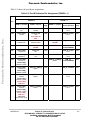
Clock Configuration Modes
Table 4-6. Local Bus Clock Modes (continued)
Bus Clock 2, 3
(MHz)
Mode 1
MODCK_H-MODCK[1-3]
low
high
0000_110
50.0
160.0
0000_111
41.7
160.0
CPM
Multiplication
Factor 4
CPM Clock3
(MHz)
low
high
2.5
125.0
400.0
2.5
104.2
CPU
Multiplication
Factor 5
CPU Clock3
(MHz)
low
high
2.5
125.0
400.0
400.0
3
125.0
480.0
Freescale Semiconductor, Inc...
Full Configuration Modes
0001_000
62.5
167.0
2
125.0
334.0
4
250.0
668.0
0001_001
50.0
167.0
2
100.0
334.0
5
250.0
835.0
0001_010
50.0
167.0
2
100.0
334.0
6
300.0
1002.0
0001_011
Reserved
0001_100
Reserved
0001_101
62.5
133.3
3
187.5
400.0
4
250.0
533.3
0001_110
50.0
133.3
3
150.0
400.0
5
250.0
666.7
1000_111
45.5
133.3
3
136.4
400.0
5.5
250.0
733.3
0001_111
41.7
133.3
3
125.0
400.0
6
250.0
800.0
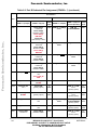
0010_000
Reserved
0010_001
Reserved
0010_010
62.5
100.0
4
250.0
400.0
4
250.0
400.0
0010_011
50.0
100.0
4
200.0
400.0
5
250.0
500.0
0010_100
41.7
100.0
4
166.7
400.0
6
250.0
600.0
0010_101
35.7
100.0
4
142.9
400.0
7
250.0
700.0
0010_110
31.3
100.0
4
125.0
400.0
8
250.0
800.0
0010_111
4-12
Reserved
0011_000
50.0
80.0
5
250.0
400.0
5
250.0
400.0
0011_001
41.7
80.0
5
208.3
400.0
6
250.0
480.0
0011_010
35.7
80.0
5
178.6
400.0
7
250.0
560.0
0011_011
31.3
80.0
5
156.3
400.0
8
250.0
640.0
0011_100
Reserved
0011_101
Reserved
0011_110
41.7
66.7
6
250.0
400.0
6
250.0
400.0
0011_111
35.7
66.7
6
214.3
400.0
7
250.0
466.7
0100_000
31.3
66.7
6
187.5
400.0
8
250.0
533.3
MPC8280 PowerQUICC II™ Specification
PRELIMINARY—SUBJECT TO CHANGE WITHOUT NOTICE
For More Information On This Product,
Go to: www.freescale.com
MOTOROLA
Freescale Semiconductor, Inc.
Clock Configuration Modes
Table 4-6. Local Bus Clock Modes (continued)
Bus Clock 2, 3
(MHz)
Freescale Semiconductor, Inc...
Mode 1
MODCK_H-MODCK[1-3]
low
high
0101_101
62.5
167.0
0101_110
50.0
0101_111
CPM
Multiplication
Factor 4
CPM Clock3
(MHz)
low
high
2
125.0
334.0
167.0
2
100.0
50.0
167.0
2
0110_000
71.4
167.0
0110_001
62.5
0110_010
55.6
CPU
Multiplication
Factor 5
CPU Clock3
(MHz)
low
high
2
125.0
334.0
334.0
2.5
125.0
417.5
100.0
334.0
3
150.0
501.0
2
142.9
334.0
3.5
250.0
584.5
167.0
2
125.0
334.0
4
250.0
668.0
167.0
2
111.1
334.0
4.5
250.0
751.5
0110_011
Reserved
0110_100
50.0
160.0
2.5
125.0
400.0
2.5
125.0
400.0
0110_101
41.7
160.0
2.5
104.2
400.0
3
125.0
480.0
0110_110
71.4
160.0
2.5
178.6
400.0
3.5
250.0
560.0
0110_111
62.5
160.0
2.5
156.3
400.0
4
250.0
640.0
0111_000
55.6
160.0
2.5
138.9
400.0
4.5
250.0
720.0
0111_001
Reserved
0111_010
Reserved
0111_011
41.7
133.3
3
125.0
400.0
3
125.0
400.0
0111_100
71.4
133.3
3
214.3
400.0
3.5
250.0
466.7
0111_101
62.5
133.3
3
187.5
400.0
4
250.0
533.3
0111_110
55.6
133.3
3
166.7
400.0
4.5
250.0
600.0
0111_111
Reserved
1000_000
Reserved
1000_001
Reserved
1000_010
71.4
114.3
3.5
250.0
400.0
3.5
250.0
400.0
1000_011
62.5
114.3
3.5
218.8
400.0
4
250.0
457.1
1000_100
55.6
114.3
3.5
194.4
400.0
4.5
250.0
514.3
1000_101
50.0
114.3
3.5
175.0
400.0
5
250.0
571.4
1000_110
45.5
114.3
3.5
159.1
400.0
5.5
250.0
628.6
1100_000
50.0
167.0
2
100.0
334.0
Bypass
50.0
167.0
MOTOROLA
Chapter 4. PLL and Clock Generator
PRELIMINARY—SUBJECT TO CHANGE WITHOUT NOTICE
For More Information On This Product,
Go to: www.freescale.com
4-13
Freescale Semiconductor, Inc.
Clock Configuration Modes
Table 4-6. Local Bus Clock Modes (continued)
Bus Clock 2, 3
(MHz)
Mode 1
MODCK_H-MODCK[1-3]
low
high
1100_001
40.0
160.0
1100_010
33.3
133.3
1101_000
1
2
Freescale Semiconductor, Inc...
3
4
5
CPM
Multiplication
Factor 4
CPM Clock3
(MHz)
low
high
2.5
100.0
400.0
3
100.0
400.0
CPU
Multiplication
Factor 5
CPU Clock3
(MHz)
low
high
Bypass
40.0
160.0
Bypass
33.3
133.3
Reserved
MODCK_H = hard reset configuration word [28–31]. Refer to Section 5.4 in the MPC8260 User’s Manual;
MODCK[1-3] = three hardware configuration pins.
60x and local bus frequency. Identical to CLKIN.
‘High’ and ‘low’ indicate frequency limits for a given configuration.
CPM multiplication factor = CPM clock/bus clock
CPU multiplication factor = Core PLL multiplication factor
4.6.2
PCI Mode
The following tables show the possible clock configurations for the MPC8280 in both PCI
host and PCI agent modes. In addition, note the following:
NOTE
In PCI mode only, PCI_MODCK comes from the LGPL5 pin
and MODCK_H[0–3] comes from {LGPL0, LGPL1, LGPL2,
LGPL3}.
NOTE
The minimum Tval = 2 when PCI_MODCK = 1 and minimum
Tval = 1 when PCI_MODCK = 0; therefore, board designers
should use clock configurations that fit this condition to achieve
PCI-compliant AC timing.
4.6.2.1
PCI Host Mode
Table 4-7 and Table 4-8 show configurations for PCI host mode. Note that the range of the
PCI clock frequency is determined by PCI_MODCK.
4-14
MPC8280 PowerQUICC II™ Specification
PRELIMINARY—SUBJECT TO CHANGE WITHOUT NOTICE
For More Information On This Product,
Go to: www.freescale.com
MOTOROLA
Freescale Semiconductor, Inc.
Clock Configuration Modes
Table 4-7. Clock Configurations for PCI Host Mode (PCI_MODCK=0) 1
Mode 2
MODCK_HMODCK[1-3]
Bus Clock 3, 4
(MHz)
low
high
CPM
Multiplication
Factor 5
CPM Clock4
(MHz)
low
high
CPU
Multiplication
Factor 6
CPU Clock4
(MHz)
low
high
PCI
Division
Factor
PCI Clock
(MHz)
low high
Freescale Semiconductor, Inc...
Default Modes (MODCK_H=0000)
0000_000
50.0
66.7
2
100.0 133.3
2.5
125.0 166.7
2
50.0 66.7
0000_001
50.0
66.7
2
100.0 133.3
3
150.0 200.0
2
50.0 66.7
0000_010
60.0
80.0
2.5
150.0 200.0
3
180.0 240.0
3
50.0 66.7
0000_011
71.4
80.0
2.5
178.6 200.0
3.5
250.0 280.0
3
59.5 66.7
0000_100
62.5
80.0
2.5
156.3 200.0
4
250.0 320.0
3
52.1 66.7
0000_101
50.0
66.7
3
150.0 200.0
3
150.0 200.0
3
50.0 66.7
250.0 266.6
3
62.5 66.7
0000_110
0000_111
PCI host mode (PCI_MODCK=1) only (refer to Table 4-8)
62.5
66.7
3
187.5 200.0
4
Full Configuration Modes
0001_000
50.0
66.7
3
150.0 200.0
5
250.0 333.3
3
50.0 66.7
0001_001
50.0
66.7
3
150.0 200.0
6
300.0 400.0
3
50.0 66.7
0001_010
50.0
66.7
3
150.0 200.0
7
350.0 466.6
3
50.0 66.7
0001_011
50.0
66.7
3
150.0 200.0
8
400.0 533.3
3
50.0 66.7
0010_000
50.0
66.7
4
200.0 266.6
5
250.0 333.3
4
50.0 66.7
0010_001
50.0
66.7
4
200.0 266.6
6
300.0 400.0
4
50.0 66.7
0010_010
50.0
66.7
4
200.0 266.6
7
350.0 466.6
4
50.0 66.7
0010_011
50.0
66.7
4
200.0 266.6
8
400.0 533.3
4
50.0 66.7
0010_100
75.0 100.0
4
300.0 400.0
5
375.0 500.0
6
50.0 66.7
0010_101
75.0 100.0
4
300.0 400.0
5.5
412.5 549.9
6
50.0 66.7
0010_110
75.0 100.0
4
300.0 400.0
6
450.0 599.9
6
50.0 66.7
0011_000
50.0
66.7
5
250.0 333.3
5
250.0 333.3
5
50.0 66.7
0011_001
50.0
66.7
5
250.0 333.3
6
300.0 400.0
5
50.0 66.7
0011_010
50.0
66.7
5
250.0 333.3
7
350.0 466.6
5
50.0 66.7
0011_011
50.0
66.7
5
250.0 333.3
8
400.0 533.3
5
50.0 66.7
0100_000
Reserved
0100_001
50.0
66.7
6
300.0 400.0
6
300.0 400.0
6
50.0 66.7
0100_010
50.0
66.7
6
300.0 400.0
7
350.0 466.6
6
50.0 66.7
MOTOROLA
Chapter 4. PLL and Clock Generator
PRELIMINARY—SUBJECT TO CHANGE WITHOUT NOTICE
For More Information On This Product,
Go to: www.freescale.com
4-15
Freescale Semiconductor, Inc.
Clock Configuration Modes
Table 4-7. Clock Configurations for PCI Host Mode (PCI_MODCK=0) 1 (continued)
Mode 2
Bus Clock 3, 4
(MHz)
CPM
Multiplication
Factor 5
CPU
Multiplication
Factor 6
CPU Clock4
(MHz)
PCI
Division
Factor
PCI Clock
(MHz)
MODCK_HMODCK[1-3]
low
high
0100_011
50.0
66.7
6
300.0 400.0
8
400.0 533.3
6
50.0 66.7
0101_000
50.0
66.7
2
100.0 133.3
2.5
125.0 166.7
2
50.0 66.7
0101_001
50.0
66.7
2
100.0 133.3
3
150.0 200.0
2
50.0 66.7
0101_010
Freescale Semiconductor, Inc...
CPM Clock4
(MHz)
low
high
low
high
low high
PCI host mode (PCI_MODCK=1) only (refer to Table 4-8)
0101_011
62.5
66.7
2
125.0 133.3
4
250.0 266.6
2
62.5 66.7
0101_100
55.6
66.7
2
111.1 133.3
4.5
250.0 300.0
2
55.6 66.7
0110_000
60.0
80.0
2.5
150.0 200.0
2.5
150.0 200.0
3
50.0 66.7
0110_001
60.0
80.0
2.5
150.0 200.0
3
180.0 240.0
3
50.0 66.7
0110_010
71.4
80.0
2.5
178.6 200.0
3.5
250.0 280.0
3
59.5 66.7
0110_011
62.5
80.0
2.5
156.3 200.0
4
250.0 320.0
3
52.1 66.7
0110_100
60.0
80.0
2.5
150.0 200.0
4.5
270.0 360.0
3
50.0 66.7
0110_101
60.0
80.0
2.5
150.0 200.0
5
300.0 400.0
3
50.0 66.7
0110_110
60.0
80.0
2.5
150.0 200.0
6
360.0 480.0
3
50.0 66.7
150.0 200.0
3
50.0 66.7
0111_000
0111_001
Reserved
50.0
66.7
3
0111_010
150.0 200.0
3
PCI host mode (PCI_MODCK=1) only (refer to Table 4-8)
0111_011
62.5
66.7
3
187.5 200.0
4
250.0 266.6
3
62.5 66.7
0111_100
55.6
66.7
3
166.7 200.0
4.5
250.0 300.0
3
55.6 66.7
1000_000
Reserved
1000_001
66.7
88.9
3
200.0 266.6
3
200.0 266.6
4
50.0 66.7
1000_010
71.4
88.9
3
214.3 266.6
3.5
250.0 311.1
4
53.6 66.7
1000_011
66.7
88.9
3
200.0 266.6
4
266.7 355.5
4
50.0 66.7
1000_100
66.7
88.9
3
200.0 266.6
4.5
300.0 400.0
4
50.0 66.7
1000_101
66.7
88.9
3
200.0 266.6
6
400.0 533.3
4
50.0 66.7
1000_110
66.7
88.9
3
200.0 266.6
6.5
433.3 577.7
4
50.0 66.7
1001_000
57.1
76.2
3.5
200.0 266.6
2.5
142.9 190.5
4
50.0 66.7
1001_001
57.1
76.2
3.5
200.0 266.6
3
171.4 228.5
4
50.0 66.7
1001_010
71.4
76.2
3.5
250.0 266.6
3.5
250.0 266.6
4
62.5 66.7
4-16
MPC8280 PowerQUICC II™ Specification
PRELIMINARY—SUBJECT TO CHANGE WITHOUT NOTICE
For More Information On This Product,
Go to: www.freescale.com
MOTOROLA
Freescale Semiconductor, Inc.
Clock Configuration Modes
Table 4-7. Clock Configurations for PCI Host Mode (PCI_MODCK=0) 1 (continued)
Freescale Semiconductor, Inc...
Mode 2
Bus Clock 3, 4
(MHz)
CPM
Multiplication
Factor 5
CPM Clock4
(MHz)
CPU
Multiplication
Factor 6
CPU Clock4
(MHz)
PCI
Division
Factor
PCI Clock
(MHz)
MODCK_HMODCK[1-3]
low
high
1001_011
62.5
76.2
3.5
218.8 266.6
4
250.0 304.7
4
54.7 66.7
1001_100
57.1
76.2
3.5
200.0 266.6
4.5
257.1 342.8
4
50.0 66.7
1001_101
85.7 114.3
3.5
300.0 400.0
5
428.6 571.4
6
50.0 66.7
1001_110
85.7 114.3
3.5
300.0 400.0
5.5
471.4 628.5
6
50.0 66.7
1001_111
85.7 114.3
3.5
300.0 400.0
6
514.3 685.6
6
50.0 66.7
1010_000
75.0 100.0
2
150.0 200.0
2
150.0 200.0
3
50.0 66.7
1010_001
75.0 100.0
2
150.0 200.0
2.5
187.5 250.0
3
50.0 66.7
1010_010
75.0 100.0
2
150.0 200.0
3
225.0 300.0
3
50.0 66.7
1010_011
75.0 100.0
2
150.0 200.0
3.5
262.5 350.0
3
50.0 66.7
1010_100
75.0 100.0
2
150.0 200.0
4
300.0 400.0
3
50.0 66.7
low
high
1011_000
low
high
low high
Reserved
1011_001
80.0 106.7
2.5
200.0 266.6
2.5
200.0 266.6
4
50.0 66.7
1011_010
80.0 106.7
2.5
200.0 266.6
3
240.0 320.0
4
50.0 66.7
1011_011
80.0 106.7
2.5
200.0 266.6
3.5
280.0 373.3
4
50.0 66.7
1011_100
80.0 106.7
2.5
200.0 266.6
4
320.0 426.6
4
50.0 66.7
1011_101
80.0 106.7
2.5
200.0 266.6
4.5
360.0 480.0
4
50.0 66.7
1101_000
100.0 133.3
2.5
250.0 333.3
3
300.0 400.0
5
50.0 66.7
1101_001
100.0 133.3
2.5
250.0 333.3
3.5
350.0 466.6
5
50.0 66.7
1101_010
100.0 133.3
2.5
250.0 333.3
4
400.0 533.3
5
50.0 66.7
1101_011
100.0 133.3
2.5
250.0 333.3
4.5
450.0 599.9
5
50.0 66.7
1101_100
100.0 133.3
2.5
250.0 333.3
5
500.0 666.6
5
50.0 66.7
1101_101
125.0 166.7
2
250.0 333.3
3
375.0 500.0
5
50.0 66.7
1101_110
125.0 166.7
2
250.0 333.3
4
500.0 666.6
5
50.0 66.7
1110_000
100.0 133.3
3
300.0 400.0
3.5
350.0 466.6
6
50.0 66.7
1110_001
100.0 133.3
3
300.0 400.0
4
400.0 533.3
6
50.0 66.7
1110_010
100.0 133.3
3
300.0 400.0
4.5
450.0 599.9
6
50.0 66.7
1110_011
100.0 133.3
3
300.0 400.0
5
500.0 666.6
6
50.0 66.7
MOTOROLA
Chapter 4. PLL and Clock Generator
PRELIMINARY—SUBJECT TO CHANGE WITHOUT NOTICE
For More Information On This Product,
Go to: www.freescale.com
4-17
Freescale Semiconductor, Inc.
Clock Configuration Modes
Table 4-7. Clock Configurations for PCI Host Mode (PCI_MODCK=0) 1 (continued)
Mode 2
MODCK_HMODCK[1-3]
Freescale Semiconductor, Inc...
1
2
3
4
5
6
Bus Clock 3, 4
(MHz)
low
high
CPM
Multiplication
Factor 5
CPM Clock4
(MHz)
low
high
CPU
Multiplication
Factor 6
1110_100
100.0 133.3
3
300.0 400.0
5.5
1100_000
50.0
66.7
2
100.0 133.3
1100_001
60.0
80.0
2.5
1100_010
50.0
66.7
3
CPU Clock4
(MHz)
low
high
PCI
Division
Factor
PCI Clock
(MHz)
low high
550.0 733.3
6
50.0 66.7
Bypass
50.0
66.7
2
50.0 66.7
150.0 200.0
Bypass
60.0
80.0
3
50.0 66.7
150.0 200.0
Bypass
50.0
66.7
3
50.0 66.7
As shown in Table 4-5, PCI_MODCK determines the PCI clock frequency range. Refer to Table 4-8 for lower
range configurations.
MODCK_H = hard reset configuration word [28–31]. Refer to Section 5.4 in the MPC8260 User’s Manual;
MODCK[1-3] = three hardware configuration pins.
60x and local bus frequency. Identical to CLKIN.
‘High’ and ‘low’ indicate frequency limits for a given configuration.
CPM multiplication factor = CPM clock/bus clock
CPU multiplication factor = Core PLL multiplication factor
Table 4-8. Clock Configurations for PCI Host Mode (PCI_MODCK=1) 1
Mode 2
MODCK_HMODCK[1-3]
Bus Clock 3, 4
(MHz)
low
high
CPM
Multiplication
Factor 5
CPM Clock4
(MHz)
low
high
CPU
Multiplication
Factor 6
CPU Clock4
(MHz)
low
high
PCI
Division
Factor
PCI Clock
(MHz)
low high
Default Modes (MODCK_H=0000)
0000_000
50.0
100.0
2
100.0 200.0
2.5
125.0 250.0
4
25.0 50.0
0000_001
50.0
100.0
2
100.0 200.0
3
150.0 300.0
4
25.0 50.0
0000_010
60.0
120.0
2.5
150.0 300.0
3
180.0 360.0
6
25.0 50.0
0000_011
71.4
120.0
2.5
178.6 300.0
3.5
250.0 420.0
6
29.8 50.0
0000_100
62.5
120.0
2.5
156.3 300.0
4
250.0 480.0
6
26.0 50.0
0000_101
50.0
100.0
3
150.0 300.0
3
150.0 300.0
6
25.0 50.0
0000_110
71.4
100.0
3
214.3 300.0
3.5
250.0 350.0
6
35.7 50.0
0000_111
62.5
100.0
3
187.5 300.0
4
250.0 400.0
6
31.3 50.0
Full Configuration Modes
0001_000
50.0
100.0
3
150.0 300.0
5
250.0 500.0
6
25.0 50.0
0001_001
50.0
100.0
3
150.0 300.0
6
300.0 600.0
6
25.0 50.0
0001_010
50.0
100.0
3
150.0 300.0
7
350.0 700.0
6
25.0 50.0
0001_011
50.0
100.0
3
150.0 300.0
8
400.0 800.0
6
25.0 50.0
0010_000
50.0
100.0
4
200.0 400.0
5
250.0 500.0
8
25.0 50.0
0010_001
50.0
100.0
4
200.0 400.0
6
300.0 600.0
8
25.0 50.0
4-18
MPC8280 PowerQUICC II™ Specification
PRELIMINARY—SUBJECT TO CHANGE WITHOUT NOTICE
For More Information On This Product,
Go to: www.freescale.com
MOTOROLA
Freescale Semiconductor, Inc.
Clock Configuration Modes
Table 4-8. Clock Configurations for PCI Host Mode (PCI_MODCK=1) 1 (continued)
Freescale Semiconductor, Inc...
Mode 2
Bus Clock 3, 4
(MHz)
CPM
Multiplication
Factor 5
CPM Clock4
(MHz)
CPU
Multiplication
Factor 6
CPU Clock4
(MHz)
PCI
Division
Factor
PCI Clock
(MHz)
MODCK_HMODCK[1-3]
low
high
0010_010
50.0
100.0
4
200.0 400.0
7
350.0 700.0
8
25.0 50.0
0010_011
50.0
100.0
4
200.0 400.0
8
400.0 800.0
8
25.0 50.0
0010_100
50.0
75.0
4
200.0 300.0
5
250.0 375.0
6
33.3 50.0
0010_101
45.5
75.0
4
181.8 300.0
5.5
250.0 412.5
6
30.3 50.0
0010_110
41.7
75.0
4
166.7 300.0
6
250.0 450.0
6
27.8 50.0
0011_000
50.0
50.0
5
250.0 250.0
5
250.0 250.0
5
50.0 50.0
0011_001
41.7
50.0
5
208.3 250.0
6
250.0 300.0
5
41.7 50.0
0011_010
35.7
50.0
5
178.6 250.0
7
250.0 350.0
5
35.7 50.0
0011_011
31.3
50.0
5
156.3 250.0
8
250.0 400.0
5
31.3 50.0
low
high
0100_000
low
high
low high
Reserved
0100_001
41.7
50.0
6
250.0 300.0
6
250.0 300.0
6
41.7 50.0
0100_010
35.7
50.0
6
214.3 300.0
7
250.0 350.0
6
35.7 50.0
0100_011
31.3
50.0
6
187.5 300.0
8
250.0 400.0
6
31.3 50.0
0101_000
50.0
100.0
2
100.0 200.0
2.5
125.0 250.0
4
25.0 50.0
0101_001
50.0
100.0
2
100.0 200.0
3
150.0 300.0
4
25.0 50.0
0101_010
71.4
100.0
2
142.9 200.0
3.5
250.0 350.0
4
35.7 50.0
0101_011
62.5
100.0
2
125.0 200.0
4
250.0 400.0
4
31.3 50.0
0101_100
55.6
100.0
2
111.1 200.0
4.5
250.0 450.0
4
27.8 50.0
0110_000
60.0
120.0
2.5
150.0 300.0
2.5
150.0 300.0
6
25.0 50.0
0110_001
60.0
120.0
2.5
150.0 300.0
3
180.0 360.0
6
25.0 50.0
0110_010
71.4
120.0
2.5
178.6 300.0
3.5
250.0 420.0
6
29.8 50.0
0110_011
62.5
120.0
2.5
156.3 300.0
4
250.0 480.0
6
26.0 50.0
0110_100
60.0
120.0
2.5
150.0 300.0
4.5
270.0 540.0
6
25.0 50.0
0110_101
60.0
120.0
2.5
150.0 300.0
5
300.0 600.0
6
25.0 50.0
0110_110
60.0
120.0
2.5
150.0 300.0
6
360.0 720.0
6
25.0 50.0
150.0 300.0
6
25.0 50.0
0111_000
0111_001
MOTOROLA
Reserved
50.0
100.0
3
150.0 300.0
3
Chapter 4. PLL and Clock Generator
PRELIMINARY—SUBJECT TO CHANGE WITHOUT NOTICE
For More Information On This Product,
Go to: www.freescale.com
4-19
Freescale Semiconductor, Inc.
Clock Configuration Modes
Table 4-8. Clock Configurations for PCI Host Mode (PCI_MODCK=1) 1 (continued)
Mode 2
Bus Clock 3, 4
(MHz)
CPM
Multiplication
Factor 5
CPM Clock4
(MHz)
CPU Clock4
(MHz)
PCI
Division
Factor
PCI Clock
(MHz)
MODCK_HMODCK[1-3]
low
high
0111_010
71.4
100.0
3
214.3 300.0
3.5
250.0 350.0
6
35.7 50.0
0111_011
62.5
100.0
3
187.5 300.0
4
250.0 400.0
6
31.3 50.0
0111_100
55.6
100.0
3
166.7 300.0
4.5
250.0 450.0
6
27.8 50.0
low
high
1000_000
Freescale Semiconductor, Inc...
CPU
Multiplication
Factor 6
low
high
low high
Reserved
1000_001
66.7
133.3
3
200.0 400.0
3
200.0 400.0
8
25.0 50.0
1000_010
71.4
133.3
3
214.3 400.0
3.5
250.0 466.7
8
26.8 50.0
1000_011
66.7
133.3
3
200.0 400.0
4
266.7 533.3
8
25.0 50.0
1000_100
66.7
133.3
3
200.0 400.0
4.5
300.0 600.0
8
25.0 50.0
1000_101
66.7
133.3
3
200.0 400.0
6
400.0 800.0
8
25.0 50.0
1000_110
66.7
133.3
3
200.0 400.0
6.5
433.3 866.7
8
25.0 50.0
1001_000
Reserved
1001_001
Reserved
1001_010
71.4
114.3
3.5
250.0 400.0
3.5
250.0 400.0
8
31.3 50.0
1001_011
62.5
114.3
3.5
218.8 400.0
4
250.0 457.1
8
27.3 50.0
1001_100
57.1
114.3
3.5
200.0 400.0
4.5
257.1 514.3
8
25.0 50.0
1001_101
50.0
85.7
3.5
175.0 300.0
5
250.0 428.6
6
29.2 50.0
1001_110
45.5
85.7
3.5
159.1 300.0
5.5
250.0 471.4
6
26.5 50.0
1001_111
42.9
85.7
3.5
150.0 300.0
6
257.1 514.3
6
25.0 50.0
1010_000
75.0
150.0
2
150.0 300.0
2
150.0 300.0
6
25.0 50.0
1010_001
75.0
150.0
2
150.0 300.0
2.5
187.5 375.0
6
25.0 50.0
1010_010
75.0
150.0
2
150.0 300.0
3
225.0 450.0
6
25.0 50.0
1010_011
75.0
150.0
2
150.0 300.0
3.5
262.5 525.0
6
25.0 50.0
1010_100
75.0
150.0
2
150.0 300.0
4
300.0 600.0
6
25.0 50.0
1011_000
Reserved
1011_001
80.0
160.0
2.5
200.0 400.0
2.5
200.0 400.0
8
25.0 50.0
1011_010
80.0
160.0
2.5
200.0 400.0
3
240.0 480.0
8
25.0 50.0
1011_011
80.0
160.0
2.5
200.0 400.0
3.5
280.0 560.0
8
25.0 50.0
1011_100
80.0
160.0
2.5
200.0 400.0
4
320.0 640.0
8
25.0 50.0
4-20
MPC8280 PowerQUICC II™ Specification
PRELIMINARY—SUBJECT TO CHANGE WITHOUT NOTICE
For More Information On This Product,
Go to: www.freescale.com
MOTOROLA
Freescale Semiconductor, Inc.
Clock Configuration Modes
Table 4-8. Clock Configurations for PCI Host Mode (PCI_MODCK=1) 1 (continued)
Freescale Semiconductor, Inc...
Mode 2
1
2
3
4
5
6
Bus Clock 3, 4
(MHz)
CPM
Multiplication
Factor 5
CPM Clock4
(MHz)
CPU
Multiplication
Factor 6
CPU Clock4
(MHz)
PCI
Division
Factor
PCI Clock
(MHz)
MODCK_HMODCK[1-3]
low
high
1011_101
80.0
160.0
2.5
200.0 400.0
4.5
360.0 720.0
8
25.0 50.0
1101_000
50.0
100.0
2.5
125.0 250.0
3
150.0 300.0
5
25.0 50.0
1101_001
71.4
100.0
2.5
178.6 250.0
3.5
250.0 350.0
5
35.7 50.0
1101_010
62.5
100.0
2.5
156.3 250.0
4
250.0 400.0
5
31.3 50.0
1101_011
55.6
100.0
2.5
138.9 250.0
4.5
250.0 450.0
5
27.8 50.0
1101_100
50.0
100.0
2.5
125.0 250.0
5
250.0 500.0
5
25.0 50.0
1101_101
62.5
125.0
2
125.0 250.0
3
187.5 375.0
5
25.0 50.0
1101_110
62.5
125.0
2
125.0 250.0
4
250.0 500.0
5
25.0 50.0
1110_000
71.4
100.0
3
214.3 300.0
3.5
250.0 350.0
6
35.7 50.0
1110_001
62.5
100.0
3
187.5 300.0
4
250.0 400.0
6
31.3 50.0
1110_010
55.6
100.0
3
166.7 300.0
4.5
250.0 450.0
6
27.8 50.0
1110_011
50.0
100.0
3
150.0 300.0
5
250.0 500.0
6
25.0 50.0
1110_100
50.0
100.0
3
150.0 300.0
5.5
275.0 550.0
6
25.0 50.0
1100_000
50.0
100.0
2
100.0 200.0
Bypass
50.0 100.0
4
25.0 50.0
1100_001
60.0
120.0
2.5
150.0 300.0
Bypass
60.0 120.0
6
25.0 50.0
1100_010
50.0
100.0
3
150.0 300.0
Bypass
50.0 100.0
6
25.0 50.0
low
high
low
high
low high
As shown in Table 4-5, PCI_MODCK determines the PCI clock frequency range. Refer to Table 4-7 for higher range
configurations.
MODCK_H = hard reset configuration word [28–31]. Refer to Section 5.4 in the MPC8260 User’s Manual;
MODCK[1-3] = three hardware configuration pins.
60x and local bus frequency. Identical to CLKIN.
‘High’ and ‘low’ indicate frequency limits for a given configuration.
CPM multiplication factor = CPM clock/bus clock
CPU multiplication factor = Core PLL multiplication factor
4.6.2.2
PCI Agent Mode
Table 4-9 and Table 4-10 show configurations for PCI agent mode. Note that the range of
the PCI clock frequency is determined by PCI_MODCK.
MOTOROLA
Chapter 4. PLL and Clock Generator
PRELIMINARY—SUBJECT TO CHANGE WITHOUT NOTICE
For More Information On This Product,
Go to: www.freescale.com
4-21
Freescale Semiconductor, Inc.
Clock Configuration Modes
Table 4-9. Clock Configurations for PCI Agent Mode (PCI_MODCK=0) 1
Mode 2
PCI Clock 3
(MHz)
MODCK_HMODCK[1-3]
low high
CPM
Multiplication
Factor 4
CPM Clock3
(MHz)
low
high
CPU
Multiplication
Factor 5
CPU Clock3
(MHz)
low
high
Bus
Division
Factor
Bus Clock3, 6
(MHz)
low
high
Freescale Semiconductor, Inc...
Default Modes (MODCK_H=0000
0000_000
50.0 66.7
2
100.0 133.3
2.5
125.0 166.7
2
50.0
66.7
0000_001
50.0 66.7
2
100.0 133.3
3
150.0 200.0
2
50.0
66.7
0000_010
50.0 66.7
3
150.0 200.0
3
150.0 200.0
3
50.0
66.7
0000_011
62.5 66.7
3
187.5 200.0
4
250.0 266.6
3
62.5
66.7
0000_100
50.0 66.7
3
150.0 200.0
3
180.0 240.0
2.5
60.0
80.0
0000_101
59.5 66.7
3
178.6 200.0
3.5
250.0 280.0
2.5
71.4
80.0
0000_110
53.6 66.7
4
214.3 266.6
3.5
250.0 311.1
3
71.4
88.9
0000_111
50.0 66.7
4
200.0 266.6
3
240.0 320.0
2.5
80.0 106.7
Full Configuration Modes
0001_001
Reserved
0001_010
Reserved
0001_011
Reserved
0001_100
62.5 66.7
2
125.0 133.3
8
250.0 266.6
4
31.3
33.3
0010_001
50.0 66.7
3
150.0 200.0
3
180.0 240.0
2.5
60.0
80.0
0010_010
59.5 66.7
3
178.6 200.0
3.5
250.0 280.0
2.5
71.4
80.0
0010_011
52.1 66.7
3
156.3 200.0
4
250.0 320.0
2.5
62.5
80.0
0010_100
50.0 66.7
3
150.0 200.0
4.5
270.0 360.0
2.5
60.0
80.0
150.0 200.0
3
50.0
66.7
0011_000
Reserved
0011_001
Reserved
0011_010
Reserved
0011_011
Reserved
0011_100
Reserved
0100_000
Reserved
0100_001
50.0 66.7
3
150.0 200.0
0100_010
3
Reserved
0100_011
62.5 66.7
3
187.5 200.0
4
250.0 266.6
3
62.5
66.7
0100_100
55.6 66.7
3
166.7 200.0
4.5
250.0 300.0
3
55.6
66.7
4-22
MPC8280 PowerQUICC II™ Specification
PRELIMINARY—SUBJECT TO CHANGE WITHOUT NOTICE
For More Information On This Product,
Go to: www.freescale.com
MOTOROLA
Freescale Semiconductor, Inc.
Clock Configuration Modes
Freescale Semiconductor, Inc...
Table 4-9. Clock Configurations for PCI Agent Mode (PCI_MODCK=0) 1 (continued)
Mode 2
PCI Clock 3
(MHz)
MODCK_HMODCK[1-3]
low high
0101_000
50.0 66.7
5
250.0 333.3
2.5
250.0 333.3
2.5
100.0 133.3
0101_001
50.0 66.7
5
250.0 333.3
3
300.0 400.0
2.5
100.0 133.3
0101_010
50.0 66.7
5
250.0 333.3
3.5
350.0 466.6
2.5
100.0 133.3
0101_011
50.0 66.7
5
250.0 333.3
4
400.0 533.3
2.5
100.0 133.3
0101_100
50.0 66.7
5
250.0 333.3
4.5
450.0 599.9
2.5
100.0 133.3
0101_101
50.0 66.7
5
250.0 333.3
5
500.0 666.6
2.5
100.0 133.3
0101_110
50.0 66.7
5
250.0 333.3
5.5
550.0 733.3
2.5
100.0 133.3
CPM
Multiplication
Factor 4
CPM Clock3
(MHz)
low
high
0110_000
CPU
Multiplication
Factor 5
CPU Clock3
(MHz)
low
high
Bus
Division
Factor
Bus Clock3, 6
(MHz)
low
high
Reserved
0110_001
50.0 66.7
4
200.0 266.6
3
200.0 266.6
3
66.7
88.9
0110_010
53.6 66.7
4
214.3 266.6
3.5
250.0 311.1
3
71.4
88.9
0110_011
50.0 66.7
4
200.0 266.6
4
266.7 355.5
3
66.7
88.9
0110_100
50.0 66.7
4
200.0 266.6
4.5
300.0 400.0
3
66.7
88.9
0111_000
50.0 66.7
3
150.0 200.0
2
150.0 200.0
2
75.0 100.0
0111_001
50.0 66.7
3
150.0 200.0
2.5
187.5 250.0
2
75.0 100.0
0111_010
50.0 66.7
3
150.0 200.0
3
225.0 300.0
2
75.0 100.0
0111_011
50.0 66.7
3
150.0 200.0
3.5
262.5 350.0
2
75.0 100.0
1000_000
Reserved
1000_001
50.0 66.7
3
150.0 200.0
2.5
150.0 200.0
2.5
60.0
80.0
1000_010
50.0 66.7
3
150.0 200.0
3
180.0 240.0
2.5
60.0
80.0
1000_011
59.5 66.7
3
178.6 200.0
3.5
250.0 280.0
2.5
71.4
80.0
1000_100
52.1 66.7
3
156.3 200.0
4
250.0 320.0
2.5
62.5
80.0
1000_101
50.0 66.7
3
150.0 200.0
4.5
270.0 360.0
2.5
60.0
80.0
1001_000
Reserved
1001_001
Reserved
1001_010
Reserved
1001_011
62.5 66.7
4
250.0 266.6
4
250.0 266.6
4
62.5
66.7
1001_100
55.6 66.7
4
222.2 266.6
4.5
250.0 300.0
4
55.6
66.7
1010_000
MOTOROLA
Reserved
Chapter 4. PLL and Clock Generator
PRELIMINARY—SUBJECT TO CHANGE WITHOUT NOTICE
For More Information On This Product,
Go to: www.freescale.com
4-23
Freescale Semiconductor, Inc.
Clock Configuration Modes
Table 4-9. Clock Configurations for PCI Agent Mode (PCI_MODCK=0) 1 (continued)
Mode 2
PCI Clock 3
(MHz)
MODCK_HMODCK[1-3]
low high
1010_001
50.0 66.7
4
200.0 266.6
3
200.0 266.6
1010_010
53.6 66.7
4
214.3 266.6
3.5
1010_011
50.0 66.7
4
200.0 266.6
1010_100
50.0 66.7
4
200.0 266.6
CPM
Multiplication
Factor 4
CPM Clock3
(MHz)
low
high
Freescale Semiconductor, Inc...
1011_000
CPU
Multiplication
Factor 5
CPU Clock3
(MHz)
low
high
Bus
Division
Factor
Bus Clock3, 6
(MHz)
low
high
3
66.7
88.9
250.0 311.1
3
71.4
88.9
4
266.7 355.5
3
66.7
88.9
4.5
300.0 400.0
3
66.7
88.9
Reserved
1011_001
50.0 66.7
4
200.0 266.6
2.5
200.0 266.6
2.5
80.0 106.7
1011_010
50.0 66.7
4
200.0 266.6
3
240.0 320.0
2.5
80.0 106.7
1011_011
50.0 66.7
4
200.0 266.6
3.5
280.0 373.3
2.5
80.0 106.7
1011_100
50.0 66.7
4
200.0 266.6
4
320.0 426.6
2.5
80.0 106.7
1100_101
50.0 66.7
6
300.0 400.0
4
400.0 533.3
3
100.0 133.3
1100_110
50.0 66.7
6
300.0 400.0
4.5
450.0 599.9
3
100.0 133.3
1100_111
50.0 66.7
6
300.0 400.0
5
500.0 666.6
3
100.0 133.3
1101_000
50.0 66.7
6
300.0 400.0
5.5
550.0 733.3
3
100.0 133.3
1101_001
50.0 66.7
6
300.0 400.0
3.5
420.0 559.9
2.5
120.0 160.0
1101_010
50.0 66.7
6
300.0 400.0
4
480.0 639.9
2.5
120.0 160.0
1101_011
50.0 66.7
6
300.0 400.0
4.5
540.0 719.9
2.5
120.0 160.0
1101_100
50.0 66.7
6
300.0 400.0
5
600.0 799.9
2.5
120.0 160.0
1110_000
50.0 66.7
5
250.0 333.3
2.5
312.5 416.6
2
125.0 166.7
1110_001
50.0 66.7
5
250.0 333.3
3
375.0 500.0
2
125.0 166.7
1110_010
50.0 66.7
5
250.0 333.3
3.5
437.5 583.3
2
125.0 166.7
1110_011
50.0 66.7
5
250.0 333.3
4
500.0 666.6
2
125.0 166.7
1110_100
50.0 66.7
5
250.0 333.3
4
333.3 444.4
3
83.3 111.1
1110_101
50.0 66.7
5
250.0 333.3
4.5
375.0 500.0
3
83.3 111.1
1110_110
50.0 66.7
5
250.0 333.3
5
416.7 555.5
3
83.3 111.1
1110_111
50.0 66.7
5
250.0 333.3
5.5
458.3 611.1
3
83.3 111.1
4-24
MPC8280 PowerQUICC II™ Specification
PRELIMINARY—SUBJECT TO CHANGE WITHOUT NOTICE
For More Information On This Product,
Go to: www.freescale.com
MOTOROLA
Freescale Semiconductor, Inc.
Clock Configuration Modes
Table 4-9. Clock Configurations for PCI Agent Mode (PCI_MODCK=0) 1 (continued)
Mode 2
PCI Clock 3
(MHz)
MODCK_HMODCK[1-3]
low high
1100_000
50.0 66.7
2
100.0 133.3
1100_001
50.0 66.7
3
1100_010
50.0 66.7
3
1
Freescale Semiconductor, Inc...
2
3
4
5
6
CPM
Multiplication
Factor 4
CPM Clock3
(MHz)
low
high
CPU
Multiplication
Factor 5
CPU Clock3
(MHz)
low
high
Bypass
50.0
66.7
150.0 200.0
Bypass
60.0
150.0 200.0
Bypass
50.0
Bus
Division
Factor
Bus Clock3, 6
(MHz)
low
high
2
50.0
66.7
80.0
2.5
60.0
80.0
66.7
3
50.0
66.7
As shown in Table 4-5, PCI_MODCK determines the PCI clock frequency range. Refer to Table 4-10 for lower
range configurations.
MODCK_H = hard reset configuration word [28–31]. Refer to Section 5.4 in the MPC8260 User’s Manual;
MODCK[1-3] = three hardware configuration pins.
‘High’ and ‘low’ indicate frequency limits for a given configuration.
CPM multiplication factor = CPM clock/bus clock
CPU multiplication factor = Core PLL multiplication factor
60x and local bus frequency. Identical to CLKIN.
Table 4-10. Clock Configurations for PCI Agent Mode (PCI_MODCK=1) 1
Mode 2
MODCK_HMODCK[1-3]
PCI Clock 3
(MHz)
low
high
CPM
Multiplication
Factor 4
CPM Clock3
(MHz)
low
high
CPU
Multiplication
Factor 5
CPU Clock3
(MHz)
low
high
Bus
Division
Factor
Bus Clock3, 6
(MHz)
low
high
Default Modes (MODCK_H=0000)
0000_000
25.0
50.0
4
100.0 200.0
2.5
125.0 250.0
2
50.0 100.0
0000_001
25.0
50.0
4
100.0 200.0
3
150.0 300.0
2
50.0 100.0
0000_010
25.0
50.0
6
150.0 300.0
3
150.0 300.0
3
50.0 100.0
0000_011
31.3
50.0
6
187.5 300.0
4
250.0 400.0
3
62.5 100.0
0000_100
25.0
50.0
6
150.0 300.0
3
180.0 360.0
2.5
60.0 120.0
0000_101
29.8
50.0
6
178.6 300.0
3.5
250.0 420.0
2.5
71.4 120.0
0000_110
26.8
50.0
8
214.3 400.0
3.5
250.0 466.7
3
71.4 133.3
0000_111
25.0
50.0
8
200.0 400.0
3
240.0 480.0
2.5
80.0 160.0
Full Configuration Modes
0001_001
50.0
50.0
4
200.0 200.0
5
250.0 250.0
4
50.0
50.0
0001_010
41.7
50.0
4
166.7 200.0
6
250.0 300.0
4
41.7
50.0
0001_011
35.7
50.0
4
142.9 200.0
7
250.0 350.0
4
35.7
50.0
0001_100
31.3
50.0
4
125.0 200.0
8
250.0 400.0
4
31.3
50.0
0010_001
25.0
50.0
6
150.0 300.0
3
180.0 360.0
2.5
60.0 120.0
0010_010
29.8
50.0
6
178.6 300.0
3.5
250.0 420.0
2.5
71.4 120.0
MOTOROLA
Chapter 4. PLL and Clock Generator
PRELIMINARY—SUBJECT TO CHANGE WITHOUT NOTICE
For More Information On This Product,
Go to: www.freescale.com
4-25
Freescale Semiconductor, Inc.
Clock Configuration Modes
Table 4-10. Clock Configurations for PCI Agent Mode (PCI_MODCK=1) 1 (continued)
Mode 2
PCI Clock 3
(MHz)
CPM
Multiplication
Factor 4
CPM Clock3
(MHz)
CPU Clock3
(MHz)
Bus
Division
Factor
Bus Clock3, 6
(MHz)
MODCK_HMODCK[1-3]
low
high
0010_011
26.0
50.0
6
156.3 300.0
4
250.0 480.0
2.5
62.5 120.0
0010_100
25.0
50.0
6
150.0 300.0
4.5
270.0 540.0
2.5
60.0 120.0
125.0 200.0
3
41.7
66.7
low
high
0011_000
0011_001
low
high
low
high
Reserved
31.3
50.0
4
125.0 200.0
0011_010
Freescale Semiconductor, Inc...
CPU
Multiplication
Factor 5
2.5
Reserved
0011_011
46.9
50.0
4
187.5 200.0
4
250.0 266.7
3
62.5
66.7
0011_100
41.7
50.0
4
166.7 200.0
4.5
250.0 300.0
3
55.6
66.7
0100_000
Reserved
0100_001
25.0
50.0
6
150.0 300.0
3
150.0 300.0
3
50.0 100.0
0100_010
35.7
50.0
6
214.3 300.0
3.5
250.0 350.0
3
71.4 100.0
0100_011
31.3
50.0
6
187.5 300.0
4
250.0 400.0
3
62.5 100.0
0100_100
27.8
50.0
6
166.7 300.0
4.5
250.0 450.0
3
55.6 100.0
0101_000
25.0
50.0
5
125.0 250.0
2.5
125.0 250.0
2.5
50.0 100.0
0101_001
25.0
50.0
5
125.0 250.0
3
150.0 300.0
2.5
50.0 100.0
0101_010
35.7
50.0
5
178.6 250.0
3.5
250.0 350.0
2.5
71.4 100.0
0101_011
31.3
50.0
5
156.3 250.0
4
250.0 400.0
2.5
62.5 100.0
0101_100
27.8
50.0
5
138.9 250.0
4.5
250.0 450.0
2.5
55.6 100.0
0101_101
25.0
50.0
5
125.0 250.0
5
250.0 500.0
2.5
50.0 100.0
0101_110
25.0
50.0
5
125.0 250.0
5.5
275.0 550.0
2.5
50.0 100.0
0110_000
Reserved
0110_001
25.0
50.0
8
200.0 400.0
3
200.0 400.0
3
66.7 133.3
0110_010
26.8
50.0
8
214.3 400.0
3.5
250.0 466.7
3
71.4 133.3
0110_011
25.0
50.0
8
200.0 400.0
4
266.7 533.3
3
66.7 133.3
0110_100
25.0
50.0
8
200.0 400.0
4.5
300.0 600.0
3
66.7 133.3
0111_000
25.0
50.0
6
150.0 300.0
2
150.0 300.0
2
75.0 150.0
0111_001
25.0
50.0
6
150.0 300.0
2.5
187.5 375.0
2
75.0 150.0
0111_010
25.0
50.0
6
150.0 300.0
3
225.0 450.0
2
75.0 150.0
0111_011
25.0
50.0
6
150.0 300.0
3.5
262.5 525.0
2
75.0 150.0
4-26
MPC8280 PowerQUICC II™ Specification
PRELIMINARY—SUBJECT TO CHANGE WITHOUT NOTICE
For More Information On This Product,
Go to: www.freescale.com
MOTOROLA
Freescale Semiconductor, Inc.
Clock Configuration Modes
Table 4-10. Clock Configurations for PCI Agent Mode (PCI_MODCK=1) 1 (continued)
Mode 2
MODCK_HMODCK[1-3]
PCI Clock 3
(MHz)
low
high
CPM
Multiplication
Factor 4
CPM Clock3
(MHz)
low
high
Freescale Semiconductor, Inc...
1000_000
CPU
Multiplication
Factor 5
CPU Clock3
(MHz)
low
high
Bus
Division
Factor
Bus Clock3, 6
(MHz)
low
high
Reserved
1000_001
25.0
50.0
6
150.0 300.0
2.5
150.0 300.0
2.5
60.0 120.0
1000_010
25.0
50.0
6
150.0 300.0
3
180.0 360.0
2.5
60.0 120.0
1000_011
29.8
50.0
6
178.6 300.0
3.5
250.0 420.0
2.5
71.4 120.0
1000_100
26.0
50.0
6
156.3 300.0
4
250.0 480.0
2.5
62.5 120.0
1000_101
25.0
50.0
6
150.0 300.0
4.5
270.0 540.0
2.5
60.0 120.0
1001_000
Reserved
1001_001
Reserved
1001_010
Reserved
1001_011
31.3
50.0
8
250.0 400.0
4
250.0 400.0
4
62.5 100.0
1001_100
27.8
50.0
8
222.2 400.0
4.5
250.0 450.0
4
55.6 100.0
1010_000
Reserved
1010_001
25.0
50.0
8
200.0 400.0
3
200.0 400.0
3
66.7 133.3
1010_010
26.8
50.0
8
214.3 400.0
3.5
250.0 466.7
3
71.4 133.3
1010_011
25.0
50.0
8
200.0 400.0
4
266.7 533.3
3
66.7 133.3
1010_100
25.0
50.0
8
200.0 400.0
4.5
300.0 600.0
3
66.7 133.3
1011_000
Reserved
1011_001
25.0
50.0
8
200.0 400.0
2.5
200.0 400.0
2.5
80.0 160.0
1011_010
25.0
50.0
8
200.0 400.0
3
240.0 480.0
2.5
80.0 160.0
1011_011
25.0
50.0
8
200.0 400.0
3.5
280.0 560.0
2.5
80.0 160.0
1011_100
25.0
50.0
8
200.0 400.0
4
320.0 640.0
2.5
80.0 160.0
1100_101
31.3
50.0
6
187.5 300.0
4
250.0 400.0
3
62.5 100.0
1100_110
27.8
50.0
6
166.7 300.0
4.5
250.0 450.0
3
55.6 100.0
1100_111
25.0
50.0
6
150.0 300.0
5
250.0 500.0
3
50.0 100.0
1101_000
25.0
50.0
6
150.0 300.0
5.5
275.0 550.0
3
50.0 100.0
1101_001
29.8
50.0
6
178.6 300.0
3.5
250.0 420.0
2.5
71.4 120.0
1101_010
26.0
50.0
6
156.3 300.0
4
250.0 480.0
2.5
62.5 120.0
MOTOROLA
Chapter 4. PLL and Clock Generator
PRELIMINARY—SUBJECT TO CHANGE WITHOUT NOTICE
For More Information On This Product,
Go to: www.freescale.com
4-27
Freescale Semiconductor, Inc.
Clock Configuration Modes
Table 4-10. Clock Configurations for PCI Agent Mode (PCI_MODCK=1) 1 (continued)
Freescale Semiconductor, Inc...
Mode 2
PCI Clock 3
(MHz)
CPM
Multiplication
Factor 4
CPM Clock3
(MHz)
CPU
Multiplication
Factor 5
CPU Clock3
(MHz)
Bus
Division
Factor
Bus Clock3, 6
(MHz)
MODCK_HMODCK[1-3]
low
high
1101_011
25.0
50.0
6
150.0 300.0
4.5
270.0 540.0
2.5
60.0 120.0
1101_100
25.0
50.0
6
150.0 300.0
5
300.0 600.0
2.5
60.0 120.0
1110_000
25.0
50.0
5
125.0 250.0
2.5
156.3 312.5
2
62.5 125.0
1110_001
25.0
50.0
5
125.0 250.0
3
187.5 375.0
2
62.5 125.0
1110_010
28.6
50.0
5
142.9 250.0
3.5
250.0 437.5
2
71.4 125.0
1110_011
25.0
50.0
5
125.0 250.0
4
250.0 500.0
2
62.5 125.0
1110_100
37.5
50.0
5
187.5 250.0
4
250.0 333.3
3
62.5
83.3
1110_101
33.3
50.0
5
166.7 250.0
4.5
250.0 375.0
3
55.6
83.3
1110_110
30.0
50.0
5
150.0 250.0
5
250.0 416.7
3
50.0
83.3
1110_111
27.3
50.0
5
136.4 250.0
5.5
250.0 458.3
3
45.5
83.3
1100_000
25.0
50.0
4
100.0 200.0
Bypass
50.0 100.0
2
50.0 100.0
1100_001
25.0
50.0
6
150.0 300.0
Bypass
60.0 120.0
2.5
60.0 120.0
1100_010
25.0
50.0
6
150.0 300.0
Bypass
50.0 100.0
3
50.0 100.0
1
2
3
4
5
6
low
high
low
high
low
high
As shown in Table 4-5, PCI_MODCK determines the PCI clock frequency range. Refer to Table 4-9 for higher
range configurations.
MODCK_H = hard reset configuration word [28–31]. Refer to Section 5.4 in the MPC8260 User’s Manual;
MODCK[1-3] = three hardware configuration pins.
‘High’ and ‘low’ indicate frequency limits for a given configuration.
CPM multiplication factor = CPM clock/bus clock
CPU multiplication factor = Core PLL multiplication factor
60x and local bus frequency. Identical to CLKIN.
4-28
MPC8280 PowerQUICC II™ Specification
PRELIMINARY—SUBJECT TO CHANGE WITHOUT NOTICE
For More Information On This Product,
Go to: www.freescale.com
MOTOROLA
Freescale Semiconductor, Inc.
Freescale Semiconductor, Inc...
Chapter 5
Internal Multiported RAM (DPRAM)
NOTE: Reference Documentation
This section replaces the introduction to Section 13.5,
“Dual-Port RAM,” in the MPC8260 PowerQUICC II User’s
Manual. Subsection 13.5.1 in the manual is valid for the
MPC8280.
The CPM has 64 Kbytes of static RAM. This RAM is divided into two 32-Kbyte blocks of
RAM.
•
•
32 Kbytes CPM-RISC instructions RAM. This RAM is used to store a microcode
package of up to 8 K instructions.
32 Kbytes of CPM-RISC data RAM. This RAM is used to store CPM-RISC
parameter RAM and data structures as defined in the MPC8260 PowerQUICC II
User’s Manual.
Figure 5-1 shows a block diagram of the internal RAM modules.
MOTOROLA
Chapter 5. Internal Multiported RAM (DPRAM)
PRELIMINARY—SUBJECT TO CHANGE WITHOUT NOTICE
For More Information On This Product,
Go to: www.freescale.com
5-1
Freescale Semiconductor, Inc.
Internal Instruction RAM
Slave address
Slave data
RISC Instruction address
RISC instruction
RISC trace buffer address
Trace buffer data
Freescale Semiconductor, Inc...
32K bytes
Internal Data RAM
Slave address
Slave data
RISC data address
RISC data
32K bytes
DMA (PPC) address
DMA (PPC) data
DMA (local) address
DMA (local) data
BTM address
BTM data
Figure 5-1. Internal RAM Block Diagram
The internal instruction RAM can be accessed by the following:
•
•
CP instruction fetcher (in case of microcode from RAM)
PPC 60x slave
The internal data RAM can be accessed by the following:
•
•
•
•
•
CP load/store machine
CP block transfer module (BTM)
PPC 60x slave
SDMA—60x bus
SDMA—Local bus
Figure 5-2 shows a memory map of the internal instruction RAM. Note that the addresses
refer to CPU address space.
5-2
MPC8280 PowerQUICC II™ Specification
PRELIMINARY—SUBJECT TO CHANGE WITHOUT NOTICE
For More Information On This Product,
Go to: www.freescale.com
MOTOROLA
Freescale Semiconductor, Inc.
0X24000
0X20000
Bank #1
2K
0X24800
Bank #2
Bank #10
CPM Instruction
2K
CPM Instruction
2K
0X25000
0X21000
Freescale Semiconductor, Inc...
0X2C000
CPM Instruction
2K
CPM Instruction
0X20800
0X28000
Bank #9
Bank #3
Bank #11
CPM Instruction
2K
CPM Instruction
2K
0X25800
0X21800
Bank #4
Bank #12
CPM Instruction
2K
CPM Instruction
2K
Reserved
Reserved
0X26000
0X22000
Bank #5
Bank #13
CPM Instruction
2K
CPM Instruction/
Trace Buffer
2K
0X22800
0X26800
Bank #6
Bank #14
CPM Instruction/
Trace Buffer
2K
CPM Instruction
2K
0X23000
0X27000
Bank #7
CPM Instruction/
Trace Buffer
2K
CPM Instruction
2K
0X23800
0X27800
Bank #8
CPM Instruction
2K
Bank #15
Bank #16
CPM Instruction /
Trace Buffer
2K
Figure 5-2. Instruction RAM Partitioning
Figure 5-3 shows a memory map of the internal data RAM. The addresses refer to CPU
address space.
MOTOROLA
Chapter 5. Internal Multiported RAM (DPRAM)
PRELIMINARY—SUBJECT TO CHANGE WITHOUT NOTICE
For More Information On This Product,
Go to: www.freescale.com
5-3
Freescale Semiconductor, Inc.
0X4000
0X0000
0X0800
Bank #1
Bank #9
BD / DATA
Parameter RAM
2K
2K
0X8800
Bank #2
BD / DATA
2K
0X1000
Bank #10
Parameter RAM
2K
(Partly reserved
for future serials)
0X9000
Bank #3
Bank #11
BD / DATA
2K
Freescale Semiconductor, Inc...
0XC000
0X8000
BD / DATA
2K
0X1800
0X9800
Bank #4
BD / DATA
2K
Bank #12
Reserved
BD / DATA
2K
Reserved
0XA000
0Xs00
Bank #5
Bank #13
BD / DATA
2K
BD / DATA
2K
0X2800
Bank #6
0XA800
Bank #14
BD / DATA
2K
0X3000
Bank #7
BD / DATA
2K
0XB000
Bank #15
BD / DATA
2K
0X3800
Bank #8
BD / DATA
2K
BD / DATA
2K
0XB800
Bank #16
BD / DATA
2K
Figure 5-3. Internal Data RAM Memory Map
The internal data RAM data bus is 64-bits wide. The RAM is used for six possible tasks:
•
•
•
•
5-4
To store parameters associated with the FCCs, SCCs, SMCs, SPI, I2C, and IDMAs
in the 2,048-byte parameter RAM
To store the BDs that describe where data is to be received and transmitted from
To store data from the serial channels (optional because data can also be stored
externally in the system memory)
Temporary storage between FCC FIFO and external memory for FCC data that is
moved by BTM (from/to FCC FIFO) and SDMA (to/from external memory)
MPC8280 PowerQUICC II™ Specification
PRELIMINARY—SUBJECT TO CHANGE WITHOUT NOTICE
For More Information On This Product,
Go to: www.freescale.com
MOTOROLA
Freescale Semiconductor, Inc.
•
Parameter RAM
For additional RAM space for user software
The data RAM is designed to serve multiple requests—as long as the requests are not in the
same bank—at the same cycle.
Only the parameters in the parameter RAM require fixed addresses. The BDs, buffer data,
and scratched RAM can be located in the internal system RAM or in any unused parameter
RAM, such as the area made available when a serial channel or sub-block is not being used.
Microcode can be executed from the 32-Kbyte instruction RAM.
Freescale Semiconductor, Inc...
5.1
Parameter RAM
NOTE: Reference Documentation
This section replaces Section 13.5.2, “Parameter RAM,” in the
MPC8260 PowerQUICC II User’s Manual. Note the addition
of USB.
The CPM maintains a section of RAM called the parameter RAM, which contains many
parameters for the operation of the FCCs, SCCs, SMCs, SPI, I2C, USB and IDMA
channels. An overview of the parameter RAM structure is shown in Table 5-1.
The exact definition of the parameter RAM is contained in each protocol subsection
describing a device that uses a parameter RAM. For example, the Ethernet parameter RAM
is defined differently in some locations from the HDLC-specific parameter RAM.
MOTOROLA
Chapter 5. Internal Multiported RAM (DPRAM)
PRELIMINARY—SUBJECT TO CHANGE WITHOUT NOTICE
For More Information On This Product,
Go to: www.freescale.com
5-5
Freescale Semiconductor, Inc.
Parameter RAM
Table 5-1. Parameter RAM
Address 1
Freescale Semiconductor, Inc...
Page
Size (Bytes)
1
0x8000
SCC1
256
2
0x8100
SCC2
256
3
0x8200
SCC3
256
4
0x8300
SCC4
256
5
0x8400
FCC1
256
6
0x8500
FCC2
256
7
0x8600
FCC3
256
8
0x8700
MCC1
128
0x8780
Reserved
124
0x87FC
SMC1 base
2
0x87FE
IDMA1 base
2
0x8800
MCC2
128
0x8880
Reserved
124
0x88FC
SMC2 base
2
0x88FE
IDMA2 base
2
0x8900
Reserved
252
0x89FC
SPI base
2
0x89FE
IDMA3 base
2
0x8A00
Reserved
224
0x8AE0
TIMERS
16
0x8AF0
REV_NUM
2
0x8AF2
Reserved
2
0x8AF4
Reserved
4
0x8AF8
RAND
4
0x8AFC
I2C base
2
0x8AFE
IDMA4 base
2
12
0x8B00
USB
256
13-16
0x8C00
Reserved
1224
9
10
11
1
5-6
Peripheral
Offset from RAM_Base
MPC8280 PowerQUICC II™ Specification
PRELIMINARY—SUBJECT TO CHANGE WITHOUT NOTICE
For More Information On This Product,
Go to: www.freescale.com
MOTOROLA
Freescale Semiconductor, Inc.
RISC Controller Configuration Register
5.2
RISC Controller Configuration Register
NOTE: Reference Documentation
This section supplements Section 13.3.6 in the MPC8260
PowerQUICC II User’s Manual. Note the change in the
description of RCCR[ERAM] in Table 5-2; all other bits are
unchanged.
The RISC controller configuration register (RCCR) configures the CP to run microcode
from ROM or RAM and controls the CP’s internal timer. This register is cleared at reset.
Freescale Semiconductor, Inc...
0
1
2
7
Field TIME MCCPR
TIMEP
Reset
8
9
10
11
DR1M DR2M DR1QP
12
13
EIE
SCD
28
29
14
15
DR2QP
0000_0000_0000_0000
R/W
R/W
Addr
119C4
16
Field
19
ERAM
Reset
20
21
22
23
24
25
26
27
30
31
EDM1 EDM2 EDM3 EDM4 DR3M DR4M DR3QP DEM12 DEM34 DR4QP
0000_0000_0000_0000
R/W
R/W
Addr
0X119C6
Figure 5-4. RISC Controller Configuration Register (RCCR)
RCCR bit fields are described in Table 5-2. Note that unless otherwise stated, all cross
references are to the MPC8260 PowerQUICC II User’s Manual.
Table 5-2. RISC Controller Configuration Register Field Descriptions
Bits
Name
Description
0
TIME
1
MCCPR MCC request priority. Controls the priority of the MCCs in relation to the other communication
peripherals. See Table13-2. “Peripheral Prioritization,” for more information.
0 Original CPM priority scheme. MCCx priority behaves according to Table 13-2.
1 MCC priority remains at emergency level, priority level 4.
2–7
TIMEP
MOTOROLA
Timer enable. Enables the CP internal timer that generates a tick to the CP based on the value
programmed into the TIMEP field. TIME can be modified at any time to start or stop the scanning of
the RISC timer tables.
Timer period controls the CP timer tick. The RISC timer tables are scanned on each timer tick and
the input to the timer tick generator is the general system clock (133/166MHZ) divided by 1,024.
The formula is (TIMEP + 1) × 1,024 = (general system clock period). Thus, a value of 0 stored in
these bits gives a timer tick of 1 × (1,024) = 1,024 general system clocks and a value of 63
(decimal) gives a timer tick of 64 × (1,024) = 65,536 general system clocks.
Chapter 5. Internal Multiported RAM (DPRAM)
PRELIMINARY—SUBJECT TO CHANGE WITHOUT NOTICE
For More Information On This Product,
Go to: www.freescale.com
5-7
Freescale Semiconductor, Inc.
RISC Controller Configuration Register
Table 5-2. RISC Controller Configuration Register Field Descriptions (continued)
Bits
Name
Freescale Semiconductor, Inc...
8, 9,
DRxM
24, 25
Description
IDMAx request mode. Controls the IDMA request x (DREQx) sensitivity mode. DREQx is used to
activate IDMA channel x. See Section 18.7, “IDMA Interface Signals.”
0 DREQx is edge sensitive (according to EDMx).
1 DREQx is level sensitive.
Note: When DRxM is set to level mode, EDMx determines if IDMA request is active high or active
low. Refer to description of RCCR[20–24].
Note: If RCCR[EIE] = 1, RCCR[DR1M] must be reset. No external interrupt occurs otherwise.
10–11, DRxQP IDMAx request priority. Controls the priority of DREQx relative to the communications controllers.
See Section 18.7, “IDMA Interface Signals.”
14–15,
00 DREQx has more priority than the communications controllers (default).
26–27,
01 DREQx has less priority than the communications controllers (option 2).
30–31
10 DREQx has the lowest priority (option 3).
11 Reserved
12
EIE
External interrupt enable. When EIE is set, DREQ1 acts as an external interrupt to the CP.
Configure as instructed in the download process of a Motorola-supplied RAM microcode package.
0 DREQ1 cannot interrupt the CP.
1 DREQ1 will interrupt the CP.
Note: If EIE = 1, DR1M must be reset. No external interrupt occurs otherwise.
Note: External CPM RISC interrupt must be connected to DREQ1 and DREQ4.
13
SCD
Scheduler configuration. Configure as instructed in the download process of a Motorola-supplied
RAM microcode package.
0 Normal operation
1 Alternate configuration of the scheduler, according to bit 19 (in the ERAM field):
If RCCR[19] = 0, the jump table starts at dual-port RAM address 0x0000.
If RCCR[19] = 1, the jump table starts at dual-port RAM address 0x4000.
16–19 ERAM
Enable RAM microcode. Configure this field as instructed during the downloading process of a
Motorola-supplied RAM microcode package. Otherwise, it should not be used.
0000 Disable microcode program execution from the internal RAM.
0100 Microcode is executed from the Instruction RAM.
Other combinations of these bits are not valid and must not be used.
20, 21, EDMx
22, 23
Edge detect mode. DREQx asserts as follows:
0 Low-to-high change
1 High-to-low change
Note: When DRxM is set to level mode:
0 DRxM is active high
1 DRxM is active low.
28
DEM12
Edge detect mode for DONE[1, 2] for IDMA[1, 2]. See Section 18.7.2, “DONEx,” in the MPC8260
PowerQUICC II User’s Manual. DONE[1, 2] ,” in the MPC8260 PowerQUICC II User’s Manual
asserts as follows:
0 High-to-low change
1 Low-to-high change
29
DEM34
Edge detect mode for DONE[3, 4] for IDMA[3, 4]. See Section 18.7.2, “DONEx,” in the MPC8260
PowerQUICC II User’s Manual. DONE[3, 4] asserts as follows:
0 High-to-low change
1 Low-to-high change
5-8
MPC8280 PowerQUICC II™ Specification
PRELIMINARY—SUBJECT TO CHANGE WITHOUT NOTICE
For More Information On This Product,
Go to: www.freescale.com
MOTOROLA
Freescale Semiconductor, Inc.
5.3
Command Set
Command Set
NOTE: Reference Documentation
This section replaces Section 13.4 in the MPC8260
PowerQUICC II User’s Manual. It includes additional
commands for the universal serial bus (USB).
Freescale Semiconductor, Inc...
The core issues commands to the CP by writing to the CP command register (CPCR). The
CPCR rarely needs to be accessed. For example, to terminate the transmission of an SCC’s
frame without waiting until the end, a STOP TX command must be issued through the CP
command register (CPCR).
5.3.1
CP Command Register (CPCR)
When the core issues a command and the CP clears CPCR[FLG] after completing the
command, thus indicating to the core that it is ready for the next command, the core should
set CPCR[FLG]. Subsequent commands to the CPCR can be given only after FLG is
cleared. However, the software reset command issued by setting CPCR[RST] does not
depend on the state of CPCR[FLG], but the core should still set FLG when setting RST.
0
1
5
Field RST
6
PAGE
Reset
10
14
SBC
—
15
FLG
0000_0000_0000_0000
R/W
R/W
Addr
0x119CE
16
Field
11
17
18
—
25
MCN
Reset
26
27
EP
28
31
OPCODE
0000_0000_0000_0000
R/W
R/W
Addr
0x119D0
Figure 5-5. CP Command Register (CPCR)
Table 5-3 describes CPCR fields.
MOTOROLA
Chapter 5. Internal Multiported RAM (DPRAM)
PRELIMINARY—SUBJECT TO CHANGE WITHOUT NOTICE
For More Information On This Product,
Go to: www.freescale.com
5-9
Freescale Semiconductor, Inc.
Command Set
Table 5-3. CP Command Register Field Descriptions
Freescale Semiconductor, Inc...
Bit
Name
Description
0
RST
Software reset command. Set by the core and cleared by the CP. When this command is executed,
RST and FLG bit are cleared within two general system clocks. The CP reset routine is
approximately 60 clocks long, but the user can begin initialization of the CP immediately after this
command is issued.
RST is useful when the core wants to reset the registers and parameters for all the channels (FCCs,
SCCs, SMCs, SPI, I2C, MCC) as well as the CP and RISC timer tables. However, this command
does not affect the serial interface (SI) or parallel I/O registers.
1–5
PAGE
Indicates the parameter RAM page number associated with the sub-block being served. See the
SBC description for page numbers.
6–10
SBC
Subblock code. Set by the core to specify the subblock on which the command is to operate.
Subblock
FCC1
Code
01110: ATM transmit
(OPCODE = 1010)
Page
Subblock
Code
Page
00100
SPI
01010
01001
00101
I2C
01011
01010
10000: all other commands
FCC2
01110: ATM transmit
(OPCODE = 1010)
10001: all other commands
FCC3
10010
00110
Timer
01111
01010
SCC1
00100
00000
MCC1
11100
00111
SCC2
00101
00001
MCC2
11101
01000
SCC3
00110
00010
IDMA1
10100
00111
SCC4
00111
00011
IDMA2
10101
01000
SMC1
01000
00111
IDMA3
10110
01001
SMC2
01001
01000
IDMA4
10111
01010
RAND
01110
01010
USB
10011
01011
11–14 —
Reserved, should be cleared.
15
Command semaphore flag. Set by the core and cleared by the CP.
0 The CP is ready to receive a new command.
1 The CPCR contains a command that the CP is currently processing. The CP clears this bit at the
end of command execution or after reset.
FLG
16–17 EP
Endpoint. Logical pipe number. (only in USB)
00 ENDPOINT 0
01 ENDPOINT 1
10 ENDPOINT 2
11 ENDPOINT 3
18–25 MCN
MCC channel number. Specifies the channel number in the case of an MCC command.
In FCC protocols, this field contains the protocol code as follows:
0x00 HDLC
0x0A ATM
0x0C Ethernet
0x0F Transparent
5-10
MPC8280 PowerQUICC II™ Specification
PRELIMINARY—SUBJECT TO CHANGE WITHOUT NOTICE
For More Information On This Product,
Go to: www.freescale.com
MOTOROLA
Freescale Semiconductor, Inc.
Command Set
Table 5-3. CP Command Register Field Descriptions (continued)
Bit
Name
26–27 —
Description
Reserved, should be cleared.
28–31 OPCODE Operation code. Settings are listed in Table 5-4.
5.3.1.1
CP Commands
The CP command opcodes are shown in Table 5-4.
Table 5-4. CP Command Opcodes
Freescale Semiconductor, Inc...
Channel
Opcode
SMC
SMC
(GCI)
SPI
I2C
IDMA
MCC
INIT RX
AND TX
PARAMS
INIT RX
AND TX
PARAMS
INIT RX
AND TX
PARAMS
—
INIT RX
AND TX
PARAMS
—
—
INIT RX
PARAMS
—
INIT RX
PARAMS
INIT RX
PARAMS
—
INIT RX
PARAMS
—
—
INIT TX
PARAMS
—
INIT TX
PARAMS
INIT TX
PARAMS
—
INIT TX
PARAMS
—
—
—
—
—
—
INIT MCC
RX AND TX
PARAMS
(ONE
CHANNEL)
—
—
STOP TX
—
—
—
—
MCC STOP
TX
—
—
GRACEFUL
STOP TX
—
—
—
—
—
IINIT MCC
TX
PARAMS
(ONE
CHANNEL)
—
—
—
RESTART
TX
RESTART
TX
—
—
—
—
IINIT MCC
RX
PARAMS
(ONE
CHANNEL)
—
—
—
—
—
—
—
—
—
—
—
—
—
1000
SET GROUP
ADDRESS
—
SET GROUP
ADDRESS
—
—
—
—
—
—
SET
TIMER
—
1001
—
—
—
—
GCI
TIMEOUT
—
—
—
—
—
GCI
ABORT
REQUEST
—
—
—
—
FCC
USB
0000
INIT RX AND
TX PARAMS
—
0001
INIT RX
PARAMS
—
INIT RX
PARAMS
0010
INIT TX
PARAMS
—
INIT TX
PARAMS
0011
ENTER
HUNT MODE
—
0100
STOP TX
—
STOP TX
0101
GRACEFUL
STOP TX
—
0110
RESTART
TX
0111
1010
SCC
INIT RX AND INIT RX AND
TX PARAMS TX PARAMS
ENTER
ENTER
HUNT MODE HUNT MODE
ATM
USB STOP TX RESET BCS
TRANSMIT
ENDPOINT
COMMAND
MOTOROLA
(UART/
Transparent)
START MCC STOP
IDMA
RX
—
Chapter 5. Internal Multiported RAM (DPRAM)
PRELIMINARY—SUBJECT TO CHANGE WITHOUT NOTICE
For More Information On This Product,
Go to: www.freescale.com
—
Timer Special
5-11
Freescale Semiconductor, Inc.
Command Set
Table 5-4. CP Command Opcodes (continued)
Channel
Opcode
SMC
(GCI)
SPI
I2C
IDMA
MCC
—
—
—
—
STOP
IDMA
—
—
—
—
—
—
—
—
—
—
RANDOM
NUMBER
USB
SCC
(UART/
Transparent)
1011
—
USB
RESTART TX
ENDPOINT
—
1100
—
—
—
11xx
Freescale Semiconductor, Inc...
SMC
FCC
Timer Special
Undefined. Reserved for use by Motorola-supplied RAM microcodes.
The commands in Table 5-4 are described in Table 5-5.
Table 5-5. Command Descriptions
Command
Description
INIT TX AND Initialize transmit and receive parameters. Initializes the transmit and receive parameters in the
RX PARAMS parameter RAM to the values that they had after the last reset of the CP. This command is especially
useful when switching protocols on a given serial channel.
INIT RX
PARAMS
Initialize receive parameters. Initializes the receive parameters of the serial channel.
INIT TX
PARAMS
Initialize transmit parameters. Initializes the transmit parameters of the serial channel.
ENTER
Enter hunt mode. Causes the receiver to stop receiving and begin looking for a new frame. The exact
HUNT MODE operation of this command may vary depending on the protocol used.
STOP TX
Stop transmission. Aborts the transmission from this channel as soon as the transmit FIFO has been
emptied. It should be used in cases where transmission needs to be stopped as quickly as possible.
Transmission proceeds when the RESTART command is issued.
GRACEFUL
STOP TX
Graceful stop transmission. Stops the transmission from this channel as soon as the current frame has
been fully transmitted from the transmit FIFO. Transmission proceeds when the RESTART command is
issued and the R-bit is set in the next TxBD.
RESTART TX Restart transmission. Once the STOP TX command has been issued, this command is used to restart
transmission at the current BD.
USB STOP
TX
ENDPOINT
See Section 7.7, “USB CP Commands.”
USB
See Section 7.7, “USB CP Commands.”
RESTART TX
ENDPOINT
START IDMA See Section 14.4.8.8, “IDMA Commands,” in the MPC8260 PowerQUICC II User’s Manual.
STOP IDMA
See Section 14.4.8.8, “IDMA Commands,” in the MPC8260 PowerQUICC II User’s Manual.
SET TIMER
Set timer. Activates, deactivates, or reconfigures one of the 16 timers in the RISC timer table.
SET GROUP Set group address. Sets a bit in the hash table for the Ethernet logical group address recognition
ADDRESS
function.
5-12
MPC8280 PowerQUICC II™ Specification
PRELIMINARY—SUBJECT TO CHANGE WITHOUT NOTICE
For More Information On This Product,
Go to: www.freescale.com
MOTOROLA
Freescale Semiconductor, Inc.
Command Set
Table 5-5. Command Descriptions (continued)
Freescale Semiconductor, Inc...
Command
Description
GCI ABORT
REQUEST
GCI abort request. The GCI receiver sends an abort request on the E-bit.
GCI
TIMEOUT
GCI time-out. The GCI performs the timeout function.
RESET BCS
Reset block check sequence. Used in BISYNC mode to reset the block check sequence calculation.
MCC STOP
TRANSMIT
See Section 24.9, “MCC Commands,” in the MPC8260 PowerQUICC II User’s Manual.
MCC STOP
RECEIVE
See Section 24.9, “MCC Commands,” in the MPC8260 PowerQUICC II User’s Manual.
ATM
TRANSMIT
See Section 29.14, “ATM Transmit Command,” in the MPC8260 PowerQUICC II User’s Manual.
RANDOM
NUMBER
Generate a random number and put it in dual-port RAM; see RAND in Table 11-9 in the MPC8260
PowerQUICC II User’s Manual.
MOTOROLA
Chapter 5. Internal Multiported RAM (DPRAM)
PRELIMINARY—SUBJECT TO CHANGE WITHOUT NOTICE
For More Information On This Product,
Go to: www.freescale.com
5-13
Freescale Semiconductor, Inc.
Freescale Semiconductor, Inc...
Command Set
5-14
MPC8280 PowerQUICC II™ Specification
PRELIMINARY—SUBJECT TO CHANGE WITHOUT NOTICE
For More Information On This Product,
Go to: www.freescale.com
MOTOROLA
Freescale Semiconductor, Inc.
Chapter 6
System Interface Unit
Freescale Semiconductor, Inc...
This chapter describes changes related to interrupt support for the USB interface and the
transmission convergence (TC) layer.
6.1 USB Interrupt Priority
NOTE: Reference Documentation
The following section supplements Table 4-2 in Section 4.2.2,
Interrupt Source Priorities,” of the MPC8260 PowerQUICC II
User’s Manual.
Priority of an USB interrupt is between SDMA bus error and IDMA1 interrupts. As shown
in the following table, an interrupt from the SDMA bus error event is higher priority than
an USB interrupt, and an interrupt from IDMA1 is lower priority than an interrupt from
USB. All other interrupts do not change relative priorities.
Table 6-1. Interrupt Source Priority Levels
Priority Level
1-33
Multiple Events
(same as in MPC8260 PowerQUICC II User’s Manual)
34
SDMA Bus Error
Yes
35
USB
Yes
36
IDMA1
Yes
37-74
6.2
Interrupt Source Description
(same as in MPC8260 PowerQUICC II User’s Manual)
Interrupt Vector Generation and Calculation
NOTE: Reference Documentation
The following table supplements Table 4-3 in Section 4.2.4,
“Interrupt Vector Generation and Calculation,” of the
MPC8260 PowerQUICC II User’s Manual.
MOTOROLA
Chapter 6. System Interface Unit
PRELIMINARY—SUBJECT TO CHANGE WITHOUT NOTICE
For More Information On This Product,
Go to: www.freescale.com
6-1
Freescale Semiconductor, Inc.
CPM Low Interrupt Priority Register (SCPRR_L)
Changes to the interrupt vector table appear in boldface.
Freescale Semiconductor, Inc...
Table 6-2. Encoding the Interrupt Vector
6.3
Interrupt Number
Interrupt Source Description
Interrupt Vector
0–10
(same as in MPC8260
PowerQUICC II User’s Manual)
11
USB
12–43
(same as in MPC8260
PowerQUICC II User’s Manual)
44
TC layer
0b10_1100
45–47
Reserved
0b10_1101–10_1111
48–63
(same as in MPC8260
PowerQUICC II User’s Manual)
0b00_0000–0b00_1010
0b00_1011
0b00_1100–0b10_1011
0b11_0000–0b11_1111
CPM Low Interrupt Priority Register (SCPRR_L)
NOTE: Reference Documentation
This section replaces the description of SCPRR_L in Section
4.3.1.3, “CPM Interrupt Priority Registers,” of the MPC8260
PowerQUICC II User’s Manual. Note the change in the
description of SCPRR_L[YC1P] = 100; the status of all other
bits is unchanged.
SCPRR_L register, shown in Figure 6-1, defines prioritization of SCCs and the TC layer.
0
2
3
5
6
8
9
11
12
15
Field
YC1P
YC2P
YC3P
YC4P
—
Reset
000
001
010
011
0000
R/W
R/W
Addr
0x10C18
16
18
19
21
22
24
25
27
28
31
Field
YC5P
YC6P
YC7P
YC8P
—
Reset
100
101
110
111
0000
R/W
R/W
Addr
0x10C20
Figure 6-1. CPM Low Interrupt Priority Register (SCPRR_L)
Table 6-3 describes SCPRR_L fields.
6-2
MPC8280 PowerQUICC II™ Specification
PRELIMINARY—SUBJECT TO CHANGE WITHOUT NOTICE
For More Information On This Product,
Go to: www.freescale.com
MOTOROLA
Freescale Semiconductor, Inc.
SIU Interrupt Pending Register (SIPNR_L)
Table 6-3. SCPRR_L Field Descriptions
Freescale Semiconductor, Inc...
Bits
Name
Description
0–2
YC1P–YCC1 Priority order. Defines which SCC asserts its request in the YCC1 priority position. Do not
program the same SCC to multiple priority positions. This field can be changed dynamically.
000 SCC1 asserts its request in the YCC1 position.
001 SCC2 asserts its request in the YCC1 position.
010 SCC3 asserts its request in the YCC1 position.
011 SCC4 asserts its request in the YCC1 position.
100 TC layer assert interrupt to YCC1 position.
Other combinations: YCC1 position is not active.
3–11
YC2P–YC8P Same as YC1P, but for YCC2–YCC8.
12–15
—
6.4
Reserved, should be cleared.
SIU Interrupt Pending Register (SIPNR_L)
NOTE: Reference Documentation
This section replaces the description of SIPNR_L in
Section 4.3.1.4, “SIU Interrupt Pending Registers,” of the
MPC8260 PowerQUICC II User’s Manual. Note the addition
of SIPNR_L[TC].
Figure 6-2 shows SIPNR_L fields.
0
1
2
Field FCC1 FCC2 FCC3
3
—
4
5
6
MCC1 MCC2
7
8
—
10
11
SCC1 SCC2 SCC3 SCC4
12
13
TC
15
—
0000_0000_0000_00001
Reset
R/W
R/W
Addr
0x10C0C
Field
9
16
17
I2C
SPI
18
19
20
21
22
23
24
25
26
27
28
29
30
R–TT SMC1 SMC2 IDMA1 IDMA2 IDMA3 IDMA4 SDMA USB TIMER1 TIMER2 TIMER3 TIMER4 —
0000_0000_0000_0001
Reset
R/W
R/W
Addr
0x10C0E
1 These
0
fields are zero after reset because their corresponding mask register bits (SCCM) are cleared (disabled).
Figure 6-2. SIU Interrupt Pending Register (SIPNR_L)
MOTOROLA
31
Chapter 6. System Interface Unit
PRELIMINARY—SUBJECT TO CHANGE WITHOUT NOTICE
For More Information On This Product,
Go to: www.freescale.com
6-3
Freescale Semiconductor, Inc.
SIU Interrupt Mask Register (SIMR_L)
6.5
SIU Interrupt Mask Register (SIMR_L)
NOTE: Reference Documentation
This section replaces the description of SIMR_L in Section
4.3.1.5, “SIU Interrupt Mask Registers,” of the MPC8260
PowerQUICC II User’s Manual. Note the addition of
SIMR_L[TC].
Figure 6-3 shows SIMR_L fields.
0
1
2
Freescale Semiconductor, Inc...
Field FCC1 FCC2 FCC3
3
—
4
5
6
MCC1 MCC2
7
—
Reset
8
10
11
SCC1 SCC2 SCC3 SCC4
12
13
TC
15
—
0000_0000_0000_0000
R/W
R/W
Addr
0x10C20
Field
9
16
17
I2C
SPI
Reset
18
19
20
21
22
23
24
25
26
27
28
29
30
R–TT SMC1 SMC2 IDMA1 IDMA2 IDMA3 IDMA4 SDMA USB TIMER1 TIMER2 TIMER3 TIMER4 —
0000_0000_0000_0000
R/W
R/W
Addr
0x10C22
Figure 6-3. SIU Interrupt Mask Register (SIMR_L)
6.6
Bus Configuration Register (BCR)
NOTE: Reference Documentation
This section replaces the description of BCR in Section 4.3.2.1,
“Bus Configuration Register,” in the MPC8260 PowerQUICC
II User’s Manual. Note the addition of BCR[9, 10, and 22].
The bus configuration register (BCR), shown in Figure 6-4, contains configuration bits for
various features and wait states on the 60x bus.
6-4
31
MPC8280 PowerQUICC II™ Specification
PRELIMINARY—SUBJECT TO CHANGE WITHOUT NOTICE
For More Information On This Product,
Go to: www.freescale.com
MOTOROLA
Freescale Semiconductor, Inc.
Bus Configuration Register (BCR)
0
1
3
Field EBM
APD
5
L2C
7
L2D
8
9
PLDP DREF
10
DAM
11
Depends on reset configuration sequence.
Refer to Section 4.3.1.1, “Hard Reset Configuration Word.”
R/W
R/W
Field
18
NPQM
19
20
—
21
22
EXDD LPLDP
25
—
26
12
13
14
15
EAV ETM LETM EPAR LEPAR
Reset
16
Freescale Semiconductor, Inc...
4
27
28
SPAR ISPS
Reset
Depends on reset configuration sequence.
Refer to Section 4.3.1.1, “Hard Reset Configuration Word.”
R/W
R/W
Addr
0x10024
31
—
Figure 6-4. Bus Configuration Register (BCR)
Table 6-4 describes BCR fields.
Table 6-4. BCR Field Descriptions
Bits
Name
Description
0
EBM
External bus mode.
0 Single MPC8280 bus mode is assumed
1 60x-compatible bus mode. For more information refer to Section 8.2, “Bus Configuration,” of the
MPC8260 PowerQUICC II User’s Manual.
1–3
APD
Address phase delay. Specifies the minimum number of address tenure wait states for address
operations initiated by a 60x bus master. BCR[APD] specifies the minimum number of address tenure
wait states for address operations initiated by 60x-bus devices. APD indicates how many cycles the
MPC8280 should wait for ARTRY, but because it is assumed that ARTRY can be asserted (by other
masters) only on cacheable address spaces, APD is considered only on transactions that hit one of
the 60x-assigned memory controller banks and have the GBL signal asserted during address phase.
4
L2C
Secondary cache controller. See Chapter 11, “Secondary (L2) Cache Support,” of the MPC8260
PowerQUICC II User’s Manual.
0 No secondary cache controller is assumed.
1 An external secondary cache controller is assumed.
5–7
L2D
L2 cache hit delay. Controls the number of clock cycles from the assertion of TS until HIT is valid.
8
PLDP Pipeline maximum depth. See Section 8.4.5, “Pipeline Control,” of the MPC8260 PowerQUICC II
User’s Manual.
0 The pipeline maximum depth is one.
1 The pipeline maximum depth is zero.
9
DREF Disable reflection. Disables reflection of system bus reflection on external pins of internal transfers
on 60x bus. For 8101.
0 Enable reflection
1 Disable reflection
10
DAM
MOTOROLA
Delay all masters. Applies to all the masters on the bus (CPU, EXT, CPM). This bit is similar to
BCR[EXDD] but with opposite polarity.
0 The memory controller asserts CS on the cycle following the assertion of TS by a master accessing
an address space controlled by the memory controller.
1 The memory controller inserts one wait state between the assertion of TS and the assertion of CS
when a master accesses an address space controlled by the memory controller.
Chapter 6. System Interface Unit
PRELIMINARY—SUBJECT TO CHANGE WITHOUT NOTICE
For More Information On This Product,
Go to: www.freescale.com
6-5
Freescale Semiconductor, Inc.
Bus Configuration Register (BCR)
Freescale Semiconductor, Inc...
Table 6-4. BCR Field Descriptions (continued)
Bits
Name
Description
11
EAV
Enable address visibility. Normally, when the MPC8280 is in single-MPC8280 bus mode, the bank
select signals for SDRAM accesses are multiplexed on the 60x bus address lines. So, for SDRAM
accesses, the internal address is not visible for debug purposes. However the bank select signals can
also be driven on dedicated pins (see SIUMCR[APPC]). In this case EAV can be used to force
address visibility.
0 Bank select signals are driven on 60x bus address lines. There is no full address visibility.
1 Bank select signals are not driven on address bus. During READ and WRITE commands to
SDRAM devices, the full address is driven on 60x bus address lines.
12
ETM
Compatibility mode enable. See Section 8.4.3.8, “Extended Transfer Mode,” of the MPC8260
PowerQUICC II User’s Manual.
0 Strict 60x bus mode. Extended transfer mode is disabled.
1 Extended transfer mode is enabled.
13
LETM Local bus compatibility mode enable. See Section 8.4.3.8, “Extended Transfer Mode,” of the
MPC8260 PowerQUICC II User’s Manual.
0 Extended transfer mode is disabled on the local bus.
1 Extended transfer mode is enable on the local bus.
Note that if the local bus memory controller is configured to work with read-modify-write parity, LETM
must be cleared.
14
EPAR Even parity. Determines odd or even parity on the 60x bus.
0 Odd parity
1 Even parity
Writing the memory with EPAR = 1 and reading the memory with EPAR = 0 generates parity errors
for testing.
15
LEPAR Local bus even parity. Determines odd or even parity on the local bus.
0 Odd parity
1 Even parity
Writing the memory with LEPAR = 1 and reading the memory with LEPAR = 0 generates parity errors
for testing.
16–18 NPQM Non-PowerQUICC II master. Identifies the type of bus masters which are connected to the arbitration
lines when the MPC8280 is in internal arbiter mode. Possible types are PowerQUICC II master and
non-PowerQUICC II master. This field is related to the data pipelining bits (BRx[DR]) in the memory
controller. Because an external bus master that is not a MPC8280 cannot use the data pipelining
feature, the MPC8280, which controls the memory, needs to know when a non-PowerQUICC II
master is accessing the memory and handle the transaction differently.
NPQM[0] designates the type of master connected to the set of pins BR, BG, and DBG.
NPQM[1] designates the type of master connected to the set of pins EXT_BR2, EXT_BG2, and
EXT_DBG2.
NPQM[2] designates the type of master which is connected to the set of pins EXT_BR3, EXT_BG3
and EXT_DBG3
0 The bus master connected to the arbitration lines is a MPC8280.
1 The bus master connected to the arbitration lines is not a MPC8280.
19–20
6-6
—
Reserved, should be cleared.
MPC8280 PowerQUICC II™ Specification
PRELIMINARY—SUBJECT TO CHANGE WITHOUT NOTICE
For More Information On This Product,
Go to: www.freescale.com
MOTOROLA
Freescale Semiconductor, Inc.
Bus Configuration Register (BCR)
Table 6-4. BCR Field Descriptions (continued)
Freescale Semiconductor, Inc...
Bits
Name
Description
21
EXDD External master delay disable. Generally, the MPC8280 adds one clock cycle delay for each external
master access to a region controlled by the memory controller. This occurs because the external
master drives the address on the external pins (compared to internal master, like MPC8280’s DMA,
which drives the address on an internal bus in the chip). Thus, it is assumed that an additional cycle
is needed for the memory controllers banks to complete the address match. However in some cases
(when the bus is operated in low frequency), this extra cycle is not needed. The user can disable the
extra cycle by setting EXDD.This bit is similar to BCR[DAM] but with opposite polarity.
0 The memory controller inserts one wait state between the assertion of TS and the assertion of CS
when external master accesses an address space controlled by the memory controller.
1 The memory controller asserts CS on the cycle following the assertion of TS by external master
accessing an address space controlled by the memory controller.
22
LPLDP Local bus pipeline maximum depth. See Section 8.4.5, “Pipeline Control,” of the MPC8260
PowerQUICC II User’s Manual.
0 The local bus pipeline maximum depth is one.
1 The local bus pipeline maximum depth is zero.
23–25
—
Reserved, should be cleared.
26
SPAR Slave parity check. If set enables parity check on 60x bus transactions to the MPC8280's internal
memory space. In case of a parity error a core machine check is asserted and the error is reported
in TESCR1[ISBE,PAR] and TESCR2[REGS,DPR,PCI0,PCI1,LCL].
27
ISPS
28–31
—
MOTOROLA
Internal space port size. Defines the port size of MPC8280’s internal space region as seen to external
masters. Setting ISPS enables a 32-bit master to access MPC8280 internal space.
0 MPC8280 acts as a 64-bit slave to external masters accesses to its internal space.
1 MPC8280 acts as a 32-bit slave to external masters accesses to its internal space.
Reserved, should be cleared.
Chapter 6. System Interface Unit
PRELIMINARY—SUBJECT TO CHANGE WITHOUT NOTICE
For More Information On This Product,
Go to: www.freescale.com
6-7
Freescale Semiconductor, Inc.
Freescale Semiconductor, Inc...
Bus Configuration Register (BCR)
6-8
MPC8280 PowerQUICC II™ Specification
PRELIMINARY—SUBJECT TO CHANGE WITHOUT NOTICE
For More Information On This Product,
Go to: www.freescale.com
MOTOROLA
Freescale Semiconductor, Inc.
Freescale Semiconductor, Inc...
Chapter 7
Universal Serial Bus Controller
The universal serial bus (USB) controller allows the MPC8280 to communicate with other
devices via a USB connection.This chapter describes the MPC8280’s USB controller,
including basic operation, the parameter RAM, and registers. It also provides programming
examples for initializing host mode and function mode of the USB controller.
7.1
USB Integration in the MPC8280
The following restrictions apply when enabling the USB controller in the MPC8280:
•
•
•
•
7.2
The USB peripheral and SCC4 are mutually exclusive: it is not legal to enable both
peripherals at the same time.
The USB controller pins are multiplexed with SCC4 pins in the parallel IO. Refer to
Chapter 9, “Parallel I/O Ports.” The user programs the parallel I/O registers as if
SCC4 was being used. If the USB controller is enabled, the signals are automatically
routed to the USB controller instead of SCC4.
The USB controller uses the transmit clock of SCC4 as its clock. The user must
program CMXSCR[TS4CS] (refer to Section 15.4.5 in the MPC8260
PowerQUICC II User’s Manual) to the desired source for USB when the USB
controller is enabled.
The user must clear CMXSCR[SC4] (refer to Section 15.4.5 in the MPC8260
PowerQUICC II User’s Manual) when the USB controller is enabled.
Overview
The universal serial bus (USB) is an industry-standard extension to the PC architecture. The
USB controller on the MPC8280 supports data exchange between a wide range of
simultaneously accessible peripherals. Attached peripherals share USB bandwidth through
a host-scheduled, token-based protocol.
The USB physical interconnect is a tiered-star topology and the center of each star is a hub.
Each wire segment is a point-to-point connection between the host and a hub or function,
or a hub connected to another hub or a function. The USB transfers signal and power over
a four-wire cable, and the signalling occurs over two wires and point-to-point segments.
MOTOROLA
Chapter 7. Universal Serial Bus Controller
PRELIMINARY—SUBJECT TO CHANGE WITHOUT NOTICE
For More Information On This Product,
Go to: www.freescale.com
7-1
Freescale Semiconductor, Inc.
Host Controller Limitations
The USB full speed signalling bit rate is 12 Mbps. Also, a limited capability low speed
signalling mode is defined at 1.5 Mbps. Refer to the USB Specification Revision 1.1 for
further details. It can be downloaded from http://www.usb.org.
The MPC8280 USB controller consists of a transmitter module, receiver module, and two
protocol state machines. The protocol state machines control the receiver and transmitter
modules. One state machine implements the function state diagram and the other
implements the host state diagram. The USB controller can implement a USB function
endpoint, a USB host, or both for testing purposes (loop-back diagnostics).
Freescale Semiconductor, Inc...
7.2.1
USB Controller Features
The USB function mode features are as follows:
•
•
•
•
•
•
•
Four independent endpoints support control, bulk, interrupt, and isochronous data
transfers
CRC16 generation and checking
CRC5 checking
NRZI encoding/decoding with bit stuffing
12- or 1.5-Mbps data rate
Flexible data buffers with multiple buffers per frame
Automatic retransmission upon transmit error
The USB host controller features are as follows:
•
•
•
•
•
•
7.3
Supports control, bulk, interrupt, and isochronous data transfers
CRC16 generation and checking
NRZI encoding/decoding with bit stuffing
Supports both 12- and 1.5-Mbps data rates (automatic generation of preamble token
and data rate configuration). Note that low-speed operation requires an external hub.
Flexible data buffers with multiple buffers per frame
Supports local loopback mode for diagnostics (12 Mbps only)
Host Controller Limitations
The following tasks are not supported by the hardware and must be implemented in
software:
•
•
•
7-2
CRC5 generation for tokens. (Because CRC5 is calculated on 11 bits, this task
should not impose much software overhead.)
Retransmission after an error and error recovery
Generation and transmission of an SOF (start of frame) token every 1 ms
MPC8280 PowerQUICC II™ Specification
PRELIMINARY—SUBJECT TO CHANGE WITHOUT NOTICE
For More Information On This Product,
Go to: www.freescale.com
MOTOROLA
Freescale Semiconductor, Inc.
Host Controller Limitations
•
Scheduling the various transfers within and between frames
Because the MPC8280 USB host controller does not integrate the root hub, an external hub
is required when more than one device is connected to the host. An external hub is also
required for low-speed operation.
Also note that the host controller programming model is similar to the function endpoint
programming model but does not conform to the open host controller interface (OHCI) or
universal host controller interface (UHCI) standards in which software drivers are
hardware-independent.
Freescale Semiconductor, Inc...
7.3.1
USB Controller Pin Functions and Clocking
The USB controller interfaces to the USB bus through a differential line driver and
differential line receiver. The OE (output enable) signal enables the line driver when the
USB controller transmits on the bus.
MPC8280
USB
transceiver
USBOE
USBTXP
D+
USBTXN
D-
+
USBRXD
–
USBRXP
USBRXN
Figure 7-1. USB Interface
The reference clock for the USB controller (USBCLK) is used by the DPLL circuitry to
recover the bit rate clock. The source for USBCLK is selected in CMXSCR[TS4CS] (refer
to Section 15.4.5 in the MPC8260 PowerQUICC II™ User’s Manual). The MPC8280 can
run at different frequencies, but the USB reference clock must be four times the USB bit
rate. Thus, USBCLK must be 48 MHz for a 12-Mbps full-speed transfer or 6 MHz for a
1.5-Mbps low-speed transfer.
MOTOROLA
Chapter 7. Universal Serial Bus Controller
PRELIMINARY—SUBJECT TO CHANGE WITHOUT NOTICE
For More Information On This Product,
Go to: www.freescale.com
7-3
Freescale Semiconductor, Inc.
USB Function Description
There are six I/O pins associated with the USB port. Their functionality is described in
Table 7-1. Additional control lines that might be needed by some transceivers (e.g. speed
select, low power control) may be supported by general purpose output lines.
Freescale Semiconductor, Inc...
Table 7-1. USB Pins Functions
Signal
I/O
USBTXN,
USBTXP
O
Function
Outputs from the USB transmitter, inputs to the differential driver.
.
TP
TN
Result
0
0
single ended “0”
0
1
logic “0”
1
0
logic “1”
1
1
—
USBOE
O
Output enable. Enables the transceiver to send data on the bus.
USBRXD
I
Receive data. Input to the USB receiver from the differential line receiver.
USBRXP,
USBRXN
I
Gated version of D+ and D–. Used to detect single-ended zeros and the interconnect speed.
7.4
RP
RN
Result
0
0
single ended “0”
1
0
full speed
0
1
low speed
1
1
—
USB Function Description
As shown in Figure 7-2, the USB function consists of transmitter and receiver sections and
a control unit. The USB transmitter contains four independent FIFOs, each containing
16 bytes. There is a dedicated FIFO for each of the four supported end-points. The USB
receiver has a single 16-byte FIFO.
7-4
MPC8280 PowerQUICC II™ Specification
PRELIMINARY—SUBJECT TO CHANGE WITHOUT NOTICE
For More Information On This Product,
Go to: www.freescale.com
MOTOROLA
Freescale Semiconductor, Inc.
USB Function Description
U-bus
Peripheral bus
Port control
Tx data FIFO
16-byte
tx data fifo
tx data fifo
tx data fifo
Rx FIFO
16-byte
Mode register
Command register
Port configuration
Freescale Semiconductor, Inc...
USB function
state machine
Receiver
mode register
mode register
End-point
registers
Address
register
Transmitter
DPLL/
Bus Interface
External transceiver
Figure 7-2. USB Function Block Diagram
7.4.1
USB Function Controller Transmit/Receive
After reset condition, the USB function is addressable at the default address (0x00). During
the enumeration process the USB function is assigned by the host with a unique address.
The USB slave address register (refer to Section 7.5.7.2, “USB Slave Address Register
(USADR)”) should be programmed with the assigned address. The USB function
controller supports four independent end-points. Each endpoint can be configured to
support either control, interrupt, bulk, or isochronous transfers modes. This is done by
programming the end-point registers (refer to Section 7.5.7.3, “USB End Point Registers
(USEP1–USEP4)”).
NOTE
It is mandatory that end point 0 be configured as a control
transfer type. This endpoint is used by the USB system
software as a control pipe. Additional control pipes may be
provided by other end points.
MOTOROLA
Chapter 7. Universal Serial Bus Controller
PRELIMINARY—SUBJECT TO CHANGE WITHOUT NOTICE
For More Information On This Product,
Go to: www.freescale.com
7-5
Freescale Semiconductor, Inc.
USB Function Description
Once enabled, the USB function controller looks for valid token packets. Figure 7-3 and
Table 7-2 describe the behavior of the USB controller for each token. Tokens that are not
valid (i.e PID check fails or CRC check fails or packet length is not 3 bytes) are ignored by
the USB function controller.
reset
unenumerated
Freescale Semiconductor, Inc...
Enumeration
process
IDLE
SOF
token
SETUP
token
IN
token
OUT
token
setup
start of frame
transmit
receive
Figure 7-3. USB Controller Operating Modes
7-6
MPC8280 PowerQUICC II™ Specification
PRELIMINARY—SUBJECT TO CHANGE WITHOUT NOTICE
For More Information On This Product,
Go to: www.freescale.com
MOTOROLA
Freescale Semiconductor, Inc.
USB Function Description
Table 7-2. USB Tokens
Token
OUT
Description
Reception begins when an OUT token is received. The USB controller fetches the next BD associated
with the endpoint; if the BD is empty, the controller starts sending the incoming packet to the buffer. After
the buffer is full, the USB controller clears RxBD[E] and generates an interrupt if RxBD[I] = 1. If the
incoming packet is larger than the buffer, the USB controller fetches the next BD, and, if it is empty, sends
the rest of the packet to its buffer. The entire packet, including the DATA0/DATA1 PID, are written to the
receive buffers. Software must check data packet synchronization by monitoring the DATA0/DATA1 PID
sequence toggle.
If the packet reception has no CRC or bit stuff errors, the USB receiver sends the handshake selected in
the endpoint configuration register USEPn[RHS] (see table below) to the host. If an error occurs, no
handshake packet is returned and error status bits are set in the last RxBD associated with this packet.
Freescale Semiconductor, Inc...
USB Out Token Reception
IN
USEPn[RHS]
Data Packet
Corrupted
Handshake Sent to Host
xx
Yes
None (Data Discarded)
00 (Normal)
No
ACK
01 (Ignore)
No
None
10 (NAK)
No
NAK
11 (STALL)
No
STALL
To guarantee a transfer, the control software must preload the endpoint FIFO with a data packet before
receiving an IN token. Software should set up the endpoint TxBD table and set USCOM[STR]. The USB
controller fills the transmit FIFO and waits for the IN token. Once the token is received and the FIFO has
been loaded with the last data byte or with at least four bytes, transmission begins. The four-byte
minimum is a threshold to prevent underruns in the FIFO.
If data is not ready in the transmit FIFO or if USEPn[THS] is set to respond with NAK, a NAK handshake
is returned. If USEPn[THS] was set to respond with STALL, a STALL handshake is returned. (See table
below.) When the end of the last buffer is reached (TxBD[L] is set), the CRC is appended. After the frame
is sent, the USB controller waits for a handshake packet. If the host fails to acknowledge the packet, the
timeout status bit TxBD[TO] is set. Software must set the proper DATA0/DATA1 PID in the transmitted
packet.
USB In Token Reception
MOTOROLA
USEPn[THS]
FIFO Loaded
Handshake Sent to Host
00 (Normal)
No
NAK
Yes
Data packet is sent.
01 (Ignore)
—
None
10 (NAK)
—
NAK
11 (STALL)
—
STALL
Chapter 7. Universal Serial Bus Controller
PRELIMINARY—SUBJECT TO CHANGE WITHOUT NOTICE
For More Information On This Product,
Go to: www.freescale.com
7-7
USB Host Description
Freescale Semiconductor, Inc.
Table 7-2. USB Tokens (continued)
Freescale Semiconductor, Inc...
Token
Description
SETUP
The format of setup transactions is similar to OUT but uses a SETUP rather than an OUT PID. A SETUP
token is recognized only by a control endpoint. When a SETUP token is received, setup reception begins.
The USB controller fetches the next BD associated with the endpoint; if it is empty, the controller starts
transferring the incoming packet to the buffer. When the buffer is full, the USB controller clears RxBD[E]
and generates an interrupt if RxBD[I] = 1. If the incoming packet is larger than the buffer, the USB
controller fetches the next BD and, if it is empty, continues transferring the rest of the packet to this buffer.
The entire data packet including the DATA0 PID is written to the receive buffers. If the packet was received
without CRC or bit stuff errors, an ACK handshake is sent to the host. If an error occurs, no handshake
packet is returned and error status bits are set in the last RxBD associated with this packet.
Start of
Frame
(SOF)
When an SOF packet is received, the USB controller issues a SOF maskable interrupt and the frame
number entry in the parameter RAM is updated.
Preamble The PRE token signals the hub that a low-speed transaction is about to occur. The PRE token is read only
(PRE)
by the hub. The USB controller ignores the PRE token function in function mode.
7.5 USB Host Description
When programmed as a host, the USB controller supports a limited host functionality. The
following sections describe the available host functionality, its limitations, and the
programming model.
Figure 7-4 illustrates the functionality of the USB controller in host mode. The USB
controller consists of transmitter and receiver sections, host control unit, and a function
control unit, which is used for testing purposes. The USB transmitter contains four
independent FIFOs, each containing 16 bytes. End point 1 is dedicated for host
transactions; end points 2-4 are for function transactions in test mode. There is a dedicated
FIFO for each of the four supported end-points; end point 1 FIFO is for host transactions.
The USB receiver has a single 16-byte FIFO.
7-8
MPC8280 PowerQUICC II™ Specification
PRELIMINARY—SUBJECT TO CHANGE WITHOUT NOTICE
For More Information On This Product,
Go to: www.freescale.com
MOTOROLA
Freescale Semiconductor, Inc.
USB Host Description
U-bus
Peripheral bus
Port control
Tx data FIFO
16-byte
Freescale Semiconductor, Inc...
tx data fifo
tx data fifo
Tx data FIFO
EP0
Rx FIFO
16-byte
Mode register
Command register
Port configuration
USB function
state machine
USB Host
State machine
mode register
mode register
End-point
registers
Address
register
Transmitter
Receiver
DPLL/
Bus Interface
External transceiver
Figure 7-4. USB Controller Block Diagram
7.5.1
USB Host Controller Transmit/Receive
The USB host controller initiates all USB transactions in the system. After the reset
condition, the HOST bit in USB mode register should be set (refer to Section 7.5.7.1, “USB
Mode Register (USMOD)) to enable host operation. Setting USMOD[TEST] enables the
loopback operation, where 3 of the endpoints are function end points. The USB controller
supports four independent end-points. Each endpoint can be configured to support either
control, interrupt, bulk, or isochronous transfers modes. This is done by programming the
end-point registers (refer to Section 7.5.7.3, “USB End Point Registers
(USEP1–USEP4)”). End point 1 must be used for host transactions (think exactly how it
should be programmed and its limitations)
After reset the host should enumerate the functions in the system. The enumeration process
is done by software.
Once enabled, the USB host controller waits for a packet in its fifo. When FIFO is filled
with packet the host transaction starts. Figure 7-3 and Table 7-2 describe the behavior of
MOTOROLA
Chapter 7. Universal Serial Bus Controller
PRELIMINARY—SUBJECT TO CHANGE WITHOUT NOTICE
For More Information On This Product,
Go to: www.freescale.com
7-9
USB Host Description
Freescale Semiconductor, Inc.
the USB host controller for each token. Tokens are not checked for validity and transmitted
as is. The user is responsible for token validity as well as CRC5 generation.Low speed
transactions start with a preamble which is generated by the USB host controller state
machine when LSP bit in token TxBD is set. The signalling on the USB lines is controlled
by USMOD[LSS].
reset
IDLE
Freescale Semiconductor, Inc...
Low Speed
Full
Speed
PREAMBLE
SETUP
token
OUT
token
IN
token
setup
transmit
receive
Figure 7-5. USB Controller Operating Modes
The SOF transaction is initiated and generated using a CPM timer and a microcode routine.
Once the SOF token is loaded to host FIFO, it is transmitted (refer to Section 7.5.2, “SOF
Transmission for USB Host Controller”).
When USMOD[TEST] is programmed, both the host state machine and function state
machine are active. End points 2-4 receive/transmit data according to tokens received from
host. The programming model and functional description are described in Section 7.5.7,
“USB Function Programming Model.”
7-10
MPC8280 PowerQUICC II™ Specification
PRELIMINARY—SUBJECT TO CHANGE WITHOUT NOTICE
For More Information On This Product,
Go to: www.freescale.com
MOTOROLA
Freescale Semiconductor, Inc.
USB Host Description
Table 7-3. USB Tokens
Token
OUT
Description
Transmission begins when The USB host controller fetches a TxBD containing OUT token and a data
TxBD and loads them to the host FIFO. The token and data are transmitted and a handshake is
expected.
If a handshake is not received within the expected time interval, the USB controller clears TxBD[E] of
data BD, sets the TxBD[TO] indication and generates an interrupt if TxBD[I] = 1.
When STALL or NAK is received within the expected time interval, the USB controller clears TxBD[E] of
data BD, sets the TxBD[STALL] or TXBD[NAK] indication and generates an interrupt if TxBD[I] = 1
.When ack received within the expected time interval, the USB controller clears TxBD[E] of data BD,
generates an interrupt if TxBD[I] = 1.No indication is set.
The token TxBD[R] is cleared right after the OUT token transmission.
Freescale Semiconductor, Inc...
USB Out Transaction
IN
Token
Data
Handshake Generated by
Function
Indication on TxBD
OUT
Sent by host
None (Data Discarded)
TO
ACK
None
NAK
NAK
STALL
STALL
Transmission begins when the USB host controller fetches a TxBD containing an IN token and loads the
token to FIFO. After the IN token is transmitted the USB host controller waits for reception of data within
expected time interval. On reception of a correct DATA PID an RxBD is fetched. The received data and
DATA PID are stored in receive FIFO. If RxBD[E] is set PID and data will be moved to the buffer. While
receiving the data the USB host controller calculates CRC16, performs bit un-stuffing. On end of
reception calculated CRC is compared to received and octet alignment is checked, RxBD[E] is cleared,
RxBD[PID] is set according to received DATA PID and error indications are set if required:RxBD[CR] for
failed CRC check, RxBD[NO] for non octet sized data and RxBD[AB] if bit stuffing error occurred.
If no correct DATA PID or no data at all received during the expected time interval a TO indication in the
token TxBD is set.
USB In Transaction
SETUP
Token
Data Transmitted by
Function
Handshake Generated by
Host
IN
Received correctly
ACK
RxBD[E] is cleared
Received corrupted
None
RxBD[CR] or
RxBD[AB] or
RxBD[NO]
None
None
TxBD[TO]
Indication on BD
The format of setup transactions is similar to OUT but uses a SETUP rather than an OUT PID. A
SETUP token is recognized only by a control endpoint and cannot be answered with NAK or STALL,
there for host expects either ack or no handshake at all.
MOTOROLA
Chapter 7. Universal Serial Bus Controller
PRELIMINARY—SUBJECT TO CHANGE WITHOUT NOTICE
For More Information On This Product,
Go to: www.freescale.com
7-11
USB Host Description
Freescale Semiconductor, Inc.
Table 7-3. USB Tokens (continued)
Token
Start of
Frame
(SOF)
Description
SOF is generated every 1 ms. The timing must be exact and is controlled by a CPM timer, programed by
the user. From the host state machine point of view it is a packet to transmit, placed in its FIFO,
transmitted as is.
Preamble The PRE token signals the hub that a low-speed transaction is about to occur. The PRE token is read
(PRE)
only by the hub. The USB host controller generates a full-speed PRE token before sending a packet to a
low-speed peripheral.
SOF Transmission for USB Host Controller
SOF packets should be transmitted every 1ms. The following section describes the
mechanism that supports it. Because the precision of the time interval between two SOF
packets is strict, a CPM timer or BRG may be used to assert an external interrupt to the CP.
The user should program the CPM timer or the BRG to a value that is equal to 1 ms time
interval. Before each expiration the software should prepare a value for the frame number
and crc5, to be transmitted in SOF token and place it in the parameter RAM (for further
details please refer to Section 7.5.5, “Frame Number (FRAME_N)”. On timer expiration or
on BRG clock phase change, the external interrupt is asserted. When the external interrupt
is serviced by the CP a microcode routine prepares a SOF token and loads it to the host
endpoint. Once it is loaded to FIFO it is transmitted as any other token. The application
software should guarantee that the USB host has completed all pending transactions prior
to the 1 ms tick.
TOUT1 (or BRGO1)
TIMER1
(or BRG1)
DREQ1
PORT
Freescale Semiconductor, Inc...
7.5.2
DREQn n=2,3,4
Figure 7-6. External Request Configuration
Due to system limitations, two external requests should be connected to the output of
BRG/CPM timer. DREQ1 is configured as external interrupt and the other DREQn are
configured as an external request. When there are no hardware-originated requests to the
CP, it enters the stall state. Only hardware requests can wake it up; this is guaranteed by the
connectivity to the DREQ configured as an external request.
7-12
MPC8280 PowerQUICC II™ Specification
PRELIMINARY—SUBJECT TO CHANGE WITHOUT NOTICE
For More Information On This Product,
Go to: www.freescale.com
MOTOROLA
Freescale Semiconductor, Inc.
7.5.3
USB Host Description
USB Function and Host Parameter RAM Memory Map
The USB controller parameter RAM area, shown in Table 7-4, begins at the USB base
address, 0x8B00 (offset from RAM_Base). Note that the user must initialize certain
parameter RAM values before the USB controller is enabled.
Table 7-4. USB Parameter RAM Memory Map
Name 1
Freescale Semiconductor, Inc...
Address
Width
Description
USB Base + 00
EP0PTR
USB Base + 02
EP1PTR
USB Base + 04
EP2PTR
USB Base + 06
EP4PTR
Half Word Endpoint pointer registers 0–3. The endpoint parameter block pointers are
index pointers to each endpoint’s parameter block. Parameter blocks can
Half Word be allocated to any address divisible by 32 in the dual port RAM. See
Half Word Figure 7-7. The map of the endpoint parameter block is shown in Table 7-5
Note: When USB host mode is set EP0PTR must be used for the host end
Half Word point.
USB Base + 08
RSTATE
Word
Receive internal state. Reserved for CP use only. Should be cleared before
enabling the USB controller.
Word
Receive internal data pointer. Updated by the SDMA channels to show the
next address in the buffer to be accessed.
USB Base + 0C RPTR
USB Base + 10
FRAME_N Half Word Frame number. See Figure 7-8
Note: The definition of this parameter is different for host mode and function
mode.
USB Base + 12
RBCNT
Half Word Receive internal byte count. A down-count value that is initialized with the
MRBLR value and decremented with every byte written by the SDMA
channels.
USB Base + 14
RTEMP
Word
Receive temp. Reserved for CP use only.
USB Base + 18
RXUSB_
Data
Word
Rx Data temp
USB Base + 1C RXUPTR
1
Half Word Rx microcode return address temp
The items in boldface should be initialized by the user before the USB controller is enabled; other values are initialized
by the CP.
Once initialized, the parameter RAM values do not normally need to be accessed by user
software. They should only be modified when no USB activity is in progress.
7.5.4
End Point Parameters Block Pointer (EPxPTR)
The endpoint parameter block pointers (EPxPTR) are DPRAM in indices to an endpoint’s
parameter block. The parameter block can be allocated to any address that is divisible by
32. The format of the endpoint pointer registers (EPxPTR) is shown in Figure 7-7.
MOTOROLA
Chapter 7. Universal Serial Bus Controller
PRELIMINARY—SUBJECT TO CHANGE WITHOUT NOTICE
For More Information On This Product,
Go to: www.freescale.com
7-13
USB Host Description
Freescale Semiconductor, Inc.
0
10
Field
11
Endpoint Index Pointer
R/W
15
—
R/W
Reset
0000_0000_0000_0000
Addr
USB base + 0x00 (EP0PTR), 0x02 (EP1PTR), 0x04 (EP2PTR), 0x06 (EP3PTR)
Figure 7-7. Endpoint Pointer Registers (EPxPTR)
The map of the endpoint parameter block is shown in Table 7-5.
Freescale Semiconductor, Inc...
Table 7-5. Endpoint Parameter Block
Offset1
Name 2
Width
0x00
RBASE
0x02
TBASE
16 bits RxBD/TxBD base addresses. Define the starting location in dual-port RAM for the
USB controller’s TxBDs and RxBDs. This provides flexibility in how BDs are
16 bits
partitioned. Setting W in the last BD in each list determines how many BDs to allocate
for the controller’s send and receive sides. These entries must be initialized before the
controller is enabled. Overlapping USB BD tables with another serial controller’s BDs
causes erratic operation. RBASE and TBASE values should be divisible by 8.
0x04
RFCR
8 bits
0x05
TFCR
8 bits
0x06
MRBLR
16 bits Maximum receive buffer length. Defines the maximum number of bytes the MPC8280
writes to the USB receive buffer before moving to the next buffer. MRBLR must be
divisible by 4. The MPC8280 can write fewer data bytes to the buffer than the MRBLR
value if a condition such as an error or end-of-packet occurs, but it never exceeds
MRBLR. Therefore, user-supplied buffers should never be smaller than MRBLR.
MRBLR is not designed to be changed dynamically for the currently active RxBD
during USB operation; however, MRBLR can be modified safely for the next and
subsequent RxBDs using a single bus cycle with one 16-bit move (not two 8-bit bus
cycles back-to-back).
Transmit buffers for the USB controller are not affected by the MRBLR value. Transmit
buffer lengths can vary individually, as needed. The number of bytes to be sent is
chosen by programming TxBD[Data Length].
0x08
RBPTR
16 bits RxBD pointer. Points to the next BD the receiver will transfer data to when it is in an
idle state or to the current BD while processing a frame. Software should initialize
RBPTR after reset. When the end of the BD table is reached, the CP initializes this
pointer to the value programmed in RBASE. Although the user does not need to write
RBPTR in most applications (except initialization), it can be changed when the
receiver is disabled or when no receive buffer is being used.
0X0A
TBPTR
16 bits TxBD pointer. Points to the next BD that the transmitter will transfer data from when it
is in an idle state or to the current BD during frame transmission. TBPTR should be
initialized by the software after reset. When the end of BD table is reached, the CP
initializes this pointer to the value programmed in the TBASEn entry. Although the
user never needs to write TBPTR, in most applications (except initialization), it can be
changed when the transmitter is disabled or when no transmit buffer is being used.
0X0C
Description
Rx/Tx function code. Controls the value to appear on AT[1–3] when the associated
SDMA channel accesses memory and the byte-ordering convention.
TSTATE 3 32 bits Transmit internal state. Reserved for CP use only. Should be cleared before enabling
the USB controller.
0x10
TPTR3
32 bits
0x14
TCRC3
16 bits Transmit temp CRC. Reserved for CP use only.
7-14
Transmit internal data pointer. Updated by the SDMA channels to show the next
address in the buffer to be accessed.
MPC8280 PowerQUICC II™ Specification
PRELIMINARY—SUBJECT TO CHANGE WITHOUT NOTICE
For More Information On This Product,
Go to: www.freescale.com
MOTOROLA
Freescale Semiconductor, Inc.
USB Host Description
Table 7-5. Endpoint Parameter Block (continued)
Offset1
Name 2
Width
0x16
TBCNT3
16 bits Transmit internal byte count. A down-count value that is initialized with the TxBD data
length and decremented with every byte read by the SDMA channels.
0x18
TTEMP
32 bits
0x1C
TXUSBU
_PTR
0x1E
—
Description
Tx temp
16 bits Tx microcode return address temp
16 bits
Reserved
1
Offset from endpoint parameter block base.
Note that the items in boldface should be initialized by the user.
3 These parameters need not be accessed in normal operation but may be helpful for debugging.
Freescale Semiconductor, Inc...
2
7.5.5
Frame Number (FRAME_N)
This entry is used for frame number updates both in function mode and in host mode. In
function mode it is updated by the USB controller, in host mode it is updated by the
application software.
This entry is updated by the USB controller in function mode whenever a SOF (start of
frame) token is received. The entry contains 11 bits that represent the frame number. An
SOF interrupt is issued upon an update of this entry.
0
Field
V1
1
4
5
15
—
FRAME NUMBER
Reset
0000_0000_0000_0000
R/W
R/W
Addr
USB base + 0x10
Figure 7-8. Frame Number (FRAME_N) in Function Mode
1
This bit is set if the SOF token was received error free.
Table 7-6 describes FRAME_N fields.
Table 7-6. FRAME_N Field Descriptions
Bits
Name
0
V
The valid bit is set if the SOF token is received without error.
1–4
—
Reserved, should be cleared.
5–15
Description
FRAME The frame number is loaded with the value received in the SOF packet. Be sure the frame
NUMBER number is cleared before beginning USB operation.
The entry is updated by the application software whenever a SOF (start of frame) token
should be received. The software should prepare the frame number and the CRC and place
it in FRAME_N field.
MOTOROLA
Chapter 7. Universal Serial Bus Controller
PRELIMINARY—SUBJECT TO CHANGE WITHOUT NOTICE
For More Information On This Product,
Go to: www.freescale.com
7-15
Freescale Semiconductor, Inc.
USB Host Description
0
1
4
Field
5
6
7
8
9
10
11
12
13
14
15
FRAME NUMBER
CRC5
Reset
0000_0000_0000_0000
R/W
R/W
Addr
USB base + 0x10
Figure 7-9. Frame Number (FRAME_N) in Function Mode
Table 7-6 describes FRAME_N fields.
Freescale Semiconductor, Inc...
Table 7-7. FRAME_N Field Descriptions
Bits
Name
0-4
CRC5
5-11
Description
CRC5 calculated on frame number
FRAME The frame number is inserted by the application software.
NUMBER
NOTE
The FRAME NUMBER field is also updated by the USB
controller when the USB controller is configured as the host,
thus indicating that SOF was transmitted. Therefore, the
FRAME NUMBER field should always be regenerated and
rewritten to the entry before SOF is issued.
7.5.6
USB Function Code Registers (RFCR and TFCR)
RFCR and TFCR control the value that the user would like to appear on the Address Type
pins (AT1–AT3) when the associated SDMA channel accesses memory.
0
Field
1
—
2
GBL
3
4
BO
5
6
7
TC2
DTB
—
Figure 7-10. USB Function Code Registers (RFCR and TFCR)
Table 7-8 describes RFCR and TFCR fields.
Table 7-8. RFCR and TFCR Fields
Bits
Name
Description
0–1
—
Reserved, should be cleared.
2
GBL
Global
0 Snooping disabled
1 Snooping enabled
7-16
MPC8280 PowerQUICC II™ Specification
PRELIMINARY—SUBJECT TO CHANGE WITHOUT NOTICE
For More Information On This Product,
Go to: www.freescale.com
MOTOROLA
Freescale Semiconductor, Inc.
USB Host Description
Table 7-8. RFCR and TFCR Fields (continued)
Freescale Semiconductor, Inc...
Bits
Name
Description
3–4
BO
Byte ordering. This bit field should be set by the user to select the required byte ordering for
the data buffer. If this bit field is modified on the fly, it will take effect at the beginning of the
next frame.
00 DEC (and Intel) convention is used for byte ordering—swapped operation. It is also called
little-endian byte ordering. The transmission order of bytes within a buffer word is reversed
as compared to the Motorola mode. This mode is supported only for 32 bit port size
memory.
01 PowerPC little-endian byte ordering. As data is transmitted onto the serial line from the
data buffer, the least significant byte of the buffer double-word contains data to be
transmitted earlier than the most significant byte of the same buffer double word.
1X Motorola byte ordering—normal operation. It is also called big-endian byte ordering. As
data is transmitted onto the serial line from the data buffer, the most significant byte of the
buffer word contains data to be transmitted earlier than the least significant byte of the
same buffer word.
5
TC2
Transfer code. Contains the transfer code value of TC[2] used during this SDMA channel
memory access.TC[0-1] is driven with a 0b11 to identify this SDMA channel access as a
DMA-type access
6
DTB
Data bus Indicator
0 Use 60x bus for SDMA operation
1 Use Local bus for SDMA operation
7
—
Reserved, should be cleared.
7.5.7
USB Function Programming Model
The following sections describe USB controller registers.
7.5.7.1
USB Mode Register (USMOD)
USMOD controls the USB controller operation mode.
Field
0
1
LSS
RESUME
Reset
2
3
4
—
5
6
7
TEST
HOST
EN
0000_0000
R/W
R/W
Addr
0x11B60
Figure 7-11. USB Mode Register (USMOD)
Table 7-9 describes USMOD fields.
MOTOROLA
Chapter 7. Universal Serial Bus Controller
PRELIMINARY—SUBJECT TO CHANGE WITHOUT NOTICE
For More Information On This Product,
Go to: www.freescale.com
7-17
Freescale Semiconductor, Inc.
USB Host Description
Table 7-9. USMOD Fields
Freescale Semiconductor, Inc...
Bits
Name
Description
0
LSS
Low-speed signaling. Selects the signaling speed. The actual bit rate depends on the USB
clock source.
0 Full-speed (12 Mbps) signaling. Normal operation.
1 Low-speed (1.5 Mbps) signaling. For a point-to-point connection with a low-speed device
or for local loopback testing.
1
RESUME
Generate resume condition. When set, this bit generates a resume condition on the USB.
This bit should be used if the function wants to exit the suspend state.
2–4
—
Reserved, should be cleared.
5
TEST
USB controller test(loopback) mode
0 Test mode is disabled
1 Test mode is enabled
Note: This bit may be set only when HOST is set (USB host mode)
6
HOST
USB host mode
0 USB host disabled.
1 USB host is enabled
7
EN
Enable USB. When the EN bit is cleared, the USB is in a reset state
0 USB is disabled
1 USB is enabled.
Note: Setting this bit automatically disables SCC4.
Note: Other bits of the USMOD should not be modified by the user while EN is set.
7.5.7.2
USB Slave Address Register (USADR)
The USB address register is an 8-bit, memory-mapped register. It holds the address for this
USB port when operating as function.
0
Field
1
7
—
SADx
Reset
0000_0000
R/W
R/W
Addr
0x11B61
Figure 7-12. USB Slave Address Register (USADR)
Table 7-10 describes USADR fields.
Table 7-10. USADR Fields
Bits
Name
Description
0
—
Reserved, should be cleared.
1–7
SADx
Slave address 0–6. Holds the slave address for the USB port, when configured as function
7.5.7.3
USB End Point Registers (USEP1–USEP4)
There are four memory-mapped end point configuration registers.
7-18
MPC8280 PowerQUICC II™ Specification
PRELIMINARY—SUBJECT TO CHANGE WITHOUT NOTICE
For More Information On This Product,
Go to: www.freescale.com
MOTOROLA
Freescale Semiconductor, Inc.
0
Field
3
EPN
4
5
—
Reset
6
7
8
TM
9
—
10
11
MF
RTE
USB Host Description
12
13
THS
14
15
RHS
0000_0000_0000_0000
R/W
R/W
Addr
0x11B64 (USEP1); 0x11B66 (USEP2); 0x11B68 (USEP3); 0x11B6A (USEP4)
Figure 7-13. USB End Point Registers (USEP1–USEP4)
Table 7-11 describes the fields of USEP1-USEP4. The setting for USB host controller
should be set only in USEP1, when USMOD[HOST] is set.
Freescale Semiconductor, Inc...
Table 7-11. USEPx Fields
Bits Name
USB Function Mode Description
USB Host Mode Description
0–3
EPN
End point number. For USB function controller
defines the supported end point number.
For USB host controller, should be cleared.
4–5
—
Reserved, should be cleared.
Reserved, should be cleared.
6–7
TM
Transfer mode for USB function controller
00 Control
01 Interrupt
10 Bulk
11 Isochronous
Transfer mode for USB host controller
00 Control /interrupt/bulk
11 Isochronous
8–9
—
Reserved, should be cleared.
Reserved, should be cleared
10
MF
Enable multi-frame. For USB function controller Enable multi-frame for USB host controller. Should
allows loading of the next transmit packet into the be always set.
FIFO before transmission completion of the
previous packet.
0 Transmit FIFO may hold only one packet
1 Transmit FIFO may hold more than one packet
Note: For USB function configuration: Should be
cleared unless the endpoint is configured for ISO
transfer mode.
11
RTE
For USB host controller, should be cleared.
Retransmit enable for USB function controller
0 No retransmission
1 Automatic frame retransmission is enabled. The
frame will be retransmitted if transmit error
occurred (time-out).
Note: May be set only if the transmit packet is
contained in a single buffer. If it is not,
retransmission should be handled by software
intervention.
Note: Should be set to zero for endpoint which is
configured for ISO transfer mode
MOTOROLA
Chapter 7. Universal Serial Bus Controller
PRELIMINARY—SUBJECT TO CHANGE WITHOUT NOTICE
For More Information On This Product,
Go to: www.freescale.com
7-19
Freescale Semiconductor, Inc.
USB Host Description
Table 7-11. USEPx Fields (continued)
Freescale Semiconductor, Inc...
Bits Name
USB Function Mode Description
USB Host Mode Description
12–13 THS
Transmit hand shake for USB function controller Transmit hand shake for USB host controller
00 Normal handshake
00 Normal handshake
01 Ignore IN token
10 Force NACK handshake. Not allowed for control
end point.
11 Force STALL handshake. Not allowed for control
end point.
14–15 RHS
Receive hand shake for USB function controller Receive hand shake for USB host controller
00 Normal handshake
00 Normal handshake
01 Ignore OUT token
10 Force NACK handshake. Not allowed for control
end point.
11 Force STALL handshake. Not allowed for control
end point.
7.5.7.4
USB Command Register (USCOM)
USCOM is used to start USB transmit operation.
Field
0
1
2
STR
FLUSH
Reset
5
6
—
7
EP
0000_0000
R/W
R/W
Addr
0x11B62
Figure 7-14. USB Command Register (USCOM)
Table 7-12 describes USCOM fields.
Table 7-12. USCOM Fields
Bits
Name
Description
0
STR
Start FIFO fill. Setting the STR bit to one causes the USB controller to start the filling the
corresponding end point transmit FIFO with data. Transmission will begin once the IN token
for this end-point is received. The STR bit is read always as a zero.
1
FLUSH
Flush FIFO. Setting the FLUSH bit to one causes the USB controller to flush the
corresponding end point transmit FIFO. Before flushing the FIFO, the user should issue the
Stop_Tx command. After flushing the FIFO the user should issue the Restart_Tx command
(Refer to Section 7.7, “USB CP Commands.”). FLUSH is always read as a zero.
2–5
—
Reserved, should be cleared.
6–7
EP
End point. Selects one of the four supported end points.
7-20
MPC8280 PowerQUICC II™ Specification
PRELIMINARY—SUBJECT TO CHANGE WITHOUT NOTICE
For More Information On This Product,
Go to: www.freescale.com
MOTOROLA
Freescale Semiconductor, Inc.
7.5.7.5
USB Host Description
USB Event Register (USBER)
The USBER reports events recognized by the USB channel and generates interrupts. Upon
recognition of an event, the USB sets its corresponding bit in the USBER. Interrupts
generated by this register may be masked in the USB mask register.
The USBER may be read at any time. A bit is cleared by writing a one (writing a zero does
not affect a bit’s value). More than one bit may be cleared at a time. All unmasked bits must
be cleared before the CP will clear the internal interrupt request. This register is cleared at
reset.
0
5
Freescale Semiconductor, Inc...
Field
—
6
7
8
9
10
11
12
RESET IDLE TXE4 TXE3 TXE2 TXE1 SOF
Reset
13
BSY
14
15
TXB RXB
0000_0000_0000_0000
R/W
R/W
Addr
0x11B70
Figure 7-15. USB Event Register (USBER)
Table 7-13 describes USBER fields.
Table 7-13. USBER Fields
Bit
Name
Description
0 –5
—
Reserved, should be cleared.
6
RESET
Reset condition detected. USB reset condition was detected asserted.
7
IDLE
IDLE status changed. A change in the status of the serial line was detected. The real time
suspend status is reflected in the USB status register.
8–11
TXEx
Tx error. An error occurred during transmission for End Point x (packet not acknowledged or
underrun).
12
SOF
Start of frame. A start of frame packet was received. The packet is stored in the FRAME_N
parameter ram entry.
13
BSY
Busy condition. Received data has been discarded due to a lack of buffers. This bit is set
after the first character is received for which there is no receive buffer available.
14
TXB
Tx buffer. A buffer has been transmitted. This bit is set once the transmit data of the last
character in the buffer was written to the transmit FIFO (if L=0 (last bit)) or after the last
character was transmitted on the line (if L=1).
15
RXB
Rx buffer. A buffer has been received. This bit is set after the last character has been written
to the receive buffer and the Rx BD is closed.
7.5.7.6
USB Mask Register (USBMR)
The USBMR is a 16-bit read/write register (0x11B74) that has the same bit formats as the
USB event register. If a bit in the USBMR is one, the corresponding interrupt in the USBER
is enabled. If the bit is zero, the corresponding interrupt in the USBER will be masked. This
register is cleared at reset.
MOTOROLA
Chapter 7. Universal Serial Bus Controller
PRELIMINARY—SUBJECT TO CHANGE WITHOUT NOTICE
For More Information On This Product,
Go to: www.freescale.com
7-21
Freescale Semiconductor, Inc.
USB Buffer Descriptor Ring
7.5.7.7
USB Status Register (USBS)
The USB status register, described in Figure 7-16 and Table 7-14, is a read-only register
that allows the user to monitor real-time status condition on the USB lines.
0
1
2
Field
3
4
5
6
—
Reset
7
IDLE
0000_0000
R/W
R
Addr
0x11B77
Freescale Semiconductor, Inc...
Figure 7-16. USB Status Register (USBS)
Table 7-14 describes USBS fields.
Table 7-14. USBS Fields
Bit
Name
Description
0 –6
—
Reserved
7
IDLE
Idle status. IDLE is set when an idle condition is detected on the USB lines, it is cleared when
the bus is not idle.
7.6
USB Buffer Descriptor Ring
The data associated with the USB channel is stored in buffers that are referenced by BDs
organized in BD rings located in the dual-port RAM (refer to Figure 7-17). These rings
have the same basic configuration as those used by the SCCs and SMCs.
There are four separate transmit BD rings and four separate receive BD rings, one for each
endpoint. The BD ring allows the user to define buffers for transmission and buffers for
reception. Each BD ring forms a circular queue. The CP confirms reception and
transmission or indicates error conditions using the BDs to inform the processor that the
buffers have been serviced.
7-22
MPC8280 PowerQUICC II™ Specification
PRELIMINARY—SUBJECT TO CHANGE WITHOUT NOTICE
For More Information On This Product,
Go to: www.freescale.com
MOTOROLA
Freescale Semiconductor, Inc.
USB Buffer Descriptor Ring
The buffers may reside in either external or internal memory.
DUAL- PORT RAM
TX BUFFER DESCRIPTORS
EXTERNAL MEMORY
FRAME STATUS
USBENDPOINT
ENDPOINT1 1
TX BD TABLE
DATA LENGTH
DATA POINTER
TX DATA BUFFER
Freescale Semiconductor, Inc...
TX BUFFER DESCRIPTORS
ENDPOINT 4
TX BD TABLE
FRAME STATUS
DATA LENGTH
DATA POINTER
ENDPOINT 1
TX DATA BUFFER
RX BUFFER DESCRIPTORS
RX BD TABLE
FRAME STATUS
DATA LENGTH
DATA POINTER
RX DATA BUFFER
ENDPOINT 4 RX BD
TABLE
EP1 RX BD
RX BUFFER DESCRIPTORS
TABLE POINTER
EP1 TX BD
TABLE POINTER
FRAME STATUS
DATA LENGTH
EP4 RX BD
RX DATA BUFFER
DATA POINTER
TABLE POINTER
EP4 TX BD
TABLE POINTER
Figure 7-17. USB Memory Structure
MOTOROLA
Chapter 7. Universal Serial Bus Controller
PRELIMINARY—SUBJECT TO CHANGE WITHOUT NOTICE
For More Information On This Product,
Go to: www.freescale.com
7-23
Freescale Semiconductor, Inc.
USB Buffer Descriptor Ring
7.6.1
USB Receive Buffer Descriptor (Rx BD) for Host and
Function
The CP reports information about each buffer of received data using Rx BDs. The CP closes
the current buffer, generates a maskable interrupt, and starts receiving data in the next buffer
when the current buffer is full. Additionally, it closes the buffer on the following conditions:
Freescale Semiconductor, Inc...
•
•
•
End of packet detected
Overrun error occurred
Bit stuff violation detected
As shown in Figure 7-18, the first word of the Rx BD contains status and control bits. These
bits are prepared by the user before reception and are set by the CP after the buffer has been
closed. The second word contains the data length—in bytes—that was received. The third
and fourth words contain a pointer that always points to the beginning of the received data
buffer.
The RxBD is identical for both the host mode and the function mode.
OFFSET + 0
0
1
2
3
4
5
E
—
W
I
L
F
6
7
8
—
9
PID
10
11
12
13
14
15
—
NO
AB
CR
OV
—
OFFSET + 2
DATA LENGTH
OFFSET + 4
RX DATA BUFFER POINTER
OFFSET + 6
Figure 7-18. USB Receive Buffer Descriptor (Rx BD) 1, 2
1
2
Entries in boldface must be initialized by the user.
All fields should be written by the CPU core before enabling the USB
Table 7-15 describes USB receive buffer descriptor fields.
Table 7-15. USB Rx BD Fields
Offset
0x00
7-24
Bit
Name
Description
0
E
Empty
0 The data buffer associated with this Rx BD has been filled with received data,
or data reception has been aborted due to an error condition. The CPU core
is free to examine or write to any fields of this Rx BD. The CP will not use this
BD again while the E-bit remains zero.
1 The data buffer associated with this BD is empty, or reception is currently in
progress. This Rx BD and its associated receive buffer are owned by the CP.
Once the E-bit is set, the CPU core should not write any fields of this Rx BD.
1
—
Reserved, should be cleared.
MPC8280 PowerQUICC II™ Specification
PRELIMINARY—SUBJECT TO CHANGE WITHOUT NOTICE
For More Information On This Product,
Go to: www.freescale.com
MOTOROLA
Freescale Semiconductor, Inc.
USB Buffer Descriptor Ring
Table 7-15. USB Rx BD Fields (continued)
Freescale Semiconductor, Inc...
Offset
Bit
Name
Description
2
W
Wrap (Final BD in Table)
0 This is not the last BD in the Rx BD table.
1 This is the last BD in the Rx BD table. After this buffer has been used, the CP
will receive incoming data into the first BD in the table (the BD pointed to by
RBASE). The number of Rx BDs in this table is programmable and is
determined only by the W-bit and the overall space constraints of the
dual-port RAM.
3
I
Interrupt
0 No interrupt is generated after this buffer has been filled.
1 The RXB bit in the USB event register will be set when this buffer has been
completely filled by the CP, indicating the need for the CPU core to process
the buffer. The RXB bit can cause an interrupt if it is enabled.
4
L
Last. This bit is set by the USB controller when the buffer is closed due to
detection of end-of-packet condition on the bus, or as a result of error. Written
by the USB controller after the received data has been placed into the
associated data buffer.
0 Buffer does not contain the last byte of the message.
1 Buffer contains the last byte of the message.
5
F
First. This bit is set by the USB controller when the buffer contains the first byte
of a packet. Written by the USB controller after the received data has been
placed into the associated data buffer.
0 Buffer does not contain the first byte of the message.
1 Buffer contains the first byte of the message.
6–7
—
Reserved, should be cleared.
8–9
PID
Packet ID. This bit field is set by the USB controller to indicate the type of the
packet. This bit is valid only if the USB RXBD[F] is set. Written by the USB
controller after the received data has been placed into the associated data
buffer.
00 Buffer contains DATA0 packet.
01 Buffer contains DATA1 packet.
10 Buffer contains SETUP packet. This option can never be set on host RxBD
10
—
Reserved, should be cleared.
11
NO
Rx non-octet aligned packet. A packet that contained a number of bits not
exactly divisible by eight was received. Written by the USB controller after the
received data has been placed into the associated data buffer.
12
AB
Frame aborted. Bit stuff error occurred during reception. Written by the USB
controller after the received data has been placed into the associated data
buffer.
13
CR
CRC error. This frame contains a CRC error. The received CRC bytes are
always written to the receive buffer. Written by the USB controller after the
received data has been placed into the associated data buffer.
14
OV
Overrun. A receiver overrun occurred during reception. Written by the USB
controller after the received data has been placed into the associated data
buffer.
15
—
Reserved, should be cleared.
MOTOROLA
Chapter 7. Universal Serial Bus Controller
PRELIMINARY—SUBJECT TO CHANGE WITHOUT NOTICE
For More Information On This Product,
Go to: www.freescale.com
7-25
Freescale Semiconductor, Inc.
USB Buffer Descriptor Ring
Table 7-15. USB Rx BD Fields (continued)
Offset
Bit
Name
Description
0x02
0–15
Data length
Data length is the number of octets that the CP has written into this BD’s data
buffer. It is written once by the CP as the BD is closed.
Note: The actual amount of memory allocated for this buffer should be greater
than or equal to the contents of the MRBLR.
0x04
0–31
Rx data buffer
pointer
The receive buffer pointer, which always points to the first location of the
associated data buffer, must be divisible by 4. The buffer may reside in either
internal or external memory
Freescale Semiconductor, Inc...
Data length represents the number of octets that the CP has written into this BD’s buffer. It
is written once by the CP as the BD is closed.
The receive buffer pointer always points to the first location of the associated buffer. The
pointer must be divisible by 4. The buffer may reside in either internal or external memory.
7.6.2
USB Transmit Buffer Descriptor (Tx BD) for Function
Data that the USB function wishes to transmit to the host is arranged in buffers referenced
by the Tx BD ring. The first word of the Tx BD contains the status and control bits.
OFFSET + 0
0
1
2
3
4
5
6
7
R
—
W
I
L
TC
CNF
8
9
10
PID
OFFSET + 2
DATA LENGTH
OFFSET + 4
TX DATA BUFFER POINTER
11
12
—
13
14
15
TO
UN
—
OFFSET + 6
Figure 7-19. USB Transmit Buffer Descriptor (Tx BD) 1, 2
1
2
Entries in boldface must be initialized by the user.
All fields should be prepared by the user before transmission.
Table 7-16 describes USB TxBD fields.
Table 7-16. USB Function Tx BD Fields
Offset
0x00
7-26
Bit
Name
Description
0
R
Ready
0 The data buffer associated with this BD is not ready for transmission. The user
is free to manipulate this BD or its associated data buffer. The CP clears this
bit after the buffer has been transmitted or after an error condition is
encountered.
1 The data buffer, which has been prepared for transmission by the user, has not
been transmitted or is currently being transmitted. No fields of this BD may be
written by the user once this bit is set.
1
—
Reserved, should be cleared.
MPC8280 PowerQUICC II™ Specification
PRELIMINARY—SUBJECT TO CHANGE WITHOUT NOTICE
For More Information On This Product,
Go to: www.freescale.com
MOTOROLA
Freescale Semiconductor, Inc.
USB Buffer Descriptor Ring
Table 7-16. USB Function Tx BD Fields (continued)
Freescale Semiconductor, Inc...
Offset
Bit
Name
Description
2
W
Wrap (Final BD in Table)
0 This is not the last BD in the Tx BD table.
1 This is the last BD in the Tx BD table. After this buffer has been used, the CP
will send data using the first BD in the table (the BD pointed to by TBASEx).
The number of Tx BDs in this table is programmable, and is determined only
by the Tx BD[W] and the overall space constraints of the dual-port RAM.
3
I
Interrupt
0 No interrupt is generated after this buffer has been serviced.
1The TXB or TXE bit in the event register is set when this buffer is serviced. TXB
and TXE can cause interrupts if they are enabled.
4
L
Last
0 Buffer does not contain the last byte of the message.
1 Buffer contains the last byte of the message.
5
TC
Transmit CRC. Valid only when the L bit is set; otherwise it is ignored. Prepare
TC before sending data.
0 Transmit end-of-packet after the last data byte. This setting can be used for
testing purposes to send a bad CRC after the data.
1 Transmit the CRC sequence after the last data byte.
6
CNF
Transmit confirmation. Valid only when the L bit is set; otherwise it is ignored.
Applies to multi-frame enabled endpoints (USEPn[MF] = 1); refer to
Section 7.5.7.3, “USB End Point Registers (USEP1–USEP4).”
0 Continue to load the transmit FIFO with the next packet. Several packets may
be loaded to the FIFO.
1 Last packet that is loaded to FIFO. No more packets will be loaded to fifo after
a packet marked CNF, till it transmitted.
7
8–9
Reserved, should be cleared
PID
Packet ID. This bit field is valid for the first BD of a packet; otherwise it is ignored.
0X Do not append PID to the data.
10 Transmit DATA0 PID before sending the data.
11 Transmit DATA1 PID before sending the data.
10-12 —
Reserved, should be cleared.
13
TO
Time out. Indicates that the host failed to acknowledge the packet.
14
UN
Underrun. Indicates that the USB encountered a transmitter underrun condition
while sending the buffer.
15
—
Reserved, should be cleared.
0x02
0–15
Data length
The data length is the number of octets that the CP should transmit from this
BD’s data buffer. It is never modified by the CP. This value should normally be
greater than zero.
0x04
0–31
Tx data buffer
pointer
The transmit buffer pointer, which always points to the first location of the
associated data buffer, may be even or odd.The buffer may reside in either
internal or external memory.
Data length (the second half word of a TxBD) is the number of octets the CP should send
from this BD’s data buffer. It is never modified by the CP.
MOTOROLA
Chapter 7. Universal Serial Bus Controller
PRELIMINARY—SUBJECT TO CHANGE WITHOUT NOTICE
For More Information On This Product,
Go to: www.freescale.com
7-27
Freescale Semiconductor, Inc.
USB Buffer Descriptor Ring
Tx buffer pointer (the third and fourth half words of a TxBD) always points to the first
location of the buffer in internal or external memory. The pointer may be even or odd.
7.6.3
USB Transmit Buffer Descriptor (Tx BD) for Host
Data to be transmitted with the USB to the CP by is arranged in buffers referenced by the
Tx BD ring. The first word of the Tx BD contains status and control bits.
Freescale Semiconductor, Inc...
OFFSET + 0
0
1
2
3
4
5
R
—
W
I
L
TC
6
7
CNF LSP
8
9
PID
10
—
OFFSET + 2
DATA LENGTH
OFFSET + 4
TX DATA BUFFER POINTER
11
12
NAK STAL
13
14
15
TO
UN
—
OFFSET + 6
Figure 7-20. USB Transmit Buffer Descriptor (Tx BD) 1, 2
1
2
Entries in boldface must be initialized by the user.
All fields should be prepared by the user before transmission.
Table 7-16 describes USB TxBD fields.
Table 7-17. USB Host Tx BD Fields
Offset
0x00
7-28
Bit
Name
Description
0
R
Ready
0 The data buffer associated with this BD is not ready for transmission. The user
is free to manipulate this BD or its associated data buffer. The CP clears this
bit after the buffer has been transmitted or after an error condition is
encountered.
1 The data buffer, which has been prepared for transmission by the user, has not
been transmitted or is currently being transmitted. No fields of this BD may be
written by the user once this bit is set.
1
—
Reserved, should be cleared.
2
W
Wrap (Final BD in Table)
0 This is not the last BD in the Tx BD table.
1 This is the last BD in the Tx BD table. After this buffer has been used, the CP
will send data using the first BD in the table (the BD pointed to by TBASEx).
The number of Tx BDs in this table is programmable, and is determined only
by the Tx BD[W] and the overall space constraints of the dual-port RAM.
3
I
Interrupt
0 No interrupt is generated after this buffer has been serviced.
1The TXB or TXE bit in the event register is set when this buffer is serviced. TXB
and TXE can cause interrupts if they are enabled.
4
L
Last
0 Buffer does not contain the last byte of the message.
1 Buffer contains the last byte of the message.
MPC8280 PowerQUICC II™ Specification
PRELIMINARY—SUBJECT TO CHANGE WITHOUT NOTICE
For More Information On This Product,
Go to: www.freescale.com
MOTOROLA
Freescale Semiconductor, Inc.
USB Buffer Descriptor Ring
Table 7-17. USB Host Tx BD Fields (continued)
Freescale Semiconductor, Inc...
Offset
Bit
Name
Description
5
TC
Transmit CRC. Valid only when the L bit is set; otherwise it is ignored. Prepare
TC before sending data.
0 Transmit end-of-packet after the last data byte. This setting can be used for
testing purposes to send a bad CRC after the data.
1 Transmit the CRC sequence after the last data byte.
6
CNF
Transmit confirmation. Valid only when the L bit is set; otherwise it is ignored.
Applies to multi-frame enabled endpoints (USEPn[MF] = 1); see
Section 7.5.7.3, “USB End Point Registers (USEP1–USEP4).”
0 Continue to load the transmit FIFO with the next packet. No handshake or
response is expected from the function for this packet.
1 Wait for handshake or response from the function before starting the next
packet, or this is the last packet.
Do not clear CNF for a token preceding a data packet unless the data packet’s
BD is ready.
7
LSP
Low-speed transaction. Use for tokens only.
0 The following transaction is with the host or a full-speed device.
1 The following transaction is with a low-speed device. Required only for
tokens.
Note that LSP should always be cleared in slave mode.
8–9
PID
Packet ID. This bit field is valid for the first BD of a packet; otherwise it is ignored.
0X Do not append PID to the data.
10 Transmit DATA0 PID before sending the data.
11 Transmit DATA1 PID before sending the data.
10
—
Reserved, should be cleared.
11
NAK 1
NAK received. Indicates that the endpoint has responded with a NAK
handshake. The packet was received error-free; however, the endpoint could
not accept it.
12
STAL1
STALL received. Indicates that the endpoint has responded with a STALL
handshake. The endpoint needs attention through the control pipe.
13
TO1
Time out. Indicates that the endpoint failed to acknowledge the packet.
14
UN1
Underrun. Indicates that the USB encountered a transmitter underrun condition
while sending the buffer.
15
—
Reserved, should be cleared.
0x02
0–15
Data length
The data length is the number of octets that the CP should transmit from this
BD’s data buffer. It is never modified by the CP. This value should normally be
greater than zero.
0x04
0–31
Tx data buffer
pointer
The transmit buffer pointer, which always points to the first location of the
associated data buffer, may be even or odd.The buffer may reside in either
internal or external memory.
1
Written by the USB controller after it finishes sending the associated data buffer.
Data length (the second half word of a TxBD) is the number of octets the CP should send
from this BD’s data buffer. It is never modified by the CP.
Tx buffer pointer (the third and fourth half words of a TxBD) always points to the first
location of the buffer in internal or external memory. The pointer may be even or odd.
MOTOROLA
Chapter 7. Universal Serial Bus Controller
PRELIMINARY—SUBJECT TO CHANGE WITHOUT NOTICE
For More Information On This Product,
Go to: www.freescale.com
7-29
USB CP Commands
Freescale Semiconductor, Inc.
7.7 USB CP Commands
The following transmit commands are issued to the CP command register (CPCR). Refer
to Section 5.3.1, “CP Command Register (CPCR).”
7.7.1
STOP Tx Command
This command disables the transmission of data on the selected endpoint. After issuing the
command the corresponding End Point FIFO should be flushed. No further transmissions
will take place until the Restart Tx Command is issued.
Freescale Semiconductor, Inc...
7.7.2
RESTART Tx Command
This command enables the transmission of data from the corresponding endpoint on the
USB. This command is expected by the USB controller after a STOP Tx Command, or after
transmission error (underrun or time-out).
7.8 USB Controller Errors
The USB controller reports frame reception and transmission error conditions using the
BDs and the USB event register (USBER). Transmission errors are shown in Table 7-18.
Errors which exist exclusively in host mode or function mode are marked as such.
Table 7-18. USB Controller Transmission Errors
Error
Description
Transmit
Underrun
If an underrun occurs, the transmitter forces a bit stuffing violation, terminates buffer transmission,
closes the buffer, sets TxBD[UN] and the corresponding USBER[TXEn]. The endpoint resumes
transmission after the RESTART TX ENDPOINT command is received.
Transmit
Timeout
Transmit packet not acknowledged. If a timeout occurs, the controller tries to retransmit if
USEPn[RTE] = 1. If RTE = 0 or the second attempt fails, the controller closes the buffer and sets
TxBD[TO] and USBER[TXEn]. The endpoint resumes transmission after receiving a RESTART TX
ENDPOINT command.
Tx Data
Not Ready
For USB function mode only.
This error occurs if an IN token is received, but the corresponding endpoint’s transmit FIFO is empty, or
if the target endpoint is configured to NAK or STALL. The controller sets USBER[TXEn].
Reception
of NAK or
STALL
hand
shake
For USB host mode only.
If this error occurs, the channel closes the buffer, sets the corresponding status bit in the Tx BD (NAK
or STAL), and sets the TXE bit in the USB event register. The host will resume transmission after
reception of the RESTART TRANSMIT command.
Table 7-19 describes the USB controller reception errors.
7-30
MPC8280 PowerQUICC II™ Specification
PRELIMINARY—SUBJECT TO CHANGE WITHOUT NOTICE
For More Information On This Product,
Go to: www.freescale.com
MOTOROLA
Freescale Semiconductor, Inc.
USB Function Controller Initialization Example
Table 7-19. USB Controller Reception Errors
Freescale Semiconductor, Inc...
Error
Description
Overrun Error
If the 16-byte receive FIFO overruns, the previously received byte is overwritten. The controller
closes the buffer and sets both RxBD[OV] and USBER[RXB].
For USB function mode the NAK handshake is sent after the end of the received packet if the
packet was received error-free.
Busy Error
A frame was received and discarded due to lack of buffers. The controller sets USBER[BSY].
Non Octet-Aligned
Packet
If this error occurs, the controller writes the received data to the buffer, closes the buffer and sets
both RxBD[NO] and USBER[RXB].
CRC Error
When a CRC error occurs, the controller closes the buffer, and sets both RxBD[CR] and
USBER[RXB]. In isochronous mode (USEPn[TM] = 0b11), the USB controller reports a CRC
error; however, there are no handshake packets (ACK) and the transfer continues normally when
an error occurs.
7.9 USB Function Controller Initialization Example
The following is an example initialization sequence for the USB controller operating in
function mode. It can be used to set up four function endpoints (0–3) to fill transmit FIFOs
so that data is ready for transmission when an IN token is received from the USB. The token
can be generated using a USB traffic generator.
1.
2.
3.
4.
5.
6.
7.
Program CMXSCR to provide a 48 MHz clock to the USB controller.
Clear PDIRD[22] and set PPARD[22] to select USBRXD.
Clear PDIRC[8,9] and set PPARC[8,9] to select USBRXP and USBRXN.
Set PDIRD[20,21] and PPARD[20,21] to select USBTXP and USBTXN.
Set PDIRC[20] and PPARC[20] to select USBOE.
Clear FRAME_N.
Write (DPRAM+0x500) to EP0PTR, (DPRAM+0x520) to EP1PTR,
(DPRAM+0x540) to EP2PTR, and (DPRAM+0x560) to EP3PTR to set up the
endpoint pointers.
8. Write 0xBC80_0004 to DPRAM+0x20 to set up the TxBD[Status and Control, Data
Length] fields of endpoint 0.
9. Write DPRAM+0x200 to DPRAM+0x24 to set up the TxBD[Buffer Pointer] field
of endpoint 0.
10. Write 0xBCC0_0004 to DPRAM+0x28 to set up the TxBD[Status and Control,
Data Length] fields of endpoint 1.
11. Write DPRAM+0x210 to DPRAM+0x2C to set up the TxBD[Buffer Pointer] field
of endpoint 1.
12. Write 0xBC80_0004 to DPRAM+0x30 to set up the TxBD[Status and Control, Data
Length] fields of endpoint 2.
MOTOROLA
Chapter 7. Universal Serial Bus Controller
PRELIMINARY—SUBJECT TO CHANGE WITHOUT NOTICE
For More Information On This Product,
Go to: www.freescale.com
7-31
Freescale Semiconductor, Inc.
Freescale Semiconductor, Inc...
USB Function Controller Initialization Example
13. Write DPRAM+0x220 to DPRAM+0x34 to set up the TxBD[Buffer Pointer] field
of endpoint 2.
14. Write 0xBCC0_0004 to DPRAM+0x38 to set up the TxBD[Status and Control,
Data Length] fields of endpoint 3.
15. Write DPRAM+0x230 to DPRAM+0x3C to set up the TxBD[Buffer Pointer] field
of endpoint 3.
16. Write 0xCAFE_CAFE to DPRAM+0x200 to set up the endpoint 0 Tx data pattern.
17. Write 0xFACE_FACE to DPRAM+0x210 to set up the endpoint 1 Tx data pattern.
18. Write 0xBACE_BACE to DPRAM+0x220 to set up the endpoint 2 Tx data pattern.
19. Write 0xCACE_CACE to DPRAM+0x230 to set up the endpoint 3 Tx data pattern.
20. Write 0x2000_2020 to DPRAM+0x500 to set up the RBASE and TBASE fields of
the endpoint 0 parameter RAM.
21. Write 0x1818_0100 to DPRAM+0x504 to set up the RFCR, TFCR, and MRBLR
fields of the endpoint 0 parameter RAM.
22. Write 0x2000_2020 to DPRAM+0x508 to set up the RBPTR and TBPTR fields of
the endpoint 0 parameter RAM.
23. Clear the TSTATE field of the endpoint 0 parameter RAM.
24. Write 0x2008_2028 to DPRAM+0x520 to set up the RBASE and TBASE fields of
the endpoint 1 parameter RAM.
25. Write 0x1818_0100 to DPRAM+0x524 to set up the RFCR, TFCR, and MRBLR
fields of the endpoint 1 parameter RAM.
26. Write 0x2008_2028 to DPRAM+0x528 to set up the RBPTR and TBPTR fields of
the endpoint 1 parameter RAM.
27. Clear the TSTATE field of the endpoint 1 parameter RAM.
28. Write 0x2010_2030 to DPRAM+0x540 to set up the RBASE and TBASE fields of
the endpoint 2 parameter RAM.
29. Write 0x1818_0100 to DPRAM+0x544 to set up the RFCR, TFCR, and MRBLR
fields of the endpoint 2 parameter RAM.
30. Write 0x2010_2030 to DPRAM+0x548 to set up the RBPTR and TBPTR fields of
the endpoint 2 parameter RAM.
31. Clear the TSTATE field of the endpoint 2 parameter RAM.
32. Write 0x2018_2038 to DPRAM+0x560 to set up the RBASE and TBASE fields of
the endpoint 3 parameter RAM.
33. Write 0x1818_0100 to DPRAM+0x564 to set up the RFCR, TFCR, and MRBLR
fields of the endpoint 3 parameter RAM.
34. Write 0x2018_2038 to DPRAM+0x568 to set up the RBPTR and TBPTR fields of
the endpoint 3 parameter RAM.
7-32
MPC8280 PowerQUICC II™ Specification
PRELIMINARY—SUBJECT TO CHANGE WITHOUT NOTICE
For More Information On This Product,
Go to: www.freescale.com
MOTOROLA
Freescale Semiconductor, Inc.
Freescale Semiconductor, Inc...
Programming the USB Host Controller
35. Clear the TSTATE field of the endpoint 3 parameter RAM.
36. Write 0x0000 to USEP0 for control transfer, one packet only, and manual
handshake.
37. Write 0x1200 to USEP1 for bulk transfer, one packet only, and manual handshake.
38. Write 0x2200 to USEP2 for bulk transfer, one packet only, and manual handshake.
39. Write 0x3200 to USEP3 for bulk transfer, one packet only, and manual handshake.
40. Write 0x00 to the USMOD for full-speed 12 Mbps function endpoint mode and
disable the USB.
41. Write 0x05 to the USAD for slave address 5.
42. Set USMOD[EN] to enable the USB controller.
43. Write 0x80 to USCOM to start filling the Tx FIFO with endpoint 0 data ready for
transmission when an IN token is received.
44. Write 0x81 to USCOM to start filling the Tx FIFO with endpoint 1 data ready for
transmission when an IN token is received.
45. Write 0x82 to USCOM to start filling the Tx FIFO with endpoint 2 data ready for
transmission when an IN token is received.
46. Write 0x83 to USCOM to start filling the Tx FIFO with endpoint 3 data ready for
transmission when an IN token is received.
7.10 Programming the USB Host Controller
The MPC8280 implementation of a USB host uses endpoint 0 to control the host
transmission and reception. The other endpoints are typically not used, unless for testing
purposes (loop-back).
Programming the USB controller to act as host is similar to configuring an endpoint for
function operation. A general outline of how to program the host controller follows. (A
more detailed example can be found in Section 7.10.1, “USB Host Controller Initialization
Example.”)
•
•
•
•
•
Set the host bit in the mode register (USBMOD[HOST] = 1) to configure the
controller as a host.
Set the multi-frame bit in the endpoint 0 configuration register (USEP0[MF] = 1) to
allow SETUP/OUT tokens and DATA0/DATA1 packets to be sent back-to-back.
Prepare tokens in separate BDs.
Using software, append the CRC5 as part of the transmitted data because the CPM
does not support automatic CRC5 generation.
Clock the USB host controller as a high speed function (48-MHz reference clock).
MOTOROLA
Chapter 7. Universal Serial Bus Controller
PRELIMINARY—SUBJECT TO CHANGE WITHOUT NOTICE
For More Information On This Product,
Go to: www.freescale.com
7-33
Freescale Semiconductor, Inc.
Programming the USB Host Controller
•
For low-speed transactions with an external hub, set TxBD[LSP] in the token’s BD.
This causes the USB host controller to generate a preamble (PRE token) at full speed
before changing the transmit rate to low speed and sending the data packet. After
completion of the transaction, the host returns to full-speed operation. Note that LSP
should be set only for token BDs.
7.10.1 USB Host Controller Initialization Example
Freescale Semiconductor, Inc...
The following is a local loopback example initialization sequence for the USB controller
operating as a host. It can be used to set up endpoints 0 and 1 to fill up transmit FIFOs to
demonstrate an IN token transaction.
1.
2.
3.
4.
5.
6.
Program CMXSCR to provide a 48 MHz clock to the USB controller.
Clear PDIRD[22] and set PPARD[22] to select USBRXD.
Clear PDIRC[8,9] and set PPARC[8,9] to select USBRXP and USBRXN.
Set PDIRD[20,21] and PPARD[20,21] to select USBTXP and USBTXN.
Set PDIRC[20] and PPARC[20] to select USBOE.
Write (DPRAM+0x500) to EP0PTR, (DPRAM+0x520) to EP1PTR to set up the
endpoint pointers.
7. Write 0xB000_0000 to DPRAM+0x00 to set up the RxBD[Status and Control, Data
Length] fields of endpoint 0.
8. Write DPRAM+0x100 to DPRAM+0x04 to set up the RxBD[Buffer Pointer] field
of endpoint 0.
9. Write 0xB800_0003 to DPRAM+0x20 to set up the TxBD[Status and Control, Data
Length] fields of endpoint 0.
10. Write DPRAM+0x200 to DPRAM+0x24 to set up the TxBD[Buffer Pointer] field
of endpoint 0.
11. Write 0xBC80_0003 to DPRAM+0x28 to set up the TxBD[Status and Control, Data
Length] fields of endpoint 1.
12. Write DPRAM+0x210 to DPRAM+0x2C to set up the TxBD[Buffer Pointer] field
of endpoint 1.
13. Write 0x698560 to DPRAM+0x200 to set up the endpoint 0 Tx data pattern. This
pattern consists of the IN token and the CRC5.
14. Write 0xABCD_1234 to DPRAM+0x210 to set up the endpoint 1 Tx data pattern.
15. Write 0x2000_2020 to DPRAM+0x500 to set up the RBASE and TBASE fields of
the endpoint 0 parameter RAM.
16. Write 0x1818_0100 to DPRAM+0x504 to set up the RFCR, TFCR, and MRBLR
fields of the endpoint 0 parameter RAM.
7-34
MPC8280 PowerQUICC II™ Specification
PRELIMINARY—SUBJECT TO CHANGE WITHOUT NOTICE
For More Information On This Product,
Go to: www.freescale.com
MOTOROLA
Freescale Semiconductor, Inc.
Freescale Semiconductor, Inc...
Programming the USB Host Controller
17. Write 0x2000_2020 to DPRAM+0x508 to set up the RBPTR and TBPTR fields of
the endpoint 0 parameter RAM.
18. Clear the TSTATE field of the endpoint 0 parameter RAM.
19. Write 0x2008_2028 to DPRAM+0x520 to set up the RBASE and TBASE fields of
the endpoint 1 parameter RAM.
20. Write 0x1818_0100 to DPRAM+0x524 to set up the RFCR, TFCR, and MRBLR
fields of the endpoint 1 parameter RAM.
21. Write 0x2008_2028 to DPRAM+0x528 to set up the RBPTR and TBPTR fields of
the endpoint 1 parameter RAM.
22. Clear the TSTATE field of the endpoint 1 parameter RAM.
23. Write 0x0020 to USEP0 for the host, control transfer, multi-packet.
24. Write 0x1100 to USEP1 for endpoint 1, interrupt transfer, one packet only.
25. Write 0x06 to USMOD for full-speed 12 Mbps signaling, local loopback
configuration (test and host modes set), and disable the USB.
26. Write 0x05 to the USAD for slave address 5.
27. Set USMOD[EN] to enable the USB controller.
28. Write 0x81 to the USCOM to start filling the Tx FIFO with endpoint 1 data ready
for transmission when an IN token is received.
29. Write 0x80 to the USCOM to start filling the Tx FIFO with endpoint 0 data ready
for transmission.
The expected results are as follows:
•
•
•
•
•
•
•
TxBD[Status and Control] of endpoint 0 should contain 0x3800.
TxBD[Data Length] of endpoint 0 should contain 0x0003.
TxBD[Status and Control] of endpoint 1 should contain 0x3C80.
TxBD[Data Length] of endpoint 1 should contain 0x0003.
RxBD[Status and Control] of endpoint 0 should contain 0x3C00.
RxBD[Data Length] of endpoint 0 should contain 0x0005.
The receive buffer of endpoint 0 should contain 0xABCD_122B, 0x42xx_xxxx.
MOTOROLA
Chapter 7. Universal Serial Bus Controller
PRELIMINARY—SUBJECT TO CHANGE WITHOUT NOTICE
For More Information On This Product,
Go to: www.freescale.com
7-35
Freescale Semiconductor, Inc.
Freescale Semiconductor, Inc...
Programming the USB Host Controller
7-36
MPC8280 PowerQUICC II™ Specification
PRELIMINARY—SUBJECT TO CHANGE WITHOUT NOTICE
For More Information On This Product,
Go to: www.freescale.com
MOTOROLA
Freescale Semiconductor, Inc.
Freescale Semiconductor, Inc...
Chapter 8
Fast Communication Controller (FCC)
NOTE: Reference Documentation
This chapter is an addendum to the MPC8260 PowerQUICC II
User’s Manual; it supplements Chapters 28 –30.
8.1
FCC Enhancements Overview
The MPC8280 FCC has the following enhanced features (this list supplements the list on
page 28-1 of the MPC8260 PowerQUICC II User’s Manual):
•
•
•
8.2
10/100 Mbps Ethernet through RMII interface
ATM internal rate mode for 31 PHYs
ATM 31 PHY addresses for both FCC1 and FCC2
General FCC Expansion Mode Register (GFEMR)
The general FCC expansion mode register (GFEMR) defines the expansion modes. It
should be programmed according to the protocol used.
Field
0
1
2
TIREM
LPB
CLK
Reset
3
7
—
0000_0000
R/W
R/W
Addr
0x11390 (GFEMR1), 0x113B0(GFEMR2), 0x113D0(GFEMR3)
Figure 8-1. General FCC Expansion Mode Register (GFEMR)
Table 8-1 describes GFEMRx fields.
MOTOROLA
Chapter 8. Fast Communication Controller (FCC)
PRELIMINARY—SUBJECT TO CHANGE WITHOUT NOTICE
For More Information On This Product,
Go to: www.freescale.com
8-1
Fast Ethernet Controller
Freescale Semiconductor, Inc.
Table 8-1. GFEMRx Field Descriptions
Freescale Semiconductor, Inc...
Bit
Name
Description
0
TIREM
Transmit internal rate expanded mode (ATM mode)
0 Internal rate mode: Internal rate for PHYs[0-3] is controlled only by FTIRR[0-3]. FIRPER,
FIRSR_HI, FIRSR_LO, FITER are unused.
1 Internal rate expanded mode: PHYs[0-31] are controlled by FTIRR[0-3], FIRPER,
FIRSR_HI and FIRSR_LO. Underrun status for PHYs[0-31] is available by FIRER. This
bit should be set only in transmit master multi-PHY mode. In this mode mixing of internal
rate and external rate is not enabled.
1
LPB
RMII Loopback diagnostic mode (Ethernet mode):
0 Normal mode
1 Loopback mode
2
CLK
RMII reference clock rate for 50 Mhz input clock from external oscillator (Ethernet mode):
0 50 Mhz (for Fast Ethernet)
1 5 Mhz (for 10BaseT)
3–7
—
Reserved, should be cleared.
8.3
Fast Ethernet Controller
8.3.1
FCC Ethernet Mode Register (FSPMR)
NOTE: Reference Documentation
This section replaces Section 30.18.1 in the MPC8260
PowerQUICC II User’s Manual.
The MPC2880 supports 10/100 Mbps Ethernet through a RMII interface (according to
RMII Specification March 20, 1998). The RMII use a single reference clock (50 MHz) and
seven pins which are a proper subset of the MII interface pins. Ethernet features are
unchanged in RMII mode. To select RMII-PHY interface, a mode bit in the Ethernet mode
register (FPSMR) has been added, as shown in Figure 8-2.
0
Field HBC
1
2
FC
SBT
3
4
5
6
7
LPB LCW FDE MON
Reset
8
9
—
10
11
12
PRO FCE RSH
R/W
Addr
0x11304 (FPSMR1), 0x11324 (FPSMR2), 0x11344 (FPSMR3)
16
Reset
—
14
15
RMII
—
0000_0000_0000_0000
R/W
Field
13
20
—
21
22
CAM BRO
23
24
—
25
26
CRC
31
—
0000_0000_0000_0000
R/W
R/W
Addr
0x11306 (FPSMR1), 0x11326 (FPSMR2), 0x11346 (FPSMR3)
Figure 8-2. FCC Ethernet Mode Register (FPSMRx)
8-2
MPC8280 PowerQUICC II™ Specification
PRELIMINARY—SUBJECT TO CHANGE WITHOUT NOTICE
For More Information On This Product,
Go to: www.freescale.com
MOTOROLA
Freescale Semiconductor, Inc.
Fast Ethernet Controller
Table 8-2 describes FPSMR fields.
Table 8-2. FPSMR Ethernet Field Descriptions
Freescale Semiconductor, Inc...
Bits
Name
Description
0
HBC
Heartbeat checking
0 No heartbeat checking is performed. Do not wait for a collision after transmission.
1 Wait 40 transmit serial clocks for a collision asserted by the transceiver after transmission.
TxBD[HB] is set if the heartbeat is not heard within 40 transmit serial clocks.
1
FC
Force collision
0 Normal operation
1 The channel forces a collision on transmission of every transmit frame. The MPC8280 should
be configured in loopback operation when using this feature, which allows the user to test the
MPC8280 collision logic. It causes the retry limit to be exceeded for each transmit frame.
2
SBT
Stop backoff timer
0 The backoff timer functions normally.
1 The backoff timer (for the random wait after a collision) is stopped whenever carrier sense is
active. In this method, the retransmission is less aggressive than the maximum allowed in the
IEEE 802.3 standard. The persistence (P_PER) feature in the parameter RAM can be used in
combination with the SBT bit (or in place of the SBT bit).
3
LPB
Loopback operation
0 Normal operation (receiver does not receive when transmitter sends).
1 The channel is configured for internal or external loopback operation as determined by
GFMR[DIAG]. For external loopback, configure DIAG for normal operation; for internal loopback
configure DIAG for loopback operation.
4
LCW
Late collision window
0 A late collision is any collision that occurs at least 64 bytes from the preamble.
1 A late collision is any collision that occurs at least 56 bytes from the preamble.
5
FDE
Full duplex Ethernet
0 Disable full-duplex
1 Enable full-duplex. Must be set if FSMR[LPB] is set or external loopback is performed.
6
MON
RMON mode
0 Disable RMON mode
1 Enable RMON mode
7–8
—
Reserved, should be zero
9
PRO
Promiscuous
0 Check the destination address of incoming frames.
1 Receive the frame regardless of its address. A CAM can be used for address filtering when
FSMR[CAM] is set.
10
FCE
Flow control enable
0 Flow control is not enabled
1 Flow control is enabled
11
RSH
Receive short frames
0 Discard short frames (frames smaller than the value specified in MINFLR).
1 Receive short frames.
12–13 —
Reserved, should be zero.
14
RMII interface mode
0 MII interface
1 RMII interface. RMII to/from MII conversion logic is enabled.
RMII
MOTOROLA
Chapter 8. Fast Communication Controller (FCC)
PRELIMINARY—SUBJECT TO CHANGE WITHOUT NOTICE
For More Information On This Product,
Go to: www.freescale.com
8-3
Fast Ethernet Controller
Freescale Semiconductor, Inc.
Table 8-2. FPSMR Ethernet Field Descriptions (continued)
Freescale Semiconductor, Inc...
Bits
Name
Description
15–20 —
Reserved, should be zero.
21
CAM
CAM address matching
0 Normal operation.
1 Use the CAM for address matching; CAM result (16 bits) is added at the end of the frame.
22
BRO
Broadcast address
0 Receive all frames containing the broadcast address.
1 Reject all frames containing the broadcast address unless FSMR[PRO] = 1.
23
—
Reserved, should be zero
24–25 CRC
CRC selection
0x Reserved.
10 32-bit CCITT-CRC (Ethernet). X32 + X26 + X23 + X22 + X16 + X12 + X11 + X10 + X8 + X7 +
X5 + X4 + X2 + X1 +1. Select this to comply with Ethernet specifications.
11 Reserved.
26–31 —
Reserved, should be zero
8.3.2
Connecting the MPC8280 to Ethernet (RMII)
NOTE: Reference Documentation
This section is an addition to Chapter 30, “Fast Ethernet
Controller,” in the MPC8260 PowerQUICC II User’s Manual.
Figure 8-3 shows the basic components of the reduced media-independent interface (RMII)
and the signals required for the fast Ethernet connection between the MPC8280 and a PHY.
The MDC/MDIO management interface is the same as in MII. The RMII reference clock
(REF_CLK) is distributed over the FCC transmit clock. In RMII mode receive clock is not
used.
RMII
Transmit di-bit Data (TXD[1:0])
Transmit Enable (TX_EN)
Reference Clock (REF_CLK)
Receive di-bit Data (RXD[1:0])
MPC8280
Receive Error (RX_ER)
Medium
Fast Ethernet
RMII PHY
Receive CRS_DV (CRS_DV)
Management Data Clock1 (MDC)
Management Data I/O 1 (MDIO)
1The management signals (MDC and MDIO) can be common to all of the fast Ethernet connec-
tions in the system, assuming that each PHY has a different management address. Use parallel
I/O port pins to implement MDC and MDIO. (The I2C controller cannot be used for this function.)
Figure 8-3. Connecting the MPC8280 to Ethernet (RMII)
8-4
MPC8280 PowerQUICC II™ Specification
PRELIMINARY—SUBJECT TO CHANGE WITHOUT NOTICE
For More Information On This Product,
Go to: www.freescale.com
MOTOROLA
Freescale Semiconductor, Inc.
ATM: Extended Number of PHYs
8.4
ATM: Extended Number of PHYs
NOTE
This section applies to the MPC8280 only. The MPC8270 does
not support ATM.
NOTE: Reference Documentation
This section is an addition to Chapter 29, “ATM Controller,” in
the MPC8260 PowerQUICC II User’s Manual.
Freescale Semiconductor, Inc...
The MPC8280 has additional pin muxing to support 31 PHYs on both FCC1 and FCC2. To
utilize this feature, do the following:
•
•
•
Program CMXUAR[MAD4] = 1
Program CMXUAR[MAD3] = 1
Select dedicated UTOPIA address lines for FCC2 in the parallel I/O
(TxADDR[4:3], RxADDR[4:3]).
Refer to Chapter 9, “Parallel I/O Ports,” of this document and Section 15.4.1, “CMX
UTOPIA Address Register (CMXUAR),” in the MPC8260 PowerQUICC II User’s
Manual.
8.5
ATM: Expanded Internal Rate
NOTE
This section applies to the MPC8280 only. The MPC8270 does
not support ATM.
8.5.1
Transmit External Rate and Internal Rate Modes
The ATM controller supports the following three rate modes:
•
•
External rate mode—The total transmission rate is determined by the PHY
transmission rate. The FCC sends cells to keep the PHY FIFOs full; the FCC inserts
idle/unassign cells to maintain the transmission rate.
Internal rate mode—The total transmission rate is determined by the FCC internal
rate timers. In this mode, the FCC does not insert idle/unassign cells. The internal
rate mechanism is supported for the first four PHY devices (PHY address 0-3). Each
PHY has its own FTIRR, described in Section 8.6.5, “FCC Transmit Internal Rate
Register (FTIRRx).” The FTIRR includes the initial value of the internal rate timer.
A cell transmit request is sent when an internal rate timer expires. When using
internal rate mode, the user assigns one of the baud-rate generators (BRGs) to clock
the four internal rate timers.
MOTOROLA
Chapter 8. Fast Communication Controller (FCC)
PRELIMINARY—SUBJECT TO CHANGE WITHOUT NOTICE
For More Information On This Product,
Go to: www.freescale.com
8-5
ATM Registers
Freescale Semiconductor, Inc...
•
8.6
Freescale Semiconductor, Inc.
Internal rate expanded mode—The total transmission rate is determined by the FCC
internal rate timers and by the assignment of rate per PHY. In this mode, the FCC
does not insert idle/unassign cells. The internal rate expanded mode differs from the
internal rate mode in that the internal rate mechanism is extended for 31 PHY
devices (PHY addresses 0-30) and there cannot be a mix of external and internal rate
PHYs. Expanded internal rate is configured by registers GFEMRx, FIRPERx,
FIRSRx_HI, FIRSRx_LO, and by FTIRRx. Another feature of internal rate
expanded mode is an indication of transmit underrun error status per PHY. When
using internal rate expanded mode, the user assigns one of the baud-rate generators
(BRGs) to clock the four internal rate timers, and any timer can trigger any PHY.
ATM Registers
NOTE
This section applies to the MPC8280 only. The MPC8270 does
not support ATM.
The following sections describe the configuration of the registers in ATM internal rate
mode.
8.6.1
FCC Transmit Internal Rate Mode
In internal rate mode the total transmission rate is the sum of the rates assigned for all
PHYs. This register controls how internal rate is configured. In internal rate mode
(GFEMR[TIREM] = 0), the internal rate assigned per PHY is configured by registers
FTIRR[0-3]. In internal rate expanded mode (GFEMR[TIREM] = 1), registers FTIRR[0-3]
control the available rates, but the PHY settings are configured in registers FIRPER,
FIRSR_HI and FIRSR_LO. In TIREM = 0 mode internal rate can only be used for
PHYs[0-3], whereas in TIREM = 1 mode up to 31 PHYs are supported. If TIREM = 1 mode
is selected, the transmit internal rate underrun (TIRU) status per PHY may be read at any
time in register FIRER.
8.6.2
FCC Transmit Internal Rate Port Enable Register
(FIRPER)
This register enables internal rate transmission for PHYs[0-30]. It is valid only if
GFEMR[TIREM] = 1. If a PHY is not enabled in FIRPER, all TxClav indications from that
PHY will be masked. The user should configure FIRPER according to the PHY addresses
which are being used on the UTOPIA bus and should not enable PHYs with addresses
larger then the last PHY address set by FPSMR[Last PHY]. PHYs can be enabled or
disabled at any time—for example, if a TIRU event has occurred.
8-6
MPC8280 PowerQUICC II™ Specification
PRELIMINARY—SUBJECT TO CHANGE WITHOUT NOTICE
For More Information On This Product,
Go to: www.freescale.com
MOTOROLA
Freescale Semiconductor, Inc.
0
Field PE0
1
2
3
4
5
6
7
8
9
PE1
PE2
PE3
PE4
PE5
PE6
PE7
PE8
PE9
Reset
10
11
ATM Registers
12
13
14
PE10 PE11 PE12 PE13 PE14 PE15
0000_0000_0000_0000
R/W
R/W
Addr
0x11380 (FIRPER1), 0x113A0 (FIRPER2), 0x113C0 (FIRPER3)
16
17
18
19
20
21
22
23
24
25
26
27
28
29
30
Field PE16 PE17 PE18 PE19 PE20 PE21 PE22 PE23 PE24 PE25 PE26 PE27 PE28 PE29 PE30
Reset
Freescale Semiconductor, Inc...
15
31
—
0000_0000_0000_0000
R/W
R/W
Addr
0x11382 (FIRPER1), 0x113A2 (FIRPER2), 0x113C2 (FIRPER3)
Figure 8-4. FCC Transmit Internal Rate Port Enable Register (FIRPER)
Table 8-3 describes FIRPERx fields.
Table 8-3. FIRPERx Field Descriptions (TIREM=1)
Bit
Name
Description
0–15
PEy
Port enable
0 Transmit internal rate for PHY address y is disabled. TxClav from this PHY is masked.
1 Transmit Internal rate for PHY address y is enabled. The rate assigned for PHY y is selected by
register FIRSR_HI (refer to Section 8.6.4, “FCC Internal Rate Selection Registers (FIRSR_HI,
FIRSR_LO)”).
16–30
PEy
Port enable.
0 Transmit internal rate for PHY address y is disabled. TxClav from this PHY is masked.
1 Transmit Internal rate for PHY address y is enabled. The rate assigned for PHY y is selected by
register FIRSR_LO (refer to Section 8.6.4, “FCC Internal Rate Selection Registers (FIRSR_HI,
FIRSR_LO)”).
31
—
Reserved, should be cleared.
8.6.3
FCC Internal Rate Event Register (FIRER)
Transmit internal rate underrun (TIRU) errors are reported for any PHY that has a
transmission deficiency of 8 cells. Under this condition and in internal rate mode only,
FCCE[TIRU] is set, and if the corresponding bit in the FCC mask register (FCCM[TIRU])
is set, an interrupt is generated. If TIREM = 1, the TIRU status per PHY can be read at any
time in the FCC internal rate event register (FIRER). Once FIRER[TIRUy] error status is
set, it can be cleared only by writing 1 to it. To prevent an underrun PHY from continuously
reporting errors, it can be disabled by FIRPER. The sequence of disabling a PHY is as
follows:
•
•
•
Disable PHY y by clearing FIRPER[y]
Clear event FIRER[y] by writing 1 to it
Clear event FCCE[TIRU] by writing 1 to it
MOTOROLA
Chapter 8. Fast Communication Controller (FCC)
PRELIMINARY—SUBJECT TO CHANGE WITHOUT NOTICE
For More Information On This Product,
Go to: www.freescale.com
8-7
Freescale Semiconductor, Inc.
ATM Registers
0
1
2
3
4
5
6
7
8
9
10
11
12
13
14
15
Field TIRU TIRU TIRU TIRU TIRU TIRU TIRU TIRU TIRU TIRU TIRU TIRU TIRU TIRU TIRU TIRU
0
1
2
3
4
5
6
7
8
9
10
11
12
13
14
15
Reset
0000_0000_0000_0000
R/W
R/W
Addr
0x11384 (FIRER1), 0x113A4 (FIRER2), 0x113C4 (FIRER3)
16
17
18
19
20
21
22
23
24
25
26
27
28
29
30
Field TIRU TIRU TIRU TIRU TIRU TIRU TIRU TIRU TIRU TIRU TIRU TIRU TIRU TIRU TIRU
16
17
18
19
20
21
22
23
24
25
26
27
28
29
30
Freescale Semiconductor, Inc...
Reset
31
—
0000_0000_0000_0000
R/W
R/W
Addr
0x11386 (FIRER1), 0x113A6 (FIRER2), 0x113C6 (FIRER3)
Figure 8-5. FCC Internal Rate Event Register (FIRER)
Table 8-4 describes FIRERx fields.
Table 8-4. FIRERx Field Descriptions (TIREM=1)
Bit
Name
Description
0–30
TIRUy
Transmit internal rate underrun
0 There is no transmission underrun for this PHY.
1 Transmit internal rate underrun or PHY address y has occurred. Bit is cleared by writing 1 to it.
Writing 0 has no effect on value.
31
—
Reserved, should be cleared.
8.6.4
FCC Internal Rate Selection Registers
(FIRSR_HI, FIRSR_LO)
If TIREM = 1, each PHY can be assigned one of four rates, as configured by the four FCC
transmit internal rate timers. The FCC internal rate selection registers (FIRSRx_HI,
FIRSRx_LO), shown in Figure 8-6 and Figure 8-7, assign rate group to each of the PHYs.
8-8
MPC8280 PowerQUICC II™ Specification
PRELIMINARY—SUBJECT TO CHANGE WITHOUT NOTICE
For More Information On This Product,
Go to: www.freescale.com
MOTOROLA
Freescale Semiconductor, Inc.
0
Field
1
2
GS0
3
4
GS1
5
GS2
7
8
9
GS3
Reset
10
GS4
11
12
GS5
13
14
GS6
15
GS7
0000_0000_0000_0000
R/W
R/W
Addr
0x11388 (FIRSR1_HI), 0x113A8 (FIRSR2_HI), 0x113C8 (FIRSR3_HI)
16
Field
17
18
GS8
19
20
GS9
21
22
GS10
Reset
Freescale Semiconductor, Inc...
6
ATM Registers
23
24
GS11
25
GS12
26
27
28
GS13
29
GS14
30
31
GS15
0000_0000_0000_0000
R/W
R/W
Addr
0x1138A (FIRSR1_HI), 0x113AA (FIRSR2_HI), 0x113CA (FIRSR3_HI)
Figure 8-6. FCC Internal Rate Selection Register HI (FIRSRx_HI)
Table 8-5 describes FIRSRx_HI fields.
Table 8-5. IRSRx_HI Field Descriptions (TIREM=1)
Bit
0–31
Name
Description
GSy
Group select for PHY y
00The transmit internal rate for PHY address y is controlled by FTIRRx_GRP0.
01The transmit internal rate for PHY address y is controlled by FTIRRx_GRP1.
10The transmit internal rate for PHY address y is controlled by FTIRRx_GRP2.
11The transmit internal rate for PHY address y is controlled by FTIRRx_GRP3.
0
Field
1
GS16
2
3
GS17
4
5
GS18
Reset
6
7
8
GS19
9
GS20
10
11
GS21
12
GS22
14
15
GS23
0000_0000_0000_0000
R/W
R/W
Addr
0x1138C (FIRSR1_HI), 0x113AC (FIRSR2_HI), 0x113CC (FIRSR3_HI)
16
Field
13
17
GS24
18
19
GS25
20
21
GS26
Reset
22
23
24
GS27
25
GS28
26
27
GS29
28
29
GS30
30
31
—
0000_0000_0000_0000
R/W
R/W
Addr
0x1138E (FIRSR1_HI), 0x113AE (FIRSR2_HI), 0x113CE (FIRSR3_HI)
Figure 8-7. FCC Internal Rate Selection Register LO (FIRSRx_LO)
Table 8-6 describes FIRSRx_LO fields.
MOTOROLA
Chapter 8. Fast Communication Controller (FCC)
PRELIMINARY—SUBJECT TO CHANGE WITHOUT NOTICE
For More Information On This Product,
Go to: www.freescale.com
8-9
Freescale Semiconductor, Inc.
ATM Registers
Table 8-6. FIRSRx_LO Field Descriptions (TIREM=1)
Bit
Description
0-29
GSy
Group select for PHY y
00The transmit internal rate for PHY address y is controlled by FTIRRx_GRP0.
01The transmit internal rate for PHY address y is controlled by FTIRRx_GRP1.
10The transmit internal rate for PHY address y is controlled by FTIRRx_GRP2.
11The transmit internal rate for PHY address y is controlled by FTIRRx_GRP3.
30–31
—
Reserved, should be cleared.
8.6.5
Freescale Semiconductor, Inc...
Name
FCC Transmit Internal Rate Register (FTIRRx)
If GFEMR[TIREM] = 0, PHYs at addresses 0–3 have their own FCC transmit internal rate
registers (FTIRRx_PHY0–FTIRRx_PHY3) for use in transmit internal rate mode. If
TIREM=1, FTIRRx are used as group timers and PHYs at addresses 0-30 are assigned to a
rate group by FIRSRx_HI and FIRSRx_LO. FTIRRx, shown in Figure 8-8, includes the
initial value of the internal rate timer. The clock to the internal rate timers is supplied by
one of four baud-rate generators selected in CMXUAR; refer to Section 15.4.1, “CMX
UTOPIA Address Register (CMXUAR),” in the MPC8260 PowerQUICC II User’s
Manual. Note that in slave mode, FTIRR0 is used regardless of the slave PHY address.
0
Field
1
7
TRM
Reset
Initial Value
0000_0000
R/W
Address
R/W
GFEMR[TIREM=0]
FCC1: 0x1131C (FTIRR1_PHY0),
FCC1: 0x1131D (FTIRR1_PHY1),
FCC1: 0x1131E (FTIRR1_PHY2),
FCC1: 0x1131F (FTIRR1_PHY3),
FCC2: 0x1133C (FTIRR2_PHY0),
FCC2: 0x1133D (FTIRR2_PHY1),
FCC2: 0x1133E (FTIRR2_PHY2),
FCC2: 0x1133F (FTIRR2_PHY3).
GFEMR[TIREM=1]
FCC1: 0x1131C (FTIRR1_GRP0),
FCC1: 0x1131D (FTIRR1_GRP1),
FCC1: 0x1131E (FTIRR1_GRP2),
FCC1: 0x1131F (FTIRR1_GRP3),
FCC2: 0x1133C (FTIRR2_GRP0),
FCC2: 0x1133D (FTIRR2_GRP1),
FCC2: 0x1133E (FTIRR2_GRP2),
FCC2: 0x1133F (FTIRR2_GRP3).
Figure 8-8. FCC Transmit Internal Rate Register (FTIRR)
Table 8-7 describes FTIRRx fields.
8-10
MPC8280 PowerQUICC II™ Specification
PRELIMINARY—SUBJECT TO CHANGE WITHOUT NOTICE
For More Information On This Product,
Go to: www.freescale.com
MOTOROLA
Freescale Semiconductor, Inc.
ATM Registers
Table 8-7. FTIRRx Field Descriptions
Bit
0
Name
Description
TRM
PHY transmit mode
(TIREM=0) 0 External rate mode.
1 Internal rate mode.
TRM
Group transmit mode
(TIREM=1) 0 Group rate timer [x] disabled.
1 Internal rate timer for Group[x] is enabled and division factor is set by Initial Value field.
1–7
Initial Value The initial value of the internal rate timer. A value of 0x7F produces the minimum clock rate
(BRG CLK divided by 128); 0x00 produces the maximum clock rate (BRG CLK divided by 1).
Freescale Semiconductor, Inc...
Figure 8-9 shows how transmit clocks are determined.
.
PHY#0 Int rate timer
PHY# 0 or GRP#0 Tx Rate
PHY#1 Int rate timer
PHY# 1 or GRP#1Tx Rate
PHY#2 Int rate timer
PHY# 2 or GRP#2 Tx Rate
PHY#3 Int rate timer
PHY# 3 or GRP#3 Tx Rate
BRG CLK
Figure 8-9. FCC Transmit Internal Rate Clocking
8.6.5.1
Example
If the MPC8280 is connected to four 155 Mbps PHY devices and the maximum
transmission rate is 155 Mbps for the first PHY and 10 Mbps for the rest of the PHYs, the
BRG CLK should be set according to the highest rate. If the system clock is 133 MHz, the
BRG should be programmed to divide the system clock by 362 to generate cell transmit
requests every 362 system clocks:
( 133MHz × ( 53 × 8 ) )
----------------------------------------------------- = 362
155.52Mbps
For the 155 Mbps PHY, the FTIRR divider should be programmed to zero (the BRG CLK
is divided by one); for the rest of the 10 Mbps PHYs, the FTIRR divider should be
programmed to 14 (the BRG CLK is divided by 15).
8.6.6
Internal Rate Programming Model
The programming sequence in TIREM = 0 mode is as follows:
1. Clear GFEMRx[TIREM]
2. Program FTIRRx
MOTOROLA
Chapter 8. Fast Communication Controller (FCC)
PRELIMINARY—SUBJECT TO CHANGE WITHOUT NOTICE
For More Information On This Product,
Go to: www.freescale.com
8-11
ATM Registers
Freescale Semiconductor, Inc.
The programming sequence in TIREM = 1 mode is as follows:
Freescale Semiconductor, Inc...
1.
2.
3.
4.
5.
Clear FTIRRx[TRM]
Set GFEMRx[TIREM]
Program FIRSRx_HI and FIRSRx_LO
Program FTIRRx
Program FIRPERx
If FTIRRx are set to generate same order of magnitude rates, setting round robin polling
mode is more adequate than fixed priority mode. To reduce the risk of transmit underrun if
there are a few PHYs with high internal rate and a number of PHYs with a low internal rate,
the fast PHYs should be assigned consecutive addresses starting at 0 and fixed priority
mode should be chosen.
8-12
MPC8280 PowerQUICC II™ Specification
PRELIMINARY—SUBJECT TO CHANGE WITHOUT NOTICE
For More Information On This Product,
Go to: www.freescale.com
MOTOROLA
Freescale Semiconductor, Inc.
Freescale Semiconductor, Inc...
Chapter 9
Parallel I/O Ports
NOTE: Reference Documentation
The following tables replace those in Chapter 35, “Parallel I/O
Ports,” in the MPC8260 PowerQUICC II User’s Manual.
MPC8280 parallel I/O ports are backward compatible to previous PowerQUICC II devices.
Additional pin multilexing options were added in order to support:
•
•
USB 1.1 (in place of TDMA1/SMC2, TDMD2 no clks, SCC1, FCC2 Master Mphy)
32 MultiPHY for each FCC (in place of TDMA1, SMC2)
Additions appear in red boldface.
Table 9-1 shows the port A pin assignments.
Table 9-1. Port A—Dedicated Pin Assignment (PPARA = 1)
Pin Function
PSORA = 0
Pin
PSORA = 1
Default
PDIRA = 0 (Input, or Default
PDIRA = 1 (Output)
Input
Inout if Specified)
Input
PDIRA = 1 (Output)
PDIRA = 0 (Input)
PA31
FCC1: TxEnb
UTOPIA master
FCC1: TxEnb
UTOPIA slave
GND
PA30
FCC1: TxClav
UTOPIA slave
FCC1: TxClav
UTOPIA master
FCC1: TxClav0
MPHY, master, direct
polling
GND
PA29
FCC1: TxSOC
UTOPIA
PA28
FCC1: RxEnb
UTOPIA master
PA27
MOTOROLA
FCC1: RTS
FCC1: COL
MII
GND
FCC1: CRS
MII
GND
FCC1: RX_DV
MII
FCC1: CRS_DV
RMII
GND
FCC1: TX_ER
MII
FCC1: RxEnb
UTOPIA slave
GND
FCC1: RxSOC
UTOPIA
GND
FCC1: TX_EN
MII/RMII
Chapter 9. Parallel I/O Ports
PRELIMINARY—SUBJECT TO CHANGE WITHOUT NOTICE
For More Information On This Product,
Go to: www.freescale.com
9-1
Freescale Semiconductor, Inc.
Table 9-1. Port A—Dedicated Pin Assignment (PPARA = 1) (continued)
Pin Function
PSORA = 0
Freescale Semiconductor, Inc...
Pin
PSORA = 1
Default
PDIRA = 0 (Input, or Default
PDIRA = 1 (Output)
Input
Inout if Specified)
Input
PDIRA = 1 (Output)
PDIRA = 0 (Input)
PA26
FCC1: RxClav
UTOPIA slave
FCC1: RxClav
UTOPIA master
FCC1: RxClav0
MPHY, master, direct
polling
PA25
FCC1: TxD[0]
UTOPIA 8
FCC1: TxD[8]
UTOPIA 16
MSNUM[0] 1
PA24
FCC1: TxD[1]
UTOPIA 8
FCC1: TxD[9]
UTOPIA 16
MSNUM[1]1.
PA23
FCC1: TxD[2]
UTOPIA 8
FCC1: TxD[10]
UTOPIA 16
PA22
FCC1: TxD[3]
UTOPIA 8
FCC1: TxD[11]
UTOPIA 16
PA21
FCC1: TxD[4]
UTOPIA 8
FCC1: TxD[12]
UTOPIA 16
FCC1: TxD[3]
MII/HDLC nibble
PA20
FCC1: TxD[5]
UTOPIA 8
FCC1: TxD[13]
UTOPIA 16
FCC1: TxD[2]
MII/HDLC nibble
PA19
FCC1: TxD[6]
UTOPIA 8
FCC1: TxD[14]
UTOPIA 16
FCC1: TxD[1]
MII/HDLC nibble
FCC1: TxD[1]
RMII dibit
9-2
GND
FCC1: RX_ER
MII/RMII
MPC8280 PowerQUICC II™ Specification
PRELIMINARY—SUBJECT TO CHANGE WITHOUT NOTICE
For More Information On This Product,
Go to: www.freescale.com
GND
MOTOROLA
Freescale Semiconductor, Inc.
Table 9-1. Port A—Dedicated Pin Assignment (PPARA = 1) (continued)
Pin Function
PSORA = 0
Pin
PDIRA = 1 (Output)
Freescale Semiconductor, Inc...
PA18
PDIRA = 0 (Input)
PSORA = 1
Default
PDIRA = 0 (Input, or Default
PDIRA = 1 (Output)
Input
Inout if Specified)
Input
FCC1: TxD[7]
UTOPIA 8
FCC1: TxD[15]
UTOPIA 16
FCC1: TxD[0]
MII/HDLC nibble
FCC1: TxD[0]
RMII dibit
FCC1: TxD
HDLC/transp
PA17
FCC1: RxD[7]
UTOPIA 8
FCC1: RxD[15]
UTOPIA 16
FCC1: RxD[0]
MII/HDLC nibble
FCC1: RxD[0]
RMII dibit
FCC1: RxD[0]
HDLC/transp.
GND
PA16
FCC1: RxD[6]
UTOPIA 8
FCC1: RxD[14]
UTOPIA 16
FCC1: RxD[1]
MII/HDLC nibble
FCC1: RxD[1]
RMII dibit
GND
PA15
FCC1: RxD[5]
UTOPIA 8
FCC1: RxD[13]
UTOPIA 16
FCC1: RxD[2]
MII/HDLC nibble
GND
PA14
FCC1: RxD[4]
UTOPIA 8
FCC1: RxD[12]
UTOPIA 16
FCC1: RxD[3]
MII/HDLC nibble
GND
PA13
FCC1: RxD[3]
UTOPIA 8
FCC1: RxD[11]
UTOPIA 16
GND
MOTOROLA
MSNUM[2]1.
Chapter 9. Parallel I/O Ports
PRELIMINARY—SUBJECT TO CHANGE WITHOUT NOTICE
For More Information On This Product,
Go to: www.freescale.com
9-3
Freescale Semiconductor, Inc.
Table 9-1. Port A—Dedicated Pin Assignment (PPARA = 1) (continued)
Pin Function
PSORA = 0
Pin
Freescale Semiconductor, Inc...
PDIRA = 1 (Output)
PDIRA = 0 (Input)
PSORA = 1
Default
PDIRA = 0 (Input, or Default
PDIRA = 1 (Output)
Input
Inout if Specified)
Input
PA12
FCC1: RxD[2]
UTOPIA 8
FCC1: RxD[10]
UTOPIA 16
GND
MSNUM[3]1.
PA11
FCC1: RxD[1]
UTOPIA 8
FCC1: RxD[9] FCC1
UTOPIA 16
GND
MSNUM[4]1.
PA10
FCC1: RxD[0]
UTOPIA 8
FCC1: RxD[8]
UTOPIA 16
GND
MSNUM[5]1.
PA9
SMC2: SMTXD
TDM_A1: L1TXD[0]
Output
PA8
FCC2: TxAddr[4]
SMC2: SMRXD
(primary option)
by PD4
TDM_A1: L1RXD[0]
Input, nibble
TDM_A1: L1RXD
Inout, serial
GND
PA7
FCC2: TxAddr[3]
SMC2: SMSYN
(primary option)
by PC0
TDM_A1: L1TSYNC/
GRANT
GND
PA6
FCC2: RxAddr[3]
TDM_A1: L1RSYNC
GND
PA5
SCC2: RSTRT
FCC1: RxPrty2
UTOPIA
(secondary option)
GND
IDMA4: DREQ
GND
PA4
FCC2: RxAddr[1]
MPHY master
SCC2: REJECT
VDD
IDMA4: DONE
Inout
VDD
PA3
FCC2: RxAddr[0]
MPHY master
CLK19
GND
IDMA4: DACK
TDM_A2: L1RXD[1]
Nibble
GND
PA2
FCC2: TxAddr[0]
MPHY master
CLK20
GND
IDMA3: DACK
PA1
FCC2: TxAddr[1]
MPHY master
SCC1: REJECT
VDD
IDMA3: DONE
Inout
VDD
PA0
SCC1: RSTRT
IDMA3: DREQ
GND
FCC2: RxAddr[2]
MPHY master
FCC2: TxAddr[2]
MPHY master
GND
1
MSNUM[0–4] is the sub-block code of the peripheral controller using SDMA; MSNUM[5] indicates which section,
transmit or receive, is active during the transfer. See MPC8260 User’s Manual Section 18.2.4, “SDMA Transfer
Error MSNUM Registers (PDTEM and LDTEM).”
2 Available only when the primary option for this function is not used.
9-4
MPC8280 PowerQUICC II™ Specification
PRELIMINARY—SUBJECT TO CHANGE WITHOUT NOTICE
For More Information On This Product,
Go to: www.freescale.com
MOTOROLA
Freescale Semiconductor, Inc.
Table 9-2 shows the port B pin assignments.
Table 9-2. Port B Dedicated Pin Assignment (PPARB = 1)
Pin Function
PSORB = 0
Freescale Semiconductor, Inc...
Pin
PSORB = 1
Default
PDIRB = 0 (Input or Default
PDIRB = 1 (Output)
Input
Inout if Specified) Input
PDIRB = 1 (Output)
PDIRB = 0 (Input)
PB31
FCC2: TX_ER
MII
FCC2: RxSOC
UTOPIA
GND
TDM_B2: L1TXD
Inout
GND
PB30
FCC2: TxSOC
UTOPIA
FCC2: RX_DV
MII
FCC2: CRS_DV
RMII
GND
TDM_B2: L1RXD
Inout
GND
PB29
FCC2: RxClav
UTOPIA slave
FCC2: RxClav
UTOPIA master
GND
FCC2: TX_EN
MII/RMII
TDM_B2: L1RSYNC
GND
PB28
FCC2: RTS
FCC2: RX_ER
MII/RMII
GND
SCC1: TXD
TDM_B2:
L1TSYNC/GRANT
GND
PB27
FCC2: TxD[0]
UTOPIA 8
FCC2: COL
MII
GND
TDM_C2: L1TXD
Inout
GND
PB26
FCC2: TxD[1]
UTOPIA 8
FCC2: CRS
MII
GND
TDM_C2: L1RXD
Inout
GND
PB25
FCC2: TxD[4]
UTOPIA 8
FCC2: TxD[3]
MII/HDLC nibble
TDM_C2:
L1TSYNC/GRANT
GND
PB24
FCC2: TxD[5]
UTOPIA 8
FCC2: TxD[2]
MII/HDLC nibble
TDM_A1: L1RXD[3]
Nibble
GND
TDM_C2: L1RSYNC
GND
PB23
FCC2: TxD[6]
UTOPIA
FCC2: TxD[1]
MII/HDLC nibble
FCC2: TxD[1]
RMII dibit
TDM_A1: L1RXD[2]
Nibble
GND
TDM_D2: L1TXD
Inout
GND
PB22
FCC2: TxD[7]
UTOPIA
FCC2: TxD[0]
MII/HDLC nibble
FCC2: TxD[0]
RMII dibit
FCC2: TxD
HDLC/transp. serial
TDM_A1: L1RXD[1]
Nibble
GND
TDM_D2: L1RXD
Inout
GND
MOTOROLA
TDM_A1: L1TXD[3]
Nibble
Chapter 9. Parallel I/O Ports
PRELIMINARY—SUBJECT TO CHANGE WITHOUT NOTICE
For More Information On This Product,
Go to: www.freescale.com
9-5
Freescale Semiconductor, Inc.
Table 9-2. Port B Dedicated Pin Assignment (PPARB = 1) (continued)
Pin Function
PSORB = 0
Pin
Freescale Semiconductor, Inc...
PDIRB = 1 (Output)
PDIRB = 0 (Input)
PSORB = 1
Default
PDIRB = 0 (Input or Default
PDIRB = 1 (Output)
Input
Inout if Specified) Input
PB21
FCC2: RxD[7]
UTOPIA 8
FCC2: RxD[0]
MII/HDLC nibble
FCC2: RxD[0]
RMII dibit
FCC2: RxD
HDLC/transp.. serial
GND
TDM_A1: L1TXD[2]
Nibble
TDM_D2:
L1TSYNC/GRANT
GND
PB20
FCC2: RxD[6]
UTOPIA 8
FCC2: RxD[1]
MII/HDLC nibble
FCC2: RxD[1]
RMII dibit
GND
TDM_A1-L1TXD[1]
Nibble
TDM_D2: L1RSYNC
GND
PB19
FCC2: RxD[5]
UTOPIA 8
FCC2: RxD[2]
MII/HDLC nibble
GND
TDM_D2: L1RQ
TDM_A2: L1RXD[3]
Nibble
GND
PB18
FCC2: RxD[4]
UTOPIA 8
FCC2: RxD[3]
MII/HDLC nibble
GND
TDM_D2: L1CLKO
TDM A2: L1RXD[2]
Nibble
GND
PB17
TDM_A1: L1RQ
FCC3: RX_DV
MII
FCC3: CRS_DV
RMII
GND
CLK17
GND
PB16
TDM_A1: L1CLKO
FCC3: RX_ER
MII/RMII
GND
CLK18
GND
PB15
FCC3: TX_ER
MII
SCC2: RXD
(primary option)
by
PD28
TDM_C1: L1TXD
Inout
(primary option)
by
PD28
PB14
FCC3: TX_EN
MII/RMII
SCC3: RXD
(primary option)
by
PD25
TDM_C1: L1RXD
Inout
(primary option)
by
PD27
PB13
TDM_B1: L1RQ
FCC3: COL
MII
GND
TDM_A2: L1TXD[1]
Nibble
TDM_C1:
L1TSYNC/GRANT
(primary option)
by
PD16
PB12
TDM_B1: L1CLKO
FCC3: CRS
MII
GND
SCC2: TXD
PB11
FCC2: TxD[0]
UTOPIA 8
FCC3: RxD[3]
MII/HDLC nibble
GND
9-6
TDM_C1: L1RSYNC
by
(primary option)
PD26
TDM_D1: L1TXD
Inout
(primary option)
MPC8280 PowerQUICC II™ Specification
PRELIMINARY—SUBJECT TO CHANGE WITHOUT NOTICE
For More Information On This Product,
Go to: www.freescale.com
by
PD25
MOTOROLA
Freescale Semiconductor, Inc.
Table 9-2. Port B Dedicated Pin Assignment (PPARB = 1) (continued)
Pin Function
PSORB = 0
Freescale Semiconductor, Inc...
Pin
PSORB = 1
Default
PDIRB = 0 (Input or Default
PDIRB = 1 (Output)
Input
Inout if Specified) Input
PDIRB = 1 (Output)
PDIRB = 0 (Input)
PB10
FCC2: TxD[1]
UTOPIA 8
FCC3: RxD[2]
MII/HDLC nibble
GND
PB9
FCC2: TxD[2]
UTOPIA 8
FCC3: RxD[1]
MII/HDLC nibble
FCC3: RxD[1]
RMII dibit
GND
TDM_A2: L1TXD[2]
Nibble
PB8
FCC2: TxD[3]
UTOPIA 8
FCC3: RxD[0]
MII/HDLC nibble
FCC3: RxD[0]
RMII dibit
FCC3: RxD
HDLC/transp. serial
GND
SCC3: TXD
PB7
FCC3: TXD[0]
MII/HDLC nibble
FCC3: TXD[0]
RMII dibit
FCC3: TXD
HDLC/transp. serial
FCC2: RxD[3]
UTOPIA 8
(primary option)
by
PC10
TDM_A2: L1TXD[0]
Output, nibble
PB6
FCC3: TXD[1]
MII/HDLC nibble
FCC3: TXD[1]
RMII dibit
FCC2: RxD[2]
UTOPIA 8
(primary option)
PB5
FCC3: TXD[2]
MII/HDLC nibble
PB4
FCC3: TXD[3]
MII/HDLC nibble
TDM_D1: L1RXD
Inout
(primary option)
by
PD24
TDM_D1:
L1TSYNC/GRANT
(primary option)
by PD4
TDM_D1: L1RSYNC
by
(primary option)
PD23
TDM_A2: L1TXD
Inout, serial
(primary option)
by
PD22
by
PC11
TDM_A2: L1RXD
Inout, serial
TDM_A2: L1RXD[0]
Input, nibble
(primary option)
by
PD21
FCC2: RxD[1]
UTOPIA 8
(primary option)
by
PD10
TDM_A2:
L1TSYNC/GRANT
(primary option)
by PC9
FCC2: RxD[0]
UTOPIA 8
(primary option)
by
PD11
FCC3: RTS
TDM_A2: L1RSYNC
by
(primary option)
PD20
Table 9-3 shows the port C pin assignments.
Table 9-3. Port C Dedicated Pin Assignment (PPARC = 1)
Pin Function
PSORC = 0
PIN
PC31
PDIRC = 1 (Output)
PDIRC = 0 (Input)
BRG1: BRGO
CLK1
MOTOROLA
PSORC = 1
Default
PDIRC = 1 (Output)
Input
PDIRC = 0 (Input or Default
Inout if Specified)
Input
CLK5
Chapter 9. Parallel I/O Ports
PRELIMINARY—SUBJECT TO CHANGE WITHOUT NOTICE
For More Information On This Product,
Go to: www.freescale.com
9-7
Freescale Semiconductor, Inc.
Table 9-3. Port C Dedicated Pin Assignment (PPARC = 1) (continued)
Pin Function
PSORC = 0
Freescale Semiconductor, Inc...
PIN
PSORC = 1
Default
PDIRC = 1 (Output)
Input
PDIRC = 1 (Output)
PDIRC = 0 (Input)
PC30
FCC2: TxD[3]
UTOPIA 8
CLK2
CLK6
PC29
BRG2: BRGO
CLK3/TIN2
CLK7
PC28
Timer2: TOUT
CLK4/TIN1
CLK8
FCC2: RxAddr[4]
PC27
FCC3: TxD
HDLC/transp. serial
FCC3: TxD[0]
MII/HDLC nibble
FCC3: TXD[0]
RMII dibit
CLK5
GND
BRG3: BRGO
PC26
Timer3: TOUT
CLK6
GND
PC25
FCC2: TxD[2]
UTOPIA 8
CLK7
GND
BRG4: BRGO
PC24
FCC2: TxD[3]
UTOPIA 8
CLK8
GND
Timer4: TOUT
PC23
BRG5: BRGO
CLK9
CLK13
IDMA1: DACK
PC22
FCC1: TxPrty
UTOPIA
CLK10
CLK14
PC21
BRG6: BRGO
CLK11
CLK15
PC20
USB: OE
CLK12
CLK16
PC19
BRG7: BRGO
CLK13
GND
PDIRC = 0 (Input or Default
Inout if Specified)
Input
Timer1:TOUT
SCC1: CTS 1
SCC1: CLSN1
Ethernet
(secondary option)
GND
SCC2: CTS1.
SCC2: CLSN1
Ethernet
(secondary option)
GND
TMCLK
real-time counter
BRGO1
IDMA1: DONE
Inout
(primary option)
by PD5
timer1/2: TGATE1
GND
SPI:
SPICLK1
GND
Inout
(secondary option)
PC18
PC17
PC16
9-8
BRG8: BRGO
CLK14
GND
CLK15/TIN3
GND
CLK16/TIN4
GND
timer3/4: TGATE2
MPC8280 PowerQUICC II™ Specification
PRELIMINARY—SUBJECT TO CHANGE WITHOUT NOTICE
For More Information On This Product,
Go to: www.freescale.com
GND
MOTOROLA
Freescale Semiconductor, Inc.
Table 9-3. Port C Dedicated Pin Assignment (PPARC = 1) (continued)
Pin Function
PSORC = 0
PIN
PC15
Default
PDIRC = 1 (Output)
Input
PDIRC = 0 (Input or Default
Inout if Specified)
Input
PDIRC = 1 (Output)
PDIRC = 0 (Input)
SMC2: SMTXD
SCC1: CTS
SCC1: CLSN
Ethernet
(primary option)
by PC5
FCC1: TxAddr[0]
MPHY, master
FCC1: TxAddr[0] 2
MPHY, slave
FCC2: TxAddr[4]
MPHY, slave
GND
SCC1: CD
SCC1: RENA
Ethernet
GND
FCC1: RxAddr[0]
MPHY, master
FCC1: RxAddr[0]2.
MPHY, slave
FCC2: RxAddr[4]
MPHY, slave
GND
PC14
Freescale Semiconductor, Inc...
PSORC = 1
PC13
TDM_D1: L1RQ
SCC2: CTS
SCC2: CLSN
Ethernet
(primary option)
by PC4
FCC1: TxAddr[1]
MPHY, master
FCC1: TxAddr[1]2.
MPHY, slave
FCC2: TxAddr[3]
MPHY, slave
GND
PC12
SI1: L1ST3
SCC2: CD
SCC2: RENA
Ethernet
GND
FCC1: RxAddr[1]
MPHY, master
FCC1: RxAddr[1]2.
MPHY, slave
FCC2: RxAddr[3]
MPHY, slave
GND
PC11
TDM_D1: L1CLKO
SCC3: CTS
SCC3: CLSN1
Ethernet
(primary option)
by PC8
TDM_A2: L1TXD[3]
Nibble
FCC2: RxD[2]1.
UTOPIA 8
(secondary option)
GND
PC10
FCC1: TxD[2]
UTOPIA 16
SCC3: CD
SCC3: RENA
Ethernet
GND
SI1: L1ST4
strobe
FCC2: RxD[3]1.
UTOPIA
(secondary option)
GND
PC9
FCC1: TxD[1]
UTOPIA 16
SCC4: CTS
SCC4: CLSN /
USB: RP
Ethernet
(primary option)
by PC3
SI2: L1ST1
strobe
TDM_A2:
L1TSYNC/GRANT1.
(secondary option)
GND
PC8
FCC1: TxD[0]
UTOPIA 16
SCC4: CD
SCC4: RENA /
USB: RN
Ethernet
GND
SI2: L1ST2
Strobe
SCC3: CTS1
(secondary option)
GND
PC7
TDM_C1: L1RQ
FCC1: CTS
GND
FCC1: TxAddr[2]
MPHY master,
multiplexed: polling
FCC1: TxAddr[2]2.
MPHY, slave,
multiplexed polling
FCC1: TxClav12.
MPHY, master, direct
polling
FCC2: TxAddr[2]
MPHY, slave,
multiplexed polling
GND
MOTOROLA
Chapter 9. Parallel I/O Ports
PRELIMINARY—SUBJECT TO CHANGE WITHOUT NOTICE
For More Information On This Product,
Go to: www.freescale.com
9-9
Freescale Semiconductor, Inc.
Table 9-3. Port C Dedicated Pin Assignment (PPARC = 1) (continued)
Pin Function
PSORC = 0
Freescale Semiconductor, Inc...
PIN
1
2
PSORC = 1
Default
PDIRC = 1 (Output)
Input
PDIRC = 0 (Input or Default
Inout if Specified)
Input
PDIRC = 1 (Output)
PDIRC = 0 (Input)
PC6
TDM_C1: L1CLKO
FCC1: CD
GND
FCC1: RxAddr[2]
MPHY, master,
multiplexed polling
FCC1: RxAddr[2]2.
MPHY, slave,
multiplexed polling)
FCC1: RxClav12.
MPHY, master, direct
polling
FCC2: RxAddr[2]
MPHY, slave,
multiplexed polling
GND
PC5
FCC2: TxClav
UTOPIA, slave
FCC2: TxClav
UTOPIA, master
GND
SI2: L1ST3
Strobe
FCC2: CTS
GND
PC4
FCC2: RxEnb
UTOPIA, master
FCC2: RxEnb
UTOPIA, slave
GND
SI2: L1ST4
Strobe
FCC2: CD
GND
PC3
FCC2: TxD[2]
UTOPIA 8
FCC3: CTS
GND
IDMA2: DACK
SCC4: CTS1.
(secondary option)
GND
PC2
FCC2: TxD[3]
UTOPIA 8
FCC3: CD
GND
IDMA2: DONE
Inout
VDD
PC1
BRG6: BRGO
IDMA2: DREQ
GND
TDM_A2: L1RQ
SPI: SPISEL1
(secondary option)
VDD
PC0
BRG7: BRGO
IDMA1: DREQ
GND
TDM_A2: L1CLKO
SMC2: SMSYN1.
(secondary option)
GND
Available only when the primary option for this function is not used.
MPHY Address pins 3,4 (master mode) can come from FCC2, depending on CMXUAR programming. (See
MPC8260 PowerQUICC II User’s Manual Section 15.4.1, “CMX UTOPIA Address Register (CMXUAR).”)
Table 9-4 shows the port D pin assignments.
Table 9-4. Port D Dedicated Pin Assignment (PPARD = 1)
Pin Function
PSORD = 0
Pin
PDIRD = 1 (Output)
PD31
PD30
9-10
FCC2: TxEnb
UTOPIA master
PDIRD = 0 (Input)
PSORD = 1
Default
PDIRD = 1 (Output)
Input
SCC1: RXD
GND
FCC2: TxEnb
UTOPIA slave
GND
PDIRD = 0 (Input, or Default
Inout if Specified)
Input
SCC1: TXD
MPC8280 PowerQUICC II™ Specification
PRELIMINARY—SUBJECT TO CHANGE WITHOUT NOTICE
For More Information On This Product,
Go to: www.freescale.com
MOTOROLA
Freescale Semiconductor, Inc.
Table 9-4. Port D Dedicated Pin Assignment (PPARD = 1) (continued)
Pin Function
PSORD = 0
Pin
Freescale Semiconductor, Inc...
PDIRD = 1 (Output)
PDIRD = 0 (Input)
PSORD = 1
Default
PDIRD = 1 (Output)
Input
FCC1: RxAddr[3] 1
MPHY, master,
multiplexed polling
FCC2: RxAddr[4]
MPHY, master,
multiplexed polling
PDIRD = 0 (Input, or Default
Inout if Specified)
Input
FCC1: RxAddr[3] 2
MPHY, slave,
multiplexed polling
FCC1: RxClav2 2.
MPHY, master, direct
polling
FCC2: RxAddr[1]
MPHY, slave,
multiplexed polling
GND
GND
TDM_C1: L1TXD3.
Inout
(secondary option)
GND
FCC1: RxD[7]
UTOPIA 16
GND
TDM_C1: L1RXD3.
Inout
(secondary option)
GND
SCC2: RTS
SCC2: TENA
Ethernet
FCC1: RxD[6]
UTOPIA 16
GND
TDM_C1: L1RSYNC3.
(secondary option)
GND
PD25
FCC1: TxD[6]
UTOPIA 16
SCC3: RXD3.
(secondary option)
GND
TDM_D1: L1TXD3.
Inout
(secondary option)
GND
PD24
SCC3: TXD
FCC1: RxD[5]
UTOPIA 16
GND
TDM_D1: L1RXD3.
Inout
(secondary option)
GND
PD23
SCC3: RTS
SCC3: TENA
Ethernet
FCC1: RxD[4]
UTOPIA 16
GND
TDM_D1: L1RSYNC3.
(secondary option)
GND
PD22
FCC1: TxD[5]
UTOPIA 16
SCC4: RXD /
USB: Rxd
GND
TDM_A2: L1TXD3.
Inout, serial
(secondary option)
GND
PD21
SCC4: TXD /
USB: TN
FCC1: RxD[3]
UTOPIA 16
GND
TDM_A2: L1RXD3.
Inout, serial
TDM_A2: L1RXD[0]3.
Input, nibble
(secondary option)
GND
PD20
SCC4: RTS
SCC4: TENA
Ethernet
USB: TP
FCC1: RxD[2]
UTOPIA 16
GND
TDM_A2: L1RSYNC3.
(secondary option)
GND
PD29
SCC1: RTS
SCC1: TENA
Ethernet
PD28
FCC1: TxD[7]
UTOPIA 16 bit
SCC2: RXD 3
(secondary option)
PD27
SCC2: TXD
PD26
MOTOROLA
TDM_A2: L1TXD[0]3.
Output, nibble
(secondary option)
Chapter 9. Parallel I/O Ports
PRELIMINARY—SUBJECT TO CHANGE WITHOUT NOTICE
For More Information On This Product,
Go to: www.freescale.com
9-11
Freescale Semiconductor, Inc.
Table 9-4. Port D Dedicated Pin Assignment (PPARD = 1) (continued)
Pin Function
PSORD = 0
Freescale Semiconductor, Inc...
Pin
PSORD = 1
Default
PDIRD = 1 (Output)
Input
PDIRD = 1 (Output)
PDIRD = 0 (Input)
PD19
FCC1: TxAddr[4] 1.
MPHY, master,
multiplexed polling
FCC2: TxAddr[3]
MPHY, master,
multiplexed polling
FCC1: TxAddr[4] 2.
MPHY, slave,
multiplexed polling
FCC1: TxClav32.
MPHY, master, direct
polling
FCC2: TxAddr[0]
MPHY, slave,
multiplexed polling
GND
PD18
FCC1: RxAddr[4]1.
MPHY, master,
multiplexed polling
FCC2: RxAddr[3]
MPHY, master,
multiplexed polling
FCC1: RxAddr[4]2.
MPHY, slave,
multiplexed polling
FCC1: RxClav32.
MPHY, master, direct
polling
FCC2: RxAddr[0]
MPHY, slave,
multiplexed polling
PD17
BRG2: BRGO
PD16
SPI: SPISEL
(primary option)
PC1
GND
SPI: SPICLK
Inout
(primary option)
PC19
FCC1: RxPrty
UTOPIA
(primary option)
PA5
SPI: SPIMOSI
Inout
VDD
FCC1: TxPrty
UTOPIA
TDM_C1:
L1TSYNC/GRANT3.
(secondary option)
GND
SPI: SPIMISO
Inout
SPIMO
SI
PD15
TDM_C2: L1RQ
FCC1: RxD[1]
UTOPIA 16
GND
I2C: I2CSDA
Inout
VDD
PD14
TDM_C2: L1CLKO
FCC1: RxD[0]
UTOPIA 16
GND
I2C: I2CSCL
Inout
GND
PD13
SI1: L1ST1
TDM_B1: L1TXD
Inout
GND
PD12
SI1: L1ST2
TDM_B1: L1RXD
Inout
GND
PD11
TDMB2: L1RQ
FCC2: RxD[0]3.
UTOPIA 8
(secondary option)
GND
TDM_B1: L1TSYNC/
GRANT
GND
PD10
TDMB2: L1CLKO
FCC2: RxD[1]3.
UTOPIA 8
(secondary option)
GND
BRG4: BRGO
TDM_B1: L1RSYNC
GND
PD9
SMC1: SMTXD
BRG3: BRGO
FCC2: RxPrty
UTOPIA
GND
9-12
BRG1: BRGO
PDIRD = 0 (Input, or Default
Inout if Specified)
Input
MPC8280 PowerQUICC II™ Specification
PRELIMINARY—SUBJECT TO CHANGE WITHOUT NOTICE
For More Information On This Product,
Go to: www.freescale.com
MOTOROLA
Freescale Semiconductor, Inc.
Table 9-4. Port D Dedicated Pin Assignment (PPARD = 1) (continued)
Pin Function
PSORD = 0
Pin
PD8
Default
PDIRD = 1 (Output)
Input
PDIRD = 1 (Output)
PDIRD = 0 (Input)
FCC2: TxPrty
UTOPIA
SMC1: SMRXD
GND
BRG5: BRGO
SMC1: SMSYN
GND
FCC1: TxAddr[3]1.
MPHY, master,
multiplexed polling
FCC2: TxAddr[4]
MPHY, master,
multiplexed polling
PD7
Freescale Semiconductor, Inc...
PSORD = 1
PD6
FCC1: TxD[4]
UTOPIA 16
PD5
FCC1: TxD[3]
UTOPIA 16
PD4
BRG8: BRGO
PDIRD = 0 (Input, or Default
Inout if Specified)
Input
FCC1: TxAddr[3]2.
MPHY, slave,
multiplexed polling
FCC1: TxClav22.
MPHY, master, direct
polling
FCC2: TxAddr[1]
MPHY, slave,
multiplexed polling
GND
IDMA1: DONE3.
Inout
(secondary option)
VDD
SMC2: SMRXD3.
(secondary option)
GND
IDMA1: DACK
TDM_D1:
L1TSYNC/GRANT3.
(secondary option)
GND
FCC3: RTS
1
MPHY address pins 3 and 4 (master mode) can come from FCC2, depending on CMXUAR programming. (See
MPC8260 PowerQUICC II User’s Manual Section 15.4.1, “CMX UTOPIA Address Register (CMXUAR).”)
2 MPHY address pins 0–4 (slave mode) can come from FCC2, depending on CMXUAR programming. (See
MPC8260 PowerQUICC II User’s Manual Section 15.4.1, “CMX UTOPIA Address Register (CMXUAR).”)
3 Available only when the primary option for this function is not used.
MOTOROLA
Chapter 9. Parallel I/O Ports
PRELIMINARY—SUBJECT TO CHANGE WITHOUT NOTICE
For More Information On This Product,
Go to: www.freescale.com
9-13
Freescale Semiconductor, Inc...
Freescale Semiconductor, Inc.
9-14
MPC8280 PowerQUICC II™ Specification
PRELIMINARY—SUBJECT TO CHANGE WITHOUT NOTICE
For More Information On This Product,
Go to: www.freescale.com
MOTOROLA