1
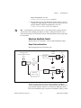
NI PXIe-5450
User Manual
National Instruments 400 MS/s, 16-bit differential I/Q generator for the
PXI Express platform
July 2008
372622A-01
Support
Worldwide Technical Support and Product Information
ni.com
National Instruments Corporate Headquarters
11500 North Mopac Expressway Austin, Texas 78759-3504 USA Tel: 512 683 0100
Worldwide Offices
Australia 1800 300 800, Austria 43 662 457990-0, Belgium 32 (0) 2 757 0020, Brazil 55 11 3262 3599,
Canada 800 433 3488, China 86 21 5050 9800, Czech Republic 420 224 235 774, Denmark 45 45 76 26 00,
Finland 358 (0) 9 725 72511, France 01 57 66 24 24, Germany 49 89 7413130, India 91 80 41190000,
Israel 972 3 6393737, Italy 39 02 41309277, Japan 0120-527196, Korea 82 02 3451 3400,
Lebanon 961 (0) 1 33 28 28, Malaysia 1800 887710, Mexico 01 800 010 0793, Netherlands 31 (0) 348 433 466,
New Zealand 0800 553 322, Norway 47 (0) 66 90 76 60, Poland 48 22 328 90 10, Portugal 351 210 311 210,
Russia 7 495 783 6851, Singapore 1800 226 5886, Slovenia 386 3 425 42 00, South Africa 27 0 11 805 8197,
Spain 34 91 640 0085, Sweden 46 (0) 8 587 895 00, Switzerland 41 56 2005151, Taiwan 886 02 2377 2222,
Thailand 662 278 6777, Turkey 90 212 279 3031, United Kingdom 44 (0) 1635 523545
For further support information, refer to the Technical Support and Professional Services appendix. To comment
on National Instruments documentation, refer to the National Instruments Web site at ni.com/info and enter
the info code feedback.
© 2008 National Instruments Corporation. All rights reserved.
Important Information
Warranty
The NI 5450 is warranted against defects in materials and workmanship for a period of 1 year from the date of shipment, as evidenced by
receipts or other documentation. National Instruments will, at its option, repair or replace equipment that proves to be defective during the
warranty period. This warranty includes parts and labor.
The media on which you receive National Instruments software are warranted not to fail to execute programming instructions, due to defects in
materials and workmanship, for a period of 90 days from date of shipment, as evidenced by receipts or other documentation. National Instruments
will, at its option, repair or replace software media that do not execute programming instructions if National Instruments receives notice of such defects
during the warranty period. National Instruments does not warrant that the operation of the software shall be uninterrupted or error free.
A Return Material Authorization (RMA) number must be obtained from the factory and clearly marked on the outside of the package before any
equipment will be accepted for warranty work. National Instruments will pay the shipping costs of returning to the owner parts which are covered by
warranty.
National Instruments believes that the information in this document is accurate. The document has been carefully reviewed for technical accuracy. In
the event that technical or typographical errors exist, National Instruments reserves the right to make changes to subsequent editions of this document
without prior notice to holders of this edition. The reader should consult National Instruments if errors are suspected. In no event shall National
Instruments be liable for any damages arising out of or related to this document or the information contained in it.
EXCEPT AS SPECIFIED HEREIN, NATIONAL INSTRUMENTS MAKES NO WARRANTIES, EXPRESS OR IMPLIED, AND SPECIFICALLY DISCLAIMS ANY WARRANTY OF
MERCHANTABILITY OR FITNESS FOR A PARTICULAR PURPOSE. CUSTOMER’S RIGHT TO RECOVER DAMAGES CAUSED BY FAULT OR NEGLIGENCE ON THE PART OF NATIONAL
INSTRUMENTS SHALL BE LIMITED TO THE AMOUNT THERETOFORE PAID BY THE CUSTOMER. NATIONAL INSTRUMENTS WILL NOT BE LIABLE FOR DAMAGES RESULTING
FROM LOSS OF DATA, PROFITS, USE OF PRODUCTS, OR INCIDENTAL OR CONSEQUENTIAL DAMAGES, EVEN IF ADVISED OF THE POSSIBILITY THEREOF. This limitation of
the liability of National Instruments will apply regardless of the form of action, whether in contract or tort, including negligence. Any action against
National Instruments must be brought within one year after the cause of action accrues. National Instruments shall not be liable for any delay in
performance due to causes beyond its reasonable control. The warranty provided herein does not cover damages, defects, malfunctions, or service
failures caused by owner’s failure to follow the National Instruments installation, operation, or maintenance instructions; owner’s modification of the
product; owner’s abuse, misuse, or negligent acts; and power failure or surges, fire, flood, accident, actions of third parties, or other events outside
reasonable control.
Copyright
Under the copyright laws, this publication may not be reproduced or transmitted in any form, electronic or mechanical, including photocopying,
recording, storing in an information retrieval system, or translating, in whole or in part, without the prior written consent of National
Instruments Corporation.
National Instruments respects the intellectual property of others, and we ask our users to do the same. NI software is protected by copyright and other
intellectual property laws. Where NI software may be used to reproduce software or other materials belonging to others, you may use NI software only
to reproduce materials that you may reproduce in accordance with the terms of any applicable license or other legal restriction.
Trademarks
National Instruments, NI, ni.com, and LabVIEW are trademarks of National Instruments Corporation. Refer to the Terms of Use section
on ni.com/legal for more information about National Instruments trademarks.
Other product and company names mentioned herein are trademarks or trade names of their respective companies.
Members of the National Instruments Alliance Partner Program are business entities independent from National Instruments and have no agency,
partnership, or joint-venture relationship with National Instruments.
Patents
For patents covering National Instruments products/technology, refer to the appropriate location: Help»Patents in your software,
the patents.txt file on your media, or the National Instruments Patent Notice at ni.com/patents.
WARNING REGARDING USE OF NATIONAL INSTRUMENTS PRODUCTS
(1) NATIONAL INSTRUMENTS PRODUCTS ARE NOT DESIGNED WITH COMPONENTS AND TESTING FOR A LEVEL OF
RELIABILITY SUITABLE FOR USE IN OR IN CONNECTION WITH SURGICAL IMPLANTS OR AS CRITICAL COMPONENTS IN
ANY LIFE SUPPORT SYSTEMS WHOSE FAILURE TO PERFORM CAN REASONABLY BE EXPECTED TO CAUSE SIGNIFICANT
INJURY TO A HUMAN.
(2) IN ANY APPLICATION, INCLUDING THE ABOVE, RELIABILITY OF OPERATION OF THE SOFTWARE PRODUCTS CAN BE
IMPAIRED BY ADVERSE FACTORS, INCLUDING BUT NOT LIMITED TO FLUCTUATIONS IN ELECTRICAL POWER SUPPLY,
COMPUTER HARDWARE MALFUNCTIONS, COMPUTER OPERATING SYSTEM SOFTWARE FITNESS, FITNESS OF COMPILERS
AND DEVELOPMENT SOFTWARE USED TO DEVELOP AN APPLICATION, INSTALLATION ERRORS, SOFTWARE AND HARDWARE
COMPATIBILITY PROBLEMS, MALFUNCTIONS OR FAILURES OF ELECTRONIC MONITORING OR CONTROL DEVICES,
TRANSIENT FAILURES OF ELECTRONIC SYSTEMS (HARDWARE AND/OR SOFTWARE), UNANTICIPATED USES OR MISUSES, OR
ERRORS ON THE PART OF THE USER OR APPLICATIONS DESIGNER (ADVERSE FACTORS SUCH AS THESE ARE HEREAFTER
COLLECTIVELY TERMED “SYSTEM FAILURES”). ANY APPLICATION WHERE A SYSTEM FAILURE WOULD CREATE A RISK OF
HARM TO PROPERTY OR PERSONS (INCLUDING THE RISK OF BODILY INJURY AND DEATH) SHOULD NOT BE RELIANT SOLELY
UPON ONE FORM OF ELECTRONIC SYSTEM DUE TO THE RISK OF SYSTEM FAILURE. TO AVOID DAMAGE, INJURY, OR DEATH,
THE USER OR APPLICATION DESIGNER MUST TAKE REASONABLY PRUDENT STEPS TO PROTECT AGAINST SYSTEM FAILURES,
INCLUDING BUT NOT LIMITED TO BACK-UP OR SHUT DOWN MECHANISMS. BECAUSE EACH END-USER SYSTEM IS
CUSTOMIZED AND DIFFERS FROM NATIONAL INSTRUMENTS' TESTING PLATFORMS AND BECAUSE A USER OR APPLICATION
DESIGNER MAY USE NATIONAL INSTRUMENTS PRODUCTS IN COMBINATION WITH OTHER PRODUCTS IN A MANNER NOT
EVALUATED OR CONTEMPLATED BY NATIONAL INSTRUMENTS, THE USER OR APPLICATION DESIGNER IS ULTIMATELY
RESPONSIBLE FOR VERIFYING AND VALIDATING THE SUITABILITY OF NATIONAL INSTRUMENTS PRODUCTS WHENEVER
NATIONAL INSTRUMENTS PRODUCTS ARE INCORPORATED IN A SYSTEM OR APPLICATION, INCLUDING, WITHOUT
LIMITATION, THE APPROPRIATE DESIGN, PROCESS AND SAFETY LEVEL OF SUCH SYSTEM OR APPLICATION.
Compliance
Compliance with FCC/Canada Radio Frequency Interference
Regulations
Determining FCC Class
The Federal Communications Commission (FCC) has rules to protect wireless communications from interference. The FCC
places digital electronics into two classes. These classes are known as Class A (for use in industrial-commercial locations only)
or Class B (for use in residential or commercial locations). All National Instruments (NI) products are FCC Class A products.
Depending on where it is operated, this Class A product could be subject to restrictions in the FCC rules. (In Canada, the
Department of Communications (DOC), of Industry Canada, regulates wireless interference in much the same way.) Digital
electronics emit weak signals during normal operation that can affect radio, television, or other wireless products.
All Class A products display a simple warning statement of one paragraph in length regarding interference and undesired
operation. The FCC rules have restrictions regarding the locations where FCC Class A products can be operated.
Consult the FCC Web site at www.fcc.gov for more information.
FCC/DOC Warnings
This equipment generates and uses radio frequency energy and, if not installed and used in strict accordance with the instructions
in this manual and the CE marking Declaration of Conformity*, may cause interference to radio and television reception.
Classification requirements are the same for the Federal Communications Commission (FCC) and the Canadian Department
of Communications (DOC).
Changes or modifications not expressly approved by NI could void the user’s authority to operate the equipment under the
FCC Rules.
Class A
Federal Communications Commission
This equipment has been tested and found to comply with the limits for a Class A digital device, pursuant to part 15 of the FCC
Rules. These limits are designed to provide reasonable protection against harmful interference when the equipment is operated
in a commercial environment. This equipment generates, uses, and can radiate radio frequency energy and, if not installed and
used in accordance with the instruction manual, may cause harmful interference to radio communications. Operation of this
equipment in a residential area is likely to cause harmful interference in which case the user is required to correct the interference
at their own expense.
Canadian Department of Communications
This Class A digital apparatus meets all requirements of the Canadian Interference-Causing Equipment Regulations.
Cet appareil numérique de la classe A respecte toutes les exigences du Règlement sur le matériel brouilleur du Canada.
Compliance with EU Directives
Users in the European Union (EU) should refer to the Declaration of Conformity (DoC) for information* pertaining to the
CE marking. Refer to the Declaration of Conformity (DoC) for this product for any additional regulatory compliance
information. To obtain the DoC for this product, visit ni.com/certification, search by model number or product line,
and click the appropriate link in the Certification column.
* The CE marking Declaration of Conformity contains important supplementary information and instructions for the user or
installer.
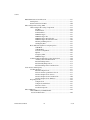
Contents
About This Manual
Conventions ...................................................................................................................xiii
Related Documentation..................................................................................................xiv
Chapter 1
Features Supported on SMC Devices
Chapter 2
NI 5450 Overview
Front Panel .....................................................................................................................2-2
Differential Channel Connectors.....................................................................2-4
Load Impedance Compensation........................................................2-5
CLK IN Connector ..........................................................................................2-5
External Reference Clock Input ........................................................2-5
External Sample Clock Input ............................................................2-6
External Sample Clock Timebase Input............................................2-6
CLK OUT Connector ......................................................................................2-7
PFI Connectors ................................................................................................2-7
ACCESS and ACTIVE LEDs .........................................................................2-8
ACCESS LED...................................................................................2-8
ACTIVE LED ...................................................................................2-8
Power-Up and Reset Conditions....................................................................................2-9
Thermal Shutdown.........................................................................................................2-10
Theory of Operation.......................................................................................................2-11
Block Diagram.................................................................................................2-11
Hardware State Diagram .................................................................................2-12
Analog Output .................................................................................................2-14
Waveform Amplitude Control ..........................................................2-15
Output Paths and Amplifiers ..............................................2-15
Attenuation .........................................................................2-16
Analog Gain Settings..........................................................2-16
Digital Gain ........................................................................2-17
Flatness Correction .............................................................2-17
Filtering Effects.................................................................................2-17
Output Enable ...................................................................................2-18
Multichannel Configuration ............................................................................2-19
Configuring Channels for OSP .........................................................2-19
© National Instruments Corporation
vii
NI PXIe-5450 User Manual
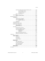
Contents
Multichannel Waveform Allocation ............................................................... 2-19
Writing Data ..................................................................................... 2-19
Interleaved Waveform Data.............................................................. 2-20
Onboard Signal Processing (OSP) .................................................................. 2-21
Onboard Signal Processing Components ......................................... 2-21
I/Q Rate .............................................................................. 2-22
Prefilter Gain ...................................................................... 2-22
Prefilter Offset.................................................................... 2-22
FIR Filter Types ................................................................. 2-23
FIR Filter Type: Flat .......................................................... 2-24
FIR Filter Type: Raised Cosine.......................................... 2-25
FIR Filter Type: Root Raised Cosine................................. 2-26
Filtering and Interpolation.................................................. 2-27
Writing I/Q Data................................................................. 2-27
Basic Onboard Signal Processing Properties.................................... 2-27
OSP Mode .......................................................................... 2-27
OSP Enabled ...................................................................... 2-28
Data Processing Mode........................................................ 2-28
IQ Rate ............................................................................... 2-28
Frequency Shift .................................................................. 2-29
FIR Filter Type................................................................... 2-30
Common Onboard Signal Processing Applications ......................... 2-30
Arbitrary Waveform Generation ........................................ 2-30
Baseband Interpolation....................................................... 2-31
Baseband I/Q Interpolation ................................................ 2-32
Baseband Interpolation Considerations.............................. 2-33
Clock Source and Frequency .......................................................................... 2-35
Clocking Options .............................................................................. 2-35
Internal Sample Clock........................................................ 2-37
Phase-Locked Loop Reference Clock ................................ 2-37
External Sample Clock Sources ......................................... 2-39
External Sample Clock Considerations.............................. 2-40
External Sample Clock Timebase ...................................... 2-41
Exporting Clocks .............................................................................. 2-42
Sample Clock ..................................................................... 2-42
Sample Clock Timebase..................................................... 2-43
Reference Clock ................................................................. 2-43
Destination Options............................................................ 2-43
Onboard Memory ............................................................................................ 2-44
Onboard Memory for Multichannel
Waveform Generation.................................................................... 2-46
NI PXIe-5450 User Manual
viii
ni.com
Contents
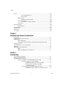
Waveform and Generation Instruction Memory Size .......................2-46
Waveform Memory Size ....................................................2-46
Instruction Memory Size ....................................................2-48
Total Memory Size .............................................................2-49
Memory Fragmentation.....................................................................2-54
Signal Routing .................................................................................................2-55
Syntax for Terminal Names ..............................................................2-56
Waveform Generation....................................................................................................2-56
Output Modes ..................................................................................................2-56
Arbitrary Waveform Mode ...............................................................2-57
Arbitrary Sequence Mode .................................................................2-57
Segment Components .........................................................2-60
Script Mode.......................................................................................2-60
Aborting Generation........................................................................................2-62
Sample Size and Resolution ............................................................................2-62
Waveform Size and Quantum .........................................................................2-62
Waveform Size..................................................................................2-62
Waveform Quantum..........................................................................2-63
Streaming.........................................................................................................2-64
Streaming Waveform Data................................................................2-64
Streaming to Multiple Channels .......................................................2-69
Average Performance Rates..............................................................2-69
PXI and PCI........................................................................2-69
PXI Express ........................................................................2-69
Improving Streaming Performance ...................................................2-70
PXI Express Bandwidth Considerations ...........................................2-71
Triggering ......................................................................................................................2-72
Triggers Summary ...........................................................................................2-73
Types of Triggers ............................................................................................2-73
Edge Trigger .....................................................................................2-74
Level Trigger.....................................................................................2-74
Software Trigger ...............................................................................2-74
Trigger Sources ...............................................................................................2-74
Trigger Modes .................................................................................................2-75
Single Trigger Mode .........................................................................2-76
Continuous Trigger Mode.................................................................2-77
Stepped Trigger Mode ......................................................................2-78
Burst Trigger Mode...........................................................................2-79
Trigger Timing ................................................................................................2-80
Filtering Effects ...............................................................................................2-80
Data Mask ......................................................................................................................2-81
© National Instruments Corporation
ix
NI PXIe-5450 User Manual
Contents
Events ............................................................................................................................ 2-81
Event Output Behaviors.................................................................... 2-81
Event Status ...................................................................................... 2-81
Marker Events ................................................................................................. 2-83
Markers as Trigger Outputs .............................................................. 2-84
Data Marker Events ........................................................................................ 2-84
Data Markers as Trigger Outputs ..................................................... 2-85
Event Delays ................................................................................................... 2-85
Exporting Signals .......................................................................................................... 2-86
Routing Signals ............................................................................................... 2-88
Synchronization............................................................................................................. 2-89
Specifications ................................................................................................................ 2-89
Calibration ..................................................................................................................... 2-89
Accessories .................................................................................................................... 2-89
Chapter 3
Integration and System Considerations
Environment .................................................................................................................. 3-1
PXI/PXI Express Chassis Cooling ................................................................................ 3-3
PXI Modules.................................................................................................................. 3-3
Chassis Guidelines .......................................................................................... 3-4
Using PXI-Compatible Products with Standard CompactPCI Products......... 3-4
PXI Trigger Lines.......................................................................................................... 3-5
System Reference Clock, PXI_CLK10 ......................................................................... 3-6
PFI Lines ....................................................................................................................... 3-6
MXI Optimization Application ..................................................................................... 3-7
MXI-3.............................................................................................................. 3-7
MXI-4 and MXI-Express Optimization .......................................................... 3-7
Chapter 4
Programming
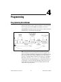
Programming State Model............................................................................................. 4-1
General Programming Flow .......................................................................................... 4-3
Instrument Driver Overview.......................................................................................... 4-4
Creating an Application with NI-FGEN and Your ADE ................................ 4-5
Creating an Application with LabVIEW .......................................... 4-5
NI-FGEN Example Programs for LabVIEW ..................... 4-5
Considerations for using the LabVIEW
Real-Time Module .......................................................... 4-6
Creating an Application with LabWindows/CVI ............................. 4-7
NI-FGEN Example Programs for LabWindows/CVI ........ 4-7
NI PXIe-5450 User Manual
x
ni.com
Contents
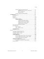
Creating an Application with Visual C/C++.....................................4-7
NI-FGEN Example Programs for Visual C/C++................4-8
Special Considerations .......................................................4-8
Parameter Passing...............................................................4-8
Creating an Application with Visual Basic.......................................4-8
NI-FGEN Tutorial..........................................................................................................4-9
Example Programs...........................................................................................4-9
Basic Steps.......................................................................................................4-9
Initialize...........................................................................................................4-10
Configuration...................................................................................................4-11
Configure Channels...........................................................................4-11
Configure Output Mode ....................................................................4-12
Configure Standard Function Mode ...................................4-12
Configure Arbitrary Waveform Mode................................4-13
Configure Arbitrary Sequence Mode .................................4-14
Configure Frequency List Mode.........................................4-16
Configure Script Mode .......................................................4-17
Initiate Generation ...........................................................................................4-19
Abort Generation .............................................................................................4-19
Abort to Ground ................................................................................4-19
Abort to a Known Voltage ................................................................4-20
Closing the Session..........................................................................................4-21
NI-FGEN Error Codes.....................................................................................4-21
Features ..........................................................................................................................4-23
Configuring an Internal Sample Clock............................................................4-23
Configuring an External Sample Clock...........................................................4-24
Configuring a Reference Clock .......................................................................4-24
Configuring Triggers .......................................................................................4-25
Creating a Marker Event .................................................................................4-26
Creating a Marker Event in Arbitrary Waveform Mode...................4-26
Creating a Marker Event in Arbitrary Sequence Mode ....................4-27
Creating a Marker Event in Script Mode ..........................................4-27
Creating a Data Marker Event.........................................................................4-28
Configuring an Application for Streaming......................................................4-29
Configuring Your Application for Direct DMA ...............................4-31
Simulation Mode .............................................................................................4-32
© National Instruments Corporation
xi
NI PXIe-5450 User Manual
Contents
Chapter 5
Signal Generation Fundamentals
Bandwidth and Passband Flatness................................................................................. 5-1
Sample Rate................................................................................................................... 5-2
Nyquist and Shannon's Sampling Theorems................................................... 5-3
Nyquist Theorem .............................................................................. 5-3
Shannon’s Sampling Theorem.......................................................... 5-3
Aliased Images ................................................................................. 5-4
DAC Resolution .............................................................................................. 5-6
Impedance Matching ..................................................................................................... 5-7
Mismatch Uncertainty ...................................................................... 5-9
Resistive Matching ........................................................................... 5-9
Output Attenuation ........................................................................................................ 5-10
Phase-Locked Looping.................................................................................................. 5-11
Frequency Domain Fundamentals................................................................................. 5-12
SFDR............................................................................................................... 5-12
THD ................................................................................................................ 5-12
SINAD ............................................................................................................ 5-13
ENOB.............................................................................................................. 5-13
Filtering and Interpolation............................................................................................. 5-13
Appendix A
Technical Support and Professional Services
NI PXIe-5450 User Manual
xii
ni.com
About This Manual
This user manual explains the fundamental and advanced concepts
necessary for using the NI 5450 arbitrary function generator and describes
the features, functions, and operation of the signal generator.
Conventions
The following conventions are used in this manual:
<>
Angle brackets that contain numbers separated by an ellipsis represent
a range of values associated with a bit or signal name—for example,
AO <3..0>.
[]
Square brackets enclose optional items—for example, [response].
»
The » symbol leads you through nested menu items and dialog box options
to a final action. The sequence File»Page Setup»Options directs you to
pull down the File menu, select the Page Setup item, and select Options
from the last dialog box.
♦
The ♦ symbol indicates that the following text applies only to a specific
product, a specific operating system, or a specific software version.
This icon denotes a tip, which alerts you to advisory information.
This icon denotes a note, which alerts you to important information.
This icon denotes a caution, which advises you of precautions to take to
avoid injury, data loss, or a system crash. When this symbol is marked on a
product, refer to the Read Me First: Safety and Radio-Frequency
Interference document, included with the device, for information about
precautions to take.
bold
Bold text denotes items that you must select or click in the software, such
as menu items and dialog box options. Bold text also denotes parameter
names.
italic
Italic text denotes variables, emphasis, a cross-reference, or an introduction
to a key concept. Italic text also denotes text that is a placeholder for a word
or value that you must supply.
© National Instruments Corporation
xiii
NI PXIe-5450 User Manual
monospace
Text in this font denotes text or characters that you should enter from the
keyboard, sections of code, programming examples, and syntax examples.
This font is also used for the proper names of disk drives, paths, directories,
programs, subprograms, subroutines, device names, functions, operations,
variables, filenames, and extensions.
monospace bold
Bold text in this font denotes the messages and responses that the computer
automatically prints to the screen. This font also emphasizes lines of code
that are different from the other examples.
monospace italic
Italic text in this font denotes text that is a placeholder for a word or value
that you must supply.
Platform
Text in this font denotes a specific platform and indicates that the text
following it applies only to that platform.
Related Documentation
The following documents contain information that you may find helpful as
you read this manual:
NI PXIe-5450 User Manual
•
NI Signal Generators Getting Started Guide—provides instructions
for installing and configuring NI signal generators
•
NI Signal Generators Help—includes detailed information about the
NI 5450 and the NI-FGEN VIs and functions
•
NI 5450 Specifications—provides the published specification values
for the NI 5450
xiv
ni.com
1
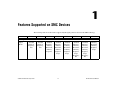
Features Supported on SMC Devices
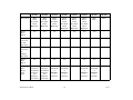
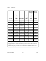
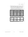
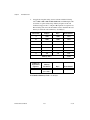
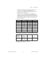
The following table shows the features supported by NI signal generators based on the SMC technology.
NI 5402
NI 5406
NI 5412
NI 5421
NI 5422
NI 5441
NI 5442
NI 5450
Standard
Function,
Frequency
List
Standard
Function,
Arbitrary
Waveform,
Arbitrary
Sequence
Standard
Function,
Arbitrary
Waveform,
Arbitrary
Sequence,
Script
Standard
Function,
Arbitrary
Waveform,
Arbitrary
Sequence,
Script
Standard
Function,
Arbitrary
Waveform,
Arbitrary
Sequence,
Script,
Frequency
List
Standard
Function,
Arbitrary
Waveform,
Arbitrary
Sequence,
Script,
Frequency
List
Arbitrary
Waveform,
Arbitrary
Sequence,
Script
Basic Operation
Output
Modes
Standard
Function,
Frequency
List
© National Instruments Corporation
1-1
NI PXIe-5450 User Manual
NI 5402
NI 5406
NI 5412
NI 5421
NI 5422
NI 5441
NI 5442
NI 5450
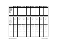
Standard Function Output
Waveform
Sine,
Square,
Triangle,
Ramp Up,
Ramp
Down, DC,
Noise,
UserDefined
Sine,
Square,
Triangle,
Ramp Up,
Ramp
Down, DC,
Noise,
UserDefined
Sine,
Square,
Triangle,
Ramp Up,
DC, Noise,
UserDefined
Sine,
Square,
Triangle,
Ramp Up,
Ramp
Down, DC,
Noise,
UserDefined
Sine,
Square,
Triangle,
Ramp Up,
Ramp
Down, DC,
Noise,
UserDefined
Sine,
Square,
Triangle,
Ramp Up,
Ramp
Down, DC,
Noise,
UserDefined
Sine,
Square,
Triangle,
Ramp Up,
Ramp
Down, DC,
Noise,
UserDefined
—
Minimum
Frequency
0 Hz
0 Hz
<1 mHz‡‡
<1 mHz‡‡
<1 mHz‡‡
0 Hz
0 Hz
—
Maximum
Frequency††
Sine:
20 MHz,
Square:
20 MHz,
UserDefined:
20 MHz,
Other:
1 MHz
Sine:
40 MHz,
Square:
40 MHz,
UserDefined:
40 MHz,
Other:
5 MHz
Sine:
20 MHz,
Square:
5 MHz,
Other:
1 MHz
Sine:
43 MHz,
Square
25 MHz,
Other:
5 MHz
Sine:
80 MHz,
Square:
100 MHz,
Other:
10 MHz
Sine:
43 MHz,
Square
25 MHz,
UserDefined:
43 MHz,
Other:
5 MHz
Sine:
43 MHz,
Square
25 MHz,
UserDefined:
43 MHz,
Other:
5 MHz
—
SYNC Duty
Cycle
20% to
80% for
square, 50%
for all other
20% to
80% for
square, 50%
for all other
—
—
—
—
—
—
16,384
samples
16,384
samples
Variable†
Variable†
Variable†
16,384
samples
32,768
samples
—
UserDefined
Waveform
Size
NI PXIe-5450 User Manual
1-2
ni.com
NI 5402
NI 5406
NI 5412
NI 5421
NI 5422
NI 5441
NI 5442
NI 5450
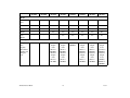
Frequency List Output
Maximum
Number of
Lists*
9,999 lists
9,999 lists
—
—
—
9,999 lists
9,999 lists
—
Maximum
List Length*
58,253 s
58,253 s
—
—
—
932,066 s
932,066 s
—
Maximum
Step
Duration*
21 s
21 s
—
—
—
21 s
21 s
—
Minimum
List Length*
1s
1s
—
—
—
1s
1s
—
Minimum
Step
Duration*
1.28 µs
1.28 µs
—
—
—
1.28 µs
1.28 µs
—
Step
Duration
Quantum*
80 ns
80 ns
—
—
—
80 ns
80 ns
—
Arbitrary Waveform Output
Write
Quantum
64 samples
or
32 complex
samples
64 samples
or
32 complex
samples
64 samples
or
32 complex
samples
64 samples
or
32 complex
samples
64 samples
or
32 complex
samples
64 samples
or
32 complex
samples
1 sample
1 sample
Waveform
Quantum*
—
—
4 samples
4 samples
4 samples
4 samples
1 sample
2 samples
© National Instruments Corporation
1-3
NI PXIe-5450 User Manual
NI 5402
NI 5406
NI 5412
NI 5421
NI 5422
NI 5441
NI 5442
NI 5450
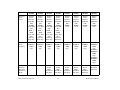
Minimum
Waveform
Write Size*
—
—
4 samples
4 samples
4 samples
4 samples
4 samples
4 samples
Maximum
Waveform
Write Size*†
—
—
4 M, 16 M,
128 M
samples
4 M, 16 M,
128 M,
256 M
samples
4 M, 16 M,
128 M,
256 M
samples
16 M,
128 M,
256 M
samples
16 M,
128 M,
256 M
samples
67 M,
108 M,
352 M
samples
Maximum
Number of
Waveforms*
—
—
2,097,151
2,097,151
2,097,151
2,097,151
2,097,151
2,097,151
Streaming
—
—
—
Yes
Yes
Yes
Yes
Yes
Onboard
Signal
Processing
—
—
—
—
—
Yes
Yes
Yes
1
1
1
1
1
1
16,777,205†
16,777,205†
16,777,205†
16,777,205†
16,777,205†
16,777,205†
Arbitrary Sequence Output
Minimum
Sequence
Length*
—
—
Maximum
Sequence
Length*
—
—
Maximum
Loop
Count*
—
—
16,777,215
16,777,215
16,777,215
16,777,215
16,777,215
16,777,215
Maximum
Number of
Sequences*
—
—
2,097,151†
2,097,151†
2,097,151†
2,097,151†
2,097,151†
2,097,151†
NI PXIe-5450 User Manual
1-4
ni.com
NI 5402
NI 5406
NI 5412
NI 5421
NI 5422
NI 5441
NI 5442
NI 5450
Streaming
—
—
—
Yes
Yes
Yes
Yes
Yes
Onboard
Signal
Processing
—
—
—
—
—
Yes
Yes
Yes
Maximum
Number of
Script
Triggers
—
—
—
4
4
4
4
4
Maximum
Number of
Markers
—
—
—
4
4
4
4
4
Streaming
—
—
—
Yes
Yes
Yes
Yes
Yes
up to ±5 V
up to ±5 V
up to ±6 V
up to ±6 V
up to ±6 V
up to ±6 V
up to ±1 V
up to ±1 V
Offset (at
maximum
gain)
±5 Vpk
±5 Vpk
±3 V
±3 V
±6 V
±3 V
±0.5 V
0V
Output
Impedance
50 Ω, 75 Ω
50 Ω, 75 Ω
50 Ω, 75 Ω
50 Ω, 75 Ω
50 Ω, 75 Ω
50 Ω, 75 Ω
50 Ω, 75 Ω
50 Ω
Script Output
Output Characteristics
Output
Voltage (at
load equal
to source
impedance)
© National Instruments Corporation
1-5
NI PXIe-5450 User Manual
NI 5402
NI 5406
NI 5412
NI 5421
NI 5422
NI 5441
NI 5442
NI 5450
Main,
Fixed
Low-Gain,
Fixed
High-Gain
Main,
Fixed
Low-Gain,
Fixed
High-Gain
Main,
Fixed
Low-Gain,
Fixed
High-Gain
Main,
Direct,
Fixed
Low-Gain,
Fixed
High-Gain
Main,
Direct,
Fixed
Low-Gain,
Fixed
High-Gain
Main,
Direct,
Fixed
Low-Gain,
Fixed
High-Gain
Main,
Direct
Direct
Analog
Filter
Option
Yes
Yes
No
Yes
Yes
Yes
Yes
—
Flatness
Correction
for Sine
Waveforms
Yes
Yes
—
—
—
—
—
Yes
Flatness
Correction
for
Arbitrary
Waveforms
—
—
—
—
—
—
—
Yes
Digital
Filter
Option
Yes
Yes
Yes
Yes
—
Yes
Yes
—
Digital
Filter
Interpolation
Factor
2 or 4
(automatic
for Standard
Function
and
Frequency
List modes)
2 or 4
(automatic
for Standard
Function
and
Frequency
List modes)
2, 4, or 8
(maximum
of
400 MS/s)
or
automatic
2, 4, or 8
(maximum
of
400 MS/s)
or
automatic
—
2, 4, or 8
(maximum
of
400 MS/s)
or
automatic
2, 4, or 8
(maximum
of
400 MS/s)
or
automatic
—
Analog Path
NI PXIe-5450 User Manual
1-6
ni.com
DIGITAL
DATA &
CONTROL
CONNECTOR
(DDC)
or Digital
Pattern
NI 5402
NI 5406
NI 5412
NI 5421
NI 5422
NI 5441
NI 5442
NI 5450
—
—
—
Optional†
Optional†
Optional†
—
—
Triggering and Synchronization
Trigger
Modes
(Frequency
List and
Arbitrary
Waveform
Generation
Modes)
Single,
Continuous,
Stepped,
Burst
Single,
Continuous,
Stepped,
Burst
Single,
Continuous,
Stepped,
Burst
Single,
Continuous,
Stepped,
Burst
Single,
Continuous,
Stepped,
Burst
Single,
Continuous,
Stepped,
Burst
Single,
Continuous,
Stepped,
Burst
Single,
Continuous,
Stepped,
Burst
Trigger
Sources
Immediate,
External,
Software,
RTSI_
<0..7>,
PXI_STAR,
PFI <0..1>
Immediate,
External,
Software,
RTSI_
<0..7>,
PXI_STAR,
PFI <0..1>
Immediate,
External,
Software,
RTSI_
<0..7>,
PXI_STAR,
PFI <0..1>
Immediate,
External,
Software,
RTSI_
<0..7>,
PXI_STAR,
PFI <0..1>
Immediate,
External,
Software,
RTSI_
<0..7>,
PXI_STAR,
PFI <0..1>
Immediate,
External,
Software,
RTSI_
<0..7>,
PXI_STAR,
PFI <0..1>
Immediate,
External,
Software,
RTSI_
<0..7>,
PXI_STAR,
PFI <0..1>
Immediate,
External,
Software,
RTSI_
<0..7>,
PFI <0..1>
Using
NI-TClk
Using
NI-TClk
Using
NI-TClk
except for
Standard
Function
mode
Using
NI-TClk
except for
Standard
Function
mode
Using
NI-TClk
except for
Standard
Function
mode
Using
NI-TClk
Using
NI-TClk
Using
NI-TClk
Multiple
Device
Synchronization
© National Instruments Corporation
1-7
NI PXIe-5450 User Manual
NI 5402
NI 5406
NI 5412
NI 5421
NI 5422
NI 5441
NI 5442
NI 5450
Ready for
Start
Yes
Yes
Yes
Yes
Yes
Yes
Yes
Yes
Started
Yes
Yes
Yes
Yes
Yes
Yes
Yes
Yes
Done
Yes
Yes
Yes
Yes
Yes
Yes
Yes
Yes
Marker
—
—
Yes
Yes
Yes
Yes
Yes
Yes
Data
Marker
—
—
—
Yes
Yes
Yes
Yes
Yes
100 MS/s
100 MS/s
Internal
Sample
clock:
10 S/s to
100 MS/s,
External
Sample
clock:
10 S/s to
105 MS/s
Internal
Sample
clock:
10 S/s to
100 MS/s,
External
Sample
clock:
10 S/s to
105 MS/s
5 MS/s to
200 MS/s
Internal
Sample
clock:
10 S/s to
100 MS/s,
External
Sample
clock:
10 S/s to
105 MS/s
Internal
Sample
clock:
10 S/s to
100 MS/s,
External
Sample
clock:
10 S/s to
105 MS/s
Internal
Sample
clock:
12.2 kS/s to
400 MS/s,
External
Sample
clock:
10 MS/s,
20 MS/s to
400 MS/s
Events
Clocking
Sample
Rate
(Update
Rate) before
filtering and
interpolation
NI PXIe-5450 User Manual
1-8
ni.com
NI 5402
NI 5406
NI 5412
NI 5421
NI 5422
NI 5441
NI 5442
NI 5450
Reference
Clock
Source
Internal
(none),
External
(CLK IN),
PXI
10 MHz
clock (PXI
only),
RTSI_7
(RTSI
clock; PCI
only),
Onboard
(PCI only)
Internal
(none),
External
(CLK IN),
PXI
10 MHz
clock (PXI
only),
RTSI_7
(RTSI
clock; PCI
only),
Onboard
(PCI only)
Internal
(none),
External
(CLK IN),
PXI
10 MHz
clock (PXI
only),
RTSI_7
(RTSI
clock; PCI
only),
Onboard
(PCI only)
Internal
(none),
External
(CLK IN),
PXI
10 MHz
clock (PXI
only),
RTSI_7
(RTSI
clock; PCI
only),
Onboard
(PCI only)
Internal
(none),
External
(CLK IN),
PXI
10 MHz
clock
Internal
(none),
External
(CLK IN),
PXI
10 MHz
clock
Internal
(none),
External
(CLK IN),
PXI
10 MHz
clock
Internal
(none),
External
(CLK IN),
PXI
10 MHz
clock
Reference
Clock
Frequency
5 MHz to
20 MHz in
1 MHz
steps
5 MHz to
20 MHz in
1 MHz
steps
5 MHz to
20 MHz in
1 MHz
steps
5 MHz to
20 MHz in
1 MHz
steps
5 MHz to
20 MHz in
1 MHz
steps
5 MHz to
20 MHz in
1 MHz
steps
5 MHz to
20 MHz in
1 MHz
steps
1 to
100 MHz in
1 MHz
steps,
102 MHz to
200 MHz in
2 MHz
steps,
204 MHz to
400 MHz in
4 MHz
steps
—
—
DivideDown,
HighResolution,
Automatic
DivideDown,
HighResolution,
Automatic
DivideDown,
HighResolution,
Automatic
DivideDown,
HighResolution,
Automatic
DivideDown,
HighResolution,
Automatic
HighResolution,
Automatic
Clock Mode
(Arbitrary
Waveform
Generation
Mode)
© National Instruments Corporation
1-9
NI PXIe-5450 User Manual
NI 5402
NI 5406
NI 5412
NI 5421
NI 5422
NI 5441
NI 5442
NI 5450
—
—
Internal,
External
(CLK IN),
PXI_STAR
(PXI only),
RTSI_
<0..7>
Internal,
External
(CLK IN),
DDC CLK
IN†,
PXI_STAR
(PXI only),
RTSI_
<0..7>
Internal,
External
(CLK IN),
DDC CLK
IN†,
PXI_STAR
Internal,
External
(CLK IN),
DDC CLK
IN†,
PXI_STAR
Internal,
External
(CLK IN),
PXI_STAR
Internal,
External
(CLK IN)
SelfCalibration
Functions
niFgen_Se
lfCal,
niFgen_Re
storeLast
ExtCalCon
stants
niFgen_Se
lfCal,
niFgen_Re
storeLast
ExtCalCon
stants
niFgen_Se
lfCal,
niFgen_Re
storeLast
ExtCalCon
stants
niFgen_Se
lfCal,
niFgen_Re
storeLast
ExtCalCon
stants
niFgen_Se
lfCal,
niFgen_Re
storeLast
ExtCalCon
stants
niFgen_Se
lfCal,
niFgen_Re
storeLast
ExtCalCon
stants
niFgen_Se
lfCal,
niFgen_Re
storeLast
ExtCalCon
stants
niFgen_Se
lfCal,
niFgen_Re
storeLast
ExtCalCon
stants
Calibration
Utility
Functions‡
niFgen_
niFgen_
niFgen_
niFgen_
niFgen_
niFgen_
niFgen_
niFgen_
functions
functions
functions
functions
functions
functions
functions
functions
Sample
Clock
Source
(Arbitrary
Waveform
Generation
Mode)
Calibration
NI PXIe-5450 User Manual
1-10
ni.com
External
Calibration
Functions∗∗
NI 5402
NI 5406
NI 5412
NI 5421
NI 5422
NI 5441
NI 5442
NI 5450
niFgen_In
itExtCal
niFgen_In
itExtCal
niFgen_In
itExtCal
niFgen_In
itExtCal
niFgen_In
itExtCal
niFgen_In
itExtCal
niFgen_In
itExtCal
niFgen_In
itExtCal
and
associated
functions
and
associated
functions
and
associated
functions
and
associated
functions
and
associated
functions
and
associated
functions
and
associated
functions
and
associated
functions
* You
can get the value of this characteristic by calling a query function or by reading an attribute. NI recommends that your programs query or read the characteristic rather
than depend on a certain value.
† Varies with the device model or the amount of memory on the device. Memory use is a function of the number and size of waveforms and (in Arbitrary Sequence mode) the
number and length of sequences. Typically, waveforms use most of the memory, but if you have a very large number of sequences, the available waveform memory is
reduced.
‡ Calibration utility functions include:
niFgen_GetSelfCalSupported, niFgen_GetSelfCalLastDateAndTime,
niFgen_GetExtCalLastDateAndTime, niFgen_GetSelfCalLastTemp,
niFgen_GetExtCalLastTemp, niFgen_GetExtCalRecommendedInterval,
niFgen_ChangeExtCalPassword, niFgen_SetCalUserDefinedInfo,
niFgen_GetCalUserDefinedInfo, niFgen_GetCalUserDefinedInfoMaxSize,
niFgen_ReadCurrentTemperature
∗∗
External calibration functions and steps vary from device to device. For more information about calibrating your device, refer to the calibration procedure for your device.
Refer to the device specifications for conditions.
‡‡ The minimum frequency available on these devices depends on the memory size of the device, as well as the value of the
NIFGEN_ATTR_FUNC_MAX_BUFFER_SIZE attribute.
††
© National Instruments Corporation
1-11
NI PXIe-5450 User Manual
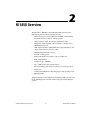
2
NI 5450 Overview
The NI 5450 is a 400 MS/s, 16-bit differential I/Q generator for the
PXI Express platform with the following features:
•
Onboard signal processing (OSP) with 120 MHz of baseband I/Q
bandwidth, flatness correction, and interpolation
•
16-bit resolution output, two channels, differential output
•
Differential output amplitude with a maximum of 1.0 Vpk-pk into a
100 Ω differential load
•
50 Ω output impedance (100 Ω differential output impedance), and
output attenuation levels from 0 to 3 dB
•
High-Resolution internal clocking
•
External clocking options
•
PLL synchronization to external clocks or to PXI clock
•
TClk synchronization
•
Sample rate up to 400 MS/s
•
Up to 2 GB of onboard waveform memory
•
Waveform linking and looping for arbitrary waveform generation
•
Digital gain
•
2 bidirectional PFI lines for importing triggers and exporting events
•
PXI trigger lines
All NI 5450 devices follow industry-standard Plug and Play specifications
for the PXI Express bus and offer seamless integration with compliant
systems.
© National Instruments Corporation
2-1
NI PXIe-5450 User Manual
Chapter 2
NI 5450 Overview
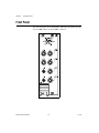
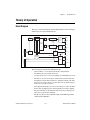
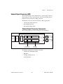
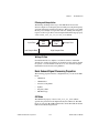
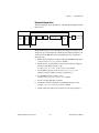
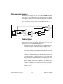
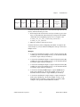
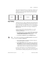
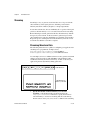
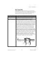
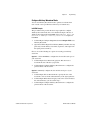
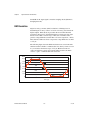
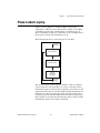
Front Panel
The following figure shows the NI PXIe-5450 front panel. This front panel
has two SMB connectors and six SMA connectors.
NI PXIe-5450 User Manual
2-2
ni.com
Chapter 2
NI 5450 Overview
The CLK IN SMA connector accepts an external clock that can be used as
a Reference clock, a Sample clock, or a Sample clock timebase.
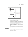
The CLK OUT SMA connector provides a clock signal that can be shared
by other devices.
The PFI 0 and PFI 1 SMB connectors are bidirectional connections that can
accept a trigger from an external source and can start or step through
waveform generation or route signals from several clock, event, and trigger
sources.
The CH 0+/I+ SMA connector provides differential waveform output for
channel 0.
The CH 0−/I− SMA connector provides complementary differential
waveform output for channel 0.
The CH 1+/Q+ SMA connector provides differential waveform output for
channel 1.
The CH 1−/Q− SMA connector provides complementary differential
waveform output for channel 0.
© National Instruments Corporation
2-3
NI PXIe-5450 User Manual
Chapter 2
NI 5450 Overview
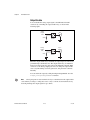
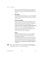
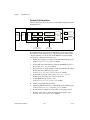
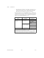
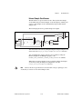
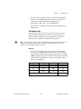
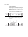
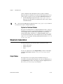
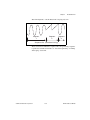
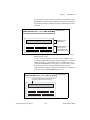
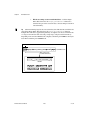
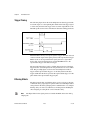
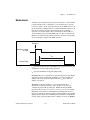
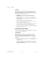
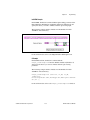
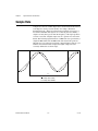
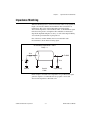
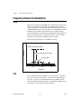
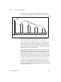
Differential Channel Connectors
The CH 0+/− and CH 1+/− connectors are the analog waveform output
terminals. These connectors provide differential waveform output; they
cannot be used for single-ended operation. The connectors must terminate
into balanced loads. The maximum output levels from these connectors
depend on the type of load termination. For example, if the output of the
device terminates into a balanced 50 Ω load with flatness correction
disabled, the maximum output levels are ±0.5 V, while the maximum
output levels are ±1.0 when the device terminates into a high-impedance
load (HiZ). This difference is illustrated in the following figure.
NI 5450
NI 5450
Load
+
RO =
50 Ω
Load
+
RL =
50 Ω
RO =
50 Ω
RL =
HiZ
±1.0 V
±0.5 V
-
RO =
50 Ω
-
RL =
50 Ω
50 Ω Load
RO =
50 Ω
RL =
HiZ
High-Impedance Load
If the output terminates into any other load, the levels are defined by the
following formula:
Vout = ± [ RL / ( RL + RO ) ] × 2 V
where
Vout is the maximum peak output voltage level
RL is the load impedance in ohms
RO is the output impedance of the module in ohms
Note For loads less than 50 Ω, load impedance compensation supports only combinations
of gain and load impedance that meet the previous Vout equation.
Set the amplitude of the generated output signal in terms of peak voltage by
setting the gain value. NI-FGEN calculates and sets the correct amount of
attenuation required for the desired gain value. Configure the output signal
NI PXIe-5450 User Manual
2-4
ni.com
Chapter 2
NI 5450 Overview
amplitude by calling the Arbitrary Waveform Gain property or
NIFGEN_ATTR_ARB_GAIN attribute.
Load Impedance Compensation
The NI 5450 has the ability to configure the output signal amplitude based
on a user-configured load impedance setting. This capability is desirable
when you use the NI 5450 with loads that are between 0 Ω and a high
impedance. Refer to the device specifications for information about the
output impedance tolerance.
By default, NI-FGEN assumes that the load impedance is equal to the
output impedance. If they do not match, you can change the load
impedance value that NI-FGEN uses in its load impedance compensation
algorithm. NI-FGEN takes the load impedance into account when setting
the amplitude and provides the amplitude specified in the configured gain
setting, eliminating the need to use the voltage divider equation. NI-FGEN
compensates to give the desired peak-to-peak voltage amplitude or
arbitrary gain (relative to 1 V). You can configure the load impedance by
calling the Load Impedance property or
NIFGEN_ATTR_LOAD_IMPEDANCE attribute.
The voltage output levels are set in the software and are based upon a 50 Ω load
termination (the default), or based on the user–specified load resistance.
Note
For waveform output signal specifications, refer to the device
specifications.
CLK IN Connector
The CLK IN front panel connector can accept an external Reference clock,
external Sample clock, or external Sample clock timebase.
Caution Do not change the external clocks while generating waveforms. Only modify the
frequency of the external clock before you start the waveform generation or after you stop
the waveform generation. NI cannot guarantee the quality of the generated signal if you
change the external clock during waveform generation.
External Reference Clock Input
The CLK IN connector can accept a Reference clock from an external
source and phase-lock the internal clock of the signal generator to this
external Reference clock. Refer to the device specifications for the
allowable Reference clock frequencies and signal characteristics.
© National Instruments Corporation
2-5
NI PXIe-5450 User Manual
Chapter 2
NI 5450 Overview
The Reference clock uses the internal clock by default. Call the niFgen
Configure Reference Clock VI or the
niFgen_ConfigureReferenceClock function to configure the
Reference clock source.
When configuring an external Reference clock, you must configure the
external Reference clock frequency if it is different from the 10 MHz
default setting. Set the Reference clock frequency with the niFgen
Configure Reference Clock VI or the
niFgen_ConfigureReferenceClock function.
You also can phase-lock the signal generator to other NI devices using the common
PXI 10 MHz backplane clock on PXI devices.
Note
External Sample Clock Input
In addition to phase-locking, the CLK IN connector also can receive an
external Sample clock. Refer to the device specifications for the allowable
external Sample clock frequencies and signal characteristics.
When configuring an external Sample clock, set the sample rate to the exact
frequency you are using to avoid data errors. Set the sample rate by calling the niFgen Set
Sample Rate VI or niFgen_ConfigureSampleRate function.
Tip
Configure the Sample clock source with niFgen Configure Sample Clock
Source VI or the niFgen_ConfigureSampleClockSource function.
The Sample clock uses the internal clock by default.
External Sample Clock Timebase Input
The CLK IN connector also can receive an external Sample clock timebase.
Refer to the device specifications for the allowable external Sample clock
timebase frequencies and signal characteristics.
Configure the Sample clock timebase source with the Sample Clock
Timebase Source and Sample Clock Timebase Rate properties or the
NIFGEN_ATTR_SAMPLE_CLOCK_TIMEBASE_SOURCE and
NIFGEN_ATTR_SAMPLE_CLOCK_TIMEBASE_RATE attributes. The device
uses the internal sample clock timebase by default.
NI PXIe-5450 User Manual
2-6
ni.com
Chapter 2
NI 5450 Overview
CLK OUT Connector
The CLK OUT connector is typically used as an output terminal to provide
a clock signal that can be shared by other devices. The CLK OUT
connector is designed to allow the NI 5450 to generate high speed clock
signals with very low jitter.
As an output, the CLK OUT line routes a signal out from the following
sources:
•
PLL Reference clock source
•
Sample Clock Out (with /K where K is an integer used to divide the
Sample clock)
•
Sample clock timebase (with /M where M is an integer used to divide
the Sample clock timebase frequency)
Refer to the device specifications for information about the signal
characteristics for the CLK OUT connector.
PFI Connectors
PFI 0 and PFI 1 are bidirectional connectors. As an input, the PFI terminals
can accept a trigger from an external source that can start or step through
waveform generation.
As an output, the PFI lines route a signal out from the following sources:
•
Marker events
•
Start trigger
•
PLL Reference clock source
•
Sample Clock Out (with /K where K is an integer used to divide the
Sample clock)
•
Started, Done, and Ready for Start events
•
Sample clock timebase (with /M where M is an integer used to divide
the Sample clock timebase frequency)
•
Script trigger
Refer to the device specifications for information about acceptable input
signal characteristics for the PFI lines and output signal characteristics.
© National Instruments Corporation
2-7
NI PXIe-5450 User Manual
Chapter 2
NI 5450 Overview
ACCESS and ACTIVE LEDs
The ACCESS and ACTIVE LEDs indicate the status of the PXIe module:
ACCESS LED
The ACCESS LED indicates basic hardware status as shown in the
following table.
Color
Indications
Off
Device is not yet functional, or the device has
detected a problem with a power rail.
Amber
The device is being accessed.
Green
The device is ready to be programmed by
NI-FGEN.
ACTIVE LED
The ACTIVE LED indicates the device state as shown in the following
table.
Color
NI PXIe-5450 User Manual
Indications
Off
Device is not generating.
Amber
The device is armed and waiting for a trigger.
Green
The device has received a trigger. Also indicates
that the device is generating a waveform.
Red
The device has detected an error. NI-FGEN must
access the device to determine the cause of the
error. The LED remains red until the error condition
is removed. Errors might include unlocked PLLs or
an over-temperature condition.
2-8
ni.com
Chapter 2
NI 5450 Overview
Power-Up and Reset Conditions
The signal generator is in the following state from the time at which the
computer begins to power up until the operating system is fully booted and
NI-FGEN is loaded.
•
The CH 0+/− and CH 1+/− differential output connectors are disabled
and each has 50 Ω impedance to ground. This impedance is the same
as its previous setting before the device was powered down. The output
voltage amplitude of this connector is 0 V.
•
The CLK IN connector has high-impedance to ground.
•
PFI 0 and PFI 1 are tristated and have a 10 kΩ impedance to ground.
•
The CLK OUT connector is tristated and has a high-impedance to
ground.
•
PXI trigger lines are tristated and floating.
After the operating system is fully booted and NI-FGEN is loaded, or when
you perform a hard reset to the device directly from MAX or using
NI-FGEN, the signal generator is in the following state:
•
CH 0+/− and CH 1+/− output is enabled.
•
CH 0+/− and CH 1+/− output attenuation is set to 0 dB.
•
CLK OUT output impedance is set to high-impedance.
•
CLK IN is disabled and has a high-impedance to ground.
•
PFI 0 and PFI 1 are tristated and have a 10 kΩ impedance to ground.
•
PXI trigger lines are tristated and floating.
•
The sample rate is set to the maximum rate, with the Sample clock
source set to the internal Sample clock timebase.
•
The Sample clock timebase is tuned by the internal reference control
voltage.
© National Instruments Corporation
2-9
NI PXIe-5450 User Manual
Chapter 2
NI 5450 Overview
Thermal Shutdown
NI-FGEN supports thermal shutdown capability for the NI 5450. This
capability allows the signal generator to detect when it has reached a
dangerously high temperature and to then power down to prevent damage
to the device.
Air circulation paths, fan settings, and space allowances are several factors
that can influence device temperature. To prevent thermal shutdown, follow
the guidelines described in the Maintain Forced-Air Cooling Note to Users
document that shipped with your device. Refer to the device specifications
to find the correct operating temperature range.
In the event that the signal generator powers down, you are notified with an
error message in one of the following ways:
•
NI-FGEN returns an error when you use any of the VIs or functions
that program the hardware or check hardware status, for example, the
niFgen Commit VI or the niFgen_commit function and the niFgen
Self Cal VI or the niFgen_SelfCal function.
•
MAX returns an error message if you run a self-test on your device
after it exceeds the thermal shutdown temperature.
To re-enable your device after thermal shutdown, use one of the following
methods:
•
Power down the computer or chassis that contains the signal generator.
or
•
Call the niFgen Reset Device VI or the niFgen_ResetDevice
function or perform a device reset in MAX. For more information
about resetting a device in MAX, select Help»Help Topics»
NI-DAQmx»MAX Help for NI-DAQmx within MAX.
Review the guidelines in the Maintain Forced-Air Cooling Note to Users
document that shipped with the product and make any necessary
adjustments to ensure that the signal generator cools effectively. The
thermal shutdown error continues to be reported until the device is
successfully reset.
NI PXIe-5450 User Manual
2-10
ni.com
Chapter 2
NI 5450 Overview
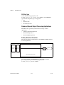
Theory of Operation
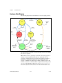
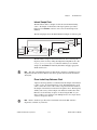
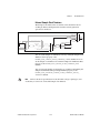
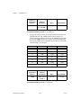
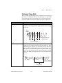
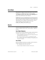
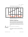
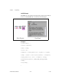
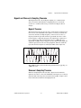
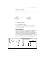
Block Diagram
This topic contains information about the NI 5450 top-level block diagram
and descriptions of the individual blocks.
Synchronization
and Memory Core
Waveform
Generation
Engine
Onboard
Memory
Digital
Gain 0
CH 0+
Analog
Output Path
with Lowpass
Filters 0
DAC 0
CH 0-
Sample
Clock 0
Onboard
Signal
Processing
Digital
Gain 1
CH 1+
Analog
Output Path
with Lowpass
Filters 1
DAC 1
CH 1-
PCIe Bus
Sample
Clock 1
PCIe
Bus
Interface
CLK IN
Clocking
Trigger
and Event
Control
Trigger Signal
PFI 0
PXI_CLK10
PXI Trigger Bus
PXIe Chassis
Exported
Clocks
Routing
Matrix
PXI_Trig<0..7>
PFI 1
CLK OUT
The following list describes the individual blocks:
•
Onboard Memory stores the waveform data and generation
instructions that you load into the device.
•
Clocking allows you to create your Sample clock and Reference clock.
•
The Waveform Generation Engine retrieves the waveform data and
instructions from the Onboard Memory using the Sample clock. The
Waveform Generation Engine also uses this clock to retrieve triggers
from Trigger and Event Control.
•
The output from the Waveform Generation Engine is sent to the DAC
device after any digital gain or onboard signal processing is applied.
•
The waveform data is sent from the DAC to the Analog Output path
where the waveform data is filtered.
•
The Routing Matrix allows flexible routing of the PXI Trigger lines
and the external PFI lines.
© National Instruments Corporation
2-11
NI PXIe-5450 User Manual
Chapter 2
NI 5450 Overview
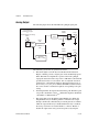
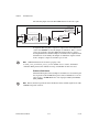
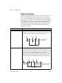
Hardware State Diagram
The following diagram shows the hardware states of the signal generator.
Initiate
Generation
Wait for
Trigger
Idle
Abort
Generation
Started
Event
Abort
Generation
Configure
Done
Event
Done
Event
Hardware
Error
Done
Successful
Completion
Marker and
Data Marker
Events
Abort
Generation
Trigger
Underflow,
PLL Unlocked,
and so on
Started
Event
Generation
Trigger
First Data
Appears
Marker and
Data Marker
Events
The signal generator can be in one of the following six basic states during
the course of operation.
Idle—The device is not generating a waveform. All session properties or
attributes can be programmed in the Idle state. In the Idle state, the
properties or attributes have not necessarily been applied to hardware, so
the hardware configuration of the device may not match the session
property or attribute values. The device remains configured as it was the
last time a session was committed. If the computer has just been powered
on, reset, or the niFgen Reset Device VI or the niFgen_ResetDevice
function has just been called, the device is in the default hardware state.
NI PXIe-5450 User Manual
2-12
ni.com
Chapter 2
NI 5450 Overview
Wait for Trigger—After initiating generation, the device shifts to the Wait
for Trigger state. If the trigger source is immediate, the device immediately
shifts from this state and generates a Started event. If the trigger sources are
configured for a software trigger or for a hardware trigger from one of the
available sources, the device remains in this state until the configured
trigger occurs. When the device recognizes a trigger condition, the device
immediately shifts out of this state and generates a Started event.
First Data Appears—This state is temporary and indicates that waveform
data is just starting to appear at the front panel connector.
Generation—In the Generation state, the device is generating a waveform
as specified by the session attributes configured. Dynamic (or on-the-fly)
properties and attributes, such as the Amplitude, Arbitrary Waveform Gain,
and Arbitrary Waveform Offset properties, or the
NIFGEN_ATTR_FUNC_AMPLITUDE, NIFGEN_ATTR_ARB_GAIN, and the
NIFGEN_ATTR_ARB_OFFSET attributes, are applied immediately to
hardware. Started Event trigger is generated as the device recognizes
triggers. Depending on the configured trigger mode, the device may stay in
the Generation state until the generation is aborted.
Dynamic properties and attributes, such as amplitude, gain, and offset, can
be applied to the device immediately if you set them while the session is in
the Generation state. Refer to the NI-FGEN LabVIEW Reference or the
NI-FGEN C Function Reference for information about the specific
property or attribute that you want to set during generation.
Done—The device has completed the waveform generation as configured
for this session. This state only occurs at the end of a generation state
configured for the Single trigger mode. The device remains in this state
until the you use NI-FGEN to abort the waveform generation and to return
the device to the Idle state.
Hardware Error—An internal hardware error occurred, such as data
underflow, the PLL became unlocked, the device shut down due to an
over-temperature condition, and so on. The signal generator may still be
generating and may be unpredictable at this point. When the driver software
checks the status of the device, an error is returned.
© National Instruments Corporation
2-13
NI PXIe-5450 User Manual
Chapter 2
NI 5450 Overview
Analog Output
The following figure shows the NI 5450 Analog Output signal path.
from Waveform
Generation Engine
or
Onboard Signal Processing
Block
Output
Enable
Lowpass
Filter
16
50 Ω
Direct
Path
Digital
Gain
CH 0 +
Output Enable
Relay
DAC
Direct
Path
Output
Enable
CH 0 -
Lowpass
Filter
Gain DAC
(0 dB to –3 dB)
50 Ω
Output Enable
Relay
NI 5450 analog waveforms are generated as follows:
NI PXIe-5450 User Manual
1.
The 16-bit digital waveform data from the Waveform Generation
Engine or OSP is passed to a digital gain circuit and then high-speed
DAC. This DAC also implements a portion of the Analog Output
signal path attenuation with a range of 0 to 3 dB. Refer to the NI 5450
specifications for the exact resolution. You can adjust the amount of
attenuation by configuring the Arbitrary Waveform Gain property or
the NIFGEN_ATTR_ARB_GAIN attribute. NI-FGEN calculates and sets
the correct amount of attenuation required, corresponding to the gain
setting.
2.
Following the DAC, the signal follows the Direct path. The Direct path
can provide a maximum of 1.0 Vpk-pk differential output into 50 Ω with
a maximum of 3 dB attenuation.
3.
The signal then passes through the Output Enable relay. When the
Output Enable relay is disabled, ground is connected to the output
through a 50 Ω resistor. Intentionally, waveform generation continues
while the output enable relay is disabled. When the relay is enabled,
the analog waveform is seen at the CH 0 +/− connector. Enable or
disable the output of the analog waveform generator by using the
2-14
ni.com
Chapter 2
NI 5450 Overview
niFgen Output Enable VI or the
niFgen_ConfigureOutputEnabled function.
4.
The signal then passes to the differential channel connector. You can
configure the output impedance of the analog waveform generator by
using the niFgen Configure Output Impedance VI or the
niFgen_ConfigureOutputImpedance function.
The NI 5450 uses mechanical relays to switch between the optional paths and
sections in the Analog Output path. When you change a setting that results in a relay
switch, the bouncing of electromechanical relays on the NI 5450 distorts the output signal
for about 10 ms.
Note
Waveform Amplitude Control
The NI 5450 can be configured to achieve required amplitude settings.
Output Paths and Amplifiers
The following figure shows the Direct path.
from Waveform
Generation Engine
or
Onboard Signal Processing
Block
Output
Enable
Lowpass
Filter
16
50 Ω
Direct
Path
Digital
Gain
CH 0 +
Output Enable
Relay
DAC
Direct
Path
Output
Enable
CH 0 -
Lowpass
Filter
Gain DAC
(0 dB to –3 dB)
50 Ω
Output Enable
Relay
The Direct path provides the output of the main DAC to the CH 0+/−
connectors with the fewest electronic components in the path. There are no
programmable amplifiers and there is no method for adding DC offset to
the waveform. The Direct path can generate a maximum of 1.0 Vpk-pk at the
© National Instruments Corporation
2-15
NI PXIe-5450 User Manual
Chapter 2
NI 5450 Overview
CH 0+/− output into matched load impedance. The maximum gain setting
for an Analog Output path configured to the Direct path is 0.5 (gain is a
unitless value).
Attenuation
The main DAC output can be fine-tuned for attenuation, which provides
0 to 3 dB of the Analog Output path signal attenuation. Attenuating the
DAC output signal allows you to vary the signal amplitude while
maintaining the dynamic range of the DAC. You do not lose any bits from
the digital representation of the signal and you do not sacrifice dynamic
range, as you would if you control amplitude by using smaller data ranges
of the DAC. The main DAC also provides the fine resolution for the
attenuation settings.
Fine-tuning of the main DAC attenuation is performed by the gain DAC.
Adjust the gain DAC using the Gain DAC Value property or the
NIFGEN_ATTR_GAIN_DAC_VALUE attribute.
Analog Gain Settings
The following table summarizes the maximum and minimum gain setting
that you can apply for the NI-FGEN Analog path options. Refer to the
device specifications for more information about gain resolution.
Analog Path Gain Summary (Matched Load Impedance)
NI-FGEN Analog Path
Maximum
Gain Value
Minimum
Gain Value
Direct Path without flatness correction
0.5
0.354
Direct Path with flatness correction
0.4
0.284
Note: Gain is unitless.
Digital gain is applied to the digital data before the data is passed to the DAC.
Because relays are not used, digital gain allows glitch-free gain control at the expense of
dynamic range.
Note
NI PXIe-5450 User Manual
2-16
ni.com
Chapter 2
NI 5450 Overview
Digital Gain
Digital gain multiplies waveform data by a factor you specify in the Digital
Gain property or the NIFGEN_ATTR_DIGITAL_GAIN attribute before
converting the data to an analog signal in the DAC. Digital gain can be
changed during generation without the glitches caused by relay switching
that are common when changing analog gains. However, the output
resolution of the DAC is a function of digital gain, meaning that only
analog gain makes full use of the resolution of the DAC.
Flatness Correction
The NI 5450 can use flatness correction to ensure a consistent power level
when generating arbitrary waveforms at any frequency. Flatness correction
is disabled by default in NI-FGEN. You can enable or disable flatness
correction by calling the Flatness Correction Enabled property or the
NIFGEN_ATTR_FLATNESS_CORRECTION_ENABLED attribute.
During external calibration, the frequency response of the Analog path in
its different configurations is measured using the niFgen Initialize Flatness
Calibration VI or the niFgen_InitializeFlatnessCalibration
function and the niFgen Cal Adjust Flatness VI or the
niFgen_CalAdjustFlatness function.
During generation, these measured values are used to compensate for any
attenuation at the requested sample rate. The compensation is applied by a
flatness-correcting FIR filter. This FIR filter applies attenuation to higher
power frequencies so that they become equal to the attenuated frequencies.
As a result, the maximum output voltage is 1.0 Vpk-pk into a 50 Ω load.
Filtering Effects
The delay from the time at which the device receives a trigger to the time
at which the analog output signal is generated increases if the digital and/or
analog filters in the Analog Output path are enabled. In the case of digital
filtering, delay also increases with increase in interpolation. Enabling the
onboard signal processing block can also introduce delay.
The digital filter for the signal generator is inside the FPGA, before the Analog
Output path.
Note
© National Instruments Corporation
2-17
NI PXIe-5450 User Manual
Chapter 2
NI 5450 Overview
Output Enable
You can disable the analog output signal at the differential channel
connectors by controlling the output enable relay, as shown in the
following figure.
CH 0 +
Analog
Output
Path
50 Ω
Output
Enable
CH 0 -
Analog
Output
Path
50 Ω
Output
Enable
*
When the output enable relay is disabled, the output signal is connected to
ground through a 50 Ω resistance. The output enable relay is enabled for
normal waveform generation and connects the differential channel SMA
connectors to the Analog Output path. You can change the output enable
state at any time during waveform generation, and generation continues
internally.
You can enable the output by calling the niFgen Output Enable VI or the
niFgen_ConfigureOutputEnabled function.
The signal generator uses mechanical relays to switch between the output enable
states. When you change a setting that causes a relay to switch, electromechanical relay
bouncing interrupts the output signal for up to 10 ms.
Note
NI PXIe-5450 User Manual
2-18
ni.com
Chapter 2
NI 5450 Overview
Multichannel Configuration
The NI 5450 has two channels that can be configured as active by calling
the niFgen Configure Channels VI or the niFgen_ConfigureChannels
function with a string containing the channel(s) that you wish to activate.
You must configure the channels immediately after calling the niFgen
Initialize VI or the niFgen_init function. The niFgen Configure
Channels VI or the niFgen_ConfigureChannels function cannot be
called after the session has been committed. If a channel is inactive, it will
maintain its output voltage and state until it is made active again or until the
device is reset.
The NI 5450 has two memory banks, one for each channel. When the
niFgen Configure Channels VI or the niFgen_ConfigureChannels
function is called to configure only one channel as active, both channel
memory banks will be configured. This allows you to use the entire
onboard memory for one channel of generation.
Configuring Channels for OSP
The NI 5450 supports one channel of real or complex baseband OSP
generation. When the OSP is enabled, only one channel may be configured
as active. Individual OSP properties can be configured using the I and
Q channel strings (“I” and “Q”, respectively).
Multichannel Waveform Allocation
A waveform consists of all of the data to be generated on all active channels
of a device. A waveform is allocated on a per–device basis, and when
waveform allocation occurs, space is allocated on the device onboard
memory for each channel. Waveform data must therefore be the same size
for each channel.
Because waveforms contain data for all channels, you can only generate
one script, sequence, or arbitrary waveform at a time for all active channels
of the device; you cannot generate separate scripts, sequences, or arbitrary
waveforms on different channels at the same time.
Writing Data
On the NI 5450, data can either be written to channel 0 and
1 independently, to I and Q independently, or to both
channels simultaneously.
© National Instruments Corporation
2-19
NI PXIe-5450 User Manual
Chapter 2
NI 5450 Overview
The flexibility to write waveform data to channels either separately or simultaneously
is especially useful when configuring applications for I/Q generation.
Tip
To write waveform data to an individual channel, begin by allocating space
for waveform data by calling the niFgen Allocate Waveform or niFgen
Allocate Named Waveform VI or the niFgen_AllocateWaveform or
niFgen_AllocateNamedWaveform function. Once you have allocated
the waveform data, call the appropriate niFgen Write Waveform (poly) VI
or one of the niFgen Write Waveform functions with the Channel Name
parameter set to “0” or “1” and the Waveform Name or waveformHandle
parameter set to the name of the waveform previously allocated. You can
repeat these steps to write waveform data to another channel.
To write waveform data to both channels at once, you must first interleave
the data. Once the data is interleaved, call the niFgen Write Waveform
(poly) VI or one of the niFgen Write Waveform functions with the Channel
parameter set to “0,1”.
Interleaved Waveform Data
In order to write data to multiple channels on the same device
simultaneously, the data must be interleaved.
Interleaved samples prioritize samples before channels, such that the array
lists the first sample from every channel in the task, then the second sample
from every channel, up to the last sample from every channel.
When interleaved waveform data is allocated, one sample includes data on multiple
channels. Therefore, the allocation size of interleaved data, in bytes, is equal to (number of
channels being used) × (the number of samples on each channel) × 2.
Note
Channel 0—Sample 1
Channel 1—Sample 1
Channel 0—Sample 2
Channel 1—Sample 2
...
Channel 0—Sample N
Channel 1—Sample N
NI PXIe-5450 User Manual
2-20
ni.com
Chapter 2
NI 5450 Overview
Onboard Signal Processing (OSP)
The onboard signal processing (OSP) block is a general-purpose block of
digital signal processing components that can be used to modify the data
pulled from waveform memory during generation.
The OSP block can be used for the following common applications:
•
Arbitrary Waveform Generation
•
Baseband Interpolation
•
Baseband I/Q Interpolation
Onboard Signal Processing Components
The following figure shows the block diagram of the OSP block.
Onboard Signal Processing
Pre-Filter
Gain I
Waveform
Memory
Output
Engine
Pre-Filter
Offset I
Filtering
and Interpolation I
Digital
Gain I
DAC I
Digital
Gain Q
DAC Q
Frequency
Shift
I/Q
Rate
Pre-Filter
Gain Q
Pre-Filter
Offset Q
Filtering
and Interpolation Q
Programmable I/Q
Gain & Offset Control
Pulse Shaping
and Interpolation
The OSP block includes the following components:
•
Prefilter Gain and Prefilter Offset
•
FIR filters
•
Filtering and Interpolation
•
Writing I/Q Data
© National Instruments Corporation
2-21
NI PXIe-5450 User Manual
Chapter 2
NI 5450 Overview
I/Q Rate
The I/Q rate component holds off the data from the output engine so that a
new sample is only returned once every Total_OSP_Interpolation Sample
clocks.
The Total_OSP_Interpolation is the amount of interpolation applied within the
Filtering and Interpolation component, and does not include the DAC interpolation.
Note
Prefilter Gain
Prefilter gain can change the gain of the I and Q stream during signal
generation. You can change the I and Q prefilter gains independently by
setting the Pre-Filter Gain I and Pre-Filter Gain Q properties or the
NIFGEN_ATTR_OSP_PRE_FILTER_GAIN_I and
NIFGEN_ATTR_OSP_PRE_FILTER_GAIN_Q attributes. The gain can range
from –16.0 to +16.0 (unitless). Any time the prefilter gain changes, the
OSP block ignores all overflows for the next I/Q samples. If an overflow
occurs during these samples, the data is clipped but an error is not returned.
The prefilter gain can be used to attenuate the I/Q data to eliminate
overflows in later stages of the OSP block.
Prefilter Gain Overflow
Any time the following condition is not true for the I or Q data stream, an
overflow occurs when prefilter gain is applied:
–1
≤ User Data × Prefilter Gain ≤ 1
If an overflow occurs, the data is clipped and NI-FGEN returns an error. To
prevent data clipping, attenuate the waveform data or reduce the prefilter
gain.
To disable error reporting caused by OSP overflows, use the OSP Overflow Error
Reporting property or the NIFGEN_ATTR_OSP_OVERFLOW_ERROR_REPORTING attribute.
Tip
Prefilter Offset
Prefilter offset can add offset to the I and Q stream during signal
generation. Change the I and Q prefilter offsets independently by setting
the Pre-Filter Offset I and Pre-Filter Offset Q properties or the
NIFGEN_ATTR_OSP_PRE_FILTER_OFFSET_I and
NIFGEN_ATTR_OSP_PRE_FILTER_OFFSET_Q attributes. The offset can
NI PXIe-5450 User Manual
2-22
ni.com
Chapter 2
NI 5450 Overview
range from negative full scale (−1) to positive full scale (+1). Any time the
prefilter offset changes, the OSP block ignores all overflows for the next
I/Q samples. If an overflow occurs during these samples, the data is clipped
but an error is not returned.
Prefilter Offset Overflow
Any time the following condition is not true for the I or Q data stream, an
overflow occurs when prefilter offset is applied:
–1
≤ (User Data × Pre-Filter Gain) + Pre-Filter Offset ≤ 1
If an overflow occurs, the data is clipped and NI-FGEN returns an error. To
prevent data clipping, reduce the prefilter gain, attenuate the waveform
data, or reduce the prefilter offset.
To disable error reporting caused by OSP overflows, use the OSP Overflow Error
Reporting property or the NIFGEN_ATTR_OSP_OVERFLOW_ERROR_REPORTING attribute.
Tip
FIR Filter Types
There are a number of built-in low-pass pulse-shaping filters available in
NI-FGEN. Because the coefficients are scaled for unity-gain, the filters
may overflow if transients (such as step response) are presented at the input
of the filter. Use the Filter Type property or the
NIFGEN_ATTR_OSP_FIR_FILTER_TYPE attribute to set the FIR filter
type. The following filters are currently available:
Note
•
Flat
•
Raised Cosine
•
Root Raised Cosine
Enabling filters in the OSP will add a constant group delay to your signal.
Digital Filter Overflow
FIR filters may overflow. If an overflow occurs, data is clipped and
NI-FGEN returns an error.
Digital filter overflows are caused by transients. Transients can occur as an
abrupt jump at the beginning of a waveform or they may be present in the
data you supply. NI-FGEN ignores overflows that are caused by transients
at the beginning of a waveform. You can choose to ignore overflow errors
caused by transients present in your data with the OSP Overflow Error
Reporting property or the
NIFGEN_ATTR_OSP_OVERFLOW_ERROR_REPORTING attribute.
© National Instruments Corporation
2-23
NI PXIe-5450 User Manual
Chapter 2
NI 5450 Overview
FIR Filter Type: Flat
Passband Value: 0.40
This lowpass filter is designed to give a flat response until the passband
value. The passband value is a fraction of the I/Q Rate coming into the FIR
filter. Use the Flat Filter Passband property or the
NIFGEN_ATTR_OSP_FIR_FILTER_FLAT_PASSBAND attribute to set the
passband value.
The Flat filter stopband does not begin until 0.6 × I/Q Rate. If you provide data
that has frequency content above 0.4 × I/Q Rate, then aliasing occurs in the output
spectrum. NI recommends you keep all frequency content below 0.4 × I/Q Rate when using
the Flat filter.
Caution
The following diagram shows the Flat Filter response with a passband of
0.4. The frequency axis is scaled as a fraction of the I/Q Rate.
10 –
0–
–10 –
Magnitude (dB)
–20 –
–30 –
–40 –
–50 –
–60 –
–70 –
–80 –
NI PXIe-5450 User Manual
–
–
–
–
0.3
–
0.2
–
–
0.1
–
–
–
–100 –
0
–
–90 –
0.4
0.5
0.6
Frequency (Hz)
0.7
0.8
0.9
1
2-24
ni.com
Chapter 2
NI 5450 Overview
FIR Filter Type: Raised Cosine
Alpha Values: 0.1 to 0.4
This lowpass filter is commonly used in communications applications. The
passband of the raised cosine filter stops at 0.5 × (1 − α) of the I/Q Rate.
The stopband of the raised cosine filter begins at 0.5 × (1 + α) of the I/Q
Rate. The transition-band of the raised cosine filter (in dB) follows the
following formula:
where
S is 0.5 × (1 − α)
f is Frequency (fraction of the I/Q Rate)
Use the Raised Cosine Filter Alpha property or the
NIFGEN_ATTR_OSP_FIR_FILTER_RAISED_COSINE_ALPHA attribute to
set the α value.
The following diagram shows an ideal raised cosine filter response with an
α of 0.5. The frequency axis is scaled as a fraction of the I/Q Rate.
0–
–10 –
–20 –
Amplitude (dB)
–30 –
–40 –
–50 –
–60 –
–70 –
–80 –
© National Instruments Corporation
–
–
0.8
–
0.6
–
–
0.4
–
–
0.2
–
–
–
–100 –
0
–
–90 –
1
1.2
Frequency
1.4
1.6
1.8
2
2-25
NI PXIe-5450 User Manual
Chapter 2
NI 5450 Overview
FIR Filter Type: Root Raised Cosine
Alpha Values: 0.1 to 0.4
This lowpass filter is commonly used in communications applications. The
passband of the root raised cosine filter stops at 0.5 × (1 − α) of the I/Q
Rate. The stopband of the root raised cosine filter begins at
0.5 × (1 + α) of the I/Q Rate. The transition-band of the root raised cosine
filter (in dB) follows the following formula:
where
S is 0.5 × (1 − α)
f is Frequency (fraction of the I/Q Rate)
Use the Raised Cosine Filter Alpha property or the
NIFGEN_ATTR_OSP_FIR_FILTER_RAISED_COSINE_ALPHA attribute to
set the α value.
The following diagram shows an ideal root raised cosine filter response
with an α of 0.5. The frequency axis is scaled as a fraction of the I/Q Rate.
0–
–10 –
–20 –
Amplitude (dB)
–30 –
–40 –
–50 –
–60 –
–70 –
–80 –
NI PXIe-5450 User Manual
–
–
0.8
–
0.6
–
–
0.4
–
–
0.2
–
–
–
–100 –
0
–
–90 –
1
1.2
Frequency
1.4
1.6
1.8
2
2-26
ni.com
Chapter 2
NI 5450 Overview
Filtering and Interpolation
The filtering and interpolation stage of the OSP block increases the
effective sample rate of the signal generator while protecting the frequency
spectrum of the interpolated data from images. This protection occurs when
the data passes through a lowpass filter after zero stuffing. The frequency
response of the low pass filter can be changed with the Filter Type property
or the NIFGEN_ATTR_OSP_FIR_FILTER_TYPE attribute.
Input Data
Zero
Stuff
Low Sample Rate
Low Pass
Filter
Output Data
High Sample Rate
Writing I/Q Data
On multichannel devices, I/Q data can either be written to individual
channels (for example, designating one channel for I data and one channel
for Q data) or to both channels of the device at once when following the
multichannel waveform allocation guidelines.
Basic Onboard Signal Processing Properties
The following properties must be configured before you can use the OSP
block:
•
OSP Mode
•
OSP Enabled
•
Data Processing Mode
•
IQ Rate
•
Frequency Shift
•
FIR Filter Type
OSP Mode
The OSP Mode property or the NIFGEN_ATTR_OSP_MODE attribute
specifies the generation mode implemented by the OSP block. The OSP
block can operate in IF and Baseband modes. On the NI 5450, the default
OSP mode is Baseband generation.
© National Instruments Corporation
2-27
NI PXIe-5450 User Manual
Chapter 2
NI 5450 Overview
In baseband mode, I/Q data is filtered, interpolated, and scaled in the device
OSP. The device generates I data at the CH 0+ and CH 0− differential
output terminals and Q data on the CH 1+ and CH 1– differential output
terminals.
OSP Enabled
The OSP Enabled property or the NIFGEN_ATTR_OSP_ENABLED attribute
activates the functionality of the OSP block. To use any of the features in
the OSP block, you must enable onboard signal processing by setting this
property or attribute.
Data Processing Mode
Data Processing mode determines whether the OSP block uses only the
I signal path to generate waveforms or uses the I and Q signal paths to
generate complex waveforms. If the waveform data is configured for real
data points by setting the Data Processing Mode property or the
NIFGEN_ATTR_OSP_DATA_PROCESSING_MODE attribute, only the I signal
path is used. If the Data Processing Mode property is set to Complex or the
NIFGEN_ATTR_OSP_DATA_PROCESSING_MODE attribute is set to
NIFGEN_VAL_OSP_COMPLEX, both the I and Q signal paths are used.
Complex waveform data should be downloaded to the signal generator
using the niFgen Write Waveform Complex VI or the
niFgen_WriteWaveformComplexf64 function.
IQ Rate
The IQ Rate property or the NIFGEN_ATTR_OSP_IQ_RATE attribute
defines the rate at which data is processed by the OSP block. If the
waveform data is configured for real data points by setting the Data
Processing Mode property or the
NIFGEN_ATTR_OSP_DATA_PROCESSING_MODE attribute, then it is the
rate at which each sample from waveform memory is taken from memory
and inserted into the OSP block. If the waveform data is configured for
complex data points by setting the Data Processing Mode property or the
NIFGEN_ATTR_OSP_DATA_PROCESSING_MODE attribute, then it is the
rate at which each complex sample is taken from memory and inserted into
the OSP block.
When the onboard signal processing is enabled by setting the OSP Enabled
property or the NIFGEN_ATTR_OSP_ENABLED attribute, you cannot set the Sample Rate
property or the NIFGEN_ATTR_ARB_SAMPLE_RATE attribute.
Note
NI PXIe-5450 User Manual
2-28
ni.com
Chapter 2
NI 5450 Overview
Using an External Clock with the OSP Block
Some applications may require lower jitter or phase noise than is provided
by the onboard High-Resolution clock. You can use an external clock
source to achieve spectral purity at any arbitrary I/Q rate. To determine the
frequency of the sample rate for the external clock source, complete the
following steps.
1.
Set the Sample Clock Source property or the
NIFGEN_ATTR_SAMPLE_CLOCK_SOURCE attribute to the external
clock source you are using.
2.
3.
Set the IQ Rate property or the NIFGEN_ATTR_OSP_IQ_RATE
attribute.
Read the value of the Sample Rate property or the
NIFGEN_ATTR_ARB_SAMPLE_RATE attribute.
4.
Set the external clock source sample rate to the frequency of the
Sample Rate property or the NIFGEN_ATTR_ARB_SAMPLE_RATE
attribute that you just read.
5.
Validate that the external Sample clock source is connected to the
NI 5450 connector specified in the Sample Clock Source property or
the NIFGEN_ATTR_SAMPLE_CLOCK_SOURCE attribute and is
generating a clock before you continue configuring the NI 5450.
For more information about using external clocks, refer to External Sample
Clock Sources.
Frequency Shift
The Frequency Shift property or the
NIFGEN_ATTR_OSP_FREQUENCY_SHIFT attribute can be used to shift the
frequency of a baseband signal. This property can only be used when the
OSP mode has been configured for baseband by setting the OSP Mode
property or the NIFGEN_ATTR_OSP_MODE attribute.
When you are using the NI 5450 with an external I/Q modulator, the
Frequency Shift property or the NIFGEN_ATTR_OSP_FREQUENCY_SHIFT
attribute modifies the baseband I/Q data such that the resulting RF signal is
shifted in frequency.
When the NI 5450 is configured for single-channel operation in Real data processing
mode, you can use the active baseband channel as a direct, frequency-shifted output, in
addition to creating RF frequency shifts with an I/Q modulator.
Note
© National Instruments Corporation
2-29
NI PXIe-5450 User Manual
Chapter 2
NI 5450 Overview
FIR Filter Type
Use the FIR Filter Type property or the
NIFGEN_ATTR_OSP_FIR_FILTER_TYPE attribute to set the FIR filter
type. The following filter types are supported:
•
Flat
•
Raised Cosine
•
Root Raised Cosine
Common Onboard Signal Processing Applications
The OSP block is particularly useful for the following common
applications:
•
Arbitrary Waveform Generation
•
Baseband Interpolation
•
Baseband I/Q Interpolation
Arbitrary Waveform Generation
The following figure shows the behavior of the OSP block during arbitrary
waveform generation.
Waveform
Memory
Digital
Gain
Output
Engine
DAC
Onboard Signal Processing
For normal arbitrary waveform generation, disable onboard signal
processing by setting the OSP Enabled property or the
NIFGEN_ATTR_OSP_ENABLED attribute.
NI PXIe-5450 User Manual
2-30
ni.com
Chapter 2
NI 5450 Overview
Baseband Interpolation
The following figure shows the behavior of the OSP block during baseband
interpolation.
Onboard Signal Processing
Pre-Filter
Gain I
Waveform
Memory
Output
Engine
Pre-Filter
Offset I
Digital
Gain I
Filtering
and Interpolation I
DAC I
Frequency
Shift
I/Q
Rate
Baseband interpolation allows the OSP block to interpolate signals at a low
sample rate up to a high sample rate. Arbitrary pulse shaping of the data can
also be done in the FIR filter. For baseband interpolation, complete the
following steps.
1.
Enable onboard signal processing by setting the OSP Enabled property
or the NIFGEN_ATTR_OSP_ENABLED attribute.
2.
Specify the use of real numbers for the waveform data by setting the
Data Processing Mode property or the
NIFGEN_ATTR_OSP_DATA_PROCESSING_MODE attribute.
3.
Set the IQ Rate property or the NIFGEN_ATTR_OSP_IQ_RATE
attribute to the low sample rate of the waveform data.
4.
Set the FIR Filter Type property or the
NIFGEN_ATTR_OSP_FIR_FILTER_TYPE attribute.
5.
6.
Set the corresponding filter parameter.
Disable the carrier by setting the Carrier Enabled property or the
NIFGEN_ATTR_OSP_CARRIER_ENABLED attribute.
7.
© National Instruments Corporation
Download the low sample rate waveform(s) to the signal generator.
2-31
NI PXIe-5450 User Manual
Chapter 2
NI 5450 Overview
Baseband I/Q Interpolation
The following figure shows the behavior of the OSP block during baseband
I/Q interpolation.
Onboard Signal Processing
Pre-Filter
Gain I
Waveform
Memory
Output
Engine
Pre-Filter
Offset I
Filtering
and Interpolation I
Digital
Gain I
DAC I
Digital
Gain Q
DAC Q
Frequency
Shift
I/Q
Rate
Pre-Filter
Gain Q
Pre-Filter
Offset Q
Filtering
and Interpolation Q
Programmable I/Q
Gain & Offset Control
Pulse Shaping
and Interpolation
Baseband I/Q interpolation allows the OSP block to interpolate complex
data signals at a low sample rate up to a high sample rate. Arbitrary pulse
shaping of the data can also be done in the FIR filter. For baseband I/Q
interpolation, complete the following steps.
1.
Enable onboard signal processing by setting the OSP Enabled property
or the NIFGEN_ATTR_OSP_ENABLED attribute.
2.
Set the OSP mode to Baseband by calling the OSP Mode property or
the NIFGEN_ATTR_OSP_MODE attribute
3.
Specify the use of complex numbers for the waveform data by setting
the Data Processing Mode property or the
NIFGEN_ATTR_OSP_DATA_PROCESSING_MODE attribute.
4.
Set the IQ Rate property or the NIFGEN_ATTR_OSP_IQ_RATE
attribute to the low sample rate of the waveform data.
5.
Set the FIR Filter Type property or the
NIFGEN_ATTR_OSP_FIR_FILTER_TYPE attribute.
6.
Set the corresponding filter parameter.
7.
(Optional) Shift the frequency by calling the Frequency Shift property
or the NIFGEN_ATTR_OSP_FREQUENCY_SHIFT attribute.
8.
Download the low sample rate waveform(s) to the signal generator.
9.
Read the sample rate by calling the Sample Rate property or the
NIFGEN_ATTR_ARB_SAMPLE_RATE attribute.
NI PXIe-5450 User Manual
2-32
ni.com
Chapter 2
NI 5450 Overview
Baseband Interpolation Considerations
The NI 5450 implements baseband interpolation in order to reduce the
power of aliased images. Interpolation is a process that effectively turns a
lower sample rate into a higher sample rate. Because the signal is now at a
higher sample rate, images are moved to higher frequencies, where they fall
in the rejection band of the image rejection filter and are suppressed.
NI-FGEN automatically selects the largest interpolation factor to achieve
the maximum possible DAC sample rate. The interpolated sample rate can
then be read with the Sample Rate property or the
NIFGEN_ATTR_ARB_SAMPLE_RATE attribute.
For optimum performance, National Instruments recommends maintaining the
sample rate between 270 MS/s and 400 MS/s due to the fixed frequency characteristics of
the image rejection filter. For more information about the image rejection filter, refer to the
NI 5450 specifications.
Note
Interpolation Settings
To determine the total interpolation and interpolated sample rate, divide
400 MS/s by your desired sample rate and round down to the nearest step,
as noted in the Interpolation table for your total interpolation value. Then,
consult the following table for settings that will allow you to achieve your
desired interpolated sample rate.
With OSP enabled, Desired Sample Rate (Data Rate) = Symbol Rate ×
Samples/Symbol.
Note
Example: At a desired sample rate of 4.5 MS/s, the total interpolation will
be determined by the following calculations:
400 MS/s ÷ 4.45 MS/s = 89.88× total interpolation
A total interpolation rate of 89.88× falls in the 24-8192 Total Interpolation
range in the Interpolation table. As this range is measured in steps of 8, you
must round down to the nearest multiple of 8, yielding a total interpolation
rate of 88×. This value corresponds to a sample rate of 391.6 MS/s and a
worst case image at or below –100 dB.
© National Instruments Corporation
2-33
NI PXIe-5450 User Manual
Chapter 2
NI 5450 Overview
Interpolated
Sample
Rate*
(MS/s)
Theoretical
Worst Case
Image
Feedthrough
(dB),
20 MS/s
Bandwidth
Signal
Theoretical
Worst Case
Image
Feedthrough†
(dB),
Maximum
I/Q
Bandwidth
Desired Sample
Rate (S/s)
I/Q
Bandwidth
(Hz)
1 Sample
/symbol
12 to 24 k
4.8 to 9.6 k
16384 to 32768
in steps of 32
370 to 400
N/A
<–100
24 to 48 k
9.6 to 19.2 k
8192 to 16384
in steps of 16
370 to 400
N/A
<–100
48k to 16.66 M
19.2 k to
6.664 M
24 to 8192
in steps of 8
310 to 400
N/A
–100
16.66 to 33.33 M
6.664 to
13.332 M
12 to 24
in steps of 4
300 to 400
N/A
–88
33.33 to 50 M
13.332 to 20 M
8
267 to 400
N/A
–61
50 to 67.5 M
20 to 27 M
4
200 to 270
–31
–23
67.5 to 100 M
27 to 40 M
4
270 to 400
–62
–45
100 to 135 M
40 to 54 M
2
200 to 270
–31
–31
135 to 200 M
54 to 80 M
2
270 to 400
–62
–28
200 to 270 M
80 to 108 M
1
200 to 270
–31
–8
270 to 399 M
108 to 159.6 M
1
270 to 399
–62
–8
400 M
120 M
1
400
–82
–52
Total
Interpolation
Assumptions: Internal Sample clock, High Resolution clock mode. Desired sample rate ranges do not include the first point
(a desired sample rate of 50 MS/s yields 8x total interpolation).
* If your interpolated sample rate falls within an undesirable band, you can use the Modulation Toolkit to provide fractional
resampling that will adjust the sample rate to achieve better image rejection.
† Calculated from sinc response and typical filter rejection for the NI 5450. Refer to the NI 5450 specifications for more
information about the expected performance of the NI 5450.
NI PXIe-5450 User Manual
2-34
ni.com
Chapter 2
NI 5450 Overview
Clock Source and Frequency
The NI 5450 has a Sample clock rate of 12.2 kHz to 400 MHz. The timing
of the device is very flexible, and you have multiple choices for deriving
the Sample clock. There are modes for deriving the Sample clock from the
internal Sample clock timebase, as well as modes to provide external
clocks. You also have several choices for providing the frequency
reference for the onboard phase-locked loop.
Reference Clock
Divide/M
Sample Clock
Timebase/M
CLK OUT
Divide/K
External Sample Clock
CLK IN
PLL
PXI_CLK10
High
Resolution
Oscillator
CH 0
Channel Sample Clock
Delay
PLL* W
with Phase
Adjust
Sample
Clock
Timebase
(None)
Divide/N
CH 1
Channel Sample Clock
Delay
External Sample Clock Timebase
Clocking Options
Waveform generation is driven by the Sample clock; depending on your
application, some sources may be better choices than others. You can use
the following sources for the NI 5450 Sample clock:
•
Internal Sample clock—the onboard clock is used as the Sample clock
source and the Sample clock is derived from the Sample clock
timebase.
•
External Sample clock—the Sample clock has an external source that
derives device clocking by directly driving the DAC and all waveform
generation operations on the device.
•
Reference clock—the Sample clock is derived from an external source
that is phase–locked to the Sample clock timebase. The phase-locked
loop (PLL) Reference clock source specifies the source of the control
voltage that tunes the VCXO of the Sample clock timebase for internal
clock update sources. The PLL circuit adjusts the Sample clock
timebase VCXO to synchronize to a Reference clock. The frequency
stability of the Sample clock timebase matches that of the PLL
Reference clock when the two are phase-locked. Phase-locking also
synchronizes multiple device clocks that are phase–locked to the same
Reference clock.
© National Instruments Corporation
2-35
NI PXIe-5450 User Manual
Chapter 2
NI 5450 Overview
•
External Sample clock timebase—the Sample clock timebase has an
external source that derives device clocking by directly driving the
DAC and all waveform generation operations on the device.
The following table shows the valid NI-FGEN property or attribute value
combinations that can be used to configure the clock settings for an internal
Sample clock, an external Sample clock, or a Reference clock. The term
Update clock is synonymous with Sample clock.
Sample Clock
Source*
Clock Mode*
“OnboardClk”
(default)
NIFGEN_VAL_HIGH_
RESOLUTION
PLL Reference
Clock Source*
“None” (default)
“PXI_CLK10”
“ClkIn”
NIFGEN_VAL_
AUTOMATIC (default)
“None” (default)
“PXI_CLK10”
“ClkIn”
“ClkIn”
Not Applicable
Not Applicable
* These column headings refer to NI-FGEN properties. The attributes that correspond to
these properties are NIFGEN_ATTR_SAMPLE_CLOCK_SOURCE,
NIFGEN_ATTR_CLOCK_MODE, and NIFGEN_ATTR_REFERENCE_CLOCK_SOURCE. The
values in the columns represent the values that can be set on these properties or attributes.
Settings that line up horizontally show valid combinations of the NI-FGEN settings.
NI PXIe-5450 User Manual
2-36
ni.com
Chapter 2
NI 5450 Overview
Internal Sample Clock
The NI 5450 can derive a Sample clock from its main internal timing
source—the Sample clock timebase. The signal generator provides a
high-precision 400 MHz oscillator clock source for the Sample clock
timebase.
The following figure shows the NI 5450 internal Sample clock Source path.
Reference Clock
Divide/M
Sample Clock
Timebase/M
CLK OUT
Divide/K
External Sample Clock
CLK IN
PLL
PXI_CLK10
High
Resolution
Oscillator
CH 0
Channel Sample Clock
Delay
PLL* W
with Phase
Adjust
Sample
Clock
Timebase
(None)
Divide/N
CH 1
Channel Sample Clock
Delay
External Sample Clock Timebase
The NI 5450 has a high-resolution internal clock. You can change the
frequency of this clock by calling the niFgen Set Sample Rate VI or the
niFgen_ConfigureSampleRate function. When you set a desired
sample rate, NI-FGEN will internally determine and apply appropriate
divide-down factors.
The jitter of the High-Resolution clocking mode is frequency–dependent. At low
frequencies the jitter increases. Refer to the device specifications for more information
about jitter.
Note
Phase-Locked Loop Reference Clock
A phase-locked loop (PLL) is a circuit that tunes the Sample clock timebase
to phase–lock to an external Reference clock. The PLL Reference clock
source controls the source of the control voltage that tunes the VCXO of
the Sample clock timebase for internal clock update sources. The frequency
stability and accuracy of the Sample clock timebase matches that of the
Reference clock when they are phase–locked. Using the PLL on your
device enables you to frequency-lock multiple devices in a single chassis
or devices in separate chassis.
Refer to the device specifications for information about the PLL reference
frequencies available on your device.
Note
© National Instruments Corporation
2-37
NI PXIe-5450 User Manual
Chapter 2
NI 5450 Overview
The following figure shows the NI 5450 Reference Clock Source path.
Reference Clock
Divide/M
Sample Clock
Timebase/M
CLK OUT
Divide/K
External Sample Clock
CLK IN
PLL
PXI_CLK10
High
Resolution
Oscillator
CH 0
Channel Sample Clock
Delay
PLL* W
with Phase
Adjust
Sample
Clock
Timebase
(None)
Divide/N
CH 1
Channel Sample Clock
Delay
External Sample Clock Timebase
To begin the PLL, the phase comparator compares the selected Reference
clock to the 400 MHz clock of the Sample clock timebase. Next, a control
voltage proportional to the phase difference between the two clocks is
developed and used to tune the Sample clock timebase into alignment with
the Reference clock. Finally, the Sample clock timebase output is routed
back to the phase comparator, and the loop is closed.
Note When the Reference Clock Source property or the
NIFGEN_ATTR_REFERENCE_CLOCK_SOURCE attribute is set to “None”; the internal
calibration DAC generates the calibration voltage, and the PLL circuit is not used.
Reference Clock Sources
The NI 5450 can phase-lock its Sample clock timebase to an external signal
that is present on the CLK IN front panel connector. PXI devices can also
phase–lock to a 10 MHz Reference clock signal provided by the PXI bus
(PXI_CLK10).
Refer to the device specifications for information about available signal levels on the
CLK IN front panel connector.
Note
NI PXIe-5450 User Manual
2-38
ni.com
Chapter 2
NI 5450 Overview
External Sample Clock Sources
The NI 5450 can accept an external clock to directly drive the Sample
clock. When using an external Sample clock, the frequency stability and
accuracy of the Sample clock is determined by the provided external
Sample clock.
The following figure shows possible Sample Clock paths.
Reference Clock
Divide/M
Sample Clock
Timebase/M
CLK OUT
Divide/K
External Sample Clock
CLK IN
PLL
PXI_CLK10
High
Resolution
Oscillator
CH 0
Channel Sample Clock
Delay
PLL* W
with Phase
Adjust
Sample
Clock
Timebase
(None)
Divide/N
CH 1
Channel Sample Clock
Delay
External Sample Clock Timebase
You can set the clock source by calling the niFgen Configure Sample Clock
Source VI or the niFgen_ConfigureSampleClockSource function.
You can multiply the clock by an integer, W (or 1/W) by calling the
External Sample Clock Multiplier property or the
NIFGEN_ATTR_EXTERNAL_SAMPLE_CLOCK_MULTIPLIER attribute.
When using an external Sample clock you should configure the Sample
clock rate by calling the niFgen Set Sample Rate VI or the
niFgen_ConfigureSampleRate function.
Note
Refer to the device specifications for the allowable voltages, signal types, and
clocks that you can use for all external Sample clocks.
© National Instruments Corporation
2-39
NI PXIe-5450 User Manual
Chapter 2
NI 5450 Overview
External Sample Clock Considerations
The NI 5450 incorporates high-speed digital clocking technology and
requires a stable, free-running Sample clock to operate properly. When the
signal generator is committed—either explicitly by calling the niFgen
Commit VI or the niFgen_Commit function or implicitly by writing
waveforms or sequences or initiating a generation—the external Sample
clock must be available to the device. If the external clock becomes
unstable due to glitching, changing frequency, or is removed entirely,
NI-FGEN returns a hardware clocking error.
If necessary, you can change the rate or the source of the external Sample
clock between subsequent generations by first calling the niFgen Abort
Generation VI or the niFgen_AbortGeneration function, changing the
rate or source, and then calling the niFgen Commit VI or the
niFgen_Commit function. NI-FGEN reprograms the NI 5450 for the new
settings, and you can call the niFgen Initiate Generation VI or the
niFgen_InitiateGeneration function to start the next generation.
If you must remove the external Sample clock between generations (after
calling the niFgen Abort Generation VI or niFgen_AbortGeneration
function, but before calling the niFgen Initiate VI or the niFgen_Init
function), but are not changing the frequency or source of the external
clock, you can choose one of the following options:
•
Call the niFgen Initiate VI or the niFgen_Init function, which
returns a hardware clocking error because the external Sample clock is
gone, then clear the error and call the niFgen Initiate VI or the
niFgen_Init function again. NI-FGEN then reprograms the
hardware to use the external clock again.
•
Force the device to be recommitted by changing a property or attribute
to another value and then back to its original value. This action causes
NI-FGEN to re-commit the settings to hardware, which does not
happen otherwise because NI-FGEN does not know that the external
Sample clock is gone.
When configuring an external Sample clock, you can set the sample rate to the
exact frequency you are using to avoid data errors by calling the niFgen Set Sample Rate
VI or the niFgen_ConfigureSampleRate function.
Caution
NI PXIe-5450 User Manual
2-40
ni.com
Chapter 2
NI 5450 Overview
External Sample Clock Timebase
The Sample clock timebase has an external source that derives device
clocking by directly driving the DAC and all waveform generation
operations on the device.
Reference Clock
Divide/M
Sample Clock
Timebase/M
CLK OUT
Divide/K
External Sample Clock
CLK IN
PLL
PXI_CLK10
Resolution
Oscillator
CH 0
Channel Sample Clock
Delay
PLL* W
with Phase
Adjust
Sample
Clock
Timebase
(None)
Divide/N
CH 1
Channel Sample Clock
Delay
External Sample Clock Timebase
You can set the Sample clock timebase source by calling the Sample Clock
Timebase Source property or the
NIFGEN_ATTR_SAMPLE_CLOCK_TIMEBASE_SOURCE attribute. You can
set the Sample clock timebase rate with the Sample Clock Timebase Rate
property or the NIFGEN_ATTR_SAMPLE_CLOCK_TIMEBASE_RATE
attribute.
You can export the Sample clock timebase to a terminal configured by the
Sample Clock Timebase Export Output Terminal property or the
NIFGEN_ATTR_EXPORTED_SAMPLE_CLOCK_TIMEBASE_OUTPUT_
TERMINAL attribute.
Note
Refer to the device specifications for the allowable voltages, signal types, and
clocks that you can use for an external Sample clock timebase.
© National Instruments Corporation
2-41
NI PXIe-5450 User Manual
Chapter 2
NI 5450 Overview
Exporting Clocks
The NI 5450 provides resources for exporting your clocks and multiple
destinations for routing.
Reference Clock
Sample Clock Timebase
Divide/M
Sample Clock
Timebase/M
CLK OUT
Sample Clock/K
Sample Clock
Divide/K
The following table shows the available clock signals that can be routed to
devices external to the signal generator and the destination options.
The PFI outputs have a bandwidth of 200 MHz. The PXI Trigger lines have a
bandwidth of <20 MHz. The following table shows the software limits of the export
destinations.
Note
Clock to be Exported
Destination Options
CLK OUT
PFI<0..1>
PXI_Trig<0..6>
Sample Clock/K
K ≥1
K ≥2
K ≥2
SCTB/M
M ≥1
M ≥2
M ≥2
Always
Always
Always
Reference Clock
Note: All divisors have a default value of 1.
For synchronization purposes, the NI 5450 allows you to export your clocks
so that other devices can share the timing of the NI 5450. The following
sections describe the possible clock routing configurations.
Sample Clock
The Sample clock can be routed to the CLK OUT front panel SMA
connector.
Additionally, the exported clock can be divided down by an integer value
(no less than 2) before being exported to the PFI <0..1> connectors, the
NI PXIe-5450 User Manual
2-42
ni.com
Chapter 2
NI 5450 Overview
CLK OUT connector, or the PXI_Trig<0..6> lines. Refer to the Exported
Sample Clock Divisor property or the
NIFGEN_ATTR_EXPORTED_SAMPLE_CLOCK_DIVISOR attribute for more
information about configuring the Sample clock divisor.
Sample Clock Timebase
The Sample clock timebase can be routed to the CLK OUT front panel
SMA connector.
Additionally, the exported clock can be divided down by an integer value
before being exported to the PFI <0..1> connectors, the CLK OUT
connector, or the PXI_Trig<0..6> lines. You can configure the Sample
clock divisor by calling the Exported Sample Clock Timebase Divisor
property or the
NIFGEN_ATTR_EXPORTED_SAMPLE_CLOCK_TIMEBASE_DIVISOR
attribute.
Reference Clock
The Reference clock is the actual clock that is configured for the signal
generator phase-locked loop circuit to use as a reference. You configure a
Reference clock as a PLL Reference clock source for the signal to be
available for exporting. The Reference clock can be routed to the
PFI <0..1> front panel SMB connectors, the CLK OUT front panel SMA
connector, or the PXI_Trig<0..6> lines on the PXI trigger bus.
NI-FGEN allows values for Reference clock frequency on the NI 5450 from
1 to 100 MHz in 1 MHz increments, 102 to 200 MHz in 2 MHz increments, and 204 to
400 MHz in 4 MHz increments.
Note
Destination Options
The following sections define the destinations for exported clocks.
PFI <0..1>—The Sample clock (when K ≥2), the Sample clock timebase
(when M ≥2), and the Reference clock can be exported to the PFI 0 and
PFI 1 SMB connectors on the front panel to synchronize external devices.
You must configure the device to export the desired clock to the PFI SMB
connectors.
CLK OUT—The Sample clock, the Sample clock timebase, and the
Reference clock can be exported to the CLK OUT SMA connectors on the
front panel to synchronize external devices. You must configure the device
to export the desired clock to the CLK OUT SMA connector.
© National Instruments Corporation
2-43
NI PXIe-5450 User Manual
Chapter 2
NI 5450 Overview
PXI_Trig<0..6>—Sample clock (when K ≥2), the Sample clock timebase
(when M ≥2), and the Reference clock can be exported to the PXI_Trig
lines. The PXI standards allow for devices to route signals to other devices
in your PXI Express chassis to enhance device-to-device synchronization.
Refer to the chassis documentation for specifications to ensure the
reference signal is within tolerance. You must configure the device to
export the desired clock to the PXI_Trig line.
Refer to niFgen Export Signal VI or the niFgen_ExportSignal function
for more information about configuring the destinations for the desired
clock signal.
Onboard Memory
The NI 5450 signal generator uses an onboard memory that is 16-bits wide.
The minimum standard memory size for the NI 5450 is 128 MB. With the
minimum standard memory size, you can store very long waveforms on the
device and obtain reliable waveform generation at full sample rate of
400 MS/s. The NI 5450 also comes with higher memory options of 512 MB
or 2 GB.
The onboard memory is a single large memory area per channel that stores
both waveforms and sequence instructions to generate the waveforms. The
instructions for a complicated sequence can occupy a significant portion of
memory. The architecture of the NI 5450 allows you to load multiple
waveforms and multiple sequence instructions into the memory. The
following diagram illustrates NI 5450 memory allocation. A number of
waveforms are stored in the onboard memory ranging from 1 to n; there are
also a number of sequence instructions ranging in number from 1 to m. The
values of n and m depend on the waveform and instructions configured and
are ultimately limited by the amount of memory.
Waveform
1
Waveform
2
NI PXIe-5450 User Manual
•••
Waveform
n
Sequence
Instructions
1
2-44
Sequence
Instructions
2
•••
Sequence
Instructions
m
Free
Memory
ni.com
Chapter 2
NI 5450 Overview
The following tables list the types of information that are used to make up
the instructions that are saved to memory. You can store the instructions for
multiple sequences to the onboard memory ahead of time and generate
them later, allowing for quick reconfiguration times between tests. There
are two example sequences. Sequence 1 represents the instructions for a
sequence containing a maximum number of segments k. Sequence m is an
example of a sequence containing 8 segments. Each sequence downloads
different waveforms to the onboard memory, and uses various looping and
Marker placement options to construct the resulting waveform.
Sequence 1: Burst Trigger Mode
Sequence Segment
Waveform
Number of Loops
Marker Placement
1
1
1
0
2
5
14
100
3
17
1
–1
4
12
18,045
10,000
5
12
64,000
12
6
34
64,000
0
20
10,000
.........
k
15
Sequence m: Stepped Trigger Mode
Sequence Segment
Waveform
Number of Loops
Marker Placement
1
1
1
0
2
2
340
4
3
35
1
–1
4
2
10
0
5
340
5
10,000
6
34
64,000
0
7
20,000
1,000,000
13
8
1
1
0
© National Instruments Corporation
2-45
NI PXIe-5450 User Manual
Chapter 2
NI 5450 Overview
Onboard Memory for Multichannel
Waveform Generation
On multichannel devices, onboard memory is allocated separately for each
configured channel. When you write a waveform to the onboard memory
of a multichannel device, the space required for the waveform is allocated
in the onboard memory for each channel.
You can write different data to the waveform allocated for each channel, as
long as the data written requires the same amount of memory on each
channel. For example, Waveform 1 can contain a ramp wave on channel 0
and a square wave on channel 1, as shown in the following figure.
Waveform
1
Waveform
2
Waveform
1
Waveform
2
Waveform
3
Waveform
4
Waveform
3
Waveform
4
Free
Memory
Channel 0
Free
Memory
Channel 1
Waveform and Generation Instruction Memory Size
Waveform Memory Size
Waveforms are stored in the NI 5450 onboard memory in contiguous
blocks. These blocks are allocated in multiples of 128 bytes. This allocation
style means that while waveform sizes may be multiples of two samples
(four bytes) on the NI 5450, the amount of onboard memory allocated for
each waveform is a multiple of 128 bytes. The following figure represents
the total memory of a device and shows memory that was initially empty,
but it now has multiple waveforms written to it, nearly filling the device
memory.
NI PXIe-5450 User Manual
2-46
ni.com
Chapter 2
Waveform
1
Waveform
2
•••
Waveform
n
Sequence
Instructions
1
Sequence
Instructions
2
•••
NI 5450 Overview
Sequence
Instructions
m
Free
Memory
Calculate the amount of memory that a waveform takes up in the onboard
memory with the following two rules.
1.
Each sample in the waveform uses two bytes of memory space. Four
bytes are used when the onboard signal processing block is enabled
and the Data Processing Mode property is set to Complex or the
NIFGEN_ATTR_OSP_DATA_PROCESSING_MODE is set to
NIFGEN_VAL_OSP_COMPLEX.
2.
Memory is written to in blocks of 4 bytes.
Calculate the memory size by multiplying the number of samples in the
waveform by two (or four) and then rounding this value up to the nearest
multiple of 128.
Examples
1.
A waveform containing 16 samples occupies 32 bytes in memory. By
rounding up to the nearest multiple of 128, you can determine that the
waveform occupies 128 bytes in memory.
2.
A waveform containing 64 samples occupies 128 bytes in memory. By
rounding up to the nearest multiple of 128, you can determine that the
waveform occupies 128 bytes in memory.
3.
A waveform containing 68 samples occupies 136 bytes in memory. By
rounding up to the nearest multiple of 128, you can determine that the
waveform occupies 256 bytes in memory.
4.
A waveform containing 10,000 samples occupies 20,000 bytes in
memory. By rounding up to the nearest multiple of 128, you can
determine that the waveform occupies 20,096 bytes in memory.
5.
A waveform containing 64 complex samples occupies 256 bytes in
memory. By rounding up to the nearest multiple of 256, you can
determine that the waveform occupies 256 bytes in memory. This
example is only possible with the OSP block enabled.
© National Instruments Corporation
2-47
NI PXIe-5450 User Manual
Chapter 2
NI 5450 Overview
Instruction Memory Size
Instruction Memory Size* Formulae
Arbitrary Waveform
Mode
Size in bytes = 256 per waveform
Arbitrary Sequence
Mode†
Stepped: Size in bytes = 208 + (80 × N)
Continuous: Size in bytes = 208 + (64 × N)
Single: Size in bytes = 80 + (64 × N)
Burst: Size in bytes = 160 + (128 × N)
* The instruction size in memory is the size, in bytes, rounded up to the nearest multiple
of 128 bytes.
† N = Number of segments in sequence
Examples
1.
The memory size required to generate a waveform in Arbitrary
Waveform mode is always 256 bytes of onboard memory for that
specific waveform. Each waveform that is saved to onboard memory
uses 256 byes of memory for instructions.
2.
The memory size required to generate a waveform using Arbitrary
Sequence mode and Stepped trigger mode with 50 segments in a
sequence list is determined by the following formula:
Size in Bytes = 208 + (80 × 50) = 4,208 bytes.
Size in memory = 4,208 coerced up to the next multiple of 128 =
4,224 bytes.
3.
The memory size required to generate a waveform using Arbitrary
Sequence mode and Continuous trigger mode with 500 segments in a
sequence list is determined by the following formula:
Size in Bytes = 208 + (64 × 500) = 32,208 bytes.
Size in memory = 32,208 coerced up to the next multiple of 128 =
32,256 bytes.
4.
The memory size required to generate a waveform using Arbitrary
Sequence mode and Single trigger mode with 1,003 segments in a
sequence list is determined by the following formula:
Size in Bytes = 80 + (64 × 1,003) = 64,272 bytes.
Size in memory = 64,272 coerced up to the next multiple of 128 =
64,284 bytes.
NI PXIe-5450 User Manual
2-48
ni.com
Chapter 2
5.
NI 5450 Overview
The memory size required to generate a waveform using Arbitrary
Sequence mode and Burst trigger mode with 2345 segments in a
sequence list is determined by the following formula:
Size in Bytes = 160 + (128 × 2,345) = 300,320 bytes.
Size in memory = 300,320 coerced up to the next multiple of 128 =
300,416 bytes.
Total Memory Size
The following examples show how to calculate total memory for an
application. The examples use each of the four trigger modes for the
Arbitrary Sequence mode and use varying numbers of waveforms,
waveform sizes, and number of segments in the sequences.
The following examples only consider the memory used for instructions for one
sequence. It is possible to create and save to memory the instructions for as many
sequences as the available free memory allows.
Note
Examples
1.
An application requires using three waveforms with the following
sizes: 72; 132; and 260 samples. The waveforms are generated by
using Arbitrary Sequence mode and Single trigger mode to configure
20,000 segments in a sequence list. The following tables show all the
numbers used to determine the total memory stored in the onboard
memory: 1,281,408 bytes.
Waveforms
Samples
Bytes
Rounded Size
A
72
144
256
B
132
264
384
C
260
520
640
Memory Size =
© National Instruments Corporation
2-49
1,280
NI PXIe-5450 User Manual
Chapter 2
NI 5450 Overview
Number of
Segments in
Sequence
20,000
Memory
Calculation
80 +
(64 × 20,000) =
Bytes
Rounded Size
1,280,080
1,280,128
Total Onboard Memory Used = 1,281,408 bytes
2.
An application requires using six waveforms with the following sizes:
480; 260; 960; 492; 516; and 604 samples. The waveforms are
generated by using Arbitrary Sequence mode and Burst trigger mode
to configure 10,000 segments in a sequence list. The following table
shows all the numbers used to determine the total memory stored in the
onboard memory: 135,296 bytes.
Waveforms
Samples
Bytes
Rounded Size
A
480
960
1,024
B
260
520
640
C
960
1,920
1,920
D
492
984
1,024
E
516
1,032
1,152
F
604
1,208
1,280
Memory Size =
Number of
Segments in
Sequence
10,000
Memory
Calculation
160 + (128 ×
10,000) =
7,040
Bytes
Rounded Size
128,160
128,256
Total Onboard Memory Used = 135,296 bytes
NI PXIe-5450 User Manual
2-50
ni.com
Chapter 2
3.
NI 5450 Overview
An application requires using five waveforms with the following sizes:
10,000; 1,000,000; 2,000,000; 30,000,000; and 5,000 samples. The
waveforms are generated by using Arbitrary Sequence mode and
Stepped trigger mode to configure 2,000 segments in a sequence list.
The following table shows all the numbers used to determine the total
memory stored in the onboard memory: 66,190,464 bytes.
Waveforms
Samples
Bytes
Rounded Size
A
10,000
20,000
20,096
B
1,000,000
2,000,000
2,000,000
C
2,000,000
4,000,000
4,000,000
D
30,000,000
60,000,000
60,000,000
E
5,000
10,000
10,112
Memory Size =
Number of
Segments in
Sequence
2,000
Memory
Calculation
208 + (80 ×
2,000) =
66,030,208
Bytes
Rounded Size
160,208
160,256
Total Onboard Memory Used = 66,190,464 bytes
© National Instruments Corporation
2-51
NI PXIe-5450 User Manual
Chapter 2
NI 5450 Overview
4.
An application requires using seven waveforms with the following
sizes: 1,000; 2,000; 2,000; 10,000; 20,000; 500; and 260 samples. The
waveforms are generated by using Arbitrary Sequence mode and
Continuous trigger mode to configure 100 segments in a sequence list.
The following table shows all the numbers used to determine the total
memory stored in the onboard memory: 78,720 bytes.
Waveforms
Samples
Bytes
Rounded Size
A
1,000
2,000
2,048
B
2,000
4,000
4,096
C
2,000
4,000
4,096
D
10,000
20,000
20,096
E
20,000
40,000
40,064
F
500
1,000
1,024
G
260
520
640
Memory Size =
Number of
Segments in
Sequence
100
Memory
Calculation
208 +
(64 × 100) =
72,064
Bytes
Rounded Size
6,608
6,656
Total Onboard Memory Used = 78,720 bytes
NI PXIe-5450 User Manual
2-52
ni.com
Chapter 2
5.
NI 5450 Overview
An application requires using seven complex waveforms with the
following sizes: 500; 1,000; 1,000; 5,000; 10,000; 250; and
130 samples with the OSP block enabled and the Data Processing
Mode property set to Complex or the
NIFGEN_ATTR_OSP_DATA_PROCESSING_MODE attribute set to
NIFGEN_VAL_OSP_COMPLEX. Additionally, the signal generator is
configured for Arbitrary Sequence mode and Continuous trigger mode
with 100 segments in a sequence list. The following table shows all the
numbers used to determine the total memory stored in the onboard
memory: 78,720 bytes.
Waveforms
Samples
Bytes
Rounded Size
A
500
2,000
2,048
B
1,000
4,000
4,096
C
1,000
4,000
4,096
D
5,000
20,000
20,096
E
10,000
40,000
40,064
F
250
1,000
1,024
G
130
520
640
Memory Size =
Number of
Segments in
Sequence
100
Memory
Calculation
208 +
(64 × 100) =
72,064
Bytes
Rounded Size
6,608
6,656
Total Onboard Memory Used = 78,720 bytes
© National Instruments Corporation
2-53
NI PXIe-5450 User Manual
Chapter 2
NI 5450 Overview
Memory Fragmentation
When storing multiple waveforms in NI 5450 memory, fragmentation can
become a problem. Both waveforms and instructions are stored in NI 5450
memory in contiguous blocks. These blocks are allocated in multiples of
128 bytes, and they are written in the order that you configure them.
Fragmentation occurs when you delete a waveform or script from memory
that was not the last block written.
Every new NI-FGEN session begins with empty memory. First, multiple
waveforms are written to memory, nearly filling the device memory, as
shown in the following diagram.
Waveform
1
Waveform
2
Waveform
3
Waveform
4
Sequence
Instructions
Free
Memory
If you now try to write Waveform 5 (shown in the following figure) to the
device, you find there is not enough memory. To make room for the
waveform, you could delete Waveform 3 to create enough space in memory
for Waveform 5.
Waveform
5
Waveform
1
NI PXIe-5450 User Manual
Waveform
2
Free
Memory
2-54
Waveform
4
Sequence
Instructions
Free
Memory
ni.com
Chapter 2
NI 5450 Overview
You now have enough free memory space for Waveform 5, but this space is
fragmented, so you must also clear and re-download all waveforms and
generation instructions following the deleted waveform. The following
figure illustrates the result.
Waveform
1
Waveform
2
Waveform
4
Waveform
5
Sequence
Instructions
F
r
e
e
Signal Routing
An NI signal generator is capable of sending and receiving signals through
the front panel and the PXI or RTSI trigger bus. The front panel connectors
provides connectivity for the output channel as well as for control lines for
sending and receiving clocks, triggers, and events. You can use the PXI and
RTSI trigger bus to send and receive events, triggers, and Sample and
Reference clocks.
All signal routing operations can be characterized by a source and a
destination. To determine the possible signal routes for your device,
complete the following steps.
1.
Launch MAX, either by navigating to Start»All Programs»National
Instruments»Measurement & Automation or by double-clicking
the Measurement & Automation icon on the desktop.
2.
Expand Devices and Interfaces. Expand NI-DAQmx Devices.
Note
If you are using a remote RT target, expand Remote Systems, find and expand
your target, and then expand Devices and Interfaces.
3.
Select your device. The view to the right of the MAX configuration
tree shows the attributes of your device.
4.
Click the Device Routes tab below the attributes view. A table in the
Device Routes view shows the possible sources and destinations for
the signal generator. Sources are listed in the far left column, and the
possible destinations span the top of the table. Each cell in the table is
an index with the valid source and destination terminal for the device.
If a route is possible between a source and destination terminal, the
intersecting cell is colored green or yellow. A green cell indicates the route
can be made without consuming any important resource of your device. A
© National Instruments Corporation
2-55
NI PXIe-5450 User Manual
Chapter 2
NI 5450 Overview
yellow cell indicates that although the route is possible, something
important must be consumed to create the route. Placing the cursor over a
yellow square reveals the resource used in the subsystem used indicator.
5.
Use the niFgen Export Signal VI or the niFgen_ExportSignal
function to route the signals. For terminal name syntax, refer to Syntax
for Terminal Names.
You can use the niFgen Export Signal VI or the niFgen_ExportSignal function
to route the same signal to multiple destinations.
Tip
Syntax for Terminal Names
The syntax for terminal names is a unique identifier that refers to a physical
terminal in your system. To guarantee the uniqueness of a terminal name
across multiple devices, terminal names begin with a forward slash,
followed by the name of the device as configured in MAX, such as Dev1.
A forward slash and the name of the terminal follow the device identifier,
such as PFI1. For example, the fully qualified terminal name for PFI1 on
Dev1 is /Dev1/PFI1.
Waveform Generation
The NI 5450 supports the following output, or generation, modes:
•
Arbitrary Waveform
•
Arbitrary Sequence
•
Script
To select an output mode, set the Output Mode parameter of the niFgen
Configure Output Mode VI or the niFgen_ConfigureOutputMode
function.
Output Modes
The output mode of your signal generator determines the type of
waveforms your signal generator produces. To select an output mode, set
the Output Mode parameter of the niFgen Configure Output Mode VI or
the niFgen_ConfigureOutputMode function.
NI PXIe-5450 User Manual
2-56
ni.com
Chapter 2
NI 5450 Overview
Arbitrary Waveform Mode
The NI 5450 supports Arbitrary Waveform output mode. Arbitrary
Waveform mode generates waveforms from user-created/provided
waveform arrays of numeric data. The waveform arrays are downloaded to
the arbitrary waveform generator onboard memory. Arbitrary Waveform
mode also uses memory to store the instructions for generating waveform
sequences in the onboard memory.
Arbitrary Sequence Mode
Arbitrary Sequence output mode allows you to load multiple waveforms in
the onboard memory of the signal generator. A finite number of samples
make a waveform. To generate these downloaded waveforms in a specific
order, you must prepare a sequence, which contains a number of segments
in a specific order. Each segment specifies a downloaded waveform, a
number of loops to repeat the selected waveform, and a numeric offset in
which a marker is generated by the device. The timing and behavior of the
generation of a waveform sequence is dependent on the trigger mode
selected.
The following figures show the concepts of waveforms and segment
sequencing.
Waveform A
Waveform A represents a single cycle of a sine wave that is downloaded to
onboard memory.
Waveform B
© National Instruments Corporation
2-57
NI PXIe-5450 User Manual
Chapter 2
NI 5450 Overview
Waveform B represents a single cycle of a ramp waveform that is
downloaded to onboard memory.
Waveform Segment 1
(Loops = 3)
Waveform Segment 1 shows a segment created using Waveform A,
repeating, or looping, three times.
Waveform Segment 2
(Loops = 2)
Waveform Segment 2 contains Waveform B looping two times.
Waveform Segment 3
(Loops=1)
NI PXIe-5450 User Manual
2-58
ni.com
Chapter 2
NI 5450 Overview
Waveform Segment 3 contains Waveform A looping only once.
Segment
1
Segment
2
Segment
3
Sequence List (Waveform Linking)
These waveforms are linked in a sequence. The concept of using a sequence
to generate waveforms is referred to as “waveform sequencing” or “linking
and looping” waveforms.
© National Instruments Corporation
2-59
NI PXIe-5450 User Manual
Chapter 2
NI 5450 Overview
Segment Components
You create a sequence segment by segment. Each segment is made up of
the four components shown in the following table.
Component
Description
Waveform Handle
Specifies the downloaded waveform to be accessed by the segment. A
waveform handle is returned for each waveform that is downloaded to
the onboard memory. Refer to the niFgen Create Waveform or niFgen
Allocate Waveform VIs, or the niFgen_CreateArbWaveform or
niFgen_AllocateWaveform functions for more information about
downloading waveforms.
Sample Count
Specifies how many samples of a downloaded waveform the segment
uses. The sample count may not be the actual size of the downloaded
waveform. If the sample count is less than the actual size of the
downloaded waveform, only a part of that waveform is used for that
segment, starting with the first sample of the waveform. If the count is
more than the actual size of that waveform, NI-FGEN sends an error. If
the sample count is set to zero, NI-FGEN automatically uses the true
size of that waveform.
Waveform loops
Specifies the number of times that the waveform (or portion indicated by
sample count of the waveform) loops. The maximum number of loops is
16,777,215.
Marker offset
Specifies where the marker generates within that waveform. The offset
is referenced to the beginning of the waveform, with sample 0 being the
first sample of the waveform. For more information about markers, refer
to Markers.
Script Mode
Script mode allows you to use scripting to link and loop multiple
waveforms in complex combinations using a script. A script is a series of
instructions that indicates how waveforms saved in the onboard memory
should be sent to the DUT. The script can specify the order in which the
waveforms are generated, the number of times they are generated, and the
triggers and markers associated with the generation.
The following are the basic steps you should use to create your script.
1.
Call the niFgen Configure Output Mode VI or the
niFgen_ConfigureOutputMode function to switch to Script mode.
NI PXIe-5450 User Manual
2-60
ni.com
Chapter 2
NI 5450 Overview
2.
Write all waveforms that are referenced in the script by calling the
niFgen Write Named Waveform VI or one of the niFgen Write Named
Waveform Functions and associate the proper names to them.
3.
After your waveforms are written to your device, call the niFgen Write
Script VI or the niFgen_WriteScript function to write the script(s)
containing the generation instructions to be executed.
The script you write can manage waveform generation based on
multiple waveforms and triggers. For example, you could download
waveforms A, B, C, and D into device memory. You could then write
a script that would wait for a trigger to initiate generation and, upon
receiving this trigger, generate waveform A three times with a marker
at position 16 each time and finally generate waveforms B, C, and D
twice (BCDBCD). The following is the script of this example:
script myFirstScript
wait until scriptTrigger0
repeat 3
generate waveformA marker0(16)
end repeat
repeat 2
generate waveformB
generate waveformC
generate waveformD
end repeat
end script
4.
5.
(Optional) You can write multiple scripts that exist simultaneously on
your device. If you write multiple scripts to your device, you must
select the one you wish to execute by setting the Script to Generate
property or the NIFGEN_ATTR_SCRIPT_TO_GENERATE attribute.
Call the niFgen Initiate Generation VI, or the
niFgen_InitiateGeneration function to execute the selected
script.
Internally, the script stores physical device memory locations to refer to named
waveforms. Thus, you must write all waveforms to the device before writing the script, or
the device does not know where the waveform is located. The niFgen Initiate Generation
VI or the niFgen_InitiateGeneration function produces an error if this rule is
violated. If you delete waveforms and rewrite them, rewrite the script to update it with the
new locations, even if the script text has not changed.
Note
© National Instruments Corporation
2-61
NI PXIe-5450 User Manual
Chapter 2
NI 5450 Overview
In some cases at high Sample clocks, your script may result in an underflow
error. Underflow errors in a script can be created by waveform size, marker
placement, and specific script instructions. To avoid underflow errors, refer
to the minimum waveform size in your device specifications.
Aborting Generation
You can abort the generation of the current waveform. Aborting the
generation exhibits different behaviors for different waveform output
modes.
Sample Size and Resolution
The NI 5450 stores arbitrary waveforms in memory as signed 16-bit digital
words. On the NI 5450, the entire 16 bits are sent to the digital gain circuit,
the OSP and the DAC.
Waveform Size and Quantum
The NI 5450 onboard memory architecture imposes certain requirements
on the waveform size and quantum.
Waveform Size
The minimum waveform size on the NI 5450 depends on the output mode
and the trigger mode. Refer to the device specifications for the minimum
waveform size values for the different modes.
To provide greater programming flexibility, NI-FGEN does not strictly enforce the
minimum waveform sizes stated in the device specifications. NI-FGEN enforces a
minimum waveform size of four samples for all trigger modes (two if the OSP block is
enabled and the waveform data points have been configured for complex data using the
Data Processing Mode property or the NIFGEN_ATTR_OSP_DATA_PROCESSING_MODE
attribute), so it is possible to generate waveforms that are smaller than the sizes given in
the specifications. However, the device may not be able to fetch data from onboard memory
fast enough to keep up with waveform generation at high sample rates.
Note
This condition may occur if a segment is looping over a very small waveform, if a segment
is generating a marker within a very small waveform, or if triggers are advancing the
segments in a sequence very rapidly. When this occurs, NI-FGEN reports Error
–1074115901 (0xBFFA4AC3): Device Data Underflow.
The simplest way to avoid this condition is to follow the minimum waveform size
guidelines in the specifications. If these rules are followed, a data underflow error will not
NI PXIe-5450 User Manual
2-62
ni.com
Chapter 2
NI 5450 Overview
occur under any sample rate. You can develop applications that generate waveforms
smaller than those listed in the device specifications at slower sample rates. If a data
underflow occurs, NI-FGEN reports the error when the generation is aborted. This is
typically accomplished by calling the niFgen Abort Generation VI or the
niFgen_AbortGeneration function, or if you call the niFgen Wait Until Done, or
niFgen Is Done VIs (or the niFgen_WaitUntilDone or niFgen_IsDone functions)
while the device is generating a signal. To monitor error conditions during waveform
generation, the niFgen Is Done VI or the niFgen_IsDone function can be called
repeatedly while the device is generating a signal.
The maximum waveform size allowed depends on the remaining available
space in the onboard memory of the device. The remaining available space
depends on factors such as any waveforms and generation instructions
currently occupying memory space in the onboard memory. The maximum
allowable size equals the memory size of the device minus the data already
in memory. Query the Max Waveform Size property or the
NIFGEN_ATTR_MAX_WAVEFORM_SIZE attribute for the current largest size
waveform that can be downloaded to the device.
You can download floating point, signed 16-bit binary, or complex
floating-point waveforms to the device onboard memory. For information
about downloading waveforms to the onboard memory in LabVIEW, refer
to the niFgen Create Waveform or niFgen Write Waveform VIs for more
information. For information about downloading waveforms to the onboard
memory in C, refer to the niFgen_CreateWaveformF64,
niFgen_CreateWaveformI16,
niFgen_CreateWaveformComplexF64, niFgen_WriteWaveform,
niFgen_WriteBinary16Waveform, or
niFgen_WriteWaveformComplexF64 functions for more information.
Waveform Quantum
Quantum is the increment in samples that waveform sizes must adhere to.
The NI 5450 has a sample quantum of two, allowing waveforms of any
even numbered size (between the maximum and minimum waveform
sizes) to be downloaded.
For example, if while in Arbitrary Waveform mode, you request to load a
waveform of seven samples, the task will not complete successfully
because the waveform is not an integer multiple of the quantum size.
Waveform sizes that meet the conditions include 2, 4, 8, 10, 12, and so on,
up to maximum allowable waveform size.
© National Instruments Corporation
2-63
NI PXIe-5450 User Manual
Chapter 2
NI 5450 Overview
Streaming
Streaming is a way to generate waveforms that are too large to fit in the
onboard memory of the signal generator. Streaming can be used in
Arbitrary Waveform, Arbitrary Sequence, or Script output modes.
To stream waveform data, allocate and identify all or a portion of the signal
generator onboard memory to act as an onboard waveform for streaming.
Before initiating waveform generation, fill that onboard memory with the
first part of your waveform. As the waveform is generated, space in the
onboard memory becomes free and fill that space with new waveform data.
Repeat the process of filling the freed onboard memory in blocks of new
waveform data until the waveform is complete.
Streaming Waveform Data
The following instructions are a guide for configuring your application for
streaming. For a programmatic example, refer to
Fgen Arb Waveform Streaming.vi for LabVIEW or
ArbitraryWaveformStreaming.prj for LabWindows/CVI.
As an example, we have a 1.6 GB waveform we want to generate and an NI
arbitrary waveform generator with 256 MB of onboard memory. This
1.6 GB waveform may be in the host memory, on disk, or data that your
application generates dynamically during generation.
1.6 GB Waveform
256 MB Onboard
Memory of NI 5421
1.
NI PXIe-5450 User Manual
Specify the amount of onboard memory to be used for
streaming—Call the niFgen Allocate Waveform VI or the
niFgen_AllocateWaveform function to specify the amount of
onboard memory to reserve for streaming. The allocated memory,
known as the streaming waveform, serves as a buffer for the streaming
2-64
ni.com
Chapter 2
NI 5450 Overview
process. The size of the waveform you wish to stream must be evenly
divisible by the amount of onboard memory allocated for streaming to
prevent the streaming waveform from being overwritten before it has
generated.
1.6 GB Waveform
160 MB Allocated
for Streaming
160 MB
Remaining Onboard
Memory Used for
Additional Waveforms
and Script Instructions.
2.
Identify the streaming waveform—Set the Streaming Waveform
Handle property or the
NIFGEN_ATTR_STREAMING_WAVEFORM_HANDLE attribute to the
waveform handle returned in step 1. Setting this property or attribute
ensures that none of your streaming data is overwritten before it is
generated. NI-FGEN monitors your progress to ensure that you write
fresh data fast enough to keep up with the generation. If your
application fails to keep up or attempts to write fresh data over data that
has not been generated, NI-FGEN returns an error.
1.6 GB Waveform
Set the Streaming Waveform Handle Property
to Identify the Waveform for Streaming
160 MB
© National Instruments Corporation
2-65
NI PXIe-5450 User Manual
Chapter 2
NI 5450 Overview
3.
Fill the streaming waveform with initial data—Call the niFgen
Write Waveform VI or the niFgen_WriteWaveform function to
write the first part of the waveform data to the streaming waveform in
onboard memory.
When transferring large blocks of waveform data, break the data into smaller blocks
and call the niFgen Write Waveform VI or the niFgen_WriteWaveform function
multiple times. The data is appended sequentially. A computer can allocate smaller blocks
of a large waveform faster than allocating a single large contiguous block in memory.
Depending on the amount of RAM on the computer, transferring ten 16 MB blocks may be
faster than transferring one 160 MB block.
Tip
160 MB
1.6 GB Waveform
Write First Portion
to Onboard Memory
160 MB
NI PXIe-5450 User Manual
2-66
ni.com
Chapter 2
4.
NI 5450 Overview
Begin generating the waveform—Call the niFgen Initiate Generation
VI or the niFgen_InitiateGeneration function to begin the
waveform generation. As the waveform generates, space in the
streaming waveform becomes free.
1.6 GB Waveform
As Waveform is Generated,
Onboard Memory Becomes Free
160 MB
5.
Monitor available memory as the waveform generates—Use the
Space Available in Streaming Waveform property or the
NIFGEN_ATTR_STREAMING_SPACE_AVAILABLE_IN_WAVEFORM
attribute to determine how much of the streaming waveform is free for
writing new data. As the waveform generates, space becomes available
to write more waveform data. After a certain amount, say 10 percent,
of the allocated onboard memory becomes available, you can write a
block of waveform data to the streaming waveform in onboard
memory.
1.6 GB Waveform
Query the Space Available in Streaming Waveform
Property to Determine Freed Onboard Memory
160 MB
17 MB
© National Instruments Corporation
2-67
NI PXIe-5450 User Manual
Chapter 2
NI 5450 Overview
6.
Write a block of waveform data—Call niFgen Write Waveform VI
or the niFgen_WriteWaveform function to write a new block of
waveform data to the streaming waveform in onboard memory.
16 MB
1.6 GB Waveform
Write Waveform Data in Blocks
160 MB
16 MB
7.
Repeat steps 5 and 6 as free space becomes available.
16 MB
1.6 GB Waveform
Write Waveform Data in Blocks
160 MB
16 MB
NI PXIe-5450 User Manual
2-68
ni.com
Chapter 2
NI 5450 Overview
Streaming to Multiple Channels
To stream data to multiple channels, you must provide data that is
interleaved. For example, to stream I16 data to two channels, you must
interleave channel 0 and channel 1 samples, so the first sample will go to
channel 0, the second to channel 1, the third to channel 0, and so on. You
cannot stream to two or more channels with individual, non-interleaved
writes for each channel.
Average Performance Rates
The following tables list the average data rates possible for PXI, PCI, and
PXI Express signal generators. Average data transfer rates are highly
system dependent. The following table is intended to give you an idea of
the average sustainable transfer rates using 16-bit (or 2 byte) samples.
PXI and PCI
Data Source
Data Rate (MB/s)*
Host memory on desktop computer or PXI
embedded controller
~90 to 115
Desktop IDE or SATA hard drive
~55 to 70 †
Laptop or low RPM hard drive
25 to 30†
Host memory on desktop across MXI-3 to
PXI board
25
Host memory on desktop across MXI-4 to
PXI board
25
*
†
All data rates highly dependent on chipset.
Measurements were taken using the Windows API for unbuffered file I/O.
PXI Express
Data Source
Data Rate (MB/s)*
Host memory on desktop computer or PXI
embedded controller
~524
Desktop IDE or SATA hard drive
~310
*
†
© National Instruments Corporation
All data rates highly dependant on chipset.
These numbers were obtained using several file I/O optimizations.
2-69
NI PXIe-5450 User Manual
Chapter 2
NI 5450 Overview
Improving Streaming Performance
To improve your maximum sustainable transfer rate for streaming,
consider the following recommendations:
•
Adjust the Data Transfer Block Size property or the
NIFGEN_ATTR_DATA_TRANSFER_BLOCK_SIZE attribute. The default
data transfer block size for NI-FGEN is 2 MS (or 4 MB). If you were
to write a 16 MB waveform to the signal generator, the complete
transfer would occur using four separate DMA transfers. If you modify
the data transfer block size to 8 MS (16 MB), for example, the data
transfer is more efficient and is instead accomplished in a single
transfer.
•
Configure advanced streaming properties by calling the Maximum
In-Flight Read Requests, PCI DMA Optimization Enabled, or
Preferred Packet Size property or the
NIFGEN_ATTR_DATA_TRANSFER_MAXIMUM_IN_FLIGHT_READS,
NIFGEN_ATTR_DATA_TRANSFER_PCI_DMA_OPTIMIZATIONS, or
NIFGEN_ATTR_DATA_TRANSFER_PREFERRED_PACKET_SIZE
attributes.
•
Optimize the bus bandwidth usage for multi-device streaming
applications by calling the Maximum Bandwidth property or the
NIFGEN_ATTR_DATA_TRANSFER_MAXIMUM_BANDWIDTH attribute.
•
When streaming from hard drives, consider the hard drive speed for
maximum sustainable rates. Laptop hard drives typically have a data
transfer rate of 25 to 30 MB/s. Desktop hard drives often can meet
55 to 70 MB/s.
Transfer rates from hard drives can vary for a number of reasons, including
where the data is physically stored on the hard drive and how much data is
stored. Storing your waveform files on a fairly empty, defragmented hard
drive may help increase performance.
NI PXIe-5450 User Manual
•
Consider using a redundant array of independent disks (RAID)
configuration to utilize striping to increase data transfer rates from
disk.
•
When using 18-slot PXI chassis, install the signal generator used for
streaming in the first segment (Slots 2 to 6) of the PXI chassis.
•
Utilize Direct DMA.
2-70
ni.com
Chapter 2
NI 5450 Overview
PXI Express Bandwidth Considerations
National Instruments PXI Express signal generators use PCI Express as the
interface to the computer. The physical connection between a PXI Express
signal generator and a computer is called a PCI Express link. When a signal
generator generates a waveform, it can saturate this link. Saturation occurs
when the signal generator is copying data to its onboard memory from
computer memory as rapidly as possible, utilizing all of the bandwidth of
the PCI Express link.
The theoretical bandwidth of the onboard memory of the signal generator
is 3.2 GB/s, and the theoretical bandwidth of the PCIe link is approximately
850 MB/s. This difference in bandwidths means that transferring data to the
onboard memory can saturate the PCI Express link. The waveform data
download rate is dependent on the system configuration, with a maximum
of approximately 600 MB/s.
High-speed transfers that saturate the PCI Express link can affect other
devices when multiple devices share a single PCI Express link. For
example, if an NI PXI Express signal generator is installed in slot 9 of an
NI PXIe-1065 chassis controlled by an NI PXIe-8130 controller, the signal
generator will share bandwidth with any devices installed in Slots 10
through 14. This bandwidth sharing becomes a problem if other devices in
the application require guaranteed bandwidth to the PCI Express bus.
You can configure the NI PXI Express signal generator to limit its use of
the PCI Express bus, leaving bandwidth for other devices that are more
susceptible to short-term bursts of traffic on a shared PCI Express link. You
may also be able improve the performance of your device based on your
system configuration. The following table lists the properties and attributes
that allow you to modify the way that the signal generator uses the PXI
Express bus.
LabVIEW Property
Maximum Bandwidth
© National Instruments Corporation
C/C++ Attribute
Purpose
NIFGEN_ATTR_DATA_TRANSFER
_MAXIMUM_BANDWIDTH
Allows you to optimize bus
bandwidth usage for multi-device
streaming applications.
2-71
NI PXIe-5450 User Manual
Chapter 2
NI 5450 Overview
LabVIEW Property
C/C++ Attribute
Purpose
Maximum In-Flight
Read Requests
NIFGEN_ATTR_DATA_TRANSFER
_MAXIMUM_IN_FLIGHT_READ_
REQUESTS
Allows you to specify, based on
the requirements of your
application, the maximum number
of in-flight read requests for data
transfers.
Preferred Packet Size
NIFGEN_ATTR_DATA_TRANSFER
_PREFERRED_PACKET_SIZE
Allows you to configure, based on
the requirements of your system,
the preferred size of the data field
in the PCI Express data transfer
packet.
Triggering
Triggers are signals that cause the signal generator to perform an action
such as starting or stopping a generation operation. Triggers can be internal
(software-generated) or external. External digital triggers can be several
different types. External triggers can be re-exported and, along with events,
can allow you to synchronize the hardware operation with external circuitry
or other NI devices.
When triggering your NI signal generator, you can select the type of
trigger, the trigger source, and the trigger mode that you want to use.
NI PXIe-5450 User Manual
2-72
ni.com
Chapter 2
NI 5450 Overview
Triggers Summary
The following table describes the triggers supported by signal generators.
The Supported Types column denotes which trigger types are valid for a
given trigger.
Trigger Name
Supported Types
Description
Start
Digital Edge, Software
The Start trigger transitions a device from an idle state
to a generation state where the device can respond to
Sample clocks.
Script
Digital Edge, Digital
Level, Software
The Script trigger is a general-purpose trigger with a
role that is entirely determined by the context of the
generation script. A script allows you to create
sophisticated generation operations. For example, the
script could configure the device to generate
waveform A, then wait for the Script trigger, then
generate waveform B. You can create multiple Script
triggers for use in your application. Once a digital
edge Script trigger has been received, that trigger
remains true for all subsequent instructions until the
clear instruction is called or the trigger is reset after
being used in the wait, repeat/end repeat, or if
instructions.
Types of Triggers
A trigger is an external stimulus that initiates one or more device functions.
Trigger stimuli include digital edges, software functions, and analog levels.
You can trigger your NI signal generator with one of the following types of
triggers:
Note
•
Edge
•
Level
•
Software
Individual triggers may not support all the trigger types listed here.
© National Instruments Corporation
2-73
NI PXIe-5450 User Manual
Chapter 2
NI 5450 Overview
Edge Trigger
A digital signal has two discrete levels: a high level and a low level. When
the signal transitions from high to low or from low to high, a digital edge
is created. There are two types of edges: rising, which occurs when the
signal transitions from low level to high level, and falling, which occurs
with a transition from high level to low level. Triggers configured to act on
a rising or falling edge of a digital signal are called edge triggers.
As the following figure shows, an edge trigger could be configured to occur
either at the place labeled Falling Edge of Signal or at Rising Edge of
Signal.
High Level
Low Level
Falling Edge of Signal
Rising Edge of Signal
Level Trigger
You can configure certain triggers to act when a signal goes below the
defined low level or above the defined high level. Triggers configured to
act in this way are known as level triggers. Not all triggers can be
configured to be level triggers.
Software Trigger
A software trigger is generated internally by a programmatic call to the
niFgen Send Software Edge Trigger VI or the
niFgen_SendSoftwareEdgeTrigger function and can occur at any
time, based upon the conditions specified in the program.
Trigger Sources
Trigger sources are software selectable. You can use any of the following
external input triggers:
NI PXIe-5450 User Manual
•
PFI 0 or PFI 1 on the front panel connectors
•
PXI_TRIG<0..7> lines on the PXI trigger bus backplane
2-74
ni.com
Chapter 2
NI 5450 Overview
PXI
Trigger Bus
The following figure shows the possible trigger sources for the NI 5450.
PXI_Trig <0..7> (PXI)
PFI 0
MUX
Start Trigger
Start Trigger Out§
PFI 1
Software Trigger
§ Refer to Exporting Signals for more information routing signals.
All triggers are ignored until you call the niFgen Initiate Generation VI or
the niFgen_InitiateGeneration function.
The default trigger source for NI-FGEN is Immediate, which causes an
automatic Start trigger pulse to be generated internally as soon as hardware
can generate signals after generation has been initiated. You can configure
the trigger source with niFgen Configure Trigger VI or the
niFgen_ConfigureTriggerSource function. Refer to the niFgen Send
Software Edge Trigger VI or the niFgen_SendSoftwareEdgeTrigger
function for more information about programmatically triggering the
device.
Refer to the device specifications for the minimum Start trigger pulse width
required for operation.
Trigger Modes
The NI 5450 has four trigger modes: Single, Continuous, Stepped, and
Burst. These trigger modes are available for Arbitrary Waveform, and
Arbitrary Sequence output modes.
© National Instruments Corporation
2-75
NI PXIe-5450 User Manual
Chapter 2
NI 5450 Overview
Single Trigger Mode
When your application is configured for Single trigger mode, only one Start
trigger is required to begin waveform generation. All Start triggers after the
first Start trigger are ignored. Once the waveform generation is complete,
the analog output indefinitely settles at the DC value of the last sample in
the waveform. The following table provides more information about
waveform generation behavior in Arbitrary Waveform and Arbitrary
Sequence output modes.
Output Mode
Trigger Behavior
Arbitrary Waveform Mode
The waveform you downloaded generates only once and waveform
generation halts, unless the Arbitrary Waveform Repeat Count
property or the NIFGEN_ATTR_ARB_REPEAT_COUNT attribute is set,
in which case the waveform generates the specified number of times.
Start
Trigger
Last Sample
Generated Continuously
End of
Waveform
Arbitrary Sequence Mode
The waveform pattern you define in the sequence list generates only
once. When a Start trigger is received, generation begins at the first
segment and continues through the last segment, after which the
waveform generation halts. You can determine the DC value at
which waveform generation ends by configuring the last point in the
final segment as the desired DC value, or you can add an extra
segment filled with the same DC value.
Start
Trigger
Last Sample of Last Segment
Generated Continuously
End of
All Segments
NI PXIe-5450 User Manual
2-76
ni.com
Chapter 2
NI 5450 Overview
Continuous Trigger Mode
The waveform you downloaded generates continuously after receiving one
Start trigger. All Start triggers after the first Start trigger are ignored. The
following table provides more information about waveform generation
behavior in Arbitrary Waveform and Arbitrary Sequence output modes.
Output Mode
Trigger Behavior
Arbitrary Waveform Mode
The waveform you downloaded generates continuously after
receiving one Start trigger. All Start triggers after the first Start trigger
are ignored.
Start
Trigger
Waveform Repeats
Continuously
End of Waveform
Arbitrary Sequence Mode
The waveform pattern you define in the sequence list generates
continuously by continually cycling through the sequence list. Only
one Start trigger is required to start waveform generation. After the
device receives a Start trigger, the waveform generation starts at the
first segment and continues through the last segment, and then loops
back to the start of the first segment, continuing indefinitely. All Start
triggers after the first Start trigger that starts waveform generation are
ignored.
Start Trigger
Sequence of Waveforms
Repeated Continuously
End of All Segments
in Sequence List
© National Instruments Corporation
2-77
NI PXIe-5450 User Manual
Chapter 2
NI 5450 Overview
Stepped Trigger Mode
The waveform you downloaded generates each time a Start trigger occurs.
After a waveform finishes generating, the last sample of the waveform
repeats continuously until the next Start trigger is received. When the next
Start trigger is received, the waveform generates again. If a Start trigger is
received while a waveform is generating, the Start trigger is ignored and
another Start trigger is required to regenerate the waveform after the last
sample generates. The following table provides more information about
waveform generation behavior in Arbitrary Waveform and Arbitrary
Sequence output modes.
Output Mode
Trigger Behavior
Arbitrary Waveform Mode
If the Arbitrary Waveform Repeat Count property or the
NIFGEN_ATTR_ARB_REPEAT_COUNT attribute is set, the waveform
generates the specified number of times instead of just once.
Start
Trigger
Start
Trigger
Start
Trigger
Last Sample
Generated Continuously
End of
Waveform
Arbitrary Sequence Mode
The waveforms you define in the sequence list generate one segment
at a time, each time a Start trigger occurs. The waveform loops as
many times as has been configured for that particular segment. After
the generation of a segment has halted, the last sample of the
waveform repeats continuously until the next Start trigger is received.
After the sequence list is exhausted, the waveform generation returns
to the first segment and subsequent Start triggers restart the process.
Start
Trigger
Start
Trigger
Start
Trigger
Start
Trigger
Last Sample of Last Seqment
Generated Continuously
End of Segment
NI PXIe-5450 User Manual
2-78
ni.com
Chapter 2
NI 5450 Overview
Burst Trigger Mode
In Burst trigger mode, calling the first Start trigger begins waveform
generation. The waveform then generates continually. The following table
provides more information about waveform generation behavior in
Arbitrary Waveform and Arbitrary Sequence output modes.
Output Mode
Trigger Behavior
Arbitrary Waveform Mode
Burst trigger mode operates the same as Continuous trigger mode
when the device is operating in Arbitrary Waveform mode.
Arbitrary Sequence Mode
Each waveform you define in the sequence list generates
continuously until another Start trigger occurs. A Start trigger causes
the waveform generation to switch to the waveform defined by the
next segment, after the current waveform finishes. After the sequence
list is exhausted, the waveform generation returns to the waveform
defined by the first segment and subsequent Start triggers will restart
the process. Only the first Start trigger which signals a transition to
the next segment is recognized, all subsequent Start triggers are
ignored until the currently generating waveform finishes. The
transition of one waveform to the next can be made amplitude
continuous if waveforms in all segments start and end at the same
amplitude. Alternatively, this also can be accomplished by ensuring
that the waveforms from one segment to the next end and start at the
same amplitude. This amplitude continuous transition is shown in the
previous Arbitrary Sequence Mode examples by the transitions of
Segments 1 to Segment 2, and Segment 3 to Segment 4. The
transition from Segment 2 to Segment 3 shows a discontinuous
transition, going from a positive value on the last sample of the ramp
waveform right to a midrange value of the sine waveform.
Start Trigger
Start Trigger
Waveform Repeats
Continuously
End of
Segment 1
End of
Segment 3
End of
Segment 2
© National Instruments Corporation
2-79
End of
Segment 1
NI PXIe-5450 User Manual
Chapter 2
NI 5450 Overview
Trigger Timing
The following figure shows the relationship between Start trigger and the
waveform output. ts1 is the required pulse width on the Start trigger signal.
ts2 is the delay from the Start trigger to the waveform output. Refer to the
NI 5450 specifications for more information about these timing parameters.
The NI 5450 also allows you to export signals to trigger other devices based
on the waveform output of the signal generator. The exported Start trigger
Marker event can be exported from the signal generator to signal other
devices that waveform generation has started. NI-FGEN refers to the
exported Start trigger as the Out Start trigger.
The exported Start Trigger event is a slightly delayed version of the Start
trigger used for waveform generation. It is guaranteed to be at least 150 ns
wide. The preceding figure also shows the relationship between Start
trigger and the exported Start trigger. ts3 is the delay between the Start
trigger and the time the device generates the exported Start trigger. ts4 is the
pulse width of the exported Start trigger signal.
Filtering Effects
The delay from the time at which the device receives a trigger to the time
at which the analog output signal is generated increases if the digital and/or
analog filters in the Analog Output path are enabled. In the case of digital
filtering, delay also increases with increase in interpolation. Enabling the
onboard signal processing block can also introduce delay.
The digital filter for the signal generator is inside the FPGA, before the Analog
Output path.
Note
NI PXIe-5450 User Manual
2-80
ni.com
Chapter 2
NI 5450 Overview
Data Mask
The signal generator supports analog data masks and static values. The data
mask allows you to shield bits of the data to be replaced with the
corresponding static value bits. For example, a mask of 0xFF00 and a static
value of 0xAAAA applied to a DC waveform with a value of 0x1111
produces a DC waveform with a value of 0x11AA.
NI-FGEN supports separate and independent analog and digital data masks
and static values. The analog data mask and analog static value apply to the
digital data applied to the DAC, and ultimately to the signal on the analog
output terminal. You can configure an analog data mask by calling the
Analog Data Mask or Analog Static Value properties or the
NIFGEN_ATTR_ANALOG_DATA_MASK and
NIFGEN_ATTR_ANALOG_STATIC_VALUE attributes.
Events
An event is a signal generated by the NI device at a device state. Typically,
events are configured to indicate when a specific hardware condition has
been met.
Event Output Behaviors
Events can have one of three output behaviors. Refer to the following table
to determine which output behaviors are supported by each event.
•
Toggle—Each instance of the event toggles between high and low. You
can set the initial state of the event.
•
Pulse—Each event triggers a pulse for a specified period of time.
•
Level—While the event is active, it shifts high or low depending on the
active state you specify.
Event Status
Events can return their status in two ways. Refer to the following table to
determine what status can be read for each event type.
•
Live—Returns the current state of the event.
•
Latched—Returns whether the event has ever been active.
© National Instruments Corporation
2-81
NI PXIe-5450 User Manual
Chapter 2
NI 5450 Overview
The following table describes the event output behaviors and statuses
supported by the NI 5450.
Event Name
Output
Behavior
Description
Status
Ready for Start
Event
Ready For Start event indicates that the
signal generator is configured and ready to
receive a Start trigger.
Level
Live
Started Event
Started event indicates when the signal
generator has received a Start trigger and is
generating a waveform.
Level, Pulse
Latched
Marker Event
A Marker is an event that the device
generates in relation to a waveform that is
generated. The event is configured to occur
at the time that a specific location or sample
n if the waveform generates on the CH 0
connector. If the waveform loops multiple
times in a segment, the marker generates
each time the waveform loops.
Pulse, Toggle
Latched, Live
Data Marker
Event
A Data Marker is an event that the signal
generator generates in relation to the data
bits of a waveform that is generated. Up to
four bits can be configured to export to any
valid destination on the signal generator.
Level
N/A
Done Event
The Done event indicates that the generation
of the previous waveform is complete.
Level, Pulse
Latched
NI PXIe-5450 User Manual
2-82
ni.com
Chapter 2
NI 5450 Overview
Marker Events
A marker is an event that the device generates in relation to a waveform that
is generated. The event is configured to occur at the time that a specific
location or sample n in the waveform generates on the CH 0 connector. If
the waveform loops multiple times in a segment, the marker generates each
time the waveform loops. The following figure shows a pulse that
represents a waveform sample n that is one Sample clock in width of a
waveform being generated on the CH 0 connector. The second pulse, the
Marker event, represents the pulse that generates when the corresponding
waveform sample n outputs at the CH 0 connector.
Waveform
Sample n
Waveform Output
on CH 0
tm2
tm1
Marker Event
tm1 represents the delay in time of the Marker event generated relative to the
configured waveform sample n being generated.
tm2 represents the Marker event pulse width in time.
NI-FGEN takes into account the factors that affect the delays in the Digital
and Analog paths in assuring that the Marker event appears within one
Sample clock of the waveform output. Therefore, tm1 is less than one
Sample clock period.
The Marker event pulse width, tm2, is at least 150 ns and can be
significantly longer than 150 ns for slower Sample clocks. You can
configure the pulse width by setting the Marker Event Pulse Width
property or the NIFGEN_ATTR_MARKER_EVENT_PULSE_WIDTH attribute.
Instruments commonly have a minimum pulse width specification for a
trigger to be registered, and trigger pulses of smaller width are ignored. The
signal generator ensures that a minimum pulse width exists on the Marker
event by using a pulse stretching circuit. A Sample clock rate of 100 MS/s
© National Instruments Corporation
2-83
NI PXIe-5450 User Manual
Chapter 2
NI 5450 Overview
has a period of 10 ns, requiring the pulse to be lengthened for many devices
to register the marker as a good trigger pulse. Refer to the device
specifications for the timing specifications.
Markers as Trigger Outputs
A delay of at least 44 Sample clocks exists between the Start trigger and the
analog waveform generation on the output connector. Therefore,
synchronizing the signal generator output signal to other devices with fast
trigger response times is accomplished using the Marker event from the
signal generator as the trigger source for the other device for more precise
alignment to the generating waveform. You can do this using the RTSI bus,
PXI trigger lines, SYNC OUT/PFI 0 and PFI 1.
Data Marker Events
The Data Marker events allow you to export any one of the 16 waveform
data bits to any valid destination on the device. Up to four of the 16
waveform data bits can be exported at one time.
The level of a Data Marker event changes at the time that a specific data bit
toggles in the waveform data. If the waveform data bit toggles multiple
times in a segment, the Data Marker event level changes each time. When
the data bit level is high, the Data Marker event level is high. You can invert
this relationship by setting the Data Marker Event Level Polarity property
or the NIFGEN_ATTR_DATA_MARKER_EVENT_LEVEL_POLARITY
attribute.
NI PXIe-5450 User Manual
2-84
ni.com
Chapter 2
NI 5450 Overview
Amplitude
The following figure shows the exported data marker event shifting
between low and high as the specified data bit toggles.
Sample
0 11
100
101
110
110
100
010
0
1
2
3
4
5
6
Data Marker
(bit 1)
NI-FGEN compensates for the factors that affect the delays in the digital
and analog paths in assuring that the Data Marker event appears within one
Sample clock of the waveform output.
Data Markers as Trigger Outputs
A delay of at least 44 Sample clocks exists between the Start trigger and
when the analog waveform generation appears on the output connector.
Therefore, synchronizing the signal generator output signal to other devices
with fast trigger response times is accomplished using the data marker
event from the signal generator as the trigger source for the other device for
more precise alignment to the generating waveform. You can do this using
the RTSI bus, PXI trigger lines, SYNC OUT/PFI 0 and PFI 1 or PFI 4 and
PFI 5.
Note
Devices without a DDC connector do not support PFI <4..5>.
Event Delays
The NI 5450 supports event delays that can manually delay Marker,
Started, and Done events so that they are aligned on a particular Sample
clock period.
© National Instruments Corporation
2-85
NI PXIe-5450 User Manual
Chapter 2
NI 5450 Overview
Delay is applied to the event with respect to the analog output of the signal
generator. For example, a delay of 0 Sample clocks aligns the event with
the analog output signal, while a delay of +2 Sample clocks causes the
event to appear two Sample clock periods after the analog output appears.
All event delays are adjusted in increments of Sample clock periods,
regardless of the units used to set the delay. For example, if you provide a
value for delay with units of seconds, the delay is coerced up to the nearest
Sample clock period.
The event delay attributes must be set before waveform generation is
initiated. Any changes made to other attributes during waveform generation
may change the analog output delay. NI-FGEN does not compensate for
this change in the analog output delay, and continues to apply the event
delay that you was originally configured.
If an event delay is applied to an event that is being exported to multiple
output terminals, NI-FGEN aligns the event on the first terminal you
specified.
You can configure event delays by calling the Started Event Delay property
or the NIFGEN_ATTR_STARTED_EVENT_DELAY attribute, or the Done
Event Delay property or the NIFGEN_ATTR_DONE_EVENT_DELAY
attribute.
Exporting Signals
The signal generator contains seven PXI trigger lines that are available for
sending signal generator-specific information to other devices that have
PXI trigger or RTSI bus connectors.
The signal generator has connectors on the front panel to route signals to
devices external to the PXI Express chassis. The following table shows the
signals available for export and the lines they can be routed to. To determine
all possible signal routes for your device, refer to Signal Routing.
The PFI outputs have a bandwidth of 200 MHz. The PXI Trigger lines have a
bandwidth of <50 MHz.
Note
NI PXIe-5450 User Manual
2-86
ni.com
Chapter 2
NI 5450 Overview
Destination
Exported
Clocks,
Triggers, and
Events
PXI_TRIG<0..6>
PFI 0 and PFI 1
Connectors
Sample Clock
Yes (when /K
with K ≥2)
Yes (when /K
with K ≥2)
Yes
Sample Clock
Timebase
Yes (when /M
with M ≥2)
Yes (when /M
with M ≥2)
Yes
PLL Reference
Source
Yes
Yes
Yes
Out Start
trigger
Yes
Yes
No
Marker Event
Yes
Yes
No
CLK OUT
Sample Clock—The clock signal that tells the DAC when to convert the
digital waveform values to an analog voltage. The Sample clock frequency
is referred to as the Sample clock rate; the rate at which the digital
waveforms from device memory are generated. The Sample clock is also
known as update clock.
The Sample clock can be exported directly, or it can first be divided down by an
integer. This configuration provides a variable frequency signal related to the waveform
sample rate to synchronize other devices to the generation. NI does not recommend
exporting clocks greater than 20 MHz over PXI_TRIG<0..6>. If you export the
divided-down Sample clock to another device to synchronize sampling, you can also use
the Sample clock as the Start trigger for the signal generator. Using the divided-down
Sample clock as the Start trigger begins signal generation at the same place each time
relative to the divided-down Sample clock. This technique is more useful as the divisor
becomes larger and, while an improvement over using an immediate Start trigger, there
remains an uncertainty of one Sample clock.
Note
Sample Clock Timebase—The 200-400 MHz clock signal from which the
internal Sample clock is derived. The Sample clock timebase is also known
as the board clock.
Note
When the Sample clock timebase (board clock) is exported over PXI_TRIG<0..6>
or the PFI 0 and PFI 1 connectors, it is always divided-down first. The default divide-down
value is 2. Valid divide-down values range from 2 to 4,194,304. If you export the Sample
clock timebase to another device to synchronize sampling, you can also use the Sample
© National Instruments Corporation
2-87
NI PXIe-5450 User Manual
Chapter 2
NI 5450 Overview
clock timebase as the Start trigger for the signal generator. Using the Sample clock
timebase as the Start trigger begins signal generation at the same place each time relative
to the Sample clock timebase. This technique is more useful as the divisor becomes larger
and while an improvement over using an immediate Start trigger there remains an
uncertainty of one Sample clock.
PLL Reference clock source—A clock signal that is only available when
a PLL Reference source has been configured. The clock is the source
selected as the PLL Reference clock source.
Out Start trigger—A signal generated by the device upon recognizing a
start condition that can be routed out various connectors to signal other
devices.
Marker event—A digital signal that can be used as a trigger corresponding
to a specific sample in the waveform generation. This signal controls other
devices that require timing information related to a specific point in the
generated waveform.
Routing Signals
You can route signals in the following ways:
•
The Marker event generated during an Arbitrary Waveform Generation
mode waveform generation to any of the PXI trigger lines or the PFI 0
and PFI 1 connectors.
•
The signal generator Start trigger output signal to other devices
through any of the PXI trigger lines or the PFI 0 and PFI 1 connectors.
•
The signal generator Sample clock signal to other devices through any
of the PXI trigger lines or front panel connectors.
•
The signal generator Sample clock timebase signal to other devices
through any of the PXI trigger lines or front panel connectors.
•
The PLL Reference clock source to other devices through any of the
PXI trigger lines or front panel connectors.
In NI-FGEN, the PXI trigger lines are referred to as RTSI<0..6>. The
correlation between PXI_TRIG<x> and RTSI<x> is one to one. For more
information about configuring and routing the device internal signals, refer
to the niFgen Export Signal VI or the niFgen_ExportSignal function.
NI PXIe-5450 User Manual
2-88
ni.com
Chapter 2
NI 5450 Overview
Synchronization
Your signal generator is based on the National Instruments
Synchronization and Memory Core (SMC) technology and therefore
supports TClk synchronization. Refer to the NI-TClk Synchronization
Help for more information about NI-TClk Synchronization.
Specifications
For information about the signal generator specifications, refer to the
device specifications. You can access these specifications by navigating to
Start»All Programs»National Instruments»NI-FGEN»
Documentation»Hardware Specifications, or you can visit
ni.com/manuals.
Calibration
Before shipping your signal generator, NI calibrated your device to ensure
that all features are within specifications.
Calibration is a set of operations that compares the values indicated by a
measuring instrument or measuring system to the corresponding values
realized by external standards. You can use the results of calibration to
determine the measurement error and can then correct for it in the
adjustment process.
The calibration process consists of verifying, adjusting, and reverifying a
device. During verification, you compare the measured performance to an
external standard of known measurement uncertainty to confirm that the
product meets or exceeds specifications. During adjustment, you correct
the measurement error of the device by adjusting the calibration constants
and storing the new calibration constants in the EEPROM. The host
computer reads the calibration constants and the software uses them to
compensate for errors in the data and to present calibrated data to the user.
Accessories
National Instruments offers a variety of products to use with your signal
generator, including cables and other accessories. Visit ni.com for more
information.
© National Instruments Corporation
2-89
NI PXIe-5450 User Manual
Integration and System
Considerations
3
This section contains information about integrating NI signal generators
into a PXI-based or a PCI-based measurement system.
The PXI architecture has built-in timing and triggering features that can
synchronize multiple devices over a backplane timing bus. Multiple
devices in a modular instrumentation system can share a common
Reference clock and synchronize to triggers that are distributed over
controlled signal paths that ensure matched propagation. PC plug-ins with
RTSI also provide an internal bus that can be accessed by multiple devices.
Internal routing of these timing signals in PXI and PC plug-ins with RTSI
eliminate complicated external wiring. Standardized timing protocols
eliminate incompatibilities, giving you the best performance when
synchronizing any kind of analog, digital, or timing measurements.
Peripheral Component Interconnect (PCI) is a high-performance expansion
bus architecture originally developed by Intel to replace ISA and EISA. It
has achieved widespread acceptance as a standard for PCs and
workstations, and offers a theoretical maximum transfer rate of
132 Mbytes/s.
Environment
Device performance and reliability may be limited at temperatures above
the specified operating range. For best performance take the following
precautions:
•
Ensure that the ambient temperature is within the specifications for the
device and is stable (±5 °C).
•
Follow standard metrology practices.
•
Use a PXI or PXI Express chassis with a well-designed cooling
system.
Operating NI PXI and PXI Express signal generators outside the specified
operating temperatures can increase bias currents in the electronic
© National Instruments Corporation
3-1
NI PXIe-5450 User Manual
Chapter 3
Integration and System Considerations
components, increase noise, accelerate drifts, and decrease product life.
Beyond the maximum specified operating temperatures, the device may
perform differently than during factory calibration, resulting in additional
measurement errors. Also, operating the device outside of the humidity
specification (>80%, >35 °C) may cause leakages between circuit
components and introduce measurement error.
To optimize cooling and ensure best performance and reliability the use the
following guidelines:
•
Chassis that provide multiple fan speed settings should always be run
with fans set on high or auto if applicable to your chassis. Never set the
fans to low or turn them off.
In newer NI chassis the settings are HIGH and AUTO, in some older NI chassis
the fan settings may be HI and LO.
Note
•
All empty slots in the chassis should be covered with a blank slot filler
panel.
•
Remove and clean the inlet filters often to prevent buildup of dust and
other foreign material that may restrict airflow.
•
The chassis should be located such that the fan inlets and outlet vents
are not obstructed. Other objects and equipment should be kept a
minimum of 3 inches from the fan inlets.
For more information about forced-air cooling, refer to your chassis
documentation.
NI PXI and PXI Express signal generators are designed to operate at shock
up to 30 g, 11 ms, half-sine. It is specified to withstand shock up to 50 g,
11 ms, half-sine when not operating (shipping/storage).
NI PXI and PXI Express signal generators are designed to withstand total
random vibration of 0.31 grms operational and 2.46 g rms non operational per
IEC 68-2-64.
NI PXIe-5450 User Manual
3-2
ni.com
Chapter 3
Integration and System Considerations
PXI/PXI Express Chassis Cooling
Not all PXI or PXI Express chassis provide the same cooling. When
selecting a PXI or PXI Express chassis, consideration should be given to
providing adequate airflow for high power and sensitive devices such as
NI signal generators.
NI PXI and PXI Express signal generators are high-precision instruments
and may be sensitive to interference from other electronic devices. To
optimize the accuracy and performance of the device, you may need to
locate the device in a slot away from devices with power supplies and other
noisy circuitry. The device may also be sensitive to heat generated by
high-power products in neighboring slots. When possible, consider
locating the device away from high-power devices to optimize cooling.
PXI Modules
PCI eXtensions for Instrumentation (PXI) modular instrumentation
delivers a PC-based, standardized, high-performance measurement and
automation system. PXI combines the high-speed PCI bus with integrated
timing and triggering designed specifically for measurement and
automation applications to deliver significant performance improvements
over older architectures. The following figure shows a typical PXI chassis
installation.
PXI Chassis
ON
ST
AN
DB
Y
1
2
3
4
5
6
7
8
Your PXI Device
Ejector Handle in
Down Position
© National Instruments Corporation
3-3
NI PXIe-5450 User Manual
Chapter 3
Integration and System Considerations
Chassis Guidelines
NI PXI signal generators can be installed in the following chassis and slots:
•
PXI chassis—PXI signal generators can be installed in any peripheral
slot of a PXI chassis.
•
PXI-Express chassis—PXI signal generators can be installed in the
following PXI Express chassis slots:
•
PXI-1 slots—Accepts PXI modules
•
PXI hybrid slots—Accepts either PXI modules that are hybrid
slot-compatible or PXI Express modules
Using PXI-Compatible Products with Standard CompactPCI Products
The ability to use PXI-compatible products with standard CompactPCI
products is an important feature provided by the PXI Specification,
revision 2.1. If you use a PXI-compatible plug-in device in a standard
CompactPCI chassis, you cannot use PXI-specific functions, but you can
still use the basic plug-in device functions. For example, the PXI trigger
bus on NI signal generators is available in a PXI chassis but not in a
CompactPCI chassis. The CompactPCI specification permits vendors to
develop sub-buses that co-exist with the basic PCI interface on the
CompactPCI bus. Compatible operation is not guaranteed between
CompactPCI devices with different sub-buses nor between CompactPCI
devices with sub-buses and PXI. The standard implementation for
CompactPCI does not include these sub-buses. NI signal generators work
in any standard CompactPCI chassis. PXI-specific features, such as
PXI_Trig bus and PXI_CLK10 reference are implemented on the J2
connector of the CompactPCI bus.
NI PXIe-5450 User Manual
3-4
ni.com
Chapter 3
Integration and System Considerations
PXI Trigger Lines
Peripheral Slot [N]
Peripheral Slot [N–1]
Peripheral Slot [4]
Peripheral Slot [3]
Star Trigger/Peripheral Slot [2]
System Controller Slot [1]
Eight PXI bus trigger lines are highly flexible and can be used in a variety
of ways. For example, triggers can be used to synchronize the operation of
several different PXI peripheral devices. In other applications, one device
can control carefully timed sequences of operations performed on other
devices in the system. Triggers may be passed from one device to another,
allowing precisely timed responses to asynchronous external events that
are being monitored or controlled. The number of triggers that a particular
application requires varies with the complexity and number of events
involved.
The PXI Specification is implemented with the RTSI bus through the PXI
trigger lines. PXI Specification requires eight lines, PXI_Trig<0..7>, on the
P2/J2 connector of the PXI chassis for the trigger lines. The RTSI features
of NI signal generators is implemented on this sub-bus. The RTSI triggers
<0..6> are implemented on PXI_Trig<0..6>, and the RTSI clock is routed
on PXI_Trig7.
© National Instruments Corporation
3-5
NI PXIe-5450 User Manual
Chapter 3
Integration and System Considerations
System Reference Clock, PXI_CLK10
The PXI chassis supplies the PXI 10 MHz system Reference clock signal
(PXI_CLK10) independently to each peripheral slot. An independent
buffer drives the clock signal to each peripheral slot. The buffer has a
source impedance matched to the backplane and a skew ranging from less
than 1 ns to better than 250 ps between slots. You can use this common
Reference clock signal to synchronize multiple devices in a measurement
or control system. You can drive PXI_CLK10 from an external source
through the PXI_CLK10_IN pin on the P2 connector of the PXI star trigger
slot, which is slot 2. Sourcing an external clock on this pin automatically
disables the 10 MHz source on the backplane. You can synchronize
multiple chassis that have connectors on the back panel for 10 MHz
reference in and 10 MHz reference out. Refer to your PXI chassis
documentation for more information.
PFI Lines
PFI lines are multipurpose programmable function input/outputs. These
lines serve as connections to virtually all internal timing signals. NI signal
generators have up to six digital lines that can accept or generate a trigger,
generate a marker, accept or generate a Reference clock. The function of
each PFI line is independent.
If you are using LabVIEW to program your signal generator and you want
to connect external signal generators to the PFI lines, you can use the
niFgen Configure Sample Clock Source VI, the niFgen Configure
Reference Clock VI, or the niFgen Configure Trigger VI to route external
signals to internal sources. You can use the niFgen Export Signal VI to
route internal signals to the PFI lines on the front panel.
If you are using LabWindows/CVI to program your signal generator, you
can use the niFgen_ConfigureSampleClockSource function, the
niFgen_ConfigureReferenceClock function, or the
niFgen_ConfigureTriggerSource function to route external signals to
internal sources. You can use the niFgen_ExportSignal function to
route internal signals to the PFI lines on the front panel.
If you enable a PFI line for output, do not connect any external signal source to
it; doing so can damage the device, the computer, and the connected equipment.
Caution
NI PXIe-5450 User Manual
3-6
ni.com
Chapter 3
Integration and System Considerations
MXI Optimization Application
MXI-3
If you are using the MXI-3 interface to control the PXI chassis, the MXI-3
Optimization Application must be run prior to using the NI signal
generator. By default, this application runs automatically when Windows
starts. If you have an initialization, timeout, or performance issue with your
module, or if you are not certain that the application ran, select Start»
All Programs»National Instruments MXI-3»MXI-3 Optimization to
run the application. If you continue to have initialization or performance
issues, refer to the MXI-3 documentation at Start»All
Programs»National Instruments MXI-3, or visit NI Technical Support at
ni.com/support.
MXI-4 and MXI-Express Optimization
Optimization for MXI-4 and MXI Express are performed automatically by
the hardware.
© National Instruments Corporation
3-7
NI PXIe-5450 User Manual
4
Programming
Programming State Model
In this topic the word “property,” when not referring to a specific property,
refers to both properties in LabVIEW and attributes in C or CVI.
The NI-FGEN programming model has three main states: Idle, Committed,
and Generating, as shown in the following figure.
Idle—You can program all session properties in the Idle state. However,
when in the Idle state, the properties may not have been applied to the
device yet, so the device hardware configuration may not match the session
property values–the device remains configured as it was the last time a
session was committed. If the computer has just been reset or the niFgen
Reset Device VI or the niFgen_ResetDevice function has just been
called, the device is in the default hardware state. This means the device is
not generating a waveform, although, depending on the previous state, a
constant DC voltage from the last waveform sample generated on the
output connector may be present.
© National Instruments Corporation
4-1
NI PXIe-5450 User Manual
Chapter 4
Programming
Committed—All of the session properties are applied to the device when
the session enters the Committed state. In the Committed state, waveforms
and sequences can be loaded into onboard memory. If any properties are
changed, the session implicitly transitions back to idle, and the hardware
configuration still reflects the previously committed properties. Calling the
niFgen Commit VI or the niFgen_Commit function from the Idle state
verifies all properties, configures the device, and transitions to the
Committed state.
Generating—In the Generating state, session properties always reflect the
current state of the device, and the device is either waiting on a trigger or
generating a signal. Dynamic properties, such as the Arbitrary Waveform
Gain property or the NIFGEN_ATTR_ARB_GAIN attribute and the Arbitrary
Waveform Offset property or the NIFGEN_ATTR_ARB_OFFSET attribute,
are applied to the device immediately if set while the session is in the
Generating state.
The following actions or settings cause a transition between states:
•
Calling the niFgen Initiate Generation VI or the
niFgen_InitiateGeneration function in the Idle state causes a
transition to the Generating state.
•
Calling the niFgen Commit VI or the niFgen_Commit function in the
Idle state causes a transition to the Committed state.
•
Calling a create or write waveform VI or function in the Idle state
causes a transition to the Committed state.
•
Calling the niFgen Create Arbitrary Sequence VI or the
niFgen_CreateArbSequencee function, or the niFgen Create
Advanced Arb Sequence VI or the
niFgen_CreateAdvancedArbSequence function in the Idle state
causes a transition to the Committed state.
•
Changing any property in the Committed state causes a transition to
the Idle state.
•
Changing a property that is not dynamic in the Generating state returns
an error, but does not transition out of the Generating state.
•
Calling the niFgen Abort Generation VI or the
niFgen_AbortGeneration function in the Generating state causes
a transition to the Committed state.
•
NI PXIe-5450 User Manual
Calling the niFgen Close VI or the niFgen_close function from any
state closes the NI-FGEN session and transitions to the close state. If
the session is in the Generating state, the generation is aborted first.
4-2
ni.com
Chapter 4
•
Programming
Calling the niFgen Reset VI or the niFgen_reset function from any
state causes a transition to the Idle state. If the session is in the
Generating state, the generation is aborted first.
General Programming Flow
The following diagram shows the general programming flow for
applications using NI-FGEN. Not all NI-FGEN VIs appear in the general
programming flow as some VIs are considered utility VIs, which perform
tasks such as resetting the device and returning the revision number of
NI-FGEN. Refer to the NI-FGEN LabVIEW Reference or the NI-FGEN
C Function Reference for more information.
© National Instruments Corporation
4-3
NI PXIe-5450 User Manual
Chapter 4
Programming
Standard
Waveform
Static Configuration
Frequency
List
Arbitrary
Waveform
Arbitrary
Sequence
Dynamic
Configuration
Arbitrary
Script
Required Programming Sequence
Optional step
Optional branch in required programming sequence
Instrument Driver Overview
To create your application, you need an industry-standard instrument driver
such as NI-FGEN to control your device. NI-FGEN is IVI-compliant and
works with NI LabVIEW, NI LabWindowsTM/CVITM, and conventional
programming languages such as Microsoft Visual C, C++, and Visual
Basic.
NI PXIe-5450 User Manual
4-4
ni.com
Chapter 4
Programming
NI-FGEN includes a set of standard functions for configuring, creating,
starting, and stopping waveform generation. NI-FGEN reduces your
program development time and simplifies device control by eliminating the
need to learn a complex programming protocol for your device.
Refer to the NI-FGEN Instrument Driver Readme for more information.
You can access this document by selecting Start»All Programs»National
Instruments»NI-FGEN»Documentation.
Creating an Application with NI-FGEN and Your ADE
This topic covers how to begin using NI-FGEN with your application
development environment (ADE) and lists any files that you need to
include in your application.
To successfully build your application, you need to have NI-FGEN
installed, along with one of the following ADEs:
•
NI LabVIEW
•
NI LabVIEW Real-Time
•
NI LabWindows/CVI
•
Microsoft Visual C/C++
•
Microsoft Visual Basic
Creating an Application with LabVIEW
This topic assumes that you are using LabVIEW to manage your code
development and that you are familiar with the ADE.
To develop an NI-FGEN application in LabVIEW, follow these general
steps:
1.
Open an existing or new LabVIEW VI.
2.
From the Function palette, locate the NI-FGEN VIs at Instrument
I/O»Instrument Drivers»NI-FGEN.
3.
Click the Vis that you want to use, and drop them on the block diagram
to build your application.
NI-FGEN Example Programs for LabVIEW
If you are using LabVIEW 7.0 or later, you can use the NI Example Finder
to search or browse examples. NI-FGEN examples are classified by
keyword, so you can search for a particular device or measurement
function.
© National Instruments Corporation
4-5
NI PXIe-5450 User Manual
Chapter 4
Programming
To browse the NI-FGEN examples available in LabVIEW, launch
LabVIEW, click Find Examples, and navigate to Hardware Input and
Output»Modular Instruments»NI-FGEN.
For the installation location of the LabVIEW example files, refer to the
NI-FGEN Instrument Driver Readme.
Considerations for using the LabVIEW Real-Time Module
To develop an NI-FGEN application in the LabVIEW Real-Time Module,
follow the same steps used for developing any application in the LabVIEW
Real-Time Module, with the addition of using the NI-FGEN LabVIEW
VIs.
Supported LabVIEW Versions
LabVIEW Real-Time Module 7.1 or later
Unsupported Hardware
The following signal generators are not supported as targets for your
LabVIEW RT application:
•
NI PXI/PCI-5401
•
NI PXI/PCI-5411
•
NI PXI/PCI-5431
Unsupported Features
When using the National Instruments signal generators with LabVIEW RT,
the following features are not supported:
•
External calibration
•
Express VIs
•
FGEN Soft Front Panel
Related Documentation
NI PXIe-5450 User Manual
•
For configuration instructions for remote systems, refer to the MAX
Remote Systems Help in Measurement & Automation Explorer (MAX)
by selecting Help»Help Topics»Remote Systems in MAX.
•
For more information about the LabVIEW Real-Time Module, refer to
the LabVIEW Real-Time Module User Manual at ni.com/manuals.
•
For additional troubleshooting and support information, refer to the
LabVIEW Real-Time Support main page at ni.com/support/
labview/real-time.
4-6
ni.com
Chapter 4
Programming
Creating an Application with LabWindows/CVI
This topic assumes that you are using LabWindows/CVI to manage your
code development and that you are familiar with the ADE.
To develop an NI-FGEN application in LabWindows/CVI, follow these
general steps:
1.
2.
Open an existing or new project file.
Load the NI-FGEN function tree (niFgen.fp) from
VXIPnP\<WinNT|9x>\niFgen.
3.
Use the function tree to navigate the function hierarchy and to generate
function calls with the proper syntax and variable values.
NI-FGEN Example Programs for LabWindows/CVI
To locate the example programs installed with NI-FGEN, refer to the
NI-FGEN Instrument Driver Readme.
If you are using LabWindows/CVI 7.0 or later, you can use the NI Example
Finder to search or browse examples. NI-FGEN examples are classified by
keyword, so you can search for a particular device or measurement
function.
To browse the NI-FGEN examples available in LabWindows/CVI, launch
LabWindows/CVI, select Help»Find Examples, and navigate to
Hardware Input and Output»Modular Instruments»NI-FGEN. You
can also access the examples using the Start menu, by selecting Start»
All Programs»National Instruments»NI-FGEN»Examples.
Creating an Application with Visual C/C++
This topic assumes that you are using Visual C/C++ to manage your code
development and that you are familiar with the ADE.
To develop an NI-FGEN application in Visual C/C++, follow these general
steps:
1.
Open an existing or new Visual C/C++ project.
2.
Create source files—.c (C source code) or.cpp (C++ source
code)—and add them to the project. Make sure that you include the
NI-FGEN header file (niFGEN.h) in your source code files as follows:
#include "niFGEN.h"
3.
© National Instruments Corporation
Specify the directory that contains the NI-FGEN header file under the
Preprocessor»Additional include directories settings in your
4-7
NI PXIe-5450 User Manual
Chapter 4
Programming
compiler–for Visual C++ 6.0 these files are under Project»
Settings»C/C++. For the location of the NI-FGEN header files, refer
to the NI-FGEN Instrument Driver Readme.
4.
Add the NI-FGEN import library (niFGEN.lib) to the project under
Link»General»Object/Library Modules. For the location of the
NI-FGEN import library files, refer to the NI-FGEN Instrument Driver
Readme.
5.
Add NI-FGEN function calls to your application.
6.
Build your application.
NI-FGEN Example Programs for Visual C/C++
To locate the example programs installed with NI-FGEN, refer to the
NI-FGEN Instrument Driver Readme.
Special Considerations
String Passing
To pass strings, pass a pointer to the first element of the character array. Be
sure that the string is null-terminated.
Parameter Passing
By default, Visual C passes parameters by value. Remember to pass
pointers to variables when you need to pass by address.
Creating an Application with Visual Basic
This topic assumes that you are using Visual Basic to manage your code
development and that you are familiar with the ADE.
To develop an NI-FGEN application in Visual Basic, follow these general
steps:
1.
Open an existing or new Visual Basic project.
2.
Create the following files, which are necessary for your application,
and add them to your project:
3.
NI PXIe-5450 User Manual
•
.frm (form definition and event handling code)
•
(optional) .bas (Visual Basic generic code module)
•
(optional) .cls (Visual Basic class module)
Add a reference to the National Instruments Function Generator
library (NI-FGEN), which is part of niFgen_32.dll by selecting
4-8
ni.com
Chapter 4
Programming
Project»References, and then National Instruments Function
Generator.
Note
If you do not see the NI-FGEN library listed there, click Browse and locate
niFGEN_32.dll in the directory listed in the NI-FGEN Instrument Driver Readme.
4.
Use the Object Browser <F2> to find function prototypes and
constants.
5.
Add NI-FGEN function calls to your application.
6.
Run your application by clicking Run»Start.
NI-FGEN Tutorial
Example Programs
NI-FGEN ships with several examples that demonstrate basic signal
generator applications. You can access these examples through the Start
menu, by navigating to Start»All Programs»National Instruments»
NI-FGEN»Examples.
The NI-FGEN examples assume that you are already familiar with the ADE in
which you will be programming. If you are unfamiliar with the ADE, consult an
introductory text on the ADE before you begin the studying the NI-FGEN examples.
Note
NI-FGEN provides the same functionality in two different formats—as
virtual instruments (VIs) in LabVIEW and as functions in C-based
programming languages.
Basic Steps
The tutorial explains how to complete the following programming steps:
1.
Initialize the session
2.
Configure an application
3.
Initiate generation
4.
Abort generation
5.
Close the session
6.
Retrieve error information
After you understand the programming process outlined in this tutorial, you
can find advanced information about programming specific signal
© National Instruments Corporation
4-9
NI PXIe-5450 User Manual
Chapter 4
Programming
generator features with the NI-FGEN instrument driver in the Features
section.
Initialize
Because you can have multiple signal generators connected to your
computer, you must tell NI-FGEN which signal generator to communicate
with by opening a session to the signal generator.
A session establishes a connection between the signal generator and your
application. After this connection is established, the signal generator can
transmit data to your application. Sessions also allow the driver to cache
previous settings, which greatly improves performance.
LabVIEW Example
Call the niFgen Initialize VI to create a session.
•
Resource Name must be set to the device identifier assigned to the
signal generator in Measurement & Automation Explorer (MAX). You
can find or set the resource name for your signal generator by
launching MAX and selecting Devices and Interfaces.
•
Id Query specifies whether or not to verify that NI-FGEN supports the
device you initialize. Circumstances can arise where sending an ID
query to the device is undesirable. When you set this parameter to
FALSE, the VI initializes the device without performing an ID query.
•
Reset Device allows you to reset the signal generator during
initialization.
•
Instrument Handle Out returns a handle that, when passed to
subsequent VIs, allows you to communicate with the signal generator
throughout your session.
C Example
Call the niFgen_init function to create a session.
NI PXIe-5450 User Manual
•
The resourceName parameter must be set to the device identifier
assigned to the signal generator in MAX. You can find or set the
resource name for your signal generator by launching MAX and
selecting Devices and Interfaces.
•
The idQuery parameter specifies whether or not to verify that
NI-FGEN supports the device you initialize. Circumstances can arise
where sending an ID query to the device is undesirable. When you set
this parameter to VI_FALSE, the function initializes the device
without performing an ID query.
4-10
ni.com
Chapter 4
Programming
•
The resetDevice parameter allows you to reset the signal generator
during initialization.
•
The vi parameter returns a handle that, when passed to subsequent
functions, allows you to communicate with the signal generator
throughout your session.
Configuration
Once you have opened a session to your signal generator, you need to
configure the session to generate the signals you desire for your
application. If you are using a multichannel device, you must configure
channels immediately after initializing and before configuring any other
feature of the device. When configuring the output mode of your device,
you can choose to generate a standard waveform, an arbitrary waveform,
an arbitrary sequence, a frequency list, or a script. Refer to the Features
Supported topic for your device for more information about the type of
output modes it supports.
If your application requires triggers, clocking, or exported signals, you must
configure them before waveform generation begins. Refer to the Features section for more
information on configuring your signal generator.
Note
Configure Channels
If you want to configure a multichannel signal generator to generate data
on more than one channel, you must configure the channels to be used.
If you are not using a multichannel signal generator or if you are only concerned
with data generated on one channel of a multichannel signal generator, you do not need to
perform this step.
Note
LabVIEW Example
Call the niFgen Configure Channels VI with Channels set to the channel
or channels you want to configure. Valid values are non-negative integers.
For example, 0 is the only valid value on devices with one channel, while
devices with two channels support values of 0 and 1. You can specify more
than one channel by inserting commas between values (for example,
“0,1”).
© National Instruments Corporation
4-11
NI PXIe-5450 User Manual
Chapter 4
Programming
C Example
Call the niFgen_ConfigureChannels function with channels set to the
channel or channels you want to configure. Valid values are non-negative
integers. For example, 0 is the only valid value on devices with one
channel, while devices with two channels support values of 0 and 1. You
can specify more than one channel by inserting commas between values
(for example, “0,1”).
Configure Output Mode
The Configure Output Mode step determines the type of waveforms that
will be generated by your device. Options include standard waveforms,
arbitrary waveforms, arbitrary sequences, frequency lists, and scripts.
Refer to the Features Supported topic for your device for more information
about the type of output modes it supports.
Configure Standard Function Mode
Standard Function output mode allows you to generate standard function
waveforms such as sine, square, triangle, etc.
LabVIEW Example
The procedure below provides the basic steps required to configure
Standard Function mode. For a more detailed example of the use of
Standard Function mode in LabVIEW, refer to the Fgen Basic Standard
Function.vi example for LabVIEW.
1.
Call the niFgen Configure Output Mode VI. Set Output Mode to
Standard Function.
2.
Choose the type of waveform you would like to generate and set the
Waveform parameter of the niFgen Configure Standard Waveform VI
to the waveform you have chosen.
C Example
The procedure below provides the basic steps required to configure
Standard Function mode. For a more detailed example of the use of
Standard Function mode in C, refer to the BasicStandardFunction example
for CVI.
NI PXIe-5450 User Manual
1.
Call the niFgen_configureOutputMode function. Set
outputMode to NIFGEN_VAL_OUTPUT_FUNC.
2.
Choose the type of waveform you would like to generate and set the
waveform parameter of the
niFgen_configureStandardWaveform function to the waveform
you have chosen.
4-12
ni.com
Chapter 4
Programming
Configure Arbitrary Waveform Mode
You can use Arbitrary Waveform mode to generate waveforms from
user–created or user–provided waveform arrays of numeric data.
LabVIEW Example
The procedure below provides the basic steps required to configure
Arbitrary Waveform mode. For a more detailed example of the use of
Arbitrary Waveform mode in LabVIEW, refer to the Fgen Basic Arb
Waveform.vi or the Fgen Arbitrary Waveform.vi examples for
LabVIEW.
1.
Call the niFgen Configure Output Mode VI with Output Mode set to
Arbitrary Waveform.
2.
(Optional) Call the niFgen Clear Arbitrary Memory VI. This clears any
previously created arbitrary waveforms, sequences, and scripts from
the signal generator memory.
Choose one of the following two options for creating your arbitrary
waveform:
Option 1—Allow NI-FGEN to configure the size and allocated space of
your waveform.
1.
Call the niFgen Create Waveform (poly) VI. This VI creates a
waveform the size of the data you provide.
2.
Call the niFgen Configure Arbitrary Waveform VI to configure the
gain and offset of the waveform.
Option 2—Manually configure the size and allocated space of your
waveform.
1.
Call the niFgen Allocate Waveform VI to specify the size of the
waveform to allocate in the onboard memory of the signal generator.
2.
Call the niFgen Write Waveform (poly) VI to write waveform data to
the onboard memory you allocated in step 3.
3.
Call the niFgen Configure Arbitrary Waveform VI to configure the
gain and offset of the waveform.
© National Instruments Corporation
4-13
NI PXIe-5450 User Manual
Chapter 4
Programming
C Example
The procedure below provides the basic steps required to configure
Arbitrary Waveform mode. For a more detailed example of the use of
Arbitrary Waveform mode in C, refer to the BasicArbitraryWaveform or
the ArbitraryWaveform examples for CVI.
1.
Call the niFgen_ConfigureOutputMode function with the
outputMode parameter to NIFGEN_VAL_OUTPUT_ARB.
2.
(Optional) Call the niFgen_ClearArbWaveform function. This
clears any previously created arbitrary waveforms from the signal
generator memory.
3.
Call one of the niFgen Create Waveform functions
(niFgen_CreateWaveformF64, niFgen_CreateWaveformI16,
niFgen_CreateWaveformComplexF64,
niFgen_CreateWaveformFromFileI16, or
niFgen_CreateWaveformFromFileHWS). The function you choose
creates a waveform the size and type of the data you choose.
4.
Call the niFgen_ConfigureArbWaveform function to configure the
gain and offset of the waveform.
Configure Arbitrary Sequence Mode
You can use Arbitrary Sequence mode to load multiple waveforms in the
onboard memory of the signal generator.
LabVIEW Example
The procedure below provides the basic steps required to configure
Arbitrary Sequence mode. For more detailed examples of the use of
Arbitrary Sequence mode in LabVIEW, refer to the Fgen Basic Arb
Sequence.vi or the Fgen Arbitrary Sequence.vi examples for
LabVIEW.
NI PXIe-5450 User Manual
1.
Call the niFgen Configure Output Mode VI with Output Mode set to
Arbitrary Waveform.
2.
(Optional) Call the niFgen Clear Arbitrary Memory VI to clear any
previously created arbitrary waveforms, sequences, and scripts from
the signal generator memory.
4-14
ni.com
Chapter 4
Programming
Choose one of the following two options for creating your arbitrary
sequence:
Option 1—Allow NI-FGEN to configure the size and allocated space of
your waveform.
1.
Call the niFgen Create Waveform (poly) VI. This VI creates a
waveform the size of the data you provide.
2.
Call the niFgen Create Arbitrary Sequence VI or the niFgen Create
Advanced Arb Sequence VI.
3.
Call the niFgen Configure Arbitrary Sequence VI to configure the gain
and offset of the sequence of waveforms.
Option 2—Manually configure the size and allocated space of your
waveform.
1.
Call the niFgen Allocate Waveform VI to specify the size of the
waveform to allocate in the onboard memory of the signal generator
2.
Call the niFgen Write Waveform (poly) VI to write waveform data to
the onboard memory you allocated in step 3.
3.
Call the niFgen Create Arbitrary Sequence VI or the niFgen Create
Advanced Arb Sequence VI.
4.
Call the niFgen Configure Arbitrary Sequence VI to configure the gain
and offset of the sequence of waveforms.
C Example
The procedure below provides the basic steps required to configure
Arbitrary Waveform mode. For a more detailed example of the use of
Arbitrary Sequence mode in C, refer to the BasicArbitrarySequence or the
ArbitrarySequence examples for CVI.
1.
Call the niFgen_ConfigureOutputMode function with
outputMode to NIFGEN_VAL_OUTPUT_SEQ.
2.
(Optional) Call the niFgen_ClearArbMemory function to clear any
previously created arbitrary waveforms, sequences, and scripts from
the signal generator memory.
3.
Call one of the niFgen Create Waveform functions
(niFgen_CreateWaveformF64, niFgen_CreateWaveformI16,
niFgen_CreateWaveformComplexF64,
niFgen_CreateWaveformFromFileI16, or
niFgen_CreateWaveformFromFileHWS). The function you choose
creates a waveform the size and type of the data you choose.
© National Instruments Corporation
4-15
NI PXIe-5450 User Manual
Chapter 4
Programming
4.
Call the niFgen_CreateArbSequence function or the
niFgen_CreateAdvancedArbSequence function.
5.
Call the niFgen_ConfigureArbSequence function to configure the
gain and offset of the waveform.
Configure Frequency List Mode
You can use Frequency List mode to generate a standard function using a
list of frequencies you define.
LabVIEW Example
The procedure below provides the basic steps required to configure
Frequency List mode. For an example of the use of Frequency List mode in
LabVIEW, refer to the Fgen Sweep Generator.vi example.
1.
Call the niFgen Configure Output Mode VI with Output Mode set to
Frequency List.
2.
(Optional) Call the niFgen Clear Frequency List VI to remove any
previously created frequency lists from the signal generator memory.
3.
Call the niFgen Create Frequency List VI to set the function type, the
frequency list, and the duration of each step in the list.
4.
Call the niFgen Configure Frequency List VI to select the active
frequency list and configure the amplitude, DC offset, and start phase
of the generation.
C Example
The procedure below provides the basic steps required to configure
Frequency List mode. For an example of the use of Frequency List mode in
C, refer to the Fgen Sweep SweepGenerator example for CVI.
NI PXIe-5450 User Manual
1.
Call the niFgen_ConfigureOutputMode function with
outputMode set to NIFGEN_VAL_OUTPUT_FREQ_LIST.
2.
(Optional) Call the niFgen_ClearFreqList function to remove a
previously created frequency lists from the signal generator memory.
3.
Call the niFgen_CreateFreqList function to set the function type,
the frequency list, and the duration of each step in the list.
4.
Call the niFgen_ConfigureFreqList function to select the active
frequency list and configure the amplitude, DC offset, and start phase
of the generation.
4-16
ni.com
Chapter 4
Programming
Configure Script Mode
You can use Script mode to use scripting to link and loop multiple
waveforms in complex combinations using a script.
LabVIEW Example
The procedure below provides the basic steps required to configure Script
mode. To see a more detailed example of the use of Script mode in
LabVIEW, refer to the Fgen Arb Script.vi example for LabVIEW.
1.
Call the niFgen Configure Output Mode VI with Output Mode set to
Script.
2.
Write all waveforms that are referenced in the script by calling the
niFgen Write Named Waveform VI and associate the proper names to
them.
3.
After your waveforms are written to your device, call the niFgen Write
Script VI to write the script(s) containing the generation instructions to
be executed.
The script you write can manage waveform generation based on multiple
waveforms and triggers. For example, you could download waveforms A,
B, C, and D into device memory. You could then write a script that would
wait for a trigger to initiate generation and, upon receiving this trigger,
generate waveform A three times with a marker at position 16 each time
and finally generate waveforms B, C, and D twice (BCDBCD). The
following is the script of this example:
script myFirstScript
wait until scriptTrigger0
repeat 3
generate waveformA marker0(16)
end repeat
repeat 2
generate waveformB
generate waveformC
generate waveformD
end repeat
end script
4.
© National Instruments Corporation
(Optional) You can write multiple scripts that exist simultaneously on
your device. If you write multiple scripts to your device, you must
4-17
NI PXIe-5450 User Manual
Chapter 4
Programming
select the one you wish to execute by setting the Script to Generate
property.
C Example
The procedure below provides the basic steps required to configure Script
mode. To see a more detailed example of the use of Script mode in C, refer
to the ArbitraryScript example for CVI.
1.
Call the niFgen_configureOutputMode function with
outputMode set to NIFGEN_VAL_OUTPUT_FUNC.
2.
Write all waveforms that are referenced in the script by calling the one
of the niFgen Write Named Waveform functions
(niFgen_WriteNamedWaveformF64,
niFgen_WriteNamedWaveformI16,
niFgen_WriteNamedWaveformComplexF64,
niFgen_WriteNamedWaveformComplexI16) and associate the
proper names to them.
3.
After your waveforms are written to your device, call the
niFgen_WriteScript function to write the script(s) containing the
generation instructions to be executed.
The script you write can manage waveform generation based on multiple
waveforms and triggers. For example, you could download waveforms A,
B, C, and D into device memory. You could then write a script that would
wait for a trigger to initiate generation and, upon receiving this trigger,
generate waveform A three times with a marker at position 16 each time
and finally generate waveforms B, C, and D twice (BCDBCD). The
following is the script of this example:
script myFirstScript
wait until scriptTrigger0
repeat 3
generate waveformA marker0(16)
end repeat
repeat 2
generate waveformB
generate waveformC
generate waveformD
end repeat
end script
NI PXIe-5450 User Manual
4-18
ni.com
Chapter 4
4.
Programming
(Optional) You can write multiple scripts that exist simultaneously on
your device. If you write multiple scripts to your device, you must
select the one you wish to execute by setting the
NIFGEN_ATTR_SCRIPT_TO_GENERATE attribute.
Initiate Generation
The Initiate Generation step transitions the device from the Committed
state to the Generation state. Once this transition has been made, the device
is able to begin generating waveforms.
LabVIEW Example
Call the niFgen Initiate Generation VI to transition the device to the
Generation state.
C Example
Call the niFgen_InitiateGeneration function to transition the device
to the Generation state.
Abort Generation
The abort generation step aborts any signal generation that was initiated in
the initiate generation step. When you abort generation, you can choose to
either abort to ground or abort to a known voltage (not available in Standard
Function or Frequency List output modes).
Abort to Ground
All operation modes can abort to ground. To abort to ground you must
disable the output enable relay to remove the DC voltage from the output.
LabVIEW Example
To abort generation to ground, complete the following steps:
1.
Call the niFgen Output Enable VI to with Output Enable set to
FALSE to disable the analog output and remove any DC voltage on the
analog output.
2.
Call the niFgen Abort Generation VI to stop the waveform generation.
© National Instruments Corporation
4-19
NI PXIe-5450 User Manual
Chapter 4
Programming
C Example
1.
Call the niFgen_ConfigureOutputEnabled function with the
enabled parameter set to VI_FALSE to disable the analog output and
to remove any DC voltage on the analog output.
2.
Call the niFgen_AbortGeneration function to stop the waveform
generation.
Abort to a Known Voltage
Arbitrary Waveform, Arbitrary Sequence, and Script output modes can
abort generation to a known voltage. When waveform generation is
aborted, the analog output signal remains at the voltage corresponding to
the last waveform generated until the device is reconfigured for another
generation.
Closing the NI-FGEN session to the device while generating a waveform stops the
waveform generation. Stopping waveform generation at an unknown point leaves an
unknown DC voltage, corresponding to the sample value when generation stopped on the
CH 0 analog output connector. To ensure the output voltage goes to zero volts when closing
your applications, always disable the output enable relay first and then abort the generation.
Note
LabVIEW Example
To abort the generation to known voltage, complete the following steps:
1.
During your application, download a small, constant–amplitude
waveform that corresponds to the desired output voltage. You will
generate this waveform at the end of your application.
2.
Abort generation of the current waveform by calling the niFgen Abort
Generation VI.
3.
Reconfigure the device to generate the constant–amplitude waveform.
4.
Call the niFgen Initiate Generation VI to transition the device to the
Generation state.
5.
Call the niFgen Abort Generation VI to stop generation of the
constant-amplitude waveform.
C Example
To abort the generation to known voltage, complete the following steps:
1.
NI PXIe-5450 User Manual
During your application, download a small, constant–amplitude
waveform that corresponds to the desired output voltage. You will
generate this waveform at the end of your application.
4-20
ni.com
Chapter 4
Programming
2.
Abort generation of the current waveform by calling the
niFgen_AbortGeneration function.
3.
Reconfigure the device to generate the constant–amplitude waveform.
4.
Call the niFgen_InitiateGeneration function to transition the
device to the Generation state.
5.
Call the niFgen_AbortGeneration function to stop generation of
the constant-amplitude waveform.
Closing the Session
The closing step closes the session and deallocates any resources the
session used. Closing the session is important because it releases any
temporary buffers that were created to transfer data between the digitizer
and the host memory.
LabVIEW Example
Call the niFgen Close VI to close the session.
C Example
Call the niFgen_Close function to close the session.
NI-FGEN Error Codes
When the NI-FGEN driver encounters an error, it returns an error code.
This code value can be in hexadecimal, decimal, or text depending on your
application. To understand the error code, you need to read the error
description.
For example, the error “-1074135039” or “(0xBFFA0001 - Instrument
Specific error)” encompasses many different error cases. To better
understand the error specific to your application, you need to read the error
description.
© National Instruments Corporation
4-21
NI PXIe-5450 User Manual
Chapter 4
Programming
LabVIEW Example
LabVIEW users can read the error description by creating an error indicator
from one of the NI-FGEN VIs as shown in the following figure.
C Example
void ErrorBox() {
ViUInt32 errMsgSize;
ViChar* errMsg;
if(error <0) {
errMsgSize = niFgen_GetError(vi, VI_NULL, 0, VI_NULL);
errMsg = (ViChar *) malloc(sizeof(ViChar) * errMsgSize);
niFgen_GetError(vi, &error, errMsgSize, errMsg);
ResetTextBox(fgenPanel, FGEN_PANEL_ERROR_MESSAGE,
errMsg);
free(errMsg);
}
NI PXIe-5450 User Manual
4-22
ni.com
Chapter 4
Programming
else if(error == VI_SUCCESS) ResetTextBox(fgenPanel,
FGEN_PANEL_ERROR_MESSAGE, "");
}
Features
This section provides instructions for using some of the features of
National Instruments signal generators.
Configuring an Internal Sample Clock
You can use the internal (onboard) Sample clock to control the clocking
rates of your signal generator. In Arbitrary Waveform or Arbitrary
Sequence mode, you can choose a clocking mode that will allow you to
configure the rate at which this Sample clock runs.
The onboard clock is the default Sample clock source. If you have not changed the
settings for your Sample clock source, you do not need to perform this procedure.
Note
LabVIEW Example
1.
Call the niFgen Configure Sample Clock Source VI with Source set to
“OnboardClock”.
Perform the following step only if your application is configured for
Arbitrary Waveform or Arbitrary Sequence output mode:
2.
Call the niFgen Configure Clock Mode VI with Clock Mode set to the
clock mode required for your application.
C Example
1.
Call the niFgen_ConfigureSampleClockSource function with
the sampleClockSource parameter set to “OnboardClock”.
Perform the following step only if your application is configured for
Arbitrary Waveform or Arbitrary Sequence output mode:
2.
© National Instruments Corporation
Call the niFgen_ConfigureClockMode function with the
clockMode parameter set to the clock mode required for your
application.
4-23
NI PXIe-5450 User Manual
Chapter 4
Programming
Configuring an External Sample Clock
Some NI signal generators can accept an external clock to directly drive the
Sample clock. When using an external Sample clock, the frequency
stability and accuracy of the Sample clock is determined by the external
Sample clock provided.
LabVIEW Example
1.
Call the niFgen Configure Sample Clock Source VI with the Source
set to an external location.
Perform the following step if your application is configured for Arbitrary
Waveform, Arbitrary Sequence, or Script output mode:
2.
Call the niFgen Set Sample Rate VI with the Sample Rate set to the
frequency of the external device you are using as a clock source.
C Example
1.
Call the niFgen_ConfigureSampleClockSource function with
the sampleClockSource parameter set to an external location.
Perform the following step if your application is configured for Arbitrary
Waveform, Arbitrary Sequence, or Script output mode:
2.
Call the niFgen_ConfigureSampleRate function with the
sampleRate parameter set to the frequency of the external device you
are using as a clock source.
Configuring a Reference Clock
You can specify the source for the Reference clock that will be used in a
phase-locked loop to tune the Sample clock timebase to the frequency
stability of the Reference clock.
LabVIEW Example
Call the niFgen Configure Reference Clock VI with Source set to the
Reference clock source. For example, set Source to “ClkIn” to obtain the
Reference clock signal from the Clk In front panel connector. Set
Reference Clock Frequency to the frequency of the Reference clock.
NI PXIe-5450 User Manual
4-24
ni.com
Chapter 4
Programming
C Example
Call the niFgen_configureReferenceClock function with the
referenceClockSource parameter set to the Reference clock source. For
example, set the referenceClockSource parameter to “ClkIn” to obtain the
Reference clock signal from the Clk In front panel connector. Set
referenceClockFrequency to the frequency of the Reference clock.
Configuring Triggers
Triggers are signals that cause the NI device to perform an action such as
starting or stopping a generation operation. Triggers can be internal
(software-generated) or external. External digital triggers can be several
different types. When triggering your NI signal generator in Standard
Function, Arbitrary Waveform, Arbitrary Sequence, Script, or Frequency
List mode, you can select the type of trigger, the trigger source, and the
trigger mode that you want to use.
LabVIEW Example
1.
Call the niFgen Configure Trigger Mode VI to select the trigger mode
in which your trigger will generate. This mode affects the behavior of
the trigger and is dependant on the output mode of the signal generator.
2.
Call the niFgen Configure Trigger poly VI. Choose the instance of the
VI that corresponds to the type of trigger you wish to use.
C Example
1.
2.
Call the niFgen_configureTriggerMode function to select the
trigger mode in which your trigger will generate. This mode affects the
behavior of the trigger and is dependant on the output mode of the
signal generator.
Call one of the following niFgen Configure Trigger functions:
niFgen_ConfigureDigitalEdgeStartTrigger,
niFgen_ConfigureSoftwareEdgeStartTrigger,
niFgen_ConfigureDigitalEdgeScriptTrigger,
niFgen_ConfigureDigitalLevelScriptTrigger,
niFgen_ConfigureSoftwareEdgeScriptTrigger
© National Instruments Corporation
4-25
NI PXIe-5450 User Manual
Chapter 4
Programming
Creating a Marker Event
You can specify a marker and its location by setting an offset location value
(in number of samples) from the start of the waveform. If the offset is out
of range of the number of samples in that segment, NI-FGEN returns an
error.
There are two rules for marker placement:
1.
A marker can be specified only at offsets that are multiples of four
samples (or two complex samples).
2.
A marker must be placed at least four samples from the end of the
waveform. In Burst trigger mode, a marker must be placed at least
eight samples from the end of the waveform.
For example, for a waveform containing 100 samples, a marker at an offset
of 0 or 4 is valid, but a marker at an offset of 3 is invalid. In addition, a
marker at an offset of 97 or 100 is always invalid, while a marker at an
offset of 96 is valid for all trigger modes except Burst. The marker can be
placed at an offset of 92 for all trigger modes.
Creating a Marker Event in Arbitrary Waveform Mode
You can specify a marker and its location by setting an offset location value
(in number of samples) from the start of the waveform. If the offset is out
of range of the number of samples in that segment, NI-FGEN returns an
error.
LabVIEW Example
1.
Specify the position of the Marker event by setting the Arbitrary
Waveform Marker Position property.
2.
Export the marker event by calling the niFgen Export Signal VI and
setting Signal to “NIFGEN_VAL_MARKER_EVENT”.
C Example
1.
Specify the position of the Marker event by setting the
NIFGEN_ATTR_ARB_MARKER_POSITION attribute.
2.
NI PXIe-5450 User Manual
Export the marker event by calling the niFgen_ExportSignal
function and setting the signal parameter to
“NIFGEN_VAL_MARKER_EVENT”.
4-26
ni.com
Chapter 4
Programming
Creating a Marker Event in Arbitrary Sequence Mode
You can specify a marker and its location by setting an offset location value
(in number of samples) from the start of the waveform. If the offset is out
of range of the number of samples in that segment, NI-FGEN returns an
error.
LabVIEW Example
1.
Call the niFgen Create Advanced Arb Sequence VI and set Marker
Location Array to the location at which you would like the marker to
generate.
2.
Export the marker event by calling the niFgen Export Signal VI and
setting Signal to “NIFGEN_VAL_MARKER_EVENT”.
C Example
1.
Call the niFgen_CreateAdvancedArbSequence function and set
the markerLocationArray parameter to the location at which you
would like the marker to generate.
2.
Export the marker event by calling the niFgen_ExportSignal
function and setting the signal parameter to
“NIFGEN_VAL_MARKER_EVENT”.
Creating a Marker Event in Script Mode
You can specify a marker and its location by setting an offset location value
(in number of samples) from the start of the waveform. If the offset is out
of range of the number of samples in that segment, NI-FGEN returns an
error.
In Script mode, you can create up to four markers for each waveform.
LabVIEW Example
1.
To create markers in Script mode, refer to Common Scripting Use
Cases in the NI Signal Generators Help.
2.
Export the marker event by calling the niFgen Export Signal VI. Set
Signal to “NIFGEN_VAL_MARKER_EVENT” and set Signal Identifier to
the name of the marker to export.
© National Instruments Corporation
4-27
NI PXIe-5450 User Manual
Chapter 4
Programming
C Example
1.
To create markers in Script mode, refer to refer to Common Scripting
Use Case.
2.
Export the marker event by calling the niFgen_ExportSignal
function. Set the signal parameter to “NIFGEN_VAL_MARKER_EVENT”
and the signalIdentifier parameter to the name of the marker to export.
Creating a Data Marker Event
To create and export a Data Marker event, complete the following steps:
LabVIEW Example
1.
Specify a data bit number using the Data Marker Event Bit Number
property.
2.
Set the output polarity of the data marker event using the Data Marker
Event Level Polarity property.
3.
To export the data marker, use the niFgen Export Signal VI. To
determine all possible signal routes for your device, refer to Signal
Routing.
When exporting data markers, you must specify the signal identifier for the data
marker using the niFgen Export Signal VI.
Note
C Example
1.
Specify a data bit number using the
NIFGEN_ATTR_DATA_MARKER_EVENT_DATA_BIT_NUMBER
attribute.
2.
Set the output polarity of the data marker event using the
NIFGEN_ATTR_DATA_MARKER_EVENT_LEVEL_POLARITY attribute.
3.
To export the data marker, use the niFgen_ExportSignal function.
To determine all possible signal routes for your device, refer to Signal
Routing.
When exporting data markers, you must specify the signal identifier for the data
marker using the niFgen_ExportSignal function.
Note
NI PXIe-5450 User Manual
4-28
ni.com
Chapter 4
Programming
Configuring an Application for Streaming
The following instructions are a guide for configuring your application for
streaming. For a more detailed programmatic example, refer to
Fgen Arb Waveform Streaming.vi for LabVIEW or
ArbitraryWaveformStreaming.prj for LabWindows/CVI.
LabVIEW Example
The procedure below provides the basic steps required to configure
streaming. For a more detailed example of the use of streaming in
LabVIEW, refer to the Fgen Arb Waveform Streaming.vi example
for LabVIEW.
1.
Call the niFgen Allocate Waveform VI to specify the amount of
onboard memory to reserve for streaming.
2.
Set the Streaming Waveform Handle property to the waveform handle
returned in step 1.
3.
Call the niFgen Write Waveform VI to write the first part of the
waveform data to the streaming waveform in onboard memory.
When transferring large blocks of waveform data, break the data into smaller blocks
and call the niFgen Write Waveform VI multiple times. The data is appended sequentially.
A computer can allocate smaller blocks of a large waveform faster than allocating a single
large contiguous block in memory. Depending on the amount of RAM on the computer,
transferring ten 16 MB blocks may be faster than transferring one 160 MB block.
Tip
NI-FGEN requires the quotient of the waveform size divided by the data transfer
block size to be an integer value. If the waveform size is not an integer multiple of the block
size, change either the waveform size or the block size. A fractional number of data blocks
in the waveform returns an error message.
Tip
4.
Call the niFgen Initiate Generation VI to begin the waveform
generation.
5.
Use the Space Available in Streaming Waveform property to determine
how much of the streaming waveform is free for writing new data.
The Space Available in Streaming Waveform property specifies the total amount
of space available in the streaming waveform. During generation, this available space may
be in multiple locations with, for example, part of the available space at the end of the
streaming waveform and the rest at the beginning. In this situation, writing a block of
waveform data the size of the total space available in the streaming waveform causes
NI-FGEN to return an error, as NI-FGEN will not wrap the data from the end of the
waveform to the beginning and cannot write data past the end of the waveform buffer. To
Note
© National Instruments Corporation
4-29
NI PXIe-5450 User Manual
Chapter 4
Programming
avoid writing data past the end of the waveform, write new data to the waveform in a fixed
size that is an integer divisor of the total size of the streaming waveform.
6.
Call the niFgen Write Waveform VI to write a new block of waveform
data to the streaming waveform in onboard memory.
Repeat the process of monitoring the available memory and writing
waveform data in blocks as free space becomes available.
C Example
The procedure below provides the basic steps required to configure
streaming. For a more detailed example of the use of streaming in C, refer
to the ArbitraryWaveformStreaming.prj example for CVI.
1.
Call the niFgen_AllocateWaveform function to specify the amount
of onboard memory to reserve for streaming.
2.
Set the NIFGEN_ATTR_STREAMING_WAVEFORM_HANDLE attribute to
the waveform handle returned in Step 1.
3.
Call the niFgen_WriteWaveform function to write the first part of
the waveform data to the streaming waveform in onboard memory.
When transferring large blocks of waveform data, break the data into smaller blocks
and call the niFgen_WriteWaveform function multiple times. The data is appended
sequentially. A computer can allocate smaller blocks of a large waveform faster than
allocating a single large contiguous block in memory. Depending on the amount of RAM
on the computer, transferring ten 16 MB blocks may be faster than transferring one
160 MB block.
Tip
NI-FGEN requires the quotient of the waveform size divided by the data transfer
block size to be an integer value. If the waveform size is not an integer multiple of the block
size, change either the waveform size or the block size. A fractional number of data blocks
in the waveform returns an error message.
Tip
4.
5.
Call the niFgen_InitiateGeneration function to begin the
waveform generation.
Use the
NIFGEN_ATTR_STREAMING_SPACE_AVAILABLE_IN_WAVEFORM
attribute to determine how much of the streaming waveform is free for
writing new data.
NI PXIe-5450 User Manual
4-30
ni.com
Chapter 4
Programming
The NIFGEN_ATTR_STREAMING_SPACE_AVAILABLE_IN_WAVEFORM attribute
specifies the total amount of space available in the streaming waveform. During
generation, this available space may be in multiple locations with, for example, part of the
available space at the end of the streaming waveform and the rest at the beginning. In this
situation, writing a block of waveform data the size of the total space available in the
streaming waveform causes NI-FGEN to return an error, as NI-FGEN will not wrap the
data from the end of the waveform to the beginning and cannot write data past the end of
the waveform buffer.To avoid writing data past the end of the waveform, write new data to
the waveform in a fixed size that is an integer divisor of the total size of the streaming
waveform.
Note
6.
Call the niFgen_WriteWaveform function to write a new block of
waveform data to the streaming waveform in onboard memory.
Repeat the process of monitoring the available memory and writing
waveform data in blocks as free space becomes available.
Configuring Your Application for Direct DMA
You can achieve high rates of data transfer to the onboard memory by
configuring your device for Direct DMA. Direct DMA establishes a direct
connection between the signal generator onboard memory and a
specialized waveform data source.
The following instructions are a guide for configuring your application for
direct DMA.
LabVIEW Example
1.
Enable the signal generator for direct DMA writes by setting the Direct
DMA Enabled property. Once enabled, NI-FGEN monitors and
reports any issues with the direct DMA transfer.
2.
Identify the waveform data source and set the Direct DMA Window
Address property to the address provided by your direct
DMA-compatible data source.
3.
Set the Direct DMA Window Size property to the size of the memory
window provided by your direct DMA-compatible data source.
4.
Use the niFgen Write Waveform I16 Direct DMA VI to write blocks
of data to the signal generator. For each block of data written to the
signal generator, you provide the address of the direct DMA window
instead of an array of samples residing in host memory. NI-FGEN
detects when the address is within the direct DMA window and
handles the transfer appropriately.
© National Instruments Corporation
4-31
NI PXIe-5450 User Manual
Chapter 4
Programming
C Example
1.
Enable the signal generator for direct DMA writes by setting the
NIFGEN_ATTR_DIRECT_DMA_ENABLED attribute. Once enabled,
NI-FGEN monitors and reports any issues with the direct DMA
transfer.
2.
Identify the waveform data source and set the
NIFGEN_ATTR_DIRECT_DMA_WINDOW_ADDRESS attribute to the
address provided by your direct DMA-compatible data source.
3.
Set the NIFGEN_ATTR_DIRECT_DMA_WINDOW_SIZE attribute to the
size of the memory window provided by your direct DMA-compatible
data source.
4.
Use the niFgen_WriteBinary16Waveform function to write blocks
of data to the signal generator. For each block of data written to the
signal generator, you provide the address of the direct DMA window
instead of an array of samples residing in host memory. NI-FGEN
detects when the address is within the direct DMA window and
handles the transfer appropriately.
Simulation Mode
NI signal generators support simulation. Simulating a device enables you
to perform the following tasks:
•
Protect your devices by first testing settings and configurations on
simulated devices.
•
Verify device behaviors under a wide variety of operating conditions.
•
Start or speed up application development before you have the
hardware.
•
Optimize designs and determine ideal design parameters.
Enabling simulation allows you to verify that you have correctly configured
the device. For example, if a parameter is set to an invalid value for the
device, NI-FGEN returns the same error it would for a real device. While
simulation is useful for verifying your configuration, there are some areas
where simulation is not sufficient to verify that your configuration is
correct. For example, no errors will be returned for configurations that
involve or depend upon external signals, such as configuring an external
Sample clock or routing signals. Also, the amount of time a generation
takes to complete will be ignored in simulation mode; a finite generation
will finish immediately after it is initiated, regardless of how much data is
downloaded and how fast it is generated.
NI PXIe-5450 User Manual
4-32
ni.com
Chapter 4
Programming
LabVIEW Example
In LabVIEW, simulation is enabled with the Option String parameter of the
niFgen Initialize With Options VI. Enable simulation (Simulate=1) and
specify the device you want to simulate with the option string input.
The following example enables simulation of the NI PCI-5421 with
256 MB of onboard memory:
For more information, refer to the niFgen Initialize With Options VI.
C Example
In LabWindows/CVI, simulation is enabled with the
niFgen_InitWithOptions function. Enable simulation (Simulate=1)
and specify the device you want to simulate with the option string
parameter.
The following example enables simulation of the NI PCI-5421 with
256 MB of onboard memory:
niFgen_InitWithOptions (Resource, VI_ON, VI_ON,
"Simulate=1,
DriverSetup=Model:5421;BoardType:PCI;MemorySize:2684354
56",&vi );
For more information, refer to the niFgen_InitWithOptions function.
© National Instruments Corporation
4-33
NI PXIe-5450 User Manual
5
Signal Generation
Fundamentals
Bandwidth and Passband Flatness
The bandwidth of a signal source is defined as the frequency at which the
amplitude of the frequency response is 3 dB lower than the amplitude of the
frequency response at DC or a low frequency. The bandwidth of a source
is limited by the output amplifier design or by filters in the analog output
circuit. Bandwidth is one of the factors that determines the capability of the
source to create signals with specific frequency content.
Passband flatness is a measure of the amplitude accuracy of the frequency
response with respect to frequency. Passband flatness is usually specified
in ±dB, and it is usually referenced to the amplitude of the frequency
response at a designated frequency.
For example, a specification might be listed as ±1 dB with respect to the
amplitude of the frequency response at 50 kHz. This method is used
because two different metrology instruments, a digital multimeter (DMM)
and a power meter, are used to measure passband flatness. The power meter
is an excellent metrology instrument for measuring passband flatness, but
its performance can be improved by calibrating its frequency response at a
low frequency, such as 50 kHz, with a DMM. In other words, the DMM
measures the amplitude of a 50 kHz tone, and the power meter measures
the amplitude of all other frequencies with respect to the amplitude of the
50 kHz tone measured by the DMM.
Passband flatness is important in many applications. For example, if the
sensitivity of a receiver is being tested, it is important to know the variation
of the amplitude of the test tone as it is swept across the frequency band of
interest. Some NI signal generators have a Direct Output analog path that
has been optimized for passband flatness. Others allow you to select a
frequency at which the calibrated amplitudes can be finely adjusted to
achieve the best amplitude accuracy near the selected frequency.
© National Instruments Corporation
5-1
NI PXIe-5450 User Manual
Chapter 5
Signal Generation Fundamentals
Sample Rate
Sample rate is the rate at which digital data is transferred from the memory
to the digital-to-analog converter (DAC). According to Shannon’s
Sampling theorem, a digital waveform must be updated at least twice as
fast as the bandwidth of the signal to be accurately generated. Ideally, a
sample rate many times greater than the frequency of the signal produces
accurate waveforms. A higher sample rate also captures more waveform
details. The following figure illustrates a 1 MHz sine wave generated by a
sampled 2 MS/s DAC and a 20 MS/s DAC. The faster DAC generates
20 points per cycle of the expected signal compared with 2 points per cycle
with the slower DAC. In this example, the higher sample rate more
accurately defines the waveform shape.
1μ
= Sample Rate 2 MS/s
= Sample Rate 20 MS/s
NI PXIe-5450 User Manual
5-2
ni.com
Chapter 5
Signal Generation Fundamentals
Nyquist and Shannon's Sampling Theorems
The Nyquist theorem concerns digital sampling of a continuous time
analog waveform, while Shannon’s Sampling theorem concerns the
creation of a continuous time analog waveform from digital, discrete
samples.
Nyquist Theorem
The Nyquist theorem states that an analog signal must be sampled at least
twice as fast as the bandwidth of the signal to accurately reconstruct the
waveform; otherwise, the high-frequency content creates an alias at a
frequency inside the spectrum of interest (passband). An alias is a false
lower frequency component that appears in sampled data acquired at too
low a sampling rate. The following figure shows a 5 MHz sine wave
digitized by a 6 MS/s analog-to-digital converter (ADC). In this figure, the
solid line represents the sine wave being digitized, while the dotted line
represents the aliased signal recorded by the ADC at that sample rate.
t
The 5 MHz frequency aliases back in the passband, falsely appearing as a
1 MHz sine wave.
Shannon’s Sampling Theorem
Shannon’s Sampling theorem states that a digital waveform must be
updated at least twice as fast as the bandwidth of the signal to be accurately
generated. The same image that was used for the Nyquist example can be
used to demonstrate Shannon’s Sampling theorem.
© National Instruments Corporation
5-3
NI PXIe-5450 User Manual
Chapter 5
Signal Generation Fundamentals
The following figure shows a desired 5 MHz sine wave generated by a 6
MS/s DAC. The solid line represents the desired waveform, and the arrows
represent the digitized samples that are available to recreate the continuous
time 5 MHz sine wave. The dotted line indicates the signal that would be
seen, for example, with an oscilloscope at the output of a DAC.
t
In this case, the high–frequency sine wave is the desired signal, but was
severely undersampled by only being generated by a 6 MS/s DAC; the
actual resulting waveform is a 1 MHz signal.
In systems where you want to generate accurate signals using sampled data,
the sampling rate must be set high enough to prevent aliasing.
Aliased Images
An aliased image is a frequency component that appears in continuous time
waveforms being recreated from discrete-time, digital waveforms. The
frequencies where these extra components appear are related to both the
frequency of the signals being recreated as well as the frequency of the
sample rate. Looking only at positive frequencies, the two frequencies are
related by the following equation:
f ai = | fo + nf s|
where
fai = the aliased images
fo = the desired waveform frequency
fs = the sample rate
n = an integer (either positive or negative)
As the equation indicates, there are an infinite number of these aliased
images that occur. As n gets larger, however, the power content of these
extra frequencies “falls off.”
NI PXIe-5450 User Manual
5-4
ni.com
Chapter 5
Signal Generation Fundamentals
The following figure shows a 1 MHz sine wave generated by a 6 MS/s
DAC. The dotted line represents an aliased image signal that shows up as a
5 MHz component. In this case, fo is 1 MHz, n is –1, and fs is 6 MHz;
resulting in the following formula:
fai = 5 MHz = |1 MHz + (–1)(6 MHz)|
The other possible frequencies of sine waves can be calculated and
superimposed onto the sampling points of the image.
t
The following figure shows the frequency domain representation of the
previous example. The vertical arrow at fo represents the frequency and
signal power of the desired generated signal. The other vertical arrows
represent the frequencies and signal powers of the aliased image frequency
components that appear in the frequency spectrum.
Signal
f0 Power
0
Images
1 MHz
7 MHz
5 MHz
6 MHz
fs
11 MHz
13 MHz
12 MHz
2fs
In systems where you want to generate accurate signals using sampled data,
an optional lowpass filter must be introduced after the DAC to restrict the
© National Instruments Corporation
5-5
NI PXIe-5450 User Manual
Chapter 5
Signal Generation Fundamentals
bandwidth of the output signal to meet the sampling criteria (Shannon's
Sampling theorem).
DAC Resolution
Digital-to-analog converter (DAC) resolution is a limiting factor in
determining the accuracy of the re–creation of an analog waveform from
digital samples. More details are present in the waveform if the DAC
resolution is increased. A 3-bit DAC divides its vertical range into eight
discrete levels. With a vertical range of 10 V, the 3-bit DAC cannot
generate voltage differences smaller than 1.25 V. In comparison, a 16-bit
DAC with 65,536 discrete levels can generate voltage differences as small
as 153 µV.
The following figure shows the difference between two waveforms. The
16-bit waveform looks like a continuous sine wave, but if you were to zoom
in, you would see the discrete steps of 153 µV. Both waveforms are
composed of discrete voltage steps, but the 16-bit version looks much
closer to a “pure” continuous-time sine waveform.
10.00
111
8.75
110
Amplitude (V)
7.50
16-Bit
101
6.25
100
5.00
011
3-Bit
3.75
010
2.50
001
1.25
000
0
0
NI PXIe-5450 User Manual
50
100
Time (μs)
5-6
150
200
ni.com
Chapter 5
Signal Generation Fundamentals
Impedance Matching
When broadband signals are carried on transmission lines of any significant
length, care must be taken that the transmission line is matched to its
terminations. The source and load impedances should equal the
characteristic impedance of the transmission line, as this minimizes signal
reflections. The presence of impedance discontinuities or mismatches
degrade the amplitude and phase accuracy, as well as the temporal fidelity,
of waveforms generated with a signal generator.
One of the most common mismatch errors encountered in such
measurements is shown in the following figure.
Characteristic Impedance = 50 Ω
Delay = t
75 Ω
To DAC
V
75 Ω
Source
Coaxial
Cable
Input (Load)
In this example, selectable source impedances are provided at the signal
generator outputs to accommodate the most popular coaxial cable
characteristic impedances: 50 Ω and 75 Ω.
© National Instruments Corporation
5-7
NI PXIe-5450 User Manual
Chapter 5
Signal Generation Fundamentals
The following figure shows what happens when, as in this example, a
coaxial cable of the wrong characteristic impedance (50 Ω) is used with
75 Ω source and load impedances.
V
Signal
Generator
With Matched Cable
Voltage
0
0 t
3t
5t
7t
9t
Time
The pulse encounters impedance mismatches at each end of the cable,
causing the pulse to be partially reflected. The reflected pulse traverses the
cable back and forth numerous times, diminishing at each end by the
reflection coefficient, Γ. .
where
vr = reflected voltage
vi = incident voltage
zt = terminating impedance
z0 = characteristic impedance
The resulting voltage waveform is distorted by the asymptotic decay of the
reflected pulse as shown, exaggerated for visual effect. Impedance
discontinuities of smaller magnitude and/or duration have correspondingly
smaller effects. Also displayed is the waveform that results when a cable of
matched impedance (75 Ω) is used.
NI PXIe-5450 User Manual
5-8
ni.com
Chapter 5
Signal Generation Fundamentals
Mismatch Uncertainty
Impedance matching is also important for preserving the absolute delivered
power from a device. The accuracy with which power can be delivered is
limited by mismatch error. The mismatch error in a z 0 system can be shown
to be bounded by:
where:
ΓL = load reflection coefficient
ΓG = generator reflection coefficient
The denominator term represents mismatch uncertainty, which is a
fundamental limit to the power transfer accuracy that can be achieved
across a mismatched junction.
Resistive Matching
Signal generators with low/high-source impedance can be matched with a
resistor placed in series (shunt) such that the total source impedance
(admittance) is matched to the cable characteristic impedance (admittance).
Signal generators that are not capable of driving the cable impedance
directly can be coupled through a matching L-pad. In this case, the signal
generator sees an approximately 500 Ω load, while the source impedance
presented to the cable is 50 Ω, as shown in the following figure.
500 Ω
50 Ω
Characteristic Impedance = 50 Ω
475 Ω
To DAC
50 Ω
56.2 Ω
Source
Coaxial
Cable
L-Pad
© National Instruments Corporation
5-9
Input
NI PXIe-5450 User Manual
Chapter 5
Signal Generation Fundamentals
High-frequency components and layout techniques should be used
throughout to minimize parasitic effects.
Output Attenuation
Output attenuation is a method of controlling the output voltage level of the
signal being generated. NI signal generators typically generate signals with
a digital-to-analog converter (DAC) that has an output voltage range of
–5.0 V to +5.0 V with a number of bits of resolution. This signal is applied
to an attenuator that controls the output voltage of the signal source.
By attenuating the DAC output signal, you keep the dynamic range of the
DAC; that is, you do not lose any bits from the digital representation of the
signal because the attenuation is done after the DAC and not before it.
For example, if a DAC with a range of –5.0 V to +5.0 V and a resolution of
12 bits with each bit corresponding to 2.44 mV [(+5.0 – (–5.0)) / 2^12]
does not use output attenuation, and the desired signal is 2.0 Vpk-pk (–1.0 V
to +1.0 V), waveform values can be generated with the DAC that only use
1/ of the DAC range. The resolution of each digital bit is still 2.44 mV.
5
However, if the same DAC uses the output attenuation, the full range of the
DAC generates the signal, creating the signal at the full 10.0 Vpk-pk. The
value of each digital bit is still the original 2.44 mV. The signal is applied
to an attenuator, which reduces the voltage level by a factor of 5 to
2.0 Vpk-pk. The attenuator also reduces the value of each bit, which results
in an effective bit value of 0.488 mV at the analog output connector. The
attenuator allows the use of the full range of the DAC, and reduces the
effective value of each bit corresponding to the degree of attenuation.
NI PXIe-5450 User Manual
5-10
ni.com
Chapter 5
Signal Generation Fundamentals
Phase-Locked Looping
A phase–lock loop (PLL) is a circuit that adjusts a main clock to
synchronize to a Reference clock. The frequency stability of the Sample
clock timebase matches that of the Reference clock when the two are
phase–locked. Phase locking also synchronizes clocks of multiple devices
that are phase–locked to the same Reference clock.
The following figure shows a block diagram of a basic PLL.
Frequency
Reference
Phase Detector
Low Pass Filter
Voltage
Controlled
Oscillator
Frequency
Output
The operation of this circuit is typical of all PLLs. A PLL is a feedback
control system that controls the phase of a voltage–controlled oscillator
(VCO). The frequency reference signal is applied to a phase detector. The
output of the VCO connects to the other input. Normally the frequencies of
both signals are almost the same. The output of the phase detector has a
voltage proportional to the phase difference between the two input signals.
The loop filter receives this signal from the phase detector. The loop filter
determines the dynamic characteristics of the PLL.
© National Instruments Corporation
5-11
NI PXIe-5450 User Manual
Chapter 5
Signal Generation Fundamentals
Frequency Domain Fundamentals
SFDR
Spurious–free dynamic range (SFDR) is the usable dynamic range before
spurious noise interferes with or distorts the fundamental signal. For
specification purposes, the amplitude of the fundamental signal is usually
–1 dBFS. SFDR is the measure of the difference in amplitude between the
fundamental signal and the largest harmonically or nonharmonically
related spur from DC to the full Nyquist bandwidth (half the sampling rate).
A spur is any frequency bin on a spectrum analyzer, or from a Fourier
transform, of the analog signal. SFDR is expressed in dBc.
The following figure illustrates how SFDR is measured.
Amplitude
RMS Fundamental Signal
Spurious Free Dynamic Range
Largest Spur
fS/2
fN
fS
Frequency
THD
The total harmonic distortion (THD) of a signal is the ratio of the sum of
the powers of the first five harmonics above the measured fundamental
frequency to the power of the fundamental frequency. THD is usually
expressed in dB or dBc. Measurements for calculating the THD are made
at the output of a device under specified conditions.
NI PXIe-5450 User Manual
5-12
ni.com
Chapter 5
Signal Generation Fundamentals
SINAD
Signal-to-noise-and-distortion ratio (SINAD) is the ratio of the rms signal
amplitude to the rms sum of all other spectral components, including the
harmonics but excluding DC. SINAD is usually expressed in dB.
ENOB
Effective number of bits (ENOB) is another way of specifying
signal-to-noise and distortion ratio (SINAD). ENOB is calculated using the
following formula:
Note
Assumes the full scale of the DAC is utilized.
The ENOB value is the value of an ideal DAC that is equivalent to the DAC
of the device.
Filtering and Interpolation
All NI signal generators use a digital-to-analog converter (DAC) to
generate the signals or waveforms that eventually appear at the output
connector. These generated signals have a number of discrete voltage
levels dependent on the number of bits in the DAC.
A digital waveform must be updated at least twice as fast as the bandwidth
of the desired analog signal to be accurately generated (Shannon's
Sampling Theorem). Even though the theoretical requirement for
© National Instruments Corporation
5-13
NI PXIe-5450 User Manual
Chapter 5
Signal Generation Fundamentals
Sample clock, fs, is twice that of the signal bandwidth, fo, images are
introduced in the output signal at |fo ± nfs|, as shown in the following figure.
Signal
Power
f0
0
0.5fs
Images
fs
2fs
3fs
4fs
The images shown in the previous figure degrade the spectral purity of the
signal, creating the need to filter these images out of the signal.
To create quality signals, all NI signal generators can lowpass filter the
generated signal. A lowpass filter can smooth the raw DAC output. The
filter removes high-frequency aliased components that are introduced
through the digital generation of the signal. You can implement the lowpass
filter through both analog and digital filters.
Designing an analog filter that rejects the images and yet gets maximum
output bandwidth (0 to 0.43fs) is difficult and is represented by the curve
Analog Filter 1 in the following figure. Analog Filter 2 represents a more
practical filter. This filter is not as aggressive as Analog Filter 1. Analog
Filter 2 does not filter out the images near fs, but it does reject all the others.
Analog filters have trade-offs between the roll-off of the attenuation after
the 3 dB point and the flatness of the attenuation before the 3 dB point.
Another aspect of the analog filter is group delay—the amount of time
needed for a signal having finite time duration, such as a pulse, to pass
through the analog filter. Ideally, in an analog filter with linear group delay,
all frequencies present in the signal should have the same time delay so that
the signal is not distorted.
NI PXIe-5450 User Manual
5-14
ni.com
Chapter 5
Signal Generation Fundamentals
The third filter, Analog Filter 3, has a much higher 3 dB point than the first
two analog filters. Because of the higher 3 dB point, the filter is very nearly
flat in the passband (0 to 0.43fs). Analog Filter 3 does not filter the images
produced at fs and 2fs at all, but this shortcoming can be alleviated with a
digital interpolation filter.
Signal
Power
f0
Images
–3 dB
g
Analo
An
al
og
lte
An
r3
og
al
Filter
Fi
r2
lte
Fi
1
0
0.5fs
fs
2fs
3fs
4fs
To ease the requirements of the analog filter and to get more output
bandwidth, NI signal generators use a halfband digital filter to interpolate
one, three, or seven samples between every two waveform samples at two
times, four times, and eight times the sample frequency, fs. Also, the DAC
operates at an effective sampling rate that is two times (2fs), four times (4fs)
and eight times (8fs) the sample frequency—specifically, the rate at which
the data is clocked from the memory into the DAC.
In the following figure, the two times interpolating filter is used and the
effective sample rate of the DAC is 2fs. The images at fs ± fo are no longer
an issue, and the images are now at |2fs ± fo|.
© National Instruments Corporation
5-15
NI PXIe-5450 User Manual
Chapter 5
Signal Generation Fundamentals
Signal
Power
f0
a
An
gF
Analo
Images
lo
g
Fi
r2
0.5fs
lte
ilter 1
0
fs
2fs
3fs
4fs
Now, Analog Filter 2 can easily filter out all the images due to the digital
generation of the signal. This behavior is seen in the frequency domain
representation in the previous figure and in the time domain representation
in the following figure.
Without Interpolation
With Interpolation
After Analog Filtering
The allowable range of interpolation factors is dependent on the NI signal generator
being used.
Note
Using two times interpolation filtering with a DAC effective sample rate of
2fs eliminates images well and generates a good signal. However,
increasing the interpolation filter to 4 further improves the output signal.
NI PXIe-5450 User Manual
5-16
ni.com
Chapter 5
Signal Generation Fundamentals
The following figure shows a signal image with four times interpolation,
and the effective DAC sample rate at 4fs. The images are shifted up to 4fs,
and well above the cutoff frequency of Analog Filter 3. This configuration
eliminates the spectral images and has a filter that is maximally flat within
the passband. This configuration approaches an ideal design in digitally
generating spectrally pure waveforms.
Signal
Power
f0
An
og
al
r3
lte
Fi
0
0.5fs
fs
2fs
Images
3fs
4fs
To generate the most spectrally pure signals using the digital filter, you
should use the highest interpolation factor that you can.
© National Instruments Corporation
5-17
NI PXIe-5450 User Manual
Technical Support and
Professional Services
A
Visit the following sections of the award-winning National Instruments
Web site at ni.com for technical support and professional services:
•
Support—Technical support at ni.com/support includes the
following resources:
–
Self-Help Technical Resources—For answers and solutions,
visit ni.com/support for software drivers and updates,
a searchable KnowledgeBase, product manuals, step-by-step
troubleshooting wizards, thousands of example programs,
tutorials, application notes, instrument drivers, and so on.
Registered users also receive access to the NI Discussion Forums
at ni.com/forums. NI Applications Engineers make sure every
question submitted online receives an answer.
–
Standard Service Program Membership—This program
entitles members to direct access to NI Applications Engineers
via phone and email for one-to-one technical support as well as
exclusive access to on demand training modules via the Services
Resource Center. NI offers complementary membership for a full
year after purchase, after which you may renew to continue your
benefits.
For information about other technical support options in your
area, visit ni.com/services, or contact your local office at
ni.com/contact.
•
Training and Certification—Visit ni.com/training for
self-paced training, eLearning virtual classrooms, interactive CDs,
and Certification program information. You also can register for
instructor-led, hands-on courses at locations around the world.
•
System Integration—If you have time constraints, limited in-house
technical resources, or other project challenges, National Instruments
Alliance Partner members can help. To learn more, call your local
NI office or visit ni.com/alliance.
•
Declaration of Conformity (DoC)—A DoC is our claim of
compliance with the Council of the European Communities using
© National Instruments Corporation
A-1
NI PXIe-5450 User Manual
Appendix A
Technical Support and Professional Services
the manufacturer’s declaration of conformity. This system affords
the user protection for electromagnetic compatibility (EMC) and
product safety. You can obtain the DoC for your product by visiting
ni.com/certification.
•
Calibration Certificate—If your product supports calibration,
you can obtain the calibration certificate for your product at
ni.com/calibration.
If you searched ni.com and could not find the answers you need, contact
your local office or NI corporate headquarters. Phone numbers for our
worldwide offices are listed at the front of this manual. You also can visit
the Worldwide Offices section of ni.com/niglobal to access the branch
office Web sites, which provide up-to-date contact information, support
phone numbers, email addresses, and current events.
NI PXIe-5450 User Manual
A-2
ni.com