1
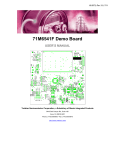
19-5650; Rev 1.0; 1/11 A Maxim Integrated Products Brand 73S8014BN Demo Board User Manual January 2011 Rev. 1.0 UM_8014BN_069 73S8014BN Demo Board User Manual UM_8014BN_069 Maxim cannot assume responsibility for use of any circuitry other than circuitry entirely embodied in a Maxim product. No circuit patent licenses are implied. Maxim reserves the right to change the circuitry and specifications without notice at any time. Maxim Integrated Products, 120 San Gabriel Drive, Sunnyvale, CA 94086 408-737-7600 2011 Maxim Integrated Products Maxim is a registered trademark of Maxim Integrated Products. UM_8014BN_069 73S8014BN Demo Board User Manual Table of Contents 1 Introduction.......................................................................................................................................... 4 1.1 General ..........................................................................................................................................4 1.2 Safety and ESD Notes ..................................................................................................................4 1.3 Recommended Operating Conditions and Absolute Maximum Ratings.......................................5 1.3.1 Recommended Operating Conditions ......................................................................................5 1.3.2 Absolute Maximum Ratings ......................................................................................................5 1.4 Getting Started ..............................................................................................................................6 2 Design Considerations ....................................................................................................................... 7 2.1 General Layout Rules ...................................................................................................................7 2.2 Optimization for Compliance with NDS .........................................................................................7 3 Demo Board Hardware Description .................................................................................................. 8 3.1 Jumpers, Switches, and Test Points .............................................................................................8 3.2 73S8014BN Pin Description........................................................................................................10 3.3 73S8014BN Pinout (Top View) ...................................................................................................12 3.4 Schematic....................................................................................................................................13 3.5 Bill of Materials ............................................................................................................................14 3.6 PCB Layouts ...............................................................................................................................15 4 Demo Board Errata............................................................................................................................ 18 5 Ordering Information ........................................................................................................................ 18 6 Contact Information .......................................................................................................................... 18 Revision History ........................................................................................................................................ 19 Rev. 1.0 3 73S8014BN Demo Board User Manual 1 1.1 UM_8014BN_069 Introduction General The Teridian Semiconductor Corporation (TSC) 73S8014BN demo board is a platform for evaluating the Teridian 73S8014BN smart card interface IC. It incorporates the 73S8014BN integrated circuit, and it has been designed to operate either as a stand-alone platform (to be used in conjunction with an external microcontroller) or as a daughter card to be used in conjunction with the 73S12xxF evaluation platform. The 73S8014BN uses the CMDVCC and 5V/3V control signals to generate VCC (smart card supply voltage) at 1.8V, 3V, or 5V. The 73S8014BN uses a single multilevel clock-divider signal, CLKDIV, to select between a divide by 1, 2, 4, and 8 for the smart card CLK output. The demo board uses a resistor divider on two pins to generate the multilevel signal for the clock divider. Refer to the 73S8014BN IC data sheet for details. The board has been designed to comply with the NDS specification. Figure 1: 73S8014BN Demo Board Note: This board does not contain the required 20k pulldown resistor on VCC for 1.8V operation. See Section 4 for details. 1.2 Safety and ESD Notes Connecting live voltages to the demo board system results in potentially hazardous voltages on the boards. Extreme caution should be taken when handling the demo boards after connection to live voltages! The demo boards are ESD sensitive! ESD precautions should be taken when handling these boards! 4 Rev. 1.0 UM_8014BN_069 1.3 73S8014BN Demo Board User Manual Recommended Operating Conditions and Absolute Maximum Ratings 1.3.1 Recommended Operating Conditions PARAMETER RATING Supply Voltage Range, VDD 2.7V to 3.6V DC Supply Voltage Range, VPC 4.75V to 5.5V DC (ISO 7816 and EMV applications) 4.85V to 5.5V DC (NDS applications) Ambient Operating Temperature Range -40°C to +85°C Input Voltage Range for Digital Inputs 0V to (VDD + 0.3V) 1.3.2 Absolute Maximum Ratings Operation outside these rating limits may cause permanent damage to the device. PARAMETER RATING Supply Voltage Range, VDD -0.5V to +4.0V DC Supply Voltage Range, VPC -0.5V to +6.0V DC Input Voltage Range for Digital Inputs -0.3V to (VDD + 0.5V) DC Storage Temperature Range -60C to +150C Pin Voltage Range -0.3 to (VDD + 0.5V) DC Pin Current 100mA ESD Tolerance—Card Interface Pins 6kV ESD Tolerance—Other Pins 2kV Note: ESD testing on card pins is Human Body Model (HBM) condition, three pulses, each polarity referenced to ground. Rev. 1.0 5 73S8014BN Demo Board User Manual 1.4 UM_8014BN_069 Getting Started Figure 2 shows the basic connections of the demo board. Power Supplies: Apply 3.3V to pin 10 of J4 and 5V to pin 10 of J2. Control signals to the device can be connected through J2 and J4 (see Figure 2 and the electrical schematic Figure 4). Setting the clock frequency with an external clock source: o Set JP1 to the SCLK setting. o Apply clock source to pin 1 of J2. o Apply 3.3V (1) or GND (0) to CLKDIV1 and CLKDIV2 pins allows the following: - CLKDIV1 = CLKDIV2 = 0 clock frequency = SCLK/4 - CLKDIV1 = 0, CLKDIV2 =1 clock frequency = SCLK - CLKDIV1 = 1, CLKDIV2 =0 clock frequency = SCLK/8 - CLKDIV1 = CLKDIV2 = 1 (or leaving both open) clock frequency = SCLK/2 Setting the clock frequency using crystal Y1: o Crystal included in the demo board is 12MHz (NDS applications can use up to 27MHz). o Set JP1 to XTAL position. o Apply 3.3V (1) or GND (0) to CLKDIV1 and CLKDIV2 pins allows the following: - CLKDIV1 = CLKDIV2 = 0 clock frequency = 3MHz - CLKDIV1 = 0, CLKDIV2 =1 clock frequency = 12MHz - CLKDIV1 = 1, CLKDIV2 = 0 clock frequency = 1.5MHz - CLKDIV1 = CLKDIV2 = 1 (or leaving both open) clock frequency = 6MHz External clock source. JP1 must be in position SCLK when use of an external clock. Otherwise, pin SCLK can be left open. 1 SCLK VDD Power Supply: +2.7V to +3.6V (3.3V Typ.) / 50mA VDD GND IOUC RSTIN CMDVCC OFF GND 5V/#V CKDIV2 2 CKDIV1 VPC VPC Power Supply: +4.5V to +5.5V (5V Typ.) /200mA Figure 2: 73S8014BN Demo Board: Basic Connections 6 Rev. 1.0 UM_8014BN_069 2 2.1 73S8014BN Demo Board User Manual Design Considerations General Layout Rules Keep the CLK signal as short as possible and with few bends in the trace. Keep route of the CLK trace to one layer (avoid vias to other plane). Keep CLK trace away from other traces, especially RST and VCC. Filtering of the CLK trace is allowed for noise purposes. Up to 30pF to ground is allowed at the CLK pin of the smart card connector. Also, the 0 series resistor, R7, can be replaced for additional filtering (no more than 100). Keep the VCC trace as short as possible. Make trace a minimum of 0.5mm thick. Also, keep VCC away from other traces especially RST and CLK. Keep RST trace away from VCC and CLK traces. Up to 30pF to ground is allowed for filtering. Keep 0.1F close to the VDD pin of the device and directly take other end to ground. Keep 0.1F and 10F close to the VPC pin of the device and directly take other end to ground. Keep 1.0F close to the VCC pin of the smart card connector and directly take other end to ground 2.2 Optimization for Compliance with NDS Default configuration of the demo board contains a 27pF capacitor (C12) from the CLK pin of the smart connector to ground and a 27pF capacitor (C13) from the RST pin of the smart connector to ground. These capacitors serve as filters for the CLK and RST signals in the case of long traces or test equipment perturbations. The capacitor on CLK reduces ringing on the trace, reduces coupling to other traces and slows down the edge of the CLK signal. The capacitor on RST helps the perturbation specification in a noisy environment. The filter capacitors can be useful in the EMV test environment and have no effect on NDS testing. C12 and C13 are represented on both the schematic and BOM. These capacitors are optional filter capacitors on the smart card lines CLK and RST, respectively, for each card interface. These capacitors can be adjusted (value, not to exceed 30pF) or removed to optimize performance in each specific application (PCB, card clock frequency, compliance with applicable standards, etc.). Rev. 1.0 7 73S8014BN Demo Board User Manual 3 UM_8014BN_069 Demo Board Hardware Description 3.1 Jumpers, Switches, and Test Points The items described in the following tables refer to the flags in Figure 3. Table 1: Demo Board Description ITEM (FIGURE 3) 8 SCHEMATIC AND PCB SILKSCREEN REFERENCE 1 J2 2 3 4 5 9 10 TP8 TP7 TP5 TP3 TP4 TP6 NAME USE Board 5V supply and host digital interface Connector that gathers the 5V supply of the board, the 73S8014BN data interface (I/OUC, C4UC, and C8UC), external clock (SCLK), and interrupt (OFF) pins. Note that the external clock (SCLK) can be left open when JP1 is in position XTAL. Test Points: C4 CLK RST VCC I/O C8 2-pin test points for each respective smart card signal. The pin label name is the respective signal (i.e., VCC, CLK) and the other pin is GND. 6 J4 Board 3.3V Supply and Digital Control Signals 7 Y2 Resonator (Optional) A footprint is available to accommodate an optional ceramic resonator in place of the crystal oscillator. Connector that gathers the 3.3V supply of the board, the 73S8014BN host control signal pins RSTIN, CMDVCC, 5V/3V, CLKDIV2, and CLKDIV1. 8 J6 Smart Card Connector SIM/SAM smart card format connector. Note that J6 is wired is parallel to the smart card connector J5 (underneath the PCB). No SIM/SAM should be inserted when using the credit card size connector J5. 11 JP1 Clock Selection Jumper to select between a crystal and external clock as the frequency reference to the device. The default setting is for a crystal. 12 J5 Smart Card Connector Smart card connector. When inserting a card (credit card size format), contacts must face up. Rev. 1.0 UM_8014BN_069 73S8014BN Demo Board User Manual 4 2 3 5 1 6 7 12 11 10 9 8 Figure 3: Teridian 73S8014BN Demo Board: Board Description Rev. 1.0 9 73S8014BN Demo Board User Manual 3.2 UM_8014BN_069 73S8014BN Pin Description Table 2: 73S8014BN Pin Description: Card Interface NAME PIN DESCRIPTION I/O 13 Card I/O: Data Signal to/from Card. Includes a pullup resistor to VCC. C4 12 Card C4: Data Signal to/from Card. Includes a pullup resistor to VCC C8 14 Card C8: Data Signal to/from Card. Includes a pullup resistor to VCC RST 15 Card Reset. Provides reset (RST) signal to card. CLK 17 Card Clock. Provides clock signal (CLK) to card. The rate of this clock is determined by crystal oscillator frequency or external clock input and CLKDIV selections. PRES 19 Card Presence Switch. Active high indicates card is present. Includes a highimpedance pulldown current source. The PRES input includes a 5ms debounce for card insertion. VCC 18 Card Power Supply. Logically controlled by sequencer, output of LDO regulator. Requires an external filter capacitor to the card GND. GND 16 Device Ground Table 3: 73S8014BN Pin Description: Miscellaneous and Outputs NAME PIN DESCRIPTION XTALIN 10 Crystal Oscillator Input. Can either be connected to the crystal or driven as a source for the card clock. XTALOUT 11 Crystal Oscillator Output. Connected to the crystal. Left open if XTALIN is being used as external clock input. Table 4: 73S8014BN Pin Description: Power Supply and Ground 10 NAME PIN DESCRIPTION VDD 7 System Interface Supply Voltage and Supply Voltage for Internal Circuitry VPC 4 LDO Regulator Power Supply Source Rev. 1.0 UM_8014BN_069 73S8014BN Demo Board User Manual Table 5: 73S8014BN Pin Description: Microcontroller Interface NAME PIN CMDVCC 8 5V/3V 9 DESCRIPTION Command VCC (Negative Assertion): Logic-low on this pin causes the LDO regulator to ramp the VCC supply to the card and initiates a card activation sequence, if a card is present. 5V/3V/1.8V Card Selection. Logic-high selects 5V for VCC and card interface. Logic-low selects 3V operation. Logic going from high to low within 400ns of CMDVCC falling selects 1.8V. When the device is used with a single card voltage (3V or 5V only), this pin should be connected to either GND or VDD. However, it includes a high-impedance pullup resistor to default this pin high (selection of 5V card) when not connected. This pin has no effect after CMDVCC is low. Sets the divide ratio from the XTAL oscillator (or external clock input) to the card clock. This is a multilevel input that uses a ratio of the VDD voltage to select the clock divider as shown below. Note: This input has no internal pullup or pulldown so it must not be allowed to be left unconnected. CLKDIV 6 CLKDIV CLOCK RATE GND XTALIN/4 VDD/3 XTALIN VDD x 2/3 XTALIN/8 VDD XTALIN/2 OFF 20 Active-Low Interrupt Signal to the Processor. Multifunction indicating fault conditions or card presence. Open-drain output configuration. This pin includes an internal 22k pullup to VDD. RSTIN 1 Reset Input. This signal is the reset command to the card. I/OUC 3 System Controller Data I/O to/from the Card. Includes a pullup resistor to VDD. C4UC 5 System Controller Data C4 to/from the Card. Includes a pullup resistor to VDD. C8UC 2 System Controller Data C8 to/from the Card. Includes a pullup resistor to VDD. Rev. 1.0 11 73S8014BN Demo Board User Manual 3.3 UM_8014BN_069 73S8014BN Pinout (Top View) Figure 4: 73S8014BN Pinout 12 Rev. 1.0 UM_8014BN_069 3.4 73S8014BN Demo Board User Manual Schematic J1 SCLK SIO SC4 SC8 OFFB GND GND GND +5V +5V 1 2 3 4 5 6 7 8 9 10 5.0V 3.3V C1 C2 1 2 3 4 5 6 7 8 9 10 (VDD) 3.3V 0.1uF U1 R5 1 2 3 4 5 6 7 8 9 10 100K 5.0V C3 R2 1K 10uF TSM_110_01_L_SV J3 CLKDIV1 CLKDIV2 5V3VB CMDVCCB RSTIN GND +3.3V 1 2 3 4 5 6 7 8 9 10 R3 OFF PRES VCC CLK GND RST C8 I/O C4 XTALOUT 20 19 18 17 16 15 14 13 12 11 R7 0 R4 73S8014BN 0 XTAL R6 SCLK Y1 2 12.000MHz 1 C4 C5 Y2 3 2 1 1M 22pF 1 2 22pF JP1 3 USR0 USR1 USR2 USR3 USR4 USR5 USR6 USR7 XTALIN SELECT When using external clock source set JP1 for SCLK and remove JP2. When using crystal, set JP1 for XTAL. 3.3V C10 TSM_110_01_L_SV + 1 2 3 4 5 6 7 8 9 10 RSTIN C8UC I/OUC VPC C4UC CLKDIV VDD CMDVCC 5V/3V XTALIN 2K SSM_110_L_SV J4 0.1uF C8 SCLK SIO S_C4 S_C8 INT2 + J2 C1, C2 and C8 must be placed within 5mm of the U1 pins and connected by thick track (wider than 0.5mm) 10uF + SSM_110_L_SV TP4 I/O Y2 is an optional footprint for a ceramic resonator TP3 1 2 1 2 TP6 C8 VCC TP5 1 2 1 2 10uF RST TP7 1 2 TP3 to TP8 should be placed very close to the pads of J5 CLK TP8 J1 and J3 are placed on the bottom. are placed on the top side. J2 and J4 1 2 R1 J1 and J3 must be aligned with J8 and J9 on the 1121 evaluation board (E1121T8), respectively, in order for this board to be stacked on it. C4 100K (VDD) J5 Smart Card Connector C12 C13 C11 27pF 27pF 1uF Capacitors C11, C12 and C13 should be placed very close to the pads of J5 SW2 SW1 C7 C6 C5 C3 C2 C1 C8 I/O VPP GND C4 CLK RST VCC SW-2 SW-1 8 7 6 5 4 3 2 1 8 7 6 5 4 3 2 1 3.3V 10 9 J1 must be aligned with J2 and J3 must be aligned with J4 in order for this daughter board to be stacked on another. J6 SIM/SAM Connector Figure 5: Teridian 73S8014BN Demo Board: Electrical Schematic Rev. 1.1 13 73S8014BN Demo Board User Manual 3.5 UM_8014BN_069 Bill of Materials Table 6: Teridian 73S8014BN Demo Board: Bill of Materials PCB FOOTPRINT DIGI-KEY PART NUMBER 10F, 6.3V X5R ceramic capacitors (0805) 805 PCC2225CT-ND ECJ-2FB0J106M Panasonic C2, C8 0.1F, 16V X7R ceramic capacitors (0603) 603 PCC1762CT-ND ECJ-1VB1C104K Panasonic 2 C4, C5 22pF, 50V SMD ceramic capacitors (0603) 603 PCC220ACVCT-ND ECJ-1VC1H220J Panasonic 1 C11 1F, 6.3V X5R ceramic capacitor (0603) 603 2 C12, C13 27pF, 50V SMD ceramic capacitors (0603) 603 2 J1, J3 10-pin SMD connectors SSM_110_L_SV N/A SSM_110_L_SV Samtec 2 J2, J4 10-pin SMD connectors TSM_110_01_L_SV N/A TSM_110_01_L_SV Samtec 1 J5 8-pin smart card SMD connector with 2-pin switch CCM02-2504 401-1715-ND CCM02-2504LFT C&K Components 1 J6 6-pin SIM/SAM smart card SMD connector with 2-pin switch ITT_CCM03-3013 401-1726-2-ND CCM03-3754 R102 C&K Components 1 JP1 3 pins, 2.54mm pitch S1011E-36-ND PZC36SAAN Sullins Connector Solutions 2 R1, R5 100k 5%, 1/10W SMD resistors (0603) 603 P100KGCT-ND ERJ-3GEYJ104V Panasonic 1 R2 1k 5%, 1/10W SMD resistor (0603) 603 P1.0KGCT-ND ERJ-3GEYJ102V Panasonic 1 R3 2k 5%, 1/10W SMD resistor (0603) 603 P2.0KGCT-ND ERJ-3GEYJ202V Panasonic 2 R4, R7 0 5%, 1/10W SMD resistors (0603) 603 P0.0GCT-ND ERJ-3GEY0R00V Panasonic 1 R6 1M 5%, 1/10W SMD resistor (0603) 603 P1.0MGCT-ND ERJ-3GEYJ105V Panasonic 6 TP3–TP8 2 pins, 2.54mm pitch S1011E-36-ND PZC36SAAN Sullins Connector Solutions 1 Y1 12.000MHz, 20pF 49US crystal HC-49US X1116-ND ECS-120-20-4XDN ECS, Inc. 0 Y2 Not installed, crystal N/A N/A N/A N/A 1 U1 Smart card interface 20 SO N/A 73S8014BN-IL/F Teridian Semiconductor QTY REFERENCE 3 C1, C3, C10 2 14 PART 3-pin header 2-pin headers (test points) PCC1915CT-ND PART NUMBER MANUFACTURER ECJ-1VB0J105K Panasonic PCC270ACVCT-ND ECJ-1VC1H270J Panasonic Rev. 1.1 UM_8014BN_069 3.6 73S8014BN Demo Board User Manual PCB Layouts Figure 6: Teridian 73S8014BN Demo Board: Top View Figure 7: Teridian 73S8014BN Demo Board: Bottom View Rev. 1.0 15 73S8014BN Demo Board User Manual UM_8014BN_069 Figure 8: Teridian 73S8014BN Demo Board: Top Signal Layer Figure 9: Teridian 73S8014BN Demo Board: Middle Layer 1, Ground Plane 16 Rev. 1.0 UM_8014BN_069 73S8014BN Demo Board User Manual Figure 10: Teridian 73S8014BN Demo Board: Middle Layer 2, Supply Plane Figure 11: Teridian 73S8014BN Demo Board: Bottom Signal Layer Rev. 1.0 17 73S8014BN Demo Board User Manual 4 UM_8014BN_069 Demo Board Errata The VCC output supply when operating at 1.8V requires a minimum 20k load resistor to ground for output voltage stability. The demo board does not contain a footprint for this resistor. If using VCC = 1.8V this resistor must be added to provide proper output voltage stability. 5 6 Ordering Information PART DESCRIPTION ORDERING NUMBER 73S8014BN Demo Board 73S8014BN-EVK Contact Information For more information about Maxim products or to check the availability of the 73S8014BN, contact technical support at www.maxim-ic.com/support. 18 Rev. 1.0 UM_8014BN_069 73S8014BN Demo Board User Manual Revision History REVISION NUMBER REVISION DATE 1.0 1/11 Rev. 1.0 DESCRIPTION Initial release PAGES CHANGED — 19