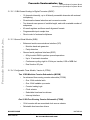
1
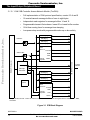
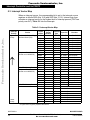
Freescale Semiconductor, Inc.
M•CORE™
Freescale Semiconductor, Inc...
M•CORE Evaluation System
User’s Manual
Revision 1.0
Motorola reserves the right to make changes without further notice to any products herein to improve reliability, function or
design. Motorola does not assume any liability arising out of the application or use of any product or circuit described herein;
neither does it convey any license under its patent rights nor the rights of others. Motorola products are not designed, intended,
or authorized for use as components in systems intended for surgical implant into the body, or other applications intended to
support or sustain life, or for any other application in which the failure of the Motorola product could create a situation where
personal injury or death may occur. Should Buyer purchase or use Motorola products for any such unintended or unauthorized
application, Buyer shall indemnify and hold Motorola and its officers, employees, subsidiaries, affiliates, and distributors
harmless against all claims, costs, damages, and expenses, and reasonable attorney fees arising out of, directly or indirectly,
any claim of personal injury or death associated with such unintended or unauthorized use, even if such claim alleges that
Motorola was negligent regarding the design or manufacture of the part. Motorola and are registered trademarks of Motorola,
Inc. Motorola, Inc. is an Equal Opportunity/Affirmative Action Employer.
The M•CORE name and logotype and the OnCE name are trademarks of Motorola, Inc.
© Motorola, Inc. 1998
For More Information On This Product,
Go to: www.freescale.com
Freescale Semiconductor, Inc.
M•CORE Evaluation System User’s Manual
Freescale Semiconductor, Inc...
M•CORE Evaluation System User’s Manual
MOTOROLA
ii
MCOREEVSUM/D
For More Information On This Product,
Go to: www.freescale.com
User’s Manual
Freescale Semiconductor, Inc.
Table of Contents
Freescale Semiconductor, Inc...
Section 1 Introducing the M•CORE Evaluation System
1.1
1.1.1
1.1.2
1.1.3
1.2
1.3
1.4
1.5
The M•CORE Evaluation System . . . . . . . . . . . . . . . . . . . . . . . . . . . . . 1
CPU Memory Board . . . . . . . . . . . . . . . . . . . . . . . . . . . . . . . . . . . . . 1
Input/Output Peripheral Board . . . . . . . . . . . . . . . . . . . . . . . . . . . . . 1
Target Interface Board . . . . . . . . . . . . . . . . . . . . . . . . . . . . . . . . . . . 2
M•CORE Evaluation System Features . . . . . . . . . . . . . . . . . . . . . . . . . 2
M•CORE Evaluation System Block Diagram . . . . . . . . . . . . . . . . . . . . 3
M•CORE Evaluation System Specifications . . . . . . . . . . . . . . . . . . . . . 3
References . . . . . . . . . . . . . . . . . . . . . . . . . . . . . . . . . . . . . . . . . . . . . . 4
Section 2 The CPU Memory Board
2.1
CMB Options. . . . . . . . . . . . . . . . . . . . . . . . . . . . . . . . . . . . . . . . . . . . . 5
2.1.1
Mode Select Jumper (J22) . . . . . . . . . . . . . . . . . . . . . . . . . . . . . . . . 5
2.1.2
MDTACK/MDS Jumper (J21-13 and J21-15) . . . . . . . . . . . . . . . . . . 6
2.1.3
TRST Select Jumper (J99) . . . . . . . . . . . . . . . . . . . . . . . . . . . . . . . . 7
2.2
CMB Connectors. . . . . . . . . . . . . . . . . . . . . . . . . . . . . . . . . . . . . . . . . . 7
2.2.1
Serial 1 (J24) and Serial 2 (J25) Connectors . . . . . . . . . . . . . . . . . . 7
2.2.2
Power Connector (TB1) . . . . . . . . . . . . . . . . . . . . . . . . . . . . . . . . . . 8
2.2.3
Data Bus Connectors (J10, J11, J13, J14). . . . . . . . . . . . . . . . . . . . 8
2.2.4
Address Bus Connectors (J4, J5, J7, J8) . . . . . . . . . . . . . . . . . . . . . 9
Section 3 The Input/Output Peripheral Board
3.1
Introducing the Input/Output Peripheral Board . . . . . . . . . . . . . . . . . . 11
3.1.1
IPB Block Diagram . . . . . . . . . . . . . . . . . . . . . . . . . . . . . . . . . . . . . 11
3.1.2
Peripheral Slave Devices . . . . . . . . . . . . . . . . . . . . . . . . . . . . . . . . 11
3.1.2.1
CAN 2.0B Controller Access Network Module (TouCAN) . . . . . 12
3.1.2.2
10-Bit Queued Analog-to-Digital Converter (QADC) . . . . . . . . . 13
3.1.2.3
Queued Serial Module (QSM) . . . . . . . . . . . . . . . . . . . . . . . . . . 13
3.1.2.4
Configurable Timer Module, Version 4 (CTM4) . . . . . . . . . . . . . 13
3.1.3
General-Purpose Inputs and Outputs. . . . . . . . . . . . . . . . . . . . . . . 15
3.1.4
Bus and Control Signals . . . . . . . . . . . . . . . . . . . . . . . . . . . . . . . . . 15
3.2
IPB Options. . . . . . . . . . . . . . . . . . . . . . . . . . . . . . . . . . . . . . . . . . . . . 15
MCOREEVSUM/D
User’s Manual
MOTOROLA
For More Information On This Product,
Go to: www.freescale.com
iii
Freescale Semiconductor, Inc.
Table of Contents
3.2.1
3.2.2
3.2.2.1
3.2.2.2
3.2.2.3
3.2.3
3.2.4
QADC Voltage Reference Source (W14, W15) . . . . . . . . . . . . . . . 15
General-Purpose Input/Output (W1 through W8) . . . . . . . . . . . . . . 17
GPIO Output Control Header Pins . . . . . . . . . . . . . . . . . . . . . . . 17
Using the SDS Debugger to Access the GPIO Ports . . . . . . . . . 18
Alternate Use for GPIOH and GPIOG Pins . . . . . . . . . . . . . . . . 18
W10 Jumper . . . . . . . . . . . . . . . . . . . . . . . . . . . . . . . . . . . . . . . . . . 18
W13 Jumper . . . . . . . . . . . . . . . . . . . . . . . . . . . . . . . . . . . . . . . . . . 18
Freescale Semiconductor, Inc...
Section 4 Memory Maps and Pinouts
4.1
IPB Memory Maps . . . . . . . . . . . . . . . . . . . . . . . . . . . . . . . . . . . . . . . 19
4.1.1
EVS Base Addresses . . . . . . . . . . . . . . . . . . . . . . . . . . . . . . . . . . . 19
4.1.2
Peripheral Slave Device Memory Map . . . . . . . . . . . . . . . . . . . . . . 19
4.1.3
Interrupt Controller Memory Map . . . . . . . . . . . . . . . . . . . . . . . . . . 20
4.1.4
GPIO Memory Map. . . . . . . . . . . . . . . . . . . . . . . . . . . . . . . . . . . . . 21
4.2
Target Interface Board Pinouts . . . . . . . . . . . . . . . . . . . . . . . . . . . . . . 21
Section 5 Interrupt Controller and its PORTF
5.1
5.1.1
5.1.2
5.1.3
5.1.4
5.1.5
5.2
5.3
5.4
5.4.1
5.4.2
5.4.3
5.4.4
5.4.5
5.4.6
Interrupt Controller Registers . . . . . . . . . . . . . . . . . . . . . . . . . . . . . . . 25
Interrupt Source Register 1 (ISR1) . . . . . . . . . . . . . . . . . . . . . . . . . 25
Interrupt Source Register 2 (ISR2) . . . . . . . . . . . . . . . . . . . . . . . . . 25
Interrupt Enable Register 1 (IER1) . . . . . . . . . . . . . . . . . . . . . . . . . 26
Interrupt Enable Register 2 (IER2) . . . . . . . . . . . . . . . . . . . . . . . . . 26
Fast Interrupt Enable Register (FIER) . . . . . . . . . . . . . . . . . . . . . . 27
Controlling Interrupts. . . . . . . . . . . . . . . . . . . . . . . . . . . . . . . . . . . . . . 27
Interrupt Vector Map . . . . . . . . . . . . . . . . . . . . . . . . . . . . . . . . . . . . . . 28
Interrupt Controller Port F . . . . . . . . . . . . . . . . . . . . . . . . . . . . . . . . . . 29
Interrupt Controller Port F Edge Control Register (PFECR). . . . . . 29
Interrupt Controller Port F Interrupt Enable Register (PFIER) . . . . 30
Interrupt Controller Port F Data Direction Register (DDRF) . . . . . . 30
Interrupt Controller Port F Output Data Register (PORTF) . . . . . . 31
Interrupt Controller Port F Pin Data Register (PORTFP) . . . . . . . . 31
Interrupt Controller Port F Edge-Detect Register (PORTFE) . . . . . 31
MOTOROLA
iv
MCOREEVSUM/D
For More Information On This Product,
Go to: www.freescale.com
User’s Manual
Freescale Semiconductor, Inc.
Freescale Semiconductor, Inc...
List of Figures
Figure 1-1
Figure 2-1
Figure 2-2
Figure 3-1
Figure 3-2
Figure 3-3
Figure 4-1
Figure 4-2
M•CORE Evaluation System Block Diagram . . . . . . . . . . . . . . . 3
CMB Layout . . . . . . . . . . . . . . . . . . . . . . . . . . . . . . . . . . . . . . . . 5
Serial Connector Pinout . . . . . . . . . . . . . . . . . . . . . . . . . . . . . . . 8
IPB Block Diagram . . . . . . . . . . . . . . . . . . . . . . . . . . . . . . . . . . 12
IPB Board Layout . . . . . . . . . . . . . . . . . . . . . . . . . . . . . . . . . . . 16
W10 Jumper Position . . . . . . . . . . . . . . . . . . . . . . . . . . . . . . . . 18
Peripheral Slave Device Memory Map. . . . . . . . . . . . . . . . . . . 20
TIB Connector Layout (Left Half) . . . . . . . . . . . . . . . . . . . . . . . 22
Figure 4-3
Figure 5-1
Figure 5-2
Figure 5-3
Figure 5-4
Figure 5-5
Figure 5-6
Figure 5-7
Figure 5-8
Figure 5-9
Figure 5-10
Figure 5-11
TIB Connector Layout (Right Half) . . . . . . . . . . . . . . . . . . . . . . 23
Interrupt Source Register 1 (ISR1). . . . . . . . . . . . . . . . . . . . . . 25
Interrupt Source Register 2 (ISR2). . . . . . . . . . . . . . . . . . . . . . 25
Interrupt Enable Register 1 (IER1). . . . . . . . . . . . . . . . . . . . . . 26
Interrupt Enable Register 2 (IER2). . . . . . . . . . . . . . . . . . . . . . 26
Fast Interrupt Enable Register (FIER) . . . . . . . . . . . . . . . . . . . 27
Port F Edge (Polarity) Control Register (PFECR) . . . . . . . . . . 29
Port F Interrupt Enable Register (PFIER) . . . . . . . . . . . . . . . . 30
Port F Data Direction Register (DDRF) . . . . . . . . . . . . . . . . . . 30
Port F Output Data Register (PORTF) . . . . . . . . . . . . . . . . . . . 31
Port F Pin Data Register (PORTFP) . . . . . . . . . . . . . . . . . . . . 31
Port F Edge-Detect Register (PORTFE) . . . . . . . . . . . . . . . . . 31
MCOREEVSUM/D
User’s Manual
MOTOROLA
For More Information On This Product,
Go to: www.freescale.com
v
Freescale Semiconductor, Inc.
Freescale Semiconductor, Inc...
List of Figures
MOTOROLA
vi
MCOREEVSUM/D
For More Information On This Product,
Go to: www.freescale.com
User’s Manual
Freescale Semiconductor, Inc.
Freescale Semiconductor, Inc...
List of Tables
Table 1-1
Table 2-1
Table 2-2
Table 2-3
Table 2-4
Table 2-5
Table 2-6
Table 3-1
M•CORE Evaluation System Specifications. . . . . . . . . . . . . . . . . 3
Mode Select (J22) Jumper Positions . . . . . . . . . . . . . . . . . . . . . . 6
MDTACK (J21-13 and J21-15) Jumper Positions . . . . . . . . . . . . 6
TRST Select (J99) Jumper Positions . . . . . . . . . . . . . . . . . . . . . . 7
CMB Serial Connections . . . . . . . . . . . . . . . . . . . . . . . . . . . . . . . 7
CMB Data Bus Connection . . . . . . . . . . . . . . . . . . . . . . . . . . . . . 9
CMB Address Bus Connection. . . . . . . . . . . . . . . . . . . . . . . . . . 10
Low Voltage Reference Source Jumper (W14) . . . . . . . . . . . . . 15
Table 3-2
Table 3-3
Table 3-4
Table 3-5
Table 4-1
Table 4-2
Table 4-3
Table 5-1
High Voltage Reference Source Jumper (W15) . . . . . . . . . . . . . 16
General-Purpose Input/Output Jumpers (W1 through W8) . . . . 17
System Data Bus Lines . . . . . . . . . . . . . . . . . . . . . . . . . . . . . . . 17
GPIO Port Relation to Jumpers . . . . . . . . . . . . . . . . . . . . . . . . . 17
Base Addresses . . . . . . . . . . . . . . . . . . . . . . . . . . . . . . . . . . . . . 19
Interrupt Controller Memory Map . . . . . . . . . . . . . . . . . . . . . . . . 21
GPIO Memory Map . . . . . . . . . . . . . . . . . . . . . . . . . . . . . . . . . . 21
Interrupt Vector Map . . . . . . . . . . . . . . . . . . . . . . . . . . . . . . . . . 28
MCOREEVSUM/D
User’s Manual
MOTOROLA
For More Information On This Product,
Go to: www.freescale.com
vii
Freescale Semiconductor, Inc.
Freescale Semiconductor, Inc...
List of Tables
MOTOROLA
viii
MCOREEVSUM/D
For More Information On This Product,
Go to: www.freescale.com
User’s Manual
Freescale Semiconductor, Inc.
Section 1 Introducing the M•CORE Evaluation System
1.1 The M•CORE Evaluation System
Freescale Semiconductor, Inc...
The M•CORE™ evaluation system allows emulation of the M•CORE, a new family
of 32-bit RISC microcontrollers that are optimized for 16-bit external systems. The
M•CORE evaluation system consists of three boards:
•
CPU memory board (CMB)
•
Input/output peripheral board (IPB)
•
Target interface board (TIB)
All three boards are connected through a ring of connectors which form the
modular active probe interconnect (MAPI).
1.1.1 CPU Memory Board
The CMB contains the following components:
•
M•CORE microcontroller
•
512 Kbytes of Flash memory
•
512 Kbytes of fast static RAM
•
RS-232 interface
•
Reset and interrupt steering logic
•
Bottom-side MAPI ring to connect to the IPB
1.1.2 Input/Output Peripheral Board
The input/output peripheral board (IPB) emulates the peripheral modules for the
M•CORE microcontroller. It contains the following components:
•
Two Motorola peripheral devices operating in slave mode
•
One field-programmable gate array (FPGA) programmed to re-map
interrupts and provide edge-detect inputs and on-board chip selects
•
Eight 74FCT652s providing 64 bits of general-purpose inputs or
general-purpose outputs
•
Two sets of programmable array logic (PALs) for bus matching and chip
select steering
•
Top-side MAPI connectors for interface with the CMB
•
Bottom-side MAPI connectors for interface with the TIB
MCOREEVSUM/D
User’s Manual
MOTOROLA
For More Information On This Product,
Go to: www.freescale.com
1
Freescale Semiconductor, Inc.
Introducing the M•CORE Evaluation System
For more information about the IPB, see Section 3 The Input/Output Peripheral
Board.
1.1.3 Target Interface Board
The target interface board (TIB) provides external access to some of the signals on
the MAPI ring, typically for connecting a logic analyzer to the M•CORE evaluation
system. This board is not required for operation of the other two boards.
1.2 M•CORE Evaluation System Features
Freescale Semiconductor, Inc...
To assist in the development of an M•CORE controller, the M•CORE evaluation
system includes the following features:
•
512 Kbytes of Flash memory
•
512 Kbytes of fast static RAM
•
Manual reset switch
•
5V for Flash memory programming on the CMB
•
Direct 5V input power on the CMB
•
5V to 3.3V converter for M•CORE
•
64 bits of general-purpose input or output
•
Eight edge-detect inputs
•
Two slave peripheral devices, each providing:
– 10-bit queued analog-to-digital converter (QADC)
• Up to 16 channels of analog input each
• Four channels, programmable as external input triggers
– Two queued serial modules (QSM)
• Two queued serial peripheral interfaces (QSPI)
• Two serial communication interfaces (SCI)
– Two controller access network interfaces (TouCAN™)
– Two configurable timer modules, version 4 (CTM4)
• Four 16-bit modulus counter submodule (MCSM)
• Two 16-bit free-running counter submodules (FASM)
• Eight double-action submodules (DASM)
• Eight pulse width modulation submodules (PWMSM)
MOTOROLA
2
MCOREEVSUM/D
For More Information On This Product,
Go to: www.freescale.com
User’s Manual
Freescale Semiconductor,
Inc.
Introducing
the M•CORE Evaluation System
M•CORE Evaluation System Block Diagram
1.3 M•CORE Evaluation System Block Diagram
Figure 1-1 illustrates the block diagram of the M•CORE evaluation system.
CMB
Freescale Semiconductor, Inc...
M•CORE
512 Kbytes
FSRAM
IPB
GPOs
GPIs
J
MAPI
P
MAPI
J
MAPI
P
MAPI
J
MAPI
P
512 Kbytes
Flash Memory
Peripheral
Slave
Device 1
Peripheral
Slave
Device 2
Interrupt
Controller
TIB
MAPI
Logic Analyzer Connections (20-pin headers)
Figure 1-1 M•CORE Evaluation System Block Diagram
1.4 M•CORE Evaluation System Specifications
Table 1-1 lists the M•CORE evaluation system specifications.
Table 1-1 M•CORE Evaluation System Specifications
Characteristic
Specification
System clock
20 MHz
External clock
20 MHz
MCU I/O ports
HCMOS compatible
Operating temperature
0°C to +40°C
Storage temperature
0°C to +40°C
Relative humidity
0% to 90% (non-condensing)
Power requirements: VDD
5V @ 2 amp
MCOREEVSUM/D
User’s Manual
MOTOROLA
For More Information On This Product,
Go to: www.freescale.com
3
Freescale Semiconductor, Inc.
Introducing the M•CORE Evaluation System
1.5 References
Freescale Semiconductor, Inc...
The following documents provide additional information relevant to developing
M•CORE controllers. All of these documents are available on CD-ROM.
•
QSM Reference Manual (QSMRM/AD)
•
QADC Reference Manual (QADCRM/AD)
•
CTM4 Configurable Timer Module section excerpted from
MC68336/376UM/AD
•
TouCAN CAN 2.0 Controller Module section excerpted from
MC68336/376UM/AD
The CD-ROM that comes with the M•CORE evaluation system also contains PDF
files of relevant portions of other Motorola manuals concerning the peripheral
devices used on the IPB.
Check our web sites at www.mcu.motsps.com/lit/3xx.html and
www.mot.com/sps/mcore for additional information.
MOTOROLA
4
MCOREEVSUM/D
For More Information On This Product,
Go to: www.freescale.com
User’s Manual
Freescale Semiconductor, Inc.
Section 2 The CPU Memory Board
2.1 CMB Options
The CMB provides several configuration options for determining the board’s
operation. Options are selected by positioning shunts (jumpers) across the
appropriate jumper pins.
Freescale Semiconductor, Inc...
Figure 2-1 illustrates the layout of the CMB, including the locations of the header
blocks discussed in this chapter.
Flash Memory
Serial 2
FSRAM
J25
J1
J99
J22
3
2
1
3
2
1
8.
LED
TB1
GND
+5v
M•CORE
Core
J21
••
••
••
••
••
••
MDS • •
MDTACK • •
J24
Serial 1
MAPI
Ring
J2
J4
J3
POWER
Reset
Switch
Figure 2-1 CMB Layout
2.1.1 Mode Select Jumper (J22)
The CMB operates in one of the modes listed in Table 2-1.
MCOREEVSUM/D
User’s Manual
MOTOROLA
For More Information On This Product,
Go to: www.freescale.com
5
Freescale Semiconductor, Inc.
The CPU Memory Board
Table 2-1 Mode Select (J22) Jumper Positions
Position
Freescale Semiconductor, Inc...
3
2
1
•••
Flash Programming Mode — In Flash memory programming
mode, standalone software is used to burn code into the
on-board Flash memory. Serial 1 must be connected to a PC.
•••
3
2
1
User Mode — In user mode, the CMB copies the code in the
Flash memory to FSRAM and runs that code. Serial 1 must be
disconnected.
•••
3
2
1
Description
EVS Debug Mode — In EVS debug mode, debugger software
downloads code to the FSRAM.
2.1.2 MDTACK/MDS Jumper (J21-13 and J21-15)
Use the MDTACK/MDS jumper to tell the CMB if it is being used with or without the
IPB board, as shown in Table 2-2.
Table 2-2 MDTACK (J21-13 and J21-15) Jumper Positions
Position
13
15
13
15
••
••
••
••
••
••
••
••
••
••
••
••
••
••
••
••
Description
CMB in standalone operation
CMB with IPB
MOTOROLA
6
MCOREEVSUM/D
For More Information On This Product,
Go to: www.freescale.com
User’s Manual
Freescale Semiconductor, Inc.
The CPU Memory Board
CMB Connectors
2.1.3 TRST Select Jumper (J99)
Use the TRST select jumper to map either the OnCE TRST signal or the RESET
signal to TRST, as shown in Table 2-3.
Table 2-3 TRST Select (J99) Jumper Positions
Position
3
2
1
•••
Map OnCE TRST signal to TRST.
Map RESET to TRST.
•••
Freescale Semiconductor, Inc...
3
2
1
Description
2.2 CMB Connectors
The CMB provides the following connectors used with the various modes of
operation. Refer to Figure 2-1 to locate the connectors.
2.2.1 Serial 1 (J24) and Serial 2 (J25) Connectors
The serial 1 (J24) and serial 2 (J25) connectors provide standard nine-pin RS-232
connections to the CMB. Both connectors have the same pinout, illustrated in
Figure 2-2. The mode of operation determines which connection to use, as listed
in Table 2-4.
Table 2-4 CMB Serial Connections
Operating Mode
Serial Connector
EVS debug
Serial 2 (J25)
Flash memory programming
Serial 1 (J24)
User
No serial connection
MCOREEVSUM/D
User’s Manual
MOTOROLA
For More Information On This Product,
Go to: www.freescale.com
7
Freescale Semiconductor, Inc.
The CPU Memory Board
CD
1
RXD
3
TXD
5
DTR
7
GND
9
••
••
••
••
••
2
DSR
4
RTS
6
CTS
8
RI
10
Open
Freescale Semiconductor, Inc...
Figure 2-2 Serial Connector Pinout
2.2.2 Power Connector (TB1)
The CMB receives power at the TB1 connector. TB1 is a two lead connector: TB1-1
(red) for +5V and TB1-2 (black) for ground.
2.2.3 Data Bus Connectors (J10, J11, J13, J14)
The CMB provides read-only access to the M•CORE data bus through the J10,
J11, J13, and J14 connectors, as shown in Table 2-5.
MOTOROLA
8
MCOREEVSUM/D
For More Information On This Product,
Go to: www.freescale.com
User’s Manual
Freescale Semiconductor, Inc.
The CPU Memory Board
CMB Connectors
Table 2-5 CMB Data Bus Connection
Connector
Freescale Semiconductor, Inc...
J14
J13
J11
J10
Pin
Data Bus Bit
15
0
13
1
11
2
9
3
7
4
5
5
3
6
1
7
15
8
13
9
11
10
9
11
7
12
5
13
3
14
1
15
15
16
13
17
11
18
9
19
7
20
5
21
3
22
1
23
15
24
13
25
11
26
9
27
7
28
5
29
3
30
1
31
2.2.4 Address Bus Connectors (J4, J5, J7, J8)
The CMB provides read-only access to the M•CORE address bus through the J4,
J5, J7, and J8 connectors, as shown in Table 2-6.
MCOREEVSUM/D
User’s Manual
MOTOROLA
For More Information On This Product,
Go to: www.freescale.com
9
Freescale Semiconductor, Inc.
The CPU Memory Board
Table 2-6 CMB Address Bus Connection
Connector
Freescale Semiconductor, Inc...
J8
J7
J5
J4
Pin
Address Bus Bit
15
0
13
1
11
2
9
3
7
4
5
5
3
6
1
7
15
8
13
9
11
10
9
11
7
12
5
13
3
14
1
15
15
16
13
17
11
18
9
19
7
20
5
21
3
22
1
23
15
24
13
25
11
26
9
27
7
28
5
29
3
30
1
31
MOTOROLA
10
MCOREEVSUM/D
For More Information On This Product,
Go to: www.freescale.com
User’s Manual
Freescale Semiconductor, Inc.
Section 3 The Input/Output Peripheral Board
3.1 Introducing the Input/Output Peripheral Board
The input/output peripheral board (IPB) emulates the peripheral modules for the
M•CORE. The IPB contains the following modules and components:
•
Two Motorola peripheral slave devices. Each device provides the following
modules:
Freescale Semiconductor, Inc...
– CAN 2.0B controller module (TouCAN)
– Queued analog-to-digital controller (QADC)
– Queued serial module (QSM)
– Configurable timer module, version 4 (CTM4)
•
One field-programmable gate array (FPGA) programmed to re-map
interrupts and provide edge-detect inputs and on-board chip selects
•
Eight 74FCT652s providing 64 bits of general-purpose input (GPI) or
general-purpose output (GPO)
•
Jumpers for selecting latched output or input for the general-purpose
input/output
•
Two sets of programmable array logic (PALs) for bus matching and chip
select steering
•
Top-side MAPI connectors for interface with the CMB
•
Bottom-side MAPI connectors for interface with the TIB
3.1.1 IPB Block Diagram
Figure 3-1 illustrates the block diagram of the IPB.
3.1.2 Peripheral Slave Devices
This section gives more details about the capabilities of each Motorola peripheral
slave device. For more detailed information about each module, see the
documents listed in 1.5 References.
MCOREEVSUM/D
User’s Manual
MOTOROLA
For More Information On This Product,
Go to: www.freescale.com
11
Freescale Semiconductor, Inc.
The Input/Output Peripheral Board
3.1.2.1 CAN 2.0B Controller Access Network Module (TouCAN)
•
Full implementation of CAN protocol specification, version 2.0 A and B
•
16 receive/transmit message buffers of zero to eight bytes
•
Independent mask registers for message buffers 14 and 15
•
Programmable transmit-first scheme: lowest ID or lowest buffer number
•
16-bit free-running timer for message time stamping
•
Low-power sleep mode with programmable wake-up on bus activity
Freescale Semiconductor, Inc...
GPIOA[0:7]
GPIOB[0:7]
Data Bus
GPIOC[0:7]
GPIOD[0:7]
Peripheral
Slave
Device 1*
TouCAN
Address Bus
QSM
CTM
QADC
EXTINT[0:7]
Interrupt
Controller
GPIOG[0:7]
GPIOH[0:7]
IPB MAPI Connector
IPB MAPI Connector
Interrupt
Requests
To Target
I/F Board
GPIOD[0:7]
GPIOE[0:7]
PALs
Peripheral
Slave
Device 2*
Interrupt
Requests
TouCAN
QSM
CTM
QADC
*Peripheral slave devices 1 and 2 are software compatible with an MC68376 with regards to the TouCAN, QADC, QSM,
and CTM4.
Figure 3-1 IPB Block Diagram
MOTOROLA
12
MCOREEVSUM/D
For More Information On This Product,
Go to: www.freescale.com
User’s Manual
Freescale Semiconductor, Inc.
The Input/Output Peripheral Board
Introducing the Input/Output Peripheral Board
Freescale Semiconductor, Inc...
3.1.2.2 10-Bit Queued Analog-to-Digital Converter (QADC)
•
16 channels internally; up to 44 directly accessible channels with external
multiplexing
•
Six automatic channel selection and conversion modes
•
Two channel scan queues of variable length, each with a variable number of
subqueues
•
40 result registers and three result alignment formats
•
Programmable input sample time
•
Direct control of external multiplexers
3.1.2.3 Queued Serial Module (QSM)
•
Enhanced serial communications interface (SCI)
– Modulus baud rate generator
– Parity detection
•
Queued serial peripheral interface (QSPI)
– 80-byte static RAM to perform queued operations
– Up to 16 automatic transfers
– Continuous cycling, eight to 16 bits per transfer, LSB or MSB first
– Dual function I/O pins
3.1.2.4 Configurable Timer Module, Version 4 (CTM4)
Two 16-Bit Modulus Counter Submodules (MCSM)
•
An enhanced free-running counter submodule (FCSM)
– One 16-bit modulus latch
– One 16-bit loadable up-counter
– Counter loading logic
– Clock selector
– Selectable time-base bus drivers
– Interrupt interface
One 16-Bit Free-Running Counter Submodule (FCSM)
•
16-bit counter with an associated clock source selector
•
Selectable time-base bus drivers
MCOREEVSUM/D
User’s Manual
MOTOROLA
For More Information On This Product,
Go to: www.freescale.com
13
Freescale Semiconductor, Inc.
The Input/Output Peripheral Board
•
Control registers
•
Status bits
•
Interrupt interface
Freescale Semiconductor, Inc...
Four Double-Action Submodules (DASM)
•
Allows two 16-bit input capture or two 16-bit output compare functions to
occur automatically without software intervention
•
Input edge detector can be programmed to trigger the capture function on
user-specified edges
•
Output flip-flop can be set by one of the output compare functions and reset
by the other one
•
Interrupt requests can optionally be generated by the input capture and the
output compare functions
•
User can select one of the two incoming time bases for the input capture and
output compare functions
•
Composed of:
– Two timing channels (A and B)
– One output flip-flop
– One input edge detector
– Control logic
– Interrupt interface
Four Pulse-Width Modulation Submodules (PWMSM)
•
Allows pulse-width modulated signals to be generated over a wide range of
frequencies, independently of other CTM4 output signals
•
Output pulse-width duty cycle can vary from 0% to 100% with 16 bits of
resolution
•
Minimum pulse width is twice the MCU system clock period
•
Composed of:
– Output flip-flop with output polarity control
– Clock prescaler and selection logic
– 16-bit up-counter
– Two registers to hold the current and next pulse-width values
– Two registers to hold the current and next pulse-period values
– Pulse-width comparator
MOTOROLA
14
MCOREEVSUM/D
For More Information On This Product,
Go to: www.freescale.com
User’s Manual
Freescale Semiconductor, Inc.
The Input/Output Peripheral Board
IPB Options
3.1.3 General-Purpose Inputs and Outputs
The IPB uses 74FCT652s to generate the GPIOs. The 74FCT652s are 8-bit
registered bus transceivers configured to be registered on writes with loop-back on
reads. Each 74FCT652 has a corresponding jumper location which, if the jumper
is installed, configures that set of GPIOs as an input port with loop-back read. If the
jumper is not installed, the group is strictly output.
Freescale Semiconductor, Inc...
3.1.4 Bus and Control Signals
All bus and control signals are buffered before being fed to the peripheral slave
devices. The PAL controls the steering of chip select on the IPB while another PAL
handles the arbitration for access to the peripheral slave devices. The PAL
generates the control logic required for the handshaking between the CPU and the
peripheral slave devices.
3.2 IPB Options
The IPB provides several configuration options for determining the board’s
operation. Options are selected by positioning shunts (jumpers) across the
appropriate jumper pins.
Figure 3-2 illustrates the layout of the IPB, including the locations of the header
blocks discussed in this chapter.
3.2.1 QADC Voltage Reference Source (W14, W15)
The W14 and W15 headers select the source of the low-level and high-level analog
voltage references, as shown in Table 3-1 and Table 3-2.
Table 3-1 Low Voltage Reference Source Jumper (W14)
W14
3 2 1
Description
On-board low voltage reference
•••
3 2 1
External low-voltage reference through MAPI P2-12
•••
MCOREEVSUM/D
User’s Manual
MOTOROLA
For More Information On This Product,
Go to: www.freescale.com
15
Freescale Semiconductor, Inc.
The Input/Output Peripheral Board
Table 3-2 High Voltage Reference Source Jumper (W15)
W14
Description
External high-voltage reference through MAPI P3-6
3 2 1
•••
On-board high-voltage reference
3 2 1
Freescale Semiconductor, Inc...
•••
W1
W2
W3
W4
W5
W6
W7
W8
W10
321
Interrupt
Controller
J4
J1
J3
U26
W13
U27
J2
W14
W15
Figure 3-2 IPB Board Layout
MOTOROLA
16
MCOREEVSUM/D
For More Information On This Product,
Go to: www.freescale.com
User’s Manual
Freescale Semiconductor, Inc.
The Input/Output Peripheral Board
IPB Options
3.2.2 General-Purpose Input/Output (W1 through W8)
The W1 through W8 header blocks specify whether each set of GPIO signals
operate as outputs or inputs, as shown in Table 3-3.
Table 3-3 General-Purpose Input/Output Jumpers (W1 through W8)
W1–W8
2 1
••
2 1
Freescale Semiconductor, Inc...
••
Description
Jumper off specifies GPIO signals as latched output only. This is
the default position for W2, W4, W6, and W8.
Jumper on specifies GPIO signals as input only. This is the
default position for W1, W3, W5, and W7.
GPIO ports GPIOB, GPIOA, GPIOD, GPIOC, GPIOK, GPIOE, GPIOH, and
GPIOG are each eight bits wide, and must be addressed in pairs. Their pairings
and relationships to the 32-bit system data bus are as shown in Table 3-4.
Table 3-4 System Data Bus Lines
System Data Lines:
D[15:8]
D[7:0]
Corresponding GPIO Lines:
GPIO[7:1]
GPIO[7:1]
0x1200800
GPIOB
GPIOA
0x1200810
GPIOD
GPIOC
0x1200820
GPIOK
GPIOE
0x1200830
GPIOH
GPIOG
Address of Port Pair
The GPIO ports can be accessed only at the above addresses using only 16-bit
accesses. For example, separately accessing a byte at address 0x1200801 is not
allowed.
3.2.2.1 GPIO Output Control Header Pins
Each 8-bit GPIO port can be jumper-configured on the I/O peripheral board (IPB).
The GPIO ports relate to the IPB jumpers as shown in Table 3-5.
Table 3-5 GPIO Port Relation to Jumpers
Port
Jumper
GPIOB
W6
GPIOA
W2
GPIOD
W5
GPIOC
W3
GPIOK
W8
GPIOE
W4
GPIOH
W7
GPIOG
W1
MCOREEVSUM/D
User’s Manual
MOTOROLA
For More Information On This Product,
Go to: www.freescale.com
17
Freescale Semiconductor, Inc.
The Input/Output Peripheral Board
Not installing a jumper configures a port to be a latched output. Writing to a port will
cause the data pattern to be driven onto the pins of the port. Reading the port will
cause the last value written to the port to be read.
Installing a jumper causes a port to be an input. The last logic pattern written to a
port is not driven onto the pins of the port. Reading the port reads the logic pattern
at the pins of the port as driven by an external device.
3.2.2.2 Using the SDS Debugger to Access the GPIO Ports
Freescale Semiconductor, Inc...
To write a value to the GPIO ports, type the following in the command window of
the SDS debugger:
write -w address_of_port_pair_in_hex = 16-bit_value_to_write_in_hex
To read a value from the GPIO ports, type the following in the command window of
the SDS debugger:
read -rw address_of_port_pair_in_hex=short
Note that there are no spaces around the equals sign for a read.
3.2.2.3 Alternate Use for GPIOH and GPIOG Pins
The GPIOH and GPIOG pins on J7 of the target interface board (TIB) can also
have an alternate function. By relocating 16 0-ohm resistors on the IPB, the GPIOH
and GPIOG pins can instead represent the 16-bit modular active probe
interconnect (MAPI) data bus from the IPB. The data bus is not indicated on the
TIB signal name overlay (if supplied), but is indicated on the silkscreen of the TIB
itself.
3.2.3 W10 Jumper
The W10 header must have a jumper on pins 1 and 2, as shown in Figure 3-3.
3 2 1
•••
Figure 3-3 W10 Jumper Position
3.2.4 W13 Jumper
The W13 header is reserved for factory use.
MOTOROLA
18
MCOREEVSUM/D
For More Information On This Product,
Go to: www.freescale.com
User’s Manual
Freescale Semiconductor, Inc.
Section 4 Memory Maps and Pinouts
4.1 IPB Memory Maps
To use the IPB successfully, you need to know where information is stored in the
various memory components. This section contains the relevant memory maps.
Freescale Semiconductor, Inc...
4.1.1 EVS Base Addresses
The M•CORE evaluation system uses the base addresses listed in Table 4-1.
Table 4-1 Base Addresses
Base Address
Device
0x00000000
Flash memory1
0x00200000
FSRAM1
0x00400000
UART2 (Serial 2), J25 (for debugger monitor)
0x00600000
UART1 (Serial 1), J24 (for Flash programming)
0x00800000
Swap1 (write only)
0x01200000
Interrupt Controller2
0x01200800
GPIOs2
0x01203000
Peripheral slave device 12 (similar to MC68376)
0x01205000
Peripheral slave device 22 (similar to MC68376)
NOTES:
1. Bit 0 of the Swap register allows the Flash memory and FSRAM base ad-
dresses to be swapped. Setting bit 0 swaps the addresses; clearing bit 0
leaves the addresses as shown. After RESET, the monitor sets this bit.
2. These devices are 16-bit access only.
4.1.2 Peripheral Slave Device Memory Map
Figure 4-1 illustrates the memory map for either peripheral slave device 1 or 2.
Each peripheral slave device is software compatible with an MC68376 with regards
to the TouCAN, the QADC, the QSM, and the CTM4.
MCOREEVSUM/D
User’s Manual
MOTOROLA
For More Information On This Product,
Go to: www.freescale.com
19
Freescale Semiconductor, Inc.
Memory Maps and Pinouts
0xX000
0xX080
0xX200
0xX400
Freescale Semiconductor, Inc...
0xX500
0xXC00
0xXE00
Unused
TouCAN™
384 Bytes
QADC
512 Bytes
CTM4
256 Bytes
Unused
QSM
512 Bytes
Unused
0xXFFF
Note:
X = 3 for Peripheral Slave Device 1
X = 5 for Peripheral Slave Device 2
Figure 4-1 Peripheral Slave Device Memory Map
4.1.3 Interrupt Controller Memory Map
Table 4-2 lists the offset addresses for the interrupt controller registers. For
detailed information about these registers, see Section 5 Interrupt Controller
and its PORTF. Refer to Table 4-1 for a list of the base addresses. These registers
are 16-bit access only.
MOTOROLA
20
MCOREEVSUM/D
For More Information On This Product,
Go to: www.freescale.com
User’s Manual
Freescale Semiconductor, Inc.
Memory Maps and Pinouts
Target Interface Board Pinouts
Freescale Semiconductor, Inc...
Table 4-2 Interrupt Controller Memory Map
Address
Read/Write
Register
0x01200000
Read Only
Interrupt Source 1 (ISR1)
0x01200002
Read Only
Interrupt Source 2 (ISR2)
0x01200004
R/W
Interrupt Enable 1 (IER1)
0x01200006
R/W
Interrupt Enable 2 (IER2)
0x01200008
—
0x0120000A
R/W
Fast Interrupt Enable (FIER)
Port F Edge Control (PFECR)
Reserved
0x01200100
R/W
0x01200102–
0x01200108
—
0x0120010A
R/W
Port F Interrupt Enable (PFIER)
0x0120010C
R/W
Port F Data Direction (DDRF)
0x0120010E
R/W
Port F Output Data (PORTF)
0x01200110
R/W
Port F Pin Data (PORTFP)
0x01200112
R/W
Port F Edge Detect (PORTFE)
0x01200114–
0x012007FF
—
Reserved
Reserved
4.1.4 GPIO Memory Map
Table 4-3 lists the offset addresses for the GPIO registers. For a more detailed
description, refer to 3.2.2 General-Purpose Input/Output (W1 through W8).
Table 4-3 GPIO Memory Map
Address (in Hexadecimal)
Read/Write
0x01200800–0x01200801
R/W
0x01200802–0x0120080F
—
0x01200810–0x01200811
R/W
Register
GPIOA and GPIOB
Reserved
GPIOC and GPIOD
0x01200812–0x0120081F
—
0x01200820–0x01200821
R/W
Reserved
0x01200822–0x0120082F
—
0x01200830–0x01200831
R/W
0x01200832–0x0120083F
—
Reserved
0x01200840–0x01201FFF
—
Reserved
GPIOE and GPIOK
Reserved
GPIOG and GPIOH
4.2 Target Interface Board Pinouts
Figure 4-2 and Figure 4-3 show the connector layout with signal names for the left
and right halves of the target interface board (TIBA0002), respectively.
MCOREEVSUM/D
User’s Manual
MOTOROLA
For More Information On This Product,
Go to: www.freescale.com
21
Freescale Semiconductor, Inc.
Memory Maps and Pinouts
VDD
NC
GPIOE5
GPIOD7
GPIOD5
NC
NC
GPIOE7
Freescale Semiconductor, Inc...
GPIOC2
GPIOC0
•
•
•
•
•
•
•
•
•
•
•
•
•
•
•
•
•
•
•
•
NC
VRL
NC
1PQA7
EXTINT0
1PQA6
GPIOD6
1PQA5
Reserved
1PQA4
NC
1PQA3
Reserved
1PQA2
GPIOE6
1PQA1
GPIOC1
1PQA0
GND
1PQB7
J5
NC
NC
1PCS0
1TXD
2CAN_TXD
2MISO
GND
GND
NC
NC
•
•
•
•
•
•
•
•
•
•
•
•
•
•
•
•
•
•
•
•
•
•
•
•
•
•
•
•
•
•
•
•
•
•
•
•
•
•
•
•
VSSA
VDD
VSSA
NC
VSSA
GPIOH6
VSSA
GPIOH4
VSSA
GPIOH2
VSSA
GPIOH0
VSSA
GPIOG6
VSSA
GPIOG4
VSSA
GPIOG2
VSSA
GPIOG0
J6
NC
NC
1MOSI
NC
1PCS3
NC
2CAN_RXD
VSSA
GPIOC6
VSSA
GPIOC4
VSSA
GPIOC3
VSSA
NC
VSSA
NC
VSSA
GND
VSSA
J12
•
•
•
•
•
•
•
•
•
•
•
•
•
•
•
•
•
•
•
•
NC
GPIOC5
GPIOC7
1CAN_TXD
GND
1PCS2
1SCLK
GND
NC
•
•
•
•
•
•
•
•
•
•
•
•
•
•
•
•
•
•
•
•
•
•
•
•
•
•
•
•
•
•
NC
GPIOH7
GPIOH5
GPIOH3
GPIOH1
GPIOG7
GPIOG5
GPIOG3
GPIOG1
GND
J7
VSSA
NC
1PQB6
Reserved
1PQB5
NC
1PQB4
NC
1PQB3
GPIOE4
1PQB2
NC
1PQB1
GPIOE2
1PQB0
GPIOE1
VSSA
GPIOE0
VSSA
2CPWM7
J13
NC
•
•
•
•
•
•
•
•
•
•
•
•
•
•
•
•
•
•
•
•
•
•
•
•
•
•
•
•
•
•
GND
GND
GND
GND
GND
GND
GND
GND
GND
GND
J14
NC
2PCS0
GND
2PCS1
GND
2PCS2
GND
2PCS3
1CAN_RXD
NC
1RXD
NC
1PCS1
1CTM4C
1MISO
NC
NC
NC
GND
NC
J18
•
•
•
•
•
•
•
•
•
•
•
•
•
•
•
•
•
•
•
•
NC
NC
NC
NC
NC
2CTD10
2CTD9
1CTD10
1CTD9
GND
J19
Figure 4-2 TIB Connector Layout (Left Half)
MOTOROLA
22
MCOREEVSUM/D
For More Information On This Product,
Go to: www.freescale.com
User’s Manual
Freescale Semiconductor, Inc.
Memory Maps and Pinouts
Target Interface Board Pinouts
VDD
NC
GPIOB6
GPIOB4
GPIOB2
GPIOB0
GPIOA6
GPIOA4
Freescale Semiconductor, Inc...
GPIOA2
GPIOA0
•
•
•
•
•
•
•
•
•
•
•
•
•
•
•
•
•
•
•
•
NC
2PQB0
GPIOB7
2PQB1
GPIOB5
2PQB2
GPIOB3
2PQB3
GPIOB1
2PQB4
GPIOA7
2PQB5
GPIOA5
2PQB6
GPIOA3
2PQB7
GPIOA1
2PQA7
GND
VRH
J8
VDD
NC
NC
EXTINT7
GPIOD4
2CPWM5
SIZ1
GPIOE3
GPIOD3
GPIOD0
•
•
•
•
•
•
•
•
•
•
•
•
•
•
•
•
•
•
•
•
2CPWM8
2CPWM6
2CTD4
1CTD4
1CTD3
1CPWM8
1CPWM7
1CPWM6
1CPWM5
•
•
•
•
•
•
•
•
•
•
•
•
•
•
•
•
•
•
•
•
J20
•
•
•
•
•
•
•
•
•
•
VSSA
GPIOE1
VSSA
GND
VSSA
GND
VSSA
RESET
VSSA
VDD
VSSA
•
•
•
•
•
•
•
•
•
•
EXTINT7
GPIOD3
GPIOD4
GPIOD1
GPIOD0
J10
VSSA
VSSA
VSSA
VSSA
J9
NC
NC
NC
VSSA4
NC
2PQA0
NC
2PQA1
CLKOUT
2PQA2
2CTD3
2PQA3
GPIOE0
2PQA4
RESET
2PQA5
GPIOD1
2PQA6
GND
VSSA
J15
Reserved
•
•
•
•
•
•
•
•
•
•
•
•
•
•
•
•
•
•
•
•
•
•
•
•
•
•
•
•
•
•
NC
NC
NC
NC
VSSA
NC
VSSA
GPIOK7
VSSA
GPIOK5
VSSA
GPIOK4
VSSA
GPIOK2
VSSA
NC
NC
NC
VSSA
NC
J16
NC
NC
DS
NC
AS
NC
TSIZ0
EXTINT1
NC
EXTINT3
R/W
EXTINT5
NC
NC
TA
INT
NC
NC
GND
NC
•
•
•
•
•
•
•
•
•
•
•
•
•
•
•
•
•
•
•
•
•
•
•
•
•
•
•
•
•
•
•
•
•
•
•
•
•
•
•
•
NC
NC
NC
GPIOK6
NC
GPIOK3
GPIOK1
NC
GPIOD2
GND
J17
NC
NC
NC
NC
NC
NC
EXTINT2
2CTM4C
EXTINT4
2TXD
EXTINT6
NC
AVEC
NC
FINT
GND
NC
2SCLK
GND
NC
J21
•
•
•
•
•
•
•
•
•
•
•
•
•
•
•
•
•
•
•
•
NC
NC
NC
2RXD
NC
NC
GND
2MOSI
NC
GND
J22
Figure 4-3 TIB Connector Layout (Right Half)
MCOREEVSUM/D
User’s Manual
MOTOROLA
For More Information On This Product,
Go to: www.freescale.com
23
Freescale Semiconductor, Inc.
Freescale Semiconductor, Inc...
Memory Maps and Pinouts
MOTOROLA
24
MCOREEVSUM/D
For More Information On This Product,
Go to: www.freescale.com
User’s Manual
Freescale Semiconductor, Inc.
Section 5 Interrupt Controller and its PORTF
This PORTF is not associated with the peripheral slave devices’ port Fs.
5.1 Interrupt Controller Registers
Freescale Semiconductor, Inc...
The interrupt controller on the M•CORE evaluation system provides the following
registers for controlling and processing interrupt requests.
5.1.1 Interrupt Source Register 1 (ISR1)
This register and the interrupt source register 2 (ISR2) return the values of the
interrupt source signals. These registers are read only. Interrupts must be cleared
at their sources.
Address: 0x01200000
15
14
13
12
11
10
9
8
S2_IRQ7 S2_IRQ6 S2_IRQ5 S2_IRQ4 S2_IRQ3 S2_IRQ2 S2_IRQ1 UARTINT2
RESET:
X
X
X
X
X
X
X
X
7
6
5
0
0
0
4
3
Reserved
0
0
2
1
0
0
0
0
Figure 5-1 Interrupt Source Register 1 (ISR1)
Bits 15:8 — Interrupt Source Bits
These bits and the bits in interrupt source register 2 identify the source of the
interrupt.
1 = No interrupt pending.
0 = Interrupt pending.
Bits 7:0 — Reserved
Writes to these reserved bits have no effect and reads return zeros.
5.1.2 Interrupt Source Register 2 (ISR2)
This register and the interrupt source register 1 (ISR1) return the values of the
interrupt source signals. These registers are read only. Interrupts must be cleared
at their sources.
Address: 0x01200002
15
14
13
12
11
10
9
8
7
6
5
4
3
2
1
0
EXTINT7 EXTINT6 EXTINT5 EXTINT4 EXTINT3 EXTINT2 EXTINT1 EXTINT0 S1_IRQ7 S1_IRQ6 S1_IRQ5 S1_IRQ4 S1_IRQ3 S1_IRQ2 S1_IRQ1 UARTINT1
RESET:
X
X
X
X
X
X
X
X
X
X
X
X
X
X
X
X
Figure 5-2 Interrupt Source Register 2 (ISR2)
MCOREEVSUM/D
User’s Manual
MOTOROLA
For More Information On This Product,
Go to: www.freescale.com
25
Freescale Semiconductor, Inc.
Interrupt Controller and its PORTF
Bits 15:0 — Interrupt Source Bits
The bits in this register and in the lower byte of interrupt source register 1 identify
the source of the interrupt.
5.1.3 Interrupt Enable Register 1 (IER1)
Address: 0x01200004
RESET:
15
S2_IRQ7
0
14
S2_IRQ6
0
13
S2_IRQ5
0
12
S2_IRQ4
0
11
S2_IRQ3
0
10
S2_IRQ2
0
9
8
S2_IRQ1 UARTINT2
0
0
7
6
5
0
0
0
4
3
Reserved
0
0
2
1
0
0
0
0
Freescale Semiconductor, Inc...
Figure 5-3 Interrupt Enable Register 1 (IER1)
Bits 15:8 — Interrupt Enable Bits
The interrupt controller generates a distinct vector number to be presented to
the M•CORE VEC[n] pins. Each enabled and non-masked interrupt source
causes the CPU to fetch an interrupt vector address from the exception vector
table. Refer to Table 5-1.
1 = Interrupt is not masked.
0 = Interrupt is masked and is not presented to the VEC[n] pins.
Bits 7:0 — Reserved
Writes to these reserved bits have no effect and reads return zeros.
5.1.4 Interrupt Enable Register 2 (IER2)
Address: 0x01200006
RESET:
15
14
13
12
11
10
9
8
7
6
5
4
3
2
1
0
EXTINT7 EXTINT6 EXTINT5 EXTINT4 EXTINT3 EXTINT2 EXTINT1 EXTINT0 S1_IRQ7 S1_IRQ6 S1_IRQ5 S1_IRQ4 S1_IRQ3 S1_IRQ2 S1_IRQ1 UARTINT1
0
0
0
0
0
0
0
0
0
0
0
0
0
0
0
0
Figure 5-4 Interrupt Enable Register 2 (IER2)
Bits 15:0 — Interrupt Enable Bits
The interrupt controller generates a distinct vector number to be presented to
the M•CORE VEC[n] pins. Each enabled and non-masked interrupt source
causes the CPU to fetch an interrupt vector address from the exception vector
table. Refer to Table 5-1.
1 = Interrupt is not masked.
0 = Interrupt is masked and is not presented to the VEC[n] pins.
MOTOROLA
26
MCOREEVSUM/D
For More Information On This Product,
Go to: www.freescale.com
User’s Manual
Freescale Semiconductor, Inc.
Interrupt Controller and its PORTF
Controlling Interrupts
5.1.5 Fast Interrupt Enable Register (FIER)
Address: 0x0120000A
RESET:
15
14
13
12
11
10
9
8
EXTINT7 EXTINT6 EXTINT5 EXTINT4 EXTINT3 EXTINT2 EXTINT1 EXTINT0
0
0
0
0
0
0
0
0
7
6
5
0
0
0
4
3
Reserved
0
0
2
1
0
0
0
0
Figure 5-5 Fast Interrupt Enable Register (FIER)
Freescale Semiconductor, Inc...
The M•CORE evaluation system uses fast interrupt (FINT) priority only for the
external interrupts. The remaining interrupts cannot have a FINT priority.
EXTINT[7:0] — Fast Interrupt Enable
1 = Interrupt request pending configured as a fast interrupt source.
0 = Interrupt request pending configured as a normal interrupt source.
5.2 Controlling Interrupts
To set up the M•CORE evaluation system peripheral slave devices (similar to
MC68376s) for interrupt control, use the following procedure:
NOTE: In the register addresses for the following, X = 3 for peripheral slave device 1 and
X = 5 for peripheral slave device 2. This procedure must be completed before
enabling the peripheral slave device interrupts through the interrupt enable
registers (IER1 and IER2) in the interrupt controller.
1. Enable test mode by writing 0x0001 to the 16-bit CREG register (address
0x0120xA38).
2. Enable show IRQ by writing 0x0320 to the 16- bit SIMTR register (address
0x0120xA02). Enabling show IRQ forces information on the internal interrupt
request lines to be driven out the external IRQ pins.
3. Assign the peripheral slave device’s port F (not the interrupt controller’s port
F) to I/O by writing 0x0000 to the PFPAR register (address 0x0120xA1E).
4. Configure the peripheral slave device’s port F (not the interrupt controller’s
port F) pins for output by writing 0x00FF to the DDRF register (address
0x0120xA1C).
5. Enable interrupts from the desired onboard peripheral device module.
6. Set the interrupt level for that module to the appropriate IRQ line.
7. In the interrupt controller, enable the interrupt bit for that IRQ line.
8. Write the address for the interrupt service routine to the interrupt vector table.
MCOREEVSUM/D
User’s Manual
MOTOROLA
For More Information On This Product,
Go to: www.freescale.com
27
Freescale Semiconductor, Inc.
Interrupt Controller and its PORTF
5.3 Interrupt Vector Map
When an interrupt occurs, the corresponding bit is set in the interrupt source
registers at offsets 0000 (bits 15:0) and 0002 (bits 31:16). Internal logic then
encodes an interrupt vector for the highest level of interrupt present (FINT has
priority over INT). Table 5-1 lists the interrupts.
Table 5-1 Interrupt Vector Map
Freescale Semiconductor, Inc...
Interrupt
Priority
Highest
Priority
↑
Lowest
Priority
Device
Vector
Offset
Available for User on Target 0x0FC
Interface Board (TIB)
0x0F8
0x0F4
0x0F0
0x0EC
0x0E8
0x0E4
0x0E0
Peripheral Slave Device 1
0x0DC
(Similar to an MC68376)
0x0D8
0x0D4
0x0D0
0x0CC
0x0C8
0x0C4
J24, CPU Memory Board
0x0C0
Peripheral Slave Device 2
0x0BC
(Similar to an MC68376)
0x0B8
0x0B4
0x0B0
0x0AC
0x0A8
0x0A4
J25, CPU Memory Board
0x0A0
0x09C
0x098
0x094
0x090
0x08C
0x088
0x084
0x080
VEC[6:0]
Vector
Number
63
62
61
60
59
58
57
56
55
54
53
52
51
50
49
48
47
46
45
44
43
42
41
40
39
38
37
36
35
34
33
32
Interrupt
Type
FINT/INT
FINT/INT
FINT/INT
FINT/INT
FINT/INT
FINT/INT
FINT/INT
FINT/INT
INT
INT
INT
INT
INT
INT
INT
INT
INT
INT
INT
INT
INT
INT
INT
INT
INT
INT
INT
INT
INT
INT
INT
INT
Input Pin
Function
EXTINT7 Port F bit 7/IRQ7
EXTINT6 Port F bit 6/IRQ6
EXTINT5 Port F bit 5/IRQ5
EXTINT4 Port F bit 4/IRQ4
EXTINT3 Port F bit 3/IRQ3
EXTINT2 Port F bit 2/IRQ2
EXTINT1 Port F bit 1/IRQ1
EXTINT0 Port F bit 0/IRQ0
S1_IRQ7 User defined*
S1_IRQ6 User defined*
S1_IRQ5 User defined*
S1_IRQ4 User defined*
S1_IRQ3 User defined*
S1_IRQ2 User defined*
S1_IRQ1 User defined*
UARTINT1 UART1 interrupt
S2_IRQ7 User defined*
S2_IRQ6 User defined*
S2_IRQ5 User defined*
S2_IRQ4 User defined*
S2_IRQ3 User defined*
S2_IRQ2 User defined*
S2_IRQ1 User defined*
UARTINT2 UART2 interrupt
Reserved
Reserved
Reserved
Reserved
Reserved
Reserved
Reserved
Reserved
* Programmed through the peripheral slave device
MOTOROLA
28
MCOREEVSUM/D
For More Information On This Product,
Go to: www.freescale.com
User’s Manual
Freescale Semiconductor, Inc.
Interrupt Controller and its PORTF
Interrupt Controller Port F
5.4 Interrupt Controller Port F
Freescale Semiconductor, Inc...
The interrupt controller has a port F which is not the same as the port F in each of
the two peripheral slave devices. The interrupt controller’s port F has eight +5V
digital I/O pins. Each pin can be separately configured with software to be an input
or an output. As an input, each pin can serve as a hardware interrupt request to the
M•CORE evaluation system. The interrupt controller's port F pins are located on
the target interface board (TIB) and are labeled EXTINT7 through EXTINT0.
These pins are configured as falling edge-detect during reset. They may be
programmed as rising edge-detect. All I/O pins are configured as inputs at reset
and can be programmed as either input or output pins through the data direction
register (DDRF).
The data (output) register (PORTF) and pin state register (PORTFP) monitor and
control the states of I/O pins. Writes to PORTF cause the data to be stored in the
register and to be driven to the corresponding pins when they are programmed as
outputs. A read of PORTF returns the current value of PORTF, regardless of the
actual states of the pins. A read of PORTFP returns the current states of the
corresponding pins, regardless of whether they are inputs or outputs. Writes to
PORTFP have no effect.
Two additional registers define edge sensitivity and provide edge detection status.
The port F edge control register (PFECR) controls the edge-detection for the I/O
pins. The port F edge-detect register (PORTFE) indicates that a transition has
occurred on an I/O pin.
The port F interrupt enable register (PFIER) controls whether or not an
edge-detection on an I/O pin causes an interrupt.
5.4.1 Interrupt Controller Port F Edge Control Register (PFECR)
This register controls the edge-detect function for the port F pins.
Address: 0x01200100
RESET:
15
14
13
0
0
0
12
11
Reserved
0
0
10
9
8
0
0
0
7
PF7
0
6
PF6
0
5
PF5
0
4
PF4
0
3
PF3
0
2
PF2
0
1
PF1
0
0
PF0
0
Figure 5-6 Port F Edge (Polarity) Control Register (PFECR)
PF[x] — PORTF Pin Edge Detect
This bit controls the function of the corresponding pin.
1 = Digital I/O with rising edge detect
0 = Digital I/O with falling edge detect
MCOREEVSUM/D
User’s Manual
MOTOROLA
For More Information On This Product,
Go to: www.freescale.com
29
Freescale Semiconductor, Inc.
Interrupt Controller and its PORTF
5.4.2 Interrupt Controller Port F Interrupt Enable Register (PFIER)
The bits in this register individually enable interrupt requests generated by the
corresponding bit in the edge-detect register. If a PFIER bit is one and the
corresponding bit in the PORTFE register is set (or later becomes set when the
specified edge occurs on the corresponding pin), the interrupt controller generates
an interrupt request at the interrupt priority level specified by the interrupt vector
map. If the PFIER bit is written to zero, the interrupt controller negates the interrupt
request. Note that bits in IER2 must also be enabled.
Freescale Semiconductor, Inc...
Address: 0x0120010A
RESET:
15
14
13
0
0
0
12
11
Reserved
0
0
10
9
8
0
0
0
7
PFIER7
0
6
PFIER6
0
5
PFIER5
0
4
PFIER4
0
3
PFIER3
0
2
PFIER2
0
1
PFIER1
0
0
PFIER0
0
1
DDRF1
0
0
DDRF0
0
Figure 5-7 Port F Interrupt Enable Register (PFIER)
PFIER[7:0] — PORT F Interrupt Enable
This bit controls the function of the corresponding pin.
1 = Interrupt enabled
0 = Interrupt disabled
5.4.3 Interrupt Controller Port F Data Direction Register (DDRF)
The bits in this register control the direction of the port F pin drivers.
Address: 0x0120010C
RESET:
15
14
13
0
0
0
12
11
Reserved
0
0
10
9
8
0
0
0
7
DDRF7
0
6
DDRF6
0
5
DDRF5
0
4
DDRF4
0
3
DDRF3
0
2
DDRF2
0
Figure 5-8 Port F Data Direction Register (DDRF)
DDRF[7:0] — PORT F Data Direction (Read/Write)
Setting any bit in this register to one configures the corresponding pin as an
output. Clearing any bit in this register to zero configures the corresponding pin
as an input.
1 = Output
0 = Input
Note that interrupt requests can be generated by programming the PORTF output
data register when the DDRF selects output.
MOTOROLA
30
MCOREEVSUM/D
For More Information On This Product,
Go to: www.freescale.com
User’s Manual
Freescale Semiconductor, Inc.
Interrupt Controller and its PORTF
Interrupt Controller Port F
5.4.4 Interrupt Controller Port F Output Data Register (PORTF)
Address: 0x0120010E
RESET:
15
14
13
0
0
0
12
11
Reserved
0
0
10
9
8
0
0
0
7
6
5
4
3
2
1
0
PORTF7 PORTF6 PORTF5 PORTF4 PORTF3 PORTF2 PORTF1 PORTF0
0
0
0
0
0
0
0
0
Freescale Semiconductor, Inc...
Figure 5-9 Port F Output Data Register (PORTF)
PORTF[7:0] — PORT F Output Data (Read/Write)
The PORTF register stores the data to be driven on the port F output pins.
Reading this register returns the current value of the PORTF register, not the
states of the port F pins.
5.4.5 Interrupt Controller Port F Pin Data Register (PORTFP)
Address: 0x01200110
RESET:
15
14
13
0
0
0
12
11
Reserved
0
0
10
9
8
0
0
0
7
6
5
4
3
2
1
0
PORTFP7 PORTFP6 PORTFP5 PORTFP4 PORTFP3 PORTFP2 PORTFP1 PORTFP0
0
0
0
0
0
0
0
0
Figure 5-10 Port F Pin Data Register (PORTFP)
PORTFP[7:0] — PORT F Pin Data (Read Only)
When read, PORTFP reflects the current state of the port F pins. Writes to
PORTFP have no effect.
5.4.6 Interrupt Controller Port F Edge-Detect Register (PORTFE)
Address: 0x01200112
RESET:
15
14
13
0
0
0
12
11
Reserved
0
0
10
9
8
0
0
0
7
6
5
4
3
2
1
0
PORTFE7 PORTFE6 PORTFE5 PORTFE4 PORTFE3 PORTFE2 PORTFE1 PORTFE0
0
0
0
0
0
0
0
0
Figure 5-11 Port F Edge-Detect Register (PORTFE)
PORTFE[7:0] — PORT F Edge Detect (Read/Write)
The port F edge-detect register (PORTFE) indicates that the programmed
transition has occurred on port F input or output pins. The edge-detect bits in
PORTFE are set if the specified edge is detected on the corresponding port F
pin. If a pin transition occurs as a result of changing the port F edge (polarity)
control register (PFECR), an erroneous edge-detect may be detected. This
condition must be cleared before enabling interrupts (PFIER).
MCOREEVSUM/D
User’s Manual
MOTOROLA
For More Information On This Product,
Go to: www.freescale.com
31
Freescale Semiconductor, Inc.
Interrupt Controller and its PORTF
Freescale Semiconductor, Inc...
Interrupts can be generated after the proper transition has been detected. An
interrupt request is generated whenever the enable bit in the port F interrupt
enable register (PFIER) for the corresponding pin is one. The bit in the PORTFE
register (if the programmed edge is detected) or in the PFIER register can be
set in any order to generate the interrupt request.
Once set, the edge-detect flag bits remain set, regardless of the subsequent
state of the corresponding pin or changes in PFECR programming, until the bit
is cleared by software or a reset. To clear an edge-detect flag, the bit must be
read first and then written to zero. Flags which are zero when the register is read
are unaffected by the write operation. Also, if the edge detect logic detects
another edge after the flag was read as a one and before a zero is written to
clear it, the flag cannot be cleared until the flag is read as a one again and written
to a zero. Writing one to a bit has no effect. Only writes of zero are valid, when
permitted, to clear the bit(s).
MOTOROLA
32
MCOREEVSUM/D
For More Information On This Product,
Go to: www.freescale.com
User’s Manual
Freescale Semiconductor, Inc.
Summary of Changes
Rev.1 October 1998
The entire document has been reformatted to update the document styles.
Typographical errors and other corrections which do not affect meaning have not
been noted in this summary.
Throughout the document:
Freescale Semiconductor, Inc...
References to EEPROM have been changed to Flash memory.
References to Test Interface Board have been changed to Target Interface Board.
1.5 References; the web site addresses have been updated.
Section 2, Quick Start Guide has been removed. Refer to M•CORE EVS Quick
Start Guide R1 (MCOREQS/D) for this information.
Figure 3-1, the IPB Block Diagram; labeling has been revised.
3.2.2 General-Purpose Input/Output (W1 through W8); revised
Table 4-1 Base Addresses; the table has been revised.
Figure 4-1 Peripheral Slave Device Memory Map; this figure has been updated.
Table 5-1 Interrupt Vector Map; this table has been revised.
5.4 Interrupt Controller Port F; text has been added.
MCOREEVSUM/D
User’s Manual
MOTOROLA
For More Information On This Product,
Go to: www.freescale.com
33
Freescale Semiconductor, Inc.
Freescale Semiconductor, Inc...
Summary of Changes
COLLOPHON
MOTOROLA
34
MCOREEVSUM/D
For More Information On This Product,
Go to: www.freescale.com
User’s Manual