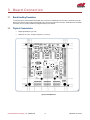
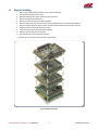
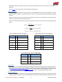
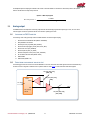
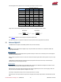
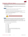
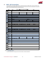
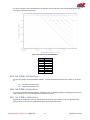
1
DM35425HR PCI Express Data Acquisition Board User’s Manual BDM-610010047 Rev D Revision History Rev A Rev B Rev C Rev D Initial Release Add Parallel Bus set up note Add Power Consumption Updated IDAN Dimensions Picture Added a Channel Delay Section Added Equation 1 Corrected Signal Names in IDAN Pin Out Update Register Map to FPGA Rev C i. ADC Function Block changed to 0x01031000 ii. DAC Function Block changed to 0x01032000 iii. ADIO Function Block changed to 0x01003001 iv. Add CH_FIFO_ACCESS register to ADC, DAC and ADIO Add Section 5.6 External Clocking Add Clock Source description RTD Embedded Technologies, Inc. 103 Innovation Boulevard State College, PA 16803 USA Telephone: 814-234-8087 Fax: 814-234-5218 www.rtd.com [email protected] [email protected] Advanced Analog I/O, Advanced Digital I/O, aAIO, aDIO, a2DIO, Autonomous SmartCal, “Catch the Express”, cpuModule, dspFramework, dspModule, expressMate, ExpressPlatform, HiDANplus, “MIL Value for COTS prices”, multiPort, PlatformBus, and PC/104EZ are trademarks, and “Accessing the Analog World”, dataModule, IDAN, HiDAN, RTD, and the RTD logo are registered trademarks of RTD Embedded Technologies, Inc (formerly Real Time Devices, Inc.). PS/2 is a trademark of International Business Machines Inc. PCI, PCI Express, and PCIe are trademarks of PCI-SIG. PC/104, PC/104-Plus, PCI-104, PCIe/104, PCI/104-Express and 104 are trademarks of the PC/104 Embedded Consortium. All other trademarks appearing in this document are the property of their respective owners. Failure to follow the instructions found in this manual may result in damage to the product described in this manual, or other components of the system. The procedure set forth in this manual shall only be performed by persons qualified to service electronic equipment. Contents and specifications within this manual are given without warranty, and are subject to change without notice. RTD Embedded Technologies, Inc. shall not be liable for errors or omissions in this manual, or for any loss, damage, or injury in connection with the use of this manual. Copyright © 2015 by RTD Embedded Technologies, Inc. All rights reserved. RTD Embedded Technologies, Inc. | www.rtd.com ii DM35425HR User’s Manual Table of Contents 1 2 3 4 5 Introduction 8 1.1 Product Overview........................................................................................................................................................................ 8 1.2 Board features ............................................................................................................................................................................ 8 1.3 Ordering Information ................................................................................................................................................................... 8 1.4 Contact Information .................................................................................................................................................................... 8 1.4.1 Sales Support 8 1.4.2 Technical Support 9 Specifications 10 2.1 Operating Conditions ................................................................................................................................................................ 10 2.2 Electrical Characteristics .......................................................................................................................................................... 10 2.2.1 Analog Input FFT plots 12 2.2.2 Analog input histograms 12 Board Connection 13 3.1 Board Handling Precautions ..................................................................................................................................................... 13 3.2 Physical Characteristics ............................................................................................................................................................ 13 3.3 Connectors and Jumpers .......................................................................................................................................................... 14 3.3.1 Bus Connectors 14 CN1(Top) & CN2(Bottom): PCIe Connector 14 3.3.2 DM35425 External I/O Connectors 15 CN3 & CN4: Analog/Digital I/O Connector 15 Other Connectors 16 3.3.3 Jumpers 16 3.4 Steps for Installing .................................................................................................................................................................... 17 IDAN Connections 18 4.1 Module Handling Precautions ................................................................................................................................................... 18 4.2 Physical Characteristics ............................................................................................................................................................ 18 4.3 Connectors................................................................................................................................................................................ 18 4.3.1 Bus Connectors 18 CN1(Top) & CN2(Bottom): PCIe Connector 18 4.4 Connectors................................................................................................................................................................................ 19 4.4.1 External I/O Connectors 19 P2 Connector - 68-pin Subminiature “D” Female Connector 19 P3 Connector - 68-pin Subminiature “D” Female Connector 20 P2 Connector - 62-pin High Density “D” Female Connector 21 P3 Connector - 62-pin High Density “D” Female Connector 22 4.5 Steps for Installing .................................................................................................................................................................... 23 Functional Description 24 5.1 Block Diagram........................................................................................................................................................................... 24 5.2 Control Interface with DMA Engine........................................................................................................................................... 24 5.3 Analog input .............................................................................................................................................................................. 24 5.3.1 Initialization 25 5.3.2 Simplified block diagram of analog input 25 Single-Ended Input Mode 25 Differential Input Mode 25 Full-Scale Input Range 25 Bipolar/Unipolar Mode 26 RTD Embedded Technologies, Inc. | www.rtd.com iii DM35425HR User’s Manual Channel Delay Effective Sampling Rate 6 26 26 5.4 Analog output ............................................................................................................................................................................ 27 5.4.1 Initializing the DAC Converter 27 5.4.2 Simplified block diagram of analog output 27 5.5 Advanced Digital I/O ................................................................................................................................................................. 28 DMA 28 Advanced Interrupts 28 Parallel Bus Mode 28 5.6 External Clocking ...................................................................................................................................................................... 29 Register Address Space Register Types Clock Source 30 30 30 6.1 BAR0 – General Board Control ................................................................................................................................................ 31 6.1.1 GBC_BRD_RST (Read/Write) 31 6.1.2 GBC_EOI (Read/Clear) 31 6.1.3 GBC_REV (Read-Only) 31 6.1.4 GBC_FMT (Read-Only) 31 6.1.5 GBC_PDP (Read-Only) 31 6.1.6 GBC_BUILD (Read-Only) 31 6.1.7 GBC_SYS_CLK_FREQ (Read Only) 32 6.1.8 GBC_IRQ_STATUS (Read/Clear) 32 6.1.9 GBC_DIRQ_STATUS (Read/Clear) 32 6.1.10 FBn_ID (Read-Only) 32 6.1.11 FBn_Offset (Read-Only) 32 6.1.12 FBn_Offset_DMA (Read-Only) 32 6.2 BAR2 – Functional Block Standard DMA ................................................................................................................................. 33 6.2.1 FB_DMAm_Action (Read/Write) 33 6.2.2 FB_DMAm_LAST_ACTION (READ/WRITE) 33 6.2.3 FB_DMAm_Setup (Read/Write) 34 6.2.4 FB_DMAm_Stat_Used (Read/Write) 34 6.2.5 FB_DMAm_Stat_Invalid (Read/Write) 34 6.2.6 FB_DMAm_Stat_Overflow (Read/Write) 34 6.2.7 FB_DMAm_Stat_Underflow (Read/Write) 34 6.2.8 FB_DMAm_Stat_Complete (Read/Write) 34 6.2.9 FB_DMAm_Current_Buffer (Read-Only) 34 6.2.10 FB_DMAm_COUNT (Read-Only) 34 6.2.11 FB_DMAm_RD_FIFO_CNT (Read-Only) 34 6.2.12 FB_DMAm_WR_FIFO_CNT (Read-Only) 35 6.2.13 FB_DMAm_ADDRESSn (Read/Write) 35 6.2.14 FB_DMAm_SIZEn (Read/Write) 35 6.2.15 FB_DMAm_CTRLn (Read/Write) 35 6.2.16 FB_DMAm_STATn (Read/Clear) 35 6.3 BAR2 – ADC Functional Block ................................................................................................................................................. 36 6.3.1 FB_ID (Read-Only) 36 6.3.2 FB_DMA_CHANNELS (Read -Only) 37 6.3.3 FB_DMA_BUFFERS (Read-Only) 37 6.3.4 Mode_Status (Read/Write, Read-Only) 37 6.3.5 CLK_SRC (Read/Write) 37 6.3.6 START_TRIG (Read/Write) 37 6.3.7 STOP_TRIG (Read/Write) 37 6.3.8 CLK_DIV (Read/Write) 37 6.3.9 CLK_DIV_CNTR (Read Only) 38 6.3.10 PRE_TRIGGER_CAPTURE (Read/Write) 38 6.3.11 POST_STOP_CAPTURE (Read/Write) 38 6.3.12 SAMPLE_CNT (Read Only) 38 6.3.13 INT_ENA (Maskable Read/Write) 38 6.3.14 INT_STAT (Read/Clear) 38 6.3.15 CLK_SRC_GBLn 38 6.3.16 CHn_FRONT_END_CONFIG (Maskable Read/Write) 39 6.3.17 CHn_FIFO_DATA_CNT (Read) 39 6.3.18 CHn_FILTER (Read/Write) 39 RTD Embedded Technologies, Inc. | www.rtd.com iv DM35425HR User’s Manual 6.3.19 6.3.20 6.3.21 6.3.22 6.3.23 6.3.24 CHn_THRESH_STAT(Read/Clear) CHn_THRESH_ENA (Read/Write) CHn_THRESH_LOW (Read/Write) CHn_THRESH_HIGH (Read/Write) CHn_LAST_SAMPLE (Read-Only) CH_FIFO_ACCESS (Read/Write) 40 40 40 41 41 41 6.4 BAR2 – DAC Functional Block ................................................................................................................................................. 42 6.4.1 FB_ID (Read-Only) 42 6.4.2 FB_DMA_CHANNELS (Read -Only) 42 6.4.3 FB_DMA_BUFFERS (Read-Only) 42 6.4.4 Mode_Status (Read/Write, Read-Only) 42 6.4.5 CLK_SRC (Read/Write) 43 6.4.6 START_TRIG (Read/Write) 43 6.4.7 STOP_TRIG (Read/Write) 43 6.4.8 CLK_DIV (Read/Write) 43 6.4.9 CLK_DIV_CNTR (Read Only) 43 6.4.10 POST_STOP_CONVERSIONS (Read/Write) 43 6.4.11 CONVERSION_CNT (Read Only) 43 6.4.12 INT_ENA (Maskable Read/Write) 44 6.4.13 INT_STAT (Read/Clear) 44 6.4.14 CLK_SRC_GBLn 44 6.4.15 CH_FRONT_END_CONFIG (Maskable Read/Write) 44 6.4.16 CHn_FIFO_DATA_CNT (Read) 44 6.4.17 CH_MARKER_STAT(Read/Clear) 45 6.4.18 CH_MARKER_ENA (Read/Write) 45 6.4.19 CH_LAST_CONVERSION (Read/Write) 45 6.4.20 CH_FIFO_ACCESS (Read/Write) 45 6.5 BAR2 – Advanced Digital I/O Functional Block ........................................................................................................................ 46 6.5.1 FB_ID (Read-Only) 46 6.5.2 FB_DMA_CHANNELS (Read -Only) 46 6.5.3 FB_DMA_BUFFERS (Read-Only) 46 6.5.4 Mode_Status (Read/Write, Read-Only) 46 6.5.5 CLK_SRC (Read/Write) 47 6.5.6 START_TRIG (Read/Write) 47 6.5.7 STOP_TRIG (Read/Write) 47 6.5.8 CLK_DIV (Read/Write) 47 6.5.9 CLK_DIV_CNTR (Read Only) 47 6.5.10 PRE_TRIGGER_CAPTURE (Read/Write) 48 6.5.11 POST_STOP_CAPTURE (Read/Write) 48 6.5.12 SAMPLE_CNT (Read Only) 48 6.5.13 INT_ENA (Maskable Read/Write) 48 6.5.14 INT_STAT (Read/Clear) 48 6.5.15 CLK_SRC_GBLn 48 6.5.16 DIO_INPUT (Read Only) 49 6.5.17 DIO_OUTPUT (Read/Write) 49 6.5.18 DIO_DIRECTION (Read/Write) 49 6.5.19 ADV_INT_MODE (Read/Write) 50 6.5.20 ADV_INT_MASK (Read/Write) 50 6.5.21 ADV_INT_COMP (Read/Write) 50 6.5.22 ADV_INT_CAPT (Read/Write) 50 6.5.23 P_BUS_EN (Read/Write) 50 6.5.24 P_BUS_READY_EN (Read/Write) 50 6.5.25 CH_FIFO_ACCESS (Read/Write) 50 6.6 BAR2 – External Clocking Functional Block ............................................................................................................................. 51 6.6.1 FB_ID (Read-Only) 51 6.6.2 FB_DMA_CHANNELS (Read -Only) 51 6.6.3 FB_DMA_BUFFERS (Read-Only) 51 6.6.4 EXT_CLK_IN (Read-Only) 51 6.6.5 EXT_CLK_GATE_IN (Read Only) 51 6.6.6 EXT_CLK_DIR (Read/Write) 51 6.6.7 EXT_CLK_EDGE (Read/Write) 52 6.6.8 EXT_CLK_PWn (Read/Write) 52 6.6.9 EXT_CLKn_CFG (Read/Write) 52 RTD Embedded Technologies, Inc. | www.rtd.com v DM35425HR User’s Manual 7 Calibration 53 7.1 Required Equipment ................................................................................................................................................................. 53 7.2 ADC Calibration ........................................................................................................................................................................ 54 7.2.1 Bipolar Calibration 54 Bipolar Range Adjustment: -5 to +5 V 54 Bipolar Range Adjustment: -10 to +10 V 54 Bipolar Range Ideal Bit Weight 54 7.2.2 Unipolar Calibration 54 Unipolar Range Ideal Bit Weight 55 7.2.3 Gain Adjustment 55 7.3 DAC Calibration ........................................................................................................................................................................ 56 8 Troubleshooting 57 9 Additional Information 58 9.1 PC/104 Specifications ............................................................................................................................................................... 58 9.2 PCI and PCI Express Specification .......................................................................................................................................... 58 10 Limited Warranty 59 Table of Figures Figure 1: Channel FFT ............................................................................................................................................................................................ 12 Figure 2: Histogram ................................................................................................................................................................................................ 12 Figure 3: Board Dimensions ................................................................................................................................................................................... 13 Figure 4: Board Connections .................................................................................................................................................................................. 14 Figure 5: Example 104™Stack ............................................................................................................................................................................... 17 Figure 6: IDAN Dimensions .................................................................................................................................................................................... 18 Figure 7: Example IDAN System ............................................................................................................................................................................ 23 Figure 8: DM35425 Block Diagram......................................................................................................................................................................... 24 Figure 9: Filter Response with each ORDER Value ............................................................................................................................................... 40 Figure 10: DM35425HR Trimpots ........................................................................................................................................................................... 53 Table of Tables Table 1: Ordering Options ........................................................................................................................................................................................ 8 Table 2: Operating Conditions ................................................................................................................................................................................ 10 Table 3: Electrical Characteristics .......................................................................................................................................................................... 10 Table 4: CN3 Differential Mode Pin-out .................................................................................................................................................................. 15 Table 5: CN3 Single-Ended Mode Pin-out.............................................................................................................................................................. 15 Table 6: CN4 Differential Mode Pin-out .................................................................................................................................................................. 16 Table 7: CN4 Single-Ended Mode Pin-out.............................................................................................................................................................. 16 Table 8: IDAN- DM35425 68-Pin Subminiature "D" Connector .............................................................................................................................. 19 Table 9: IDAN- DM35425 68-Pin Subminiature "D" Connector .............................................................................................................................. 20 Table 10: IDAN- DM35425 62-Pin High Density "D" Connector............................................................................................................................. 21 Table 11: IDAN- DM35425 62-Pin High Density "D" Connector............................................................................................................................. 22 Table 12: ADC Bipolar Code ( ±5 V Input Range) ................................................................................................................................................. 26 Table 13: ADC Bipolar Code ( ±10 V Input Range) ............................................................................................................................................... 26 Table 14: ADC Unipolar Code ( 0 to 10 V Input Range)......................................................................................................................................... 26 Table 15: BAR0 Registers ...................................................................................................................................................................................... 31 Table 16: DMA Registers ........................................................................................................................................................................................ 33 Table 17: Multi-Channel ADC Functional Block ..................................................................................................................................................... 36 Table 18: ADC Full-Scale Settings ......................................................................................................................................................................... 39 Table 19: Multi-Channel DAC Functional Block ..................................................................................................................................................... 42 RTD Embedded Technologies, Inc. | www.rtd.com vi DM35425HR User’s Manual Table 20: DAC Full-Scale Settings ......................................................................................................................................................................... 44 Table 21: Digital I/O Functional Block..................................................................................................................................................................... 46 Table 22:External Clocking Functional Block ......................................................................................................................................................... 51 Table 23: Data Values for Calibrating Bipolar 10 V Range .................................................................................................................................... 54 Table 24: Data Values for Calibrating Bipolar 20 V Range .................................................................................................................................... 54 Table 25: ADC Bit Weights, Bipolar ........................................................................................................................................................................ 54 Table 26: Data Values for Calibrating Bipolar 20 V Range .................................................................................................................................... 55 Table 27: ADC Bit Weights, Unipolar...................................................................................................................................................................... 55 Table 28: Trimpots for Calibrating ADC Gain ......................................................................................................................................................... 55 Table 29: DAC Bit Weights ..................................................................................................................................................................................... 56 Table 30: Trimpots for Calibrating DAC Gain ......................................................................................................................................................... 56 RTD Embedded Technologies, Inc. | www.rtd.com vii DM35425HR User’s Manual 1 Introduction 1.1 Product Overview The DM35425 is a software configurable high-speed, 12-bit data acquisition module in the PCIe/104 format. This module provides 16 differential or 32 single-ended analog input channels, with programmable gain and input ranges. The DM35425 also features four 12-bit highspeed analog outputs with programmable output ranges, and a 32-bit port of digital I/O. 1.2 Board features 1.3 PCIe x 1 Interface o Universal Board can be used with a PCIe/104 Type 1 or Type 2 host o Dedicated DMA channel per I/O for maximum efficiency Analog inputs: o 16 Differential or 32 Single-ended analog input channels o 1.25 MSPS maximum input sampling rate o 12 bits resolution o Programmable single ended or differential inputs per channels o Threshold detection can generate an interrupt, or be used as a start or stop trigger o Configurable IIR filter on each channel Analog outputs: o 4 channels high-speed o 12 bit D/A converters o ±5, +5, ±10, & +10V output ranges o 7 µs full-scale settling time Advanced Digital I/O o 32-bit port of digital I/O o Bit programmable direction o Advanced digital interrupts o Parallel Bus Mode External Clocking o Provides 6 external clocking pins that can be used as inputs or outputs o Provides external triggering o External gate for each clock pin Ordering Information The DM35425 is available with the following options: Table 1: Ordering Options Part Number DM35425HR IDAN-DM35425HR-62S IDAN-DM35425HR-68S Description PCIe/104 Analog I/O dataModule PCIe/104 Analog I/O dataModule in IDAN enclosure with 62-pin D-Sub Connector PCIe/104 Analog I/O dataModule in IDAN enclosure with 68-pin High-Density Connector The Intelligent Data Acquisition Node (IDAN™) building block can be used in just about any combination with other IDAN building blocks to create a simple but rugged 104™ stack. This module can also be incorporated in a custom-built RTD HiDAN™ or HiDANplus High Reliability Intelligent Data Acquisition Node. Contact RTD sales for more information on our high reliability systems. 1.4 Contact Information 1.4.1 SALES SUPPORT For sales inquiries, you can contact RTD Embedded Technologies sales via the following methods: RTD Embedded Technologies, Inc. | www.rtd.com 8 DM35425HR User’s Manual Phone: E-Mail: 1.4.2 1-814-234-8087 [email protected] Monday through Friday, 8:00am to 5:00pm (EST). TECHNICAL SUPPORT If you are having problems with you system, please try the steps in the Troubleshooting section of this manual on page 57. For help with this product, or any other product made by RTD, you can contact RTD Embedded Technologies technical support via the following methods: Phone: E-Mail: 1-814-234-8087 Monday through Friday, 8:00am to 5:00pm (EST). [email protected] RTD Embedded Technologies, Inc. | www.rtd.com 9 DM35425HR User’s Manual 2 Specifications 2.1 Operating Conditions Table 2: Operating Conditions 2.2 Symbol Vcc5 Vcc3 Vcc12 Vcc-12 Ta Ts RH Parameter 5V Supply Voltage 3.3V Supply Voltage 12V Supply Voltage -12V Supply Voltage Operating Temperature Storage Temperature Relative Humidity MTBF Mean Time Before Failure Test Condition Non-Condensing Telcordia Issue 2 30°C, Ground benign, controlled Min 4.75 n/a n/a n/a -40 -55 0 Max 5.25 n/a n/a n/a +70 +125 90% TBD Unit V V V V C C % Hours Electrical Characteristics Table 3: Electrical Characteristics Symbol P Icc5 Parameter Power Consumption 5V Input Supply Current Test Condition Vcc5 = 5.0V Active PCIe/104 Bus Min Differential Output Voltage DC Differential TX Impedance Differential Input Voltage DC Differential RX Impedance Electrical Idle Detect Threshold FSR Linear Input Voltage Full-Scale Differential Input Voltage Resolution Data Rate Input Impedance ENOB SNR SINAD THD SFDR Third Order Intermodulation Noise Free Bits Channel to Channel Cross Talk G Typical 0.8 80 0.175 80 65 RTD Embedded Technologies, Inc. | www.rtd.com Unit W A 1.2 120 1.2 120 175 Analog to Digital Converter IN+ or IN-10 −5 VIN=(IN+ -IN-) G = PGA Gain 𝐺 Inputs= 0.8dBFS @ 10Khz Single-Ended, ±5V Inputs= 0.8dBFS @ 10Khz Single-Ended, ±5V Inputs= 0.8dBFS @ 10Khz Single-Ended, ±5V Inputs= 0.8dBFS @ 10Khz Single-Ended, ±5V Inputs= 0.8dBFS @ 10Khz Single-Ended, ±5V FIN1=0.8dBFS @ 10.0708Khz FIN2=0.8dBFS @ 39.0625Khz Inputs Grounded Differential Inputs, ±5V No Channel Delay ½ Sample Delay Sample Delay 2 Sample Delay +10 4.99878 𝐺 12 1.25 >6 V Ω V Ω mV V V 11.55 Bits MSPS MΩ Bits 70.54 dB 70.44 dB -86.78 dB 89.50 dB 83.4 dB 11 Bits -20.46 -41.68 -59.54 -66.41 Gains Full-Scale Analog Output Voltage Max 4.35 0.87 dB dB dB dB 0.5,1,2,4,8 Digital to Analog Converter G=1 10 -5 4.99756 V DM35425HR User’s Manual Table 3: Electrical Characteristics Symbol G Parameter Resolution Relative Accuracy Gain Error Settling Time Output Current Slew Rate Gains Output Impedance Test Condition Min Typical Max 12 ±1 ±2 5 5 2 Unit Bits LSB LSB µs mA V/µs 1,2 45 Ω Digital I/O VIL VIH VOL VOH Input High Voltage Input Low Voltage Output Low Voltage Output High Voltage 5V Output RTD Embedded Technologies, Inc. | www.rtd.com 2 -0.5 0.0 2.6 IO = 12mA IO = -12mA CN3, CN4 11 5.5 0.8 0.4 3.3 200 V V V V mA DM35425HR User’s Manual 2.2.1 ANALOG INPUT FFT PLOTS In Figure 1, a coherent 10 kHz sine wave signal was attached to input Channel 0 in the +/-5V, Single-ended mode. The FFT absolute value was calculated using 8192 data sample. 0 -20 dBFS -40 -60 ADC Noise Floor -80 -100 -120 -140 0 100 200 300 400 500 600 Frequency (kHz) Figure 1: Channel FFT 2.2.2 ANALOG INPUT HISTOGRAMS In Figure 2 you can see a histogram of samples from sampling a grounded input in +/-10 V, differential input range. The number of samples is 32768. 30000 Frequency 25000 20000 15000 10000 5000 0 -1 0 1 Bin Figure 2: Histogram RTD Embedded Technologies, Inc. | www.rtd.com 12 DM35425HR User’s Manual 3 Board Connection 3.1 Board Handling Precautions To prevent damage due to Electrostatic Discharge (ESD), keep your board in its antistatic bag until you are ready to install it into your system. When removing it from the bag, hold the board at the edges, and do not touch the components or connectors. Handle the board in an antistatic environment, and use a grounded workbench for testing and handling of your hardware. 3.2 Physical Characteristics Weight: Approximately 55 g (0.12 lbs.) Dimensions: 90.17 mm L x 95.89 mm W (3.550 in L x 3.775 in W) Figure 3: Board Dimensions RTD Embedded Technologies, Inc. | www.rtd.com 13 DM35425HR User’s Manual 3.3 Connectors and Jumpers CN3: Analog/Digital I/O CN3: Analog/Digital I/O CN1 & CN2: PCIe Connector Figure 4: Board Connections 3.3.1 BUS CONNECTORS CN1(Top) & CN2(Bottom): PCIe Connector The PCIe connector is the connection to the system CPU. The position and pin assignments are compliant with the PCI/104-Express Specification. (See PC/104 Specifications on page 58) The DM35425 is a “Universal” board, and can connect to either a Type 1 or Type 2 PCIe/104 connector. RTD Embedded Technologies, Inc. | www.rtd.com 14 DM35425HR User’s Manual 3.3.2 DM35425 EXTERNAL I/O CONNECTORS CN3 & CN4: Analog/Digital I/O Connector The Digital I/O Connector is a 2 x 25, 0.1” spacing right-angle connector. The pin assignments are shown in Tables below. Table 4: CN3 Differential Mode Pin-out AIN0+ AIN1+ AIN2+ AIN3+ AIN4+ AIN5+ AIN6+ AIN7+ AOUT0 AOUT1 AGND DIO7 DIO6 DIO5 DIO4 DIO3 DIO2 DIO1 DIO0 EXT_CLK_2 EXT_CLK_3 EXT_CLK_5 EXT_CLK_7 Reserved Reserved 1 3 5 7 9 11 13 15 17 19 21 23 25 27 29 31 33 35 37 39 41 43 45 47 49 2 4 6 8 10 12 14 16 18 20 22 24 26 28 30 32 34 36 38 40 42 44 46 48 50 Table 5: CN3 Single-Ended Mode Pin-out AIN0AIN1AIN2AIN3AIN4AIN5AIN6AIN7AGND AGND AGND DIO15 DIO14 DIO13 DIO12 DIO11 DIO10 DIO9 DIO8 GND EXT_CLK_4 EXT_CLK_6 Reserved +5V GND RTD Embedded Technologies, Inc. | www.rtd.com AIN0 AIN1 AIN2 AIN3 AIN4 AIN5 AIN6 AIN7 AOUT0 AOUT1 AGND DIO7 DIO6 DIO5 DIO4 DIO3 DIO2 DIO1 DIO0 EXT_CLK_2 EXT_CLK_3 EXT_CLK_5 EXT_CLK_7 Reserved Reserved 15 1 3 5 7 9 11 13 15 17 19 21 23 25 27 29 31 33 35 37 39 41 43 45 47 49 2 4 6 8 10 12 14 16 18 20 22 24 26 28 30 32 34 36 38 40 42 44 46 48 50 AIN8 AIN9 AIN10 AIN11 AIN12 AIN13 AIN14 AIN15 AGND AGND AGND DIO15 DIO14 DIO13 DIO12 DIO11 DIO10 DIO9 DIO8 GND EXT_CLK_4 EXT_CLK_6 Reserved +5V GND DM35425HR User’s Manual Table 6: CN4 Differential Mode Pin-out AIN8+ AIN9+ AIN10+ AIN11+ AIN12+ AIN13+ AIN14+ AIN15+ AOUT2 AOUT3 AGND DIO23 DIO22 DIO21 DIO20 DIO19 DIO18 DIO17 DIO16 EXT_CLK_GATE2 EXT_CLK_GATE3 EXT_CLK_GATE5 EXT_CLK_GATE7 Reserved Reserved 1 3 5 7 9 11 13 15 17 19 21 23 25 27 29 31 33 35 37 39 41 43 45 47 49 2 4 6 8 10 12 14 16 18 20 22 24 26 28 30 32 34 36 38 40 42 44 46 48 50 Table 7: CN4 Single-Ended Mode Pin-out AIN8AIN9AIN10AIN11AIN12AIN13AIN14AIN15AGND AGND AGND DIO31 DIO30 DIO29 DIO28 DIO27 DIO26 DIO25 DIO24 GND EXT_CLK_GATE4 EXT_CLK_GATE6 Reserved +5V GND AIN16 AIN17 AIN18 AIN19 AIN20 AIN21 AIN22 AIN23 AOUT2 AOUT3 AGND DIO23 DIO22 DIO21 DIO20 DIO19 DIO18 DIO17 DIO16 EXT_CLK_GATE2 EXT_CLK_GATE3 EXT_CLK_GATE5 EXT_CLK_GATE7 Reserved Reserved 1 3 5 7 9 11 13 15 17 19 21 23 25 27 29 31 33 35 37 39 41 43 45 47 49 2 4 6 8 10 12 14 16 18 20 22 24 26 28 30 32 34 36 38 40 42 44 46 48 50 AIN24 AIN25 AIN26 AIN27 AIN28 AIN29 AIN30 AIN31 AGND AGND AGND DIO31 DIO30 DIO29 DIO28 DIO27 DIO26 DIO25 DIO24 GND EXT_CLK_GATE4 EXT_CLK_GATE6 Reserved +5V GND Other Connectors CN5 and CN6 are for Factory Use only 3.3.3 JUMPERS There are no jumpers on the board. RTD Embedded Technologies, Inc. | www.rtd.com 16 DM35425HR User’s Manual 3.4 Steps for Installing 1. 2. 3. 4. 5. 6. 7. 8. 9. 10. 11. 12. Always work at an ESD protected workstation, and wear a grounded wrist-strap. Turn off power to the PC/104 system or stack. Select and install stand-offs to properly position the module on the stack. Remove the module from its anti-static bag. Check that pins of the bus connector are properly positioned. Check the stacking order; make sure all of the busses used by the peripheral cards are connected to the cpuModule. Hold the module by its edges and orient it so the bus connector pins line up with the matching connector on the stack. Gently and evenly press the module onto the PC/104 stack. If any boards are to be stacked above this module, install them. Attach any necessary cables to the PC/104 stack. Re-connect the power cord and apply power to the stack. Boot the system and verify that all of the hardware is working properly. Figure 5: Example 104™Stack RTD Embedded Technologies, Inc. | www.rtd.com 17 DM35425HR User’s Manual 4 IDAN Connections 4.1 Module Handling Precautions To prevent damage due to Electrostatic Discharge (ESD), keep your module in its antistatic bag until you are ready to install it into your system. When removing it from the bag, hold the module by the aluminum enclosure, and do not touch the components or connectors. Handle the module in an antistatic environment, and use a grounded workbench for testing and handling of your hardware. 4.2 Physical Characteristics Weight: Approximately 0.33 Kg (0.72 lbs.) Dimensions: 151.972 mm L x 129.978 mm W x 34.011 mm H (5.983 in L x 5.117 in W x 1.339 in H) Figure 6: IDAN Dimensions 4.3 Connectors 4.3.1 BUS CONNECTORS CN1(Top) & CN2(Bottom): PCIe Connector The PCIe connector is the connection to the system CPU. The position and pin assignments are compliant with the PCI/104-Express Specification. (See PC/104 Specifications on page 58) The DM35425 is a “Universal” board, and can connect to either a Type 1 or Type 2 PCIe/104 connector. RTD Embedded Technologies, Inc. | www.rtd.com 18 DM35425HR User’s Manual 4.4 Connectors 4.4.1 EXTERNAL I/O CONNECTORS P2 Connector - 68-pin Subminiature “D” Female Connector Connector Part #: Amp 749070-7 Sample Mating Connector: Amp Table 8: IDAN- DM35425 68-Pin Subminiature "D" Connector IDAN Pin# 1 2 3 4 5 6 7 8 9 10 11 12 13 4 15 16 17 18 19 20 21 22 23 24 25 26 27 28 29 30 31 32 33 34 Signal AIN0+/AIN0 AIN0-/AIN8 AIN1+/AIN1 AIN1-/AIN9 AIN2+/AIN2 AIN2-/AIN10 AIN3+/AIN3 AIN3-/AIN11 AIN4+/AIN4 AIN4-/AIN12 AIN5+/AIN5 AIN5-/AIN13 AIN6+/AIN6 AIN6-/AIN14 AIN7+/AIN7 AIN7-/AIN15 AOUT0 AGND AOUT1 AGND AGND AGND DIO7 DIO15 DIO6 DIO14 DIO5 DIO13 DIO4 DIO12 DIO3 DIO11 DIO2 DIO10 CN3 CN3 CN3 CN3 CN3 CN3 CN3 CN3 CN3 CN3 CN3 CN3 CN3 CN3 CN3 CN3 CN3 CN3 CN3 CN3 CN3 CN3 CN3 CN3 CN3 CN3 CN3 CN3 CN3 CN3 CN3 CN3 CN3 CN3 Table 8: IDAN- DM35425 68-Pin Subminiature "D" Connector DM35425 Pin # 1 2 3 4 5 6 7 8 9 10 11 12 13 14 15 16 17 18 19 20 21 22 23 24 25 26 27 28 29 30 31 32 33 34 RTD Embedded Technologies, Inc. | www.rtd.com 786090-7(IDC Crimp) IDAN Pin# 35 36 37 38 39 40 41 42 43 44 45 46 47 48 49 50 51 52 53 54 55 56 57 58 59 60 61 62 63 64 65 66 67 68 19 Signal DIO1 DIO9 DIO0 DIO8 EXT_CLK_2 GND EXT_CLK_3 EXT_CLK_4 EXT_CLK_5 EXT_CLK_6 EXT_CLK_7 Reserved Reserved +5V Reserved GND N/C N/C N/C N/C N/C N/C N/C N/C N/C N/C N/C N/C N/C N/C N/C N/C N/C N/C CN3 CN3 CN3 CN3 CN3 CN3 CN3 CN3 CN3 CN3 CN3 CN3 CN3 CN3 CN3 CN3 DM35425 Pin # 35 36 37 38 39 40 41 42 43 44 45 46 47 48 49 50 DM35425HR User’s Manual P3 Connector - 68-pin Subminiature “D” Female Connector Connector Part #: Amp 749070-7 Sample Mating Connector: Amp Table 9: IDAN- DM35425 68-Pin Subminiature "D" Connector IDAN Pin# 1 2 3 4 5 6 7 8 9 10 11 12 13 4 15 16 17 18 19 20 21 22 23 24 25 26 27 28 29 30 31 32 33 34 Signal AIN8+/AIN16 AIN8-/AIN24 AIN9+/AIN17 AIN9-/AIN25 AIN10+/AIN18 AIN10-/AIN26 AIN11+/AIN19 AIN11-/AIN27 AIN12+/AIN20 AIN12-/AIN28 AIN13+/AIN21 AIN13-/AIN29 AIN14+/AIN22 AIN14-/AIN30 AIN15+/AIN23 AIN15-/AIN31 AOUT2 AGND AOUT3 AGND AGND AGND DIO23 DIO31 DIO22 DIO30 DIO21 DIO29 DIO20 DIO28 DIO19 DIO27 DIO18 DIO26 CN4 CN4 CN4 CN4 CN4 CN4 CN4 CN4 CN4 CN4 CN4 CN4 CN4 CN4 CN4 CN4 CN4 CN4 CN4 CN4 CN4 CN4 CN4 CN4 CN4 CN4 CN4 CN4 CN4 CN4 CN4 CN4 CN4 CN4 Table 8: IDAN- DM35425 68-Pin Subminiature "D" Connector DM35425 Pin # 1 2 3 4 5 6 7 8 9 10 11 12 13 14 15 16 17 18 19 20 21 22 23 24 25 26 27 28 29 30 31 32 33 34 RTD Embedded Technologies, Inc. | www.rtd.com 786090-7(IDC Crimp) IDAN Pin# 35 36 37 38 39 40 41 42 43 44 45 46 47 48 49 50 51 52 53 54 55 56 57 58 59 60 61 62 63 64 65 66 67 68 20 Signal DIO17 DIO25 DIO16 DIO24 EXT_CLK_GATE2 GND EXT_CLK_GATE3 EXT_CLK_GATE4 EXT_CLK_GATE5 EXT_CLK_GATE6 EXT_CLK_GATE7 Reserved Reserved +5V Reserved GND N/C N/C N/C N/C N/C N/C N/C N/C N/C N/C N/C N/C N/C N/C N/C N/C N/C N/C CN4 CN4 CN4 CN4 CN4 CN4 CN4 CN4 CN4 CN4 CN4 CN4 CN4 CN4 CN4 CN4 DM35425 Pin # 35 36 37 38 39 40 41 42 43 44 45 46 47 48 49 50 DM35425HR User’s Manual P2 Connector - 62-pin High Density “D” Female Connector Connector Part #: VALCONN HDB-62S Sample Mating Connector: VALCONN Table 10: IDAN- DM35425 62-Pin High Density "D" Connector IDAN Pin# 1 2 3 4 5 6 7 8 9 10 11 12 13 14 15 16 17 18 19 20 21 22 23 24 25 26 27 28 29 30 31 Signal AIN0+/AIN0 AIN1-/AIN9 AIN3+/AIN3 AIN4-/AIN12 AIN6+/AIN6 AIN7-/AIN15 AOUT1 AGND DIO6 DIO13 DIO3 DIO10 DIO0 GND EXT_CLK_5 Reserved Reserved AIN0-/AIN8 AIN2+/AIN2 AIN3-/AIN11 AIN5+/AIN5 AIN6-/AIN14 AOUT0 AGND DIO7 DIO14 DIO4 Table 10: IDAN- DM35425 62-Pin High Density "D" Connector DM35425 Pin # CN3 1 CN3 4 CN3 7 CN3 10 CN3 13 CN3 16 CN3 19 CN3 22 CN3 25 CN3 28 CN3 31 CN3 34 CN3 37 CN3 40 CN3 43 CN3 46 CN3 49 Reserved Reserved Reserved Reserved CN3 2 CN3 5 CN3 8 CN3 11 CN3 14 CN3 17 CN3 20 CN3 23 CN3 26 CN3 29 RTD Embedded Technologies, Inc. | www.rtd.com HDB-62P IDAN Pin# 32 33 34 35 36 37 38 39 40 41 42 43 44 45 46 47 48 49 50 51 52 53 54 55 56 57 58 59 60 61 62 21 Signal DIO11 DIO1 DIO8 EXT_CLK_3 EXT_CLK_6 Reserved GND AIN1+/AIN1 AIN2-/AIN10 AIN4+/AIN4 AIN5-/AIN13 AIN7+/AIN7 AGND AGND DIO15 DIO5 DIO12 DIO2 DIO9 EXT_CLK_2 EXT_CLK_4 EXT_CLK_7 +5V DM35425 Pin # CN3 32 CN3 35 CN3 38 CN3 41 CN3 44 CN3 47 CN3 50 Reserved Reserved Reserved Reserved CN3 3 CN3 6 CN3 9 CN3 12 CN3 15 CN3 18 CN3 21 CN3 24 CN3 27 CN3 30 CN3 33 CN3 36 CN3 39 CN3 42 CN3 45 CN3 48 Reserved Reserved Reserved Reserved DM35425HR User’s Manual P3 Connector - 62-pin High Density “D” Female Connector Connector Part #: VALCONN HDB-62S Sample Mating Connector: VALCONN Table 11: IDAN- DM35425 62-Pin High Density "D" Connector IDAN Pin# 1 2 3 4 5 6 7 8 9 10 11 12 13 14 15 16 17 18 19 20 21 22 23 24 25 26 27 28 29 30 31 Signal AIN8+/AIN16 AIN9-/AIN25 AIN11+/AIN19 AIN12-/AIN28 AIN14+/AIN22 AIN15-/AIN31 AOUT3 AGND DIO22 DIO29 DIO19 DIO26 DIO16 GND EXT_CLK_GATE5 Reserved Reserved AIN8-/AIN24 AIN10+/AIN18 AIN11-/AIN27 AIN13+/AIN21 AIN14-/AIN30 AOUT2 AGND DIO23 DIO30 DIO20 Table 10: IDAN- DM35425 62-Pin High Density "D" Connector DM35425 Pin # CN4 1 CN4 4 CN4 7 CN4 10 CN4 13 CN4 16 CN4 19 CN4 22 CN4 25 CN4 28 CN4 31 CN4 34 CN4 37 CN4 40 CN4 43 CN4 46 CN4 49 Reserved Reserved Reserved Reserved CN4 2 CN4 5 CN4 8 CN4 11 CN4 14 CN4 17 CN4 20 CN4 23 CN4 26 CN4 29 RTD Embedded Technologies, Inc. | www.rtd.com HDB-62P IDAN Pin# 32 33 34 35 36 37 38 39 40 41 42 43 44 45 46 47 48 49 50 51 52 53 54 55 56 57 58 59 60 61 62 22 Signal DIO27 DIO17 DIO24 EXT_CLK_GATE3 EXT_CLK_GATE6 Reserved GND AIN9+/AIN17 AIN10-/AIN26 AIN12+/AIN20 AIN13-/AIN29 AIN15+/AIN23 AGND AGND DIO31 DIO21 DIO28 DIO18 DIO25 EXT_CLK_GATE2 EXT_CLK_GATE4 EXT_CLK_GATE7 +5V DM35425 Pin # CN4 32 CN4 35 CN4 38 CN4 41 CN4 44 CN4 47 CN4 50 Reserved Reserved Reserved Reserved CN4 3 CN4 6 CN4 9 CN4 12 CN4 15 CN4 18 CN4 21 CN4 24 CN4 27 CN4 30 CN4 33 CN4 36 CN4 39 CN4 42 CN4 45 CN4 48 Reserved Reserved Reserved Reserved DM35425HR User’s Manual 4.5 Steps for Installing 1. 2. 3. 4. 5. 6. 7. 8. 9. 10. 11. 12. Always work at an ESD protected workstation, and wear a grounded wrist-strap. Turn off power to the IDAN system. Remove the module from its anti-static bag. Check that pins of the bus connector are properly positioned. Check the stacking order; make sure all of the busses used by the peripheral cards are connected to the cpuModule. Hold the module by its edges and orient it so the bus connector pins line up with the matching connector on the stack. Gently and evenly press the module onto the IDAN system. If any boards are to be stacked above this module, install them. Finish assembling the IDAN stack by installing screws of an appropriate length. Attach any necessary cables to the IDAN system. Re-connect the power cord and apply power to the stack. Boot the system and verify that all of the hardware is working properly. Figure 7: Example IDAN System RTD Embedded Technologies, Inc. | www.rtd.com 23 DM35425HR User’s Manual 5 Functional Description 5.1 Block Diagram The Figure below shows the functional block diagram of the DM35425. The various parts of the block diagram are discussed in the following sections. PGA (0.5,1,2,4,8) AIN 31 Input Multiplexer PCIe x1 Control Interface With DMA Engine I/O Connector PCIe Bus … AIN 0 Analog input: 12 bit @1.25MSPS Analog Output: 12 bit @ 200KHz … DIO0 DIO31 Figure 8: DM35425 Block Diagram 5.2 Control Interface with DMA Engine The DM35425 features a FPGA with a built in PCI Express interface and DMA engine. The FPGA controls all communication between the bus and the control logic on the board. The FPGA also features small FIFOs for use with DMA, which is needed for continuous data transfer. Each DAC and ADC is provided with its own FIFO and DMA channel, allowing them to transfer data independent of one another. Each DMA channel can be programmed to transfer data from FPGA to PCIe bus or from the PCIe bus to the FPGA. Each DMA channel also features a 64-bit PCI addressing and can access a maximum 16MB of memory for buffers. 5.3 Analog input The DM35425 has 16 differential or 32 single-end channel inputs muxed to a single 12 bit SAR ADC converter, to provide high speed and high digital resolution of the analog input. The ADC converter has a max throughput of 1.25MHz (1 Channel). Refer to Equation 1 below to calculate max sampling rate. The high input impedance, low distortion, low noise operation design give you accurate results. The DM35425 also provides ±12V overvoltage input protection to the analog connector. The DM35425 has a programmable input. This provides the user the ability to select single-ended/differential input, full-scale input range, unipolar/bipolar input, and channel sampling delay. RTD Embedded Technologies, Inc. | www.rtd.com 24 DM35425HR User’s Manual Each ADC channel supports a 511 sample FIFO for DMA. Each sample packed into a 32 bits word. 5.3.1 INITIALIZATION There are several steps to initialize the Analog to Digital converter. The initialization prepares the converter and the front-end to capture samples. Following the example programs and using the drivers provided by RTD will ensure that these steps are followed in the correct order. Initialization of the ADC is performed as follows: 1. 2. 3. 4. 5. 6. 7. 8. 9. 10. 5.3.2 Set the ADC to the Uninitialized state (MODE = Uninitialized) Setup the DMA for the channel Set the input mode (CH_FRONT_END_CONFIG) Set the start and stop triggers (START_TRIG, STOP_TRIG) Set the clock source (CLK_SOURCE) Set the sample rate (CLK_DIV_CNTR) Set the Pre and/or Post Capture counters (PRE_TRIGGER_CAPTURE, POST_STOP_CAPTURE) Set the ADC to the Reset state (MODE = Reset) Start the DMA Start the ADC (MODE = Go) SIMPLIFIED BLOCK DIAGRAM OF ANALOG INPUT The following figure shows the front end circuit for the DM35425. It also shows the names of the FPGA registers in bold and the different ways the front-end can be configured for different modes of operation. Refer to section 6.3.16 for more information about FPGA registers. CHn_Front_End_Config [BIP_UNI] CHn_Front_End_Config [GAINSEL[2:0]] VREF Mux … AIN0/AIN0+ AIN1/AIN1+ AIN2/AIN2+ AIN3/AIN3+ IN+ PGA AIN28/AIN12AIN29/AIN13AIN30/AIN14AIN31/AIN15- IN- Data To FPGA Out ADC: 12 Bit @ 1.25 MSPS CHn_Front_End_Config [SE_DIFF] Single-Ended Input Mode In single-ended mode, the input signal is measured in reference to the boards GND. In this mode the input signal is connected to input AIN0 through AIN31, and the low side to any of the GND pins available on the Analog Connector. Differential Input Mode In this mode your signal source may or may not have a separate ground reference. In differential mode, the high side input is measured in reference to the low side input. In this mode you connect the high side of the input signal to the analog input, AIN0+ through AIN16+, and connect the low side to corresponding ADC - pin. In most cases, the board ground must still be attached to the device that is generating the input signal. When using the differential mode, you should install a 10 kΩ resistor pack at locations RN2 and RN18 on the DM35425HR to provide a reference to ground for signal sources without a separate ground reference. Full-Scale Input Range The DM35425 has a programmable gain input per channel. This gain can be programed for 1,2,4,8 to achieve input ranges ±5V, ±2.5V, ±1.25V, ±0.625V. RTD Embedded Technologies, Inc. | www.rtd.com 25 DM35425HR User’s Manual The DM35425 also features an attenuator in the front-end. This allows for additional input range of ±10V. This feature can only be used in bipolar mode. Refer to Table 18 on page 39 for full-scale ranges for both unipolar and bipolar modes. Bipolar/Unipolar Mode In bipolar mode the data is collected in two’s complement format. In this format the MSB of the data is the sign bit. If the MSB is “0” the output data is positive value. If the MSB is “1” the output code is negative. The 12-bits of data are sign-extended into a 32-bit word before transferring to the FIFO. In unipolar mode there is no sign bit, since all values are positive. When the output code is all “0” the input voltage is 0 volts. When the output code is all “1” the input voltage is 10 volts when the gain is set to 1. Voltage values for each bit will vary depending on input range. For example, if the input is set for ±5V, the formula for calculating voltage is as follows: 𝑉𝑜𝑙𝑡𝑎𝑔𝑒 = 𝐼𝑛𝑝𝑢𝑡 𝑅𝑎𝑛𝑔𝑒 × 𝐶𝑜𝑛𝑣𝑒𝑟𝑠𝑖𝑜𝑛 𝐷𝑎𝑡𝑎 212 𝑉𝑜𝑙𝑡𝑎𝑔𝑒 = 10 × 𝐶𝑜𝑛𝑣𝑒𝑟𝑠𝑖𝑜𝑛 𝐷𝑎𝑡𝑎 1 × 212 𝑉𝑜𝑙𝑡𝑎𝑔𝑒 = 2.44𝑚𝑉 × 𝐶𝑜𝑛𝑣𝑒𝑟𝑠𝑖𝑜𝑛 𝐷𝑎𝑡𝑎 Table 12: ADC Bipolar Code ( ±5 V Input Range) Table 13: ADC Bipolar Code ( ±10 V Input Range) Input Voltages Sign Output Code Input Voltages Sign Output Code +4.998 V 0 MSB 0111 1111 1111 LSB +9.995 V 0 MSB 0111 1111 1111 LSB +2.500 V 0 MSB 0100 0000 000 LSB +5.000 V 0 MSB 0100 0000 000 LSB 0.000 V 0 MSB 0000 0000 0000 LSB 0.000 V 0 MSB 0000 0000 0000 LSB -0.00244 V 1 MSB 1111 111 1111 LSB -0.00488 V 1 MSB 1111 111 1111 LSB -5.000 V 1 MSB 1000 0000 0000 LSB -10.000 V 1 MSB 1000 0000 0000 LSB Table 14: ADC Unipolar Code ( 0 to 10 V Input Range) Input Voltages Sign Output Code +9.99756 V 0 MSB 1111 1111 1111 LSB +5.000 V 0 MSB 1000 0000 000 LSB 0.000 V 0 MSB 0000 0000 0000 LSB Channel Delay The DM35425 uses a 32 single-ended/16 differential channel multiplexed input, when ADC is sampling, which iterates through each enabled channels after the pervious channel has finished sampling. By default, there is no delay between channel sampling. The channel delay bits of the CHn_FRONT_END_CONFIG (Maskable Read/Write) register on page 39 provide a way to delay sampling between channels. This is used to reduce cross talk between channels. Refer to Electrical Characteristics on page 10 to see typical channel to channel cross talk. Effective Sampling Rate The DM35425 uses a multiplexed input to allow a max of 32 single-end/16-differential channels using one ADC. This module burst samples all enabled channels after each pacer clock pulse, starting at the first enabled channel and sequentially every enabled channel afterwards. Due to RTD Embedded Technologies, Inc. | www.rtd.com 26 DM35425HR User’s Manual the multiplexed input the sampling rate is limited to the number of channels enabled and summation of channel delay. Refer to the equation below to calculate the max sample rate per channel. Equation 1: Max Sampling Rate 𝑀𝑎𝑥 𝑆𝑎𝑚𝑝𝑙𝑒 𝑅𝑎𝑡𝑒 = 5.4 1.25𝑀𝐻𝑧 𝑁𝑢𝑚𝑏𝑒𝑟 𝑜𝑓 𝐶ℎ𝑎𝑛𝑛𝑒𝑙𝑠 𝐸𝑛𝑎𝑏𝑙𝑒𝑑 + ∑ 𝐶ℎ𝑎𝑛𝑛𝑒𝑙 𝐷𝑒𝑙𝑎𝑦 Analog output The DM35425 feature 4 independent 12-bit analog output channels with individually programmable output ranges of ±5V, and ±10V. Each channel supports a maximum update rate 200 kHz and a maximum operating load of 5mA. 5.4.1 INITIALIZING THE DAC CONVERTER The following is a list of the typical steps needed to initialize the DAC converter and begin sampling 1. 2. 3. 4. 5. 6. 7. 8. 9. 10. 5.4.2 Set the DAC to the Uninitialized state (MODE = Uninitialized) Setup the DMA for the channel Set the input mode (CH_FRONT_END_CONFIG) Set the start and stop triggers (START_TRIG, STOP_TRIG) Set the clock source (CLK_SOURCE) Set the sample rate (CLK_DIV_CNTR) Set the Post Capture counter ( POST_STOP_CAPTURE) Set the DAC to the Reset state (MODE = Reset) Start the DMA Start the DAC (MODE = Go) SIMPLIFIED BLOCK DIAGRAM OF ANALOG OUTPUT The following figure shows the front end circuit for the DM35425. It also shows the names of the FPGA registers in bold and the different ways the front-end can be configured for different modes of operation. Refer to section 6.4.15 for more information about FPGA registers. CHn_Front_End_Config [DABIP_UNI] Refout Offset From FPGA CHn_Front_End_Config [GAIN] Din AOUTn Vout DAC: 12 Bit @ 200 KHz RTD Embedded Technologies, Inc. | www.rtd.com CHn_Front_End_Config [DAC_Enable] 27 DM35425HR User’s Manual The following table list the key digital codes and corresponding output voltages for the DAC converters. DAC Bit Weight 1111 1111 1111 1000 0000 0000 0100 0000 0000 0010 0000 0000 0001 0000 0000 0000 1000 0000 0000 0100 0000 0000 0010 0000 0000 0001 0000 0000 0000 1000 0000 0000 0100 0000 0000 0010 0000 0000 0001 0000 0000 0000 -5 to +5 V +4997.56 0 -2500.00 -3750.00 -4375.00 -4687.50 -4843.75 -4921.88 -4960.94 -4980.47 -4990.24 -4995.12 -4997.56 -5000.00 Ideal Output Voltages (mV) 0 to +5 V -10 to +10 V +4998.78 +9995.12 +2500.00 0000.00 +1250.00 -5000.00 +625.00 -7500.00 +312.50 -8750.00 +156.25 -9375.00 +78.13 -9687.50 +39.06 -9843.75 +19.53 -9921.88 +9.77 -9960.94 +4.88 -9980.47 +2.44 -9990.23 +1.22 -9995.12 0.00 -10000.00 0 to +10 V +9997.56 +5000.00 +2500.00 +1250.00 +625.00 +312.50 +156.25 +78.13 +39.06 +19.53 +9.77 +4.88 +2.44 0.00 Voltage values for each bit will vary depending mode and gain. The formula for calculating count value as follows: Bipolar Range Unipolar Range 𝑉𝑜𝑙𝑡𝑎𝑔𝑒 +5 𝐶𝑜𝑢𝑛𝑡 = ( 𝐺𝑎𝑖𝑛 ) × 212 10 𝑉𝑜𝑙𝑡𝑎𝑔𝑒 𝐶𝑜𝑢𝑛𝑡 = ( 𝐺𝑎𝑖𝑛 ) × 212 10 Refer to Table 20 on page 44 for full-scale ranges for both unipolar and bipolar modes. Each DAC converter has a 511 sample FIFO for DMA. Each sample is packed into 32 bits, right justified and sign-extended. 5.5 Advanced Digital I/O The DM35425 features 32 digital I/O line with DMA, parallel bus mode, and advance interrupts. DMA The DM35425 has three DMA channels for Digital I/O: input, output, and direction. Each channel has a 511 sample FIFO for DMA. Each sample is packed into 32 bits. Advanced Interrupts The DM35425 has an advanced interrupt block that can generate an interrupt on a match or event. The interrupts are across all 32 digital I/O. The bits can be individually selected. When an interrupt is generated, the data on all of the ports is latched into the Capture registers. Bits are tested regardless of if a pin is an input or output. A Match interrupt is generated when all un-masked bits in the Compare register match the input value of the port. An Event interrupt is generated when any un-masked input port bit changes. Parallel Bus Mode The DM35425 also features parallel bus mode for the digital I/O lines. In this mode, the 3 MSB lines of the Digital I/O are switched to control signals: Ready, Valid, and Clock. The remaining lines are used as a data bus. When the clock pin is set to output, a high clock pulse (50ns) will be sent every Digital I/O pacer clock. Also, at the rising edge of each clock pulse, data in the OUT FIFO will be outputted on all digital I/O set to output. The Valid pin is set high when the valid pin is set to an output and the Out FIFO is not empty. When the clock pin is set to input, when the clock pin receives a rising edge and the valid pin is high all 32 bits on data will be written to the IN FIFO. RTD Embedded Technologies, Inc. | www.rtd.com 28 DM35425HR User’s Manual The Ready pin is set high when the Ready pin is set to output and the IN FIFO is not full. 5.6 External Clocking The DM35425 features an external clocking function block. This feature allows the user to input a clock to drive a CLK_SRC_GLBn signal or output a CLK_SRC_GLBn signal. The CLK_SRC_GLBn are used to drive the CLK_GLBn signal which are part of the FPGA function block Clock Source. Clock sources are used as either sample clocks for function blocks or triggers for starting and stopping them. There are 6 available CLK_GBLn, each is associated with a pin on CN3. Each pin can be configured to be either an input or an output. As an input to a CLK_SRC_GLBn, the max input clock frequency is ½ system clock frequency. This value can be found in GBC_SYS_CLK_FREQ (Read Only) on page 32. As an output CLK_SRC_GLBn will generated on the associated pin. By default this signal will be a pulse that is high for 25ns when the CLK_SRC_GLBn signal goes high. The width of this pulse can be increased using EXT_CLK_PWn (Read/Write) on page 52. The following example show to capture ADC samples using an external and the external clocking function block: External Clocking Function Block Setup 1. Set the CLK_SRC_GLB2 as input (EXT_CLK_DIR) 2. Set the edge detect of CLK_SRC_GLB2 (EXT_CLK_EDGE) 3. Set CLK_SRC_GLB2 clocking method (EXT_CLK2_CFG) 4. Provide clock on CN3 pin 39. ADC Function Block Setup 1. Set the ADC to the Uninitialized state (MODE = Uninitialized) 2. Setup the DMA for the channel 3. Set the input mode (CH_FRONT_END_CONFIG) 4. Set the start and stop triggers (START_TRIG, STOP_TRIG) 5. Set the clock source (CLK_SOURCE = CLK_GBL2) 6. Set the sample rate (CLK_DIV_CNTR) 7. Set the Pre and/or Post Capture counters (PRE_TRIGGER_CAPTURE, POST_STOP_CAPTURE) 8. Set the ADC to the Reset state (MODE = Reset) 9. Start the DMA 10. Start the ADC (MODE = Go) RTD Embedded Technologies, Inc. | www.rtd.com 29 DM35425HR User’s Manual 6 Register Address Space The DM35425 FPGA code was built as a modular design, which allows each board function to have its own Functional Block (FB). Each functional block was designed to work independent of each other. For this reason, we provide individual DMA channels, interrupts, clocks, and FIFOs to each functional block. The registers are described by their PCIe Base Address Register (BAR), which is defined in the PCI configuration space for this board. The configuration space is generally handled by the operating system. For more information on how to use the configuration space, consult the PCI Local Bus Specification, Revision 3.0 from the PCI-SIG. Register Types There are several different types of registers that are referred to in this section. A description of each type is below. Read/Write Registers: The value that is written to this register can also be read back. Maskable Registers: This is a 32 bit register that consists of 16-bit data field in the upper word and a 16-bit mask value in the lower word. For each bit in the data field, it is only written to the register if the corresponding bit in the mask field is ‘1’. Sticky Registers: This is a status read register. When bit in this register has a value of ‘1’, a ‘1’ needs written to that bit to reset the register to ‘0’. This is typically used for interrupt status registers. Read Only: This register can only be read. NOTE: Writing to Read-Only registers may have unexpected results. Clock Source Clock sources can serve as either sample clocks for function blocks, or triggers for starting and stopping them. Function blocks can drive a CLK_GBLn with a CLK_SRC_GBLn (see the register descriptions for details on the possible values for CLK_SRC_GBLn), and other function blocks then trigger from that clock. This is what lets multiple function blocks start at the same time, or stop on the same trigger. For example, to have all function blocks start the same time as ADC, you would set ADC to drive CLK_GBL2 with its start trigger. You would then set all other function blocks to use CLK_GBL2 as their start trigger, and then start them. They will wait for the start trigger on CLK_GBL2 before they actually start. Start ADC, and all of the function blocks will start with it. Below is the list of clock sources and the register value needed to select the source: 0x00: 0x01: 0x02: 0x03: 0x04: 0x05: 0x06: 0x07: 0x08: 0x09: 0x0A: 0x0B: 0x0C: 0x0D: 0x0E: 0x0F: System clock/immediate Never CLK_GBL2 CLK_GBL3 CLK_GBL4 CLK_GBL5 CLK_GBL6 CLK_GBL7 Channel Threshold – One of the channels has exceeded the High or Low threshold. Channel Threshold Inverted– All of the channels are within the High and Low threshold. CLK_GBL2 Inverted CLK_GBL3 Inverted CLK_GBL4 Inverted CLK_GBL5 Inverted CLK_GBL6 Inverted CLK_GBL7 Inverted RTD Embedded Technologies, Inc. | www.rtd.com 30 DM35425HR User’s Manual 6.1 BAR0 – General Board Control The BAR0 region is a Memory Mapped register space which contains some global registers. It also contains a table describing the different Function Blocks of the board, and the offsets into BAR2 of the registers for that Function Block. For maximum flexibility, the driver must read the table in BAR0 to calculate the offset to each Function Block in BAR2. Table 15: BAR0 Registers Offset 0x00 0x04 0x08 0x0C 0x10 0x14 0x18 0x1C 0x20 0x24 0x28 0x2C 0x30 0x34 0x38 0x3C … 0x20+0x10*n 0x24+0x10*n 0x28+0x10*n 0x2C+0x10*n … 0xA0 0xA4 0xA8 0xAC 6.1.1 0x03 0x02 GBC_BRD_RST GBC_EOI GBC_PDP GBC_BUILD Reserved GBC_IRQ_STATUS 0x01 GBC_REV 0x00 GBC_FMT GBC_SYS_CLK_FREQ GBC_DIRQ_STATUS FB0_ID FB0_OFFSET FB0_OFFSET_DMA Reserved FB1_ID FB1_OFFSET FB1_OFFSET_DMA Reserved FBn_ID FBn_OFFSET FBn_OFFSET_DMA Reserved FB8_ID FB8_OFFSET FB8_OFFSET_DMA Reserved GBC_BRD_RST (READ/WRITE) This register is used to send a reset command to the board. Write 0xAA to this register to reset the board. 6.1.2 GBC_EOI (READ/CLEAR) This register is used to acknowledge an interrupt. It is used to safeguard against missing an interrupt. At the end of the Interrupt Service Routines (ISR), write a 0x01 to this register. If there is another interrupt pending in the status registers, the interrupt line is toggled (Legacy Mode), or another interrupt is sent (MSI Mode). 6.1.3 GBC_REV (READ-ONLY) This register contains the FPGA revision for this board. A=1, B=2, etc. 6.1.4 GBC_FMT (READ-ONLY) This register contains the format ID that is used in this board. The current value is 0x01. 6.1.5 GBC_PDP (READ-ONLY) This register contains the PDP number for this board. 6.1.6 GBC_BUILD (READ-ONLY) This register contains a unique 32-bit build number for the FPGA code. RTD Embedded Technologies, Inc. | www.rtd.com 31 DM35425HR User’s Manual 6.1.7 GBC_SYS_CLK_FREQ (READ ONLY) This register contains the measured frequency of the system clock. Units are 10 kHz, i.e. (Frequency in Hertz) = (GBC_SYS_CLK_FREQ * 10 kHz). This value is not available (will read 0) until 100us after a Board Reset, and is continually updated. 6.1.8 GBC_IRQ_STATUS (READ/CLEAR) This is a 64-bit interrupt status register for non-DMA interrupts. Each bit in this register corresponds to one of the Function Blocks; bit 0 corresponds to FB0 (whose ID and OFFSET are at 0x020), etc. Bits 60 through 63 are reserved. This is a Sticky Register, so the driver clears it by writing a ‘1’ to the appropriate bit. 6.1.9 GBC_DIRQ_STATUS (READ/CLEAR) This is a 64-bit interrupt status register for DMA interrupts. Each bit in this register corresponds to one of the Function Blocks; bit 0 corresponds to FB0 (whose ID and OFFSET are at 0x020), etc. Bits 60 through 63 are reserved. This is a “sticky” register, and the driver clears it by writing a ‘1’ to the appropriate bit. 6.1.10 FBN_ID (READ-ONLY) This is a 32-bit value that identifies the type of Function Block in slot ‘n’. 0x01031000 – ADC 0x01032000 – DAC 0x01003001 – Digital I/O 0x00010001 – External Clocking 6.1.11 FBN_OFFSET (READ-ONLY) This is the offset from the beginning of BAR2 that this Functional Block resides in. 6.1.12 FBN_OFFSET_DMA (READ-ONLY) This is the offset from the beginning of BAR2 that the Functional Block DMA Registers reside in. RTD Embedded Technologies, Inc. | www.rtd.com 32 DM35425HR User’s Manual 6.2 BAR2 – Functional Block Standard DMA This section describes a standard DMA implementation is used by the Functional Blocks. There is a single DMA engine that services all of the DMA channels used by the Function Block. Each DMA channel has a block of registers associated with it to configure the DMA channel, as well as set up the descriptors for the buffers in system memory. In the sections below, “m” is used to enumerate the DMA channels, and “n” is used to enumerate the buffer descriptors within a channel. Table 16: DMA Registers 6.2.1 Offset D + 0x00 0x03 FB_DMAm_Stat_Underflow D + 0x04 D + 0x08 D + 0x0C FB_DMAm_Current_Buffer FB_DMAm_RD_FIFO_CNT FB_DMAm_Last_Action D + 0x10 D + 0x14 D + 0x18 D + 0x1C D + 0x20 D + 0x24 D + 0x28 D + 0x2C FB_DMAm_CTRL0 Reserved FB_DMAm_ADDRESS0 D + 0x10 + (0x10 * n) D + 0x14 + (0x10 * n) D + 0x18 + (0x10 * n) D + 0x1C + (0x10 * n) FB_DMAm_CTRLn … FB_DMAm_STATn Reserved FB_DMAm_SIZEn FB_DMAm_CTRL1 Reserved FB_DMAm_ADDRESS1 0x02 FB_DMAm_Stat_ Overflow FB_DMAm_Count FB_DMAm_Stat_ Complete FB_DMAm_STAT0 FB_DMAm_SIZE0 FB_DMAm_STAT1 FB_DMAm_SIZE1 0x01 FB_DMAm_Setup 0x00 FB_DMAm_Action FB_DMAm_WR_FIFO_CNT FB_DMAm_Stat_ FB_DMAm_Stat_ Invalid Used Reserved Reserved Reserved FB_DMAm_ADDRESSn FB_DMAM_ACTION (READ/WRITE) This register is the overall control for this DMA channel. After writing to the Action register, the driver should poll the Last_Action register (below) until it reads the same value. This shows that the action has been performed by the DMA state machine. This is especially important when entering and exiting the Clear state. 0x00 = Clear: Clear the Current Buffer field, the internal offset counters, and the FIFO. DMA is stopped. 0x01 = Go: Starts DMA 0x02 = Pause: DMA transfers are stopped, but all internal registers maintain their state. During PAUSE you will still receive Stat_Underflow and Stat_Overflow interrupts. After PAUSE, you may transition to GO or CLEAR. 0x03 = Halt: Buffer has been filled that has the HALT bit set, attempted to use a buffer with the Valid bit cleared. After HALT, you must transition to CLEAR. NOTE: The DMA engine also writes to this register when a buffer is completed with the HALT bit set, or it encounters an invalid buffer. When changing this register from the Go to the Clear state, be sure to read it back to make sure the DMA engine did not change it to the Halt state. 6.2.2 FB_DMAM_LAST_ACTION (READ/WRITE) The DMA Engine writes the value of FB_DMAm_Action to this register after it has completed the action. This indicates to the user that the last command has been processed. It specifically aids the transition to the Clear state. When transitioning to Clear, the user should wait until FB_DMAm_Last_Action indicates that the Clear has been processed before initiating any other Action changes. RTD Embedded Technologies, Inc. | www.rtd.com 33 DM35425HR User’s Manual The user may also write a value to this register and then poll the register to see when the value changes. This method can be used to detect when the DMA engine services the channel without an Action change. 6.2.3 FB_DMAM_SETUP (READ/WRITE) B0: IntEna: Set to ‘1’ to enable the DMA engine to generate interrupts on completion of a buffer. B1: ErrIntEna: Set to ‘1’ to enable the DMA engine to generate interrupts on error. B2: Direction: Set to ‘1’ to transfer from the board to the PCI bus. Clear to ‘0’ to transfer from the PCI bus to the board. Note that although the DMA channel always supports both directions, the Function Block that the channel is associated with may only support one direction. B3: IgnoreUsed: Set to ‘1’ to prevent an error condition when accessing a buffer with the Used bit set. Examples are continuous output from a DAC, or very large Pre-trigger buffering using system memory. 6.2.4 FB_DMAM_STAT_USED (READ/WRITE) This register is used to determine the source of a DMA interrupt. The bits are cleared by writing 0x00 to the byte. Stat_Used will be set regardless of having ErrIntEna set to ‘1’. B0: Used_Desc. Set to ‘1’ by the DMA engine if it attempting to use a descriptor with the Used bit set. 6.2.5 FB_DMAM_STAT_INVALID (READ/WRITE) This register is used to determine the source of a DMA interrupt. The bits are cleared by writing 0x00 to the byte. Stat_Invalid will be set regardless of having ErrIntEna set to ‘1’. B0: Invalid_Desc. Set to ‘1’ by the DMA engine if it attempting to use a descriptor with the Valid bit cleared. 6.2.6 FB_DMAM_STAT_OVERFLOW (READ/WRITE) This register is used to determine the source of a DMA interrupt. The bits are cleared by writing 0x00 to the byte. Stat_Overflow will be set regardless of having ErrIntEna set to ‘1’. If an overflow occurs the DMA engine will PAUSE. B0: Overflow (R/C). Set to ‘1’ by the DMA engine if an overflow occurred on the FIFO. 6.2.7 FB_DMAM_STAT_UNDERFLOW (READ/WRITE) This register is used to determine the source of a DMA interrupt. The bits are cleared by writing 0x00 to the byte. Stat_Underflow will be set regardless of having ErrIntEna set to ‘1’. If an underflow occurs the DMA engine will PAUSE. B0: Underflow (R/C). Set to ‘1’ by the DMA engine if an underflow occurred on the FIFO. 6.2.8 FB_DMAM_STAT_COMPLETE (READ/WRITE) This register is used to determine the source of a DMA interrupt. The bits are cleared by writing 0x00 to the byte. B0: Buffer_Complete (R/C). Set to ‘1’ by the DMA engine when a buffer is filled that has the Interrupt bit set. 6.2.9 FB_DMAM_CURRENT_BUFFER (READ-ONLY) This is the ID for the buffer that will be used for the next access. The driver may use this to track the progress of the DMA activity. This value is displayed in Bytes. 6.2.10 FB_DMAM_COUNT (READ-ONLY) This is the offset in the DMA buffer for the next access. The driver may use this to track the progress of the DMA activity. This value is displayed in Bytes. 6.2.11 FB_DMAM_RD_FIFO_CNT (READ-ONLY) B[9:0] This is the amount of data available in the read FIFO in bytes. Software can use this to determine when the FIFO is empty. A value of 0x3FC indicates that there are 1020 or more bytes of data available. B15: RD_EMPTY- ‘1’ indicates that the read FIFO is empty RTD Embedded Technologies, Inc. | www.rtd.com 34 DM35425HR User’s Manual 6.2.12 FB_DMAM_WR_FIFO_CNT (READ-ONLY) B[9:0] This is the amount of space available in the write FIFO in bytes. Software can use this to determine when the FIFO is full. A value of 0x3FC indicated that there are 1020 or more bytes of space available. B15: WR_FULL- ‘1’ indicates that the write FIFO is full 6.2.13 FB_DMAM_ADDRESSN (READ/WRITE) This is the 64-bit PCI address for DMA Channel m, buffer n. It must be double-word aligned (i.e. b[1:0] are reserved). 6.2.14 FB_DMAM_SIZEN (READ/WRITE) This is the size in bytes of the buffer for DMA Channel m, buffer n. It must be an integer number of double-words (i.e. b[1:0] are reserved). The actual size is FB_DMAm_SIZEn + 4 Bytes. The maximum buffer size is 16MB. 6.2.15 FB_DMAM_CTRLN (READ/WRITE) B0: Valid: Driver sets to ‘1’ to indicate that this contains valid information. The DMA engine will set the error bit and halt if it is ready to use this descriptor and it is not valid. B1: Halt: Driver sets to ‘1’ to halt the DMA engine after this buffer is full. B2: Loop: Driver sets to ‘1’ to start back at descriptor 0 after this buffer is full. This has a higher priority than the HALT bit. B3: Interrupt: Driver sets to ‘1’ to generate an interrupt after this buffer is full. If the last buffer is reached, and the HALT and LOOP bits are both ‘0’, the DMA engine will loop. If the last buffer is reached, and the HALT and LOOP bits are both ‘1’, the DMA engine will halt and the Current_Buffer will be set to 0. 6.2.16 FB_DMAM_STATN (READ/CLEAR) B0: Used (R/C): DMA engine sets to ‘1’ to indicate that it has completely used this descriptor. The driver must clear this bit when it is ready to be used again. The DMA engine will set the error bit and PAUSE if it is ready to use this descriptor and the Used bit is set, unless the IgnoreUsed bit is set. The bits are cleared by writing 0x00 to the byte. RTD Embedded Technologies, Inc. | www.rtd.com 35 DM35425HR User’s Manual 6.3 BAR2 – ADC Functional Block ADC Channel FIFO ADC Channel n ADC Channel 1 ADC Channel 0 ADC Control Header This Function Block is for an Analog to Digital converter. This ADC Function block has multiple channels. There are 32 channels in this functional block, however all channels must use the same pacer clock. Each channel has its own FIFO and DMA channel. In the sections below “n” is used to enumerate the channels of the ADC function block. 6.3.1 Table 17: Multi-Channel ADC Functional Block 0x02 0x01 Offset FB + 0x00 0x03 FB_ID FB + 0x04 FB_DMA_BUFFERS FB + 0x08 FB + 0x0C FB + 0x10 FB + 0x14 FB + 0x18 FB + 0x1C FB + 0x20 FB + 0x24 FB + 0x28 FB + 0x2C FB + 0x30 FB + 0x34 FB + 0x38 FB + 0x3C FB + 0x40 FB + 0x44 FB + 0x48 FB + 0x4C FB + 0x50 FB + 0x54 FB + 0x58 FB + 0x5C FB + 0x60 STOP_TRIG START_TRIG CLK_DIV CLK_DIV_CNTR PRE_TRIGGER_CAPTURE (limited by FIFO size) POST_STOP_CAPTURE SAMPLE_CNT INT_ENA (Sample, Start, Stop, Threshold, Pacer Tick, etc) INT_STAT CLK_SRC_GBL3 CLK_SRC_GBL2 CLK_SRC_GBL7 CLK_SRC_GBL6 Reserved CH0_FRONT_END_CONFIG (Maskable register – 16-bit) CH0_FIFO_DATA_CNT CH0_THRESH_INT_ENA CH0_THRESH_INT_STAT CH0_THRESH_LOW CH0_THRESH_HIGH CH0_LAST_SAMPLE CH1_FRONT_END_CONFIG (Maskable register – 16-bit) CH1_FIFO_DATA_CNT CH1_THRESH_INT_ENA CH1_THRESH_INT_STAT CH1_THRESH_LOW CH1_THRESH_HIGH CH1_LAST_SAMPLE … CHn_FRONT_END_CONFIG (Maskable register – 16-bit) FB + 0x34 + (0x18 * n) FB + 0x38 + (0x18 * n) FB + 0x3C + (0x18 * n) FB + 0x40 + (0x18 * n) FB + 0x44 + (0x18 * n) FB + 0x48 + (0x18 * n) FB + 0x334 FB + 0x338 FB_DMA_CHANNELS 0x00 Reserved Reserved CLK_SRC MODE_STATUS Reserved CLK_SRC_GBL5 Reserved CLK_SRC_GBL4 CH0_FILTER Reserved CH1_FILTER Reserved CHn_FILTER Reserved CHn_FIFO_DATA_CNT CHn_THRESH_INT_ENA CHn_THRESH_INT_STAT CHn_THRESH_LOW CHn_THRESH_HIGH CHn_LAST_SAMPLE CH_FIFO_ACCESS (ADC Channel 0) CH_FIFO_ACCESS (ADC Channel 1) … FB + 0x334 + (0x04 * n) CH_FIFO_ACCESS (ADC Channel n) FB_ID (READ-ONLY) This is the functional block ID. This register should read 0x01031000 for the ADC functional block. RTD Embedded Technologies, Inc. | www.rtd.com 36 DM35425HR User’s Manual 6.3.2 FB_DMA_CHANNELS (READ -ONLY) This register contains the number of DMA Channels in this Function Block. Each Channel contains a control register, and a set of Buffer Descriptor Registers. 6.3.3 FB_DMA_BUFFERS (READ-ONLY) This register contains the number of Buffer Descriptors in each DMA Channel. 6.3.4 MODE_STATUS (READ/WRITE, READ-ONLY) Selects the current mode of operation and indicates its triggering status. B[3:0]: Mode o 0x04: Uninitialized. This is the power-on state. No converter initialization has taken place. Sampling is stopped, and all counters are reset and the triggering state machine is reset. Transition to any of the other Modes will start converter initialization (sampling will not start until initialization is complete). o 0x00: Reset. Sampling is stopped. All counters are reset and the triggering state machine is reset. o 0x01: Paused. Sampling is stopped, but the counters and triggering state machine maintain their state. o 0x02: Go, Single-Shot. After filling the buffer with the Post-Stop samples, capturing stops. The Mode must be set back to RESET in order to capture more samples. o 0x03: Go, Re-arm. After filling the buffer with the Post-Stop samples and the FIFO is empty, the triggering state machine is restarted, i.e. FIFO is filled with Pre-Start samples and waits for a start trigger. B[7:4]: Status 6.3.5 o 0x08: Uninitialized – The status when in the “Uninitialized” mode and the converter requires initialization. o 0x09: Initializing o 0x00: Stopped – The status when in the “Reset” mode, or in the “Uninitialized” mode and the converter does not require initialization. o 0x01: Filling Pre-Trigger buffer o 0x02: Waiting for start trigger o 0x03: Sampling/Waiting for stop trigger o 0x04: Filling Post-Stop buffer o 0x05: Wait to re-arm – Waiting until local FIFO is empty so the pre-trigger buffer can be filled. o 0x07: Done capturing CLK_SRC (READ/WRITE) Selects the source for CLK_DIV from the clock bus. Refer to Clock Source on page 30 for list of valid values. 6.3.6 START_TRIG (READ/WRITE) Selects the start trigger from the clock bus. CLK_DIV will start counting after the start trigger, unless PRE_TRIGGER_CAPTURE is non-zero in which case CLK_DIV will start counting immediately. Refer to Clock Source on page 30 for list of valid values. 6.3.7 STOP_TRIG (READ/WRITE) Selects the stop trigger from the clock bus. Refer to Clock Source on page 30 for list of valid values. 6.3.8 CLK_DIV (READ/WRITE) Divider for the pacer clock. Pacer Clock Frequency = (Clk_Src_Frequency) / (1 + CLK_DIV). If synchronizing with the pacer clock from another Function Block (by using one of the CLK_GBL signals), this is typically set to 0. RTD Embedded Technologies, Inc. | www.rtd.com 37 DM35425HR User’s Manual NOTE: Pacer Clock Frequency should equal desired sampling rate of enabled channels. The max sampling rate can be calculated by using Equation 1 on page 27. 6.3.9 CLK_DIV_CNTR (READ ONLY) The current value of the Clock Divide Counter. This counter starts at a value of CLK_DIV, and counts down. When it reaches zero, a sample is taken. This is useful when using a slow sample clock. 6.3.10 PRE_TRIGGER_CAPTURE (READ/WRITE) Number of samples to collect before the Start Trigger. The length is limited by the FIFO size – writing a value larger than the FIFO size will have indeterminate results. 6.3.11 POST_STOP_CAPTURE (READ/WRITE) Number of samples to collect after the Stop Trigger. 6.3.12 SAMPLE_CNT (READ ONLY) Total number of samples collected. This only increment while in the “Filling Pre-Trigger buffer”, “Sampling/Waiting for stop trigger” and “Filling Post-Stop buffer” state. It also continues counting after a Re-Arm. 6.3.13 INT_ENA (MASKABLE READ/WRITE) Each bit corresponds to an interrupt source. A value of ‘1’ enables the source, and a value of ‘0’ disables it. See below for a description of the sources. 6.3.14 INT_STAT (READ/CLEAR) Each bit corresponds to an interrupt source. Reading a value of ‘1’ indicates that an event has occurred. Reading a value of ‘0’ indicates that the event has not occurred. Writing a ‘1’ will clear that bit. B0: Sample – A sample has been taken. B1: Channel Threshold – One of the channels has exceeded the High or Low threshold. Check the CH_THRESH_STAT registers. B2: Pre-Start Buffer Filled B3: Start Trigger B4: Stop Trigger B5:Post-Stop Buffer Filled B6: Sampling has completed and the FIFO is empty (all data transferred to host) B7: Pacer – The pacer clock has ticked. 6.3.15 CLK_SRC_GBLN NOTE: If a CLK_SRC_GBL is unassigned in all function blocks, it defaults to System Clock/Immediate. Selects the source to drive onto Clock Bus signal N. B[7:0]: 0x00: 0x80: 0x81: 0x82: Disables Clock Source Sample – A sample has been taken. Channel Threshold – One of the channels has exceeded the High or Low threshold. Check the CH_THRESH_STAT registers. Pre-Start Buffer Filled RTD Embedded Technologies, Inc. | www.rtd.com 38 DM35425HR User’s Manual 0x83: 0x84: 0x85: 0x86: 0x87: Start Trigger Stop Trigger Post-Stop Buffer Filled Sampling has completed and the FIFO is empty (all data transferred to host) Pacer – The pacer clock has ticked. 6.3.16 CHN_FRONT_END_CONFIG (MASKABLE READ/WRITE) Refer to Analog input on page 24 for more information about the front end circuit. This provides up to 16 bits to configure the Front End for this ADC Channel, to allow adjustment of gains, ranges. B[7:6]: CH_DELAY o CH_DELAY [1:0] = 00: No Channel to Channel Delay o CH_DELAY [1:0] = 01: Half Sample Clock Channel to Channel Delay o CH_DELAY [1:0] = 10: Full Sample Clock Channel to Channel Delay o CH_DELAY [1:0] = 11: 2 Full Sample Clock Channel to Channel Delay B[5]: CH_ENABLE 0 = Channel Disabled B[4:2]: GAINSEL o GAINSEL [2:0] = 000: Gain of 1 o GAINSEL [2:0] = 001: Gain of 2 o GAINSEL [2:0] = 010: Gain of 4 o GAINSEL [2:0] = 011: Gain of 8 o GAINSEL [2:0] = 100: Gain of 0.5 B[1]: BIP_UNI B[0]: SE_ DIFF 1 = Channel Enabled 0 = Bipolar operation 0 = Single-Ended Input 1 = Unipolar operation 1 = Differential Input Table 18: ADC Full-Scale Settings Signal Path Gain 0.5 1 2 4 8 GAINSEL[2:0] 100 000 001 010 011 Unipolar Mode n/a 0-10V 0-5V 0-2.5V 0-1.25V Bipolar Mode ±10V ±5V ±2.5V ±1.25V ±0.625V NOTE: The Front End may take up to 800ns to settle after writing to this register. 6.3.17 CHN_FIFO_DATA_CNT (READ) This register shows the current sample count that is available in the ADC channel FIFO. 6.3.18 CHN_FILTER (READ/WRITE) The programmable digital filter provides a single pole Infinite Impulse Response (IIR) filter on each channel. This a unity-gain filter. The filtered data has a value of: 𝐷𝑛 = RTD Embedded Technologies, Inc. | www.rtd.com 𝐷𝑛−1 × (2𝑂𝑅𝐷𝐸𝑅 − 1) + 𝑁𝑒𝑤𝑆𝑎𝑚𝑝𝑙𝑒 2𝑂𝑅𝐷𝐸𝑅 39 DM35425HR User’s Manual The response of the filter is shown in the Figure 9below. The Table below shows the -3dB cutoff for each of the filter settings. Both the figure and the table are relative to the sample rate (fs). Figure 9: Filter Response with each ORDER Value ORDER 0 1 2 3 4 5 6 7 -3 dB Cutoff n/a 0.114791 * fs 0.045995 * fs 0.021236 * fs 0.010255 * fs 0.005042 * fs 0.002501 * fs 0.001246 * fs 6.3.19 CHN_THRESH_STAT(READ/CLEAR) This is the status register for the Threshold Detection. Reading a ‘1’ indicates that the threshold has been crossed. Writing a ‘1’ will clear the bit. B0: ‘1’ = Low Threshold has been crossed B1: ‘1’ = High Threshold has been crossed 6.3.20 CHN_THRESH_ENA (READ/WRITE) This is the interrupts enable for the threshold detection. Bit defines are above. An interrupt is generated (if not already generated) each time a sample is taken and the value is above the high threshold or below the low threshold. 6.3.21 CHN_THRESH_LOW (READ/WRITE) Signed 32-bit value indicating the low threshold. If the input signal drops below this value, an interrupt or clock can be generated until the signal goes above this value. The 3 least significant bits are ignored from the actual threshold value. RTD Embedded Technologies, Inc. | www.rtd.com 40 DM35425HR User’s Manual NOTE: The threshold value should not exceed the ADC range. If the threshold value exceeds the ADC range unexpected results will occur. 6.3.22 CHN_THRESH_HIGH (READ/WRITE) Signed 32-bit value indicating the high threshold. If the input signal goes above this value, an interrupt or clock can be generated until the signal goes below this value. The 3 least significant bits are ignored from the actual threshold value. NOTE: The threshold value should not exceed the ADC range. If the threshold value exceeds the ADC range unexpected results will occur. 6.3.23 CHN_LAST_SAMPLE (READ-ONLY) The last sample read from the ADC Converter, after filtering. This is the same value that is written to the DMA FIFO. 6.3.24 CH_FIFO_ACCESS (READ/WRITE) This register provides direct access to the DMA FIFO. It can be used to access the data without the use of the DMA engine. The DMA engine for this channel must be set to “Pause.” Each register access advances to the next sample. RTD Embedded Technologies, Inc. | www.rtd.com 41 DM35425HR User’s Manual 6.4 BAR2 – DAC Functional Block DAC FIFO DAC Channel 3 DAC Channel 2 DAC Channel 1 DAC Channel 0 DAC Control Header This Function Block is for a Digital to Analog converter. This DAC Function block has multiple channels. There are 4 channels in this functional block, however all channels must use the same pacer clock. Each channel has its own FIFO and DMA channel. 6.4.1 Table 19: Multi-Channel DAC Functional Block 0x02 0x01 Offset FB + 0x00 0x03 FB_ID FB + 0x04 FB_DMA_BUFFERS FB + 0x08 FB + 0x0C FB + 0x10 FB + 0x14 FB + 0x18 FB + 0x1C FB + 0x20 FB + 0x24 FB + 0x28 FB + 0x2C FB + 0x30 FB + 0x34 FB + 0x38 FB + 0x3C FB + 0x40 FB + 0x44 FB + 0x48 FB + 0x4C FB + 0x50 FB + 0x54 FB + 0x58 FB + 0x5C FB + 0x60 FB + 0x64 FB + 0x68 FB + 0x6C FB + 0x70 FB + 0x74 FB + 0x78 FB + 0x7C FB + 0x80 FB + 0x84 FB + 0x88 FB + 0x8C FB + 0x90 STOP_TRIG START_TRIG CLK_DIV CLK_DIV_CNTR Reserved POST_STOP_CONVERSIONS CONVERSION_CNT INT_ENA (Conversion, Start, Stop, Error, Channel) INT_STAT CLK_SRC_GBL3 CLK_SRC_GBL2 CLK_SRC_GBL7 CLK_SRC_GBL6 Reserved CH0_FRONT_END_CONFIG (Maskable register – 16-bit) CH0_FIFO_DATA_CNT CH0_MARK_INT_ENA CH0_MARK_INT_STAT Reserved CH0_LAST_CONVERSION CH1_FRONT_END_CONFIG (Maskable register – 16-bit) CH1_FIFO_DATA_CNT CH1_ MARK_INT_ENA CH1_ MARK_INT_STAT Reserved CH1_LAST_ CONVERSION CH2_FRONT_END_CONFIG (Maskable register – 16-bit) CH2_FIFO_DATA_CNT CH2_ MARK_INT_ENA CH2_ MARK_INT_STAT Reserved CH2_LAST_ CONVERSION CH3_FRONT_END_CONFIG (Maskable register – 16-bit) CH3_FIFO_DATA_CNT CH3_ MARK_INT_ENA CH3_ MARK_INT_STAT Reserved CH3_LAST_ CONVERSION CH_FIFO_ACCESS (DAC Channel 0) CH_FIFO_ACCESS (DAC Channel 1) CH_FIFO_ACCESS (DAC Channel 2) CH_FIFO_ACCESS (DAC Channel 3) FB_DMA_CHANNELS 0x00 Reserved Reserved CLK_SRC MODE_STATUS Reserved CLK_SRC_GBL5 BOOKMARK_TRIG CLK_SRC_GBL4 Reserved Reserved Reserved Reserved Reserved Reserved Reserved Reserved FB_ID (READ-ONLY) This is the functional block ID. This register should read 0x01032000 for the D\A functional block. 6.4.2 FB_DMA_CHANNELS (READ -ONLY) This register contains the number of DMA Channels in this Function Block. Each Channel contains a control register, and a set of Buffer Descriptor Registers. 6.4.3 FB_DMA_BUFFERS (READ-ONLY) This register contains the number of Buffer Descriptors in each DMA Channel. 6.4.4 MODE_STATUS (READ/WRITE, READ-ONLY) Selects the current mode of operation and indicates its triggering status. RTD Embedded Technologies, Inc. | www.rtd.com 42 DM35425HR User’s Manual B[3:0]: Mode o 0x04: Uninitialized. This is the power-on state. No converter initialization has taken place. Sampling is stopped, and all counters are reset and the triggering state machine is reset. Transition to any of the other Modes will start converter initialization (sampling will not start until initialization is complete). o 0x00: Reset. Sampling is stopped. All counters are reset and the triggering state machine is reset. o 0x01: Paused. Sampling is stopped, but the counters and triggering state machine maintain their state. o 0x02: Go, Single-Shot. After converting the Post-Stop number of values, converting stops. The Mode must be set back to RESET in order to convert more values. o 0x03: Go, Re-arm. After converting the Post-Stop number of values, the triggering state machine is restarted. DAC data is resumed from that last value sent. B[7:4]: Status 6.4.5 o 0x08: Uninitialized – The status when in the “Uninitialized” mode and the converter requires initialization. o 0x09: Initializing o 0x00: Stopped – The status when in the “Reset” mode, or in the “Uninitialized” mode and the converter does not require initialization. o 0x01: Reserved o 0x02: Waiting for start trigger o 0x03: Converting/Waiting for stop trigger o 0x04: Output Post-Stop buffer o 0x05: Wait to re-arm o 0x07: Done capturing CLK_SRC (READ/WRITE) Selects the source for CLK_DIV from the clock bus. Refer to Clock Source on page 30 for list of valid values. 6.4.6 START_TRIG (READ/WRITE) Selects the start trigger from the clock bus. CLK_DIV will start counting after the start trigger. Refer to Clock Source on page 30 for list of valid values. 6.4.7 STOP_TRIG (READ/WRITE) Selects the stop trigger from the clock bus. Refer to Clock Source on page 30 for list of valid values. 6.4.8 CLK_DIV (READ/WRITE) Divider for the pacer clock. Pacer Clock Frequency = (Clk_Src_Frequency) / (1 + CLK_DIV). If synchronizing with the pacer clock from another Function Block (by using one of the CLK_GBL signals), this is typically set to 0. 6.4.9 CLK_DIV_CNTR (READ ONLY) The current value of the Clock Divide Counter. This counter starts at a value of CLK_DIV, and counts down. When it reaches zero, a sample is taken. This is useful when using a slow sample clock. 6.4.10 POST_STOP_CONVERSIONS (READ/WRITE) Number of conversions to send after the Stop Trigger. 6.4.11 CONVERSION_CNT (READ ONLY) Total number of conversions. This only increment in while in “Converting/Waiting for stop trigger” and “Output Post-Stop buffer” state. It also continues counting after a Re-Arm. RTD Embedded Technologies, Inc. | www.rtd.com 43 DM35425HR User’s Manual 6.4.12 INT_ENA (MASKABLE READ/WRITE) Each bit corresponds to an interrupt source. A value of ‘1’ enables the source, and a value of ‘0’ disables it. See below for a description of the sources. 6.4.13 INT_STAT (READ/CLEAR) Each bit corresponds to an interrupt source. Reading a value of ‘1’ indicates that an event has occurred. Reading a value of ‘0’ indicates that the event has not occurred. Writing a ‘1’ will clear that bit. B[0]: Conversion – A value has been sent. B[1]: Channel Marker – One of the channels has an enabled marker. B[2]: Reserved B[3]: Start Trigger B[4]: Stop Trigger B[5]: Post-Stop Conversions Completed 6.4.14 CLK_SRC_GBLN NOTE: If a CLK_SRC_GBL is unassigned in all function blocks, it defaults to System Clock/Immediate. Selects the source to drive onto Clock Bus signal N. Values are: B[7:0] Clock Source Select 0x00: 0x80: 0x81: 0x82: 0x83: 0x84: 0x85: Disable Clock Source Conversion – A value has been sent. Channel Marker – One of the channels has an enabled marker. Reserved Start Trigger Stop Trigger Post-Stop Conversions Completed 6.4.15 CH_FRONT_END_CONFIG (MASKABLE READ/WRITE) This provides configuration to the Front End for this DAC Channel, to allow adjustment of gains, ranges. B[2]: DAC_ENABLE 0 =Output Disabled B[1]: DABIP_UNI 0 = Unipolar operation B[0]: GAIN 0 = Gain of 1 1 = Output Enabled 1 = Bipolar operation 1 = Gain of 2 Table 20: DAC Full-Scale Settings GAIN Unipolar Mode 0 0-5V 0-10V 1 Bipolar Mode ±5V ±10V NOTE: The Front End may take up to 100us to settle after writing to this register. 6.4.16 CHN_FIFO_DATA_CNT (READ) This register shows the current sample count that is available in the DAC channel FIFO. RTD Embedded Technologies, Inc. | www.rtd.com 44 DM35425HR User’s Manual 6.4.17 CH_MARKER_STAT(READ/CLEAR) This is the status register for the Data Markers. Reading a ‘1’ indicates that the Data Marker has been asserted. Writing a ‘1’ will clear the bit. The upper eight bits of the DAC value can be used for Markers. These Markers can be used to generate an interrupt when a certain part of the waveform is sent to the DAC. This allows an automated indication to the application software as to the state of the data being sent to the DAC. Marker bit 7 corresponds to bit 31 of the DAC data, and Marker bit 0 corresponds to bit 24 of the DAC data. 6.4.18 CH_MARKER_ENA (READ/WRITE) These are interrupts enables for the Data Markers. Bit defines are above. 6.4.19 CH_LAST_CONVERSION (READ/WRITE) The last value sent to the DAC Converter. B[31:24]: DAC Markers B[12:0]: DAC Data If the current Mode is “Reset” or the associated DMA engine is set to “Clear”, a write to this register will immediately update the DAC Converter. 6.4.20 CH_FIFO_ACCESS (READ/WRITE) This register provides direct access to the DMA FIFO. It can be used to access the data without the use of the DMA engine. The DMA engine for this channel must be set to “Pause.” Each register access advances to the next sample. RTD Embedded Technologies, Inc. | www.rtd.com 45 DM35425HR User’s Manual 6.5 BAR2 – Advanced Digital I/O Functional Block Digital I/O FIFO Digital I/O Channels Digital I/O Control Header This function block is for 32 bi-directional digital I/O. The Advanced Digital I/O (ADIO) Function block has multiple channels. There are 3 channels in this functional block: IN, OUT and DIRECTION. Each channel has its own FIFO and DMA channel. 6.5.1 Table 21: Digital I/O Functional Block 0x02 0x01 Offset FB + 0x00 0x03 FB_ID FB + 0x04 FB_DMA_BUFFERS FB + 0x08 FB + 0x0C FB + 0x10 FB + 0x14 FB + 0x18 FB + 0x1C FB + 0x20 FB + 0x24 FB + 0x28 FB + 0x2C FB + 0x30 FB + 0x34 FB + 0x38 FB + 0x3C FB + 0x40 FB + 0x44 FB + 0x48 FB + 0x4C FB + 0x50 STOP_TRIG START_TRIG CLK_DIV CLK_DIV_CNTR PRE_TRIGGER_CAPTURE (limited by FIFO size) POST_STOP_CAPTURE SAMPLE_CNT INT_ENA (Conversion, Start, Stop, Error, Channel) INT_STAT CLK_SRC_GBL3 CLK_SRC_GBL2 CLK_SRC_GBL7 CLK_SRC_GBL6 DIO_IN DIO_OUT DIO_DIR Reserved ADV_INT_MASK ADV_INT_COMP ADV_INT_CAPT Reserved CH_FIFO_ACCESS (DIO_IN) FB + 0x54 CH_FIFO_ACCESS (DIO_OUT) FB + 0x58 CH_FIFO_ACCESS (DIO_DIR) FB_DMA_CHANNELS 0x00 Reserved Reserved CLK_SRC MODE_STATUS Reserved CLK_SRC_GBL5 Reserved CLK_SRC_GBL4 ADV_INT_MODE P_BUS_READY_EN P_BUS_EN FB_ID (READ-ONLY) This is the functional block ID. This register should read 0x01003001 for the Advanced Digital I/O functional block. 6.5.2 FB_DMA_CHANNELS (READ -ONLY) This register contains the number of DMA Channels in this Function Block. Each Channel contains a control register, and a set of Buffer Descriptor Registers. 6.5.3 FB_DMA_BUFFERS (READ-ONLY) This register contains the number of Buffer Descriptors in each DMA Channel. 6.5.4 MODE_STATUS (READ/WRITE, READ-ONLY) Selects the current mode of operation and indicates its triggering status. B[3:0]: Mode o 0x04: Uninitialized. This is the power-on state. No converter initialization has taken place. Sampling is stopped, and all counters are reset and the triggering state machine is reset. Transition to any of the other Modes will start converter initialization (sampling will not start until initialization is complete). o 0x00: Reset. Sampling is stopped. All counters are reset and the triggering state machine is reset. o 0x01: Paused. Sampling is stopped, but the counters and triggering state machine maintain their state. o 0x02: Go, Single-Shot. After converting the Post-Stop number of values, converting stops. The Mode must be set back to RESET in order to convert more values. RTD Embedded Technologies, Inc. | www.rtd.com 46 DM35425HR User’s Manual o 0x03: Go, Re-arm. After converting the Post-Stop number of values, the triggering state machine is restarted. ADIO data is resumed from that last value sent. NOTE: In Parallel Bus Mode, unexpected results may occur when setting Mode to GO before setting the VALID, CLK and READY bits on both the Transmitter and Receiver B[7:4]: Status 6.5.5 o 0x08: Uninitialized – The status when in the “Uninitialized” mode and the converter requires initialization. o 0x09: Initializing o 0x00: Stopped – The status when in the “Reset” mode, or in the “Uninitialized” mode and the converter does not require initialization. o 0x01: Filling Pre-Trigger buffer o 0x02: Waiting for start trigger o 0x03: Sampling/Waiting for stop trigger o 0x04: Filling Post-Stop buffer o 0x05: Wait to re-arm – Waiting until local FIFO is empty so the pre-trigger buffer can be filled. o 0x07: Done capturing CLK_SRC (READ/WRITE) Selects the source for CLK_DIV from the clock bus. Refer to Clock Source on page 30 for list of valid values. 6.5.6 START_TRIG (READ/WRITE) Selects the start trigger from the clock bus. CLK_DIV will start counting after the start trigger. Refer to Clock Source on page 30 for list of valid values. 6.5.7 STOP_TRIG (READ/WRITE) Selects the stop trigger from the clock bus. Refer to Clock Source on page 30 for list of valid values. 6.5.8 CLK_DIV (READ/WRITE) Divider for the pacer clock. Pacer Clock Frequency = (Clk_Src_Frequency) / (1 + CLK_DIV). If synchronizing with the pacer clock from another Function Block (by using one of the CLK_GBL signals), this is typically set to 0. NOTE: The max clock frequency for the ADIO FB is 4 MHz, CLK_DIV needs set to a minimum of 9 for this FB to work properly. 6.5.9 CLK_DIV_CNTR (READ ONLY) The current value of the Clock Divide Counter. This counter starts at a value of CLK_DIV, and counts down. When it reaches zero, a sample is taken. This is useful when using a slow sample clock. RTD Embedded Technologies, Inc. | www.rtd.com 47 DM35425HR User’s Manual 6.5.10 PRE_TRIGGER_CAPTURE (READ/WRITE) Number of samples to collect before the Start Trigger. The length is limited by the FIFO size – writing a value larger than the FIFO size will have indeterminate results. 6.5.11 POST_STOP_CAPTURE (READ/WRITE) Number of samples to collect after the Stop Trigger. 6.5.12 SAMPLE_CNT (READ ONLY) Total number of samples collected. This only increment while in the “Filling Pre-Trigger buffer”, “Sampling/Waiting for stop trigger” and “Filling Post-Stop buffer” state. It also continues counting after a Re-Arm. While in Parallel Mode, samples collected is only accurate when P_BUS_CLK is low. 6.5.13 INT_ENA (MASKABLE READ/WRITE) Each bit corresponds to an interrupt source. A value of ‘1’ enables the source, and a value of ‘0’ disables it. See below for a description of the sources. 6.5.14 INT_STAT (READ/CLEAR) Each bit corresponds to an interrupt source. Reading a value of ‘1’ indicates that an event has occurred. Reading a value of ‘0’ indicates that the event has not occurred. Writing a ‘1’ will clear that bit. B0: Sample – A sample has been taken. B1: Advanced Int B2: Pre-Start Buffer Filled B3: Start Trigger B4: Stop Trigger B5:Post-Stop Buffer Filled B6: Sampling has completed and the FIFO is empty (all data transferred to host) B7: Pacer – The pacer clock has ticked. B8: CN3 5V Over Current B9: CN4 5V Over Current 6.5.15 CLK_SRC_GBLN NOTE: If a CLK_SRC_GBL is unassigned in all function blocks, it defaults to System Clock/Immediate. Selects the source to drive onto Clock Bus signal N. B[7:0]: 0x00: 0x80: 0x81: 0x82: 0x83: 0x84: 0x85: 0x86: Disables Clock Source Sample – A sample has been taken. Advanced Int Pre-Start Buffer Filled Start Trigger Stop Trigger Post-Stop Buffer Filled Sampling has completed and the FIFO is empty (all data transferred to host) RTD Embedded Technologies, Inc. | www.rtd.com 48 DM35425HR User’s Manual 6.5.16 DIO_INPUT (READ ONLY) This register provides the current value on the Digital I/O lines regardless of pin direction. The bits in the register correspond with the Digital I/O pins as follows: This is the same value that is written to the DMA INPUT FIFO. When P_BUS_EN is enabled and the P_BUS_CLK pin direction is set to high this Register and DMA INPUT FIFO will only be updated when receives a high clock pulse and P_BUS_VALID is high. Bit 31 30 29 28 27 26 25 24 23 22 21 20 19 18 17 16 CN4 Pin Number 24 26 28 30 32 34 36 38 23 25 27 29 31 33 35 37 Signal Name P_BUS_EN = 0 DIO31 DIO30 DIO29 DIO28 DIO27 DIO26 DIO25 DIO24 DIO23 DIO22 DIO21 DIO20 DIO19 DIO18 DIO17 DIO16 Bit P_BUS_EN = 1 P_BUS_CLK P_BUS_READY P_BUS_VALID P_BUS_DATA28 P_BUS_DATA27 P_BUS_DATA26 P_BUS_DATA25 P_BUS_DATA24 P_BUS_DATA23 P_BUS_DATA22 P_BUS_DATA21 P_BUS_DATA20 P_BUS_DATA19 P_BUS_DATA18 P_BUS_DATA17 P_BUS_DATA16 15 14 13 12 11 10 9 8 7 6 5 4 3 2 1 0 CN3 Pin Number 24 26 28 30 32 34 36 38 23 25 27 29 31 33 35 37 Signal Name P_BUS_EN = 0 DIO15 DIO14 DIO13 DIO12 DIO11 DIO10 DIO9 DIO8 DIO7 DIO6 DIO5 DIO4 DIO3 DIO2 DIO1 DIO0 P_BUS_EN = 1 P_BUS_DATA15 P_BUS_DATA14 P_BUS_DATA13 P_BUS_DATA12 P_BUS_DATA11 P_BUS_DATA10 P_BUS_DATA9 P_BUS_DATA8 P_BUS_DATA7 P_BUS_DATA6 P_BUS_DATA5 P_BUS_DATA4 P_BUS_DATA3 P_BUS_DATA2 P_BUS_DATA1 P_BUS_DATA0 6.5.17 DIO_OUTPUT (READ/WRITE) The last value sent to the Digital I/O Output. If the current Mode is “Reset” or the associated DMA engine is set to “Clear”, a write to this register will immediately update the Digital I/O Output. Bit assignments are the same as above. When P_BUS_EN is enabled B[31:29]: Reserved B[28:0]: P_BUS_DATA 6.5.18 DIO_DIRECTION (READ/WRITE) The last value sent to the Digital I/O Direction. If the current Mode is “Reset” or the associated DMA engine is set to “Clear”, a write to this register will immediately update the Digital I/O Direction. Bit assignments are the same as above. Selects the direction of the I/O bit. 0=input, 1=output. All pins default to inputs at power-up. When P_BUS_EN is enabled B[31]: P_BUS_CLK: When set high, data in the Digital I/O DMA OUTPUT FIFO and high clock pulse (50ns) will be sent every Digital I/O pacer clock. When set low, DIO_INPUT Register and DMA INPUT FIFO will be updated every high clock pulse received. B[30]: P_BUS_READY: When set high, this will output high ready signal once the Digital I/O DMA INPUT FIFO is setup and started. When using the module to send data, set this bit low to receive the ready signal. RTD Embedded Technologies, Inc. | www.rtd.com 49 DM35425HR User’s Manual B[29]: P_BUS_VALID: When set high, this will output high valid signal once the Digital I/O DMA OUTPUT FIFO is setup and started. When using the module to receive data, set this bit low to receive the valid signal. B[28:0]: P_BUS_DATA: Sets the direction of the I/O bit. 0=input, 1=output. 6.5.19 ADV_INT_MODE (READ/WRITE) Set the current mode for the advance interrupts. B[1:0]: Mode o 0x0: Disabled. This is the power-on state. In this mode no advanced interrupts will occur. o 0x1: Match. A Match interrupt is generated when all un-masked bits in the Compare register match the input value of the port. This is when the following expression is true: ((DIO_INPUT xor ADV_INT_COMP) and not ADV_INT_MASK) = ‘0’ o 0x2: Event Mode. An Event interrupt is generated when any un-masked input port bit changes. This is when the following expression is: ((DIO_INPUT xor ADV_INT_ CAPT) and not ADV_INT_MASK) = ‘1’ The ADV_INT_CAPT register is updated at every advanced interrupt or event. 6.5.20 ADV_INT_MASK (READ/WRITE) This register determines if a bit is checked for the advanced interrupts. 0 = Bit is used for match/event 1 = Bit is ignored 6.5.21 ADV_INT_COMP (READ/WRITE) The compare register is used for the Match interrupt. When all selected bits in this register match all selected bits on the DIO_INPUT register, an interrupt is generated. 6.5.22 ADV_INT_CAPT (READ/WRITE) The Capture register latches the input ports when an interrupt is generated. All values are latched, regardless of the ADV_INT_MASK register, or DIO_DIRECTION. This register can be written to when ADV_INT_MODE is set to Disabled. 6.5.23 P_BUS_EN (READ/WRITE) The P_BUS_EN register is used to enable the parallel bus feature of the digital I/O. 0 = Disabled 1 = Enabled 6.5.24 P_BUS_READY_EN (READ/WRITE) The P_BUS_READY_EN register is used to enable the parallel bus ready signal check of the digital I/O. When this bit is enabled the P_BUS_CLK will not be outputted until P_BUS_READY is high. 0 = Disabled 1 = Enabled 6.5.25 CH_FIFO_ACCESS (READ/WRITE) This register provides direct access to the DMA FIFO. It can be used to access the data without the use of the DMA engine. The DMA engine for this channel must be set to “Pause.” Each register access advances to the next sample. RTD Embedded Technologies, Inc. | www.rtd.com 50 DM35425HR User’s Manual 6.6 BAR2 – External Clocking Functional Block This function block provides an interface to the External Clocking. It is used to input or output the source of the CLK_SRC_GLBn. Header Table 22:External Clocking Functional Block 6.6.1 Offset FB + 0x00 0x03 FB_ID 0x02 0x01 0x00 FB + 0x04 FB_DMA_BUFFERS FB_DMA_CHANNELS Reserved Reserved FB + 0x08 FB + 0x0C FB + 0x10 FB + 0x14 EXT_CLK_EDGE EXT_CLK_PW5 EXT_CLK3_CFG EXT_CLK7_CFG EXT_CLK_DIR EXT_CLK_PW4 EXT_CLK2_CFG EXT_CLK6_CFG EXT_CLK_GATE_IN EXT_CLK_PW3 EXT_CLK_PW7 EXT_CLK5_CFG EXT_CLK_IN EXT_CLK_PW2 EXT_CLK_PW6 EXT_CLK4_CFG FB_ID (READ-ONLY) This is the functional block ID. This register should read 0x00000002 for the External Clocking functional block. 6.6.2 FB_DMA_CHANNELS (READ -ONLY) Has no DMA channels, reads 0 6.6.3 FB_DMA_BUFFERS (READ-ONLY) Has no DMA buffers, reads 0 6.6.4 EXT_CLK_IN (READ-ONLY) This register provides the current value on the External Clocking lines. The bits in the register correspond with the External Clocking pins as follows: Bit CN3 Pin Number 45 44 43 42 41 39 5 4 3 2 1 0 6.6.5 CLK_SRC_GLBn Signal 7 6 5 4 3 2 EXT_CLK_7 EXT_CLK_6 EXT_CLK_5 EXT_CLK_4 EXT_CLK_3 EXT_CLK_2 EXT_CLK_GATE_IN (READ ONLY) This register provides the current value on the External Clocking Gates lines. External Clocking Gates can only be used when inputting an external clock. The bits in the register correspond with the External Clocking Gates pins as follows: Bit 5 4 3 2 1 0 6.6.6 CN4 Pin Number 45 44 43 42 41 39 CLK_SRC_GLBn Signal 7 6 5 4 3 2 EXT_CLK_GATE7 EXT_CLK_GATE6 EXT_CLK_GATE5 EXT_CLK_GATE4 EXT_CLK_GATE3 EXT_CLK_GATE2 EXT_CLK_DIR (READ/WRITE) Selects the direction of the External Clocking bits. 0=input, 1=output. All pins default to inputs at power-up. RTD Embedded Technologies, Inc. | www.rtd.com 51 DM35425HR User’s Manual 6.6.7 EXT_CLK_EDGE (READ/WRITE) Selects which edge detect to trigger on. This is a bit settable register. 0= Rising Edge Detect, 1= Fall Edge Detect. 6.6.8 EXT_CLK_PWN (READ/WRITE) This register is used to increase the pulse width of the clock. When set to 0x00 the pulse width is high for 25ns. By incrementing this register by 0x01 the pulse width stays high for additional 25ns. NOTE: If EXT_CLK_PWn is set to be wider than the EXT_CLKn_CFG Clock Frequency the signal will just stay high. 6.6.9 EXT_CLKN_CFG (READ/WRITE) Selects clocking method. B[7:0]: 0x00: 0x80: 0x81: 0x82: Disables External Clocking. Not Gated: CLK_SRC_GLBn will be inputted/outputted independent of the CLK_GBLn corresponding gate value. Clock Gated (High): CLK_SRC_GLBn will be inputted when the CLK_GBLn corresponding gate value is high, this doesn’t affect when outputting a clock. Clock Gated (Low): CLK_SRC_GLBn will be inputted when the CLK_GBLn corresponding gate value is low, this doesn’t affect when outputting a clock. RTD Embedded Technologies, Inc. | www.rtd.com 52 DM35425HR User’s Manual 7 Calibration This section describes how to calibrate the DM35425HR using the trimpots on the module. The trimpots calibrate the A/D converter gain and offset. The D/A converter does not need to be calibrated. The offset and full-scale performance of the module’s A/D converter is factory- calibrated. Any time you suspect inaccurate readings, you can check the accuracy of your conversions using the procedure in this section, and make adjustments as necessary. Calibration is done with the module installed in your system. Power up the system and let the DM35425HR circuitry stabilize for 15 minutes before calibration. 7.1 Required Equipment The following equipment is required for calibration: Precision voltage source: -10 to +10 V Digital voltmeter: 5 ½ digits Small screwdriver (for trimpot adjustment) The figure below shows the DM35425HR layout with the trimpots located along the top. TR2 TR3 TR8 TR5 TR6 TR4 TR7 TR9 TR13 TR11 TR14 TR12 Figure 10: DM35425HR Trimpots RTD Embedded Technologies, Inc. | www.rtd.com 53 DM35425HR User’s Manual 7.2 ADC Calibration Two procedures are used to calibrate the ADC for all input voltage ranges. The first procedure calibrates the converter for the bipolar ranges (±5, ±10 V), and the second procedure calibrates the unipolar range (0 to +10 V). Table 25 shows the ideal input voltage for each bit weight for the bipolar ranges, and Table 27 shows the ideal voltage for each bit weight for the unipolar ranges. 7.2.1 BIPOLAR CALIBRATION Bipolar Range Adjustment: -5 to +5 V Two adjustments are made to calibrate the ADC for the bipolar range of -5 to +5 V. One is the offset adjustment, and the other is the full scale, or gain, adjustment. Trimpot TR4 is used to make the offset adjustment, and trimpot TR5 is used for gain adjustment. Before making these adjustments, make sure that the board is programmed for a range of ±5 V. Use AIN0 and set it for a gain of 1 while calibrating the board. Connect you precision voltage source to AIN0. Set the voltage source to 1.22070 mV, start a conversion and read the resulting data. Adjust trimpot TR4 until the reading flickers between the values listed in the table below. Next, set the voltage to -4.99878 V, and repeat the procedure, this time adjusting TR5 until the data flickers between the values in the table below. Table 23: Data Values for Calibrating Bipolar 10 V Range Offset (TR4) Converter Gain (TR5) Input Voltage = -1.22mV Input Voltage = -4.99878V 0000 0000 0000 1000 0000 0000 ADC Converted Data 1111 1111 1111 1000 0000 0001 Bipolar Range Adjustment: -10 to +10 V To adjust the bipolar 20 V range (-10 to +10 V), program the board for ± 10 V input range. Then, set the input voltage to +5.0000 V and adjust TR2 until the output matches the data in the table below. Table 24: Data Values for Calibrating Bipolar 20 V Range Offset (TR4) Input Voltage = +5.0000 V ADC Converted Data 0100 0000 0000 Bipolar Range Ideal Bit Weight Below is a table listing the ideal input voltage for each bit weight for the bipolar ranges. Sign 1 1 0 0 0 0 0 0 0 0 0 0 0 0 7.2.2 Table 25: ADC Bit Weights, Bipolar Ideal Output Voltage (mV) ADC Bit Weight -5 to +5 V -10 to +10 V 1111 1111 1111 -2.44 -4.88 1000 0000 0000 -5000.00 -10000.00 0100 0000 0000 +2500.00 +5000.00 0010 0000 0000 +1250.00 +2500.00 0001 0000 0000 +625.00 +1250.00 0000 1000 0000 +312.50 +625.00 0000 0100 0000 +156.25 +312.50 0000 0010 0000 +78.13 +156.25 0000 0001 0000 +39.06 +78.13 0000 0000 1000 +19.53 +39.06 0000 0000 0100 +9.77 +19.53 0000 0000 0010 +4.88 +9.77 0000 0000 0001 +2.44 +4.88 0000 0000 0000 0.00 0.00 UNIPOLAR CALIBRATION One adjustment is made to calibrate the ADC for the unipolar range of 0 to +10 V. Trimpot TR6 is used to make the offset adjustment. This calibration procedure is performed with the module programmed for a 0 to +10 V input range. Before making these adjustments, make sure that the module is programmed properly and has been calibrated for bipolar ranges. RTD Embedded Technologies, Inc. | www.rtd.com 54 DM35425HR User’s Manual Use AIN0 and set it for a gain of 1 while calibrating the board. Connect your precision voltage source to AIN0. Set the voltage source to +1.22070 mV, start a conversion, and read the resulting data. Adjust trimpot TR6 until the data flickers between the values listed in the table below. Table 26: Data Values for Calibrating Bipolar 20 V Range Offset (TR6) Input Voltage = +1.22070 mV 0000 0000 0000 ADC Converted Data 0000 0000 0001 Unipolar Range Ideal Bit Weight Below is a table listing the ideal input voltage for each bit weight for the unipolar ranges. Sign 0 0 0 0 0 0 0 0 0 0 0 0 0 0 7.2.3 Table 27: ADC Bit Weights, Unipolar Ideal Output Voltage (mV) ADC Bit Weight 0 to +10 V 1111 1111 1111 +9997.60 1000 0000 0000 +5000.00 0100 0000 0000 +2500.00 0010 0000 0000 +1250.00 0001 0000 0000 +625.00 0000 1000 0000 +312.50 0000 0100 0000 +156.25 0000 0010 0000 +78.13 0000 0001 0000 +39.06 0000 0000 1000 +19.53 0000 0000 0100 +9.77 0000 0000 0010 +4.88 0000 0000 0001 +2.44 0000 0000 0000 0.00 GAIN ADJUSTMENT Should you find it necessary to check any of the programmable gain settings, the following table will show the proper trimpot to adjust. Table 28: Trimpots for Calibrating ADC Gain Gain Trimpot X2 TR7 X4 TR8 X8 TR9 RTD Embedded Technologies, Inc. | www.rtd.com 55 DM35425HR User’s Manual 7.3 DAC Calibration The DAC circuit requires gain calibration. TR11-TR14 adjust the DAC gain. The table below provides, for your reference, a list of the input bits and their corresponding ideal output voltages for each of the three output ranges. DAC Bit Weight 1111 1111 1111 1000 0000 0000 0100 0000 0000 0010 0000 0000 0001 0000 0000 0000 1000 0000 0000 0100 0000 0000 0010 0000 0000 0001 0000 0000 0000 1000 0000 0000 0100 0000 0000 0010 0000 0000 0001 0000 0000 0000 Table 29: DAC Bit Weights Ideal Output Voltages (mV) -5 to +5 V 0 to +5 V -10 to +10 V +4997.56 +4998.78 +9995.12 0 +2500.00 0000.00 -2500.00 +1250.00 -5000.00 -3750.00 +625.00 -7500.00 -4375.00 +312.50 -8750.00 -4687.50 +156.25 -9375.00 -4843.75 +78.13 -9687.50 -4921.88 +39.06 -9843.75 -4960.94 +19.53 -9921.88 -4980.47 +9.77 -9960.94 -4990.24 +4.88 -9980.47 -4995.12 +2.44 -9990.23 -4997.56 +1.22 -9995.12 -5000.00 0.00 -10000.00 0 to +10 V +9997.56 +5000.00 +2500.00 +1250.00 +625.00 +312.50 +156.25 +78.13 +39.06 +19.53 +9.77 +4.88 +2.44 0.00 Table 30: Trimpots for Calibrating DAC Gain DAC Trimpot AOUT0 TR11 AOUT1 TR12 AOUT2 TR13 AOUT3 TR14 RTD Embedded Technologies, Inc. | www.rtd.com 56 DM35425HR User’s Manual 8 Troubleshooting If you are having problems with your system, please try the following initial steps: Simplify the System – Remove modules one at a time from your system to see if there is a specific module that is causing a problem. Perform you troubleshooting with the least number of modules in the system possible. Swap Components – Try replacing parts in the system one at a time with similar parts to determine if a part is faulty or if a type of part is configured incorrectly. If problems persist, or you have questions about configuring this product, contact RTD Embedded Technologies via the following methods: Phone: E-Mail: +1-814-234-8087 [email protected] Be sure to check the RTD web site (http://www.rtd.com) frequently for product updates, including newer versions of the board manual and application software. RTD Embedded Technologies, Inc. | www.rtd.com 57 DM35425HR User’s Manual 9 Additional Information 9.1 PC/104 Specifications A copy of the latest PC/104 specifications can be found on the webpage for the PC/104 Embedded Consortium: www.pc104.org 9.2 PCI and PCI Express Specification A copy of the latest PCI and PCI Express specifications can be found on the webpage for the PCI Special Interest Group: www.pcisig.com RTD Embedded Technologies, Inc. | www.rtd.com 58 DM35425HR User’s Manual 10 Limited Warranty RTD Embedded Technologies, Inc. warrants the hardware and software products it manufactures and produces to be free from defects in materials and workmanship for one year following the date of shipment from RTD Embedded Technologies, Inc. This warranty is limited to the original purchaser of product and is not transferable. During the one year warranty period, RTD Embedded Technologies will repair or replace, at its option, any defective products or parts at no additional charge, provided that the product is returned, shipping prepaid, to RTD Embedded Technologies. All replaced parts and products become the property of RTD Embedded Technologies. Before returning any product for repair, customers are required to contact the factory for a Return Material Authorization (RMA) number. This limited warranty does not extend to any products which have been damaged as a result of accident, misuse, abuse (such as: use of incorrect input voltages, improper or insufficient ventilation, failure to follow the operating instructions that are provided by RTD Embedded Technologies, “acts of God” or other contingencies beyond the control of RTD Embedded Technologies), or as a result of service or modification by anyone other than RTD Embedded Technologies. Except as expressly set forth above, no other warranties are expressed or implied, including, but not limited to, any implied warranties of merchantability and fitness for a particular purpose, and RTD Embedded Technologies expressly disclaims all warranties not stated herein. All implied warranties, including implied warranties for merchantability and fitness for a particular purpose, are limited to the duration of this warranty. In the event the product is not free from defects as warranted above, the purchaser's sole remedy shall be repair or replacement as provided above. Under no circumstances will RTD Embedded Technologies be liable to the purchaser or any user for any damages, including any incidental or consequential damages, expenses, lost profits, lost savings, or other damages arising out of the use or inability to use the product. Some states do not allow the exclusion or limitation of incidental or consequential damages for consumer products, and some states do not allow limitations on how long an implied warranty lasts, so the above limitations or exclusions may not apply to you. This warranty gives you specific legal rights, and you may also have other rights which vary from state to state. RTD Embedded Technologies, Inc. | www.rtd.com 59 DM35425HR User’s Manual RTD Embedded Technologies, Inc. 103 Innovation Boulevard State College, PA 16803 USA Telephone: 814-234-8087 Fax: 814-234-5218 www.rtd.com [email protected] [email protected] Copyright 2015 by RTD Embedded Technologies, Inc. All rights reserved.