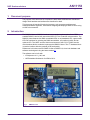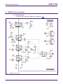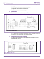
1
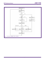
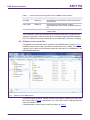
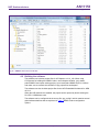
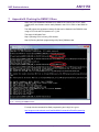
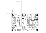
AN11153 DMX512/RDM slave using LPC111x Rev. 1 — 1 February 2012 Application note Document information Info Content Keywords LPC1110FD20; LPC1111FDH20; LPC1111FHN33; LPC1112FD20; LPC1112FDH20; LPC1112FDH28; LPC1112FHN33; LPC1112FHI33; LPC1113FHN33; LPC1113FBD48; LPC1114FDH28; LPC1114FN28; LPC1114FHN33; LPC1114FHI33; LPC1114FBD48; LPC1115FBD48; LPC111x, ARM, Cortex M0, DMX, DMX512, RDM, Architectural Lighting, Entertainment Lighting Abstract This application note describes the use of the NXP LPC111x Cortex M0 microcontroller to create an RDM enabled DMX512 Slave. AN11153 NXP Semiconductors DMX512/RDM slave using LPC111x Revision history Rev Date Description 1 Initial version. 20120201 Contact information For more information, please visit: http://www.nxp.com For sales office addresses, please send an email to: [email protected] AN11153 Application note All information provided in this document is subject to legal disclaimers. Rev. 1 — 1 February 2012 © NXP B.V. 2012. All rights reserved. 2 of 31 AN11153 NXP Semiconductors DMX512/RDM slave using LPC111x 1. Document purpose The purpose of this document is to explain the NXP DMX512/RDM slave demoboard design. Both hardware and software are described in detail. This document is intended for technical persons, such as system architects and hardware/software engineers, interested in designing/developing a DMX512 slave using an NXP microcontroller. 2. Introduction The DMX512 slave or DMX512 receiver is an example implementation for an RDM enabled DMX512 device built around the NXP LPC111x Cortex M0 microcontroller. The DMX512 slave features four DMX controllable LEDs, a red heartbeat LED, a green traffic LED, DIP switches for selecting the DMX start address, a 5-position joystick, and an optional LCD. The UART and the 16-bit timer/counters of the LPC111x MCU are the main hardware blocks needed to implement the DMX512 slave. The I2C hardware block is used to interface with the (optional) LCD functionality. References in this document to DMX512 refer to DMX512-A, since both hardware and software are designed using the latest standard[1]. The software can be built with • LPCXpresso v4.1.0_190, and • IAR Embedded Workbench for ARM v6.20.4. Fig 1. AN11153 Application note DMX512 slave All information provided in this document is subject to legal disclaimers. Rev. 1 — 1 February 2012 © NXP B.V. 2012. All rights reserved. 3 of 31 AN11153 NXP Semiconductors DMX512/RDM slave using LPC111x 3. DMX512 slave hardware 3.1 Physical layer The schematic of the physical DMX layer is depicted in Fig 2. Fig 2. DMX512 physical layer AN11153 Application note All information provided in this document is subject to legal disclaimers. Rev. 1 — 1 February 2012 © NXP B.V. 2012. All rights reserved. 4 of 31 AN11153 NXP Semiconductors DMX512/RDM slave using LPC111x The DMX bus connects to DATA+ and DATA- of DMX-IN and DMX-OUT. DMX-IN is a 5pole male XLR receptacle. DMX-OUT is a 5-pole female XLR receptacle. A 3-pin spare connector (not mounted) is available for other form factors. IC3 is an RS-485/RS422 transceiver, providing 15 kV ESD protection. The physical layer is electrically isolated from the DMX bus. The RX, TX and DIR signals from the microcontroller are optically isolated with high-speed optocouplers, and the supply for the optocouplers and bus transceiver are provided via the isolated DC/DC convertor (DC1). During startup the IO pins of the micro are high, and FET Q2 is used as an inverter to switch the DIR of IC3 to receive mode to avoid unwanted driving of the DMX bus. 3.2 Microcontroller The schematic of the microcontroller is depicted in Fig 3. Fig 3. Microcontroller on DMX512 slave The system is built around NXP’s new LPC1114 device, which is a Cortex-M0 running at frequencies of up to 50 MHz. Included are 32 kB on-chip flash, 8 kB SRAM, SSP, I2C, UART, ADC, etc. Debugging and flashing connection is provided by means of header SWD, which complies with the 10-pin SWD standard as supported by many flash and software tools. AN11153 Application note All information provided in this document is subject to legal disclaimers. Rev. 1 — 1 February 2012 © NXP B.V. 2012. All rights reserved. 5 of 31 AN11153 NXP Semiconductors DMX512/RDM slave using LPC111x The RESET button can be used to reset the microcontroller. A 4-channel DIP switch is added to support diversity. Two LEDs are provided, one red and one green. 3.3 User interface The schematic of the user interface is depicted in Fig 4. Fig 4. User interface on DMX512 slave The I2C alpha-numeric, 2x16 character LCD display is used to give feedback to the user. User commands can be entered with 5-way navigation switch S2. 3.4 LED interface and local LED feedback The DMX512 slave board delivers four PWM signals to an external light source (e.g., LED) on the LEDS_OUT plug. Fig 5. RGBW LED PWM output AN11153 Application note All information provided in this document is subject to legal disclaimers. Rev. 1 — 1 February 2012 © NXP B.V. 2012. All rights reserved. 6 of 31 AN11153 NXP Semiconductors DMX512/RDM slave using LPC111x The red, green, blue and white PWM signals are also connected to four corresponding on-board LEDs. The LEDs are placed in a circle, close to each other. When a diffuser is attached (not provided), the colors can be combined to form a single color. If the local feedback is not desired, it can be disabled with jumper LEDS_ENABLE. 3.5 Extension interface The DMX512 slave board also has an extension plug with system power, ground, I2C bus and RESET signal. Fig 6. I2C extension plug 3.6 System power The schematic of the power supply is depicted in Fig 7. Fig 7. AN11153 Application note Power circuit of DMX512 slave All information provided in this document is subject to legal disclaimers. Rev. 1 — 1 February 2012 © NXP B.V. 2012. All rights reserved. 7 of 31 AN11153 NXP Semiconductors DMX512/RDM slave using LPC111x A standard USB-mini-B plug is used to connect the 5 V system power. The ON LED illuminates when USB power is provided. Note: IC2 (SA57000-33D) is pin-compatible with the LP3985IM5-3.3 device. 3.7 Board layout The layout of the board (5.95” x 3.75”) is shown in Fig 8. Fig 8. Board layout of DMX512 slave On the left are the DMX-OUT and DMX-IN receptacles. On the top-left is the (not mounted) DMX extension plug. The left part of the board is electrically isolated from the right part on the division line through the middle of the optocouplers and the DC/DC convertor. The LCD display is at the top; below left are the two LEDs and below right is the navigation switch. In the circle are the four PWM-controlled LEDs, and to the right are the DIP switches and the microcontroller. At the bottom right are the RESET switch and the SWD interface. At the bottom are the USB power plug, the PWM LEDs outputs and the extension plug. AN11153 Application note All information provided in this document is subject to legal disclaimers. Rev. 1 — 1 February 2012 © NXP B.V. 2012. All rights reserved. 8 of 31 AN11153 NXP Semiconductors DMX512/RDM slave using LPC111x Table 1. Part DMX512 slave parts list Value Device Package Farnell Description RESET B3S1000 B3S1000 B3XS 177807 6.2 mm x 6.5 mm TACT Switch (SMD) Q2 BSH105 BSH105 SOT23 1758066 N-channel enhancement mode MOS transistor D11 BTHQ21605V-COGFSRE-I2C BTHQ21605VCOG-FSRE-I2C LCD_I2C 1220409 Batron I2C LCD Module, alphanumeric, 2X16 C10 100n C0805 P0805 Capacitor C13 100n C0805 P0805 Capacitor C14 100n C0805 P0805 Capacitor C15 100n C0805 P0805 Capacitor C19 100n C0805 P0805 Capacitor C20 100n C0805 P0805 Capacitor C21 100n C0805 P0805 Capacitor C24 100n C0805 P0805 Capacitor C25 100n C0805 P0805 Capacitor C5 100n C0805 P0805 Capacitor C9 100n C0805 P0805 Capacitor C17 180n C0805 P0805 Capacitor C16 1u C0805 P0805 Capacitor C18 1u C0805 P0805 Capacitor C22 220n C0805 P0805 Capacitor C23 220n C0805 P0805 Capacitor C7 220n C0805 P0805 Capacitor C3 22p C0805 P0805 Capacitor C4 22p C0805 P0805 Capacitor C6 2u2 C0805 P0805 Capacitor C8 2u2 C0805 P0805 Capacitor C1 4u7 C0805 P0805 Capacitor C11 4u7 C0805 P0805 Capacitor C12 4u7 C0805 P0805 Capacitor C2 4u7 C0805 P0805 Capacitor Q1 AKER-C3E-12MHz CRYSTAL4 XTAL4 1640974 Crystal, 2.5 mm x 3 mm DIR FOD060L FOD060L SOIC08 1228309 Fairchild Opto Coupler, 3V3, high-speed, 10 Mbit/s RX FOD060L FOD060L SOIC08 1228309 Fairchild Opto Coupler, 3V3, high-speed, 10 Mbit/s TX FOD060L FOD060L SOIC08 1228309 Fairchild Opto Coupler, 3V3, high-speed, 10 Mbit/s SWD FTSH-105-DV FTSH-105-DV 127_2R10_SMT 1767036 Samtec connector, 10way AN11153 Application note All information provided in this document is subject to legal disclaimers. Rev. 1 — 1 February 2012 © NXP B.V. 2012. All rights reserved. 9 of 31 AN11153 NXP Semiconductors DMX512/RDM slave using LPC111x Part Device Package LEDS_ENABLE JP1E JP1E JP1 JUMPER L1 BLM18AG601S L0603 P0603 Inductor L2 BLM18AG601S L0603 P0603 Inductor L3 BLM18AG601S L0603 P0603 Inductor IC1 LPC1114FBD48/301 LPC1113/14LQFP48 LQFP48 1786289 NXP Semiconductors, Cortex-M0 MCU, 32-bit L4 10uH L-USL1812 L1812 1174073 INDUCTOR, American symbol S1 MCDHN-4F-T-V MCDHN-4F-T-V DIP4 1605479 DIP Switch SMD, 4-way DMX-OUT NC5FAH NC5FAH NC5FAH 8020418 Neutrik Audio Connector XLR SERIES DMX-IN NC5MAH NC5MAH NC5MAH 8020396 Neutrik Audio Connector XLR SERIES DC1 NKE0303SC NME NME 1175765 DC-DC CONVERTER W OVS-0801 (W) OVS-0801(W) CHIPLED_0805 1716764 Chip LED 0805 B OVS-0803 (B) OVS-0803(B) CHIPLED_0805 1716765 Chip LED 0805 ON OVS-0803 (B) OVS-0803(B) CHIPLED_0805 1716765 Chip LED 0805 G OVS-0804 (G) OVS-0804(G) CHIPLED_0805 1716766 Chip LED 0805 LED2 OVS-0804 (G) OVS-0804(G) CHIPLED_0805 1716766 Chip LED 0805 LED1 OVS-0808 (R) OVS-0808(R) CHIPLED_0805 1716768 Chip LED 0805 R OVS-0808 (R) OVS-0808(R) CHIPLED_0805 1716768 Chip LED 0805 EXT nc PINHD-1X5 1X05 PIN HEADER LEDS_OUT nc PINHD-1X6 1X06 PIN HEADER R22 100E R0805 P0805 Resistor R15 10k R0805 P0805 Resistor R16 10k R0805 P0805 Resistor R17 10k R0805 P0805 Resistor R18 10k R0805 P0805 Resistor R20 10k R0805 P0805 Resistor R21 10k R0805 P0805 Resistor R5 10k R0805 P0805 Resistor R6 10k R0805 P0805 Resistor R8 150E R0805 P0805 Resistor R1 1k R0805 P0805 Resistor R2 1k R0805 P0805 Resistor R35 1k5 R0805 P0805 Resistor R10 390E R0805 P0805 Resistor R14 390E R0805 P0805 Resistor R7 390E R0805 P0805 Resistor R9 390E R0805 P0805 Resistor R11 3k3 R0805 P0805 Resistor R12 3k3 R0805 P0805 Resistor AN11153 Application note Value Farnell All information provided in this document is subject to legal disclaimers. Rev. 1 — 1 February 2012 Description © NXP B.V. 2012. All rights reserved. 10 of 31 AN11153 NXP Semiconductors DMX512/RDM slave using LPC111x Part Value Device Package R13 3k3 R0805 P0805 Resistor R23 3k3 R0805 P0805 Resistor R19 47k R0805 P0805 Resistor R3 560E R0805 P0805 Resistor R4 560E R0805 P0805 Resistor IC2 SA57000-33D SA57000-33D SOT23-5 1826832 CapFREE 150 mA, lownoise, low-drop regulator S2 SKQUDBE010 SKQUDBE010 JOYSTICK 1435776 Joystick, 4-directions with center push, SKQU IC3 SP3075EEN-L SP3075EEN-L SO08 9386688 RS-485/RS422 transceivers TP1 TPSPAD1-13 TPSPAD1-13 P1-13 TEST PIN TP2 TPSPAD1-13 TPSPAD1-13 P1-13 TEST PIN X5 USB-MB-SMD USB-MB-SMD USB-MB-SMD DMX nc W237-103 W237-103 AN11153 Application note Farnell 1654060 All information provided in this document is subject to legal disclaimers. Rev. 1 — 1 February 2012 Description MINI USB-B connector WAGO SCREW CLAMP © NXP B.V. 2012. All rights reserved. 11 of 31 AN11153 NXP Semiconductors DMX512/RDM slave using LPC111x 4. DMX512 slave software This section first describes the software architecture and the main software execution flow. The second part of this section explains the software structure in more detail. 4.1 Architecture The software of the DMX512 slave has a modular architecture, meaning that each hardware block has its own software driver. To keep the memory footprint of the firmware as small as possible, the software running on the DMX512 slave does not incorporate a Real Time Operating System. The software is written in the “C” programming language. Functionality can be easily enabled or disabled before building the software, such as support of the local LCD and support of RDM (see Section 4.9), in order to get a smaller flash memory footprint. When RDM support is enabled, bidirectional communication will be used between the DMX512 master and the DMX512 slave. Fig 9 shows the architectural block diagram. Fig 9. Software architecture of DMX512 slave 4.2 Main software execution flow Fig 10 shows the flowchart of the DMX512 slave software. The DMX slave init is described in Section 4.4. The following described actions are repeated until the DMX512 slave is powered down or reset. The main loop starts with reading a DMX512 packet from the DMX transmission line. This is done by calling the function Uart_RecvDmxSlotValues(). This read action times out after one second, being the maximum time between two successive DMX512 packets, when no data is received. This timeout could be caused by the DMX512 master being powered down or disconnected from the DMX transmission line, the DMX512 slave being disconnected from the DMX transmission line, the transmission line being broken, or a hardware conflict on the DMX transmission line. AN11153 Application note All information provided in this document is subject to legal disclaimers. Rev. 1 — 1 February 2012 © NXP B.V. 2012. All rights reserved. 12 of 31 AN11153 NXP Semiconductors DMX512/RDM slave using LPC111x When a timeout occurs the four DMX controlled LEDs are turned OFF, and the text “No packets from DMX512 master” is shown on the LCD. This text is removed from the LCD as soon as a DMX512 NULL START packet is received. When the read action is successful the GREEN traffic LED is toggled. The traffic LED is an indication of how many DMX512 packets are received per second: slow blinking means low traffic; fast blinking means high traffic; no blinking means no traffic or the receiving circuit of DMX512 slave is broken. Then the DMX512 start code (also called slot 0, or the first byte of the packet) is checked to be a NULL START code (hexadecimal 0x00), the Alternate START code 23 (hexadecimal 0x17) indicating an ASCII Text packet, or the START code 204 (hexadecimal 0xCC) indicating a RDM packet. The received slot data from the NULL START code packet is used to drive the four DMX controllable LEDs (dimmable from 0 % to 100 %). When no new data is received for one or more of the DMX controlled LEDs, because the DMX transmission didn’t include these slots, these LEDs are turned OFF. When none of the four DMX controllable LEDs is addressed with a NULL START code packet, the text “Not addressed by DMX512 master” is shown on the LCD. If the example software is built without RDM support, the position of the DIP switches is read again, to determine which DMX slots (channels) the DMX512 slave will listen to; the DMX512 slave does not need a power down/up or reset to let it listen to other DMX slots. When an ASCII text packet is received, the first 32 characters of this message are displayed on the LCD. When an RDM packet is received, it will only be handled when it is addressed to this DMX512 slave, or when it is a broadcast message (see Section 4.3 for more details). The last action in the main loop is triggering the WatchDog Timer (WDT). If the WDT isn’t triggered for six seconds (this should never happen because of the one second read timeout), the DMX512 slave will be reset, resulting in the start message being shown on the LCD. AN11153 Application note All information provided in this document is subject to legal disclaimers. Rev. 1 — 1 February 2012 © NXP B.V. 2012. All rights reserved. 13 of 31 AN11153 NXP Semiconductors DMX512/RDM slave using LPC111x Fig 10. Flowchart of DMX512 slave software AN11153 Application note All information provided in this document is subject to legal disclaimers. Rev. 1 — 1 February 2012 © NXP B.V. 2012. All rights reserved. 14 of 31 AN11153 NXP Semiconductors DMX512/RDM slave using LPC111x 4.3 RDM The Remote Device Management (RDM) protocol[3] permits intelligent bidirectional communication between a DMX512 master and a DMX512 slave. RDM enables DMX device discovery (when connected to the DMX transmission line) plus management and control of the DMX device. Examples of RDM messages (control packets) are: change (set) DMX start address, get DMX device state info (e.g., lamp burning hours, power cycles, etc), RDM device self test, etc. This DMX512 slave illustrates the mandatory RDM messages. Extension of the supported RDM messages is very easy with our example software implementation. RDM has only six command classes (see Table 2) in which the RDM packets can be grouped. Table 2. RDM command class defines RDM command classes Value DISCOVERY_COMMAND 0x10 DISCOVERY_COMMAND_RESPONSE 0x11 GET_COMMAND 0x20 GET_COMMAND_RESPONSE 0x21 SET_COMMAND 0x30 SET_COMMAND_RESPONSE 0x31 Table 3 shows the implemented RDM packets and the command class to which they belong. Table 3. Implemented RDM packets Discovery class Get class Set class RDM PID Value ● DISC_UNIQUE_BRANCH 0x0001 ● DISC_MUTE 0x0002 ● DISC_UN_MUTE 0x0003 ● DEVICE_INFO 0x0060 ● SOFTWARE_VERSION_LABEL 0x00C0 ● ● DMX_START_ADDRESS 0x00F0 ● ● IDENTIFY_DEVICE 0x1000 Each RDM device has a 48-bit unique device ID or UID; the most significant 16-bits are reserved for the manufacturer ID. Example software described in this manual uses the NXP RDM manufacturer ID hexadecimal 0x3B10, given by the following formula: #define MAN_ID ((32*32*('N'-'@')) + (32*('X'-'@')) + ('P'-'@')) Any NXP customer that wants to create an RDM enabled DMX device should apply for (and use) its own manufacturer ID at PLASA[4]. AN11153 Application note All information provided in this document is subject to legal disclaimers. Rev. 1 — 1 February 2012 © NXP B.V. 2012. All rights reserved. 15 of 31 AN11153 NXP Semiconductors DMX512/RDM slave using LPC111x 4.3.1 Device discovery For the DMX512 master to be able to send RDM packets to specific RDM devices, the DMX512 master must first discover the UIDs of the RDM devices connected to the DMX transmission line. This is done by the discovery process, driven by the DMX512 master or a host (PC) that controls the DMX512 master. This discovery process makes use of a binary search mechanism to search over the total 48-bit address range. An RDM device should only handle an RDM packet when this packet is addressed to this RDM device (its own UID), or when it is a broadcast message. The RDM device shall only send a response packet to the DMX512 master when the RDM packet was addressed to its own UID, or when its UID was in the lower bound and upper bound UID range of the DISC_UNIQUE_BRANCH RDM packet. Responding on the DISC_UNIQUE_BRANCH RDM packet is the only time that collisions might take place on the DMX transmission line. When an RDM device is uniquely identified during the discovery process, it is muted by sending a DISC_MUTE RDM packet to this RDM device; this keeps it from interfering with the discovery process (sending back responses to the DMX512 master) when the search for other RDM devices is continued. For a full discovery, the discovery process will start by un-muting all RDM devices by sending a DISC_UN_MUTE RDM broadcast message. An RDM broadcast message is identified by the 48-bit destination UID having the hexadecimal value 0xFFFFFFFFFFFF. After the discovery process has finished, the DMX512 master can get the device info, software version label, DMX start address, and identify state of the DMX512 slave. Furthermore, the DMX512 master can assign another DMX start address to the DMX512 slave, and it can ask the slave to identify itself. The new DMX start address is not permanently stored in some NVM, meaning that after a power cycle or reset the DMX512 slave will have its default DMX address as defined by the setting of the DIP switches. When the DMX512 slave receives the RDM packet IDENTIFY_DEVICE with parameter IDENTIFY_ON, it will turn ON the four DMX controllable LEDs (100 %) and the text “You found me ” is shown on the LCD. After receiving the RDM packet IDENTIFY_DEVICE with parameter IDENTIFY_OFF, the four DMX controllable LEDs will be turned OFF, and the LCD is cleared. Disconnecting the DMX512 slave from the DMX transmission line while its identify state is IDENTIFY_ON will NOT turn OFF the four LEDs and the identify text is NOT removed from the LCD. For more info on Remote Device Management see Reference [3]. 4.4 Initialization sequence When the LPC111x microcontroller starts up (as a result of the DMX512 slave being powered), the stack pointer is loaded with the value from address 0:3, and the program counter is loaded with the value from address 4:7 (the address of the reset handler). This will result in the calling of main(). The function main() implements an infinite loop which receives data from the DMX transmission line, drives the LEDs, and the (optional) LCD. Before the infinite loop is entered the function SystemInit() is called, which sets up the main PLL that is used to set the proper CPU clock, as configured by LPC_CORE_CLOCKSPEED_HZ in ‘app_config.h’. Function SystemInit() comes with CMSIS. After calling SystemInit() the function bsp_init() is called. This function sets up the system tick counter to 1000 ticks per second; it enables the HW blocks GPIO / I2C / CT16B0 / CT16B1 / CT32B0 / UART / WDT; it configures the LPC pins for controlling the LEDs / dip switches / UART pins / I2C pins / etc.; and it initializes the PWM counter_timer driver, DMX UART driver, I2C driver, LCD driver and WDT driver. Then init_globals() is AN11153 Application note All information provided in this document is subject to legal disclaimers. Rev. 1 — 1 February 2012 © NXP B.V. 2012. All rights reserved. 16 of 31 AN11153 NXP Semiconductors DMX512/RDM slave using LPC111x called which reads out the DIP switches and determines the DMX start address of the DMX512 slave. The four DIP switches are used to select 1 of 16 DMX slot ranges. Each range covers (512 / 16 =) 32 slots; the last four slots are used to address the four DMX controllable LEDs. Table 4. Dip switch translation into DMX512 slave address Dip switch setting DMX512 slave address (and slot usage) 0 DMX slave address = 29 This means: Slot[29] = Red LED Slot[30] = Green LED Slot[31] = Blue LED Slot[32] = White LED x DMX slave address = (x * 32) + 29 This means: Slot[(x*32)+29] = Red LED Slot[(x*32)+30] = Green LED Slot[(x*32)+31] = Blue LED Slot[(x*32)+32] = White LED 15 DMX slave address = 509 This means: Slot[509] = Red LED Slot[510] = Green LED Slot[511] = Blue LED Slot[512] = White LED When built with RDM support, this DMX address can be changed via RDM. After calling init_globals() the DMX controlled LEDs are switched ON so that the user can check that they are working; in addition, the text “NXP LPC1114 DMX512 slave” is shown on the LCD. After this the main loop is entered. 4.5 DMX UART driver The UART driver is specially written for receiving/transmitting DMX/RDM packets from/to the DMX transmission line. A DMX packet always starts with a “Break” (the only exception being the response on a DISC_UNIQUE_BRANCH packet), TX line being low for at least 92 micro seconds, followed by a “Mark”, TX line being high for at least 12 micro seconds. See Reference [1] for more detailed information on DMX timing. This sequence indicates the start of the DMX packet. The bytes following the synchronization header have the structure of one start bit, eight data bits, no parity bits, and two stop bits, making it a total of 11 bits per data byte. The first byte is the start byte (or slot 0) and is followed by up to 512 bytes (slot 1 up till slot 512). The slots are also referred to as channels, so a maximum of 512 channels can be driven by the DMX packet (slot 0 is used for the type of packet indication). Slot 1 is channel 1, slot 2 is channel 2, up to 512. The transmission speed is fixed at 250 kbit/s (+/- 2 %). The UART driver is initialized by the BSP. Since the communication settings (baud rate, parity, etc) are fixed for DMX, the function Uart_Init() does not have parameters for this in its arguments list. Function Uart_Init() takes care for initializing the variables used within the UART driver, initializes the UART hardware block, claims a milliseconds counter (to be used for timeout purposes) via the BSP, and enables the UART receive data IRQ. The UART driver uses double buffering (two internal byte arrays of 513 bytes each) for AN11153 Application note All information provided in this document is subject to legal disclaimers. Rev. 1 — 1 February 2012 © NXP B.V. 2012. All rights reserved. 17 of 31 AN11153 NXP Semiconductors DMX512/RDM slave using LPC111x receiving slot 0 up till slot 512 from the DMX transmission line. When one buffer is filled with received slot values, a pointer to this buffer is passed back to the DMX512 slave application while continuing to receive and store new slot values in the other buffer. The next time a buffer is full, a pointer to this buffer is passed back to the DMX512 slave application, preventing any unnecessary data copies. The received slot values are stored in the buffers by the UART interrupt handler. In the case of a NULL START packet the application can select the channels from these buffers in which it is interested (depending on its DMX address), for dimming the LEDs. In the case of an ASCII text packet, the buffer holds the complete text packet (maximum 510 characters including the terminating zero). In the case of an RDM packet, the buffer holds the complete RDM packet. 4.6 PWM counter/timer driver The DMX512 slave uses two 16-bit counter/timers to drive the four RGBW LEDs; each counter/timer drives two LEDs using three of the four available match registers per CT to create a Pulse Width Modulation signal to steer the LEDs. For CT16B0, the output of match register 0 is used for driving the RED LED (PWM mode); the output of match register 1 is used for driving the GREEN LED (PWM mode); and match register 3 is used for setting the frequency for the RED and GREEN LEDs. For CT16B1, the output of match register 0 is used for driving the BLUE LED (PWM mode); the output of match register 1 is used for driving the WHITE LED (PWM mode); and match register 3 is used for setting the frequency for the BLUE and WHITE LEDs. The PWM frequency of all four LEDs is taken from the same define PWM_FREQ with a value of 733 Hz. The counter/timer driver exports three functions; only two are used in the DMX512 slave software. The BSP calls the function Timer_PWM_Init() for the hardware blocks CT16B0 and CT16B1. This initialization function programs the registers of the requested counter/timer and sets an initial pulse width duty cycle of 50 %. The second function used in this counter/timer driver is Timer_PWM_Set_Duty_Cycle(), which is called from the main loop when a NULL START packet is received. A linear transformation is used from slot value into duty cycle, so a slot value of 0 corresponds with a duty cycle of 0 %, a slot value of 5 corresponds with a duty cycle of 2 %, and a slot value of 250 up to 255 corresponds with a duty cycle of 100 %. 4.7 Interrupts The LPC111x microcontroller has four interrupt priority levels, where 0 is the highest and 3 the lowest priority level. Table 5 shows the interrupts that are handled by the software, the interrupt priority of each interrupt, and between brackets the actual interrupt priority level. AN11153 Application note All information provided in this document is subject to legal disclaimers. Rev. 1 — 1 February 2012 © NXP B.V. 2012. All rights reserved. 18 of 31 AN11153 NXP Semiconductors DMX512/RDM slave using LPC111x Table 5. Interrupt Used interrupts and assigned priorities in DMX512 slave software Priority Description I2C_IRQn Highest (1) Generated by the I2C HW block. Used for writing text to the LCD panel. UART_IRQn Middle (2) Generated by the UART HW block. Used for transmitting/receiving data to/from the DMX transmission line. TickHandler Lowest (3) Generated by the systick timer. Used for implementing software timers. The TickHandler is called every millisecond to increment millisecond counters that are used by the application. After each second the TickHandler toggles the RED heartbeat LED. The millisecond counters overflow after 2^32 milliseconds (1193 hours = 49 days). 4.8 Software source code files The software tree holding the source code files of the DMX512 slave is shown in Fig 11. All DMX512 slave source code is contained in the directory LPC111xSlave. The files “.cproject” and “.project” are LPCXpresso project files; the files LPC111xDMXslave.*” are IAR EWARM project files. Fig 11. Software tree of DMX512 slave This directory also contains a “CMSIS” directory containing the CMSIS source code, and all the source files of Fig 12 in the directory “src”, which is the source code that forms the heart of the DMX512 slave. A brief description of these source code files is shown in Table 6. AN11153 Application note All information provided in this document is subject to legal disclaimers. Rev. 1 — 1 February 2012 © NXP B.V. 2012. All rights reserved. 19 of 31 AN11153 NXP Semiconductors DMX512/RDM slave using LPC111x Table 6. Source code file description File name Description app_config.h Configures the DMX512 slave application bsp.c This file implements the “board support package”, software functions specific for this MCU and the electronics (LEDs/switches/etc) on the PCB bsp.h Header file describing the exported functions by bsp.c cr_startup_lpc111x.c This file contains the Reset vector and exception vector table (needed for the LPCXpresso build only) AN11153 Application note i2c.c Software driver for the I2C hardware block i2c.h Header file describing the exported functions by i2c.c lcd.c Software driver for the LCD mounted on the DMX512 slave PCB lcd.h Header file describing the exported functions by lcd.c main.c This file contains the application entry point, main loop and RDM packet handling main.h Header file describing the exported functions by main.c manual_ctrl.c Implements joystick support for stand-alone RGB controller functionality manual_ctrl.h Header file describing the exported functions by manual_ctrl.h startup_armcm0.s Assembly file containing the Reset vector and exception vector table (needed for the IAR build only) timer_pwm.c SW driver for the counter/timer hardware blocks, using PWM to dim the RGB LEDs timer_pwm.h Header file describing the exported functions by timer_pwm.c uart.c Software driver for the UART hardware block especially for DMX512 packet RTX uart.h Header file describing the exported functions by uart.c wdt.c Software driver for the WDT hardware block wdt.h Header file describing the exported functions by wdt.c All information provided in this document is subject to legal disclaimers. Rev. 1 — 1 February 2012 © NXP B.V. 2012. All rights reserved. 20 of 31 AN11153 NXP Semiconductors DMX512/RDM slave using LPC111x Fig 12. DMX512 slave source code files 4.9 Building the software The software tree includes project files for LPCXpresso v4.1.0_190. When using LPCXpresso for building the DMX512 slave, use workspace location <your install path>\DMX512 and import existing project <your install path>\DMX512\LPC111xSlave and make sure to uncheck the checkbox "Copy projects into workspace". The software tree also includes project files for the IAR Embedded Workbench for ARM v6.20.4. When the IAR workbench is installed, the project can be opened by double clicking the file ‘LPC111xDMXslave.eww’. The software can be configured via the source file ‘app_config.h’ which contains several global software defines that are explained in Table 7 DMX512 slave configuration options. AN11153 Application note All information provided in this document is subject to legal disclaimers. Rev. 1 — 1 February 2012 © NXP B.V. 2012. All rights reserved. 21 of 31 AN11153 NXP Semiconductors DMX512/RDM slave using LPC111x Table 7. Define DMX512 slave configuration options Description LPC_CORE_CLOCKSPEED_HZ Sets the CPU clock. SUPPORT_RDM_OVER_DMX512 Must be enabled when the DMX512 slave must support Remote Device Management SUPPORT_I2C_BUS Must be enabled when text output on the LCD is required. SUPPORT_I2C_MASTER_MODE Must be enabled when text output on the LCD is required. The LPC111x is I2C master, the LCD is I2C slave. SUPPORT_MANUAL_CONTROL Must be enabled when software support for the joystick is wanted. This software shows how to use the DMX512 slave as a stand-alone RGB controller. By default the CPU clock is configured at 48 MHz, being a multiple of 12 MHz. A DEBUG build doesn’t optimize the executable image, which makes it possible to debug the software. A RELEASE build is optimized for size, which reduces the flash memory footprint significantly. Table 8 shows the firmware sizes (in bytes) of a RELEASE build of the DMX512 slave for a DMX512 only build, a DMX512 build with RDM support, and a full featured build. Table 8. DMX512 slave firmware sizes Firmware sizes IAR EWARM v6.20.4 for DMX512 Flash [Bytes] RAM [Bytes] slave (Release build) LPCXpresso v4.1.0_190 Flash [Bytes] RAM [Bytes] DMX512 3344 + 48 1435 3988 12 + 1108 DMX512+RDM 4876 + 48 1529 5668 12 + 1196 DMX512+RDM+ joystick 7800 + 164 1617 9208 48 + 1248 4.10 Summary It has been tested/verified that the firmware currently implemented on the DMX512 slave (as described in the previous paragraphs) also runs on 12 MHz, and that even at this CPU speed it can handle the maximum DMX512 bus load (512+1 slots at 44 Hz). This means that there are still enough CPU cycles available to add extra functionality to the DMX512 slave. AN11153 Application note All information provided in this document is subject to legal disclaimers. Rev. 1 — 1 February 2012 © NXP B.V. 2012. All rights reserved. 22 of 31 AN11153 NXP Semiconductors DMX512/RDM slave using LPC111x 5. Document management 5.1 Abbreviations Table 9. Abbreviations Acronym Description AN11153 Application note BSP Board Support Package CMSIS Cortex Microcontroller Software Interface Standard CPU Central Processing Unit CT Counter Timer GPIO General Purpose Input/Output HW Hardware IRQ Interrupt Request I2C Inter Integrated Circuit LCD Liquid Crystal Display LED Light Emitting Diode MCU Micro Controller Unit NVM Non Volatile Memory PC Personal Computer PCB Printed Circuit Board PLASA The lead international membership body for those who supply technologies and services to the event, entertainment and installation industries PLL Phase Locked Loop PWM Pulse Width Modulation RDM Remote Device Management RGB Red Green Blue RTX Receive and Transmit SW Software UART Universal Asynchronous Receiver/Transmitter UID Unique device ID WDT Watchdog Timer All information provided in this document is subject to legal disclaimers. Rev. 1 — 1 February 2012 © NXP B.V. 2012. All rights reserved. 23 of 31 AN11153 NXP Semiconductors DMX512/RDM slave using LPC111x 5.2 Referenced documents Table 10. Referenced documents Doc Title [1] ANSI E1.11 - Asynchronous Serial Data Transmission Standard for Controlling Lighting Equipment and Accessories [2] UM10398 - LPC111x/LPC11Cxx User manual [3] ANSI E1.20 - Remote Device Management Over DMX512 Networks [4] PLASA manufacturer ID’s http://tsp.plasa.org/tsp/working_groups/CP/mfctrIDs.php AN11153 Application note All information provided in this document is subject to legal disclaimers. Rev. 1 — 1 February 2012 Version Author Issue Date 2008 ESTA 20081204 Rev. 4 NXP 20110304 2010 PLASA 20110104 © NXP B.V. 2012. All rights reserved. 24 of 31 AN11153 NXP Semiconductors DMX512/RDM slave using LPC111x 6. Appendix A: Testing the DMX512 slave 6.1 USB power Action Power the DMX512 slave (disconnected from DMX512 bus) via the USB connector X5. Result The BLUE ON LED (just above the USB connector) must light up continuously. The LPC1114 must start to run the firmware resulting in: • Turning on GREEN LED2. • For one second the LEDS R (RED), G (GREEN), B (BLUE), W (WHITE) will light up (only when the LEDS ENABLE jumper is placed) and the LCD must display the text “NXP LPC1114 DMX512 slave”. • After one second the LCD must display the text “No packets from DMX512 master” and the RED LED1 starts to blink with a 1 Hz frequency 6.2 DMX512 input Action Connect DMX512 slave to DMX512 bus which carries 512 slots of data. Result The GREEN LED2 blinks with the refresh rate of the DMX512 packets on the bus. The LEDS R (RED), G (GREEN), B (BLUE), W (WHITE) will light up depending on the received data values of the slots assigned to these LEDS (DMX start address). The LCD is blank. 6.3 DMX512 output Action Connect DMX512 slave to DMX512 bus and do an RDM discovery. Result Each DMX512 slave should be discovered via bi-directional RDM packets. 6.4 Reset button Action Press the reset button while the board is powered (and keep it pressed). Result The BLUE ON LED (just above the USB connector) stays on. The RED LED1 stops blinking and doesn’t light up. The GREEN LED2 turns off. Any text on the LCD keeps being displayed. Action Release the reset button. Result The LPC1114 must start to run the firmware resulting in the GREEN LED2 to turn on. For one second the LEDS R (RED), G (GREEN), B (BLUE), W (WHITE) will light up (only when the LEDS ENABLE jumper is placed) and the LCD must display the text “NXP LPC1114 DMX512 slave”. After one second the LCD must display the text “No packets from DMX512 master” and the RED LED1 starts to blink with a 1 Hz frequency. AN11153 Application note All information provided in this document is subject to legal disclaimers. Rev. 1 — 1 February 2012 © NXP B.V. 2012. All rights reserved. 25 of 31 AN11153 NXP Semiconductors DMX512/RDM slave using LPC111x 6.5 Joystick Action Press the joystick (center switch) while the board is powered, and keep it pressed for 1 second. Result The LCD must display the text: MANUAL CONTROL 1 Go The RED LED1 keeps blinking with a 1 Hz frequency AN11153 Application note Action Use the UP / DOWN / LEFT / RIGHT / center switches of the joystick while the board is powered and while in MANUAL CONTROL (see previous action). Result With the joystick the user can navigate through the following menu (visible on the LCD display): MANUAL CONTROL 1 Go 2 Set colors 3 Version info 4 Quit 1.1 Mode 1.2 Speed 1.3 Dim 1.4 Quit 1 10 100 2.1 Color 2.2 Hue 2.3 Sat 2.4 Bright 2.5 Quit 1 0 100 100 All information provided in this document is subject to legal disclaimers. Rev. 1 — 1 February 2012 © NXP B.V. 2012. All rights reserved. 26 of 31 AN11153 NXP Semiconductors DMX512/RDM slave using LPC111x 7. Appendix B: Flashing the DMX512 Slave When using IAR Embedded Workbench for ARM v6.20.4 and a j-link JTAG / SWD +SWO probe, the firmware can be easily flashed in the LPC1114/301 of the DMX512 slave. The IAR project also generates a binary file that can be flashed in the DMX512 slave using a LPC-Link and LPCXpresso v4.1.0_190. The steps for Windows7 are: Step 1) Booting LPC-Link ‘boot_LPC-link.bat’ Step 2) Running the flash programming utility ‘flash_DMXslave.bat’ Fig 13. Flashing the DMX512 slave For help with the command line flash programming tool using Linux, go to: http://support.code-red-tech.com/CodeRedWiki/CommandLineFlashProgramming AN11153 Application note All information provided in this document is subject to legal disclaimers. Rev. 1 — 1 February 2012 © NXP B.V. 2012. All rights reserved. 27 of 31 AN11153 NXP Semiconductors DMX512/RDM slave using LPC111x 8. Legal information 8.1 Definitions Draft — The document is a draft version only. The content is still under internal review and subject to formal approval, which may result in modifications or additions. NXP Semiconductors does not give any representations or warranties as to the accuracy or completeness of information included herein and shall have no liability for the consequences of use of such information. 8.2 Disclaimers Limited warranty and liability — Information in this document is believed to be accurate and reliable. However, NXP Semiconductors does not give any representations or warranties, expressed or implied, as to the accuracy or completeness of such information and shall have no liability for the consequences of use of such information. NXP Semiconductors takes no responsibility for the content in this document if provided by an information source outside of NXP Semiconductors. In no event shall NXP Semiconductors be liable for any indirect, incidental, punitive, special or consequential damages (including - without limitation lost profits, lost savings, business interruption, costs related to the removal or replacement of any products or rework charges) whether or not such damages are based on tort (including negligence), warranty, breach of contract or any other legal theory. Notwithstanding any damages that customer might incur for any reason whatsoever, NXP Semiconductors’ aggregate and cumulative liability towards customer for the products described herein shall be limited in accordance with the Terms and conditions of commercial sale of NXP Semiconductors. Right to make changes — NXP Semiconductors reserves the right to make changes to information published in this document, including without limitation specifications and product descriptions, at any time and without notice. This document supersedes and replaces all information supplied prior to the publication hereof. Suitability for use — NXP Semiconductors products are not designed, authorized or warranted to be suitable for use in life support, life-critical or safety-critical systems or equipment, nor in applications where failure or malfunction of an NXP Semiconductors product can reasonably be expected to result in personal injury, death or severe property or environmental damage. NXP Semiconductors and its suppliers accept no liability for inclusion and/or use of NXP Semiconductors products in such equipment or applications and therefore such inclusion and/or use is at the customer’s own risk. Applications — Applications that are described herein for any of these products are for illustrative purposes only. NXP Semiconductors makes no representation or warranty that such applications will be suitable for the specified use without further testing or modification. Semiconductors accepts no liability for any assistance with applications or customer product design. It is customer’s sole responsibility to determine whether the NXP Semiconductors product is suitable and fit for the customer’s applications and products planned, as well as for the planned application and use of customer’s third party customer(s). Customers should provide appropriate design and operating safeguards to minimize the risks associated with their applications and products. NXP Semiconductors does not accept any liability related to any default, damage, costs or problem which is based on any weakness or default in the customer’s applications or products, or the application or use by customer’s third party customer(s). Customer is responsible for doing all necessary testing for the customer’s applications and products using NXP Semiconductors products in order to avoid a default of the applications and the products or of the application or use by customer’s third party customer(s). NXP does not accept any liability in this respect. Export control — This document as well as the item(s) described herein may be subject to export control regulations. Export might require a prior authorization from competent authorities. Evaluation products — This product is provided on an “as is” and “with all faults” basis for evaluation purposes only. NXP Semiconductors, its affiliates and their suppliers expressly disclaim all warranties, whether express, implied or statutory, including but not limited to the implied warranties of noninfringement, merchantability and fitness for a particular purpose. The entire risk as to the quality, or arising out of the use or performance, of this product remains with customer. In no event shall NXP Semiconductors, its affiliates or their suppliers be liable to customer for any special, indirect, consequential, punitive or incidental damages (including without limitation damages for loss of business, business interruption, loss of use, loss of data or information, and the like) arising out the use of or inability to use the product, whether or not based on tort (including negligence), strict liability, breach of contract, breach of warranty or any other theory, even if advised of the possibility of such damages. Notwithstanding any damages that customer might incur for any reason whatsoever (including without limitation, all damages referenced above and all direct or general damages), the entire liability of NXP Semiconductors, its affiliates and their suppliers and customer’s exclusive remedy for all of the foregoing shall be limited to actual damages incurred by customer based on reasonable reliance up to the greater of the amount actually paid by customer for the product or five dollars (US$5.00). The foregoing limitations, exclusions and disclaimers shall apply to the maximum extent permitted by applicable law, even if any remedy fails of its essential purpose. 8.3 Trademarks Notice: All referenced brands, product names, service names and trademarks are property of their respective owners. Customers are responsible for the design and operation of their applications and products using NXP Semiconductors products, and NXP AN11153 Application note All information provided in this document is subject to legal disclaimers. Rev. 1 — 1 February 2012 © NXP B.V. 2012. All rights reserved. 28 of 31 AN11153 NXP Semiconductors DMX512/RDM slave using LPC111x 9. List of figures Fig 1. Fig 2. Fig 3. Fig 4. Fig 5. Fig 6. Fig 7. Fig 8. Fig 9. Fig 10. Fig 11. Fig 12. Fig 13. DMX512 slave ................................................... 3 DMX512 physical layer ..................................... 4 Microcontroller on DMX512 slave ..................... 5 User interface on DMX512 slave ...................... 6 RGBW LED PWM output .................................. 6 I2C extension plug ............................................. 7 Power circuit of DMX512 slave ......................... 7 Board layout of DMX512 slave.......................... 8 Software architecture of DMX512 slave .......... 12 Flowchart of DMX512 slave software .............. 14 Software tree of DMX512 slave ...................... 19 DMX512 slave source code files ..................... 21 Flashing the DMX512 slave ............................ 27 AN11153 Application note All information provided in this document is subject to legal disclaimers. Rev. 1 — 1 February 2012 © NXP B.V. 2012. All rights reserved. 29 of 31 AN11153 NXP Semiconductors DMX512/RDM slave using LPC111x 10. List of tables Table 1. Table 2. Table 3. Table 4. DMX512 slave parts list .................................... 9 RDM command class defines ......................... 15 Implemented RDM packets ............................. 15 Dip switch translation into DMX512 slave address ........................................................... 17 Table 5. Used interrupts and assigned priorities in DMX512 slave software .................................. 19 Table 6. Source code file description ............................ 20 Table 7. DMX512 slave configuration options ............... 22 Table 8. DMX512 slave firmware sizes ......................... 22 Table 9. Abbreviations .................................................. 23 Table 10. Referenced documents ................................... 24 AN11153 Application note All information provided in this document is subject to legal disclaimers. Rev. 1 — 1 February 2012 © NXP B.V. 2012. All rights reserved. 30 of 31 AN11153 NXP Semiconductors DMX512/RDM slave using LPC111x 11. Contents 1. 2. 3. 3.1 3.2 3.3 3.4 3.5 3.6 3.7 4. 4.1 4.2 4.3 4.3.1 4.4 4.5 4.6 4.7 4.8 4.9 4.10 5. 5.1 5.2 6. 6.1 6.2 6.3 6.4 6.5 7. 8. 8.1 8.2 8.3 9. 10. 11. Document purpose .............................................. 3 Introduction ......................................................... 3 DMX512 slave hardware ..................................... 4 Physical layer ..................................................... 4 Microcontroller.................................................... 5 User interface ..................................................... 6 LED interface and local LED feedback ............... 6 Extension interface ............................................. 7 System power .................................................... 7 Board layout ....................................................... 8 DMX512 slave software ..................................... 12 Architecture ...................................................... 12 Main software execution flow ........................... 12 RDM ................................................................. 15 Device discovery .............................................. 16 Initialization sequence ...................................... 16 DMX UART driver ............................................ 17 PWM counter/timer driver................................. 18 Interrupts .......................................................... 18 Software source code files ............................... 19 Building the software ........................................ 21 Summary .......................................................... 22 Document management .................................... 23 Abbreviations ................................................... 23 Referenced documents .................................... 24 Appendix A: Testing the DMX512 slave .......... 25 USB power ....................................................... 25 DMX512 input .................................................. 25 DMX512 output ................................................ 25 Reset button ..................................................... 25 Joystick ............................................................ 26 Appendix B: Flashing the DMX512 Slave ........ 27 Legal information .............................................. 28 Definitions ........................................................ 28 Disclaimers....................................................... 28 Trademarks ...................................................... 28 List of figures..................................................... 29 List of tables ...................................................... 30 Contents ............................................................. 31 Please be aware that important notices concerning this document and the product(s) described herein, have been included in the section 'Legal information'. © NXP B.V. 2012. All rights reserved. For more information, visit: http://www.nxp.com For sales office addresses, please send an email to: [email protected] Date of release: 1 February 2012 Document identifier: AN11153