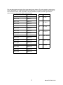
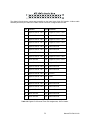
1
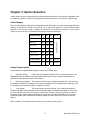
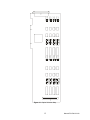
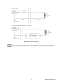
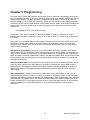
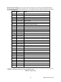
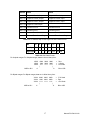
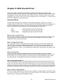
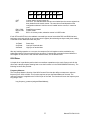
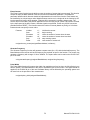
MODEL PCI-DA12-8/16
USER MANUAL
FILE: MPCI-DA12-16.D1q
Notice
The information in this document is provided for reference only. Portwell does not assume any liability
arising out of the application or use of the information or products described herein. This document may
contain or reference information and products protected by copyrights or patents and does not convey
any license under the patent rights of Portwell, nor the rights of others.
IBM PC, PC/XT, and PC/AT are registered trademarks of the International Business Machines
Corporation.
Printed in USA. Copyright 2001, 2005 by Portwell I/O Products Inc. All rights reserved.
WARNING!!
ALWAYS CONNECT AND DISCONNECT YOUR FIELD CABLING WITH
THE COMPUTER POWER OFF. ALWAYS TURN COMPUTER POWER OFF
BEFORE INSTALLING A CARD. CONNECTING AND DISCONNECTING
CABLES, OR INSTALLING CARDS INTO A SYSTEM WITH THE
COMPUTER OR FIELD POWER ON MAY CAUSE DAMAGE TO THE I/O
CARD AND WILL VOID ALL WARRANTIES, IMPLIED OR EXPRESSED.
2
Manual PCI-DA12-8/16
Warranty
Prior to shipment, Portwell equipment is thoroughly inspected and tested to applicable specifications.
However, should equipment failure occur, Portwell assures its customers that prompt service and support
will be available. All equipment originally manufactured by Portwell which is found to be defective will be
repaired or replaced subject to the following considerations.
Terms and Conditions
If a unit is suspected of failure, contact Portwell' Customer Service department. Be prepared to give the
unit model number, serial number, and a description of the failure symptom(s). We may suggest some
simple tests to confirm the failure. We will assign a Return Material Authorization (RMA) number which
must appear on the outer label of the return package. All units/components should be properly packed for
handling and returned with freight prepaid to the Portwell designated Service Center, and will be returned
to the customer's/user's site freight prepaid and invoiced.
Coverage
First Three Years: Returned unit/part will be repaired and/or replaced at Portwell option with no charge for
labor or parts not excluded by warranty. Warranty commences with equipment shipment.
Following Years: Throughout your equipment's lifetime, Portwell stands ready to provide on-site or in-plant
service at reasonable rates similar to those of other manufacturers in the industry.
Equipment Not Manufactured by Portwell
Equipment provided but not manufactured by Portwell is warranted and will be repaired according to the
terms and conditions of the respective equipment manufacturer's warranty.
General
Under this Warranty, liability of Portwell is limited to replacing, repairing or issuing credit (at Portwell
discretion) for any products which are proved to be defective during the warranty period. In no case is Portwell
liable for consequential or special damage arriving from use or misuse of our product. The
customer is responsible for all charges caused by modifications or additions to Portwell equipment not
approved in writing by Portwell or, if in Portwell opinion the equipment has been subjected to abnormal
use. "Abnormal use" for purposes of this warranty is defined as any use to which the equipment is
exposed other than that use specified or intended as evidenced by purchase or sales representation.
Other than the above, no other warranty, expressed or implied, shall apply to any and all such equipment
furnished or sold by Portwell.
3
Manual PCI-DA12-8/16
Table of Contents
Chapter 1: Introduction................................................................................................. 5
Specifications ............................................................................................................ 6
Figure 1-1: Block Diagram ...................................................................................... 8
Chapter 2: Installation................................................................................................... 9
Chapter 3: Option Selection ....................................................................................... 11
Figure 3-1: Option Selection Map.......................................................................... 12
Figure 3-2: Field Wiring Diagram .......................................................................... 13
Chapter 4: Address Selection .................................................................................... 14
Chapter 5: Programming ............................................................................................ 15
Table 5-1: Register Map ........................................................................................ 16
Table 5-2: I/O Address Map for the Digital I/O and Counter/Timers ...................... 17
Table 5-3: DAC Data Format ................................................................................. 17
Table 5-4: I/O Address Table for Digital ................................................................ 18
Table 5-5: Control Register Bit Assignments ......................................................... 18
Chapter 6: 8254 Counter/Timer .................................................................................. 20
Chapter 7: Software .................................................................................................... 25
Chapter 8: Calibration................................................................................................. 26
Chapter 9: Connector Pin Assignments.................................................................... 28
Table 9-1: DAC Pin Assignments, DB37M ............................................................ 28
Table 9-2: Digital I/O & Counter/Timer Pin Assignments, 40-Pin Header.............. 29
Table 9-3: Digital I/O & Counter/Timer Pin Assignments, DB37F.......................... 30
4
Manual PCI-DA12-8/16
Chapter 1: Introduction
Features
•
8 or 16 Channels of Analog Output, 12 Bits Resolution.
•
24 Digital I/O Lines Buffered on the Card.
•
Digital I/O Buffers Can Be Tri-stated under Program Control.
•
Four and Eight Bit Ports Independently Selectable for Input or Output.
•
Pull-Ups on Digital I/O Lines.
•
Resettable fused +5V Supply Available to the User.
•
Three 16-bit 1MHz down-counters, can generate interrupts to clock DACs.
Description
These are full-size cards that can be installed in any PCI slot of PC-AT class computers. They contain
either eight or sixteen double-buffered digital-to-analog converters (DACs) that provide independent
analog output channels of 12-bit resolution. Each analog output channel can be configured for ranges of:
0V to +2.5V
0V to +5V
0V to +10V
-2.5V to +2.5V
-5V to +5V
-10V to +10V
4mA to 20mA sink
The analog output channels have a double-buffered input for single-step update and each is addressed at
its own I/O location. Type AD7237 double-buffered, dual, DAC chips are used. Data are transferred into
outer registers a byte at a time and then transferred into inner registers a word at a time. The analog
outputs can be updated either independently, simultaneously by command, or simultaneously by timer.
The DAC outputs are undefined at power-up. Therefore, in order to prevent excessive voltage output to
external circuits, the card contains automatic circuits that set D/A outputs to less than 15 percent of span
at system power-on. Upon power-up, the card is not in the Simultaneous Update mode. After all DACs
have been loaded with the desired values, a software command can be used to switch the reference
voltage to its normal value. Similarly, a software command can be used at any time to set the reference
voltage to 15 percent causing all DAC outputs to be equal to 15 percent of each DAC’s programmed
value.
These cards contain a type 8255-5 Programmable Peripheral Interface (PPI) chip providing 24 bits of
parallel digital input/output. They can be programmed as inputs or outputs on three 8-bit ports designated
Ports A, B, and C. Port C can be further divided into two 4-bit nibbles.
Each I/O line is buffered by a type 74ABT245B tristate buffer transceiver capable of sourcing 32 mA or
sinking 64mA. Pull-ups on the card assure that there are no erroneous outputs at power up. The buffers
are configured automatically by hardware logic for input or output according to direction assignment from
a control register in the PPI.
5
Manual PCI-DA12-8/16
These cards contain a type 82C54 counter/timer which has three 16-bit programmable down counters.
Counter/Timer #0 and Counter/Timer #1 are configured for event counting. Counter/Timers #1 and #2 are
concatenated and form a 32-bit counter/timer for frequency generation. The dual counter/timer is clocked
by a 1 MHZ crystal oscillator and may be gated on/off by a CMOS level signal at the connector. The
counters can also be programmed to provide a “clock-tick” interrupt and update of the DAC buffers for
more precisely timed outputs.
Specifications
Analog Outputs
•
Resolution:
12 bits (0 to 4095 decimal)
•
Channels:
16 or 8 Voltage output or Current sink channels
•
Current Range:
4 to 20 mA.(with excitation voltage 8-36 VDC)
•
Voltage ranges (5mA max):
0V to +2.5V
0V to +5V
0V to +10V
-2.5V to +2.5V
-5V to +5V
-10V to +10V
AD7237 D/A Converter, Double Buffered / Simultaneous Update
•
Relative Accuracy:
+ ½ LSB
•
Monotonicity:
12 bits over operating temperature range
•
Settling Time:
8 usec to one LSB for full-scale step input
•
Linearity:
+ ½ LSB integral non-linearity over rated temperature range
•
Gain Stability:
15 ppm/ °C
•
Output Drive Capability: 5mA maximum
•
Short-Circuit Current:
25 mA maximum
•
Output Resistance:
Less than 0.1 Ω
•
Data Format:
12-bit binary, right justified, and offset binary for bipolar outputs
Digital I/O
Output (0 to 24 Channels)
•
Logic High:
2.5 VDC min., source 32 mA
•
Logic Low:
0.5 VDC max., sink 64 mA
Input (0 to 24 Channels)
•
Logic High:
2.0 to 5.0 VDC, Input Load: +20 μA
•
Logic Low:
-0.5 to +0.8 VDC, Input Load: -20 μA
6
Manual PCI-DA12-8/16
Counter/Timer
•
Type:
82C54 programmable interval counters
•
Output Drive:
2.2 ma at 0.45 VDC (5 LSTTL loads)
•
Input Gate:
TTL/CMOS compatible
•
Clock:
On-board, 1 MHz crystal-controlled oscillator
•
Active Count Edge:
Negative edge
•
Timer Range:
32 bits
•
Event Counter Range: 16 bits
•
Minimum Clock Pulse Width:
30 ns high, 50 ns low
Environmental
•
Operating Temperature Range: 0 °C. to +60 °C
•
Storage Temperature Range:
-20 °C. to +85 °C
•
Humidity:
5% to 95% non-condensing
•
External DAC Reference (input): +4.5V to +5.5V
•
5V Source (output):
0 to 500 mA, fused (resetting)
•
Size:
12.2" long (310 mm)
•
Power Required:
+12 VDC at 310 mA maximum (16 channels)
-12 VDC at 150 mA maximum
+5 VDC at 662 mA typical with all digital outputs at high impedance
7
Manual PCI-DA12-8/16
DAC 0
PCI
ADDRESS
DECODE
AND
BUS
INTERFACE
OUTER
INNER
DATA
DATA
REGISTER
REGISTER
UPDATE DACS
DAC
12-BIT
DAC # 15
OUTPUT
37
PIN
DACSs 1-14
COMPUTER PCI BUS
C
O
N
N
E
C
T
O
R
RANGE SELECT
OUTER
INNER
DATA
DATA
REGISTER
REGISTER
DAC
12-BIT
DAC # 0
OUTPUT
DAC 15
+12VDC
VREF
RESET
DISABLEOUTPUT
SWITCH
RANGE SELECT
VREF TO ALL DACS
~0.75V
PORT A
PPI
PORT B
GROUP
PORT C HI
0
PORT C LO
I/O
B
U
F
F
E
R
S
PCI
FREQUENCY INPUT
BUS
CONTROL
40
PIN
8254
INPUT
LOGIC
GATE
C
O
N
N
E
C
T
O
R
OUT
CTR0
1MHz OSC
INPUT
GATE
5V
INPUT
GATE
OUT
CTR1
OUT
CTR2
FREQUENCY OUTPUT
PULSE WIDTH INPUT
(GATE)
Figure 1-1: Block Diagram
8
Manual PCI-DA12-8/16
Chapter 2: Installation
A printed Quick-Start Guide (QSG) is packed with the card for your convenience. If you’ve already
performed the steps from the QSG, you may find this chapter to be redundant and may skip forward to
begin developing your application.
The software provided with this card is on CD and must be installed onto your hard disk prior to use. To
do this, perform the following steps as appropriate for your operating system.
Configure Card Options via Jumper Selection
Before installing the card into your computer, carefully read Chapter 3: Option Selection of this manual,
then configure the card according to your requirements. Our Windows based setup program can be used
in conjunction with Chapter 3 to assist in configuring jumpers on the card, as well as provide additional
descriptions for usage of the various card options.
CD Software Installation
The following instructions assume the CD-ROM drive is drive “D”. Please substitute the appropriate drive
letter for your system as necessary.
DOS
1.
2.
3.
4.
Place the CD into your CD-ROM drive.
Type B- to change the active drive to the CD-ROM drive.
Type GLQR?JJ- to run the install program.
Follow the on-screen prompts to install the software for this board.
WINDOWS
1.
Place the CD into your CD-ROM drive.
2.
The system should automatically run the install program. If the install program does not run
promptly, click START | RUN and type BGLQR?JJ, click OK or press -.
3.
Follow the on-screen prompts to install the software for this board.
LINUX
1.
Please refer to linux.htm on the CD-ROM for information on installing under linux.
Caution! * ESD A single static discharge can damage your card and cause premature
failure! Please follow all reasonable precautions to prevent a static
discharge such as grounding yourself by touching any grounded
surface prior to touching the card.
9
Manual PCI-DA12-8/16
Hardware Installation
1.
2.
3.
4.
5.
6.
7.
8.
9.
10.
Make sure to set switches and jumpers from either the Option Selection section of this manual or
from the suggestions of SETUP.EXE.
Do not install card into the computer until the software has been fully installed.
Turn OFF computer power AND unplug AC power from the system.
Remove the computer cover.
Carefully install the card in an available 5V or 3.3V PCI expansion slot (you may need to remove
a backplate first).
Inspect for proper fit of the card and tighten screws. Make sure that the card mounting bracket is
properly screwed into place and that there is a positive chassis ground.
Install an I/O cable onto the card’s bracket mounted connector.
Replace the computer cover and turn ON the computer which should auto-detect the card
(depending on the operating system) and automatically finish installing the drivers.
Run PCIfind.exe to complete installing the card into the registry (for Windows only) and to
determine the assigned resources.
Run one of the provided sample programs that was copied to the newly created card directory
(from the CD) to test and validate your installation.
The base address assigned by BIOS or the operating system can change each time new hardware is
installed into or removed from the computer. Please recheck PCIFind or Device Manager if the hardware
configuration is changed. Software you write can automatically determine the base address of the card
using a variety of methods depending on the operating system. In DOS, the PCI\SOURCE directory
shows the BIOS calls used to determine the address and IRQ assigned to installed PCI devices. In
Windows, the Windows sample programs demonstrate querying the registry entries (created by PCIFind
and NTIOPCI.SYS during boot-up) to determine this same information.
10
Manual PCI-DA12-8/16
Chapter 3: Option Selection
Voltage output ranges are determined by switch settings as described in the following paragraphs. Also,
the method to update D/A outputs is programmable as described here and in Chapter 5, Programming.
Output Ranges
There is a three-position slide switch associated with each DAC channel to make voltage range selection:
switches S1 (Channel 0) through S16 (Channel 15). A silk-screen diagram on the card defines switch
positions to use for each range. In addition to the switch, one jumper per channel is used to select
Voltage vs Current Output. The following table presents the same information:
Voltage Range S1
S2
S3
JP1-16
OFF OFF On
0 to +5V
OFF OFF OFF
0 to +10V
OFF ON
-2.5V to +2.5V
ON
OFF ON
-5V to +5V
ON
OFF OFF
-10V to +10V
ON
ON
OFF
Current Range
S1
S2
S3
4 mA to 20 mA
OFF OFF OFF Position I
OFF
Set in Position V
0 to +2.5V
JP1-16
Analog Output Update
Analog outputs are updated under program control in any of three ways:
Automatic Update:
Each channel is updated individually when new data are written to the
a.
related high-byte base address. Individual update mode may be set by a special read operation as
defined in the programming section of this manual.
b.
Simultaneous Update: The outputs of all D/As may be updated simultaneously. This is done by
first enabling simultaneous updating for all outputs, preloading the low and high bytes of each DAC, and
then initiating a simultaneous update by software command.
c.
Timer Update:
The counter/timer can initiate updates. First, disable interrupts and
updates (read base+4 and read base+6) and enable Simultaneous Updates (read base+0). Then write
the initial values into the DACs. Program the counter/timer for the tick frequency (mode 2 or mode 4),
initialize your ISR, enable updates (read base+5), and enable interrupts (read base+3). This countergenerated update pulse is available at the 40-pin header connector (OUT2) to synchronize external
devices.
Refer to Chapter 5, Programming of this manual for more detail on this process.
11
Manual PCI-DA12-8/16
P2
JP1
JP2
JP3
JP4
JP5
JP6
I
V
S2
S4
S6
S8
S1
S3
S5
S7
JP9
JP10
JP11
JP12
JP13
JP14
JP15
JP16
I
V
S16
S14
S12
S10
S15
S13
S11
S9
P3
Manual PCI-DA12-8/16
12
JP7
JP8
Figure 3-1: Option Selection Map
Vo lta g e Ou tp u t
D AC
Analog
Voltage O utput
5 m A m a xim u m
R
Load
C AR D
A P P L IC ATION
Gro u n d
Current O utput (Jumpers placed in "I” Position)
DA C
A nalog
Current Output
R
Load
Excitation Voltage
8-36 V maximum*
(O bserve Polarity)
G round
Figure 3-2: Field Wiring Diagram
Caution!
Do not connect current loops in a DAC that is set to voltage mode. The loop supply can destroy
the DAC.
13
Manual PCI-DA12-8/16
Chapter 4: Address Selection
These cards use two I/O address spaces, one of 64 bytes and one of 256 bytes. The DACs occupy the
first 32 bytes of the first area. The digital I/O circuit uses the next 4 register locations. The timer/counter
chip uses 4 locations after that. The other 24 addresses are reserved. The 2nd I/O address space of 256
bytes is used for software calibration data. These two I/O address spaces are defined in the Port Address
Selection Table in the Programming section of this manual.
PCI architecture is Plug-and-Play. This means that the BIOS or Operating System determines the
resources assigned to PCI cards rather than you selecting those resources with switches or jumpers. As a
result, you cannot set or change the card's base address or IRQ level. You can only determine what the
system has assigned.
To determine the base address that has been assigned, run the PCIFind.EXE utility program provided.
This utility will display a list of all of the cards detected on the PCI bus, the addresses assigned to each
function on each of the cards, and the respective IRQs.
Alternatively, some operating systems can be queried to determine which resources were assigned. In
these operating systems, you can use either PCIFind or the Device Manager utility from the System
Properties Applet of the control panel. The card is installed in the Data Acquisition class of the Device
Manager list. Selecting the card, clicking Properties, and then selecting the Resources Tab will display a
list of the resources allocated to the card.
PCIFind uses the Vendor ID and Device ID to search for your card, then reads the base address and
IRQ.
If you want to determine the base address and IRQ yourself, use the following information.
The Vendor ID for these cards is 494F. (ASCII for "IO".) V stands for Voltage Only.
The Device ID for the 8 channel card is 6CA8h.
The Device ID for the 16 channel card is 6CB0h.
The Device ID for the 8 channel V card is 6CA9h.
The Device ID for the 16 channel V card is 6CB1h.
The control / DAC / I/O / Counter/Timer base address is BaseAddresses[2] in the
PCI_COMMON_CONFIG structure, while the calibration base address is BaseAddresses[3].
14
Manual PCI-DA12-8/16
Chapter 5: Programming
The cards’ DACs, Timers, and Digital I/O use 40 consecutive I/O addresses. Programming these cards is
very straightforward as there are only three operating modes, three range-selection switches per channel,
and one unique addition. The basic operation of a Digital-to-Analog card is to write a 12-bit value to a
Digital to Analog Converter (DAC) pre-load (outer) register where it is buffered and loaded by an update
command to a DAC (inner) register. Outputs of that register control a "ladder" network which produces the
analog output. The output voltage range is defined by settings of the range-selection switches for that
channel. In C:
outport(BASE+(CH*2), (Volts*4096/10)-2048);
would output "Volts" volts to channel "ch", assuming a bipolar 5V range. For other bipolar ranges,
substitute the appropriate voltage span in place of "10" in the equation. For unipolar ranges, also remove
the "-2048".
Upon power-up, or hardware reset, the DAC registers are restricted to a safe value and the card is set in
Simultaneous Update mode. Since the pre-load register is not cleared upon power-up, but left at an
undefined value, a known value must be written to the preload registers before using a "Clear RestrictOutput-Voltage" command.
Simultaneous Update Mode is the power-up or default mode of operation for the DAC card. When a
value is written to a DAC address the output does not change until an output update is commanded via a
read from Base Address+8. (Alternatively, a read of Base Address+A will update the DAC registers and
switch the board to Automatic Update Mode.) While in Simultaneous Update Mode, a single read will load
all DAC registers with the value waiting in the pre-load registers, causing all outputs to be updated and
changed simultaneously.
Automatic Update Mode is the configuration that changes a DAC output immediately after the high-byte
of the new value is written to the DAC address. If the card is in Simultaneous Update Mode a read of
Base Address+2 will change the card back to Automatic Update Mode without updating the outputs. A
read of Base Address+A will update all outputs simultaneously and then place the card in Automatic
Update Mode.
Timer Update Mode is similar to Simultaneous Update Mode, except that updates are issued by the
counter/timer (programmed in mode 2 or mode 4 per Chapter 6, Programming 8254). A read from Base
Address+5 will change the card from Simultaneous Update Mode to Timer Update Mode, and a read from
Base Address+6 will change it back. The counter-generated update pulse is also available at the 40-pin
header connector(OUT2) to synchronize external devices, and can generate interrupts for synchronized
loading if enabled by a read from Base Address+3. (Interrupts are disabled by a read from Base
Address+4.)
15
Manual PCI-DA12-8/16
Restrict-Output-Voltage limits the output of all DAC channels. This is done by reading Base Address
+E. The previous outputs will be restored when a "Clear Restrict-Output-Voltage" command is issued by a
read of Base Address+F.
Address Write *
Read
Base + 0
DAC 0 Low Byte
Place card in Simultaneous Mode without updating outputs.
Base + 1
DAC 0 High Byte
Base + 2
DAC 1 Low Byte
Release card from Simultaneous Mode without updating outputs.
Base + 3
DAC 1 High Byte
Enable Interrupts
Base + 4
DAC 2 Low Byte
Disable Interrupts
Base + 5
DAC 2 High Byte
Enable Timer-Initiated DAC Update
Base + 6
DAC 3 Low Byte
Disable Timer-Initiated DAC Update
Base + 7
DAC 3 High Byte
Base + 8
DAC 4 Low Byte
Base + 9
DAC 4 High Byte
Base + A
DAC 5 Low Byte
Base + B
DAC 5 High Byte
Base + C
DAC 6 Low Byte
Base + D
DAC 6 High Byte
Base + E
DAC 7 Low Byte
Restrict-Output-Voltage (Limits outputs to 15% of full scale range).
Base + F
DAC 7 High Byte
Clear Restrict-Output-Voltage (Allows full operating output voltage).
Base + 10
DAC 8 Low Byte
Base + 11
DAC 8 High Byte
Base + 12
DAC 9 Low Byte
Base + 13
DAC 9 High Byte
Base + 14
DAC 10 Low Byte
Base + 15
DAC 10 High Byte
Base + 16
DAC 11 Low Byte
Base + 17
DAC 11 High Byte
Base + 18
DAC 12 Low Byte
Base + 19
DAC 12 High Byte
Base + 1A
DAC 13 Low Byte
Base + 1B
DAC 13 High Byte
Base + 1C
DAC 14 Low Byte
Base + 1D
DAC 14 High Byte
Base + 1E
DAC 15 Low Byte
Base + 1F
DAC 15 High Byte
Update all outputs and place card in Simultaneous Mode.
Update all outputs and release card from Simultaneous Mode.
Clear IRQ
* Although it is possible to write the low and high bytes separately as shown above, it is much easier to write both bytes with a
single OUT DX, AX instruction. In that case, only even addresses are written.
Table 5-1: Register Map
16
Manual PCI-DA12-8/16
Address
Write
Read
Base + 20 Digital I/O Port A, Output
Digital I/O Port A, Input
Base + 21 Digital I/O Port B, Output
Digital I/O Port B, Input
Base + 22 Digital I/O Port C, Output
Digital I/O Port C, Input
Base + 23 Digital I/O Control Byte
Base + 24 Counter/Timer 0
Counter/Timer 0
Base + 25 Counter/Timer 1
Counter/Timer 1
Base + 26 Counter/Timer 2
Counter/Timer 2
Base + 27 Counter/Timer Control Register
Counter/Timer Control Register
Table 5-2: I/O Address Map for the Digital I/O and Counter/Timers
BIT
D7 D6 D5 D4 D3
D2
D1
D0
Low Byte
B7 B6 B5 B4 B3
B2
B1
B0
B10
B9
B8
High Byte x
x
x
x
B11
Table 5-3: DAC Data Format
For Unipolar ranges: For Unipolar ranges, data are in true binary form.
XXXX
XXXX
XXXX
MSB or B11
0000
1000
1111
|
0000
0000
1111
0000
0000
1111
|
Å
=
=
=
Æ
Zero
½ Scale
Full Scale
B0 or LSB
For Bipolar ranges: For Bipolar ranges, data are in offset binary form.
XXXX
XXXX
XXXX
MSB or B11
0000
1000
1111
|
0000
0000
1111
Å
0000
0000
1111
|
=
=
=
Æ
17
-Full Scale
Zero
+Full Scale
B0 or LSB
Manual PCI-DA12-8/16
Programming the Digital I/O Circuit
The digital I/O circuit is comprised of an Intel 8255, a direction control latch, and four bi-directional buffers
with 10K pull-ups. Please refer to the 8255-5 specification in Appendix A for a detailed description of the
PPI.
Address
Assignment
Operation
Base Address +20
Port A
Read/Write
Base Address +21
Port B
Read/Write
Base Address +22
Port C
Read/Write
Base Address +23
Control
Read/Write
Table 5-4: I/O Address Table for Digital
The circuit is designed to use the PPI in mode 0 wherein:
a.
b.
c.
d.
There are two 8-bit ports (A and B) and two 4-bit ports (C Hi and C Lo).
Any port can be configured as an input or an output.
Outputs are latched.
Inputs are not latched.
The 8-bit control register is used to set the mode and direction of the ports.
Bit
Assignment
Function
D0
Port C Lo (C0-C3)
1 = Input, 0 = Output
D1
Port B
1 = Input, 0 = Output
D2
Mode Selection
1 = Mode 1, 0 = Mode 0
D3
Port C Hi (C4-C7)
1 = Input, 0 = Output
D4
Port A
1 = Input, 0 = Output
D5,D6
Mode Selection
01 = Mode 1, 00 = Mode 0 1X = Mode 2
D7
Mode Set Flag&Tristate
1 = Active & Tristate
Table 5-5: Control Register Bit Assignments
Note
PPI Mode 1 cannot be used with this circuit without modification. Thus, bits D2, D5, and D6 should
always be set to "0". If your card has been modified to operate in Mode 1, then there is an Addendum
sheet in the front of this manual describing that modification. This circuit cannot be modified to operate in
PPI Mode.
The circuit is initialized by the computer Reset command (all ports set for input and all buffers enabled).
Both the 8255 control register and the buffer direction latch are accessed at the same address.
The 8255 control register will latch a new configuration byte when it's written to with bit D7 high. If, for
example, hex 80 is sent to Base Address+23, the group 0 PPI will be configured in mode 0 with ports A,
B, and C as outputs.
18
Manual PCI-DA12-8/16
At the same time, data bit D7 is also latched in the buffer controller. A high state puts the buffers in the
tristate mode; i.e., disabled. Now, if any of the ports are to be set as outputs, you may set the values of
the respective port with the outputs still in tristate condition. Lastly, to enable the ports a control byte with
bit D7 low must be sent to Base Address+23.
Note
All data bits except D7 must be the same for the two control bytes. Those buffers will now remain enabled
until another control byte with data bit D7 high is sent to Base Address+23.
19
Manual PCI-DA12-8/16
Chapter 6: 8254 Counter/Timer
These cards contain a type 8254 programmable counter/timer that allows you to implement such
functions as a Real Time Clock, Event Counter, Digital One-Shot, Programmable Rate Generator, Binary
Rate Multiplier, Complex Wave Generator and/or a Motor Controller. The 8254 consists of three, 16-bit,
presettable, down counters. Each counter can be programmed to any count between 1 or 2 and 65,535 in
binary format depending on the mode chosen.
Operational Modes
The 8254 modes of operation are described in the following paragraphs to familiarize you with the
versatility and power of this device. For those interested in more detailed information, a full description of
the 8254 programmable interval timer can be found in the Intel (or equivalent manufacturers') data
sheets. The following conventions apply for use in describing operation of the 8254 :
Clock:
Trigger:
Counter Loading:
A positive pulse into the counter's clock input
A rising edge input to the counter's gate input
Programming a binary count into the counter
Mode 0: Pulse on Terminal Count
After the counter is loaded, the output is set low and will remain low until the counter decrements to zero.
The output then goes high and remains high until a new count is loaded into the counter. A trigger
enables the counter to start decrementing.
Mode 1: Retriggerable One-Shot
The output goes low on the clock pulse following a trigger to begin the one-shot pulse and goes high
when the counter reaches zero. Additional triggers result in reloading the count and starting the cycle
over. If a trigger occurs before the counter decrements to zero, a new count is loaded. This forms a
retriggerable one-shot. In mode 1, a low output pulse is provided with a period equal to the counter countdown time.
Mode 2: Rate Generator
This mode provides a divide-by-N capability where N is the count loaded into the counter. When
triggered, the counter output goes low for one clock period after N counts, reloads the initial count, and
the cycle starts over. This mode is periodic, the same sequence is repeated indefinitely until the gate
input is brought low. This mode also works well as an alternative to mode 0 for event counting.
Mode 3: Square Wave Generator
This mode operates like mode 2. The output is high for half of the count and low for the other half. If the
count is even, then the output is a symmetrical square wave. If the count is odd, then the output is high
for (N+1)/2 counts and low for (N-1)/2 counts. Periodic triggering or frequency synthesis are two possible
applications for this mode. Note that in this mode, to achieve the square wave, the counter decrements by
two for the total loaded count, then reloads and decrements by two for the second part of the wave form.
Mode 4: Software Triggered Strobe
This mode sets the output high and, when the count is loaded, the counter begins to count down. When
the counter reaches zero, the output will go low for one input period. The counter must be reloaded to
repeat the cycle. A low gate input will inhibit the counter.
20
Manual PCI-DA12-8/16
Mode 5: Hardware Triggered Strobe
In this mode, the counter will start counting after the rising edge of the trigger input and will go low for one
clock period when the terminal count is reached. The counter is retriggerable. The output will not go low
until the full count after the rising edge of the trigger.
Programming the 8254
On these cards, the 8254 counters occupy the following addresses (hex):
Base Address + 24:
Base Address + 25:
Base Address + 26:
Base Address + 27:
Read/Write Counter #0
Read/Write Counter #1
Read/Write Counter #2
Write to Counter Control register
The counters are programmed by writing a control byte into a counter control register at Base Address +
27. The control byte specifies the counter to be programmed, the counter mode, the type of read/write
operation, and the modulus. The control byte format is as follows:
B7
B6
B5
B4
B3
B2
B1
B0
SC1 SC0 RW1 RW0 M2
M1
M0
BCD
SC0-SC1: These bits select the counter that the control byte is destined for.
SC1
SC0
Function
0
0
Program Counter #0
0
1
Program Counter #1
1
0
Program Counter #2
1
1
Read/Write Cmd.*
* See section on Reading and Loading the Counters.
RW0-RW1: These bits select the read/write mode of the selected counter.
RW1
RW0
Counter Read/Write Function
0
0
Counter Latch Command
0
1
Read/Write LS Byte
1
0
Read/Write MS Byte
1
1
Read/Write LS Byte, then MS Byte
21
Manual PCI-DA12-8/16
M0-M2: These bits set the operational mode of the selected counter.
Mode
M2
M1
M0
0
0
0
0
1
0
0
1
2
X
1
0
3
X
1
1
4
1
0
0
5
1
0
1
BCD: Set the selected counter to count in binary (BCD = 0) or BCD (BCD = 1).
Reading and Loading the Counters
If you attempt to read the counters on the fly when there is a high input frequency, you will most likely get
erroneous data. This is partly caused by carries rippling through the counter during the read operation.
Also, the low and high bytes are read sequentially rather than simultaneously and, thus, it is possible that
carries will be propagated from the low to the high byte during the read cycle.
To circumvent these problems, you can perform a counter-latch operation in advance of the read cycle.
To do this, load the RW1 and RW2 bits with zeroes. This instantly latches the count of the selected
counter (selected via the SC1 and SC0 bits) in a 16-bit hold register. (An alternative method of latching
counter(s) that has an additional advantage of operating simultaneously on several counters is through a
readback command to be discussed later.) A subsequent read operation on the selected counter returns
the held value. Latching is the best way to read a counter on the fly without disturbing the counting
process. You can only rely on directly read counter data if the counting process is suspended by bringing
the gate low.
For each counter you must specify in advance the type of read or write operation that you intend to
perform. You have a choice of loading/reading (a) the high byte of the count, or (b) the low byte of the
count, or (c) the low byte followed by the high byte. This last is most generally used and is selected for
each counter by setting the RW1 and RW0 bits to ones. Subsequent read/load operations must be
performed in pairs in this sequence or the sequencing flip-flop in the 8254 chip will get out of step.
The readback command byte format is:
B7 B6
1
1
B5
B4
B3
B2
B1
B0
CNT STA C2
C1
C0
0
CNT:
When 0, latches the counters selected by bits C0-C2.
STA:
When 0, returns the status byte of counters selected by C0-C2.
C0, C1, C2:
When high, select a particular counter for readback. C0 selects Counter 0, C1
selects Counter 1, and C2 selects Counter 2.
You can perform two types of operations with the readback command. When CNT=0, the counters
selected by C2 through C0 are latched simultaneously. When STA=0, the counter status byte is read
when the counter I/O location is accessed. The counter status byte provides information about the current
output state of the selected counter and its configuration. The status byte returned if STA=0 is:
22
Manual PCI-DA12-8/16
B7
OUT:
NC:
RW1, RW0:
M2, M1, M0:
BCD:
B6
B5
B4
B3
B2
B1
B0
OUT NC RW1 RW2 M2
M1
M0
BCD
Current state of counter output pin.
Null count. This indicates when the last count loaded into the counter register has
been loaded into the actual counter. The exact time of load depends on the
configuration selected. Until the count is loaded into the counter, it cannot be
read.
Read/Write command.
Counter mode.
BCD = 0 is binary mode, otherwise counter is in BCD mode.
If both STA and CNT bits in the readback command byte are set low and the RW1 and RW0 bits have
both been previously set high in the counter control register (thus selecting two-byte reads), then reading
a selected counter address location will yield:
1st Read:
2nd Read:
3rd Read:
Status byte
Low byte of latched data
High byte of latched data
After any latching operation on a counter, the contents of its hold register must be read before any
subsequent latches of that counter will have any effect. If a status latch command is issued before the
hold register is read, then the first read will read the status, not the latched value.
8254 Driver
A simple driver is provided to perform basic counter/timer operations on the cards. Source code for the
driver and a sample program showing how to use the functions is in the DOS\CSAMPLES directory. The
following functions are provided:
Frequency Measure
The Frequency Measure function of the 8254 Counter Driver has the ability to measure an unknown
frequency from 1KHz to 2MHz. This function requires as input the Base Address of the card. The
unknown frequency is applied to the CLOCK IN pin of the card. The function will return the frequency as a
long integer in Hz.
long frequency_measure(unsigned BaseAddress);
23
Manual PCI-DA12-8/16
Event Counter
The Event Counter function has the ability to trace the number of events that have occurred. This function
accepts as input the Base Address of the card, as well as an additional parameter. The additional
parameter identifies which features should be implemented on this call to the function. Each feature can
be identified by its unique integer value. Multiple features can be run in a single call to the function by OR
ing the respective integer values together. Features will be executed in increasing integer order. The
CLOCK IN pin of the card is the point of application for the incoming events. (Note: This function is limited
by the input speed of the 8254 counter, and slow signals are preferred. Further only 65,535 events are
possible without a RESET.) The function returns the number of events (based on priority) or 0 for those
features that do not specify a return value.
Features:
Initialize
Start
Sincestart
Sincelast
Stop
Reset
= 1;
= 2;
= 4;
= 8;
= 16;
= 32;
initialize the counter.
begin counting.
return the number of events since the start.
return the number of events since last check.
stop counting events.
reset number of events to 0.
unsigned event_counter(unsigned BaseAddress, int feature);
Generate Frequency
The Generate Frequency function will generate a square wave (0 to +5V) with the desired frequency. The
Base Address of the card as well as the frequency are required as input to the function. The counter can
generate a frequency with a range of 1Hz to 250KHz. The square wave can be read on the CLOCK OUT
pin of the card.
void generatefrequency(unsigned BaseAddress, unsigned long frequency);
Pulse Width
The Pulse Width function will measure the width of an applied event from its rise to its fall (effectively one
half the period). The Base Address of the card is required as input to the function. The signal should be
applied to the CLOCK IN pin of the card. Software latency will be affected by the operating system and
will set a limit on the precision of the measurement.
unsigned pulse_width(unsigned BaseAddress);
24
Manual PCI-DA12-8/16
Chapter 7: Software
These cards are straightforward to program. The following example is in C, but sample code is also
provided on the CD in Pascal and four Windows languages: C++Builder, Delphi, VisualBASIC, and Visual
C++.
To output an analog value with 12-bit resolution, a corresponding decimal number N between 0 and 4095
is calculated (212 = 4096).
N/4096 = V(out)/V(full scale)
Next the data are written to the selected analog output channel. (See the preceding I/O Address Map.) In
this example, we will assume analog output on channel zero (AO 0).
outport (BASE + 0, N)
For simplicity, it was assumed that the simultaneous-update capability was not used.
Examples of this routine are found on the sample disk along with examples in other languages.
25
Manual PCI-DA12-8/16
Chapter 8: Calibration
Periodic calibration of these cards is recommended if they are used in extreme environmental conditions.
The card uses very stable components but high-low temperature cycles might result in slight analog
output errors.
This card is calibrated by software using the following formula:
Y= (4096 -a - b)/4096) * X + b
To calibrate the card, run the calibration program and follow the screen prompts. No attempt at calibration
should be made in noisy locations or with a noisy calibration setup.
The calibration program stores various data to the card to facilitate calibrating the data output in a runtime environment. The data collected during calibration is stored in an EEPROM located at the second of
the I/O base addresses assigned to the device (BaseAddresses[3] in the PCI_COMMON_CONFIG
structure). The EEPROM contains two values per channel per range. The ZERO (or OFFSET) and the
SPAN calibration constants are stored (a and b from the equation above) for each channel at each
possible range (0-6). These constants are used during normal operation to calibrate the output data in
real-time. Refer to the samples provided on disk for an example of using this data.
In addition to 'a' and 'b' as shown above, the EEPROM contains a table of ranges assigned to each
channel. Starting at Base+F0, 16 base addresses contain one byte each, from 0-6, indicating the voltage
output range assigned to that channel. It is important to use the calibration program at least once if the
default range (+/- 10V) is changed on any channel, to allow this table of data to be reconfigured. If this
data is incorrect, calibration is not guaranteed.
Offset
Span
(‘b’ in formula) (‘a’ in formula)
Word Address
Range
Base + 00h
to
Base + 1Eh
0 to +5 V.
DAC 0
to
DAC 15
DAC 0
to
DAC 15
Base + 20h
to
Base + 3Eh
0 to +2.5 V.
DAC 0
to
DAC 15
DAC 0
to
DAC 15
Base + 40h
to
Base + 5Eh
0 to +10 V.
DAC 0
to
DAC 15
DAC 0
to
DAC 15
Base + 60h
to
Base + 7Eh
-5 V to +5 V.
DAC 0
to
DAC 15
DAC 0
to
DAC 15
Base + 80h
to
Base + 9Eh
-2.5 V to 2.5 V.
DAC 0
to
DAC 15
DAC 0
to
DAC 15
Base + A0h
to
Base + BEh
-10 V to 10 V.
DAC 0
to
DAC 15
DAC 0
to
DAC 15
DAC 0
to
DAC 15
DAC 0
to
DAC 15
Base + C0h
to
Base + DEh
4 to 20 mA.
26
Manual PCI-DA12-8/16
The next table shows the location of the range data for each channel. The value stored is a number from
0 to 6, representing the 7 ranges (as shown in the table below). If you set any channel's range switch, be
sure to place the correct value in this table. Using the calibration program provided is generally the
easiest method of ensuring the table remains accurate.
Word Address
Channel
Base + F0h
Channel 0
Base + F1h
Channel 1
Base + F2h
Channel 2
Base + F3h
Channel 3
Base + F4h
Channel 4
Base + F5h
Channel 5
Base + F6h
Channel 6
Base + F7h
Channel 7
Base + F8h
Channel 8
Base + F9h
Channel 9
Base + FAh
Channel 10
Base + FBh
Channel 11
Base + FCh
Channel 12
Base + FDh
Channel 13
Base + FEh
Channel 14
Base + FFh
Channel 15
27
Value
Range
0
0-5V
1
0 - 2.5 V
2
0 - 10 V
3
-5 - +5 V
4
-2.5 - +2.5V
5
-10 V - +10 V
6
4-20mA
Manual PCI-DA12-8/16
Chapter 9: Connector Pin Assignments
The analog outputs are accessible via a male 37-pin D type connector.
Pin
Name
Function
Pin Name
Function
1
D/A 0 Out
Analog DAC 0 Output
18
Analog GND Analog Ground
2
D/A 1 Out
Analog DAC 1 Output
19
Return GND
Return Analog Ground
3
D/A 2 Out
Analog DAC 2 Output
20
Return GND
Return Analog Ground
4
D/A 3 Out
Analog DAC 3 Output
21
Return GND
Return Analog Ground
5
D/A 4 Out
Analog DAC 4 Output
22
Return GND
Return Analog Ground
6
D/A 5 Out
Analog DAC 5 Output
23
Return GND
Return Analog Ground
7
D/A 6 Out
Analog DAC 6 Output
24
Return GND
Return Analog Ground
8
D/A 7 Out
Analog DAC 7 Output
26
Return GND
Return Analog Ground
9
D/A 8 Out
Analog DAC 8 Output
27
Return GND
Return Analog Ground
10
D/A 9 Out
Analog DAC 9 Output
28
Return GND
Return Analog Ground
11
D/A 10 Out
Analog DAC 10 Output
29
Return GND
Return Analog Ground
12
D/A 11 Out
Analog DAC 11 Output
30
Return GND
Return Analog Ground
13
D/A 12 Out
Analog DAC 12 Output
31
Return GND
Return Analog Ground
14
D/A 13 Out
Analog DAC 13 Output
32
Return GND
Return Analog Ground
15
D/A 14 Out
Analog DAC 14 Output
33
Return GND
Return Analog Ground
16
D/A 15 Out
Analog DAC 15 Output
34
Return GND
Return Analog Ground
17
XREF IN
External Ref In
35
Return GND
Return Analog Ground
36
+5 Vout
37
Power GND
Fused +5 VDC from PC
Power Ground
Table 9-1: DAC Pin Assignments, DB37M
28
Manual PCI-DA12-8/16
The digital I/O and counter outputs are accessible on the board via a 40-pin IDC header. A ribbon cable
assembly with a 40-pin header and a DB37 female connector is shipped with the card.
Pin Function
Pin
Function
1
Digital I/O Port A - Bit 0
21
Digital I/O Port C - Bit 0
2
Digital I/O Port A - Bit 1
22
Digital I/O Port C - Bit 1
3
Digital I/O Port A - Bit 2
23
Digital I/O Port C - Bit 2
4
Digital I/O Port A - Bit 3
24
Digital I/O Port C - Bit 3
5
Digital I/O Port A - Bit 4
25
Return Ground
6
Digital I/O Port A - Bit 5
26
Return Ground
7
Digital I/O Port A - Bit 6
27
Digital I/O Port C - Bit 4
8
Digital I/O Port A - Bit 7
28
Digital I/O Port C - Bit 5
9
Return Ground
29
Digital I/O Port C - Bit 6
10
Return Ground
30
Digital I/O Port C - Bit 7
11
Digital I/O Port B - Bit 0
31
Return Ground
12
Digital I/O Port B - Bit 1
32
Return Ground
13
Digital I/O Port B - Bit 2
33
Clock In
14
Digital I/O Port B - Bit 3
34
Gate
15
Digital I/O Port B - Bit 4
35
Clock Out
16
Digital I/O Port B - Bit 5
36
Return Ground
17
Digital I/O Port B - Bit 6
37
Return Ground
18
Digital I/O Port B - Bit 7
38
Return Ground
19
Return Ground
39
Return Ground
20
Return Ground
40
Return Ground
Table 9-2: Digital I/O & Counter/Timer Pin Assignments, 40-Pin Header
29
Manual PCI-DA12-8/16
Pin
Function
Pin
Function
1
Digital I/O Port A - Bit 0
2
Digital I/O Port A - Bit 2
20
Digital I/O Port A - Bit 1
3
Digital I/O Port A - Bit 4
21
Digital I/O Port A - Bit 3
4
Digital I/O Port A - Bit 6
22
Digital I/O Port A - Bit 5
5
Return Ground
23
Digital I/O Port A - Bit 7
6
Digital I/O Port B - Bit 0
24
Return Ground
7
Digital I/O Port B - Bit 2
25
Digital I/O Port B - Bit 1
8
Digital I/O Port B - Bit 4
26
Digital I/O Port B - Bit 3
9
Digital I/O Port B - Bit 6
27
Digital I/O Port B - Bit 5
10
Return Ground
28
Digital I/O Port B - Bit 7
11
Digital I/O Port C - Bit 0
29
Return Ground
12
Digital I/O Port C - Bit 2
30
Digital I/O Port C - Bit 1
13
Return Ground
31
Digital I/O Port C - Bit 3
14
Digital I/O Port C - Bit 4
32
Return Ground
15
Digital I/O Port C - Bit 6
33
Digital I/O Port C - Bit 5
16
Return Ground
34
Digital I/O Port C - Bit 7
17
Clock In
35
Return Ground
18
Clock Out
36
Gate
19
Return Ground
37
Return Ground
Table 9-3: Digital I/O & Counter/Timer Pin Assignments, DB37F
30
Manual PCI-DA12-8/16
Customer Comments
If you experience any problems with this manual or just want to give us some feedback, please email us
at: [email protected]. Please detail any errors you find and include your mailing address so that
we can send you any manual updates.
31
Manual PCI-DA12-8/16