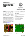
1
NCP1030GEVB
Isolated 2 W Bias Supply for
Telecom Systems Using the
NCP1030 Evaluation Board
User's Manual
http://onsemi.com
EVAL BOARD USER’S MANUAL
Introduction
• Proprietary Active Leading Edge Blanking (LEB)
Power converters using secondary side controllers
provide better transient response, higher efficiency and
usually require less components than their primary side
referenced counterparts. However, secondary side
controllers require a primary side referenced bias supply to
start operation. After start−up, the controller power can be
provided from the secondary side.
The NCP1030 incorporates in a single IC all the active
power, control logic and protection circuitry required for
implementing, with a minimum of external components, a
highly integrated isolated bias supply. The features included
in the NCP1030 can result in a footprint area reduction by up
to 91% compared to a solution implemented using discrete
components.
The NCP1030 Power Switch Circuit is rated at 200 V,
making it ideal for 48 V Telecom and 42 V automotive
applications. In addition, this IC can operate from an
existing 12 V supply. The NCP1030 includes an extensive
set of features including:
• On Board Power Switch: Eliminates the need for an
external switch. As the Power Switch characteristics
are well known the gate drive is tailored to control
switching transitions and help reduce electromagnetic
interference (EMI).
• An Internal Start−up Regulator: Provides power to
the NCP1030 during start−up. After start−up, the
regulator is disabled, thus reducing power consumption.
The regulator can be powered directly from the input
line.
• Internal Error Amplifier: Allows the implementation
of an isolated supply using primary side regulation
without the need for an optocoupler.
• Internal Cycle by Cycle Current Limit: Eliminates
the need for external sensing components. The
programmed current limit is 500 mA.
•
•
•
Design Specifications
An isolated bias supply for a telecom system is designed
and implemented using the NCP1030. The supply delivers
2.0 W at 12 V. The converter specifications are listed in
Table 1.
Table 1. BIAS SUPPLY SPECIFICATIONS
Parameter
Symbol
Min
Max
Input Voltage
Vin
35 V
76 V
Frequency
İ
250 kHz
300 kHz
Peak Efficiency
h
80%
−
Output Voltage
Vout
10.8 V
13.2 V
Output Current
Iout
0.017 A
0.17 A
Output Power
Pout
2.0 W
−
A Flyback topology operating in discontinuous mode is
selected because of its simplicity and low part count.
www.BDTIC.com/ON/
© Semiconductor Components Industries, LLC, 2012
June, 2012 − Rev. 1
•
Circuit: Provides better current limit control compared
to a fixed blanking period. The active LEB circuit
masks the current signal during the Power Switch turn
ON transition.
Individual Line Undervoltage and Overvoltage
(UV/OV) Detectors with Hysteresis: Eliminate the
need for external supervisory function. The UV/OV
detectors can be disabled if not needed.
Single Capacitor Oscillator: Eliminates traditional
timing resistor. Oscillator is optimized for operation up
to 1.0 MHz.
Internal $2% Voltage Reference: Eliminates the
need for an external bypass capacitor.
Thermal Shutdown Circuit: Protects the device in the
event the maximum junction temperature is exceeded.
1
Publication Order Number:
EVBUM2126/D
NCP1030GEVB
Flyback Converter
relates the on−time volt−second product to the reset
volt−second product and adds a 20% dead time to insure the
converter operates in discontinuous mode. Solving
Equation 2 assuming a 0.5 V drop across D1,
A dual output Flyback converter is shown in Figure 1.
OUTPUT 1 is regulated by means of OUTPUT 2, providing
an isolated OUTPUT 1 without the need for an optocoupler.
TX
Np
D1
+
Ns
Cout
+
−
−
D2
Snubber
CCC
VCC (OUTPUT2)
−
R1
EA
+
VREF
R2
−
Figure 1. Isolated Flyback Converter
Current flows in the primary side when the Power Switch,
M1, is ON. The transformer primary side dot end becomes
positive with respect to the non−dot end. While the Power
Switch is ON, energy is stored in the transformer and D1 and
D2 are reverse biased. When M1 turns OFF, the transformer
winding polarities are reversed, forward biasing D1 and D2.
Energy is transferred to the secondary outputs during this
period. If the secondary current decays to zero before the
switch turns ON again, the converter operates in
discontinuous mode. Otherwise, it operates in continuous
mode.
The converter regulates the output by sampling the output
voltage and comparing it to a reference voltage. A signal
proportional to their difference is generated and used to
adjust the ON time of M1 such that the voltage difference is
reduced.
The Snubber limits the voltage across the Power Switch
and helps reduce noise.
Parameter
Ns
(Vin * (IPPK
(Vout ) VfD1)
(0.8 * DC)
Min
Max
1,2−3,4
102 mH
−
Leakage Inductance
1,2−3,4
−
0.955 mH
1−4
2−3
5−6
7−8
−
−
−
−
0.655 W
0.82 W
0.248 W
0.248 W
Cout +
−
3.8 MHz (typ.)
Iout
f
(1 * DC)
Vdroop
(eq. 5)
Solving Equation 5, a maximum voltage droop of 50 mV
requires a 7.4 mF capacitor. However, Cout may be increased
to facilitate frequency compensation.
The secondary peak current, ISPK, and the diode blocking
voltage, Vblock, determine the selection of rectification
diodes, D1 and D2.
The primary peak current and transformer turns ratio
determine the secondary peak current as given by
Equation 6.
(eq. 1)
DC
(Vout ) VfD1) (eq. 4)
Two main factors, voltage ripple and frequency
compensation, are considered for the selection of the output
capacitor, Cout. This section will focus on voltage ripple,
while frequency compensation is covered in a latter section.
The output capacitor provides the load current during the
switch ON time. If the target voltage droop is known, Cout
is calculated using Equation 5.
ǒNp
Ǔ is calculated
Ns
RDS(on)))
Ns
Main Output
using Equation 2
w
Np
Terminals
Resonant Frequency
Solving Equation 1, a primary inductance of 127 mH is
Np
(eq. 3)
Magnetizing
Inductance @ 0.4 A
DC Resistance
The converter is designed to operate at a maximum duty
cycle (DC) of 40 % and a primary peak current (IPPK) of
400 mA. The required primary inductance, LP, is calculated
using Equation 1.
V
DC
Lp + in(min)
f IPPK
0.4
Table 2. TRANSFORMER SPECIFICATIONS
Design Procedure
required. The transformer turns ratio
(0.8 * 0.4)
The voltage is significantly below the 200 V maximum
rating of the NCP1030 internal Power Switch.
The transformer winding arrangement includes a split
primary with bifilar secondaries. The transformer can be
ordered from Coilcraft under part number B0226−E. Table 2
summarizes the specifications of the transformer.
+
M1
7 W))
(12 V ) 0.5 V)
Vstress + Vin(max) )
−
PWM
Controller
(35 V * (0.4 A
a turns ratio greater than 2.58 is required. A turns ratio of
2.78 is selected.
A maximum stress voltage of 110 V across the primary
switch during the turn OFF period is calculated using
Equation 4.
Vout (OUTPUT1)
+
Vin
w
(eq. 2)
ISPK + IPPK
where, VƒD1 is the forward voltage drop across D1 and
RDS(on) is the Power Switch on resistance. Equation 2
Np
Ns
www.BDTIC.com/ON/
http://onsemi.com
2
(eq. 6)
NCP1030GEVB
The voltage across the rectification diode is given by
Equation 7.
+
ǒNNpsǓ
Cout
Rout Vout
−
(eq. 7)
+
Vblock + Vout ) Vin(max)
D1
TX
Solving Equations 6 and 7, the rectification diode needs
to handle 1.11 A and 39.34 V. In addition to the voltage
calculated using equation 7, voltage spikes during switching
transitions need to be considered when selecting the
blocking voltage rating. A Schottky diode is selected to
reduce the forward voltage drop, thus reducing power
dissipation. On Semiconductor’s MBRA160 is selected as it
meets all the requirements.
B
D2
Vin
−
RESR
Rout(eq)
Cout(eq)
Z1
A
Zf
−
PWM
Controller
EA
+
+
Auxiliary Supply Regulator
NCP1030
The auxiliary supply (OUTPUT 2) provides a means to
regulate the main output (OUTPUT 1). In addition, the
auxiliary winding disables the internal start−up circuit and
provides power to the NCP1030 after initial power up. The
same turns ratio and rectification diode used for the main
output are used for the auxiliary winding to improve voltage
tracking between the outputs.
The auxiliary winding capacitor, CCC, is selected such
that a voltage greater than 7.5 V is maintained on the VCC pin
while the output reaches regulation. The time the output
reaches regulation is measured at 0.8 ms. Once the start−up
time is known, CCC is calculated using Equation 8.
I
t
CCC + CC
2.5 V
VREF
Rbias
−
Figure 2. Flyback Converters
The open loop frequency response of the system (from A
to B) is approximated by the modulator gain and the output
network frequency response. Additional high frequency
components are present but are not considered for our
analysis as they are far beyond the crossover frequency. The
modulator gain, GMOD, is approximated by Equation 9.
GMOD + 3 Vin
2
(eq. 8)
Ǹ
Rout(eq) h
2 f Lp
(eq. 9)
The output network block is comprised of Cout, RESR and
Rout. The frequency response of the output network is given
by Equation 10.
where, ICC includes the NCP1030 bias current (ICC3) and
any additional current supplied by CCC. Assuming an ICC3
of 3.0 mA and a 2.0 mA bias current for the feedback
sensing resistors, CCC is calculated at 1.6 mF. The VCC
capacitor is set at 2.2 mF. Please note that if CCC is increased
to match Cout, the transient response of the converter will
suffer. This is because the capacitance to current ratio of the
auxiliary winding is significantly greater then the output
winding, taking it longer for CCC to follow Cout during a
transient condition.
H(f) +
sRESRCout(eq) ) 1
sCout(eq) (RESR ) Rout(eq)) ) 1
(eq. 10)
The total open loop frequency response is the product of
Equations 9 and 10. Please note that Cout(eq) includes CCC
and Cout reflected to the auxiliary winding by the
transformer turns ratio. As the same turns ratio is used for
both the auxiliary and output windings, Cout adds directly to
CCC. The output network has one zero and one pole and they
are given by Equations 11 and 12, respectively.
Feedback Loop
If the feedback loop is not stable, the converter will
oscillate. To insure the loop is stable, the open loop
frequency response needs to cross 0 dB at a slope of
−20 dB/dec, with a phase margin above 45° under all line
and load conditions. This is accomplished by shaping the
loop response using the internal error amplifier (EA).
The block diagram shown in Figure 2 is used to evaluate
the converter open loop response.
fz1 +
1
2p Cout RESR
(eq. 11)
1
2p Rout Cout
(eq. 12)
fp1 [
The modulator gain response depends on Vin. Two
extreme conditions, both minimum Rout and input voltage
(GMOD1) as well as both maximum Rout and input voltage
(GMOD2) are considered for frequency compensation. In
order to facilitate frequency compensation, Cout is increased
to 22 mF. The simulated open loop frequency responses for
GMOD1 and GMOD2 are shown in Figures 3 and 4,
respectively.
www.BDTIC.com/ON/
http://onsemi.com
3
NCP1030GEVB
40
Magnitude (dB)
0
Magnitude
Phase
30
−20
20
−30
10
−40
0
−50
−10
−60
−20
−70
−30
−80
−40
−90
−50
101
102
One of the poles, fp2, is at the origin. The frequency of the
remaining pole and zero are given by Equations 14 and 15,
respectively.
−10
103
104
Angle (degrees)
50
fp3 +
Frequency (Hz)
Figure 3. Open Loop Frequency Response for GMOD1
50
0
Magnitude
Phase
Magnitude (dB)
30
−10
−20
20
−30
10
−40
0
−50
−10
−60
−20
−70
−30
−80
−40
−90
−50
101
10 2
10 3
10 4
R4 +
Frequency (Hz)
Figure 4. Open Loop Frequency Response for GMOD2
Z1
C2
−
+
(R5)
Table 3. SYSTEM GAIN, POLES AND ZEROS
Output
+
Rbias
Zf
R7
EA
VREF
Parameter
Frequency (kHz)
Magnitude (dB)
fP1 (@ GMOD1)
0.091
−
fP1 (@ GMOD2)
0.009
−
fP2
0
−
fP3
23.9
−
fZ1
77.4
−
fZ2
0.482
−
GEA
−
6.03
−
Figure 5. Type II Error Amplifier
A type II error amplifier has 2 poles and 1 zero. The
transfer function is given by Equation 13.
H(f) +
sR7C2 ) 1
(eq. 18)
4
The error amplifier zero, fz2, is placed before the system
response crosses 0 dB. Pole, fp3, is placed after fCO to
attenuate high frequency components. Table 3 summarizes
the system gain, poles and zeros. Figure 6 shows the EA
frequency response.
R6
R4
(eq. 17)
ǒRR7Ǔ
Input
C6
(eq. 16)
VCC
* R5
Ibias1
GEA + 20 log
The frequency compensation can be achieved using a type
II error amplifier (EA) as the one shown in Figure 5.
Ibias1
(eq. 15)
Using a bias current of 2.0 mA, R4 and R5 are calculated at
4.99 kW and 1.30 kW, respectively. Resistor R6 provides a
test point to measure the open loop frequency response. It is
set at 10 W to avoid disrupting the DC bias point.
The error amplifier DC gain, GEA, is calculated using
Equation 18. It is set at 6.03 dB to achieve a gain of 0 dB at
10 kHz for GMOD1.
−100
10 6
10 5
(C2 ) C6)
2pR7C2C6
V
R5 + REF
Ibias1
Angle (degrees)
40
(eq. 14)
The EA poles and zero locations are selected to achieve
the desired crossover frequency, fCO. A system crossover
frequency of 10 kHz is selected for GMOD1. As the
modulator gain depends on the input voltage, a higher fCO
is obtained for the maximum input voltage condition with
equivalent output load.
The selection of the compensation components begins by
noting that the voltage on the VFB pin should be equal to
2.5 V (VREF) when the output is in regulation (12 V). If the
feedback sensing resistor network bias current (Ibias1) is
known, R4 and R5 are calculated using Equations 16 and 17,
respectively.
−100
106
105
1
2pR7C2
fz2 +
sR4(C2 ) C6)ǒ1 ) sR7 C
C7 C6
7)C6
Ǔ
(eq. 13)
www.BDTIC.com/ON/
http://onsemi.com
4
NCP1030GEVB
Magnitude
Phase
50
Magnitude (dB)
40
0
Under/Overvoltage Detectors
−10
The NCP1030 eliminates the need for additional
supervisory circuitry by incorporating individual under and
overvoltage detectors with hysteresis. The controller is
enabled if the voltage on the UV pin is above 2.5 V and the
voltage on the OV pin is below 2.5 V. The UV/OV detectors
can be biased using an external resistor divider as shown in
Figure 8.
−20
30
−30
20
−40
10
−50
0
−60
−10
−70
−20
−80
−30
−90
102
103
104
105
Vin
R1
−100
106
Ibias2
+
−40
101
Angle (degrees)
60
R2
Frequency (Hz)
+
C7
Figure 6. Error Amplifier Frequency Response
VOV
−
The phase contributions of a zero and a pole at the
crossover frequency are given by Equations 19 and 20,
respectively.
ǒfCO
Ǔ
fz
fCO
Ǔ
qp + tan −1ǒ
fp
qz + tan −1
If the resistor network bias current, Ibias2, is known, and
the VOV and VUV thresholds are equal, R1, R3 and R2 are
calculated using Equations 22, 23 and 24, respectively.
(eq. 20)
R1 [
The phase margin, qM, is evaluated taking into account the
phase contribution of all the poles and zeros as shown below
in Equation 21.
R3 [
VOV
R2 [
−80
Phase
(Vin = 36V,
Rout = 72W)
−90
50
−110
40
−120
Phase
(Vin = 76V,
Rout = 720W)
Magnitude
(Vin = 36V,
Rout = 72W)
30
20
10
0
Magnitude
(Vin = 76V,
Rout = 720W)
−10
−20
101
10 2
103
−130
−140
−150
105
(eq. 23)
R3 DVin
Vin(min)
(eq. 24)
An oscillator frequency of 275 kHz is obtained with a
timing capacitor (CT) of 680 pF. The tolerance of CT is set
at 5%.
Snubber
An RCD snubber as shown in Figure 9 is added to help
reduce noise. The snubber is returned to the positive supply
rail to reduce the voltage stress on C9 to Vin. If returned to
the negative supply rail, the voltage stress is 2Vin.
−160
−170
104
Vin(min)
Oscillator Frequency
−100
Angle (degrees)
Magnitude (dB)
60
R1
(eq. 22)
Using a bias current of 78 mA, a turn ON voltage of 35 V,
a turn OFF voltage of 80 V and a VOV threshold of 2.55 V,
R1, R2 and R3 are calculated at approximately 1.0 MW,
45.3 kW and 34 kW, respectively. Capacitors C7 and C8 help
reduce noise and provide a stable voltage during turn ON
and turn OFF transitions. They are set at 10 nF.
The calculated phase margin is 72.4°. The 180° term
arises because the EA is in an inverting configuration. The
simulated system frequency responses for GMOD1 and
GMOD2 are shown in Figure 7.
80
Vin(max)
Ibias2
Vin(min)Vin(max) * VOV(DVin ) Vin(min) )
(eq. 21)
qM + 180° * 89.5° * 90 ° * 22.7 ° ) 7.33° ) 87.24° + 72.4°
70
−
Figure 8. UV/OV Resistor Bias Network
(eq. 19)
qM°+ 180 * qp1 * qp2 * qp3 ) qz1 ) qz2
VUV
C8 R3
−180
10 6
Frequency (Hz)
Figure 7. System Frequency Response
www.BDTIC.com/ON/
http://onsemi.com
5
NCP1030GEVB
40
TX
Converter Input Impedance
30
R9
C9
20
10
0
−10
−20
LC Filter Output Impedance
−30
Figure 9. RCD Snubber
−40
102
(eq. 25)
Switching regulators can be noisy! However, with careful
layout, noise is reduced. A few things to remember are:
1. Keep switching elements and high current traces
away from the controller and sensitive nodes.
2. Keep trace lengths to a minimum, especially
important for high current paths and timing
components.
3. Use wide traces for high current paths.
4. Place bypass capacitors close to the components.
5. Use a ground plane if possible or a single point
ground system.
The bias supply is built using a single layer FR4, board.
The board size is 2.0 in x 3.5 in. The complete circuit
schematic is shown in Figure 12 and an actual size picture
of the board is shown in Figure 13. The Bill of Material is
listed in Table 4.
An L−C filter at the converter input is used to reduce EMI.
The input L−C filter reduces noise and provides a solid input
voltage to the converter. The filter is shown in Figure 10.
Capacitor C10 is used for common mode noise reduction.
L1
2.2 mH
2.2
−
C10
0.022
Figure 10. Input L−C Filter Schematic
+
35−76V
−
Oscillation may occur if the converter input impedance,
Zin, is lower than the LC filter output impedance[1]. The
converter input impedance can be approximated as a
negative resistor using Equation 26.
Zin(dB * Ohm) [ −20 log
outǓ
ǒVIout
1:2.78 MBRA160T3
2.2
2.2
0.022
(eq. 26)
The converter closed loop input impedance is ultimately
determined by the converter feedback loop as well as the
open loop input impedance. However, a resistor is a good
approximation and will be used for our analysis. Figure 11
shows the theoretical input filter output impedance and the
approximated converter input impedance.
680p
499
22
NCP1030
GND VDRAIN
VCC
CT
UV
VFB
OV
COMP
2.2
0.01
45k3
34k
0.033 10k
Figure 12. Complete Circuit Schematic
www.BDTIC.com/ON/
http://onsemi.com
6
10
4k99
0.01
680p
+
12V
−
MBRA160T3
1M
100 p
C5
106
Layout Considerations
Input Filter
Vin
105
Figure 11. LC Filter Output Impedance and
Approximated Converter Input Impedance
The snubber components are not assembled in the
converter. However, electrical connections are provided if
the user wants to add the snubber components.
+
104
FREQUENCY (Hz)
The power dissipation of R9 is determined by C9 and is
given by equation 25.
P + 1 C9 Vin2 f
2
103
MURA110T3
D3
MAGNITUDE (dB)
+
Vin
−
1k30
NCP1030GEVB
Figure 13. Evaluation Board (Actual Size)
Table 4. BILL OF MATERIALS
Manufacturer
Manufacturer Part
Number
Substitution
Allowed
RoHS
Compliant
Vishay
VJ0805A681JXA
Yes
Yes
0805
AVX
Corporation
08055C333KAT2A
Yes
Yes
20%
1812
TDK
C4532X5R1E226M
Yes
Yes
2.2 mF, 25 V
20%
1812
TDK
C4532X7R1H225M
Yes
Yes
Ceramic Chip
Capacitor
2.2 mF, 100 V
20%
1812
TDK
C4532X7R2A225M
Yes
Yes
2
Ceramic Chip
Capacitor
0.01 mF, 50 V
10%
0805
AVX
Corporation
08055C103KAT2A
Yes
Yes
C9
1
Ceramic Chip
Capacitor Optional
100 pF, 100 V
5%
0603
TDK
C1608C0G2A101J
Yes
Yes
C10
1
Ceramic Chip
Capacitor
0.022 mF, 250 V
10%
0805
TDK
C2012X7R2E223K
Yes
Yes
D1, D2
2
Shottky Power
Rectifier
1 A, 60 V
NA
SMA
ON
Semiconductor
MBRA160T3G
No
Yes
D3
1
Ultrafast Power
Rectifier Optional
1 A, 100 V
NA
SMA
ON
Semiconductor
MURA110T3G
No
Yes
J1−J4
4
Printed Circuit Pin
NA
NA
NA
Mill−Max
0912−0−00−80−00−00
−03−0
Yes
Yes
L1
1
Surface Mount
Inductor
2.2 mH, 0.32 A
10%
1210
Vishay
IMC1210ER2R2K
Yes
Yes
R1
1
Thick Film Chip
Resistor
1.00 MW, 1/8 W
1%
0805
Yageo
RC0805FR−071ML
Yes
Yes
R2
1
Thick Film Chip
Resistor
45.3 kW, 1/8 W
1%
0805
Yageo
RC0805FR−0745K3L
Yes
Yes
R3
1
Thick Film Chip
Resistor
34 kW, 1/8 W
1%
0805
Yageo
RC0805FR−0734KL
Yes
Yes
R4
1
Thick Film Chip
Resistor
4.99 kW, 1/8 W
1%
0805
Yageo
RC0805FR−074K99L
Yes
Yes
R5
1
Thick Film Chip
Resistor
1.30 kW, 1/8 W
1%
0805
Yageo
RC0805FR−071K3L
Yes
Yes
R6
1
Thick Film Chip
Resistor
10.0 W, 1/8 W
1%
0805
Yageo
RC0805FR−0710RL
Yes
Yes
R7
1
Thick Film Chip
Resistor
10.0 kW, 1/8 W
1%
0805
Yageo
RC0805FR−0710KL
Yes
Yes
R8
1
Thick Film Chip
Resistor
0 W, 1/8 W
5%
0805
Vishay
CRCW08050000Z0EA
Yes
Yes
Designator
Value
Tolerance
QTY
Description
C1, C6
2
Ceramic Chip
Capacitor
Footprint
680 pF, 25 V
5%
0805
C2
1
Ceramic Chip
Capacitor
0.033 mF, 50 V
10%
C3
1
Ceramic Chip
Capacitor
22 mF, 25 V
C4
1
Ceramic Chip
Capacitor
C5
1
C7, C8
www.BDTIC.com/ON/
http://onsemi.com
7
NCP1030GEVB
Table 4. BILL OF MATERIALS
Designator
QTY
Description
R9
1
Thick Film Chip
Resistor Optional
TX1
1
U1
1
Manufacturer
Manufacturer Part
Number
Substitution
Allowed
RoHS
Compliant
Vishay
CRCW1210499RFKEA
Yes
Yes
10.16 x
12.07 mm
Coilcraft
B0226−EL
Yes
Yes
Micro8
ON
Semiconductor
NCP1030DMR2G
No
Yes
Value
Tolerance
Footprint
499 W, 1/3 W
1%
1210
Flyback
Transformer
120 mH, 12 V
10%
PWM Controller
NA
NA
Design Verification
D2
+
The final step in our design includes validation and test of
the bias supply. Before powering the supply, it should be
inspected for potential problems. A few suggestions
include:
1. Verify all connections. Check for shorts and opens,
especially on the input and output terminals.
2. Verify component values.
3. Slowly increase the input voltage while
monitoring the input current. If the input current
exceeds 10 mA, repeat steps 1 to 3.
4. Once the input voltage reaches 25 V, measure the
voltage on critical nodes. The NCP1030 start−up
regulator should be ON. If the voltages are not
correct, remove power and repeat steps 1 to 3.
5. Increase the input voltage to 36 V. Measure the
output voltage. If it is not approximately 12 V,
repeat steps 1 to 3.
6. Increase the input voltage above 80 V. The output
should turn OFF.
To Converter
CCC
VCC
−
R6
To Error
Amplifier
1:1
Z1
REF
A
Rbias
B
Network
Analyzer
Figure 14. Open Loop Frequency Response
Measurement Set−up
The measured frequency response is shown in Figure 15.
The crossover frequency is measured at 9 kHz.
50
Vin = 36 V
Rout = 72 W
40
Please be careful when probing and testing the converter.
High voltage may be present. Exercise CAUTION!
Once the converter functionality is verified, the board
performance is evaluated and compared to our original
goals. The evaluation criteria includes:
1. Open loop frequency response.
2. Efficiency.
3. Line and load regulation.
4. Step load response.
5. Start−up response.
The open loop response is measured injecting an AC
signal across R6 using a network analyzer as shown in
Figure 14.
Magnitude (dB)
30
20
10
0
−10
−20
−30
−40
−50
102
103
104
105
Frequency (Hz)
Figure 15. Open Loop Frequency Response
www.BDTIC.com/ON/
http://onsemi.com
8
106
NCP1030GEVB
Peak efficiency is measured at 83%. Figure 16 shows the
efficiency vs. output current under several input voltage
conditions.
The dynamic response of the converter is evaluated
stepping the load current from 50% to 75% and from 75%
to 50% of Iout(max). The step load transient responses are
shown in Figures 18 and 19.
Iout, Output Current
(20 mA/DIV)
90
80
Vin = 36V
Vin = 48V
75
Vin = 76V
70
Vout, Output Voltage
(50 mV/DIV)
h, Efficiency (%)
85
65
60
0
25
50
75
100
125
150
175
200
Iout, OUTPUT CURRENT (mA)
Vin = 48 V
Iout = 87 mA
Vout = 11.6 V
Figure 16. Efficiency vs Output Current
DVout
RegLINE +
DVin
RegLOAD +
50 ms/DIV
calculated
using
Figure 18. Output Voltage Response to a
Step Load from 87 mA to 127 mA
(eq. 27)
Vout(No Load) * Vout(Full Load)
Vout(No Load)
Iout, Output Current
(20 mA/DIV)
Line and load regulation are
Equations 27 and 28, respectively.
(eq. 28)
Line regulation is measured below 0.5% and load
regulation is measured below 8%. Figure 17 shows the
output voltage variation to output current under several
input voltage conditions.
Vout, Output Voltage
(50 mV/DIV)
12.0
11.9
Vout, Output Voltage (V)
11.8
11.7
11.6
11.5
Vin = 36V
11.4
11.3
Vin = 48V
0
25
50
75
100
125
150
Vout = 11.45 V
Figure 19. Output Voltage Response to a
Step Load from 127 mA to 87 mA
11.1
11.0
Iout = 127 mA
50 ms/DIV
Vin = 76V
11.2
Vin = 48 V
175
Output voltage ripple is measured at 25 mV for an output
current of 170 mA. It is significantly below the 50 mV
target. The output voltage ripple waveform is shown in
Figure 20.
200
Iout, OUTPUT CURRENT (mA)
Figure 17. Output Voltage vs. Output Current
www.BDTIC.com/ON/
http://onsemi.com
9
NCP1030GEVB
Output 2 operates in DSS while the converter is disabled.
Once the converter is enabled, Output 1 tracks Output 2.
Vout, Output Voltage (20 mV/DIV)
Vin = 48 V
Iout = 170 mA
Summary
An isolated 12 V bias supply for a 48 V telecom system is
implemented using the NCP1030. The converter achieves a
peak efficiency of 83% while providing good transient
response.
References
1. Ridley, Ray. “The Evolution of Power Electronics’’,
Switching Power Magazine, Fall 2001:16−30.
2. Pressman, Abraham I. Switching Power Supply
Design. 2nd ed. New York, NY: MacGraw Hill.
Vout = 11.33 V
2.0 ms/DIV
Figure 20. Output Voltage Ripple
Vout, Output Voltage (2.0 V/DIV)
Finally, the converter turn ON response at full load is
evaluated. Figure 21 shows the output turn ON transient
response at full load.
Iout = 170 mA
DSS Operation
OUTPUT2
OUTPUT1 (Isolated)
0V
1.0 ms/DIV
Figure 21. Output Voltage During Turn ON
at Full Load
www.BDTIC.com/ON/
http://onsemi.com
10
NCP1030GEVB
TEST PROCEDURE FOR THE NCP1030GEVB
Figure 22. Test Setup
Test Procedure:
Table 5. REQUIRED EQUIPMENT
Equipment
Quantity
Dual Channel Oscilloscope
1
Keithley 179A Multimeter or Similar
4
Test Leads
4
Positive and Negative Probe Leads for the
Oscilloscope
1
KIKUSUI PLZ303W Load
1
(76 V, 1 A) Power Supply
1
NCP1030 Evaluation Board
1
1. Connect the test setup as shown above.
2. Apply an input voltage, VIN = 25 V across J1 and
J2.
3. Check the switching waveform at scope CH1 to
see whether the start−up circuit is enabled.
4. Apply an input voltage, VIN = 36 V across J1 and
J2. Measure the output voltage across J4 and J3. It
should be approximately 12 V.
5. Apply 175 mA loading from the electronic load
after powering up the evaluation board.
6. Measure VIN, IIN, IOUT, VOUT.
7. Increase VIN to 80 V. The output should turn OFF.
Table 6. DESIRED RESULTS
VIN = 36 V
IIN = 70 mA to 80 mA
VOUT = 11.1 V to 11.5 V
VIN = 48 V
IIN = 50 mA to 60 mA
VOUT = 11.1 V to 11.5 V
VIN = 76 V
IIN = 30 mA to 40 mA
VOUT = 11.0 V to 11.5 V
ON Semiconductor and
are registered trademarks of Semiconductor Components Industries, LLC (SCILLC). SCILLC owns the rights to a number of patents, trademarks,
copyrights, trade secrets, and other intellectual property. A listing of SCILLC’s product/patent coverage may be accessed at www.onsemi.com/site/pdf/Patent−Marking.pdf. SCILLC
reserves the right to make changes without further notice to any products herein. SCILLC makes no warranty, representation or guarantee regarding the suitability of its products for any
particular purpose, nor does SCILLC assume any liability arising out of the application or use of any product or circuit, and specifically disclaims any and all liability, including without
limitation special, consequential or incidental damages. “Typical” parameters which may be provided in SCILLC data sheets and/or specifications can and do vary in different applications
and actual performance may vary over time. All operating parameters, including “Typicals” must be validated for each customer application by customer’s technical experts. SCILLC
does not convey any license under its patent rights nor the rights of others. SCILLC products are not designed, intended, or authorized for use as components in systems intended for
surgical implant into the body, or other applications intended to support or sustain life, or for any other application in which the failure of the SCILLC product could create a situation where
personal injury or death may occur. Should Buyer purchase or use SCILLC products for any such unintended or unauthorized application, Buyer shall indemnify and hold SCILLC and
its officers, employees, subsidiaries, affiliates, and distributors harmless against all claims, costs, damages, and expenses, and reasonable attorney fees arising out of, directly or indirectly,
any claim of personal injury or death associated with such unintended or unauthorized use, even if such claim alleges that SCILLC was negligent regarding the design or manufacture
of the part. SCILLC is an Equal Opportunity/Affirmative Action Employer. This literature is subject to all applicable copyright laws and is not for resale in any manner.
PUBLICATION ORDERING INFORMATION
LITERATURE FULFILLMENT:
Literature Distribution Center for ON Semiconductor
P.O. Box 5163, Denver, Colorado 80217 USA
Phone: 303−675−2175 or 800−344−3860 Toll Free USA/Canada
Fax: 303−675−2176 or 800−344−3867 Toll Free USA/Canada
Email: [email protected]
N. American Technical Support: 800−282−9855 Toll Free
USA/Canada
Europe, Middle East and Africa Technical Support:
Phone: 421 33 790 2910
Japan Customer Focus Center
Phone: 81−3−5817−1050
ON Semiconductor Website: www.onsemi.com
Order Literature: http://www.onsemi.com/orderlit
For additional information, please contact your local
Sales Representative
www.BDTIC.com/ON/
http://onsemi.com
11
EVBUM2126/D