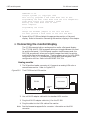
1
O C T A G O N
S Y S T E M S
Embedded PCs For Extreme Environments
PC-500 User’s Manual
5170 (0798)
DiskOnChip® is a registered trademark of M-Systems. Micro PC™, PC SmartLink™,
Octagon Systems Corporation®, the Octagon logo and the Micro PC logo are trademarks
of Octagon Systems Corporation. QuickBASIC® is a registered trademark of Microsoft
Corporation. QNX® is a registered trademark of QNX Software Systems Ltd.
ROM-DOS™ is a trademark of Datalight. Windows™ and Windows NT™ are trademarks of Microsoft Corporation. PICO FA™ is a trademark of Phoenix Technologies
Ltd.
Manual written by Susan Kendall.
Copyright 1997, 1998—Octagon Systems Corporation. All rights reserved. However,
any part of this document may be reproduced, provided that Octagon Systems Corporation is cited as the source. The contents of this manual and the specifications herein
may change without notice.
The information contained in this manual is believed to be correct. However, Octagon
assumes no responsibility for any of the circuits described herein, conveys no license
under any patent or other right, and makes no representations that the circuits are free
from patent infringement. Octagon makes no representation or warranty that such
applications will be suitable for the use specified without further testing or modification.
Octagon Systems Corporation general policy does not recommend the use of its products
in life support applications where the failure or malfunction of a component may directly
threaten life or injury. It is a Condition of Sale that the user of Octagon products in life
support applications assumes all the risk of such use and indemnifies Octagon against
all damage.
R
6510 W. 91st Ave.
Westminster, CO 80030
Technical support: 303-426-4521
Telephone: 303-430-1500
FAX: 303-426-8126
Web site: www.octagonsystems.com
PC-500 user’s manual
Notice to user
IMPORTANT!
Please read the following section before installing your product:
Octagon’s products are designed to be high in performance while consuming
very little power. In order to maintain this advantage, CMOS circuitry is
used.
CMOS chips have specific needs and some special requirements that the user
must be aware of. Read the following to help avoid damage to your card from
the use of CMOS chips.
≡ Using CMOS circuitry in industrial control
Industrial computers originally used LSTTL circuits. Because many PC
components are used in laptop computers, IC manufacturers are exclusively using CMOS technology. Both TTL and CMOS have failure
mechanisms, but they are different. Described below are some of the
failures which are common to all manufacturers of CMOS equipment.
However, much of the information has been put in the context of the
Micro PC.
Octagon has developed a reliable database of customer-induced, field
failures. The average MTBF of Micro PC cards exceeds 11 years, yet
there are failures. Most failures have been identified as customerinduced, but there is a small percentage that cannot be identified. As
expected, virtually all the failures occur when bringing up the first
system. On subsequent systems, the failure rate drops dramatically.
n Approximately 20% of the returned cards are problem-free. These
cards, typically, have the wrong jumper settings or the customer has
problems with the software. This causes frustration for the customer and incurs a testing charge from Octagon.
n Of the remaining 80% of the cards, 90% of these cards fail due to
customer misuse and accident. Customers often cannot pinpoint the
cause of the misuse.
n Therefore, 72% of the returned cards are damaged through some
type of misuse. Of the remaining 8%, Octagon is unable to determine the cause of the failure and repairs these cards at no charge if
they are under warranty.
Notice to user
PC-500 user’s manual
The most common failures on CPU cards are over voltage of the power
supply, static discharge, and damage to the serial and parallel ports.
On expansion cards, the most common failures are static discharge, over
voltage of inputs, over current of outputs, and misuse of the CMOS
circuitry with regards to power supply sequencing. In the case of the
video cards, the most common failure is to miswire the card to the flat
panel display. Miswiring can damage both the card and an expensive
display.
n Multiple component failures - The chance of a random component failure is very rare since the average MTBF of an Octagon card
is greater than 11 years. In a 7 year study, Octagon has never
found a single case where multiple IC failures were not caused by
misuse or accident. It is very probable that multiple component
failures indicate that they were user-induced.
n Testing “dead” cards - For a card that is “completely nonfunctional”, there is a simple test to determine accidental over voltage,
reverse voltage or other “forced” current situations. Unplug the card
from the bus and remove all cables. Using an ordinary digital
ohmmeter on the 2,000 ohm scale, measure the resistance between
power and ground. Record this number. Reverse the ohmmeter
leads and measure the resistance again. If the ratio of the resistances is 2:1 or greater, fault conditions most likely have occurred.
A common cause is miswiring the power supply.
n Improper power causes catastrophic failure - If a card has had
reverse polarity or high voltage applied, replacing a failed component is not an adequate fix. Other components probably have been
partially damaged or a failure mechanism has been induced. Therefore, a failure will probably occur in the future. For such cards,
Octagon highly recommends that these cards be replaced.
n Other over-voltage symptoms - In over-voltage situations, the
programmable logic devices, EPROMs and CPU chips, usually fail in
this order. The failed device may be hot to the touch. It is usually
the case that only one IC will be overheated at a time.
n Power sequencing - The major failure of I/O chips is caused by the
external application of input voltage while the Micro PC power is off.
If you apply 5V to the input of a TTL chip with the power off, nothing will happen. Applying a 5V input to a CMOS card will cause the
current to flow through the input and out the 5V power pin. This
current attempts to power up the card. Most inputs are rated at
25 mA maximum. When this is exceeded, the chip may be damaged.
n Failure on powerup - Even when there is not enough current to
destroy an input described above, the chip may be destroyed when
the power to the card is applied. This is due to the fact that the
input current biases the IC so that it acts as a forward biased diode
on powerup. This type of failure is typical on serial interface chips.
PC-500 user’s manual
Notice to user
n Hot insertion - Plugging cards into the card cage with the power on
will usually not cause a problem. (Octagon urges that you do not
do this!) However, the card may be damaged if the right sequence
of pins contacts as the card is pushed into the socket. This usually
damages bus driver chips and they may become hot when the power
is applied. This is one of the most common failures of expansion
cards.
n Terminated backplanes - Some customers try to use Micro PC
cards in backplanes that have resistor/capacitor termination networks. CMOS cards cannot be used with termination networks.
Generally, the cards will function erratically or the bus drivers may
fail due to excessive output currents.
n Excessive signal lead lengths - Another source of failure that was
identified years ago at Octagon was excessive lead lengths on digital
inputs. Long leads act as an antenna to pick up noise. They can
also act as unterminated transmission lines. When 5V is switch
onto a line, it creates a transient waveform. Octagon has seen
submicrosecond pulses of 8V or more. The solution is to place a
capacitor, for example 0.1 µF, across the switch contact. This will
also eliminate radio frequency and other high frequency pickup.
≡ Avoiding damage to the heatsink/CPU
WARNING!
When handling any Octagon CPU card, extreme care must be
taken not to strike the heatsink against another object, such
as a table edge. Also, be careful not to drop the CPU card,
since this may cause damage to the heatsink/CPU as well.
Epoxy adhesive bonds the heatsink to the CPU chip. When
the heatsink is struck, the epoxy adhesive does not allow the
heatsink to separate from the chip. The force of the blow to
the heatsink then causes the legs of the CPU chip to separate
from the PCB. This force damages both the CPU chip and
the PCB.
Note
Any physical damage to the CPU control card is not covered under
warranty.
Notice to user
PC-500 user’s manual
PC-500 user’s manual
Contents
Contents
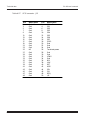
Abbreviations and terms used in this manual ........................................... xiii
Conventions used in this manual ................................................................... xv
About this manual
Overview: Section 1 – Installation
Chapter 1: Overview ......................................................................................... 1-1
Description .................................................................................................... 1-1
PC-500 major hardware features ................................................................. 1-1
CPU ....................................................................................................... 1-1
Up to 48 MB DRAM ............................................................................. 1-1
Solid-state disks ................................................................................... 1-2
Serial ports protected against ESD ..................................................... 1-3
Local bus SVGA, flat panel interface, and GUI accelerator .............. 1-3
Adjustable display bias supply ............................................................ 1-3
Industrial I/O using EZ I/O ................................................................. 1-4
Speaker, keyboard, and mouse ports ................................................... 1-4
PC/104 16-bit interface ........................................................................ 1-4
Ethernet ................................................................................................ 1-4
SCSI ...................................................................................................... 1-4
PC-500 major software features .................................................................. 1-5
Advanced power management and system management input ....... 1-5
Diagnostic software verifies system integrity automatically ............ 1-5
SETUP information stored in EEPROM for high reliability ............. 1-5
Phoenix BIOS ....................................................................................... 1-6
“Instant DOS” operating system ......................................................... 1-6
Programmable video BIOS .................................................................. 1-6
On-board flash file system ................................................................... 1-6
Octagon BIOS extensions .................................................................... 1-6
Interrupt routing: In system and programmable .............................. 1-6
Floppy and hard disk ports .................................................................. 1-6
Boot sequence ....................................................................................... 1-7
Multifunctional printer port ................................................................ 1-7
Watchdog timer added for safety ......................................................... 1-7
Real time calendar/clock with battery-backup ................................... 1-7
I/O connectors ....................................................................................... 1-7
Keypad and LCD display support for low cost operator interface .... 1-7
Hardware reset ..................................................................................... 1-8
5 Volt operation lowers system cost .................................................... 1-8
Rugged environmental operation ........................................................ 1-8
Size ........................................................................................................ 1-8
Chapter 2: Quick start ..................................................................................... 2-1
Installing the PC-500 ................................................................................... 2-1
Reference designators ................................................................................... 2-6
PC-500 power supply requirements ............................................................. 2-8
Running a demo program ............................................................................. 2-9
Logon message ..................................................................................... 2-9
What’s next .................................................................................................. 2-10
iii
Contents
PC-500 user’s manual
Chapter 3: SETUP programs .......................................................................... 3-1
Introduction ................................................................................................... 3-1
SETUP ........................................................................................................... 3-1
Running SETUP over the console port ............................................... 3-4
SETUP example ................................................................................... 3-8
SETSSD ......................................................................................................... 3-9
PMISETUP.................................................................................................... 3-9
SETIRQ.EXE ................................................................................................. 3-9
Chapter 4: Save and run programs ............................................................... 4-1
Save and run your programs on the PC-500 ............................................... 4-1
Saving programs and support files .............................................................. 4-1
Adding your application ....................................................................... 4-2
Autoexecuting your application ........................................................... 4-2
Overriding the autoexecution of your application .............................. 4-2
Overview: Section 2 – Hardware
Chapter 5: Serial ports ..................................................................................... 5-1
Description .................................................................................................... 5-1
Serial port options ......................................................................................... 5-1
Description of serial ports ............................................................................. 5-2
Conflicting COM port addresses ......................................................... 5-2
COM1 .................................................................................................... 5-2
COM2 .................................................................................................... 5-3
COM3 through COM5 interrupt/status port ...................................... 5-3
COM3 .................................................................................................... 5-5
COM4 .................................................................................................... 5-5
COM5 .................................................................................................... 5-6
Null modem cable ......................................................................................... 5-6
Mating receptacle ................................................................................. 5-6
Building your own cable ...................................................................... 5-7
Function and use of serial ports ................................................................... 5-9
COM1 as serial console device ............................................................. 5-9
COM1 through COM4 as RS-232 I/O ................................................. 5-9
COM5 as RS-485 transmitter control ................................................. 5-9
RS-485 network........................................................................................... 5-10
Chapter 6: LPT1 parallel port ........................................................................
LPT1 parallel port ........................................................................................
Printer ...........................................................................................................
Installing a printer ...............................................................................
Display ...........................................................................................................
Installing a display ..............................................................................
Keypad ...........................................................................................................
Installing a keypad ..............................................................................
Opto rack .......................................................................................................
6-1
6-1
6-1
6-1
6-2
6-2
6-2
6-2
6-3
Chapter 7: Console devices ............................................................................. 7-1
Description .................................................................................................... 7-1
Selecting console devices .............................................................................. 7-1
Local bus SVGA ................................................................................... 7-1
Serial console ........................................................................................ 7-1
Keyboard .............................................................................................. 7-3
iv
PC-500 user’s manual
Speaker .................................................................................................
Mouse ....................................................................................................
Enabling/disabling the video BIOS ..............................................................
Re-establishing communications when the console is not working ..
Contents
7-3
7-3
7-3
7-5
Chapter 8: SSDs, DRAM, and battery backup ............................................ 8-1
Description .................................................................................................... 8-1
SSD0 (optional) ............................................................................................. 8-1
Selecting SSD0 device type ................................................................. 8-1
SSD0 replaced with an SRAM device .......................................................... 8-1
SSD0 replaced with a flash device ............................................................... 8-2
Selecting an SSD BIOS ........................................................................ 8-2
SSD0 replaced with an EPROM/OTPROM ........................................ 8-3
SSD1 .............................................................................................................. 8-3
DRAM ............................................................................................................ 8-3
Battery backup for SSD0 SRAM and real time calendar clock .................. 8-4
Installing an AT battery ...................................................................... 8-4
Chapter 9: External drives ..............................................................................
Description ....................................................................................................
Floppy disk controller ...................................................................................
Power requirements .............................................................................
Installing a floppy disk drive ...............................................................
Hard disk controller ......................................................................................
Booting with ROM-DOS ...............................................................................
9-1
9-1
9-1
9-1
9-1
9-2
9-2
Chapter 10: IRQ routing and opto IRQs .................................................... 10-1
Interrupt routing ......................................................................................... 10-1
Opto IRQs .................................................................................................... 10-3
Interrupt routing matrix defaults .............................................................. 10-3
Programming .............................................................................................. 10-3
Master disable ............................................................................................. 10-4
Chapter 11: EZ I/O ........................................................................................... 11-1
Description .................................................................................................. 11-1
Pulling the I/O lines high or low ................................................................ 11-2
Organization of ports .................................................................................. 11-2
Port addressing .................................................................................. 11-3
Base I/O address ................................................................................ 11-3
Configuring and programming the EZ I/O ports ...................................... 11-4
Programming the EZ I/O ................................................................... 11-4
Configuring the EZ I/O ...................................................................... 11-4
Writing and reading from EZ I/O ...................................................... 11-5
EZ I/O output program examples ..................................................... 11-5
EZ I/O input program examples ........................................................ 11-6
Enhanced INT 17h function definitions .................................................... 11-6
Initialize EZ I/O ................................................................................. 11-6
Write EZ I/O ....................................................................................... 11-7
Read EZ I/O ........................................................................................ 11-8
Opto-module rack interface ........................................................................ 11-9
Interfacing to switches and other devices ............................................... 11-11
Chapter 12: LED signaling and “beep” codes ........................................... 12-1
Description .................................................................................................. 12-1
v
Contents
PC-500 user’s manual
Chapter 13: CRTs and flat panels ................................................................ 13-1
Description .................................................................................................. 13-1
Video features .............................................................................................. 13-1
Video options ............................................................................................... 13-1
Programming the video BIOS .................................................................... 13-2
Connecting the monitor/display ................................................................. 13-4
Analog monitor ................................................................................... 13-4
Flat panel display .............................................................................. 13-5
Flat panels requiring bias voltage .................................................... 13-5
LCD bias control examples ....................................................... 13-6
LCD bias control examples ....................................................... 13-7
Flat panel considerations ........................................................................... 13-7
Flat panel interface voltage select: W8 ............................................ 13-7
Inverted shift clock signal voltage level select: W9 ......................... 13-7
Chapter 14: PC/104 expansion ...................................................................... 14-1
Description .................................................................................................. 14-1
Chapter 15: SCSI ............................................................................................. 15-1
Description .................................................................................................. 15-1
Reprogramming the video BIOS ................................................................ 15-1
Chapter 16: Ethernet ...................................................................................... 16-1
Description .................................................................................................. 16-1
Overview: Section 3 – System management
Chapter 17: Watchdog timer and hardware reset ................................... 17-1
Description .................................................................................................. 17-1
Enhanced INT 17h function definitions .................................................... 17-1
Enable watchdog ................................................................................ 17-1
Strobe watchdog ................................................................................. 17-2
Disable watchdog ............................................................................... 17-2
Hardware reset ........................................................................................... 17-3
Chapter 18: Serial EEPROM and CMOS RAM .......................................... 18-1
Description .................................................................................................. 18-1
Enhanced INT 17h function definitions .................................................... 18-1
Serial EEPROM .......................................................................................... 18-1
Read a single word from the serial EEPROM .................................. 18-1
Write a single word to the serial EEPROM ...................................... 18-2
Read multiple words from the serial EEPROM ............................... 18-3
Write multiple words to the serial EEPROM ................................... 18-4
Return serial EEPROM size .............................................................. 18-4
CMOS RAM ................................................................................................. 18-5
Read extended CMOS RAM .............................................................. 18-5
Write extended CMOS RAM ............................................................. 18-6
Check CMOS battery ......................................................................... 18-7
Copy contents of serial EEPROM to extended CMOS RAM ........... 18-7
Copy contents of extended CMOS RAM to serial EEPROM ........... 18-8
Chapter 19: Transferring files/remote disks ............................................. 19-1
Transferring files between the PC-500 and your PC ................................ 19-1
Transferring files to the PC-500 ................................................................ 19-2
vi
PC-500 user’s manual
Contents
Transferring files from the PC-500 ............................................................ 19-2
Downloading files to the PC-500 using PC SmartLINK .......................... 19-3
Remote disks ............................................................................................... 19-5
Downloading files to the PC-500 using REMDISK/REMSERV ...... 19-5
PC-500 with one serial cable .................................................... 19-5
Chapter 20: Managing SSDs ......................................................................... 20-1
PICO FA flash file system .......................................................................... 20-1
Defining SSDs using SETSSD ................................................................... 20-1
Using PFORMAT to format an SSD .......................................................... 20-2
Formatting SSD1 ............................................................................... 20-2
Using SYS to make an SSD bootable ........................................................ 20-3
Adding operating system startup files (using SYS) ......................... 20-3
Changing boot SSD ..................................................................................... 20-4
Autoexecuting your application ......................................................... 20-4
Using SETSSD and TESTRFA to test an SSD ......................................... 20-4
Making copies of the PC-500 SSD ............................................................. 20-5
Programming copies of the PC-500 SSD ................................................... 20-5
Programming a new BIOS into SSD1 ....................................................... 20-6
Programming the video BIOS into an SSD ............................................... 20-6
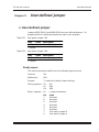
Chapter 21: User-defined jumper ................................................................ 21-1
User-defined jumper ................................................................................... 21-1
Read jumpers ...................................................................................... 21-1
Chapter 22: CPU power management ........................................................ 22-1
Description .................................................................................................. 22-1
Power management overview .................................................................... 22-1
Hardware controlled modes ........................................................................ 22-2
Device power management ........................................................................ 22-2
System power management ....................................................................... 22-3
How to initiate the SUSPEND/RESUME option ............................. 22-4
How to initiate the STANDBY option ............................................... 22-6
Save to disk ................................................................................................. 22-7
How to initiate the save to disk option ............................................. 22-8
Power management configuration ............................................................. 22-9
Enabling power management ........................................................... 22-9
System timers................................................................................... 22-10
Doze timer enable and resets .......................................................... 22-10
IDLE timer resets ............................................................................ 22-11
RESUME from STANDBY .............................................................. 22-12
RESUME from SUSPEND .............................................................. 22-13
Remote suspend/resume inputs ...................................................... 22-13
First Suspend/Resume Pulse: ................................................. 22-14
Second Suspend/Resume Pulse: ............................................. 22-14
External PMI interrupt ................................................................... 22-14
Thermal management ..................................................................... 22-15
Bitblt engine ..................................................................................... 22-15
PMISETUP ................................................................................................ 22-16
Chapter 23: Troubleshooting ........................................................................ 23-1
Technical assistance.................................................................................... 23-3
vii
Contents
PC-500 user’s manual
Overview: Section 4 – Appendices
Appendix A: Technical data ............................................................................ A-1
Technical specifications ................................................................................ A-1
Jumper settings ............................................................................................ A-6
Connector pinouts ......................................................................................... A-9
Tie wrap holes ............................................................................................. A-18
Appendix B: Software utilities ....................................................................... B-1
Introduction ................................................................................................... B-1
GETBIOS.EXE .............................................................................................. B-2
GETIMG.EXE ............................................................................................... B-2
GETIMGH.EXE ............................................................................................ B-3
HIMEM.SYS.................................................................................................. B-4
I17HNDLR.EXE ........................................................................................... B-5
LCDBIAS.EXE .............................................................................................. B-6
LPT1CON.COM ............................................................................................ B-7
PFORMAT.EXE ............................................................................................. B-7
PGMBIOS.EXE ............................................................................................. B-8
PGMIMG.EXE ............................................................................................... B-9
PGMIMGH.EXE ......................................................................................... B-10
PGMVIDEO.EXE ........................................................................................ B-11
PHDISK.EXE .............................................................................................. B-12
PICOFA.SYS ............................................................................................... B-13
PMISETUP.EXE ......................................................................................... B-14
REMDISK.EXE ........................................................................................... B-15
REMQUIT.COM .......................................................................................... B-17
REMSERV.EXE ........................................................................................... B-17
RESET.COM ................................................................................................ B-19
SCONSOLE.EXE ........................................................................................ B-19
SETIRQ.EXE ............................................................................................... B-20
SETSSD.EXE .............................................................................................. B-20
SETUP.COM ............................................................................................... B-22
TESTRFA.EXE ............................................................................................ B-23
TRANSFER.EXE ........................................................................................ B-24
VDISK.SYS ................................................................................................. B-26
Appendix C: Third party support ................................................................. C-1
Using QNX on the PC-500............................................................................ C-1
Programming QNX into SSD1 ............................................................ C-1
Using M-Systems DiskOnChip (DOC) ......................................................... C-1
Booting from the DOC drive ................................................................ C-2
Appendix D: Accessories .................................................................................D-1
Warranty
viii
PC-500 user’s manual
Contents
List of figures
Figure 2-1
Figure 2-2
Figure 2-3
Figure 5-1
Figure 5-2
Figure 5-3
Figure 5-4
Figure 6-1
Figure 6-2
Figure 6-3
Figure 7-1
Figure 7-2
Figure 7-3
Figure 10-1
Figure 11-1
Figure 11-2
Figure 11-3
Figure 11-4
Figure 13-1
Figure 13-2
Figure 13-3
Figure 14-1
Figure 19-1
Figure B-1
PC-500 component diagram ................................................. 2-2
PC-500 center-to-center hole dimensions ............................. 2-3
Power connector: P8, P9 ....................................................... 2-4
Null modem adapter and VTC-20F cable ............................ 5-7
Custom null modem cable for the PC-500 ........................... 5-8
PC-500 serial devices ............................................................ 5-9
RS-485 two-wire (half duplex) transmission ..................... 5-11
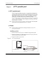
LPT1 as a printer port .......................................................... 6-1
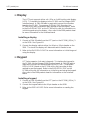
LPT1 as a display or keypad port ........................................ 6-3
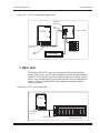
LPT1 and an opto rack .......................................................... 6-3
The PC-500 and a serial console .......................................... 7-2
VTC-20F cable and null modem adapter ............................. 7-2
Changing ROM Enable flowchart ........................................ 7-4
Interrupt routing matrix ..................................................... 10-2
Typical EZ I/O configurations ............................................. 11-1
Organization of ports .......................................................... 11-3
MPB-16PC opto rack hookup .............................................. 11-9
PC-500 interfacing with an STB-26 terminal board ....... 11-11
The PC-500, a VGA monitor, and an AT/PS-2 compatible
keyboard .............................................................................. 13-3
The PC-500 and a VGA monitor ......................................... 13-4
The PC-500 and a flat panel display .................................. 13-5
Typical PC/104 module stack ............................................. 14-1
Downloading files using TRANSFER.EXE ........................ 19-4
Cabling diagram for a standard cable ................................ B-16
ix
Contents
PC-500 user’s manual
List of tables
Table
Table
Table
Table
Table
Table
Table
Table
Table
Table
Table
Table
Table
Table
Table
Table
Table
Table
Table
Table
Table
2-1
2-2
2-3
2-4
2-5
2-6
2-7
2-8
3-1
5-1
5-2
5-3
5-4
5-5
5-6
5-7
5-8
5-9
5-10
5-11
5-12
Table 5-13
Table
Table
Table
Table
5-14
5-15
5-16
7-1
Table
Table
Table
Table
Table
8-1
8-2
8-3
8-4
10-1
Table
Table
Table
Table
Table
Table
Table
Table
Table
11-1
11-2
11-3
11-4
11-5
11-6
12-1
12-2
13-1
Table 13-2
Table 13-3
Table 16-1
Table 22-1
Table 22-2
Table A-1
x
Power connector: P8, P9 ....................................................... 2-5
PC-500 connectors ................................................................. 2-6
TTL and RS-485 interface: W1 ............................................ 2-6
RS-485 termination select jumper: W1 ............................... 2-6
BIOS and boot option jumper: W2 ....................................... 2-7
EZ I/O pull-up/pull-down, user option jumper: W3 ............ 2-7
Auxiliary option jumper: W4 ................................................ 2-7
SSD0 device configuration: W5, W2[7-8] ............................. 2-8
PC-500 SETUP parameters .................................................. 3-2
COM port options .................................................................. 5-1
Conflicting COM port addresses ........................................... 5-2
COM1 available addresses (IRQ 4 dedicated) ..................... 5-3
COM2 available addresses (IRQ3 dedicated) ...................... 5-3
Register 0A9h ........................................................................ 5-4
Reading the interrupt status port: Register 0A9h ............. 5-4
Interrupt status port (138h, 158h, 338h*, and 358h) ......... 5-5
COM3 available address and IRQ routing .......................... 5-5
COM4 available address and IRQ routing .......................... 5-5
Available addresses for COM5 (IRQ 5 default, routable) ... 5-6
COM5: J17, RS-485 or TTL interface ................................... 5-6
Custom RS-232 null modem cable for the PC-500:
First COM port ...................................................................... 5-7
Custom RS-232 null modem cable for the PC-500:
Second COM port................................................................... 5-8
RS-485 transmitter control: COM5 at location 320h ....... 5-10
RS-485 termination select jumper: W1 ............................. 5-10
RS-485 and TTL interfaces ................................................. 5-10
Video BIOS disabling and enabling options in SETUP
(C0000h-C7FFFh, C8000h-CFFFFh ROM Enable) ............ 7-4
SSD0 device selection jumpers: W5, W2[7-8] ....................... 8-1
Selecting an SSD BIOS: W2[5-6] ......................................... 8-2
SSD0 device configuration: W5, W2[7-8] ............................. 8-4
Battery connector: J8 ........................................................... 8-4
Interrupt status port (ISP) map setting
at I/O location 0A9h ............................................................ 10-4
EZ I/O connector: J11 ......................................................... 11-2
EZ I/O pull-up/pull-down jumpers: W3 ............................. 11-2
EZ I/O port address ............................................................. 11-3
Reading the EZ I/O port ...................................................... 11-4
EZ I/O port byte ................................................................... 11-5
EZ I/O opto-rack interface ................................................ 11-10
Ethernet LEDs .................................................................... 12-1
Additional error codes for Phoenix BIOS ........................... 12-4
Video controller and associated CRT, flat panel,
and PC-video circuitry ......................................................... 13-2
Flat panel interface voltage select: W8 ............................. 13-7
Inverted shift clock signal voltage level select: W9 .......... 13-8
Ethernet LEDs .................................................................... 16-1
Remote suspend/resume: J10 .......................................... 22-14
Enhanced mode, CPU clock speed: W2[3-4] .................... 22-16
PC-500 memory map ............................................................. A-3
PC-500 user’s manual
Table A-2
Table A-3
Table A-4
Table A-5
Table A-6
Table A-7
Table A-8
Table A-9
Table A-10
Table A-11
Table A-12
Table A-13
Table A-14
Table A-15
Table A-16
Table A-17
Table A-18
Table A-19
Table A-20
Table A-21
Table A-22
Table A-23
Table A-24
Table A-25
Table A-26
Table A-27
Table A-28
Table A-29
Table A-30
Table A-31
Table A-32
Table A-33
Table A-34
Table D-1
Table D-2
Table D-3
Table D-4
Table D-5
Table D-6
Contents
PC-500 I/O map ..................................................................... A-4
I/O map (Latched registered outputs via OctaGlue:
Address at X0A8h) ................................................................ A-5
I/O map (Configuration inputs via OctaGlue:
Address at X0A9h) ................................................................ A-5
COM1 available addresses ................................................... A-5
COM2 available addresses ................................................... A-6
Available LPT1 port addresses ............................................. A-6
TTL and RS-485 interface: W1 ............................................ A-6
RS-485 termination select jumper: W1 ............................... A-6
BIOS and boot option jumper: W2 ....................................... A-7
EZ I/O pull-up/pull-down, user option jumper: W3 ............ A-7
Auxiliary option jumper: W4 ................................................ A-7
SSD0 device configuration: W5 ............................................ A-8
Flat panel voltage select: W8 ............................................... A-8
Inverted shift clock signal voltage level select: W9 ............ A-8
PC/104 signal assignments: J1 ............................................ A-9
Keyboard connector: J2 ...................................................... A-10
Mouse connector: J3 ........................................................... A-10
Speaker connector: J4 ........................................................ A-10
Flat panel connector: J5 ..................................................... A-11
VGA connector: J6 .............................................................. A-11
PC video connector: J7 ....................................................... A-12
Battery connector: J8 ......................................................... A-12
Ethernet connector: J9 ....................................................... A-13
OPTOA and OPTOB: J10 .................................................. A-13
EZ I/O connector: J11 ......................................................... A-13
SCSI connector: J12 ........................................................... A-14
AT and industrial serial for COM1 and COM2: J13 ........ A-15
AT and industrial serial for COM3 and COM4: J14 ........ A-15
Floppy drive connector: J15 ............................................... A-16
LPT1 as printer connector: J16 ......................................... A-16
RS-485 and TTL interfaces for COM5: J17 ...................... A-17
IDE hard rive connector: J18 ............................................. A-17
Power connector: P8, P9 ..................................................... A-18
PC-500 mating connectors .................................................... D-1
Cables and terminal board ................................................... D-2
Memory devices ..................................................................... D-2
LCD displays and keypads ................................................... D-3
Opto rack and modules ......................................................... D-3
Miscellaneous part numbers ................................................. D-3
xi
Contents
xii
PC-500 user’s manual
PC-500 user’s manual
Abbreviations and terms used in this manual
Abbreviations and terms used in
this manual
Throughout this manual, the following symbols and terms are used:
Autoexecution
Automatic execution of a program on powerup or
reset.
BIOS
Basic Input Output System. Detailed instructions
that activate peripheral devices. See ROM-DOS.
BIOS drive
The solid-state disk which contains the system BIOS
and ROM-DOS.
bpp
bits per pixel
Console port
Video card or COM1 where BIOS and DOS messages
appear and keyboard input is available.
DRAM
Dynamic Random Access Memory devices. DRAMs
provide volatile memory with unlimited read and
write cycles.
Expansion card
The expansion cards add I/O functions to the Micro
PC system, such as analog input/output, digital
input/output, motion control, and display.
EZ I/O
This digital I/O chip supplies 24 I/O lines which can
be individually programmed as 5V input or 5V
output.
Flash
Electrically erasable PROM which allows at least
100,000 write cycles.
h
The suffix “h” denotes a hexadecimal number. A
decimal number has no prefix or suffix. For example, 1000h and 4096 are equivalent.
KB
Kilobyte (1,024 8-bit bytes).
MB
Megabyte (1,048,576 8-bit bytes).
Memory device
The type of static RAM, DRAM, flash memory, or
EPROM specified for either volatile or nonvolatile
memory.
PC/104
expansion
An expansion bus used for holding 8- and 16-bit
expansion cards.
PC SmartLINK
A serial communications software package designed
by Octagon for use with the PC-500 single board
computer. Refers to all versions of PC SmartLINK.
xiii
Abbreviations and terms used in this manual
xiv
PC-500 user’s manual
PC Video
A feature on the PC-500 which imports an external
video source into the virtual graphics array (VGA)
system. This feature allows for advanced video
connections including video overlays.
PICO FA
Phoenix’s flash file system used to access SSDs from
DOS as a read/write DOS drive.
ROM
Read Only Memory devices. ROMs provide nonvolatile memory, have a limited number of write cycles,
and include EPROMs and EEPROMs.
ROM-DOS
Operating system included in Micro PC ROM.
Single board
computer
A printed circuit board that contains a complete
computer: CPU, memory, I/O, and clock. The single
board computer controls the operation of all the
expansion cards.
Solid-state disk
(SSD)
A simulated disk which uses a high speed solid-state
memory device. For example, flash memory,
EEPROM, or static RAM.
Static RAM
Static Random Access Memory device. Static RAMs
provide volatile memory with unlimited read and
write cycles. They may be used with a backup
battery.
TTL compatible
Transistor transistor logic compatible; 0-5V logic
levels.
Virtual drive
A disk created in DOS or extended memory which
emulates an actual disk. The virtual drive provides
temporary storage for files. When power to the
computer is turned off the virtual drive disappears.
W[ - ]
Denotes a jumper block and the pins to connect.
XMODEM
A communications protocol which allows transfer of
files between two computers.
XON/XOFF
A communications protocol for asynchronous connections. The receiver can pace the sender by sending
the XOFF and XON characters to stop and continue
the data flow.
+5V Safe
+5V at the I/O connectors that is protected by a
0.75A fuse.
PC-500 user’s manual
Conventions used in this manual
Conventions used in this manual
This section explains the format used for notes, warnings, and command
entry.
≡ Notes and warnings
Special notes and warnings appear in this manual. Each one has a
different meaning and format. They are as follows:
Note
A note is supplementary or background information. At other times, it
is a hint or reminder that makes a task easier or quicker.
WARNING!
A warning gives vital information. Failure to heed a warning may cause system failure, equipment damage, or bodily
harm to the system operator.
≡ Command format and procedures
For some commands, you will only enter a single keyword (for example,
reset). For most commands, however, you will enter several keywords
followed by one or more parameters for which you must supply values.
Commands must be entered in a specific format. To indicate the format,
this manual uses a series of conventions that are explained below. The
conventions cover the rules for issuing all commands, including the most
complex ones. Most commands, however, are much simpler.
The command format looks like this:
command [type_this | or_ this] input {optional_input}
Follow these rules and conventions:
n Information which appears on your screen is shown in a different
type face, for example:
PhoenixBIOS(TM) A486 Version 1.03
Copyright (C) 1985-1994 Phoenix Technologies, Ltd.
All Rights Reserved
Octagon Systems Corp. PC500 CPU
n Commands that you must key in are shown in Courier Bold, for
example:
C:> RESET
xv
Conventions used in this manual
PC-500 user’s manual
n Italicized refers to information that is specific to your particular
system or program, e.g.,
Enter filename means enter the name of your file.
n Paired angle brackets are used to indicate a specific key on your
keyboard, e.g., <ESC> means the escape key; <CTRL> means the
control key; <F1> means the F1 function key.
n All addresses are given in hexadecimal, for example, 328h.
xvi
PC-500 user’s manual
About this manual
About this manual
The PC-500 user’s manual provides information about installing and
configuring the PC-500. This manual is divided into four sections:
n Section 1 – Installation
Chapter 1:
Overview
Chapter 2:
Quick start
Chapter 3:
SETUP programs
Chapter 4:
Save and run programs
n Section 2 – Hardware
Chapter 5:
Serial ports
Chapter 6:
LPT1 parallel port
Chapter 7:
Console devices
Chapter 8:
SSDs, DRAM, and battery backup
Chapter 9:
External drives
Chapter 10:
IRQ routing and opto IRQs
Chapter 11:
EZ I/O
Chapter 12:
LED signaling and “beep” codes
Chapter 13:
CRTs and flat panels
Chapter 14:
PC/104 expansion
Chapter 15:
SCSI
Chapter 16:
Ethernet
n Section 3 – System management
Chapter 17:
Watchdog timer and hardware reset
Chapter 18:
Serial EEPROM and CMOS RAM
Chapter 19:
Transferring files/remote disks
Chapter 20:
Managing SSDs
Chapter 21:
User-defined jumper
Chapter 22:
CPU power management
Chapter 23:
Troubleshooting
n Section 4 – Appendices
Appendix A:
Technical data
Appendix B:
Software utilities
Appendix C:
Third party support
Appendix D:
Accessories
About this manual
PC-500 user’s manual
PC-500 user’s manual
Overview:
Overview of Section 1
Section 1 – Installation
Section 1 provides installation and programming instructions, startup
options, and system configuration program examples. The following
chapters are included:
Chapter 1:
Chapter 2:
Chapter 3:
Chapter 4:
Overview
Quick start
SETUP programs
Save and run programs
Overview of Section 1
PC-500 user’s manual
PC-500 user’s manual
Overview
Overview
Chapter 1:
≡ Description
The PC-500 Mobile Industrial Computer™ (MIC) is a high performance,
single board PC in Octagon’s semi-custom product line. The PC-500
integrates serial communication, industrial digital I/O, a floppy and
local bus hard disk port, a multifunctional parallel port, and a local bus
video which supports monitors and flat panels. This single board computer has an interrupt routing matrix, two solid-state disks, a PC/104
interface, a SCSI-2 interface host port, and a 10Base-T Ethernet port.
The PC-500 also supports various CPU types including 586/133 MHz
and can have up to 16 MB of on-board DRAM with an expansion of
48 MB by adding a 32 MB DIMM module. This board is supplied with
DOS 6.22 in ROM but will also execute other operating systems such as
Windows™, Windows NT™, and QNX®. Since the PC-500 uses the
same functional blocks as the Micro PC™, the circuitry has been fully
proven as reliable and the software is compatible with the software in
the Micro PC series.
Specified to your engineering needs, the PC-500 can be ordered as a
semi-custom board in OEM quantities. The stocked version of the
PC-500 is listed below with the standard and optional features. The
standard version can be used for system development and an optional
version of the PC-500 is usually application specific.
≡ PC-500 major hardware features
CPU
The high performance 586 CPU comes in two versions. One version is a
120MHz586 and the other is a 133MHz586. Both versions operate at
3.3V for low power consumption. The PC-500 has a local bus speed of
33 MHz and an ISA bus speed of 8.33 MHz.
Up to 48 MB DRAM
The standard unit is supplied with 1 MB of fast, EDO surface mount
DRAM. The use of EDO DRAM increases performance by 20% which, in
most cases, eliminates the need for an expensive L2 cache. The PC-500
can contain up to 16 MB of on-board DRAM. Up to 32 MB of additional
DRAM can be added through an optional DIMM module, which makes a
total of 48 MB DRAM. Two holes are on-board the PC-500 to secure the
DIMM module in high vibration environments. All surface mount
1-1
Overview
PC-500 user’s manual
DRAM and DIMM modules from Octagon meet the full PC-500 temperature range. Customers who need a 0° to 70°C range can install
commercially available DIMM modules onto the PC-500.
n
n
n
n
1 MB EDO surface mount
16 MB EDO surface mount
SO-DIMM socket installed
SO-DIMM socket not installed
standard
optional
standard
optional
Solid-state disks
SSD0
A 32-pin DIP socket accepts either a 5V flash, SRAM, or 512 KB/1 MB
EPROM. The socket exhibits high retention force and affords a gas
tight contact. SSD0 optionally contains the BIOS drive and ROM-DOS
6.22 in ROM. By default, the optional SSD0 contains a 192 KB backup
BIOS with a 320 KB or a 512 KB drive area. Flash file system software
is included which allows the SSDs to emulate hard disk operation.
SSD0 options include:
n SSD0 socket installed
standard
n SSD0 socket not installed
optional
n SSD0 socket/EPROM installed
optional
For information on changing the device type, refer to the W5 SSD0
table in the Quick start chapter. You can also install compatible
PROMs into SSD0 through the supplied utility programs found on the
PC-500 utility disk. You can format the flash while in the socket.
EPROM usage, however, requires off-card programming from either a
master flash or a master EPROM.
SSD0 also supports a battery back up voltage. The PC-500 is capable of
supplying a battery voltage to SSD0 with SRAM installed.
SSD1
SSD1 is used for storage of the applications program. A standard 2 MB
5V flash is soldered on-card. The flash programmer is built-in which
allows on-card programming of the device. The PC-500 includes flash
file system software, which permits the SSDs to emulate hard disk
operation. Automatic “wear leveling” ensures that no single section of a
chip will reach its life span (100,000 times), while other sections will
scarcely be used. A 1 MB device reserves 192 KB for BIOS and 832 KB
for a drive area, a 2 MB device reserves 192 KB for BIOS and 1856 KB
for a drive area.
n 2 MB EPROM
n 1 MB EPROM
n SSD1 not installed
1-2
standard
optional
optional
PC-500 user’s manual
Overview
Serial ports protected against ESD
The PC-500 can have either two or five serial ports. All five serial ports
are standard, while COM3 through COM5 can be optionally omitted
from the PC-500. COM1 through COM4 are RS-232 and have the full
8-wire PC signal or they can optionally have 4-wire industrial RS-232
serial port lines. The 4-wire industrial RS-232 lines support RxD, TxD,
RTS, CTS and the DTR pin with a 1K pull-up to 5V. The interface to
COM5 is 2-wire industrial RS-485 also configurable to 2-wire TTL.
COM1 through COM5 have the following specifications:
n IEC1000, level 3, ESD protection specification
— Contact discharge ±6 kV
— Air-gap discharge ±8 kV
n Backdrive protection
n 16C550 compatible
n Up to 115.2K baud
n 16 byte FIFO buffers
n RS-232 voltages generated on-card
n COM1 through COM5
standard
n Omission of COM3 through COM5
optional
Local bus SVGA, flat panel interface, and GUI accelerator
The video system on the PC-500 uses the advanced 65550 video chip
from Chips & Technologies. It supports CRT, LCD and EL displays
with resolutions to 1024 x 768 bpp. Displays from CGA through SVGA
are supported. The 65550 is also a graphics accelerator with real time
PC-video being supported. Since the video circuitry operates on the
local bus at the full processor speed, programs like Windows execute
very rapidly. The video section has 2 MB of video RAM for high resolution displays and simultaneous CRT and flat panel operation.
The PC-500 supports both 3.3V and 5V flat panel displays. It has a 12V
connector for powering the backlighting on the displays and a 3.3V at
100mA connector to power the newer generation displays that use 3.3V
logic.
n Local bus flat panel video present
n No local bus flat panel video present
standard
optional
Adjustable display bias supply
An on-board voltage converter eliminates the need for a separate bias
supply for the LCD contrast control. The on-board power converter is
factory configurable and can be made to be compatible with most LCD
displays. The standard default range for the power converter is from
+23V to +29V.
n + Bias voltage 23V to 29V
n – Bias voltage/other range
n No bias supply
standard
optional
optional
1-3
Overview
PC-500 user’s manual
Industrial I/O using EZ I/O
The PC-500 is supplied with 24 lines of industrial I/O, using the Octagon EZ I/O digital I/O chip. Each EZ I/O line is programmable as an
input or output. The lines are 5V compatible and can sink and source
15mA. The EZ I/O port can drive the Octagon MPB series opto-isolation
module (Opto 22, G4 style) racks directly, controlling AC and DC loads
to 240V at 3A.
Speaker, keyboard, and mouse ports
The speaker connector is PC compatible and is a standard feature. The
keyboard controller accepts an AT style keyboard and has a PS-2 type
connector. The keyboard port is standard. The mouse port is optional
and conforms to the PS-2 standard. Neither the keyboard nor the
mouse are required for operation.
n Mouse port included
n Mouse port not included
standard
optional
PC/104 16-bit interface
This interface is a standard feature on the PC-500 and accepts an 8- or
a 16-bit PC/104 expansion board. PC/104 expansion boards are available from several manufacturers. As many as three PC/104 expansion
boards may be stacked on the PC-500.
Ethernet
The PC-500 provides a 10Base-T Ethernet port, located at J9. This
interface is a standard feature on the PC-500 and supports the IEEE
802.3 Ethernet standard. The Ethernet controller IC chip provides the
following:
n 16-bit ISA interface
n 4 KB on chip buffer
n Integrated 10 Base-T transceiver interface
n Four LEDs for status and diagnostic purposes
The PC-500 Ethernet interface supports the 10Base-T physical interface. This port operates at 10 MHz and uses twisted-pair wiring cable,
which is built in a star configuration. The 10Base-T physical interface
terminates at the standard, 8-position RJ-45, latching phone jack and is
vertically accessed.
SCSI
The PC-500 has a SCSI-2 host interface, located at J12. This device is a
16-bit ISA bus compatible part and has a sustained data rate of 10 MB
per second in the fast SCSI-2 synchronous transfer mode. It also has
parity generation and checking, noise filters, a low power mode, and ISA
bus RAM buffers.
1-4
PC-500 user’s manual
n SCSI-2 host interface, included
n SCSI-2 host interface, not included
Overview
standard
optional
≡ PC-500 major software features
Advanced power management and system management
input
Power management can be used to reduce power consumption or to
freeze the state of the program on the occurrence of a power management interrupt. Power consumption can be reduced by more than 60%.
This reduces the heat load and extends the battery life in mobile applications. There are opto-isolated system management and suspend/
resume inputs with 4-6V ranges. A system management input (SMI)
will cause the PC-500 to save its current status. When the system is
signaled to restart, execution resumes at the point the system last
stopped. The following are functions in the advanced power management and SMI:
n Suspend/resume by SMI input and software — halts CPU
n Wake up through various interrupts including keyboard, SMI
and serial port
n Slow CPU by dividing clock
n Contextual save to disk.
Diagnostic software verifies system integrity automatically
The PC-500 has built-in diagnostic software that can be used to verify
on-card I/O and memory functions. On powerup, a series of tests is
performed. If a problem occurs, the failed test can be identified by the
color sequence on an on-board, bicolored LED. The test is performed
automatically every time the system is reset or powered up. Software,
test equipment, monitor, keyboard, disks, or test fixtures are not required for memory verification. See the LED signaling “beep” codes
chapter for a complete listing of tests and failures and their descriptions.
SETUP information stored in EEPROM for high reliability
Loss of SETUP data is serious in industrial applications. Most PCs
store SETUP information in battery-backed CMOS RAM. If the battery
fails or is replaced during routine maintenance, this information is lost.
Without a keyboard and monitor in embedded applications, time consuming re-initialization is required. The PC-500 stores the SETUP
information in EEPROM with 1,536 bytes available to the user. Software routines to use this available memory come with the PC-500.
1-5
Overview
PC-500 user’s manual
Phoenix BIOS
The PC-500 has a Phoenix AT BIOS with power management and
Octagon BIOS extensions. The AT BIOS supports up to four EIDE
drives.
“Instant DOS” operating system
Datalight ROM-DOS v6.22 operating system is in flash. This means
that this version is always present on powerup. The system boots and
operates the same way as a desktop PC. Since all software and hardware are included, the system is fully operational “out of the box.”
Programmable video BIOS
The flash contains a video BIOS, which controls the on-board SVGA
controller. To support other flat panels, you can reprogram a new video
BIOS. By default, the video BIOS supports a CRT and Sharp monochrome dual drive flat panel in simultaneous mode.
On-board flash file system
The Phoenix PICO FA flash file system controls the on-board SSDs,
which allows read/write DOS access to the flash/SRAM. SSD0 can also
use EPROM. For certain types of flash, the flash file system uses “wear
leveling” to spread the usage and maximize the lifetime of these devices.
Octagon BIOS extensions
On-board BIOS extensions allow easy access to digital I/O, serial
EEPROM, LCD bias control, watchdog timer functions, etc.
Interrupt routing: In system and programmable
Software is on-board the PC-500 to change the interrupt routing and
some other features. The software allows more flexible use of interrupts on the PC-500 and outboard systems such as PC/104 expansion
boards.
Floppy and hard disk ports
The floppy disk port supports two drives with either 720 KB or 1.44 MB
capacities. The floppy port is terminated with a 34-pin IDC connector.
The EIDE hard drive port is terminated with a 44-pin, 2 mm connector.
+5V is supplied to the hard drive through the EIDE connector and is
optionally supplied to the floppy drive through the IDC connector.
1-6
PC-500 user’s manual
Overview
Boot sequence
A PC-500 can be configured to boot from the on-card, solid-state disk, an
external floppy or hard disk.
Multifunctional printer port
The PC-500 incorporates the latest enhanced parallel port.
n
n
n
n
n
Unidirectional
Bidirectional
IEEE 1284, ECP and EPP modes
24 mA of drive current
Backdrive protection
The following represent applications in the multifunctional parallel port:
n
n
n
n
n
LPT1 for PC compatible printers
17 general purpose digital I/O lines
Up to a 4 x 4 matrix keypad
4-line alphanumeric display
MPB-16PC, 16-position opto-module rack.
Watchdog timer added for safety
The watchdog timer resets the system if the program stops unexpectedly. The watchdog is enabled, disabled and strobed under software
control. The time-out is 1.6 seconds (typical).
Real time calendar/clock with battery-backup
The real time clock is fully AT compatible and uses the standard DOS
calls. An optional off-card battery powers the real time clock when the
5 volt supply is removed. A connector is provided for the external battery. The real time clock also provides the user with 128 bytes of userdefined CMOS-RAM.
I/O connectors
With the exception of the mouse, keyboard, and IDE, all I/O connectors
can be latched to prevent connector movement during shock or high
vibration.
Keypad and LCD display support for low cost operator
interface
For embedded applications, the parallel printer port or the EZ I/O port
can interface with a 16-key matrix keypad and a 2- or 4-line LCD display. The PC-500 is supplied with software that provides keypad scanning and display operation. Supplied display and keypad drivers in C
support these devices.
1-7
Overview
PC-500 user’s manual
Hardware reset
A hardware reset can be done by any of the following methods:
n Issuing the RESET software command (using the watchdog
function)
n Depressing the reset switch
n Cycling power
n Configuring the opto channel for RESET.
A hardware reset ensures complete reset of the system and all attached
peripherals. An expired watchdog timer cycle also causes a hardware
reset to occur.
5 Volt operation lowers system cost
The PC-500 operates from a single 5V ±5% supply. Located across the
power supply, the 6.2V, 5W zener diode protects against reverse voltage
and limits over voltage. The power supply generates the RS-232 voltages
on-board. The locking power connector is a standard PC power header
connector.
n 5V ±5%, 1.0A to 2.0A (dependent upon processor, speed and I/O
devices), less than 500 mA in standby
n +12V, -12V and -5V supplied to PC/104 connector and display
connector, not required for PC-500 operation
n A standard PC power supply may be used. See the Power supply
requirements section in the Quick start chapter for more information
on power supply selection and criteria.
Rugged environmental operation
n Operating temperature
n
n
n
n
n
Note
Nonoperating temperature
Relative humidity
Altitude
Shock
Vibration
Forced air cooling is required above 45°C if power management is not
used.
Size
5.75" x 8.0" x 0.9375"
1-8
-40° to 70°C, operating with
adequate airflow
-55° to 90°C, nonoperating
5% to 95% noncondensing
-100 to 10,000 m
10g, 3 axis
3g, 3 axis
PC-500 user’s manual
Quick start
Quick start
Chapter 2:
This chapter covers the basics of setting up a PC-500 system and tells you:
n How to install and power on the PC-500 and run a demo program
n How to use a serial console instead of the on-board SVGA video.
Follow the mounting procedures for the PC-500. To establish a serial
console link, go to the Serial console section in the Console devices chapter.
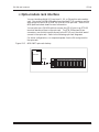
≡ Installing the PC-500
To install the PC-500 you will need the following equipment
(or equivalent):
n
n
n
n
n
PC-500 Mobile Industrial Computer
+5V power module
AT compatible keyboard with PS/2 connector
VGA monitor
VGA-12 cable
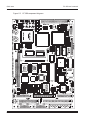
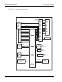
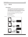
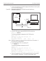
1. Refer to the PC-500 component diagram (Figure 2-1) for the location of
various connectors, before installing your PC-500 system.
WARNING!
The PC-500 Mobile Industrial Computer contains static sensitive CMOS components. Do the following to avoid damaging
your card and its components:
n Ground yourself before handling the PC-500 card
n Disconnect power before removing or inserting a PC/104
expansion board
n When programming a memory device, place the device in
the socket before applying power.
Hardware components required to mount the PC-500 (not included):
n 8 threaded hex stainless steel standoffs (4-40 x 3/8")
n 8 screws (4-40 x 1/4")
n 8 internal star lock washers (4-40)
2. Use the #4 standoffs, washers, and screws and place them in the eight
holes on the PC-500 board. Refer to Figure 2-2 for the center-to-center
mounting hole dimensions and for the location of the designated holes used
for mounting the hardware.
2-1
Quick start
Figure 2-1 PC-500 component diagram
2-2
PC-500 user’s manual
PC-500 user’s manual
Quick start
Figure 2-2 PC-500 center-to-center hole dimensions
2-3
Quick start
PC-500 user’s manual
WARNING!
Before the PC-500 is powered on for bench testing, all eight
standoffs, screws and washers should be secured to the
board. The standoff pieces will ensure full support of the
PC-500 not only on all four sides, but also in the middle of
the board. These hardware pieces will reduce the circuit
board flex when the PC/104 expansion board and/or the SSD0
are inserted. Flexing of the PC-500 board should be avoided,
since it can cause problems with the copper circuit traces
Figure 2-4 PC-500, keyboard, and monitor and the surface
mounted components.
3. The power supply connector is located at P8, P9. Make certain to connect the ground wires (typically black) to all ground connectors at P8,
P9 on the PC-500. Refer to Figure 2-3.
WARNING!
Accidently crossing the wires, i.e., plugging +5V wires into
the ground connector or the ground wires into the +5V connector will damage the PC-500.
Figure 2-3 Power connector: P8, P9
Note
2-4
NC
Orange
+5V
Red
+12V
Yellow
–12V
Gnd
Black
Blue
Gnd
Black
Gnd
–5V
White
Black
+5V
Red
Gnd
+5V
Black
+5V
Red
Standard cable wire colors
Red
P8, P9
Power header
By removing the keys on the PC-500, it is possible to key your power
connector header to your power supply connector. To insert the power
connector without removing the keys, angle the connector at 90° and
then place it on P8, P9.
PC-500 user’s manual
Table 2-1
Note
Quick start
Power connector: P8, P9
Pin Description (P8)
Pin Description (P9)
1
N.C.
1
Gnd
2
+5V
2
Gnd
3
+12V
3
–5V
4
5
–12V
Gnd
4
5
+5V
+5V
6
Gnd
6
+5V
See the Accessories appendix for mating information on the power
connector.
4. Connect the PS-2 style keyboard directly to the keyboard port at J2 and
a VGA monitor to J6 using a VGA-12 cable. Refer to Figure 2-4.
Keyboard
cable
Keyboard
connector, J2
Mouse
connector, J3
VGA Monitor
PC-500
J6
VGA-12
cable
2-5
Quick start
PC-500 user’s manual
≡ Reference designators
The following tables illustrate jumper connections and pins jumpered on
the PC-500:
Table 2-2
Note
Table 2-3
PC-500 connectors
Reference
designator
J1
Description
PC/104
Reference
designator
J11
Description
EZ I/O
J2
Keyboard
J12
SCSI
J3
Mouse
J13
COM1/COM2
J4
Speaker
J14
COM3/COM4
J5
Flat panel
J15
Floppy disk port
J6
SVGA CRT analog
J16
LPT1 printer
J7
PC video
J17
J8
J9
Battery
Ethernet
J18
P8, P9
COM5/RS-485 &
TTL interface
IDE hard drive
Power
J10
OPTOA/OPTOB
See the Accessories appendix for mating information on the above
connectors.
TTL and RS-485 interface: W1
Pins
Description
[2-4][5-6]
TTL interface
[1-2][3-5][4-6]*
RS-485 interface
* = default
Table 2-4
RS-485 termination select jumper: W1
Pins
[7-8]*
[9-10]*
[7-9]
[8-10]
Description
RS-485 terminated(-), idle line at mark
RS-485 terminated(+), idle line at mark
RS-485 terminated(-), idle line at space
RS-485 terminated(+), idle line at space
* = default
Note: For no termination, remove jumpers from pins 7, 8, 9, and 10.
2-6
PC-500 user’s manual
Table 2-5
Quick start
BIOS and boot option jumper: W2
Pins
[1–2]*
[5–6]*
Label Description
V0
C0000–C7FFF BIOS region toggle** (video BIOS
region 1)
E
Enhanced mode, CPU clock speed: on = 133 MHz;
off = 120 MHz
B
BIOS device: on = SSD1; off = SSD0
[7–8]*
T
SSD0 type: on = flash/SRAM; off = EPROM
[9–10]*
S
Use SETUP information: on = EEPROM; off = BIOS
default
[3–4]
* = default
** = Toggles in BIOS extension areas work in combination with toggles in the
SETUP BIOS extension areas. See the Console devices chapter for more
information on BIOS regions.
Table 2-6
EZ I/O pull-up/pull-down, user option jumper: W3
Pins
Label
Description
[1–2]*
Pull up to +5V
[2–4]
Pull down to Gnd
[9–10]*
UA
User option jumper A
* = default
Table 2-7
Auxiliary option jumper: W4
Pins
[1–2]*
[3–4]*
Label Description
V1
C8000–CFFFF BIOS region toggle** (video BIOS
region 2)
X
D8000–DFFFF BIOS region toggle*** (PICO FA)
[5–6]*
UB
User option jumper B
[7–8]*
VE
VGA controller: on = enabled; off = disabled
[9–10]
I
IRQ matrix: on = disabled; off = enabled
* = factory default
** = Toggles in BIOS extension areas work in combination with toggles in the
SETUP BIOS extension areas. See the Console devices chapter for more
information on BIOS regions.
*** = Enables or disables PICO Flash Array extended BIOS.
2-7
Quick start
PC-500 user’s manual
Table 2-8
SSD0 device configuration: W5, W2[7-8]
Pins
W5[1–3, 2–4, 5–7, 8–10] W2[7–8]
Description
SRAM with battery backup*
W5[1–2, 3–4, 5–6, 9–10] W2[7–8]
Flash
W5[1–2, 3–4, 5–6, 9–10]
EPROM**
* = default, pins jumpered
** = W2[7–8] is not jumpered
≡ PC-500 power supply requirements
The PC-500 is designed to operate from a single +5 VDC supply. An AT
compatible power supply connector header (P8, P9) is on board and
ensures the required number of power and ground paths from the power
supply. Make sure that you utilize all three +5 VDC conductors and all
four ground conductors.
The power connector at P8, P9 also provides +/-12 VDC and -5 VDC
required for any PC/104 expansion board. P8, P9 also supplies the
correct voltage, +12 VDC, for flat panels that require back light operation. Refer to the P8, P9 power connector Table 2-1 for a complete
listing of pinouts and their description.
The maximum current requirements for the PC-500 is 2.0 A provided
through P8, P9. It is important that a quality power supply be used
with the PC-500. For example, when a particular application calls for a
custom power supply, there are several internal issues to consider such
as current capacity, line and load regulation, maximum ripple, hold up
time, efficiency, and current limiting. The user should also consider the
power devices and equipment such as the power cable conductor gauge,
number and length of conductors, mating connectors, and the power
supply to external devices such as hard drives, floppy drives, displays,
mouse, and keyboard.
The proper selection of a quality power supply ensures reliability and
proper functioning of the PC-500.
WARNING!
Make sure the power supply is OFF when connecting the
power cable to the PC-500 board. Damage to the PC-500 may
occur if the power is ON when connecting the power cable.
2-8
PC-500 user’s manual
Quick start
≡ Running a demo program
Logon message
1. Power on the PC-500.
2. A logon message similar to the one below appears on your PC
monitor:
PhoenixBIOS(TM) A486 Version x.xx
Copyright (C) 1985-1994
Phoenix Technologies, Ltd.
All Rights Reserved
Octagon Systems Corp. PC500 CPU
PC500 BIOS vx.xx - mm/dd/yy
Am586-WB processor detected operating at 133 Mhz
640K Base Memory, 5x86 133 MHz
On board memory configured as EDO DRAM
INT 17h BIOS extension vx.xx
Copyright (c) 1995-96 Octagon Systems Corporation
PICO Flash Array
Copyright (c) 1996, Phoenix Technologies Ltd.
Resident Flash (RFA) OEM Layer
Phoenix Pico Flash Array
Octagon Systems vx.xx
First drive is in SSD1 (1856K, AMD 2 MB flash)
Starting ROM-DOS...
HIMEM v6.22 (Revision x.xx)
Copyright (c) 1989-1995 Phoenix, Inc.
VDISK v6.22 (Revision x.xx)
Copyright (c) 1989-1995 Datalight, Inc.
Extended Memory Present
VDISK v6.22 (Revision x.xx)
Copyright (c) 1989-1995 Datalight, Inc.
Formatting 2304K XMS memory as drive E:
PC500 C:\> demo
To begin the demo.exe program, press any key.
Then a demonstration program will begin. If you do not get the proper
logon message, please do the following:
n Make sure all jumpers are set to factory defaults. Refer to the
Technical data appendix for all default jumper settings.
2-9
Quick start
PC-500 user’s manual
n If the system still does not respond, remove W2[9-10] to run BIOS
default SETUP and try again. Also, refer to the Troubleshooting
chapter.
3. Use the directory command to make sure your equipment and software
are working properly. Enter:
PC500 C:\> DIR
A directory listing of files stored in the SSD1 socket should appear:
Volume in drive C is SSD1
Volume Serial Number is 3214-1BE4
Directory of C:\
COMMAND
AUTOEXEC
CONFIG
DOS
UTILS
DEMO.EXE
DEMO
COM
26,321
BAT
38
SYS
67
<DIR>
<DIR>
EXE
27,922
BAS
5,045
7 file(s)
04-12-96
6:22p
04-12-96
8:26p
04-12-96
8:26p
04-12-96
8:26p
04-12-96
8:26p
04-12-96
8:26p
04-12-96
8:26p
26,426 bytes
105,472 bytes free
≡ What’s next
1. To run SETUP and configure the system, see the SETUP programs
chapter.
2. To connect a floppy and/or hard drive, see the External drives chapter.
3. Refer to the Transferring files/remote disks chapter to transfer files
from a host PC and to use a remote disk via a serial connection.
4. To use a serial console, refer to the Console devices chapter.
2-10
PC-500 user’s manual
Chapter 3:
SETUP programs
SETUP programs
≡ Introduction
Three system configuration programs exist for the PC-500. They are:
n SETUP – Configures devices set up by the BIOS such as serial ports
and floppy drives
n SETSSD – Configures PICO FA SSD device order
n PMISETUP – Configures power management options at a more
detailed level than SETUP
n SETIRQ – Configures the interrupt routing matrix.
≡ SETUP
SETUP can be entered in one of two ways:
n Run SETUP.COM
n Press the “backspace” key followed by the “S” key during BIOS
POST sequence (this occurs between the memory test and boot).
Also, by removing the USESETUP jumper from W2[9-10], you may
force the setup to temporarily revert to the BIOS defaults (Table 3-1)
and also allow the user to reconfigure the setup options.
The SETUP program defines the PC-500 system parameters. This
program is shipped with default configuration parameters stored in
the serial EEPROM. Changes are made by running the SETUP
program. The SETUP program is stored on the SSD1 drive and on
the PC-500 utility disk.
3-1
SETUP programs
Table 3-1
PC-500 user’s manual
PC-500 SETUP parameters
SETUP parameters
Description
Default
Serial console on COM1
Allows COM1 to be used
as a console when
on-board video is disabled
Specifies communications
rate between PC and
PC-500 when serial console
is in use
Extensive memory testing
performed on bootup
Specifies whether the floppy
drive will be ignored as a
boot device
Specifies COM1
enable/disable
COM1 address
Specifies COM2
enable/disable
COM2 address
Specifies LPT port
enable/disable
Specifies mode to use
with parallel port
Specifies address to use
w/parallel port
Specifies number of
floppy drives attached
Specifies location of floppy:
on-board or on PC/104 bus
Specifies usage of
on-board IDE connector or
PC/104 bus
Enabled
COM1 console baud rate
Power-on memory test
Boot sequence
Serial port COM1
Serial port COM1 address
Serial port COM2
Serial port COM2 address
Parallel (LPT) port
Parallel port mode
Parallel port address
Number of floppy drives
On-board floppy
controller
On-board IDE interface
3-2
9600
Enabled
C: Only
Enabled
3F8h
Enabled
2F8h
Enabled
Bidirectional
printer port
378h
0
Disabled
Disabled
PC-500 user’s manual
Table 3-1
SETUP programs
PC-500 SETUP parameters (cont’d)
SETUP parameters
Primary master fixed
disk
Primary slave fixed
disk
Secondary master
fixed disk
Secondary slave fixed
disk
Internal CPU cache
CPU cache mode
Limit CPU to half
speed
SETUP entry via
hotkey
Power management
Doze clock
Time update after
suspend
DIMM module type
ROM Enable
C0000-C7FFFh
ROM Enable
C8000-CFFFFh
ROM Enable
D8000h-DFFFFh
Shadow
Shadow
C8000h-CFFFFh
Shadow
D0000h-D7FFFh
Shadow
D8000h-DFFFFh
Description
Specifies which IDE interface
is used
Specifies which IDE interface
is used
Specifies which IDE interface
is used
Specifies which IDE interface
is used
Specifies CPU cache
enable/disable
Specifies write-through/writeback on some CPUs (processor
specific)
Default
None
None
None
None
Enabled
Write-back
Limits the top CPU speed
No
Specifies <backspace><S> hotkey
enable/disable
Specifies power management
enable/disable
Specifies doze mode in power
management to slow or stop
the clock
To allow update of time after
suspend mode
Specifies the type of
DIMM module
Enabled
Toggles video BIOS region
(first 32 KB)
Toggles video BIOS, second
region (first 8 KB is video
BIOS)
Toggles extended BIOS area
for PICO FA and
INT 17h BIOS
Specifies video BIOS
shadow enable/disable
(first 32 KB)
Shadow enable/disable
(first 8 KB is video BIOS)
Enabled
Enabled
Slow
Enabled
EDO
Enabled
Enabled
Enabled
Enabled
Shadow enable/disable
Disabled
Shadow enable/disable
Disabled
3-3
SETUP programs
PC-500 user’s manual
Running SETUP over the console port
1. To run SETUP make sure you have established a communications link
between a keyboard and monitor with the PC-500 or a serial communications link between the PC-500 and your PC. See the Console devices
chapter for more information on these two communication links.
2. Enter:
PC500 C:\> SETUP
Note
If you are not booting from the SSD0 drive, the drive designator may
differ.
Note
You may also enter SETUP after the memory test and before the system has booted by pressing the “backspace” key followed by the “S” key.
3. The system will display the PC-500 setup parameters and available
options. Select the option by pressing the space bar until the correct
information appears, then press <ENTER>. Press <ESC> twice if you
want to exit SETUP without saving your responses.
Note
Options having an * are default settings.
n
Serial Console on COM1:
ENABLED*
DISABLED
WARNING!
Disabling the serial console when there is no video monitor
present will stop further serial console communication with
the system after the system resets. Once disabled, you may
re-enable the serial console by running SETUP. To run
SETUP, do one of the following steps:
n Remove the USESETUP jumper, reboot and run SETUP
n Install a video monitor, reboot and run SETUP. You
have elected to DISABLE the serial console.
n
3-4
Serial Port COM1 Console Baud Rate:
1200
2400
4800
9600*
14400
19200
28800
38400
57600
115200
PC-500 user’s manual
n
SETUP programs
Power on memory test:
Enabled*
Disabled
You may want to disable the memory test to speed up the boot process.
You may also press the space bar to cancel the memory test while in
progress.
n
Boot Sequence:
C: Only*
A: Then C:
n
Serial Port COM1:
Enabled*
Disabled
n
Serial Port COM1 address:
3F8h*
2F8h
338h
3E8h
2E8h
220h
238h
2E0h
228h
n
Serial Port COM2:
Enabled*
Disabled
n
Serial Port COM2 address:
2F8h*
338h
3E8h
2E8h
220h
238h
2E8h
2E0h
228h
Note
Octagon strongly recommends the use of 3F8h for COM1 and 2F8h for
COM2.
Note
The choices for COM1 and COM2 addresses are mutually exclusive;
therefore, you may not see all the choices listed above. COM1 and
COM2 addresses may also conflict with those belonging to COM3
through COM5. Refer to the Serial ports chapter for a complete description on conflicting addresses.
n
Parallel (LPT) Port:
Enabled*
Disabled
3-5
SETUP programs
PC-500 user’s manual
n
Parallel Port Mode:
Bidirectional mode*
EPP mode
ECP mode
Standard (Unidirectional) mode
n
Parallel Port Address:
378h*
278h
3BCh
n
Note
3-6
IRQ for LPT port
IRQ7*
IRQ5
Standard mode is provided for compatibility only. We recommend the
use of bidirectional mode. EPP and ECP modes are provided for equipment that has the capability to operate in these modes for enhanced
performance.
n
Number of floppy drives:
0*, 1, 2
n
Onboard floppy controller:
Enabled (enables onboard floppy connector, J15)
Disabled*
n
Drives A and B:
No* - requires a swap in the cable
Yes - does not require a swap in the cable
n
Floppy drive 1 size:
Not Installed
5.25", 360 KB
5.25", 1.2 MB
3.5", 720 KB
3.5", 1.44 MB*
n
Floppy drive 2 size:
Not Installed
5.25", 360K
5.25", 1.2 MB
3.5", 720KB
3.5", 1.44 MB*
n
Onboard IDE interface:
Disabled*
Enabled (enables J18)
PC-500 user’s manual
SETUP programs
n
Primary master fixed disk:
None*
Auto - detects hard disk parameters
User - detects hard disk parameters
n
Drive 1 parameters:
Cylinders (xxx)
Heads (xx)
Sectors (xx)
n
Internal CPU cache:
Enabled*
Disabled
n
Limit CPU to half speed:
NO*
YES
n
Setup entry via hotkey:
Enabled*
Disabled
n
Power management:
Enabled*
Disabled
n
Doze clock:
Slow*
Stop
n
Time update after suspend:
Enabled*
Disabled
n
DIMM module type:
EDO*
Standard
n
Shadow C0000h - C7FFFh:
Disabled
Enabled*
n
Shadow C8000h - CFFFFh:
Disabled
Enabled*
n
Shadow D0000h - D7FFFh:
Disabled*
Enabled
3-7
SETUP programs
PC-500 user’s manual
n
Shadow D8000h - DFFFFh:
Disabled*
Enabled
Press ENTER to SAVE the changes or
Press ESC to EXIT without saving the changes.
Saving options.
Options saved.
Depending on the options you have selected, the system may display the
following message:
You must reset for these options to take effect.
If you entered SETUP with the hotkeys (i.e., “backspace” and “S” keys),
the system will reboot automatically.
SETUP example
The following example configures a system with no memory test, 9600
baud, printer at 378h, and booting from C:
OCTAGON SYSTEMS CORPORATION
PC-500 SETUP UTILITY Vx.x
(c) Phoenix Technologies, Ltd. 1985, 1995
_________________________________________________
(Press SPACE to CHANGE, ENTER to ACCEPT, ESC to EXIT)
Serial Console on COM1:
COM1 Console Baud Rate:
Power on memory test:
Boot Sequence:
Serial Port COM1:
Serial Port COM1 Address:
Serial Port COM2:
Serial Port COM2 Address:
Parallel (LPT) Port:
Parallel Port Mode:
Parallel Port Address:
Number of floppy drives:
Onboard Floppy Controller:
Swap drives A and B:
Floppy drive 1 size:
Onboard IDE Interface:
Primary Master Fixed Disk:
Primary Slave Fixed Disk:
Secondary Master Fixed Disk:
Secondary Slave Fixed Disk:
Internal CPU cache:
Limit CPU to half speed:
SETUP Entry via Hotkey:
Power Management:
Doze Clock (slow, stop):
Time Update after Suspend:
DIMM Module Type:
Enable ROM at C0000h-C7FFFh:
Enable ROM at C8000h-CFFFFh:
Enable ROM at C8000h-DFFFFh:
3-8
ENABLED
9600
DISABLED
C: ONLY
ENABLED
3F8h (default)
ENABLED
2F8h (default)
ENABLED
Bidirectional Printer Port
378h
1
ENABLED
NO
3.5", 1.44 MB
ENABLED
AUTO
USER
NONE
NONE
ENABLED
NO
ENABLED
ENABLED
SLOW
ENABLED
EDO
ENABLED
ENABLED
ENABLED
PC-500 user’s manual
Shadow
Shadow
Shadow
Shadow
SETUP programs
D0000h-C7FFFh:
C8000h-CFFFFh:
D0000h-D7FFFh:
D8000h-DFFFFh:
ENABLED
ENABLED
DISABLED
DISABLED
Press ENTER to SAVE the changes
Press R to RESTART with original values or
Press ESC to EXIT without saving the changes:
Options Saved.
You must reset for these options to take effect.
PC500 C:\>
Note
Executing SETUP /D will change all setup parameters to default values.
≡ SETSSD
For more information on SETSSD, refer to the Defining SSDs using
SETSSD section in the Managing SSDs chapter.
≡ PMISETUP
PMISETUP allows the user to customize the power management features of the PC-500. Refer to the CPU power management chapter. See
also the Software utilities appendix for details.
≡ SETIRQ.EXE
To change interrupts via software using SETIRQ.EXE, refer to the
Programming section in the IRQ routing opto IRQs chapter.
3-9
SETUP programs
3-10
PC-500 user’s manual
PC-500 user’s manual
Chapter 4:
Save and run programs
Save and run programs
≡ Save and run your programs on the PC-500
Once you have written, tested and debugged your application, you can
then save it to flash memory in SSD1 or SSD0 (if flash or SRAM). When
you reboot the PC-500, your program can automatically load into DOS
memory and execute. As shipped from the factory, SSD1 already contains a bootable ROM-DOS.
This chapter describes the following:
n Saving an application program to SSD1
n Autoexecuting the program from the PC-500
n Overriding autoexecution of your program.
The information in this chapter assumes you are using ROM-DOS in
your application. Some Microsoft programs make undocumented DOS
calls. With ROM-DOS, an error returns when an undocumented DOS
call is made, causing your program to operate erratically. We recommend booting from SSD1, using your own DOS, when using programs
with undocumented DOS calls. Refer to the section Adding operating
system startup files in the Managing SSDs chapter for more information
on saving and autoexecuting programs.
≡ Saving programs and support files
By default, the drive in SSD1 comes preformatted from the factory,
loaded with ROM-DOS startup files and an example demo program. To
replace the demo program on SSD1 with your own, see the section
Adding your application, in this chapter. To reformat an SSD or to add
your own operating system, please refer to the Managing SSDs chapter.
WARNING!
Reformatting SSD1 requires the use of a floppy or a hard
disk to restore system files.
4-1
Save and run programs
PC-500 user’s manual
Adding your application
To add your application to your SSD, do the following:
1. Three methods of copying your application to the SSD are available. Do
one of the following:
n From a local drive to the PC-500, issue the COPY command.
n From a host drive, download your application by issuing the
TRANSFER command when using PC SmartLINK. Refer to the
section, Transferring files between the PC-500 and your PC in the
Transferring files/remote disks chapter.
n To establish a remote drive and copy from it, issue the REMDISK
and REMSERV commands. Refer to the section, Transferring files
between the PC-500 and your PC in the Transferring files/remote
disks chapter.
2. Add or remove any device drivers for your application. You may want to
do the same for the CONFIG.SYS file on SSD1. Remember to add these
drivers to your drive as well.
3. To autoexecute your application, add your application name to the
AUTOEXEC.BAT file. To replace our example program (DEMO.EXE)
with your application, substitute DEMO in the AUTOEXEC.BAT file
with your applications’ filename.
Autoexecuting your application
This section describes how to autoexecute your application.
1. To autoexecute your application in SSD1, use the SETSSD command to
define your SSD as the boot device. Since you need to define the order
of SSD1 as the first of the SSDs (and before any IDE drives), enter the
following command:
PC500 C:\> SETSSD SSD1 SSD0 /before
2. Reset the system. SSD1 is now drive C: and your application should
begin execution.
Note
If the SETUP option “Boot Sequence” is set to “A: THEN C:”, remove
any floppy in drive A: before resetting the system.
Note
We recommend that you leave SSD0 in the SETSSD options or that you
have a copy of SETSSD.EXE on SSD1. This allows you to change your
boot device back to SSD0 when needed.
Note
The SETSSD options are not used when W2[9-10] is not jumpered.
Overriding the autoexecution of your application
You may stop the autoexecution of your application by doing one of the
following options:
4-2
PC-500 user’s manual
Save and run programs
Option 1
1. Press F5 or F8 on your local keyboard. For more information, see
your ROM-DOS manual.
Option 2
1. Change AUTOEXEC.BAT and/or CONFIG.SYS to not call out your
program.
Option 3
1. Install a floppy.
2. Change SETUP option “Boot Sequence” to “A: THEN C:”
3. Change SETUP to enable the floppy.
4. Boot from floppy.
5. Change AUTOEXEC.BAT on C:.
4-3
Save and run programs
4-4
PC-500 user’s manual
PC-500 user’s manual
Overview:
Overview of Section 2
Section 2 – Hardware
Section 2 discusses usage, functions, and system configurations of the
PC-500’s major hardware features. The following chapters are
included:
Chapter 5:
Chapter 6:
Chapter 7:
Chapter 8:
Chapter 9:
Chapter 10:
Chapter 11:
Chapter 12:
Chapter 13:
Chapter 14:
Chapter 15:
Chapter 16:
Serial ports
LPT1 parallel port
Console devices
SSDs, DRAM, and battery backup
External drives
IRQ routing and opto IRQs
EZ I/O
LED signaling and “beep” codes
CRTs and flat panels
PC/104 expansion
SCSI
Ethernet
Overview of Section 2
PC-500 user’s manual
PC-500 user’s manual
Chapter 5:
Serial ports
Serial ports
≡ Description
The PC-500 has five standard serial ports, COM1 through COM5.
Under OEM contract, COM3 through COM5 can be omitted. These
serial ports interface to a printer, terminal, or other serial device. All
ports support 5-, 6-, 7-, or 8-bit word lengths, 1, 1.5, or 2 stop bits, and
baud rates up to 115.2K. All ports have the following specifications:
n 16C550 compatible
n 16 byte FIFO buffers
n IEC 1000, level 3, ESD protection
— Contact discharge ±6 kV
— Air-gap discharge ±8 kV
n Backdrive protection
n IDC connectors which have the standard IBM PC pinout
n Up to 115.2k Baud operation
≡ Serial port options
The standard version of the PC-500 has COM1 and COM2 installed as
an 8-wire interface. Under OEM contract, you can order all five serial
ports in various configurations, tailored to your application. Table 5-1
lists the standard and optional configurations for COM1 through COM5.
Table 5-1
COM port options
COM ports
Standard features
Optional features
COM1 standard
full 8-wire interface
COM2 standard
full 8-wire interface
COM3 (optional)
full 8-wire interface
COM4 (optional)
full 8-wire interface
COM5 (optional)
2-wire RS-485 interface/
2-wire TTL serial port
4-wire industrial
interface
4-wire industrial
interface
4-wire industrial
interface
4-wire industrial
interface
none
5-1
Serial ports
PC-500 user’s manual
≡ Description of serial ports
Conflicting COM port addresses
The following table lists the COM1 and COM2 addresses that conflict
with those addresses belonging to COM3 through COM6.
Table 5-2
Conflicting COM port addresses
COM1
COM2
220h
220h
228h
228h
238h
238h
2E0h
2E0h
2E8h
2E8h
2F8h
2F8h*
COM3
COM4
COM5
2E8h*
320h*
338h
338h
3E8h
3E8h
3F8h*
3F8h
3E8h*
* = default
COM1
COM1 is either a full 8-wire RS-232 (standard) or an industrial 4-wire
RS-232 (optional) configuration. The default I/O address for COM1 is
3F8h, but can be changed in SETUP to any of the addresses in Table
5-3. Refer to the SETUP programs chapter for more information on
running SETUP. IRQ4 is dedicated to COM1 and if COM1 is not used
under interrupt control, IRQ4 may be used by other resources. For
example, when COM1 is the console, COM1 uses IRQ4. COM1 can be
used for console I/O or RS-232 I/O. COM1 and COM2 share the J13,
20-pin header. See the chapter on IRQ routing and opto IRQs for more
details.
5-2
PC-500 user’s manual
Table 5-3
Serial ports
COM1 available addresses (IRQ 4 dedicated)
COM1 available addresses
220h
2F8h
228h
338h
238h
3E8h
2E0h
3F8h*
2E8h
* = default
COM2
COM2 is either a full 8-wire RS-232 (standard) or an industrial
4-wire RS-232 (optional) configuration. RI on COM2 can be used as a
method of “waking up” the PC-500 from a power management
SUSPEND operation. Refer to the CPU power management chapter for
more information. The default I/O address for COM2 is 2F8h, but can
be changed in SETUP to any of the addresses in Table 5-4. For more
information on running SETUP, refer to the SETUP programs. IRQ3 is
dedicated to COM2. If COM2 is not used under interrupt control, IRQ3
may be used by other resources such as the PC/104 expansion board,
the GPS module, IRQ routing, etc. Refer to the IRQ routing and opto
IRQs chapter for details. COM1 and COM2 share the J13, 20-pin
header.
Table 5-4
COM2 available addresses (IRQ3 dedicated)
COM2 available addresses
220h
2F8h*
228h
338h
238h
3E8h
2E0h
3F8h
2E8h
* = default
Note
See the Accessories appendix for mating information on COM1 and
COM2.
COM3 through COM5 interrupt/status port
COM3 through COM5 share the same interrupt—they default to IRQ15.
To determine which serial port caused the interrupt, you must first read
the interrupt status port. Follow these steps to read the interrupt
status port:
1. Read register 0A9h to read the I/O range select A (bit 5) and I/O range
select B (bit 4) information. See Table 5-5.
5-3
Serial ports
PC-500 user’s manual
Table 5-5
Register 0A9h
Bit
7
6
5
4
3
2
1
0
Description
Enhanced mode jumper (W2[3-4])
Not used
I/O range select A (ISP file dependent)
I/O range select B (ISP file dependent)
User option jumper B (W4[5-6])
User option jumper A (W3[9-10])
Not used
USESETUP jumper (W2[9-10])
* = I/O range select A and B can be adjusted via the ISP
files found on the PC-500 utility disk. See the IRQ
routing and opto irqs chapter for more information.
2. Determine the interrupt status port address based on bit 5 (I/O range
select A) and bit 4 (I/O range select B) at register 0A9h. See Table 5-6.
Table 5-6
Reading the interrupt status port: Register 0A9h
I/O range select
A (bit 5) B (bit 4)
0
0
COM5
addresses
140-147h
EZ I/O
addresses
150-157h
Interrupt status
port addresses
158-15Fh
0
1
120-127h
130-137h
138-13Fh
1
0
340-347h
350-357h
358-35Fh
1*
1*
320-327h*
330-337h*
338-33Fh*
* = default
For example, if bits 5 and 4 are both 0, the interrupt status port addresses are 158-15Fh. If bit 5 is 0 and bit 4 is 1, the interrupt status
port addresses are 138-13Fh; if bit 5 is 1 and bit 4 is 0, the interrupt
status port addresses are 358-35Fh; and if bits 4 and 5 are both 1, the
interrupt status port addresses are 338-33Fh.
3. Inside your interrupt handler, read the interrupt status port. Bit 3
through bit 6 show which serial port caused the interrupt.
For example, when there is a 1 in bit 3, this means COM3 caused the
interrupt; a 1 in bit 2 shows that the interrupt came from COM4; a 1 in
bit 1 means that COM5 caused the interrupt; and by default, when a 1
is in bit 0, then COM5 caused the interrupt. See Table 5-6.
Note
5-4
Exit the interrupt handler only when bits 0 through 3 are all at 0.
PC-500 user’s manual
Table 5-7
Note
Serial ports
Interrupt status port (138h, 158h, 338h*, and 358h)
Bit
Location
3
COM3
2
COM4
1
COM5
All "0"s as bits indicate no interrupt and a "1" indicates an interrupt.
* = the default address for the interrupt status port.
It is possible to change the interrupt through the IRQ routing matrix.
You can also change bits 4 and 5 I/O ranges, COM5 addresses, and the
status port addresses through the IRQ routing matrix. See the IRQ
routing and opto IRQs chapter for more details on how to change and
reroute base addresses.
COM3
COM3 can be configured either as an 8-wire RS-232 (standard) or as an
industrial 4-wire RS-232 (optional) interface. The I/O address for COM3
is 3E8h. The interrupt for COM3, IRQ15, is logically OR’d with COM4
and COM5. Interrupt routing for COM3 is configured through the
interrupt routing matrix. COM3 and COM4 share the J14, 20-pin
header. For more information, see the COM3 through COM5 interrupt/
status port section in this chapter.
Table 5-8
COM3 available address and IRQ routing
Address
IRQ
3E8h
IRQ15*
* = default, routable
COM4
COM4 can be configured either as an 8-wire RS-232 or as a 4-wire
industrial RS-232 interface. The I/O address for COM4 is 2E8h. The
interrupt, IRQ15, for COM4 is logically OR’d with COM3 and COM5.
Interrupt routing for COM4 is configured through the interrupt routing
matrix. COM3 and COM4 share the J14, 20-pin header. For more
information, see the COM3 through COM5 interrupt/status port section
in this chapter.
Table 5-9
COM4 available address and IRQ routing
Address
IRQ
2E8h
IRQ15 *
* = default, routable
5-5
Serial ports
PC-500 user’s manual
Note
See the Accessories appendix for mating information on COM3 and
COM4.
COM5
COM can be configured either as an industrial 2-wire RS-485 port or a
2-wire TTL serial port. COM5 uses the RTS pin to enable or disable the
RS-485 transmit/receive function. That is, a logic ‘1’ in bit position 1,
register offset 4, will enable the transmitter function and disable the
receiver function. A logic ‘0’ in bit position 1, register offset 4, will
disable the transmitter function and enable the receiver function.
The interrupt, IRQ15, for COM5 is logically OR’d with COM3 and
COM4. Interrupt routing for COM5 is configured through the interrupt
routing matrix. COM5 is located at J17. For more information, see the
COM3 through COM5 interrupt/status port section in this chapter.
Table 5-10
Available addresses for COM5 (IRQ 5 default, routable)
Address
320h
IRQ
IRQ15*
* = default, routable
Table 5-11
COM5: J17, RS-485 or TTL interface
For RS-485 interface
Pin 1
RS-485+
Pin 2
TxD
Pin 3
Gnd
Pin 4
RS-485–
W1[1-2][3-5][4-6]*
For TTL interface
Pin 1
TTL RD
Pin 2
TxD
Pin 3
Gnd
Pin 4
NA
W1[2-4][5-6]
* = default
Note
See the Accessories appendix for mating information on the COM5
connector.
≡ Null modem cable
The PC-500 requires an RS-232 null modem cable to interface to your
desktop PC.
Mating receptacle
Use a VTC-20F cable to connect either COM1 and COM2, or COM3 and
COM4 to external serial equipment. The P2 and P3 connectors are
DB-9 female connectors which plug directly into a 9-pin PC serial cable.
When interfacing the PC-500 to your desktop PC, you must use a null
modem adapter.
5-6
PC-500 user’s manual
Figure 5-1
Serial ports
Null modem adapter and VTC-20F cable
RS–232 Null modem cable
P2
P1
Null Modem Adapter
P3
VTC-20F Cable
Building your own cable
If you are not using a VTC-20F series cable, then you can build your
own RS-232 communications cable. This is a simple null modem cable
where RxD and TxD signal are crossed. Cable pins 4 and 6 in the first
COM port connector of the PC-500 are tied together, and cable pins 14
and 16 in the second COM port connector of the PC-500 are tied together. Pins 7 and 8 are tied together on each DB-9 cable connector.
Pins 4 and 5 are tied together on each DB-25 cable connector. Refer to
the following table and diagram for a complete listing of all cable connections for the PC-500.
Table 5-12
Custom RS-232 null modem cable for the PC-500: First COM port
PC-500
COM1, COM2 or
COM3, COM4
1
PC-500
serial port
signal
DCD
2
3
4|
6|
5
7
8
9
10
DSR
RxD
RTS
CTS
TxD
DTR
RI
Gnd
+5V Safe
DB-9 pin
7|
8|
4
3
1
DB-25 pin
4|
5|
20
2
8
2
6
NC
5
NC
3
6
NC
7
NC
PC port
signal
RTS
CTS
DTR
TxD
DCD
RxD
DSR
RI
Gnd
| = pins tied together
5-7
Serial ports
Table 5-13
PC-500 user’s manual
Custom RS-232 null modem cable for the PC-500: Second COM port
PC-500
COM1, COM2 or
COM3, COM4
11
PC-500
serial port
signal
DCD
12
13
14|
16|
15
17
18
19
20
DSR
RxD
RTS
CTS
TxD
DTR
RI
Gnd
+5V Safe
DB-9 pin
7|
8|
4
3
1
DB-25 pin
4|
5|
20
2
8
2
6
NC
5
NC
3
6
NC
7
NC
PC port
signal
RTS
CTS
DTR
TxD
DCD
RxD
DSR
RI
Gnd
| = pins tied together
Figure 5-2
Custom null modem cable for the PC-500
First
COM port DCD
1
1 DCD
DSR
2
2 RxD
RxD
3
3 TxD
RTS
4
4 DTR
TxD
5
5 GND
CTS
6
6 DSR
DTR
7
7 RTS
RI
8
8 CTS
GND
9
9 RI
DB-9
+5V Safe 10
DCD
Second
COM port DSR
11
1 DCD
12
2 RxD
RxD
13
3 TxD
RTS
14
4 DTR
TxD
15
5 GND
CTS
16
6 DSR
DTR
17
7 RTS
RI
18
8 CTS
GND
19
9 RI
+5V Safe 20
5-8
DB-9
PC-500 user’s manual
Serial ports
≡ Function and use of serial ports
COM1 as serial console device
Instead of the on-board local bus SVGA, you can use COM1 as the
console device. See the Console devices chapter for more information.
When COM1 is not used as a console device, then it is available to your
program as a standard RS-232 port. Octagon Systems strongly urges
that you leave COM1 at the 3F8h default address.
COM1 through COM4 as RS-232 I/O
COM1 through COM4 can also be used as RS-232 serial ports. Depending upon the design of each port, COM1 through COM4 can support
4- or 8-wire configurations. Use a VTC-20F cable to interface from the
PC-500 to the serial device.
Figure 5-3
PC-500 serial devices
PC-500
Serial device
Serial device
COM3 COM1
COM4 COM2
COM5
Serial device
Serial device
COM5 as RS-485 transmitter control
COM5 can either have a 2-wire RS-485 or a 2-wire TTL interface. The
default configuration is for an RS-485 port. To change the default
configuration from RS-485 to TTL, refer to Table 5-19.
COM5 defaults to base address 320h. The RS-485 transmitter is controlled by the COM5 RTS signal. To turn the transmitter ON and OFF
through software control, toggle bit 1 of base address + 4 (323h). Refer
to the following table on RS-485 terminations.
5-9
Serial ports
PC-500 user’s manual
Table 5-14
RS-485 transmitter control: COM5 at location 320h
Program statement
Description
A '1' in bit position 1, register
offset 4
A '0' in bit position 1, register
offset 4
Enables the transmitter function and
disables the receiver function
Disables the transmitter function and
enables the receiver function
The RS-485 port is configured for termination for either marking or
spacing idle condition, or not terminated. Any node located between the
end points should not be terminated. Use W1[1-2][3-4] to disable termination. Jumper W1[7-9][8-10] to provide for marking condition and
make sure that both ends of the network are terminated.
Table 5-15
RS-485 termination select jumper: W1
Pins
[7-8]*
[9-10]*
[7-9]
[8-10]
Description
RS-485 terminated(-), idle line at mark
RS-485 terminated(+), idle line at mark
RS-485 terminated(-), idle line at space
RS-485 terminated(+), idle line at space
* = default
Note: For no termination, remove jumpers from pins 7, 8, 9, and 10.
Table 5-16
RS-485 and TTL interfaces
For RS-485 interface
Pin 1
RS-485+
Pin 2
TxD
Pin 3
Gnd
Pin 4
RS-485–
W1[1-2][3-5][4-6]*
For TTL interface
Pin 1
TTL RD
Pin 2
TxD
Pin 3
Gnd
Pin 4
NA
W1[2-4][5-6]
* = default
≡ RS-485 network
An application may implement a node as either the “host” node or as a
“remote” node in an RS-485 network. There can be as many as 32 nodes
without any bus repeaters in the network. A “host” is referred to as the
node that initiates communication; while a “remote” is referred to as a
node that is addressed by the host.
In any given communication sequence in an RS-485 network, there can
only be one host. The host is responsible for initiating communication,
maintaining network registration, and providing housekeeping tasks
with other nodes. Remotes, however, cannot initiate a communication.
5-10
PC-500 user’s manual
Serial ports
They can only respond to messages that are addressed to them from the
host.
The following diagram demonstrates how a typical two-wire transmission is implemented in the RS-485 network.
Figure 5-4
RS-485 two-wire (half duplex) transmission
RS-485
J17: COM5
RS-485 (+)
RS-485 (-)
Pin 1
T+
TR+
R-
Pin 4
Node
Terminated T+
PC-500
TR+
R-
T+
TR+
R-
Node 4
Terminated
Node 2
Node 3
Not Terminated Not Terminated
5-11
Serial ports
5-12
PC-500 user’s manual
PC-500 user’s manual
Chapter 6:
LPT1 parallel port
LPT1 parallel port
≡ LPT1 parallel port
The LPT1 port has a 26-pin connector. It supports the unidirectional
standard mode, bidirectional mode, enhanced parallel port (EPP) mode,
and extended capabilities port (ECP) mode. The default I/O address is
378h (IRQ7). You may choose other nonstandard addresses between
278h (IRQ7) and 378h (IRQ7) in the PC-500 SETUP utility.
The LPT1 port supports a number of devices including a PC compatible
printer, a multiline display, a matrix keypad or an opto rack with optoisolated digital I/O modules.
Note
Make sure that the interrupt used for COM3 through COM5 does not
conflict with the IRQ selected for the LPT in SETUP.
≡ Printer
Note
See the Accessories appendix for mating information on the LPT1
printer port connector.
Installing a printer
1. Make sure that the LPT1 port is in standard or bidirectional mode.
2. Connect an Octagon VTC-5/IBM cable from the LPT1 port (J16) to the
25-pin connector on your printer cable.
3. Connect the cable to your printer.
Figure 6-1
LPT1 as a printer port
PC-500
VTC-5/IBM cable
LPT1 parallel port, J16
Printer cable
6-1
LPT1 parallel port
PC-500 user’s manual
≡ Display
The LPT1 port supports either a 4 x 20 or a 4 x 40 liquid crystal display
(LCD). To interface the displays to the PC-500, use the Octagon 2010
interface board. A CMA-26 cable is required to connect the interface
board to the PC-500. The program DISPLAY.EXE (found on the
PC-500 utility disk) provides an easy method to use the display. Refer
to the file DISPLAY.DOC on the PC-500 utility disk for information on
initializing and using the display. Also, refer to the 2010 product sheet
for more information on the interface board.
Installing a display
1. Connect a CMA-26 cable from the LPT1 port on the PC-500 (J16) to J1
on the 2010. See Figure 6-2.
2. Connect the display cable to either the 14-pin or 16-pin header on the
2010. The size of the display will determine which header to use.
3. Refer to the file DISPLAY.DOC for more information on initializing and
using the display.
≡ Keypad
LPT1 also supports 4 x 4 matrix keypads. To interface the keypad to
the PC-500, use the Octagon 2010 interface board. A CMA-26 cable is
required to connect the interface board to the PC-500. The program
DISPLAY.EXE (found on the PC-500 utility disk) provides an easy
method to use the keypad. Refer to the file DISPLAY.DOC on the
PC-500 utility disk for information on initializing and using the keypad.
Also, refer to the 2010 product sheet for information on the interface
board.
Installing a keypad
1. Connect a CMA-26 cable from the LPT1 port on the PC-500 (J16) to J1
on the 2010. See Figure 6-2.
2. Connect the keypad cable to the 10-pin header on the 2010.
3. Refer to the DISPLAY.DOC file for more information on reading the
keypad.
6-2
PC-500 user’s manual
Figure 6-2
LPT1 parallel port
LPT1 as a display or keypad port
Keyboard
connector
2010 Interface
LCD
connectors
J1
Power connector
PC-500
LPT1 parallel
port, J16
4x4 Keypad
CMA-26
cable
LCD display
≡ Opto rack
The Octagon MPB-16PC opto rack interfaces directly to the parallel
printer port and can control high voltage/high current G4 opto-isolated
modules. Of the sixteen positions available, eight can be either input or
output, four are dedicated as inputs and the other four are dedicated as
outputs. Refer to the MPB-16PC opto module rack product sheet for
more information.
LPT1 and an opto rack
PC-500
1
2
3
4
5
6
7
8
9
10
11
12 13 14 15 16
17 18 19 20 21 22 23 24 25 26
27 28 29 30 31 32
J2
LPT1 parallel
port, J16
P8
J1
J2
LOGIC
+
–
Figure 6-3
CMA-26 ribbon cable
0
1
2
3
4
5
6
8
9
10
11
12
13
14
15
16
MPB-16PC opto rack
6-3
LPT1 parallel port
6-4
PC-500 user’s manual
PC-500 user’s manual
Chapter 7:
Console devices
Console devices
≡ Description
The PC-500 has three options for console devices. You can use the onboard video with a monitor and a keyboard as your console. You can also
use COM1 as the console or you can run the system without a console
device.
≡ Selecting console devices
The following represent the PC-500’s three options for console devices:
n Local bus SVGA and a local keyboard. The local bus SVGA can also
drive flat panel displays.
n Serial console from COM1. A serial cable/null modem adapter plugged
into a host PC running SmartLINK provides both input and output.
The local keyboard also allows input.
n No console device means no video output, either from the SVGA monitor or the serial console. The local keyboard allows input.
Local bus SVGA
For correct usage of the CRT and flat panel, see the CRTs and flat panels
chapter.
Serial console
If the serial console is enabled and the video BIOSes are disabled, then
COM1 is used as the console device.
Follow these steps to use the serial console:
1. Power off the PC-500.
2. Connect a VTC-20F to J7 of the PC-500. Refer to Figure 7-1.
3. Connect P2 (COM1 side of the VTC-20F cable) to the 9-pin null modem
adapter. Refer to Figure 7-2.
7-1
Console devices
PC-500 user’s manual
Figure 7-1
The PC-500 and a serial console
PC SmartLINK
PC-500
Null modem
adapter
P2
Desktop PC
COM
Port
(COM1)
P1
J13
P3
(COM2)
VTC-20F cable
4. If your PC has a 9-pin serial connector, connect the 9-pin null modem
adapter to any serial port (COM1-COM4) on your PC.
5. If your PC has a 25-pin serial connector, attach a 9- to 25-pin adapter to
the 9-pin null modem adapter, and then insert the matching end of the
9- to 25-pin adapter into the serial port.
6. Start PC SmartLINK.
7. Remove W2[1-2] and W3[1-2] to disable the video BIOS.
Note
For more information on enabling and disabling the video BIOS, refer to
the following section in this chapter.
8. Power on the PC-500.
Figure 7-2
VTC-20F cable and null modem adapter
RS–232 Null modem cable
P2
P1
Null Modem Adapter
P3
VTC-20F Cable
7-2
PC-500 user’s manual
Console devices
Keyboard
You can use any of the console options mentioned in the Selecting console
devices section with a local keyboard.
Speaker
You can also use a local speaker with any of the console options listed
above in the Selecting console devices section. Interface the speaker via a
4-pin connector at J4. You may use any external speaker from 8-50 ohms.
Mouse
You can also add the use of a mouse to the list of serial console devices
mentioned in the Selecting console devices section in this chapter. The
mouse connects to J3 on the PC-500.
Note
See the Accessories appendix for mating information on the keyboard,
speaker, and mouse connectors.
≡ Enabling/disabling the video BIOS
The BIOS checks for a video BIOS to determine which console device to
use. If a console device exists, the BIOS will use the console device, the
CRT, or the flat panel. When the console device does not exist, the BIOS
will otherwise use a serial console, if it has not been disabled in SETUP.
To enable/disable the video BIOS area, either change W2[1-2]/W4[1-2] or
run SETUP and change C0000h-C7FFFh or C8000h-CFFFFh ROM
enable options. The jumpers work as a toggle for the SETUP options.
That is, if the SETUP previously shows the BIOS regions as “enabled,”
then changing the state of W2[1-2]/W4[1-2] will disable the regions.
To verify the SETUP program’s state for the C0000h-CFFFFH regions,
remove the USESETUP W2[9-10] and install W2[1-2] and W4[1-2]. This
jumper installation enables the video BIOS areas. To allow for serial
console use, disable the video BIOS areas by removing W2[9-10] and
W2[1-2]/W4[1-2]. See Table 7-1 and Figure 7-3 as reference guides for
disabling and enabling the video BIOS and changing ROM enable.
7-3
Console devices
Table 7-1
Note
Figure 7-3
PC-500 user’s manual
Video BIOS disabling and enabling options in SETUP
(C0000h-C7FFFh, C8000h-CFFFFh ROM Enable)
Current SETUP
state of
C0000h–C7FFFh,
C8000h–CFFFFh
(ROM Enable)
Disabled
Current
jumper state of
W2[1–2](V0)/
Desired
W4[1–2](V1)
state
On
Enabled
Disabled
Off
Enabled
Enabled
On
Disabled
Enabled
Off
Disabled
SETUP option
Change SETUP to
enabled or remove
W2[1–2](V0)/
W4[1–2](V1)
Change SETUP to
enabled or install
W2[1–2](V0)/
W4[1–2](V1)
Change SETUP to
disabled or remove
W2[1–2](V0)/
W4[1–2](V1)
Change SETUP to
disabled or install
W2[1–2](V0)/
W4[1–2](V1)
Octagon strongly recommends that you configure both the ROM Enable
SETUP option and the jumpers, W2[1-2] and W4[1-2] at the same time.
Changing ROM Enable flowchart
Can you run SETUP?
YES
NO
Run SETUP, then choose
SETUP ROM enable options
W2[1–2](V0)/
W4[1–2](V1)
installed?
YES
Remove W2[1–2](V0)/
W4[1–2]*(V1)
7-4
NO
Install W2[1–2](V0)/
W4[1–2]*(V1)
PC-500 user’s manual
Console devices
*= If the SETUP state is unknown, you may need to change W2[1-2]
and W4[1-2] one at a time.
Re-establishing communications when the console is not
working.
If the ROM Enables SETUP state and jumpers W2[1-2]/W4[1-2] were
not configured at the same time, then proceed with Steps A through C:
Step A
1. Remove USESETUP W2[9-10].
2. Install W2[1-2]/W4[1-2].
3. Reboot the system.
If Step A does not work, then follow Step B.
Step B
1. Make sure the BIOS jumper W2[5-6] is on. To use the BIOS in SSD1,
install W2[5-6]. To use the BIOS in SSD0, remove W2[5-6].
2. Reboot the system.
If Step B does not work, then follow Step C.
Step C
1. Remove W2[1-2]/W4[1-2].
2. Attach a serial cable to COM1.
3. Run PC SmartLINK at 9600 baud.
4. Boot the system.
5. Program a new video BIOS if needed.
6. Run SETUP and set the ROM Enable SETUP states accordingly.
7. Re-install the USESETUP jumper W2[9-10].
7-5
Console devices
7-6
PC-500 user’s manual
PC-500 user’s manual
Chapter 8:
SSDs, DRAM, and battery backup
SSDs, DRAM, and battery backup
≡ Description
Before you can save and boot your application from the PC-500, you must
first configure the system for your particular application requirements.
≡ SSD0 (optional)
SSD0 is an optional feature and is not installed on the standard version of
the PC-500.
WARNING!
Incorrect installation of SSD0 will destroy the chip. To install
SSD0, be sure to match the notch in the SSD0 chip with the
notch in the SSD0 marked silkscreen on the PC-500.
A flash, SRAM, or EPROM device may be installed on the PC-500.
Jumper blocks W2[7,8] and W5 must be set appropriately. See Table 8-1
for settings.
Selecting SSD0 device type
Table 8-1
SSD0 device selection jumpers: W5, W2[7-8]
Pins
W5[1–3, 2–4, 5–7, 8–10] W2[7–8]
W5[1–2, 3–4, 5–6, 9–10] W2[7–8]
Description
SRAM with battery backup*
Flash
W5[1–2, 3–4, 5–6, 9–10]
EPROM**
* = default, pins jumpered
** = W2[7–8] is not jumpered
≡ SSD0 replaced with an SRAM device
Before replacing SSD0 with an SRAM device, do the following steps:
1. Power off the PC-500 and then make sure to jumper W2[5-6] is jumpered
in order to boot from the BIOS on SSD1.
2. Since SSD0 is to be replaced with an unprogrammed device, the PC-500
must be configured to boot from SSD1. Run SETSSD.EXE to change the
boot device:
PC500 C:\> SETSSD SSD1 SSD0
8-1
SSDs, DRAM, and battery backup
PC-500 user’s manual
3. Power off the PC-500 and install a 512K SRAM into SSD0 at socket
U21. Both W5[1-3, 2-4, 5-7, 8-10] and W2[7-8] must be jumpered for an
SRAM device.
Note
SRAM contents are sometimes affected by system noise. Therefore, the
use of SRAM is not recommended in electrically noisy environments,
especially when systems are critical.
The SSD0 socket also supports flash and EPROM devices. By default,
SSD0 reserves 192 KB for the system/video BIOS and 320 KB for a
DOS drive. When an SRAM or flash device is used, the DOS drive is
read/writeable through PICO FA. After PFORMAT has run, the
SETSSD/SSD0BIOS option allows the DOS drives on SSD0 to be the
full size, 512 KB.
WARNING!
Alignment of an SRAM, flash, or EPROM device into SSD0 is
critical. Be certain to properly align pin 1 of either the SRAM,
flash, or EPROM device with pin 1 of SSD0 on the PC-500.
≡ SSD0 replaced with a flash device
Before replacing SSD0 with a flash device, do the following steps:
1. Power off the PC-500 and then make sure W2[5-6] is jumpered in order
to boot from the BIOS on SSD1.
2. Since SSD0 is to be replaced with an unprogrammed device, the PC-500
must be configured to boot from SSD1. Run SETSSD.EXE to change
the boot device:
PC500 C:\> SETSSD SSD1 SSD0
3. Power off the PC-500 and install a 512K flash into SSD0 at socket U21.
Both W5[1-2, 3-4, 5-6, 9-10] and W2[7-8] must be jumpered for a flash
device.
Selecting an SSD BIOS
Each SSD may contain a system BIOS and a video BIOS. To select an
SSD BIOS in SSD1, add jumper W2[5-6]. To use SSD0 BIOS, remove
jumper W2[5-6]. See Table 8-2 for the proper settings. To program the
system BIOS/video BIOS, refer to the Managing SSDs chapter.
Table 8-2
8-2
Selecting an SSD BIOS: W2[5-6]
State
Result
On
Use SSD1 BIOS
Off
Use SSD0 BIOS
PC-500 user’s manual
SSDs, DRAM, and battery backup
SSD0 replaced with an EPROM/OTPROM
1. Follow steps one through three in the SSD0 replaced with a flash device
section and use a 512K flash.
2. Power off the PC-500 and remove the flash from socket U21.
3. Use an off-card programmer to program a 512K EPROM/OTPROM.
Use the flash as the master copy.
4. Insert the programmed EPROM/OTPROM into socket U21.
5. Remove jumper W2[7-8] for EPROM USE.
6. Power on the PC-500.
7. The new SSD0 device is now ready to be used as a bootable, read-only
DOS drive.
≡ SSD1
Generally, SSD1 is meant for storing the application programs to be
executed on powerup. The programs are automatically loaded into DOS
memory and executed. The standard version of the PC-500 comes with
a 2 MB flash soldered on-board, while the optional version contains a
1 MB flash soldered on-board. Your application programs can be saved
to flash using the PICO FA driver which makes the flash device a read/
write disk on your PC-500. Saving your programs onto the read/write
disk allows you to do this up to 100,000 times, allowing updates to your
application programs. These devices are erased automatically during
the programming process.
SSD1 can be accessed directly as a read/write DOS drive with the PICO
FA driver. Also, it can be accessed directly as a read/write DOS drive
when the PICOFA.SYS driver is loaded. While this is convenient for
product development, the flash, however, has a limited number of writes
allowed. Therefore, Octagon does not recommend SSD1 be used as a
data logging device. Refer to the Software utilities appendix for information on supported flash devices and a description of PICO FA.
≡ DRAM
The standard version of the PC-500 is shipped with 1 MB of DRAM
on-card. The PC-500 can also be configured with 16 MB of surface
mounted DRAM. The on-card DRAM socket holds up to a 32 MB dual
in-line memory module (DIMM). The card supports fast page mode
(FPM) or extended data out (EDO) types of memory. These can be
symmetric or asymmetric configurations. You may order EDO DIMM
memory modules from Octagon Systems. These memory modules,
including a 32 MB version, are also available from third party electronic
component distributors. See the following for ordering information:
Description
4 MB EDO DIMM
memory module
Manufacturer
Octagon
IBM
Kingston
PNY Engineering
Manufacturer’s P/N
4583
IBM11S1325LPB-70
KTM1X32V-70DEG
321007EDM1G02TB
8-3
SSDs, DRAM, and battery backup
8 MB EDO DIMM
memory module
16 MB EDO DIMM
memory module
32 MB EDO DIMM
memory module
PC-500 user’s manual
Octagon
IBM
Kingston
PNY Engineering
Octagon
IBM
PNY Engineering
Octagon
4584
IBM11S2325LPB-70
KTM2X32V-70DEG
322007EDM1G04TB
4582
IBM11S4325LPB-70
324007EDS4G08TL
Call Octagon
≡ Battery backup for SSD0 SRAM and real time
calendar clock
SSD0 can use 512 KB SRAM by changing W5. Refer to the table below
for the correct pinout listing for the SRAM with battery backup configuration. The SSD0 requires an AT battery for battery backup of the
SRAM files.
An AT battery also backs up the CMOS real time clock.
Table 8-3
SSD0 device configuration: W5, W2[7-8]
Pins
W5[1-3, 2-4, 5-7, 8-10] W2[7-8]
W5[1-2, 3-4, 5-6, 9-10] W2[7-8]
Description
SRAM with battery backup*
Flash
W5[1-2, 3-4, 5-6, 9-10]
EPROM**
* = default, pins jumpered
** = W2[7-8] is not jumpered
Installing an AT battery
1. Power off the PC-500.
2. Install the 3.6V AT clock battery at the J8 connector. Refer to the
component diagram in the Quick start chapter for the location of J8.
Table 8-4
Battery connector: J8
Pin
1
2
3
4
Note
8-4
Function
Battery
Key
Gnd
Gnd
See the Accessories appendix for mating information on the battery
connector.
PC-500 user’s manual
Chapter 9:
External drives
External drives
≡ Description
The PC-500 is compatible with all common floppy disk drives used on
desktop PCs. The PC-500 also drives any standard IDE or EIDE hard
drives that have 16-bit IDE interfaces. The BIOS extension ROM for
the hard drive is supplied on the card so that no additional software is
needed. The floppy drives use DMA channel 2.
≡ Floppy disk controller
The PC-500 can interface directly to one or two 3.5 in. or 5.25 in. floppy
drives via the connector at J15. Make sure the 34-pin floppy drive cable
meets the following pinout requirements:
Note
See the Accessories appendix for mating information on the floppy disk
connector.
Note
If you wish to add a second floppy drive to your system, you must use a
floppy drive cable which has two connectors.
Power requirements
The PC-500 requires +5V for operation. You must also supply power to
the floppy drive(s) through an external source. Refer to your floppy
drive manual for specific instructions.
Installing a floppy disk drive
1. Disconnect power to the PC-500.
2. Insert one end of your cable into the rear of the floppy drive. Make sure
pin 1 on the cable is connected to pin 1 on the drive.
3. Insert the other end of the cable into J15 on the PC-500.
4. Connect power to the floppy drive.
5. Run SETUP in the \UTILS subdirectory to setup the AT BIOS. You can
execute this program either by pressing <BACKSPACE><S> during
system bootup or by executing the file SETUP.EXE. This file is found
on the PC-500 BIOS drive and also on the PC-500 utility disk. The
system steps you through the configuration. Also, refer to the SETUP
programs chapter for more information on the AT BIOS SETUP
program.
9-1
External drives
PC-500 user’s manual
Note
If floppy is twisted on the connector, then answer “no” to Swap Floppy
A and B.
≡ Hard disk controller
The PC-500 will drive up to 4 gigabytes hard drives that have 16-bit
IDE interfaces via a 44-pin connector at J18. Make sure your cable
meets the pinout requirements of the following table:
Note
See the Accessories appendix for mating information on the IDE hard
connector.
Installing a hard drive:
1. Disconnect power to the PC-500.
2. Insert one end of the Octagon hard drive adapter cable into the rear of
the hard drive. Make sure pin 1 on the cable is connected to pin 1 on
the drive.
3. Insert the other end of the IDE cable into J18 on the PC-500. Make
sure pin 1 on the cable is connected to pin 1 on the PC-500.
4. Execute the BIOS SETUP program to configure your system for a hard
drive. You can execute this program either by pressing <BACKSPACE><S> during system bootup or by executing the file
SETUP.EXE. This file is found on the PC-500 BIOS drive and the
PC-500 utility disk. The system steps you through the configuration.
Also, refer to the SETUP programs chapter for more information on the
BIOS SETUP program.
5. If you want to boot the system from the hard drive, you need to format
the drive accordingly.
≡ Booting with ROM-DOS
If you want to boot from a floppy/hard drive with ROM-DOS, do the
following steps:
1. Boot from the PC-500 utility disk.
2. Execute the following command:
SYS C:
3. The system copies COMMAND.COM as well as a hidden file to the hard
drive.
9-2
PC-500 user’s manual
Chapter 10:
IRQ routing and opto IRQs
IRQ routing and opto IRQs
≡ Interrupt routing
The PC-500 provides a flexible method of enabling, disabling, and
routing system interrupts via an “in system” programmable logic device.
The logic device not only reduces the number of physical jumpers, but it
also reduces the possibility of choosing the incorrect jumper configuration. For example, upon configuration the electronic jumpers remain set
until they are reprogrammed for a different configuration.
This device also allows some of the PC/104 bus interrupts and some of
the on-board generated interrupts to be routed to other IRQs of the
programmable interrupt controller. This routing matrix requires the
user to run the SETIRQ utility program to update the routing matrix
with the desired IRQ routes.
In addition to IRQ routing, the I/O range select A and select B bits can
be set so that the base addresses in COM5, EZ I/O, and COM3 through
COM5 IRQ status registers can be moved to different locations. These
can also be read at I/O address 0A9h bits 4 and 5.
See also the SETIRQ.DOC file in the \IRQ directory on the PC-500
utility disk for more information. The utility disk contains several ISP
files to program into the matrix. If these are not sufficient, call
Octagon’s Technical Support at 303-426-4521 for new ISP files that may
have become available.
Note
If an output is not routed as a signal, then the output or destination is
neither driven high nor low, but is in a high impedance mode.
Note
When you program a new IRQ routing matrix, the printer port must be
set to bi-directional mode. Also, any field devices connected to the
printer port must be disconnected.
10-1
IRQ routing and opto IRQs
Figure 10-1
PC-500 user’s manual
Interrupt routing matrix
Interrupt
Controller IRQ1
IRQ2
BUS IRQ9
IRQ9
PC/104
Fixed
BUS IRQ6
BUS
BUS IRQ12
IRQs
BUS IRQ14
IRQ13
IRQ6
BUS IRQ15
BUS IRQ3
On &
Off BUS IRQ4
Card BUS IRQ5
IRQs BUS IRQ7
R
o
u
t
a
b
l
e
BUS IRQ10
BUS IRQ11
COM3, 4, & 5IRQ
Mouse IRQ
Ethernet
SCSI
S
o
u
r
c
e
D
e
s
t
i
n
a
t
i
o
n
Opto OPTOA
Isolators OPTOB
IRQ8
IRQ3
IRQ4
IRQ5
IRQ7
IRQ10
IRQ11
IRQ12
IRQ14
Primary IDE
IRQ15
PMI
Power
Sus/Rsm Management
Reset
Serial
COM5 RxD RS-232 COM5
Receive
Source
Power
Supervisor
RxD COM5
COM5
Receive Data
I/O REG SEL_A
Programming &
Control
I/O REG SEL_B
Lattice
ispLSI2032
10-2
Keyboard
IRQ
Cascade
Floating
Point
Floppy
RTC
COM2
COM1
665/669
IRQB
Printer
OctaGlue
I/O Mapping
PC-500 user’s manual
IRQ routing and opto IRQs
≡ Opto IRQs
OPTOA and OPTOB are the two optically isolated channels and are
accessible at J10. These channels are configurable to drive either the
SUSPEND/RESUME or the PMI signal. Also, either OPTOA or OPTOB
can be routed through the interrupt routing matrix to generate a system
reset. The opto-isolation allows the input source to extend as far as
50 feet from the card. A +5V signal activates the SUSPEND/RESUME,
PMI or system reset signal. Noise filtering is built-in and the isolation
from the system ground is 500V. A voltage greater than 3.1V at 5.0 mA
guarantees a SUSPEND/RESUME or a PMI interrupt or a system
reset.
When signaling for SUSPEND/RESUME, PMI, or system reset, the
voltage is applied in a pulse period greater than 50 µS. The interrupt
matrix chip requires that the input voltage remains stable until the
interrupt is acknowledged. At that time, the interrupt source can be
rearmed by returning the input to 0 volts.
Note
See the Accessories appendix for mating information on the OPTOA and
OPTOB connectors.
The interrupt routing matrix provides flexibility to the interrupt structure which allows connection between the lower-ordered ISA interrupts
and the unused higher-ordered interrupts. Caution must be used when
configuring the jumper options.
Note
Bus IRQ6 can be inadvertently routed to two interrupts. This is not an
acceptable configuration. The application software must also be aware
of the interrupt that is set for the particular resource.
≡ Interrupt routing matrix defaults
The 500_001.ISP file lists the interrupt routing matrix defaults. See
the SETIRQ.DOC file on the PC-500 utility disk for more information.
≡ Programming
SETIRQ 500_001.ISP
See the \IRQ\SETIRQ.DOC directory on the PC-500 utility disk for
additional PC-500 ISP files and their functional descriptions in the
SETIRQ.DOC file.
≡ Master disable
When W4[9-10] is jumpered, the outputs from the interrupt matrix chip
10-3
IRQ routing and opto IRQs
PC-500 user’s manual
are tri-stated (high). The chip does not program when this jumper is
installed.
I/O range select can be adjusted via ISP files and SETIRQ. The I/O
range select changes the EZ I/O, COM5 base addresses. See
SETIRQ.DOC for more information.
The IORG SEL A (I/O register select A) and IORG SEL B (I/O register
select B) select the base address for COM5, as well as for the EZ I/O and
the interrupt status register.
Table 10-1
Interrupt status port (ISP) map setting at I/O location 0A9h
I/O range select
A (bit 5) B (bit 4)
0
0
COM5
addresses
140-147h
EZ I/O
addresses
150-157h
Interrupt status
port addresses
158-15Fh
0
1
120-127h
130-137h
138-13Fh
1
0
340-347h
350-357h
358-35Fh
1*
1*
320-327h*
330-337h*
338-33Fh*
* = default
10-4
PC-500 user’s manual
EZ I/O
EZ I/O
Chapter 11:
≡ Description
Octagon EZ I/O digital I/O lines can be used to sense switch closures,
turn on lamps and LEDs, and interface with other devices that have TTL
input or output such as printers and scales. The EZ I/O drives the
Octagon MPB series opto-isolation module racks directly, controlling AC
and DC loads to 240V at 3A. Figure 11-1 shows typical EZ I/O configurations. The EZ I/O port at J11 has the following features:
n
n
n
n
n
Figure 11-1
The EZ I/O chip has 24 I/O lines, grouped into 3 ports of 8 bits
Each bit is programmable as either 5V input or 5V output
Read back state of each pin
Easy-to-program
Sink and source 15 mA
Typical EZ I/O configurations
PC-500
EZ I/O port
1
LOGIC
+
–
2
3
4
5
6
7
8
9
10
J1
1
1
12
13
14
15
16
P8
J2
0
CMA-26
ribbon cable
1
2
3
4
5
6
7
MPB Opto Rack
PC-500
EZ I/O port
J1
J2
STB-26
CMA-26
ribbon cable
1
LOGIC
+
–
2
3
4
5
6
7
8
9
10
J1
1
1
12
13
14
15
16
P8
J2
0
PC-500
CMA-26
ribbon cable
1
2
3
4
5
6
7
MPB Opto Rack
EZ I/O port
J1
J2
STB-26
11-1
EZ I/O
PC-500 user’s manual
Table 11-1
EZ I/O connector: J11
Pin
Note
19
21
Function
Port A
bit 0
bit 1
23
Pin
10
8
Function
Port B
bit 0
bit 1
Pin
13
16
Function
Port C
bit 0
bit 1
bit 2
4
bit 2
15
bit 2
25
bit 3
6
bit 3
17
bit 3
24
bit 4
1
bit 4
14
bit 4
22
bit 5
3
bit 5
11
bit 5
20
bit 6
5
bit 6
12
bit 6
18
bit 7
7
bit 7
9
bit 7
2
26
+5V safe
Gnd
See the Accessories appendix for mating information on the EZ I/O
connector.
≡ Pulling the I/O lines high or low
Jumper block W3 pulls the I/O lines at ports A, B, and C high or low.
This allows a known state upon powerup. The default configuration
pulls all of the I/O lines high. Note that 10K ohm resistor networks are
used to configure the I/O lines as high or low.
Table 11-2
EZ I/O pull-up/pull-down jumpers: W3
Pins
Label
Description
[1–2]*
Pull up to +5V
[2–4]
Pull down to Gnd
[9–10]*
UA
User option jumper A
* = default
≡ Organization of ports
The EZ I/O digital port has a total of 24 I/O lines connected to a 26-pin
header. The lines are configured into three groups: ports A, B and C,
each group consisting of 8 bits. Any of the lines at ports A, B, or C can
be configured individually as inputs or outputs.
11-2
PC-500 user’s manual
Figure 11-2
EZ I/O
Organization of ports
J11 EZ I/O connector
Base
A
8
or
Base + 1
B
8
or
Base + 2
C
8
or
26-position connector
Control
Register
Base + 3
Base + 4
Base + 7
reserved
EZ I/O digital I/O chip
Port addressing
Ports A, B, C and the control register are addressable.
Table 11-3
EZ I/O port address
Port
I/O address
A
Base address
B
Base address + 1
C
Base address + 2
Control register
Base address + 3
Base I/O address
The base I/O address for the EZ I/O port is 330h (default). This address
can be changed through OctaGlue PCS_2 to one of four addresses.
Refer to the section Interrupt routing in the IRQ routing and opto IRQs
chapter to change the base address of the EZ I/O chip.
Based on the I/O range select A and B, you can determine the port
addresses for the EZ I/O port by reading 0A9h bit 4 and 0A9h bit 5.
Refer to Table 11-4.
11-3
EZ I/O
PC-500 user’s manual
Table 11-4
Reading the EZ I/O port
I/O range select A
(bit 5)
0
I/O range select B
(bit 4)
1
EZ I/O
base address
130h
0
0
150h
1
1
330h*
1
0
350h
* = default
≡ Configuring and programming the EZ I/O ports
Located at J11 on the PC-500, the digital I/O connector is programmable by an Octagon EZ I/O digital chip. The EZ I/O chip has three
ports with eight parallel I/O lines (bits) per port. This port can use one
of four base I/O addresses. All lines can be individually programmed as
all inputs, all outputs, or individually as inputs or outputs. You can
alter which bits are inputs or outputs by writing a control command to
the control register of the EZ I/O port. When a line is configured as an
output, it can sink a maximum of 15 mA at 0.4V or can source 15 mA at
2.4V. On powerup and software or hardware reset, all digital I/O lines
at J11 reset as inputs.
Programming the EZ I/O
Follow these steps to program the EZ I/O chip:
1. Configure the EZ I/O port bit directions, either as inputs or outputs.
2. Write to port A, B, or C with the desired level or read the bit level from
the desired port.
Configuring the EZ I/O
Follow these steps to configure the EZ I/O chip
1. Write a "2" to the control register (base address + 3). This places
the I/O chip in “direction” mode:
(default base address = 330h)
OUT 333h, 2
(control register, direction mode)
2. Set the direction of each bit. A "0" written to the corresponding line
indicates an input and a "1" bit indicates an output. Each bit corresponds to the equivalent I/O line.
11-4
PC-500 user’s manual
Table 11-5
EZ I/O
EZ I/O port byte
EZ I/O port
bit 7 bit 6 bit 5 bit 4 bit 3 bit 2 bit 1 bit 0 I/O line
x
7
x
6
x
5
x
4
x
3
x
2
x
1
x
0
For example, writing 00011100 to port C (base address + 2) will configure port C I/O lines 0, 1, 5, 6, and 7 to be inputs and lines 2, 3, and 4 to
be outputs:
OUT 332h, 1Ch (00011100 binary = 1C hexadecimal)
3. Write a "3" to the control register (base register+3). This places the I/O
chip back into “operation” mode:
OUT 333h, 3
(control register)
Writing and reading from EZ I/O
Writing to or reading from the desired EZ I/O port is accomplished with
single program statements:
1. To write a bit pattern to the desired EZ I/O port:
OUT 332h, FFh
All bits of port C go high; all input bits are unaffected.
2. To read a bit pattern from the desired EZ I/O port:
PORTC = INP(332h)
The byte read from port C is assigned to variable port C.
EZ I/O output program examples
To configure ports A, B, and C as all outputs, issue the commands:
OUT
OUT
OUT
OUT
OUT
333h,
330h,
331h,
332h,
333h,
2
‘Direction’ Mode
FFh ‘PortA’
FFh ‘PortB’
FFh ‘PortC’
3
‘Operation’ Mode
11-5
EZ I/O
PC-500 user’s manual
Note
With CAMBASIC, Octagon’s multitasking industrial language, you can also
accomplish the same configuration and outputs with one statement. Enter:
CONFIG EZ I/O &330, &0, &FF, &0, &FF, &0, &FF
Ports A, B, and C will now output all "1"s after issuing the following commands:
OUT 330h, FFh (portA)
OUT 331h, FFh (portB)
OUT 332h, FFh (portC)
or all "0"s after:
OUT 330h, 0 (portA)
OUT 331h, 0 (portB)
OUT 332h, 0 (portC)
EZ I/O input program examples
To configure ports A and C as inputs and port B as outputs, issue the following commands:
OUT
OUT
OUT
OUT
OUT
333h,
330h,
331h,
332h,
333h,
2
0
FF
0
3
'Direction Mode'
'Operation Mode'
To read ports A and C, issue the following commands:
PORTA = INP(330h)
PORTC = INP(333h)
(port A)
(port B)
≡ Enhanced INT 17h function definitions
This section provides definitions for the following functions: Initialize
EZ I/O, Write EZ I/O, and Read EZ I/O.
Initialize EZ I/O
Function:
efh
Subfunction:
00h
Purpose:
To set the directions and to program the initial
values of an EZ I/O port.
Calling registers:
AH
efh
AL
00h
DI
11-6
Port A configuration
xxxxxxxx
xxxxxxxxB
xxxxxxx
xxxxxxxxB
Initial data for port A
direction; 1->output, 0->input
PC-500 user’s manual
EZ I/O
BX
CX
DX
Port B configuration
xxxxxxxx
xxxxxxxxB
xxxxxxxx
xxxxxxxxB
Port C configuration
xxxxxxxx
xxxxxxxxB
xxxxxxxx
xxxxxxxxB
ffffh
Initial data for port B
direction; 1->output, 0->input
Initial data for port C
direction; 1->output, 0->input
Return registers:
Carry flag cleared if successful
Carry flag set if error
AL
Error code
Comments:
This function is used to initialize the EZ I/O before normal
use.
Programming example:
/* Inline
asm {
mov
mov
mov
mov
mov
int
}
assembly code for Borland C++ 3.1 */
ax,0ef00h
di,00ffh
bx,55ffh
cx,0000h
dx,0ffffh
17h
/*port A all outputs, init data=all 0’s */
/*port B all outputs, init data=55h*/
/*port C all inputs*
Write EZ I/O
Function:
efh
Subfunction:
01h
Purpose:
To write a value of an EZ I/O port.
Calling registers:
AH
AL
DI
BX
CX
DX
efh
01h
Port A mask and data
xxxxxxxx
xxxxxxxxB
xxxxxxxx
xxxxxxxxB
Port B mask and data
xxxxxxxx
xxxxxxxxB
xxxxxxxx
xxxxxxxxB
Port C mask and data
xxxxxxxx
xxxxxxxxB
xxxxxxxx
xxxxxxxxB
ffffh
Mask for port A; 1->bit to be changed
Data for port A
Mask for port B; 1->bit to be changed
Data for port B
Mask for port C; 1->bit to be changed
Data for port C
11-7
EZ I/O
PC-500 user’s manual
Return registers:
Carry flag cleared if successful
Carry flag set if error
AL
Error code
Comments:
This function is used to initialize the EZ I/O before normal
use.
Programming example:
/* Inline
asm {
mov
mov
mov
mov
mov
int
}
assembly code for Borland C++ 3.1 */
ax,0ef01h
di,00ffh
bx,8000h
cx,0202h
dx,0ffffh
17h
/*port A: no change */
/*port B: bit 7=0, other bits unchanged*/
/*port C: bit 1=1, other bits unchanged*
Read EZ I/O
Function:
Subfunction:
Purpose:
Calling registers:
AH
efh
AL
01h
efh
02h
To read from an EZ I/O port.
xxxxxxxx
DX
Data for port C
ffffh
Return registers:
Carry flag cleared if successful
AL
Port A data
AH
Port B data
BL
Port C data
Carry flag set if error
AL
Error code
Comments:
This function is used to read from the EZ I/O before normal use.
Programming example:
/* Inline assembly code for Borland C++ 3.1 */
unsigned char aData, bData, cData;
asm {
mov ax,0efoch
mov dx,0ffffh
int 17h
mov
aData,al
mov
bData,ah
mov
cData,bl
}
11-8
PC-500 user’s manual
EZ I/O
≡ Opto-module rack interface
You can interface digital I/O lines to an 8-, 16-, or 24-position opto-module
rack. One end of the CMA-26 cable plugs into the EZ I/O connector and the
other plugs into an MPB-8, MPB-16, or an MPB-24 opto rack. Refer to the
MPB opto racks data sheet for more information.
You can also use a CMA-26 cable to connect the EZ I/O port to an STB-26
terminal board and then to the opto rack. The STB-26 has two 26-pin
connectors, one of which would connect to the EZ I/O port, the other would
connect to the opto rack. Refer to the following opto rack diagrams.
For either configuration, run a separate power line to +5V and ground on
the opto-rack.
MPB-16PC opto rack hookup
PC-500
1
EZ I/O
2
3
4
5
6
7
8
9
10
11
12
13
14
15
16
17
18
19
20
21
22
23
24
25 26
27
28
29
30
31
32
J2
CMA-26 ribbon cable
P8
J1
J2
LOGIC
+
–
Figure 11-3
0
1
2
3
4
5
6
8
9
10
11
12
13
14
15
16
MPB-16PC opto rack
11-9
EZ I/O
PC-500 user’s manual
Use the following table to determine the corresponding opto-channel position for ports A, B, and C for EZ I/O (J11).
Table 11-6
EZ I/O opto-rack interface
MPB opto rack
Opto-module position
0
1
2
3
MPB-08
4
5
6
7
Opto-module position
8
9
10
11
MPB-16
12
13
14
15
Opto-module position
16
17
18
19
MPB-24
20
21
22
23
EZ I/O port
Port C
bit 0
bit 1
bit 2
bit 3
bit 4
bit 5
bit 6
bit 7
Port A
bit 0
bit 1
bit 2
bit 3
bit 4
bit 5
bit 6
bit 7
Port B
bit 0
bit 1
bit 2
bit 3
bit 4
bit 5
bit 6
bit 7
+5V
Gnd
11-10
Connector pin
13
16
15
17
14
11
12
9
19
21
23
25
24
22
20
18
10
8
4
6
1
3
5
7
2
26
PC-500 user’s manual
EZ I/O
≡ Interfacing to switches and other devices
The STB-26 terminal board provides a convenient way of interfacing
switches or other digital I/O devices to the EZ I/O digital port. I/O lines
at the EZ I/O connector can be connected to an STB-26 with a CMA-26
cable. Parallel I/O devices are then connected to the screw terminals on
the STB-26. Refer to the STB-26 product sheet for more information.
Figure 11-4
PC-500 interfacing with an STB-26 terminal board
PC-500
EZ I/O
J1 J2
STB-26 terminal board
11-11
EZ I/O
11-12
PC-500 user’s manual
PC-500 user’s manual
Chapter 12:
LED signaling and “beep” codes
LED signaling and “beep” codes
≡ Description
The PC-500 has a bicolor LED that is used by the BIOS to signal system status.
Immediately after the PC-500 powers on, both LEDs are lit and display
an amber color. Upon completion of the boot sequence, the amber LED
turns off and the green LED remains on.
If a failure occurs during the boot sequence, visual beep codes are displayed to the LEDs. The visual beep codes are defined in the following
table. Also, if a speaker is installed at J4, the beep codes are audible.
The bicolor LED also indicates memory suspend status. Upon entering
memory suspension, the green LED turns off and the amber LED turns
on. On a resume condition, the amber LED turns off and the green LED
turns on.
When the system enters the cool down clocking state, the green LED
and the amber LED turn on. When the system exits the cool down
clocking state, the amber LED turns off and the green LED
remains on.
Table 12-1
Ethernet LEDs
Color/Pins
Amber [1-2]
CR7
Board select LED:
Activated by access to I/O
space
CR8
Receive LED:
Activated by received data
Green [3-4]
Link LED:
Activated by network link
Transmit LED:
Activated by transmitted
data
12-1
LED signaling and “beep” codes
Table 12-2
PC-500 user’s manual
Phoenix BIOS beep codes
Diagnostic Beep
port output codes Description of test or failure
01h
80286 register test in-progress
02h
1-1-3
CMOS write/read test in-progress
03h
1-1-4
BIOS ROM checksum in-progress
04h
1-2-1
Programmable interval timer test in-progress or failure
05h
1-2-2
DMA initialization in-progress or failure
06h
1-2-3
DMA page register write/read test in-progress or
failure
08h
1-3-1
RAM refresh verification in-progress or failure
09h
12-2
1st 64K RAM test in-progress
0Ah
1-3-3
1st 64K RAM chip or data line failure multi-bit
0Bh
1-3-4
1st 64K RAM odd/even logic failure
0Ch
1-4-1
1st 64K RAM address line failure
0Dh
1-4-2
1st 64K RAM parity test in-progress or failure
10h
2-1-1
1st 64K RAM chip or data line failure-bit 0
11h
2-1-2
1st 64K RAM chip or data line failure-bit 1
12h
2-1-3
1st 64K RAM chip or data line failure-bit 2
13h
2-1-4
1st 64K RAM chip or data line failure-bit 3
14h
2-2-1
1st 64K RAM chip or data line failure-bit 4
15h
2-2-2
1st 64K RAM chip or data line failure-bit 5
16h
2-2-3
1st 64K RAM chip or data line failure-bit 6
17h
2-2-4
1st 64K RAM chip or data line failure-bit 7
18h
2-3-1
1st 64K RAM chip or data line failure-bit 8
19h
2-3-2
1st 64K RAM chip or data line failure-bit 9
1Ah
2-3-3
1st 64K RAM chip or data line failure-bit A
1Bh
2-3-4
1st 64K RAM chip or data line failure-bit B
1Ch
2-4-1
1st 64K RAM chip or data line failure-bit C
1Dh
2-4-2
1st 64K RAM chip or data line failure-bit D
1Eh
2-4-3
1st 64K RAM chip or data line failure-bit E
1Fh
2-4-4
1st 64K RAM chip or data line failure-bit F
20h
3-1-1
Slave DMA register test in-progress or failure
21h
3-1-2
Master DMA register test in-progress or failure
22h
3-1-3
Master interrupt mask reg. test in-progress or failure
23h
3-1-4
Slave interrupt mask reg. test in-progress or failure
25h
N/A
Interrupt vector loading in-progress
27h
3-2-4
Keyboard controller test in-progress or failure
PC-500 user’s manual
Table 12-2
LED signaling and “beep” codes
Phoenix BIOS beep codes (cont’d)
Diagnostic Beep
port output codes Description of test or failure
28h
N/A
CMOS power-fail and checksum checks in-progress
29h
N/A
CMOS config info. validation in-progress
2Bh
3-3-4
Screen memory test in-progress or failure
2Ch
3-4-1
Screen initialization in-progress or failure
2Dh
3-4-2
Screen retrace tests in-progress or failure
2Eh
N/A
Search for video ROM in-progress
30h
N/A
Screen believed operable:
30h
N/A
Screen believed running w/video ROM
31h
N/A
Monochromatic screen believed operable
32h
N/A
40-column color screen believed operable
33h
N/A
80-column color screen believed operable
34h
4-2-1
Timer tick interrupt test in-progress or failure
35h
4-2-2
Shutdown test in-progress or failure
36h
4-2-3
Gate A20 failure
37h
4-2-4
Unexpected interrupt in protected mode
38h
4-3-1
RAM test in-progress or failure above address 0FFFFh
3Ah
4-3-3
Interval timer channel 2 test in-progress or failure
3Bh
4-3-4
Time-of-day clock test in-progress or failure
3Ch
4-4-1
Serial port test in-progress or failure
3Dh
4-4-2
Parallel port test in-progress or failure
3Eh
4-4-3
Math coprocessor test in-progress or failure
50h
N/A
Beginning of CSET_INIT
51h
N/A
Loading the RCM table
52h
N/A
Loading the FCM table, doing DMC
53h
N/A
Entering CSET_BFR_VIDROM (before video ROM)
54h
N/A
Entering CSET_BFR_SIZMEM (before memory sizing)
55h
N/A
Entering CSET_AFT_MTEST (before memory test)
56h
N/A
Entering CSET_AFT_CMCFG (before CMOS
configuration check)
57h
N/A
Entering CSET_BFR_OPROM (before option ROM
scan)
12-3
LED signaling and “beep” codes
Table 12-2
12-4
PC-500 user’s manual
Additional error codes for Phoenix BIOS
Diagnostic
port output
C0h
Beep
codes
N/A
Description of test or failure
Entry to power management initialization
C1h
N/A
Return from power management initialization
C2h
C3h
N/A
N/A
Entry to cache initialization
Return from cache initialization
D7h
N/A
Using defaults from ROM
D9h
DFh
E0h
E1h
N/A
N/A
N/A
N/A
Using EEPROM values
Exit CMOS initialization
Reset
BIOS determined it is an actual reset
E7h
E8h
E9h
N/A
N/A
N/A
Going to CMOS initialization
Returned from CMOS initialization
Entry to chipset initialization
EAh
N/A
Exit from chipset initialization
F0h
F1h
F3h
F4h
N/A
N/A
N/A
N/A
Loading chipset from EEPROM or defaults
Completed chipset load
Loading mvb specific values
Completed mvb load
F9h
FAh
N/A
N/A
Starting memory autosizing
Completed memory autosizing
PC-500 user’s manual
CRTs and flat panels
CRTs and flat panels
Chapter 13:
≡ Description
The PC-500 supports a variety of high-performance flat panels and
SVGA CRT monitors. The video section has 2 MB of video DRAM for
high resolution displays and simultaneous CRT and flat panel operation. The video controller circuit operates on the local bus at full processor speed allowing for faster execution of programs such as Windows.
Standard VGA monitors with analog inputs are connected using a
VGA-12 cable connected to J6. Flat panel displays are connected using
a 50-pin connector at J5. Refer to the VGA 65550 utility disk for additional information on flat panel displays.
≡ Video features
Below is a list of standard video features installed on the PC-500:
n
n
n
n
n
n
n
n
High performance Chips & Technologies VGA 65550 video controller
2 MB DRAM for display buffering
CRT support with resolutions to 1024 x 768 at 75 MHz
Flat panel support with resolutions the following resolutions:
— 640 x 480 x 24 bpp
— 800 x 600 x 24 bpp
— 1024 x 768 x 16 bpp
Support for plasma, EL and LCD displays
— 3V and 5V flat panel support (jumper selectable)
— Flat panel power sequencing
— Software adjustable positive bias voltage supply for passive
LCD panels (negative bias voltage supply is optional)
PC-video interface for full motion video overlay
Local bus interface for fast execution
120MHz/133MHz option for enhanced temperature performance
≡ Video options
The standard version of PC-500 has all of the above video features
installed. Under OEM contract, the user has the option to eliminate all
or specific portions of the video section. The following table lists video
features that the end-user can consider as either standard or optional.
13-1
CRTs and flat panels
Table 13-1
PC-500 user’s manual
Video controller and associated CRT, flat panel, and PC-video circuitry
Standard features
Optional features
Installed
No video circuitry installed
Installed
CRT circuitry not installed
Installed
Flat panel circuitry not installed
Installed
PC-video interface not installed
Installed
Positive display bias supply not
installed (+23 to +29 VDC)*
Not installed
Negative display bias supply
(–23 to –29 VDC)*
* = Other bias voltage ranges are factory optional
≡ Programming the video BIOS
Note
When the SCSI hard drive is used, the SCSI boot BIOS and the video
BIOS both share the C8000-CFFFFh region. For more information on
the region share between these two BIOSes, refer to the Video BIOS
reprogramming section in the SCSI chapter.
The PC-500 is factory configured and programmed for a VGA analog
monitor. If you wish to use a monitor other than the default or a flat
panel display, you must reprogram the video BIOS for the appropriate
display. To reprogram your video BIOS, see the README.DOC on your
65550 utility disk.
If you are using the default monitor and have not previously reprogrammed the video BIOS, please skip to the section Connecting the
monitor/display.
1. Attach a standard VGA monitor, an AT/PS/2 compatible keyboard, and
a floppy drive to the PC-500.
2. Refer to Figure 13-1 for the correct cables and locations of the keyboard,
VGA monitor, and floppy drive connectors.
Note
13-2
If monitor and keyboard are not available, connect the PC-500 to your
PC by using a remote serial console. Refer to the Serial Console section
in the Console devices chapter.
PC-500 user’s manual
Figure 13-1
CRTs and flat panels
The PC-500, a VGA monitor, and an AT/PS-2 compatible keyboard
Keyboard Mouse
Keyboard
connector
cable
connector, J2
VGA Monitor
PC-500
J6
Floppy drive
VGA-12
cable
3. Power on the PC-500.
4. Using a serial console, download the file PGMVIDEO.EXE and *.DAT
file for your display (e.g., S64P80.DAT) from your PC to the PC-500
virtual drive. These files are found on the VGA 65550 utility disk in the
\DAT and \BIOS subdirectories. Refer to the Transferring files/remote
disks chapter for detailed information on downloading files.
Note
If you are using a flat panel display, refer to the README.DOC file on
the VGA 65550 utility disk for a list of the supported displays. If your
particular display is not currently listed, please contact Octagon Technical Support (303-426-4521) for assistance.
5. If you are using a SCSI hard drive, combine the video BIOS. To do this,
use the copy command,
COPY /B <drive>:S64P80.DAT+SCSI.DAT VID-SCSI.DAT
Then use VID-SCSI.DAT in step 6.
6. To program the PC-500 for the appropriate monitor/display, type the
following command:
<drive>:PGMVIDEO <drive>:<filename>.DAT SSD1 /P
Note The above command programs the video BIOS in SSD1. To program
the video BIOS in SSD0, enter the following command:
<drive>:PGMVIDEO <drive>:<filename>.DAT SSD0 /P
The <drive> designator includes the drive and path where files are
located.
7. The system displays a message similar to the following:
13-3
CRTs and flat panels
PC-500 user’s manual
PGMVIDEO v1.00
Octagon Systems (c) Copyright 1996
This utility programs a new video BIOS into an SSD.
Programming the SSD1 video BIOS from the file s64p80.dat.
Video BIOS source file checksum = ea00h
Erasing the video BIOS area of SSD1.
Erase complete.
Programming the flash.
. . .
Change the BIOSDEV jumpers to use this new BIOS.
You must perform a hard reset to use this new BIOS.
8. Power off the PC-500 and attach the appropriate monitor or flat panel
display. Refer to the section Connecting the monitor/display in this chapter.
≡ Connecting the monitor/display
The PC-500 supports both an analog monitor and/or a flat panel display.
The CT.COM and FP.COM programs allow you to toggle between the monitor and the flat panel. If the flat panel supports simultaneous mode, the
SM.COM program will allow you to display images from both the monitor
and the flat panel at the same time. These programs are on the VGA 65550
utility disk in the \UTILS subdirectory along with other diagnostic and
configuration utilities. Refer to the README.DOC file.
Analog monitor
1. The 16-position header connector at J6 supports an analog VGA color or
monochrome monitor. Refer to Figure 13-2.
Figure 13-2
The PC-500 and a VGA monitor
PC-500
VGA Monitor
VGA-12
cable
VGA connector, J6
2. Use a VGA-12 adapter cable with the standard VGA monitor.
3. Plug the VGA-12 adapter cable into J6 on the PC-500.
4. Plug the cable into the VGA cable of the monitor.
Note
13-4
See the Accessories appendix for connector information on the VGA
connector.
PC-500 user’s manual
CRTs and flat panels
5. Enable the video BIOS jumper W2[1-2] and W4[1-2]. For more information on enabling the video BIOS according to your current SETUP and
jumper state, see the Console devices chapter.
Flat panel display
Text files are located on the 65550 utility disk. These text files include
wiring diagrams specific to individual flat panels. Refer to the specific
text file associated with your flat panel to build your cable.
Note
The maximum recommended cable length for a flat panel configuration
is 18 in.
WARNING!
Before connecting your flat panel to the PC-500, check your
flat panel for bias voltage requirements. By default, the
PC-500 comes with a bias voltage range of +21 to +29V.
1. Refer to the text file associated with your flat panel to determine the
supply voltage.
2. Connect an adapter cable from the flat panel to the flat panel connector
located at J5 on your PC-500.
3. Refer to the diagram below, Figure 13-3.
Figure 13-3
The PC-500 and a flat panel display
Flat panel display
PC-500
Flat panel connector, J5
Note
See the Accessories appendix for connector information for the flat panel
connector.
Flat panels requiring bias voltage
To determine if your flat panel requires bias voltage, refer to the text file
on the 65550 utility disk, which is specific to your flat panel.
13-5
CRTs and flat panels
PC-500 user’s manual
The factory default configuration for the bias voltage ranges from
+21 to +29 VDC. Other bias voltage ranges and negative polarity are
factory configurable. To verify bias voltage, connect a DC voltage meter
input lead to J5 pin 3 and a reference lead to J5 pin 6. Pin 3 verifies the
voltage level and pin 6 is used as a ground reference.
1. Power on the PC-500.
2. Run LCDBIAS.EXE.
3. A message similar to the following should appear on your display:
PhoenixBIOS(TM) A486 Version 1.03
Copyright (C) 1985-1994 Phoenix Technologies,Ltd.
All Rights Reserved
4. Press <CTRL><+> to raise the voltage or <CTRL><-> to lower the
voltage. Raise or lower the voltage until you obtain a good contrast
display with no washout.
To confirm the LCD bias voltage, place a voltmeter on ground at J5,
pin 6 and also on positive at J5, pin 3.
5. The VEESAFE voltage may require additional adjustments in order to
obtain the proper contrast. Use LCDBIASDW or LCDBIASUP to obtain
the proper contrast.
WARNING!
Since improper voltage levels can severely damage the flat
panel, make sure the PC-500 is configured for the correct
bias voltage before it is connected to the panel.
LCD bias control examples
To change the flat panel bias voltage inside your application, use the
INT 17h functions below.
1. LCDBIAS UP. Write the following program to move the voltage up one
step:
mov
mov
mov
int
ah,0eeh
a1,00h
dx,0ffffh
17h
; LCDBIAS control
; up
2. LCDBIAS DOWN. Write the following program to move the voltage
down one step:
mov
ah,0eeh
; LCDBIAS control
mov
a1,01h
; down
mov
dx,0ffffh
int
17h
13-6
PC-500 user’s manual
CRTs and flat panels
LCD bias control examples
1. LCDBIAS UP. Write the following program to move the voltage up one
step:
mov
mov
mov
int
ah,0eeh
a1,00h
dx,0ffffh
17h
; LCDBIAS control
; up
2. LCDBIAS DOWN. Write the following program to move the voltage
down one step:
mov
ah,0eeh
; LCDBIAS control
mov
a1,01h
; down
mov
dx,0ffffh
int
17h
≡ Flat panel considerations
Jumper options are available on the PC-500 to accommodate different
flat panel interfaces. W8 allows direct support of 3V and 5V flat panels.
W9 supports shift clock 180° out of phase. Refer to the wiring diagrams
specific to your flat panel to determine the correct jumper settings. All
wiring diagrams are found in the .txt files on the 65550 utility disk.
Flat panel interface voltage select: W8
The PC-500 supports flat panel interface at either 5V or 3.3V. W8[1-2]
enables flat panel interface at 5V (default). W8[3-4] enables flat panel
interface at 3.3V.
Table 13-2
Flat panel interface voltage select: W8
Pins
Description
[1–2]
5V*
[3–4]
3.3V
* = default, pins jumpered
Inverted shift clock signal voltage level select: W9
The PC-500 provides inverted shift clock signals for flat panels, such as
electro-luminescent (EL) displays, at either 5V or 3.3V levels. W9[1-2]
enables the PC-500 to output an inverted shift clock signal at 3.3V.
W9[3-4] enables the PC-500 to output an inverted shift clock signal at
5V (default).
13-7
CRTs and flat panels
Table 13-3
PC-500 user’s manual
Inverted shift clock signal voltage level select: W9
Pins
Description
[1–2]
3.3V
[3–4]
5V*
* = default, pins jumpered
13-8
PC-500 user’s manual
Chapter 14:
PC/104 expansion
PC/104 expansion
≡ Description
This connector allows you to interface to one or two PC/104 form factor
modules including hard disks, A/D converters, digital I/O, serial ports,
etc. The PC-500 supports 8- and 16-bit and provides ±12V from the
power supply at P8, P9. These modules can be stacked on top of the
PC-500 to form a highly integrated control system.
Figure 14-1 Typical PC/104 module stack
PC/104 Module
PC/104 Connector, J1
Standoff
PC-500 Mobile Industrial Computer
Standoff
WARNING!
When installing any PC/104 module, avoid excessively flexing
the PC-500 board. Mate pins correctly and use the required
mounting hardware.
Note
See the Accessories appendix for mating information on the PC/104
connector.
14-1
PC/104 expansion
14-2
PC-500 user’s manual
PC-500 user’s manual
Chapter 15:
SCSI
SCSI
≡ Description
The PC-500 has a SCSI-2 interface, located at J12. This interface uses
an Adaptec AIC-6360 SCSI host controller and has a sustained data rate
of 10 MB per second in the fast SCSI-2 synchronous transfer mode. It
also has parity generation and checking, noise filters, a low power mode,
and ISA Bus RAM buffers.
n SCSI-2 host interface included
n SCSI-2 host interface, not included
Note
standard
optional
See the Accessories appendix for mating information on the SCSI
connector.
≡ Reprogramming the video BIOS
When you use a SCSI hard drive, the SCSI.DAT extended BIOS must be
combined with the video BIOS before you begin programming. Follow
the steps outlined in the Programming the video BIOS section in the
CRTs and flat panels chapter. Refer also to the README.DOC on the
SCSI utility disk for more information.
The SCSI interface defaults to IRQ11. If necessary, the IRQ to the SCSI
interface can be reconfigured. Refer to the IRQ routing and opto IRQs
chapter and also to the SETIRQ.DOC on the PC-500 utility disk.
15-1
SCSI
15-2
PC-500 user’s manual
PC-500 user’s manual
Ethernet
Ethernet
Chapter 16:
≡ Description
The PC-500 provides a 10Base-T Ethernet port, located at J9. This
interface is a standard feature on the PC-500 and supports the IEEE
802.3 Ethernet standard. The Ethernet controller IC chip provides the
following features:
n
n
n
n
16-bit ISA interface
4 KB on chip buffer
integrated 10Base-T transceiver interface
four pins to determine LED status for diagnostic purposes.
The PC-500 Ethernet interface only supports the 10Base-T physical
interface. This port operates at 10 MHz and uses twisted-pair wiring
cable, which is built in a star configuration. The 10Base-T physical
interface terminates at the standard, 8-position, RJ-45 latching phone
jack which can be vertically accessed.
For more information on programming the Ethernet port, see the
README.DOC on the Ethernet utility disk. By default the Ethernet
port connects to IRQ10, but can be reconfigured via the SETIRQ.DOC
program found on the PC-500 utility disk. Refer also to the IRQ routing
and opto IRQs chapter to reprogram the IRQ.
Table 16-1
Ethernet LEDs
Color/Pins
Amber [1-2]
CR7
Board select LED:
Activated by access to I/O
space
CR8
Receive LED:
Activated by received data
Green [3-4]
Link LED:
Activated by network link
Transmit LED:
Activated by transmitted
data
16-1
Ethernet
16-2
PC-500 user’s manual
PC-500 user’s manual
Overview:
Overview of Section 3
Section 3 – System management
Section 3 provides information on managing the PC-500 in the areas of
internal control, CPU power management, and troubleshooting. The
following chapters are included:
Chapter
Chapter
Chapter
Chapter
Chapter
Chapter
Chapter
17:
18:
19:
20:
21:
22:
23:
Watchdog timer and hardware reset
Serial EEPROM and CMOS RAM
Transferring files/remote disks
Managing SSDs
User-defined jumper
CPU power management
Troubleshooting
Overview of Section 3
PC-500 user’s manual
PC-500 user’s manual
Chapter 17:
Watchdog timer and hardware reset
Watchdog timer and hardware reset
≡ Description
The watchdog timer is a fail-safe against program crashes or processor
lockups. It times out every 1.6 seconds (1.6 sec. typical, 1.00 sec. min.,
2.25 sec. max.) unless reset by the software. The watchdog timer can be
controlled through the enhanced INT 17h interface which is a built-in
function on the PC-500.
≡ Enhanced INT 17h function definitions
This section provides definitions for the following functions: Enable
watchdog, Strobe watchdog, and Disable watchdog.
Enable watchdog
Function:
fdh
Subfunction:
01h
Purpose:
To enable the watchdog.
Calling registers:
AH
AL
DX
Return registers:
None
Comments:
This function enables the watchdog. Once the
watchdog is enabled, it has to be strobed at a period
of not less than 1.6 seconds or until the watchdog is
disabled. Otherwise, a system reset will occur.
fdh
01h
ffffh
Programming example:
/* Inline assembly code for Borland C++ 3.1 */
asm {
mov ax,0fd01h
mov dx,0ffffh
int 17h
}
17-1
Watchdog timer and hardware reset
PC-500 user’s manual
Strobe watchdog
Function:
fdh
Subfunction:
02h
Purpose:
To strobe the watchdog.
Calling registers:
AH
AL
DX
Return registers:
None
Comments:
This function strobes the watchdog. Once the watch
dog is enabled, it has to be strobed at a period of not
less than 1.6 seconds or until the watchdog is disabled. Otherwise, a system reset will occur.
fdh
02h
ffffh
Programming example:
/* Inline assembly code for Borland C++ 3.1 */
asm {
mov ax,0fd02h
mov dx,0ffffh
int 17h
}
The watchdog timer can also be strobed by reading address 20Ch. This
may be faster than strobing the watchdog timer with an interrupts
function call, for example:
A=INP(20Ch)
Disable watchdog
17-2
Function:
fdh
Subfunction:
03h
Purpose:
To disable the watchdog.
Calling registers:
AH
AL
DX
Return registers:
None
Comments:
This function disables the watchdog. Once the
watchdog is enabled, it has to be strobed at a period
of not less than 1.6 seconds or until the watchdog is
disabled. Otherwise, a system reset will occur.
fdh
03h
ffffh
PC-500 user’s manual
Watchdog timer and hardware reset
Programming example:
/* Inline assembly code for Borland C++ 3.1 */
asm {
mov ax,0fd03h
mov dx,0ffffh
int 17h
}
≡ Hardware reset
The PC-500 has a button which allows you to reset the system without
turning off the power. This provides a more complete reset than the
<CTRL><ALT><DEL> method. The RESET command also accomplishes the same thing as the reset button. It is also possible to issue a
hardware reset through the opto-isolated inputs, either OPTOA or
OPTOB channels at J10. See the IRQ routing and opto IRQs chapter
for more information on opto channels. Refer to the component diagram
in the Quick start chapter for the location of the reset button.
WARNING!
When using COM1 as the console, the <CTRL><ALT> <DEL>
commands on the host system keyboard only reset the host
system. Use the RESET command to issue a hardware reset
on the PC-500.
17-3
Watchdog timer and hardware reset
17-4
PC-500 user’s manual
PC-500 user’s manual
Chapter 18:
Serial EEPROM and CMOS RAM
Serial EEPROM and CMOS RAM
≡ Description
Up to 768 words of user-definable data can be saved in the serial
EEPROM. The serial EEPROM does not require battery backup to
maintain the data when the system power is off. The serial EEPROM is
easily accessible via software interrupts by most programming
languages.
The calendar/clock provides the user with 128 bytes of user-defined
CMOS RAM. This RAM requires battery backup to maintain data. If a
battery is not desirable, this data can be stored in serial EEPROM,
written to CMOS RAM on powerup, changed and written back to serial
EEPROM.
≡ Enhanced INT 17h function definitions
This section provides definitions for both serial EEPROM and CMOS
RAM functions. The serial EEPROM definitions include the following
functions: Read a single word from serial EEPROM, Write a single word
to serial EEPROM, Read multiple words from serial EEPROM, Write
multiple words to serial EEPROM, and Return serial EEPROM size.
The CMOS RAM definitions include the following functions: Read extended CMOS RAM, Write extended CMOS RAM, Check CMOS battery,
Copy contents of serial EEPROM to extended CMOS RAM, and Copy
contents of extended CMOS RAM to serial EEPROM.
≡ Serial EEPROM
Read a single word from the serial EEPROM
Function:
fch
Subfunction:
00h
Purpose:
To read a single word from the on-board serial
EEPROM.
Calling registers:
AH
AL
BX
DX
fch
00h
Word address (zero based)
ffffh (relative to user area)
18-1
Serial EEPROM and CMOS RAM
Return registers:
PC-500 user’s manual
Carry flag cleared if successful
AX
Word read
Carry flag set if error
AL
Error code
Error code Meaning
ffh
Unknown error
01h
Function not implemented
02h
Defective serial EEPROM
03h
Illegal access
Comments:
This function reads a word from the user area of the
serial EEPROM.
Programming example:
/* Read word 2 */
unsigned int seeData;
/* Inline assembly code for Borland C++ 3.1 */
asm {
mov ax,0fc00h
mov bx,02h
/* Read word 2 */
mov dx,0ffffh
int 17h
mov seeData,ax /* store data in c environment */
}
Write a single word to the serial EEPROM
Function:
fch
Subfunction:
01h
Purpose:
To write a single word to the on-board serial
EEPROM.
Calling registers:
AH
AL
BX
CX
DX
Return registers:
Carry flag cleared if successful
Carry flag set if error
AL
Error code
fch
01h
Word address (zero based)
Data word to write
ffffh (relative to user area)
Error code Meaning
ffh
Unknown error
01h
Function not implemented
02h
Defective serial EEPROM
03h
Illegal access
Comments:
18-2
This function writes a word to the user area of the
serial EEPROM.
PC-500 user’s manual
Serial EEPROM and CMOS RAM
Programming example:
/* Write 0x1234 to word 3*/
unsigned int seeData = 0x1234;
/* Inline assembly code for Borland C++ 3.1 */
asm {
mov ax,0fc01h
mov bx,03h
/* Write word 3 */
mov cx,seeData /* Get write data from
c environment */
mov dx,0ffffh
int 17h
}
Read multiple words from the serial EEPROM
Function:
fch
Subfunction:
02h
Purpose:
To read multiple words from the on-board serial
EEPROM.
Calling registers:
AH
AL
BX
CX
DX
ES:DI
Return registers:
Carry flag cleared if successful
AX
Word read
Carry flag set if error
AL
Error code
fch
02h
Word address (zero based)
Word count
ffffh (relative to user area)
Destination pointer
Error Code Meaning
ffh
Unknown error
01h
Function not implemented
02h
Defective serial EEPROM
03h
Illegal access
Comments:
This function reads multiple words from the user
area of the serial EEPROM.
Programming example:
/* Read 10 words starting at word 5 */
unsigned int far *seeDataPtr = new unsigned int[10];
/* Allocate storage*/
/* Inline assembly code for Borland C++ 3.1 */
asm {
mov ax,0fc02h
mov bx,05h
/* Read starts at word 5 */
mov cx,10
/* Read 10 words */
mov
dx,0ffffh
les
int
}
di,seeDataPtr
17h
18-3
Serial EEPROM and CMOS RAM
PC-500 user’s manual
Write multiple words to the serial EEPROM
Function:
fch
Subfunction:
03h
Purpose:
To write multiple words to the on-board serial
EEPROM.
Calling registers:
AH
AL
BX
CX
DX
DS:SI
Return registers:
Carry flag cleared if successful
Carry flag set if error
AL
Error code
fch
03h
Word address (zero based)
Word count
ffffh (user area relative address)
Source pointer
Error Code Meaning
ffh
Unknown error
01h
Function not implemented
02h
Defective serial EEPROM
03h
Illegal access
Comments:
This function writes multiple words to the user area
of the serial EEPROM.
Programming example:
/* Write 8 words starting at word 6*/
unsigned int far *seeDataPtr = new unsigned int[8];
/* Allocate storage*/
unsigned int far* tmpPtr = seeDataPtr;
for(int i=0;i<8;i++)
*seeDataPtr = i;/* initialize data */
/* Inline assembly code for Borland C++ 3.1 */
asm {
push ds
mov ax,0fc03h
mov bx,06h
/* Write starts at word 6 */
mov cx,8
/* Write 8 words */
mov dx,0ffffh
lds si,seeDataPtr
int 17h
pop ds
}
Return serial EEPROM size
18-4
Function:
fch
Subfunction:
04h
Purpose:
To obtain the size of the on-board serial EEPROM.
PC-500 user’s manual
Serial EEPROM and CMOS RAM
Calling registers:
AH
AL
DX
fch
04h
ffffh
Return registers:
Carry flag cleared if successful
AX
Size of the serial EEPROM (in words)
BX
Size available to user (in words)
Carry flag set if error
AL
Error code
Error code Meaning
ffh
Unknown error
01h
Function not implemented
02h
Defective serial EEPROM
03h
Illegal access
Comments:
This function returns the size (in words) of the serial
EEPROM. Since the user cannot access all of the
serial EEPROM, this function determines how much
space is available to the user. This avoids the user
from accessing unavailable addresses.
Programming example:
unsigned int seeUserSize;
/* Inline assembly code for Borland C++ 3.1 */
asm {
mov ax,0fc04h
mov dx,0ffffh
int 17h
mov seeUserSize,bx
}
≡ CMOS RAM
Read extended CMOS RAM
Function:
fbh
Subfunction:
06h
Purpose:
To read a single byte from the extended CMOS RAM.
Calling registers:
AH
AL
BL
DX
Return registers:
Carry flag cleared if successful
BH
CMOS data
Carry flag set if error
AL
Error code
fbh
06h
CMOS index (0-127)
ffffh
18-5
Serial EEPROM and CMOS RAM
PC-500 user’s manual
Error Code Meaning
ffh
Unknown error
01h
Function not implemented
02h
Defective serial EEPROM
03h
Illegal access
Comments:
This function reads a single byte from the extended
CMOS RAM area.
Programming example:
unsigned char cmosByteSave;
/* Inline assembly code for Borland C++ 3.1 */
asm {
mov ax,0fb06h
mov bl,0 /* byte 0 */
mov dx,0ffffh
int 17h
mov cmosByteSave,bh
}
printf("The CMOS byte read = %02x\n", cmosByteSave)
Write extended CMOS RAM
Function:
fbh
Subfunction:
07h
Purpose:
Calling registers:
To write a single byte to extended CMOS RAM area.
AH
fbh
AL
07h
BL
CMOS index (0-127)
BH
CMOS data
DX
ffffh
Return registers:
Carry flag cleared if successful
Carry flag set if error
AL
Error code
Error Code Meaning
ffh
Unknown error
01h
Function not implemented
02h
Defective serial EEPROM
03h
Illegal access
Comments:
This function writes a single byte to the extended
CMOS RAM area.
Programming example:
/* Writes 0x44 to index 3 of extended CMOS RAM */
/* Inline assembly code for Borland C++ 3.1 */
asm {
mov ax,0fb07h
mov bl,3
/* Write byte 3 */
mov bh,44h
/* cmos data */
mov dx,0ffffh
int 17h
}
18-6
PC-500 user’s manual
Serial EEPROM and CMOS RAM
Check CMOS battery
Function:
fbh
Subfunction:
08h
Purpose:
To check CMOS battery condition.
Calling registers:
AH
AL
DX
Return registers:
Carry flag cleared if successful
ZF set = battery okay, ZF clear = battery bad
AL copy of CMOS register 0Eh at powerup time
Carry flag set if error
AL
Error code
fbh
08h
ffffh
Error Code Meaning
ffh
Unknown error
01h
Function not implemented
02h
Defective serial EEPROM
03h
Illegal access
Comments:
This function reports the condition of the CMOS
battery. This is useful to determine if extended CMOS
data (contents) should be relied upon or refreshed from
EEPROM.
Programming example:
/* Reports the condition of the CMOS battery */
unsigned int cmosflag;
/* Inline assembly code for Borland C++ 3.1 */
asm {
mov ax,0fb08h
mov dx,0ffffh
int 17h
mov cmosflag,al
}
printf("The CMOS byte 0E at powerup time = %02x\n",
cmosflag)
Copy contents of serial EEPROM to extended CMOS RAM
Function:
fbh
Subfunction:
09h
Purpose:
To copy contents of serial EEPROM extended CMOS
storage to extended CMOS RAM.
Calling registers:
AH
AL
DX
Return registers:
Carry flag cleared if successful
Carry flag set if error
AL
Error code
fbh
09h
ffffh
18-7
Serial EEPROM and CMOS RAM
PC-500 user’s manual
Error Code Meaning
ffh
Unknown error
01h
Function not implemented
02h
Defective serial EEPROM
03h
Illegal access
Comments:
This function copies the contents of the serial
EEPROM to extended CMOS RAM. The extended
CMOS can now be read/written using the 06 and 07
functions.
Programming example:
/* Copies contents of serial EEPROM to extended
CMOS RAM */
/* Inline assembly code for Borland C++ 3.1 */
asm {
mov ax,0fb09h
mov dx,0ffffh
int 17h
}
Copy contents of extended CMOS RAM to serial EEPROM
Function:
fbh
Subfunction:
0Ah
Purpose:
To copy contents of the current extended CMOS
RAM data to the serial EEPROM.
Calling registers:
AH
AL
DX
Return registers:
Carry flag cleared if successful
Carry flag set if error
AL
Error code
fbh
0Ah
ffffh
Error Code Meaning
ffh
Unknown error
01h
Function not implemented
02h
Defective serial EEPROM
03h
Illegal access
Comments:
This function copies the contents of the extended
CMOS RAM to serial EEPROM. Use the 09 function
to retrieve the contents.
Programming example:
/* Copies contents of the extended CMOS RAM to
serial EEPROM */
/* Inline assembly code for Borland C++ 3.1 */
asm {
mov ax,0fb0Ah
mov dx,0ffffh
int 17h
}
18-8
PC-500 user’s manual
Chapter 19:
Transferring files/remote disks
Transferring files/remote disks
≡ Transferring files between the PC-500 and your PC
Once you have established communications between your PC and the
PC-500, you can serially download files to any read/write drive used by
the PC-500. You can also upload files from the PC-500 to your desktop
PC for editing and debugging.
There are two methods to download files through the serial port to the
PC-500:
1. The TRANSFER utility is used to download files, one at a time, to the
PC-500 using the XMODEM protocol. TRANSFER.EXE resides on the
PC-500 BIOS drive and on the PC-500 utility disk and is used to send or
receive files via the serial port (e.g., COM1). TRANSFER.EXE uses the
XMODEM protocol, as does PC SmartLINK. (See the note below on
XMODEM).
2. REMDISK/REMSERV utilities allow access to all of the files on a remote disk drive. REMDISK.EXE and REMSERV.EXE are located on
the PC-500 BIOS drive and the PC-500 utility disk. Once these programs are executed, single or multiple files can then be transferred to
and from the PC-500 using DOS COPY or XCOPY commands.
TRANSFER.EXE, REMDISK.EXE and REMSERV.EXE are located on
the PC-500 BIOS drive, in the DOS directory, and on the PC-500 utility
disk in the \DOS directory. Refer to the Software utilities appendix for
more information on these programs.
Note
XMODEM only transfers files in which the file size is exactly on a 128
byte boundary. If the file size does not fall exactly on the boundary,
XMODEM automatically rounds the file size up to the next 128 byte
boundary with padding characters. For example, a file with a size of
10,000 bytes, will be rounded up to 10,112 bytes, transferred, and
written with the new file size. In most cases, this is not a concern, but
in some instances the XMODEM padding causes problems. The padding problems become apparent when an application program is expecting a specific file size or is expecting characters other than the padding
characters to be at the end of the file.
19-1
Transferring files/remote disks
PC-500 user’s manual
≡ Transferring files to the PC-500
The following steps detail the procedures for transferring files from your
PC to the virtual drive on the PC-500. In order to transfer files from
your PC to the PC-500, you must execute the TRANSFER program from
both the PC-500 and your PC.
1. Connect a 9-pin serial cable with a null modem adapter between COM1
of your PC to COM1 of the PC-500, using a VTC-20F cable.
2. Execute the TRANSFER program from the PC-500 to receive a file from
your PC.
TRANSFER /COM1 /R /V <drive>filename.ext
<drive> is the drive on the PC-500 where the file will be transferred.
/R specifies to receive a file (default).
filename.ext is the name of the file on the PC-500 which you are
receiving from your PC.
COM1 specifies the serial port on the PC-500.
/V enables “R” characters upon receiving a block and “T” upon transferring a block. Do not use /V when using a serial console.
3. Execute the TRANSFER program from your PC to send a file to the
PC-500. /S specifies send to file.
TRANSFER /COM1 /S /V <drive><path>filename.ext
filename.ext is the name of the file on the PC which you are sending
to the PC-500.
Note
An alternate method of transferring a file is to press <ALT><D>, when
you use PC SmartLINK.
Note
Transfer will time-out if the program has not been started after approximately 40 seconds. It displays the following message:
Failed to receive <drive>filename.ext
Deleting <drive>filename.ext
Also, you may speed up the transfer using the /Bnnnn switch to increase
the baud rate. Example: /B57600. When you use a serial console, do
not use the /B option on the PC-500. Instead, change the serial console
baud rate in SETUP.
≡ Transferring files from the PC-500
In order to transfer files from your PC to the PC-500, you must execute
the TRANSFER program from both the PC-500 and your PC.
19-2
PC-500 user’s manual
Transferring files/remote disks
1. Connect a 9-pin serial cable with a null modem adapter between COM1
of your PC to COM1 of the PC-500, using a VTC-20F cable.
2. Execute the TRANSFER program from the PC-500 to send a file to your
PC.
TRANSFER /COM1 /S /V filename.ext
filename.ext is the name of the file on the PC-500 which you are
sending to your PC.
/V enables “R” characters on receiving a block and “T” on transferring a
block.
/COM1 /S /V: Send in verbose mode
3. Execute the TRANSFER program from your PC to receive a file from the
PC-500.
TRANSFER /COM1 /R /V filename.ext
filename.ext is the name of the file on the PC which you are receiving
from the PC-500.
/COM1 /R /V: Receive in verbose mode
Note
Transfer will time-out if the program has not been started after approximately 40 seconds. It displays the following message:
Failed to receive <drive>filename.ext
Deleting <drive>filename.ext
Also, you may speed up the transfer using the /Bnnnn switch to increase
the baud rate. Example: /B57600.
≡ Downloading files to the PC-500 using PC SmartLINK
The following information on downloading files between the PC-500 and
your PC uses the example program DEMO.EXE. This file is on the
PC-500 utility disk in the \DEMO directory.
The following procedures assume you are using PC SmartLINK. For
other communication programs, refer to those programs instructions for
performing Xmodem file transfer to a target system.
Hardware and software requirements:
n Desktop PC, running PC SmartLINK, connected by a VTC-20F cable
and a null modem adapter to COM1 of the PC-500.
19-3
Transferring files/remote disks
PC-500 user’s manual
1. Connect the equipment according to the following diagram:
Figure 19-1
Downloading files using TRANSFER.EXE
PC-500
PC SmartLINK
P2
Null modem
adapter
COM1 Desktop PC
P1
(COM1)
P3
(COM2)
VTC-20F cable
2. Start PC SmartLINK and power on the PC-500.
Note
PC SmartLINK is a DOS application. File transfer problems will occur
when running in Windows. If you are using Windows on your PC,
restart the PC in MS-DOS mode before running SmartLINK.
3. Execute the TRANSFER.EXE program from the PC-500 by entering:
PC500 C:\> TRANSFER DEMO.EXE
The following message is displayed from the PC-500:
Receiving DEMO.EXE . . .
4. Execute the following steps using PC SmartLINK:
n Press <ALT><D> to enter the download screen.
n
Type in the name of the file to transfer, e.g.:
C:\MPC\DEMO\DEMO.EXE
n To begin the transfer:
— either press ENTER (default download START);
— tab to START;
— click on the START button in the download screen.
n When the file transfer is completed, press <ESC> twice to return to
the main PC SmartLINK screen.
Note
19-4
TRANSFER.EXE will time-out if the program has not been started after
approximately 40 seconds. If the time-out occurs, the following message
from the PC-500 is displayed:
PC-500 user’s manual
Transferring files/remote disks
Failed to receive DEMO.EXE!
Deleting DEMO.EXE
6. When the file transfer is complete, type the following DOS command to
view the drive directory and confirm that your file has been transferred
to the PC-500:
PC500 C:\> DIR
The system will display the contents of drive contents:
Volume in drive is <label>
Directory of <drive>:\
DEMOEXE
27264 06-07-96
1 file(s)
2:57p
27264 bytes
7. To execute the program you have just, downloaded type:
PC500 C:\> DEMO
The DEMO program displays a message on your PC.
≡ Remote disks
Downloading files to the PC-500 using REMDISK/REMSERV
The following represents a method of using REMDISK/REMSERV with
PC-500 with one serial cable.
Refer to the Software utilities appendix for specific information on using
REMDISK.EXE and REMSERV.EXE
PC-500 with one serial cable
Hardware and software requirements:
n Desktop PC, running REMSERV, connected by a VTC-20F cable and a
null modem adapter to COM1.
n
A PC-500 system, including a keyboard, and VGA monitor, running
REMDISK from COM1.
19-5
Transferring files/remote disks
PC-500 user’s manual
1. Connect the equipment and load the appropriate software on each system
as per the following diagram:
Figure 19-2 Downloading files to the PC-500 with one serial cable using
REMDISK/REMSERV
PC-500
REMDISK
P2
Null modem
adapter
COM
Port
Desktop PC
(COM1)
P1
P3
(COM2)
VTC-20F cable
2. On the PC-500 system, execute REMDISK.EXE by entering:
PC500 C:\> REMDISK
The following message is displayed on the PC-500 monitor:
Remote Disk v1.0
Copyright (c) 1990-1994 Datalight, Inc.
All rights reserved.
Installed as Drive F:
/COM1
/B115+
Note
/T3
REMDISK assigns the remote drive as the last drive in the system. In
this case, drive F: was assigned.
3. Execute REMSERV.EXE on the desktop PC:
C:\> REMSERV C:
The following message is displayed on the PC:
REMSERV v1.0
Copyright (c) 1990-1994 Datalight, Inc.
All rights reserved.
Using COM1 at 115K+ baud. Accessing Drive C:
Time-out is 2 seconds
Press <Esc> to Exit.(There may be a delay before exit occurs)
4. Files are transferred to the PC-500 read/write drives by using the DOS
COPY and XCOPY commands. From the PC-500 system, enter:
19-6
PC-500 user’s manual
Transferring files/remote disks
PC500 C:\> COPY F:\MPC\PC500\DEMO.EXE
PC500 C:\> DIR
PC500 C:\> DEMO.EXE
The DEMO program displays a message on the PC-500 monitor.
5. When finished, on the PC-500 system, execute:
PC500 C:\> REMDISK /U
This unloads REMDISK from the desktop PC.
6. On the desktop PC, press <ESC> to exit REMSERV.
19-7
Transferring files/remote disks
19-8
PC-500 user’s manual
PC-500 user’s manual
Chapter 20:
Managing SSDs
Managing SSDs
≡ PICO FA flash file system
By default the PICO FA extended BIOS is loaded at system boot. A
message similar to the following is displayed on your screen as the
system boots each PICO FA drive found:
PhoenixBIOS(TM) A486 Version x.xx
Copyright (C) 1985-1994
Phoenix Technologies, Ltd.
The PICO FA extended BIOS allows the PC-500 to boot from the flash
file system on-board the PC-500. These drives are “simulated” hard
drives that look like a standard hard drive on a PC. In some instances
it will be necessary to disable the PICO FA extended BIOS. This is
done by removing jumper W4[3-4]. W4[3-4] works with the D8000DFFFF ROM enable in SETUP. Octagon recommends that you use this
jumper to disable or enable the PICO FA BIOS region and leave the
D8000-DFFF ROMSETSSD enabled in SETUP as the default.
Note
When installing Windows 95 or Windows NT operating system, it is
necessary to disable the PICO FA flash file system.
Phoenix’s PICO FA™ includes an extended BIOS (PICOFA.IMG), a
device driver (PICOFA.SYS), a format utility (PFORMAT.EXE), and a
test utility (TESTRFA.EXE).
Use the device driver PICOFA.SYS to access SSDs when booting from a
floppy or hard drive, when the extended BIOS (PICOFA.IMG) is disabled.
≡ Defining SSDs using SETSSD
The following examples demonstrate how to define SSD drive order:
n To set SSD0 first and SSD1 second, enter the following command:
PC500 C:\> SETSSD SSD0 SSD1
Note
SSD0 is C: and SSD1 is D:. Drive designators will change depending on
the SETSSD settings.
n To set SSD1 first and SSD0 second, enter the following command:
PC500 C:\> SETSSD SSD1 SSD0
20-1
Managing SSDs
PC-500 user’s manual
Note
In the above example SSD1 is C: and SSD0 is D:. Drive designators will
change depending on the SETSSD settings.
n To use only SSD1, enter the following command:
PC500 C:\> SETSSD SSD1
If there are other hard drives on the system, add the /before option to
place the order of the SSDs before the hard drives, or add the /after
option to place the SSDs after the hard drives. For example,
n To set SSD0 as the first drive, SSD1 as the second drive, and an IDE
drive as the third drive, enter the following command:
PC500 C:\> SETSSD SSD0 SSD1 /before
n To set the IDE drive as first in order, SSD1 as second, and SSD0 as
third, enter the following command:
PC500 C:\> SETSSD SSD1 SSD0 /after
In the last example, the IDE drive is C:, SSD1 is D: and SSD0 is E:.
Other drive letter designations may be added by device drivers (such as
VDISK.SYS), which are in the CONFIG.SYS file on the boot drive.
The boot drive is based upon the drive order set by the SETSSD command and by SETUP's “boot sequence” option. If the boot sequence is
set to “A: THEN C:,” the system will look for a floppy diskette in drive
A:. If a diskette is not installed, or a floppy is not defined, the boot drive
will be the first drive specified in the SETSSD command. If the boot
sequence is set to “C: ONLY,” the check for a diskette is bypassed.
Note
The SETSSD parameters may also be overwritten by removing the
USESETUP jumper and resetting the system. If the parameters specified at the PICO FA first/second drive prompt are different from the
previous SETSSD command, and you answered “No” to the “Save”
prompt, the SETSSD output will not be accurate. Therefore, we recommend that you answer “Yes” to the save option to prevent confusion.
Note
After you run SETSSD and the drive order has changed, the new parameters will take effect after a reset.
The drive order affects the number entered at the PFORMAT Hn command. See the Using PFORMAT to format an SSD section in this
chapter.
≡ Using PFORMAT to format an SSD
Formatting SSD1
This section describes how to format SSD1.
20-2
PC-500 user’s manual
Managing SSDs
WARNING!
Reformatting SSD1 requires the use of a floppy or a hard
disk to restore system files.
1. Define the SSD order with the SETSSD command. Since the command
input varies depending upon the parameters you need to enter, see the
SETSSD command in the Software utilities appendix.
2. To begin formatting SSD1, execute PFORMAT as follows:
PC500 C:\> PFORMAT Hn
where n is the hard drive sequence number. This number includes IDE
drives and SSDs.
For example, if you have 0 IDE drives and SETSSD shows:
[HDDs] SSD0 SSD1
then enter:
PC500 C:\> PFORMAT H1
On the other hand, if you have 1 IDE drive, enter:
PC500 C:\> PFORMAT H2
Note
If the drive had not been formatted previously, reset the system before
accessing the drive. This allows DOS to recognize the drive and add a
letter designation to it.
Note
PFORMAT.EXE must be downloaded from the PC-500 utility disk. This
file is located in the \UTILS directory.
Note
PFORMAT.EXE will not format IDE/ATA drives.
≡ Using SYS to make an SSD bootable
Adding operating system startup files (using SYS)
To add the system files, issue the following operating systems command:
C:\> SYS d:
where d: specifies the drive letter.
For example, if your system has 1 IDE drive, and SETSSD shows
“[HDDs] SSD0 SSD1,” then SSD1 should be drive E:. To SYS this drive,
use the “SYS d:” command.
Note
SYS.COM must be downloaded from the PC-500 utility disk. This file is
located in the \DOS directory.
20-3
Managing SSDs
PC-500 user’s manual
Note
If you are adding the MS-DOS operating system to SSD1, you must first
boot from an MS-DOS bootable device (floppy or hard drive).
Note
If you are not booting from ROM-DOS, and wish to SYS ROM-DOS back
to the drive, the SYS command requires you to issue the following ROMDOS commands: COMMAND.COM, ROM-DOS.SYS and SYS.COM.
≡ Changing boot SSD
Autoexecuting your application
This section describes how to autoexecute your application.
1. To autoexecute your application in SSD1, use the SETSSD command to
define your SSD as the boot device. Since you need to define the order
of SSD1 as the first of the SSDs (and before any IDE drives), enter the
following command:
PC500 C:\>SETSSD SSD1 SSD0 /before
2. Add your application to SSD1, and modify the AUTOEXEC.BAT program to include your application.
3. Reset the system. SSD1 is now drive C: and your application should
begin execution.
Note
If the SETUP option “Boot Sequence” is set to “A: THEN C:”, remove
any floppy in drive A: before resetting the system.
Note
The SETSSD options are not used when W2[9-10] is not jumpered.
≡ Using SETSSD and TESTRFA to test an SSD
To test SSD0 and SSD1 (i.e., destroying all drive data on the SSD1),
follow the steps below:
1. Run SETSSD.EXE to determine which socket to use with TESTRFA.
The socket (either 0 or 1) depends on the order of the SSDs. The first
SETSSD’ SSD is socket 0 and the second SSD is socket 1. To configure
the order of the SSDs, see the Defining SSDs using SETSSD section in
this chapter.
For example, running SETSSD with no parameters may give the following output:
PC500 C:> SETSSD
[FDDs] SSD1 SSD0 [HDDs]
20-4
PC-500 user’s manual
Managing SSDs
In the above example, SSD1 is the first SSD which means TESTRFA is
socket 0, and SSD0 is the second SSD which means TESTRFA is
socket 1.
2. Execute TESTRFA /Sn where n is the socket determined in step 1. For
SSD0 in the above example, enter:
TESTRFA
/S1 /E
For SSD1 in the above example, enter:
TESTRFA
/S0 /E
≡ Making copies of the PC-500 SSD
GETIMG.EXE is used to capture an image from an existing PICO FA
drive. This is used to program SSD drives on other target systems from
one “development” system.
1. To make a copy of the PC-500 to a local file, enter:
GETIMG SSD1 <filename>
2. To make a copy of the PC-500 SSD to a remote file:
a. Establish serial communications between the PC-500 and the desktop PC using SmartLINK.
b. On the PC-500 enter:
GETIMG SSD1 <filename>/COM1
c. On the desktop PC:, exit SmartLINK by pressing <ALT><X> and
then enter:
GETIMGH <filename>/COM1
d. Write the image, <filename>, to the host drive.
≡ Programming copies of the PC-500 SSD
PGMIMG.EXE is used to program an image from an existing PICO FA
drive to other SSDs on target systems.
1. Run GETIMG.EXE to make a copy of the PC-500 SSD to a local file or
GETIMGH.EXE to make a copy of the PC-500 SSD to a remote file.
Refer to the above section, Making copies of the PC-500 SSD.
2. To program a copy of the PC-500 image to a target system from a host
system:
20-5
Managing SSDs
PC-500 user’s manual
a. Establish serial communications between the PC-500 and the desktop PC using SmartLINK.
b. On the PC-500, enter:
PGMIMG SSD1 <filename>/COM1
c. On the desktop PC:, exit SmartLINK by pressing
<ALT><X> and then enter:
PGMIMGH <filename>/COM1
Write the image, <filename>, to the host drive.
≡ Programming a new BIOS into SSD1
To program a new BIOS into SSD1, issue one of the following
commands:
PGMBIOS filename SSD1
or
PGMBIOS SSD0 SSD1
Note
You may need to use the /P option when issuing the PGMBIOS command if the BIOSDEV jumper W2[5-6] is set to boot from the SSD
being programmed.
You can create a new BIOS file (for adding your own extended BIOS),
by running MAKEBIOS.BAT from the utility disk.
To boot using the new BIOS in SSD1, be certain that W2[5-6] is
jumpered. To boot using BIOS in SSD0, be certain that W2[5-6] is not
jumpered.
≡ Programming the video BIOS into an SSD
SSD0 and SSD1 can also contain the video BIOS. If you choose to use a
monitor other than the default or flat panel display, you can reprogram
the video BIOS by entering the following:
<drive>:PGMVIDEO <drive>:S64P80.DAT SSD1 /P
For a complete description on programming the video BIOS, see the
Programming the video BIOS section in the CRTs and flat panel
displays chapter. Refer also to this support command in the
Software utilities appendix.
20-6
PC-500 user’s manual
Chapter 21:
User-defined jumper
User-defined jumper
≡ User-defined jumper
Jumpers W3[9-10](UA) and W4[5-6](UB) are user-defined jumpers. For
program direction, read these jumpers by code in your program.
Table 21-1
User option jumper: W3
Pins
Label
Description
[9–10]*
UA
User option jumper A
* = default
Table 21-2
User option jumper: W4
Pins
Label
Description
[5–6]*
UB
User option jumper B
* = default
Read jumpers
This section provides the definition for the Read jumpers function.
Function:
fbh
Subfunction:
0Bh
Purpose:
To read the on-board jumper settings.
Calling registers:
Ah
AL
DX
fbh
0Bh
ffffh
Return registers:
AL
bit
7
6
5
4
3
2
1
0
Jumper information
state
Not used
Not used
Not used
Not used
Not used
Not used
User option jumper B
User option jumper A
21-1
User-defined jumper
PC-500 user’s manual
Comments:
This function returns the jumper settings.
Programming example:
/* The following example program reads the user defined
jumpers */
unsigned char jumpers;
/* Inline assembly code for Borland C++ 3.1 */
asm {
mov
ax,0fb0bh
mov
dx,0ffffh
int
17h
mov
jumpers, al
}
if(jumpers & A)
/* look at bit 0*/
printf("User jumper UA installed\n);
else
printf("User jumper UA not installed\n);
if (jumpers & B)
printf("User jumper UB installed\n);
else
printf("User jumper UB not installed\n);
21-2
PC-500 user’s manual
Chapter 22:
CPU power management
CPU power management
≡ Description
The power demands of a system can severely limit an application due to
thermal constraints or the raw power usage in a battery-operated
application. In order to maintain speed and efficiency, a softwarecontrolled, power management system must be tailored to the application. Even if your application is operating within specified limits, a
power management system may improve the life and reliability of your
system by reducing thermal stress to the CPU.
The advance power management functions include:
n SUSPEND/RESUME operation via SMI input and software
n Slowing down the CPU by dividing the clock
n Contextual Save to Disk
Power management can be enabled in the PC-500 SETUP program and
is adjusted with the PMISETUP program. DOS-supplied advanced
power management (APM) programs, such as POWER.EXE are also
supported. See the PC-500 utility disk for a list of example programs
located in the \EXAMPLES directory. For more information on using
the SETUP utility, refer to the SETUP programs chapter. For more
information on using the PMISETUP utility, see the PMISETUP
section later in this chapter.
≡ Power management overview
Power management is implemented via the software management
interface (SMI) function, and provides multiple levels of management.
The firmware is also capable of cooperative power management with an
APM compatible driver or application, such as POWER.EXE. Cooperative power management allows power aware applications to control the
power state of the system without depending on interrupts or device
access to indicate that the CPU is actively executing application code.
At the hardware level, the power management system cannot detect
CPU activity except by monitoring bus activity such as interrupts or
access to specific memory or I/O address ranges.
The hardware is capable of minimal levels of power management without interacting with the firmware at all. Once configured by the firmware, the DOZE timer and the CPU activity monitor (cool-down clocking
mechanism) can slow the system clock to reduce power consumption.
The DOZE timer monitors specific bus activity and reduces the system
clock after periods of inactivity. The CDC mechanism simply guarantees that the CPU spends some specified portion of time at a reduced
clock speed, either due to DOZE mode of firmware controlled reduced
clock mode, or by forcing cool-down periods if neither of these occur.
22-1
CPU power management
PC-500 user’s manual
In a stand-alone environment (no APM software active), the firmware
works in conjunction with the hardware timers and monitoring functions to identify periods when certain devices or the entire system are
inactive. Individual timers are supported for specific devices, including
the hard disk, floppy disk and serial ports. Whenever these devices are
not accessed for a specified period, they are powered down to reduce
system power consumption. Whenever none of the monitored system
devices has been accessed for a specified period of time, the performance
of the system is reduced or the system is stopped altogether to further
reduce power consumption.
In a cooperative environment, devices are still controlled by the firmware, but the CPU is never slowed or stopped without the consent of the
APM software. Rather, the firmware notifies the software when a timer
has expired or some other event has occurred which should place the
system in a reduced power mode. The APM software polls the firmware
for such events. Once an event has occurred, the software initiates the
reduced power mode by acknowledging the event back to the firmware.
The firmware then initiates the reduced power mode. The APM software can inquire “APM aware” applications to ensure that the reduced
power mode is acceptable.
≡ Hardware controlled modes
The firmware assumes that keyboard, disk, and video access should
prevent the system from entering DOZE mode. In addition, specific
interrupts can be configured to reset the DOZE timer. DOZE mode is
typically a reduced clock operation, but a stopped-clock mode is also
supported. If the slow-clock mode is selected, the CPU clock is slowed
from 33 MHz to 8 MHz. If stopped-clock mode is selected, the secondary
DOZE timer is configured to restart the CPU clock whenever the timer
interrupt occurs. This allows the CPU to maintain the system clock
while in stopped-clock mode even though the CPU clock remains
stopped for more than 90% of the time.
The CPU activity monitor (cool-down clocking mechanism) is intended to
prevent thermal run-away in low airflow environments. It essentially
counts the time that the CPU operates in full-speed mode and the time
spent in reduced clock mode. If full-speed mode is maintained for a
period of time that could cause excessive heat build-up, then the clock is
reduced for a cool-down period to maintain an equilibrium level. The
CPU clock is shifted from 33 MHz to 16.5 MHz for a pre-determined
amount of time, back to 33 MHz, and then the CDC cycle begins again.
≡ Device power management
The hard disk, floppy disk, and serial ports are power managed on an
individual basis. For each device, the firmware configures a hardware
timer that is reset each time the device is accessed. When the device
goes unaccessed for the duration of the timer, an SMI is generated to
notify the firmware that the device is inactive. The firmware can then
SUSPEND that device.
22-2
PC-500 user’s manual
CPU power management
Before a device is SUSPENDed, or powered down, its context is saved in
memory so that it can be restored to its active state when it is powered
up. The timer is disabled on SUSPEND to prevent repetitive triggering,
and the chipset is configured to generate another SMI when the device
is accessed again. That SMI allows the firmware to restore power to the
device and restore its context.
After the device power is restored by a triggering event, such as a
keyboard stroke, the access SMI is disabled and the timer is restarted.
This cycle may then be repeated. The status of each device is maintained to ensure that a powered-down device is not accessed for powerdown repeatedly.
Devices other than the disks and serial ports are not monitored for
activity, but can be individually powered down in reduced power states
at the system level.
≡ System power management
At the system level, power management is very similar to the device
level management, with a couple of exceptions. Cooperative management is supported, allowing an APM driver, such as POWER.EXE, to
control the actual power state transitions. This is done by identifying
power management events and reporting them to the APM driver via a
polling mechanism. Power state transitions then occur at the request of
the APM driver. Individual device states in the various system power
states can be configured via CMOS locations to the extent at which the
firmware has the ability to control them. For example, the video can
remain ON during STANDBY, which makes STANDBY mode more
transparent to the user, or it can be powered OFF during STANDBY to
further reduce power. The parallel port may be powered OFF in
STANDBY, or remain ON in STANDBY and powered OFF in SUSPEND, but on return to full speed it must be powered ON because there
is no access SMI available. The disks and serial ports, on the other
hand, may remain powered OFF after the system RESUMEs and can be
powered ON when accessed.
The IDLE timer can be reset by numerous sources, including device
accesses and interrupts. Note that it is possible for the IDLE timer
configuration to be of shorter duration than the device timers. This
means that the system can be deemed IDLE even though some of the
devices are still active. When this occurs, the device power states are
set according to their configuration in CMOS.
Note that the APM interface prevents the system from entering
STANDBY or SUSPEND modes directly. These modes will be entered,
but that will occur through the APM interface (INT 15h) at the request
of the APM driver.
SUSPEND mode is the lowest power state that the system can attain
while still powered. The CPU clock is stopped and all controllable
devices are powered down. Because the devices are powered down and
the CPU is not running, only an external event can cause the system to
22-3
CPU power management
PC-500 user’s manual
RESUME normal operation. These events include the SUSPEND/
RESUME input (J10[3-4], OPTOB), the COM2 RI signal (Ring Indicator),
and interrupts from selected sources located in the .PMI file. The devices
which are powered ON when the system RESUMEs are specified in
CMOS, loaded from the .PMI file. Devices which do not have associated
access SMIs, must be powered up. In addition, since the CPU was stopped,
the system time must be updated. If an APM driver is operating, it has
the responsibility of updating the time when notified to do so. Otherwise,
the firmware will update the DOS compatible system time if configured to
do so. For operating systems with DOS compatible system clocks, this
function should be disabled in CMOS. Since the clock does not run in
SUSPEND mode and the system is not restarted by IRQ0 to maintain the
time of day, the time must be reset when the system resumes. Normally,
the BIOS can read the actual time from the real time clock and restore the
operating system’s timer from that value. However, some operating systems do not support the update methods utilized by the BIOS for this
function. The time update can be enabled or disabled using the PC-500
SETUP program. In SETUP, the following options are available:
Power Management:
DOZE Clock (Slow, Stop):
Time Updated After Suspend:
ENABLED or DISABLED
SLOW or STOP
ENABLED or DISABLED
How to initiate the SUSPEND/RESUME option
1. In PC-500 SETUP and in a .PMI file, enable power management and
select the following options:
SETUP:
Power Management:
DOZE Clock (Slow, Stop):
Time Updated After Suspend:
TEST.PMI file:
pmi-enable=Y
ENABLED
SLOW
ENABLED
Enables the power management
2. If SUSPEND is to be generated by:
n A time-out, then in the same .PMI file, set the time delay, in
minutes, for the “suspend-delay” option.
TEST.PMI file:
suspend-delay=xx
Sets delay time before SUSPEND
(x=0-31 minutes)
n The external SUSPEND/RESUME signal, refer to the Reset and remote
suspend/resume section in this chapter for signal requirements to be
applied to J10.
22-4
PC-500 user’s manual
CPU power management
3. In the same .PMI file, select any signal that will cause the system to
resume. The options include IRQs, COM2 RI, and External PMI signal
(EPMI), J10. Refer to the IRQ routing and opto IRQs chapter for the
EPMI connection and signal requirements.
The input used depends upon the ISP setup. The following are the
default signals at J10:
J10[1-2] OPTOA
J10[3-4] OPTOB
PMI
SUSPEND/RESUME
TEST.PMI file:
irq1-resume-reset=Y
irq4-resume-reset=Y
RI-resume-reset=Y
RI-transitions=5
EPMI-resume-reset=Y
Enables RESUME if IRQ1 occurs
(keyboard input)
Enables RESUME if IRQ4 occurs
(COM1 input)
Enables RESUME if RI occurs
(COM2 ring indicator)
Specifies number of RI transitions
(n) for RESUME (COM2
ring indicator)
Enables RESUME if EPMI occurs
(external PMI signal)
4. Load the .PMI file changes by including the .PMI file on the PMISETUP
command line. PMISETUP is located in the \UTILS directory:
PC500 C:\> PMISETUP TEST.PMI
5. Hardware reset the system for the PMISETUP options to take effect.
The PC-500 system is now ready for SUSPEND/RESUME.
6. Initiate a SUSPEND/RESUME input signal at J10[3-4] or allow the
“suspend-delay” timer to expire. Refer to the IRQ routing and opto
IRQs chapter for the EPMI connection and signal requirements.
7. The PC-500 system enters the SUSPEND mode, powering down any
devices that can be powered down.
8. A system RESUME is generated by any event defined in the .PMI file or
the when an external RESUME signal is applied at J10[3-4]. If a VGA
monitor is attached, the video will return. If a hard drive is attached,
the drive will not spin up until accessed.
Note
The default signals at J10 are [1-2] PMI and [3-4] SUSPEND/RESUME.
These signals may be changed by reprogramming the IRQ matrix. See
the IRQ routing and OPTO IRQs chapter for more information on the
IRQ matrix.
WAKEIRQ8.EXE is a sample TSR that wakes the CPU, using the
CMOS clock, from SUSPEND mode after a 30 second delay.
WAKEIRQ8.EXE and WAKEIRQ8 files are available in the
\EXAMPLES directory on the PC-500 utility disk.
22-5
CPU power management
PC-500 user’s manual
Refer to the default .PMI file in the Power management configuration
section in this chapter for all of the power management options.
STANDBY mode is similar to hardware DOZE mode, except that it is
firmware controlled and devices may be power managed as well as the
CPU clock. STANDBY is controlled by software, such as POWER.EXE.
Since the CPU may still be executing in STANDBY mode, access events
may RESUME the system in addition to external inputs, such as interrupts. The firmware must configure the chipset to report these events to
the firmware via an SMI. This allows the hardware to restore the CPU
clock while notifying the firmware to restore power to the managed devices. On RESUME from STANDBY mode, all devices which cannot
generate an access SMI are powered up and those which can generate an
access SMI are powered up if specified in CMOS. Any device access or
specified interrupt can cause the system to RESUME.
How to initiate the STANDBY option
1. In the PC-500 SETUP and in a .PMI file, enable power management and
select the following options:
SETUP:
Power Management:
DOZE Clock (Slow, Stop):
Time Updated After Suspend:
TEST.PMI:
pmi-enable=Y
standby-delay=xx
fdd-to=xx
hdd-to=xx
COM1-to=xx
COM2-to=xx
ENABLED
SLOW
ENABLED
Enables the power management
Sets delay time before STANDBY
(x=0-31 minutes)
Sets the on-card (LPT1) floppy disk drive
time-out value (x=0-31 minutes)
Sets the hard drive time-out value
(x=0-31 minutes)
Sets the COM1 time-out value (x=0-31 minutes)
Sets the COM2 time-out value (x=0-31 minutes)
Set the time delay, in minutes, for the “standby-delay” option and devices
to be powered down, such as drives and serial ports.
Note
The hard drive and floppy drives are actually controlled by firmware and
not by software such as POWER.EXE. The floppy must be on-card, controlled from the LPT1 port.
2. In the same .PMI file, select any signal that will cause the system to
resume. The options only include IRQs.
22-6
PC-500 user’s manual
CPU power management
TEST.PMI file:
irq1-standby-reset=Y
Enables reset of STANDBY mode
if IRQ1 occurs
irq3-standby-reset=Y
Enables reset of STANDBY mode
if IRQ3 occurs
irq4-standby-reset=Y
Enables reset of STANDBY mode
if IRQ4 occurs
irq5-standby-reset=Y
Enables reset of STANDBY mode
if IRQ5 occurs
irq6-standby-reset=Y
Enables reset of STANDBY mode
if IRQ6 occurs
irq7-standby-reset=Y
Enables reset of STANDBY mode
if IRQ7 occurs
irq8-standby-reset=Y
Enables reset of STANDBY mode
if IRQ8 occurs
irq14-standby-reset=Y
Enables reset of STANDBY mode
if IRQ14 occurs
3. Load the .PMI file changes by including the .PMI file on the PMISETUP
command line. PMISETUP is located in the \UTILS directory:
PC500 C:\> PMISETUP TEST.PMI
4. Hardware reset the system for the PMISETUP options to take effect.
The PC-500 system is now ready to enter the STANDBY mode.
5. Initiate APM software, such as POWER.EXE.
6. The PC-500 system enters the SUSPEND mode as determined by the
APM software, powering down any devices that can be powered down.
7. A system RESUME is generated by any event defined in the .PMI file or
when an external RESUME signal is applied. If a VGA monitor is
attached, the video will return. If a hard drive is attached, the drive
will not spin up until accessed.
Refer to the default .PMI file in the Power management configuration
section in this chapter for all of the power management options.
≡ Save to disk
The firmware provides an additional SUSPEND mode which supports
removal of system power. This mode is initiated through software or by
the external power management input. In this mode, the context of the
entire system is saved on the hard disk so that it can be restored completely when power is restored to the system. The system context
includes all of the system memory, video memory, and the states of the
hardware registers in all devices (interrupt controllers, DMA controllers,
serial ports, keyboard controller, etc.). The firmware can only save and
restore devices of which it is “aware”, meaning those that are on-board
and most standard VGA video controllers. This function may not be
22-7
CPU power management
PC-500 user’s manual
fully functional for some extended system configurations. This function
will only work with a hard drive and not with the on-board SSD flash
drive or with a flash drive card.
After a Save To Disk function has been completed, the system must be
reset to restore the context. After saving the context of the system to
disk, all devices are powered down and the CPU is SUSPENDed. The
validity of the system context on the hard disk is identified by marking
a bit in the configuration EEPROM. On the next system reset, the
validity of the context is checked in EEPROM and, if valid, is restored to
the system memory and devices.
In order for the Save to Disk function to execute, the hard disk must be
prepared using the PHDISK.EXE program. A special partition is saved
on the disk which must be big enough to hold the system context. Generally speaking, this means the size of the installed system memory
(typically 1 to 17 MB DRAM) plus the size of the video memory (typically 512 KB to 1 MB). However, a larger partition may be created in
order to support additional system memory to be added at a later time.
WARNING!
PHDISK.EXE provides the same function as FDISK but also
creates a special partition for the Save to Disk option. Only
use a hard drive which any existing data can be destroyed.
The Save To Disk function may be disabled. If it is disabled, then the
power management firmware will, upon detection of the external PMI
signal (J10[3-4]), execute an interrupt 15h with register AX set to
0AA55h and register DX set to 1234h. This indicates a power down
request when the PMI input signal is generated. PFHINT15.EXE is a
sample TSR that prints “PFH” to the screen when the PMI signal is
generated but the “save to disk” option is disabled. The
PFHINT15.EXE and PFHINT15.CPP files are located in the
\EXAMPLES directory on the PC-500 utility disk.
How to initiate the save to disk option
1. Use PHDISK.EXE, located in the \UTILS directory on the PC-500
utility disk, to prepare the hard drive.
2. In PC-500 SETUP and in a .PMI file, enable power management and
select the following options:
SETUP:
Power Management:
DOZE Clock (Slow, Stop):
Time Updated After Suspend:
22-8
ENABLED
SLOW
ENABLED
PC-500 user’s manual
TEST.PMI:
pmi-enable=Y
save-to-disk=Y
pfh-enable=Y
pfh-reset=N
CPU power management
Enables the power management
Enables save to disk feature
Enables power fail option
Disables power fail reset
3. Load the .PMI file changes by including the .PMI file on the PMISETUP
command line. PMISETUP is located in the \UTILS directory:
PC500 C:\> PMISETUP TEST.PMI
4. Hardware reset the system for the PMISETUP options to take effect.
The PC-500 system is now ready to Save to Disk.
5. Initiate a PMI input signal at J10[1-2]. Refer to the IRQ routing and
opto IRQs chapter for the PMI connection and signal generation.
Note The default signals at J10 are [1-2] PMI and [3-4] SUSPEND/RESUME
signal. These signals may be changed by reprogramming the IRQ matrix. See the IRQ routing and opto irqs chapter for more information on
the IRQ matrix.
6. The system now performs a contextual save, saving all relevant information to the special disk partition.
7. The system will respond with “Please turn off your computer.” Power
down the system. The CPU enters SUSPEND mode. The validity of the
system context on the hard disk is identified by marking a bit in the
configuration EEPROM.
8. When the system is powered on, the validity of the context is checked in
EEPROM. If valid, the system’s context is restored to the system
memory and devices, back to where it was before the PMI signal was
generated.
≡ Power management configuration
The power management functions can be globally enabled or disabled in
CMOS. The PC-500 SETUP.EXE and PMISETUP.EXE utilities provide
an option for enabling or disabling power management.
Enabling power management
Whichever utility, SETUP or PMISETUP, is configured and saved (or
loaded) last, that configuration is used for enabling or disabling power
management. In other words, if the power management option is disabled in SETUP and then later a .PMI file which shows pmi-enable = Y is
loaded with PMISETUP, the power management option in SETUP will
now show power management as being enabled.
In PC-500 SETUP, the following options are available:
Power Management:
DOZE Clock (Slow, Stop):
Time Updated After Suspend:
ENABLED or DISABLED
SLOW or STOP
ENABLED or DISABLED
22-9
CPU power management
PC-500 user’s manual
In a .PMI file, the following option is available:
pmi-enable=Y/N
Disables/enables the power management code
System timers
The system timers define the delays associated with power state transitions in the system. Three managed system power modes (in addition to
full on) are supported, DOZE, STANDBY, and SUSPEND. Individual
timers for system devices, including floppy disk, hard disk, and serial ports
are also provided. The timers are described below:
In a .PMI file, the following options are available:
fdd-to=xx
Sets the on-card (LPT1) floppy disk drive time-out
value (x=0-31 minutes)
hdd-to=xx
Sets the hard drive time-out value (x=0-31 minutes)
COM1-to=xx
Sets the COM1 time-out value (x=0-31 minutes)
COM2-to=xx
Sets the COM2 time-out value (x=0-31 minutes)
doze-delay=x
Sets DOZE time-out before STANDBY(x=0,2,8 seconds)
standby-delay=xx Sets delay time before STANDBY (x=0-31 minutes)
suspend-delay=xx Sets delay time before SUSPEND (x=0-31 minutes)
Doze timer enable and resets
The DOZE mode may be selected to be a SLOW clock or STOP clock mode
and is determined in power management SETUP. Numerous sources may
reset the DOZE timer, preventing entry to DOZE mode. The BIOS assumes that video, floppy, hard disk, and keyboard accesses should all reset
the DOZE timer. In addition, various interrupts can be configured to reset
the timer. DOZE timer 0 is used for all DOZE reset selections. DOZE
timer 1 is used for the special case of the timer interrupt in a STOP clock
mode. In this mode, DOZE timer 1 is configured for a 4 millisecond timeout, with only IRQ0 configured to reset DOZE timer 1. This allows the
CPU to resume normal operation for 4 mS on each IRQ0 in order to maintain the time of day.
In the PC-500 SETUP, the following options are available:
Power Management:
DOZE Clock (Slow, Stop):
Time Updated After Suspend:
ENABLED or DISABLED
SLOW or STOP
ENABLED or DISABLED
Interrupts that reset DOZE are configured in a .PMI file:
irq0-reset-doze=Y/N
irq3-reset-doze=Y/N
22-10
Enables reset of DOZE clock if IRQ0 occurs
Enables reset of DOZE clock if IRQ3 occurs
PC-500 user’s manual
irq4-reset-doze=Y/N
irq5-reset-doze=Y/N
irq7-reset-doze=Y/N
irq8-reset-doze=Y/N
irq12-reset-doze=Y/N
irq13-reset-doze=Y/N
CPU power management
Enables reset of DOZE clock if IRQ4 occurs
Enables reset of DOZE clock if IRQ5 occurs
Enables reset of DOZE clock if IRQ7 occurs
Enables reset of DOZE clock if IRQ8 occurs
Enables reset of DOZE clock if IRQ12 occurs
Enables reset of DOZE clock if IRQ13 occurs
IDLE timer resets
The IDLE timer monitors system activity to prevent the system from
entering STANDBY or SUSPEND modes if bus activity indicates that
the system is busy. Access to these devices will also cause the system to
RESUME from STANDBY mode. The bus activities that are monitored
are configured in a .PMI file:
EPMI-reset-idle=Y/N
LCD-reset-idle=Y/N
COM1-reset-idle=Y/N
COM2-reset-idle=Y/N
LPT-reset-idle=Y/N
KBD-reset-idle=Y/N
FDD-reset-idle=Y/N
HDD-reset-idle=Y/N
Enables reset of IDLE timer if EPMI occurs
LCD/VGA access resets IDLE timer
Enables reset of IDLE timer if COM1
access occurs
Enables reset of IDLE timer if COM2
access occurs
Enables reset of IDLE timer if LPT access
occurs
Enables reset of IDLE timer if Keyboard
access occurs
Enables reset of IDLE timer if Floppy Disk
Drive access occurs
Enables reset of IDLE timer if Hard Disk
Drive access occurs
Interrupts in the system can also reset the IDLE timer to prevent entry
into reduced power modes. These interrupts should be enabled to reset
the IDLE timer if they indicate that the system is active. The interrupts to reset the IDLE timer are configured in a .PMI file:
irq0-reset-idle=Y/N
irq1-reset-idle=Y/N
irq3-reset-idle=Y/N
irq4-reset-idle=Y/N
irq5-reset-idle=Y/N
irq6-reset-idle=Y/N
irq7-reset-idle=Y/N
irq8-reset-idle=Y/N
irq9-reset-idle=Y/N
irq10-reset-idle=Y/N
Enables reset of IDLE clock if IRQ0 occurs
Enables reset of IDLE clock if IRQ1 occurs
Enables reset of IDLE clock if IRQ3 occurs
Enables reset of IDLE clock if IRQ4 occurs
Enables reset of IDLE clock if IRQ5 occurs
Enables reset of IDLE clock if IRQ6 occurs
Enables reset of IDLE clock if IRQ7 occurs
Enables reset of IDLE clock if IRQ8 occurs
Enables reset of IDLE clock if IRQ9 occurs
Enables reset of IDLE clock if IRQ10 occurs
22-11
CPU power management
irq11-reset-idle=Y/N
irq12-reset-idle=Y/N
irq13-reset-idle=Y/N
irq14-reset-idle=Y/N
irq15-reset-idle=Y/N
PC-500 user’s manual
Enables reset of IDLE clock if IRQ11 occurs
Enables reset of IDLE clock if IRQ12 occurs
Enables reset of IDLE clock if IRQ13 occurs
Enables reset of IDLE clock if IRQ14 occurs
Enables reset of IDLE clock if IRQ15 occurs
RESUME from STANDBY
The events which can resume the system from STANDBY mode to full
power can also be selected. Access to the primary devices can resume the
system if access to those devices are selected to reset the IDLE timer. In
addition, interrupts can be selected to resume the system from STANDBY
mode. The interrupts to resume from STANDBY are configured in a .PMI
file:
irq0-standby-reset=Y/N
irq1-standby-reset=Y/N
irq3-standby-reset=Y/N
irq4-standby-reset=Y/N
irq5-standby-reset=Y/N
irq6-standby-reset=Y/N
irq7-standby-reset=Y/N
irq8-standby-reset=Y/N
irq9-standby-reset=Y/N
irq10-standby-reset=Y/N
irq11-standby-reset=Y/N
irq12-standby-reset=Y/N
irq13-standby-reset=Y/N
irq14-standby-reset=Y/N
irq15-standby-reset=Y/N
Enables reset of STANDBY mode if IRQ0 occurs
Enables reset of STANDBY mode if IRQ1 occurs
Enables reset of STANDBY mode if IRQ3 occurs
Enables reset of STANDBY mode if IRQ4 occurs
Enables reset of STANDBY mode if IRQ5 occurs
Enables reset of STANDBY mode if IRQ6 occurs
Enables reset of STANDBY mode if IRQ7 occurs
Enables reset of STANDBY mode if IRQ8 occurs
Enables reset of STANDBY mode if IRQ9 occurs
Enables reset of STANDBY mode if IRQ10 occurs
Enables reset of STANDBY mode if IRQ11 occurs
Enables reset of STANDBY mode if IRQ12 occurs
Enables reset of STANDBY mode if IRQ13 occurs
Enables reset of STANDBY mode if IRQ14 occurs
Enables reset of STANDBY mode if IRQ15 occurs
When the system resumes from STANDBY mode, the CPU clock is restored
to full speed. In addition, some or all of the devices are restored to full
power. The video (if suspended in STANDBY mode) and parallel port, are
always powered up. The following devices may be held in SUSPEND until
they are accessed:
n COM1
n COM2
n On-board floppy disk (LPT1 port)
n Hard disk
22-12
PC-500 user’s manual
CPU power management
RESUME from SUSPEND
SUSPEND mode is the lowest power mode supported by power management. In this mode all devices are powered down and the CPU is placed in
SUSPEND mode and the clock is stopped. In addition to the SUSPEND/
RESUME input, the activities that may resume the system from SUSPEND mode can be selected in the .PMI file.
The Ring Indicator from COM2 can RESUME the system after a specified
number of transitions. This function may be enabled and the number of
transitions specified in the .PMI file.
RI-resume-reset=Y/N
Enables RESUME if RI occurs (COM2
ring indicator)
RI-transitions=n
Specifies number of RI transitions (n) for
RESUME (COM2 ring indicator)
The EPMI (External PMI OPTOA, J10[1-2]) input can also cause the
system to RESUME. This function is enabled in the .PMI file.
EPMI-resume-reset=Y/N Enables RESUME timer if EPMI occurs
Finally, interrupts may cause the system to RESUME. This is particularly
useful for activities such as a key on the keyboard being pressed. If any
interrupt is to cause the system to RESUME, then the interrupt must be
selected in the .PMI file.
resume-irqs-enable=Y/N
irq1-resume-reset=Y/N
irq3-resume-reset=Y/N
irq4-resume-reset=Y/N
irq5-resume-reset=Y/N
irq7-resume-reset=Y/N
irq8-resume-reset=Y/N
irq9-resume-reset=Y/N
irq10-resume-reset=Y/N
irq11-resume-reset=Y/N
irq12-resume-reset=Y/N
irq14-resume-reset=Y/N
irq15-resume-reset=Y/N
Enables RESUME from RESUME IRQ group
Enables RESUME if IRQ1 occurs
Enables RESUME if IRQ3 occurs
Enables RESUME if IRQ4 occurs
Enables RESUME if IRQ5 occurs
Enables RESUME if IRQ7 occurs
Enables RESUME if IRQ8 occurs
Enables RESUME if IRQ9 occurs
Enables RESUME if IRQ10 occurs
Enables RESUME if IRQ11 occurs
Enables RESUME if IRQ12 occurs
Enables RESUME if IRQ14 occurs
Enables RESUME if IRQ15 occurs
Remote suspend/resume inputs
The PC-500 provides a remote suspend/resume input. The opto-isolated
input is located at J10[3-4]. The opto requires a 5V input pulse and then
triggers a “suspend” or “resume from suspend” on the trailing edge of the
pulse. The minimum pulse width for a 5V pulse is 50 µS in order to signal
either suspend or resume.
If the required options are selected in PMISETUP.EXE, other devices, such
as the input from a serial port or the ring indicator from a modem connected to COM2, will cause the PC-500 to resume.
22-13
CPU power management
PC-500 user’s manual
First Suspend/Resume Pulse:
The on-board SVGA ceases to display video and the hard drive spins
down.
Second Suspend/Resume Pulse:
The video returns but the hard drive does not spin up again until accessed.
Table 22-1
Note
Remote suspend/resume: J10
Pin
3
Signal
Opto Suspend/Resume Source
4
Opto Suspend/Resume Return
See the Accessories appendix for mating information on the OPTOA and
OPTOB connectors.
External PMI interrupt
In case of a power failure, the power management code is capable of
properly resetting the system, saving the state of the system to disk, or
generating an INT 15h. The power failure is signaled by activation of
the external power management input, J10[1-2]. Once activated, the
system either performs a System Reset, performs a Save to Disk operation, or generates an INT 15h. These functions are enabled in a .PMI
file.
1. System Reset
The PMI file contains:
pfh-enable=Y
pfh-reset=Y
Enables power fail options
Enables system reset
2. Save to Disk
The PMI file contains:
pfh-enable=Y
pfh-reset=N
save-to-disk=Y
Enables power fail options
Disables system reset
Enables save to disk feature
Refer to the Save to disk section in this chapter for more information.
3. INT 15h
The PMI file contains:
pfh-enable=Y
pfh-reset=N
save-to-disk=N
22-14
Enables power fail options
Disables system reset
Disables save to disk feature
PC-500 user’s manual
CPU power management
4. To disable all three options:
The PMI file contains:
pfh-enable=N
Disables power fail options
Thermal management
Automatic thermal management of the CPU is provided by measuring
the full speed operation of the CPU verses a thermal equilibrium value.
During thermal management, CPU activity is monitored and the activity is considered against other criteria. When determined that the
activity level has exceeded a certain level, the CPU speed is divided in
half from 33 MHz to 16.5 MHz for about 30 seconds, the CPU speed is
increased to 33 MHz and the thermal management cycle begins again.
If thermal management is disabled, the CPU will run “full on” without
any intervention from the firmware. Default configuration from Octagon has thermal management enabled.
WARNING!
Due to the heat generated the 586 processor, it is highly
recommended that thermal management is always enabled
and the CPU not run in “full on” condition. If thermal management is enabled and DOZE is enabled, the PC-500 will
operate to the published temperature specifications. If
thermal management is disabled, care must be taken not to
damage or shorten the life of the CPU. Adequate ventilation,
preferably with a fan and ample room around the CPU and
card cage must be provided. Please contact Octagon Technical Support if the thermal management is to be disabled to
discuss your situation.
The option for thermal management is in a .PMI file:
thermal-management=Y/N
Enables thermal management
features (cool-down clocking )
Bitblt engine
W2[3-4] toggles the CPU clock speed between 120 and 133 MHz. When
pins 3 and 4 are jumpered, the CPU clock speed operates at 133 MHz.
When pins 3 and 4 are not jumpered, then the CPU clock speed operates
at 120 MHz.
W2[3-4] optimizes the PC-500’s temperature performance when the
CPU is operating in accelerated GUI environment. When power management is enabled, you must remove W2[3-4] to use the video accelerator. This ensures that the PC-500’s operating temperature is between
–40° and +70° C.
22-15
CPU power management
PC-500 user’s manual
However, if power consumption is not a major concern for your system
when using the video accelerator function, Octagon Systems strongly
recommends that you disable power management and install W2[3-4].
This enables the CPU to operate at full clock speed (133 MHz) and still
maintains the PC-500’s temperature performance range between
–40° and +70° C.
Table 22-2
Enhanced mode, CPU clock speed: W2[3-4]
Video
accelerator
Yes
Power
management
Yes
W2[3-4]
Jumpered
Operating
clock speed
133 MHz
Yes
Yes
Not jumpered 120 MHz
Recommended
Yes
No
Jumpered
Recommended
No
Don't care
Don't care
133 MHz
Not
Recommended
≡ PMISETUP
The PMISETUP program allows modification of the 82C465 registers
and optionally the serial EEPROM data associated with the 82C465/
CMOS registers. The command line format for the PMISETUP program
is as follows:
PMISETUP inputfilename [/SHOWALL] [/DEFAULT] [/P] [/?]
PMISETUP will parse a file using KEYWORD=nn[type] options. One
keyword can be specified per line, characters after a semicolon “;” will be
regarded as comments. Blank lines are ignored. If multiple lines contain
the same keyword, the last value will be used. Keywords and values are
not case sensitive.
A sample input file, TEST.PMI, is as follows:
pmi-enable=Y
Disables/enables the power management code
doze-delay=2
Sets DOZE time-out to 2 seconds before standby
hdd-to=10
Sets the hard drive time-out to 10 minutes.
Load the .PMI file changes by including the .PMI file on the PMISETUP
command line. PMISETUP is located in the \UTILS directory:
PC500 C:\> PMISETUP TEST.PMI
The output from PMISETUP will show all selectable options and their
current values even when not specified when the /SHOWALL option is
used.
When the /DEFAULT option is used, default settings are first loaded
before the keywords are parsed. Refer to the default PMI configuration
later in this chapter.
22-16
PC-500 user’s manual
CPU power management
When the /P option is used with the /SHOWALL, the display pauses between each displayed page of information.
When the /? option is used, all other options are ignored and a “help display”
is presented to the user. A <CR> keystroke between each page is necessary
to continue to the next page of help.
If an error occurs during parsing, the line in question will be displayed and
an ERRORLEVEL returned. For example:
>> Parameter out of range error. Line follows:
hdd-to=50
The correct range is 0-31 minutes
or
>> Unknown keyword error in input file line 7. Line follows:
standbuy-delay=10
Standby was spelled incorrectly.
The following ERRORLEVELs will be returned:
0 — No errors occurred.
1 — Unable to save to serial EEPROM.
2 — Configuration file not found.
3 — Parsing error or out of range error.
In PMISETUP, the following options are available and can be included in a
.PMI file which is loaded by PMISETUP.EXE. PMISETUP.EXE is located
in the \UTILS directory:
The following are the keywords which are used. To disable options, either
an “N” or “0” is used, depending on the option.
pmi-enable=Y/N
fdd-to=xx
Disables/enables the power management code
Sets the on-card (LPT1) floppy disk drive time-out
value (x=0-31 minutes)
hdd-to=xx
Sets the hard drive time-out value (x=0-31 minutes)
COM1-to=xx
Sets the COM1 time-out value (x=0-31 minutes)
COM2-to=xx
Sets the COM2 time-out value (x=0-31 minutes)
Sets DOZE time-out before STANDBY (x=0,2,8 seconds)
doze-delay=x
standby-delay=xx Sets delay time before STANDBY (x=0-31 minutes)
suspend-delay=xx Sets delay time before SUSPEND (x=0-31 minutes)
irq0-reset-doze=Y/N
irq3-reset-doze=Y/N
irq4-reset-doze=Y/N
irq5-reset-doze=Y/N
irq7-reset-doze=Y/N
Enables reset of DOZE clock if IRQ0 occurs
Enables reset of DOZE clock if IRQ3 occurs
Enables reset of DOZE clock if IRQ4 occurs
Enables reset of DOZE clock if IRQ5 occurs
Enables reset of DOZE clock if IRQ7 occurs
22-17
CPU power management
irq8-reset-doze=Y/N
irq12-reset-doze=Y/N
irq13-reset-doze=Y/N
irq0-reset-idle=Y/N
irq1-reset-idle=Y/N
irq3-reset-idle=Y/N
irq4-reset-idle=Y/N
irq5-reset-idle=Y/N
irq6-reset-idle=Y/N
irq7-reset-idle=Y/N
irq8-reset-idle=Y/N
irq9-reset-idle=Y/N
irq10-reset-idle=Y/N
irq11-reset-idle=Y/N
irq12-reset-idle=Y/N
irq13-reset-idle=Y/N
irq14-reset-idle=Y/N
irq15-reset-idle=Y/N
save-to-disk=Y/N
PC-500 user’s manual
Enables reset of DOZE clock if IRQ8 occurs
Enables reset of DOZE clock if IRQ12 occurs
Enables reset of DOZE clock if IRQ13 occurs
Enables reset of IDLE clock if IRQ0 occurs
Enables reset of IDLE clock if IRQ1 occurs
Enables reset of IDLE clock if IRQ3 occurs
Enables reset of IDLE clock if IRQ4 occurs
Enables reset of IDLE clock if IRQ5 occurs
Enables reset of IDLE clock if IRQ6 occurs
Enables reset of IDLE clock if IRQ7 occurs
Enables reset of IDLE clock if IRQ8 occurs
Enables reset of IDLE clock if IRQ9 occurs
Enables reset of IDLE clock if IRQ10 occurs
Enables reset of IDLE clock if IRQ11 occurs
Enables reset of IDLE clock if IRQ12 occurs
Enables reset of IDLE clock if IRQ13 occurs
Enables reset of IDLE clock if IRQ14 occurs
Enables reset of IDLE clock if IRQ15 occurs
Enables save to disk feature
thermal-management=Y/N Enables thermal management features (CDC)
22-18
irq0-standby-reset=Y/N
irq1-standby-reset=Y/N
irq3-standby-reset=Y/N
irq4-standby-reset=Y/N
irq5-standby-reset=Y/N
irq6-standby-reset=Y/N
irq7-standby-reset=Y/N
irq8-standby-reset=Y/N
irq9-standby-reset=Y/N
irq10-standby-reset=Y/N
irq11-standby-reset=Y/N
irq12-standby-reset=Y/N
irq13-standby-reset=Y/N
irq14-standby-reset=Y/N
irq15-standby-reset=Y/N
resume-irqs-enable=Y/N
Enables reset of STANDBY mode if IRQ0 occurs
Enables reset of STANDBY mode if IRQ1 occurs
Enables reset of STANDBY mode if IRQ3 occurs
Enables reset of STANDBY mode if IRQ4 occurs
Enables reset of STANDBY mode if IRQ5 occurs
Enables reset of STANDBY mode if IRQ6 occurs
Enables reset of STANDBY mode if IRQ7 occurs
Enables reset of STANDBY mode if IRQ8 occurs
Enables reset of STANDBY mode if IRQ9 occurs
Enables reset of STANDBY mode if IRQ10 occurs
Enables reset of STANDBY mode if IRQ11 occurs
Enables reset of STANDBY mode if IRQ12 occurs
Enables reset of STANDBY mode if IRQ13 occurs
Enables reset of STANDBY mode if IRQ14 occurs
Enables reset of STANDBY mode if IRQ15 occurs
Enables RESUME from RESUME IRQ group
irq1-resume-reset=Y/N
irq3-resume-reset=Y/N
Enables RESUME if IRQ1 occurs
Enables RESUME if IRQ3 occurs
PC-500 user’s manual
irq4-resume-reset=Y/N
irq5-resume-reset=Y/N
irq7-resume-reset=Y/N
irq8-resume-reset=Y/N
irq9-resume-reset=Y/N
irq10-resume-reset=Y/N
irq11-resume-reset=Y/N
irq12-resume-reset=Y/N
irq14-resume-reset=Y/N
irq15-resume-reset=Y/N
CPU power management
Enables RESUME if IRQ4 occurs
Enables RESUME if IRQ5 occurs
Enables RESUME if IRQ7 occurs
Enables RESUME if IRQ8 occurs
Enables RESUME if IRQ9 occurs
Enables RESUME if IRQ10 occurs
Enables RESUME if IRQ11 occurs
Enables RESUME if IRQ12 occurs
Enables RESUME if IRQ14 occurs
Enables RESUME if IRQ15 occurs
RI-resume-reset=Y/N
Enables RESUME if RI occurs (COM2
ring indicator)
RI-transitions=n
Specifies number of RI transitions (n) for
RESUME (COM2 ring indicator)
EPMI-resume-reset=Y/N Enables RESUME timer if EPMI occurs
EPMI-reset-idle=Y/N
Enables reset of IDLE timer if EPMI occurs
LCD-reset-idle=Y/N
LCD/VGA access resets IDLE timer
COM1-reset-idle=Y/N
Enables reset of IDLE timer if COM1 access
occurs
COM2-reset-idle=Y/N
Enables reset of IDLE timer if COM2 access
occurs
LPT-reset-idle=Y/N
Enables reset of IDLE timer if LPT access
occurs
KBD-reset-idle=Y/N
Enables reset of IDLE timer if Keyboard
access occurs
FDD-reset-idle=Y/N
Enables reset of IDLE timer if Floppy Disk
access occurs
HDD-reset-idle=Y/N
Enables reset of IDLE timer if Hard Disk
Drive access occurs
pfh-enable=Y/N
Enables power fail options
pfh-reset=Y/N
Enables power fail reset
PMISETUP default PMI configuration
pmi-enable = Y
fdd-to = 0
hdd-to = 0
COM1-to = 0
COM2-to = 0
doze-delay = 8
standby-delay = 0
suspend-delay = 0
irq0-reset-doze = N
22-19
CPU power management
irq3-reset-doze = N
irq4-reset-doze = Y
irq5-reset-doze = N
irq7-reset-doze = N
irq8-reset-doze = N
irq12-reset-doze = N
irq13-reset-doze = Y
irq0-reset-idle = N
irq1-reset-idle = Y
irq3-reset-idle = Y
irq4-reset-idle = Y
irq5-reset-idle = Y
irq6-reset-idle = N
irq7-reset-idle = Y
irq8-reset-idle = Y
irq9-reset-idle = N
irq10-reset-idle = N
irq11-reset-idle = N
irq12-reset-idle = N
irq13-reset-idle = Y
irq14-reset-idle = Y
irq15-reset-idle = N
save-to-disk = N
thermal-management = Y
irq0-standby-reset = N
irq1-standby-reset = Y
irq3-standby-reset = Y
irq4-standby-reset = Y
irq5-standby-reset = Y
irq6-standby-reset = Y
irq7-standby-reset = Y
irq8-standby-reset = Y
irq9-standby-reset = N
irq10-standby-reset = N
irq11-standby-reset = N
irq12-standby-reset = N
irq13-standby-reset = N
irq14-standby-reset = Y
irq15-standby-reset = N
resume-irqs-enable = Y
irq1-resume-reset = Y
irq3-resume-reset = Y
irq4-resume-reset = Y
irq5-resume-reset = N
irq7-resume-reset = N
irq8-resume-reset = Y
irq9-resume-reset = N
irq10-resume-reset = N
irq11-resume-reset = N
irq12-resume-reset = N
irq14-resume-reset = N
irq15-resume-reset = N
22-20
PC-500 user’s manual
PC-500 user’s manual
CPU power management
RI-resume-reset = Y
RI-transitions = 5
EPMI-resume-reset = Y
EPMI-reset-idle = Y
LCD-reset-idle = Y
COM1-reset-idle = Y
COM2-reset-idle = Y
LPT-reset-idle = Y
KBD-reset-idle = Y
FDD-reset-idle = Y
HDD-reset-idle = Y
CDC-beep = Y
COM1-suspend=Y
COM2-suspend=Y
COM1-buffer-suspend=Y
COM2-buffer-suspend=Y
22-21
CPU power management
22-22
PC-500 user’s manual
PC-500 user’s manual
Chapter 23:
Troubleshooting
Troubleshooting
If your system is not working properly, check the following items:
No screen activity – checking console serial communications
If you do not get the sign-on message after bootup:
1. Make sure all PC/104 expansion cards are removed from the PC-500.
This ensures that other cards are not interacting with the PC-500.
2. Change W2[1-2]/W4[1-2]. Depending upon your current ROM enable
and jumper state, these jumpers disable the video section. See the
Console devices chapter for further instructions on how to enable/disable
the video BIOS device.
3. The VTC-20F serial cable turns the PC-500 serial port into a 9-pin AT
serial port. Make sure a null modem adapter is installed on the other
end, and that the assembly is inserted into the proper serial port on the
PC. Make sure the VTC-20F serial cable is connected to J13 of the
PC-500.
4. Make sure your power module provides +5V (+/-0.25V) and at least 2.5A
of current.
5. After verifying the above conditions, you can monitor voltage levels by
connecting an oscilloscope between the TxD* line on J13 (pin 5) and
ground. After powerup, you should see a burst of activity on the oscilloscope screen. The voltage level should switch between +/-8V. This test
verifies that the CPU is active and that the transmit from COM1 is
functional.
Garbled serial console screen activity
If you do get activity on your console screen but the message is garbled,
check the following:
1. Remove USESETUP W2[9-10] to force 9600, N, 8, 1 for COM1.
2. If you are using PC SmartLINK, make sure you have configured the
software for 9600 baud and have selected the correct serial port for
communicating with your PC. Refer to the PC SmartLINK manual for
information on selecting the baud rate.
3. If you are using communications software other than PC SmartLINK,
Octagon cannot guarantee the operation. Make sure that the software
parameters are set to match those of the PC-500: 9600 baud, 8 bits, 1
stop bit, no parity.
23-1
Troubleshooting
PC-500 user’s manual
System generates a BIOS message but locks up when booting from SSD1
1. Remove W2[9-10] and reboot. When PICO FA prompts you, select
SSD1 as the first drive and second drive.
2. Display the directory of SSD1 and verify that all the necessary boot files
exist. Copy any missing files to SSD1.
3. If no files are missing, remake SSD1 to overwrite any files which may
have become corrupted. In addition, you may want to do a PFORMAT
and SYS to SSD1.
4. If SSD1 does not boot, install a floppy in the system, reboot from it, and
remake SSD1.
PICO FA reports a drive, but issuing a DIR generates an
error message
1. The SSD may not be formatted. Run either of the following:
PFORMAT Hn
or
PFORMAT Hn /m
where n represents the hard drive number.
For more information, see the on Save and run programs chapter.
PICO FA does not report the drive
1. Run SETSSD and make sure it is correct.
2. Make sure that W4[3-4] is jumpered or that PICOFA.SYS is in your
CONFIG.SYS file of your floppy hard drive.
3. Install a jumper on W2[9-10].
4. Reboot your system.
System will not recognize hard drive
1. Run SETUP and confirm that on-board IDE interface is enabled.
2. Try changing Primary Master Fixed Disk to User and specify Heads,
Sectors, and Cylinders.
3. Check hard drive Master/Slave jumpers.
23-2
PC-500 user’s manual
Troubleshooting
System locks up after powerdown/powerup
If the power supply does not drain below 0.7V, the CMOS components
on the card will act like diodes and forward bias. This is typically
caused by using power supplies that have large output capacitors.
Either use a different power supply that discharges faster, leave the
power off until the supply has adequate time to discharge or place a
100 ohm, large wattage resistor across the output capacitor.
≡ Technical assistance
Carefully recheck your system before calling Technical Support. Run as
many tests as possible; the more information you can provide, the easier
it will be for the Technical Support staff to help you solve the problem.
For technical assistance, please call 303-426-4521.
23-3
Troubleshooting
23-4
PC-500 user’s manual
PC-500 user’s manual
Overview:
Overview of Section 4
Section 4 – Appendices
Section 4 contains a series of appendices which provides additional
information about the PC-500.
Appendix A:
Appendix B:
Appendix C:
Appendix D :
Technical data
Software utilities
Third party support
Accessories
Overview of Section 4
PC-500 user’s manual
PC-500 user’s manual
Appendix A:
≡
Technical data
Technical data
Technical specifications
CPU
586-133 MHz
Local bus clock
66 MHz
BIOS
AT compatible with industrial extensions.
DRAM
1 MB DRAM is soldered on-card. Field expandable to 33 MB using
32 MB DIMM. On-card DRAM of 16 MB is available under OEM contract.
Floppy drive
Floppy drive support via the floppy drive connector.
Hard drive
Hard drive BIOS supported using external hard drive controller which
supports drives up to 4 GB.
Solid-state disk 0
Supports a 512K EPROM, 512K flash, or 512K SRAM.
Solid-state disk 1
Supports 2 MB flash soldered on-card. 1 MB flash soldered on-card is
available under OEM contract.
ROM-DOS
DOS 6.22 compatible.
Serial I/O
COM1 through COM5 are 16C550 compatible.
10Base-T Ethernet port
Supports the IEEE 802.3 Ethernet standard.
A-1
Technical data
PC-500 user’s manual
SCSI-2 interface port
This interface uses an Adaptec AIC-6360 SCSI host controller and has a
sustained data rate of 10 MB per second in the fast SCSI-2 synchronous
transfer mode.
Parallel port
LPT1 is PC compatible with multifunctional capability.
Battery backup
AT style battery.
Power requirements
5V ±0.25V
586 processor
Normal:
Full speed:
Slow clock:
Stop clock:
Suspend:
1.5A typical
1.56 Amps typical
650 mA typical
770 mA typical
406 mA typical
Voltage supervisor
Reset threshold: +5V supply > 4.65V typical
Environmental specifications
-40° to 70° C operating (temperatures above 45° C require power management or installation of a fan)
-55° to 90° C nonoperating
RH 5% to 95%, noncondensing
Size
5.75" x 8.00" x 0.9375"
Watchdog timer
Default time-out is typically 1.6 seconds (1.0 seconds minimum) software enabled and strobed. Disabled on powerup and reset. Controls
are through built-in, enhanced INT 17h function calls.
Bus mastering
Bus mastering is supported.
A-2
PC-500 user’s manual
Table A-1
Technical data
PC-500 memory map
Address
00000h-9FFFFh
A0000h-BFFFFh
Description
System memory
Off–card memory
C0000h-C7FFFh*
Video BIOS, 1st 32 KB
C8000h-CFFFFh*
D0000h-D7FFFh
Video BIOS, 2nd 32KB and SCSI BIOS area
Off–card memory
D8000h-DFFFFh
INT 17h and PICO FA extension area
E0000h-E7FFFh
E8000h-EFFFFh
32 KB BIOS extension area (reserved for power
management)
32 KB SSD memory paging window
F0000h-FFFFFh
100000h-1FFFFFFh
64 KB BIOS area
32 KB addressable extended memory
* = default
A-3
Technical data
Table A-2
PC-500 user’s manual
PC-500 I/O map
Hex range
Function
X000h-X0A7h*
System I/O functions
X0A8h-X0AFh*
Red LED Control: D7 = 1 (LED on); D7 = 0
(LED off). Also functions as default status register.
X0A8h-X0AFh
82C602A buffer enable (read)
X0ACh-X0AFh
Green LED Control: D7 = 1 (LED on); D7 = 0
(LED off)
X0B0h-X0FFh
System I/O functions
X100h-X207h
Off–card I/O space
X208h-X20Bh
OctaGlue register 0 read/write access
X20Ch-X20Fh
OctaGlue register 1 read/write access & watchdog
IOR strobe
X210h-X213h
OctaGlue register 0 (RO) (SEEP CLK)
X214h-X217h
Serial EEPROM read access & watchdog IOR strobe
X2F8h-X2FFh
COM2, configurable in SETUP
X378h-X37Bh
Bidirectional parallel port (LPT1), configurable in
SETUP
X300h-X31Fh
Ethernet
X320h-X33Fh
Set by IORGSEL A=1 and IORGSEL B=1,
(X328h-X32Fh is free)
X340h-X35Fh
Set by IORGSEL A=1 and IORGSEL B=0,
(X348h-X34Fh is free)
X3F8h-X3FFh
COM1, configurable in SETUP
X320h-X327h
COM5 default configurable with SETIRQ. Alternate
base addresses are 12F, 348-34F, and 148-HF.
X330h-X337h
EZ I/O default configurable with SETIRQ. Alternate
base addresses are 130-133, 150-153, and 350-353.
Last four addresses are reserved.
X338h-X33Fh
Interrupt status default location. Alternate addresses
are 138-13F, 158-15F, and 358-35F.
X340h-X35Fh
Default SCSI I/O space
* = default port addresses
A-4
PC-500 user’s manual
Table A-3
Table A-4
Table A-5
Technical data
I/O map (Latched registered outputs via OctaGlue: Address at X0A8h)
Function
Port 0A8H position
Green LED
Bit 7, I/O read/write: 0 = on; 1 = off
Amber LED
Bit 6, I/O read/write: 0 = on; 1 = off
Extended CMOS enable
Bit 5, I/O read/write: 0 = on; 1 = off
MAX 211 enable for ring
indicate
Bit 4, I/O read/write: 0 = on; 1 = off
Super I/O enable
Bit 3, I/O read/write: 0 = on; 1 = off
LCD bias up
Bit 2, I/O read/write: 0 = on; 1 = off
LCD bias down
Bit 1, I/O read/write: 0 = on; 1 = off
VGA suspend
Bit 0, I/O read/write: 0 = on; 1 = off
I/O map (Configuration inputs via OctaGlue: Address at X0A9h)
Function
Port 0A9H
USEEDO
Bit 7, I/O read: 0 = on, 1 = off
Not used
Bit 6, I/O read: 0 = on, 1 = off
IOREGSEL_A
Bit 5, I/O read: 0 = on, 1 = off
IOREGSEL_B
Bit 4, I/O read: 0 = on, 1 = off
User option jumper B
Bit 3, I/O read: 0 = on, 1 = off
User option jumper A
Bit 2, I/O read: 0 = on, 1 = off
Not used
Bit 1, I/O read: 0 = on, 1 = off
USESETUP
Bit 0, I/O read: 0 = on, 1 = off
COM1 available addresses
COM1 available addresses
220h
2F8h
228h
338h
238h
3E8h
2E0h
3F8h*
2E8h
* = default
A-5
Technical data
Table A-6
PC-500 user’s manual
COM2 available addresses
COM2 available addresses
220h
2F8h*
228h
338h
238h
3E8h
2E0h
3F8h
2E8h
* = default
Table A-7
Available LPT1 port addresses
LPT1 port addresses
278h
378h*
3BCh
* = default
≡ Jumper settings
Table A-8
TTL and RS-485 interface: W1
Pins
Description
[2-4][5-6]
TTL interface
[1-2][3-5][4-6]*
RS-485 interface
* = default
Table A-9
RS-485 termination select jumper: W1
Pins
[7-8]*
[9-10]*
[7-9]
[8-10]
Description
RS-485 terminated(-), idle line at mark
RS-485 terminated(+), idle line at mark
RS-485 terminated(-), idle line at space
RS-485 terminated(+), idle line at space
* = default
Note: For no termination, remove jumpers from pins 7, 8, 9, and 10.
A-6
PC-500 user’s manual
Table A-10
Technical data
BIOS and boot option jumper: W2
Pins
[1–2]*
[5–6]*
Label Description
V0
C0000–C7FFF BIOS region toggle** (video BIOS
region 1)
E
Enhanced mode, CPU clock speed: on = 133 MHz;
off = 120 MHz
B
BIOS device: on = SSD1; off = SSD0
[7–8]*
T
SSD0 type: on = flash/SRAM; off = EPROM
[9–10]*
S
Use SETUP information: on = EEPROM; off = BIOS
default
[3–4]
* = default
** = Toggles in BIOS extension areas work in combination with toggles in the
SETUP BIOS extension areas. See the Console devices chapter for more
information on BIOS regions.
Table A-11
EZ I/O pull-up/pull-down, user option jumper: W3
Pins
Label
Description
[1–2]*
Pull up to +5V
[2–4]
Pull down to Gnd
[9–10]*
UA
User option jumper A
* = default
Table A-12
Auxiliary option jumper: W4
Pins
[1–2]*
[3–4]*
Label Description
V1
C8000–CFFFF BIOS region toggle** (video BIOS
region 2)
X
D8000–DFFFF BIOS region toggle*** (PICO FA)
[5–6]*
UB
User option jumper B
[7–8]*
VE
VGA controller: on = enabled; off = disabled
[9–10]
I
IRQ matrix: on = disabled; off = enabled
* = factory default
** = Toggles in BIOS extension areas work in combination with toggles in the
SETUP BIOS extension areas. See the Console devices chapter for more
information on BIOS regions.
*** = Enables or disables PICO Flash Array extended BIOS.
A-7
Technical data
Table A-13
PC-500 user’s manual
SSD0 device configuration: W5
Pins
W5[1-3, 2-4, 5-7, 8-10] W2[7-8]
Description
SRAM with battery backup*
W5[1-2, 3-4, 5-6, 9-10] W2[7-8]
Flash
W5[1-2, 3-4, 5-6, 9-10]
EPROM**
* = default, pins jumpered
** = W2[7-8] is not jumpered
Table A-14
Flat panel voltage select: W8
Pins
Description
[1–2]
5V*
[3–4]
3.3V
* = default, pins jumpered
Table A-15
Inverted shift clock signal voltage level select: W9
Pins
Description
[1–2]
3.3V
[3–4]
5V*
* = default, pins jumpered
A-8
PC-500 user’s manual
Technical data
≡ Connector pinouts
Table A-16
PC/104 signal assignments: J1
Pin
0
1
2
3
4
5
6
7
8
9
10
11
12
13
14
15
16
17
18
19
20
21
22
23
24
25
26
27
28
29
30
31
32
Row A
—
IOCHK*
SD7
SD6
SD5
SD4
SD3
SD2
SD1
SD0
IOCHRDY
AEN
SA19
SA18
SA17
SA16
SA15
SA14
SA13
SA12
SA11
SA10
SA9
SA8
SA7
SA6
SA5
SA4
SA3
SA2
SA1
SA0
Gnd
Row B
—
Gnd
RESETDRV
+5V
IRQ9
–5V
DRQ2
–12V
0 WS**
+12VDC
Key
SMEMW*
SMEMR*
IOW*
IOR*
DACK3*
DRQ3
DACK1*
DRQ1
Refresh*
SYSCLK
IRQ7
IRQ6
IRQ5
IRQ4
IRQ3
DACK2*
TC
Bale
+5V
14 MHz
Gnd
Gnd
Row C
Gnd
SBHE*
LA23
LA22
LA21
LA20
LA19
LA18
LA17
MEMR*
MEMW*
SD8
SD9
SD10
SD11
SD12
SD13
SD14
SD15
Key
—
—
—
—
—
—
—
—
—
—
—
—
—
Row D
Gnd
MEMCS16*
IOCS16*
IRQ10
IRQ11
IRQ12
IRQ15
IRQ14
DACK0*
DRQ0
DACK5*
DRQ5
DACK6*
DRQ6
DACK7*
DRQ7
+5V
Master*
Gnd
Gnd
—
—
—
—
—
—
—
—
—
—
—
—
—
* = active low; ** = wait state
A-9
Technical data
Table A-17
Table A-18
Table A-19
PC-500 user’s manual
Keyboard connector: J2
Pin
1
Function
Keyboard data
2
NC
3
Gnd
4
5
+5V Safe
Keyboard clock
6
NC
7
8
SHLD0
SHLD1
Mouse connector: J3
Pin
1
2
Function
Mouse data
NC
3
4
5
6
Gnd
+5V Safe
Mouse clock
NC
7
8
SHLD0
SHLD1
Speaker connector: J4
Pin
1
2
3
4
A-10
Function
Speaker drive
NC
Gnd
+5V Safe
PC-500 user’s manual
Table A-20
Flat panel connector: J5
Pin
1
3
5
7
9
11
13
15
17
19
21
23
25
27
29
31
33
35
37
39
41
43
45
47
49
Table A-21
Technical data
Function
VDDSAFE +5V
VEESAFE
ENABKL
M
Gnd
FLM
SHFCLK
P0
Gnd
P3
P4
Gnd
P7
P8
Gnd
P11
P12
Gnd
P15
P16
Gnd
P19
P20
Gnd
P23
Pin
2
4
6
8
10
12
14
16
18
20
22
24
26
28
30
32
34
36
38
40
42
44
46
48
50
Function
+12VEESAFE
Inverted SHFCLK
Gnd
DE, (optional, R select)
LP
Gnd
Gnd
P1
P2
Gnd
P5
P6
Gnd
P9
P10
Gnd
P13
P14
Gnd
P17
P18
Gnd
P21
P22
Gnd
VGA connector: J6
Pin
1
3
5
7
9
11
13
15
Function
Red
Blue
Gnd
Gnd
+5V Safe
NC
Horizontal sync
Clk DDC
Pin
2
4
6
8
10
12
14
16
Function
Green
NC
Gnd
Gnd
Gnd
DDCD
Vertical sync
Gnd
A-11
Technical data
Table A-22
PC-500 user’s manual
PC video connector: J7
Pin
1
3
5
7
9
11
13
15
17
19
21
23
25
27
29
31
33
35
37
39
41
43
45
47
49
51
53
55
57
59
Table A-23
Battery connector: J8
Pin
1
2
3
4
A-12
Function
NC
NC
VR7
VR6
VLCK
VREF
HREF
NC
NC
VSYNC
HSYNC
NC
NC
NC
PCLK
Color key
VR2
Gnd
VR5
VG2
Gnd
VG5
VG6
Gnd
VB3
VB4
Gnd
VB7
NC
NC
Function
Battery
Key
Gnd
Gnd
Pin
2
4
6
8
10
12
14
16
18
20
22
24
26
28
30
32
34
36
38
40
42
44
46
48
50
52
54
56
58
60
Function
Gnd
Gnd
Gnd
Gnd
Gnd
Gnd
Gnd
Gnd
Gnd
Gnd
Gnd
Gnd
Gnd
Gnd
Gnd
Gnd
VR3
VR4
Gnd
VG3
VG4
Gnd
VG7
VB2
Gnd
VB5
VB6
Gnd
NC
NC
PC-500 user’s manual
Table A-24
Table A-25
Table A-26
Technical data
Ethernet connector: J9
Pin
1
Description
TxT
2
TxR
3
4
5
TxT
NC
NC
6
RxR
7
NC
8
NC
OPTOA and OPTOB: J10
OPTOA: PMI J10[1–2]
OPTOB: SUSPEND/RESUME J10[3–4]
pin 1—positive input
pin 3—positive input
pin 2—negative input
pin 4—negative input
EZ I/O connector: J11
Pin
19
21
Function
Port A
bit 0
bit 1
23
Pin
10
8
Function
Port B
bit 0
bit 1
Pin
13
16
Function
Port C
bit 0
bit 1
bit 2
4
bit 2
15
bit 2
25
bit 3
6
bit 3
17
bit 3
24
bit 4
1
bit 4
14
bit 4
22
bit 5
3
bit 5
11
bit 5
20
bit 6
5
bit 6
12
bit 6
18
bit 7
7
bit 7
9
bit 7
2
26
+5V safe
Gnd
A-13
Technical data
Table A-27
A-14
PC-500 user’s manual
SCSI connector: J12
Pin
Description
Pin
Description
1
3
5
7
9
11
13
15
17
19
21
23
25
27
29
31
33
35
37
39
41
43
45
47
49
Gnd
Gnd
Gnd
Gnd
Gnd
Gnd
Gnd
Gnd
Gnd
Gnd
Gnd
Gnd
NC
Gnd
Gnd
Gnd
Gnd
Gnd
Gnd
Gnd
Gnd
Gnd
Gnd
Gnd
Gnd
2
4
6
8
10
12
14
16
18
20
22
24
26
28
30
32
34
36
38
40
42
44
46
48
50
SD0
SD1
SD2
SD3
SD4
SD5
SD6
SD7
SCDP
Gnd
Gnd
Gnd
Terminate power
Gnd
Gnd
ATNG
Gnd
BSY
ACK
RST
MSG
SEL
C/D
REQ
I/O
PC-500 user’s manual
Table A-28
Technical data
AT and industrial serial for COM1 and COM2: J13
Pin
1
COM1
(standard)
AT serial
DCD
COM1
(optional)
industrial
serial
—
Pin
2
COM2
(standard)
AT serial
DSR
COM2
(optional)
industrial
serial
—
3
RxD*
RxD*
4
RTS
RTS
5
TxD*
TxD*
6
CTS
CTS
7
DTR
DTR**
8
RI
—
9
Gnd
Gnd
10
+5V Safe
+5V Safe
11
DCD
—
12
DSR
—
13
RxD*
RxD*
14
RTS
RTS
15
TxD*
TxD*
16
CTS
CTS
17
DTR
DTR**
18
RI***
RI***
19
Gnd
Gnd
20
+5V Safe
+5V Safe
* = active low; ** = pulled high to +5V; *** = RI on COM2 used to resume
suspended operation. Refer to the Watchdog timer and hardware resest and the
CPU power management chapters.
Table A-29
AT and industrial serial for COM3 and COM4: J14
Pin
2
COM4
(standard)
AT serial
DSR
COM4
(optional)
industrial
serial
—
RxD*
4
RTS
RTS
TxD*
TxD*
6
CTS
CTS
7
DTR
DTR**
8
RI
—
9
Gnd
Gnd
10
+5V Safe
+5V Safe
11
DCD
—
12
DSR
—
13
RxD*
RxD*
14
RTS
RTS
15
TxD*
TxD*
16
CTS
CTS
17
DTR
DTR**
18
RI
—
19
Gnd
Gnd
20
+5V Safe
+5V Safe
Pin
1
COM3
(standard)
AT serial
DCD
COM3
(optional)
industrial
serial
—
3
RxD*
5
* = active low
** = pulled high to +5V
A-15
Technical data
Table A-30
PC-500 user’s manual
Floppy drive connector: J15
Pin
Function
Pin
Function
1
3
5
7
9
11
13
15
17
19
21
23
25
27
29
31
33
NC/Gnd
NC/Gnd
Gnd
+5V Safe, Gnd**
+5V Safe, Gnd**
+5V Safe, Gnd**
Gnd
Gnd
Gnd
Gnd
Gnd
Gnd
Gnd
Gnd
Gnd
Gnd
Gnd
2
4
6
8
10
12
14
16
18
20
22
24
26
28
30
32
34
DSEL
NC
NC
INDEX*
MTR1 ON*
DS2*
DS1*
MTR2 ON*
DIR IN*
STEP*
WR DATA*
WR GATE*
TRK 00*
WP*
RD DATA*
SIDE 1*
DISKCHANGE
* = active low
** = +5V Safe is factory optional, Gnd is factory default
Table A-31
LPT1 as printer connector: J16
Pin
DB-25 pin
Function
Pin
DB-25 pin
Function
1
2
3
4
5
6
7
8
9
10
11
12
13
1
14
2
15
3
16
4
17
5
18
6
19
7
STB*
AFD*
DATA0
ERR*
DATA1
INIT*
DATA2
SLIN*
DATA3
Gnd
DATA4
Gnd
DATA5
14
15
16
17
18
19
20
21
22
23
24
25
26
20
8
21
9
22
10
23
11
24
12
25
13
NC
Gnd
DATA6
Gnd
DATA7
Gnd
ACK*
Gnd
BUSY
Gnd
PE
Gnd
SLCT
+5V Safe
* = active low
A-16
PC-500 user’s manual
Table A-32
Technical data
RS-485 and TTl interfaces for COM5: J17
For RS-485 interface
Pin 1
RS-485+
Pin 2
TxD
Pin 3
Gnd
Pin 4
RS-485–
W1[1-2][3-5][4-6]*
For TTL interface
Pin 1
TTL RD
Pin 2
TxD
Pin 3
Gnd
Pin 4
NA
W1[2-4][5-6]
* = default
Table A-33
IDE hard drive connector: J18
Pin
Function
Pin
Function
1
Reset*
2
Gnd
3
5
7
Data 7
Data 6
Data 5
4
6
8
Data 8
Data 9
Data 10
9
Data 4
10
Data 11
11
13
15
Data 3
Data 2
Data 1
12
14
16
Data 12
Data 13
Data 14
17
19
21
Data 0
Gnd
NC
18
20
22
Data 15
Key
Gnd
23
25
27
29
31
33
35
IOW*
IOR*
CHRDYB
NC
IRQ14
A1
A0
24
26
28
30
32
34
36
Gnd
Gnd
+5V
Gnd
NC
NC
A2
37
39
41
43
CS0*
NC
+5V
Gnd
38
40
42
44
CS1*
Gnd
+5V
+5V
* = active low
A-17
Technical data
Table A-34
PC-500 user’s manual
Power connector: P8, P9
Pin Description (P8)
Pin Description (P9)
1
2
N.C.
+5V
1
2
Gnd
Gnd
3
+12V
3
–5V
4
5
–12V
Gnd
4
5
+5V
+5V
6
Gnd
6
+5V
≡ Tie wrap holes
Additional .125" mounting holes are on the PC-500 board for the use of
.100" wide nylon tie wraps. These tie wraps loop around the SSD0 DIP
device and also the DIMM memory expansion device. This feature will
increase the ruggedness and the retention ability in high vibration
environments. Nylon tie wraps are available from a hardware specialty
supplier such as Richco, phone number: 1-800-621-1892. The following
letters specify the length of the tie wrap:
L=5.75", V=8.00", X=18.00"
A-18
PC-500 user’s manual
Appendix B:
Software utilities
Software utilities
≡ Introduction
The PC-500 ROM-DOS and Software Utility Disk comes with the utilities listed below. Some of these utilities are also available on the
PC-500 BIOS drive. This appendix describes the utilities and their use.
Support commands:
n
n
n
n
n
n
n
n
n
n
n
n
n
n
n
n
n
n
n
n
n
n
n
n
COM1CON.EXE
GETBIOS.EXE
GETIMG.EXE
GETIMGH.EXE
I17HNDLR.EXE
LCDBIAS.EXE
LPT1CON.COM
PFORMAT.EXE
PGMBIOS.EXE
PGMIMG.EXE
PGMIMGH.EXE
PGMVIDEO.EXE
PHDISK.EXE
PMISETUP.EXE
REMDISK.EXE
REMQUIT.COM
REMSERV.EXE
RESET.COM
SCONSOLE.EXE
SETIRQ.EXE
SETSSD.EXE
SETUP.COM
TESTRFA.EXE
TRANSFER.EXE
Support device drivers:
n PICOFA.SYS
n HIMEM.SYS
n VDISK.SYS
Note
Other utilities are included from ROM-DOS and are not mentioned in
this section. Please refer to your ROM-DOS manual.
B-1
Software utilities
PC-500 user’s manual
≡ GETBIOS.EXE
Purpose
This support command stores the BIOS information in a specific file.
Syntax
GETBIOS SSDx filename
Parameters
n SSDx specifies the target SSD that stores the BIOS. The variable x
represents a value from 0 to 1.
n filename specifies the output file for saving or programming.
≡ GETIMG.EXE
Purpose 1
This support command captures an image of an SSD and places it into a
local file.
Syntax 1
GETIMG SSDx filename
Purpose 2
This support command captures an image of an SSD and transfers it to
a host PC running GETIMGH.
Syntax 2
GETIMG SSDx /COMx [/Bxx] [/Ixx]
Purpose 3
This support command captures an image of an SSD and transfers it to
a host PC running GETIMGH. A non-standard serial port I/O address
is used and the IRQ value must be specified.
B-2
PC-500 user’s manual
Software utilities
Syntax 3
GETIMG SSDx /Uxxxx [/Bxx] [/Ixx]
Parameters
n SSDx specifies the target SSD for file saving or programming. The
variable x represents a value from 0 to 1.
n filename specifies the output file for saving or programming.
n /COMx specifies the PC COM port for serial transfer where x represents a value from 1 to 4.
n /Uxxxx specifies the UART base address to use for serial transfer.
The base address, 100-3FF, is in hexadecimal format.
n /Bxx specifies baud rate of transfer where xx can be (300, 1200,
2400, 4800, 9600, 19200, 38400, 57600, 115 (115200)). The default
is 38400 when using a /COMx switch.
n /Ixx specifies the interrupt to which the UART is connected. The
value x represents a variable from 3 to 15.
Remarks
GETIMG compatibility:
The following devices share the same image and can be used interchangeably: Atmel’s AT29C040 and AT29C040A; SST’s 28SF040; 512K
EPROM; and 512K SRAM. Use an EPROM to make the drive readonly.
Because the AMD 512K, 1MB, and 2MB have a different structure, they
cannot be used in any other type of device. An image from a 512K AMD
flash can only be used on other 512K AMD flashes.
≡ GETIMGH.EXE
Purpose 1
This support command transfers an SSD image from a target PC running GETIMG and saves the image to a host file.
Syntax 1
GETIMGH filename /COMx [Bxx] [/Ixx]
B-3
Software utilities
PC-500 user’s manual
Purpose 2
This support command transfers an SSD image from a target PC running GETIMG and saves the image to a host file via a serial UART
connection. A non-standard serial port address is used and the IRQ
value must be specified.
Syntax 2
GETIMGH filename /Uxxx [/Bxx] /Ixx
Parameters
n filename specifies the output file for saving or programming and it
also represents the host filename.
n /COMx specifies the PC COM port for serial transfer. The variable x
represents a value from 1 to 4.
n /Uxxx specifies the UART base address to use for serial transfer.
The base address, 100-3FF, is in hexadecimal format.
n /Bxx specifies baud rate of transfer where xx can be (300, 1200,
2400, 4800, 9600, 19200, 38400, 57600, 115 (115200)). The default
is 38400 when using a /COMx switch. If COM1 is the console, the
baud rate defaults to the current console baud rate.
n /Ixx specifies the interrupt to which the UART. The variable x
represents a value from 3 to 15.
See also
GETIMG.EXE for details on image compatibility.
≡ HIMEM.SYS
Purpose
This device driver manages extended memory and the high memory
Area (HMA) in a 286, 386, or greater PS/2 system. HIMEM prevents
programs from simultaneously using the same area of memory for two
different purposes. HIMEM supports the eXtended Memory Specification (XMS) 2.0. HIMEM is installed as a device driver in CONFIG.SYS.
Syntax
DEVICE=[d:] [path] HIMEM.SYS [/machine:n]
B-4
PC-500 user’s manual
Software utilities
Remarks
The HIMEM driver can be used to allow ROM-DOS to run in High
Memory.
HIMEM supports a default of 32 handles.
HIMEM should not be used with older versions of VDISK. Current
versions of VDISK will use XMS memory if it is available.
HIMEM recognizes PS/2 style machines A20 line control. HIMEM
determines whether to use the PS/2 A20 control or the AT A20 control
method automatically by calling INT 15h, function C0h (get system
configuration).
The automatic detection can be overridden with the "/Machine:n" command line switch. Replacing "n" with 1 designates the PC AT A20
control method. Replacing "n" with 2 designates the PS/2 method.
Example 1
DEVICE=HIMEM.SYS
The above command installs the XMS device driver. Once this driver is
installed, accessing the HMA and Extended Memory (XMS) areas are
legal. The Extended Memory area can contain up to 2 Gigabytes of
memory. Typical systems have 4, 8, or 16 MB XMS memory installed.
Example 2
DEVICE=HIMEM.SYS /machine:1
This example forces the use of the AT style A20 line control.
The HIMEM driver will fail to load if either the machine does not have
memory above the 1 MB boundary or the BIOS does not provide support
for it. It will also fail to load if another XMS manager has been installed previously.
≡ I17HNDLR.EXE
Purpose
This support command allows the system to use the INT 17 functions
when the extended BIOS area is disabled (i.e., W2[9-10] is not jumpered) or when it is reprogrammed with another BIOS.
B-5
Software utilities
PC-500 user’s manual
Syntax
I17HNDLR
Remarks
This command is used if the extended BIOS area (D800h-DFFFh) is not
used. The I17HNDLR allows the system to use the INT 17 functions.
≡ LCDBIAS.EXE
Purpose
This support command adjusts the LCD bias voltage to obtain the best
contrast for the LCD flat panel. The LCD TSR (Terminate and Stay
Resident) works in combination with the INT 17 extended BIOS/TSR.
Press <CTRL><+> to increase the voltage <CTRL><-> to decrease the
voltage. These keystrokes adjust the voltage within the PC-500’s predefined voltage range (factory default is +22V to +30V). The <-> and
<+> are on the 101 “key enhanced” numeric keypad. The <-> and <+>
are also on the local keyboard as well as the <CTRL> keystroke.
Syntax
LCDBIAS [/D] [/R] [/U]
Parameters
n /D shows a display of “<” or “>” when the LCDBIAS TSR detects a
<CTRL><-> or <CTRL><+>. This display may interfere with graphics based programs.
n /R reinstalls the TSR when detection occurs of a previous TSR copy
of the LCD bias.
n /U uninstalls the TSR. /U only removes the vectors and not the
memory usage of the TSR. TSRs must be removed in the order of
last installed, first removed.
Example 1
To install the LCDBIAS TSR and its display after the LCD bias voltage
has been adjusted, enter the following command:
LCDBIAS /D
B-6
PC-500 user’s manual
Software utilities
Example 2
To install the LCDBIAS TSR only and not a display of its adjusted
characters, enter:
LCDBIAS
Example 3
If possible, to uninstall the LCDBIAS TSR, enter this command:
LCDBIAS /U
Remarks
If the INT 17 extended BIOS/TSR has not been previously installed,
then the LCD TSR will not install.
See also
I17HNDLR.EXE and the CRTs and flat panels chapter.
≡ LPT1CON.COM
Purpose
This support command redirects the video to the LPT1 port.
Syntax
LPT1CON
Remarks
If you have a 2010 interface board and an LCD display connected to the
LPT1 port, executing the DISPLAY.EXE and LPT1CON.COM programs
allow you to use the display as the system console. You must reset your
system to change the video to the original parameters.
≡ PFORMAT.EXE
Purpose
This support command formats preformatted or unformatted drives.
B-7
Software utilities
PC-500 user’s manual
Syntax
PFORMAT <drive> [/C] [/M] [/V]
Parameters
n drive can be specified as C: through Z: for preformatted drives. For
preformatted or unformatted drives, specify drive as H0 through H9,
where 0 through 9 represent the hard drive number.
n /C is an optional parameter that specifies no confirmation before
formatting.
n /M is an optional parameter that specifies PICO FA is to write an
MBR. This is required for unformatted drives using non-AMD flash
devices.
n /V is an optional parameter that specifies a volume label is to be
placed on disk.
Example 1
To place a volume label on disk for preformatted drive D:, enter:
PFORMAT d: /V
Example 2
To have PICO FA write an MBR to drive H0, enter:
PFORMAT H0 /M
≡ PGMBIOS.EXE
Purpose
This support command programs a new system BIOS into the PC-500.
Syntax
PGMBIOS [filename | SSDx] SSDy [/?]
Parameters
n filename specifies the BIOS .DAT file to program into flash.
n SSDx specifies the source SSD for BIOS. The variable x represents
a value from 0 to 1.
B-8
PC-500 user’s manual
Software utilities
n SSDy specifies the target SSD for BIOS. The variable y represents a
value from 0 to 1.
n /? requests a help menu.
Example 1
To program the BIOSFILE.BIN files into the SSD1 BIOS area, enter:
PGMBIOS BIOSFILE.BIN SSD1
Example 2
To program the AT BIOS and extended BIOS from SSD0 to SSD1,
enter:
PGMBIOS SSD0 SSD1
≡ PGMIMG.EXE
Purpose 1
This support command programs a local file image to an SSD.
Syntax 1
PGMIMG SSDx filename
Purpose 2
This support command programs a local file image to an SSD and
transfers it to a host PC running PGMIMGH.
Syntax 2
PGMIMG SSDx /COMx [Bxx] [Ixx]
Purpose 3
This support command programs a local file image to an SSD and
transfers it to a host PC running PGMIMGH. A non-standard serial
port I/O address is used and the IRQ value must be specified.
B-9
Software utilities
PC-500 user’s manual
Syntax 3
PGMIMG SSDx /Uxxxx [Bxx] /Ixx
Parameters
n filename specifies the input file programming.
n SSDx specifies the target SSD for image. The variable x represents
a value from 0 to 1.
n /COMx specifies the PC COM port for serial transfer. The variable x
represents a value from 1 to 4.
n /Uxxx specifies the UART base address to use for serial transfer. The
base address, 100-3FF is in hexadecimal format.
n /Bxx specifies baud rate of transfer where xx can be (300, 1200,
2400, 4800, 9600, 19200, 38400, 57600, 115 (115200)). The default
is 38400 when using a /COMx switch. If COM1 is the console, the
baud rate defaults to the current console baud rate.
n /Ixx specifies the interrupt to which the UART base address is connected. The variable x represents a value from 3 to 15.
≡ PGMIMGH.EXE
Purpose 1
This support command programs an image file from a target PC running PGMIMG.
Syntax 1
PGMIMGH filename /COMx [/Bxx] [/Ixx]
Purpose 2
This support command transfers an SSD image to a target computer via
a serial UART connection and programs the image to an SSD. A nonstandard serial port address is used and the IRQ must be specified.
Syntax 2
PGMIMGH filename /Uxxx [/Bxx] /Ixx
B-10
PC-500 user’s manual
Software utilities
Parameters
n filename specifies the input file for programming and it also represents the host filename.
n /COMx specifies the PC COM port for serial transfer. The variable x
represents a value from 1 to 4.
n /Uxxx specifies the UART base address to use for serial transfer.
The base address, 100-3FF is in hexadecimal format.
n /Bxx specifies baud rate of transfer where b can be (300, 1200, 2400,
4800, 9600, 19200, 38400, 57600, 115 (115200)). The default is
38400 when using a /COMx switch. If COM1 is the console, the
baud rate defaults to the current console baud rate.
n /Ixx specifies the interrupt to which the UART base address is connected. The variable x represents a value from 3 to 15.
See also
See PGMIMG.EXE. See also, GETIMG for image compatibility.
≡ PGMVIDEO.EXE
Purpose
This support command programs a video BIOS into the BIOS area of an
SSD. A new video BIOS is required for a different flat panel display.
Syntax
PGMVIDEO VIDEOBIOS.DAT SSDn [/P] [/C]
Parameters
n VIDEOBIOS.DAT is the filename of the new video BIOS. For a
complete listing, see the VGA 65550 utility disk.
n SSDn is the SSD which programs the video BIOS into SSD0 or
SSD1. The BIOS is then selected by adjusting the BIOSDEV
jumper, W2[5-6].
n /P reprograms the current video BIOS. Normally, PGMVIDEO by
itself can not reprogram the current video BIOS.
n /C reprograms the video BIOS if the checksum of the video BIOS is
not correct. /C is usually a failure condition for a video BIOS when
the system will not use the new video BIOS. By default, the video
BIOS to be programmed must initially pass the checksum test.
B-11
Software utilities
PC-500 user’s manual
Example 1
To program the S64P80.DAT video BIOS (which operates the Sharp
64P80 flat panel and CRT in simultaneous display mode) into SSD1
whether or not the current video BIOS is in SSD1, enter the following
command:
PGMVIDEO S64P80.DAT SSD1 /P
Remarks
The video BIOS is typically 40K and resides in the C0000-C7FFF and
C8000-CBFFF areas. To use the new video BIOS, set the BIOSDEV
jumper, W2[5-6], to the programmed SSD. Also, enable the video BIOS
areas, C0000-C7FFF and C8000-CBFFF. To enable the video BIOS
areas, change the jumpers on W2[1-2] and W4[1-2] or change the ROM
enable options in SETUP. Change the ROM enable options and jumpers W2[1-2] and W4[1-2] accordingly to accommodate your current ROM
enable and jumper states. For complete instructions on enabling and
disabling the video BIOS, see the Console devices chapter.
If the video BIOS is programmed and no display results occur, then
adjust W2[1-2] and W4[7-9] by trying four options: on, on; on, off;
off, on; or off, off (refer to Table 7-4). Also, confirm that the VGA disable
jumper, W4[5-6] is installed. If the display still does not work, then
check the cabling and/or the video BIOS, programmed for your flat
panel. To restore the CRT/VGA display, reprogram the default video
BIOS by using the serial console to access the PC-500.
When the SCSI.DAT BIOS is combined with the video BIOS, then both
BIOSs can be programmed at once. For more information on combining
these two BIOSs, refer to the README.DOC on the SCSI utility disk.
See also
For more information on supported video BIOS files, see the VGA 65550
utility disk and its README.TXT file. See the SETUP programs and
the Console devices chapters for more information on enabling/disabling
the video BIOS.
≡ PHDISK.EXE
Purpose
This support command creates a Save to Disk partition on an IDE hard
drive.
B-12
PC-500 user’s manual
Software utilities
Syntax
PHDISK
Remarks
This program modifies the partition table on an IDE hard drive so that
a “save to disk” can be performed. The size of the partition includes
system information such as interrupt controllers, floppy disk controller,
etc. It also includes video RAM and system DRAM contents. Since the
DRAM contents are included, the size of system DRAM (at the time
PHDISK is executed) is used in calculating the size of the partition. A
4 MB DRAM system requires more than 6 MB of partition space. Once
created, it cannot be enlarged without destroying other partitions.
WARNING!
If a partition already exists on the hard drive, this program
will destroy it! Execute PHDISK first, then install other
partitions using FDISK or other OS partitioning programs.
To use the save to disk feature, the PMISETUP SAVE-TO-DISK option
must be set to Y. The IDE drive must also be the first drive, therefore
the SETSSD /after option should be used. The save to disk feature
works with true IDE drives only.
See the FDISK command in your DOS manual for more information
about partitions.
See the SETUP programs chapter for information on PMISETUP. See
the CPU power management chapter for more information on save to
disk.
See also
PMISETUP.EXE (save-to-disk), SETSSD.EXE.
≡ PICOFA.SYS
Purpose
An alternate way to access the on-board SSD. By using this driver, it is
possible to free up the address area at D8000h-Dffffh by removing
jumper x.
B-13
Software utilities
PC-500 user’s manual
Syntax
PICOFA.SYS
Remarks
This command will not allow booting from an SSD.
≡ PMISETUP.EXE
Purpose
This support command allows modification of the power management
options.
Syntax
PMISETUP inputfile [/SHOWALL] [/DEFAULT] [/P] [/?]
Parameters
n inputfile specifies the file containing PMISETUP commands.
n /SHOWALL specifies to show all of the power management options
on screen.
n /DEFAULT specifies the BIOS defaults that are to be loaded first
before the inputfile is used.
n /P specifies to enable pausing between screens for viewing when
using the /SHOWALL option.
n /? displays a short help screen for the PMISETUP program. No
other arguments are to be included on the command line when the /?
is used.
See also
SLOW.PMI, QUICK.PMI in the /EXAMPLES directory provided on the
PC-500 utility disk.
Also, see the PMISETUP section in the SETUP programs chapter.
B-14
PC-500 user’s manual
Software utilities
≡ REMDISK.EXE
Purpose
This support command allows access to a disk drive on a remote system
via a serial cable and standard PC style (8250 UART) serial port.
Syntax
REMDISK [/U] [/?] [/Bnnnn] [+] [/COMn]
Parameters
n /U tells REMDISK to unload itself from memory, thereby disabling
the new drive letter and freeing the memory occupied by REMDISK.
The option can only be used when REMDISK is installed from the
DOS command line. A Remote Disk installed via CONFIG.SYS
cannot be unloaded.
n /? displays a short help screen for the REMDISK program. No other
arguments are to be included on the command line when the /? is
used.
n /Bnnnn selects the baud rate for transmission. Available baud rates
are 300, 1200, 2400, 4800, 9600, 19200, 38400, 57600, and 115k.
The default baud rate is 115k.
n + is an optional argument which specifies packet style transmission.
This is recommended for any baud rates over 19200. The default for
this option is to include the + for packet transmission.
n COMn is an optional argument which selects the communication
port. Available ports are 1 and 2. COM1 is the default port.
Note
To use the Remote Disk, both the REMDISK and the REMSERV programs must be running on their respective systems. Both programs
must use the same baud rate and packet or non-packet style transmission. It does not matter which program is installed first.
Remarks
In a Remote Disk setup, one system, the one that will share its drives, is
termed the Server. The other system, the one that will access and use
the remote drives, is called the Client. The serial ports on both systems
must be connected via a null modem cable. A cabling diagram for a
standard cable is shown below.
B-15
Software utilities
PC-500 user’s manual
Figure B-1
Cabling diagram for a standard cable
DB9 TO DB9
DB25 TO DB25
DB9 TO DB25
2----------3
3----------2
7----------8
8----------7
5----------5
6----------4
4----------6
2----------3
3----------2
4----------5
5----------4
7----------7
6----------20
20----------6
2----------3
3----------2
7----------4
8----------5
5----------7
6----------6
4---------20
Run REMDISK.EXE on the Client system. This program creates a new
drive letter for the Client. REMDISK will use the next available system
drive letter. For example, if the last assigned drive was D:, REMDISK
will create a drive E:. This drive acts in all ways just like any other
drive, except for the fact that it requires the serial port to do its job.
REMDISK.EXE can be installed using a DEVICE= command in
CONFIG.SYS or from the DOS prompt.
Example 1
To install the REMDISK program from CONFIG.SYS at 19200, on
COM1, using packet style transmission, enter the following in
CONFIG.SYS and then reboot the system (remember to include the full
path to find REMDISK.EXE if not located in the root directory):
DEVICE=REMDISK.EXE /B19200 +
Example 2
To display a help screen for REMDISK, enter the following at the DOS
prompt:
REMDISK /?
Example 3
To install REMDISK from the DOS prompt or from a batch file (like
AUTOEXEC.BAT) at 9600 baud, without packet style transmission, on
COM2, enter the following;
REMDISK /B9600 /COM2
Example 4
To unload the REMDISK installed from the batch file or the DOS
prompt, type:
REMDISK /U
B-16
PC-500 user’s manual
Software utilities
See also
REMSERV.EXE
≡ REMQUIT.COM
Purpose
This support command cancels a REMSERV session on a remote system.
Syntax
REMQUIT
Remarks
Once a REMDISK/REMSERV connection is no longer needed, the
REMQUIT command is used (on the same CPU running REMDISK) to
cancel the REMSERV command. You may also press the ESC key if you
have access to a local keyboard to the CPU running REMSERV.
See also
REMSERV.EXE, REMDISK.EXE
≡ REMSERV.EXE
Purpose
This support command makes a single drive at a time on the server
system available to the Client. The available drive can be changed at
any time by quitting the REMSERV program and then running the
program again with a new drive letter.
Syntax
REMSERV.EXE d: [/Bnnnn] [+] [/COMn] [/S]
B-17
Software utilities
PC-500 user’s manual
Parameters
n d: represents the letter of the drive that the Server will make available to the Client.
n /Bnnnn selects the baud rate for transmission. Available baud rates
are 300, 1200, 2400, 4800, 9600, 19200, 38400, 57600, and 115k.
The default baud rate is 115k.
n + is an optional argument which specifies packet style transmission.
This is recommended for any baud rates over 19200. The default for
this option is to include the + for packet transmission.
n COMn is an optional argument which selects the communication
port. Available ports are 1 and 2. COM1 is the default port.
n /S instructs REMSERV to run silently, that is without any screen
output.
n /? is an unlisted option which is used to print a short help screen for
the REMSERV program. If the /? is used, the drive letter argument
is omitted, for example:
REMSERV /?
Example 1
To select drive B: as the available Server drive at 115K baud, packet
style transmission, using COM1, you would enter the following:
REMSERV B:
Example 2
To set drive C: as the Server disk at 9600 baud, without packet style
transmission, on COM2, you would enter the following:
REMSERV C: /B9600 /COM2
Note
The Server program can be terminated at any time by pressing the
<ESC> key. The Client can then no longer access the Server’s drive
until the REMSERV program is run again.
See also
REMDISK.EXE
B-18
PC-500 user’s manual
Software utilities
≡ RESET.COM
Purpose
This support command enables the watchdog timer and allows time-out
to expire, thus restarting the system.
Syntax
RESET
Remarks
The RESET command also restarts all the expansion I/O cards on the
bus. This differs from a <CTRL><ALT><DEL> reboot of the system
which only restarts the system but not the expansion cards. The RESET button on the PC-500 also accomplishes the same thing as the
RESET command.
≡ SCONSOLE.EXE
Purpose
This support command checks whether the system is running on a serial
console.
Syntax
SCONSOLE
Remarks
This command is useful in batch programs to detect if the serial console
is in use.
B-19
Software utilities
PC-500 user’s manual
≡ SETIRQ.EXE
Purpose
This support command programs new IRQ matrix files in the PC-500
utility disk. The matrix file remaps bus IRQs, RS-232/485 data, EZ I/O,
and COM5 and COM6 base address options.
Syntax
SETIRQ mapfile.isp
Parameters
n mapfile.isp is the ISP file found in the the IRQ directory of the utility
disk.
Example
To program the factory default map file, enter:
SETIRQ 500_001.ISP
≡ SETSSD.EXE
Purpose
This support command configures PICO FA device order.
Syntax
SETSSD [SSDn] [SSDm] [/before | /after] [/NoSSD] [/?]
[/D] [/QNX+ | /QNX-] [/SSD0BIOS+ | /SSD0BIOS-]
Parameters
n SSDn specifies one SSD.
n SSDm specifies two SSDs.
n /before is an optional parameter that indicates the SSDs are to be
allocated before any hard drives. The first SSD specified will be the
boot device.
n /after is an optional parameter that indicates the SSDs are to be
allocated after any hard drives. The hard drive will be the boot
device. This is the default.
B-20
PC-500 user’s manual
Software utilities
n /NoSSD is an optional parameter that specifies that no SSDs are to
be allocated.
n /? displays a short help screen for the SETSSD program. No other
arguments are to be included on the command line when the /? is
used.
n /D is an optional parameter that specifies SETSSD to use its defaults.
n /QNX+ enables the QNX drive option.
n /QNX- disables the QNX drive option (default).
n /SSD0BIOS+ reserves the BIOS area of SSD0 (default).
n /SSD0BIOS- does not reserve the BIOS area of SSD0.
Example 1
Enter the following command to enable the QNX drive compatible mode:
SETSSD SSD1 SSD0 /QNX+
Once the mode is set, the drive is no longer readable by Phoenix
PICOFA as a DOS drive. The system can boot from the QNX drive in
SSD1, when the system is programmed with a QNX drive image.
Example 2
To enable the PICOFA compatible mode, enter the following command:
SETSSD SSD1 SSD0 /QNXIf the SSDs were programmed with a QNX drive image, use PFORMAT
to reformat the SSD.
Remarks
If the boot order in SETUP is set to “A: THEN C:,” the system tries to
boot from a floppy (if one exists) and then it tries to boot from the C:
drive. The C: drive can be either an SSD or an HDD depending upon
which switch, /before or /after, was selected. If the boot order is set to
"C: ONLY," the floppy check is not performed. You may override the
order of the SSD by removing the USESETUP jumper.
When /QNX+ is enabled and when PICO FA reports to SSD1, PICO FA
communicates “+QNX/ROM.” When /SSD0BIOS- is enabled and when
PICO FA reports to SSD0, PICO FA communicates “-FULL.” Drives
PFORMATTED with /SSD0BIOS+ are not recognized when
/SSD0BIOS- is used. Drives PFORMATTED with /SSD0BIOS- are not
recognized when /SSD0BIOS+ is used. When this option is changed, use
PFORMAT again to reformat the SSD0 drive.
B-21
Software utilities
PC-500 user’s manual
See also
See the SETSSD section in the SETUP programs chapter. See also the
Third party support appendix for more details on QNX usage.
≡ SETUP.COM
Purpose
This support command configures various system parameters, including
serial ports, a parallel port, and a floppy and hard drive.
Syntax
SETUP [/D]
Parameter
n /D returns all setup values to default values.
Remarks
From the directory where this utility file is located, enter:
SETUP
After the copyright message displays, the main menu appears:
OCTAGON SYSTEMS CORPORATION
PC500 SETUP UTILITY Vx.x
(c) Phoenix Technologies, Ltd. 1985, 1995
_________________________________________________
(Press SPACE to CHANGE, ENTER to ACCEPT, ESC to EXIT)
Serial Console on COM1:
COM1 Console Baud Rate:
Power on memory test:
Boot Sequence:
Serial Port COM1:
Serial Port COM1 Address:
COM2:
Serial Port COM2 Address:
Parallel (LPT) Port:
Parallel Port Mode:
Parallel Port Address:
Number of floppy drives:
Onboard Floppy Controller:
Swap drives A and B:
Floppy drive 1 size:
Onboard IDE Interface:
Primary Master Fixed Disk:
B-22
ENABLED
9600
ENABLED
C: ONLY
ENABLED
3F8h (default)
ENABLED
2F8h
ENABLED
Bidirectional Printer Port
378h
1
ENABLED
NO
3.5", 1.44 MB
ENABLED
AUTO
PC-500 user’s manual
Software utilities
Primary Slave Fixed Disk:
Secondary Master Fixed Disk:
Secondary Slave Fixed Disk:
Internal CPU cache:
Limit CPU to half speed
SETUP Entry via Hotkey:
Power Management:
Doze Clock (slow, stop):
Time Update after Suspend:
DIMM Module Type:
Enable ROM at C0000h-C7FFFh:
Enable ROM at C8000h-CFFFFh:
Enable ROM at D8000h-DFFFFh:
Shadow C0000h-C7FFFh:
Shadow C8000h-CFFFFh:
Shadow D0000h-D7FFFh:
Shadow D8000h-DFFFFh:
NONE
NONE
NONE
ENABLED
NO
ENABLED
ENABLED
SLOW
ENABLED
EDO
ENABLED
ENABLED
ENABLED
ENABLED
ENABLED
DISABLED
DISABLED
Press ENTER to SAVE the changes or
Press ESC to EXIT without saving the changes.
Options Saved.
You must reset for these options to take effect.
PC500 C:\>
Note
Executing SETUP /D will change all setup parameters to default values.
See also
See the SETUP programs chapter for more information. You may also
enter SETUP at post time by entering the “backspace” and “s” keys.
≡ TESTRFA.EXE
Purpose
This support command tests PICO FA drives.
Syntax
TESTRFA [/Sn] [/A] [/E] [/F]
Parameters
n /Sn is an optional parameter that specifies the socket to be tested.
The variable n represents a value from 0 to 1, where 0 represents
the first* PICO FA drive and 1 represents the second* PICO FA
drive.
* = As apparently set by the SETSSD command.
B-23
Software utilities
PC-500 user’s manual
n /A is an optional parameter that specifies all sockets are to be tested.
n /E is an optional parameter that specifies test writing to every byte.
n /F is an optional parameter that specifies a “full” test. This option is
equivalent to /A and /E combined.
n No parameters on the command line will display a help message.
WARNING!
After this program is executed, the drive tested will require
reformatting using the PFORMAT program.
See also
SETSSD.EXE, PFORMAT.EXE
≡ TRANSFER.EXE
Purpose
This support command transfers files to or from the PC-500 over a
serial port.
Syntax
TRANSFER filepath [/S | /R] [/Bxxxx] [/V] [/COMx]
Parameters
n filepath specifies the file pathname to send or receive.
n /S specifies to send the file.
n /R specifies to receive the file. This is the default.
n /Bxxxx specifies baud rate of transfer where xxxx can be (300, 1200,
2400, 4800, 9600, 19200, 38400, 57600, 115 (115200)). The default
is 9600 when using a /COMx switch. If COM1 is the console, the
baud rate defaults to the current console baud rate.
n /V enables the display of “R” when a block (128 bytes) is received, or
“T” when a block is transmitted.
Note
B-24
Do not use /V when COM1 is the console device.
PC-500 user’s manual
Software utilities
n /COMx specifies the serial port to use where x represents a value
from 1-4. The default is 1.
Example 1
To send a file named C:\MPC\DEMO\DEMO.EXE on the PC-500
when using COM1 as the console, enter the following command:
TRANSFER D:DEMO.EXE
On the remote PC executing SmartLINK, press <ALT> <D>, type
C:\MPC\DEMO\DEMO.EXE, and then press ENTER.
Example 2
To send a file named D:DEMO.BAS to the file C:\TEST.BAS on the
remote PC when using COM1 as the console, enter the following on the
PC-500:
TRANSFER /S D:DEMO.BAS
On the remote PC executing SmartLINK, press <ALT> <U>, type
C:\TEST.BAS, and then press <ENTER>.
Example 3
To send a file named C:\DEMO\DEMO.EXE from a remote PC to the
file named D:\DEMO.EXE on the PC-500 at 57600 baud with a serial
cable from COM2 on the remote PC and COM1 on the PC-500, enter the
following command on the PC-500:
TRANSFER D:\DEMO.EXE /R /V /B57600
Then enter the following command on the remote PC:
TRANSFER C:\DEMO\DEMO.EXE /S /V /COM2 /B57600
To receive a file named D:\MYAPP.EXE from the PC-500 and name it
C:\APPS\MYAPP2.EXE on the remote PC over a serial cable connected
to COM1 on both systems at 9600 baud, enter the following command
on the PC-500:
TRANSFER D:\MYAPP.EXE /S
Then enter the following command on the remote PC:
TRANSFER C:\APPS\MYAPP2.EXE
Remarks
The TRANSFER command communicates with other XMODEM compatible file transfer programs.
The serial port on the PC-500 requires a null modem adapter when
connected to a serial port on the remote PC. See the Serial ports chapter more information.
B-25
Software utilities
PC-500 user’s manual
The maximum baud rate is dependent on the processor speeds of the
remote PC and the PC-500.
The received file size is rounded up to the nearest 128 byte boundary.
See also
REMDISK.EXE, REMSERV.EXE
≡ VDISK.SYS
Purpose
This device driver allows the user to use memory as a disk.
Syntax
DEVICE= VDISK [size [secs [dirs]]] [/E] [/NOTIFEXT]
Parameters
n size specifies the size of the VDISK in kilo (K) bytes. The default is
64K if base memory is selected. Otherwise, if /E is entered, then the
size of the VDISK is all available extended memory (size is 64K
smaller if DOS is loaded HIGH). The memory selected will be allocated from the DOS memory pool, decreasing the amount of memory
available for programs, unless the extended memory switch is used.
n secs specifies the sector size in bytes. The default is 512 bytes per
sector. This value must be 128, 256, 512 or 1024. All other values
are not valid and the default of 512 bytes will be used.
n dirs specifies the number of root directory entries. The default is 64
directory entries. There may be any number of root directory entries
between 2 and 1024. If an odd number is given, it will be rounded
up to the nearest multiple of 16, in order to fill the entire sector.
n /E causes VDISK to use extended memory (memory above the 1 MB
boundary) instead of DOS program memory for the disk.
n /NOTIFEXT causes the virtual drive to not be installed if extended
memory exists.
Note
Interrupts are turned off during the transfer of data from extended
memory to conventional memory.
The VDISK increases the resident size of DOS.
B-26
PC-500 user’s manual
Software utilities
Remarks
VDISK allows the user to partition some of the computer's memory as a
disk. This disk is called a RAM disk or Virtual Disk. A RAM disk is
much faster than either a floppy or hard disk. The RAM drive can use
either standard DOS program memory or extended memory (above
1 MB) for the disk.
Any data on the VDISK is lost when the system power is turned off.
Example 1
DEVICE=VDISK.SYS
The above example builds a 64K RAM disk in DOS memory.
Example 2
DEVICE=C:\DOS\VDISK.SYS 220 /E
This example builds a 220K RAM disk in extended memory. The
VDISK device driver is loaded from the C: drive and the \DOS directory. VDISK assumes the default 512 byte sector size, and 64 directory
entries.
Example 3
DEVICE=VDISK.SYS 45 128 18
The above example builds a 45K RAM disk in DOS memory. There will
be 128 byte sectors and 18 root directory entries.
Example 4
DEVICE=VDISK.SYS /E
On a 2 MB system, the above example allocates a 1024K drive in extended memory (960K is allocated if DOS is loaded HIGH).
B-27
Software utilities
B-28
PC-500 user’s manual
PC-500 user’s manual
Appendix C:
Third party support
Third party support
≡ Using QNX on the PC-500
To use QNX on the PC-500, follow the steps below:
1. Boot from a floppy or a hard drive that has QNX installed on your
system.
2. Program SSD1 with the QNX image. See the Programming QNX into
SSD1 section below.
3. To boot from SSD1 with QNX, execute SETSSD SSD1 /QNX+.
Programming QNX into SSD1
The PC-500 contains a reserved 192K area located in front of the SSD1
flash. The EFSYS.500 driver from Octagon reserves this space automatically. Use the sample files from Octagon’s QNX utility disk to
program QNX into SSD1.
Note
When QNX+ is in the SETSSD command line, i.e.
SETSSD SSD1 SSD0/QNX+
then the QNX drive option is enabled. Once your system is in the QNX
mode, SSD1 cannot be used as a drive from DOS. TESTRFA will not
work on SSD1.
≡ Using M-Systems DiskOnChip (DOC)
To use the M-Systems DiskOnChip (DOC) module with your PC-500,
follow these steps:
1. Run:
SETSSD SSD1 /before
2. Power off the PC-500.
3. Confirm that the BIOSDEV jumper is set to SSD1.
4. Make sure SSD0 is jumpered for flash by configuring W5[1-2, 3-4, 5-6,
9-10] W2[7-8].
5. Install the DOC module into SSD0. Make sure to orient pin 1 on the
DOC module with pin 1 on SSD0.
C-1
Third party support
PC-500 user’s manual
WARNING!
Installing the DOC module into the wrong position on SSD0
of the PC-500 board will permanently damage the DOC
module.
6. Power on the PC-500.
7. Execute:
DOCPRGO /F:OCT1202.BIN /W
Note
The DOCPRGO.EXE and the OCT1202.BIN are on the DOC utility
disk.
8. Reset your system.
9. Execute:
TFORMAT 2 /BOOTSIZE:128K
Note
To access the DOC module, execute the TFORMAT command line at the
same time you execute the operating system.
10. Reset your system.
11. Access the DOC drive as drive D:.
Note
If a hard disk is installed, change Step 9 to the following command:
TFORMAT 3 /BOOTSIZE:128K
Then access the DOC drive as drive E: (Step 10).
Booting from the DOC drive
1. Add an operating system to the DOC. For ROM DOS, use the SYS
command.
2. Execute:
SETSSD SSD1 /after
3. Reset the system.
C-2
PC-500 user’s manual
Appendix D:
Table D-1
Accessories
Accessories
PC-500 mating connectors
Connector
Name
Description
Mating receptacle
J4
J10
J8
J17
Speaker
OPTOA/OPTOB
Battery
COM5
4-pin, in-line
connector
DuPont BERG
#65039-033 housing
#48235-000 crimp to
wire pins
J2
J3
Keyboard
Mouse
6-pin DIN
receptacle
AMP
#212437-4 shield/housing
#212435-7 ferrule
#66728-5 pin contacts
#212800-1 cord guard
J13
J14
COM1/COM2
COM3/COM4
20-pin
shrouded
header
AMP
#746288-4 receptacle
#499252-2 strain relief
J16
J11
LPT1 printer
EZ I/O
26-pin
shrouded
header
AMP
#746288-6 receptacle
#499252-3 strain relief
P8, P9
Power
6-pin
connector
Molex
#90331-x101 housing
#08-50-0276 crimp
terminal
J15
Floppy
34-pin
shrouded
header
AMP
#746288-8 receptacle
#499252-6 strain relief
J18
IDE hard drive
44-position
2mm x 2
header
AMP
#111626-0 receptacle
J1
PC/104
interface
PC/104 8- or
16-bit
receptacle
Samtec
#ESQ-132-14-G-D (8 bit)
#ESQ-120-14-G-D (16 bit)
J5
J12
Flat panel
SCSI
50-pin
shrouded
header
AMP
#1-746288-0 receptacle
#499252-4 strain relief
J7
PC-video
60-pin
shrouded
header
AMP
#1-111196-2 receptacle
J6
SVGA CRT
analog
16-pin
shrouded
header
AMP
#746288-3 receptacle
#499252-8 strain relief
D-1
Accessories
Table D-2
Table D-3
PC-500 user’s manual
Cables and terminal board
Product
Description
Octagon part number
VTC-20F
Dual serial cable
4866
Null modem
adapter
9-pin to 9-pin
2470
VGA-12
VGA monitor cable
4865
CMA-26-12
12" cable for EZ I/O port
2776
CMA-26-24
24" cable for EZ I/O port
1257
3.5" hard drive
adapter
2mm connector to 2.5", 3.5"
hard drive
4080
STB-26
Terminal board, 26-position
2905
Memory devices
Address
00000h-9FFFFh
A0000h-BFFFFh
C0000h-C7FFFh*
Description
System memory
Off–card memory
Video BIOS, 1st 32 KB
C8000h-CFFFFh*
D0000h-D7FFFh
D8000h-DFFFFh
Video BIOS, 2nd 32KB and SCSI BIOS area
Off–card memory
INT 17h and PICO FA extension area
E0000h-E7FFFh
E8000h-EFFFFh
32 KB BIOS extension area (reserved for power
management)
32 KB SSD memory paging window
F0000h-FFFFFh
100000h-1FFFFFFh
64 KB BIOS area
32 KB addressable extended memory
* = default
D-2
PC-500 user’s manual
Table D-4
LCD displays and keypads
Product
LCD–4 x 20
LCD–4 x 40
2010
KP-1
KP-2-16
Table D-5
Table D-6
Accessories
Description
LCD display w/cable,
40 character
LCD display w/cable,
80 character
LCD display/keypad
interface
Keypad w/cable, 16-key,
low cost
Keypad w/cable, 16-key,
relegendable
Octagon part number
2783
2784
3909
1218
1736
Opto rack and modules
COM ports
Standard features
Optional features
COM1 standard
full 8-wire interface
COM2 standard
full 8-wire interface
COM3 (optional)
full 8-wire interface
COM4 (optional)
full 8-wire interface
COM5 (optional)
2-wire RS-485 interface/
2-wire TTL serial port
4-wire industrial
interface
4-wire industrial
interface
4-wire industrial
interface
4-wire industrial
interface
none
Miscellaneous part numbers
Product
Description
Octagon part number
AT battery
Calendar/clock battery
backup
Terminal emulation
software
3186
Multitasking, industrial
control programming
language
4059
PC SmartLINK
IV
CAMBASIC
3447
D-3
Accessories
D-4
PC-500 user’s manual
PC-500 user’s manual
Warranty
Warranty
Octagon Systems Corporation (Octagon), warrants that its standard
hardware products will be free from defects in materials and workmanship under normal use and service for the current established warranty
period. Octagon’s obligation under this warranty shall not arise until
Buyer returns the defective product, freight prepaid to Octagon’s facility
or another specified location. Octagon’s only responsibility under this
warranty is, at its option, to replace or repair, free of charge, any defective component part of such products.
Limitations on warranty
The warranty set forth above does not extend to and shall not apply to:
1. Products, including software, which have been repaired or altered by
other than Octagon personnel, unless Buyer has properly altered or
repaired the products in accordance with procedures previously approved in writing by Octagon.
2. Products which have been subject to power supply reversal, misuse,
neglect, accident, or improper installation.
3. The design, capability, capacity, or suitability for use of the Software.
Software is licensed on an “AS IS” basis without warranty.
The warranty and remedies set forth above are in lieu of all other
warranties expressed or implied, oral or written, either in fact or by
operation of law, statutory or otherwise, including warranties of merchantability and fitness for a particular purpose, which Octagon specifically disclaims. Octagon neither assumes nor authorizes any other
liability in connection with the sale, installation or use of its products.
Octagon shall have no liability for incidental or consequential damages
of any kind arising out of the sale, delay in delivery, installation, or use
of its products.
Service policy
1. If a product should fail during the warranty period, it will be repaired
free of charge. For out of warranty repairs, the customer will be invoiced for repair charges at current standard labor and materials rates.
2. Customers that return products for repairs, within the warranty period,
and the product is found to be free of defect, may be liable for the minimum current repair charge.
Warranty
PC-500 user’s manual
Returning a product for repair
Upon determining that repair services are required, the customer must:
1. Obtain an RMA (Return Material Authorization) number from the
Customer Service Department, 303-430–1500.
2. If the request is for an out of warranty repair, a purchase order number
or other acceptable information must be supplied by the customer.
3. Include a list of problems encountered along with your name, address,
telephone, and RMA number.
4. Carefully package the product in an antistatic bag. (Failure to package
in antistatic material will VOID all warranties.) Then package in a safe
container for shipping.
5. Write RMA number on the outside of the box.
6. For products under warranty, the customer pays for shipping to Octagon. Octagon pays for shipping back to customer.
7. Other conditions and limitations may apply to international shipments.
Note
PRODUCTS RETURNED TO OCTAGON FREIGHT COLLECT OR
WITHOUT AN RMA NUMBER CANNOT BE ACCEPTED AND WILL
BE RETURNED FREIGHT COLLECT.
Returns
There will be a 15% restocking charge on returned product that is
unopened and unused, if Octagon accepts such a return. Returns will
not be accepted 30 days after purchase. Opened and/or used products,
non-standard products, software and printed materials are not returnable without prior written agreement.
Governing law
This agreement is made in, governed by and shall be construed in
accordance with the laws of the State of Colorado.
The information in this manual is provided for reference only. Octagon
does not assume any liability arising out of the application or use of the
information or products described in this manual. This manual may
contain or reference information and products protected by copyrights or
patents. No license is conveyed under the rights of Octagon or others.