1
US008350522B2
O
(12) Ulllted States Patent
(10) Patent N0.:
Johnson
(54)
(45) Date of Patent:
EXTERNAL POWER SOURCE VOLTAGE
DROP COMPENSATION FOR PORTABLE
_
(75)
Inventor:
Jan. 8, 2013
2005/0174094 A1
2006/0015757 A1
8/2005 Purdy et al.
1/2006 Tupman et a1~
2222212222; :1
24222? I‘le
2007/0108938 A1
5/2007 Veselic
Timothy M. Johnson, San Jose, CA
Zoos/0259654 A1
10/2008 Huynh er al,
(US)
2008/0278132 A1
11/2008 Kesterson et al.
2009/0102429 A1
(73) Assignee: Apple Inc., Cupertino, CA (US)
.
.
( * ) Notlce:
US 8,350,522 B2
.
4/2009 Xu et al.
2009/0189569 A1
7/2009 Hsu et al'
2009/0261786 A1
.
.
Subject' to any dlsclalmer, the term of this
10/2009 Hsu et al.
2009/0278407 A1
11/2009
2009/0289604 A1
110009 Carkner
Tupman et al.
patent ls extended or adjusted under 35
U_S_C_ 154(1)) by 424 days_
FOREIGN PATENT DOCUMENTS
EP
(21)
Appl. N0.: 12/721,223
(22)
Filed:
WO
1 198 049 A1
4/2002
WO-2004075039 A1
9/2004
Mar. 10, 2010
OTHER PUBLICATIONS
PCT Invitation to Pay Additional Fees and, Where Applicable, Pro
(65)
Prlor Publlcatloll Data
Us 2011/0221604 A1
(51)
Sep' 15’ 2011
Int. Cl.
H01M 10/44
(2006.01)
H01M 10/46
(2006.01)
US.
(58)
test Fee, for PcTms20l 1/026461, mailed May 16, 2012.
PCT International Search Report andWritten Opinion (dated Sep. 20,
2012), International Application No. PcTms20l 1/026461, Interna
tional Filing DateiFeb. 28, 2012, 21 pages.
Cl-
* Cited by examiner
. . . . . . . . . . . . . . . . . . . . . . . . . . . . . . . . . . . . . . . . . . . . . . . . . . . . . ..
Primary
Examiner
i
T50
Field of Classi?cation Search ................ .. 320/107,
(74) Attorney! Agent] OrFirm i Blakelya sokolof? Tay1Or&
320/112, 114, 127, 128, 137
See application ?le for complete search history.
Zafman LLP
(57)
(
56
R f
)
e erences
C't d
.
.
.
A portable electromc devlce has a connector Wlth a ?rst pln
Us PATENT
DOCUMENTS
10/1994 Reni et a1‘
and :1 secoild1 pin,o recelve
and a batteryt
c?lijlrging
tiircuit hag/mg an
curren
ough e secon pln 0
5,352,968 A
5,532,524 A
ABSTRACT
.
l e
lnpu coup e
charge a battery of the
devlce. The portable devlce
also has a
_
_
7/1996 Townsley et al.
5,783,927
5,841,996 A * 11/
7/1998
1998 Nolan
Chen ,,,,,,,,,,,,,,,,,,,,,,,
et al. .
n 320/110
710/305
controllerto
external poWer
determlne
source (EPS)
Whetherthe
havmgconnectorls
a poWer converter
coupled'to
clrcult
5,925,942 A
that can provide the current. The controller on that basis
6,201,370
B1*
6,300,743 B 1
6,681,278 B1
7,421,594 B2
7,421,604 B1
2004/0164707 A1
7/ 1999 Theobald
3/2001
Reller et al.
................ .. 320/107
10/2001 Patino et a1‘
V2004 Jakl
'
9/2008 Nakajima et al.
9/2008 Mimberg
8/2004 Veselic et al.
'
'
descrlbed and clalmed
34 Claims, 7 Drawing Sheets
CABLE END
EXTEROQlJAIEPOWER
'
PORTABLE DEVICE SIDE
22
“ coglzllectore \11{\ / CONNECTOR 2o
GENETQAE'glQ
_|
141
”
”
BUS
(I
(I
PHY
v
DATA LINE
POWER LINE
n
1
L3
/
SENSE PO'NT
VOLTAGE
salsE POINT
27
43\
S- i“ POWER W’
P
OONVERTER
'
a
_|’
‘5 Wm“) """‘_"'""“¢"~"
51
25
(24
T-
26
k
POWER
ID
SUPPLY
POWER
"
~.---- --
)7 i‘
SUPPLY
C)—<L
C|RCU|T5)
$4 I
45
all‘? l4
EPS
‘I “FmnFR RAIL
(l3liuéai-i-izgzliY
R
t
S- '" fb_|n 4:“ $
'
drives the ?rst pln to stlmulate the poWer converter clrcult to
ralse voltage on the second pln. Other embodlments are also
conpiiigiilgre a
501:9
Bill“
<_
—>
I
EPS-SIDE
I
CONTROLLER 15
I
3°
US. Patent
mom
WEIOFZQ
Jan. 8, 2013
Sheet 1 of7
US 8,350,522 B2
P
m
.UE_.
2
2@
US. Patent
Jan. 8, 2013
Sheet 3 of7
US 8,350,522 B2
W
T
/51 STOPIFTHEREIS
PERIPHERAL
CHECK POWERLINE
INTERFACEOFFOR
COMPUTER
SUFFICIENT
+ CHARGING A
VOLTAGE
I,
BATTERY OF THE
f 53
ATTEMPT TO ENUMERATE ON A DATA LINE
OEWCE
+ EPSDMELERCIILIJIQFEENT
(D+,D-) OF THE INTERFACE
I,
CAPAC|TY
/ 55
IF CANNOT ENUM ERATE, THEN ASSUME THE
INTERFACE IS CONNECTED TO A DEDICATED
POWER AOAPTER UNIT; OECOOE THE ID OF
THE EXTERNAL POWER SOURCE THAT IS
CONNECTED TO THE INTERFACE (DETERMINE
MAX CURRENT CAPAC|TY OF THE EXTERNAL
POWER SOURCE)
I,
/ 57
CHECK WHETHER THE DATA LINE OF THE INTERFACE
IS AVAILABLE, E.G. SUFFI CI ENTLY FLOATING AN DIOR ->ST|OSP[\I(F-)]I-|IENE
UNDRIVEN
I,
/59
ENABLE THE DATA LINE TO BE DRIVEN SO AS TO
CHANGE THE VOLTAGE AT A DATA LINE SENSE POINT
IN THE EXTERNAL POWER SOURCE
I,
/60
RAMP UP THE CURRENT LIMIT OF BATTERY CHARGER
FOR DRAWING CURRENT FROM THE POWER LINE, TO
THE DETERMINED EPS MAXIM UM
@
FIG. 3
US. Patent
Jan. 8, 2013
Sheet 4 of7
US 8,350,522 B2
EXTERNAL POW ER SOURCE
I
/T1
DETECT THE AMOUNT OF DC CURRENT
BEING SOURCED BY A POWER
CONVERTER TH ROUGH THE INTERFACE
/ T2
/ T3
GREATER THAN THE
LESS THAN THE
SET THRESHOLD
SET THRESHOLD
I
/75
SELECT DATA LINE SENSE
I
/77
SELECT POWER LINE
POINT TO PROVIDE OUTPUT SENSE POINT (TO PROVIDE
VOLTAGE FEEDBACK To OUTPUT VOLTAGE FEEDBACK
THE POWER CONVERTER TO THE POW ER CONVERTER)
Y
RESULT: POWER CONVERTER INCREASES
ITS OUTPUT VOLTAGE (RELATIVE TO
WHEN THE FEEDBACK IS FROM THE POW ER
LINE SENSE POINT), THEREBY COM PENSATING
FOR IR DROPS IN THE POWER LINE OF THE
COMPUTER PERIPHERAL INTERFACE
FIG. 4
US 8,350,522 B2
1
2
EXTERNAL POWER SOURCE VOLTAGE
DROP COMPENSATION FOR PORTABLE
DEVICES
face so that less effort Would be needed to reduce I*R drops,
e.g. higher performing (loWer Rds(on)) transistor sWitches
may not be needed, multiple inductors in parallel may not be
needed, thereby reducing the manufacture cost of the inter
face.
FIELD
In one embodiment, the voltage drop compensation tech
nique has tWo aspects. On the PD-side of the communications
interface, a ?rst controller is provided that determines
Whether a connector, Which includes at least a ?rst pin (e. g.,
data pin or data line) and a second pin (e.g., poWer pin or
poWer line), is coupled to an EPS having a poWer converter
circuit. The coupling may include a communications inter
face cable, eg a USB cable. The controller determines
An embodiment of the invention relates to portable
devices, such as smart phones, and techniques for powering
the portable device using an external poWer source, such as a
Universal Serial Bus (U SB) poWer adapter. Other embodi
ments are also described.
BACKGROUND
Whether the poWer converter circuit can provide a certain
amount of current (through the second pin) to a battery charg
ing circuit in the PD. On that basis, the controller drives the
A portable device (“PD”), such as a smart phone, a laptop
or notebook computer, and a cellular handset (just to name a
feW) is of course battery operated and therefore needs to be
?rst pin of the connector, so as to stimulate the poWer con
coupled to an external poWer source (“EPS”) to charge the
verter circuit to raise its output voltage. This results in the
battery. Typically, a PD has a battery charging circuit that
draWs current from a poWer pin (poWer line) of a communi
cations interface connector of the device. For example, the
current needed to charge the battery may be draWn from the
Vbus pin of a Universal Serial Bus (USB) connector, While
20
On the EPS-side of the communications interface, a second
controller (in the coupled EPS) responds to the driven ?rst pin
by changing a feedback input signal of a dc voltage regulator
in the poWer converter circuit. This signal may be an input to
the latter is connected to a USB poWer adapter or to a desktop
personal computer’s high poWer USB port. The USB connec
tor also has a data pin (data line), more speci?cally a pair of
differentially driven data lines, used to primarily transfer
25
an error ampli?er of the voltage regulator, With the other input
being a reference signal (representing the desired or regulated
output voltage). The change in the feedback input signal
causes the voltage regulator to raise its regulated, dc output
data, rather than poWer, betWeen the PD at one end and
another computing device that is connected to the other end of
voltage slightly, enough to compensate for (not necessarily
30
a USB cable.
voltage on the second pin of the connector rising, and thereby
compensating for the voltage drop on the poWer line.
fully) the voltage drop that is occurring in the communica
tions interface. Several possibilities for the second controller
As PDs evolve With greater poWer consumption and larger
battery capacity, the amount of current draWn from the EPS
to change the feedback input signal responsive to the data
place an upper limit on the dc voltage of the poWer line that is
line, i.e. in response to actions taken on the data line by the
?rst controller, are given here.
In one embodiment, the ?rst controller (PD-side) deter
mines Whether its connector is coupled to the EPS, by check
close to the battery voltage. For example, aVbus speci?cation
ing for su?icient voltage on the poWer pin and then attempting
of 5 Volts dc at the output port of the USB poWer adapter
circuit is close to the cell voltage of a fully charged lithium
a bus device enumeration process through the connector. If
the attempt to enumerate fails, then this may be an indication
that a particular type of EPS is present (e.g., an AC poWer
While charging the battery rises, for instance to one ampere or
more. In addition, industry recommended requirements for
communications interfaces (that also are poWer conduits)
polymer cell, namely about 4.2 Volts.
35
40
adapter unit, a cigarette lighter adapter unit) Which is suitable
to provide a larger current (needed to more quickly charge the
battery). Other techniques for making this determination can
be used.
SUMMARY
A battery charging circuit of a PD needs suf?cient “head
room”, i.e. voltage betWeen its output and input ports, to
45
The ?rst controller may also determine a current limit or
operate properly and thereby fully charge the battery. This
maximum output current of the EPS. For instance, the ?rst
headroom hoWever is expected to shrink, as PDs demand
more current to charge their larger batteries more quickly, due
to the voltage drop I*R on the dc path of the poWer line of the
to recogniZe this current limit. The indication may be, for
example, an analog code de?ned by a selected combination of
communications interface (betWeen the EPS and the input
controller can decode an indication or signal on the data line,
50
one or more resistors that are coupled to the data line inside
port of the battery charging circuit). This voltage drop, Which
the EPS. Some EPSs Would have greater current capability
is due to the “R” having contributions from cable resistance
and printed circuit board components such as overvoltage/
than others; this may be indicated by the analog codes present
on their data lines. Alternatively, other techniques for indicat
ing the current capability may be used (e.g., a digital code on
undervoltage sWitches, ?exible Wire circuits, and ferrites,
may leave insu?icient headroom for the battery charging
circuit at high current (“I”).
55
An embodiment of the invention is a technique that com
pensates for the poWer line voltage drop in a communications
interface betWeen a poWer converter circuit of an EPS and the
battery charging circuit of a PD. In one instance, the tech
60
nique helps maintain su?icient headroom for the battery
charging circuit, While remaining Within the bounds of the
USB speci?cation for Vbus on the poWer line. The technique
may also be applicable to other communications interfaces
used by PDs. The technique may Work to compensate for
relatively long cables that can connect the EPS to the PD.
Further, the technique may “decouple” the design of the inter
the data line).
The ?rst controller may be con?gured to recogniZe several
different current limits, Which may be those of different types
of EPSs that can be coupled to the PD. Once the controller has
determined that the EPS has a higher current limit (as com
pared to a loWer one), it may signal this information to the
battery charging circuit, Which can then increase the current it
draWs from the poWer line (e.g., up to the higher limit). To
compensate for the greater voltage drop caused by the
65
increased current, the ?rst controller may drive the data line
so as to change the dc voltage of the data line. For example, as
the voltage at the input of the battery charging circuit drops
(due to increasing load on the poWer line) the voltage on the
US 8,350,522 B2
4
3
data line is actively raised in lock step, eg in a linear rela
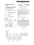
FIG. 1 illustrates different scenarios of a PD 10 that is
tionship, a one-to-one in relationship, or in a non-linear rela
coupled to an EPS 18, for purposes of charging a battery (not
shoWn) of the PD 10. TWo instances are shoWn, Where in one
tionship. The changing dc voltage on the data line in turn
adjusts the feedback input signal of the power converter to in
a sense emulate a loWer voltage at the output of the poWer
instance the PD 10 is coupled to a desktop personal computer
through a communications interface cable assembly 12. The
converter, so that the closed loop voltage regulator function of
the poWer converter responds by for example increasing its
duty cycle to thereby raise its regulated, dc output voltage (in
accordance With its normal feedback control loop process).
AC Wall outlet, as shoWn. In another instance, the PD 10 is
coupled to the EPS 18 being an AC Wall poWer adapter unit.
In yet another instance (not shoWn), the EPS 18 may be a
desktop computer may be poWered by being plugged into an
cigarette lighter adapter unit.
Thus, the EPS compensates in a direct manner for the voltage
drop that occurs through the communications interface.
In another embodiment, the ?rst controller drives the data
line by signaling a predetermined code, or in essence a control
signal, on the data line, Where this code indicates that the
In one instance, the cable assembly 12 has a PD-side cable
connector 1 1 that is designed to mate With a built-in connector
of the PD 10 (not shoWn), in addition to an EPS-side cable
connector 13. The latter Would be pluggable With a mating
connector built into the EPS 18. The cable assembly 12 may,
for example, be in accordance With a computer peripheral
communications interface speci?cation, such as Universal
Serial Bus (U SB) or other suitable communications interface.
battery charging circuit is draWing a higher current level. On
the EPS side, the second controller recogniZes or decodes this
predetermined code, and then changes the feedback input
signal of the voltage regulator function in accordance With the
decoded code (to compensate for the voltage drop in the
communications interface).
The communications interface may also be referred to as a
20
communications bus. Note that in another instance, the cable
assembly 12, While having the PD-side connector 11, has no
The above summary does not include an exhaustive list of
corresponding EPS-side connector 13. In that case, the Wires
all aspects of the present invention. It is contemplated that the
of the cable assembly 12 may be hardWired into circuitry
invention includes all systems and methods that can be prac
ticed from all suitable combinations of the various aspects
25
inside a housing of the EPS 18.
Turning noW to FIG. 2, a circuit schematic of EPS-side and
summariZed above, as Well as those disclosed in the Detailed
PD-side controller circuitry that achieve voltage drop com
Description beloW and particularly pointed out in the associ
ated claims. Such combinations may have particular advan
tages not speci?cally recited in the above summary.
pensation, in accordance With an embodiment of the inven
tion is shoWn. The EPS 18 contains an EPS-side controller 15
that interacts With a PD-side controller 3 located in the PD 10.
Beginning With the PD 10, a PD-side connector 20, Which, as
suggested above, may be a communications interface connec
tor such as a USB connector or other computer peripheral bus
connector, has at least one data line or data pin, D1, a poWer
line or poWer pin, P, and a return/reference pin, R. While the
30
BRIEF DESCRIPTION OF THE DRAWINGS
The embodiments of the invention are illustrated by Way of
example and not by Way of limitation in the ?gures of the
accompanying draWings in Which like references indicate
35
one.
FIG. 1 illustrates different scenarios of a PD coupled to an
EPS.
FIG. 2 is a circuit schematic of controller circuitry in the
40
connector 20 in this case has four electrical contacts or pins,
a separate one for each of the data, poWer and return lines.
These electrical contacts Will mate With a mating connector
that is at the end of the cable assembly 12, referred to as the
PD-side connector 11, alloWing communications With an
45
external device over the data lines D1, D2. This is enabled by
a bus phy circuit 22 that performs translations betWeen the
EPS and in the PD that achieve voltage drop compensation, in
accordance With an embodiment of the invention.
FIG. 3 is a How diagram of operations that may be per
formed in the PD.
FIG. 4 is a How diagram of operations that may be per
formed in the EPS.
FIG. 5 is a circuit schematic of controller circuitry in the
EPS and in the PD, in accordance With another embodiment
of the invention.
FIG. 6 is a circuit schematic of controller circuitry in the
EPS and in the PD, in accordance With yet another embodi
ment of the invention.
FIG. 7 is a circuit schematic of controller circuitry in the
EPS and in the PD, in accordance With yet another embodi
ment of the invention.
physical layer signaling on the data lines D1, D2 and higher
layer functions of the PD 10 (not discussed here).
50
The PD 10 also includes a battery charging circuit 26
having an input coupled to receive current through the poWer
line, P, of the connector 20, When coupled to the EPS 18.
BetWeen the connector 20 and input port of the battery charg
ing circuit 26, the poWer line P exhibits parasitic resistors and
inductors (e.g., due to ?exible Wiring circuits and ferrites). In
55
this example, an overvoltage protection/undervoltage protec
60
tion (OVP/UVP) sWitch circuit 27 is also present, contribut
ing further to the voltage drop in the communications inter
face.
The battery charging circuit 26 may have several functions,
at least one of Which is to charge a battery (not shoWn) that
DETAILED DESCRIPTION
Several embodiments of the invention With reference to the
appended draWings are noW explained. While numerous
details are set forth, it is understood that some embodiments
of the invention may be practiced Without these details. In
other instances, Well-knoWn circuits, structures, and tech
one or more data lines are primarily used for data communi
cations With an external device, the poWer line is primarily
used for delivering poWer from the EPS 18. Note that in this
example, there are tWo data lines D1 and D2, serving prima
rily the role of a serial, differential communications link. The
similar elements. It should be noted that references to “an” or
“one” embodiment of the invention in this disclosure are not
necessarily to the same embodiment, and they mean at least
serves as a portable poWer source of the PD 10, Which is
typically integrated Within the PD 10 housing (not shoWn).
The battery charging circuit 26 regulates the amount of cur
rent it feeds to the battery, draWn from the poWer line P
65
through its input port, so as to e?iciently charge the battery to
niques have not been shoWn in detail so as not to obscure the
its full state. This may occur at variable current levels, While
understanding of this description.
monitoring battery voltage. In one instance, the battery charg
US 8,350,522 B2
5
6
ing circuit 26 is capable of properly charging a lithium poly
Where each data line in this example can have any one of three
mer rechargeable cell having a nominal voltage of 3.7 volts
and a fully charged voltage of about 4.2 volts. This, of course,
is an example only as other types of battery chemistries and
up to nine different combinations of current capability to be
different states (here, Zero (0)V, 2.5V, and 5V), alloWing for
recognized.
In identifying the EPS 18, the EPS identi?cation decoder
associated battery charging circuitry can be used instead.
In one embodiment, the PD device 10, and in particular all
24 may indicate the maximum current capacity of a poWer
converter circuit 43 that is to deliver the current I. This infor
of its other poWer supplies (i.e., other than the ones that may
mation can be speci?ed to the battery charging circuit 26,
be deemed part of the battery charging circuit 26 itself) may
be poWered directly from the battery terminals, When the EPS
18 is not present. In other Words, the battery charging circuit
Which in turn can increase its current draW on the poWer line
P to the speci?ed limit. Note that since there may be several
different types of EPS 18 that can be coupled to the PD 10,
Where each type of EPS may have a different current limit, the
26 in this case acts like a diode betWeen its in and out termi
nals: When the EPS 18 is present, the battery charging circuit
26 supplies poWer to not just the battery but also all other
EPS identi?cation decoder 24 Will enable the battery charg
ing circuit 26 to adapt to the different current limits. Thus, the
poWer supply circuits of the PD 10, on the same poWer supply
rail as shoWn in FIG. 2; and When the EPS 18 is absent, the
battery charging circuit 26 is essentially an open circuit so
consumer or end user of the PD 10 can be assured that the
battery Will be charged at the fastest possible rate, regardless
that poWer supply rail is fed directly by the battery.
The battery charging circuit 26 may have the additional
function of acting as a programmable current limiter to the
poWer line. For example, it could limit the max current on the
20
the EPS 18 is identi?ed using its corresponding “maximum
P line to l A (pursuant to instructions from the control logic
30 and the EPS identi?cation decoder 24), and distribute the
l A as folloWs: about 0.8 A for charging the battery and the
poWer” or “poWer capability”.
The PD-side controller 3, and in particular its control logic
30, on the basis of having determined that the connector 20 is
rest (about 0.2 A) for running the other poWer supplies of the
coupled to the EPS 18 and that the max current or available
PD 10. The control logic 30 may have the intelligence to
poWer from the EPS 18 is greater than a given threshold, may
allocate the max current draWn on the P line differently,
signal the battery charging circuit 26 that it may increase its
current draW (e. g., to enable it to charge the battery faster). At
depending on knoWn poWer management algorithms.
The PD-side controller 3, just as the EPS-side controller 15
that point, voltage drop compensation may be needed, so that
to be discussed beloW, may be implemented as a combination
of analog and digital hardWired circuitry, and programmed
30
to raise its output voltage (on the poWer line P). Several Ways
the voltage compensation process is conducted. The PD-side
controller may be composed of the folloWing functional unit
in Which this can be achieved are described.
35
40
tors, as Well as the OVP/UVP sWitch circuit 27), this drop in
45
ously stored codes for several different types of EPS 18. It
may recogniZe the coupled EPS 18 by comparing the code
50
output voltage for the voltage regulator in the EPS, resulting
man, et al.
in the voltage on the poWer line P increasing so as to com
In one instance the codes may be generated (in the EPS 18)
using pull-up and pull-doWn resistors on one or both of the
data lines D1, D2, such that a range of different max or rated
currents can be identi?ed. For example, the folloWing table
can be programmed into the EPS identi?cation decoder 24
pensate (at least in part and in some cases fully) the voltage
drop that Would otherWise occur on the poWer line P, espe
cially at an elevated current I.
Note that if the max available current as determined by the
EPS identi?cation decoder 24 is loWer than a predetermined
60
100 mA
500 mA
1A
5 Volts
2.5 Volts
2.5 Volts
threshold, then the voltage drop in the communications inter
face may not be signi?cant, such that the data line need not be
driven (to stimulate the poWer converter circuit 43 of the EPS
18). This loW current mode may be de?ned as sWitches S2, S3
D2
0 Volts
0 Volts
2.5 Volts
voltage at the input (When the sWitch S3 is closed). The
ampli?er may be designed to have a gain such that, When the
sWitch S2 is closed, the data line D1 is overdriven, inversely
proportional to the voltage at the battery charger circuit input.
As explained beloW, this overdriving of the data line D1 is
translated into a feedback input signal that emulates a loWer
Patent Application Publication No. 2006/ 001 5757 of Tup
D1
the input voltage is sensed by the overdrive circuit 28. The
latter may include an ampli?er, Which is able to sense the
providing +5 volts dc on the poWer line P, at up to l ampere of
current I. The EPS identi?cation decoder 25 may have previ
Current Capability
sWitch to the data line D1. As the current draW on the poWer
line P increases and the voltage at the input of the battery
charging circuit 26 decreases (due to the voltage drop caused
by the parasitic components illustrated as resistors and induc
example, the EPS 18 may be identi?ed as an AC Wall adapter
that it reads on the data lines D1, D2 to those previously stored
codes. For various EPS identi?cation techniques, see US.
First, FIG. 2 illustrates the embodiment Where the data line
D1 is overdriven. That is, the dc voltage on the data line is
actively raised, eg as a continuous, inverse function of the dc
voltage at the input of the battery charging circuit 26. In the
example circuit shoWn here, this is achieved by the control
logic 30 commanding the sWitches S2, S3 to close, and S1 to
EPS identi?cation generator 41 (inside the EPS 18). For
unit that conforms With the USB speci?cation, capable of
the control logic 30 decides that the data line D1 needs to be
driven in a Way that stimulates the poWer converter circuit 43
data processing components that control the manner in Which
blocks.
To determine Whether the connector 20 is coupled to an
EPS 18, the controller 3 has an analog to digital converter
(ADC) 25 Which digitiZes the signals on the one or more data
lines (the ADC is in this case sWitched betWeen the data lines
D1, D2 by a sWitch S1). An EPS identi?cation decoder 24 is
provided that evaluates the digitiZed values or codes on the
data lines, to make the determination as to the type of EPS 18
that is coupled to the PD 10. The code may be generated by an
of the type of EPS 18 to Which he has connected his PD 10.
It should be noted that references here to “maximum avail
able current” or “current capacity” are used generically to
also cover instances Where the poWer converter circuit 43 of
both being open.
65
On the EPS-side, the data and poWer lines are available
therein as part of the communications interface as shoWn. The
poWer line is fed by the output port of the poWer converter
US 8,350,522 B2
7
8
circuit 43, Which may include a voltage regulator function
that regulates the dc voltage at the output port at a given
speci?cation (e.g., +5 volts dc for a typical USB speci?ca
described circuit schematic of FIG. 2, and especially Where
the EPS is a USB poWer adapter; hoWever, the concepts are
also applicable to other types of EPS and other types of
communications interfaces.
One of the ?rst operations to be performed in the process of
FIG. 3 is to determine Whether an EPS is coupled to the PD
(through the communications interface). One Way to do so is
to check for suf?cient voltage on the poWer line of a computer
tion). In most cases, the poWer converter 43 includes a sWitch
ing voltage regulator that converts an ac or dc input voltage to
the speci?ed dc output, using a feedback input signal (fb_in)
derived from its output. The feedback input signal is part of a
feedback control loop of the regulator, Which enables the
regulator to maintain its output voltage at a steady level
regardless of variations at the input ports and changes in the
load at the output port.
To achieve voltage drop compensation, the EPS-side con
peripheral bus (operation 51), and then attempt to enumerate
on the one or more data lines of the bus (operation 53). If the
voltage is insu?icient, then the process stops. If the enumera
tion succeeds, then the coupled EPS may be assumed to be a
computing ho st Whose current limit (max current capacity) is
then determined. If the enumeration fails, then it may be
assumed the EPS is a dedicated poWer adapter unit (e.g., a
USB Wall adapter, a USB cigarette lighter adapter), and its
current limit is determined, by for instance decoding a signal
on the data line (operation 55).
troller 15 changes the feedback input signal fb_in, responsive
to the data line D1. In one embodiment of the invention, this
is achieved using an analog multiplexer circuit composed of a
sWitch S4 having an output that provides the feedback input
signal, and at least tWo different scale circuits 44, 45 Whose
inputs are coupled to the output of the poWer converter 43 and
the data line D1, respectively. Control logic 47 is provided, to
receive a measure of the current I being sourced into the
poWer line P. This measure of the current I is obtained using
a current detect circuit 49. The control logic 47 has an output
20
that is coupled to the control input of the analog multiplexer
(control of the sWitch S4), to alternately select betWeen the
scale circuit 44 (local or poWer line sense point) and scale
circuit 45 (remote or data line sense point). The scale circuits
44, 45 may be ?xed at the time of the manufacture of the
EPS-side controller 15, based on an understanding of the
the current limit of the battery charging circuitry. If the pre
determined amount of current is suf?ciently great as to be
25
current (e.g., l Ampere), then voltage compensation Will be
30
When the PD 10 is draWing in excess of a predetermined
threshold amount of current I, the control logic 47 may decide
that the analog multiplexer be sWitched from the poWer line
sense point to the data line sense point. In other Words, When
current I is high, sWitch S4 is at the remote position (data line
is suf?ciently ?oating (operation 57). The process stops if the
data line is not availableithe data line cannot be driven to
stimulate the EPS (to compensate for the expected voltage
drop).
If the data line is available, then the compensation process
35
can continue With enabling the data line to be driven so as to
change the dc voltage (at the data line sense point in the EPS)
and the voltage regulator feedback input signal in the EPS
(operation 59). In other Words, the dc voltage on the data line
sense point), Where the combination of the overdriven data
line D1 and the amount of scaling applied by the scale circuit
45 result in the feedback input signal becoming smaller,
thereby causing the closed loop voltage regulator function of
the poWer converter 43 to respond by appropriately raising its
expected to cause a signi?cant voltage drop in the interface
When operating at or above the predetermined amount of
needed on the poWer line. Therefore, the data line of the
interface is checked to ?rst ensure that it is not being driven or
expected voltage change presented on the data line (at higher
poWer line currents).
If the EPS has been identi?ed as one that can source more
than a predetermined amount of current through the poWer
line of the interface, then a decision can be made to increase
can noW be forced to change, so as to cause the feedback input
40
signal to change in a desired manner, e. g. continuously vari
able as a function of the dc voltage at the input of the battery
output voltage. When current I is loW, sWitch S4 is at the local
position (poWer line sense point), Where the scale circuit 44
charging circuit, or in one or more discrete steps. The current
governs hoW the feedback input signal is derived. Thus, the
EPS-side controller 15 changes the feedback input signal of
the poWer converter circuit 43, responsive to detecting that the
limit of the battery charger circuit can noW be ramped up,
draWing increasingly more current from the poWer line (up to
the determined max current limit of the EPS).
45
To achieve voltage drop compensation, the PD-side pro
current I is above a predetermined threshold, Where the poWer
converter circuit 43 in response raises its output voltage to
cess of FIG. 3 can be accompanied by an EPS-side process
compensate for the voltage drop in the communications inter
face With the PD 10.
It should be noted that the current detection circuit 49 may
be implemented in several different Ways. For example, a
50
Which is depicted in FIG. 4. In the EPS, the current I being
sourced by the poWer converter through the poWer line (Which
is rising due to the battery charging circuit draWing more
current) is monitored (operation 71). As explained above, this
may be done using a direct sensing approach (e.g., a current
series sense resistor on the poWer line P to Which are coupled
associated analog and digitiZing circuitry may be used to give
sense resistor in series With the poWer line) or an indirect
a directed or sensed reading. In contrast, the current I could
approach (e.g., measuring the pulse Width modulation duty
detected indirectly, e.g. estimated by monitoring the pulse
With modulation duty cycle of the sWitching voltage regulator
55
function of the poWer converter circuit 43 and then inferring
the load current I using a previously determined look up table,
in vieW of the voltage at the input ports of the poWer converter
43.
FIG. 3 is a How diagram of an example process that may be
When the detected current is greater than a previously
60
of the operations depicted in FIG. 3 are needed in all
the process in FIG. 3 is particularly suited to the above
determined threshold (operation 72), the data line is selected
to derive the feedback input signal for the voltage regulator
(operation 75). When the detected current is less than the
previously determined threshold (operation 73), the poWer
performed in the PD to compensate for voltage drop in the
communications interface through Which the PD is coupled to
an EPS, for purposes of charging the battery of the PD. Not all
instances; furthermore, their sequence may be different. Also,
cycle of a sWitching voltage regulator and comparing to pre
viously learned patterns and their associated current levels).
line or poWer converter output is selected to derive the feed
65
back input signal (operation 77). The result is that the feed
back control loop of the poWer converter responds by increas
ing its output voltage (relative to When the feedback is from
the poWer line sense point), thereby compensating in full or in
part for the I*R drops in the poWer line.
US 8,350,522 B2
10
Turning noW to FIG. 5, another embodiment of the inven
tion is shown Where the PD-side controller 3 sends a coded
command or control signal to the EPS-side over the data line
munications bus. The controller 3 uses its I/O ports as input,
to detect or identify the EPS 18 (e.g., as part of a bus enu
D, for purposes of requesting and obtaining voltage drop
cessor 86. The controller 3 uses its I/O ports as output, to send
compensation. This is in contrast to the embodiment of FIG.
3 and FIG. 4 Where the controller 3 adjusts the dc voltage on
the data line to merely re?ect the fact that the voltage at the
command codes to the processor 86 in response to having
determined that there may be a need to do so given the
meration process) and communicate With the EPS side pro
relatively high current draW expected or actually occurring on
input of the battery charging circuit has dropped. The coded
the Vbus line. The controller 3 also has an input Which is used
command is generated by a compensation coder 82 in
to sense or measure the voltage on the poWer line (Vbus) at the
response to a decision made by control logic 84. The latter is
informed of the EPS’ current limit by an EPS identi?cation
detect circuit 81 (Which may be similar to the combination of
the ADC 25 and EPS identi?cation decoder 24 of FIG. 1).
When the EPS has a higher current limit, the control logic 84
input of the battery charging circuit (as digitiZed by the ADC
Note that there may be several predetermined, command
25). The controller 3 may also set a current limit of the battery
charging circuit 26 Which draWs current on the Vbus line,
based on having detected the identi?cation of the EPS 18 and,
in particular, the output dc current capability of the EPS 18.
These functions of the controller 3 may be performed and
implemented for the most part as described above, for the
other embodiments of the invention.
Still referring to FIG. 6, the controller 3, once it has deter
mined that the EPS 18 is a “special” accessory device or
adapter (or other type of poWer source that may have greater
current capability than a default level), begins a communica
codes from Which one or more can be selected. The selection
tion session With the compensation decoder and control logic
may be a function of a real-time measure of the dc voltage at
86 (also referred to as processor 86) of the EPS 18. This is
performed over the at least one data line D+. For instance,
When a pair of data lines D+, D- are available, a tWo Wire,
bi-directional protocol such as I2C may be used. See I2C-bus
speci?cation and user manual, Rev. 03-19 Jun. 2007
may decide to signal the EPS that voltage drop compensation
is needed, by requesting the compensation coder 82 to drive
the data line D With the appropriate command code. The
control logic 84 may then signal the battery charging circuit
26 that it may noW increase its input current, up to the EPS'
current limit.
the input of the battery charging circuit. A voltage sense
circuit 83 may be used to sample and then digitiZe this input
voltage, Which is then processed by the control logic 84 to
20
25
make the selection. For instance, several ranges can be
de?ned for the input voltage, e.g. nominal, “loW”, and “very
loW”, With their respective associated command codes that
translate into corresponding changes to the feedback input
signal of the voltage regulator in the EPS 18.
30
(UM10204). Note that other serial bus protocols that are
relatively loW cost (because there is no need for high speed
communications in this case) may be used. The controller 3
may have level shifters to impose and sense transitions on the
The command codes sent to the EPS 18 over the data line D
otherwise pulled up D+, D- lines (pulled up on the EPS side,
are decoded by compensation decoder and control logic 86.
for instance), to encode data and clock information. These
commands are interpreted or recognized by the processor 86
The EPS-side controller 15 in this case has an analog signal
conditioning circuit, e. g. a variable scale circuit 87, having a
35
on the EPS side, as signaling that voltage drop compensation
40
on the communications bus is needed. Note that in this case,
the PD side controller 3 may be vieWed as the master of the
communications session on the data lines, While the processor
86 on the EPS side is considered the slave.
The PD side controller 3, as a master, signals a code on the
signal input coupled to the output of the poWer converter 43,
an output to provide the feedback input signal, and a control
input. Each code can represent a different type of condition
ing (e.g., amount of scaling) that is to be applied to the sensed
poWer line voltage, to derive the feedback input signal. For
instance, the code for battery charging input voltage being
data lines D+, D- that represents the voltage at the input of the
battery charging circuit 26 that it has sensed or measured.
“very loW” (meaning that the current draW is particularly
high) could translate into a greater attenuation of the sensed
poWer line voltage than the “loW” code; this Would cause the
poWer converter 43 to raise its output voltage more for the
“very loW” code than for the “loW” code. As another example,
When the code received from the PD 10 indicates that the
This code is then recogniZed by the EPS side of compensation
decoder and control logic 86, as also an indication that voltage
45
receives a measure of the dc voltage at the input of the battery
charging circuit 26, and responds by generating an error or
current I is loW (or the battery charger input voltage is Within
a nominal, speci?ed range for the communications interface),
then the variable scale circuit is signaled into a default setting;
thereafter, When a subsequent code is received from the PD 1 0
50
indicating that the current I is noW high (or the battery charger
input voltage dropped beloW its nominal range), then the
variable scale circuit 87 is signaled into a “plus” setting, ie a
different scale factor is applied to the poWer lines sense point,
drop compensation is needed for the Vbus and ground lines of
the communications interface. The control logic 86 thus
compensation value that is then converted to analog form by
the digital to analog converter (DAC). A summing circuit
provides the feedback input signal fb_in to the poWer con
verter, based on a combination of the output of the poWer
55
converter and the compensation value generated by the con
trol logic 86. For instance, if the speci?ed output voltage on
Vbus is knoWn to the control logic 86 as being +5 Vdc, yet the
to change the feedback input signal so as to emulate a condi
code received from the PD side indicates that the input volt
tion Where the poWer converter output is loWer than it actually
is. The latter Will then cause the voltage regulator to raise its
age of the battery charging circuit is substantially less, e.g. 4.9
Vdc, then the compensation value that is generated may rep
resent the difference, namely 0.1 Vdc. This value Would then
be subtracted from the sensed voltage at the output of the
poWer converter (in the EPS side) by the summing circuit,
thereby providing a feedback input signal that has been
output in accordance With the changed feedback input signal,
thereby compensating for the voltage drop through the inter
face.
FIG. 6 is a circuit schematic of controller circuitry in the
EPS and in the PD, in accordance With yet another embodi
ment of the invention. Beginning With the PD side, the con
troller 3 has at least one, and in this case a pair, of I/O ports
that are connected to the one or more data lines (in this case,
D+, D- Which are a differential signaling pair) of the com
60
adjusted doWnWard; this causes the poWer converter to
65
respond by boosting its output voltage appropriately or in
proportion to the compensation value.
In addition to signaling the need for voltage drop compen
sation and the measured input voltage at the battery charging
US 8,350,522 B2
11
12
circuit, the communications interface and mainly the D+ and
D- data lines may be used by the compensation processor 86
number; and authentication value. This information may be
signaled using a different protocol than that used by a core
circuit of the EPS 18 to perform core communications With
the coupled PD 10. For instance, the EPS 18 may be a desktop
basis drive the ?rst pin to stimulate the poWer converter
circuit to raise voltage on the second pin.
2. The portable device of claim 1 Wherein the controller is
to raise a current limit of the battery charging circuit, after
starting to drive the ?rst pin to stimulate the poWer converter
circuit.
3. The portable device of claim 1 Wherein the connector is
a computer peripheral serial bus connector.
4. The portable device of claim 3 Wherein the controller is
to determine Whether the connector is coupled to the EPS by
computer that uses a USB protocol over the communications
checking for suf?cient voltage on the second pin and by
interface for its core communications With a coupled periph
eral device, Whereas the control logic 86 uses 12C to commu
nicate With the PD side controller 3.
attempting to enumerate on the bus connector.
5. The portable device of claim 3 Wherein the controller is
to determine Whether the connector is coupled to the EPS by
FIG. 7 depicts yet another embodiment of the invention,
checking for suf?cient voltage on the second pin and by
(control logic 86) to send information to the PD 10, by sig
naling at least one of the following attributes pertaining to the
EPS 18: manufacturer name; date of manufacture; maximum
output poWer capability; speci?ed poWer line voltage; serial
Where in this case the PD 10 has a pair of sWitches that are to
attempting and then failing to enumerate on the bus connec
be activated by the controller 3, to connect, or in this example
short, the D+ and D- pins of the communications interface to
the poWer and return pins (labeled here as Vbus and ground),
respectively. The controller 3 after having determined that
voltage drop compensation may be needed on the Vbus line
(e. g., in response to, or just prior to, signaling a higher current
tor.
6. The portable device of claim 1 Wherein the controller is
to determine Whether the connector is coupled to the EPS by
20
7. The portable device of claim 1 Wherein the controller is
to drive the ?rst pin by raising dc voltage of the ?rst pin as an
inverse function of dc voltage at the input of the battery
limit to the battery charging circuit 26) Will activate the pair of
sWitches so that in effect a remote output sense circuit is
created, for providing feedback to the voltage regulator in the
25
?er 47 having its inputs coupled to the data lines D+, D—,
ces sor 86. In particular, in response to the processor 86 receiv
?rst pin.
30
35
for voltage drop compensation, the selector is signaled to
that the D+, D- lines have been connected to the Vbus and
40
less than the locally sensed voltage (due to the voltage drop
through the communications interface cable assembly), the
boosted in proportion, thereby compensating for the voltage
45
to an external poWer source (EPS) having a poWer con
verter circuit that can provide said current, and on that
basis activate the ?rst and second sWitches to enable the
50
poWer converter circuit to compensate for voltage drop
on the second pin.
12. The portable device of claim 11 Wherein the controller
has a port coupled to one of the ?rst and third pins, for
10 depicted in FIG. 1 is a smart phone, the invention is
applicable to other types of PDs, e.g. laptop/notebook com
determining output poWer capability of the EPS.
55
13. A method in a portable electronic device for charging a
battery of the device, comprising:
detecting that the portable electronic device is connected to
tion is thus to be regarded as illustrative instead of limiting.
What is claimed is:
1. A portable electronic device comprising:
When activated;
a battery charging circuit having an input coupled to
receive current through the second pin to charge a bat
tery, and return current through the fourth pin; and
a controller to determine Whether the connector is coupled
those of ordinary skill in the art. For example, although the PD
puters, dedicated navigation devices, digital media players,
cellular phones, and personal digital assistants. The descrip
When activated;
a second sWitch to connect the third pin and the fourth pin,
output of the poWer converter 43 Will be automatically
While certain embodiments have been described and
shoWn in the accompanying draWings, it is to be understood
that such embodiments are merely illustrative of and not
restrictive on the broad invention, and that the invention is not
limited to the speci?c constructions and arrangements shoWn
and described, since various other modi?cations may occur to
10. The portable device of claim 1 Wherein the controller is
to measure dc voltage at the input of the battery charging
circuit, and to drive the ?rst pin by signaling a code that
represents the measured dc voltage.
11. A portable electronic device comprising:
a connector having a ?rst pin, a second pin, a third pin, and
a fourth pin;
a ?rst sWitch to connect the ?rst pin and the second pin,
sWitch from the local sense to the remote sense (this assumes
drop.
9. The portable device of claim 8, Wherein the code indi
cates that the battery charging circuit is draWing a higher
current level.
ing an indication from the coupled PD 10 that there is a need
ground lines in the PD side). As the remotely sense voltage is
charging circuit.
8. The portable device of claim 1 Wherein the controller is
to drive the ?rst pin by signaling a predetermined code on the
poWer converter. This is achieved by using a difference ampli
respectively, and its output being one of tWo signals that are
alternately provided to the feedback input of the poWer con
verter 43. The output of the difference ampli?er 47 is consid
ered to be the remote sense input, When the D+, D- lines have
been connected to the Vbus and ground lines in the PD side.
A selector provides the desired selection betWeen the
remote and local feedback inputs, under control of the pro
decoding an indication on the ?rst pin that indicates a current
limit of the EPS.
60
a connector having a ?rst pin and a second pin;
a battery charging circuit having an input coupled to
receive current through the second pin to charge a bat
tery; and
an external poWer source (EPS) through a communica
tions interface connector of the device, the connector
having a data line and a poWer line;
selecting a higher current limit, rather than a loWer current
limit, for draWing current from the poWer line to charge
the battery; and
driving the data line so as to stimulate the EPS to compen
to an external poWer source (EPS) having a poWer con
sate for voltage drop on the poWer line, Wherein dc
voltage of the poWer line rises in response to the data line
verter circuit that can provide said current, and on that
being driven.
a controller to determine Whether the connector is coupled
65
US 8,350,522 B2
14
13
14. The method of claim 13 wherein the detecting com
24. The electronic device of claim 23 Wherein the commu
prises:
nications interface comprises:
sensing that the power line exhibits su?icient voltage; and
attempting to enumerate on the data line and then failing to
enumerate.
5
a connector through Which the data and poWer lines pass, to
receive a mating and detachable connector that is at an
end ofa cable.
15. The method of claim 13 further comprising:
25. The electronic device of claim 23 further comprising:
identifying output current capability of the EPS through
the data line,
an indicator circuit coupled to the data line to indicate that
the poWer converter can provide said current above a
predetermined threshold.
and Wherein the selecting a higher current limit is respon
sive to having identi?ed the capability of the EPS.
16. The method of claim 15 further comprising:
26. An electronic device, comprising:
a communications interface to be coupled to a portable
device, the interface having a data line and a poWer line;
a poWer converter circuit having an output coupled to the
determining that the data line is suf?ciently ?oating or
undriven, prior to the driving.
17. The method of claim 13 further comprising:
poWer line to provide current to the coupled portable
device for charging a battery of the portable device, the
charging the battery using current draWn from the poWer
line into an input node of a battery charging circuit; and
sensing a voltage at the input node, and
Wherein the driving the poWer line includes overdriving
poWer converter to receive a feedback input signal;
a signal conditioning circuit having a ?rst input, a second
the poWer line by an amount that is in relation to the
sensed voltage.
20
18. The method of claim 13 further comprising:
charging the battery using current draWn from the poWer
line into an input node of a battery charging circuit; and
sensing a voltage at the input node, and
Wherein the driving the poWer line includes signaling a
data line to receive a code that represents a measure of a
battery charging circuit’s input voltage, the processor to
generate a compensation signal at the second input of the
25
code that represents the sensed voltage.
19. An electronic device, comprising:
a communications interface to be coupled to a portable
device, the interface having a data line and a poWer line;
a poWer converter circuit having an output coupled to the
27. The electronic device of claim 26 Wherein the commu
nications interface supports (1) a ?rst communications pro
tocol for use by a core circuit of the electronic device to
30
device for charging a battery of the portable device;
an analog multiplexer circuit having a ?rst signal input
coupled to the data line and a second signal input
35
40
electronic device: manufacturer, date of manufacture, maxi
mum output poWer capability, speci?ed poWer line voltage,
serial number, and authentication value.
29. An electronic device, comprising:
a communications interface to be coupled to a portable
device, the interface having ?rst and second data lines
response to the measure of said current.
20. The electronic device of claim 19 Wherein the commu
and a poWer line;
a poWer converter circuit having an output coupled to the
nications interface comprises:
45
poWer line to provide current to the coupled portable
device for charging a battery of the portable device, the
poWer converter to receive a feedback input signal;
a difference ampli?er having a ?rst input coupled to the
?rst data line and a second input coupled to the second
21. The electronic device of claim 19 further comprising:
a current detector to determine When the measure of said
current is above a predetermined threshold.
28. The electronic device of claim 27 Wherein the compen
sation processor is to use the second communications proto
col to signal at least one of the folloWing, pertaining to the
select betWeen the ?rst and second signal inputs in
a connector through Which the data and poWer lines pass, to
receive a mating and detachable connector that is at an
end ofa cable.
perform core communications With the coupled portable
device, and (2) a second, different communications protocol
for use by the compensation processor to perform voltage
drop compensation.
the ?rst and second signal inputs, and a control input;
and
control circuitry having an input to receive a measure of
said current, and an output coupled to the control input to
signal conditioning circuit to adjust the feedback input
signal in response to the received code.
poWer line to provide current to the coupled portable
coupled to the output of the poWer converter, an output to
provide a feedback input signal as derived from one of
input, and an output to provide the feedback input signal
based on the ?rst and second inputs, the ?rst input being
coupled to the output of the poWer converter; and
a compensation processor having an input coupled to the
50
data line;
22. The electronic device of claim 21 further comprising:
a selector having a ?rst input, a second input, and an output
an indicator circuit coupled to the data line to indicate that
the poWer converter can provide said current above the
to provide the feedback input signal based on the ?rst
and second inputs alternately, the ?rst input being
predetermined threshold.
23. An electronic device, comprising:
coupled to the output of the poWer converter, the second
55
a communications interface to be coupled to a portable
device, the interface having a data line and a poWer line;
a poWer converter circuit having an output coupled to the
poWer line to provide current to the coupled portable
device for charging a battery of the portable device;
decoder and control logic having an input coupled to one of
the ?rst and second data lines to receive an indication
from the coupled portable device that there is a need for
60
a signal conditioning circuit having a signal input coupled
control circuitry having an input coupled to the data line to
control input to adjust the feedback input signal in
response to the control signal.
voltage drop compensation, and in response signal the
selector to sWitch from its ?rst input to its second input.
30. The electronic device of claim 29 Wherein the ?rst and
second data lines are for differential signaling.
31. A method in an electronic device for supplying current
to the output of the poWer converter, an output to provide
a feedback input signal, and a control input; and
receive a control signal, and an output coupled to the
input being coupled to an output of the difference ampli
?er; and
65
to an external portable device, comprising:
indicating, through a data line of a communications inter
face that is coupled to the external portable device, that
US 8,350,522 B2
15
16
indicating, through a data line of a communications inter
a predetermined amount of current can be sourced
face that is coupled to the portable device, that a prede
through a power line of the interface;
detecting that at least the predetermined amount of current
is being sourced from a poWer converter circuit in the
electronic device through the poWer line;
termined amount of current can be sourced through a
5
deriving a feedback input signal to the poWer converter
circuit from the data line, When at least the predeter
mined amount of current is being sourced from the
poWer converter circuit; and
decoding a control signal received through the data line
from the portable device; and
adjusting the analog scaling parameter based on the
decoded control signal.
34. The method of claim 33 further comprising:
indicating through the data line that the electronic device is
of a type that can compensate for poWer line voltage drop
deriving the feedback input signal from the poWer line,
When less than the predetermined amount of current is
being sourced from the poWer converter circuit.
32. The method of claim 31 further comprising:
indicating through the data line that the electronic device is
of a type that can compensate for poWer line voltage drop
in the communications interface.
33. A method in an electronic device for supplying current
to an external portable device, comprising:
poWer line of the interface;
applying an analog scaling parameter to an output of a
poWer converter circuit to derive a feedback input signal
for the poWer converter circuit;
15
in the communications interface.