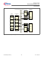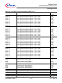
1
TriCore™
32-bit
TriCore™ V1.6
Core Architecture
32-bit Unified Processor Core
User Manual (Volume 1)
V1.0, 2012-05
Microcontrollers
Edition 2012-05
Published by
Infineon Technologies AG
81726 Munich, Germany
© 2012 Infineon Technologies AG
All Rights Reserved.
Legal Disclaimer
The information given in this document shall in no event be regarded as a guarantee of conditions or
characteristics. With respect to any examples or hints given herein, any typical values stated herein and/or any
information regarding the application of the device, Infineon Technologies hereby disclaims any and all warranties
and liabilities of any kind, including without limitation, warranties of non-infringement of intellectual property rights
of any third party.
Information
For further information on technology, delivery terms and conditions and prices, please contact the nearest
Infineon Technologies Office (www.infineon.com).
Warnings
Due to technical requirements, components may contain dangerous substances. For information on the types in
question, please contact the nearest Infineon Technologies Office.
Infineon Technologies components may be used in life-support devices or systems only with the express written
approval of Infineon Technologies, if a failure of such components can reasonably be expected to cause the failure
of that life-support device or system or to affect the safety or effectiveness of that device or system. Life support
devices or systems are intended to be implanted in the human body or to support and/or maintain and sustain
and/or protect human life. If they fail, it is reasonable to assume that the health of the user or other persons may
be endangered.
TriCore™
32-bit
TriCore™ V1.6
Core Architecture
32-bit Unified Processor Core
User Manual (Volume 1)
V1.0, 2012-05
Microcontrollers
TriCore™ V1.6
32-bit Unified Processor Core
TriCore™ V1.6 User Manual (Volume 1)
Revision History: V1.0 2012-05
Page
Subjects (major changes since last revision)
v1.0
TC1.6 First release
Trademarks
TriCore™ is a trademark of Infineon Technologies AG.
We Listen to Your Comments
Is there any information in this document that you feel is wrong, unclear or missing? Your feedback will help us to continuously
improve the quality of our documentation. Please send your proposal (including a reference to this document) to:
[email protected]
User Manual (Volume 1)
R-1
V1.0, 2012-05
TriCore™ V1.6
32-bit Unified Processor Core
Table of Contents
Table of Contents
1
1.1
1.1.1
1.2
1.2.1
1.2.2
1.2.3
1.2.4
1.3
1.4
1.4.1
1.5
1.6
1.7
1.8
Architecture Overview . . . . . . . . . . . . . . . . . . . . . . . . . . . . . . . . . . . . . . . . . . . . . . . . . . . . . . . . . .
Introduction . . . . . . . . . . . . . . . . . . . . . . . . . . . . . . . . . . . . . . . . . . . . . . . . . . . . . . . . . . . . . . . . . . . .
Feature Summary . . . . . . . . . . . . . . . . . . . . . . . . . . . . . . . . . . . . . . . . . . . . . . . . . . . . . . . . . . . . .
Programming Model . . . . . . . . . . . . . . . . . . . . . . . . . . . . . . . . . . . . . . . . . . . . . . . . . . . . . . . . . . . . .
Architectural Registers . . . . . . . . . . . . . . . . . . . . . . . . . . . . . . . . . . . . . . . . . . . . . . . . . . . . . . . . . .
Data Types . . . . . . . . . . . . . . . . . . . . . . . . . . . . . . . . . . . . . . . . . . . . . . . . . . . . . . . . . . . . . . . . . .
Memory Model . . . . . . . . . . . . . . . . . . . . . . . . . . . . . . . . . . . . . . . . . . . . . . . . . . . . . . . . . . . . . . . .
Addressing Modes . . . . . . . . . . . . . . . . . . . . . . . . . . . . . . . . . . . . . . . . . . . . . . . . . . . . . . . . . . . . .
Tasks and Contexts . . . . . . . . . . . . . . . . . . . . . . . . . . . . . . . . . . . . . . . . . . . . . . . . . . . . . . . . . . . . .
Interrupt System . . . . . . . . . . . . . . . . . . . . . . . . . . . . . . . . . . . . . . . . . . . . . . . . . . . . . . . . . . . . . . . .
Interrupt Priority . . . . . . . . . . . . . . . . . . . . . . . . . . . . . . . . . . . . . . . . . . . . . . . . . . . . . . . . . . . . . . .
Trap System . . . . . . . . . . . . . . . . . . . . . . . . . . . . . . . . . . . . . . . . . . . . . . . . . . . . . . . . . . . . . . . . . . .
Protection System . . . . . . . . . . . . . . . . . . . . . . . . . . . . . . . . . . . . . . . . . . . . . . . . . . . . . . . . . . . . . . .
Core Debug Controller . . . . . . . . . . . . . . . . . . . . . . . . . . . . . . . . . . . . . . . . . . . . . . . . . . . . . . . . . . .
TriCore Coprocessor Interface . . . . . . . . . . . . . . . . . . . . . . . . . . . . . . . . . . . . . . . . . . . . . . . . . . . . .
2
2.1
2.1.1
2.1.2
2.1.3
2.1.4
2.1.5
2.1.6
2.1.7
2.2
2.2.1
2.2.2
2.3
2.4
2.5
2.5.1
2.5.2
2.5.3
2.5.4
2.5.5
2.5.6
2.5.7
Programming Model . . . . . . . . . . . . . . . . . . . . . . . . . . . . . . . . . . . . . . . . . . . . . . . . . . . . . . . . . . . . 2-1
Data Types . . . . . . . . . . . . . . . . . . . . . . . . . . . . . . . . . . . . . . . . . . . . . . . . . . . . . . . . . . . . . . . . . . . . 2-1
Boolean . . . . . . . . . . . . . . . . . . . . . . . . . . . . . . . . . . . . . . . . . . . . . . . . . . . . . . . . . . . . . . . . . . . . . 2-1
Bit String . . . . . . . . . . . . . . . . . . . . . . . . . . . . . . . . . . . . . . . . . . . . . . . . . . . . . . . . . . . . . . . . . . . . 2-1
Byte . . . . . . . . . . . . . . . . . . . . . . . . . . . . . . . . . . . . . . . . . . . . . . . . . . . . . . . . . . . . . . . . . . . . . . . . 2-1
Signed Fraction . . . . . . . . . . . . . . . . . . . . . . . . . . . . . . . . . . . . . . . . . . . . . . . . . . . . . . . . . . . . . . . 2-1
Address . . . . . . . . . . . . . . . . . . . . . . . . . . . . . . . . . . . . . . . . . . . . . . . . . . . . . . . . . . . . . . . . . . . . . 2-1
Signed and Unsigned Integers . . . . . . . . . . . . . . . . . . . . . . . . . . . . . . . . . . . . . . . . . . . . . . . . . . . 2-1
IEEE-754 Single-Precision Floating-Point Number . . . . . . . . . . . . . . . . . . . . . . . . . . . . . . . . . . . . 2-2
Data Formats . . . . . . . . . . . . . . . . . . . . . . . . . . . . . . . . . . . . . . . . . . . . . . . . . . . . . . . . . . . . . . . . . . 2-2
Alignment Requirements . . . . . . . . . . . . . . . . . . . . . . . . . . . . . . . . . . . . . . . . . . . . . . . . . . . . . . . . 2-4
Byte Ordering . . . . . . . . . . . . . . . . . . . . . . . . . . . . . . . . . . . . . . . . . . . . . . . . . . . . . . . . . . . . . . . . . 2-5
Memory Model . . . . . . . . . . . . . . . . . . . . . . . . . . . . . . . . . . . . . . . . . . . . . . . . . . . . . . . . . . . . . . . . . 2-6
Semaphores and Atomic Operations . . . . . . . . . . . . . . . . . . . . . . . . . . . . . . . . . . . . . . . . . . . . . . . . 2-7
Addressing Modes . . . . . . . . . . . . . . . . . . . . . . . . . . . . . . . . . . . . . . . . . . . . . . . . . . . . . . . . . . . . . . 2-7
Absolute Addressing . . . . . . . . . . . . . . . . . . . . . . . . . . . . . . . . . . . . . . . . . . . . . . . . . . . . . . . . . . . 2-8
Base + Offset Addressing . . . . . . . . . . . . . . . . . . . . . . . . . . . . . . . . . . . . . . . . . . . . . . . . . . . . . . . 2-8
Pre-Increment and Pre-Decrement Addressing . . . . . . . . . . . . . . . . . . . . . . . . . . . . . . . . . . . . . . . 2-8
Post-Increment and Post-Decrement Addressing . . . . . . . . . . . . . . . . . . . . . . . . . . . . . . . . . . . . . 2-8
Circular Addressing . . . . . . . . . . . . . . . . . . . . . . . . . . . . . . . . . . . . . . . . . . . . . . . . . . . . . . . . . . . . 2-9
Bit-Reverse Addressing . . . . . . . . . . . . . . . . . . . . . . . . . . . . . . . . . . . . . . . . . . . . . . . . . . . . . . . . 2-11
Synthesized Addressing Modes . . . . . . . . . . . . . . . . . . . . . . . . . . . . . . . . . . . . . . . . . . . . . . . . . 2-12
3
3.1
3.2
3.3
3.4
3.5
3.5.1
3.6
3.7
3.8
3.9
General Purpose and System Registers . . . . . . . . . . . . . . . . . . . . . . . . . . . . . . . . . . . . . . . . . . . 3-1
General Purpose Registers (GPRs) . . . . . . . . . . . . . . . . . . . . . . . . . . . . . . . . . . . . . . . . . . . . . . . . . 3-2
Program State Information Registers . . . . . . . . . . . . . . . . . . . . . . . . . . . . . . . . . . . . . . . . . . . . . . . . 3-4
Stack Management Registers . . . . . . . . . . . . . . . . . . . . . . . . . . . . . . . . . . . . . . . . . . . . . . . . . . . . . 3-10
Compatibility Mode Register (COMPAT) . . . . . . . . . . . . . . . . . . . . . . . . . . . . . . . . . . . . . . . . . . . . 3-15
Access Control Registers . . . . . . . . . . . . . . . . . . . . . . . . . . . . . . . . . . . . . . . . . . . . . . . . . . . . . . . . 3-16
BIST Mode Access Control Register (BMACON) . . . . . . . . . . . . . . . . . . . . . . . . . . . . . . . . . . . . 3-16
Interrupt Registers . . . . . . . . . . . . . . . . . . . . . . . . . . . . . . . . . . . . . . . . . . . . . . . . . . . . . . . . . . . . . 3-18
Memory Protection Registers . . . . . . . . . . . . . . . . . . . . . . . . . . . . . . . . . . . . . . . . . . . . . . . . . . . . . 3-18
Trap Registers . . . . . . . . . . . . . . . . . . . . . . . . . . . . . . . . . . . . . . . . . . . . . . . . . . . . . . . . . . . . . . . . 3-18
Memory Configuration Registers . . . . . . . . . . . . . . . . . . . . . . . . . . . . . . . . . . . . . . . . . . . . . . . . . . 3-18
User Manual (Volume 1)
L-1
1-1
1-1
1-1
1-2
1-2
1-3
1-3
1-3
1-3
1-4
1-4
1-5
1-5
1-6
1-6
V1.0, 2012-05
TriCore™ V1.6
32-bit Unified Processor Core
Table of Contents
3.10
3.11
3.12
Core Debug Controller Registers . . . . . . . . . . . . . . . . . . . . . . . . . . . . . . . . . . . . . . . . . . . . . . . . . . 3-18
Floating Point Registers . . . . . . . . . . . . . . . . . . . . . . . . . . . . . . . . . . . . . . . . . . . . . . . . . . . . . . . . . 3-18
Accessing Core Special Function Registers (CSFRs) . . . . . . . . . . . . . . . . . . . . . . . . . . . . . . . . . . 3-18
4
4.1
4.1.1
4.2
4.3
4.4
4.5
4.6
4.7
4.7.1
4.7.2
4.8
4.8.1
4.8.2
4.9
4.10
Tasks and Functions . . . . . . . . . . . . . . . . . . . . . . . . . . . . . . . . . . . . . . . . . . . . . . . . . . . . . . . . . . . 4-1
Context Types . . . . . . . . . . . . . . . . . . . . . . . . . . . . . . . . . . . . . . . . . . . . . . . . . . . . . . . . . . . . . . . . . . 4-1
Context Save Area . . . . . . . . . . . . . . . . . . . . . . . . . . . . . . . . . . . . . . . . . . . . . . . . . . . . . . . . . . . . . 4-2
Task Switching Operation . . . . . . . . . . . . . . . . . . . . . . . . . . . . . . . . . . . . . . . . . . . . . . . . . . . . . . . . . 4-3
Context Save Areas (CSAs) and Context Lists . . . . . . . . . . . . . . . . . . . . . . . . . . . . . . . . . . . . . . . . 4-4
Context Switching with Interrupts and Traps . . . . . . . . . . . . . . . . . . . . . . . . . . . . . . . . . . . . . . . . . . 4-5
Context Switching for Function Calls . . . . . . . . . . . . . . . . . . . . . . . . . . . . . . . . . . . . . . . . . . . . . . . . 4-6
Fast Function Calls with FCALL/FRET . . . . . . . . . . . . . . . . . . . . . . . . . . . . . . . . . . . . . . . . . . . . . . . 4-6
Context Save and Restore Examples . . . . . . . . . . . . . . . . . . . . . . . . . . . . . . . . . . . . . . . . . . . . . . . . 4-7
Context Save . . . . . . . . . . . . . . . . . . . . . . . . . . . . . . . . . . . . . . . . . . . . . . . . . . . . . . . . . . . . . . . . . 4-7
Context Restore . . . . . . . . . . . . . . . . . . . . . . . . . . . . . . . . . . . . . . . . . . . . . . . . . . . . . . . . . . . . . . . 4-8
Context Management Registers . . . . . . . . . . . . . . . . . . . . . . . . . . . . . . . . . . . . . . . . . . . . . . . . . . . 4-10
Registers . . . . . . . . . . . . . . . . . . . . . . . . . . . . . . . . . . . . . . . . . . . . . . . . . . . . . . . . . . . . . . . . . . . 4-11
Free CSA List Limit Pointer Register (LCX) . . . . . . . . . . . . . . . . . . . . . . . . . . . . . . . . . . . . . . . . . 4-13
Accessing CSA Memory Locations . . . . . . . . . . . . . . . . . . . . . . . . . . . . . . . . . . . . . . . . . . . . . . . . . 4-13
Context Save Area Placement . . . . . . . . . . . . . . . . . . . . . . . . . . . . . . . . . . . . . . . . . . . . . . . . . . . . 4-13
5
5.1
5.1.1
5.2
5.2.1
5.2.2
5.2.3
5.3
5.4
5.5
5.6
5.6.1
5.6.2
5.6.3
5.6.4
5.6.5
5.6.6
5.6.7
Interrupt System . . . . . . . . . . . . . . . . . . . . . . . . . . . . . . . . . . . . . . . . . . . . . . . . . . . . . . . . . . . . . . . 5-1
Service Request Node (SRN) . . . . . . . . . . . . . . . . . . . . . . . . . . . . . . . . . . . . . . . . . . . . . . . . . . . . . . 5-1
Registers . . . . . . . . . . . . . . . . . . . . . . . . . . . . . . . . . . . . . . . . . . . . . . . . . . . . . . . . . . . . . . . . . . . . 5-3
Interrupt Control Unit (ICU) . . . . . . . . . . . . . . . . . . . . . . . . . . . . . . . . . . . . . . . . . . . . . . . . . . . . . . . . 5-6
ICU Interrupt Control Register (ICR) . . . . . . . . . . . . . . . . . . . . . . . . . . . . . . . . . . . . . . . . . . . . . . . 5-6
Interrupt Control Unit Operation . . . . . . . . . . . . . . . . . . . . . . . . . . . . . . . . . . . . . . . . . . . . . . . . . . . 5-6
Arbitration Scheme . . . . . . . . . . . . . . . . . . . . . . . . . . . . . . . . . . . . . . . . . . . . . . . . . . . . . . . . . . . . 5-7
Entering an Interrupt Service Routine (ISR) . . . . . . . . . . . . . . . . . . . . . . . . . . . . . . . . . . . . . . . . . . . 5-7
Exiting an Interrupt Service Routine (ISR) . . . . . . . . . . . . . . . . . . . . . . . . . . . . . . . . . . . . . . . . . . . . 5-8
Interrupt Vector Table . . . . . . . . . . . . . . . . . . . . . . . . . . . . . . . . . . . . . . . . . . . . . . . . . . . . . . . . . . . . 5-8
Using the TriCore Interrupt System . . . . . . . . . . . . . . . . . . . . . . . . . . . . . . . . . . . . . . . . . . . . . . . . 5-10
Spanning Interrupt Service Routines across Vector Entries . . . . . . . . . . . . . . . . . . . . . . . . . . . . 5-10
Interrupt Priority Groups . . . . . . . . . . . . . . . . . . . . . . . . . . . . . . . . . . . . . . . . . . . . . . . . . . . . . . . 5-10
Dividing ISRs into Different Priorities . . . . . . . . . . . . . . . . . . . . . . . . . . . . . . . . . . . . . . . . . . . . . . 5-11
Using Different Priorities for the Same Interrupt Source . . . . . . . . . . . . . . . . . . . . . . . . . . . . . . . 5-12
Software-Posted Interrupts . . . . . . . . . . . . . . . . . . . . . . . . . . . . . . . . . . . . . . . . . . . . . . . . . . . . . 5-13
Interrupt Priority Level One . . . . . . . . . . . . . . . . . . . . . . . . . . . . . . . . . . . . . . . . . . . . . . . . . . . . . 5-13
Interrupt Control Registers . . . . . . . . . . . . . . . . . . . . . . . . . . . . . . . . . . . . . . . . . . . . . . . . . . . . . . 5-14
6
6.1
6.1.1
6.1.2
6.1.3
6.1.4
6.1.5
6.2
6.2.1
6.2.2
6.2.3
6.2.4
6.2.5
Trap System . . . . . . . . . . . . . . . . . . . . . . . . . . . . . . . . . . . . . . . . . . . . . . . . . . . . . . . . . . . . . . . . . .
Trap Types . . . . . . . . . . . . . . . . . . . . . . . . . . . . . . . . . . . . . . . . . . . . . . . . . . . . . . . . . . . . . . . . . . . .
Synchronous Traps . . . . . . . . . . . . . . . . . . . . . . . . . . . . . . . . . . . . . . . . . . . . . . . . . . . . . . . . . . . .
Asynchronous Traps . . . . . . . . . . . . . . . . . . . . . . . . . . . . . . . . . . . . . . . . . . . . . . . . . . . . . . . . . . .
Hardware Traps . . . . . . . . . . . . . . . . . . . . . . . . . . . . . . . . . . . . . . . . . . . . . . . . . . . . . . . . . . . . . . .
Software Traps . . . . . . . . . . . . . . . . . . . . . . . . . . . . . . . . . . . . . . . . . . . . . . . . . . . . . . . . . . . . . . .
Unrecoverable Traps . . . . . . . . . . . . . . . . . . . . . . . . . . . . . . . . . . . . . . . . . . . . . . . . . . . . . . . . . . .
Trap Handling . . . . . . . . . . . . . . . . . . . . . . . . . . . . . . . . . . . . . . . . . . . . . . . . . . . . . . . . . . . . . . . . . .
Trap Vector Format . . . . . . . . . . . . . . . . . . . . . . . . . . . . . . . . . . . . . . . . . . . . . . . . . . . . . . . . . . . .
Accessing the Trap Vector Table . . . . . . . . . . . . . . . . . . . . . . . . . . . . . . . . . . . . . . . . . . . . . . . . . .
Return Address (RA) . . . . . . . . . . . . . . . . . . . . . . . . . . . . . . . . . . . . . . . . . . . . . . . . . . . . . . . . . . .
Trap Vector Table . . . . . . . . . . . . . . . . . . . . . . . . . . . . . . . . . . . . . . . . . . . . . . . . . . . . . . . . . . . . .
Initial State upon a Trap . . . . . . . . . . . . . . . . . . . . . . . . . . . . . . . . . . . . . . . . . . . . . . . . . . . . . . . . .
User Manual (Volume 1)
L-2
6-1
6-1
6-2
6-2
6-2
6-3
6-3
6-4
6-4
6-4
6-4
6-4
6-5
V1.0, 2012-05
TriCore™ V1.6
32-bit Unified Processor Core
Table of Contents
6.3
6.3.1
6.3.2
6.3.3
6.3.4
6.3.5
6.3.6
6.3.7
6.3.8
6.3.9
6.4
6.5
Trap Descriptions . . . . . . . . . . . . . . . . . . . . . . . . . . . . . . . . . . . . . . . . . . . . . . . . . . . . . . . . . . . . . . . 6-6
MMU Traps (Trap Class 0) . . . . . . . . . . . . . . . . . . . . . . . . . . . . . . . . . . . . . . . . . . . . . . . . . . . . . . 6-6
Internal Protection Traps (Trap Class 1) . . . . . . . . . . . . . . . . . . . . . . . . . . . . . . . . . . . . . . . . . . . . 6-6
Instruction Errors (Trap Class 2) . . . . . . . . . . . . . . . . . . . . . . . . . . . . . . . . . . . . . . . . . . . . . . . . . . 6-7
Context Management (Trap Class 3) . . . . . . . . . . . . . . . . . . . . . . . . . . . . . . . . . . . . . . . . . . . . . . . 6-8
System Bus and Peripheral Errors (Trap Class 4) . . . . . . . . . . . . . . . . . . . . . . . . . . . . . . . . . . . . . 6-9
Assertion Traps (Trap Class 5) . . . . . . . . . . . . . . . . . . . . . . . . . . . . . . . . . . . . . . . . . . . . . . . . . . 6-11
System Call (Trap Class 6) . . . . . . . . . . . . . . . . . . . . . . . . . . . . . . . . . . . . . . . . . . . . . . . . . . . . . 6-11
Non-Maskable Interrupt (Trap Class 7) . . . . . . . . . . . . . . . . . . . . . . . . . . . . . . . . . . . . . . . . . . . . 6-11
Debug Traps . . . . . . . . . . . . . . . . . . . . . . . . . . . . . . . . . . . . . . . . . . . . . . . . . . . . . . . . . . . . . . . . 6-11
Exception Priorities . . . . . . . . . . . . . . . . . . . . . . . . . . . . . . . . . . . . . . . . . . . . . . . . . . . . . . . . . . . . . 6-11
Trap Control Registers . . . . . . . . . . . . . . . . . . . . . . . . . . . . . . . . . . . . . . . . . . . . . . . . . . . . . . . . . . 6-14
7
7.1
7.2
7.2.1
7.2.2
7.3
7.3.1
7.4
Memory Integrity Error Mitigation . . . . . . . . . . . . . . . . . . . . . . . . . . . . . . . . . . . . . . . . . . . . . . . . .
Memory Integrity Error Classification . . . . . . . . . . . . . . . . . . . . . . . . . . . . . . . . . . . . . . . . . . . . . . . .
Memory Integrity Error Traps . . . . . . . . . . . . . . . . . . . . . . . . . . . . . . . . . . . . . . . . . . . . . . . . . . . . . .
Program Memory Integrity Error (PIE) . . . . . . . . . . . . . . . . . . . . . . . . . . . . . . . . . . . . . . . . . . . . . .
Data Memory Integrity Error (DIE) . . . . . . . . . . . . . . . . . . . . . . . . . . . . . . . . . . . . . . . . . . . . . . . . .
Registers . . . . . . . . . . . . . . . . . . . . . . . . . . . . . . . . . . . . . . . . . . . . . . . . . . . . . . . . . . . . . . . . . . . . . .
Error Information Registers . . . . . . . . . . . . . . . . . . . . . . . . . . . . . . . . . . . . . . . . . . . . . . . . . . . . . .
Summary . . . . . . . . . . . . . . . . . . . . . . . . . . . . . . . . . . . . . . . . . . . . . . . . . . . . . . . . . . . . . . . . . . . . .
7-1
7-1
7-1
7-1
7-1
7-2
7-4
7-6
8
8.1
8.2
8.2.1
8.3
8.4
8.5
8.5.1
8.5.2
8.5.3
Physical Memory Attributes (PMA) . . . . . . . . . . . . . . . . . . . . . . . . . . . . . . . . . . . . . . . . . . . . . . .
Physical Memory Properties (PMP) . . . . . . . . . . . . . . . . . . . . . . . . . . . . . . . . . . . . . . . . . . . . . . . . .
Physical Memory Attributes (PMA) . . . . . . . . . . . . . . . . . . . . . . . . . . . . . . . . . . . . . . . . . . . . . . . . . .
Physical Memory Attributes of the Address Map . . . . . . . . . . . . . . . . . . . . . . . . . . . . . . . . . . . . . .
Scratchpad RAM . . . . . . . . . . . . . . . . . . . . . . . . . . . . . . . . . . . . . . . . . . . . . . . . . . . . . . . . . . . . . . . .
Permitted versus Valid Accesses . . . . . . . . . . . . . . . . . . . . . . . . . . . . . . . . . . . . . . . . . . . . . . . . . . .
PMA Register Definitions . . . . . . . . . . . . . . . . . . . . . . . . . . . . . . . . . . . . . . . . . . . . . . . . . . . . . . . . .
PMA Core Special Function Register (PMA0) . . . . . . . . . . . . . . . . . . . . . . . . . . . . . . . . . . . . . . . .
Program Memory Configuration Registers (PCON0, PCON1, PCON2) . . . . . . . . . . . . . . . . . . . .
Data Memory Configuration Registers (DCON0, DCON1, DCON2) . . . . . . . . . . . . . . . . . . . . . . .
8-1
8-1
8-3
8-3
8-4
8-5
8-6
8-6
8-7
8-9
9
9.1
9.2
9.2.1
9.2.2
9.3
9.3.1
9.3.2
9.3.3
9.3.4
9.3.5
9.3.6
9.4
9.5
Memory Protection System . . . . . . . . . . . . . . . . . . . . . . . . . . . . . . . . . . . . . . . . . . . . . . . . . . . . . . 9-1
Memory Protection Subsystems . . . . . . . . . . . . . . . . . . . . . . . . . . . . . . . . . . . . . . . . . . . . . . . . . . . . 9-1
Range Based Memory Protection . . . . . . . . . . . . . . . . . . . . . . . . . . . . . . . . . . . . . . . . . . . . . . . . . . . 9-2
Access Permissions for Intersecting Memory Ranges . . . . . . . . . . . . . . . . . . . . . . . . . . . . . . . . . 9-3
Crossing Protection Boundaries . . . . . . . . . . . . . . . . . . . . . . . . . . . . . . . . . . . . . . . . . . . . . . . . . . 9-4
Using the Range Based Memory Protection System . . . . . . . . . . . . . . . . . . . . . . . . . . . . . . . . . . . . 9-5
Protection Enable Bit . . . . . . . . . . . . . . . . . . . . . . . . . . . . . . . . . . . . . . . . . . . . . . . . . . . . . . . . . . . 9-5
Set Selection . . . . . . . . . . . . . . . . . . . . . . . . . . . . . . . . . . . . . . . . . . . . . . . . . . . . . . . . . . . . . . . . . 9-5
Address Range . . . . . . . . . . . . . . . . . . . . . . . . . . . . . . . . . . . . . . . . . . . . . . . . . . . . . . . . . . . . . . . 9-5
Traps . . . . . . . . . . . . . . . . . . . . . . . . . . . . . . . . . . . . . . . . . . . . . . . . . . . . . . . . . . . . . . . . . . . . . . . 9-6
Protection Register Naming Convention . . . . . . . . . . . . . . . . . . . . . . . . . . . . . . . . . . . . . . . . . . . . 9-6
Memory Protection Examples . . . . . . . . . . . . . . . . . . . . . . . . . . . . . . . . . . . . . . . . . . . . . . . . . . . . 9-7
Range Based Memory Protection Registers . . . . . . . . . . . . . . . . . . . . . . . . . . . . . . . . . . . . . . . . . . 9-11
Backward Compatibility Mode . . . . . . . . . . . . . . . . . . . . . . . . . . . . . . . . . . . . . . . . . . . . . . . . . . . . 9-17
10
10.1
Temporal Protection System . . . . . . . . . . . . . . . . . . . . . . . . . . . . . . . . . . . . . . . . . . . . . . . . . . . . 10-1
Temporal Protection System Registers . . . . . . . . . . . . . . . . . . . . . . . . . . . . . . . . . . . . . . . . . . . . . 10-2
11
11.1
11.2
Floating Point Unit (FPU) . . . . . . . . . . . . . . . . . . . . . . . . . . . . . . . . . . . . . . . . . . . . . . . . . . . . . . . 11-1
Functional Overview . . . . . . . . . . . . . . . . . . . . . . . . . . . . . . . . . . . . . . . . . . . . . . . . . . . . . . . . . . . . 11-1
IEEE-754 Compliance . . . . . . . . . . . . . . . . . . . . . . . . . . . . . . . . . . . . . . . . . . . . . . . . . . . . . . . . . . 11-2
User Manual (Volume 1)
L-3
V1.0, 2012-05
TriCore™ V1.6
32-bit Unified Processor Core
Table of Contents
11.2.1
11.2.2
11.2.3
11.2.4
11.2.5
11.2.6
11.2.7
11.3
11.3.1
11.3.2
11.3.3
11.4
11.5
11.6
IEEE-754 Single Precision Data Format . . . . . . . . . . . . . . . . . . . . . . . . . . . . . . . . . . . . . . . . . . . 11-2
Denormal Numbers . . . . . . . . . . . . . . . . . . . . . . . . . . . . . . . . . . . . . . . . . . . . . . . . . . . . . . . . . . . 11-2
NaNs (Not a Number) . . . . . . . . . . . . . . . . . . . . . . . . . . . . . . . . . . . . . . . . . . . . . . . . . . . . . . . . . 11-3
Underflow . . . . . . . . . . . . . . . . . . . . . . . . . . . . . . . . . . . . . . . . . . . . . . . . . . . . . . . . . . . . . . . . . . . 11-4
Fused MACs . . . . . . . . . . . . . . . . . . . . . . . . . . . . . . . . . . . . . . . . . . . . . . . . . . . . . . . . . . . . . . . . 11-4
Traps . . . . . . . . . . . . . . . . . . . . . . . . . . . . . . . . . . . . . . . . . . . . . . . . . . . . . . . . . . . . . . . . . . . . . . 11-4
Software Routines . . . . . . . . . . . . . . . . . . . . . . . . . . . . . . . . . . . . . . . . . . . . . . . . . . . . . . . . . . . . 11-4
Rounding . . . . . . . . . . . . . . . . . . . . . . . . . . . . . . . . . . . . . . . . . . . . . . . . . . . . . . . . . . . . . . . . . . . . 11-6
Round to Nearest: Even . . . . . . . . . . . . . . . . . . . . . . . . . . . . . . . . . . . . . . . . . . . . . . . . . . . . . . . 11-6
Round to Nearest: Denormals and Zero Substitution . . . . . . . . . . . . . . . . . . . . . . . . . . . . . . . . . 11-7
Round Towards ± ∞: Denormals and Zero Substitution . . . . . . . . . . . . . . . . . . . . . . . . . . . . . . . 11-7
Exceptions . . . . . . . . . . . . . . . . . . . . . . . . . . . . . . . . . . . . . . . . . . . . . . . . . . . . . . . . . . . . . . . . . . . 11-7
Asynchronous Traps . . . . . . . . . . . . . . . . . . . . . . . . . . . . . . . . . . . . . . . . . . . . . . . . . . . . . . . . . . 11-10
FPU CSFR Registers . . . . . . . . . . . . . . . . . . . . . . . . . . . . . . . . . . . . . . . . . . . . . . . . . . . . . . . . . . 11-11
12
12.1
12.2
12.2.1
12.2.2
12.2.3
12.2.4
12.3
12.3.1
12.3.2
12.3.3
12.4
12.4.1
12.4.2
12.4.3
12.4.4
12.4.5
12.4.6
12.4.7
12.4.8
12.4.9
12.4.10
12.4.11
12.5
12.6
12.7
12.8
12.9
12.10
12.11
Core Debug Controller (CDC) . . . . . . . . . . . . . . . . . . . . . . . . . . . . . . . . . . . . . . . . . . . . . . . . . . . 12-1
Run Control Features . . . . . . . . . . . . . . . . . . . . . . . . . . . . . . . . . . . . . . . . . . . . . . . . . . . . . . . . . . . 12-1
Debug Events . . . . . . . . . . . . . . . . . . . . . . . . . . . . . . . . . . . . . . . . . . . . . . . . . . . . . . . . . . . . . . . . . 12-3
External Debug Event . . . . . . . . . . . . . . . . . . . . . . . . . . . . . . . . . . . . . . . . . . . . . . . . . . . . . . . . . 12-3
Debug Instruction . . . . . . . . . . . . . . . . . . . . . . . . . . . . . . . . . . . . . . . . . . . . . . . . . . . . . . . . . . . . . 12-3
MTCR and MFCR Instructions . . . . . . . . . . . . . . . . . . . . . . . . . . . . . . . . . . . . . . . . . . . . . . . . . . . 12-3
Trigger Event Unit . . . . . . . . . . . . . . . . . . . . . . . . . . . . . . . . . . . . . . . . . . . . . . . . . . . . . . . . . . . . 12-4
Debug Triggers . . . . . . . . . . . . . . . . . . . . . . . . . . . . . . . . . . . . . . . . . . . . . . . . . . . . . . . . . . . . . . . . 12-5
Combining Debug Triggers . . . . . . . . . . . . . . . . . . . . . . . . . . . . . . . . . . . . . . . . . . . . . . . . . . . . . 12-5
Task Specific Debug Triggers . . . . . . . . . . . . . . . . . . . . . . . . . . . . . . . . . . . . . . . . . . . . . . . . . . . 12-5
Accumulated Debug Trigger Information . . . . . . . . . . . . . . . . . . . . . . . . . . . . . . . . . . . . . . . . . . . 12-5
Debug Actions . . . . . . . . . . . . . . . . . . . . . . . . . . . . . . . . . . . . . . . . . . . . . . . . . . . . . . . . . . . . . . . . 12-6
Update Debug Status Register (DBGSR) . . . . . . . . . . . . . . . . . . . . . . . . . . . . . . . . . . . . . . . . . . 12-6
Indicate on Core Break-Out Signal . . . . . . . . . . . . . . . . . . . . . . . . . . . . . . . . . . . . . . . . . . . . . . . 12-6
Indicate on Core Suspend-Out Signal . . . . . . . . . . . . . . . . . . . . . . . . . . . . . . . . . . . . . . . . . . . . . 12-6
Halt . . . . . . . . . . . . . . . . . . . . . . . . . . . . . . . . . . . . . . . . . . . . . . . . . . . . . . . . . . . . . . . . . . . . . . . 12-6
Breakpoint Trap . . . . . . . . . . . . . . . . . . . . . . . . . . . . . . . . . . . . . . . . . . . . . . . . . . . . . . . . . . . . . . 12-7
Breakpoint Interrupt . . . . . . . . . . . . . . . . . . . . . . . . . . . . . . . . . . . . . . . . . . . . . . . . . . . . . . . . . . . 12-8
Suspend Out . . . . . . . . . . . . . . . . . . . . . . . . . . . . . . . . . . . . . . . . . . . . . . . . . . . . . . . . . . . . . . . . 12-9
Performance Counter Start/Stop . . . . . . . . . . . . . . . . . . . . . . . . . . . . . . . . . . . . . . . . . . . . . . . . . 12-9
None . . . . . . . . . . . . . . . . . . . . . . . . . . . . . . . . . . . . . . . . . . . . . . . . . . . . . . . . . . . . . . . . . . . . . . 12-9
Disabled . . . . . . . . . . . . . . . . . . . . . . . . . . . . . . . . . . . . . . . . . . . . . . . . . . . . . . . . . . . . . . . . . . . . 12-9
Suspend In Halt . . . . . . . . . . . . . . . . . . . . . . . . . . . . . . . . . . . . . . . . . . . . . . . . . . . . . . . . . . . . . . 12-9
Priority of Debug Events . . . . . . . . . . . . . . . . . . . . . . . . . . . . . . . . . . . . . . . . . . . . . . . . . . . . . . . . . 12-9
Call Tracing . . . . . . . . . . . . . . . . . . . . . . . . . . . . . . . . . . . . . . . . . . . . . . . . . . . . . . . . . . . . . . . . . . 12-10
The CDC Control Registers . . . . . . . . . . . . . . . . . . . . . . . . . . . . . . . . . . . . . . . . . . . . . . . . . . . . . 12-10
CDC Control Registers - Summary . . . . . . . . . . . . . . . . . . . . . . . . . . . . . . . . . . . . . . . . . . . . . . . . 12-11
CDC Control Registers . . . . . . . . . . . . . . . . . . . . . . . . . . . . . . . . . . . . . . . . . . . . . . . . . . . . . . . . . 12-12
Core Performance Measurement and Analysis . . . . . . . . . . . . . . . . . . . . . . . . . . . . . . . . . . . . . . 12-30
Performance Counter Registers . . . . . . . . . . . . . . . . . . . . . . . . . . . . . . . . . . . . . . . . . . . . . . . . . 12-31
13
Core Register Table . . . . . . . . . . . . . . . . . . . . . . . . . . . . . . . . . . . . . . . . . . . . . . . . . . . . . . . . . . . 13-1
14
14.1
14.2
14.2.1
14.2.2
Scenarios for Memory Integrity Error Mitigation . . . . . . . . . . . . . . . . . . . . . . . . . . . . . . . . . . . .
Overview . . . . . . . . . . . . . . . . . . . . . . . . . . . . . . . . . . . . . . . . . . . . . . . . . . . . . . . . . . . . . . . . . . . . .
Instruction Memories . . . . . . . . . . . . . . . . . . . . . . . . . . . . . . . . . . . . . . . . . . . . . . . . . . . . . . . . . . .
Instruction Scratch Memories with Parity . . . . . . . . . . . . . . . . . . . . . . . . . . . . . . . . . . . . . . . . . . .
Instruction Scratch Memories with SEC . . . . . . . . . . . . . . . . . . . . . . . . . . . . . . . . . . . . . . . . . . .
User Manual (Volume 1)
L-4
14-1
14-1
14-3
14-3
14-4
V1.0, 2012-05
TriCore™ V1.6
32-bit Unified Processor Core
Table of Contents
14.2.3
14.2.4
14.2.5
14.2.6
14.2.7
14.2.8
14.2.9
14.3
14.3.1
14.3.2
14.3.3
14.3.4
14.3.5
14.3.6
14.3.7
14.3.8
14.3.9
14.4
14.4.1
14.4.2
14.4.3
14.4.4
14.4.5
14.4.6
Instruction Scratch Memories with SECDED . . . . . . . . . . . . . . . . . . . . . . . . . . . . . . . . . . . . . . . . 14-5
Instruction Tag Memories with Parity . . . . . . . . . . . . . . . . . . . . . . . . . . . . . . . . . . . . . . . . . . . . . . 14-5
Instruction Tag Memories with SEC . . . . . . . . . . . . . . . . . . . . . . . . . . . . . . . . . . . . . . . . . . . . . . 14-5
Instruction TAG Memories with SECDED . . . . . . . . . . . . . . . . . . . . . . . . . . . . . . . . . . . . . . . . . . 14-6
Instruction Cache Memories with Parity . . . . . . . . . . . . . . . . . . . . . . . . . . . . . . . . . . . . . . . . . . . 14-6
Instruction Cache Memories with SEC . . . . . . . . . . . . . . . . . . . . . . . . . . . . . . . . . . . . . . . . . . . . 14-7
Instruction Cache Memories with SECDED . . . . . . . . . . . . . . . . . . . . . . . . . . . . . . . . . . . . . . . . . 14-7
Data Memories . . . . . . . . . . . . . . . . . . . . . . . . . . . . . . . . . . . . . . . . . . . . . . . . . . . . . . . . . . . . . . . . 14-8
Data scratch Memories with Parity . . . . . . . . . . . . . . . . . . . . . . . . . . . . . . . . . . . . . . . . . . . . . . . 14-8
Data scratch Memories with SEC . . . . . . . . . . . . . . . . . . . . . . . . . . . . . . . . . . . . . . . . . . . . . . . . 14-8
Data scratch Memory with SECDED . . . . . . . . . . . . . . . . . . . . . . . . . . . . . . . . . . . . . . . . . . . . . . 14-8
Data TAG Memories with Parity . . . . . . . . . . . . . . . . . . . . . . . . . . . . . . . . . . . . . . . . . . . . . . . . . 14-9
Data TAG Memories with SEC . . . . . . . . . . . . . . . . . . . . . . . . . . . . . . . . . . . . . . . . . . . . . . . . . . 14-9
Data TAG Memory with SECDED . . . . . . . . . . . . . . . . . . . . . . . . . . . . . . . . . . . . . . . . . . . . . . . . 14-9
Data Cache Memories with Parity . . . . . . . . . . . . . . . . . . . . . . . . . . . . . . . . . . . . . . . . . . . . . . . 14-10
Data Cache Memories with SEC . . . . . . . . . . . . . . . . . . . . . . . . . . . . . . . . . . . . . . . . . . . . . . . . 14-10
Data Cache Memory with SECDED . . . . . . . . . . . . . . . . . . . . . . . . . . . . . . . . . . . . . . . . . . . . . 14-11
Bus Access to Scratch Memories . . . . . . . . . . . . . . . . . . . . . . . . . . . . . . . . . . . . . . . . . . . . . . . . . 14-11
Bus Read Access to Program Scratch Memory . . . . . . . . . . . . . . . . . . . . . . . . . . . . . . . . . . . . 14-12
Bus Write Access to Program Scratch Memory . . . . . . . . . . . . . . . . . . . . . . . . . . . . . . . . . . . . . 14-12
Bus Read Access to Data Scratch Memory . . . . . . . . . . . . . . . . . . . . . . . . . . . . . . . . . . . . . . . . 14-12
Bus Write Access to Data Scratch Memory . . . . . . . . . . . . . . . . . . . . . . . . . . . . . . . . . . . . . . . . 14-12
Unified TLB . . . . . . . . . . . . . . . . . . . . . . . . . . . . . . . . . . . . . . . . . . . . . . . . . . . . . . . . . . . . . . . . 14-12
Unified TLB Memories with Parity . . . . . . . . . . . . . . . . . . . . . . . . . . . . . . . . . . . . . . . . . . . . . . . 14-12
User Manual (Volume 1)
L-5
V1.0, 2012-05
TriCore™ V1.6
32-bit Unified Processor Core
Preface
Preface
The TriCore™ Architecture manual describes the Core Architecture and Instruction Set for Infineon Technologies
TriCore microcontroller architecture. TriCore is a unified, 32-bit microcontroller-DSP, single-core architecture
optimized for real-time embedded systems.
This document has been written for system developers and programmers, and hardware and software engineers.
•
•
Volume 1 (this volume) provides a detailed description of the Core Architecture and system interaction.
Volume 2 gives a complete description of the TriCore Instruction Set including optional extensions for the
Memory Management Unit (MMU) and Floating Point Unit (FPU).
It is important to note that this document describes the TriCore architecture, not an implementation. An
implementation may have features and resources which are not part of the Core Architecture. The product
documentation for that implementation will describe all implementation specific features.
When working with a specific TriCore based product always refer to the appropriate supporting documentation.
TriCore versions
There have been several versions of the TriCore Architecture implemented in production devices.
•
•
This document is specific to the version(s) identified on the cover page.
Information specific to a particular version of the architecture only, will be labelled as such.
Additional Documentation
For the latest documentation and additional TriCore information, please visit the TriCore home page at:
http://www.infineon.com/TriCore
The following additional documents are also available for download from the TriCore Architecture and Core
section:
TriCore™ DSP Optimization Guide.
TriCore™ EABI (Embedded ABI) User’s Manual
TriCore™ Compiler Writer’s Guide
User Manual (Volume 1)
P-1
V1.0, 2012-05
TriCore™ V1.6
32-bit Unified Processor Core
Preface
Text Conventions
This document uses the following text conventions:
•
•
•
•
•
•
The default radix is decimal.
– Hexadecimal constants are suffixed with a subscript letter ‘H’, as in: FFCH.
– Binary constants are suffixed with a subscript letter ‘B’, as in: 111B.
Register reset values are not generally architecturally defined, but require setting on startup in a given
implementation of the architecture. Only those reset values that are architecturally defined are shown in this
document. Where no value is shown, the reset value is not defined. Refer to the documentation for a specific
TriCore implementation.
Bit field and bits in registers are in general referenced as ‘Register name.Bit field’, for example PSW.IS. The
Interrupt Stack Control bit of the PSW register.
Units are abbreviated as follows:
– MHz = Megahertz.
– kBaud, kBit = 1000 characters/bits per second.
– MBaud, MBit = 1,000,000 characters per second.
– KByte = 1024 bytes.
– MByte = 1048576 bytes of memory.
– GByte = 1,024 megabytes.
Data format quantities referenced are as follows:
– Byte = 8-bit quantity.
– Half-word = 16-bit quantity.
– Word = 32-bit quantity.
– Double-word = 64-bit quantity.
Pins using negative logic are indicated with an overline: BRKOUT.
In tables where register bit fields are defined, the conventions shown below are used in this document.
Table 0-1
Bit Type Abbreviations
Abbreviation
Description
r
Read-only. The bit or bit field can only be read.
w
Write-only. The bit or bit field can only be written.
rw
The bit or bit field can be read and written.
h
The bit or bit field can be modified by hardware (such as a status bit). ‘h’ can be combined
with ‘rw’ or ‘r’ bits to form ‘rwh’ or ‘rh’ bits.
-
Reserved Field. Read value is undefined, must be written with 0.
Note: In register layout tables, a ‘Reserved Field’ is indicated with ‘RES’ in the Field column and ‘-’ in the Type
column.
User Manual (Volume 1)
P-2
V1.0, 2012-05
TriCore™ V1.6
32-bit Unified Processor Core
Architecture Overview
1
Architecture Overview
This chapter gives an overview of the TriCore™ architecture.
1.1
Introduction
TriCore is the first unified, single-core, 32-bit microcontroller-DSP architecture optimized for real-time embedded
systems. The TriCore Instruction Set Architecture (ISA) combines the real-time capability of a microcontroller, the
computational power of a DSP, and the high performance/price features of a RISC load/store architecture, in a
compact re-programmable core.
Bit-field, Bit-logical
Min/Max Comparison
Branch
MAC, Saturated Math,
DSP Addressing Modes,
SIMD Packed Arithmetic
Floating
Point
Load/Store
Arithmetic
Branch
Arithmetic, Logic
Address Arithmetic
& Comparison,
Load/Store, Context Switch
MCA05096
Figure 1-1 TriCore Architecture Overview
The ISA supports a uniform, 32-bit address space, with optional virtual addressing and memory-mapped I/O. The
architecture allows for a wide range of implementations, ranging from scalar through to superscalar, and is capable
of interacting with different system architectures, including multiprocessing. This flexibility at the implementation
and system levels allows for different trade-offs between performance and cost at any point in time.
The architecture supports both 16-bit and 32-bit instruction formats. All instructions have a 32-bit format. The 16bit instructions are a subset of the 32-bit instructions, chosen because of their frequency of use. These instructions
significantly reduce code space, lowering memory requirements, system and power consumption.
Real-time responsiveness is largely determined by interrupt latency and context-switch time. The highperformance architecture minimizes interrupt latency by avoiding long multi-cycle instructions and by providing a
flexible hardware-supported interrupt scheme. The architecture also supports fast-context switching.
1.1.1
Feature Summary
The key features of the TriCore Instruction Set Architecture (ISA) are:
•
•
•
•
•
•
•
•
•
•
•
•
•
32-bit architecture
4 GBytes of address space
16-bit and 32-bit instructions for reduced code size
Most instructions executed in one cycle
Branch instructions (using branch prediction)
Low interrupt latency with fast automatic context switch using wide pathway to on-chip memory
Dedicated interface to application-specific coprocessors to allow the addition of customised instructions
Zero overhead loop capabilities
Dual, single-clock-cycle, 16x16-bit multiply-accumulate unit (with optional saturation)
Optional Floating-Point Unit (FPU) and Memory Management Unit (MMU)
Extensive bit handling capabilities
Single Instruction Multiple Data (SIMD) packed data operations (2x16-bit or 4x 8-bit operands)
Flexible interrupt prioritization scheme
User Manual (Volume 1)
1-1
V1.0, 2012-05
TriCore™ V1.6
32-bit Unified Processor Core
Architecture Overview
•
•
•
•
Byte and bit addressing
Little-endian byte ordering for data memory and CPU registers
Memory protection
Debug support
1.2
Programming Model
This section covers aspects of the architecture that are visible to software:
•
•
•
•
Architectural Registers Page 1-2
Data Types Page 1-3
Memory Model Page 1-3
Addressing Modes Page 1-3
The Programming Model is described in detail in the chapter “Programming Model” on Page 2-1.
1.2.1
Architectural Registers
The architectural registers consist of:
•
•
•
32 General Purpose Registers (GPRs)
Program Counter (PC)
Two 32-bit registers containing status flags, previous execution information and protection information (PCXI
- Previous Context Information register, and PSW -Program Status Word)
Address
31
Data
0
31
System
0
31
0
A[15] (Implicit Base Address)
D[15] (Implicit Data)
PCXI
A[14]
D[14]
PSW
A[13]
D[13]
PC
A[12]
D[12]
A[11] (Return Address)
D[11]
A[10] (Stack Return)
D[10]
A[9] (Global Address Register)
D[9]
A[8] (Global Address Register)
D[8]
A[7]
D[7]
A[6]
D[6]
A[5]
D[5]
A[4]
D[4]
A[3]
D[3]
A[2]
D[2]
A[1] (Global Address Register)
D[1]
A[0] (Global Address Register)
D[0]
MCA05246
Figure 1-2 Architectural Registers
The PCXI, PSW and PC registers are crucial to the procedure for storing and restoring a task’s context.
The 32 General Purpose Registers (GPRs) are divided into sixteen 32-bit data registers (D[0] through D[15]) and
sixteen 32-bit address registers (A[0] through A[15]).
Four of the General Purpose Registers (GPRs) also have special functions:
•
•
•
•
D[15] is used as an Implicit Data register
A[10] is the Stack Pointer (SP) register
A[11] is the Return Address (RA) register
A[15] is the Implicit Address register
Registers [0H - 7H] are referred to as the ‘lower registers’ and registers [8H - FH] are called the ‘upper registers’.
User Manual (Volume 1)
1-2
V1.0, 2012-05
TriCore™ V1.6
32-bit Unified Processor Core
Architecture Overview
Registers A[0], A[1], A[8], and A[9] are defined as system global registers. These are not included in either the
upper or lower context (see “Tasks and Functions” on Page 4-1) and are not saved and restored across calls
or interrupts. They are normally used by the operating system to reduce system overhead“Run Control
Features” on Page 12-1.
In addition to the General Purpose Registers (GPRs), the core registers are composed of a certain number of Core
Special Function Registers (CSFRs). See “General Purpose and System Registers” on Page 3-1.
1.2.2
Data Types
The instruction set supports operations on:
•
•
•
•
•
•
•
Boolean
Bit String
Byte
Signed Fraction
Address
Signed / Unsigned Integer
IEEE-754 Single-Precision Floating-Point
Most instructions work on a specific data type, while others are useful for manipulating several data types.
1.2.3
Memory Model
The architecture can access up to 4 GBytes (address width is 32-bits) of unified program and I/O memory.
The address space is divided into 16 regions or segments [0H - FH], each of 256 MBytes. The upper four bits of an
address select the specific segment.
1.2.4
Addressing Modes
Addressing modes allow load and store instructions to efficiently access simple data elements within data
structures such as records, randomly and sequentially accessed arrays, stacks and circular buffers.
The TriCore architecture supports seven addressing modes. The simple data elements are 8-bits, 16-bits, 32-bits
and 64-bits wide.
These addressing modes support efficient compilation of C/C++ programs, easy access to peripheral registers
and efficient implementation of typical DSP data structures (circular buffers for filters and bit-reversed indexing for
Fast Fourier Transformations).
Addressing modes which are not directly supported in the hardware can be synthesized through short instruction
sequences.
For more information see “Synthesized Addressing Modes” on Page 2-12.
1.3
Tasks and Contexts
A task is an independent thread of control. There are two types: Software Managed Tasks (SMTs) and Interrupt
Service Routines (ISRs).
SMTs are created through the services of a real-time kernel or Operating System, and are dispatched under the
control of scheduling software. ISRs are dispatched by hardware in response to an interrupt. An ISR is the code
that is invoked directly by the processor on receipt of an interrupt. SMTs are sometimes referred to as user tasks,
assuming that they execute in User Mode.
Each task is allocated its own mode, depending on the task’s function:
•
User-0 Mode: Used for tasks that do not access peripheral devices. This mode cannot enable or disable
interrupts.
User Manual (Volume 1)
1-3
V1.0, 2012-05
TriCore™ V1.6
32-bit Unified Processor Core
Architecture Overview
•
•
User-1 Mode: Used for tasks that access common, unprotected peripherals. Typically this would be a read or
write access to serial port, a read access to timer, and most I/O status registers. Tasks in this mode may
disable interrupts for a short period.
Supervisor Mode: Permits read/write access to system registers and all peripheral devices. Tasks in this
mode may disable interrupts.
Individual modes are enabled or disabled primarily through the I/O mode bits in the Processor Status Word (PSW).
A set of state elements are associated with any task, and these are known collectively as the task’s context. The
context is everything the processor needs to define the state of the associated task and enable its continued
execution. This includes the CPU General Registers that the task uses, the task’s Program Counter (PC), and its
Program Status Information (PCXI and PSW). The architecture efficiently manages and maintains the context of
the task through hardware. The context is subdivided into the upper context and the lower context.
Context Save Areas
The architecture uses linked lists of fixed-size Context Save Areas (CSAs). A CSA consists of 16 words of memory
storage, aligned on a 16-word boundary. Each CSA can hold exactly one upper or one lower context. CSAs are
linked together through a Link Word.
The architecture saves and restores context more quickly than conventional microprocessors and
microcontrollers. The unique memory subsystem design with a wide data path allows the architecture to perform
rapid data transfers between processor registers and on-chip memory.
Context switching occurs when an event or instruction causes a break in program execution. The CPU then needs
to resolve this event before continuing with the program.
The events and instructions which cause a break in program execution are:
•
•
•
Interrupt or service requests
Traps
Function calls
See “Tasks and Functions” on Page 4-1.
1.4
Interrupt System
A key feature of the architecture is its powerful and flexible interrupt system. The interrupt system is built around
programmable Service Request Nodes (SRNs).
A Service Request is defined as an interrupt request or a DMA (Direct Memory Access) request. A service request
may come from an on-chip peripheral, external hardware, or software.
Conventional architectures generally take a long time to service interrupt requests, and they are normally handled
by loading a new Program Status (PS) from a vector table in data memory. In the TriCore architecture, service
requests jump to vectors in code memory to reduce response time. The entry code for the ISR is a block within a
vector of code blocks. Each code block provides an entry for one interrupt source.
1.4.1
Interrupt Priority
Service requests are prioritized, and prioritization allows for nested interrupts. The rules for prioritization are:
•
•
•
A service request can interrupt the servicing of a lower priority interrupt
Interrupt sources with the same priority cannot interrupt each other
The Interrupt Control Unit (ICU) determines which source will win arbitration based on the priority number
All Service Requests are assigned Priority Numbers (SRPNs). Every ISR has its own priority number. Different
service requests must be assigned different priority numbers.
The maximum number of interrupt sources is 255. Programmable options range from one priority level with 255
sources, up to 255 priority levels with one source each.
User Manual (Volume 1)
1-4
V1.0, 2012-05
TriCore™ V1.6
32-bit Unified Processor Core
Architecture Overview
Interrupt numbers are assumed to be assigned in linear order of interrupt priority. This is feasible because interrupt
numbers are not hardwired to individual sources, but are assigned by software executed during the power-on boot
sequence.
See “Interrupt System” on Page 5-1.
1.5
Trap System
A trap occurs as a result of an event such as a Non-Maskable Interrupt (NMI), an instruction exception or illegal
access. The TriCore architecture contains eight trap classes and these traps are further classified as synchronous
or asynchronous, hardware or software. Each trap is assigned a Trap Identification Number (TIN) that identifies
the cause of the trap within its class. The entry code for the trap handler is comprised of a vector of code blocks.
Each code block provides an entry for one trap. When a trap is taken, the TIN is placed in data register D[15].
The trap classes are:
•
•
•
•
•
•
•
•
MMU (Memory Management Unit)
Internal Protection
Instruction Error
Context Management
System Bus and Peripherals
Assertion Trap
System Call
Non-Maskable Interrupt (NMI)
See “Trap System” on Page 6-1.
1.6
Protection System
One of the domains that TriCore supports is safety-critical embedded applications. The architecture features a
protection system designed to protect core system functionality from the effects of software errors in less critical
application tasks, and to prevent unauthorised tasks from accessing critical system peripherals.
The protection system also facilitates debugging. It detects and traps errors that might otherwise go unnoticed until
it was too late to identify the cause of the error.
The overall protection system is composed of three main subsystems:
1. The Trap System: Described briefly in Section 1.5, but covered in detail in “Trap System” on Page 6-1.
2. The I/O Privilege Level: TriCore supports three I/O modes: User-0 mode, User-1 mode and Supervisor mode.
The User-1 mode allows application tasks to directly access non-critical system peripherals. This allows
embedded systems to be implemented efficiently, without the loss of security inherent in the common practice
of running everything in Supervisor mode.
3. The Memory Protection System: This protection system provides control over which regions of memory a
task is allowed to access, and what types of access it is permitted.
For TriCore v1.3 and later architecture revisions, there are actually two independent memory protection systems.
For applications that require virtual memory, the optional Memory Management Unit (MMU) supports a familiar
page-based model for memory protection. That model gives each memory page its own access permissions. The
relatively conventional MMU design and the page-based memory protection model facilitate porting of standard
operating systems that expect this model.
For applications that do not require virtual memory there is a range-based memory protection system. This system
and its interaction with I/O privilege level for access to peripherals, is detailed in “Memory Protection System”
on Page 9-1.
User Manual (Volume 1)
1-5
V1.0, 2012-05
TriCore™ V1.6
32-bit Unified Processor Core
Architecture Overview
1.7
Core Debug Controller
The Core Debug Controller (CDC) is designed to support real-time systems that require non-intrusive debugging.
Most of the architectural state in the CPU Core and Core on-chip memories can be accessed through the system
Address Map. The debug functionality is an interface of architecture, implementation and software tools.
Access to the CDC is typically provided via the On-Chip Debug Support (OCDS) of the system containing the CPU.
A general description of the Core Debug mechanism and registers is detailed in “Core Debug Controller (CDC)”
on Page 12-1
1.8
TriCore Coprocessor Interface
TriCore implementations may choose to implement a coprocessor interface. Such interfaces allows hardware
extensions to the standard TriCore instruction set.
User Manual (Volume 1)
1-6
V1.0, 2012-05
TriCore™ V1.6
32-bit Unified Processor Core
Programming Model
2
Programming Model
This chapter discusses the following aspects of the TriCore™ architecture that are visible to software:
•
•
•
•
Supported data types Page 2-1
Data formats in registers and memory Page 2-2
The Memory model Page 2-6
Addressing modes Page 2-7
2.1
Data Types
The instruction set supports operations on the following Data Types:
•
•
•
•
•
•
•
Boolean Page 2-1
Bit String Page 2-1
Byte Page 2-1
Signed Fraction Page 2-1
Address Page 2-1
Signed and Unsigned Integers Page 2-1
IEEE-754 Single-precision Floating-point Number Page 2-2
Most instructions operate on a specific Data Type, while others are useful for manipulating several Data Types.
2.1.1
Boolean
A Boolean is either TRUE or FALSE:
•
•
TRUE is the value one (1) when generated and non-zero when tested
FALSE is the value zero (0)
Booleans are produced as the result in comparison and logic instructions, and are used as source operands in
logical and conditional jump instructions.
2.1.2
Bit String
A bit string is a packed field of bits.
Bit strings are produced and used by logical, shift, and bit field instructions.
2.1.3
Byte
A byte is an 8-bit value that can be used for a character or a very short integer. No specific coding is assumed.
2.1.4
Signed Fraction
The architecture supports 16-bit, 32-bit and 64-bit signed fractional data for DSP arithmetic. Data values in this
format have a single high-order sign bit, where 0 represents positive (+) and 1 represents negative (-), followed by
an implied binary point and fraction. Their values are therefore in the range [-1,1).
2.1.5
Address
An address is a 32-bit unsigned value.
2.1.6
Signed and Unsigned Integers
Signed and unsigned integers are normally 32 bits. Shorter signed or unsigned integers are sign-extended or zeroextended to 32 bits when loaded from memory into a register.
User Manual (Volume 1)
2-1
V1.0, 2012-05
TriCore™ V1.6
32-bit Unified Processor Core
Programming Model
Multi-precision
Multi-precision integers are supported with addition and subtraction using carry. Integers are considered to be bit
strings for shifting and masking operations. Multi-precision shifts can be made using a combination of singleprecision shifts and bit field extracts.
2.1.7
IEEE-754 Single-Precision Floating-Point Number
Depending on the particular implementation of the core architecture, IEEE-754 floating-point numbers are
supported by coprocessor hardware instructions or by software calls to a library.
2.2
Data Formats
All General Purpose Registers (GPRs) are 32 bits wide, and most instructions operate on word (32-bit) values.
When byte or half-word data elements are loaded from memory, they are automatically sign-extended or zeroextended to fill the register. The type of filling is implicit in the load instruction. For example, LD.B to load a byte
with sign extension, or LD.BU to load a byte with zero extension.
The supported Data Formats are:
•
•
•
•
•
•
Bit
Byte: signed, unsigned
Half-word: signed, unsigned, fraction
Word: signed, unsigned, fraction, floating-point
48-bit: signed, unsigned, fraction
Double-word: signed, unsigned, fraction
User Manual (Volume 1)
2-2
V1.0, 2012-05
TriCore™ V1.6
32-bit Unified Processor Core
Programming Model
BIT 0
Boolean
7
BYTE
0
Character / Very Short Integer
15
HALF-WORD
0
Short Integer
Short Fraction
15
S
0
Binary Point
31
0
WORD
Integer
31 30
Fraction
0
S
Binary Point
0
31
bk...b1b0
Bit String
Floating-Point
31 30
S
0
23 22
Exponent
Fraction
Long Integer
DOUBLE-WORD
63
0
Multi-Precision Accumulator
63
0
47 46
Binary Point
Multi-Precision Fraction
63 62
S
0
Binary Point
S = Signed Bit
TC1004
Figure 2-1 Supported Data Formats
User Manual (Volume 1)
2-3
V1.0, 2012-05
TriCore™ V1.6
32-bit Unified Processor Core
Programming Model
2.2.1
Alignment Requirements
Alignment requirements differ for addresses and data (see Table 2-1). Address variables loaded into or stored
from address registers, must always be Word-aligned.
Data can be aligned on any Half-Word boundary, regardless of size, except where noted below. This facilitates
the use of packed arithmetic operations in DSP applications, by allowing two or four packed 16-bit data elements
to be loaded or stored together on any Half-Word boundary.
Programming Restrictions
There are some restrictions of which programmers must be aware, specifically:
•
•
•
The LDMST and SWAP.W instructions require their operands to be Word-aligned.
Byte operations LD.B, ST.B, LD.BU, ST.T may be byte aligned.
Double-Word accesses to segments with the peripheral space memory attribute must be Word aligned.
Alignment Rules
Table 2-1
Alignment rules
Access type
Access size
Alignment of address in memory
Load, Store Data Register
Byte
Byte (1H)
Half-Word
2 bytes (2H)
Word
2 bytes (2H)
Double-Word
2 bytes (2H)
Word
4 bytes (4H)
Double-Word
4 bytes (4H)
SWAP.W, LDMST
Word
4 bytes (4H)
ST.T
Byte
Byte (1H)
Context Load / Store / Restore /
Save
16 x 32-bit registers
64 bytes (40H)
Load, Store Address Register
User Manual (Volume 1)
2-4
V1.0, 2012-05
TriCore™ V1.6
32-bit Unified Processor Core
Programming Model
2.2.2
Byte Ordering
The data memory and CPU registers store data in little-endian byte order (the least-significant bytes are at lower
addresses). The following figure illustrates byte ordering. Little-endian memory referencing is used consistently for
data and instructions.
Word 5
Byte23
Byte22
Byte21
Byte20
Word 4
Byte19
Byte18
Byte17
Byte16
Word 3
Byte15
Byte14
Byte13
Byte12
Word 2
Byte11
Byte10
Byte9
Byte8
Word 1
Byte7
Byte6
Byte5
Byte4
Word 0
Byte3
Byte2
Byte1
Byte0
Double-word
Half-word
Word
Byte
TC1005
Figure 2-2 Byte Ordering
User Manual (Volume 1)
2-5
V1.0, 2012-05
TriCore™ V1.6
32-bit Unified Processor Core
Programming Model
2.3
Memory Model
The architecture has an address width of 32 bits and can access up to 4 GBytes of memory. The address space
is divided into 16 regions or segments, [0H - FH]. Each segment is 256 MBytes. The upper 4 bits of an address
select the specific segment. The first 16 KBytes of each segment can be accessed using absolute addressing.
Many data accesses use addresses computed by adding a displacement to the value of a base address register.
Using a displacement to cross one of the segment boundaries is not allowed and if attempted causes a MEM trap.
This restriction allows direct determination of the accessed segment from the base address.
See “Trap System” on Page 6-1 for more information on Traps.
Physical Memory Attributes
The physical memory attributes of segments zero to seven are implementation dependent. If an MMU is present
and enabled, segments [0H - 7H] are considered virtual addresses that must be translated. If an MMU is not
present the access characteristics are implementation dependent and may cause a trap.
Physical Memory Addresses
Table 2-2
Physical Address Space
Address
Segments
Description
FFFF FFFFH : E000 0000H
EH - F H
Peripheral space.
DFFF FFFFH : 8000 0000H
8 H - DH
Detailed limitations are implementation specific.
7FFF FFFFH : 0000 0000H
0H - 7H
Implementation dependent.
Physical memory addresses in segment FH are guaranteed to be peripheral space and therefore all accesses are
non-speculative and are not accessible to User-0 mode.
The Core Special Function Registers (CSFRs) are mapped to a 64 KBytes space in the memory map. The base
location of this 64 KBytes space is implementation-dependent.
Segments 8H to DH have further limitations placed upon them in some implementations. For example, specific
segments for program and data may be defined by device-specific implementations. Other details of the memory
mapping are implementation-specific.
For more information see .
User Manual (Volume 1)
2-6
V1.0, 2012-05
TriCore™ V1.6
32-bit Unified Processor Core
Programming Model
2.4
Semaphores and Atomic Operations
The TriCore architecture has three instructions which read and/or write memory in atomic fashion:
•
LDMST (Load, Modify, Store)
•
SWAP.W (Swap register with memory)
•
ST.T (Store bit)
LDMST uses a mask register to write selected bits from a source register into a memory word. However it does
not return a value, so it can not be used as an atomic "test and set" type operations for binary semaphores. The
SWAP.W is provided for this purpose. If memory protection is enabled, the effective data address of the LDMST,
SWAP.W or ST.T instruction must lie within a range which has both read and write permissions enabled.
2.5
Addressing Modes
Addressing modes allow load and store instructions to access simple data elements such as records, randomly
and sequentially accessed arrays, stacks, and circular buffers.
The simple data elements are 8-bits, 16-bits, 32-bits, or 64-bits wide. The architecture supports seven addressing
modes.
The addressing modes support efficient compilation of C/C++, give easy access to peripheral registers, and
efficient implementation of typical DSP data structures (circular buffers for filters and bit-reversed indexing for
FFTs).
Table 2-3
Addressing Modes
Addressing Mode
Address Register Use
Absolute
None
Base + Short Offset
Address Register
Base + Long Offset
Address Register
Pre-increment
Address Register
Post-increment
Address Register
Circular
Address Register Pair
Bit-reverse
Address Register Pair
Addressing modes which are not directly supported in the hardware can be synthesized through short instruction
sequences.
For more information see “Synthesized Addressing Modes” on Page 2-12.
Instruction Formats
The instruction formats provide as many bits of address as possible for absolute addressing, and as large a range
of offsets as possible for base + offset addressing.
It is possible for an address register to be both the target of a load and an update associated with a particular
addressing mode. In the following case for example, the contents of the address register are not architecturally
defined:
ld.a
a0, [a0+]4
Similarly, consider the following case:
st.a
[+a0]4, a0
It is not architecturally defined whether the original or updated value of A[0] is stored into memory. This is true for
all addressing modes in which there is an update of the address register.
User Manual (Volume 1)
2-7
V1.0, 2012-05
TriCore™ V1.6
32-bit Unified Processor Core
Programming Model
2.5.1
Absolute Addressing
Absolute addressing is useful for referencing I/O peripheral registers and global data.
Absolute addressing uses an 18-bit constant specified by the instruction as the memory address. The full 32-bit
address results from moving the most significant 4 bits of the 18-bit constant to the most significant bits of the 32bit address (Figure 2-3). Other bits are zero-filled.
4
14
18-bit constant
00000000000000
4
32-bit address
14
14
TC1006
Figure 2-3 Translation of Absolute Address to Full Effective Address
2.5.2
Base + Offset Addressing
Base + offset addressing is useful for referencing record elements, local variables (using Stack Pointer (SP) as
the base), and static data (using an address register pointing to the static data area). Most Load and Store
instructions have a mode with Base + Short Offset addressing, where the full effective address is the sum of an
address register and the sign-extended 10-bit offset.
The most frequently used subset of the memory operations are provided with a Base + Long Offset addressing
mode. In this mode the offset is a 16-bit sign-extended value. This allows any location in memory to be addressed
using a two instruction sequence.
2.5.3
Pre-Increment and Pre-Decrement Addressing
Pre-increment and pre-decrement addressing (where pre-decrement addressing is obtained by the use of a
negative offset), may be used to push onto an upward or downward-growing stack, respectively.
The pre-increment addressing mode uses the sum of the address register and the sign-extended 10-bit offset both
as the effective address and as the value written back into the address register.
2.5.4
Post-Increment and Post-Decrement Addressing
Post-increment and post-decrement addressing (where post-decrement addressing is obtained by the use of a
negative offset), may be used for forward or backward sequential access of arrays respectively. Furthermore, the
two versions of the mode may be used to pop from a downward-growing or upward-growing stack, respectively.
The post-increment addressing mode uses the value of the address register as the effective address and then
updates this register by adding the sign-extended 10-bit offset to its previous value.
User Manual (Volume 1)
2-8
V1.0, 2012-05
TriCore™ V1.6
32-bit Unified Processor Core
Programming Model
2.5.5
Circular Addressing
The primary use of circular addressing (Figure 2-4) is for accessing data values in circular buffers while
performing filter calculations.
Aodd
L
Aeven
I
B
TC1008
Figure 2-4 Circular Addressing Mode
The circular addressing mode uses an address register pair to hold the state it requires:
•
•
•
•
•
The even register is always a base address (B).
The most significant half of the odd register is the buffer size (L).
The least significant half holds the index into the buffer (I).
The effective address is (B+I).
The buffer occupies memory from addresses B to B+L-1.
The index is post-incremented using the following algorithm:
tmp = I + sign_ext(offset10);
if (tmp < 0)
I = tmp + L;
else if (tmp >= L)
I = tmp - L;
else
I = tmp;
TC1009
Figure 2-5 Circular Addressing Index Algorithm
The 10-bit offset is specified in the instruction word and is a byte-offset that can be either positive or negative. Note
that correct ‘wrap around’ behaviour is guaranteed as long as the magnitude of the offset is smaller than the size
of the buffer.
To illustrate the use of circular addressing, consider a circular buffer consisting of 25, 16-bit values. If the current
index is 48, then the next item is obtained using an offset of two (2-bytes per value). The new value of the index
‘wraps around’ to zero. If we are at an index of 48 and use an offset of four, the new value of the index is two. If
the current index is four and we use an offset of -8, then the new index is 46 (4-8+50).
In the end case, where a memory access runs off the end of the circular buffer (Figure 2-6), the data access also
wraps around to the start of the buffer. For example, consider a circular buffer containing n+1 elements where
each element is a 16-bit value. If a load word is performed using the circular addressing mode and the effective
address of the operation points to element n, the 32-bit result contains element n in the bottom 16 bits and element
0 in the top 16 bits.
User Manual (Volume 1)
2-9
V1.0, 2012-05
TriCore™ V1.6
32-bit Unified Processor Core
Programming Model
Circular Buffer of n+1 16-bit Elements
b0
15
b1
0 15
bn-1
b...
0
15
Result of a circular addressing load
Word with an effective address
pointing to element n
b0
31
bn
0 15
0
bn
16 15
0
TC1010C
Figure 2-6 Circular Buffer End Case
The size and length of a circular buffer has the following restrictions:
•
•
The start of the buffer must be aligned to a 64-bit boundary. An implementation is free to advise the user of
optimal alignment of circular buffers etc., but must support alignment to the 64-bit boundary.
The length of the buffer must be a multiple of the data size, where the data size is determined from the
instruction being used to access the buffer. For example, a buffer accessed using a load-word instruction must
be a multiple of 4 bytes in length, and a buffer accessed using a load double-word instruction must be a
multiple of 8-bytes in length.
If these restrictions are not met the implementation takes an alignment trap (ALN). An alignment trap is also taken
if the index (I) >= length (L).
User Manual (Volume 1)
2-10
V1.0, 2012-05
TriCore™ V1.6
32-bit Unified Processor Core
Programming Model
2.5.6
Bit-Reverse Addressing
Bit-reverse addressing is used to access arrays used in FFT algorithms. The most common implementation of the
FFT ends with results stored in bit-reversed order (“Bit-Reverse Addressing” on Page 2-11).
X(0)
PASS 1
PASS 3
PASS 2
X(1)
W0
X(2)
W0
X(3)
W0
X(0)
X(1)
X(2)
W2
X(3)
X(4)
X(4)
W0
X(5)
W0
X(6)
W0
W2
X(7)
W0
W2
W1
X(5)
X(6)
W3
Key: X(n) is data point n.
Wn is twiddle factor n.
X(7)
TC1011
Figure 2-7 Bit-Reverse Addressing
Bit-reverse addressing uses an address register pair to hold the required state:
Aodd
Aeven
M
I
B
TC1012
Figure 2-8 Register Pair for Bit-Reverse Addressing
•
•
•
•
•
The even register is the base address of the array (B).
The least-significant half of the odd register is the index into the array (I).
The most-significant half is the modifier (M), used to update I after every access.
The effective address is B+I.
The index, I, is post-incremented and its new value is reverse [reverse (I) + reverse (M)]. The reverse(I)
function exchanges bit n with bit (15–n) for n = 0, ... 7.
To illustrate for a 1024 point real FFT using 16-bit values, the buffer size is 2048 bytes. Stepping through this array
using a bit-reverse index would give the sequence of byte indices: 0, 1024, 512, 1536, and so on. This sequence
can be obtained by initializing I to 0 and M to 0400H.
Table 2-4
1024-point FFT Using 16-bit Values
I (decimal)
I (binary)
Reverse(I)
Rev[Rev(I) + Rev(M)]
0
0000000000000000B
0000000000000000B
0000010000000000B
1024
0000010000000000B
0000000000100000B
0000001000000000B
512
0000001000000000B
0000000001000000B
0000011000000000B
1536
0000011000000000B
0000000001100000B
0000010001100000B
The required value of M is given by; buffer size/2, where the buffer size is given in bytes.
User Manual (Volume 1)
2-11
V1.0, 2012-05
TriCore™ V1.6
32-bit Unified Processor Core
Programming Model
2.5.7
Synthesized Addressing Modes
This section describes how addressing that is not directly supported in the hardware addressing modes, can be
synthesized through short instruction sequences.
Indexed Addressing
The Indexed addressing mode can be synthesized using the ADDSC.A instruction (Add Scaled Index to Address),
which adds a scaled data register to an address register. The scale factor can be 1, 2, 4 or 8 for addressing
indexed arrays of bytes, half-words, words, or double-words.
Bit Indexed Addressing
To support addressing of indexed bit arrays, the ADDSC.AT instruction scales the index value by 1/8 (shifts right
3 bits) and adds it to the address register.
The two low-order bits of the resulting byte address are cleared to give the address of the word containing the
indexed bit.
To extract the bit, the word in which it is contained, is loaded. The bit index is then used in an EXTR.U instruction.
A bit field, beginning at the indexed bit position, can also be extracted. To store a bit or bit field at an indexed bit
position, ADDSC.AT is used in conjunction with the LDMST (Load/Modify/Store) instruction.
User Manual (Volume 1)
2-12
V1.0, 2012-05
TriCore™ V1.6
32-bit Unified Processor Core
Programming Model
PC-Relative Addressing
PC-relative addressing is the normal mode for branches and calls. However the architecture does not support
direct PC-relative addressing of data. This is because the separate on-chip instruction and data memories make
data access to the program memory expensive.
When PC-relative addressing of data is required, the address of a nearby code label is placed into an address
register and used as a base register in base + offset mode to access the data. Once the base register is loaded it
can be used to address other PC-relative data items nearby.
A code address can be loaded into an address register in various ways. If the code is statically linked (as it almost
always is for embedded systems), then the absolute address of the code label is known and can be loaded using
the LEA instruction (Load Effective Address), or with a sequence to load an extended absolute address. The
absolute address of the PC relative data is also known, and there is no need to synthesize PC-relative addressing.
For code that is dynamically loaded, or assembled into a binary image from position-independent pieces without
the benefit of a relocating linker, the appropriate way to load a code address for use in PC-relative data addressing
is to use the JL (Jump and Link) instruction. A jump and link to the next instruction is executed, placing the address
of that instruction into the return address (RA) register A[11]. Before this is done though, it is necessary to copy
the actual return address of the current function to another register.
User Manual (Volume 1)
2-13
V1.0, 2012-05
TriCore™ V1.6
32-bit Unified Processor Core
General Purpose and System Registers
3
General Purpose and System Registers
There are two types of Core Register, the General Purpose Registers (GPRs) and the Core Special Function
Registers (CSFRs). The GPRs consist of 16 general purpose data and 16 general purpose address registers. The
CSFRs control the operation of the core and provide status information about the core.
•
•
•
•
•
•
•
•
•
•
•
General Purpose Registers
System registers (PSW, PC, PCXI)
Stack Management registers are (A[10] and ISP)
SYSCON and CPU_ID registers
Trap registers
Context Management registers
Memory Protection registers
Memory Management registers
Debug registers
Floating Point registers
Special Function registers associated with the core
Reset Values
It should be noted that because this manual describes the TriCore™ architecture, not an implementation of that
architecture, some reset values are not given. Where they are not given, the values are implementation specific.
ENDINIT Protection
The architecture supports the concept of an initialisation state prior to an operational state.
When in the initialisation state, all Core Special Function Registers can be modified, using the MTCR instruction.
In the operational state only a subset of CSFRs can be modified in this way. All other functions remain identical
between these states.
CSFRs that are only writable in the initialisation state are described as ENDINIT protected.
The transition between the initialisation state and the operational state is controlled by the system implementation.
This facility adds an extra level of protection to critical CSFRs by only allowing them to be changed in the
initialisation state.
The following registers are ENDINIT protected:
•
BTV, BIV, ISP, BMACON, COMPAT, MIECON, PMA0, SMACON
User Manual (Volume 1)
3-1
V1.0, 2012-05
TriCore™ V1.6
32-bit Unified Processor Core
General Purpose and System Registers
3.1
General Purpose Registers (GPRs)
The General Purpose Registers (GPRs) are split evenly into:
•
•
16 Data registers (DGPRs), D[0] to D[15]
16 Address registers (AGPRs), A[0] to A[15]
The separation of data and address registers facilitates efficient implementations in which arithmetic and memory
operations are performed in parallel. Several instructions allow the interchange of information between data and
address registers (used for example, to create or derive table indexes). Two consecutive even-odd data registers
can be concatenated to form eight extended-size registers (E[0], E[2], E[4], E[6], E[8], E[10], E[12], and E[14]), in
order to support 64-bit values. The address registers (P[0], P[2], P[4], P[6], P[8], P[10], P[12], and P[14]) can be
used in the same way.
Registers A[0], A[1], A[8], and A[9] are defined as system global registers. Their contents are not saved or restored
across calls, traps or interrupts.
Register A[10] is used as the Stack Pointer (SP). See “Stack Management Registers” on Page 3-10.
Register A[11] is used to store the Return Address (RA) for calls and linked jumps, and to store the return Program
Counter (PC) value for interrupts and traps.
While the 32-bit instructions have unlimited use of the GPRs, many 16-bit instructions implicitly use A[15] as their
address register and D[15] as their data register. This implicit use eases the encoding of these instructions into 16
bits.
Support of 64-bit data values is provided with the use of odd/even register pairs. In the assembler syntax these
register pairs are either referred to as a pair of 32-bit registers (for example, D[9]/D[8]) or as an extended 64-bit
register. For example, E[8] is the concatenation of D[9] and D[8], where D[8] is the least significant word of E[8].
In order to support extended addressing modes, an even/odd address register pair holds the extended address
reference as a pair of 32-bit address registers (A[8]/A[9] for example).
There are no separate floating-point registers. The data registers are used to perform floating-point operations.
The floating-point data is saved and restored automatically using the fast context switch support.
Figure 3-1 shows the 32-bit wide GPRs.
Data General Purpose Registers
Dn (n=0-15)
Data Register n
31
30
(FF00H+n*4)
29
28
27
26
25
24
23
Reset Value: Implementation Specific
22
21
20
19
18
17
16
6
5
4
3
2
1
0
DATA
rw
15
14
13
12
11
10
9
8
7
DATA
rw
Field
Bits
Type
Description
DATA
[31:0]
rw
Data Register n Value
User Manual (Volume 1)
3-2
V1.0, 2012-05
TriCore™ V1.6
32-bit Unified Processor Core
General Purpose and System Registers
Address General Purpose Registers
An (n=0-15)
Address Register n
31
30
29
(FF80H+n*4)
28
27
26
25
24
Reset Value: Implementation Specific
23
22
21
20
19
18
17
16
6
5
4
3
2
1
0
ADDR
rw
15
14
13
12
11
10
9
8
7
ADDR
rw
Field
Bits
Type
Description
ADDR
[31:0]
rw
Address Register n Value
General Purpose Registers (GPRs)
P[14]
P[12]
P[10]
P[8]
P[6]
P[4]
P[2]
P[0]
Address General
Purpose Registers
(AGPR)
Data General
Purpose
Registers (DGPR)
A[15] (implicit address)
A[14]
A[13]
A[12]
A[11] (return address)
A[10] (stack pointer)
A[9] (global address)
A[8] (global address)
A[7]
A[6]
A[5]
A[4]
A[3]
A[2]
A[1] (global address)
A[0] (global address)
D[15] (implicit data)
D[14]
D[13]
D[12]
D[11]
D[10]
D[9]
D[8]
D[7]
D[6]
D[5]
D[4]
D[3]
D[2]
D[1]
D[0]
E[14]
E[12]
E[10]
E[8]
E[6]
E[4]
E[2]
E[0]
TC1013C
Figure 3-1 General Purpose Registers (GPRs)
The GPRs are an essential part of a task’s context. When saving or restoring a task’s context to and from memory
the context is split into the upper and lower contexts:
•
•
Registers A[2] to A[7] and D[0] to D[7] are part of the lower context.
Registers A[10] to A[15] and D[8] to D[15] are part of the upper context.
Note: Upper and lower contexts are described in detail in Chapter 4.
User Manual (Volume 1)
3-3
V1.0, 2012-05
TriCore™ V1.6
32-bit Unified Processor Core
General Purpose and System Registers
3.2
Program State Information Registers
The PC, PSW, and PCXI registers hold and reflect program state information. These registers are an important
part of storing and restoring a task’s context, when the contents are stored, restored or modified during this
process.
•
•
•
PC: Program Counter
PSW: Program Status Word
PCXI: Previous Context Information
Program Counter (PC)
The 32-bit Program Counter (PC) shown below, holds the address of the instruction that is currently running. The
Program Counter is part of a task’s state information. The PC should only be written when the core is halted. If the
core is not in halt a write will have no effect.
PC
Program Counter Register
31
30
29
28
(FE08H)
27
26
25
24
Reset Value: Implementation Specific
23
22
21
20
19
18
17
16
7
6
5
4
3
2
1
0
PC
rw
15
14
13
12
11
10
9
8
PC
RES
rw
-
Field
Bits
Type
Description
PC
[31:1]
rw
Program Counter
RES
0
-
Reserved
User Manual (Volume 1)
3-4
V1.0, 2012-05
TriCore™ V1.6
32-bit Unified Processor Core
General Purpose and System Registers
Program Status Word Register (PSW)
The Program Status Word register (PSW) is a 32-bit register that contains a task-specific architectural state not
captured in the General Purpose Register values. The lower half holds control values and parameters related to
the protection system, including:
•
•
•
•
•
•
The Protection Register Set (PRS)
The I/O privilege level (IO)
The Interrupt Stack flag (IS)
The Global register Write permission flag (GW)
The Call Depth Counter (CDC)
The Call Depth Count Enable field (CDE)
PSW
Program Status Word
31
30
15
14
29
(FE04H)
28
13
27
26
25
24
23
Reset Value: 0000 0B80H
22
21
20
USB
RES
rw
-
12
11
10
9
8
7
6
5
4
19
18
17
16
3
2
1
0
RES
PRS
IO
IS
GW
CDE
CDC
-
rw
rw
rw
rw
rw
rw
Field
Bits
Type
Description
USB
[31:24]
rw
User Status Bits
The eight most significant bits of the PSW are designated as User Status
Bits. These bits may be set or cleared as execution side effects of user
instructions. Refer to the PSW User Status Bits section which follows this
table.
RES
[23:14]
-
Reserved
PRS
[13:12]
rw
Protection Register Set
Selects the active Data and Code Memory Protection Register Set. The
memory protection register values control load, store and instruction fetches
within the current process.
00B : Protection Register Set 0
01B : Protection Register Set 1
10B : Protection Register Set 2
11B : Protection Register Set 3
User Manual (Volume 1)
3-5
V1.0, 2012-05
TriCore™ V1.6
32-bit Unified Processor Core
General Purpose and System Registers
Field
Bits
Type
Description
IO
[11:10]
rw
Access Privilege Level Control (I/O Privilege)
Determines the access level to special function registers and peripheral
devices.
00B : User-0 Mode
No peripheral access. Access to memory regions with the peripheral space
attribute are prohibited and results in a PSE or MPP trap. This access level
is given to tasks that need not directly access peripheral devices. Tasks at
this level do not have permission to enable or disable interrupts.
01B : User-1 Mode
Regular peripheral access. Enables access to common peripheral devices
that are not specially protected, including read/write access to serial I/O
ports, read access to timers, and access to most I/O status registers. Tasks
at this level may disable interrupts.
10B : Supervisor Mode
Enables access to all peripheral devices. It enables read/write access to core
registers and protected peripheral devices. Tasks at this level may disable
interrupts.
11B : Reserved Value
IS
9
rw
Interrupt Stack Control
Determines if the current execution thread is using the shared global
(interrupt) stack or a user stack.
0 : User Stack
If an interrupt is taken when the IS bit is 0, then the stack pointer register is
loaded from the ISP register before execution starts at the first instruction of
the Interrupt Service Routine (ISR).
1 : Shared Global Stack
If an interrupt is taken when the PSW.IS bit is 1, then the current value of the
stack pointer is used by the Interrupt Service Routine (ISR).
GW
8
rw
Global Address Register Write Permission
Determines whether the current execution thread has permission to modify
the global address registers.
Most tasks and ISRs use the global address registers as ‘read only’ registers,
pointing to the global literal pool and key data structures. However a task or
ISR can be designated as the ‘owner’ of a particular global address register,
and is allowed to modify it. The system designer must determine which global
address variables are used with sufficient frequency and/or in sufficiently
time-critical code to justify allocation to a global address register. By compiler
convention, global address register A[0] is reserved as the base register for
short form loads and stores. Register A[1] is also reserved for compiler use.
Registers A[8] and A[9] are not used by the compiler, and are available for
holding critical system address variables.
0 : Write permission to global registers A[0], A[1], A[8], A[9] is disabled.
1 : Write permission to global registers A[0], A[1], A[8], A[9] is enabled.
User Manual (Volume 1)
3-6
V1.0, 2012-05
TriCore™ V1.6
32-bit Unified Processor Core
General Purpose and System Registers
Field
Bits
Type
Description
CDE
7
rw
Call Depth Count Enable
Enables call-depth counting, provided that the PSW.CDC mask field is not all
set to 1.
0 : Call depth counting is temporarily disabled. It is automatically re-enabled
after execution of the next Call instruction.
1 : Call depth counting is enabled.
If PSW.CDC = 1111111B, call depth counting is disabled regardless of the
setting on the PSW.CDE bit.
CDC
[6:0]
rw
Call Depth Counter
Consists of two variable width subfields. The first subfield consists of a string
of zero or more initial 1 bits, terminated by the first 0 bit.
The remaining bits form the second subfield (CDC.COUNT) which
constitutes the call depth count value. The count value is incremented on
each Call and is decremented on a Return.
0ccccccB : 6-bit counter; trap on overflow.
10cccccB : 5-bit counter; trap on overflow.
110ccccB : 4-bit counter; trap on overflow.
1110cccB : 3-bit counter; trap on overflow.
11110ccB : 2-bit counter; trap on overflow.
111110cB : 1-bit counter; trap on overflow.
1111110B : Trap every call (call trace mode).
1111111B : Disable call depth counting.
When the call depth count (CDC.COUNT) overflows a trap (CDO) is
generated.
Setting the CDC to 1111110B allows no bits for the counter and causes every
call to be trapped. This is used for Call Depth Tracing.
Setting the CDC to 1111111B disables call depth counting.
PSW User Status Bits
The eight most significant bits of the PSW are designated as User Status Bits. These bits may be set or cleared
as execution side effects of user instructions, typically recording result status. Individual bits can also be used to
condition the operation of particular instructions. For example the ADDX (Add Extended) and ADDC (Add with
Carry) instructions use bit 31 to record the carry out from the ADD operation, and the pre-execution value of the
bit is reflected in the result of the ADDC instruction.
Table 3-1
PSW User Status Bits
Field
Bits
Type
Description
C
31
rw
Carry
V
30
rw
Overflow
SV
29
rw
Sticky Overflow
AV
28
rw
Advance Overflow
SAV
27
rw
Sticky Advance Overflow
RES
[26:24]
-
Reserved
There are two classes of instructions that employ the user status bits:
Bits [23:16] of the PSW are reserved bits with no defined use in current versions of the architecture. They read as
zero when the PSW is read via the MFCR (Move From Core Register) instruction after a system reset. Their value
User Manual (Volume 1)
3-7
V1.0, 2012-05
TriCore™ V1.6
32-bit Unified Processor Core
General Purpose and System Registers
after writing to the PSW via the MTCR (Move To Core Register) instruction, is architecturally undefined and should
be written as zero.
•
•
Arithmetic instructions that may produce carry and overflow results.
Implementation-specific coprocessor instructions which may use any or all of the eight bits, in a manner that
is entirely implementation specific.
Access Privilege Level Control (I/O Privilege)
Software Managed Tasks (SMTs) are created through the services of a real-time kernel or Operating System, and
are dispatched under the control of scheduling software. Interrupt Service Routines (ISRs) are dispatched by
hardware in response to an interrupt. An ISR is the code that is invoked directly by the processor on receipt of an
interrupt. SMTs are sometimes referred to as user tasks, assuming that they execute in User Mode.
Each task is allocated its own mode, depending on the task’s function:
•
•
•
User-0 Mode: Used for tasks that do not access peripheral devices. This mode may not enable or disable
interrupts.
User-1 Mode: Used for tasks that access common, unprotected peripherals. Typically this would be a read or
write access to serial port, a read access to timer, and most I/O status registers. Tasks in this mode may
disable interrupts.
Supervisor Mode: Permits read/write access to system registers and all peripheral devices. Tasks in this
mode may disable interrupts.
A set of state elements are associated with any task, and these are known collectively as the task’s context. The
context is everything the processor needs to define the state of the associated task and enable its continued
execution. This includes the CPU General Registers that the task uses, the task’s Program Counter (PC), and its
Program Status Information (PCXI and PSW). The architecture efficiently manages and maintains the context of
the task through hardware.
User Manual (Volume 1)
3-8
V1.0, 2012-05
TriCore™ V1.6
32-bit Unified Processor Core
General Purpose and System Registers
Previous Context Information and Pointer Register (PCXI) (TriCore 1.6)
The Previous Context Information Register (PCXI) contains linkage information to the previous execution context,
supporting interrupts and automatic context switching. The PCXI is part of a task’s state information. The Previous
Context Pointer (PCX) holds the address of the CSA of the previous task.
PCXI. PCX
Previous Context Information and Pointer Register
(FE00H)
31
15
30
14
29
13
28
27
23
22
PCPN
PIE
UL
RES
PCXS
rw
rw
rw
-
rw
7
6
12
11
26
10
25
9
24
Reset Value: Implementation Specific
8
21
5
20
4
19
3
18
2
17
1
16
0
PCXO
rw
Field
Bits
Type
Description
PCPN
[31:24]
rw
Previous CPU Priority Number
Contains the priority level number of the interrupted task.
PIE
23
rw
Previous Interrupt Enable
Indicates the state of the interrupt enable bit (ICR.IE) for the interrupted task.
UL
22
rw
Upper or Lower Context Tag
Identifies the type of context saved:
0 : Lower Context
1 : Upper Context
If the type does not match the type expected when a context restore
operation is performed, a trap is generated.
RES
[21:20]
-
Reserved
PCXS
[19:16]
rw
PCX Segment Address
Contains the segment address portion of the PCX. This field is used in
conjunction with the PCXO field.
PCXO
[15:0]
rw
Previous Context Pointer Offset Field
The PCXO and PCXS fields form the pointer PCX, which points to the CSA
of the previous context.
User Manual (Volume 1)
3-9
V1.0, 2012-05
TriCore™ V1.6
32-bit Unified Processor Core
General Purpose and System Registers
3.3
Stack Management Registers
Stack management in the architecture supports a user stack and an interrupt stack. Address register A[10], the
Interrupt Stack Pointer (ISP) and a PSW bit are used in the management of the stack.
A[10] is used as the stack pointer. The initial contents of this register are usually set by an RTOS when a task is
created, which allows a private stack area to be assigned to individual tasks.
The ISP helps to prevent Interrupt Service Routines (ISRs) from accessing the private stack areas and possibly
interfering with the software managed task’s context. An automatic switch to the use of the ISP instead of the
private stack pointer is implemented in the architecture. The PSW.IS bit indicates which stack pointer is in effect.
When an interrupt is taken and the interrupted task was using its private stack (PSW.IS == 0), the contents are
saved with the upper context of the interrupted task and A[10](SP) is loaded with the current contents of the ISP.
When an interrupt or trap is taken and the interrupted task was already using the interrupt stack (PSW.IS == 1),
then no pre-loading of A[10](SP) is performed. The Interrupt Service Routine (ISR) continues to use the interrupt
stack at the point where the interrupted routine had left it.
Usually it is only necessary to initialize the ISP once during the initialization routine. However, depending on
application needs, the ISP can be modified during execution. Note that there is nothing preventing an ISR or
system service routine from executing on a private stack.
Note: Use of A[10](SP) in an ISR is at the discretion of the application programmer.
User Manual (Volume 1)
3-10
V1.0, 2012-05
TriCore™ V1.6
32-bit Unified Processor Core
General Purpose and System Registers
Address Register A[10] (SP)
The A[10] Stack Pointer (SP) register is defined as follows:
A[10](SP)
Address Register A[10] (Stack Pointer)
31
30
29
28
27
26
(FFA8H)
25
24
23
Reset Value: Implementation Specific
22
21
20
19
18
17
16
6
5
4
3
2
1
0
A[10](SP)
rw
15
14
13
12
11
10
9
8
7
A[10](SP)
rw
Field
Bits
Type
Description
A[10](SP)
[31:0]
rw
Address Register A[10] (Stack Pointer)
User Manual (Volume 1)
3-11
V1.0, 2012-05
TriCore™ V1.6
32-bit Unified Processor Core
General Purpose and System Registers
Interrupt Stack Pointer Register (ISP)
The Interrupt Stack Pointer is defined as follows.
Note: This register is ENDINIT protected.
ISP
Interrupt Stack Pointer
31
30
29
(FE28H)
28
27
26
25
24
Reset Value: Implementation Specific
23
22
21
20
19
18
17
16
7
6
5
4
3
2
1
0
ISP
rw
15
14
13
12
11
10
9
8
ISP
rw
Field
Bits
Type
Description
ISP
[31:0]
rw
Interrupt Stack Pointer
User Manual (Volume 1)
3-12
V1.0, 2012-05
TriCore™ V1.6
32-bit Unified Processor Core
General Purpose and System Registers
System Control Register (SYSCON)
The System Configuration Register provides the enable/disable bits for the temporal and memory protection
systems and a status flag for the Free Context List Depletion condition.
SYSCON
System Configuration Register
31
30
29
28
27
(FE14H)
26
25
24
Reset Value: 0000 0000H
23
22
21
20
19
18
17
16
7
6
5
4
3
2
1
0
RES
15
14
13
12
11
10
9
8
TPRO PROT FCDS
TEN
EN
F
RES
-
rw
rw
rwh
Field
Bits
Type
Description
RES
[31:3]
-
Reserved
TPROTEN
2
rw
Temporal Protection Enable
Enable the Temporal Protection system.
0 : Temporal Protection is disabled.
1 : Temporal Protection is enabled.
PROTEN
1
rw
Memory Protection Enable
Enables the memory protection system. Memory protection is controlled
through the memory protection register sets. Note: Initialize the protection
register sets prior to setting PROTEN to one.
0 : Memory Protection is disabled.
1 : Memory Protection is enabled.
FCDSF
0
rwh
Free Context List Depleted Sticky Flag
This sticky bit indicates that a FCD (Free Context List Depleted) trap
occurred since the bit was last cleared by software.
0 : No FCD trap occurred since the last clear.
1 : An FCD trap occurred since the last clear.
User Manual (Volume 1)
3-13
V1.0, 2012-05
TriCore™ V1.6
32-bit Unified Processor Core
General Purpose and System Registers
CPU Identification Register (CPU_ID)
Identification Registers identify the processor type and revision used. Only the CPU core ID register is described
here. All other ID registers are described in the product documentation. The CPU Identification Register identifies
the CPU type and revision.
CPU_ID
CPU Module Identification
31
30
29
28
(FE18H)
27
26
25
24
Reset Value: Implementation Specific
23
22
21
20
19
18
17
16
7
6
5
4
3
2
1
0
MOD
r
15
14
13
12
11
10
9
8
MOD_32B
MOD_REV
r
r
Field
Bits
Type
Description
MOD
[31:16]
r
MOD_32B
[15:8]
r
MOD_REV
[7:0]
r
Module Identification Number
Used for module identification.
32-Bit Module Enable
A value of C0H in this field indicates a 32-bit module with a 32-bit module ID
register.
Module Revision Number
Used for revision numbering. The value of the revision starts at 01H (first
revision) up to FFH.
User Manual (Volume 1)
3-14
V1.0, 2012-05
TriCore™ V1.6
32-bit Unified Processor Core
General Purpose and System Registers
3.4
Compatibility Mode Register (COMPAT)
The COMPAT register is provided to allow implementations to selectively force compatibility of features with
previous versions.
Compatibility Mode Register (COMPAT)
The contents of the register are implementation specific.
Note: This register is ENDINIT protected.
COMPAT
Compatibility Mode Register
31
30
29
28
(9400H)
27
26
25
24
23
Reset Value: Implementation Specific
22
21
20
19
18
17
16
5
4
3
2
1
0
Implementation Specific
15
14
13
12
11
10
9
8
7
6
Implementation Specific
-
Field
Bits
Implementation [31:0]
Specific
User Manual (Volume 1)
Type
Description
-
Implementation Specific
3-15
V1.0, 2012-05
TriCore™ V1.6
32-bit Unified Processor Core
General Purpose and System Registers
3.5
Access Control Registers
3.5.1
BIST Mode Access Control Register (BMACON)
BIST Mode Access Control Register (BMACON)
Implementations may control the operation of Built in Self Test (BIST) systems using the BMACON register. The
contents of this register is implementation specific.
Note: This register is ENDINIT protected
BMACON
BIST Mode Access Control
31
30
29
28
(9004H)
27
26
25
24
23
Reset Value: Implementation Specific
22
21
20
19
18
17
16
5
4
3
2
1
0
Implementation Specific
15
14
13
12
11
10
9
8
7
6
Implementation Specific
Field
Bits
Implementation [31:0]
Specific
User Manual (Volume 1)
Type
Description
-
Implementation Specific
3-16
V1.0, 2012-05
TriCore™ V1.6
32-bit Unified Processor Core
General Purpose and System Registers
SIST Mode Access Control Register (SMACON)
Implementations may control the operation of Software in System Test (SIST) systems using the SMACON
register. The contents of this register is implementation specific.
Note: This register is ENDINIT protected
SMACON
SIST Mode Access Control
31
30
29
28
(900CH)
27
26
25
24
23
Reset Value: Implementation Specific
22
21
20
19
18
17
16
5
4
3
2
1
0
Implementation Specific
15
14
13
12
11
10
9
8
7
6
Implementation Specific
-
Field
Bits
Implementation [31:0]
Specific
User Manual (Volume 1)
Type
Description
-
Implementation Specific
3-17
V1.0, 2012-05
TriCore™ V1.6
32-bit Unified Processor Core
General Purpose and System Registers
3.6
Interrupt Registers
A typical Service Request Control register in the TriCore architecture holds the individual control bits to enable or
disable the request, to assign a priority number, and to direct the request to one of the service providers. The Core
Special Function Registers (CSFR) which control the Interrupts are described in “Interrupt System” on
Page 5-1.
3.7
Memory Protection Registers
The number of Memory Protection Register Sets is specific to each implementation of the architecture. There can
be a maximum number of four sets (one set includes both a data set and a code set). Each register set is made
up of several range registers (also called Range Table Entries).
Each Range Table Entry consists of a Segment Protection register pair and a bit field within a common Mode
register. The register pair specifies the lower and upper boundary addresses of the memory range.
The Core Special Function Registers (CSFR) which control the Memory Protection Registers are described in
“Memory Protection System” on Page 9-1.
3.8
Trap Registers
The Core Special Function Registers (CSFR) which control the Trap Registers are described in “Trap System”
on Page 6-1.
3.9
Memory Configuration Registers
The Memory Configuration Registers are defined in the architecture but the contents of the registers are
implementation specific. The Core Special Function Registers (CSFR) which control the memory configuration are
described in “Address Map and Memory Configuration.” on Page 8-1.
3.10
Core Debug Controller Registers
TriCore registers that support debugging are described in “Core Debug Controller (CDC)” on Page 12-1
3.11
Floating Point Registers
The registers for the optional TriCore Floating Point Unit are described on “FPU_TRAP_CON” on Page 11-11.
3.12
Accessing Core Special Function Registers (CSFRs)
Core Special Function registers are read with a MFCR (Move From Core Register) instruction and written with a
MTCR (Move To Core register) instruction. The need for software updates to CSFRs is usually infrequent.
Implementations are therefore not required to implement hardware structures to avoid hazard conditions that may
result from the update of CSFRs. Such hazard conditions are avoided by the insertion of an ISYNC instruction
immediately after the MTCR update of the CSFR. The ISYNC instruction ensures that the effects of the CSFR
update are correctly seen by all following instructions.
A MTCR instruction that accesses an undefined register location will have no effect. A MFCR instruction that
accesses an undefined register location will return undefined data.
User Manual (Volume 1)
3-18
V1.0, 2012-05
TriCore™ V1.6
32-bit Unified Processor Core
Tasks and Functions
4
Tasks and Functions
Most embedded and real-time control systems are designed according to a model in which interrupt handlers and
software-managed tasks are each considered to be executing on their own ‘virtual’ microcontroller. That model is
generally supported by the services of a Real-time Executive or Real-time Operating System (RTOS), layered on
top of the features and capabilities of the underlying machine architecture.
In the TriCore™ architecture, the RTOS layer can be very ‘thin’ and the hardware can efficiently handle much of
the switching between one task and another. At the same time the architecture allows for considerable flexibility
in the tasking model used. System designers can choose the real-time executive and software design approach
that best suits the needs of their application, with relatively few constraints imposed by the architecture.
The mechanisms for low-overhead task switching and for function calling within the TriCore architecture are
closely related.
4.1
Context Types
A task is an independent thread of control. The state of a task is defined by its context. When a task is interrupted,
the processor uses that task’s context to re-enable the continued execution of the task.
The context types are:
•
•
Upper context: Consists of the upper address registers A[10] to A[15] and the upper data registers D[8] to
D[15]. The upper context also includes PCXI and PSW. These registers are designated as non-volatile for
purposes of function-calling (their contents are preserved across calls).
Lower context: Consists of the lower address registers A[2] to A[7], the lower data registers D[0] to D[7], A[11]
(Return Address) and PCXI.
Contexts, when saved to memory, occupy 16 word blocks of storage, known as Context Save Areas (CSAs).
User Manual (Volume 1)
4-1
V1.0, 2012-05
TriCore™ V1.6
32-bit Unified Processor Core
Tasks and Functions
Upper Context
Example Memory
Addresses
Lower Context
D[7]
D[6]
D[5]
D[4]
A[7]
A[6]
A[5]
A[4]
D[3]
D[2]
D[1]
D[0]
A[3]
A[2]
803FFFFCH
803FFFF8H
803FFFF4H
803FFFF0H
803FFFECH
803FFFE8H
803FFFE4H
803FFFE0H
803FFFDCH
803FFFD8H
803FFFD4H
803FFFD0H
803FFFCCH
803FFFC8H
803FFFC4H
803FFFC0H
-
D[15]
D[14]
D[13]
D[12]
A[15]
A[14]
A[13]
A[12]
D[11]
D[10]
D[9]
D[8]
A[11] (RA)
A[10] (SP)
PSW
803FFB7CH
803FFB78H
803FFB74H
803FFB70H
803FFB6CH
803FFB68H
803FFB64H
803FFB60H
803FFB5CH
803FFB58H
803FFB54H
803FFB50H
803FFB4CH
803FFB48H
803FFB44H
803FFB40H
PCXI (Link Word)
A[11] (RA)
PCXI (Link Word)
TC1015F
Figure 4-1 Upper and Lower Contexts
4.1.1
Context Save Area
The architecture uses linked lists of fixed-size Context Save Areas. A CSA is 16 words of memory storage, aligned
on a 16 word boundary. Each CSA can hold exactly one upper or one lower context. CSAs are linked together
through a Link Word.
The Link Word includes two fields that link the given CSA to the next one in a chain. The fields are a 4-bit segment
and a 16-bit offset. The segment number and offset are used to generate the Effective Address (EA) of the linked
CSA. See Figure 4-2.
Incrementing the pointer offset value by one always increments the EA to the address that is 16 word locations
above the previous one. The total usable range in each address segment for CSAs is 4 MBytes, resulting in
storage space for 216 CSAs.
User Manual (Volume 1)
4-2
V1.0, 2012-05
TriCore™ V1.6
32-bit Unified Processor Core
Tasks and Functions
_Link Word_
31
20 19
0
16 15
Segment
31
28 27
Segment
Zero fill
22 21
Offset
Left shift by six
0 0 0 0 0 0
Offset
6 5
Zero fill 0
0 0 0 0 0 0
TC1016
Figure 4-2 Generation of the Effective Address of a Context Save Area (CSA)
If the CSA is in use (for example, it holds an upper or lower context image for a suspended task), then the Link
Word also contains other information about the linked context. The entire Link Word is a copy of the PCXI register
for the associated task.
For further information on how linked CSAs support context switching, refer to “Context Save Areas (CSAs) and
Context Lists” on Page 4-4
4.2
Task Switching Operation
The architecture switches tasks when one of the events or instructions listed in Table 4-1, occurs. When one of
these events or instructions is encountered, the upper or lower context of the task is saved or restored. The upper
context is saved automatically as a result of an external interrupt, trap or function call. The lower context is saved
explicitly through instructions. In Table 4-1 ‘Save’ is a store through the Free CSA List Head Pointer register (FCX)
after the next value for the FCX is read from the Link Word. ‘Store’ is a store through the Effective Address of the
instruction with no change to the CSA list or the FCX register. ‘Restore’ is the converse of ‘Save’. ‘Load’ is the
converse of ‘Store’.
There is an essential difference in the treatment of registers in the upper and lower contexts, in terms of how their
contents are maintained. The lower context registers are similar to global registers in the sense that a interrupt
handler, trap handler or called function, sees the same values that were present in the registers just before the
interrupt, trap or call. Any changes made to those registers that are made in the interrupt, trap handler or called
function, remains present after the return from the event, since they are not automatically restored as part of the
Return From Call (RET) or Return From Exception (RFE) semantics. That means that the lower context registers
can be used to pass arguments to called functions and pass return values from those functions. It also means that
interrupt and trap handlers must save the original values they find in these registers before using the registers,
and to restore the original values before exiting.
The upper context registers are not guaranteed to be static hardware registers. Conceptually, a function call or
interrupt handler always begins execution with its own private set of upper context registers. The upper context
registers of the interrupted or calling function are not inherited.
Only the A[10](SP), A[11](RA), PSW, PCXI and (in the case of a trap) D[15] registers start with architecturally
defined values in the called function, trap handler or interrupt handler. A function, trap handler or interrupt handler
that reads any of the other upper context registers before writing a value into it, is performing an undefined
operation.
User Manual (Volume 1)
4-3
V1.0, 2012-05
TriCore™ V1.6
32-bit Unified Processor Core
Tasks and Functions
Table 4-1
Context Related Events and Instructions
Event / Instruction
Context
Operation
Complement Instruction
Context Operation
Interrupt
Save Upper
RFE - Return from Exception
Restore Upper
Trap
Save Upper
RFE - Return from Exception
Restore Upper
CALL - Function Call
Save Upper
RET - Return from Call
Restore Upper
BISR - Begin Interrupt Service Save Lower
Routine
RSLCX - Restore Lower Context
Restore Lower
SVLCX - Save Lower Context Save Lower
RSLCX - Restore Lower Context
Restore Lower
STLCX - Store Lower Context Store Lower
LDLCX - Load Lower Context
Load Lower
STUCX - Store Upper Context Store Upper
LDUCX - Load Upper Context
Load Upper
4.3
Context Save Areas (CSAs) and Context Lists
The upper and lower contexts are saved in Context Save Areas (CSAs). Unused CSAs are linked together in the
Free Context List (FCX). CSAs that contain saved upper or lower contexts are linked together in the Previous
Context List (PCX). The following figure (Figure 4-3) shows a simple configuration of CSAs within both context
lists.
CSAs in Memory
Processor
SFRs
Free Context List
FCX
CSA 3
CSA 4
CSA 5
CSA 6
Link to 4
Link to 5
Link to 6
Link
Previous Context List
PCX
CSA 2
CSA 1
Link to 1
Link
TC1017
Figure 4-3 CSAs in Context Lists
The contents of the FCX register always points to an available CSA in the Free Context List. That CSAs Link Word
points to the next available CSA in the free context list.
Before an upper or lower context is saved in the first available CSA, its Link Word is read, supplying a new value
for the FCX. To the memory subsystem, context saving is therefore a read/modify/write operation. The new value
of FCX, which points to the next available CSA, is available immediately for subsequent upper or lower context
saves.
The LCX register points to one of the last CSAs in the free list and is used to recognise impending free CSA list
depletion. If the value of FCX matches that of LCX when an operation that performs a context save is attempted,
the operation completes and a free CSA list depletion trap (FCD) is taken on the next instruction; i.e., the return
address of the FCD trap is the first instruction of the trap/interrupt/called routine or the instruction following an
SVLCX or BISR instruction. See “Context Management (Trap Class 3)” on Page 6-8.
The action taken by the trap handler depends on the software implementation. It might issue a system reset for
example, if it is determined that the CSA list depletion resulted from an unrecoverable software error. Normally
however it extends the free list, either by allocating additional memory or by terminating one or more tasks and
reclaiming their CSA call chains. In those cases the trap handler exits with a RFE instruction.
User Manual (Volume 1)
4-4
V1.0, 2012-05
TriCore™ V1.6
32-bit Unified Processor Core
Tasks and Functions
The link word in the last CSA in a free context list must be set to null before it is first used. This is necessary to
support the FCU trap. Before first use of the CSA, the PCX pointer value should be null. This is to support CSU
(Call Stack Underflow) traps.
The PCXI.PCX field points to the CSA where the previous context was saved. The PCXI.UL bit identifies whether
the saved context is upper (PCXI.UL == 1) or lower (PCXI.UL == 0). If the type does not match the type expected
when a context restore operation is performed, a CYTP exception occurs and a context management trap is taken.
After the context save operation has been performed the Return Address A[11](RA) is updated:
•
•
•
For a call, the A[11](RA) is updated with the function return address.
For a synchronous trap, the A[11](RA) is updated with the PC of the instruction which raised the trap.
For a SYSCALL and an asynchronous trap or an interrupt, the A[11](RA) is updated with the PC of the next
instruction to be executed.
When a lower context save operation is performed the value of A[11](RA) is included in the saved context and is
placed in the second word of the CSA. This A[11](RA) is correspondingly restored by a lower context restore.
The Call Depth Control field (PSW.CDC) consists of two subfields; A call depth counter, and a mask that
determines the width of the counter and when it overflows.
The Call Depth Counter is incremented on calls and is restored to its previous value on returns. An exception
occurs when the counter overflows. Its purpose is to prevent software errors from causing ‘runaway recursion’ and
depleting the CSA free list.
4.4
Context Switching with Interrupts and Traps
When an interrupt or trap (for example NMI or SYSTRAP) occurs, the processor saves the upper context of the
current task in memory, suspends execution of the current task and then starts execution of the interrupt or trap
handler.
If, when an interrupt or trap is taken, the processor is not using the interrupt stack (PSW.IS bit == 0), the Stack
Pointer is then loaded with the current contents of the ISP (Interrupt Stack Pointer). The PSW.IS bit is then set to
one (1) to indicate execution from the interrupt stack.
The Interrupt Control Register (ICR) holds the Current CPU Priority Number (ICR.CCPN), the Interrupt Enable bit
(ICR.IE) and Pending Interrupt Priority Number (ICR.PIPN). These fields, together with the Previous CPU Priority
Number (PCXI.PCPN) and Previous Interrupt Enable (PCXI.PIE) are all part of the interrupt management system.
ICR.CCPN is typically only non-zero within Interrupt Service Routines (ISRs) where it is used to order interrupt
servicing. It is held in a register that is separate from the PSW and is not part of the context that the RTOS handles
for switching among Software Managed Tasks (SMTs).
PCXI.PIE is only typically zero within Trap handlers started within ISRs, e.g. an NMI or SYSTRAP occurring during
a peripheral service request.
For both interrupts and traps, the existing PCPN and PIE values in the current PCXI are saved in the CSA for the
upper context, and the existing IE and CCPN values in the ICR are copied to the PCXI.PIE and PCXI.PCPN fields.
Once the interrupt or trap is handled, the saved lower context is reloaded if necessary and execution of the
interrupted task is resumed (RFE).
On an interrupt or trap the upper context of the current task context is saved by hardware as an explicit part of the
interrupt or trap sequence. For small interrupt and trap handlers that can execute entirely within this set of registers
saved on the interrupt, no further context saving is needed. The handler can execute immediately and return.
Typically handlers that make calls or require more registers execute the BISR (Begin Interrupt Service Routine)
or SVLCX (Save Lower Context) instruction to save the lower context registers that were not saved as part of the
interrupt or trap sequence. That instruction must be issued before any of the associated registers are modified,
but it need not be the first instruction in the handler.
Interrupt handlers with critical response time requirements can perform their initial, time-critical processing
immediately, using upper context registers. After that they can execute a BISR and continue with less time-critical
processing. The BISR re-enables interrupts, hence its use dividing time critical from less time critical processing.
User Manual (Volume 1)
4-5
V1.0, 2012-05
TriCore™ V1.6
32-bit Unified Processor Core
Tasks and Functions
Trap handlers typically do not have critical response time requirements, however those that can occur in an ISR
or those which might hold off interrupts for too long can also take a similar approach to distinguish between noninterruptible and interruptible execution segments.
4.5
Context Switching for Function Calls
When a function call is made (the CALL instruction is executed), the context of the calling routine must be saved
and then restored in order to resume the caller’s execution after return from the function.
On a function call the entire set of upper context registers are saved by hardware. Furthermore, the saving of the
upper context by the CALL instruction happens in parallel with the call jump. In addition, restoring the upper
context is performed by the RET (Return) instruction and takes place in parallel with the return jump. The called
function does not need to save and restore the caller’s context and is freed of any need to restrict its usage of the
upper context registers. The calling and called functions must co-operate on the use of the lower context registers.
4.6
Fast Function Calls with FCALL/FRET
In situations where the saving and restoring of the upper context registers is not required an FCALL instruction
can be used in preference to a CALL. The FCALL instruction performs a call jump and in parallel saves the current
return address (A11) to the stack (A10 (SP)). No other state is saved. The called function therefore starts execution
with the same context as the caller (with the exception of A10 and A11).
To return from a function called by an FCALL an FRET instruction can be executed. This performs a jump to the
current return address (A11) and loads the previous A11 back from the stack (A10 (SP)). No other state is loaded.
The caller function therefore resumes execution with a context modified by the called function. The calling and
called functions must co-operate on the use of all registers.
User Manual (Volume 1)
4-6
V1.0, 2012-05
TriCore™ V1.6
32-bit Unified Processor Core
Tasks and Functions
4.7
Context Save and Restore Examples
This section provides an example of a context save operation and an example of a context restore operation.
4.7.1
Context Save
Figure 4-4 shows the free and previous context lists for this example. The free context list (FCX) contains three
free CSAs (3, 4, and 5), and the previous context list (PCX) contains two CSAs (2 and 1).
The FCX points to CSA3, the first available CSA. The Link Word of CSA3 points to CSA4; the Link Word of CSA4
points to CSA5. The PCX points to the most recently saved CSA in the previous context list. The Link Word of
CSA2 points to CSA1. CSA1 contains the saved context prior to CSA2.
When the context save operation is performed, the first CSA in the free context list (CSA3) is pulled off and is
placed on the front of the previous context list.
Processor
SFRs
Free Context List
FCX
CSA 3
CSA 4
CSA 5
Link to 4
Link to 5
Link
Previous Context List
PCX
CSA 2
CSA 1
Link to 1
Link
TC1018
Figure 4-4 CSAs and Processor State Prior to Context Save
Figure 4-5 shows the steps taken during the context save operation. The numbers in the figure correspond to the
steps listed after the figure.
FCX
3
4
PCX
NEW_FCX
2
1
CSA 3
Link
TC1019
Figure 4-5 CSA and Processor SFR Updates on a Context Save Process
1. The contents of the Link Word in CSA3 are loaded into the NEW_FCX. The NEW_FCX now points to CSA4.
The NEW_FCX is an internal buffer and is not accessible by the user.
2. The contents of the PCX are written into the Link Word of CSA3. The Link Word of CSA3 now points to CSA2.
3. The contents of FCX are written into the PCX. The PCX now points to CSA3, which is at the front of the
Previous Context List.
4. The NEW_FCX is loaded into the FCX.
User Manual (Volume 1)
4-7
V1.0, 2012-05
TriCore™ V1.6
32-bit Unified Processor Core
Tasks and Functions
The processor SFRs and CSAs look as shown in Figure 4-6. The processor context to be saved is now written
into the rest of CSA3.
Processor
SFRs
FCX
Free Context List
CSA 4
CSA 5
Link to 5
Link
Previous Context List
PCX
CSA 3
CSA 2
CSA 1
Link to 2
Link to 1
Link
TC1020
Figure 4-6 CSAs and Processor State After Context Save
4.7.2
Context Restore
The example in Figure 4-7, shows the previous context list (PCX) with three CSAs (3, 2, and 1) and the free
context list (FCX) containing two CSAs (4 and 5).
The FCX points to CSA4, the first available CSA in the free context list. PCX points to CSA3, the most recently
saved CSA in the previous context list.
The Link Word of CSA3 points to CSA2; the Link Word of CSA2 points to CSA1; the Link Word of CSA4 points to
CSA5.
Free Context List
Processor
SFRs
FCX
CSA 4
CSA 5
Link to 5
Link
Previous Context List
PCX
CSA 3
CSA 2
CSA 1
Link to 2
Link to 1
Link
TC1021
Figure 4-7 CSAs and Processor State Prior to Context Restore
When the context restore operation is performed, the first CSA in the previous context list (CSA3) is pulled off and
is placed on the front of the free context list.
Figure 4-8 shows the steps taken during the context restore operation. The numbers in the figure correspond to
the following steps:
1. The contents of the Link Word in CSA3 are loaded into the NEW_PCX. The NEW_PCX now points to CSA2.
The NEW_PCX is an internal buffer and is not accessible by the user.
2. The contents of the FCX are written into the Link Word of CSA3. The Link Word of CSA3 now points to CSA4.
3. The contents of the PCX are written into the FCX. The FCX now points to CSA3, which is at the front of the
free context list.
4. The NEW_PCX is loaded into the PCX.
User Manual (Volume 1)
4-8
V1.0, 2012-05
TriCore™ V1.6
32-bit Unified Processor Core
Tasks and Functions
PCX
3
4
FCX
NEW_PCX
2
1
CSA 3
Link
TC1022
Figure 4-8 CSA and Processor SFR Updates on a Context Restore Process
The processor SFRs and CSAs now look as shown in Figure 4-9. The restored context is then written into the
upper or lower context registers.
Processor
SFRs
FCX
Free Context List
CSA 3
CSA 4
CSA 5
Link to 4
Link to 5
Link
Previous Context List
PCX
CSA 2
CSA 1
Link to 1
Link
TC1023
Figure 4-9 CSAs and Processor State After Context Restore
User Manual (Volume 1)
4-9
V1.0, 2012-05
TriCore™ V1.6
32-bit Unified Processor Core
Tasks and Functions
4.8
Context Management Registers
The three context management registers are pointers that are used during context save and restore operations.
•
•
•
FCX: Free CSA List Head PointerPage 4-11.
PCX: Previous Context PointerPage 4-12.
LCX: Free CSA List Limit PointerPage 4-13.
Each pointer consists of two fields:
•
•
A16-bit offset.
A 4-bit segment specifier.
Table 4-10 shows how the effective address of a Context Save Area (CSA) is generated using these two fields. A
Context Save Area is an address range containing 16 word locations (64 bytes), which is the space required to
save one upper or one lower context. Incrementing the pointer offset value by one always increments the Effective
Address (EA) to the address that is 16 word locations above the previous one. The total usable range in each
address segment for CSAs is 4 MBytes, resulting in storage space for 64 KByte CSAs.
_Link Word_
31
20 19
0
16 15
Segment
31
28 27
Segment
Zero fill
22 21
0 0 0 0 0 0
Offset
Left shift by six
Offset
6 5
Zero fill 0
0 0 0 0 0 0
TC1016
Figure 4-10 Generation of the Effective Address of a Context Save Area (CSA)
Note: See “Context Save Area” on Page 4-2 for additional constraints on the Effective Address (EA).
User Manual (Volume 1)
4-10
V1.0, 2012-05
TriCore™ V1.6
32-bit Unified Processor Core
Tasks and Functions
4.8.1
Registers
Free CSA List Head Pointer Register (FCX)
The Free CSA List Head Pointer (FCX) register holds the free CSA list head pointer. This always points to an
available CSA.
FCX
Free CSA List Head Pointer
31
15
30
14
29
13
28
(FE38H)
27
12
11
26
10
25
24
23
Reset Value: Implementation Specific
22
21
20
19
18
17
RES
FCXS
-
rw
19
8
7
6
5
4
3
2
1
16
0
FCXO
rw
Field
Bits
Type
Description
RES
[31:20]
-
Reserved
FCXS
[19:16]
rw
FCX Segment Address
Used in conjunction with the FCXO field.
FCXO
[15:0]
rw
FCX Offset Address
The FCXO and FCXS fields together form the FCX pointer, which points to
the next available CSA.
User Manual (Volume 1)
4-11
V1.0, 2012-05
TriCore™ V1.6
32-bit Unified Processor Core
Tasks and Functions
Previous Context Pointer Register (PCX)
The Previous Context Pointer (PCX) holds the address of the CSA of the previous task. The PCX is part of the
PCXI register.
PCX
Previous Context Pointer Register
31
15
30
14
29
13
28
27
12
11
(FE00H)
26
10
25
24
23
Reset Value: Implementation Specific
22
21
20
19
18
17
RES
PCXS
-
rw
9
8
7
6
5
4
3
2
1
16
0
PCXO
rw
Field
Bits
Type
Description
RES
[31:20]
-
Reserved
PCXS
[19:16]
rw
Previous Context Pointer Segment Address
This field is used in conjunction with the PCXO field.
PCXO
[15:0]
rw
Previous Context Pointer Offset
The PCXO and PCXS fields form the pointer PCX, which points to the CSA
of the previous context.
User Manual (Volume 1)
4-12
V1.0, 2012-05
TriCore™ V1.6
32-bit Unified Processor Core
Tasks and Functions
4.8.2
Free CSA List Limit Pointer Register (LCX)
The free CSA List Limit Pointer (LCX) register is used to recognize impending free CSA list depletion. If a context
save operation occurs and the value of FCX matches LCX then the ‘free context depletion’ condition is recognized,
which triggers an FCD trap immediately after completion of the operation causing the context save; i.e. the return
address of the FCD trap is the first instruction of the trap/interrupt/called routine, or the instruction following an
SVLCX or BISR instruction.
Note: Please refer to the FCD trap description for details on the use and setting of LCX. See “FCD - Free Context
list Depletion (TIN 1)” on Page 6-8.
Free CSA List Limit Pointer Register (LCX)
LCX
Free CSA List Limit Pointer
31
15
30
14
29
13
28
(FE3CH)
27
12
11
26
10
25
24
23
Reset Value: Implementation Specific
22
21
20
19
18
17
RES
LCXS
-
rw
9
8
7
6
5
4
3
2
1
16
0
LCXO
rw
Field
Bits
Type
Description
RES
[31:20]
-
Reserved
LCXS
[19:16]
rw
LCX Segment Address
This field is used in conjunction with the LCXO field.
LCXO
[15:0]
rw
LCX Offset
The LCXO and LCXS fields form the pointer LCX, which points to the last
available CSA.
4.9
Accessing CSA Memory Locations
Implementations may internally buffer context information to increase performance. To ensure memory
coherency, a DSYNC instruction must be executed prior to any access to an active CSA memory location. The
DSYNC instruction forces all internally buffered CSA register state to be written to memory.
4.10
Context Save Area Placement
Context Save Areas (CSAs) may not be placed in memory segments which have the peripheral space attribute
(Section 8.3.1.3), or in memory areas that undergo address translation .
Note: Individual TriCore implementations may place additional restrictions on CSA placement. Such restrictions
will be detailed in the documentation accompanying a specific TriCore product.
User Manual (Volume 1)
4-13
V1.0, 2012-05
TriCore™ V1.6
32-bit Unified Processor Core
Interrupt System
5
Interrupt System
This chapter describes the interrupt system, including arbitration, the priority level scheme, and access to the
vector table.
In a TriCore® system, multiple sources such as peripherals or external inputs can generate an interrupt signal to
the CPU to request for service. The interrupt system also supports the implementation of additional units which
are capable of handling interrupt requests, such as a second CPU, a standard DMA (Direct Memory Access) unit,
or a PCP (Peripheral Control Processor). In the context of this chapter such units are known as ‘service providers’.
Interrupt requests are often therefore referred to as ‘service requests’.
Besides the main CPU, up to three additional service providers can be handled with an interrupt Service Request
Node (SRN). The actual number of additional service providers implemented in a given device is implementation
dependent.
Each interrupt or service request from a module connects to a Service Request Node, containing a Service
Request Control Register (SRC). Interrupt arbitration busses connect the SRNs with the interrupt control units of
the service providers. These control units handle the interrupt arbitration and communication with the service
provider.
Figure 5-1Page 5-2 shows an overview of a typical TriCore interrupt system.
5.1
Service Request Node (SRN)
Each Service Request Node contains a Service Request Control Register (SRC) and the necessary logic for
communication with the requesting source module and the interrupt arbitration busses. A peripheral or other
module can have several service request lines, with each one of them connecting to its own individual SRN.
To support software-posting of interrupts for RTOS code, the TriCore architecture defines four Service Request
Nodes (SRNs) which are not attached to a peripheral or any other module on the chip. The interrupt request bit
can only be set by software. These SRNs are called the CPU Service Request Nodes. It should be noted however,
that the interrupt request can also be set through an external bus master for example.
User Manual (Volume 1)
5-1
V1.0, 2012-05
TriCore™ V1.6
32-bit Unified Processor Core
Interrupt System
Other Service Provider
Interrupt Arbitration Bus
CPU
Interrupt Arbitration Bus
Interrupt Service
Providers
Interrupt
Control Unit
Int.Req
Int.Ack.
Service
Requestors
Service Request
Nodes
Module 1
SRNs
Module 2
SRNs
Module 3
SRNs
PIPN
xCPN
Other
Service
Provider
SRNs
Module 4
SRNs
SRNs
Software
ICU
CPU
Int.Req
…
Module N
Int.Ack.
SRNs
PIPN
CCPN
TC1024B
Figure 5-1 Block Diagram of a Typical TriCore Interrupt System
User Manual (Volume 1)
5-2
V1.0, 2012-05
TriCore™ V1.6
32-bit Unified Processor Core
Interrupt System
5.1.1
Registers
Service Request Control Register (SRC)
A typical Service Request Control register in the TriCore architecture holds the individual control bits to enable or
disable the request, to assign a priority number, and to direct the request to one of the service providers. A request
status bit shows whether or not the request is active. Besides being activated by the associated module through
hardware, each request can also be set or reset through software.
The generic format and description of a Service Request Control register (SRC) is given below.
module_SRCn
Service Request Control (n=0 to 3)
31
30
29
28
27
Reset Value: Implementation Specific
26
25
24
23
22
21
20
19
18
17
16
7
6
5
4
3
2
1
0
-
15
14
13
SETR CLRR SRR
w
w
rh
12
11
10
SRE
TOS
rw
rw
9
8
-
SRPN
rw
Field
Bit
Type
-
[31:16]
-
SETR
15
w
Service Request Set Bit
0 : No action.
1 : Set SRR (no action if CLRR == 1).
Written value is not stored. Read returns 0.
No action if CLRR is also set.
See description.
CLRR
14
w
Service Request Clear Bit
0 : No action.
1 : Clear SRR (no action if SETR == 1).
Written value is not stored. Read returns 0.
No action if SETR is also set.
See description.
SRR
13
rh
Service Request Flag
0 : No Service Request pending.
1 : Service Request is pending.
See description.
SRE
12
rw
Service Request Enable Control
0 : Service Request is disabled.
1 : Service Request is enabled.
See description.
User Manual (Volume 1)
Description
Reserved Field
5-3
V1.0, 2012-05
TriCore™ V1.6
32-bit Unified Processor Core
Interrupt System
Field
Bit
Type
Description
TOS
[11:10]
rw
Type-of-Service Control
00B : Service Provider 0. Typically CPU service is initiated.
01B : Request Service Provider 1. Implementation specific.
10B : Request Service Provider 2. Implementation specific.
11B : Request Service Provider 3. Implementation specific.
See description.
-
[9:8]
-
Reserved Field
SRPN
[7:0]
rw
Service Request Priority Number
00H : A Service Request on this priority is never serviced.
01H : Service Request, lowest priority.
…
FFH : Service Request, highest priority.
See description.
Service Request Set and Clear Bits (SETR, CLRR)
These bits enable software to set or clear the actual service request bit SRR.
•
•
Writing 1 to the SETR bit causes the SRR bit to be set to 1.
Writing 1 to the CLRR bit causes the SRR bit to be cleared to 0.
If hardware attempts to modify SRR during an atomic read-modify-write software operation (such as store) the
software operation succeeds and the hardware operation has no effect.
The value written to SETR or CLRR is not stored. Writing zero to these bits has no effect and these bits always
return zero when read. If both SETR and CLRR are written to 1 at the same time, the SRR bit is not affected.
User Manual (Volume 1)
5-4
V1.0, 2012-05
TriCore™ V1.6
32-bit Unified Processor Core
Interrupt System
Service Request Flag (SRR)
The SRR bit is directly set or reset by the associated hardware. For example, an associated trigger event in a
peripheral sets this bit to one and the acknowledgment of the service request by the Service Provider causes this
bit to be cleared.
Bit SRR can be set or reset by software via bits SETR or CLRR, respectively. Writing directly to SRR via software
has no effect.
SRR can be set or cleared (either by hardware or by software) regardless of the state of the enable bit SRE.
If SRE == 1, a pending service request takes part in the interrupt arbitration of the service provider selected via
the TOS bit field. Bit SRR is automatically reset by hardware when the service request is acknowledged and
serviced.
If SRE == 0, a pending service request is excluded from interrupt arbitrations. Software can poll SRR to check for
a pending service request. SRR must be reset by software in this case (write 1 to CLRR).
Service Request Enable Control (SRE)
The SRE bit controls whether an active interrupt request is passed to the designated interrupt service provider
(See the description, which follows). If SRE == 1, then the interrupt source associated with this SRN is enabled;
i.e. if SRE is set to 1 and the value of the SRR bit moves to 1 (a service request is pending), the Service Request
Node (SRN) will participate in interrupt arbitration rounds until the bit is cleared by software or until the interrupt is
accepted for presentation to the interrupt service provider indicated by the TOS field. If the SRE bit is set to 0, then
the associated interrupt source is disabled.
Disabling an interrupt source by clearing its SRE bit does not affect the setting or clearing of the SRR bit. The SRR
bit can still be set by hardware or software (via the SETR bit), and can be read by software, but if the interrupt
source is disabled it will not cause a hardware interrupt to be asserted. Users can therefore choose whether to
handle the event associated with an individual SRN as an interrupt or through software polling.
Type-of-Service Control (TOS)
The interrupt system is designed to manage up to four Service Providers for service requests from peripherals or
other sources. The TOS bit field is used to select the service provider for a request, indicating whether the service
request takes part in the interrupt arbitration of the selected service provider. The number of service providers for
a given device is implementation specific.
Service Request Priority Number (SRPN)
The 8-bit Service Request Priority Number (SRPN) of a service request, indicates its priority with respect to other
sources requesting an interrupt to the same service provider, and to the priority of the service provider itself.
Each SRPN used by active sources requesting the same service provider must be unique at a given time. No
active sources can use the same SRPN at the same time, except for the default SRPN of 00H which excludes an
SRN from taking part in the arbitration. This means that no two or more active sources (requesting CPU service
for example) are allowed to use the same SRPN, although they can use the same SRPNs as sources which are
requesting another service provider. The term active source in this context means a source which has its request
enable bit SRE set to 1, to allow the request to participate in interrupt arbitrations. If a source is not active, meaning
its service request enable bit is cleared (SRE == 0), no restrictions are applied to the Service Request Priority
Number.
Implementations may look at a subrange of SRPN fields. In such an implementation or configuration the SRPN
examined fields must be unique within the examined field.
The SRPN also identifies the entry into the interrupt vector table (or similar structures depending on the nature of
the service provider). Unlike other interrupt systems the TriCore vector table provides an entry for each priority
number, not for a specific interrupt source. In this way the vector table is de-coupled from the peripherals and a
single peripheral can have multiple entry points for different purposes depending on its priority at a given time.
User Manual (Volume 1)
5-5
V1.0, 2012-05
TriCore™ V1.6
32-bit Unified Processor Core
Interrupt System
The range for the Service Request Numbers used in a system depends on the number of active service requests
and the user-definable organization of the vector table. With the 8-bit SRPN, the interrupt arbitration scheme
permits up to 255 sources to be active at one time. More information on the range of SRPNs can be found in
“Interrupt Priority Groups” on Page 5-10.
5.2
Interrupt Control Unit (ICU)
The Interrupt Control Unit (ICU) manages the interrupt system and arbitrates incoming interrupt requests to find
the one with the highest priority and to determine whether or not to interrupt the service provider. The number of
Interrupt Control Units depends on the number of service providers implemented in a TriCore device. Each ICU
controls its associated interrupt arbitration bus and manages the communication with its service provider. The ICU
is closely coupled with the CPU and its Interrupt Control Register (ICR). This register and the operation of the ICU
is described in the sections which follow. In this document, only the CPU Interrupt Control Unit is detailed.
5.2.1
ICU Interrupt Control Register (ICR)
The ICU Interrupt Control Register (ICR) holds the current CPU Priority Number (CCPN), the global Interrupt
enable/disable bit (IE) and the Pending Interrupt Priority Number (PIPN), as well as implementation-specific bits
to control the interrupt arbitration cycles.
5.2.2
Interrupt Control Unit Operation
When an interrupt service is requested by one or more enabled sources, these requests are serviced depending
on their priority ranking. The interrupt system must therefore determine which request has the highest priority each
time multiple requests are received. The interrupt system uses a scheme that performs the arbitration in parallel
to normal CPU operation. The Interrupt Control Unit (ICU) controls this scheme, which takes place in one or more
cycles using the interrupt arbitration bus. The detailed arbitration scheme is implementation specific.
The ICU automatically starts an arbitration when a new interrupt request is detected. At the end of the arbitration
the ICU has determined the service request with the highest priority number. This number is stored in the PIPN
field of register ICR and generates an interrupt request to the CPU.
The CPU checks the state of the global interrupt enable bit ICR.IE, and compares the current CPU priority number
CCPN in register ICR, against the PIPN. The CPU can be interrupted only if ICR.IE == 1 and PIPN is greater than
CCPN. If this is true the CPU can enter the service routine; it reads the PIPN to determine the vector entry and
acknowledges the ICU, which in turn sends acknowledgement back to the pending interrupt request (the ‘winner’
of this arbitration round), to inform it that it will be serviced. This node then resets its service request flag (SRR).
After sending the acknowledge, the ICU sets PIPN to 00H (no valid pending request) and automatically starts a
new arbitration to check whether there is another pending interrupt request. If there is then the priority number of
this request is written to PIPN at the end of this arbitration. If there is no pending interrupt request then PIPN
remains at 00H and the ICU enters an idle state, waiting for the next interrupt request.
Note: Further CPU interrupt service actions are described in “Entering an Interrupt Service Routine (ISR)” on
Page 5-7.
Several conditions could block the CPU from immediately responding to the interrupt request generated by the
ICU. These are:
•
•
•
•
•
•
The interrupt system is globally disabled (ICR.IE == 0).
The current CPU priority CCPN, is equal to or higher than the Pending Interrupt Priority Number (PIPN).
The CPU is in the process of entering an interrupt or trap service routine.
The CPU is operating on non-interruptible trap services.
The CPU is executing a multi-cycle instruction.
The CPU is executing an instruction which modifies the ICR.
The CPU responds to the interrupt request only when these conditions are no longer true.
User Manual (Volume 1)
5-6
V1.0, 2012-05
TriCore™ V1.6
32-bit Unified Processor Core
Interrupt System
An arbitration is performed when a new service request is detected, regardless of whether the interrupt system is
globally enabled or not, and regardless of whether there are other conditions preventing the CPU from servicing
interrupts. In this way the PIPN field therefore reflects the pending service request with the highest priority. This
can for example, be used for software polling techniques to determine high priority requests while keeping the
interrupt system globally disabled.
If a new service request is generated by an SRN while an arbitration is in progress, this request has to wait until
at least the end of that arbitration.
5.2.3
Arbitration Scheme
The arbitration scheme is implementation specific and is detailed in the documentation accompanying a specific
TriCore product.
5.3
Entering an Interrupt Service Routine (ISR)
When all conditions are clear for the CPU to service an interrupt request, the following actions are performed to
enter an Interrupt Service Routine (ISR):
•
•
•
•
•
•
•
•
•
•
The upper context of the current task is saved, and A[11] (Return Address) is updated with the current PC.
If the processor was not previously using the interrupt stack (PSW.IS = 0), then the A[10] Stack Pointer is set
to the interrupt stack pointer (ISP). The stack pointer bit is then set for using the interrupt stack: PSW.IS = 1.
The I/O mode is set to Supervisor mode, which means all permissions are enabled: PSW.IO = 10B.
Memory protection using the interrupt memory protection map is enabled: PSW.PRS = 00B.
The Call Depth Counter (PSW.CDC) is cleared, and the call depth limit selector is set for 64:
PSW.CDC = 0000000B.
Write permission to global registers A[0], A[1], A[8], A[9] is disabled: PSW.GW = 0.
The interrupt system is globally disabled: ICR.IE = 0. The old ICR.IE is saved into PCXI.PIE.
The Current CPU Priority Number (ICR.CCPN) is saved into the Previous CPU Priority Number (PCXI.PCPN)
field.
The Pending Interrupt Priority Number (ICR.PIPN) is saved into the Current CPU Priority Number (ICR.CCPN)
field.
The interrupt vector table is accessed to fetch the first instruction of the ISR. The effective address is the
contents of the BIV register, ORd with the PIPN number left-shifted by 5.
Note: Global register write permission is disabled (PSW.GW == 0) whenever an Interrupt Service Routine or trap
handler is entered. This ensures that all traps and interrupts must assume they do not have write access to
the registers controlled by PSW.GW by default.
An Interrupt Service Routine is entered with the interrupt system globally disabled and the current CPU priority
(CCPN) set to the priority (PIPN) of the interrupt being serviced. It is up to the user to enable the interrupt system
again and optionally modify the priority number CCPN to implement interrupt priority levels or handle special
cases. See “Using the TriCore Interrupt System” on Page 5-10.
The interrupt system can be enabled with the ENABLE instruction. ENABLE sets ICR.IE = 1 (interrupt system
enabled). The BISR (Begin Interrupt Service Routine) instruction also enables the interrupt system, sets the
ICR.CCPN to a new value, and saves the lower context of the interrupted task. The interrupt enable bit (ICR.IE)
and current CPU priority number (ICR.CCPN) can also be modified with the MTCR (Move To Core Register)
instruction.
The ENABLE, BISR, and DISABLE (disable interrupts) instructions are all executed such that the CPU is blocked
from taking interrupt requests until the instruction is completely finished. This avoids pipeline side effects and
eliminates the need for an ISYNC (synchronize instruction stream) following these instructions. MTCR is an
exception and must be followed by an ISYNC instruction.
User Manual (Volume 1)
5-7
V1.0, 2012-05
TriCore™ V1.6
32-bit Unified Processor Core
Interrupt System
5.4
Exiting an Interrupt Service Routine (ISR)
When an ISR exits with an RFE (Return From Exception) instruction, the hardware automatically restores the
upper context. The upper context includes the PCXI register which holds the Previous CPU Priority Number
(PCPN) and the Previous Global Interrupt Enable Bit (PIE). The values in these respective bits are used as follows:
•
•
PCXI.PCPN is written to ICR.CCPN to set the CPU priority number to the value before interruption.
PCXI.PIE is written to ICR.IE to restore the state of this bit.
The interrupted routine then continues.
5.5
Interrupt Vector Table
Interrupt Service Routines are associated with interrupts at a particular priority by way of the Interrupt Vector
Table. The Interrupt Vector Table is an array of Interrupt Service Routine (ISR) entry points. The Interrupt Vector
Table is stored in code memory.
When the CPU takes an interrupt, it calculates an address in the Interrupt Vector Table that corresponds with the
priority of the interrupt (the ICR.PIPN bit field). This address is loaded in the program counter. The CPU begins
executing instructions at this address in the Interrupt Vector Table. The code at this address is the start of the
selected Interrupt Service Routine (ISR). Depending on the code size of the ISR, the Interrupt Vector Table may
only store the initial portion of the ISR, such as a jump instruction that vectors the CPU to the rest of the ISR
elsewhere in memory.
The Base of Interrupt Vector Table register (BIV) stores the base address of the Interrupt Vector Table. Interrupt
vectors are ordered in the table by increasing priority. The BIV register can be modified using the MTCR instruction
during the initialization phase of the system (the BIV is ENDINIT protected), before interrupts are enabled. With
this arrangement, it is possible to have multiple Interrupt Vector Tables and switch between them by changing the
contents of the BIV register.
When interrupted, the CPU calculates the entry point of the appropriate Interrupt Service Routine from the PIPN
and the contents of the BIV register. The PIPN is left-shifted by five bits and ORed with the address in the BIV
register to generate a pointer into the Interrupt Vector Table. Execution of the ISR begins at this address. Due to
this operation, it is recommended that bits [12:5] of register BIV are set to 0. Note that bit 0 of the BIV register is
always 0 and cannot be written to (instructions have to be aligned on even byte boundaries).
31
BIV
12
5
0
0 0 0 0 0 0 0 0
0
PIPN
OR
Resulting Interrupt Vector Table Entry Address
MCA04780
Figure 5-2 Interrupt Vector Table Entry Address Calculation
Left-shifting the PIPN by 5 bits creates entries in the vector table which are evenly spaced by 8 words. If an
interrupt handler is very short it may fit entirely within the 8 words available in the vector code segment. Otherwise
the code stored at the entry location can either span several vector entries, or should contain some initial
instructions followed by a jump to the rest of the handler. See “Spanning Interrupt Service Routines across
Vector Entries” on Page 5-10
User Manual (Volume 1)
5-8
V1.0, 2012-05
TriCore™ V1.6
32-bit Unified Processor Core
Interrupt System
Interrupt Vector
Table
Priority Number
8 Words
PN = 255
8 Words
PN = 5
Service
Routine
may span
several
entries
PN = 4
PN = 3
(may not be used
if spanned by ISR
with PN = 2)
PN = 2
8 Words
PN = 1
8 Words
PN = 0 (never used)
BIV
TC1025D
Figure 5-3 Interrupt Vector Table
The BIV register allows the interrupt vector table to be located anywhere in the available code memory. The default
on power-up is fixed to 0000 0000H, however the BIV register can be written to using the MTCR instruction during
the initialization phase of the system, before interrupts are enabled. It is also possible to have multiple interrupt
vector tables and switch between them simply by modifying the contents of the BIV register.
User Manual (Volume 1)
5-9
V1.0, 2012-05
TriCore™ V1.6
32-bit Unified Processor Core
Interrupt System
5.6
Using the TriCore Interrupt System
The following sections contain examples showing how the TriCore architectures flexible interrupt system can be
used to solve both typical and special application requirements.
5.6.1
Spanning Interrupt Service Routines across Vector Entries
Because vector entries are not tied to the interrupt source, it is easy to span Interrupt Service Routines (ISRs)
across vector entry locations, as shown previously in Figure 5-3 Page 5-9. Spanning eliminates the need of a
jump to the rest of the interrupt handler if it would not fit into the available eight words between entry locations.
Note that priority numbers relating to entries occupied by a spanned service routine must not be used for any of
the active Service Request Nodes (SRNs) which request service from the same service provider.
In Figure 5-3Page 5-9, vector locations three and four are covered through the service routine for entry two.
Therefore these numbers must not be assigned to SRNs requesting CPU service, although they can be used to
request another service provider. The next available vector entry is now entry five.
Use of this technique increases the range of priority numbers required in a given system, but the size of the vector
table must be adjusted accordingly.
5.6.2
Interrupt Priority Groups
Interrupt priority groups describe a set of interrupts which cannot interrupt each others service routine. These
groups are easily created with the TriCore interrupt system architecture.
When the CPU starts the service of an interrupt, the interrupt system is globally disabled and the CPU priority
CCPN is set to the priority of the interrupt being serviced. This blocks all further interrupts from being serviced until
the interrupt system is either enabled again through software, or the service routine is terminated with the RFE
(Return From Exception) instruction.
Note: The RFE instruction automatically re-installs the previous state of the ICR.IE bit. This will be one
(ICE.IE = 1), otherwise that interrupt would not have been serviced.
When Interrupt Service Routine (ISR) software enables the interrupt system again by setting ICR.IE without
changing the CCPN, the effect is that all interrupt requests with the same or lower priority than the CCPN are still
blocked from being serviced. This includes a re-occurrence of the current interrupt; i.e. it can not interrupt this
service.
However this ISR will be interrupted by each request which has a higher priority number than the CCPN. A
potential problem (that is easily overcome in the TriCore architecture) is that application requirements often require
interrupt requests of similar significance to be grouped together in such a way that no request in that group can
interrupt the ISR of another member of the same group.
Creating these Interrupt Priority Groups is easily accomplished in the interrupt system. For a defined group of
interrupt requests, the software of their respective service routines sets the CCPN to the number of the highest
SRPN used in that group, before enabling the interrupt system again. Figure 5-4 shows an example.
User Manual (Volume 1)
5-10
V1.0, 2012-05
TriCore™ V1.6
32-bit Unified Processor Core
Interrupt System
Interrupt Vector Table
PN = 255
PN = 18
PN = 17
PN = 16
Priority
Group 2
PN = 15
PN = 14
PN = 13
PN = 12
Priority
Group 1
PN = 11
PN = 10
TC1026C
Figure 5-4 Interrupt Priority Groups
The interrupt requests with the priority numbers 11 and 12 form one group while the requests with priority numbers
14 to 17 inclusive form another group. Every time one of the interrupts from group one is serviced, the service
routine sets the CCPN to 12, the highest number in that group, before re-enabling the interrupt system.
Every time one of the interrupts from group two is serviced, the service routine sets the CCPN to 17 before reenabling the interrupt system. If interrupt 14 is serviced for example, it can only be interrupted by requests with a
priority number higher than 17, but not through a request from its own priority group or requests with lower priority.
One can see the flexibility of this system and its superiority over systems with fixed priority levels. In the example
above, the interrupt request with priority number 13 forms its own single member ‘group’. Setting the CCPN to the
maximum number 255 in each service routine has the same effect as not enabling the interrupt system again; i.e.
all interrupt requests can be considered to be in one group.
The flexibility for interrupt priority levels ranges from all interrupts being in one group, to each interrupt request
building its own group, and all possible combinations in between.
5.6.3
Dividing ISRs into Different Priorities
Interrupt Service Routines can be easily divided into parts with different priorities. For example, an interrupt is
placed on a very high priority because response time and reaction to an event is critical, but further operations in
that service routine can run on a lower priority. In this instance the service routine would be divided into two parts,
one containing the critical actions, the other part the less critical ones.
The priority of the interrupt node is first set to the high priority, so that when the interrupt occurs the necessary
actions are carried out immediately. The priority level of this interrupt is then lowered and the interrupt request bit
is set again via software (indicating a pending interrupt) while still in the service routine. Returning to the
interrupted program terminates the high priority service routine. The pending interrupt is serviced when the CPU
priority is lower than its own priority. After entering the service routine, which is now at a different address in the
program memory, the outstanding but low-priority actions of the interrupt are performed.
User Manual (Volume 1)
5-11
V1.0, 2012-05
TriCore™ V1.6
32-bit Unified Processor Core
Interrupt System
In other instances the priority of a service request might be low because the response time to an event is not
critical, but once it has been granted service it should not be interrupted. To prevent any interruption the TriCore
architecture allows the priority level of the service request to be raised within the ISR, and also allows interrupts
to be completely disabled.
5.6.4
Using Different Priorities for the Same Interrupt Source
For some applications the priority of an interrupt request in relation to other requests is not fixed, but depends on
the current situation in the system. This can be achieved simply by assigning different Service Request Priority
Numbers (SRPNs) at different times to an interrupt source depending on the application needs. Usually the ISR
for that interrupt executes different code depending on its priority.
In traditional interrupt systems, the ISR would have to check the current priority of that interrupt request and
perform a branch to the appropriate code section, causing a delay in the response to the request. In the TriCore
system however, the interrupt will automatically have different vector entries for the different priorities. An extra
check and branch in the ISR is not necessary, therefore the interrupt latency is reduced.
In case the ISR is independent of the interrupt’s priority, branches need to be placed to the common ISR code on
each of the vector entries for that interrupt.
Note: The use of different priority numbers for one interrupt has to be taken into consideration when creating the
vector table.
User Manual (Volume 1)
5-12
V1.0, 2012-05
TriCore™ V1.6
32-bit Unified Processor Core
Interrupt System
5.6.5
Software-Posted Interrupts
A software-posted interrupt is a true hardware interrupt, carrying an interrupt priority that is processed through the
regular interrupt subsystem when the interrupt is taken. The only difference is that the interrupt request is
generated by explicitly setting the service request bit in a Service Request Node (SRN), through a software update
of the node’s control register.
Once the interrupt request bit in a service request control register is set, there is no way to distinguish between a
software-posted interrupt request and a hardware interrupt request. For that reason it is generally advisable to use
Service Request Nodes and interrupt priority numbers for software-posted interrupts that are not used for
hardware interrupts, such as interrupts which are triggered by a peripheral module. However the number of
hardware SRNs available in a given system for such purposes depends on the application requirements. An RTOS
can not therefore rely on a certain number of ‘free’ SRNs for software-posting of interrupts.
To support the use of software-posted interrupts, principally for RTOS code, the architecture provides a number
of Service Request Nodes which are intended solely for the purpose of software-posting. They are not connected
to any peripheral or any other module on the chip, and the service request flag can only be set by software. This
guarantees that there are SRNs available for the RTOS and user code which are not used by hardware modules.
Note: Current implementations contain four CPU Service Request Nodes.
5.6.6
Interrupt Priority Level One
Interrupt one is the first and lowest-priority entry in the interrupt vector and is best used for ISRs performing task
management.
ISRs whose actions affect the launching of software-managed tasks post a software interrupt request at priority
level one to signal the change. This posting is normally from RTOS code in a service function called directly from
the ISR. The ISR can then execute a normal return from interrupt, rather than jumping to an ISR exit function in
the kernel. There is no need for an exit function to check whether the ISR is returning to the background task level
or to a lower priority ISR that it interrupted, in order to determine when to invoke the task dispatch function.
When there is a pending interrupt at a priority higher than the return context for the current interrupt, this interrupt
will then be serviced. When a return to the background task level is performed the software-posted interrupt at
priority level one will automatically be recognized and serviced.
User Manual (Volume 1)
5-13
V1.0, 2012-05
TriCore™ V1.6
32-bit Unified Processor Core
Interrupt System
5.6.7
Interrupt Control Registers
Two CSFRs support interrupt handling:
•
•
ICR: Interrupt Control RegisterPage 5-14
BIV: Base Interrupt Vector Table PointerPage 5-16
The ICR holds the Current CPU Priority Number (CCPN), the enable/disable bit for the Interrupt System (IE), the
Pending Interrupt Priority Number (PIPN), and an implementation specific control for the interrupt arbitration
scheme. The BIV register holds the base addresses for the interrupt vector tables. Special instructions control the
enabling and disabling of the interrupt system. For more information see “Interrupt System” on Page 5-1.
ICU Interrupt Control Register (ICR)
The ICU Interrupt Control register is defined as follows:
ICR
ICU Interrupt Control
31
30
29
(FE2CH)
28
27
26
25
24
23
Reset Value: 0000 0000H
22
21
20
Implementation
Specific
-
19
18
17
16
3
2
1
0
PIPN
rh
15
14
13
12
11
10
9
-
8
7
6
5
4
IE
CCPN
rwh
rwh
Field
Bits
Type
Function
-
[31:27]
-
[26:24]
-
Reserved Field
Implementation Specific
Control of the arbitration. See the relevant documentation for a specific
TriCore product implementation.
PIPN
[23:16]
rh
Pending Interrupt Priority Number
A read-only bit field that is updated by the ICU at the end of each interrupt
arbitration process. It indicates the priority number of the pending service
request. ICR.PIPN is set to 0 when no request is pending, and at the
beginning of each new arbitration process.
00H : No valid pending request.
01H : Request pending, lowest priority.
…
FFH : Request pending, highest priority.
-
[15:9]
-
Reserved Field
User Manual (Volume 1)
5-14
V1.0, 2012-05
TriCore™ V1.6
32-bit Unified Processor Core
Interrupt System
Field
Bits
Type
Function
IE
8
rwh
Global Interrupt Enable Bit
The interrupt enable bit globally enables the CPU service request system.
Whether a service request is delivered to the CPU depends on the individual
Service Request Enable Bits (SRE) in the SRNs, and the current state of the
CPU.
ICR.IE is automatically updated by hardware on entry and exit of an Interrupt
Service Routine (ISR). ICR.IE is cleared to 0 when an interrupt is taken, and
is restored to the previous value when the ISR executes an RFE instruction
to terminate itself. ICR.IE can also be updated through the execution of the
ENABLE, DISABLE, MTCR, and BISR instructions.
0 : Interrupt system is globally disabled.
1 : Interrupt system is globally enabled.
CCPN
[7:0]
rwh
Current CPU Priority Number
The Current CPU Priority Number (CCPN) bit field indicates the current
priority level of the CPU. It is automatically updated by hardware on entry or
exit of Interrupt Service Routines (ISRs) and through the execution of a BISR
instruction. CCPN can also be updated through an MTCR instruction.
User Manual (Volume 1)
5-15
V1.0, 2012-05
TriCore™ V1.6
32-bit Unified Processor Core
Interrupt System
Base Interrupt Vector Table Pointer (BIV)
The BIV register contains the base address of the interrupt vector table. When an interrupt is accepted, the entry
address into the interrupt vector table is generated from the priority number (taken from the PIPN) of that interrupt,
left shifted by five bits, and then ORd with the contents of the BIV register. The left-shift of the interrupt priority
number results in a spacing of 8 words (32 bytes) between the individual entries in the vector table.
BIV
Base Interrupt Vector Table Pointer
31
30
29
28
27
26
(FE20H)
25
24
Reset Value: Implementation Specific
23
22
21
20
19
18
17
16
7
6
5
4
3
2
1
0
BIV
rw
15
14
13
12
11
10
9
8
BIV
-
rw
Field
Bits
Type
Description
BIV
[31:1]
rw
Base Address of Interrupt Vector Table
The address in the BIV register must be aligned to an even byte address
(halfword address). Because of the simple ORing of the left-shifted priority
number and the contents of the BIV register, the alignment of the base
address of the vector table must be to a power of two boundary, dependent
on the number of interrupt entries used.
For the full range of 256 interrupt entries an alignment to an 8 KByte
boundary is required. If fewer sources are used, the alignment requirements
are correspondingly relaxed.
-
0
-
Reserved Field
User Manual (Volume 1)
5-16
V1.0, 2012-05
TriCore™ V1.6
32-bit Unified Processor Core
Trap System
6
Trap System
A trap occurs as a result of an event such as a Non-Maskable Interrupt (NMI), an instruction exception, memorymanagement exception or an illegal access. Traps are always active; they cannot be disabled by software action.
This chapter describes the different traps that can occur and the TriCore™ architecture’s trap handling
mechanism.
6.1
Trap Types
The TriCore architecture specifies eight general classes for traps. Each class has its own trap handler, accessed
through a trap vector of 32 bytes per entry, indexed by the hardware-defined trap class number. Within each class,
specific traps are distinguished by a Trap Identification Number (TIN) that is loaded by hardware into register D[15]
before the first instruction of the trap handler is executed. The trap handler must test and branch on the value in
D[15] to reach the subhandler for a specific TIN.
Traps can be further classified as synchronous or asynchronous, and as hardware or software generated. These
are explained after the following table which lists the trap classes, summarising and classifying the pre-defined set
of specific traps within each class.
In the following table: TIN = Trap Identification Number / Synch. = Synchronous / Asynch. = Asynchronous /
HW = Hardware / SW = Software.
Table 6-1
TIN
Supported Traps
Name
Synch. /
Asynch.
HW /
SW
Definition
Page
Class 0 — MMU
0
VAF
Synch.
HW
Virtual Address Fill.
1
VAP
Synch.
HW
Virtual Address Protection.
Page 6-6
Page 6-6
Class 1 — Internal Protection Traps
1
PRIV
Synch.
HW
Privileged Instruction.
Page 6-6
2
MPR
Synch.
HW
Memory Protection Read.
Page 6-6
3
MPW
Synch.
HW
Memory Protection Write.
Page 6-6
4
MPX
Synch.
HW
Memory Protection Execution.
Page 6-6
5
MPP
Synch.
HW
Memory Protection Peripheral Access.
Page 6-7
6
MPN
Synch.
HW
Memory Protection Null Address.
Page 6-7
7
GRWP
Synch.
HW
Global Register Write Protection.
Page 6-7
Class 2 — Instruction Errors
1
IOPC
Synch.
HW
Illegal Opcode.
Page 6-7
2
UOPC
Synch.
HW
Unimplemented Opcode.
Page 6-7
3
OPD
Synch.
HW
Invalid Operand specification.
Page 6-7
4
ALN
Synch.
HW
Data Address Alignment.
Page 6-7
5
MEM
Synch.
HW
Invalid Local Memory Address.
Page 6-7
Class 3 — Context Management
1
FCD
Synch.
HW
Free Context List Depletion (FCX = LCX).
Page 6-8
2
CDO
Synch.
HW
Call Depth Overflow.
Page 6-9
3
CDU
Synch.
HW
Call Depth Underflow.
Page 6-9
4
FCU
Synch.
HW
Free Context List Underflow (FCX = 0).
Page 6-9
User Manual (Volume 1)
6-1
V1.0, 2012-05
TriCore™ V1.6
32-bit Unified Processor Core
Trap System
Table 6-1
Supported Traps (cont’d)
TIN
Name
Synch. /
Asynch.
HW /
SW
Definition
Page
5
CSU
Synch.
HW
Call Stack Underflow (PCX = 0).
Page 6-9
6
CTYP
Synch.
HW
Context Type (PCXI.UL wrong).
Page 6-9
7
NEST
Synch.
HW
Nesting Error: RFE with non-zero call depth.
Page 6-9
Class 4 — System Bus and Peripheral Errors
1
PSE
Synch.
HW
Program Fetch Synchronous Error.
Page 6-9
2
DSE
Synch.
HW
Data Access Synchronous Error.
Page 6-10
3
DAE
Asynch.
HW
Data Access Asynchronous Error.
Page 6-10
4
CAE
Asynch
HW
Coprocessor Trap Asynchronous Error. ( )
Page 6-10
5
PIE
Synch
HW
Program Memory Integrity Error. (TriCore 1.6 )
Page 6-10
6
DIE
Asynch
HW
Data Memory Integrity Error.
( )
Page 6-10
7
TAE
Asynch
HW
Temporal Asynchronous Error
(TriCore 1.6)
Page 6-11
Class 5— Assertion Traps
1
OVF
Synch.
SW
Arithmetic Overflow.
Page 6-11
2
SOVF
Synch.
SW
Sticky Arithmetic Overflow.
Page 6-11
SW
System Call.
Page 6-11
Non-Maskable Interrupt.
Page 6-11
Class 6 — System Call1)
SYS
Synch.
Class 7 — Non-Maskable Interrupt
0
NMI
Asynch.
HW
1) For the system call trap, the TIN is taken from the immediate constant specified in the SYSCALL instruction. The range of
values that can be specified is 0 to 255, inclusive.
6.1.1
Synchronous Traps
Synchronous traps are associated with the execution or attempted execution of specific instructions, or with an
attempt to access a virtual address that requires the intervention of the memory-management system. The
instruction causing the trap is known precisely. The trap is taken immediately and serviced before execution can
proceed beyond that instruction.
6.1.2
Asynchronous Traps
Asynchronous traps are similar to interrupts, in that they are associated with hardware conditions detected
externally and signaled back to the core. Some result indirectly from instructions that have been previously
executed, but the direct association with those instructions has been lost. Others, such as the Non-Maskable
Interrupt (NMI), are external events. The difference between an asynchronous trap and an interrupt is that
asynchronous traps are routed via the trap vector instead of the interrupt vector. They can not be masked and they
do not change the current CPU interrupt priority number.
6.1.3
Hardware Traps
Hardware traps are generated in response to exception conditions detected by the hardware. In most, but not all
cases, the exception conditions are associated with the attempted execution of a particular instruction. Examples
User Manual (Volume 1)
6-2
V1.0, 2012-05
TriCore™ V1.6
32-bit Unified Processor Core
Trap System
are the illegal instruction trap, memory protection traps and data memory misalignment traps. In the case of the
MMU traps (trap class 0), the exception condition is either the failure to find a TLB (Translation Lookaside Buffer)
entry for the virtual page referenced by an instruction (VAF trap), or an access violation for that page (VAP trap).
6.1.4
Software Traps
Software traps are generated as an intentional result of executing a system call or an assertion instruction. The
supported assertion instructions are TRAPV (Trap on overflow) and TRAPSV (Trap on sticky overflow). System
calls are generated by the SYSCALL instruction. System call traps are described further in “System Call (Trap
Class 6)” on Page 6-11.
6.1.5
Unrecoverable Traps
An unrecoverable trap is one from which software can not recover; i.e. the task that raised the trap can not be
simply restarted.
In the TriCore architecture, FCU (a fatal context trap) is an unrecoverable error. See “FCU - Free Context List
Underflow (TIN 4)” on Page 6-9 for more information.
User Manual (Volume 1)
6-3
V1.0, 2012-05
TriCore™ V1.6
32-bit Unified Processor Core
Trap System
6.2
Trap Handling
The actions taken on traps by the trap handling mechanisms are slightly different from those taken on external or
software interrupts. A trap does not change the CPU interrupt priority, so the ICR.CCPN field is not updated. See
“Exception Priorities” on Page 6-11.
6.2.1
Trap Vector Format
The trap handler vectors are stored in code memory in the trap vector table. The BTV register specifies the Base
address of the Trap Vector table. The vectors are made up of a number of short code segments, evenly spaced
by eight words.
If a trap handler is very short it may fit entirely within the eight words available in the vector code segment. If it
does not fit the vector code segment then it should contain some initial instructions, followed by a jump to the rest
of the handler.
6.2.2
Accessing the Trap Vector Table
When a trap occurs, a trap identifier is generated by hardware. The trap identifier has two components:
•
•
The Trap Class Number (TCN) used to index into the trap vector table.
The Trap Identification Number (TIN) which is loaded into the data register D[15].
The Trap Class Number is left shifted by five bits and ORd with the address in the BTV register to generate the
entry address of the trap handler.
6.2.3
Return Address (RA)
The return address is saved in the return address register A[11].
For a synchronous trap, the return address is the PC of the instruction that caused the trap. Only the SYS trap and
FCD trap are different. On a SYS trap, triggered by the SYSCALL instruction, the return address points to the
instruction immediately following SYSCALL. The behaviour for the FCD trap is described in “FCD - Free Context
list Depletion (TIN 1)” on Page 6-8.
For an asynchronous trap, the return address is that of the instruction that would have been executed next, if the
asynchronous trap had not been taken. The return address for an interrupt follows the same rule.
6.2.4
Trap Vector Table
The entry-points of all Trap Service Routines are stored in memory in the Trap Vector Table. The BTV register
specifies the base address of the Trap Vector Table in memory. It can be assigned to any available code memory.
The BTV register can be modified using the MTCR instruction during the initialization phase of the system, (the
BTV register is ENDINIT protected). This arrangement makes it possible to have multiple Trap Vector Tables and
switch between them by changing the contents of the BTV register.
When a trap event occurs, a trap identifier is generated by the hardware detecting the event. The trap identifier is
made up of a Trap Class Number (TCN) and a Trap Identification Number (TIN).
The TCN is left-shifted by five bits and ORd with the address in the BTV register to form the entry address of the
TSR. Because of this operation, it is recommended that bits [7:5] of register BTV are set to 0 (see Figure 6-1).
Note that bit 0 of the BTV register is always 0 and can not be written to (instructions have to be aligned on even
byte boundaries).
Left-shifting the TCN by 5 bits creates entries into the Trap Vector Table which are evenly spaced 8 words apart.
If a trap handler (TSR) is very short, it may fit entirely within the eight words available in the Trap Vector Table
entry. Otherwise, the code at the entry point must ultimately cause a jump to the rest of the TSR residing elsewhere
in memory.
Unlike the Interrupt Vector Table, entries in the Trap Vector Table cannot be spanned.
User Manual (Volume 1)
6-4
V1.0, 2012-05
TriCore™ V1.6
32-bit Unified Processor Core
Trap System
31
8 7
BTV
5
0
0 0 0
0
TCN
OR
Resulting Trap Vector Table Entry Address
MCA04783
Figure 6-1 Trap Vector Table Entry Address Calculation
6.2.5
Initial State upon a Trap
The initial state when a trap occurs is defined as follows:
•
•
•
•
•
•
•
•
•
•
•
The upper context is saved.
The return address in A[11] is updated.
The TIN is loaded into D[15].
The stack pointer in A[10] is set to the Interrupt Stack Pointer (ISP) when the processor was not previously
using the interrupt stack (in case of PSW.IS = 0). The stack pointer bit is set for using the interrupt stack:
PSW.IS = 1.
The I/O mode is set to Supervisor mode, which means all permissions are enabled: PSW.IO = 10B.
The current Protection Register Set is set to 0: PSW.PRS = 00B.
The Call Depth Counter (CDC) is cleared, and the call depth limit is set for 64: PSW.CDC = 0000000B.
Call Depth Counter is enabled, PSW.CDE = 1.
Write permission to global registers A[0], A[1], A[8], A[9] is disabled: PSW.GW = 0.
The interrupt system is globally disabled: ICR.IE = 0. The ‘old’ ICR.IE and ICR.CCPN are saved into PCXI.PIE
and PCXI.PCPN respectively. ICR.CCPN remains unchanged.
The trap vector table is accessed to fetch the first instruction of the trap handler.
Although traps leave the ICR.CCPN unchanged, their handlers still begin execution with interrupts disabled. They
can therefore perform critical initial operations without interruptions, until they specifically re-enable interrupts.
For the non-recoverable FCU trap, the initial state is different. The upper context cannot be saved. Only the
following states are guaranteed:
•
•
•
•
•
•
The TIN is loaded into D[15].
The stack pointer in A[10] is set to the Interrupt Stack Pointer (ISP) when the processor was not previously
using the interrupt stack (in case of PSW.IS == 0).
The I/O mode is set to Supervisor mode (all permissions are enabled: PSW.IO = 10B).
The current Protection Register Set is set to 0: PSW.PRS = 00B.
The interrupt system is globally disabled: ICR.IE = 0. ICR.CCPN remains unchanged.
The trap vector table is accessed to fetch the first instruction of the FCU trap handler.
User Manual (Volume 1)
6-5
V1.0, 2012-05
TriCore™ V1.6
32-bit Unified Processor Core
Trap System
6.3
Trap Descriptions
The following sub-sections describe the trap classes and specific traps listed in Table 6-1 “Supported Traps” on
Page 6-1.
6.3.1
MMU Traps (Trap Class 0)
For those implementations that include a Memory Management Unit (MMU), Trap class 0 is reserved for MMU
traps. There are two traps within this class, VAF and VAP.
VAF - Virtual Address Fill (TIN 0)
The VAF trap is generated when the MMU is enabled and the virtual address referenced by an instruction does
not have a page entry in the MMU Translation Lookaside Buffer (TLB).
VAP - Virtual Address Protection (TIN 1)
The VAP trap is generated (when the MMU is enabled) by a memory access undergoing PTE translation that is
not permitted by the PTE protection settings, or by a User-0 mode access to an upper segment that does not have
the privileged peripheral property.
6.3.2
Internal Protection Traps (Trap Class 1)
Trap class 1 is for traps related to the internal protection system. The memory protection traps in this class, MPR,
MPW, and MPX, are for the range-based protection system and are independent of the page-based VAP
protection trap of trap class 0. See the “Memory Protection System” on Page 9-1 chapter for more details.
All memory protection traps (MPR, MPW, MPX, MPP, and MPN), are based on the virtual addresses that undergo
direct translation.
The following internal Protection Traps are defined:
PRIV - Privilege Violation (TIN 1)
A program executing in one of the User modes (User-0 or User-1 mode) attempted to execute an instruction not
allowed by that mode.
A table of instructions which are restricted to Supervisor mode or User-1 mode, is supplied in the Instruction Set
chapter of Volume 2 of this manual.
MPR - Memory Protection Read (TIN 2)
The MPR trap is generated when the memory protection system is enabled and the effective address of a load,
LDMST, SWAP or ST.T instruction does not lie within any range with read permissions enabled. This trap is not
generated when an access violation occurs during a context save/restore operation.
MPW - Memory Protection Write (TIN 3)
The MPW trap is generated when the memory protection system is enabled and the effective address of a store,
LDMST, SWAP or ST.T instruction does not lie within any range with write permissions enabled.
This trap is not generated when an access violation occurs during a context save/restore operation.
MPX - Memory Protection Execute (TIN 4)
The MPX trap is generated when the memory protection system is enabled and the PC does not lie within any
range with execute permissions enabled.
User Manual (Volume 1)
6-6
V1.0, 2012-05
TriCore™ V1.6
32-bit Unified Processor Core
Trap System
MPP - Memory Protection Peripheral Access (TIN 5)
A program executing in User-0 mode attempted a load or store access to a segment is configured to be a
peripheral segment. See “Physical Memory Attributes (PMA)” on Page 8-3.
MPN - Memory Protection Null address (TIN 6)
The MPN trap is generated whenever any program attempts a load / store operation to effective address zero.
GRWP - Global Register Write Protection (TIN 7)
A program attempted to modify one of the global address registers (A[0], A[1], A[8] or A[9]) when it did not have
permission to do so.
6.3.3
Instruction Errors (Trap Class 2)
Trap class 2 is for signalling various types of instruction errors. Instruction errors include errors in the instruction
opcode, in the instruction operand encodings, or for memory accesses, in the operand address.
IOPC - Illegal Opcode (TIN 1)
An invalid instruction opcode was encountered. An invalid opcode is one that does not correspond to any
instruction known to the implementation.
UOPC - Unimplemented Opcode (TIN 2)
An unimplemented opcode was encountered. An unimplemented opcode corresponds to a known instruction that
is not implemented in a given hardware implementation. The instruction may be implemented via software
emulation in the trap handler.
Example UOPC conditions are:
•
•
•
A MMU instruction if the MMU is not present.
A FPU instruction if the FPU is not present.
An external coprocessor instruction if the external coprocessor is not present.
OPD - Invalid Operand (TIN 3)
The OPD trap may be raised for instructions that take an even-odd register pair as an operand, if the operand
specifier is odd. The OPD trap may also be raised for other cases where operands are invalid.
Implementations are not architecturally required to raise this trap, and may treat invalid operands in an
implementation defined manner.
ALN - Data Address Alignment (TIN 4)
An ALN trap is raised when the address for a data memory operation does not conform to the required alignment
rules. See “Alignment Requirements” on Page 2-4, for more information on these rules. An ALN trap is also
raised when the size, length or index of a circular buffer is incorrect. See “Circular Addressing” on Page 2-9 for
more details.
MEM - Invalid Memory Address (TIN 5)
The MEM trap is raised when the address of an access can be determined to either violate an architectural
constraint or an implementation constraint.
Defined MEM trap subclasses are different segment, segment crossing, CSFR access, CSA restriction and
scratch range.
User Manual (Volume 1)
6-7
V1.0, 2012-05
TriCore™ V1.6
32-bit Unified Processor Core
Trap System
An implementation must define which implementation constraint MEM traps it will raise, or the alternative
behaviour if the MEM trap is not raised. It must also document any other implementation specific MEM traps it will
raise.
Architectural constraints which will raise the MEM trap are:
•
•
An addressing mode that adds an offset to a base address results in an effective address that is in a different
segment to the base address (different segment).
A data element is accessed with an address, such that the data object spans the end of one segment and the
beginning of another segment (segment crossing)
Implementation constraints which can raise the MEM trap are
•
•
•
A memory address is used to access a Core SFR (CSFR) rather than using a MTCR/MFCR instruction (CSFR
access)
A memory address is used for a CSA access and it is not valid for the implementation to place CSA there (CSA
restriction)
An access to Scratch memory is attempted using a memory address which lies outside the implemented region
of memory (scratch range error).
6.3.4
Context Management (Trap Class 3)
Trap class 3 is for exception conditions detected by the context management subsystem, in the course of
performing (or attempting to perform) context save and restore operations connected to function calls, interrupts,
traps, and returns.
FCD - Free Context list Depletion (TIN 1)
The FCD trap is generated after a context save operation, when the operation causes the free context list to
become ‘almost empty’. The ‘almost empty’ condition is signaled when the CSA used for the save operation is the
one pointed to by the context list limit register LCX. The operation responsible for the context save completes
normally and then the FCD trap is taken.
If the operation responsible for the context save was the hardware interrupt or trap entry sequence, then the FCD
trap handler will be entered before the first instruction of the original interrupt or trap handler is executed. The
return address for the FCD trap will point to the first instruction of the interrupt or trap handler.
The FCD trap handler is normally expected to take some form of action to rectify the context list depletion. The
nature of that action is OS dependent, but the general choices are to allocate additional memory for CSA storage,
or to terminate one or more tasks, and return the CSAs on their call chains to the free list. A third possibility is not
to terminate any tasks outright, but to copy the call chains for one or more inactive tasks to uncached external or
secondary memory that would not be directly usable for CSA storage, and release the copied CSAs to the free
list. In that instance the OS task scheduler would need to recognize that the inactive task's call chain was not
resident in CSA storage, and restore it before dispatching the task.
The FCD trap itself uses one additional CSA beyond the one designated by the LCX register, so LCX must not
point to the actual last entry on the free context list. In addition, it is possible that an asynchronous trap condition,
such as an external bus error, will be reported after the FCD trap has been taken, interrupting the FCD trap handler
and using one more CSA. Therefore, to avoid the possibility of a context list underflow, the free context list must
include a minimum of two CSAs beyond the one pointed to by the LCX register. If the FCD trap handler makes
any calls, then additional CSA reserves are needed.
In order to allow the trap handlers for asynchronous traps to recognize when they have interrupted the FCD trap
handler, the FCDSF flag in the SYSCON (system configuration) register is set whenever an FCD trap is generated.
The FCDSF bit should be tested by the handler for any asynchronous trap that could be taken while an FCD trap
is being handled. If the bit is found to be set, the asynchronous trap handler must avoid making any calls, but
should queue itself in some manner that allows the OS to recognize that the trap occurred. It should then carry out
an immediate return, back to the interrupted FCD trap handler. .
User Manual (Volume 1)
6-8
V1.0, 2012-05
TriCore™ V1.6
32-bit Unified Processor Core
Trap System
CDO - Call Depth Overflow (TIN 2)
A program attempted to execute a CALL instruction with the Call Depth counter enabled and the call depth count
value (PSW.CDC.COUNT) at its maximum value. Call Depth Counting guards against context list depletion, by
enabling the OS to detect ‘runaway recursion’ in executing tasks.
CDU - Call Depth Underflow (TIN 3)
A program attempted to execute a RET (return) instruction with the Call Depth counter enabled and the call depth
count value (PSW.CDC.COUNT) at zero. A call depth underflow does not necessarily reflect a software error in
the currently executing task. An OS can achieve finer granularity in call depth counting by using a deliberately
narrow Call Depth Counter, and incrementing or decrementing a separate software counter for the current task on
each call depth overflow or underflow trap. A program error would be indicated only if the software counter were
already zero when the CDU trap occurred.
FCU - Free Context List Underflow (TIN 4)
The FCU trap is taken when a context save operation is attempted but the free context list is found to be empty
(i.e. the FCX register contents are null). The FCU trap is also taken if any error is encountered during a context
save or restore operation. The context operation cannot be completed. Instead a forced jump is made to the FCU
trap handler and D15 updated with the FCU TIN value.
In failing to complete the context save or restore, architectural state is lost, so the occurrence of an FCU trap is a
non-recoverable system error. The FCU trap handler should ultimately initiate a system reset.
CSU - Call Stack Underflow (TIN 5)
Raised when a context restore operation is attempted and when the contents of the PCX register were null.This
trap indicates a system software error (kernel or OS) in task setup or context switching among software managed
tasks (SMTs). No software error or combination of errors in a user task can generate this condition, unless the task
has been allowed write permission to the context save areas which, in itself, can be regarded as a system software
error.
CTYP - Context Type (TIN 6)
Raised when a context restore operation is attempted but the context type, as indicated by the PCXI.UL bit, is
incorrect for the type of restore attempted; i.e. a restore lower context is attempted when PCXI.UL == 1, or a
restore upper context is attempted when PCXI.UL == 0. As with the CSU trap, this indicates a system software
error in context list management.
NEST - Nesting Error (TIN 7)
A program attempted to execute an RFE (return from exception) instruction with the Call Depth counter enabled
and the call depth count value (PSW.CDC.COUNT) non-zero. The return from an interrupt or trap handler should
normally occur within the body of the interrupt or trap handler itself, or in code to which the handler has branched,
rather than code called from the handler. If this is not the case there will be one or more saved contexts on the
residual call chain that must be popped and returned to the free list, before the RFE can be legitimately issued.
6.3.5
System Bus and Peripheral Errors (Trap Class 4)
PSE - Program Fetch Synchronous Error (TIN 1)
The PSE trap is raised when:
•
A bus error1) occurred because of an instruction fetch.
User Manual (Volume 1)
6-9
V1.0, 2012-05
TriCore™ V1.6
32-bit Unified Processor Core
Trap System
•
An instruction fetch targets a segment that does not have the code fetch property.See “Physical Memory
Attributes (PMA)” on Page 8-3.
DSE - Data Access Synchronous Error (TIN 2)
The DSE trap is raised when:
•
•
•
Whenever a bus error occurs because of a data load operation.
In the case of a data load or store operation from Data scratchpad RAM (DSPR) where the access is beyond
the end of the memory range.
In the case of an error during the data load phase of a data cache refill.
Note: There are implementation-dependent registers for DSE which can be interrogated to determine the source
of the error more precisely. Refer to the User's Manual for a specific TriCore implementation for more details.
DAE - Data Access Asynchronous Error (TIN 3)
The DAE trap is raised when the memory system reports back an error which cannot immediately be linked to a
currently executing instruction. Generally this means an error returned on the system bus from a peripheral or
external memory.
This DAE trap is raised when:
•
•
•
A bus error occurred because of a data store operation.
There is an error caused by a cache management instruction.
There is an error caused by a cache line writeback.
Note: There are implementation-dependent registers for DAE which can be interrogated to determine the source
of the error more precisely. Refer to the User's Manual for a specific TriCore implementation for more details.
CAE - Coprocessor Trap Asynchronous Error (TIN 4)
This CAE asynchronous trap is generated by a coprocessor to report an error.
Examples of typical errors that can cause a CAE trap are unimplemented coprocessor instructions and arithmetic
errors (as found in the Floating Point Unit for example).
CAE is shared amongst all coprocessors in a given system. A trap handler must therefore inspect all coprocessors
to determine the cause of a trap.
PIE - Program Memory Integrity Error (TIN 5)
The PIE trap is raised whenever an uncorrectable memory integrity error is detected in an instruction fetch. The
trap is synchronous to the erroneous instruction. A PIE trap is raised if any element within the fetch group contains
an unrecoverable error. Hardware is not required to localise the error to a particular instruction.
An implementation may provide additional registers that can be interrogated to determine the source of the error
more precisely. Refer to the User manual for a specific Tricore implementation for more details.
DIE - Data Memory Integrity Error (TIN 6)
The DIE trap is raised whenever an uncorrectable memory integrity error is detected in a data access.
Implementations may choose to implement the DIE trap as either an asynchronous or synchronous trap.
A DIE trap is raised if any element accessed by a load or store contains an uncorrectable error. Hardware is not
required to localise the error to the access width of the operation.
An implementation may provide additional registers that can be interrogated to determine the source of the error
more precisely. Refer to the User manual for a specific Tricore implementation for more details.
1) A bus fetch error is also generated for an instruction fetch to the data scratch pad RAM region (D000 0000H to D3FF FFFFH)
when the memory access is outside the range of the actual scratchpad RAMs.
User Manual (Volume 1)
6-10
V1.0, 2012-05
TriCore™ V1.6
32-bit Unified Processor Core
Trap System
TAE - Temporal Asynchronous Error (TIN 7) )
The TAE asynchronous trap is raised by the temporal protection system whenever an active timer decrements to
zero. This may be used to guard against task overrun in time critical applications.
6.3.6
Assertion Traps (Trap Class 5)
OVF - Arithmetic Overflow (TIN 1)
Raised by the TRAPV instruction, if the overflow bit in the PSW is set (PSW.V == 1).
SOVF - Sticky Arithmetic Overflow (TIN 2)
Raised by the TRAPSV instruction, if the sticky overflow bit in the PSW is set (PSW.SV == 1).
6.3.7
System Call (Trap Class 6)
SYS - System Call (TIN = 8-bit unsigned immediate constant in SYSCALL)
The SYS trap is raised immediately after the execution of the SYSCALL instruction, to initiate a system call. The
TIN that is loaded into D[15] when the trap is taken is not fixed, but is specified as an 8-bit unsigned immediate
constant in the SYSCALL instruction. The return address points to the instruction immediately following the
SYSCALL.
6.3.8
Non-Maskable Interrupt (Trap Class 7)
NMI - Non-Maskable Interrupt (TIN 0)
The causes for raising a Non-Maskable Interrupt are implementation dependent. Typically there is an external pin
that can be used to signal the NMI, but it may also be raised in response to such things as a watchdog timer
interrupt, or an impending power failure. Refer to the User's Manual for a specific TriCore implementation for more
details.
6.3.9
Debug Traps
Debug Traps do not use the standard BTV and Trap Class (or TIN) mechanisms, and are mentioned here only for
completeness.
BBM - Break Before Make / BAM - Break After Make
Please refer to the Core Debug Controller chapter for information on debug traps. See “Core Debug Controller
(CDC)” on Page 12-1.
6.4
Exception Priorities
The priority order between an asynchronous trap, a synchronous trap, and an interrupt from the software
architecture model, is as follows:
1. Asynchronous trap (highest priority).
2. Synchronous trap.
3. Interrupt (lowest priority).
The following trap rules must also be considered:
User Manual (Volume 1)
6-11
V1.0, 2012-05
TriCore™ V1.6
32-bit Unified Processor Core
Trap System
1. The older the instruction in the instruction sequence which caused the trap, the higher the priority of the trap.
All potential traps from younger instructions are void.
2. Attempting to save a context with an empty free context list (FCX = 0) results in a FCU (Free Context List
Underflow) trap. This trap takes priority over all other exceptions.
3. When the same instruction causes several synchronous traps anywhere in the pipeline, priorities from highest
(1) to lowest follow those shown in the following table.
Table 6-2
Synchronous Trap Priorities
Priority
Type of Trap
Instruction Fetch Traps
1
Breakpoint trap or halt - BBM (Trigger on PC)
2
VAF-P1)
3
VAP-P1)
4
MPX
5
PSE
6
PIE
Instruction Format Traps
7
IOPC
8
OPD
9
UOPC
Instruction Traps
10
Breakpoint trap or halt - BBM (Trigger on Address, MxCR, Debug)
11
PRIV
12
GRWP
13
SYS
Context Traps
14
FCD
15
FCU (Synchronous)
16
CSU
17
CDO
18
CDU
19
NEST
20
CTYP
Data Memory Access Traps
21
MEM (Data address)
22
ALN
23
MPN
24
VAF-D
25
VAP-D
26
MPR
27
MPW
28
MPP
User Manual (Volume 1)
6-12
V1.0, 2012-05
TriCore™ V1.6
32-bit Unified Processor Core
Trap System
Table 6-2
Synchronous Trap Priorities (cont’d)
Priority
Type of Trap
29
DSE
General Data Traps
30
SOVF
31
OVF
32
Breakpoint trap or halt - BAM
1) Only applicable if an MMU is present and enabled.
Table 6-3
Asynchronous Trap Priorities
Priority
Asynchronous Traps
1
NMI
2
DAE1)
3
CAE
4
TAE
5
DIE
1) DAE is used for store errors.
User Manual (Volume 1)
6-13
V1.0, 2012-05
TriCore™ V1.6
32-bit Unified Processor Core
Trap System
6.5
Trap Control Registers
Base Trap Vector Table Pointer (BTV)
The BTV contains the base address of the trap vector table. When a trap occurs, the entry address into the trap
vector table is generated from the Trap Class of that trap, left-shifted by 5 bits and then ORd with the contents of
the BTV register. The left-shift of the Trap Class results in a spacing of 8 words (32 bytes) between the individual
entries in the vector table.
Note: This register is ENDINIT protected.
BTV
Base Trap Vector Table Pointer
31
30
29
28
27
(FE24H)
26
25
24
Reset Value: Implementation Specific
23
22
21
20
19
18
17
16
7
6
5
4
3
2
1
0
BTV
rw
15
14
13
12
11
Field
Bits
Type
BTV
[31:1]
rw
RES
0
-
User Manual (Volume 1)
10
9
8
BTV
RES
rw
-
Description
Base Address of Trap Vector Table
The address in the BTV register must be aligned to an even byte address
(halfword address). Also, due to the simple ORing of the left-shifted trap
identification number and the contents of the BTV register, the alignment of
the base address of the vector table must be to a power of two boundary.
There are eight different trap classes, resulting in Trap Classes from 0 to 7.
The contents of BTV should therefore be set to at least a 256 byte boundary
(8 Trap Classes * 8 word spacing).
Reserved
6-14
V1.0, 2012-05
TriCore™ V1.6
32-bit Unified Processor Core
Trap System
Program Synchronous Error Trap Register (PSTR)
Implementations may provide information on the type of program synchronous error in the PSTR register. The
contents of the register are implementation specific.
PSTR
Program Synchronous Error Trap Register
31
30
29
28
27
26
25
(9200H)
24
23
Reset Value: Implementation Specific
22
21
20
19
18
17
16
5
4
3
2
1
0
Implementation Specific
15
14
13
12
11
10
9
8
7
6
Implementation Specific
-
Field
Bits
Implementation [31:0]
Specific
User Manual (Volume 1)
Type
Description
-
Implementation Specific
6-15
V1.0, 2012-05
TriCore™ V1.6
32-bit Unified Processor Core
Trap System
Data Synchronous Error Trap Register (DSTR)
Implementations may provide information on the type of data synchronous error in the DSTR register. The
contents of the register are implementation specific.
DSTR
Data Synchronous Error Trap Register
31
30
29
28
27
26
(9010H)
25
24
23
Reset Value: Implementation Specific
22
21
20
19
18
17
16
5
4
3
2
1
0
Implementation Specific
15
14
13
12
11
10
9
8
7
6
Implementation Specific
-
Field
Bits
Implementation [31:0]
Specific
User Manual (Volume 1)
Type
Description
-
Implementation Specific
6-16
V1.0, 2012-05
TriCore™ V1.6
32-bit Unified Processor Core
Trap System
Data Asynchronous Error Trap Register (DATR)
Implementations may provide information on the type of data asynchronous error in the DATR register. The
contents of the register are implementation specific.
DATR
Data Asynchronous Error Trap Register
31
30
29
28
27
26
(9018H)
25
24
23
Reset Value: Implementation Specific
22
21
20
19
18
17
16
5
4
3
2
1
0
Implementation Specific
15
14
13
12
11
10
9
8
7
6
Implementation Specific
-
Field
Bits
Implementation [31:0]
Specific
User Manual (Volume 1)
Type
Description
-
Implementation Specific
6-17
V1.0, 2012-05
TriCore™ V1.6
32-bit Unified Processor Core
Trap System
Data Error Address Register (DEADD)
Implementations may provide information on the location of the data error in the DEADD register. The contents of
the register are implementation specific.
DEADD
Data Error Address Register
31
30
29
28
(901CH)
27
26
25
24
23
Reset Value: Implementation Specific
22
21
20
19
18
17
16
5
4
3
2
1
0
Implementation Specific
15
14
13
12
11
10
9
8
7
6
Implementation Specific
-
Field
Bits
Implementation [31:0]
Specific
User Manual (Volume 1)
Type
Description
-
Implementation Specific
6-18
V1.0, 2012-05
TriCore™ V1.6
32-bit Unified Processor Core
Memory Integrity Error Mitigation
7
Memory Integrity Error Mitigation
This chapter describes the architectural features used to support the mitigation of memory integrity errors within
the local memories of TriCore™ processors.
7.1
Memory Integrity Error Classification
Memory integrity errors are classified as being either Correctable or Uncorrectable.
Uncorrectable Memory Integrity Error
If hardware is not able to provide the expected data to the core on accessing a memory element containing a
memory integrity error, the memory integrity error is defined as being uncorrectable.
Correctable Memory Integrity Error
If hardware is able to provide the expected data to the core on accessing a memory element containing a memory
integrity error, the memory integrity error is defined as being correctable.
Correctable memory integrity errors are further categorized as either Resolved or Unresolved. Correctable
memory integrity errors always provide the correct data to the core. As part of the correction process hardware
may also update the erroneous source data in memory with the corrected data. Such a memory integrity error is
defined as being Resolved. If the erroneous source data in memory is not updated the memory integrity error is
defined as being Unresolved.
7.2
Memory Integrity Error Traps
When an uncorrectable memory integrity error is encountered either a PIE (Program Memory Integrity Error) or
DIE (Data Memory Integrity Error) trap is raised.
7.2.1
Program Memory Integrity Error (PIE)
The PIE trap is raised when an uncorrectable memory integrity error is detected in an instruction fetch from a local
memory. The trap is synchronous to the erroneous instruction. The trap is of Class 4 and TIN 5.
A PIE trap is raised if any element within the fetch group contains an unrecoverable error. Hardware is not required
to localise the error to a particular instruction.
Note: Implementation specific registers that can be interrogated to more precisely determine the source of the
error. Refer to the User manual for a specific Tricore product for details.
7.2.2
Data Memory Integrity Error (DIE)
The DIE trap is raised whenever an uncorrectable memory integrity error is detected in a data access to a local
memory. The trap is of Class 4 and TIN 6.
A TriCore implementation may choose to implement the DIE trap as either an asynchronous or synchronous trap.
A DIE trap is raised if any element accessed by a load/store contains an uncorrectable error. Hardware is not
required to localise the error to the access width of the operation.
Note: Implementation specific registers can be interrogated to more precisely determine the source of the error.
Refer to the User manual for a specific Tricore product for more details.
User Manual (Volume 1)
7-1
V1.0, 2012-05
TriCore™ V1.6
32-bit Unified Processor Core
Memory Integrity Error Mitigation
7.3
Registers
Two architecturally visible registers (CCPIER, CCDIER) are used to maintain a running count of corrected memory
integrity errors in the local memory systems.
Each register contains two count fields, one for resolved corrected errors and one for unresolved corrected errors.
•
•
The CCPIE-R counter is incremented on each detection of a corrected-resolved memory integrity error in the
local instruction memories. The counter saturates at the value FFH.
The CCPIE-U counter is incremented on each detection of a corrected-unresolved memory integrity error in
the local instruction memories. The counter saturates at the value FFH.
Count of Corrected Program Memory Integrity Errors Register
CCPIER
Count of Corrected Program Memory Integrity Errors Register
(9218H)
31
30
29
28
27
26
25
24
Reset Value: 0000 0000H
23
22
21
20
19
18
17
16
7
6
5
4
3
2
1
0
RES
15
14
13
12
11
10
9
8
CCPIE-R
CCPIE-U
rwh
rwh
Field
Bits
Type
Description
RES
[31:16]
-
Reserved
CCPIE-R
[15:8]
rwh
Count of Corrected-Resolved Program Integrity Errors.
In local instruction memory.
CCPIE-U
[7:0]
rwh
Count of Corrected-Unresolved Program Integrity Errors.
In local instruction memory.
User Manual (Volume 1)
7-2
V1.0, 2012-05
TriCore™ V1.6
32-bit Unified Processor Core
Memory Integrity Error Mitigation
Count of Corrected Data Integrity Errors Register
CCDIER
Count of Corrected Data Integrity Errors Register
(9028H)
31
30
29
28
27
26
25
24
Reset Value: 0000 0000H
23
22
21
20
19
18
17
16
7
6
5
4
3
2
1
0
RES
15
14
13
12
11
10
9
8
CCDIE-R
CCDIE-U
rwh
rwh
Field
Bits
Type
Description
RES
[31:16]
-
Reserved
CCDIE-R
[15:8]
rwh
Count of Corrected-Resolved Data Integrity Errors.
In local data memory.
CCDIE-U
[7:0]
rwh
Count of Corrected-Unresolved Data Integrity Errors.
In local data memory.
User Manual (Volume 1)
7-3
V1.0, 2012-05
TriCore™ V1.6
32-bit Unified Processor Core
Memory Integrity Error Mitigation
7.3.1
Error Information Registers
To provide information for memory integrity error handling and debug, a number of implementation specific
registers are provided. The contents of these registers are implementation specific.
Program Integrity Error Trap Register (PIETR)
This register contains information allowing software to localise the source of the last detected program memory
integrity error.
PIETR
Program Integrity Error Trap Register
31
30
29
28
27
26
(9214H)
25
24
23
Reset Value: 0000 0000H
22
21
20
19
18
17
16
5
4
3
2
1
0
Implementation Specific
15
14
13
12
11
10
9
8
7
6
Implementation Specific
-
Field
Bits
Implementation [31:0]
Specific
Type
Description
-
Implementation Specific
Program Integrity Error Address Register (PIEAR)
The PIEAR register contains the address accessed by the last operation that caused a program memory integrity
error.
PIEAR
Program Integrity Error Address Register
31
30
29
28
27
26
(9210H)
25
24
23
Reset Value: 0000 0000H
22
21
20
19
18
17
16
5
4
3
2
1
0
Implementation Specific
15
14
13
12
11
10
9
8
7
6
Implementation Specific
-
Field
Bits
Implementation [31:0]
Specific
User Manual (Volume 1)
Type
Description
-
Implementation Specific
7-4
V1.0, 2012-05
TriCore™ V1.6
32-bit Unified Processor Core
Memory Integrity Error Mitigation
Data Integrity Error Trap Register (DIETR)
The DIETR register contains information allowing software to localise the source of the last detected data memory
integrity error.
DIETR
Data Integrity Error Trap Register
31
30
29
28
27
(9024H)
26
25
24
23
Reset Value: 0000 0000H
22
21
20
19
18
17
16
5
4
3
2
1
0
Implementation Specific
15
14
13
12
11
10
9
8
7
6
Implementation Specific
-
Field
Bits
Implementation [31:0]
Specific
Type
Description
-
Implementation Specific
Data Integrity Error Address Register (DIEAR)
The DIEAR register contains the address accessed by the last operation that caused a data memory integrity error.
DIEAR
Data Integrity Error Address Register
31
30
29
28
27
26
(9020H)
25
24
23
Reset Value: 0000 0000H
22
21
20
19
18
17
16
5
4
3
2
1
0
Implementation Specific
15
14
13
12
11
10
9
8
7
6
Implementation Specific
-
Field
Bits
Implementation [31:0]
Specific
User Manual (Volume 1)
Type
Description
-
Implementation Specific
7-5
V1.0, 2012-05
TriCore™ V1.6
32-bit Unified Processor Core
Memory Integrity Error Mitigation
Memory Integrity Error Control Register
The MIECON register is provided to allow software to control the memory integrity error detection and correction
mechanisms. The register is architecturally defined, however the register contents are implementation specific.
Note: This register is ENDINIT protected.
MIECON
Memory Integrity Error Control Register
31
30
29
28
27
26
(9044H)
25
24
23
Reset Value: 0000 0000H
22
21
20
19
18
17
16
5
4
3
2
1
0
Implementation Specific
15
14
13
12
11
10
9
8
7
6
Implementation Specific
-
Field
Bits
Implementation [31:0]
Specific
7.4
Type
Description
-
Implementation Specific
Summary
A detected memory integrity error in local instruction memory will lead to either:
•
A correctable error and an increment of one of the CCPIE counters
•
An uncorrectable error triggering a PIE trap
A detected memory integrity error in local data memory will lead to either:
•
A correctable error and an increment of one of the CCDIE counters
•
An uncorrectable error triggering a DIE trap
The actual method used for the detection of memory integrity errors is implementation dependent.
User Manual (Volume 1)
7-6
V1.0, 2012-05
TriCore™ V1.6
32-bit Unified Processor Core
Physical Memory Attributes (PMA)
8
Physical Memory Attributes (PMA)
This chapter describes the Physical Memory Attributes (PMA) that regions of the TriCore™ physical address map
may have, depending on the implementation. These attributes are defined by groups of physical memory
properties.
8.1
Physical Memory Properties (PMP)
The TriCore architecture defines properties which physical memory addresses may or may not possess. These
properties are:
•
•
•
•
•
Privileged Peripheral (P)
Cacheable (C)
Speculative (S)
Code Fetch (F)
Data Access (D)
Each property defines a characteristic of the accesses that are possible to a physical memory region. For example,
an address that does not have the cacheable property C, would be described as Non-cacheable C.
The following definitions refer to the concept of necessary and speculative accesses:
•
•
Necessary accesses are those required to correctly compute the program and any implementation or
simulation of the program execution must perform these accesses.
Speculative accesses are those that an implementation may make in order to improve performance either in
correct or incorrect anticipation of a necessary access.
Privileged Peripheral (P)
•
•
•
•
•
Only Supervisor and User-1 mode data accesses are possible.
No User-0 mode data access is possible.
User-0 mode data accesses result in an MPP (Memory Protection Peripheral access) trap.
All accesses are exempt from the protection system settings.
PTE translation where the physical address targets a region with this property results in undefined behaviour.
Cacheable (C)
•
It is possible for data and code fetch accesses to the region to be cached by the CPU if a data cache or code
cache is present and enabled.
Speculative (S)
•
•
•
It is possible to perform speculative data accesses to the memory.
A speculative data access is a read access to memory addresses that are not strictly necessary for correct
program execution.
The processor never performs speculative write accesses which are visible in a memory region.
Code Fetch (F)
•
•
•
•
Fetch accesses are possible to this region.
The fetch property allows full speculation on all fetch accesses to the region.
The cacheable property has no affect on the amount or range of speculation of code fetches.
If a necessary fetch access is directed by program flow to a physical memory region that does not have the
fetch property then a PSE (Program fetch Synchronous Error) trap occurs.
User Manual (Volume 1)
8-1
V1.0, 2012-05
TriCore™ V1.6
32-bit Unified Processor Core
Physical Memory Attributes (PMA)
Data Access (D)
•
•
Data accesses are possible to this region.
If a data access is directed by necessary program flow to a physical memory region that does not have the
Data Access property, then a DSE (Data access Synchronous Error) trap occurs.
For data accesses, the interpretation of the combinations of the Privileged Peripheral, Cacheable and Speculative
properties for a memory region are defined in Table 8-1. All other combinations of these three properties not
present in this table, are reserved.
Table 8-1
Data Access - Cacheable and Speculative Properties
Name
Privileged
Peripheral
Property
Cacheable
Property
Speculative
Property
Behaviour of Physical Memory Region
Precise data
access
P or P
C
S
The processor only performs necessary
accesses, in order, to the region.
Non-Cached
access
P
C
S
The processor may read an entire cache
line1) containing the address of a
necessary access and place it in a buffer
for subsequent accesses. The order of
accesses is not guaranteed 2).
Full Speculation
P
C
S
The processor may perform speculative
read accesses to entire cache lines in
physical memory and place them in the
cache. The order of accesses is not
guaranteed.
1) The size of a cache line is implementation dependant. Examples of implemented cache lines are 16-bytes and 32-bytes,
but may be smaller or larger.
2) The order of non-cached data accesses can be guaranteed by inserting a DSYNC instruction after each load or store
instruction.
User Manual (Volume 1)
8-2
V1.0, 2012-05
TriCore™ V1.6
32-bit Unified Processor Core
Physical Memory Attributes (PMA)
8.2
Physical Memory Attributes (PMA)
A physical memory attribute is a defined set of physical memory properties.
The architecture defines three attributes:
•
•
•
Peripheral Space = PCSFD.
Cacheable Memory = PCSFD.
Non-Cacheable Memory = PCSFD.
8.2.1
Physical Memory Attributes of the Address Map
The 4 GBytes (32-bit) of physical address space is divided into 16 equally sized segments. Each segment has its
own physical memory attribute.
Segment FH is constrained to be Peripheral Space and the lower 15 segments have software (in TriCore 1.6)
defined physical memory attributes, although Segment DH is constrained to be either Cacheable or NonCacheable Memory.
The default defined attributes are shown in the following table:
Table 8-2
Segment
FH
1)
TriCore Default Physical Memory Attributes for all Segments
Attributes
Peripheral Space.
EH
Peripheral Space.
DH
Non-cacheable Memory.
CH
Non-Cacheable Memory (TriCore 1.6).
BH
Non-cacheable Memory.
AH
Non-cacheable Memory.
9H
Cacheable Memory.
8H
Cacheable Memory.
7H - 0H
Cacheable Memory.
1) FH is constrained to be Peripheral Space.
User Manual (Volume 1)
8-3
V1.0, 2012-05
TriCore™ V1.6
32-bit Unified Processor Core
Physical Memory Attributes (PMA)
8.3
Scratchpad RAM
Segment C and D contain the scratchpad RAM.
There are two different scratchpad RAMs:
•
•
DSPR - Data scratchpad RAM.
PSPR - Program scratchpad RAM.
The size of the scratchpad RAMs is implementation dependent.
In a multiprocessor system the DSPR and PSPR memories of other processors are accessible via the DSPR and
PSPR image regions.
Table 8-3
Scratchpad RAM
Segment C and D Regions
Properties
DFFFFFFFH – D8000000H
Multiprocessor DSPR image region
D7FFFFFFH – D0000000H
DSPR Region
CFFFFFFFH – C8000000H
Multiprocessor PSPR image region
C7FFFFFFH – C0000000H
PSPR region
Segments C and D are constrained to have the attributes cacheable or non-cacheable.
The cacheable property is only relevant for accesses in the ranges:
•
•
C8000000H – CFFFFFFFH
D8000000H – DFFFFFFFH
It is implementation defined for data accesses to PSPR and for code fetch accesses to DSPR.
User Manual (Volume 1)
8-4
V1.0, 2012-05
TriCore™ V1.6
32-bit Unified Processor Core
Physical Memory Attributes (PMA)
8.4
Permitted versus Valid Accesses
A memory access can be permitted without necessarily being valid.
There are three sources of permission for a memory access:
•
•
•
The Protection System (PS)
The Memory Management Unit (MMU)
The Physical Memory Attributes (PMA)
Virtual Address
Yes
Peripheral or
Emulator Space
Direct
Translation
No
Yes
No
Yes
MMU Enabled
and PSW.IO=0
MMU
access
Permitted
No
VAP Trap
No
No
Yes
PS Enabled
MMU Trap
Yes
No
PS access
Permitted
Yes
PS Trap
PMA
Permitted
No
Yes
Access
Permitted
PMA
Trap
TC1064D
Figure 8-1 Translation Paths
If a memory access is permitted by the MMU or PS, then it must also be permitted by the PMA for the access to
proceed, as shown in Figure 8-1.
A memory access is not valid if the address of the access is to an unimplemented region of memory or is
misaligned; therefore an access can be permitted but not valid.
The PS and MMU act upon the direct translation and virtual translation paths respectively, therefore the permission
for a memory access that undergoes virtual translation lies only with the MMU, not the PS, and vice-versa.
User Manual (Volume 1)
8-5
V1.0, 2012-05
TriCore™ V1.6
32-bit Unified Processor Core
Physical Memory Attributes (PMA)
8.5
PMA Register Definitions
8.5.1
PMA Core Special Function Register
(PMA0)
The PMA0 register defines the physical memory attribute for each segment in the physical address space.
The register is ENDINIT protected (see “ENDINIT Protection” on Page 3-1), and can be read with the MFCR
instruction and written by the MTCR instruction.
Note that when changing the value of the PMA0 register, an implementation may require additional operations to
be performed in order to maintain coherency of the processors view of memory.
The physical memory attribute of a segment ‘n’ in the physical address space, is defined by the bit field ATT[1:0][n].
For example, the segment FH has the physical attributes defined by bit field ATT[1:0][FH]. This refers to bit 15 of
the ATT[1][n] bit field, and bit 15 of the ATT[0][n] bit field; i.e. a value of 10B.
Segment-F is constrained to be peripheral space in all implementations.
The physical memory attributes of all other segments are implementation defined.
Note: This register is ENDINIT protected
PMA0
Physical Memory Attributes
31
30
29
28
(801CH)
27
26
25
24
23
1
ATT[1][n]
r
rw
15
14
13
12
11
10
9
8
7
0
ATT[0][n]
r
rw
Reset Value: C000 03FF
22
21
20
19
18
17
16
6
5
4
3
2
1
0
Field
Bits
Type
Description
ATT[1:0]
31, 15
r
Segment FH physical memory attribute = 10B. Segment FH is constrained to
always be peripheral space (see Table 8-4).
ATT[1:0]
[30:16], rw
[14:0]
Table 8-4
Segment EH - 0H physical memory attributes.
ATT[1:0][n] Bit Field Encoding
ATT[1:0][n]
Segment Attributes
11
Reserved.
10
Peripheral Space.
01
Cacheable Memory.
00
Non-Cacheable Memory.
User Manual (Volume 1)
8-6
V1.0, 2012-05
TriCore™ V1.6
32-bit Unified Processor Core
Physical Memory Attributes (PMA)
8.5.2
Program Memory Configuration Registers (PCON0, PCON1, PCON2)
TriCore Implementations may control and provide information on the status and configuration of the program
cache and scratch memories via the program memory configuration registers. Three registers are architecturally
defined for this purpose; PCON0, PCON1 and PCON2.
The contents of these registers (where implemented) is implementation dependent.
Implementations may ENDINIT protect these registers.
PCON0
Program Memory Configuration Register 0
31
30
29
28
27
26
25
(920CH)
24
23
Reset Value: Implementation Specific
22
21
20
19
18
17
16
5
4
3
2
1
0
Implementation Specific
15
14
13
12
11
10
9
8
7
6
Implementation Specific
-
Field
Bits
Implementation [31:0]
Specific
User Manual (Volume 1)
Type
-
Description
Implementation Specific
8-7
V1.0, 2012-05
TriCore™ V1.6
32-bit Unified Processor Core
Physical Memory Attributes (PMA)
PCON1
Program Memory Configuration Register 1
31
30
29
28
27
26
25
(9204H)
24
23
Reset Value: Implementation Specific
22
21
20
19
18
17
16
5
4
3
2
1
0
Implementation Specific
15
14
13
12
11
10
9
8
7
6
Implementation Specific
-
Field
Bits
Type
Implementation [31:0]
Specific
-
Description
Implementation Specific
PCON2
Program Memory Configuration Register 2
31
30
29
28
27
26
25
(9208H)
24
23
Reset Value: Implementation Specific
22
21
20
19
18
17
16
5
4
3
2
1
0
Implementation Specific
15
14
13
12
11
10
9
8
7
6
Implementation Specific
-
Field
Bits
Implementation [31:0]
Specific
User Manual (Volume 1)
Type
-
Description
Implementation Specific
8-8
V1.0, 2012-05
TriCore™ V1.6
32-bit Unified Processor Core
Physical Memory Attributes (PMA)
8.5.3
Data Memory Configuration Registers (DCON0, DCON1, DCON2)
TriCore Implementations may control and provide information on the status and configuration of the data cache
and scratch memories via the data memory configuration registers. Three registers are architecturally defined for
this purpose; DCON0, DCON1 and DCON2.
The contents of these registers (where implemented) is implementation dependent.
Implementations may ENDINIT protect these registers.
DCON0
Data Memory Configuration Register 0
31
30
29
28
27
26
(9040H)
25
24
23
Reset Value: Implementation Specific
22
21
20
19
18
17
16
5
4
3
2
1
0
Implementation Specific
15
14
13
12
11
10
9
8
7
6
Implementation Specific
-
Field
Bits
Implementation [31:0]
Specific
User Manual (Volume 1)
Type
-
Description
Implementation Specific
8-9
V1.0, 2012-05
TriCore™ V1.6
32-bit Unified Processor Core
Physical Memory Attributes (PMA)
DCON1
Data Memory Configuration Register 1
31
30
29
28
27
26
(9008H)
25
24
23
Reset Value: Implementation Specific
22
21
20
19
18
17
16
5
4
3
2
1
0
Implementation Specific
15
14
13
12
11
10
9
8
7
6
Implementation Specific
-
Field
Bits
Type
Implementation [31:0]
Specific
-
Description
Implementation Specific
DCON2
Data Memory Configuration Register 2
31
30
29
28
27
26
(9000H)
25
24
23
Reset Value: Implementation Specific
22
21
20
19
18
17
16
5
4
3
2
1
0
Implementation Specific
15
14
13
12
11
10
9
8
7
6
Implementation Specific
-
Field
Bits
Implementation [31:0]
Specific
User Manual (Volume 1)
Type
-
Description
Implementation Specific
8-10
V1.0, 2012-05
TriCore™ V1.6
32-bit Unified Processor Core
Memory Protection System
9
Memory Protection System
The TriCore™ protection system provides the essential features to isolate errors. The system is unobtrusive,
imposing little overhead and avoids non-deterministic run-time behaviour.
The protection system incorporates hardware mechanisms that protect user-specified memory ranges from
unauthorized read, write, or instruction fetch accesses.
The protection hardware can also facilitate application debugging.
9.1
Memory Protection Subsystems
The following subsystems are involved with Memory Protection.
The Trap System
A trap occurs as a result of an event such as a Non-Maskable Interrupt (NMI), an instruction exception or illegal
access.
The TriCore architecture contains eight trap classes and these are further classified as synchronous or
asynchronous, hardware or software.
For more information see “Trap System” on Page 6-1.
The I/O Privilege Level
There are three I/O modes: User-0 mode, User-1 mode and Supervisor mode.
The User-1 mode allows application tasks to directly access non-critical system peripherals. This allows systems
to be implemented efficiently, without the loss of security inherent in running in Supervisor mode.
For more information see “Access Privilege Level Control (I/O Privilege)” on Page 3-8.
Memory Protection
Provides control over which regions of memory a task is allowed to access, and what types of access is permitted.
Range Based
The range-based memory protection system is designed for small and low cost applications to provide coarsegrained memory protection for systems that do not require virtual memory. This range-based system is detailed in
this chapter.
•
Page Based
For applications that require virtual memory, the optional Memory Management Unit (MMU) supports a familiar
model that gives each memory page its own access permissions.
•
Peripheral or Emulator Space Protection
The majority of this chapter is concerned with memory protection which does not apply to memory regions that
have the peripheral space or emulator space attribute.
Effective Addresses
Effective addresses are translated into physical addresses using one of two translation mechanisms:
•
•
Direct translation.
Page Table Entry (PTE) based translation (Optional MMU only).
Memory protection for addresses that undergo direct address translation is enforced using the range-based
memory protection system described in this chapter.
User Manual (Volume 1)
9-1
V1.0, 2012-05
TriCore™ V1.6
32-bit Unified Processor Core
Memory Protection System
9.2
Range Based Memory Protection
The range-based memory protection system is designed to provide memory protection for systems that do not
require virtual memory.
This section describes:
•
•
•
•
Protection Ranges
Access Permissions
Protection Sets
Associating Protection Ranges with Protection Sets
Protection Ranges
A Protection Range is a continuous part of address space for which access permissions may be specified.
A Protection Range is defined by the Lower Boundary and the Upper Boundary. An address belongs to the range
if:
•
Lower Boundary <= Address < Upper Boundary
There are two groups of Protection Ranges:
•
•
Data Protection Ranges specify data access permissions
Code Protection Ranges specify instruction fetch permissions
The number of code and data protection ranges is implementation dependent, limited to a minimum of four and a
maximum of 16 for each.
The granularity for lower and upper boundaries is 8-bytes.
The three least significant bits of the Code/Data Protection upper and lower bound registers are not write-able and
always return zero.
Access Permissions
Access Permissions define the kind of access allowed to a protection range.
The available types are:
•
•
•
Data Read
Data Write
Instruction Fetch
Each access type can be separately permitted by setting the corresponding Access Flag.
Table 9-1
Access Types
Access Type
Flag Name
Short Name
Affected Operation
Data Read
Read Enable
RE
Load
Data Write
Write Enable
WE
Store
Instruction Fetch
Execution Enable
XE
Instruction Fetch
Protection Sets
A complete set of access permissions defined for the whole address space used, is called a Protection Set.
Each Protection Set consists of:
•
•
•
A selection of Code Protection Ranges
A selection of Data protection Ranges
The Access Permissions defined for each Range
The Protection Set defines both data access permissions and instruction fetch permissions.
User Manual (Volume 1)
9-2
V1.0, 2012-05
TriCore™ V1.6
32-bit Unified Processor Core
Memory Protection System
In a Protection Set each data protection range has associated Read Enable and Write Enable flags. Each Code
Protection Range has an associated Execution Enable flag.
The number of memory protection sets provided is specific to each TriCore implementation, limited to a minimum
of two and a maximum of four.
Having multiple protection sets allows for a rapid change of the whole set of access permissions when switching
between User and Supervisor mode, or between different User tasks.
At any given time one of the sets is the current protection register set which determines the legality of memory
accesses by the current task. The PSW.PRS field determines the current protection register set number.
Associating Protection Ranges with Protection Sets
Each Protection Set consists of:
•
•
A number of Code Protection Ranges, each with related XE access flag
A number of Data Protection Ranges, each with related RE, WE access flags
The Code Protection Ranges in a Protection Set are selected from among all the Code Protection Ranges. The
Data Protection Ranges in a Protection Set are selected from among all the Data Protection Ranges.
For the purpose of associating Protection Ranges with Protection Sets, the Protection Ranges are grouped into
pairs.
For example, an implementation with 16 data protection ranges and 8 code protection ranges has 8 data range
pairs and 4 code range pairs.
For each protection set one protection range out of each pair is selected. The selection of the protection ranges
is controlled by Range Select (RS) flags in the data and code protection set configuration registers.
For each Range Pair a corresponding Range Select flag chooses either the first or the second range of the pair.
A protection set has up to 8 RS flags for selecting Code Ranges and up to 8 RS flags for selecting Data Ranges,
depending on the number of protection ranges implemented.
RS = 0
RS = 1
RS = 0
RS = 1
WE = 0
RS = 0
RS = 0
RS = 1
RS = 1
WE = 0
RS = 0
RS = 1
RS = 0
SET 0
SET 1
SET 2
RS = 1
SET 3
Data access range
Fetch access range
tc1069
Figure 9-1 Protection Range Example
9.2.1
Access Permissions for Intersecting Memory Ranges
The permission to access a memory location is the OR of the memory range permissions.
If one of the ranges allows it, the memory access is permitted. This means that when two ranges intersect, the
intersecting regions will have the permission of the most permissive range.
For example:
User Manual (Volume 1)
9-3
V1.0, 2012-05
TriCore™ V1.6
32-bit Unified Processor Core
Memory Protection System
•
•
•
Range A is set for read/write permission
Range B is set for read-only permission
Therefore the intersecting region of A and B will be read/write
Nesting of ranges can be used to allow read/write access to a sub-range of a larger range in which the current
task is allowed read access.
9.2.2
Crossing Protection Boundaries
A memory access can straddle two regions defined by the protection system. The following figure shows a memory
access (code or data) crossing the boundary of a permitted region and a ‘not permitted’ region of memory. In this
situation it is implementation defined (not architecturally defined) as to whether or not a memory protection trap is
taken.
Permitted
A
Not Permitted
B
C
TC1030
Figure 9-2 Protection Boundaries
Note: To ensure deterministic behaviour in all implementations of TriCore, a region at least twice the size of the
largest memory accesses, minus one byte, should be left as a buffer between each memory protection
region. Some implementations may require less spacing between buffers, please refer to implementation
specific documentation for details.
User Manual (Volume 1)
9-4
V1.0, 2012-05
TriCore™ V1.6
32-bit Unified Processor Core
Memory Protection System
9.3
Using the Range Based Memory Protection System
When the protection system is enabled, every memory access (read, write or execute) is checked for legality
before the access is performed. The legality is determined by all of the following:
•
•
•
•
The Protection Enable bit in the SYSCON register (SYSCON.PROTEN)
The currently selected protection register set (PSW.PRS)
The ranges selected in the protection register set
The access permissions set for the ranges selected for the protection set
9.3.1
Protection Enable Bit
For the memory protection system to be active, the Protection Enable bit (SYSCON.PROTEN) must be set to one
(SYSCON.PROTEN == 1).
If the memory protection system is disabled (SYSCON.PROTEN == 0), then any access to any memory address
is permitted.
9.3.2
Set Selection
At any given time, one of the sets is the current protection register set which determines the legality of memory
accesses by the current task or Interrupt Service Routine (ISR).
The PSW.PRS field indicates the current Protection Register Set number.
9.3.3
Address Range
Data addresses (read and write accesses) are checked against the currently selected data address range table.
Instruction fetch addresses are checked against the currently selected code address range tables.
The mode entries for the data range table entries enable only read and write accesses, while the mode entries for
the code range table entries enable only execute access.
In order for data to be read from program space, there must be an entry in the data address range table that covers
the address being read. Conversely there must be an entry in the code address range table that covers the
instruction being read.
The protection system does not differentiate between access permission levels. The data and code protection
settings have the same effect, whether the permission level is currently set to Supervisor, User-1 or User-0 mode.
For instruction fetches, the PC value for the fetch is checked against the selected code protection ranges for the
current protection set. When a PC is found to fall outside of all of the selected ranges, then permission for the
access is denied.
When an address is found to fall within one of the selected ranges the associated access permission is checked
and the access allowed or denied as appropriate.
For load and store operations, data address values are checked against the selected data protection ranges for
the current protection set. When an address is found to fall outside of all of the selected ranges then permission
for the access is denied. When an address is found to fall within an enabled range the access is permitted.
When an address is found to fall within one of the selected ranges the associated access permissions are checked
and access is allowed or denied as appropriate.
Supervisor mode does not automatically disable memory protection. The Protection register set that is selected
for Supervisor mode tasks (Set-0) will normally be set up to allow write access to regions of memory that are
protected from User mode access. In addition Supervisor mode tasks can execute instructions to change the
protection maps, or to disable the protection system entirely. As Supervisor mode does not implicitly override
memory protection it is possible for a Supervisor mode task to take a memory protection trap.
The protection system does not apply to accesses in memory regions with the peripheral space or emulator space
attribute. If a memory access is attempted to either of these segments, the access is permitted by the protection
User Manual (Volume 1)
9-5
V1.0, 2012-05
TriCore™ V1.6
32-bit Unified Processor Core
Memory Protection System
system (but not necessarily the Physical Memory Attributes) regardless of the protection system settings. For
more information on PMA, see the Physical Memory Attributes chapter.
Saves or restores of contexts to the context save area do not require the permission of the protection system to
proceed.
9.3.4
Traps
There are three traps generated by the range based memory protection system, each corresponding to the three
protection mode register bits:
•
•
•
MPW (Memory Protection Write) trap = WE bit
MPR (Memory Protection Read) trap = RE bit
MPX (Memory Protection Execute) trap = XE bit
Refer to the Trap System chapter for a complete description of Traps.
9.3.5
Protection Register Naming Convention
Data Protection range registers are named as follows:
•
•
DPRx_mL - Defines the lower address boundary for data Range Pair x, range m
DPRx_mU - Defines the upper address boundary for data Range Pair x, range m
Code protection range registers are names as follows:
•
•
CPRx_mL - Defines the lower address boundary for code Range Pair x, range m
CPRx_mU - Defines the upper address boundary for code Range Pair x, range m
Note: m = 0,1. x = implementation dependent.
Data Protection Range Pair-0
Data Protection Range 0-0
Range Lower Boundary
DPR0_0L
Range Upper Boundary
DPR0_0U
Data Protection Range 0-1
Range Lower Boundary
DPR0_1L
Range Upper Boundary
DPR0_1U
tc1070
Figure 9-3 Data Protection Range Example
User Manual (Volume 1)
9-6
V1.0, 2012-05
TriCore™ V1.6
32-bit Unified Processor Core
Memory Protection System
9.3.6
Memory Protection Examples
The following two examples describe how to use of the flexible allocation of Protection Ranges to Protection
Range Sets.
Note: The examples concentrate on data-side protection, but apply equally to code-side protection.
Example One
The first scenario may be typical for Real-Time OS using access permission to insulate tasks.
Separate Protection Register Sets may be used for different tasks, to allow for quick task switching without the
need to reload all the protection registers.
Typically in Supervisor Mode (Kernel Mode), unrestricted access is allowed to the whole address space, while
accurately defining access for Tasks may require the use of multiple protection ranges. In this instance it may be
beneficial to reserve only one protection range for Supervisor Mode (PRS=0), and allocate all the remaining
protection ranges among the tasks, as required.
A sample range allocation is illustrated in Figure 9-4.
T_A.1 (RO)
T_B.1 (RO)
T_C.1 (RO)
T_A.2 (RW)
T_B.2 (RW)
T_C.2 (RW)
SV.1 (RW)
LIB_A.3 (RO)
LIB_B.3 (RO)
LIB_C.3 (RO)
LIB_A.4 (RW)
LIB_B.4 (RW)
LIB_C.4 (RW)
Supervisor
PSW.PRS = 0
COM_A.5 (RW)
COM_B.5 (RW)
COM_C.5 (RW)
Task A
PSW.PRS = 1
Task B
PSW.PRS = 2
Supervisor
PSW.PRS = 3
tc1071
Figure 9-4 Example Allocation of Protection Ranges (1)
This figure shows:
•
•
•
•
Supervisor Mode range (SV.1) covering all the address space with Read and Write permissions.
Each Task has its own private RO and RW ranges (T_A.1, T_B.1, T_C.1, T_A.2, T_B.2, T_C.2).
There are separate ranges for read only and read-write data related to the libraries (LIB_A.3, LIB_B.3,
LIB_C.3, LIB_A.4, LIB_B.4, LIB_C.4).
There is a common range for data interchange between tasks (COM_A.5, COM_B.5, COM_C.6).
The register settings for this example are shown in the following table:
User Manual (Volume 1)
9-7
V1.0, 2012-05
TriCore™ V1.6
32-bit Unified Processor Core
Memory Protection System
Table 9-2
Register Settings for Figure 9-4
Area
Pair of Range
Registers (L/U)
Control Register
SV.1
DPR0_0
DPS0: RS0=0, RE0=1, WE0=1
COM_A.5
DPR1_0
DPS1: RS1=0, RE1=1, WE1=1
COM_B.5
DPR1_0
DPS2: RS1=0, RE1=1, WE1=1
COM_C.5
DPR1_0
DPS3: RS1=0, RE1=1, WE1=1
LIB_A.3
DPR2_0
DPS1: RS2=0, RE2=1, WE2=0
LIB_B.3
DPR2_0
DPS2: RS2=0, RE2=1, WE2=0
LIB_C.3
DPR2_0
DPS3: RS0=0, RE2=1, WE2=0
T_A.1
DPR3_0
DPS1: RS3=0, RE3=1, WE3=0
T_B.1
DRP3_1
DPS2: RS3=1, RE3=1, WE3=0
T_C.1
DPR4_0
DPS3: RS4=0, RE4=1, WE4=0
T_A.2
DPR4_1
DPS1: RS4=1, RE4=1, WE4=1
T_B.2
DPR5_0
DPS2: RS5=0, RE5=1, WE5=1
T_C.2
DPR5_1
DPS3: RS5=1, RE5=1, WE5=1
LIB_A.4
DPR6_0
DPS1: RS6=0, RE6=1, WE6=1
LIB_B.4
DPR6_1
DPS2: RS6=1, RE6=1, WE6=1
LIB_C.4
DPR7_0
DPS3: RS7=0, RE6=1, WE6=1
All other Access Control bits (RE, WE) shall be set to zero
User Manual (Volume 1)
9-8
V1.0, 2012-05
TriCore™ V1.6
32-bit Unified Processor Core
Memory Protection System
Example Two
This second example demonstrates how a protection range may be shared among multiple Protection Sets, with
different sets having different access permissions. In this way the protection resources can be used more
effectively and flexibly, allowing for more precise definition of access permission.
Figure 9-5 illustrates a sample memory space:
T_A.1 (RO)
T_B.1 (RO)
T_C.1 (RO)
T_A.2 (RW)
T_B.2 (RW)
T_C.2 (RW)
LIB.3 (RO)
LIB.3 (RO)
LIB.3 (RO)
SV.1 (RW)
LIB_A.4 (RW)
LIB_B.4 (RW)
LIB_C.4 (RW)
Supervisor
PSW.PRS = 0
COM.5 (RW)
COM.5 (RW)
COM.5 (RW)
COM.6 (RW)
COM.6 (RO)
COM.6 (RO)
COM.7 (RO)
COM.7 (RW)
Task A
PSW.PRS = 1
Task B
PSW.PRS = 2
Task C
PSW.PRS = 3
tc1072
Figure 9-5 Example Allocation of Protection Ranges (2)
This space has:
•
•
Private areas for each task:
– T_A.1, T_B.1, T_C.1, T_A.2, T_A.2, T_A.2, LIB_A.4, LIB_B.4, LIB_C.4
Common areas, shared among the tasks:
– LIB.3, COM.5, COM.6, COM.7
In this example
•
•
•
•
LIB.3 is an example of common read-only data shared among all the tasks, for example parameter space or
data related to a common library.
COM.5 is a common read-write area shared by all the tasks.
COM.6 is another area shared by all the tasks, but with only Task A allowed write access, the rest of the task
being able only to read this area.
COM.7 is an area shared by tasks A and B, with read-only access for Task A and unrestricted access for Task
B.
The register settings for this example are given in Table 9-3.
User Manual (Volume 1)
9-9
V1.0, 2012-05
TriCore™ V1.6
32-bit Unified Processor Core
Memory Protection System
Table 9-3
Register Settings for Figure 9-5
Area
Pair of Range
Registers (L/U)
Control Register
SV.1
DPR0_0
DPS0: RS0=0, RE0=1, WE0=1
LIB.3
DPR0_1
DPS1: RS0=1, RE1=1, WE1=0
LIB.3
DPR0_1
DPS2: RS0=1, RE1=1, WE1=0
LIB.3
DPR0_1
DPS3: RS0_1, RE1=1, WE1=0
COM.5
DPR1_0
DPS1: RS1=0, RE2=1, WE2=1
COM.5
DPR1_0
DPS2: RS1=0, RE2=1, WE2=1
COM.5
DPR1_0
DPS3: RS1=0, RE2=1, WE2=1
COM.6
DPR2_0
DPS1: RS2=0, RE3=1, WE3=1
COM.6
DPR2_0
DPS2: RS2=0, RE3=1, WE3=0
COM.6
DPR2_0
DPS3: RS2=0, RE3=1, WE3=0
COM.7
DPR3_0
DPS1: RS3=0, RE4=1, WE4=0
COM.7
DPR3_0
DPS2: RS3=0, RE4=1, WE4=1
T_A.1
DPR4_0
DPS1: RS4=0, RE4=1, WE4=0
T_B.1
DPR4_1
DPS2: RS4=1, RE4=1, WE4=0
T_C.1
DPR3_1
DPS3: RS3=1, RE4=1, WE4=0
T_A.2
DPR5_0
DPS1: RS5=0, RE4=1, WE4=1
T_B.2
DPR5_1
DPS2: RS5=1, RE4=1, WE4=1
T_C.2
DPR7_0
DPS3: RS7=0, RE4=1, WE4=1
LIB_A.4
DPR6_0
DPS1: RS6=0, RE4=1, WE4=1
LIB_B.4
DPR7_1
DPS2: RS7=1, RE4=1, WE4=1
LIB_C.4
DPR6_1
DPS3: RS6=1, RE4=1, WE4=1
All other Access Control bits (RE, WE) shall be set to zero.
User Manual (Volume 1)
9-10
V1.0, 2012-05
TriCore™ V1.6
32-bit Unified Processor Core
Memory Protection System
9.4
Range Based Memory Protection Registers
Data Protection Range Register Upper Bound
DPRx_0U (x=0-7)
Data Protection Range Register x_0 Upper Bound
(C004H+x*8H)
DPRx_1U (x=0-7)
Data Protection Range Register x_1 Upper Bound
(C004H+1*8H)
31
30
29
28
27
26
25
24
23
Reset Value: Implementation Specific
Reset Value: Implementation Specific
22
21
20
19
18
17
16
6
5
4
3
2
1
0
UPPBND
rw
15
14
13
12
11
10
9
8
7
UPPBND
RES
rw
r
Field
Bits
Type
Description
UPPBND
[31:3]
rw
DPRx_m Upper Boundary Address
RES
[2:0]
r
Reserved
The three least significant bits are not writeable and always return zero.
User Manual (Volume 1)
9-11
V1.0, 2012-05
TriCore™ V1.6
32-bit Unified Processor Core
Memory Protection System
Data Protection Range Register Lower Bound
DPRx_0L (x=0-7)
Data Protection Range Register x_0 Lower Bound
(C000H+x*8H)
DPRx_1L (x=0-7)
Data Protection Range Register x_1 Lower Bound
(C000H+1*8H)
31
30
29
28
27
26
25
24
23
Reset Value: Implementation Specific
Reset Value: Implementation Specific
22
21
20
19
18
17
16
6
5
4
3
2
1
0
LOWBND
rw
15
14
13
12
11
10
9
8
7
LOWBND
RES
rw
r
Field
Bits
Type
Description
LOWBND
[31:3]
rw
DPRx_m Lower Boundary Address
RES
[2:0]
r
Reserved
The three least significant bits are not writeable and always return zero.
User Manual (Volume 1)
9-12
V1.0, 2012-05
TriCore™ V1.6
32-bit Unified Processor Core
Memory Protection System
Code Protection Range Register Upper Bound
CPRx_0U (x=0-7)
Code Protection Range Register x_0 Upper Bound
(D004H+x*8H)
CPRx_1U (x=0-7)
Code Protection Range Register x_1 Upper Bound
(D004H+1*8H)
31
30
29
28
27
26
25
24
23
Reset Value: Implementation Specific
Reset Value: Implementation Specific
22
21
20
19
18
17
16
6
5
4
3
2
1
0
UPPBND
rw
15
14
13
12
11
10
9
8
7
UPPBND
RES
rw
r
Field
Bits
Type
Description
UPPBND
[31:3]
rw
CPRx_n Upper Boundary Address
RES
[2:0]
r
Reserved
The three least significant bits are not writeable and always return zero.
User Manual (Volume 1)
9-13
V1.0, 2012-05
TriCore™ V1.6
32-bit Unified Processor Core
Memory Protection System
Code Protection Range Register Lower Bound
CPRx_0L (x=0-7)
Code Protection Range Register x Lower Bound
(D000H+x*8H)
CPRx_1L (x=0-7)
Code Protection Range Register x_1 Lower Bound
(D000H+1*8H)
31
30
29
28
27
26
25
24
23
Reset Value: Implementation Specific
Reset Value: Implementation Specific
22
21
20
19
18
17
16
6
5
4
3
2
1
0
LOWBND
rw
15
14
13
12
11
Field
Bits
Type
LOWBND
[31:3]
rw
RES
[2:0]
r
User Manual (Volume 1)
10
9
8
7
LOWBND
RES
rw
r
Description
CPRx_n Lower Boundary Address
Reserved
The three least significant bits are not writeable and always returns zero.
9-14
V1.0, 2012-05
TriCore™ V1.6
32-bit Unified Processor Core
Memory Protection System
Data Protection Set Configuration Register
DPSx (x=0-3)
Data Protection Set Configuration Register x
(E000H+s*80H)
31
30
WE(7- RE(70)
0)
29
RES
28
27
26
RS(7- WE(7- RE(70)
0)
0)
25
RES
24
23
Reset Value: Implementation Specific
22
RS(7- WE(7- RE(70)
0)
0)
21
RES
20
19
18
RS(7- WE(7- RE(70)
0)
0)
17
16
RES
RS(70)
rw
rw
rw
rw
rw
rw
rw
rw
rw
rw
rw
rw
rw
rw
rw
rw
15
14
13
12
11
10
9
8
7
6
5
4
3
2
1
0
RES
RS(70)
rw
rw
WE(7- RE(70)
0)
rw
rw
RES
RS(7- WE(7- RE(70)
0)
0)
rw
rw
rw
rw
RES
rw
Field
Bits
Type
WE(7-0)
31, 27,
23, 19,
15, 11,
7, 3
rw
RE(7-0)
30, 26,
22, 18,
14, 10,
6, 2
rw
RS(7-0)
28, 24, rw
20, 16,
12, 8, 4,
0
Range Select
RES
29, 25, rw
21, 17,
13, 9, 5,
1
Reserved
User Manual (Volume 1)
RS(7- WE(7- RE(70)
0)
0)
rw
rw
rw
RES
rw
RS(7- WE(7- RE(70)
0)
0)
rw
rw
rw
Description
Address Field Write Enable
0 : Data write accesses to associated address range not permitted.
1 : Data write accesses to associated address range permitted.
Address Field Read Enable
0 : Data read accesses to associated address range not permitted.
1 : Data read accesses to associated address range permitted.
0 : DPRx_0 selected.
1 : DPRx_1 selected.
9-15
V1.0, 2012-05
TriCore™ V1.6
32-bit Unified Processor Core
Memory Protection System
Code Protection Set Configuration Register
CPSx (x=0-3)
Code Protection Set Configuration Register x
(E200H+s*80H)
31
30
29
XE(70)
RES
rw
-
15
14
28
RES
rw
-
26
RS(7- XE(70)
0)
13
XE(70)
27
rw
rw
12
11
RS(7- XE(70)
0)
rw
rw
25
23
9
RES
-
rw
rw
8
7
RS(7- XE(70)
0)
rw
rw
Field
Bits
Type
XE(7-0)
31, 27,
23, 19,
15, 11,
7, 3
rw
RS(7-0)
28, 24, rw
20, 16,
12, 8, 4,
0
Range Select
0 : CPRx_0 selected.
1 : CPRx_1 selected.
RES
[30:29], [26:25],
[22:21],
[18:17],
[14:13],
[10:9],
[6:5],
[2:1]
Reserved
User Manual (Volume 1)
22
RS(7- XE(70)
0)
RES
10
24
Reset Value: Implementation Specific
21
5
RES
-
19
18
RS(7- XE(70)
0)
RES
6
20
rw
rw
4
3
RS(7- XE(70)
0)
rw
rw
17
16
RES
RS(70)
-
rw
2
1
0
RES
RS(70)
-
rw
Description
Address Range Execute Enable
0 : Instruction fetch accesses to associated address range not permitted.
1 : Instruction fetch accesses to associated address range permitted.
9-16
V1.0, 2012-05
TriCore™ V1.6
32-bit Unified Processor Core
Memory Protection System
9.5
Backward Compatibility Mode
A backwards compatibility mode is provided to enable protection systems developed for earlier TriCore
implementations to be easily ported. This mode is enabled by setting the COMPAT.PROT field.
In backward compatibility mode:
•
•
•
The association of Protection Ranges to Protection Sets is fixed
Each Set has a fixed group of associated Ranges
Each Range is associated with only one Set
Only a subset of Access Flags are available, and Range Select Flags are not available.
Note: Current implementations support compatibility mode for 4 Data Ranges and 2 Code Ranges per Set.
Table 9-4
Protection Range Mapping in Backward Compatibility Mode
TC1.3 Set / Range Number
TC1.3 Register Prefix
TC1.6 Register Prefix
Data, Set 0, Range 0
DPR0_0
DPR0_0
Data, Set 0, Range 1
DPR0_1
DPR2_0
Data, Set 0, Range 2
DPR0_2
DPR4_0
Data, Set 0, Range 3
DPR0_3
DPR6_0
Data, Set 1, Range 0
DPR1_0
DPR0_1
Data, Set 1, Range 1
DPR1_1
DPR2_1
Data, Set 1, Range 2
DPR1_2
DPR4_1
Data, Set 1, Range 3
DPR1_3
DPR6_1
Data, Set 2, Range 0
DPR2_0
DPR1_0
Data, Set 2, Range 1
DPR2_1
DPR3_0
Data, Set 2, Range 2
DPR2_2
DPR5_0
Data, Set 2, Range 3
DPR2_3
DPR7_0
Data, Set 3, Range 0
DPR3_0
DPR1_1
Data, Set 3, Range 1
DPR3_1
DPR3_1
Data, Set 3, Range 2
DPR3_2
DPR5_1
Data, Set 3, Range 3
DPR3_3
DPR7_1
Code, Set 0, Range 0
CPR0_0
CPR0_0
Code, Set 0, Range 0
CPR0_1
CPR2_0
Code, Set 1, Range 0
CPR1_0
CPR0_1
Code, Set 1, Range 1
CPR1_1
CPR2_1
Code, Set 2, Range 0
CPR2_0
CPR1_0
Code, Set 2, Range 1
CPR2_1
CPR3_0
Code, Set 3, Range 0
CPR3_0
CPR1_1
Code, Set 3, Range 1
CPR3_1
CPR3_1
User Manual (Volume 1)
9-17
V1.0, 2012-05
TriCore™ V1.6
32-bit Unified Processor Core
Temporal Protection System
10
Temporal Protection System
The TriCore™ Temporal Protection System is used to guard against run-time over-run.
The system consists of two independent decrementing 32 bit counters, arranged to generate a Temporal
Asynchronous Exception (TAE) trap (Class-4, Tin-7), on decrement to zero.
The Temporal Protection System is enabled by setting the TPROTEN bit in the SYSCON register.
A timer is activated by writing a non-zero value to the TPS_TIMERx register.
After activation, the timer will decrement by one on each CPU clock cycle.
The timer will continue to decrement until either the count value reaches zero, or the timer is de-activated by writing
zero to the TPS_TIMERx register. The current timer value can be read from the TPS_TIMERx register.
On a count decrement from one to zero, the associated TEXP bit in the TPS_CON register is set. The TEXP bit is
cleared by any write to the associated TPS_TIMERx register.
On setting any TEXP bit in the TPS_CON register, the TTRAP bit in the same register is set. A TAE trap is raised
whenever the TTRAP bit transitions from zero to one.
The TTRAP bit is cleared by any write to the TPS_CON register. However attempting to clear the register while
any TEXP bit is set will cause the TTRAP bit to be re-enabled and a new TAE trap is generated. This ensures that
no time-out event is missed during the handling of another TAE trap.
User Manual (Volume 1)
10-1
V1.0, 2012-05
TriCore™ V1.6
32-bit Unified Processor Core
Temporal Protection System
10.1
Temporal Protection System Registers
TPS Timer Register
Definition of the Temporal Protection System Timer register.
TPS_TIMERx (x=0-1)
TPS Timer Register x
31
30
29
(E404+x*4H)
28
27
26
25
24
23
Reset Value: Implementation Specific
22
21
20
19
18
17
16
6
5
4
3
2
1
0
Timer
rwh
15
14
13
12
11
10
9
8
7
Timer
rwh
Field
Bits
Type
Description
Timer
[31:0]
rwh
Temporal Protection Timer
Writing zero de-activates the Timer.
Writing a non-zero value starts the Timer.
Any write clears the corresponding TPS_CON.TEXP flag.
Read returns the current Timer value.
User Manual (Volume 1)
10-2
V1.0, 2012-05
TriCore™ V1.6
32-bit Unified Processor Core
Temporal Protection System
TPS Control Register
Definition of the Temporal Protection System Control register.
TPS_CON
Temporal Protection System Control Register
31
15
30
14
29
13
28
27
12
11
26
10
Reset Value: Implementation Specific
25
24
23
22
21
20
19
18
17
16
RES
TTRA
P
-
rh
9
8
7
6
5
4
RES
3
2
1
0
TEXP1 TEXP0
-
rh
rh
Field
Bits
Type
Description
RES
[31:17]
-
Reserved
TTRAP
16
rh
Temporal Protection Trap
If set, indicates that a TAE trap has been requested. Any subsequent TAE
traps are disabled.
A write clears the flag and re-enables TAE traps.
RES
[15:2]
-
Reserved
TEXP1
1
rh
Timer1 Expired flag
Set when the corresponding timer expires.
Cleared on any write to the TPS_TIMER1 register.
TEXP0
0
rh
Timer0 Expired flag
Set when the corresponding timer expires.
Cleared on any write to the TPS_TIMER0 register.
User Manual (Volume 1)
10-3
V1.0, 2012-05
TriCore™ V1.6
32-bit Unified Processor Core
Floating Point Unit (FPU)
11
Floating Point Unit (FPU)
This chapter describes the TriCore™ Floating Point Unit (FPU) architecture. The FPU is an optional component
in TriCore configurations. It need not be present in every system that uses the core, and even when present it can
be disabled.
The optional FPU is an IEEE-754 compatible floating-point unit to accompany the TriCore instruction set.
11.1
Functional Overview
The FPU executes single precision IEEE-754 compatible floating-point arithmetic instructions and supports the
following feature set:
•
•
•
•
•
•
Floating-point add, subtract, multiply, MAC, and divide instructions.
Conversion to or from IEEE-754 single precision format from or to TriCore signed and unsigned integers and
32-bit signed fractions (Q31 format).
QSEED.F instruction used to obtain an approximate value intended for use in Newton-Raphson iterations to
perform a square-root operation.
Comparison of two floating-point numbers.
All four IEEE-754 rounding modes are implemented.
Asynchronous traps can be generated on selected IEEE-754 exceptions (TriCore 1.3.1 and TriCore 1.6).
Restrictions
The FPU has the following restrictions and usage limitations:
•
•
•
•
•
•
Only IEEE-754 single precision format is supported.
IEEE-754 denormalized numbers are not supported for arithmetic operations.
IEEE-754 compliant remainder function cannot be implemented using FPU instructions because of the effects
of multiple rounding when using a sequence of individually rounded instructions.
Fused multiply-and-accumulate operations (MACs) are not part of the IEEE-754 standard. Using FPU MAC
operations can give different results from using separate multiply and accumulate operations because the
result is only rounded once at the end of a MAC.
Full compliance with the IEEE-754 standard is not achieved because denormal numbers are not supported.
If no FPU is present, then FPU instructions will cause a UOPC (unimplemented opcode) trap.
User Manual (Volume 1)
11-1
V1.0, 2012-05
TriCore™ V1.6
32-bit Unified Processor Core
Floating Point Unit (FPU)
11.2
IEEE-754 Compliance
11.2.1
IEEE-754 Single Precision Data Format
S
Biased Exp.
31
Fraction
22
0
TC1043
Figure 11-1 Single Precision IEEE-754 Floating-Point Format
The single precision IEEE-754 floating-point format has three sections: a sign bit, an 8-bit biased exponent, and
a 23-bit fractional mantissa with an implied binary point before bit 22. For normal numbers the mantissa has an
implied 1 immediately to the left of the binary point. Table 11-1 shows the different types of number representation
in IEEE-754 single precision format. In this table:
s = bit [31]: sign bit.
e = bits [30:23]: biased exponent.
f = bits [22:0]: fractional part of mantissa.
Table 11-1 IEEE-754 Single Precision Representation Types
Condition
Represented Value
Description
0 < e < 255
(-1)s*2(e-127)*1.f
Normal number.
e == 0 AND f != 0
(-1)s*2(-126)*0.f
Denormal number.
e == 0 AND f == 0
(-1)s*0
Signed zero.
s == 0 AND e == 255 AND f == 0
+∞
+ infinity.
s == 1 AND e == 255 AND f == 0
-∞
– infinity.
e == 255 AND f != 0 AND f[22] == 0
Signalling NaN1).
e == 255 AND f != 0 AND f[22] == 1
Quiet NaN1).
1) IEEE-754 does not define how to distinguish between signalling NaNs and quiet NaNs, but bit[22] has become the standard
way of doing this.
Note: Both signed values of zero are always treated identically and never produce different results except different
signed zeros.
11.2.2
Denormal Numbers
Denormal numbers are not supported for arithmetic operations. With the exception of the CMP.F instruction, all
instructions replace denormal operands with the appropriately signed zero before computation. Following
computation, if a denormal number would otherwise be the result, it is replaced with the appropriately signed zero.
Conceptually, the conventional order for making IEEE-754 computations is:
1. Compute result to infinite precision.
2. Round to IEEE-754 format.
This is replaced with:
1. Substitute signed zero for all denormal operands.
2. Compute result to infinite precision.
User Manual (Volume 1)
11-2
V1.0, 2012-05
TriCore™ V1.6
32-bit Unified Processor Core
Floating Point Unit (FPU)
3. Round to IEEE-754 format.
4. Substitute signed zero for all denormal results.
This procedure has a subtle effect on underflow; see Round to Nearest: Denormals and Zero
Substitution, page 11-7.
Denormal numbers are supported only by the CMP.F instruction which makes comparisons of denormal numbers
in addition to identifying denormal operands.
11.2.3
NaNs (Not a Number)
NaNs (Not a Number) are bit combinations within the IEEE-754 standard that do not correspond to numbers.
There are two types of NaNs: signalling and quiet. The FPU defines signalling NaNs to have bit 22 = ‘0’, and quiet
NaNs to have bit 22 = ‘1’.
When invalid operations are performed (including operations with a signalling NaN operand), FI is asserted and a
quiet NaN is produced as the floating-point result. The quiet NaN contains information about the origin of the
invalid operation; see Invalid Operations and their Quiet NaN Results, page 11-8.
IEEE-754 suggests that quiet NaNs should be propagated so that the result of an instruction receiving a quiet NaN
as an operand (with no signalling NaN operands) should be that quiet NaN. The FPU does not propagate quiet
NaNs in this way. The result of an operation that has one (or more) quiet NaN operands and no signalling NaN
operands is always the quiet NaN 7FC00000H.
User Manual (Volume 1)
11-3
V1.0, 2012-05
TriCore™ V1.6
32-bit Unified Processor Core
Floating Point Unit (FPU)
11.2.4
Underflow
Underflow occurs when the result of a floating-point operation is too small to store in floating-point representation.
IEEE-754 requires two conditions to occur before flagging underflow:
•
•
The result must be ‘tiny’.
– A result is ‘tiny’ if it is non-zero and its magnitude is < 2-126 (for single precision). IEEE-754 allows this to be
detected either before or after rounding.
There must be a loss of accuracy in the stored result.
Loss of accuracy can be detected in two ways: either as a denormalization loss, or an inexact result.
Denormalization loss occurs when the result is calculated assuming an unbounded exponent, but is rounded to a
normalized number using 23 fractional bits. If this rounded result must be denormalized to fit into IEEE-754 format
and the resultant denormalized number differs from the normalized result with unbounded exponent range, then
a denormalization loss occurs.
An inexact result is one where the infinitely precise result differs from the value stored.
The FPU determines tininess before rounding and inexact results to determine loss of accuracy.
In the case of the FPU, even if a denormal result would produce no loss of accuracy, because it is replaced with
a zero, accuracy is lost and underflow must be flagged.
Any tiny number that is detected must therefore result in a loss of accuracy since it will either be a denormal that
is replaced with zero or rounded up. Therefore underflow detection can be simplified to tiny number detection
alone; i.e. any non-zero unrounded number whose magnitude is < 2-126.
11.2.5
Fused MACs
Fused multiply-and-accumulate operations (MACs) are not supported by the IEEE-754 standard. Using FPU MAC
operations (MADD.F and MSUB.F) can give different results from using separate multiply (MUL.F) and
accumulate (ADD.F or SUB.F) operations because the result is only rounded once at the end of a MAC.
11.2.6
Traps
IEEE-754 allows optional provision for synchronous traps to occur when exception conditions occur. Under these
circumstances the results returned by arithmetic operations may differ from IEEE-754 requirements to allow
intermediate results to be passed to the trap handling routines. These traps are provided to assist in debugging
routines and operations.
FPU traps are asynchronous and therefore are not IEEE-754 compliant traps. Since IEEE-754 traps are optional
this does not cause any IEEE-754 non compliance.
11.2.7
Software Routines
Operations required for IEEE-754 compliance, but not implemented in the FPU instruction set, are detailed in
Table 11-2.
User Manual (Volume 1)
11-4
V1.0, 2012-05
TriCore™ V1.6
32-bit Unified Processor Core
Floating Point Unit (FPU)
Table 11-2 IEEE-754 Operations Requiring Software Implementation
IEEE-754 Operation
Suggested Implementation
Square root
Newton-Raphson using QSEED.F instruction.
Remainder
FPU instructions cannot be used to implement the remainder function
because of the errors that can occur from multiple rounding. For reference,
the IEEE method for calculating remainder is given below. Note that rounding
must only occur on the conversion to integer, and for the final result.
rem = x - (d * (FTOI(x/d)1)))
rem: remainder
x: dividend
d: divisor
Round to integer in Floating-point
format
ITOF(FTOI(x)).
Convert between binary and
decimal
-
1) Round to nearest.
User Manual (Volume 1)
11-5
V1.0, 2012-05
TriCore™ V1.6
32-bit Unified Processor Core
Floating Point Unit (FPU)
11.3
Rounding
All four rounding modes specified in IEEE-754 are supported. The rounding mode is selected using the RM field
of the PSW (PSW[25:24]).
Table 11-3 Rounding Mode Definition(PSW.RM)
Rounding Mode Value
1)
Mode
00
Round to nearest.
01
Round toward + ∞
10
Round toward - ∞
11
Round toward zero.
1) Round to nearest is the default rounding mode.
IEEE-754 defines the rounding modes in terms of representable results, in relation to the ‘infinitely precise’ result.
The infinitely precise result is the mathematically exact result that would be computed by the operation, if the
number of mantissa and exponent bits were unlimited.
•
•
•
•
Round to nearest is defined as returning the representable value that is nearest to the infinitely precise result.
This is the default rounding mode that should be selected when RTOS software initializes a task. See Round
to Nearest: Even, page 11-6, for further information.
Round toward + ∞ is defined as returning the representable value that is closest to and no less than the
infinitely precise result.
Round toward – ∞ is defined as returning the representable value that is closest to and no greater than the
infinitely precise result.
Round toward zero is defined as returning the representable value that is closest to and no greater in
magnitude than the infinitely precise result. It is equivalent to truncation.
The rounding mode can be changed by the UPDFL (Update Flags) instruction.
Rounding is performed at the end of each relevant FPU instruction, followed by the replacement of all denormal
numbers with the appropriately signed 0.
IEEE-754 does not specify the MAC instructions (MADD.F and MSUB.F) that combine multiplication and addition
in a single operation. The result from the multiply part of a MAC instruction is not rounded before it is used in the
addition in the FPU. Instead the whole MAC is calculated with infinite precision and rounded at the end of the add.
It is therefore possible that the result from a MADD.F instruction will differ from the result that would be obtained
using the same operands in a MUL.F followed by an ADD.F.
Rounding Mode Restored (TriCore 1.6 )
The rounding mode is not restored on a RET (Return From Call) instruction. The rounding mode is restored on an
RFE (Return From Exception) instruction or an RFM (Return From Monitor) instruction.
11.3.1
Round to Nearest: Even
‘Round to nearest’ is defined as returning the representable value that is nearest to the infinitely precise result. If
two representable values are equally close (i.e. the infinitely precise result is exactly half way between two
representable values), then the one whose LSB (Least Significant Bit) is zero is returned. This is sometimes known
as rounding to nearest even.
This is usually straight forward, but if the infinitely precise result is half way between two representable numbers
with different exponents, the result with the larger exponent is always selected (the LSB of its mantissa is zero).
For example, if the infinitely precise result is:
1.111 1111 1111 1111 1111 1111 1000 0000 0000B * 20
User Manual (Volume 1)
11-6
V1.0, 2012-05
TriCore™ V1.6
32-bit Unified Processor Core
Floating Point Unit (FPU)
This is half way between:
1.0000 0000 0000 0000 0000 000B * 21
and:
1.111 1111 1111 1111 1111 1111B * 20
The result with the larger exponent is returned.
11.3.2
Round to Nearest: Denormals and Zero Substitution
Following computation, results are first rounded to IEEE-754 representable numbers and then the appropriately
signed zero is substituted for any denormal results that may have occurred. This produces some results that can
seem counter intuitive.
Consider an infinitely precise result that has been computed and falls between the smallest representable positive
IEEE-754 normal number (1.000 … 000 * 2-126) and the largest representable positive IEEE-754 denormal number
(0.111 … 111 * 2-126).
•
•
If the infinitely precise result is nearer to the normal number, or halfway between the two, then the result must
be rounded to the normal number.
If the infinitely precise result is nearer to the denormal number, then the result is rounded to the denormal
value. Zero is then substituted for the denormal result.
The FPU architecture cannot produce denormal results, however the concept of denormal numbers is important
to the FPU. It would be wrong to assume that the infinitely precise result should be rounded to the nearest FPU
representable number, in this case (+1.000 … 000 * 2-126) or (0). Such an implementation would mean that all
unrounded results between (+1.000 … 000 * 2-126) and (+0.100 … 000 * 2-126) would be rounded to the smallest
representable positive IEEE-754 normal number.
11.3.3
Round Towards ± ∞: Denormals and Zero Substitution
Following computation results are first rounded to IEEE-754 representable numbers, then the appropriately signed
zero is substituted for any denormal results that may have occurred. See Denormal Numbers, page 11-2.
According to the IEEE-754 definition of the rounding modes, when rounding towards +∞ (- ∞ the rounded result
should not be less than (greater than) the infinitely precise result. However if a positive (negative) result would
otherwise be rounded to a denormal number, it is then substituted for a zero. Therefore the returned result of zero
is less than (greater than) the infinitely precise result. The returned result appears to contradict the definition of
these rounding modes in this case.
11.4
Exceptions
The FPU implements all five IEEE-754 exceptions (invalid operation, overflow, divide by zero, underflow, and
inexact). When one of these exceptions occur the corresponding exception flag in the PSW is asserted.
Asynchronous Traps (TriCore 1.6 )
In TriCore 1.3.1 and TriCore 1.6 an asynchronous trap may optionally be taken when an exception occurs,
however IEEE-754 compliant traps are not implemented, see Section 11.5 Asynchronous Traps (Page 11-10).
IEEE-754 Exception Flags
The IEEE-754 exception flags are stored as part of the PSW register as shown in the following table. In
accordance with IEEE-754, each bit is sticky so that the FPU instructions in general assert these flags when an
exception occurs and do not negate them when the exception does not occur. The UPDFL instruction can be used
to clear the exception flags.
User Manual (Volume 1)
11-7
V1.0, 2012-05
TriCore™ V1.6
32-bit Unified Processor Core
Floating Point Unit (FPU)
Table 11-4 FPU Exception Flags
ALU Flag
FPU Flag
FPU Exception
PSW Bit Position
C
FS
Some Exception.
31
V
FI
Invalid Operation.
30
SV
FV
Overflow.
29
AV
FZ
Divide by Zero.
28
SAV
FU
Underflow.
27
-
FX
Inexact.
26
Since the IEEE-754 exception flags are sticky, it can be impossible to tell if an exception occurred on the last
instruction if it was asserted before the last instruction executed. An additional, non sticky, exception flag (FS) is
therefore implemented to identify if the last FPU instruction caused an IEEE-754 exception or not.
Note that the PSW bits used to store the exception flags are also used to store ALU flags as shown in the table
above. When an ALU instruction updates these flags, the corresponding FPU exception flag is overwritten and
lost.
The following conditions are true for all FPU operations asserting exception flags, with the exception of UPDFL.
•
•
•
Any FPU operation can assert only one of the FI, FV, FZ or FU exception flags.
FX can be asserted by any operation so long as FI and FZ are negated.
When either FV or FU are asserted, FX is also asserted.
FS - Some Exception
This bit is not sticky and is asserted or negated for all instructions that can cause IEEE-754 exceptions to occur.
If any of the IEEE-754 exceptions (FI, FV, FZ, FU, FX) have occurred during that instruction, FS is also asserted.
Note: UPDFL can assert IEEE-754 exceptions without asserting FS.
FI - Invalid Operation
FI is asserted in three circumstances:
•
•
•
When a signalling NaN (see NaNs (Not a Number), page 11-3) is an operand for a FPU instruction.
For invalid operations such as QSEED.F (ª1/÷ x) of a negative number.
Conversions from floating-point to other formats where the rounded result is outside the range of the target.
When an instruction that produces a floating-point result asserts FI as a result of a signalling NaN or invalid
operation, the result is a quiet NaN.
Table 11-5 Invalid Operations and their Quiet NaN Results
Invalid Operation
Quiet NaN
Signalling NaN operand for arithmetic instructions.
7FC00000H2)
Signalling NaN operand for CMP.F instruction.
n.a.)
ADD.F with + ∞ and - ∞ as operands.
7FC00001H
SUB.F with (+ ∞ and + ∞) or (- ∞ and - ∞) as operands.
7FC00001H
MADD.F if the result of the multiplication is ± ∞ and the addend is the oppositely signed ∞
7FC00001H
MSUB.F if the result of the multiplication is ± ∞ and the minuend is the same signed ∞
7FC00001H)
MUL.F with 0 and ± ∞ as multiplicands.
7FC00002H
1)
User Manual (Volume 1)
11-8
V1.0, 2012-05
TriCore™ V1.6
32-bit Unified Processor Core
Floating Point Unit (FPU)
Table 11-5 Invalid Operations and their Quiet NaN Results (cont’d)
Invalid Operation
Quiet NaN
MADD.F with 0 and ± ∞ as multiplicands.
7FC00002H
MSUB.F with 0 and ± ∞ as multiplicands.
7FC00002H
3)
QSEED.F with a negative operand .
7FC00004H
4)
DIV.F with 0 as both operands .
7FC00008H
DIV.F with both operands being an ∞ of either sign.
7FC00008H
FTOI, FTOU or FTOQ31 with rounded result outside the range of the target format.
n.a.5)
FTOIZ, FTOUZ or FTOQ31Z with rounded result outside the range of the target format.
( TriCore 1.6).
n.a.5)
FTOI, FTOU or FTOQ31 with the input operand a quiet NaN, a signalling NaN or ± ∞.
n.a.5)
FTOIZ, FTOUZ or FTOQ31Z with the input operand a quiet NaN, a signalling NaN or ± ∞.
( TriCore 1.6).
n.a.5)
1) Also see the FPU operation syntax description in the Instruction Set.
2) The quiet NaN (7FC00000H) is produced as the result of arithmetic operations that have any NaN as an operand. FI is only
asserted when one of these NaNs is signalling. See NaNs (Not a Number), page 11-3.
3) -0 is not negative, therefore QSEED.F of -0 is -∞
4) 0/0 is defined as being an invalid operation (FI) rather than a divide by zero (FZ).
5) The result is not in floating-point format and therefore cannot be a quiet NaN. Refer to the instruction description for what
the result should be.
FV - Overflow
For operations that return a floating-point result, the FV flag is set as stated in IEEE-754; ‘whenever the destination
format’s largest finite number is exceeded in magnitude by what would have been the rounded floating-point result,
were the exponent range unbounded’.
The result returned is determined by the rounding mode and the sign of the unrounded result:
•
•
•
•
Round to nearest carries all overflows to infinity, with the sign of the unrounded result.
Round toward zero carries all overflows to the format’s largest finite number with the sign of the unrounded
result.
Round toward minus infinity carries positive overflows to the format’s largest finite number, and carries
negative overflows to minus infinity.
Round toward plus infinity carries negative overflows to the format’s most negative finite number, and carries
positive overflows to plus infinity.
When overflow is flagged (FV asserted), the returned result can not be exactly equal to the unrounded result.
Therefore whenever FV is asserted FX is also asserted.
FZ - Divide by Zero
The FZ flag is set by DIV.F if the divisor operand is zero and the dividend operand is a finite non zero number. The
result is an infinity with sign determined by the usual rules.
Note that:
•
•
0/0 is defined as an invalid operation, so FI is asserted rather than FZ.
All arithmetic with ± ∞ as an operand is defined as being exact, except for invalid operations where FI is
asserted. Therefore for ± ∞/ ± 0 FZ is not asserted, the appropriately signed ∞ is returned as the result with no
other exceptions occurring.
User Manual (Volume 1)
11-9
V1.0, 2012-05
TriCore™ V1.6
32-bit Unified Processor Core
Floating Point Unit (FPU)
FU - Underflow
As discussed in Underflow, page 11-4, underflow is detected and so FU is asserted, when the unrounded result
is smaller in magnitude than the smallest representable normal number (2-126).
The Q31TOF instruction can cause an underflow as well as the arithmetic instructions ADD.F, SUB.F, MUL.F,
MADD.F, MSUB.F, and DIV.F.
The return result for instructions flagging an underflow are complicated by the way that FPU treats denormal
numbers. This is described in detail in Round to Nearest: Denormals and Zero Substitution, page 11-7.
FX - Inexact
If the rounded result of an operation is not exactly equal to the unrounded result, then the FX flag is set.
The result delivered is the rounded result, unless either overflow (FV) or underflow (FU) has also occurred during
this instruction, when the overflow or denormalization return result rules are followed.
11.5
Asynchronous Traps
The FPU can be configured such that a trap is signalled to the TriCore core when an FPU instruction causes an
IEEE-754 exception. The trap generated is a Co-Processor Asynchronous Error (CAE), Trap Class 4 - TIN 4. FPU
CAE traps should not be confused with the synchronous exception traps optional to IEEE-754 which allow
software routines to correct arithmetic overflow or underflow.
The FPU CAE trap is intended for debug purposes only and has no effect on either the exceptional instruction or
any other instruction which may be executing within the FPU. The result returned by an exceptional instruction
causing a CAE trap is identical to that which would be returned if no trap were taken. The CAE trap is signalled
after instruction completion.
The specific exception conditions which cause FPU CAE traps to be generated are under software control. To
enable the trap generation for a specific exception type the appropriate enable bit in the FPU_TRAP_CON register
must be asserted (FIE, FVE, FZE, FUE or FXE). Any number of these enable bits may be set to allow traps to be
taken if any of a range of exceptions occur. FX is a regularly occurring condition, care should be taken in enabling
this trap.
When an instruction causes one of the enabled exceptions, information about the exceptional instruction including
the instruction PC, opcode and source operands are captured in the FPU special function registers. At the same
time the Trap Status flag (TST) is set within the FPU_TRAP_CON register, denoting that the contents of the FPU
trap capture registers are valid. In addition, so long as FPU_TRAP_CON.TST remains set, further FPU CAE trap
generation is inhibited. This avoids multiple traps being generated from the same root problem and the original
information being lost. Once the trap handler has interrogated the FPU to determine the cause of the trap, the
FPU_TRAP_CON.TST bit may be cleared to enable further traps.
The result of the exceptional instruction causing a trap is not stored in an FPU register. The result will be available
in the instruction’s destination register as long as it has not been overwritten before the asynchronous trap is taken.
User Manual (Volume 1)
11-10
V1.0, 2012-05
TriCore™ V1.6
32-bit Unified Processor Core
Floating Point Unit (FPU)
11.6
FPU CSFR Registers
The FPU CSFR registers are used to store the details of instructions causing traps.
FPU Trap Control Register
Note: TriCore 1.3.1 & TriCore 1.6 architectures only.
FPU_TRAP_CON
Trap Control Register
(A000H)
31
30
29
28
27
26
RES
FI
FV
FZ
FU
FX
-
rh
rh
rh
rh
rh
15
14
13
12
11
10
25
24
22
21
20
19
18
RES
FIE
FVE
FZE
FUE
FXE
RES
-
rw
rw
rw
rw
rw
-
6
5
4
3
2
9
23
Reset value: 0000 0000H
8
7
17
16
1
0
RES
RM
RES
TCL
TST
-
rh
-
w
rh
Field
Bits
Type
Description
RES
31
-
Reserved
FI
30
rh
Captured FI
Asserted if the captured instruction asserted FI. Only valid when TST is
asserted.
FV
29
rh
Captured FV
Asserted if the captured instruction asserted FV. Only valid when TST is
asserted.
FZ
28
rh
Captured FZ
Asserted if the captured instruction asserted FZ. Only valid when TST is
asserted.
FU
27
rh
Captured FU
Asserted if the captured instruction asserted FU. Only valid when TST is
asserted.
FX
26
rh
Captured FX
Asserted if the captured instruction asserted FX. Only valid when TST is
asserted.
RES
[25:23]
-
Reserved
FIE
22
rw
FI Trap Enable
When set, an instruction generating an FI exception will trigger a trap.
FVE
21
rw
FV Trap Enable
When set, an instruction generating an FV exception will trigger a trap.
FZE
20
rw
FZ Trap Enable
When set, an instruction generating an FZ exception will trigger a trap.
FUE
19
rw
FU Trap Enable
When set, an instruction generating an FU exception will trigger a trap.
FXE
18
rw
FX Trap Enable
When set, an instruction generating an FX exception will trigger a trap.
RES
[17:10]
-
Reserved
User Manual (Volume 1)
11-11
V1.0, 2012-05
TriCore™ V1.6
32-bit Unified Processor Core
Floating Point Unit (FPU)
Field
Bits
Type
Description
RM
[9:8]
rh
Captured Rounding Mode
The rounding mode of the captured instruction. Only valid when TST is
asserted.
Note that this is the rounding mode supplied to the FPU for the exceptional
instruction. UPDFL instructions may cause a trap and change the rounding
mode. In this case the RM bits capture the input rounding mode.
RES
[7:2]
-
Reserved
TCL
1
w
Trap Clear
1 : Clears the trapped instruction (TST will be negated).
0 : Does nothing.
Read: always reads as 0.
TST
0
rh
Trap Status
0 : No instruction captured:
The next enabled exception will cause the exceptional instruction to be
captured.
1 : Instruction captured:
No further enabled exceptions will be captured until TST is cleared.
FPU Trapping Instruction Program Counter Register
Note: TriCore 1.3.1 & TriCore 1.6 architectures only.
FPU_TRAP_PC
Trapping Instruction Program Counter
31
30
29
28
27
26
(A004H)
25
24
Reset value: Implementation Specific
23
22
21
20
19
18
17
16
7
6
5
4
3
2
1
0
PC
rh
15
14
13
12
11
10
9
8
PC
rh
Field
Bits
Type
Description
PC
[31:0]
rh
Captured Program Counter
The program counter (virtual address) of the captured instruction. Only valid
when FPU_TRAP_CON.TST is asserted.
User Manual (Volume 1)
11-12
V1.0, 2012-05
TriCore™ V1.6
32-bit Unified Processor Core
Floating Point Unit (FPU)
FPU Trapping Instruction Opcode Register
Note: TriCore 1.3.1 & TriCore 1.6 architectures only.
FPU_TRAP_OPC
Trapping Instruction Opcode
31
15
30
14
29
28
13
27
12
11
(A008H)
26
10
25
24
23
Reset value: Implementation Specific
22
21
20
19
18
17
RES
DREG
-
rh
9
8
7
6
5
4
3
RES
FMT
OPC
-
rh
rh
2
1
16
0
Field
Bits
Type
Description
RES
[31:20]
-
Reserved
DREG
[19:16]
rh
Captured Destination Register
The destination register of the captured instruction.
0H : Data general purpose register 0.
…H
FH : Data general purpose register 15.
Only valid when FPU_TRAP_CON.TST is asserted.
RES
[15:9]
-
Reserved
FMT
8
rh
Captured Instruction Format
The format of the captured instruction’s opcode.
0 : RRR.
1 : RR.
Only valid when FPU_TRAP_CON.TST is asserted.
OPC
[7:0]
rh
Captured Opcode
The secondary opcode of the captured instruction. When
FPU_TRAP_OPC.FMT=0 only bits [3:0] are defined. OPC is valid only when
FPU_TRAP_CON.TST is asserted.
User Manual (Volume 1)
11-13
V1.0, 2012-05
TriCore™ V1.6
32-bit Unified Processor Core
Floating Point Unit (FPU)
FPU Trapping Instruction Operand SRC1 Register
Note: TriCore 1.3.1 & TriCore 1.6 architectures only.
FPU_TRAP_SRC1
Trapping Instruction Operand
31
30
29
28
27
(A010H)
26
25
24
23
Reset value: Implementation Specific
22
21
20
19
18
17
16
6
5
4
3
2
1
0
SRC1
rh
15
14
13
12
11
10
9
8
7
SRC1
rh
Field
Bits
Type
Description
SRC1
[31:0]
rh
Captured SRC1 Operand
The SRC1 operand of the captured instruction. Only valid when
FPU_TRAP_CON.TST is asserted.
User Manual (Volume 1)
11-14
V1.0, 2012-05
TriCore™ V1.6
32-bit Unified Processor Core
Floating Point Unit (FPU)
FPU Trapping Instruction Operand SRC2 Register
Note: TriCore 1.3.1 & TriCore 1.6 architectures only.
FPU_TRAP_SRC2
Trapping Instruction Operand
31
30
29
28
27
(A014H)
26
25
24
23
Reset value: Implementation Specific
22
21
20
19
18
17
16
6
5
4
3
2
1
0
SRC2
rh
15
14
13
12
11
10
9
8
7
SRC2
rh
Field
Bits
Type
Description
SRC2
[31:0]
rh
Captured SRC2 Operand
The SRC2 operand of the captured instruction. Only valid when
FPU_TRAP_CON.TST is asserted.
User Manual (Volume 1)
11-15
V1.0, 2012-05
TriCore™ V1.6
32-bit Unified Processor Core
Floating Point Unit (FPU)
FPU Trapping Instruction Operand SRC3 Register
Note: TriCore 1.3.1 & TriCore 1.6 architectures only.
FPU_TRAP_SRC3
Trapping Instruction Operand
31
30
29
28
27
(A018H)
26
25
24
23
Reset value: Implementation Specific
22
21
20
19
18
17
16
6
5
4
3
2
1
0
SRC3
rh
15
14
13
12
11
10
9
8
7
SRC3
rh
Field
Bits
Type
Description
SRC3
[31:0]
rh
Captured SRC3 Operand
The SRC3 operand of the captured instruction. Only valid when
FPU_TRAP_CON.TST is asserted.
User Manual (Volume 1)
11-16
V1.0, 2012-05
TriCore™ V1.6
32-bit Unified Processor Core
Floating Point Unit (FPU)
FPU Identification Register
Note: TriCore 1.3.1 & TriCore 1.6 architectures only.
The FPU Identification Register identifies the FPU type and revision.
FPU_ID
FPU Module Identification
31
30
29
(A020H)
28
27
26
25
24
Reset Value: Implementation Specific
23
22
21
20
19
18
17
16
7
6
5
4
3
2
1
0
MOD
r
15
14
13
12
11
10
9
8
MOD_32B
MOD_REV
r
r
Field
Bits
Type
Description
MOD
[31:16]
r
Module Identification Number
Used for module identification.
MOD_32B
[15:8]
r
32-Bit Module Enable
A value of C0H in this field indicates a 32-bit module with a 32-bit module ID
register.
MOD_REV
[7:0]
r
Module Revision Number
Used for revision numbering. The value of the revision starts at 01H (first
revision) up to FFH.
User Manual (Volume 1)
11-17
V1.0, 2012-05
TriCore™ V1.6
32-bit Unified Processor Core
Core Debug Controller (CDC)
12
Core Debug Controller (CDC)
The TriCore™ debug functionality is an interface of architecture, implementation and software tools. Users are
advised that mechanisms may differ in subsequent architecture generations.
The Core Debug Controller (CDC) is designed to support real-time systems that require non-intrusive debugging.
Most of the architectural state in the CPU Core and Core on-chip memories can be accessed through the system
Address Map.
Access to the CDC is typically provided via the On-Chip Debug Support (OCDS) of the system containing the CPU.
CDC Features
CDC features are aimed predominantly at the software development environment. It offers real-time run control
and internal visibility of resources such as data and memories. Features include:
•
•
•
Real-time run control (Halt and Restart the CPU).
Access and update internal registers and core local memory.
Setting breakpoints and watchpoints with complex trigger conditions.
Enabling the CDC
To enable the CDC, the system containing the core must set the Debug Enable bit (DE) in the Debug Status
Register (DBGSR). The CDC is disabled when DBGSR.DE == 0, and enabled when DBGSR.DE == 1. How the
DBGSR.DE bit is controlled and how the CDC is enabled or disabled, is system dependent. When the CDC is
enabled, the core is said to be in debug mode.
12.1
Run Control Features
Real-time run control functions are accessed and controlled by address mapped reads and writes, typically by the
OCDS or by any other bus master that has the appropriate authorization. The CDC provides hardware hooks into
the core allowing the detection of Debug Events which result in Debug Actions.
Four signals are provided by the CDC for communication with the OCDS:
•
•
•
•
Core Break-In.
– An indication from the OCDS to the Core of a condition of interest.
Core Break-Out.
– An indication from the Core to the OCDS of a condition of interest.
Core Suspend-In.
– An indication from the OCDS to the Core to enter Halt mode.
Core Suspend-Out.
– An indication from the Core to the OCDS of the state of the Debug Status register (DBGSR) SUSP field
(DBGSR.SUSP). This signal can be controlled by writes to the Debug Status register, whereas the Core
Break-Out signal can not.
Features
•
•
•
Single-Step support in hardware.
Debug Events that can cause a Debug Action:
– Assertion of the external Core Break-In signal to the core.
– Execution of the DEBUG instruction.
– Execution of the MTCR (Move To Core Register) or the MFCR (Move From Core Register) instruction.
– Events raised by the Trigger Event Unit (see “Trigger Event Unit” on Page 12-4).
Debug Actions can be one or more of the following:
– Update Debug Status register.
– Indicate event on Core Break-Out signal and/or Core Suspend-Out signal.
– Halt CPU execution.
User Manual (Volume 1)
12-1
V1.0, 2012-05
TriCore™ V1.6
32-bit Unified Processor Core
Core Debug Controller (CDC)
•
– Take Breakpoint Trap.
– Raise Breakpoint Interrupt.
– Control performance counters.
Real-time features:
– Read and write of core memory and register while the core is running, with minimum intrusion (may steal
cycles).
– The service of high priority interrupt routines by use of the Breakpoint Interrupt Debug Action.
Note: The reading and writing of other system memory while the CPU is running can be intrusive, depending on
the number of cycles that are required to perform the operation. When this happens, cycle stealing occurs.
The programming of Debug Events and Debug Actions can occur while the CPU is running with little or no
intrusion. The detection of Debug Events has no effect on real-time execution.
User Manual (Volume 1)
12-2
V1.0, 2012-05
TriCore™ V1.6
32-bit Unified Processor Core
Core Debug Controller (CDC)
12.2
Debug Events
When the CDC is enabled, a Debug Event can be generated by:
•
•
•
•
Core Break-In signal.
– See “External Debug Event” on Page 12-3.
Execution of a DEBUG instruction.
– See “Debug Instruction” on Page 12-3.
Execution of the MTCR or MFCR instruction.
– See “MTCR and MFCR Instructions” on Page 12-3.
A hardware Event generation unit.
– See “Trigger Event Unit” on Page 12-4.
12.2.1
External Debug Event
An External Debug Event is not correlated in any way to the instruction flow, but it provides the ability to stop and
gain control of the CPU without having to reset. It may take several clocks for the Debug Event to be recognized
by the CPU if it is currently executing a multi-cycle, non-cancellable instruction (such as a context save and restore
for example).
The Debug Action taken on the assertion of the Core Break-In signal is specified in the EXEVT (External Event)
register (see “EXEVT” on Page 12-14).
12.2.2
Debug Instruction
TriCore supports a User mode DEBUG instruction which can generate a Debug Event when the CDC is enabled.
When the CDC is disabled it is treated as a NOP (No Operation). Both 16-bit and 32-bit forms of the DEBUG
instruction are provided. This feature facilitates software debug, which allows a jump to a monitor program and
provides a relatively inexpensive software instrumentation and interrogation mechanism.
The Debug Action taken on the Debug Event is specified in the SWEVT (Software Debug Event) register (See
“SWEVT” on Page 12-18).
12.2.3
MTCR and MFCR Instructions
A Debug Event is raised when a MTCR (Move To Core Register) or MFCR (Move From Core Register) instruction
is used to read or modify a user Core Special Function Register (CSFR). This gives the debug software the ability
to monitor, detect and modify changes to CSFRs. A Debug Event is not raised when a MTCR or MFCR is
performed to a register in the range F000H to FDFFH. This range contains all dedicated Debug SFRs (Special
Function Registers):
•
•
•
•
•
•
•
•
•
Debug Status Register (“DBGSR” on Page 12-12).
Core Register Access Event Register (“CREVT” on Page 12-16).
Software Debug Event Register (“SWEVT” on Page 12-18).
External Event Register (“EXEVT” on Page 12-14).
Trigger Event Register (TRnEVT) ( “TRxEVT” on Page 12-20).
Debug Monitor Start Register (“DMS” on Page 12-24).
Debug Context Pointer Register (“DCX” on Page 12-25).
Debug Trap Control Register (“DBGTCR” on Page 12-26).
Accumulated Trigger Information Register (“TRIG_ACC” on Page 12-23).
Additional Counter Registers
•
•
•
•
Counter Control Register - “Counter Control Register” on Page 12-32.
CPU Clock Count Register - “CPU Clock Cycle Count Register” on Page 12-33.
Instruction Count Register - “Instruction Count Register” on Page 12-34.
Multi-Count Register 1 - “Multi-Count Register 1” on Page 12-35.
User Manual (Volume 1)
12-3
V1.0, 2012-05
TriCore™ V1.6
32-bit Unified Processor Core
Core Debug Controller (CDC)
•
•
Multi-Count Register 2 - “Multi-Count Register 2” on Page 12-36.
Multi-Count Register 3 - “Multi-Count Register 3” on Page 12-37.
In TriCore 1.6, the Debug Action taken when the Debug Event is raised is specified in the CREVT register (See
“CREVT” on Page 12-16). Configuring the Debug Controller or accessing Performance counters will not cause a
debug event.
12.2.4
Trigger Event Unit
The Trigger Event Unit is responsible for generating Debug Events when a programmable set of Debug Triggers
are active. Debug Triggers are either:
•
•
Code Addresses.
Data Accesses.
Note: Compared addresses are virtual addresses.
These Debug Triggers provide the inputs to a programmable block of logic which produces Debug Events as its
output ( see Debug Triggers (pg 5)).
The Debug Action taken when the Debug Event is raised, is specified in the Trigger Event register (TRnEVT). See
“Trigger Event Registers” on Page 12-20 for the register definition.
User Manual (Volume 1)
12-4
V1.0, 2012-05
TriCore™ V1.6
32-bit Unified Processor Core
Core Debug Controller (CDC)
12.3
Debug Triggers
Each debug trigger consists of a trigger address register (TRnADR) and an associate trigger event register
(TRnEVT). Pairs of debug trigger addresses are used to define address ranges.
The CDC can generate the following types of Debug Triggers:
•
•
•
•
•
•
Execution of an instruction at a specific address.
Execution of an instruction within a range of addresses.
Loading a value from a specific address.
Loading a value from within a range of addresses.
Storing a value to a specific address.
Storing a value to within a range of addresses.
The number of available debug triggers is implementation dependent.
12.3.1
Combining Debug Triggers
Pairs of odd and even trigger address registers may be combined to define address ranges. A trigger will be
generated for an address in the range.
•
Even Address Register >= Address < Odd Address Register
A pair of registers is defined as a range pair, by setting the RNG bit in the event EVT trigger of the pair.
When the RNG bit of the even EVT trigger is set, all settings for the range are taken from the even EVT register
and the odd EVT register is ignored.
•
•
•
•
Range0 defined by TR0ADR and TR1ADR, enabled by TR0EVT.RNG
Range1 defined by TR2ADR and TR3ADR, enabled by TR2EVT.RNG
Range2 defined by TR4ADR and TR5ADR, enabled by TR4EVT.RNG
Range3 defined by TR6ADR and TR7ADR, enabled by TR6EVT.RNG
Note: The RNG bit of ‘odd’ numbered Trigger Event registers (TR1EVT, TR3EVT, etc.) is always reserved.
12.3.2
Task Specific Debug Triggers
In some instances it may be desirable to assert a debug trigger only when the target address is generated by a
particular task. This is achieved by use of the Application Space Identifier (ASI) comparison feature.
If the ASI_EN bit in the Trigger Event register (TRnEVT) is set, then the trigger will only be asserted if both the
address matches and the TRnEVT.ASI field matches the current task ASI (Programmed in the TASK_ASI
register).
12.3.3
Accumulated Debug Trigger Information
To further aid debug the TRIG_ACC register is provided. This register contains the accumulated state of the debug
triggers since the register was last cleared. Whenever a trigger is activated - whether or not it leads to a debug
event - it is recorded in the TRIG_ACC register. (For range comparisons only the lower trigger activation is
recorded).
For example if TRIG_ACC.T[n] is set, then trigger-n has activated since the TRIG_ACC register was last cleared.
The TRIG_ACC register is read only and is cleared by any read, all writes are ignored.
User Manual (Volume 1)
12-5
V1.0, 2012-05
TriCore™ V1.6
32-bit Unified Processor Core
Core Debug Controller (CDC)
12.4
Debug Actions
When a Debug Event occurs, one or more of the following Debug Actions are taken depending upon the
programming of the relevant Event Register:
•
•
•
•
•
•
•
•
•
•
•
“Update Debug Status Register (DBGSR)” on Page 12-6.
“Indicate on Core Break-Out Signal” on Page 12-6.
“Indicate on Core Suspend-Out Signal” on Page 12-6.
“Halt” on Page 12-6.
“Breakpoint Trap” on Page 12-7.
“Breakpoint Interrupt” on Page 12-8.
“Suspend Out” on Page 12-9.
“Performance Counter Start/Stop” on Page 12-9.
“None” on Page 12-9.
“Disabled” on Page 12-9.
“Suspend In Halt” on Page 12-9.
12.4.1
Update Debug Status Register (DBGSR)
When a Debug Event occurs the EVTSRC (Event Source), PEVT (Posted Event), PREVSUSP (Previous State of
Suspend Signal) and SUSP (Current State of Suspend Signal) fields of the Debug Status Register (DBGSR) are
always updated.
The PREVSUSP field is updated from the contents of the SUSP field.
SUSP is updated from the EVTA field of the register that prompted the Debug Event (EXEVT, CREVT, SWEVT
or TRnEVT).
12.4.2
Indicate on Core Break-Out Signal
A Debug Event can indicate to the OCDS that the Event has occurred. Note that it is implementation dependent
whether or not this signal is connected to an external pin.
12.4.3
Indicate on Core Suspend-Out Signal
On a Core Suspend-Out action, the value of the SUSP field in the Debug Status Register (DBGSR) is copied to
the PREVSUSP field (DBGSR.PREVSUSP).
The DBGSR.SUSP field is updated with the contents of the SUSP field from the register that prompted the Debug
Event (EXEVT, CREVT, SWEVT or TRnEVT).
Modification of the DBGSR.SUSP bit will be reflected in the Core Suspend-Out Signal. When writing to the
DBGSR.SUSP bit, PREVSUSP is not updated.
When a debug event causes a breakpoint interrupt to be posted, DBGSR.SUSP, DBGSR.PREVSUSP and the
Core Suspend-Out signal remain unchanged.
12.4.4
Halt
The Debug Action Halt, causes the Halt mode to be entered. Halt mode performs a cancel of:
•
•
All instructions after and including the instruction that caused the breakpoint if Break Before Make (BBM) is set.
All instructions after the instruction that caused the breakpoint if BBM is clear.
Once these instructions have been cancelled the CPU enters Halt mode, where no more instructions are fetched
or executed. Halt mode is entered when the DBGSR.HALT bit field is set to 01B. On entering Halt mode the
DBGSR.EVTSRC bit field is updated.
Once in Halt mode the external Debug system is used to interrogate the target through the mapping of the
architectural state into the FPI address space.
User Manual (Volume 1)
12-6
V1.0, 2012-05
TriCore™ V1.6
32-bit Unified Processor Core
Core Debug Controller (CDC)
While halted, the CPU does not respond to any interrupts and only resumes execution once the Debug Status
register HALT bit is clear (DBGSR.HALT). The bit is cleared by writing 10B to the HALT field.
It is also possible to enter halt by writing the DBGSTR.HALT field. This is treated as external event and will result
in the DBGSTR fields being updated accordingly.
12.4.5
Breakpoint Trap
The Breakpoint Trap enters a Debug Monitor without using any user resource. It relies upon the following emulator
resources:
•
•
A Debug Monitor which is executed commencing at the address defined in the DMS (Debug Monitor Start
Address) register.
A 4-word area of RAM is available at the address defined in the DCX (Debug Context Save Area Pointer)
register. This is used to store the critical state during the Debug Monitor entry sequence.
When a Breakpoint Trap is taken, the following actions are performed:
•
•
•
•
•
•
•
•
•
•
•
•
•
•
•
•
•
Write PSW to DCX + 4H
Write PCXI to DCX + 0H
Write A[10] to DCX + 8H
Write A[11] to DCX + CH
A[11] = PC
Write A10 with the contents of ISP if PSW.IS==0;
PCXI.PIE = ICR.IE
PCXI.PCPN = ICR.CCPN
PC = DMS
PSW.PRS = 0H
PSW.IO = 2H
PSW.GW = 0H
PSW.IS = 1H
PSW.CDE = 0H
PSW.CDC = 0000000B
ICR.IE = 0H
DBGTCR.DTA = 1H
The corresponding return sequence is provided through the privileged instruction RFM (Return From Monitor).
This provides an automated route into the Debug Monitor which does not take any User resource. The RFM
(Return From Monitor) instruction is then used to return control to the original task. The RFM instruction is a NOP
(No Operation) when not in debug mode (i.e. DBGSR.DE == 0).
Note: The generation of breakpont traps on the load or store address of any CSA access caused by a trap or
interrupt is inhibited.
Emulator Space
To enable the debug monitor to operate without requiring the modification of the current memory protection
settings, the following protection modifications are applied in debug mode:
•
•
The 16 MByte region containing the DMS pointer (Base address == {DMS[31:24],24’h000000}] will have MPX
and peripheral space PSE traps disabled for instruction fetches in debug mode.
The 16 MByte region containing the DCX pointer (Base Address == {DCX[31:24],24’h000000}] will have MPR
and PMW traps disabled for load and store operations in debug mode.
These two memory regions are referred to as emulator space.
The cacheability of emulator space depends on the memory attributes assigned to the segments in which they
reside, by the PMA registers.
User Manual (Volume 1)
12-7
V1.0, 2012-05
TriCore™ V1.6
32-bit Unified Processor Core
Core Debug Controller (CDC)
Multiple Breakpoint Traps
On taking a breakpoint trap TriCore saves a debug context (PCX, PSW, A10, A11) at the location indicated by the
DCX register. At the end of the debug trap handler an RFM instruction is used to restore this state.
The DCX location is only able to store a single debug context. Problems therefore arise if multiple breakpoint traps
are triggered. Only the state saved by the final breakpoint trap is retained, all state from the previous breakpoint
traps is lost.
To prevent this situation occurring the breakpoint trap entry sequence sets the Debug Trap Active (DTA) bit in the
Debug Trap Control Register (DBGTCR). This bit is used to inhibit further breakpoint traps.
The DTA bit is cleared on an RFM instruction and set on a breakpoint trap (It may also be set and cleared by
MTCR).
A breakpoint trap may only be taken in the condition DTA==0. Taking a breakpoint trap sets the DTA bit to one.
Further breakpoint traps are therefore disabled until such time as the breakpoint trap handler clears the DTA bit
or until the breakpoint trap handler terminates with a RFM.
After an application reset the DTA bit is set to one. The register must therefore be cleared before a debug trap
may be taken.
12.4.6
Breakpoint Interrupt
One of the possible Debug Actions to be taken on a Debug Event, is to raise a Breakpoint Interrupt. The interrupt
priority is programmable and is defined in the control register associated with the breakpoint interrupt.
The architecture allows a Debug Event to raise one of four Breakpoint Interrupts, each of which can have its own
interrupt priority. The number of Breakpoint Interrupts is implementation dependant.
The Breakpoint Interrupt allows a flexible Debug environment to be defined which is capable of satisfying many of
the requirements for efficient debugging of a real-time system. For example, the execution of safety critical code
can be preserved while the debugger is active.
Breakpoint Interrupts can be used to provide the conventional Debug Model available in traditional
microcontrollers, where a Breakpoint stops the processor, by simply assigning the highest interrupt priority level
to the Debug Monitor or by ensuring interrupts are disabled in the Debug Monitor. It also provides the flexibility for
critical interrupts to be programmed with a higher priority than the Debug Monitor. The advantages of this are that:
•
•
The Debug Monitor can be interrupted in an identical manner to any other interrupt by a higher level interrupt.
This allows the CPU to service critical interrupts while the Debug Monitor is running.
Any Debug Events posted in a critical routine are postponed until the CPU priority drops below that of the
Debug Monitor.
Simple Debug Model
In this model the Debug
Monitor has the highest
priority in the system
and so it can not be
interrupted.
Highest Priority
Debug Monitor
Interrupt Routine A
Interrupt Routine B
Advanced Debug Model
In this model the Debug
Monitor is at a lower
priority than Interrupt A.
This means that the
Debug Monitor can be
interrupted to service
Interrupt A, while it is
processing a Breakpoint
in either the Background
Task or Interrupt Routine
B.
Highest Priority
Interrupt Routine A
Debug Monitor
Interrupt Routine B
Background Task
Background Task
Lowest Priority
Lowest Priority
TC1042
Figure 12-1 Debug Monitor - Simple and Advanced Models
User Manual (Volume 1)
12-8
V1.0, 2012-05
TriCore™ V1.6
32-bit Unified Processor Core
Core Debug Controller (CDC)
Posted Breakpoint Interrupts
The situation needs to be considered where a Breakpoint Interrupt targeted at the CPU is at an interrupt priority
level below the current CPU priority. In the Advanced Model in Figure 12-1 for example, if a Breakpoint Interrupt
is set in Interrupt Routine 'A' it is a problem, because the Debug Monitor is programmed to be at a lower priority
than the current Task.
This scenario is indicated by posting a software interrupt at the interrupt level associated with the Breakpoint.
Therefore, when the CPU interrupt priority level falls below that of the Debug Monitor, the Debug Monitor routine
is entered. In order to indicate to the Monitor routine that the Breakpoint was postponed, the Posted Event bit
(PEVT) in the Debug Status register is set when the software interrupt is posted. It is the responsibility of the
Breakpoint Interrupt handler to check this bit in the Debug Status register and to subsequently clear that bit if
necessary.
Note: DBGSR.SUSP and DBGSR.PREVSUSP are not updated when a breakpoint interrupt is posted.
1. DBGSR.EVTSRC is always updated regardless of whether or not a breakpoint interrupt is posted.
Interrupts to Other Targets
As well as being targeted at the CPU, a breakpoint interrupt can be targeted at other cores in the system.
12.4.7
Suspend Out
The suspend out signal will either be asserted or negated when a debug event occurs. The previous state of the
suspend out signal is recorded in DBGSR.PREVSUSP.
12.4.8
Performance Counter Start/Stop
When the performance counter is operating in task mode, the counters are started and stopped by debug actions.
All event registers allow the counters to either be started or stopped.
The trigger event registers also allow the mode to be toggled to active (start) or inactive (stop). This allows a single
RTE to be used to control the performance counter, in certain applications.
12.4.9
None
No action is implemented through the EVTA field of the event’s register, however the suspend out signal,
performance count and DBGSR register updates still occur as normal for an event.
12.4.10
Disabled
The event is disabled and no actions occur: the suspend out signal, performance counter control and DBGSR
register ignore the event.
12.4.11
Suspend In Halt
When the Suspend In signal is asserted, halt mode is always entered so long as debug is enabled. The CPU
remains in halt mode so long as Suspend In is asserted. When Suspend In is negated, the CPU is released from
halt.
This facility is implemented so that in a multi core system, several cores can be halted and released from halt
simultaneously.
12.5
Priority of Debug Events
It is possible for multiple trigger points to be activated simultaneously. TriCore 1.6 ensures that the trigger
associated with the oldest instruction in the pipeline is dealt with first. In addition, simultaneous Trigger points
associated with the same point in the pipeline are prioritized from highest to lowest as.
User Manual (Volume 1)
12-9
V1.0, 2012-05
TriCore™ V1.6
32-bit Unified Processor Core
Core Debug Controller (CDC)
•
•
•
•
•
Assertion of External Input (asynchronous).
Programmable bank triggers on PC
– When multiple triggers are active, 0 has the highest priority and 7 the lowest.
MTCR/MFCR Instruction.
Debug Instruction.
Programmable triggers on Address
– When multiple triggers are active, 0 has the highest priority and 7 the lowest.
12.6
Call Tracing
The tracing of subroutine calls in a TriCore system is performed using the PSW based call depth counter and the
CDO trap handler.
The sequence followed for call tracing is as follows:
1. The PSW based Call Depth Counter is set so as to generate a CDO trap on every subroutine call. (PSW.CDC
= 1111110B)
2. The Call Depth counting system is enabled. (PSW.CDE = 1)
3. When the next CALL is attempted, a CDO trap will be taken instead of the subroutine call.
4. The CDO trap handler then performs the required trace function.
5. The CDO trap handler clears the PSW.CDE bit of the trapping context in memory.
6. The CDO trap handler executes a Return from Exception (RFE). This restores the trapping context from
memory, this time with the call depth tracing disabled. (PSW.CDE=0).
7. The original CALL is executed. As the call depth tracing system is now disabled (PSW.CDE=0) the subroutine
call will be successful.
•
Whenever the PSW is saved by a CALL instruction the CDE bit is forced to “1”.
•
The state of the PSW.CDE bit at the start of a subroutine is "1".
In a Call Tracing sequence the PSW.CDE bit has a "one-shot" operation, being disabled for a single subroutine
call after being cleared by the CDO trap.
For more information, please refer to the CALL instruction in the Instruction Set volume of this manual (volume 2).
12.7
The CDC Control Registers
The Debug Status Register (DBGSR) contains information about the current status of the Core Debug Controller
(CDC) hardware in the CPU core:
•
•
A bit to indicate whether the CDC is enabled.
The source of the last Debug Event.
Each source of a Debug Event has an associated register which defines the Debug Actions to be taken when the
Debug Event is raised. These registers may contain extra information about the criteria that must be met for the
Debug Event to be raised, such as the combination of Debug Triggers for example.
User Manual (Volume 1)
12-10
V1.0, 2012-05
TriCore™ V1.6
32-bit Unified Processor Core
Core Debug Controller (CDC)
12.8
CDC Control Registers - Summary
Core Debug Controller (CDC) Registers.
Table 12-1 CDC Registers Summary
Register
Description
Offset Address
DBGSR
Debug Status Register
FD00H
EXEVT
External Event Register
FD08H
CREVT
Core Register Access Event Register
FD0CH
SWEVT
Software Debug Event Register
FD10H
TRIG_ACC
Trigger Accumulator Register
FD30H
DMS
Debug Monitor Start Address Register
FD40H
DCX
Debug Context Save Area Pointer Register
FD44H
DBGTCR
Debug Trap Control Register
FD48H
TASK_ASI
Application Space Idenitifier Register
8004H
SBSRC0
Software Breakpoint Service Request Control 0 Register
FFBCH
SBSRC1
Software Breakpoint Service Request Control 1 Register
FFB8H
SBSRC2
Software Breakpoint Service Request Control 2 Register
FFB4H
SSBRC3
Software Breakpoint Service Request Control 3 Register
FFB0H
TR0EVT
Trigger Event 0 Configuration Register
F000H
TR0ADR
Trigger Event 0 Address Register
F004H
TR1EVT
Trigger Event 1 Configuration Register
F008H
TR1ADR
Trigger Event 1 Address Register
F00CH
TR2EVT
Trigger Event 2 Configuration Register
F010H
TR2ADR
Trigger Event 2 Address Register
F014H
TR3EVT
Trigger Event 3 Configuration Register
F018H
TR3ADR
Trigger Event 3 Address Register
F01CH
TR4EVT
Trigger Event 4 Configuration Register
F020H
TR4ADR
Trigger Event 4 Address Register
F024H
TR5EVT
Trigger Event 5 Configuration Register
F028H
TR5ADR
Trigger Event 5 Address Register
F02CH
TR6EVT
Trigger Event 6 Configuration Register
F030H
TR6ADR
Trigger Event 6 Address Register
F034H
TR7EVT
Trigger Event 7 Configuration Register
F038H
TR7ADR
Trigger Event 7 Address Register
F03CH
User Manual (Volume 1)
12-11
V1.0, 2012-05
TriCore™ V1.6
32-bit Unified Processor Core
Core Debug Controller (CDC)
12.9
CDC Control Registers
Debug Status Register
DBGSR
Debug Status Register
31
30
29
(FD00H)
28
27
26
25
24
Reset Value: 0000 0000H (Boot Execute)
0000 0002H (Boot Halt)
23
22
21
20
19
18
17
16
7
6
5
4
3
2
1
0
RES
15
14
13
12
11
10
9
8
RES
EVTSRC
P
EVT
PRE
VSU
SP
RES
SU
SP
SIH
HALT
DE
-
rh
rwh
rh
-
rwh
rh
rwh
rh
Field
Bits
Type
Description
RES
[31:13]
-
Reserved
EVTSRC
[12:8]
rh
Event Source
0 : EXEVT.
1 : CREVT.
2 : SWEVT.
16 + n TRnEVT (n = 0, 7).
Other = Reserved.
PEVT
7
rwh
Posted Event
0 : No posted event.
1 : Posted event.
PREVSUSP
6
rh
Previous State of Core Suspend-Out Signal
0 : Previous core suspend-out inactive.
1 : Previous core suspend-out active.
Updated when a Debug Event causes a hardware update of DBGSR.SUSP.
This field is not updated for writes to DBGSR.SUSP.
RES
5
-
Reserved
SUSP
4
rwh
Current State of the Core Suspend-Out Signal
0 : Core suspend-out inactive.
1 : Core suspend-out active.
SIH
3
rh
Suspend-in Halt
State of the Suspend-In signal.
1 : The Suspend-In signal is asserted. The CPU is in Halt Mode.
0 : The Suspend-In signal is negated. The CPU is not in Halt Mode, (except
when the Halt mechanism is set following a Debug Event or a write to
DBGSR.HALT).
User Manual (Volume 1)
12-12
V1.0, 2012-05
TriCore™ V1.6
32-bit Unified Processor Core
Core Debug Controller (CDC)
Field
Bits
Type
Description
HALT
[2:1]
rwh
CPU Halt Request / Status Field
HALT can be set or cleared by software.
HALT[0] is the actual Halt bit. HALT[1] is a mask bit to specify whether or not
HALT[0] is to be updated on a software write. HALT[1] is always read as 0.
HALT[1] must be set to 1 in order to update HALT[0] by software (R: read; W:
write).
00B R: CPU running.
W: HALT[0] unchanged.
01B R: CPU halted.
W: HALT[0] unchanged.
10B R: Not Applicable.
W: reset HALT[0].
11B R: Not Applicable.
W: If DBGSR.DE == 1 (The CDC is enabled), set HALT[0]. If
DBGSR.DE == 0 (The CDC is not enabled), HALT[0] is left unchanged.
DE
0
rh
Debug Enable
Determines whether the CDC is enabled or not.
0 : The CDC is disabled.
1 : The CDC is enabled.
User Manual (Volume 1)
12-13
V1.0, 2012-05
TriCore™ V1.6
32-bit Unified Processor Core
Core Debug Controller (CDC)
External Event Register
EXEVT
External Event Register
31
30
29
(FD08H)
28
27
26
25
24
Reset Value: 0000 0000H
23
22
21
20
19
18
17
16
7
6
5
4
3
2
1
0
RES
15
14
13
12
11
10
9
8
RES
CNT
SU
SP
BOD
BBM
EVTA
-
rw
rw
rw
rw
rw
Field
Bits
Type
Description
RES
[31:8]
-
Reserved
CNT
[7:6]
rw
Counter
When this event occurs adjust the control of the performance counters in task
mode as follows:
00: No change.
01: Start the performance counters.
10: Stop the performance counters.
11: Toggle the performance counter control (i.e. start it if it is currently
stopped, stop it if it is currently running).
SUSP
5
rw
CDC Suspend-Out Signal State
Value to be assigned to the CDC suspend-out signal when the Debug Event
is raised.
BOD
4
rw
Breakout Disable
0 : BRKOUT signal asserted according to the Debug Action specified in the
EVTA field.
1 : BRKOUT signal not asserted. This takes priority over any assertion
generated by the EVTA field.
BBM
3
rw
Break Before Make (BBM) or Break After Make (BAM) Selection
0 : Break after make (BAM).
1 : Break before make (BBM).
User Manual (Volume 1)
12-14
V1.0, 2012-05
TriCore™ V1.6
32-bit Unified Processor Core
Core Debug Controller (CDC)
Field
Bits
Type
Description
EVTA
[2:0]
rw
Event Associated
Debug Action associated with the Debug Event:
When field BOD = 0
000B : Disabled.
001B : Pulse BRKOUT Signal.
010B : Halt and pulse BRKOUT Signal.
011B : Breakpoint trap and pulse BRKOUT Signal.
100B : Breakpoint interrupt 0 and pulse BRKOUT Signal.
101B : If implemented, breakpoint interrupt 1 and pulse BRKOUT Signal1).
110B : If implemented, breakpoint interrupt 2 and pulse BRKOUT Signal1).
111B : If implemented, breakpoint interrupt 3 and pulse BRKOUT Signal1).
When field BOD = 1
000B : Disabled.
001B : None.
010B : Halt.
011B : Breakpoint trap.
100B : Breakpoint interrupt 0.
101B : If implemented, breakpoint interrupt 11).
110B : If implemented, breakpoint interrupt 21).
111B : If implemented, breakpoint interrupt 31).
1) If not implemented, None
User Manual (Volume 1)
12-15
V1.0, 2012-05
TriCore™ V1.6
32-bit Unified Processor Core
Core Debug Controller (CDC)
Core Register Access Event Register
CREVT
Core Register Access Event
31
30
29
28
(FD0CH)
27
26
25
24
Reset Value: 0000 0000H
23
22
21
20
19
18
17
16
7
6
5
4
3
2
1
0
RES
15
14
13
12
11
10
9
8
RES
CNT
SU
SP
BOD
BBM
EVTA
-
rw
rw
rw
rw
rw
Field
Bits
Type
Description
RES
[31:8]
-
Reserved
CNT
[7:6]
rw
Counter
When this event occurs adjust the control of the performance counters in task
mode as follows:
00: No change.
01: Start the performance counters.
10: Stop the performance counters.
11: Toggle the performance counter control (i.e. start it if it is currently
stopped, stop it if it is currently running).
SUSP
5
rw
CDC Suspend-Out Signal State
Value to be assigned to the CDC suspend-out signal when the Debug Event
is raised.
BOD
4
rw
Breakout Disable
0 : BRKOUT signal asserted according to the action specified in the EVTA
field.
1 : BRKOUT signal not asserted. This takes priority over any assertion
generated by the EVTA field.
BBM
3
rw
Break Before Make (BBM) or Break After Make (BAM) Selection
0 : Break after make (BAM).
1 : Break before make (BBM).
User Manual (Volume 1)
12-16
V1.0, 2012-05
TriCore™ V1.6
32-bit Unified Processor Core
Core Debug Controller (CDC)
Field
Bits
Type
Description
EVTA
[2:0]
rw
Event Associated
Debug Action associated with the Debug Event:
When field BOD = 0
000B : Disabled.
001B : Pulse BRKOUT Signal.
010B : Halt and pulse BRKOUT Signal.
011B : Breakpoint trap and pulse BRKOUT Signal.
100B : Breakpoint interrupt 0 and pulse BRKOUT Signal.
101B : If implemented, breakpoint interrupt 1 and pulse BRKOUT Signal1).
110B : If implemented, breakpoint interrupt 2 and pulse BRKOUT Signal1).
111B : If implemented, breakpoint interrupt 3 and pulse BRKOUT Signal1).
When field BOD = 1
000B : Disabled.
001B : None.
010B : Halt.
011B : Breakpoint trap.
100B : Breakpoint interrupt 0.
101B : If implemented, breakpoint interrupt 11).
110B : If implemented, breakpoint interrupt 21).
111B : If implemented, breakpoint interrupt 31).
1) If not implemented, None
User Manual (Volume 1)
12-17
V1.0, 2012-05
TriCore™ V1.6
32-bit Unified Processor Core
Core Debug Controller (CDC)
Software Debug Event Register
SWEVT
Software Debug Event
31
30
29
(FD10H)
28
27
26
25
24
Reset Value: 0000 0000H
23
22
21
20
19
18
17
16
7
6
5
4
3
2
1
0
RES
15
14
13
12
11
10
9
8
RES
CNT
SU
SP
BOD
BBM
EVTA
-
rw
rw
rw
rw
rw
Field
Bits
Type
Description
RES
[31:8]
-
Reserved
CNT
[7:6]
rw
Counter
When this event occurs adjust the control of the performance counters in task
mode as follows:
00: No change.
01: Start the performance counters.
10: Stop the performance counters.
11: Toggle the performance counter control (i.e. start it if it is currently
stopped, stop it if it is currently running).
SUSP
5
rw
CDC Suspend-Out Signal State
Value to be assigned to the CDC suspend-out signal when the event is
raised.
BOD
4
rw
Breakout Disable
0 : BRKOUT signal asserted according to the action specified in the EVTA
field.
1 : BRKOUT signal not asserted. This takes priority over any assertion
generated by the EVTA field.
BBM
3
rw
Break Before Make (BBM) or Break After Make (BAM) Selection
0 : Break after make (BAM).
1 : Break before make (BBM).
User Manual (Volume 1)
12-18
V1.0, 2012-05
TriCore™ V1.6
32-bit Unified Processor Core
Core Debug Controller (CDC)
Field
Bits
Type
Description
EVTA
[2:0]
rw
Event Associated
Debug Action associated with the Debug Event:
When field BOD = 0
000B : Disabled.
001B : Pulse BRKOUT Signal.
010B : Halt and pulse BRKOUT Signal.
011B : Breakpoint trap and pulse BRKOUT Signal.
100B : Breakpoint interrupt 0 and pulse BRKOUT Signal.
101B : If implemented, breakpoint interrupt 1 and pulse BRKOUT Signal1).
110B : If implemented, breakpoint interrupt 2 and pulse BRKOUT Signal1).
111B : If implemented, breakpoint interrupt 3 and pulse BRKOUT Signal1).
When field BOD = 1
000B : Disabled.
001B : None.
010B : Halt.
011B : Breakpoint trap.
100B : Breakpoint interrupt 0.
101B : If implemented, breakpoint interrupt 11).
110B : If implemented, breakpoint interrupt 21).
111B : If implemented, breakpoint interrupt 31).
1) If not implemented, None
User Manual (Volume 1)
12-19
V1.0, 2012-05
TriCore™ V1.6
32-bit Unified Processor Core
Core Debug Controller (CDC)
Trigger Event Registers
TRxEVT stores the configuration of each trigger.
TRxEVT will be duplicated as many times as there are comparators.
Note: The RNG bit of ‘odd’ numbered Trigger Event registers (TR1EVT, TR3EVT, etc.) is always reserved.
TRxEVT
Trigger Event x
31
30
(F0XXH)
29
26
25
28
27
RES
ALD
AST
RES
ASI
-
rw
rw
-
rw
11
15
14
13
12
10
ASI_
EN
RES
RNG
TYP
RES
rw
-
rw
rw
-
24
Reset Value: 0000 0000H
9
23
8
22
7
6
21
20
19
18
2
17
16
1
0
5
4
3
CNT
SU
SP
BOD
BBM
EVTA
rw
rw
rw
rw
rw
Field
Bits
Type
Description
RES
[31:29]
-
Reserved
ALD
28
rw
Address Load
Used in conjunction with TYP=0
AST
27
rw
Address Store
Used in conjunction with TYP=0
RES
[26:21]
-
Reserved
ASI
[20:16]
rw
Address Space Identifier
The ASI of the Debug Trigger process.
ASI_EN
15
rw
Enable ASI Comparison
0 : No ASI comparison performed. Debug Trigger is valid for all processes.
1 : Enable ASI comparison. Debug Events are only triggered when the
current process ASI matches TRnEVT.ASI.
RES
14
-
Reserved
RNG
13
rw
Compare Type
Note: The RNG bit of ‘odd’ numbered Trigger Event registers (TR1EVT,
TR3EVT, etc.) is always reserved. The following definition only applies
to ‘even’ numbered Trigger Event registers (i.e. TR0EVT, TR2EVT,
etc.).
1B
Range
0B
Equality
Once an even numbered comparator has been set to range, the EVTR
settings of its associated upper neighbour will be ignored.
TYP
12
rw
Input Selection
0B
Address
1B
PC
RES
[11:8]
-
Reserved
User Manual (Volume 1)
12-20
V1.0, 2012-05
TriCore™ V1.6
32-bit Unified Processor Core
Core Debug Controller (CDC)
Field
Bits
Type
Description
CNT
[7:6]
rw
Counter
When this event occurs adjust the control of the performance counters in task
mode as follows:
00: No change.
01: Start the performance counters.
10: Stop the performance counters.
11: Toggle the performance counter control (i.e. start it if it is currently
stopped, stop it if it is currently running).
SUSP
5
rw
CDC Suspend-Out Signal State
Value to be assigned to the CDC suspend-out signal when the Debug Event
is raised.
BOD
4
rw
Breakout Disable
0 : BRKOUT signal asserted according to the action specified in the EVTA
field.
1 : BRKOUT signal not asserted. This takes priority over any assertion
generated by the EVTA field.
BBM
3
rw
Break Before Make (BBM) or Break After Make (BAM) Selection
Trigger BBM or BAM selection.
0 : Triggers is Break After Make (BAM).
1 : Triggers is Break Before Make (BBM).
EVTA
[2:0]
rw
Event Associated
Specifies the Debug Action associated with the Debug Event:
When field BOD = 0
000B : Disabled.
001B : Pulse BRKOUT Signal.
010B : Halt and pulse BRKOUT Signal.
011B : Breakpoint trap and pulse BRKOUT Signal.
100B : Breakpoint interrupt 0 and pulse BRKOUT Signal.
101B : If implemented, breakpoint interrupt 1 and pulse BRKOUT Signal1).
110B : If implemented, breakpoint interrupt 2 and pulse BRKOUT Signal1).
111B : If implemented, breakpoint interrupt 3 and pulse BRKOUT Signal1).
When field BOD = 1
000B : Disabled.
001B : None.
010B : Halt.
011B : Breakpoint trap.
100B : Breakpoint interrupt 0.
101B : If implemented, breakpoint interrupt 11).
110B : If implemented, breakpoint interrupt 21).
111B : If implemented, breakpoint interrupt 31).
1) If not implemented, None
User Manual (Volume 1)
12-21
V1.0, 2012-05
TriCore™ V1.6
32-bit Unified Processor Core
Core Debug Controller (CDC)
Trigger Address Register
TRxADR stores the comparison address value for each trigger.
TRxADR
Trigger Address x
31
30
29
(F0XXH)
28
27
26
25
24
23
Reset Value: 0000 0000H
22
21
20
19
18
17
16
6
5
4
3
2
1
0
ADDR
rw
15
14
13
12
11
10
9
8
7
ADDR
rw
Field
Bits
Type
Description
ADDR
[31:0]
rw
Comparison Address
Note: For PC comparison, bit[0] is always zero.
User Manual (Volume 1)
12-22
V1.0, 2012-05
TriCore™ V1.6
32-bit Unified Processor Core
Core Debug Controller (CDC)
Trigger Accumulator Register
TRIG_ACC stores the accumulated debug trigger state since the register was last cleared.
Note: This register is cleared by any read operation, write operations are ignored.
TRIG_ACC
CDC Trigger Accumulator
31
30
29
(FD30H)
28
27
26
25
24
Reset Value: 0000 0000H
23
22
21
20
19
18
17
16
7
6
5
4
3
2
1
0
RES
T7
T6
T5
T4
T3
T2
T1
T0
-
rh
rh
rh
rh
rh
rh
rh
rh
RES
15
14
13
12
11
10
9
8
r
Field
Bits
Type
Description
RES
[31:8]
-
Reserved
T7
7
rh
Trigger-7 active since last cleared
T6
6
rh
Trigger-6 active since last cleared
T5
5
rh
Trigger-5 active since last cleared
T4
4
rh
Trigger-4 active since last cleared
T3
3
rh
Trigger-3 active since last cleared
T2
2
rh
Trigger-2 active since last cleared
T1
[1
rh
Trigger-1 active since last cleared
T0
0
rh
Trigger-0 active since last cleared
User Manual (Volume 1)
12-23
V1.0, 2012-05
TriCore™ V1.6
32-bit Unified Processor Core
Core Debug Controller (CDC)
Debug Monitor Start Address Register
The DMS reset value is {20’hA0000,3’B0001,CORE_ID,6’B000000}.
DMS
Debug Monitor Start Address
31
30
29
28
27
(FD40H)
26
25
24
23
Reset Value: Implementation Specific
22
21
20
19
18
17
16
6
5
4
3
2
1
0
DMS Value
rw
15
14
13
12
11
10
9
8
7
DMS Value
RES
rw
-
Field
Bits
Type
Description
DMS Value
[31:1]
rw
Debug Monitor Start Address
The address at which monitor code execution begins when a breakpoint trap
is taken.
RES
0
-
Reserved
User Manual (Volume 1)
12-24
V1.0, 2012-05
TriCore™ V1.6
32-bit Unified Processor Core
Core Debug Controller (CDC)
Debug Context Save Area Pointer Register
The reset value of the DCX register is {20’hA0000,3’b010,core_id,6’b000000}.
DCX
Debug Context Save Area Pointer
31
30
29
28
27
(FD44H)
26
25
24
23
Reset Value: Implementation Specific
22
21
20
19
18
17
16
6
5
4
3
2
1
0
DCX Value
rw
15
14
13
12
11
10
9
8
7
DCX Value
RES
rw
-
Field
Bits
Type
Description
DCX Value
[31:6]
rw
Debug Context Save Area Pointer
Address where the debug context is stored following a breakpoint trap.
RES
[5:0]
-
Reserved
User Manual (Volume 1)
12-25
V1.0, 2012-05
TriCore™ V1.6
32-bit Unified Processor Core
Core Debug Controller (CDC)
Debug Trap Control Register
The Debug Trap Control Register contains the DTA (Debug Trap Active) bit.
The DTA bit is defined as being cleared on an RFM instruction and set on a breakpoint trap. It may also be set
and cleared by MTCR.
After an application reset the DTA bit is set to one. The register must therefore be cleared before a debug trap
may be taken.
DBGTCR
Debug Trap Control Register
31
30
29
28
27
(FD48H)
26
25
24
Reset Value: 0000 0001H
23
22
21
20
19
18
17
16
7
6
5
4
3
2
1
0
RES
15
14
13
12
11
10
9
8
RES
DTA
-
rwh
Field
Bits
Type
Description
RES
[31:1]
-
Reserved
DTA
0
rwh
Debug Trap Active Bit
1: A breakpoint Trap is active
0: No breakpoint trap is active.
A breakpoint trap may only be taken in the condition DTA == 0. Taking a
breakpoint trap sets the DTA bit to one. Further breakpoint traps are
therefore disabled until such time as the breakpoint trap handler clears the
DTA bit or until the breakpoint trap handler terminates with a RFM.
User Manual (Volume 1)
12-26
V1.0, 2012-05
TriCore™ V1.6
32-bit Unified Processor Core
Core Debug Controller (CDC)
Address Space Identifier Register (TASK_ASI)
The Address Space Identifier (ASI) register description.
TASK_ASI
Address Space Identifier Register
31
30
29
28
27
(8004H)
26
25
24
Reset Value: Implementation Specific
23
22
21
20
19
18
17
16
7
6
5
4
3
2
1
0
RES
15
14
13
12
11
10
9
8
RES
ASI
-
rw
Field
Bits
Type
Description
RES
[31:5]
-
Reserved
ASI
[4:0]
rw
Address Space Identifier
The ASI register contains the Address Space Identifier of the current
process.
User Manual (Volume 1)
12-27
V1.0, 2012-05
TriCore™ V1.6
32-bit Unified Processor Core
Core Debug Controller (CDC)
Software Breakpoint Service Request Control Register
The Software Breakpoint Service Request Control Register (SBSRCn) defines the interrupt request parameters
for a breakpoint interrupt, where n = 0, 1, 2 or 3.
SBSRC1, 2 and 3 are optional and may not be implemented
Software Breakpoint Service Request Control Registers are located in the address range of the CPU slave
interface (CPS).
SBSRCn (n=0-3)
Software Breakpoint Service Request Control Register
(FFBCH -n*4H)
31
30
29
28
27
26
25
24
Reset Value: 0000 0000H
23
22
21
20
19
18
17
16
7
6
5
4
3
2
1
0
RES
15
14
13
12
11
10
9
8
SET
R
CLR
R
SRR
SRE
TOS
RES
SRPN
w
w
rh
rw
rw
-
rw
Field
Bits
Type
Description
RES
[31:16]
-
Reserved
SETR
15
w
Service Request Set
SETR is required to set SRR.
0 : No action.
1 : Set SRR. Written value is not stored. Read always returns 0. No action if
CLRR is also set.
CLRR
14
w
Service Request Clear
CLRR is required to clear SRR.
0 : No action.
1 : Clear SRR. Written value is not stored. Read always returns 0. No action
if SETR is also set.
SRR
13
rh
Service Request Flag
0 : No Breakpoint Interrupt Service Request is pending.
1 : A Breakpoint Interrupt Service Request is pending.
SRE
12
rw
Service Request Enable
0 : Breakpoint Interrupt Service Request is disabled.
1 : Breakpoint Interrupt Service Request is enabled.
TOS
[11:10]
rw
Type Of Service Control
00B : Service Provider 0 - Typically CPU service is initiated.
01B : Service Provider 1 - Implementation Specific.
10B : Service Provider 2 - Implementation Specific.
11B : Service Provider 3 - Implementation Specific.
RES
[9:8]
-
Reserved
User Manual (Volume 1)
12-28
V1.0, 2012-05
TriCore™ V1.6
32-bit Unified Processor Core
Core Debug Controller (CDC)
Field
Bits
Type
Description
SRPN
[7:0]
rw
Service Request Priority Number
00H : Breakpoint Interrupt Service Request is never serviced.
01H : Breakpoint Interrupt Service Request,
lowest priority.
…
FFH : Breakpoint Interrupt Service Request,
highest priority.
User Manual (Volume 1)
12-29
V1.0, 2012-05
TriCore™ V1.6
32-bit Unified Processor Core
Core Debug Controller (CDC)
12.10
Core Performance Measurement and Analysis
Real-time measurement of core performance provides useful insights to system developers, architects, compiler
developers, application developers, OS developers, and so on.
TriCore includes the ability to measure different performance aspects of the processor without any real-time effect
on its execution. The performance measurement hardware is configured so that only a subset of performance
measurements can be taken simultaneously.
The performance measurement block can be used to measure basic parameters such as:
•
•
•
•
CPU Clocks.
Instruction Count.
Instruction Cache Hit / Miss.
Data Cache Hit / Miss (clean or dirty).
The actual parameters that may be measured are implementation specific.
The performance counters can be used in a free running manner, enabled to acquire aggregate information.
Alternatively they can be used in conjunction with the debug event logic to control ‘windows’ of operation for an
individual task, for example starting and stopping the counters dynamically to filter the measured information on
some desired event.
Typical Performance Counter Usage
The Performance counters are controlled by the CCTRL CSFR register.
The performance counters can be enabled or disabled by writing the appropriate value to the counter enable
CCTRL.CE bit.
Typically two parameters are always counted for base line measurement:
•
•
The clock count.
The number of instructions issued.
One of:
•
•
Instruction Cache Hits.
Data Cache Hits.
One of:
•
•
Instruction Cache Misses.
Data Cache Clean Misses.
Additionally:
•
Data Cache Dirty Misses (cache write-back / eviction was required).
Note: Counters can only be written when they are disabled (i.e. not in ‘counting mode’). Any attempt to write during
counting-mode will have no effect.
Note: The counters are free running incrementors once enabled, and will roll over to zero after the maximum value
is reached.
The grouping of counter functions allows typical measurements to be clustered; i.e. Data Cache performance and
Instruction Cache performance.
These can all be measured against the background statistics of clock cycles and instructions issued.
The start of counters is not precisely synchronized to any pipeline stage. For example, once the instruction counter
is enabled to count, it starts counting all retiring instructions from that clock cycle onward. Similarly, once the
instruction cache miss counter is started, it will count all the instruction cache misses from that clock cycle onward.
There are two ways to enable counters: Normal mode and Task mode (CCTRL.CM).
Normal (default mode) or Task mode are configured by CCTRL.CM:
User Manual (Volume 1)
12-30
V1.0, 2012-05
TriCore™ V1.6
32-bit Unified Processor Core
Core Debug Controller (CDC)
•
•
Normal mode - The counters start counting as soon as they are enabled, and will keep counting until they are
disabled.
Task mode - The counters will only count if the processor detected a debug event with the action to start the
performance counters.
Writing of the Counters
Counters can be read any time, but they can only be written when they are not actively counting (i.e. when they
are disabled). If the counters are disabled, then they are not considered to be in counting mode and so they can
be written.
A counter is said to be in the counting mode if:
•
•
•
The Normal or Task mode is selected.
The mode is active (Normal mode is always active).
The counter enable CE bit (in the Counter Control register - CCTRL) is enabled.
Counter Modes
The Counter Mode (CM) bit in the Counter Control CSFR (i.e. CCTRL.CM) determines the operating mode of all
the counters.
In the Normal mode of operation the counter increments on their respective triggers if the Count enable bit in the
CCTRL is set (CCTRL.CE). In Task mode there is additional gating control from the debug unit which allows the
data gathered in the performance counters to be filtered by some specific criteria, such as a single task for
example.
Wrapping of the counters / Sticky bit
The performance counters give the user some indication that the counters had wrapped (by use of a sticky bit.)
This helps to tell whether the counter has wrapped between two measured values.
•
•
All performance counters are 31 bit counters with free wrapping operation.
Bit 31 of each counter is sticky. It gets set when bits 30:0 wrap. It stays set until written by software.
12.11
Performance Counter Registers
The performance counter registers are:
Table 12-2 OCDS Control Registers
Register
Description
Offset Address
Reference
CCTRL
Counter Control Register.
FC00H
Page 12-32
CCNT
CPU Clock Count Register.
FC04H
Page 12-33
ICNT
Instruction Count Register.
FC08H
Page 12-34
M1CNT
Multi Count Register 1.
FC0CH
Page 12-35
M2CNT
Multi Count Register 2.
FC10H
Page 12-36
M3CNT
Multi Count Register 3.
FC14H
Page 12-37
User Manual (Volume 1)
12-31
V1.0, 2012-05
TriCore™ V1.6
32-bit Unified Processor Core
Core Debug Controller (CDC)
Counter Control Register
CCTRL
Counter Control
31
30
(FC00H)
29
28
27
26
25
24
Reset Value: 0000 0000H
23
22
21
20
19
18
17
16
7
6
5
4
3
2
1
0
RES
15
14
13
12
11
10
9
8
RES
M3
M2
M1
CE
CM
-
rw
rw
rw
rw
rw
Field
Bits
Type
Description
RES
[31:11]
-
Reserved
M3
[10:8]
rw
M3CNT configuration - Implementation Specific
M2
[7:5]
rw
M2CNT configuration - Implementation Specific
M1
[4:2]
rw
M1CNT configuration - Implementation Specific
CE
1
rw
Count Enable
0 : Disable the counters: CCNT, ICNT, M1CNT, M2CNT, M3CNT.
1 : Enable the counters: CCNT, ICNT, M1CNT, M2CNT, M3CNT.
CM
0
rw
Counter Mode
0 : Normal Mode.
1 : Task Mode.
User Manual (Volume 1)
12-32
V1.0, 2012-05
TriCore™ V1.6
32-bit Unified Processor Core
Core Debug Controller (CDC)
CPU Clock Cycle Count Register
CCNT
CPU Clock Cycle Count
31
30
29
(FC04H)
28
27
26
25
24
23
SOvf
Count Value
rw
rw
15
14
13
12
11
10
9
8
7
Reset Value: 0000 0000H
22
21
20
19
18
17
16
6
5
4
3
2
1
0
Count Value
rw
Field
Bits
Type
Description
SOvf
31
rw
Sticky Overflow bit
Set by hardware when count value [30:0] = 31’h7FFF_FFFF.
It can only be cleared by software.
Count Value
[30:0]
rw
Count Value
Current Count of the CPU Clock Cycles.
User Manual (Volume 1)
12-33
V1.0, 2012-05
TriCore™ V1.6
32-bit Unified Processor Core
Core Debug Controller (CDC)
Instruction Count Register
ICNT
Instruction Count
31
30
29
(FC08H)
28
27
26
25
24
23
SOvf
Count Value
rw
rw
15
14
13
12
11
10
9
8
7
Reset Value: 0000 0000H
22
21
20
19
18
17
16
6
5
4
3
2
1
0
Count Value
rw
Field
Bits
Type
Description
SOvf
31
rw
Sticky Overflow bit
Set by hardware when count value [30:0] = 31’h7FFF_FFFF.
It can only be cleared by software.
Count Value
[30:0]
rw
Count Value
Count of the Instructions Executed.
User Manual (Volume 1)
12-34
V1.0, 2012-05
TriCore™ V1.6
32-bit Unified Processor Core
Core Debug Controller (CDC)
Multi-Count Register 1
M1CNT
Multi-Count Register 1
31
30
29
(FC0CH)
28
27
26
25
24
23
SOvf
Count Value
rw
rw
15
14
13
12
11
10
9
8
7
Reset Value: 0000 0000H
22
21
20
19
18
17
16
6
5
4
3
2
1
0
Count Value
rw
Field
Bits
Type
Description
SOvf
31
rw
Sticky Overflow bit
Set by hardware when count value [30:0] = 31’h7FFF_FFFF.
It can only be cleared by software.
Count Value
[30:0]
rw
Count Value
Count of the Selected Event.
User Manual (Volume 1)
12-35
V1.0, 2012-05
TriCore™ V1.6
32-bit Unified Processor Core
Core Debug Controller (CDC)
Multi-Count Register 2
M2CNT
Multi-Count Register 2
31
30
29
(FC10H)
28
27
26
25
24
23
SOvf
Count Value
rw
rw
15
14
13
12
11
10
9
8
7
Reset Value: 0000 0000H
22
21
20
19
18
17
16
6
5
4
3
2
1
0
Count Value
rw
Field
Bits
Type
Description
SOvf
31
rw
Sticky Overflow bit
Set by hardware when count value [30:0] = 31’h7FFF_FFFF.
It can only be cleared by software.
Count Value
[30:0]
rw
Count Value
Count of the Selected Event.
User Manual (Volume 1)
12-36
V1.0, 2012-05
TriCore™ V1.6
32-bit Unified Processor Core
Core Debug Controller (CDC)
Multi-Count Register 3
M3CNT
Multi-Count Register 3
31
30
29
(FC14H)
28
27
26
25
24
23
SOvf
Count Value
rw
rw
15
14
13
12
11
10
9
8
7
Reset Value: 0000 0000H
22
21
20
19
18
17
16
6
5
4
3
2
1
0
Count Value
rw
Field
Bits
Type
Description
SOvf
31
rw
Sticky Overflow bit
Set by hardware when count value [30:0] = 31’h7FFF_FFFF.
It can only be cleared by software.
Count Value
[30:0]
rw
Count Value
Count of the Selected Event.
User Manual (Volume 1)
12-37
V1.0, 2012-05
TriCore™ V1.6
32-bit Unified Processor Core
Core Register Table
13
Core Register Table
The following tables list all the TriCore™ CSFRs and GPRs. The memory protection system is modular and the
actual number of registers is implementation-specific.
Table 13-1 General Purpose Registers (GPR)
Register Name
Description
Address
Offset
D[0]
D[1]
D[2]
D[3]
D[4]
D[5]
D[6]
D[7]
D[8]
D[9]
D[10]
D[11]
D[12]
D[13]
D[14]
D[15]
Data Register 0.
Data Register 1.
Data Register 2.
Data Register 3.
Data Register 4.
Data Register 5.
Data Register 6.
Data Register 7.
Data Register 8.
Data Register 9.
Data Register 10.
Data Register 11.
Data Register 12.
Data Register 13.
Data Register 14.
Data Register 15 - Implicit Data Register.
FF00H1)
FF04H
FF08H
FF0CH
FF10H
FF14H
FF18H
FF1CH
FF20H
FF24H
FF28H
FF2CH
FF30H
FF34H
FF38H
FF3CH
A[0]
A[1]
A[2]
A[3]
A[4]
A[5]
A[6]
A[7]
A[8]
A[9]
A[10] (SP)
A[11] (RA)
A[12]
A[13]
A[14]
A[15]
Address Register 0 - Global Address Register.
Address Register 1 - Global Address Register.
Address Register 2.
Address Register 3.
Address Register 4.
Address Register 5.
Address Register 6.
Address Register 7.
Address Register 8 - Global Address Register.
Address Register 9 - Global Address Register.
Address Register 10 - Stack Pointer Register.
Address Register 11 - Return Address Register.
Address Register 12.
Address Register 13.
Address Register 14.
Address Register 15 - Implicit Address Register.
FF80H1)
FF84H
FF88H
FF8CH
FF90H
FF94H
FF98H
FF9CH
FFA0H
FFA4H
FFA8H
FFACH
FFB0H
FFB4H
FFB8H
FFBCH
1) These address offsets are not used by the MTCR instruction.
Table 13-2 Core Special Function Registers (CSFR)
Register Name
Description
Address
Offset
PCXI
PCX
Previous Context Information Register.
Previous Context Pointer Register.
FE00H
PSW
Program Status Word Register.
FE04H
User Manual (Volume 1)
13-1
V1.0, 2012-05
TriCore™ V1.6
32-bit Unified Processor Core
Core Register Table
Table 13-2 Core Special Function Registers (CSFR) (cont’d)
Register Name
Description
Address
Offset
PC
Program Counter Register.
FE08H
SYSCON
System Configuration Register.
FE14H
CPU_ID
CPU Identification Register (Read Only).
FE18H
Base Address of Interrupt Vector Table Register.
FE20H
Base Address of Trap Vector Table Register.
FE24H
Interrupt Stack Pointer Register.
FE28H
ICR
ICU Interrupt Control Register.
FE2CH
FCX
Free Context List Head Pointer Register.
FE38H
Free Context List Limit Pointer Register.
FE3CH
Compatibility Mode Register.
9400H
BIV
1)
BTV
ISP
1)
1)
LCX
1)
COMPAT
Memory Protection Registers
DPR0_0L
DPR0_0U
DPR0_1L
DPR0_1U
DPR0_2L
DPR0_2U
DPR0_3L
DPR0_3U
Data Segment Protection Register 0, Set 0, Lower.
Data Segment Protection Register 0, Set 0, Upper.
Data Segment Protection Register 1, Set 0, Lower.
Data Segment Protection Register 1, Set 0, Upper.
Data Segment Protection Register 2, Set 0, Lower.
Data Segment Protection Register 2, Set 0, Upper.
Data Segment Protection Register 3, Set 0, Lower.
Data Segment Protection Register 3, Set 0, Upper.
C000H
C004H
C008H
C00CH
C010H
C014H
C018H
C01CH
DPR1_0L
DPR1_0U
DPR1_1L
DPR1_1U
DPR1_2L
DPR1_2U
DPR1_3L
DPR1_3U
Data Segment Protection Register 0, Set 1, Lower.
Data Segment Protection Register 0, Set 1, Upper.
Data Segment Protection Register 1, Set 1, Lower.
Data Segment Protection Register 1, Set 1, Upper.
Data Segment Protection Register 2, Set 1, Lower.
Data Segment Protection Register 2, Set 1, Upper.
Data Segment Protection Register 3, Set 1, Lower.
Data Segment Protection Register 3, Set 1, Upper.
C400H
C404H
C408H
C40CH
C410H
C414H
C418H
C41CH
DPR2_0L
DPR2_0U
DPR2_1L
DPR2_1U
DPR2_2L
DPR2_2U
DPR2_3L
DPR2_3U
Data Segment Protection Register 0, Set 2, Lower.
Data Segment Protection Register 0, Set 2, Upper.
Data Segment Protection Register 1, Set 2, Lower.
Data Segment Protection Register 1, Set 2, Upper.
Data Segment Protection Register 2, Set 2, Lower.
Data Segment Protection Register 2, Set 2, Upper.
Data Segment Protection Register 3, Set 2, Lower.
Data Segment Protection Register 3, Set 2, Upper.
C800H
C804H
C808H
C80CH
C810H
C814H
C818H
C81CH
DPR3_0L
DPR3_0U
DPR3_1L
DPR3_1U
DPR3_2L
DPR3_2U
DPR3_3L
DPR3_3U
Data Segment Protection Register 0, Set 3, Lower.
Data Segment Protection Register 0, Set 3, Upper.
Data Segment Protection Register 1, Set 3, Lower.
Data Segment Protection Register 1, Set 3, Upper.
Data Segment Protection Register 2, Set 3, Lower.
Data Segment Protection Register 2, Set 3, Upper.
Data Segment Protection Register 3, Set 3, Lower.
Data Segment Protection Register 3, Set 3, Upper.
CC00H
CC04H
CC08H
CC0CH
CC10H
CC14H
CC18H
CC1CH
User Manual (Volume 1)
13-2
V1.0, 2012-05
TriCore™ V1.6
32-bit Unified Processor Core
Core Register Table
Table 13-2 Core Special Function Registers (CSFR) (cont’d)
Register Name
Description
Address
Offset
CPR0_0L
CPR0_0U
CPR0_1L
CPR0_1U
CPR0_2L
CPR0_2U
CPR0_3L
CPR0_3U
Code Segment Protection Register 0, Set 0, Lower.
Code Segment Protection Register 0, Set 0, Upper.
Code Segment Protection Register 1, Set 0, Lower.
Code Segment Protection Register 1, Set 0, Upper.
Code Segment Protection Register 2, Set 0, Lower.
Code Segment Protection Register 2, Set 0, Upper.
Code Segment Protection Register 3, Set 0, Lower.
Code Segment Protection Register 3, Set 0, Upper.
D000H
D004H
D008H
D00CH
D010H
D014H
D018H
D01CH
CPR1_0L
CPR1_0U
CPR1_1L
CPR1_1U
CPR1_2L
CPR1_2U
CPR1_3L
CPR1_3U
Code Segment Protection Register 0, Set 1, Lower.
Code Segment Protection Register 0, Set 1, Upper.
Code Segment Protection Register 1, Set 1, Lower.
Code Segment Protection Register 1, Set 1, Upper.
Code Segment Protection Register 2, Set 1, Lower.
Code Segment Protection Register 2, Set 1, Upper.
Code Segment Protection Register 3, Set 1, Lower.
Code Segment Protection Register 3, Set 1, Upper.
D400H
D404H
D408H
D40CH
D410H
D414H
D418H
D41CH
CPR2_0L
CPR2_0U
CPR2_1L
CPR2_1U
CPR2_2L
CPR2_2U
CPR2_3L
CPR2_3U
Code Segment Protection Register 0, Set 2, Lower.
Code Segment Protection Register 0, Set 2, Upper.
Code Segment Protection Register 1, Set 2, Lower.
Code Segment Protection Register 1, Set 2, Upper.
Code Segment Protection Register 2, Set 2, Lower.
Code Segment Protection Register 2, Set 2, Upper.
Code Segment Protection Register 3, Set 2, Lower.
Code Segment Protection Register 3, Set 2, Upper.
D800H
D804H
D808H
D80CH
D810H
D814H
D818H
D81CH
CPR3_0L
CPR3_0U
CPR3_1L
CPR3_1U
CPR3_2L
CPR3_2U
CPR3_3L
CPR3_3U
Code Segment Protection Register 0, Set 3, Lower.
Code Segment Protection Register 0, Set 3, Upper.
Code Segment Protection Register 1, Set 3, Lower.
Code Segment Protection Register 1, Set 3, Upper.
Code Segment Protection Register 2, Set 3, Lower.
Code Segment Protection Register 2, Set 3, Upper.
Code Segment Protection Register 3, Set 3, Lower.
Code Segment Protection Register 3, Set 3, Upper.
DC00H
DC04H
DC08H
DC0CH
DC10H
DC14H
DC18H
DC1CH
DPM0
DPM1
DPM2
DPM3
Data Protection Mode Register 0.
Data Protection Mode Register 1.
Data Protection Mode Register 2.
Data Protection Mode Register 3.
E000H
E080H
E100H
E180H
CPM0
CPM1
CPM2
CPM3
Code Protection Mode Register 0.
Code Protection Mode Register 1.
Code Protection Mode Register 2.
Code Protection Mode Register 3.
E200H
E280H
E300H
E380H
TPS_CON
Timer Protection Configuration Register
E400H
TPS_TIMER0
Temporal Protection Timer 0
E404H
TPS_TIMER1
Temporal Protection Timer 1
E408H
Memory Management Registers
MMU_CON
User Manual (Volume 1)
Memory Management Unit Configuration Register.
13-3
8000H
V1.0, 2012-05
TriCore™ V1.6
32-bit Unified Processor Core
Core Register Table
Table 13-2 Core Special Function Registers (CSFR) (cont’d)
Register Name
Description
Address
Offset
MMU_ASI
MMU Address Space Identifier Register.
8004H
MMU_TVA
MMU Translation Virtual Address Register.
800CH
MMU_TPA
MMU Translation Physical Address Register.
8010H
MMU_TPX
MMU Translation Physical Index Register.
8014H
MMU_TFA
MMU Translation Fault Address Register.
8018H
MMU_TFAS
MMU Translation Fault Address Status Register.
8020H
PMA01)
Physical Memory Attributes Register 0.
801CH
Data Memory Configuration Register-2.
9000H
BMACON
BIST Mode Control Register.
9004H
DCON1
Data memory Configuration Register-1.
9008H
SMACON
SIST mode Control Register.
900CH
DSTR
Data Synchronous Error Trap Register.
9010H
DATR
Data Asynchronous Error Trap Register.
9018H
DEADD
Data Error Address Register.
901CH
DIEAR
Data Integrity Error Address Register.
9020H
DIETR
Data Integrity Error Trap Register.
9024H
CCDIER
Count Corrected Data Integrity Errors.
9028H
Data Memory Configuration Register-0.
9040H
Memory Integrity Error Control Register.
9044H
PSTR
Program Synchronous Error Trap Register.
9200H
PCON1
Program Memory Configuration Register-1.
9204H
PCON2
Program Memory Configuration Register-2.
9208H
PCON0
Program Memory Configuration Register-0.
920CH
PIEAR
Program Integrity Error Address Register.
9210H
PIETR
Program Integrity Error Trap Register.
9214H
CCPIER
Count Corrected Program Integrity Errors.
9218H
DBGSR
Debug Status Register.
FD00H
EXEVT
External Event Register.
FD08H
CREVT
Core Register Event Register.
FD0CH
SWEVT
Software Event Register.
FD10H
TR0EVT
Trigger Event 0 Register.
F000H
TR0ADR
Trigger Address 0 Register.
F004H
TR1EVT
Trigger Event 1 Register
F008H
TR1ADR
Trigger Address 1 Register.
F00CH
TR2EVT
Trigger Event 2 Register
F010H
TR2ADR
Trigger Address 2 Register.
F014H
TR3EVT
Trigger Event 3 Register
F018H
DCON2
1)
1)
DCON0
MIECON
1)
Debug Registers
User Manual (Volume 1)
13-4
V1.0, 2012-05
TriCore™ V1.6
32-bit Unified Processor Core
Core Register Table
Table 13-2 Core Special Function Registers (CSFR) (cont’d)
Register Name
Description
Address
Offset
TR3ADR
Trigger Address 3 Register.
F01CH
TR4EVT
Trigger Event 4 Register
F020H
TR4ADR
Trigger Address 4 Register.
F024H
TR5EVT
Trigger Event 5 Register
F028H
TR5ADR
Trigger Address 5 Register.
F02CH
TR6EVT
Trigger Event 6 Register
F030H
TR6ADR
Trigger Address 6 Register.
F034H
TR7EVT
Trigger Event 7 Register
F038H
TR7ADR
Trigger Address 7 Register.
F03CH
TRIG_ACC
Trigger Accumulator Register.
FD30H
DMS
Debug Monitor Start Address Register.
FD40H
DCX
Debug Context Save Address Register.
FD44H
TASK_ASI
TASK Address Space Identifier Register.
8004H
DBGTCR
Debug Trap Control Register.
FD48H
CCTRL
Counter Control Register
FC00
CCNT
CPU Clock Count Register
FC04
ICNT
Instruction Count Register
FC08
M1CNT
Multi Count Register 1
FC0C
M2CNT
Multi Count Register 2
FC10
M3CNT
Multi Count Register 3
FC14
FPU_TRAP_CON
Trap Control Register.
A000H
FPU_TRAP_PC
Trapping Instruction Program Control Register.
A004H
FPU_TRAP_OPC
Trapping Instruction Opcode Register.
A008H
FPU_TRAP_SRC1
Trapping Instruction SRC1 Operand Register.
A010H
FPU_TRAP_SRC2
Trapping Instruction SRC2 Operand Register.
A014H
FPU_TRAP_SRC3
Trapping Instruction SRC3 Operand Register.
A018H
1) These registers are ENDINIT protected.
Table 13-3 Special Function Registers Associated with the Core1)
CPU_SRC0
CPU Service Request Control Register 0.
FFFCH
CPU_SRC1
CPU Service Request Control Register 1.
FFF8H
CPU_SRC2
CPU Service Request Control Register 2.
FFF4H
CPU_SRC3
CPU Service Request Control Register 3.
FFF0H
CPU_SBSRC0
CPU Software Break Service Request Control
Register 0.
FFBCH
CPU_SBSRC12)
CPU Software Break Service Request Control
Register 1.
FFB8H
User Manual (Volume 1)
13-5
V1.0, 2012-05
TriCore™ V1.6
32-bit Unified Processor Core
Core Register Table
Table 13-3 Special Function Registers Associated with the Core1) (cont’d)
CPU_SBSRC22)
CPU Software Break Service Request Control
Register 2.
FFB4H
CPU_SBSRC3
CPU Software Break Service Request Control
Register 3.
FFB0H
1) These address offsets are calculated from a different base address to core registers. These registers cannot be accessed
using the MTCR and MFCR instructions.
2) If implemented.
User Manual (Volume 1)
13-6
V1.0, 2012-05
TriCore™ V1.6
32-bit Unified Processor Core
Scenarios for Memory Integrity Error Mitigation
14
Scenarios for Memory Integrity Error Mitigation
This chapter describes features available in the TriCore 1.6 architecture only.
This chapter provides information on possible methods of protecting against memory integrity errors in the local
memories of TriCore™ 1.6 processors.
14.1
Overview
The architectural details of Memory Integrity Error mitigation are described in “Memory Integrity Error
Mitigation” on Page 7-1.
The system described can be summarised as follows:
A detected memory integrity error in a local instruction memory will lead to either
•
•
A correctable error and an increment of one of the CCPIE counters or
An uncorrectable error triggering a PIE trap.
A detected memory integrity error in a local data memory will lead to either
•
•
A correctable error and an increment of one of the CCDIE counters or
An uncorrectable error triggering a DIE trap.
To be able to detect and or correct memory integrity errors additional bits (check bits) are stored in memory along
with the data to be protected. The number of check bits required varies depending on the data width and
detection/correction algorithm implemented. Typical algorithms are Parity, Single Error Correction (SEC), Single
Error Correction/Dual Error Detection (SECDED).
Instruction Memories
It is assumed that all data held in local instruction memories are copies of known good data elsewhere in the
system. This allows error correction by simply invalidating the erroneous data and re-fetching from the known good
source (either by hardware or software).
Data Memories
It is assumed that data held in local data memories may be unique in the system and that known good copies are
not available. Where error correction is not implemented software intervention is used to allow flexibility in the
handling of potentially corrupt data.
Tag Memories
Ideally error correction would be performed on the tag memory contents before use in the way comparators,
however In high frequency system this is not a viable solution. The solution used in the following scenarios is to
ensure that a single memory integrity error always causes a miss (rather than a false hit). In the case of a miss it
is not possible to immediately determine whether the miss is a real miss or a miss caused by the presence of a
memory integrity error. Whatever the case of a miss the cache controller starts a fill sequence. During the data
fetch for the fill a full detection/correction is performed and the true cause of the miss determined.
User Manual (Volume 1)
14-1
V1.0, 2012-05
TriCore™ V1.6
32-bit Unified Processor Core
Scenarios for Memory Integrity Error Mitigation
Tag Miss
Bus
Fetch
Tag Error Correct / Detect
Error ?
N
Y
Write Fetch data to Cache
memory, update Tag memory
Replace erroneous way with
fetch data
TC1073
Figure 14-1 Instruction Tag Miss Operation
User Manual (Volume 1)
14-2
V1.0, 2012-05
TriCore™ V1.6
32-bit Unified Processor Core
Scenarios for Memory Integrity Error Mitigation
Tag Miss
Y
Tag Error correct/detect
N
Dirty Data
?
N
Y
Error ?
Buffer Dirty Data
Error correct/
detect
Y
Dirty Data
Error ?
NonCorrectable
?
N
Correctable
?
N
Y
Y
N
Discard Fetch Data.
Cancel Dirty Write.
DIE Trap.
Bus Fetch
Dirty Data error
Correct Tag entry.
Discard Fetch Data.
Cancel Dirty Write.
Retry Operation.
Write Fetch Data to
Cache Memory.
Update Tag memory.
Write dirty data to bus.
TC1074
Figure 14-2 Data Tag Miss Operation
14.2
Instruction Memories
In the following scenarios data is stored in memory along with a number of check bits. The number of check bits
required varies depending on the data width and detection/correction algorithm implemented. The check bits are
read at the same time as the data bits and are used to detect/correct errors in the data bits. In all cases if an error
is detected the PIETR and PIEAR registers are updated.
14.2.1
Instruction Scratch Memories with Parity
Read Operations
The check bits are read along with the data bits. If there is sufficient time in the cycle the error signal may be
calculated and passed to the core along with the data bits. Alternatively the raw parity bits are passed to the core
along with the data bits and the error calculation performed in the next cycle. If an error condition is detected a
User Manual (Volume 1)
14-3
V1.0, 2012-05
TriCore™ V1.6
32-bit Unified Processor Core
Scenarios for Memory Integrity Error Mitigation
synchronous PIE trap is raised on the first instruction from the fetch to be issued. The trap handler is responsible
for correcting the memory entry.
Write Operations
Writes to instruction scratch memory are only ever performed from the bus interface. The check bit values are precomputed and written to the scratch memory in parallel with the data.
14.2.2
Instruction Scratch Memories with SEC
Read Operations
The check bits are read along with the data bits. If there is sufficient time in the cycle single errors in the data bits
may be corrected. Alternatively the raw check bits are passed to the core along with the data bits and the
correction performed in the next cycle. In either case a signal indicating that a correction has taken place is passed
to the core to allow a corrected error count to be maintained.
Write Operations
Writes to instruction scratch memory are only ever performed from the bus interface. The check bit values are precomputed and written to the scratch memory in parallel with the data.
User Manual (Volume 1)
14-4
V1.0, 2012-05
TriCore™ V1.6
32-bit Unified Processor Core
Scenarios for Memory Integrity Error Mitigation
14.2.3
Instruction Scratch Memories with SECDED
Read Operations
The check bits are read along with the data bits. If there is sufficient time in the cycle single errors in the data bits
may be corrected and the corrected data passed to the core. A signal indicating that a correction has occurred is
also passed to the core to allow a count of corrected errors to be maintained. If a dual error is detected an error
signal is sent to the core along with the data. This error signal will raise a PIE trap on the first instruction from the
fetch group to be issued.The trap handler is then responsible for correcting the memory entry.
In the case where cycle time precludes correction/detection the raw check bits are passed to the core along with
the data bits and the correction performed in the next cycle. In the single error case the data is corrected prior to
use and the count of corrected errors is incremented. If a dual error is detected then the core will raise a PIE trap
on the first instruction from the fetch group to be issued.The trap handler is responsible for correcting the memory
entry.
Write Operations
Writes to instruction scratch memory are only ever performed from the bus interface. The check bit values are precomputed and written to the scratch memory in parallel with the data.
14.2.4
Instruction Tag Memories with Parity
Read Operations
The check bits (C) are read along with the data bits (D). These are compared with the incoming TAG (T) and an
expected check value (E). A way hit is triggered only if C=E and D=T, any other result is considered a miss. If all
Ways signal a miss a cache line fill will be initiated by the cache controller. This will lead to a multicycle bus fetch.
During the fetch cycles error detection is performed using D and C. If an error is detected the cache controller
replacement algorithm forces the Way indicating an error to be replaced when the fetch returns. A signal indicating
that a correction has occurred is passed to the core to allow a count of corrected errors to be maintained.
Write Operations
All write operations to the TAG memories are performed by the cache controller. It is responsible for maintaining
the data and check bits in the tag memories. Check bits are pre-computed and written to the Tag memory in
parallel with the data bits.
Tag reset and cache invalidation
At reset or at invalidation a state machine is used to cycle through all indices in the Tag and clear the valid bits.
At the same time all other data and check bits are written to a consistent non-error value.
14.2.5
Instruction Tag Memories with SEC
Read Operations
The check bits (C) are read along with the data bits (D). These are compared with the incoming TAG (T) and an
expected check value (E). A Way hit is triggered only if C=E and D=T and other result is considered a miss. If all
Ways signal a miss a cache line fill will be initiated by the cache controller. This will lead to a multicycle bus fetch.
During the fetch cycles error detection is performed using D and C. If an error is detected the cache controller
replacement algorithm forces the Way indicating an error to be replaced when the fetch returns. The corrected
User Manual (Volume 1)
14-5
V1.0, 2012-05
TriCore™ V1.6
32-bit Unified Processor Core
Scenarios for Memory Integrity Error Mitigation
data is discarded. A signal indicating that a correction has occurred is passed to the core to allow a count of
corrected errors to be maintained.
Note: The use of SEC for instruction caches offers no advantages over the Parity based system.
Write Operations
All write operations to the TAG memories are performed by the cache controller. It is responsible for maintaining
the data and check bits in the tag memories. Check bits are pre-computed and written to the Tag memory in
parallel with the data bits.
Tag Reset and Cache Invalidation
At reset or at invalidation a state machine is used to cycle through all indices in the Tag and clear the valid bits.
At the same time all other data and check bits are written to a consistent non-error value.
14.2.6
Instruction TAG Memories with SECDED
Read Operations
The check bits (C) are read along with the data bits (D). These are compared with the incoming TAG (T) and an
expected check value (E). A Way hit is triggered only if C=E and D=T and other result is considered a miss. If all
Ways signal a miss a cache line fill will be initiated by the cache controller. This will lead to a multicycle bus fetch.
During the fetch cycles error detection is performed using D and C. If an error is detected the cache controller
replacement algorithm forces the Way indicating an error to be replaced when the fetch returns. The corrected
data is discarded. A signal indicating that a correction has occurred is passed to the core to allow a count of
corrected errors to be maintained.
Write Operations
All write operations to the TAG memories are performed by the cache controller. It is responsible for maintaining
the data and check bits in the tag memories. Check bits are pre-computed and written to the Tag memory in
parallel with the data bits.
Tag Reset and Cache Invalidation
At reset or at invalidation a state machine is used to cycle through all indices in the Tag and clear the valid bits.
At the same time all other data and check bits are written to a consistent non-error value.
14.2.7
Instruction Cache Memories with Parity
Read Operations
The check bits are read along with the data bits. If there is sufficient time in the cycle an error signal may be
calculated. In the error case the HIT signal is de-asserted and a cache line fill initiated by the cache controller. This
will lead to a multicycle bus fetch. The cache controller replacement algorithm for the forces the Way indicating an
error to be replaced when the fetch returns.
In the case where cycle time precludes error calculation in the read cycle, the raw parity bits are passed to the
core along with the data bits and the error calculation performed in the next cycle. If an error condition is detected
a synchronous PIE trap is raised on the first instruction from the fetch to be issued. The trap handler is responsible
for invalidating the cache line.
User Manual (Volume 1)
14-6
V1.0, 2012-05
TriCore™ V1.6
32-bit Unified Processor Core
Scenarios for Memory Integrity Error Mitigation
Write Operations
All write operations to the cache memories are performed by the cache controller. It is responsible for maintaining
the data and check bits in the tag memories. Check bits are pre-computed and written to the cache memory in
parallel with the data bits.
Reset and Invalidation
The contents of the cache memories are only ever seen by the core if a way hit is detected in the associated tag
memory. Invalidating the so-called tag memory ensures that no such hit will be detected, therefore no reset or
invalidation of the cache memory is required.
14.2.8
Instruction Cache Memories with SEC
Read Operations
The check bits are read along with the data bits. If there is sufficient time in the cycle data correction may be
performed. A signal indicating that a correction has occurred is passed to the core to allow a count of corrected
errors to be maintained.
In the case where the cycle time precludes error correction the check bits are passed to the core along with the
data and the correction performed in the next cycle. A signal indicating that a correction has occurred is generated
to allow a count of corrected errors to be maintained.
All write operations to the cache memories are performed by the cache controller. It is responsible for maintaining
the data and check bits in the tag memories. Check bits are pre-computed and written to the cache memory in
parallel with the data bits.
Reset and Invalidation
The contents of the cache memories are only ever seen by the core if a way hit is detected in the associated tag
memory. Invalidating the associated tag memory ensures that no such hit will be detected, therefore no reset or
invalidation of the cache memory is required.
14.2.9
Instruction Cache Memories with SECDED
Read Operations
The check bits are read along with the data bits. If there is sufficient time in the cycle single errors in the data bits
may be corrected and the corrected data passed to the core. A signal indicating that a correction has occurred is
also passed to the core to allow a count of corrected errors to be maintained. In the dual error condition the HIT
signal is de-asserted and a cache line fill initiated by the cache controller. This will lead to a multicycle bus fetch.
The cache controller replacement algorithm for the forces the Way indicating an error to be replaced when the
fetch returns. A signal indicating that a correction has occurred is also passed to the core to allow a count of
corrected errors to be maintained.
In the case where cycle time precludes correction/detection the raw check bits are passed to the core along with
the data bits and the correction performed in the next cycle. A count of corrected errors is maintained. If a dual
error is detected then the core will raise a PIE trap on the first instruction from the fetch group to be issued. The
trap handler is responsible for invalidating the cache line.
All write operations to the cache memories are performed by the cache controller. It is responsible for maintaining
the data and check bits in the tag memories. Check bits are pre-computed and written to the cache memory in
parallel with the data bits.
User Manual (Volume 1)
14-7
V1.0, 2012-05
TriCore™ V1.6
32-bit Unified Processor Core
Scenarios for Memory Integrity Error Mitigation
Reset and Invalidation
The contents of the cache memories are only ever seen by the core if a way hit is detected in the associated tag
memory. Invalidating the associated tag memory ensures that no such hit will be detected, therefore no reset or
invalidation of the cache memory is required.
14.3
Data Memories
In all the following scenarios data is stored in memory along with a number of check bits. The number of check
bits required varies depending on the data width and detection/correction algorithm implemented. The check bits
are read at the same time as the data bits and are used to detect/correct errors in the data bits. In all cases if an
error is detected the DIETR and DIEAR registers are updated.
14.3.1
Data scratch Memories with Parity
Read Operations
The check bits are read along with the data bits. If there is sufficient time in the cycle a single error signal my be
calculated and passed to the core along with the data bits. Alternatively the raw parity bits are passed to the core
along with the data bits and the error calculation performed in the next cycle. If an error condition is detected a DIE
trap is raised. The trap handler is responsible for correcting the memory entry.
Write Operations
The check bits are pre-calculated and written to the memory in parallel with the data bits. To reduce the area
overhead of the check bits implementations may chose to perform byte write operations as read-modify write
operations on halfword data values.
14.3.2
Data scratch Memories with SEC
Read Operations
The check bits are read along with the data bits. If there is sufficient time in the cycle single errors in the data bits
may be corrected. Alternatively the raw check bits are passed to the core along with the data bits and the
correction performed in the next cycle. In either case a signal indicating that a correction has taken place is passed
to the core to allow an error count to be maintained.
Write Operations
The check bits are pre-calculated and written to the memory in parallel with the data bits. To reduce the area
overhead of the check bits, implementations may chose to perform byte write operations as read-modify write
operations on halfword data values.
14.3.3
Data scratch Memory with SECDED
Read Operations
The check bits are read along with the data bits. If there is sufficient time in the cycle single errors in the data bits
may be corrected and the corrected data passed to the core. A signal indicating that a correction has occurred is
also passed to the core to allow a count of corrected errors to be maintained. If a dual error is detected an error
User Manual (Volume 1)
14-8
V1.0, 2012-05
TriCore™ V1.6
32-bit Unified Processor Core
Scenarios for Memory Integrity Error Mitigation
signal is sent to the core along with the data. This error signal will raise a DIE trap. The trap handler is responsible
for correcting the memory entry.
In the case where cycle time precludes correction/detection the raw check bits are passed to the core along with
the data bits and the correction performed in the next cycle. A count of corrected errors is maintained. If a dual
error is detected then the core will raise a DIE trap. The trap handler is responsible for correcting the memory entry.
Write Operations
The check bits are pre-calculated and written to the memory in parallel with the data bits. To reduce the area
overhead of the check bits implementations may chose to perform byte write operations as read-modify write
operations on halfword data values.
14.3.4
Data TAG Memories with Parity
Read/Write Operations
The check bits (C) are read along with the data bits (D). These are compared with the incoming TAG (T) and an
expected check value (E). A way hit is triggered only if C=E and D=T, any other result is considered a miss. If all
Ways signal a miss a cache line fill will be initiated by the cache controller. This will lead to a multicycle bus fetch.
During the fetch cycles error detection is performed using D and C and also on the dirty data in the associated
cache line (if any). If no error is detected in either the tag or dirty data then the cache line is filled/refilled as normal.
If an error is detected then a DIE error is signaled to the core and the fetch data discarded and any write of dirty
data canceled. The trap handler is responsible for invalidating the cache line and processing any associated dirty
data.
Cache Line Invalidation
Cache line invalidation follows the same procedure as the procedure outline above for read/write operations. An
invalidation is treated as a forced tag miss.
14.3.5
Data TAG Memories with SEC
Read/write Operations
The check bits (C) are read along with the data bits (D). These are compared with the incoming TAG (T) and an
expected check value (E). A Way hit is triggered only if C=E and D=T and other result is considered a miss. If all
Ways signal a miss a cache line fill will be initiated by the cache controller. This will lead to a multicycle bus fetch.
During the fetch cycles error correction is performed using D and C and also on the dirty data in the associated
cache line (if any). if no error is detected then the cache line is filled/refilled as normal. If a correctable error is
detected in the tag the corrected data is written to the tag memory and the fetch data discarded. A signal indicating
that a correction has occurred is passed to the core to allow a count of corrected errors to be maintained. If an
uncorrectable error is detected in the dirty data a DIE trap is signaled to the core.
Cache Line Invalidation
Cache line invalidation follows the same procedure as the procedure outline above for read/write operations. An
invalidation is treated as a forced tag miss.
14.3.6
Data TAG Memory with SECDED
User Manual (Volume 1)
14-9
V1.0, 2012-05
TriCore™ V1.6
32-bit Unified Processor Core
Scenarios for Memory Integrity Error Mitigation
Read/write Operations
The check bits (C) are read along with the data bits (D). These are compared with the incoming TAG (T) and an
expected check value (E). A Way hit is triggered only if C=E and D=T and other result is considered a miss. If all
Ways signal a miss a cache line fill will be initiated by the cache controller. This will lead to a multicycle bus fetch.
During the fetch cycles error correction/detection is performed using D and C and also on the dirty data in the
associated cache line (if any). If no error is detected the cache line fill/refill continues as normal. In case of a single
error in the tag the corrected data is written to the tag memory and the fetch data discarded. A signal indicating
that a correction has occurred is passed to the core to allow a count of corrected errors to be maintained. If a dual
error is detected or an uncorrectable error in the dirty data then a DIE error is signaled to the core and the fetch
data discarded. The trap handler is responsible for invalidating the cache line and processing any associated dirty
data.
Cache Line invalidation
Cache line invalidation follows the same procedure as the procedure outline above for read/write operations. An
invalidation is treated as a forced tag miss.
14.3.7
Data Cache Memories with Parity
Read Operations
The check bits are read along with the data bits. If there is sufficient time in the cycle an error signal may be
calculated. In the error case a DIE trap signaled to the core. The trap handler is then responsible for invalidating
the cache line and processing any associated dirty data.
In the case where cycle time precludes error calculation in the read cycle, the raw parity bits are passed to the
core along with the data bits and the error calculation performed in the next cycle. If an error condition is detected
a synchronous DIE trap is raised on the first instruction from the fetch to be issued. The trap handler is responsible
for invalidating the cache line and processing any associated dirty data.
Write Operations
All write operations to the cache memories are performed by the cache controller. It is responsible for maintaining
the data and check bits in the tag memories.
The check bits are pre-calculated and written to the memory in parallel with the data bits. To reduce the area
overhead of the check bits implementations may chose to perform byte write operations as read-modify write
operations on halfword data values.
Cache Line Eviction/Invalidation with Write Back
Errors detection is performed as dirty data is transferred to the bus. All errors cause the eviction to abort and a
DIE trap to be issued to the core.
14.3.8
Data Cache Memories with SEC
Read Operations
The check bits are read along with the data bits. If there is sufficient time in the cycle error correction may be
performed and the corrected data passed to the core. A signal indicating that a correction has occurred is passed
to the core to allow a count of corrected errors to be maintained.
In the case where the cycle time precludes error correction following the memory access the check bits are passed
to the core along with the data and the correction performed in the next cycle.
User Manual (Volume 1)
14-10
V1.0, 2012-05
TriCore™ V1.6
32-bit Unified Processor Core
Scenarios for Memory Integrity Error Mitigation
In either case the core maintains a count of corrected fetches.
Write Operations
All write operations to the cache memories are performed by the cache controller. It is responsible for maintaining
the data and check bits in the tag memories.
The check bits are pre-calculated and written to the memory in parallel with the data bits. To reduce the area
overhead of the check bits, some implementations may chose to implement byte write operations as read-modify
write operations on halfword data values
Cache Line Eviction/Invalidation with Write Back
Errors correction/detection is performed as dirty data is transferred to the bus. Single errors are corrected and
signaled to the core to allow a count of corrected errors to be maintained.
14.3.9
Data Cache Memory with SECDED
Read Operations
The check bits are read along with the data bits. If there is sufficient time in the cycle single errors in the data bits
may be corrected and the corrected data passed to the core. A signal indicating that a correction has occurred is
passed to the core to allow a count of corrected errors to be maintained. The dual error condition is signaled to
the core and a DIE trap raised. The trap handler is responsible for invalidating the cache line and processing any
associated dirty data.
In the case where cycle time precludes correction/detection the raw check bits are passed to the core along with
the data bits and the correction performed in the next cycle. A count of corrected errors is maintained. If a dual
error is detected then the core will raise a DIE trap on the first instruction from the fetch group to be issued. The
trap handler is responsible for invalidating the cache line and processing any associated dirty data.
Write Operations
All write operations to the cache memories are performed by the cache controller. It is responsible for maintaining
the data and check bits in the tag memories.
The check bits are pre-calculated and written to the memory in parallel with the data bits. To reduce the area
overhead of the check bits implementations may chose to perform byte write operations as read-modify write
operations on halfword data values.
Cache Line Eviction/Invalidation with Write Back
Errors correction/detection is performed as dirty data is transferred to the bus. Single errors are corrected and
signaled to the core to allow a count of corrected errors to be maintained. Dual errors cause the eviction to abort
and a DIE trap to be issued to the core.
14.4
Bus Access to Scratch Memories
The above descriptions have assumed that access to the scratch and cache memories is from the Tricore. In all
systems it is required that bus access to the scratch memories is provided. A description of such access in the
presence of memory integrity error protected scratch memory systems is provided below.
User Manual (Volume 1)
14-11
V1.0, 2012-05
TriCore™ V1.6
32-bit Unified Processor Core
Scenarios for Memory Integrity Error Mitigation
14.4.1
Bus Read Access to Program Scratch Memory
A bus read access to a memory location that results in the detection of a memory integrity error will cause the
PIETR and PIEAR registers to be updated. In the case of an uncorrectable error either a bus error may be signaled
(if supported) or an error interrupt may be raised.
14.4.2
Bus Write Access to Program Scratch Memory
A write access to a subset of the protected memory element (i.e. a byte write to a half word protected element)
must be performed as a read-modify-write operation to maintain the correct check bit information. The read portion
of the operation may produce an error. This error is handled as in 1.2.1
14.4.3
Bus Read Access to Data Scratch Memory
A bus read access to a memory location that results in the detection of a memory integrity error will cause the
DIETR and DIEAR registers to be updated. In the case of an uncorrectable error either a bus error may be signaled
(if supported) or an error interrupt may be raised.
14.4.4
Bus Write Access to Data Scratch Memory
A write access to a subset of the protected memory element (i.e. a byte write to a half word protected element)
must be performed as a read-modify-write operation to maintain the correct check bit information. The read portion
of the operation may produce an error. This error is handled as in 1.2.3
14.4.5
Unified TLB
In all the following scenarios data is stored in the UTLB along with a number of check bits. The number of check
bits required varies depending on the data width and detection/correction algorithm implemented. The check bits
are read at the same time as the data bits and are used to detect/correct errors in the data bits.
14.4.6
Unified TLB Memories with Parity
Read Operations
The check bits are read along with the data bits. A match for the TLB lookup will only be indicated if no parity error
is detected. In the error condition no match for the TLB look-up will be found and a VAF trap raised. The
replacement policy for the TLB must replace the corrupt entry in preference to any other entry.
Write Operations
The check bits are pre-calculated and written to the memory in parallel with the data bits.
User Manual (Volume 1)
14-12
V1.0, 2012-05
TriCore™ V1.6
32-bit Unified Processor Core
Keyword Index
Keyword Index
Numerics
Address Register (A 3-11
Register
A 3-11
16-bit Instructions 1-1
32-bit Instructions 1-1
A
A0
Address Register 0 1-3
A0, A1, A8, A9
System Global Registers
GPRs 3-2
A0-A15
Address Registers 0-15 13-1
A1
Address Register 1 1-3
A10
A10SP
register field 3-11
Address Register 10 3-11
Stack Pointer (SP) 1-2, 3-10
A10SP
register field 3-11
A11
Address Register 11
Return Address (RA) 1-2
CSA 4-5
Return Address Register 1-2
A15
Address Register 15
Implicit Address 1-2
A8
Address Register 8 1-3
A9
Address Register 9 1-3
Absolute Address
PC-Relative Addressing 2-13
Translation of 2-8
Absolute Addressing 2-8
Access Privilege 3-6
Accesses
Necessary
Physcial Memory Properties 8-1
Speculative
Physical Memory Properties 8-1
ADDR
An register field 3-3
User Manual (Volume 1)
TRxADR register field 12-22
Address
Base Address of Vector Table 5-16
Data Types 2-1
Displacement 2-6
Effective 4-10
Half-word 6-14
Register A10 3-10
Return Address A11 3-2
Space 2-6
Width 2-6
Address Map 1-6
Physical Memory Attributes 8-3
Address Register (An) 3-3
Address Registers 3-2
Addressing 2-8
General Purpose Registers 3-2
Address Space 1-1, 1-3
Addressing
Base + Offset 2-8
Bit Indexed 2-12
Bit-Reverse 2-11
Circular 2-9
Indexed Arrays 2-12
PC-relative 2-13
Post-decrement 2-8
Post-increment 2-8
Pre-Decrement 2-8
Pre-Increment 2-8
Addressing Modes 1-3
Absolute Addressing 2-8
Programming Model 2-7
Synthesized 1-3, 2-12
ADDSC.A Instruction
Indexed Addressing 2-12
ADDSC.AT Instruction
Bit Indexed Addressing 2-12
ALD
TRxEVT register field 12-20
Alignment Requirements 2-4
Programming Restrictions 2-4
Rules 2-4
Alignment Rules 2-4
Alignment Trap (ALN) 2-10
ALN Trap
Data Address Alignment 6-7
Arbitration
Scheme 5-7
Architectural Registers 1-2
L-1
V1.0, 2012-05
TriCore™ V1.6
32-bit Unified Processor Core
Keyword Index
Diagram of 1-2
Architecture
Addressing Data 2-13
Overview 1-1
Traps 6-1
Array
Base Address 2-11
Index 2-11
ASI
TASK_ASI register field 12-27
TRxEVT register field 12-20
ASI_EN
TRxEVT register field 12-20
Assertion Traps 6-11
AST
TRxEVT register field 12-20
Asynchronous Traps 6-2, 11-10
FPU 11-1
Atomic Operations 2-7
ATT
PMA0 register field 8-6
Automatic Switch
Stack Management 3-10
AV
Advanced Overflow
PSW User Status Bits 3-7
B
BAM Trap
Break After Make 6-11
Base + Offset
Addressing 2-8
Base Address
Array 2-11
Base Interrupt Vector Table Pointer (BIV) 5-16
Base Register
Base + Offset Mode 2-13
Base Trap Vector Table Pointer (BTV) 6-14
BBM
CREVT register field 12-16
Debug Halt Action 12-6
EXEVT register field 12-14
SWEVT register field 12-18
TRxEVT register field 12-21
BBM Trap
Break Before Make 6-11
BISR
Context Events & Instructions 4-4
Context Switching 4-5
BIST Mode Access Control Register (BMACON) 3-16
Bit
User Manual (Volume 1)
Enable and Disable 5-14
Indexed Addressing 2-12
String
Data Types 2-1
Bit Type 1-2
Abbreviations 1-2
Text Conventions 1-2
Definitions
- 1-2
h 1-2
r 1-2
Reserved Field 1-2
rw 1-2
rwh 1-2
w 1-2
Bit-Reverse Addressing 2-11
FFT 2-11
Figure 2-11
Register Pair 2-11
Bit-Reverse Index 2-11
BIV
Interrupt Vector Table Location 5-9
Register
Address Offset 13-2
Definition 5-16
Interrupt and Trap Handling 5-14
BMACON 3-16
Address Offset 13-4
BOD
CREVT register field 12-16
EXEVT register field 12-14
SWEVT register field 12-18
TRxEVT register field 12-21
Boolean
Data Types 2-1
Breakpoint
CDC Features 12-1
Interrupt Debug Action 12-8
Trap 12-7
BTV
Base Trap Vector Table Pointer 6-14
BTV register field 6-14
Register
Address Offset 13-2
Definition 6-14
Byte
Data Types 2-1
Definition 1-2
Indices 2-11
Ordering 2-5
L-2
V1.0, 2012-05
TriCore™ V1.6
32-bit Unified Processor Core
Keyword Index
C
C
PSW User Status Bits 3-7
Cacheable
Physical Memory Address Properties 8-1
Physical Memory Properties 8-1
Cacheable Memory
Physical Memory Attribute 8-3
CALL
Context Switching 4-6
Call Depth Counter
CSAs and Context Lists 4-5
CCDIE-R
CCDIER register field 7-3
CCDIER 7-3
Address Offset 13-4
CCDIE-U
CCDIER register field 7-3
CCNT 12-33
Address Offset 13-5
CPU Clock Cycle Count Register 12-33
CCPIE-R
CCPIER register field 7-2
CCPIER 7-2
Address Offset 13-4
CCPIE-U
CCPIER register field 7-2
CCPN
Context Switching 4-5
CPU Priority
Interrupt Priority Groups 5-10
Current CPU Priority Number 5-14
Field in ICR Register 5-15
CCTRL 12-30, 12-32
Address Offset 13-5
Counter Control Register 12-32
CCTRL.CM 12-30
CDC
Control Registers 12-10
Core Debug Controller 1-6, 12-1
CSA 4-5
Debug Triggers 12-5
Enabling 12-1
Features 12-1
PSW register field 3-7
CDE
PSW register field 3-7
CDO Trap
Call Depth Overflow 6-9
CDU Trap
Call Depth Underflow 6-9
User Manual (Volume 1)
CE
CCTRL register field 12-32
Circular Addressing 2-9
Figure 2-9
Index Algorithm 2-9
Load Word 2-9
Circular Buffer
End Case 2-10
Restrictions 2-10
Circular Buffers 2-9
CLRR
Description 5-4
Field in SRC Register 5-3
SBSRC register field 12-28
CM
CCTRL register field 12-32
CNT
CREVT register field 12-16
EXEVT register field 12-14
SWEVT register field 12-18
TRxEVT register field 12-21
Code
Address
PC-Relative Addressing 2-13
Fetch
Physical Memory Properties 8-1
Code Protection
Mode (CPM) Register
Address Offset 13-3
Range Register Lower Bound (CPRx_mL) 9-14
Range Register Upper Bound (CPRx_mU) 9-13
Set Configuration Registers (CPSx) 9-16
Code Protection Range Register Lower Bound
(CPRx_mL) 9-14
Code Protection Range Register Upper Bound
(CPRx_mU) 9-13
Code Protection Set Configuration (CPSx) 9-16
COMPAT
Backwards Compatibility 9-17
Compatibility Register 13-2
Compatibility Mode Register 3-15
Compatibility Mode Register (COMPAT) 3-15
Context
Events and Instructions 4-4
Information Register 3-9
List Management
CTYP Trap 6-9
Lower 4-1
Lower Context
PCXI register Field 3-9
Registers 3-3
L-3
V1.0, 2012-05
TriCore™ V1.6
32-bit Unified Processor Core
Keyword Index
Task Switching Operation 4-3
Management Traps 6-8
Of Task 1-4, 3-8
Restore
CTYP Trap 6-9
Save
FCU Trap 6-9
Switching 1-4
Upper 4-1
Upper Context
Registers 3-3
Task Switching Operation 4-3
Upper Context UL
PCXI register field 3-9
Context Lists
Description 4-4
Context Management Registers 4-10
Context Restore
Example 4-7
FCX 4-8
Internal Buffer 4-8
Link Word 4-8
PCX 4-8
Context Save 4-5, 4-7
Example 4-7
FCX 4-7
Link Word 4-7
PCX 4-7
Context Save Area (CSA) 1-4, 4-1
Context Lists 4-4
Context Management Registers 4-10
Description 4-2
Effective Address 4-2
Effective Address diagram 4-3
Context Switching
BISR 4-5
CALL 4-6
Function Calls 4-6
ICR.CCPN 4-5
ICR.IE 4-5
ICR.PIPN 4-5
RET 4-6
SVLCX 4-5
With Interrupts & Traps 4-5
Coprocessor 1-6
Core
Break-Out Signal 12-6
Debug Controller (CDC) 12-1
Special Function Registers (CSFRs)
Core Registers 1-3
Suspend-Out Signal 12-6
User Manual (Volume 1)
Core Debug Controller (CDC) 1-6
Core Register Table 13-1
Core Special Function Registers (CSFRs) 2-6, 13-1
Core Registers 3-1
Corrected Memory Integrity Errors 7-2
Count of Corrected Data Integrity Errors Register 7-3
Count of Corrected Program Memory Integrity Errors
Register 7-2
Count Value
CCNT register field 12-33
ICNT register field 12-34
M2CNT register field 12-36
M3CNT register field 12-37
Counter Control Register
CCTRL 12-32
Counters
Normal Mode 12-31
Task Mode 12-31
CPR
Code Segment Protection (CPR) Register
Address Offset 13-3
CPRx_mL
Code Protection Range Register Lower Bound 9-14
CPRx_mU
Code Protection Range Register Upper Bound 9-13
CPRx_nL
Code Segment Protection Register
Lower Bound 9-14
CPSx 9-16
Code Protection
Set Configuration 9-16
CPU
Current Priority Number 5-7
Priority Number 4-5
CPU Clock Cycle Count Register
CCNT 12-33
CPU Identification Register (CPU_ID) 3-14
CPU_ID
CPU Identification Register
Address Offset 13-2
CPU_SBSRC
CPU Software Break Service Request Control Register
Definition 12-28
CPU_SBSRC0
Address Offset 13-5
CPU_SBSRC1
Address Offset 13-5
CPU_SBSRC2
Address Offset 13-6
CPU_SBSRC3
L-4
V1.0, 2012-05
TriCore™ V1.6
32-bit Unified Processor Core
Keyword Index
Address Offset 13-6
CPU_SRC0
Address Offset 13-5
CPU_SRC1
Address Offset 13-5
CPU_SRC2
Address Offset 13-5
CPU_SRC3
Address Offset 13-5
CREVT
Address Offset 13-4
Core Register Access Event Register
Definition 12-16
CSA
A11(RA) 4-5
Context Lists 4-4
Context Save Area 1-4, 4-1
Description 4-2
DSYNC 4-13
Effective Address diagram 4-3
in Context Lists figure 4-4
Link Word 4-2, 4-4
List Head Pointer 4-10
List Limit Pointer 4-10
List Underflow 4-13
PCXI.PCX 4-5
PCXI.UL 4-5
PSW.CDC 4-5
CSFR
Core Registers 1-3
Core Special Function Registers 2-6
Register Table 13-1
CSU Trap
Call Stack Underflow 6-9
CTYP Trap
Context Type 6-9
D
D0-D15
Data Registers 0-15 13-1
D15
Data Register 15 1-5
DAE Trap
Data Asynchronous Error 6-10
DAEAR
Address Offset 13-4
DAETR
Address Offset 13-4
DATA
Dn register field 3-2
Data
User Manual (Volume 1)
Data Registers (D0 to D15) 3-2
DPR Data Segment Protection Register
Address Offset 13-2
General Purpose Registers 3-2
Types
List of 1-3
Data Access
Cacheable and Speculative Properties 8-2
Physical Memory Properties 8-1, 8-2
Data Asynchronous Error Trap Register (DATR) 6-17
Data Error Address Register (DEADD) 6-18
Data Formats
Overview Figure 2-3
Programming Model 2-2
Data Integrity Error Address Register 7-5
Data Integrity Error Trap Register 7-5
Data Memory Configuration Register
DCON0 8-9
DCON1 8-10
DCON2 8-10
Data Memory Configuration Registers
DCON0, DCON1, DCON2 8-9
Data Protection Mode Register (DPM)
Address Offset 13-3
Data Protection Range Register Lower Bound
(DPRx_mL) 9-12
Data Protection Register Upper Bound (DPBx_mU)
9-11
Data Protection Set Configuration Register
DPSx 9-15
Data Protection Set Configuration Register (DPSx) 9-15
Data Register 1-2, 1-5
Data Register (Dn) 3-2
Data Synchronous Error Trap Register (DSTR) 6-16
Data Types
Address 2-1
Bit String 2-1
Boolean 2-1
Byte 2-1
IEEE-754 2-2
Programming Model 2-1
Signed Fraction 2-1
Signed Integers 2-1
Unsigned Integers 2-1
DBGSR
Address Offset 13-4
Debug Status Register
CDC Control Registers 12-10
Definition 12-12
Enabling CDC 12-1
DBGTCR
L-5
V1.0, 2012-05
TriCore™ V1.6
32-bit Unified Processor Core
Keyword Index
Address Offset 13-5
Debug Trap Control Register 12-26
DCACHE_CON
Address Offset 13-4
DCON0
Data Memory Configuration Register 8-9
DCON1
Data Memory Configuration Register 8-10
DCON2
Data Memory Configuration Register 8-10
DCX
Address Offset 13-5
Debug Context Save Area Pointer Register
Definition 12-25
DCX Value
DCX register field 12-25
DE
DBGSR register field 12-13
Debug
Monitor Start Address Register (DMS)
Breakpoint Trap 12-7
Traps 6-11
Debug Action
Description 12-6
EXEVT 12-6
Halt 12-6
Run Control Features 12-1
TRnEVT 12-4
Debug Event 12-1
Description 12-3
External 12-3
MTCR and MFCR 12-3
DEBUG Instruction 12-1, 12-3
Debug Monitor Start Address Register (DMS) 12-7
Debug Registers 13-4
Debug System 1-6
Debug Trap Control Register
DBGTCR 12-26
Debug Triggers 12-5
Debugging
Registers that support 3-18
Denormal Numbers 11-2
DIE
Data Memory Integrity Error 7-1
Trap 7-1
DIEAR 7-5
Address Offset 13-4
DIETR 7-5
Address Offset 13-4
Direct Memory Access (DMA) 1-4
Direct Translation
User Manual (Volume 1)
Memory Protection System 9-1
Permitted Versus Valid Accesses 8-5
DMA
Direct Memory Access 1-4
DMS 12-24
Address Offset 13-5
Debug Monitor Start Address Register
Breakpoint Trap 12-7
DMS Value
DMS register field 12-24
Double-word
Definition 1-2
DPR
Data Segment Protection Register 13-2
Definition 9-11
DPRx_mL
Data Protection Range Lower Bound 9-12
DPRx_mU 9-11
DPSx
Data Protection Set Configuration Register 9-15
DREG
FPU_TRAP_OPC register field 11-13
DSE
Data Access
Physcial Memory Properties 8-2
DSE Trap
Data Access Synchronous Error 6-10
DSP
Architecture Overview 1-1
DSPR
Data Scratchpad RAM 8-4
Data Scratchpad Register 3-16
DSPR_CON
Address Offset 13-4
DSYNC
CSA Memory Locations 4-13
DTA
DBGTCR register field 12-26
E
EA
Effective Address 4-2
Effective Address
Absolute Addressing 2-8
Context Save Area (CSA) 4-2, 4-10
Memory Protection 9-1
ENABLE Instruction 5-7
ENDINIT
PMA0 8-6
Protection 3-1
ENDINIT Protected 13-2
L-6
V1.0, 2012-05
TriCore™ V1.6
32-bit Unified Processor Core
Keyword Index
EVT 12-26
EVTA
CREVT register field 12-17
EXEVT register field 12-15
SWEVT register field 12-19
TRxEVT register field 12-21
EVTSRC
DBGSR register field 12-12
Exceptions
FPU 11-7
EXEVT
Address Offset 13-4
Register Definition 12-14
Extended-Size Registers 3-2
EXTR.U Instruction
Bit Indexed Addressing 2-12
F
FCD Trap 4-13
Free Context List Depletion 6-8
FCDSF
SYSCON register field 3-13
FCU Trap
Free Context List Underflow 6-9
FCX
Context Management Register 4-10
Context Restore 4-8
Context Save 4-7
CSA
Context List 4-4
Free CSA List Head Pointer Register 4-11
Offset Address 4-11
Pointer 4-11
Register 4-11
Address Offset 13-2
FCU Trap 6-9
Segment Address Field 4-11
FCXO
FCX Offset Address
Field in FCX Register 4-11
FCX register field 4-11
FCXS
FCX register field 4-11
Feature Summary 1-1
FFT
Bit-Reverse Addressing 2-11
FI
FPU
Invalid Operation 11-8
FPU Exception Flag 11-8
FPU_TRAP_CON register field 11-11
User Manual (Volume 1)
FIE
FPU_TRAP_CON register field 11-11
Floating Point
Registers 3-2
Unit (FPU) 11-1
Floating Point Unit (FPU) 11-1
FMT
FPU_TRAP_OPC register field 11-13
FPU
Asynchronous Traps 11-1, 11-10
Denormal Numbers 11-2
Exception Flags 11-7
Exceptions 11-7
FI Exception Flag 11-8
Floating Point Unit 11-1
FS Exception Flag 11-8
FU Exception Flag 11-10
FV Exception Flag 11-9
FX Exception Flag 11-10
FZ Exception Flag 11-9
Identification Register 11-17
IEEE-754 11-1
Invalid Operations 11-8
NaN 11-3
Rounding 11-6
Trap Control Register 11-11
FPU_TRAP_CON 11-11
Trapping Instruction Opcode Register
FPU_TRAP_OPC 11-13
Trapping Instruction Program Counter Register
FPU_TRAP_PC 11-12
Trapping Operand Register
FPU_TRAP_SRC1 11-14
FPU_TRAP_SRC2 11-15
FPU_TRAP_SRC3 11-16
FPU_TRAP_CON
Address Offset 13-5
FPU Trap Control register 11-11
FPU_TRAP_OPC
Address Offset 13-5
FPU Trapping Instruction Opcode register 11-13
FPU_TRAP_PC
Address Offset 13-5
FPU Trapping Instruction Program Counter register
11-12
FPU_TRAP_SCR1
Address Offset 13-5
FPU_TRAP_SCR2
Address Offset 13-5
FPU_TRAP_SCR3
Address Offset 13-5
L-7
V1.0, 2012-05
TriCore™ V1.6
32-bit Unified Processor Core
Keyword Index
FPU_TRAP_SRC1
FPU Trapping Instruction Operand register 11-14
FPU_TRAP_SRC2
FPU Trapping Instruction Operand register 11-15
FPU_TRAP_SRC3
FPU Trapping Instruction Operand register 11-16
Free Context List
Available CSA 4-4
Context Restore 4-8
Context Save 4-7
FCD Trap 6-8
Free CSA List Head Pointer Register (FCX) 4-11
Free CSA List Pointer Register 4-13
FS
FPU Exception 11-8
FU
FPU Exception Flag 11-10
FPU_TRAP_CON register field 11-11
FUE
FPU_TRAP_CON register field 11-11
Function Calls
Context Switching 4-6
FV
FPU Exception Flag 11-9
FVE
FPU_TRAP_CON register field 11-11
FW
FPU_TRAP_CON register field 11-11
FX
FPU Exception Flag 11-10
FPU_TRAP_CON register field 11-11
FXE
FPU_TRAP_CON register field 11-11
FZ
FPU Exception Flag 11-9
FPU_TRAP_CON register field 11-11
FZE
FPU_TRAP_CON register field 11-11
G
GByte
Definition 1-2
General Purpose Registers (GPR) 1-2, 3-1, 13-1
Global
Register Write Permission 5-7
Registers 3-6
GPR 3-1
16-bit Instructions 3-2
Architecture Overview 1-2
General Purpose Registers 1-2, 2-2
Architectural Registers 1-2
User Manual (Volume 1)
Register Table 3-3, 13-1
GRWP Trap
Global Register Write Protection 6-7
GW
PSW register field 3-6
H
h
Bit Type 1-2
Half-word
Definition 1-2
Half-Word Boundary
Alignment Requirements 2-4
HALT
DBGSR register field 12-13
Halt
Debug Action 12-6
Hardware Traps 6-2
I
I/O Privilege Level
Protection 1-5
ICNT 12-34
Address Offset 13-5
ICR
Context Switching 4-5
Initial State upon a Trap 6-5
Interrupt Control Register
Address Offset 13-2
Definition 5-14
Description 5-6
ICU
Interrupt Control Unit 1-4
Description 5-6
Operation 5-6
ID Registers 3-14
IE
Context Switching 4-5
IEEE-754
Data Types 2-2
FPU 11-1
Implicit
Address
Register A15 1-2
Data Register 1-2
Index
Algorithm
Circular Addressing 2-9
Array 2-11
Indexed Addressing
Synthesized Addressing Modes 2-12
L-8
V1.0, 2012-05
TriCore™ V1.6
32-bit Unified Processor Core
Keyword Index
Indexed Arrays
Addressing 2-12
Indexes
Table Indexes
GPRs 3-2
Instruction Fetch 9-5
Instruction Formats 2-7
Instruction Set Architecture (ISA)
Features 1-1
Integers 2-1
Multi-Precision 2-2
Internal Buffer
Context Restore 4-8
Interrupt
Control Register 5-14
Definition 5-14
Enable/Disable Bit 5-6
Nested 1-4
Priority 1-4
Priority Groups 5-10
Register A11 3-2
Request
Priority Numbers 5-11
Requests 5-1
Priority 5-6
Service Routine (ISR) 3-8, 3-10
Signal 5-1
Software-Posted Interrupts 5-13
Stack Management 3-10
Stack Pointer 3-10
Vector Table 5-14, 5-16
Interrupt Control Register 5-6
Interrupt Control Register (ICR)
Context Switching 4-5
Interrupt Control Register (ICU) 5-14
Interrupt Control Unit (ICU) 1-4, 5-6
Interrupt Enable 4-5
Interrupt Handler 4-3, 4-5
Interrupt Priority 1-4
ICU 1-4
Interrupt Service
Request 5-7
Request Node 5-1
Interrupt Service Routine (ISR) 1-3
Dividing into Priorities 5-11
Entering an ISR 5-7
Exiting an ISR 5-8
Stack Management 3-10
Tasks and Functions 4-5
Interrupt Stack Pointer (ISP) 3-12
Interrupt System
User Manual (Volume 1)
Chapter 5-1
Description 1-4
Interrupt Priority 1-4
Service Request Enable 5-5
Service Request Flag (SRR) 5-4
Service Request Priority Number (SRPN) 5-5
SRN 1-4
Type-of-Service Control (TOS) 5-5
Typical Block Diagram 5-2
Using the Interrupt System 5-10
Interrupt-1 5-13
Interrupts
Context Switching 4-5
IO
PSW register field 3-6
IOPC Trap
Illegal Opcode 6-7
IS
PSW register field 3-6
ISA
Adress Space 1-1
Feature Summary 1-1
Virtual Addressing 1-1
ISP
Initialize 3-10
Interrupt Stack Pointer Register
Address Offset 13-2
Interrupt Stack Pointer Register Definition 3-12
register field 3-12
ISR
Entering an ISR 5-7
Exiting an ISR 5-8
Interrupt
Service Routine (ISR) 1-3
Splitting on to Different Priorities 5-11
Stack Management 3-10
Tasks and Contexts 3-8
Tasks and Functions 4-5
ISYNC Instruction 3-18
Entering an ISR 5-7
J
JL Instruction
PC-Relative Addressing 2-13
K
kBaud
Definition 1-2
KByte
Definition 1-2
L-9
V1.0, 2012-05
TriCore™ V1.6
32-bit Unified Processor Core
Keyword Index
L
LCX
Context Management Registers 4-10
FCD Trap 6-8
Free CSA List Limit Pointer Register 4-13
Address Offset 13-2
Free CSA List Pointer Register 4-13
Offset 4-13
Segment Address 4-13
LCXO
LCX register field 4-13
LCXS
LCX register field 4-13
LD.B Instruction
Alignment Requirements 2-4
LD.BU Instruction
Alignment Requirements 2-4
LDMST Instruction 2-12
Alignment Requirements 2-4
Semaphores and Atomic Operations 2-7
LEA Instruction
PC-Relative Addressing 2-13
Link Word
Context Restore 4-8
Context Save 4-7
Context Save Areas (CSAs) 4-4
CSA 4-2
CSAs 1-4
Little-Endian 2-5
Load
Task Switching Operations 4-3
Load Word
Circular Addressing 2-9
Local Variables 2-8
LOWBND
CPRx_nL register field 9-14
DPRx_nL register field 9-12
Lower Context 4-1
PCXI register Field 3-9
Registers 3-3
Task Switching Operation 4-3
Lower Registers 1-2
M
M1
CCTRL register field 12-32
M1CNT
Address Offset 13-5
Multi-Count Register 12-35
M2
CCTRL register field 12-32
User Manual (Volume 1)
M2CNT
Address Offset 13-5
Multi-Count Register 12-36
M3
CCTRL register field 12-32
M3CNT 12-37
Address Offset 13-5
Multi-Count Register 12-37
MBaud
Definition 1-2
MByte
Definition 1-2
MEM Trap
Invalid Local Memory Address 6-7
MEMAR
Address Offset 13-4
Memory
Memory Protection Enable (SYSCON.PROTEN)
3-13
Protection
Model 9-12
Protection Model 9-11
Protection Registers
Active Set 3-5
Overview 3-18
PSW.PRS Field 3-5
Protection System 9-1
Memory Access
Circular Addressing 2-9
Permitted versus Valid 8-5
Memory Integrity
DIE 7-1
PIE 7-1
Memory Integrity Error
Classification 7-1
Data 7-1
Mitigation 7-1
Program 7-1
Memory Integrity Error Control Register 7-6
Memory Integrity Error Mitigation 14-1
Memory Integrity Errors
Corrected 7-2
Memory Management Registers 13-3
Memory Management Unit (MMU)
Memory Protection 9-1
Memory Model
Description 1-3, 2-6
Physical Address Space 2-6
Physical Memory Addresses 2-6
Physical Memory Attributes 2-6
Memory Protection
L-10
V1.0, 2012-05
TriCore™ V1.6
32-bit Unified Processor Core
Keyword Index
Backwards Compatibility 9-17
I/O 9-1
Trap System 9-1
Memory Protection Registers 13-2
Description 3-18
Memory Protection System 1-5, 9-1
MEMTR
Address Offset 13-4
MFCR Instruction
Debug Events 12-3
Run-Control Features 12-1
MHz
Definition 1-2
MIECON 7-6
Address Offset 13-4
MMU 1-5
Protection System 1-5, 9-1
Traps 6-6
MMU_ASI
Address Offset 13-4
MMU_CON
Address Offset 13-3
MMU_TFA
Address Offset 13-4
MMU_TFAS 13-4
MMU_TPA
Address Offset 13-4
MMU_TPX
Address Offset 13-4
MMU_TVA
Address Offset 13-4
MOD
CPU_ID register field 3-14
MOD_32B
CPU_ID register field 3-14
MOD_REV
CPU_ID register field 3-14
Mode
Supervisor 1-4, 3-8
User-0 1-3, 3-8
User-1 1-4, 3-8
Module Identification Number
CPU_ID.MOD Field 3-14, 3-15, 11-17
MPN Trap
Memory Protection Null Address 6-7
MPP Trap
Memory Protection Access 6-7
MPR Trap 9-6
Memory Protection Read 6-6
MPW Trap 9-6
User Manual (Volume 1)
Memory Protection Write 6-6
MPX Trap 9-6
Memory Protection Execute 6-6
MTCR Instruction
Debug Events 12-3
ICR.CCPN Update 5-15
Modifying ICR.IE and ICR.CCPN 5-7
Run Control Features 12-1
Writing to the BIV Register 5-9
MTCR update 3-18
Multi-Count Register
M1CNT 12-35
M2CNT 12-36
M3CNT 12-37
Multi-Precision Integers 2-2
N
Negative Logic
Text Conventions 1-2
NEST Trap
Nesting Error 6-9
NMI
Asynchronous Traps 6-2
Non-Maskable Interrupt 1-5
Trap Class 6-2
Trap
Non-Maskable Interrupt 6-11
Trap System 1-5, 9-1
Trap System Overview 6-1
Non-Cacheable Memory
Physical Memory Attribute 8-3
Non-Maskable Interrupt (NMI) 9-1
NMI 1-5
Normal Mode 12-31
Not a Number (NaN)
FPU 11-3
O
OCDS 1-6
Control Registers 12-10
On-Chip Debug Support (OCDS) 1-6
OPC
FPU_TRAP_OPC register field 11-13
OPD Trap
Invalid Operand 6-7
Overflow
Arithmetic Overflow
OVF Trap 6-2
OVF Trap
Arithmetic Overflow 6-11
L-11
V1.0, 2012-05
TriCore™ V1.6
32-bit Unified Processor Core
Keyword Index
P
Packed Arithmetic 2-4
Page Table Entry (PTE)
Memory Protection System 9-1
PC
Architecture Overview 1-2
FPU_TRAP_PC register field 11-12
PC register field 3-4
Program Counter Register 1-2
Address Offset 13-2
Definition 3-4
Register A11 3-2
PCACHE_CON
Address Offset 13-4
PCON
Address Offset 13-4
PCON0
Program Memory Configuration Register 8-7
PCON1
Program Memory Configuration Register 8-8
PCON2
Program Memory Configuration Register 8-8
PCPN
PCXI register field 3-9
PC-Relative
Addressing 2-13
PCX
Context Management Registers 4-10
Context Restore 4-8
Context Save 4-7
CSA 4-5
CSU Trap 6-9
Offset 4-12
Previous Context Pointer Register 4-12, 13-1
Segment Address 4-12
PCXI
Architectural Registers 1-2
Architecture Overview 1-2
Exiting an Interrupt Service Routine 5-8
Previous Context Information Register
Address Offset 13-1
Definition 3-9
Task Switching 4-3
PCXO
PCX register field 4-12
PCXI register field 3-9
PCXS
PCX register field 4-12
PCXI register field 3-9
Pending
Interrupt Priority Number (PIPN)
User Manual (Volume 1)
Context Switching 4-5
Entering an ISR 5-7
Interrupt Control Register 5-14
Peripheral Space
Physical Memory Attribute 8-3
PEVT
DBGSR register field 12-12
Physical Address Map 8-1
Physical Address Space
Memory Model 2-6
Physical Memory Attributes 8-3
Physical Memory Addresse
Memory Model 2-6
Physical Memory Attributes 8-6
Address Map 8-3
for all Segments 8-3
Memory Model 2-6
PMA 8-1, 8-3
Registers 8-6
Physical Memory Attributes Register
PMA0 8-6
Physical Memory Properties 8-1
Cacheable 8-1
Necessary Accesses 8-1
PMP 8-1
Privileged Peripheral 8-1
Speculative 8-1
Physical Memory Properties (PMP)
Code Fetch (F) 8-1
Data Access (D) 8-1
PIE
Program Memory Integrity Error 7-1
Trap 7-1
PIEAR 7-4
Address Offset 13-4
PIETR 7-4
Address Offset 13-4
PIPN
Context Switching 4-5
Field in ICR Register 5-14
ICU Operation 5-6
Used with BIV Register 5-16
PMA
Description 8-1
Memory Protection System 9-6
Physical Memory Attributes 8-1, 8-3
Register Definitions 8-6
PMA0 8-6
Address Offset 13-4
Physical Memory Attributes Register 8-6
PMP
L-12
V1.0, 2012-05
TriCore™ V1.6
32-bit Unified Processor Core
Keyword Index
Physical Memory Properties 8-1
Pointer
Interrupt Vector Table 5-14
Post-Decrement Addressing 2-8
Posted Software Events
Debug Actions 12-9
Post-Increment Addressing 2-8
Pre-Decrement Addressing 2-8
Pre-Increment Addressing 2-8
Previous Context Information (PCXI)
Register Definition 3-9
Previous Context Information and Pointer Register
(PCXI) 3-9
Previous Context List 4-4
Context Restore 4-8
Context Save 4-7
Previous Context Pointer (PCX)
Context Management Registers 4-10
Register 4-12
Previous Context Pointer Register 4-12
Previous CPU Priority Number (PCPN)
Field in PCXI Register 3-9
Previous Interrupt Enable (PIE)
Field in PCXI Register 3-9
PREVSUSP
DBGSR register field 12-12
Priority Number
CPU 4-5
of Interrupt Task 3-9
Pending Interrupt
Context Switching 4-5
PRIV Trap
Privilege Violation 6-6
Privilege Level 3-6, 9-1
Privileged Peripheral
Physical Memory Address 8-1
Physical Memory Properties 8-1
Program
Counter
Architectural Registers 1-2
Register A11 3-2
State Information 3-4
Program Counter Register (PC) 3-4
Program Integrity Error Address Register 7-4
Program Integrity Error Trap Register 7-4
Program Memory Configuration Register
PCON 8-8
PCON0 8-7
PCON1 8-8
Program Memory Configuration Registers
PCON0, PCON1, PCON2 8-7
User Manual (Volume 1)
Program Status Word (PSW) 3-5
Program Synchronous Error Trap Register (PSTR)
6-15
Programming Model 2-1
Data Formats 2-2
Data Types 2-1
Instruction Formats 2-7
Protection
I/O Privilege Level 1-5, 9-1
Internal Protection Traps 6-6
Memory Protection System 1-5
Page-Based 1-5
Range-Based 1-5
Register Set 9-5, 9-11, 9-12
Trap System 1-5
Protection System 1-5, 9-1
PROTEN
SYSCON register field 3-13
PRS
PSW register field 3-5
PSE
Code Fetch
Physcial Memory Properties 8-1
PSE Trap
Program Fetch Synchronous Error 6-9
PSPR
Program Scratchpad RAM 8-4
Program scratchpad RAM 8-4
PSPR_CON
Address Offset 13-4
PSW
Architectural Registers 1-2
Architecture Overview 1-2
FPU Exceptions 11-7
Initial State upon a Trap 6-5
Interrupt Service Routine 5-7
Processor Status Word 1-4
Program Status Word Register
Address Offset 13-1
Definition 3-5
Supervisor Mode 3-6
Task Switching 4-3
User Status Bits 3-7
Definition 3-7
USB Field in PSW Register 3-5
User-0 Mode 3-6
User-1 Mode 3-6
PTE 9-1
Q
Q31 format
L-13
V1.0, 2012-05
TriCore™ V1.6
32-bit Unified Processor Core
Keyword Index
FPU 11-1
DIETR 7-5
DMS 12-24
Dn (Data Register) 3-2
DPRx_mL 9-12
DPRx_mU 9-11
DPSx 9-15
DSTR 6-16
ENDINIT Protection 3-1
EXEVT 12-14
Extended-Size 3-2
FCX 4-11
Floating Point 3-2
FPU_TRAP_CON 11-11
FPU_TRAP_OPC 11-13
FPU_TRAP_PC 11-12
FPU_TRAP_SRC1 11-14
FPU_TRAP_SRC2 11-15
FPU_TRAP_SRC23 11-16
Free CSA List Limit Register 4-13
Free CSA List Pointer 4-11, 4-13
Global 3-6
GPR 2-2, 3-1
ICNT 12-34
ICR 5-14, 5-14
ISP 3-12
LCX 4-13, 4-13
M1CNT 12-35
M2CNT 12-36
M3CNT 12-37
Memory Protection Overview 3-18
MIECON 7-6
Mode 3-18
PC 3-4
PCON0 8-7
PCON1 8-8
PCON2 8-8
PCX 4-12
PCXI 3-9, 3-9
PIEAR 7-4
PIETR 7-4
PMA0 8-6
Previous Context Pointer 4-12
PSTR 6-15
PSW 3-5
Reset Values 3-1
SBSRCn 12-28
Scaled Data Register 2-12
SMACON 3-17
SRC 5-3, 5-3
SWEVT 12-18
SYSCON 3-13, 3-13
R
r
Bit Type 1-2
RA
A11
Task Switching 4-3
Return Address 3-2
Range Table Entry
Mode Register 3-18
Segment Protection 3-18
RE
DPMx register field 9-15
Real Time Operating System (RTOS)
Tasks and Functions 4-1
Record Elements 2-8
Register
A10(SP) 3-11
Address Registers A0 to A15 3-2
An (Address) 3-3
Architectural Registers 1-2
BIV 5-16, 5-16
BMACON 3-16, 3-16
BTV 6-14, 6-14
CCDIER 7-3
CCNT 12-33
CCPIER 7-2
CCTRL 12-32
CDC 3-18
COMPAT 3-15, 3-15
Context Management 4-10
CPRx_mL 9-14
CPRx_mU 9-13
CPSx 9-16
CPU_ID 3-14
CREVT 12-16
CSFR 3-1
D15
Data Register 15 1-5
Data Register (Dn) 3-2
Data Registers (D0 to D15) 3-2
DATR 6-17
DBGSR 12-12
DBGTCR 12-26
DCON0 8-9
DCON1 8-10
DCON2 8-10
DCX 12-25
DEADD 6-18
DIEAR 7-5
User Manual (Volume 1)
L-14
V1.0, 2012-05
TriCore™ V1.6
32-bit Unified Processor Core
Keyword Index
System Global Registers 1-3
TASK_ASI 12-27
TPS_CON 10-3
TPS_TIMERx 10-2
TRIG_ACC 12-23
TRxADR 12-22
TRxEVT 12-20
RES
Reserved 1-2
Reserved Field
Bit Type 1-2
Reset Values
Registers 3-1
Restore
Task Switching Operation 4-3
Restored
Rounding Mode 11-6
RET
Context Switching 4-6
Rounding Mode 11-6
Task Switching 4-3
Return Address (RA) 3-2, 6-4
PC-Relative Addressing 2-13
Register A11 1-2
Trap System 6-4
Return From Call (RET)
Task Switching 4-3
Return From Exception (RFE)
Exiting an ISR 5-8
Interrupt Priority Groups 5-10
Task Switching 4-3
RFE
Task Switching 4-3
RFM
Rounding Mode 11-6
RISC
Architecture Overview 1-1
RM
Floating Point Rounding 11-6
FPU_TRAP_CON register field 11-12
Rounding
FPU 11-6
RNG
TRxEVT register field 12-20
Rounding
FPU 11-6
Rounding Mode
Restored 11-6
RS
Field in DMPx Register 9-15
RTOS
User Manual (Volume 1)
Context Switching 4-5
Service Request Notes (SRNs) 5-1
Software-Posted Interrupts 5-13
Run-control Features
Core Debug Controller (CDC) 12-1
rw
Bit Type 1-2
rwh
Bit Type 1-2
S
SAV
PSW User Status Bits 3-7
SBSRCn 12-28
Software Breakpoint Service Request Control Register 12-28
Scaled Data Register
Indexed Addressing 2-12
Scratchpad RAM
Physical Memory Attributes 8-4
Segments
Address Space 1-3
Memory Model
Address Space 2-6
Physical Memory Attributes 8-3
Semaphores 2-7
Service Providers
Interrupt System 5-1
Service Request Control Register (SRC) 5-3
Definition 5-3
Interrupt Registers 3-18
Interrupt System 5-1
Service Request Node (SRN)
Interrupt System 1-4
Overview 5-1
Service Request Priority Number (SRPN)
Interrupt Priority 1-4
Service Requests
Interrupt Priority 1-4
SETR
Description 5-4
Field in SRC Register 5-3
SBSRC register field 12-28
Signed
Fraction
Data Types 2-1
Integers
Data Types 2-1
SIH
DBGSR register field 12-12
SIMD
L-15
V1.0, 2012-05
TriCore™ V1.6
32-bit Unified Processor Core
Keyword Index
Single Instruction Multiple Data 1-1
SIST Mode Access Control Register (SMACON) 3-17
SMACON
Address Offset 13-4
SMT
CSU Trap 6-9
Software Managed Task 4-1
Software Managed Tasks 1-3
Software Breakpoint Service Request Control Register
SBSRCn 12-28
Software Managed Tasks (SMT)
Overview 1-3, 3-8
SOvf
CCNT register field 12-33, 12-37
ICNT register field 12-34
M1CNT register field 12-35
M2CNT register field 12-36
M3CNT register field 12-37
SOVF Trap
Sticky Arithmetic Overflow 6-11
SP 3-11
A10
Task Switching 4-3
Stack Pointer 3-11
Stack Pointer A10 Register
General Purpose Registers 3-2
SP) 3-11
Spanned Service Routine
Spanning ISRs 5-10
Speculative
Accesses 8-1
Physical Memory Properties 8-1
SRC
Service Request Control Register
Definition 5-3
SRC1
FPU_TRAP_SRC1 register field 11-14
SRC2
FPU_TRAP_SRC2 register field 11-15
SRC3
FPU_TRAP_SRC3 register field 11-16
SRE
Description 5-5
Field in SRC Register 5-3
SBSRC register field 12-28
SRN
Interrupt System Introduction 5-1
Service Request Node 1-4
Overview 5-1
Software-Posted Interrupts 5-13
SRPN
User Manual (Volume 1)
Description 5-5
Different Priorities for the same Interrupt Source
5-12
Field in SRC Register 5-4
Fields 5-5
SBSRC register field 12-29
Service Request Priority Number 1-4
SRR
Description 5-5
Field in SRC Register 5-3
SBSRC register field 12-28
ST.B Instruction
Alignment Requirements 2-4
ST.T Instruction
Alignment Requirements 2-4
Semaphoes and Atomic Operations 2-7
Stack
Pointer Register 10
General Purpose Registers 3-2
Stack Management
Description 3-10
Stack Pointer (SP) 2-8
A10 Register 1-2
State Information
PCXI Register 3-9
Program Counter (PC) 3-4
Static Data 2-8
Sticky Overflow
SOVF
Supported Traps 6-2
STLCX
Context Events & Instructions 4-4
STUCX
Context Events & Instructions 4-4
Supervisor Mode 1-4, 1-5, 3-6, 8-1
Overview 3-8
SUSP
CREVT register field 12-16
DBGSR register field 12-12
EXEVT register field 12-14
SWEVT register field 12-18
TRnEVT register field 12-21
SV
PSW User Status Bits 3-7
SVLCX
Context Events & Instructions 4-4
Context Switching 4-5
SWAP Instruction
Alignment Requirements 2-4
SWAP.W Instruction
Semaphones and Atomic Operation 2-7
L-16
V1.0, 2012-05
TriCore™ V1.6
32-bit Unified Processor Core
Keyword Index
SWEVT
Address Offset 13-4
SWEVT Register
Debug Action 12-3
Software Debug Event Register
Definition 12-18
Synchronous Trap
Overview 6-2
Synthesised Addressing Modes 2-12
SYS Trap
System Call Trap 6-11
SYSCALL Instruction
SYS Trap Description 6-11
SYSCON
Free Context List Depletion Trap 6-8
Register 3-13
Address Offset 13-2
Memory Protection System 9-5
System
Global Registers (A0, A1, A8, A9) 3-2
System Call - SYS Trap
Supported Traps 6-2
System Call Traps 6-11
System Control Register (SYSCON) 3-13
T
T0
TRIG_ACC register field 12-23
T1
TRIG_ACC register field 12-23
T2
TRIG_ACC register field 12-23
T3
TRIG_ACC register field 12-23
T4
TRIG_ACC register field 12-23
T6
TRIG_ACC register field 12-23
T7
TRIG_ACC register field 12-23
Table Indexes
General Purpose Registers 3-2
TAE Trap
Temporal Asynchronous Error 6-11
Task
Context 1-4
Current
Context Switching 4-5
Mode 12-31
Switching 4-3
Task Switching
User Manual (Volume 1)
PSW 4-3
RA
A11 4-3
RFE 4-3
SP
A10 4-3
TASK_ASI
Address Offset 13-5
Address Space Identifier Register Definition 12-27
Tasks and Functions
Overview 4-1
RTOS 4-1
SMT 4-1
TCL
FPU_TRAP_CON register field 11-12
Temporal Protection System
Control Register 10-3
Timer Register 10-2
TEXP0
TPS_CON register field 10-3
TEXP1
TPS_CON register field 10-3
Text Conventions 1-2
Timer
TPS register field 10-2
TIN 1-5
SYS Trap (System Call) 6-11
TIN-0
VAF 6-6
TIN0
NMI 6-11
TIN-1
PRIV 6-6
VAP 6-6
TIN1
FCD 6-8
IOPC 6-7
OVF 6-11
PSE 6-9
TIN-2
MPR 6-6
TIN2
CDO 6-9
DSE 6-10
SOVF 6-11
UOPC 6-7
TIN3
CDU 6-9
DAE 6-10
MPW 6-6
OPD 6-7
L-17
V1.0, 2012-05
TriCore™ V1.6
32-bit Unified Processor Core
Keyword Index
TIN4
ALN 6-7
CAE 6-10
FCU 6-9
MPX 6-6
TIN5
CSU 6-9
MEM 6-7
MPP 6-7
PIE 6-10
TIN6
CTYP 6-9
MPN 6-7
TIN7
GRWP 6-7
NEST 6-9
TAE 6-11
TIN8
SYS 6-11
Trap Identification Number
Trap Types 6-1
TLB (Translation Lookaside Buffer)
Hardware Traps 6-3
VAF Trap 6-6
TOS
Description 5-5
Field in SRC Register 5-4
SBSRC register field 12-28
TPROTEN
SYSCON register field 3-13
TPS_CON 10-3
TPS_TIMERx 10-2
Translation Paths
Figure 8-5
Trap 1-5
Accessing the Trap Vector Table 6-4
ALN
Data Address Alignment 6-7
Assertion 6-11
Asynchronous 6-2
BAM
Break After Make 6-11
Base Trap Vector Table Pointer (BTV) Register Definition 6-14
BBM
Break Before Make 6-11
CAE
Coprocessor Asynchronous Error 6-10
CDO
Call Depth Overflow 6-9
CDU
User Manual (Volume 1)
L-18
Call Depth Underflow 6-9
Class 0 6-6
Class 1 6-6
Class 2 6-7
Class 3 6-8
Class 4 6-9
Class 5 6-11
Class 6 6-11
Class 7 6-11
Class Number 6-4
Classes 1-5, 6-14
Context Management 6-8
CSU
Call Stack Underflow 6-9
CTYP
Context Type 6-9
DAE
Data Asynchronous Error 6-10
Debug 6-11
Descriptions 6-6
DIE 7-1
DSE
Data Synchronous Error 6-10
FCD 4-13
Free Context List Depletion 6-8
FCU
Free Context List Underflow 6-9
GRWP
Global Register Write Protection 6-7
Handler Vector 6-4
Identification Number (TIN) 1-5
Trap Types 6-1
Initial State 6-5
Internal Protection 6-6
IOPC
Illegal Opcode 6-7
MEM
Invalid Memory Address 6-7
Memory Protection Traps 9-6
MPN 6-7
Memory Protection Peripheral Access 6-7
MPP
Memory Protection Peripheral Access 6-7
MPR
Memory Protection Read 6-6
MPW
Memory Protection Write 6-6
MPX
Memory Protection Execute 6-6
NEST
Nesting Error 6-9
V1.0, 2012-05
TriCore™ V1.6
32-bit Unified Processor Core
Keyword Index
NMI
Non-Maskable Interrupt 6-11
OPD
Invalid Operand 6-7
OVF
Arithmetic Overflow 6-11
PCXI Register
UL Field 3-9
PIE 7-1
Program Integrity Error 6-10
Priorities 6-11
PRIV
Privilege Violation 6-6
PSE
Program Fetch Synchronous Error 6-9
Register A11 (RA) use with Traps 3-2
Return Address 6-4
SOVF
Sticky Arithmetic Overflow 6-11
Synchronous Overview 6-2
SYS
System Call 6-11
System Call (SYS) 6-11
TAE
Temporal Asynchronous Error 6-11
Trap Handler 6-1
Trap System 6-1
Types 6-1
UOPC
Unimplemented Opcode 6-7
VAF
Virtual Address Fill 6-6
VAP
Virtual Address Protection 6-6
Trap Classes 1-5
Trap Registers 3-18
Trap System 1-5
Memory Protection 9-1
Protection 1-5
Trap Vector Table 6-4
Traps
Context Switching 4-5
FPU 11-4
MMU 6-6
TRAPSV Instruction
SOVF Trap 6-11
TRAPV Instruction
OVF Trap 6-11
TriCore
Backwards Compatibility
Memory Protection 9-17
User Manual (Volume 1)
Features 1-1
TRIG_ACC
Trigger Address Register 12-23
Trigger Address Register
TRIG_ACC 12-23
TRxADR 12-22
Trigger Event Register (TRnEVT)
Definition 12-20, 12-22, 12-23
Trigger Event Unit
Description 12-4
TRnEVT
Debug Action 12-4
Register Definition 12-20, 12-22, 12-23
TRxADR
Trigger Address Register 12-22
TST
FPU_TRAP_CON register field 11-12
TTRAP
TPS_CON register field 10-3
TYP
TRxEVT register field 12-20
U
UL
CSA 4-5
PCXI register field 3-9
Unsigned Integers
Data Types 2-1
UOPC Trap
Unimplemented Opcode 6-7
UPDFL
Changing the Rounding Mode 11-6
UPPBND
CPRx_nU register field 9-13
DPRx_nU register field 9-11
Upper Context 4-1
Registers 3-3
Task Switching Operation 4-3
UL
PCXI register field 3-9
Upper Registers 1-2
USB
PSW register field 3-5
User Status Bits 3-5, 3-7
User-0 Mode 1-3, 1-5, 3-6, 8-1
Description 3-8
User-1 Mode 1-4, 1-5, 3-6, 8-1
Description 3-8
V
V
L-19
V1.0, 2012-05
TriCore™ V1.6
32-bit Unified Processor Core
Keyword Index
PSW User Status Bits 3-7
VAF Trap
Hardware Traps 6-3
Virtual Address Fill 6-6
VAP Trap
Hardware Traps 6-3
Virtual Address Protection 6-6
Vector Table
Base Address 5-16
Virtual
Addressing 1-1
Translation 8-5
Bit Type 1-2
Watchpoints
CDC Features 12-1
WE
DPMx register field 9-15
Word
Definition 1-2
WS
DPMx register field 9-15
X
XE
CPMx register field 9-16
W
w
User Manual (Volume 1)
L-20
V1.0, 2012-05
TriCore™ V1.6
32-bit Unified Processor Core
Register Index
Register Index
Numerics
A 3-11
A
FPU_TRAP_PC 11-12
FPU_TRAP_SRC1 11-14
FPU_TRAP_SRC2 11-15
FPU_TRAP_SRC3 11-16
An 3-3
I
B
ICNT 12-34
ICR 5-14
ISP 3-12
BIV 5-16
BMACON 3-16
BTV 6-14
L
C
LCX 4-13
CCDIER 7-3
CCNT 12-33
CCPIER 7-2
CCTRL 12-32
COMPAT 3-15
CPRx_mL 9-14
CPRx_mU 9-13
CPSx 9-16
CPU_ID 3-14
CREVT 12-16
M
D
DATR 6-17
DBGSR 12-12
DBGTCR 12-26
DCON0 8-9
DCON1 8-10
DCON2 8-10
DCX 12-25
DEADD 6-18
DIEAR 7-5
DIETR 7-5
DMS 12-24
Dn 3-2
DPRx_mL 9-12
DPRx_mU 9-11
DPSx 9-15
DSTR 6-16
E
EXEVT 12-14
F
FCX 4-11
FPU_TRAP_CON 11-11
FPU_TRAP_OPC 11-13
User Manual (Volume 1)
M1CNT 12-35
M2CNT 12-36
M3CNT 12-37
MIECON 7-6
P
PC 3-4
PCON0 8-7
PCON1 8-8
PCON2 8-8
PCX 4-12
PCXI 3-9
PIEAR 7-4
PIETR 7-4
PMA0 8-6
PSTR 6-15
PSW 3-5
S
SBSRCn 12-28
SMACON 3-17
SP 3-11
SRC 5-3
SWEVT 12-18
SYSCON 3-13
T
TASK_ASI 12-27
TPS_CON 10-3
TPS_TIMERx 10-2
TRIG_ACC 12-23
TRxADR 12-22
TRxEVT 12-20
L-21
V1.0, 2012-05
w w w . i n f i n e o n . c o m
Published by Infineon Technologies AG