1
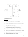
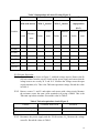
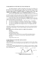
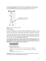
MEMORIAL UNIVERSITY OF NEWFOUNDLAND Faculty of Engineering and Applied Science Laboratory Manual for Eng. 3821 Circuit Analysis (2013) Instructor: E. W. Gill PREFACE The laboratory exercises in this manual have been designed to reinforce the concepts encountered in the course Eng. 3821, Circuit Analysis. They form a mandatory portion of the course, and while they are valued at 10% of the overall mark, unexcused, missed labs will result in an incomplete grade for the course. Official documentation, such as a doctor’s note in the case of illness, is required in order to be excused from graded work. Documented, valid reasons for missing graded work, including labs, will permit the transfer of the relevant marks to either the midterm or the final examination as agreed to by the instructor and the student. The specific objective of each experiment should be kept in mind throughout the laboratory session. The conclusions based on the experiments and other observed phenomena must be clearly discussed in the laboratory report. Before performing the experiments, the students must be aware of the basic safety rules for minimizing any potential dangers. Table of Contents Submission Format and Rules for Lab Reports….………………………. 2 Exp. 3821-1 Circuit Analysis Using PSpice.................................................. 6 Exp. 3821-2 Circuit Analysis for Resistive Circuits.................................... 9 Exp. 3821-3 The Oscilloscope and Function Generator.............................. 17 Exp. 3821-4 Step Response of RL, RC and RLC Circuits............................ 24 Exp. 3821-5 Sinusoidal Steady-State Response............................................ 28 Exp. 3821-6 Frequency Response and Resonance....................................... 33 Exp. 3821-7 Design of a Simple Filter......................................................... 37 REFERENCES 1. 2. 3. 4. Electric Circuits, 9 th Ed., W..Nilsson, S.A.Riedel, Pearson Education Inc., 2011. Introduction to PSpice Using OrCAD, J.W.Nilsson, S.A.Riedel, Pearson Education Inc., 2011. Introduction to Electrical Engineering Laboratories, E.B.Slutsky, D.W.Messaros, Prentice Hall, 1992. Fundamentals of Electric Circuits, 4 th Ed., C.K. Alexander, M.N.O. Sadiku, McGrawHill, 2009. Acknowledgements: Dr. B. Jeyasurya, Dr. J.E. Quaicoe, Mr. R. Hadidi, Ms. Eilnaz Pashapour 1 Submission Format and Rules for Lab Reports General: (1) Use a cover page as shown following these general instructions: (2) Start the Prelab immediately after the cover page. EACH PERSON in the group must submit a Prelab. Unless otherwise directed by the instructor, in order to obtain full marks for a lab report, the Prelabs for all but the first experiment must be shown to the lab Teaching Assistant before the lab starts unless otherwise indicated by the instructor for other specific labs. Failure to do so will result in a maximum grade of 7/10 for that lab. (3) The name of the person must be attached to the top of each Prelab. (4) Label the Prelab sections as they are in the online manual. (5) Use only one side of the paper in answering the Prelab questions as well as in the experimental write-up. (6) Start the actual lab write-up (one per group) after the last page of the Prelab. See the writeup requirements following the sample cover page in this document. Put the words “Lab Report” at the top margin of the first page of the actual write-up of the experiment. (7) Label the lab report sections as they appear in the online manual. (8) Staple the Cover Page, individual Prelabs, and a group Lab Write-up, in that order, together in a single package. (9) Graphs based on data collected in the lab may be produced manually or electronically (for example, using Microsoft Excel or any other convenient software). (10) Submission of each lab package is required at the start of the subsequent lab. The following three pages elaborate on some of the above points. 2 Sample Cover Page Faculty of Engineering and Applied Science Memorial University of Newfoundland Engineering 3821 Lab 3821-#X Title: Title of Lab as it Appears in the Online Manual Names: Name 1 and Student Number Name 2 and Student Number Date: Date that experiment was done 3 Lab Report Purpose: Restate the purpose of the lab as found in the online manual – feel free to use your own words. Apparatus and Materials: List in a column. Be sure to give the make and model of the apparatus if applicable. For example: (1) 1 EZ Digital Co., Ltd. Multimeter; Model: DM-441B (2) 1 GW INSTEK DC Power Supply; Model: GPS-3303 (3) Standard Resistors: 4.7 Ω, 18 Ω, 39 Ω (4) X sets of leads with banana plugs and alligator clips (5) Various connecting wires Theory: Give the equations used (along with the meanings of their symbols). For example: Ohm’s Law: The voltage (v), current (i) and resistance (R) either for a circuit element or the whole circuit are related as v=iR …. (1) …. and so on (for example, in Lab 2, you would also give the KVL, KCL and power formulae). Procedure: In general, you may simply say “As per lab manual”, but note any modifications that you make that may have enhanced the basic procedure. Label each part of the Experiment report according to the titles given in the manual. Part #: Title of this part. For example in Lab 2 you would have first Part 1 Node-Voltage and Mesh Current The first sub-heading should be: Data: Put the labelled circuit diagram (if relevant) at the beginning of this section. Under this sub-heading, also put (for example for lab 2): TABLE 1 – Verification of Kirchhoff’s Voltage Law (KVL) for Circuit of Figure 1 Carefully draw the table and fill it in with the measured or calculated values as required. Also, in the case where table entries require calculations, provide sample calculations below the table. That is, if there are several calculations which have exactly the same form, provide a 4 single sample. The other calculations will, of course, be completed and entered into the table, but there is no need to show many calculations which are identical in form. The next heading should be (as required) Questions, Discussion and Conclusion(s): Label these as suited. Repeat the above format for subsequent parts of the experiment. This general approach should be taken in all lab write-ups. It may vary slightly depending on the requirements. 5 Exp. 3821-1 Circuit Analysis Using PSpice PURPOSE 1. To learn the basic features of PSpice . 2. To use PSpice in studying: - Basic DC Analysis - Circuit Analysis involving Dependent Sources - Parameter interdependencies using Sweep Analysis INTRODUCTION The rapid change in the field of electrical engineering is paralleled by programs that use the computer’s increased capabilities in the solution of both traditional and novel problems. With the availability of tools for computer-aided circuit analysis, circuits of great complexity can be designed and analyzed within a shorter time and with less effort compared to the traditional methods. SPICE is a computer-aided simulation program that enables the design and simulation of circuits. SPICE is the acronym for a Simulation Program with Integrated Circuit Emphasis. It was developed at the University of California and made available to the public in 1975. OrCAD PSpice A/D from Cadence is a popular implementation for personal computers. For this course, we will use OrCAD PSpice Demo 16.2 or 16.3. In the following exercises you will use PSpice to solve some simple circuits and to determine several quantities of interest. PREPARATION (There is no Official Pre-lab to be completed and shown to the lab assistants prior to this Lab. However, some work as indicated immediately below should be done BEFORE the lab.) ● ● ● 1. Read Chapters 1, 2 and 3 of the manual, Introduction to PSpice Using OrCAD, by J. W. Nilsson and S. A. Riedel. Make a directory in your M: drive for all the PSpice files. Complete the following two problems: Solve the circuit of Figure 1 below using the Mesh Current method. (a) Determine the current magnitudes and indicate their directions for all branches of the circuit on the diagram submitted with your report. (b) Determine the voltage across all the elements (showing the correct polarities). (c) Check that your answers satisfy KCL at all nodes and KVL in all meshes. (d) Show that the power delivered by the sources equals the power absorbed. 6 Figure 1 2. Solve the circuit of Figure 2 below using the Node Voltage method. Notice that two of the essential nodes are labelled a and b. There are two other essential nodes. Label the one at the top of the 12 V source c and the remaining one d (where is it?). (a) Determine the current magnitudes and indicate their directions for all branches of the circuit on the diagram submitted with your report. (b) Determine the voltage across all the elements (polarity is important). (c) Check that your answers satisfy KCL at all nodes and KVL in all meshes. (d) Show that the power delivered by the sources equals the power absorbed. Figure 2 LAB SESSION The following instructions are meant to be supplemented by input from the lab teaching assistants. Be sure to save all files in your directory. Any of the following parts not completed during the lab period must be completed outside of lab hours. 7 Part 1. Carefully follow the step-by-step instructions in Chapter 1 of the PSpice manual – ensuring all Libraries (see Figure 5, page 4) have been added – and produce the circuit in Figure 11, page 9. ● Use ‘Place (from top line of toolbar) and then Net alias’ to specify node numbers, specifying the node between the 12 V source and the 3Ωk resistor as 1 and the node between the 3 kΩ and 6 kΩ resistors as 2 after you have drawn the circuit. Once you have placed the ground, which is essential to do as explained on pages 6 and 7 of the PSpice manual, it is specified automatically as node 0. If you don’t specify the other node numbers, they are specified automatically, with sometimes obscure grid numbers. It is usually a little easier to refer to node numbers which are user-specified. ● Simulate the circuit and determine all the voltages and currents. Note the V, I and W buttons on the toolbar which may be used to display voltages, currents and power associated with various parts of the circuit. ● Next place IPRINT,VPRINT1,VPRINT2 in suitable places in the circuit of Figure 11. (Refer to page 24 of the manual. Be careful with the polarities – they are incorrect in Figure 27.) Once you highlight a device, its polarity may be changed by right-clicking and choosing a `mirror horizontally’ feature etc., if necessary. ● Consider how the details in the output file (View Output file) relate to the node numbers, IPRINT, VPRINT etc.. ● Verify that the power output of the source equals the power consumed by the two resistors. Part 2. Construct and solve the circuit of Figure 1 above using PSpice. Be sure that you use the ‘ground’ and VPRINT/IPRINT parts where required here and elsewhere. Part 3. Construct and solve the circuit of Figure 2 above using PSpice. Part 4. Verify Example 1, page 18 of the PSpice manual – that is, use the PSpice software to repeat this example. Part 5. Construct and simulate the circuit of Figure 27 on page 23 of the PSpice manual. For source voltage varying from 0 volts to 100 volts in steps of 10 volts, determine the power absorbed by the 40 ohm resistor. Plot the variation of the power with the voltage on the x axis and the power on the y axis by appropriately using the Trace/Add Trace menu option as explained in the manual. REPORT Treat the PREPARATION section as a pre-lab. Each person in a group is required to submit the results from that section. Parts 1 to 5 of the LAB SESSION are to be submitted as a single submission per group attached to the PREPARATIONS from each student of the group. 8 Exp. 3821-2 Circuit Analysis for Resistive Circuits PURPOSE To understand and verify by experiment some of the basic techniques for the analysis of resistive circuits. INTRODUCTION This laboratory will be covered in two sessions, each of which must be submitted in the lab period one week after it is performed. Review the course notes and relevant text sections covering: (1) Kirchhoff’s current law (KCL) which describes current relations at any node in a lumped network (see page 6 of the text for the definition of a lumped-parameter network or system); (2) Kirchhoff’s voltage law (KVL) which describes the voltage relation in any closed path in a lumped network. (3) Node-Voltage and Mesh-Current methods of circuit analysis. (4) The principle of superposition. (5) Thévenin's theorem. (6) The maximum power transfer theorem which may be stated as: maximum power is obtained at a given pair of terminals when the terminals are loaded by the Thévenin resistance of the circuit. SESSION 1: Node-Voltage & Mesh-Current Methods PRELAB for Session 1 1. The circuit of Figure 1 contains two constant voltage sources. Solve this circuit using node-voltage method. Determine the currents through all the elements and voltages across all elements. Note carefully the direction of all currents and the polarity of all voltages. Verify that the total power developed equals the total power absorbed. Use Table 1 and Table 2 to record all your answers. 2. Repeat (a) using the mesh current method 3. Solve the circuit of Figure 1 using PSpice. Use part VPRINT1 and IPRINT (Page 24 of PSpice supplement) suitably. From the output file make a record of the required voltages and currents. (Be care with polarities.) 4. Repeat the PSpice simulation by considering the node ‘a’ in the Figure as the ground. Using the output file make a record of the required voltages and currents. 9 Figure 1 Circuit for Node-Voltage & Mesh-Current Methods LAB EXPERIMENT (Session 1) Before you start: The various functions of the Digital Multi Meter (DMM) and the power supply should be understood. Familiarization with the different ranges for measurement, purpose of the different control knobs, selector switches etc. is necessary. Consult the Lab Technologists or TAs for help as required. Note that the power supply has two variable and one fixed voltage output. The variable voltage outputs will be used for the experiments. It is a good practice to connect the ground of the power supply to the ground of your circuit. You should be familiar with the ‘color codes’ for the resistor. Refer to the ENGI 1040 Lab Manual or any convenient source. It is very important to use the correct value of resistance (verify using the color code and the DMM). For safety of the equipment and for personal safety follow the order of connecting and adjusting all devices and parts as specified. Also, be aware that resistors heat up over time and can be overly warm to touch. Care should be taken in this regard. 1.1. Construct the circuit in Figure 1 on the breadboard provided. Turn on the power supply and use the DMM to measure the source voltages. Within the limitations of the control knobs, ensure that the voltage sources are fixed at 20 V and 25 V after they are connected to the circuit by adjusting the power supply if necessary. 10 It is important to use the correct range of the DMM for the various measurements. 1.2. Measure the voltage across each resistor in the circuit with the polarity as indicated in Figure 1. Record these readings in Table 1. Table 1 Verification of Kirchhoff’s Voltage Law (KVL) Figure 1 Variable Calculated values from Prelab 1. Measured values VR1 (V) VR2 (V) VR3 (V) VR4 (V) VR5 (V) VR6 (V) VR7 (V) VR8 (V) 1.3. When you use the DMM as an ammeter, you have to disconnect some part of your circuit and connect the DMM in series with the element whose current you want to measure. Do this carefully. Before you make the connections, make sure that that the power supply is turned off. Measure the current flowing in each branch of the circuit with the direction as indicated in Figure 1. Record these readings in Table 2. 1.4. Table 2 Verification of Kirchhoff’s Current Law (KCL) Figure 1 Variable Calculated values from Prelab 1. Measured values I1 (mA) I2 (mA) I3 (mA) I4 (mA) I5 (mA) I6 (mA) I7 (mA) I8 (mA) 11 Lab Report (Session 1): Present all your results clearly. All the completed tables must be included in the report. All the calculations (both for the prelab and the experiment) must be shown clearly. 1.1 Based on the values in Table 1, determine the sum of measured voltages with proper sign around the closed paths adga, abga, acda, acba and bcdgb as in Figure 1. Verify that KVL is satisfied. 1.2 Based on values in Table 2, determine the sum of measured currents with proper direction at nodes a, b, c and d of Figure 1. Verify that KCL is satisfied. 1.3 Using the measured voltages and currents, determine the power associated with each element. Verify that the power delivered by the sources is equal to the power consumed by the resistors. 1.4 Compare the prelab values with the measured values. Show sample calculations of percentage errors for at least one current and voltage and discuss sources of error. 1.5 State appropriate conclusions based on the prelab and experiment and be sure to indicate how the selection of the ground node influences the final results. SESSION 2: Superposition, Thévenin Equivalent and Maximum Power Transfer PRELAB for Session 2 1. Solve the circuit of Figure 2 using the principle of superposition. That is, determine the currents through all the elements and voltages across all elements. Record the answers in Table 3. 2. Again, consider the circuit of Figure 2. Determine the Thévenin equivalent of the circuit with respect to the nodes a-b with the resistor R4 removed. Use this Thévenin equivalent circuit to determine the current through the resistor R4 and the voltage across it. Redraw the circuit using the Thévenin equivalent. Change R4 t o 1.5 kΩ and 2.2 kΩ and calculate the current through the resistor R4 and the voltage across it using Thévenin equivalent of the circuit. Record the calculated values in Tables 4 and 5. 3. Determine the value of a resistor RL to be connected between nodes a and b (Figure 2, without R4) so that it consumes the maximum power. Determine the maximum power delivered to the resistor RL. 4. Consider that RL varies from 100 Ω to 3000 Ω in steps of 10 ohms. Plot a graph of power versus resistance (i.e. resistor values on the x-axis and power on the yaxis). 12 Figure 2 Circuit for Superposition, Thévenin Equivalent and Maximum Power Transfer LAB EXPERIMENT (Session 2) 2.2 Superposition 2.2.1 Construct the circuit of Figure 2. Ensure that the voltage sources are exactly 20 V and 10 V after they are connected in the circuit using the DMM. 2.2.2. Measure the three currents in the circuit (note the direction) indicated in Figure 2. Record these reading in Table 3. 2.2.3 Measure the voltage across each resistor in the circuit with the polarity as shown in Figure 2. Record these reading in Table 3. 2.2.4 Turn off the power supply and remove V2 from the circuit. Replace it with a short circuit. Be careful not to short out the voltage source directly. Why? 2.2.5 Repeat the measurement of 2.2.2 and 2.2.3 and record the result in Table 3. 2.2.6 Turn off the power supply and return V2 to the circuit. Remove V1 from the circuit and replace it with a short circuit. Do not short out V1 directly. 2.2.7 Repeat the measurement of 2.2.2 and 2.2.3 and record the result in Table 3. 2.2.8 Complete the calculation indicated in Table 3 (column D) 13 Table 3 Superposition in Linear Circuits (Figure 2) A B C D Result by With both sources With V2 inactive With V1 inactive superposition (B+C) Variable Measure- Measure- Measure- MeasurePrelab Prelab ment Prelab ment Prelab ment ment I1 (mA) I2 (mA) I3 (mA) VR1 (V) VR2 (V) VR3 (V) VR4 (V) 2.3 Thévenin Equivalent 2.3.1 Connect the circuit shown in Figure 2 with both voltage sources. Remove the R4 (430 Ω ) resistor from the circuit. Switch on the power supply and ensure that the voltage sources are exactly 20 V and 10 V. Measure the voltage across the open circuit terminals (a-b). This is the Thévenin equivalent voltage. Record this value in Table 4. 2.3.2 Remove sources V1 and V2 and replace each source with a short circuit. Measure the resistance across the open circuit terminals (a-b) using a DMM. This is the Thévenin equivalent resistance. Record this value in Table 4. Table 4 Thévenin equivalent circuit (Figure 2) Variable Calculated from Prelab Measured Thévenin voltage Vth (V) Thévenin resistance Rth (Ω) 2.3.3 Reconnect the power supply and the 430-Ω resistor, R4. Measure the voltage across R4. Record the values in Table 5. 14 2.3.4 Repeat step 2.3.3 for R4 resistances of 1.5 kΩ and 2.2 kΩ. 2.3.5 Construct the Thévenin equivalent circuit. Adjust the source to the value of Vth determined in step 2.3.1. Use available resistors to form Rth by connecting them in series. Try to get the resistor as close to the as possible to Rth .Connect the 430 Ω resistor to the Thévenin equivalent circuit and measure the voltage across it. Record the values in Table 5. 2.3.6 Repeat step 3.5 for R4 resistances of 1.5kΩ and 2.2 kΩ. Table 5 Resistor R4 voltages (Figure 2) Resistor Voltage measured Voltage calculated Voltage masured in R4 in original circuit in Thevenin circuit Thevenin circuit 430 Ω 1.5 kΩ 2.2 kΩ 2.4 Maximum Power Transfer 2.4.1. For different values of resistances across terminals a-b, measure and record the voltage across and current through this resistor in Table 6. Use the circuit of Figure 2. 2.4.2. Repeat 4.1 with the Thévenin equivalent circuit. 2.4.3. Place the resistor that consumes the maximum power across terminal a-b (R*) (calculated from the Prelab). Measure and record the voltage and current in Table 6. Use the two different circuits as in 2.4.1 and 2.4.2. 2.4.4. Calculate the load power for each load using your measurements and record them in Table 6. 2.4.5. Plot the power consumed by the load resistor (both circuits) on the same graph as in prelab. 15 Table 6 Maximum power transfer (Figure 2) Load RL Measured load voltage Measured load current VL(V) IL(mA) Load Power P(W) Original Thevenin Original Thévenin Original Thévenin circuit circuit circuit circuit circuit circuit 100 Ω 430 Ω 2.2 kΩ 3.0 kΩ R*= Lab Report (Session 2): Present all your results clearly. All the completed tables must be included in the report. Samples of all the calculations (both for prelab and experiment) must be shown clearly. These should include relevant sample percent error calculations. 2.2.1. Compare the results obtained in Table 3. Does superposition hold for all the variables? Comment on any error. What are the principal sources of error in this experiment? 2.2.2 What are the challenges of using this method for a circuit containing many sources? 2.3.1 Discuss the results recorded in Table 4 and Table 5 and suggest possible applications? 2.4. Discuss possible applications of your discovery in Section 2.4. 16 Exp. 3821-3 The Oscilloscope and Function Generator PURPOSE - To learn how to use an oscilloscope to observe and measure both DC and AC voltages. - To generate AC (alternating current) and DC (direct current) signals using a function generator. - To build and analyze a DC and AC voltage divider circuit. - To construct and examine an RC circuit. - To become familiar with some features of the oscilloscope. EQUIPMENT • Tektronix Oscilloscope (TDS1000) • Function Generator (FG-7002C) • Multimeter Pre Lab. Tasks Study and understand Sections 9.1 and 10.3 of Text (Nilsson/Riedel) ● ● ● ● ● ● Draw two cycles of the voltage across a 60 Watts bulb at your home. Show clearly the time in x-axis and the magnitude in y-axis. Hint: What is the maximum voltage? Draw two cycles of the current through the 60 Watts bulb at your home. Show clearly the time in x-axis and the magnitude in y-axis. Draw two cycles of a square wave (frequency 1 kHz and 10 kHz on a different plot). Assume a 5 V amplitude. Draw two cycles of a triangular wave (Frequency 1 kHz and 10 kHz on a different plot). Assume a 5 V amplitude. Draw two cycles of a sinusoidal wave (Frequency 1 kHz and 10 kHz on a different plot). Assume a 5 V amplitude. Draw two cycles of a sinusoidal wave (Frequency 5 kHz). Assume a 10 V amplitude and a DC offset of 3 Volts. OVERVIEW In this experiment students are introduced to both the oscilloscope (scope) and function generator. The function generator creates a varying voltage source with different frequencies. The oscilloscope will be used to measure both the AC and DC components of a waveform. The oscilloscope is a voltage measuring device. The oscilloscope can be used to measure the amplitude of any waveform as well as the frequency and period of a periodic waveform. Before the actual experiment takes place, there are few familiarization exercises to be conducted. 17 FAMILIARIZATION WITH THE FUNCTION GENERATOR The function generator is capable of generating a wide variety of waveforms. For this session our focus will be on sine waves, square waves and triangle waves. Examine the front panel and record the features (different tasks that are possible) of the frequency range selector, the function switches, the frequency dial, the DC offset controls, and the amplitude control. Locate the main power switch for the device. The best way to understand the features of the function generator is to observe the waveforms using the oscilloscope (at this point note Figure 1 and related text). You will do more experiments using the oscilloscope in the second section. For the present, we will use the oscilloscope to observe some signals from the function generator. Connect the output of the function generator to Channel 1 of the oscilloscope. Adjust the function generator and observe the following waveforms. Make a rough sketch of the waveforms. Refer to your pre lab tasks. ● Two cycles of a square wave (Frequency 1 kHz and 10 kHz), 5 V amplitude. ● Two cycles of a triangular wave (Frequency 1 kHz and 10 kHz), 5 V amplitude. ● Two cycles of a sinusoidal wave (Frequency 1 kHz and 10 kHz), 5 V amplitude. ● Two cycles of a sinusoidal wave (Frequency 5 kHz), 10 V amplitude and a DC offset of 3 Volts. Adjust some control knobs on the function generator, observe the waveforms and make a record of your understanding. Can you relate the displays at the bottom of the screen to your signal? Basic features of the oscilloscope required to complete this experiment: Measure CH1 Menu Vertical Position Control Horizontal Position Control 5 buttons close to the screen; these are very useful for measuring frequency, amplitude etc.. You may have to use the ‘Back’ option button (5th button) frequently. Trigger Menu/ Source/ CH1 FAMILIARIZATION WITH THE OSCILLOSCOPE Oscilloscope Probes - The oscilloscopes used in this laboratory have been designed to measure node voltages. Therefore, one end of the oscilloscope probe (long lead) has to be connected to the ground terminal. - For the “hot” terminal of the probe always use a “hook-up” wire to measure a voltage. Do not attach the “hot” terminal directly to a circuit component and never take the plastic sleeve off the probe. (See Figure 1.) Figure 1 The Oscilloscope probe. 18 How the Oscilloscope Works Most of the oscilloscope screens are similar to a television screen (see Figure 2). The inside is coated with phosphor which glows when struck by an electron beam. But, the scope we use in this lab is digital and uses an LCD instead. A signal to be viewed is put into an amplifier which deflects (moves) the beam position vertically (up and down). The deflection can be time-varying (AC signal) or constant (DC signal). Signals displayed on the screen can be measured numerically by counting grid divisions printed on the screen, and multiplying by the amplifier settings on the control knobs. Figure 2 The oscilloscope display: there are 10 horizontal divisions and 8 vertical divisions. Familiarize yourself with the different functions of the 5 buttons close to the screen; these are very useful for measuring frequency, amplitude etc.. You may have to use the ‘Back’ option button (5th button) frequently. The vertical and horizontal controls are briefly discussed below (see Figures 3 and 4). This knob adjusts the vertical zero position Number of volts per vertical screen division is set with this knob. Figure 3 Main controls for the vertical amplifier: the number of volts per division and the zero reference are set here. 19 In order to display a signal as a function of time, an internal time-base generator (also called a sweep generator) is used to sweep the beam horizontally at a rate selected on the front panel. This turns the horizontal axis of the display into a "time axis." The number of seconds per Horizontal division is set Figure 4 Time-base generator controls. EXPERIMENTS On the breadboard there are is a power supply with connectors for positive (+) and negative (-) voltages and a common return. In the available connectors this common return will be connected to an actual ground within the supply. Although you cannot see it, the oscilloscope and signal generator instruments also have one lead connected to this ground. In this and future exercises, be particularly careful when placing wires near any power contacts. The power supplies and the signal generator can be easily destroyed by incorrect connections. Leave the breadboard power off. Use the following experiments and gain an understanding of the different features of the oscilloscope. These will be useful whenever you use this oscilloscope. It is suggested that you keep a Journal and record all the steps carefully. You can use this Journal as a ‘Users’ manual’ for this oscilloscope. Basic Features Repeated Measure CH1 and CH2 Menu Vertical Position Control Horizontal Position Control 5 buttons close to the screen; these are very useful to measure frequency, amplitude etc. You may have to use the ‘Back’ option button ( 5th button) frequently. Trigger Menu/ Source/ CH1 or CH2 Measurements: Some of the possible measurements that will be useful are: Frequency, period, Mean, Peak-Peak, RMS, Minimum and Maximum. 20 Cursors: The cursors always appear in pairs and allow measurements to be taken by reading their values from the display readouts. There are two types of cursors: Voltage and Time. To use cursors, push the CURSOR button and set the source to the waveform on the display that you want to measure. Voltage Cursors: Voltage cursors appear as horizontal lines on the display and measure vertical parameters. Time cursors: Time cursors appear as vertical lines on the display and measure the horizontal parameters. 1. DC voltage from the bread board: 1.1 Connect the fixed 5 V supply to Channel 1. Measure this voltage using the oscilloscope and multimeter. Connect the variable (positive) supply to Channel 1. Adjust for +6 V and then for +16 V. Measure these voltages using the oscilloscope and multimeter. Change the attenuation switch in the probe to 10X. Measure +12 V. Investigate the function of the ‘probe’ option in the oscilloscope and note your observations. Connect the variable (negative) supply to Channel 1. Adjust for -6 V and then for -16 V. Measure these voltages using the oscilloscope and multimeter. 1.2 1.3 1.4 2. DC Voltage Divider 2.1 Build the simple circuit shown in Figure 5 and apply 10 V DC from the power supply to the circuit, and then measure the amplitude of the signals at A and B with respect to ground. VA is the source voltage and VB is the voltage across the 150 K resistor. Probe A 100K Power Supply 10V DC Probe B 150K Probe Ground Figure 5 The DC voltage divider. 2.2 2.3 Use the dual mode in your oscilloscope to display both signal A and B. Your oscilloscope has a math function; by selecting it you can get VA – VB and VA + VB. Measure the amplitude of this signal and verify that it is as expected. 2.4 Calculate the ratio VB/VA. Does the answer match with what you expect based on your understanding of basic circuit concepts (i.e. the voltage divider rule)? 21 3. AC Voltage Divider In the circuit of experiment 2 change the source voltage to AC sinusoidal voltage with frequency of 1 KHz and peak to peak amplitude of 10 V (see Figure 6). 3.1 Measure the amplitude of the signals at A and B with respect to ground. Probe A Probe B 100K Power Supply 10V P-P AC f=1KHz 150K Probe Ground Figure 6 The AC voltage divider. P-P means positive peak to negative peak. 3.2 3.3 Repeat parts 2.2 to 2.4 for the above circuit. Use the multimeter to measure all these three voltages and compare your oscilloscope and meter readings. Note: The meters read rms (root mean square – see text) values for a.c. signals. 4. RC Circuit and Phasor Measurements 4.1. Build the RC circuit as shown below, using R = 100 kΩ and C = 1nF. Probe A 100K Power Supply 10V P-P AC f=1KHz Probe B 1nF Probe Ground Figure 7 A simple RC Circuit. 22 4.1.1 Display the source voltage and the voltage across the capacitor. Note the phase of the capacitor voltage (in degrees) with respect to the source voltage. Note the peak values of these voltages. 4.1.2 Use the dual mode in your oscilloscope to get the voltage across the resistor using the suitable ‘Math’ function of the oscilloscope. Note the phase of the voltage (in degrees) across the resistor with respect to the source voltage. Note the peak value of this voltage. 4.1.3 Make a rough plot of these voltages (2 cycles); show the quantities of interest. It is necessary to use the ‘Math’ function of the oscilloscope here. Since this measurement can be challenging at first, please get help from the TAs or Professor. When you measure the phase difference, note which signal is lagging (or leading). The analysis of this type of circuit will be discussed in the class. 4.1.4 Measure the voltages VA and VB using multimeter and record the values. 4.1.5 Verify if KVL is satisfied in the circuit based on the measured values. Discuss your answer. 4.2 Change the source frequency to 10 kHz. 4.2.1-4.2.5 Repeat all the measurements of 4.1.1 to 4.1.5. Compare and discuss. You may find this lab a little challenging, but it should prove very useful in later experiments. REPORT Submit a detailed record of all the procedures and results in this lab session. References: 1. 2. FG-7002C Sweep Function Generator Operation Manual, EZ Digital Co., Ltd. TDS1000- and TDS2000-Series Digital Storage Oscilloscope User Manual, Tektronix, Inc. 23 Exp. 3821-4 Step Response of RL, RC and RLC Circuits PURPOSE 1. To study the response of RC, RL and RLC circuits when energized by an independent voltage source. INTRODUCTION Many phenomena that occur in electric circuits involve or produce time-dependent variables. When a RC, RL, or RLC circuit is suddenly energized or de-energized, a transient phenomenon occurs which dies out as the circuit approaches the steady-state operation, occurs. This is because of the way in which inductors and capacitors store energy and resistors dissipate the energy. The nature of the transients depends on the values of R, L and C as well as on how they are combined in a circuit. The steady state response of the circuit, which is determined by the external source, is reached only after a transient time interval. As discussed in the class, the response of RLC circuits may be classified as under damped, critically damped or over damped. PRELAB 1. Refer to Chapter 6 and 7 of the PSpice supplement. This will be useful for your prelab study. 2. The circuit of Figure 1 is excited by a square wave voltage of 4 V (peak or zero to peak) having a frequency of 100 Hz. In PSpice, use VPULSE to create this voltage waveform by setting V1 to 0 and V2 to 4. For additional information on ‘pulse’ waveform, refer to page 100 and 101 of PSpice supplement. Use a pulse width of 5 ms. (What is the pulse period here?) Use PSpice to determine the transient response (voltage across the capacitor) of the circuit. Limit your transient response plot to one cycle of the source voltage. This may be done by setting the "Run to time" parameter in the "Edit Simulation" window to be of the same length as the period of the VPULSE. Obtain the response for the following two RC combinations: R=3.3 kΩ ; C=0.1 μF; R=3.3 kΩ ; C=0.22 μF Calculate the time constants using the circuit parameters. Also, determine them from the plots. Remember the response changes by a factor of 1/e during one time constant. Figure 1 RC circuit with square wave input. 24 3. The circuit of Figure 2 is excited by a square wave voltage of 4 V, zero to peak as before, but now with a frequency of 5 kHz. Again, create the waveform so that the pulse width is half the period. Use PSpice to determine the step response (voltage across the resistor) of the circuit. Limit your transient response plot to one cycle of the source voltage. Obtain the response for the following two RL combinations (simply change R and repeat): R=100 Ω ; L=1.0 mH; R=220 Ω ; L=1.0 mH L 2 1 V1 R Figure 2 RL circuit with square wave input. 4. The circuit of Figure 3 is excited by a square wave voltage of 4 V as before, but with a frequency of 500 Hz. Using Pspice obtains the plot of the variation of the voltage across the capacitor. Assume zero initial conditions. Limit the response to two cycles only. Do your simulations for the following two combinations. R = 1.5 Ω, L = 2.2 mH, C= 0.1 μF; R = 68 Ω, L = 2.2 mH, C = 0.1 μF; R L 1 2 C V Figure 3 RLC circuit with square wave input. Find the frequency of the oscillations using the circuit parameters. Also, determine them from the plot. Note that, theoretically, this frequency (in radians/second) is given by = ωd 1 R − LC 2 L 2 25 EXPERIMENT Note: There may be minor differences in the components you use in the experiment and those you have used for prelab. Preliminaries: Setting up the Equipment Note: Follow the steps in the experiment on the oscilloscope to take the required readings. For example, the cursor feature will be useful for voltage and time measurements. Set the controls on the function generator to output a square wave with an amplitude of 4 V and a frequency of 100 Hz. Connect the output of the function generator to channel 1 of the scope. Use the time base and amplitude controls to adjust the scope display. Likewise the vertical and horizontal positioning may be adjusted to move the curve. Be sure to check the ground level of the scope to make sure amplitude measurements are accurate. 1.1 Construct the circuit of Figure 1. Adjust the function generator to provide a 4 V (peak), 100 Hz symmetrical square wave. Note that the use of this signal enables you to simulate the effect of repeatedly energizing the RC circuit and the waveform in the oscilloscope may be considered similar to the step response of this circuit. Sketch to scale the first half of the input square wave and voltage across the capacitor. Determine the time constant of the circuit by observing the waveform. Repeat the measurement for the second half of the input signal. Do your experiment for the following two combinations: R = 3.3 kΩ ; C = 0.1μF; R = 3.3 kΩ ; C = 0.22 μF Make sure that the function generator provides a 4 V (peak) 100 Hz symmetrical square wave with all elements connected. 2.1 Construct the circuit of Figure 2. Adjust the function generator to provide a 4 V (peak), 5 kHz symmetrical square wave. Sketch to scale the first half of the input square wave and the voltage across the resistor. You may have trouble getting the wave to look exactly square – why is this the case in the experiment when it wasn’t the case in PSpice? Determine the time constant of the circuit. Carry out the experiment for the two combinations of R and L as in the prelab. Be sure that the function generator provides a 4 V (peak) square wave with all elements connected. 3.1 Construct the circuit of Figure 3. Adjust the function generator to provide a 4 V (peak), 500 Hz symmetrical square wave after connecting all the elements. Note that the use of this signal enables you to simulate the effect of repeatedly energizing the RLC circuit and the waveform in the oscilloscope may be considered similar to the step response of this circuit. Sketch to scale one half of the input square wave and the voltage across the capacitor. Complete the 26 experiment for the two combinations of the circuit elements as in prelab. For the response which is more oscillatory, try to estimate the frequency of oscillation. REPORT: 1. Based on your experiments with the two RC circuits, discuss the effect of changing R and C on the nature of the response and final value of the capacitor voltage. Compare the experimental plot with that obtained using PSpice (PreLab) and comment on the discrepancies. 2. For the experiment with the RL circuits, discuss the effect of changing R and L on the nature of the response, final value of the resistor voltage and final value of the current in the circuit. Compare the experimentally determined time constant with that obtained using PSpice (Prelab) and comment on the discrepancies. 3. Compare the response of the RLC circuits obtained from the experiment with the PSpice simulation. Discuss the differences between the types of response for the two circuits. Compare the experimentally determined frequency of oscillation with the theoretical value. 27 Exp. 3821-5 Sinusoidal Steady State Response PURPOSE 1 To examine phasor analysis in PSpice. 2. To determine the steady state response of RLC circuits using phasors. 3. To study complex impedance matching and maximum power transfer for a general ac circuit. INTRODUCTION The bulk of the electric power generated in power plants throughout the world and distributed to the consumers appears in the form of sinusoidal variation of voltage and current. The analysis of many circuits and devices is accomplished by the techniques embodied in the sinusoidal theory. The sinusoidal steady state response of circuits can be described using the concept of phasors. Phasors may be represented in polar form as a magnitude and phase or equivalently in complex form (i.e. the sum of real and imaginary parts). PRELAB Here PSpice will be used to perform phasor analysis on ac circuits operating in steady state. The first part of the Prelab is a tutorial that will provide a familiarization with some of the basic PSpice features necessary for such an analysis. Refer to Chapter 10 of the PSpice supplement to understand ‘Sinusoidal Steady-State Analysis’ in PSpice. Prelab Part 1 In PSpice, construct the circuit shown in Figure 1. The necessary steps are outlined below and some of the important screens that will be encountered are shown in Figure 2. • • • • In the analog library parts list choose the resistors and inductor as required. From the SOURCE library choose VSRC and set the ac value to 6. The "Tran" and "dc" values may be ignored or deleted. Install the ground as usual. From the SPECIAL library choose and install the "PRINT1" parts at nodes 1, 2, and 3 (these nodes should be labelled using the "Place>Net Alias" feature. Double click on each of these parts and (for node 1) set the "ANALYSIS" field to ‘ac v(1) vp(1)’ where the three arguments together indicate that PSpice will return the magnitude and phase of the ac voltage of that node relative to ground. See Figure 2a. Repeat these labels for the PRINT1 devices at nodes 2 and 3. 28 R1 100 1 2 1 L1 2.2mH 2 3 V1 AC = 6 R2 150 Figure 1 Circuit for Part 1 of Prelab Indicate Magnitude Y and Phase Y in this screen. (a) (b) Figure 2 Screens for Part 1 of Prelab (a) Setting the PRINT 1 "ANALYSIS" field; (b) Simulation Profile. 29 • From the "PSpice>New Simulation Profile" choose "AC Sweep" and set the AC Sweep Type to "Linear", the "Start Frequency" and "End Frequency" to 15000 and the "Total Points" to 1 as shown in Figure 2(b). • The PRINT1 devices put their output in the file which may be viewed from the "PSpice>View Output File" menu option. In the above circuit, the PRINT 1 has been used to establish voltage magnitude and phase. It could also be used to find currents. For example, setting "ANALYSIS" value of Figure 2(a) to ‘ac I(R_R1) Ip(R_R1)’ would give the magnitude and phase of the current through resistor R1. • To determine the voltage across a device using the PRINT1 values in the Output File, the individual voltage on either node of the device must be subtracted. For example, the voltage across the inductor in Figure 1 is V2 - V3. These voltages are phasors. Convert the three voltages in the output file to complex numbers and show that Kirchhoff's voltage law holds for the circuit. Prelab Part 2 Solve the circuit of Figure 3 and determine the phasor voltages V1, V20, V23, V30, V24 and V40. Use the source voltage as the reference phasor. The ac voltage source is 6 V (peak). Use PSpice to verify your answers. This is just the previous circuit with another branch added. Note the node numbers. Ignore the terminal numbers (2 1 for L1) of the inductor. Figure 3 Circuit for Part 2 of PreLab Prelab Part 3 • Figure 4 may be considered as a circuit having a fixed load connected between terminals a and b, but variable source impedance. The load consists of resistor R2 and inductor L1 while the “source impedance” is changed by varying the capacitor values. Determine the value of the capacitor for which maximum power is transferred to the load when the source voltage is 6 V (peak) and has a frequency of 15 kHz. • Determine the value of the capacitance C1 so that the overall power factor of the circuit is unity at the frequency of 15 kHz. 30 R1 C1 120 R2 V2 120 AC = 6 2 L1 2.2mH 1 Figure 4 Circuit for Part 3 of Prelab EXPERIMENT Refer to your notes on the use of the oscilloscope. The cursor feature, Math Function (CH1-CH2) etc. will be useful for these experiments. 1.1 Build the circuit of Figure 3 and measure the following phasor voltages at 15 kHz with the oscilloscope. Measure the phase relative to the input signal from the function generator. (If required, seek help in making the phase measurements with the scope). Compare the results of your measurement with prelab simulation and with the hand calculations. Enter your experimental readings in the following table. Phasor Prelab Calculation Prelab: Pspice Experiment V1 Mag: 6; Angle: 0 Mag: 6; Angle: 0 Mag: 6; Angle: 0 V20 V23 V30 V24 V40 2.1 Build the circuit of Figure 4. Operate the circuit at a frequency of 15 kHz. Use each of the following values for C: 0.025, 0.047, 0.068, 0.10 and 0.22 microfarads (or whatever is available in the lab). Make sure that the input voltage remains constant throughout the experiment – adjust it if it does not (why might the source voltage change?). Make R2 = 100 Ω instead of 120 Ω (Why? Hint: Is the inductor ideal?). Using a DMM, measure the current in the circuit. Using the current measurements, plot the power consumed by the load resistor R2 as a function of capacitance. Comment on the results. 31 REPORT: Present all results (including Prelab tasks) clearly. Show all calculations and comment on all significant results. Phasor diagrams are important for this Lab. Using your measurements, as well as Prelab calculations, verify that KVL is satisfied in the loop containing L1, C1, R2 and R3 (Figure 3). Prove this using a phasor diagram. Comment on any discrepancies between simulations or hand calculations and what were measured in the lab. 32 Exp. 3821-6 Frequency Response & Resonance PURPOSE 1. To determine the frequency response of RC and RLC circuits. 2. To study resonance is a series RLC circuit excited by a sinusoidal source. INTRODUCTION The current and voltage responses in circuits containing inductors and capacitors (besides resistors) are frequency-dependent because the impedances of the former elements vary with frequency. Such circuits can be therefore used as "frequency-selective circuits" or filters - that is, they respond to signals of different frequencies differently and can therefore be designed to "pass" certain frequencies to a load or other parts of the circuit and to attenuate others. The study of the frequency response of a network involves the consideration of the magnitude and phase of the steady state voltages and currents as the frequency varies. An integral part of such a study involves the concept of resonance - a condition in which a circuit response can be maximized by adjusting either the circuit elements or the frequency of operation. THEORY The resonant frequency, ω0, of an RLC is given by 1 ……(1) ω0 = LC The half-power frequencies – i.e. the frequencies at which the power associated with the output signal drops to one-half of its maximum value – for a series RLC circuit (in this lab the output signal is a voltage signal taken across R) are given by (see diagram at end of this lab) ω1 = − R R2 1 ……(2) + + 2 2L LC 4L R R2 1 ..……(3) + + 2 2L LC 4L The half-power bandwidth is given simply by ω2 = BW = ω2- ω1 = R/L ……(4) 33 PRELAB General Guidelines: Draw schematics for the circuits indicated in Figures 1a and 2. Use source VSRC, AC = 1. Since vin = 1, vo itself will give the desired response. Some of the PSpice parameters are shown on the diagram. Setup: AC Sweep, Linear and specify the frequency range as shown in Figure 1b. Refer to the PSpice Supplement. 1. Let the circuit of Figure 1a be excited by a sinusoidal source whose frequency varies from 10Hz to 40 kHz. Use PSpice to obtain a plot of | vo/vin| versus frequency. In Probe, set the x axis setting of the plot to log scale. R1 1 kΩ 2 V1 0.1uF vin C1 v0 AC = 1V Figure 1a. RC Circuit Figure 1b. PSpice "simulation profile" for frequency sweeping. 2. Consider the circuit of Figure 2. Let the circuit be excited by a sinusoidal source whose frequency can be varied from 100 Hz to 100 KHz. Use PSpice to obtain a plot of | v0/vin | versus frequency for two different values of R1 (47Ω and 220 Ω). Obtain the two required plots on the same graph (by creating two circuits in the same Schematics file). In Probe, set the x axis setting of the plot to log scale. L1 1 1mH vin C1 2 0.47u V01 V1 R1 AC = 1V v0 Figure 2 RLC Series Circuit. 34 3. Calculate the resonant frequency and half-power frequencies of the circuit in Figure 3. Draw a phasor diagram (i.e. for the voltage across all elements at the resonant frequency). DMM 0.47µF vin 1.0 mH 1 2 47Ω Figure 3 Circuit for Part 3 of Prelab and Lab. EXPERIMENT Refer to your notes on the Oscilloscope and use the relevant features for these experiments. 1.1 Connect the circuit of Figure 1. Adjust the function generator to provide 3 V (6V peak-peak) supply. For the source frequency varying from 60Hz to 20kHz, measure v0 and vin for 12 different frequencies. Use the oscilloscope or counter to measure the frequency accurately. 2.1 Experimentally determine | v0/vin | as a function of frequency for the circuit of Figure 2 for values of R1 equal to 47 Ω . Take more readings near the frequency of interest. Use the DMM. 3.1 For the circuit of Figure 3, apply a 3 V (6V peak-peak) sinusoidal source. Vary the source frequency and experimentally determine the resonant frequency and halfpower frequencies. Use the DMM to measure the current. Carefully note the point of resonance and measure the magnitude and phase of all voltages (source & across all circuit elements) at resonance using the oscilloscope. For phasor measurements, you may have to follow the procedures of Lab. 5. Make sure that the source voltage is kept constant. REPORT: Plots: Since the range of the x axis is large, plot using a semi-log graph. 1. Draw the frequency response of the RC circuit using your measurements. From your plot, determine the half-power frequency and compare it with the theoretical value. Compare the experimental plot with that obtained using PSpice. Suggest a possible application of this circuit. 2. Draw the frequency response for the series RLC circuit. Compare this plot with the plot obtained by the PSpice simulation. Discuss the influence of the value of the 35 resistance in the frequency response of the circuit. Suggest an application for this circuit. 3. Compare the resonant frequency and bandwidth of the circuit based on your experiment with that of the Prelab. Compare the calculated and measured voltage phasors at resonance. Discuss the nature of the circuit at resonance using a suitable phasor diagram based on your experiment. 4. Discuss your understanding of the frequency response of the different circuits you have used in this laboratory session. Resonance Curve (For RLC Series Circuit) Current, i (A) im im/û 2 Ô1 Ô0 Ô2 Angular Frequency, Ô (rad/s) 36 Exp. 3821-7 Design of a Simple Filter PURPOSE 1. To design a filter to pass a signal at a desired frequency and reject the signal at another frequency. 2. To simulate this circuit in PSpice and study its frequency response. 3. To experimentally verify the performance of the filter. INTRODUCTION A filter is a frequency-selective device which allows certain frequencies to pass through it while blocking or severely limiting others. It is possible to design simple circuits using resistance, inductance and capacitance which act as filters. Here a study the frequency response of a particular RLC circuit configuration is examined. PRELAB 1. Consider the circuit of Figure 1. The circuit capacitors C1 and C2 are to be chosen so that the circuit effectively transmits a 25-kHz signal and effectively blocks a 50-kHz signal. • Calculate C2: The L1 and C2 parallel combination should be an open circuit at 50 kHz (i.e. choose C2 so that the impedance of the parallel combination is infinite). • 2. Calculate C1: Use the value of C2 determined above and minimize the overall impedance of the circuit at 25 kHz. In PSpice, simulate the circuit of Figure 1 using a sinusoidal source (VSRC with AC=1) whose frequency varies from 10kHz to 60 kHz. The simulation should be set up to do an AC sweep. Obtain a decibel plot of |V0/Vin| (see Figure 2). Use the 'cursor' features of PSpice to show the response of this circuit at the frequencies of interest. 37 L1 1 C1 ? 1 2 2mH C2 ? Vin AC = 1 2 R1 820 Figure 1 Frequency-Selective Circuit Figure 2 Obtaining a decibel plot of the output/input magnitude ratio in PSpice. EXPERIMENT 1. Construct the circuit of Figure 1. Use the components based on the Prelab. Adjust the input for 5 V (peak; or 10 V peak to peak) sinusoidal. For the source frequency varying from 10kHz to 60 kHz, measure V0 and Vin for 20 different frequencies using Oscilloscope. In particular, carefully record the output voltages near the frequencies of interest (20 kHz and 50 kHz). REPORT 1. Plot the frequency response of the circuit you have designed based on your measurements. Use Excel (or some other convenient software) to obtain the plot. Compare the experimental plot with that obtained using PSpice. Discuss your results. NOTE: Prelab and Lab Report must be submitted at the end of the Lab Session. 38