1
Lesson 16
Analog-to-Digital Converter (ADC)
1.
Overview
In this lesson, the Analog-to-Digital Converter (ADC) of the Cortex-M3 is introduced. For detailed description
of the features and controlling options for the ADC, read chapter 29 of the LPC17xx User Manual.
2.
Background
Most signals in the world exist as continuous functions of time in an analog format (e.g. voltage, current, speed,
force, pressure, temperature, sound, colors, etc.) In order to use these signals in the digital domain (store,
manipulate/edit), we must approximate the digital (binary) representations of these signals in a discrete fashion.
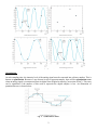
For example, an overview of the ADC process to convert an analog audio signal to digital format is shown in
the figure below.
Fig. 1 Overview of the ADC process (from EE334 Thinking Digital Lesson)
A digital representation of the signal can be easily stored, manipulated (edited), transmitted, etc. When an ADC
process is utilized, two things need to be considered to convert an analog signal into a digital format:
Sampling rate: this rate would determine how often we need to record a sample value from the analog
signal.
Quantization: how to divide the analog range into discrete, measured portions. The number of
quantization levels would determine the number bits that are required to represent each sample of the
signal.
Sampling rate:
The sampling rate is dictated by the highest frequency component of the analog signal. The sampling rate
suggested by the Nyquist Theorem which states that if a signal is sampled with a frequency of Fs, then the
digital samples only contain the frequency components form 0 to ½ Fs. In other words,
𝐹𝑠 ≥ 2(𝐹𝑚𝑎𝑥 )
Where Fs is the sampling frequency and Fmax is the highest frequency component of the analog signal. If the
sampling rate is too slow (Fs <2 Fmax), aliasing error can occur. Aliasing is when the digital signal appears to
have different frequency than the original analog signal. For example, consider the 7 KHz analog signal below.
If the sample rate is 10 KHz (<2 Fmax or 14 KHz), the analog values would be sampled every 100us (1/10 KHz)
as shown. Now if we only consider the sample points and try to recreate the analog signals form these samples,
we could end up with a 3 KHz signal instead of the original 7 KHz signal.
1
Fig. 2. Illustration of sampling and alias in the ADC process.
Quantization:
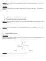
At each sampling time, the intensity level of the analog signal must be converted into a binary number. This is
known as quantization. Because we use discrete levels to represent samples, there will be quantization error
when an analog signal is reconstructed from its digital form (Digital-to-Analog Conversion or DAC). This error
can be significant if the number of bits used to represent the digital samples is low. An illustration of
quantization error is shown below.
Fig. 3. Quantization error.
2
Question: What would be the reconstructed signal of the original 7 KHz analog signal in Fig. 1 if 1 bit is used
for quantization?
Resolution:
Resolution is the smallest unit of intensity (voltage) that the ADC process can resolve. The resolution is
defined as
𝑉𝑚𝑎𝑥 − 𝑉𝑚𝑖𝑛
𝑉𝑚𝑎𝑥 − 𝑉𝑚𝑖𝑛
=
𝑛𝑢𝑚𝑏𝑒𝑟 𝑜𝑓 𝑞𝑢𝑎𝑛𝑡𝑖𝑧𝑎𝑡𝑖𝑜𝑛 𝑙𝑒𝑣𝑒𝑙𝑠
2𝑁
𝑟𝑒𝑠𝑜𝑙𝑢𝑡𝑖𝑜𝑛 = 𝑞 =
where
Vmax is the maximum voltage allowed in the analog signal.
Vmin is the minimum voltage allowed in the analog signal.
N is the number of bits used in the ADC process voltage.
Question: What is the resolution of the ADC if 1 bit is used to represent sample values of the original 7 KHz
analog signal in Fig. 1?
𝑞 ==
1 − (−1)
= 1𝑉
21
Question: What is the resolution of the ADC for analog signal shown in Fig. 3? Assume that Vmax=1V, Vmin=0V
𝑞 ==
3.
1 − (0)
= 0.125𝑉
23
Analog-to-Digital Converter
ADC Circuit:
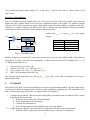
There are several types of circuits that can do ADC. The simplest circuit is to use an opamp comparator. An
example of which is shown in Fig. 4.
Fig. 4. 1-bit ADC circuit (from EE334 ADC Lesson).
Question: When will the opamp in Fig. 4 have an output of 5V, 0V?
Vout = 5V whenVin > VREF
3
Vout = 0V whenVin ≤VREF
If we consider the opamp output voltage of 5V as bit value ‘1’ and 0V as bit value ‘0’, then we have a 1-bit
ADC circuit.
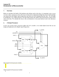
Successive Approximation:
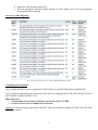
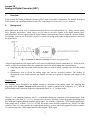
Now, let’s consider the block diagram below for a 2-bit ADC circuit. The control logic block sets or clears the
output bits (ADC outputs) based on the successive comparison results of the opamp. The Digital-to-Analog
Converter (DAC) below generates an output voltage based on the 2-bit input number. A summary of the DAC
voltage (VDAC) output is shown in the table below. DAC is another topic that should be discussed in another
lesson. In this lesson, we will focus on the analog-to-digital conversion.
Vin
+
Vout
-
Assume that Vmax = 5V and Vmin = 0V. DAC output
voltage:
Control Logic &
Register
Input D1D0
112
102
012
002
D1
D0
VDAC
DAC
Output VDAC (V)
Fig. 4. 2-bit ADC circuit.
Initially, all the bits are cleared. The control logic sets one bit every clock cycle (MSB to LSB). If the output of
the opamp is 5V (logic 1), the bit is left unchanged as 1, otherwise the bit is cleared. For example, let Vin = 3.15
V, find the digital value for Vin.
i.
ii.
iii.
iv.
First, clear D1D0. So, D1D0 = 002
Set bit D1. So, D1D0 = 102. Therefore, VDAC = 2.50V. Since Vin > 2.50 V, the bit is left unchanged.
Next, set bit D0. So, D1D0 = 112. Therefore, VDAC = 3.75V. Since Vin < 3.75 V, bit D0is cleared.
Done. The final output of the ADC is 102.
The same idea can be repeated for an N-bit (DN-1DN-2 …D1D0) ADC circuit. This is an example of a successive
approximation ADC.
4.
LP1768 ADC
The built-in 12-bit ADC of our microcontroller uses successive approximation method. The input signal can be
selected from 8 different channels (pins). Similar to other peripherals, controlling the ADC operation will be
done via the memory-mapped registers. Two major tasks to be completed:
i.
ii.
Configure the peripheral: This task requires setting all the associated options to enable the ADC system.
Sub-tasks in this step includes:
a. Enable the power to the ADC (default disabled).
b. Select the appropriate clock frequency
c. Configure the associated pin
d. Select the operation mode and configure other conversion options
Enable interrupt: This task is not required for all application. Sub-tasks in this step includes:
a. Enable the ADC to generate an interrupt request when a conversion is completed.
4
b. Enable the ADC interrupt in the NVIC
c. Write the appropriate interrupt handler function for ADC. Make sure to clear the appropriate
interrupt flag before returning.
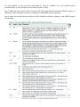
Overview of ADC Registers:
From Table 530 in the LPC17xx User manual, NXP Semiconductors, 2010.
Configuring the Peripheral:
Step 1: Enable the ADC power by setting the PCADC bit (bit 12) of the PCONP register (0x400FC0C4).
Step 2: Select the appropriate clock frequency for the ADC by configuring the PCLK_ADC bits (bits 25:24) of
the PCLKSEL0 register (0x400FC1A8).
Important notes:
The maximum clock frequency allowed to operate the ADC is 13 MHz.
It takes 65 clock cycles to complete one conversion.
Question: to ensure the proper operation of the ADC, what value should be assigned to PCLK_ADC bits in the
PCLKSEL0 register?
PCLK_ADC bits = bits (25:24) = 112
Setting PCLK_ADC = CCLK/8 = 100 MHz/ 8 = 12.5 MHz
5
It is also possible to scale down the clock further by using the CLKDIV bits in the AD0CR register
(0x0x40034000). See the description of the AD0CR register in step 4.
Step 3: Enable the microcontroller pins to function as the ADC input channels through the PINSEL registers. In
addition the mode of input pin can also be configured via PINMODE registers (optional).
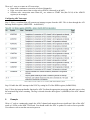
Step 4: Select the operation mode and how the ADC channel(s) should be scanned via the AD0CR register
(0x40034000).
From Table 531 in the LPC17xx User manual, NXP Semiconductors, 2010.
6
There are 3 ways to set start an A/D conversion:
Burst mode: continuous conversion of selected channel(s).
Edge: conversion starts when an edge such as EINT0 is detected (as in lab 5).
Software code: conversion starts when 0012 are written to START bits (bits 26:24) of the AD0CR
register (as in example).
Configuring ADC Interrupt:
Step 1: Select a condition that will generate an interrupt request from the ADC. This is done through the A/D
Interrupt Enable register (AD0INTEN – 0x4003400C).
From Table 533 in the LPC17xx User manual, NXP Semiconductors, 2010.
Step 2: Enable the ADC interrupt in the NVIC by setting bit 22 of the ISER0 register (0xE000E100).
Step 3: Write the interrupt handler function for ADC. Perform the appropriate processing and make sure to clear
the associated flag before returning. The flag is cleared when the data register n (AD0DRn) of the ADC channel
n is read.
5.
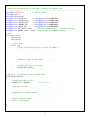
Example
Write a C code to continuously sample the AD0.5 channel and output the most significant 8 bits of the ADC
result to 8 LEDs on the MBC1700 board. You should enable the ADC to produce a result as fast as possible.
Use software code to start the conversion process.
7
Initialization Tasks:
Step 1: Enable ADC power
Step 2: Configure the ADC PCLK
Step 3: Enable pin P1.31 as AD0.5 channel
Configure the A/D control register (AD0CR)
o Set to scan pin 5 (channel AD0.5)
o Set A/D to operational mode
Processing Tasks:
Start conversion process
Continuously monitor the DONE flag, when DONE = 1, extract and output ADC result to LEDs
Repeat the process again (main while loop)
6.
References
[1].
[2].
[3].
[4].
[5].
Joseph Yiu, The Definitive Guide to ARM Cortex-M3 and Cortex-M4 Processors, Elsevier, 3rd ed, 2014.
Jonathan Valvano, Introduction to ARM Cortex-M Microcontroller, 4nd ed, 2013.
ARMv7-M Architecture Reference Manual, ARM Limited, 2010.
LPC17xx User manual, NXP Semiconductors, 2010.
Cortex-M3 Technical Reference Manual, ARM Limited, 2010.
C code:
8
/*---------------------------------------------------------------------------Lesson 16: Configure ADC to scan AD0.5 channel and output LEDs
*---------------------------------------------------------------------------*/
#include "LPC17xx.h"
// Device header
#include "LED.h"
void ADC_Init(void);
unsigned int* PCONP_ptr
= (unsigned int*) 0x400FC0C4;
unsigned int* PCLKSEL0_ptr
= (unsigned int*) 0x400FC1A8;
unsigned int* PINSEL3_ptr
= (unsigned int*) 0x4002C00C;
unsigned int* AD0DR5_ptr
= (unsigned int*) 0x40034024;
unsigned int* AD0CR_ptr
= (unsigned int*) 0x40034000;
unsigned int ADC_value = 0x0;
// use this value to pass to LED_Out function
unsigned int AD0DR5_value = 0x0;// temp storage for AD0DR5 register
//main
int main (void) {
LED_Init();
ADC_Init();
// main loop
while (1){
//Start conversion process and wait for DONE = 1
*AD0CR_ptr |= 0x01000000;
// Start = 001 --> start conversion now
AD0DR5_value = *AD0DR5_ptr;
while (!(AD0DR5_value & 0x80000000))// if not done
AD0DR5_value = *AD0DR5_ptr;
// read current value of data register
//Extract result to ADC_value
ADC_value = (AD0DR5_value >> 4) & 0x00000FFF;
//Output ADC_value to 8 LEDs
LED_Out(ADC_value);
}
}
//ADC_Init: set up ADC to scan channel AD0.5
void ADC_Init(void)
{
//Enable ADC power first
*PCONP_ptr |= 0x1000;
// bit 12 = 1
//Set PCLK for ADC
*PCLKSEL0_ptr |= 0x03000000; // bits 25:24 = 11 (12.5 MHz)
//Enable pin as AD0.5 channel
*PINSEL3_ptr |= 0xC0000000;
// bits 31:30 = 11 (p1.31)
//Select channel AD0.5
//A/D is operational
*AD0CR_ptr = 0x00200020;
// bit 5 = 1, bit 21 = 1
}
9