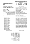
1
llllllllllllllllllllllllllllllllllllllllllllllllllll ‘
USOO5644755A
‘
Ulllt?d States Patent [19]
[11] Patent Number:
5,644,755
Wooten
[45] Date of Patent:
Jul. 1, 1997
[54] PROCESSOR WITH VIRTUAL SYSTEM
PentiumTM Processor User’s Manual vol. 3: Architecture and
MODE
Programming Manual by Intel®, 1993, (Chapters 1-4, 9-15,
20 and 22).
[75]
Inventor: David R. Wooten, Spring, Tex.
‘
Primary Examiner—Kevin J. Teska
[73] Assignee: Compaq Computer Corporation,
Assistant Examiner-Dan Filll
Houston, Tex,
Attorney, Agent or Firm-Pravel, Hewitt, Kimball 8:
Krieger
[22] Filed:
[51]
Feb‘ 24’ 1995
A processor having the prior three user addressing modes
Int. (:1.6 .................................................... .. G06F 12/10
[52] US CL
[58]
and e new virtual system mode (VSM)- “1e user modes
395/500
Field of Search . . . .
include real mode, protected mode and virtual 8086 mode.
. . . . . . . . . . . .. 395/500 800
1“ VSM’ the Pmcess‘“ can “'i?ze thc VSM addressing
395/375’ 650’ 775’ 700’ 405
References Cited
mechanism and the mode of operation prior to entering
VSM. Transitions from the user modes to virtual system
mode can be made by indirect calls through a call gate or
U-S- PATENT DOCUMENTS
5,274,791 12/1993 Bracking et a1. ..................... .. 395/405
utilize VSM memory and I/O space modes, but can also
directly “lime the m.) space and meinory °f the user In?“
5,303,378
present prior to entry mto VSM by usmg a segment override.
The uPPer 16MB of the virtual System mode memory Space
[56]
'
through vectored entries. While in VSM the processor can
4/1994 Cohen ________ __
395/700
5,355,490 10/1994 Kou ........ ..
.. 395/700
5,517,651
5/1996 Huck et al. . . . . . . .
. . . . .. 395/775
(OXITOOOOOO through 0><1T?‘?“?)iS designated as HOB-mapped
5,517,657
5/1996 Rodgers et a1. ...................... .. 395/800
virtual system mode memory. Virtual system mode logical
addresses below OxiIOOOOOO will be translated to physical
addresses by the current page table if paging is enabled
OTHER PUBLICATIONS
Reaching Physical Board Addresses in a PC From Windows
(Protected mode) Upon exitmg VSM’ any Processor T6815‘
Protected Mode David Hu?man, IEEE Man 1995_
ters that were saved are restored so the user mode operation
Intel486TM SL Microprocessor SuperSet System Design
can continue as_ if the Cm‘IIaFiOH °P§Iati°n Wm? Perfonncd
Guide, Nov., 1992 (Chapters 1-4 and 12).
Intel/1,86TM SL Microprocessor SuperSet Programmer’s Ref
erence Manual, Nov., 1992 (Chapters 1—4 and 6).
by the Kennel mtermpt servlee reutme
86 Claims, 8 Drawing Sheets
VIRTUAL SYSTEM MODE ADDRESSING
U
31
310
OFFSET
i‘ — * ~ — - - — — " _ 1
15
312/
ACCESS
RIGHTS
:
LIMIT
D
I
i
RPL
:
2
mnrx
|
I
as SEGMENT ,
:1
L
SELECTOR
f'306
U
PAGING
BASE ADDRESS
mm
______ _ _k
SEGMENT
400i
nescmmn
31
"’
0
300
PHYSICAL
ADDRESS
316/
19
314,-
4
snscron
OFFSET
l
0000
DS SEGMENT
WIOVERRIDE
7 +
U.S. Patent
Jul. 1, 1997
Sheet 1 of 8
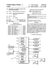
,z- 100
.x- 102
PROCESSOR
MEMORY
UNIT
U
U
5
(_
5,644,755
[104
HDSTUBUS
I
coumnuen
.
U
(_
II
r 108
no Bus
110
)
“0
RUM
,- 112
DEVICE
/ 122
EXECUTION
UNIT
/' 120
‘
ML.
\
'
1
A
BUS
INTERFACE
“DRESS
UN“
QUNTRUL
\
v + v
r 124
MEMORY
MANAGEMENT
UNIT
FIG. 1 B
US. Patent
Jul. 1, 1997
Sheet 2 of 8
5,644,755
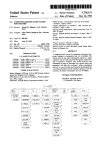
GENERAL PURPOSE REGISTERS
3
L?l fiiill
200 ACCUMULATOR
202 BASE
204 coum
HX
BX
cx
EM
EBX
Ecx
20s DATA
20s BASE POINTER
0x
EDX
EBP
210 suuRcE INDEX
212 DESTINATION INDEX
214 STACK POINTER
ESI
ED]
ESP
FIG. 2A
SEGMENT REGISTERS
1
ZZD'CUDE
222 max
224 DATA
ExTRA DATA
22s EXTRA DATA
ExTRA DATA
INSTRUCTION POINTER REGISTER
31
15
n
232
1
FIG. 2B
IP
32-BIT
EIP
U.S. Patent
Jul. 1, 1997
Sheet 3 of 8
5,644,755
EFLAGS REGISTER
31
191817161514131211109 a 7 6 5 4 3 g 1 0
v
234%
CMFDTFFFFFFFUFBFIF
AvR
NIDPUDITSZ
AH‘
12
l______‘
VSM
ALIGNMENT CHECK
EMULATOR BUSY
CONTROL REGISTER m
313029
13 16
543210‘
PCN
A
N
msnwl
w
M P
PAGING ENABLE ——-—
PRuTEcTmN ENABLE
FIG. 2D
TEMP
E'sMPE
US. Patent
Jul. 1, 1997
Sheet 4 of 8
5,644,755
VSM ENABLE REGISTER
31
878543210
23s
REsERvED
VIDSHILV
D | | E | D D s
BFEEEEEM
VSM DEBUG
LDNDRE INTERRUPT CHECK
DEFERRED INTERRUPT ENABLE
SOFTWARE EXCEPTION ENABLE
HARDWARE INTERRUPT ENABLE
ND FAULT ENABLE
LEVEL 0 ENABLE
VSM ENABLE
VSM STACK REGISTER
31
240
g 1 D
BASE
D D
VSM VECTOR BASE
a1
242
_2_ 1 D
mm ME
FIG. 2F
0 0
US. Patent
Jul. 1, 1997
Sheet 5 0f 8
5,644,755
VSM IIO PROTECTION BITMAP REGISTERS
4 3
244
VSM IIO PROTECTION BITMAP BASE ADDRESS
VSM IIO PROTECTION BITMAP
O
SIZE
\\
BITMAP
246: (K
BITMAP
—e:
if] MB
FIG. 26
I5
304 ~
REAL MODE ADDRESSING
1
OFFSET
I9
302 ~
4
SELECTOR
D
OOOO
SEGMENT
SELECTOR
FIG. 3A
U.S. Patent
Jul. 1, 1997
Sheet 6 of s
0 m.
momL
5,644,755
w.2 25
253m :2:
mom.
.GEmm
sHwza5m-2c<
qy.liE_ws|\alm5Ewesa“%m 852»%
\Nalm.
US. Patent
Jul. 1, 1997
Sheet 8 of s
3»..\.
8v\.
N8.\
5,644,755
NE .
2
o
5wé2tzu$m“a
5“Q2a%
E:25:
.UEv
5,644,755
1
2
PROCESSOR WITH VIRTUAL SYSTEM
MODE
addressing mechanisms. In this context, user memory is
memory that is used by programs when the processor is
operating in one of its operating modes. In the 386 family of
microprocessor, three different operating modes exist in
addition to SMM. Real mode is the default mode of opera
FIELD OF THE INVENTION
This invention relates to a processor and more speci?cally
tion for the microprocessor and is provided for backwards
compatibility with the earlier 8086 and 8088 processors.
to a processor having a mode of operation for emulating
standard PC hardware transparently to the operating system,
with this mode of operation allowing segment registers to
operate according to different addressing modes at the same
Protected mode was ?rst introduced in the 80286 micropro
cessor and improved in the 386 microprocesson'Protected
10
time.
BACKGROUND OF THE INVENTION
The x86 family of personal computers is well established
in the marketplace. Computer manufacturers strive to design
the highest performing systems at the lowest cost. However,
often the highest performing or lowest cost parts from which
20
segmentation unit and a paging unit. Real mode utilizes a
16-bit selector, shifted left four bits, and a 16-bit offset to
produce a 20-bit address for addressing up to 1MB of
memory. The 16-bit otfset limits the segment to a maximum
of 64k of memory. In protected mode the segment register
25
base address and the offset is increased to 32 bits, with the
segment base address and the o?iset simply being added to
provide the linear address. Protected mode may enjoy a 4GB
maximum memory segment If paging is enabled, the linear
puter is not PC compatible, the sales market for the com
desirable. Currently, PC systems designers are limited in
their ability to build systems that do not conform to PC
is rede?ned as a selector which points to a 32-bit segment
hardware standards. The reason for the limitation is that
much of the existing software that runs on PC’s makes
explicit assumptions about the nature of the hardware. If the
hardware provided by the systems designer does not con
address is then translated by the paging unit into a physical
address. Paging is a mechanism to support a large physical
address space in memory using a small amount of memory
and some hard disk space. Virtual 8086 mode addressing is
form to those standards, many software programs will not be
usable. This limits the systems designer’s ability to reduce
costs and improve functionality.
‘
Currently, the most common means of running the soft
ware on a non-compatible machine is to use a software
30
program that does complete emulation of a PC. The emu
lation is performed on each instruction. This method is
practical only for machines that are not binary compatible
with x86 PC’s because performance is poor.
One prior approach to using non-standard hardware
devices provided hardware circuitry to trap and store each
of the earlier processors. The preferred mode of operation
for the 386 processor is its protected mode. Once the
processor is in protected mode, an additional real mode
environment, called virtual 8086 mode, can be created for
backward compatibility with real mode applications.
Memory management in the processor is performed by a
a computer can be built are not PC-compatible. If a com
puter is severely diminished, thus PC-compatibility is very
mode removes most of the memory management limitations
similar to real mode in that the same l6-bit selector and
offset are used, however, it is diiferent from real mode in that
the 1MB address range can be placed anywhere within the
32-bit protected mode addressing range. Thus, three diifer
35
ent addressing schemes may exist in a computer system
using a 386 compatible processor. When the processor
switches to system management mode, a fourth hybrid
addressing mechanism is utilized. SMM generally uses a
bus access to a standard PC device and then cause the
32-bit ?at memory model addressing scheme. Segment
execution of an interrupt. The invoked interrupt handler then
determined the accessed address from the hardware
circuitry, converted this to the proper device address and
register values are stilled shifted 4 bits and added to the
oifset values, but both can be 32 bit values.
In a 386 compatible processor, addressing mechanisms
cannot be mixed between different modes of operation. For
executed that operation. This technique worked adequately
when the processor and system were relatively simple and
only for certain operating systems. However, it is not
practical on current computer systems because of increased
complexity of the processor, system and operating systems
and the frequent unavailability of an interrupt.
This interrupt problem could be solved by the use of
System Management Mode (SMM) found in certain
example, when the processor is operating in 32-bit protected
45
mode and then switches to l6-bit real mode, no protected
mode addressing selectors or offsets can be directly used. To
access a protected mode address space with a real mode
addressing mechanism, the entire protected mode addressing
mechanism including selectors, oifsets, and paging must be
calculated. Such is the case between any two addressing
processors, such as the Intel 486SL, 486 S-class and Pen 50 modes. This limitation complicates device emulation when
tium microprocessors. The SMI interrupt cannot be masked
by software and therefore is always available to the system
using SMM because the SMM code must devote signi?cant
amounts of time in an address translation process which
manufacturer. However, there are several disadvantages to
converts the address used by the user program into an
the current SMM implementations for doing hardware emu
address that SMM can use to access the same memory
lation. The ?rst is that entry to and exit from SMM requires 55 location. This process is complicated by the fact that the x86
many processor cycles. This is because SMM irnplementa
architecture supports several different addressing modes so
tions were done with the assumption that the only thing that
that the SMM code must analyze the operational mode of the
would be done in SMM is power management. This assump
user program and select an address conversion algorithm
tion caused the SMM implementor to design the processors
so that the full state of the processor was saved on entry to
SMM and the full state of the processor was restored on exit
from SMM. These operations require 100’s of processor
cycles. This entry/exit overhead of current SMM implemen
tations greatly limits it’s usefulness for emulation.
A second disadvantage is that while in SMM access to 65
user memory is limited and/or cumbersome because of the
different modes of operation and their corresponding
that is appropriate to that mode. So this addressing mode
change in SMM further exacerbates the overhead problems,
so that use of the SMI is not readily feasible.
Thus, it is desirable to have a processor that can provide
emulation transparently to the operating system and appli
cation software while using the built-in memory manage
ment features but using very few processor cycles to enter
and exit the emulation operations and not having large
address translation burdens.
5,644,755
3
4
SUMMARY OF THE INVENTION
FIG. 2D illustrates the Control Register 0 of the processor.
FIG. 2E illustrates the VSM enable register of the pro
A processor embodying the principles of the present
invention includes a processor having the prior three user
addressing modes and a new virtual system mode (VSM).
The processor is preferably compatible with Intel 486 or
higher processors, and therefore in this context, the user
modes refer to normal operational modes of the processor,
including real mode, protected mode and virtual 8086 mode.
Virtual System mode (VSM) refers to the features pro
vided by the present invention. In VSM, the processor can
utilize the VSM addressing mechanism and one other, that
cessor.
FIG. 2F illustrates the VSM stack register and VSM
Vector Base register of the processor.
FIG. 2G illustrates the VSM I/O protection bitmap reg
ister and VSM I/O protection bitmap of the processor.
FIG. 3A illustrates the real mode addressing mechanism
of the processor.
10
FIG. 3C illustrates an exemplary addressing situation for
the VSM addressing mechanism of the processor.
FIG. 4 illustrates a segment descriptor of the processor.
being the addressing mechanism of the mode of operation
prior to entering VSM.
Transitions from the user modes to virtual system mode
can be made by indirect calls through a call gate, such as by
a jump or call instruction, or through vectored entries, such
as a hardware interrupt or I/O fault. When transitioning from
the user modes to virtual system mode, the processor treats
the transition similar to a task switch, thus saving only
certain minimal processor registers depending on the VSM
entry cause. The remaining processor registers are not
disturbed, thereby providing low overhead for entry and exit
from virtual system mode.
While in the user modes, user mode addressing mecha
nisms remain unchanged. While in virtual system mode, the
processor can utilize VSM memory and I/O space modes,
but can also directly utilize the I/O space and memory of the
user mode present prior to entry into VSM. If in VSM and
a segment override is applied, the segment override register
is interpreted according to the addressing mechanism of the
25
unless otherwise indicated, the operation and features of the
30
diagram of the processor P in an exemplary computer system
35
data on the host bus 104 from the external circuits. One of
such external circuits is the memory unit 102. Memory unit
102 provides conventional memory storage for programs
and data of the computer system C. The bus controller 106
memory. Virtual system mode logical addresses in this range
are directly converted to an addressable range of the pro
is connected by an I/O bus 108 to a ROM 110 and several
45
I/O devices 112, such as a keyboard, ?oppy disk, hard disk,
serial port, parallel port, and monitor. The items referred to
herein but not explicitly shown on the ?gures are otfered for
illustrative purposes and are not generally important to the
enablement of the present invention since the PC architec
ture is well known to those of ordinary skill in the art.
out modi?cation (real mode).
VSM may be exited by one of three instructions. Upon
exiting, any processor registers that were saved are restored
operation were performed by its own interrupt service
C. The processor P is connected to a memory unit 102 and
a bus controller 106 by a host bus 104. Processor P provides
the data, address and control signals to the host bus 104 for
communicating with external circuits, and likewise receives
virtual system mode memory space (OXffOOOOOO through
0><?’tfff?’) is designated as non-mapped virtual system mode
so the user mode operation can continue as if the emulation
of the 486 and Pentium are assumed in this description. For
any details, reference should be made to the appropriate data
book.
The processor of the present invention is designed to be
used in a IBM compatible computer. FIG. 1A is a block
executes in a 32-bit logical space. The default data size is
32-bits, but overrides may be used. The upper 16MB of the
cessor. Virtual system mode logical addresses below
0><ff000000 will be translated to physical addresses by the
current page table if paging is enabled (protected mode).
Otherwise, these addresses become physical addresses with
DETAILED DESCRIPTION OF THE
PREFERRED EMBODIMENT
The processor of the present invention is preferably based
on an Intel compatible 486 or Pentium class microprocessor,
however the invention could also be used with an Intel 386
class microprocessor. The use of the features described
herein could also be used with other types of microproces
sors. For purposes here, the terms microprocessor and
processor can be used interchangeably. The new mode
de?ned according to the present invention is in addition to
the existing modes of the 486 and Pentium processors, and
processors remain unchanged. Familiarity with the operation
mode of operation prior to entering VSM.
While in virtual system mode, memory addresses may be
paged or non-paged depending on the user mode from which
virtual system mode was called. Virtual system mode code
FIG. 3B illustrates the protected mode addressing mecha
nism of the processor.
50
routine.
Additionally, the processor of the present invention could be
used in a wide variety of computer systems.
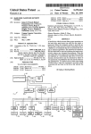
FIG. 1B illustrates the major portions of processor P. The
BRIEF DESCRIPTION OF THE DRAWINGS
processor P has a bus interface unit 120 connected to an
preferred embodiment is considered in conjunction with the
122 contains logic necessary for executing instructions,
including an instruction prefetch and predecode unit, a
control unit for decoding and sequencing of instructions, and
an arithmetic logic unit containing a set of registers for
executing each individual instruction. The execution unit
122 works in conjunction and is connected to the memory
management unit 124. The memory management unit 124
contains the logic necessary for address generation and
protection checking and includes a segmentation unit and a
execution unit 122 and a memory management unit 124. Bus
A better understanding of the present invention can be 55 interface unit 120 provides data, address and control signals
for communicating with external circuits. Execution unit
obtained when the following detailed description of the
following drawings, in which:
FIG. 1A is a block diagram illustrating a computer system
C containing a processor according to the present invention.
FIG. 1B is a block diagram of the processor.
FIG. 2A illustrates the general purpose registers of the
processor.
FIG. 2B illustrates the segment registers and instruction
pointer register of the processor.
FIG. 2C illustrates the ?ags register of the processor.
65
paging unit. These functions will be described in more detail
below.
5,644,755
5
6
The bus controller 106 translates the processor P cycles
Turning now to FIG. 2B, six 16-bit segment registers and
the instruction pointer are shown. The six 16-bit segment
registers are used for segmentation, discussed below, and are
named the code segment register (CS) 220, the stack seg
into 110 bus 108 cycles for providing communication
between the processor P and the I/O devices 112. In the
preferred embodiment of the computer system C, the I/O
devices 112 may not be PC-compatible. Compatibility is
important because in the PC, software generally expects
ment register (SS) 222, the data segment register (DS) and
the extra data segment registers (ES, FS and GS) 226. The
certain registers and bits to be present in most I/O devices.
If a device is designed into a computer that is not
compatible, the software would not be able to communicate
directly with the device, therefore the computer would not
operate properly. A processor embodying the present inven
tion would handle non-compatible device by having a facil
ity for: interrupting the processor when software tries to
commonly used names are the CS, SS, DS, ES, FS and GS
segment registers. The l6-bit segment registers hold values,
called selectors, identifying the currently addressable
10
memory segment. A segment is simply a section of memory
whose boundaries can be described by a base address and an
offset from the base address. The selector in CS indicates the
current code segment, the selector in SS indicates the current
stack segment while the selectors in D8, ES, FS and GS
indicate the current data segments.
The instruction pointer 232 holds the o?’set of the next
access the known non-PC-compatible device; and process
ing the operation transparently to the software so that the
software believes the device is PC compatible. The feature
that provides these bene?ts is hereinafter known as virtual
instruction to be executed. The 32-bit instruction pointer 232 .
system mode (VSM).
The processor P has four modes of operation, namely, real
mode, protected mode, virtual 8086 mode and virtual system
mode. In this context, real mode, protected mode and virtual
20
8086 mode are referred to as user modes. Those having
ordinary skill in the art will recognize that the user modes
refer to the modes of operation for executing conventional
software such as the operating system and applications
software. A complete description of real mode, protected
25
mode and virtual 8086 mode can be found in the Intel 486
microprocessor databook. Brie?y, the purpose of real mode
operation is for backward compatibility with the earlier
16-bit, 8086 processor. Additionally, real mode is the default
mode of the processor and is required to setup the processor
for protected mode operation. Real mode and virtual 8086
mode are limited to accessing only lMByte of physical
memory and are thus not the preferred mode of operation.
30
is commonly referred to as the EIP register and the 16-bit
instruction pointer 232 is named the IP register. The oifset
contained in the instruction pointer 232 is always relative to
the base of the code segment, thus the logical address for the
next instruction address is calculated by adding the o?’set to
the code segment base address.
Referring now to FIG. 2C, the ?ags register 234 of the
processor P is shown. The ?ags register 234 contains a 32-bit
value named EFLAGS, while the lower 16-bits of ?ags
register 234 contain the l6-bit value named FLAGS. The
16-bit portion is used when executing 8086 and 80286 code.
Bit 17 is de?ned as the virtual 8086 mode (VM) ?ag and is
set by the processor P if virtual 8086 mode is the current
operating mode. Bit 3 is de?ned as the emulator busy (EB)
?ag and is set when, in virtual system mode, an exception is
taken causing VSM to again be entered, and is cleared when
Protected mode provides access to the memory management
capabilities of paging and protection, discussed below, and
the exception routine is exited. When set, and the next
operates in a 32-bit environment with 4GByte physical
memory limit and therefore, in conjunction with virtual
system mode, is the preferred mode of operation of the
instruction executed causes an exception that enters VSM,
the pushed EPLAGS/FLAGS image will have the EB ?ag
processor. Within protected mode, software can perform a
performed transparently to the conventional software
executing on the computer system. Abetter understanding of
then a deferred interrupt fault is generated. Bit 31 is de?ned
as the Virtual System Mode (VSM) ?ag and is set when
virtual system mode is entered and cleared when virtual
system mode is exited by an IREI‘ instruction or the ?ags
register 234 is loaded without the VSM ?ag set. The VSM
?ag cannot be set with a Pop Stack into Flags (POPF)
instruction or an Interrupt Return (IRET) instruction. It may
be set by a task switch if VSM is enabled. All de?ned ?ags
VSM can be obtained from the following detailed descrip
tion.
and VSM ?ag, are used by the user modes. When in virtual
sets. If the instruction does not cause a fault or exception,
task switch to enter into tasks known as virtual 8086 mode
tasks thus emulating real mode as a task from within the
protected mode of operation.
Virtual system mode (VSM) provides an additional mode
of operation from which a VSM emulation task can be
of the ?ags register 234, with the exception of the EB ?ag
REGISTERS
The processor P contains eight general purpose registers
50
which are used for both address calculation and data opera
tions and can support data operands of 1, 8, 16 and 32 bits.
FIG. 2A illustrates the general purpose registers of the
processor P. The eight registers are: the accumulator register
(AX) 200, the base register (BX) 202, the count register
(CX) 204, the data register (DX) 206, the base pointer
register (BP) 208, the source index register (SI) 210, the
destination index register (DI) 212, and the stack pointer
register (SP) 214. Those having ordinary skill in the art will
recognize the terms in parenthesis as the commonly used
names for the 16-bit form of the registers. The 32-bit form
of the general purpose registers are named EAX, EBX,
ECX, EDX, ESI, EDI, EBP and ESP respectively. The least
signi?cant l6-bits of the 32-bit general purpose registers can
be accessed separately by using the l6-bit names of the
registers AX, BX, CX, DX, SI, DI, BP and SP as described
above.
system mode, instructions are additionally responsive to the
EB ?ag and VSM ?ag so that if VSM code is running and
an additional exception is again taken to VSM code, upon
return from the subsequent exception, processing will return
to the original VSM routine instead of exiting VSM code
completely.
Referring now to FIG. 2D, Control Register 0 (CR0) 236
55
of the processor P is shown. CRO contains 6 bits for control
and status purposes including the Paging Enable (PG) bit
and the Protection Enable (PE) bit. Those skilled in the art
will recognize that these bits help de?ne the user modes of
operation in the processor P, and are accessed by load and
store instructions. If the PG bit and the PE bit are cleared, the
processor P is operating in real mode. If the PG bit is cleared
and the PE bit is set, the processor P is operating in protected
mode. If the PG bit and the PE bit are set, the processor P
is operating in paged protected mode. When the PG bit is set
65
and the PE bit is cleared, the processor state is unde?ned and
loading this combination will cause an exception. However,
if this is attempted while operating in virtual system mode,
5,644,755
7
8
loading this combination will not raise an exception but will
enable paging, thus having the effect of enabling paging for
TABLE l-continued
a real mode application. If the PE-bit is set and the VM-bit
is set, the processor is operating in virtual 8086 mode.
Virtual system mode selection is controlled by a bit in the
Bits
Name
Description
VSM Enable register 238, discussed below, and is indepen
protection bitmap is checked last
(after memory addresses have been
dent of the user mode and therefore does not atfect the use
of the PG, PE or VM bits.
redundant.
validated).
If SE is set, this bit becomes
Referring now to FIGS. 2E-G, four VSM registers are
shown. FIG. 2E illustrates the VSM enable register 238 for
enabling most VSM functions. FIG. 2F illustrates the VSM
Hardware Interrupt Enable. Setting
this bit to ‘1’ causes all external
hardware interrupt events (INTR and
NMI) to be dispatched through the
Hardware Interrupt Vector.
Software Exception Enable. Setting
stack register 240. FIG. 26 illustrates the VSM vector base
register 242. FIG. 2G illustrates the VSM I/O protection
this bit to 1 causes all exception
bitmap register 244 and it’s corresponding bitmap 246. The
conditions generated by user mode
four VSM registers are used only during execution in virtual
software to be dispatched through the
Software Interrupt Vector. When this
bit is set, 110 protection faults
generated from the I/O protection
bitmap in the TSS will fault using the
system mode and are not used by user mode tasks. These
registers are accessible from any user mode until VSM is
enabled. 'lhrning now to FIG. 2B and Table 1 below, the
format of the VSM Enable register 238 is de?ned.
VSM semantics and through the VSM I/O
protection fault vector. Also, the
I/O protection bitmap in the TSS will
20
TABLE 1
be checked instead of the VSM I/O
Bits
Name
Description
protection bitmap (after address
0
VSME
VSM Enable. Setting this bit enables
Virtual System Mode. This bit may
only be set when the processor is
executing in real mode or protected
Deferred Interrupt Enable. When this
checking).
25
bit is set, a VSM Deferred Interrupt
is generated when the 1P bit is set by
usercode.'l‘hisbitisusedin
combination with the Ignore l'F bit to
allow VSM to manage hardware
mode level 0. Once set, accesses to
this or any other VSM register may
only be made while the processor is
interrupts regardless of the IF
manipulations by other software. If a
executing in VSM.
Level 0 Enable. When this bit is set,
all calls that target level 0 will
hardware event occurs that needs to be
cause a switch to VSM. When the RPL
have 1F cleared, indicating that it is
of the selector in the call gate is 0,
VSM will be entered using the o?’set
portion of the gate as the starting
address in VSM logical space. If the
gate speci?es an argument value, the
speci?ed number of words are copied
not capable of accepting a hardware
interrupt at this time. If this
occurs, the VSM hardware interrupt
handled by non-VSM code, that code may
35
handler should set DIE so that VSM
will regain control when the user code
sets lF. The deferred interrupt may
then be delivered.
to the VSM stack. This bit should
only be set when the OS is VSM aware.
Ignore Interrupt Flag. Setting this
'I‘hecall?'ameontheVSMstackis
sligh?y different from the call frame
for,a level 0 call.
bit causes the processor to allow
entry to VSM when any external
hardware interrupt pin is active
regardless of the setting of lF in
Setting this bit also causes the
processor to maintain the VSM stack in
the TSS of a task. When LOE is set,
EFLAGS. IF is not ignored in VSM.
7
VDB
VSM mode debug. Setting this bit
enables the processor dependent debug
exceptions when running in VSM
The level 0 'ISS is not used. A task
switch to a TSS with the VSM bit set
in the saved EFLAGS image will cause
8-31
Reserved
Reserved for future use.
thenewtasktobestartedinVSM.l.f
FIG. 2F illustrates the VSM stack register 240 and VSM
vector base register 242. The VSM stack register 240 is a
the level 0 stack pointer in the TSS
’ contains the base of the VSM stack.
2
ICE
LOE is not set, the VSM bit in the
ETLAGS register is ignored on a task
switch.
110 Fault Enable. Setting this bit to
50
of the VSM stack. The VSM vector base register 242 is also
a 32-bit register indicating the logical base address of the
VSM interrupt vector table. These registers are both acces
1 causes all I/O accesses by other
than VSM code to be checked against
the VSM I/O protection bitmap. If the
I/O location is ‘protected,’ then
sible from any user mode until VSM is enabled. In both
55
accesses will cause a fault to VSM
through the VSM IIO protection fault
processor is running in protected
mode, the protected mode 110
protection bit map will be checked
exceptions generated before the VSM
IIO protection bitmap is checked.
bitmap 246 are illustrated. The 28-bit base address ?eld
de?nes the physical base address of a physically contiguous,
16-byte-aligned, VSM I/O protection bitmap 246. The size
VSM IIO faults are generated after all
other access checks have been
address checks. The VSM I/O
registers, bits 0-1 are always “0” and writing a “1” is
ignored and will not produce an exception.
Turning now to FIG. 2G, the VSM I/O protection bitmap
register 244 and its corresponding VSM I/O protection
vector. When this bit is set and the
completed. The normal protected mode
I/O protection bitmap is checked and
exceptions generated before any
32-bit register indicating the starting logical address, or top,
?eld is a 4-bit value that when raised to the power of two
indicates the size, in bytes, of the bitmap. For example, a
value of 0 indicates a single byte table, a value of 1 indicates
65
a 2-byte table and a value of 12 indicates an S-Kbyte table
(64 kbits). Each bit of the bitmap speci?es whether the
byte-wide address associated with the bit can be accessed by
5,644,755
10
a user mode operation. This bitmap is in addition to the I/O
defaults can be overridden. Special segment override pre
?xes allow a speci?c segment register to be used in place of
permission bitmap of the Intel 486 microprocessor. Thus, the
normal I/O permission bitmap is checked, and exceptions
generated before the VSM I/O protection bitmap is checked.
the default segment registers. However, since the addressing
mechanism for real mode and protected mode are
incompatible, real mode selectors and o?sets cannot be used
When the VSME-bit is set, every 110 access is con?rmed
through the VSM I/O protection bitmap register. If access to
when operating the processor P in protected mode, and
similarly, protected mode selectors and offsets cannot be
used when operating the processor P in real mode.
that address is protected, then the user mode operation is
vectored into a VSM handler.
MEMORY MANAGEMENT
10
A similar problem is found in those processors having a
system management mode. The addressing mechanism of
Memory management in the processor P is performed by
the processor in system management mode, is incompatible
a segmentation unit and a paging unit. Segmentation is a
with either real mode or protected mode, thus if using a
processor with system management mode and emulation is
desired, the user mode addresses must be translated into
mechanism for providing many independent address spaces.
Paging is a mechanism to support a large physical address
space in memory using a small amount of memory and some 15 addresses compatible with the SMM addressing mechanism.
hard disk space. Addresses are generated diiferently depend
ing upon the mode of operation.
This procedure is costly in terms of processing time.
When the processor Pis operating in virtual system mode,
the prior mode of the processor P (the mode of operation
when the VSM event occurred), can be determined by the
The processor has three distinct address spaces known as
logical, linear, and physical. An address issued by a program
is a logical address and consists of a selector and an offset.
state of the PE-bit and the VM-bit VSM can therefore be
Generally, the selector identi?es a particular segment, and
looked at as a submode of each of the user modes. When a
the offset identi?es an address within the segment. Selector
segment register override is requested in VSM, the segment
values are used by loading the value into the corresponding
selector value is interpreted as being either a segment base
address (real mode or virtual 8086 mode) or an index
segment register discussed above. By using segments and
o?’sets the processor can access a total of 64 Terabytes of 25 (protected mode) according to the context of the processor
logical address space in protected mode. The segmentation
P as de?ned by the PE-bit and VM-bit. Thus, when in virtual
unit translates the logical address into an address for a
system mode, the addressing mechanism of the previous
continuous, unsegrnented address space, called the linear
address space. If the paging unit is enabled, the linear
address is translated into the physical address, otherwise, the
linear address corresponds to the physical address. The
mode of operation can be used for VSM operations, there
processor can access up to 4 Gigabytes of physical address
space.
particular segment selector 302 loaded in a segment register '
(220—226). The segment descriptor 400 consists of a seg
ment base address 402, a segment limit 404, and segment
attribute and access right bits 406. The segment descriptor
400 contains two access bits, called DPL or descriptor
As stated, a logical address consists of a selector and an
oifset. One of the primary differences between real mode
and protected mode is the way the segmentation unit trans
lates the logical address into a linear address.
FIG. 3A illustrates the real mode addressing mechanism.
In real mode, the segmentation unit shifts the 16-bit selector
302 left four bits and adds it to the 16-bit offset 304 to create
a physical address 300. No paging is used and all tasks
operate at the most privileged level. Virtual system mode
addressing is similar, except that no segment values are used
and the offset is 32-bit based, not 16-bit based as shown.
Because no segment values are used, all offsets are zero
fore making emulation much simpler.
Returning to FIG. 4, the segment descriptor register
contains the segment descriptor 400 corresponding to the
35
privilege level bits, which de?ne the least privileged level at
which a task may access that descriptor, and an attribute bit
termed the D-bit which indicates the default length for
operands and o?’sets. If D=l then 32-bit operands and 32-bit
addressing modes are assumed. If D=O then 16-bit operands
and addressing modes are assumed. Regardless of the
default precision of the operands or addresses, the processor
45
based. Therefore VSM addressing is a ?at 32 bit model.
FIG. 3B illustrates the protected mode addressing mecha
nism. Also referring brie?y to FIG. 4, in protected mode, the
16-bit selector 302 is used to specify an index to a segment
50
602 which the segmentation unit then adds to a 32-bit o?’set
304 to create the linear address 308. Each selector has a
In real mode, protected mode and virtual 8086 mode,
of IMB or 4 GB. The AVL, P, S, andA bits are used as in
Virtual System Mode Addressing
corresponding segment descriptor 400 which is automati
in more detail below.
specifying an override pre?x. The segment base address 402
de?nes the starting address of the segment. The segment
limit 404 is combined with the granularity (G) bit to de?ne
a logical page size of 1 byte or 4kbytes with an otfset limit
the 486 or Pentium and are described below.
descriptor 400 containing the 32-bit segment base address
cally loaded into a segment descriptor register when a
selector value is loaded into a segment register. The two
lower bits of the 16-bit selector 302, are termed the requestor
privilege level bits (RPL) and de?ne the privilege level of
the original supplier of the selector. Privileges are discussed
is able to execute either 16-bit or 32-bit instructions by
55
In virtual system mode, addresses are generated assuming
32-bit addressing without segmentation, and the ?at memory
model is employed, thus resulting in code, stack and data
segments pointing to the same 4 GB address space. If a
segment override is applied, then the address generation is
performed using the speci?ed segment register(s) with the
contents of the segment register(s) interpreted as being
either a segment value (real mode or virtual 8086 mode) or
there are two main types of non-system segments: code and
a selector (protected mode) according to the context of the
data. Instructions do not explicitly need to specify which
processor prior to entering VSM as de?ned by the PE-bit and
segment register is used to access a segment. In general,
VM-bit, followed by paging checks if enabled, as similarly
code references use the selector in the CS register, data 65 performed in user mode addressing. For example, if the
references use the selector in the DS register, and stack
processor was in real‘ mode, PE=0 and VM=0, prior to
references use the selector in the SS register, however, the
entering VSM (i.e., a VSM event occurred while in real
5,644,755
11
12
mode) and then if while in VSM a segment override is
Therefore, if a segment override pre?x is present and, if the
applied, the VSM addressing mechanism will interpret the
address using the real mode addressing mechanism.
FIG. 3C illustrates the exemplary addressing situation
D-bit is 0 and no address pre?x is present or if the D-bit is
1 and an address pre?x is present then CX is used, otherwise
ECX is used. The foregoing discussion of LOOP/REP
Counter usage is surmnarized in Table 3.
described above. The default mode, of an instruction is
always 32-bits. Thus, the segment selector 312, here illus
TABLE 3
trated by the code segment, indexes to a base address 402
that is the combined with an o?set 310 to produce the linear
address 308. Normally the paging unit 306 is disabled in
VSM and the linear address is also the physical address. In
the ?at memory model used by VSM the base address 402
10
is set to OXOOOOOOOOh and the offset produces the 32-bit
address. If a segment ovenide is applied, here represented as
a data segment, the segment selector is interpreted according
to the context of the processor prior to entering VSM-—in
this case real mode. Therefore the DS selector 314 is shifted
left four bits and added to an offset 316 to produce a 20-bit
real mode address. Protected mode addresses can be sirni
Segment
Override
Pre?x
Address
Size
Pre?x
D-bit
Count
Register
Used
No
No
Yes
Yes
Yes
Yes
No
Yes
No
No
Yes
Yes
X
X
0
l
0
1
ECX
CX
CX
ECX
ECX
CK
The processor P can support 8-bit, 16-bit and 32-bit data
types. While in virtual system mode, the default data size is
32-bits, regardless of the D-bit, unless an instruction explic
itly calls for a byte operand. Additionally, a operand-size
larly generated but only if the processor P was in protected
mode prior to entering VSM.
When a segment override pre?x is present on an
instruction, the address modulus of the operand is deter
mined by the D-bitin the code segment descriptor. The D-bit
in the code segment descriptor register represents the default
pre?x may be used to force a 16-bit operand. If a segment
override pre?x is present, the size of operands that are not
explicitly byte operands are controlled by the D-bit in the
addressing and data size for the user mode. For instructions 25 code segment descriptor and an operand-size pre?x. The
which have two memory operands, the D bit only affects the
foregoing discussion of VSM operand sizing is summarized
address modulus of the operand associated with the segment
in Table 4.
override pre?x. For example, if the D-bit is O and a move
data from string to string instruction (MOVS) is executed,
the source address will be ESI (a VSM memory source) and
the destination address will be EDI (a VSM memory
destination). If the same instruction is executed except a DS
user mode segment override is applied, the source address
will be DSzSI (a user mode source) and the destination will
be EDI (a VSM memory destination). An instruction that
TABLE 4
30
35
uses ES as the default segment (i.e., no segment override
allowed) may only have an address size pre?x. An instruc
tion that defaults to the DS segment and allows a segment
override pre?x, may use any segment as the override.
Segment
Operand
Override
Pre?x
Size
Pre?x
D-bit
Data
Size
No
No
Yes
Yes
Yes
Yes
No
Yes
No
No
Yes
Yes
X
X
0
l
0
1
32
16
16
32
32
16
Instructions that have two memory operands (e.g., MOVS,
CMPS)may have two segment pre?xes. For these
instructions, if the ES override pre?x is present, it will apply
to the destination address only. Any segment ovenides other
that has two memory operands, the size is determined by the
combination of the D-bit in the code segment descriptor and
than ES will apply to the source operand. ES may not be
the operand-size pre?x and will apply to both operands. The
used twice to force its use for both source and destination.
combinations for an instruction having two memory oper
ands and not explicitly a byte operand are listed in Table 5.
Any segment register other than ES can be used as a segment
override pre?x to modify the source address. The destination
operand address alone can be modi?ed by using an ES
The foregoing discussion of VSM segment override pre?xes
is surmnarized in Table 2.
TABLE 2
Segment
Address
Override
Pre?x
Size
Pre?x
D-bit
Address
Modulus
No
Yes
Yes
Yes
Yes
X
No
No
Yes
Yes
X
0
1
0
1
32
16
32
32
16
In virtual system mode, instructions such as Loop Control
with CX Counter (LOOP) and Repeat Following String
Operation (REP) which have an implied CXIECX counter
will use ECX unless an segment override and/or address
pre?x is present. If only an address pre?x is present, then CX
is used as the count register. If a segment override pre?x is
present, then the D-bit of the code segment descriptor will
govern the choice along with an address pre?x, if present.
If a segment override pre?x is present on an instruction
TABLE 5
55 Segment
Override
Pre?x
0perand
Ad
dress
Size
Pre?x
Size
Pre?x
Data
D-bit Size
Source
Dest’n
Count
None
None
None
None
DS
DS
DS
DS
DS
65 DS
DS
No
No
Yes
Yes
No
No
No
No
Yes
Yes‘
Yes
No
Yes
No
Yes
No
No
Yes
Yes
No
No
Yes
X
X
X
X
0
1
0
1
0
1
0
ESI
ESI
ESI
ESI
SI
ESI
ESI
SI
SI
ESI
ESI
EDI
EDI
EDI
EDI
EDI
EDI
EDI
EDI
EDI
EDI
EDI
ECX
CX
ECX
CX
CX
ECX
ECX
CX
CX
ECX
ECX
32
32
16
16
16
32
l6
32
32
16
32
5,644,755
13
14
TABLE 5-continued
common. The accessed (A) bit is set whenever the processor
accesses a descriptor. The executable (E) bit indicates if a
segment is a code (E1) or data segment (E=0).
Segment
Operand
Ad
dress
Override
Pre?x
Size
Pre?x
Size
Pre?x
Data
D-bit Size
Source
Dest’n
Count
DS
Yes
Yes
1
16
SI
EDI
CX
DS, ES
DS, ES
DS, ES
DS, ES
DS, ES
DS, ES
DS, ES
DS, ES
No
No
No
No
Yes
Yes
Yes
Yes
No
No
Yes
Yes
N0
No
Yes
Yes
0
1
0
1
0
1
0
1
16
32
16
32
32
16
32
16
SI
ESI
E81
SI
SI
E81
ESI
SI
DI
EDI
EDI
DI
DI
EDI
EDI
DI
CX
ECX
ECX
CX
CX
ECX
ECX
CX
In a data segment descriptor, the expansion direction (ED)
bit speci?es if a segment expands downward (ED=1, i.e.,
stack) or upward (ED=O, i.e., data). Data segments are
readable and the write (W) bit controls the ability to write
into a segment. Data segments are read-only if W=0.
10
15
While in virtual system mode, memory addressing to
VSM memory may be paged or non-paged and is dependent
on whether paging is enabled by ?1e user mode operations.
VSM code executes in a 32-bit logical space and VSM
addresses are generated as 32-bit addresses by default. The
A code segment may be designated execute-only or
execute/read as determined by the read (R) bit. Code seg
ments are execute only if R,=0, and execute/read if R=1.
Code segments may never be written to, however in virtual
system mode, the DS segment register may be loaded with
a code selector with no exception generated. Upon loading
the DS register, the access rights for the segment will be
forced to 13:1 (code), ED=1 (expand down segment) and
W=l (read/write).
Protection checking is also automatically performed when
20
a task switch is undertaken. Call gates are used to change
privilege levels and are used to control access to entry points
within the target code segment. Call gates are primarily used
upper l6-MByte of VSM memory (OX?’OOOOOO through
OX?’?ii’?) is designated as non-mapped VSM memory. Logi
to transfer program control to a more privileged level. The
cal addresses generated in this range are converted to an
a selector and an o?‘set which point to the start of a routine,
and an argument count which speci?es how many param
eters are to be copied from the caller’s stack to the stack of
the called routine. The argument count ?eld is only used on
call gates when there is a change in the privilege level.
If the level 0 enable (LOE) is set in the VSM enable
call gate descriptor consists of three ?elds: the access byte,
address that is in the upper l6-Mbyte of the physically
addressable range of the processor P. VSM logical addresses
generated below OXEOOOOOO are translated to physical
addresses by the current page table if paging is enabled,
otherwise these addresses become physical addresses with
out modi?cation.
30
If a segment override is applied when addressing VSM
memory, and the resulting logical address references
memory at or above OX?’OOOOOO, the address is deemed not
to reference non-mapped VSM memory and is translated
into a physical address by the paging unit, if enabled. If no
segment override pre?x is used, the access is to VSM
memory.
list is present, the speci?ed number of words are transferred
from the stack of the calling program into the VSM stack.
When VSM is entered due to a level 0 call, the entry point
for the routine cannot be the same as it is for VSM code
calling the same routine. A VSM routine that is callable from
privilege levels 1, 2 and 3 requires a stub routine. This stub
routine may simply call the VSM routine, but when a return
is made to the stub routine, it is responsible for adjusting the
stack pointer (ESP) pushed on the stack so that the user stack
will not pop the call values. The stub routine then executes
PRUI‘ECI'ION
The processor P has four levels of protection for support
ing multi-tasking operating systems and to isolate and
protect user programs from each other and the operating
system. The privilege levels control the use of privileged
instructions, I/O instructions, and access to segments and
segment descriptors. Level 0 is the most privileged and level
3 is the least privileged. The current privilege level (CPL)
speci?es the task’s privilege level which equals the privilege
register 238, indirect calls through a call gate will enter
virtual system mode if the requestor privilege level (RPL) of
the gate’s selector is 0. In this case the calling routine pushes
ESP, EFLAGS and HP onto the stack, and the gate’s otfset
value is placed in EIP. If the gate indicates that an argument
45
an IREI' that returns control to the outer level. If EFLAGS
is used to convey the return conditions, the stub routine must
also update the pushed EFLAGS values before returning.
level of the code segment being executed. For virtual system
mode addressing, CPL is level 0. While in VSM, for
purposes of protection checking of user mode addresses,
I/O SPACE
The processor has two distinct physical address spaces,
namely, memory and I/O space. The 1/0 space consists of 64
kbytes of physical address space. The processor includes a
CPL is determined by the settings of the PE-bit, the VM-bit
and the two low bits of the CS register. If PE=0, then CPL
VSM I/O protection bitmap register 244, as shown in FIG.
is assumed to be level 0. If PE=1 and VM=1, then CPL is
2G. The VSM I/O protection bitmap register 244 contains a
assumed to be level 3. If PE=1 and VM=0, then the CPL is
size ?eld and an address ?eld, as discussed above. While in
the low two bits of the CS segment register.
55 virtual system mode and the hardware interrupt enable bit is
Segmentation provides another basis for protection. All of
set, the processor consults the VSM I/O protection bitmap
the descriptors in a system are contained in tables recog
246 to determine if access to the I/O port is allowed, or a
nized by processor hardware. As described above, segment
descriptors are 8-byte quantities which contain the attribute
VSM interrupt to be generated instead Ifthe bit correspond
information about a given segment. These attributes include
the access rights such as: protection level, read, write or
execute privileges, the default size of the operands, and the
type of segment. There are two main types of non-system
fault vector for emulation. The VSM I/O protection bitmap
address register 244 is only accessible in virtual system
segments: code segments and data segments (includes
stacks). The segment (S) bit determines if a given segment
is a system segment (8:0), or a code or data segment (S=1).
Code and data segments have several descriptor ?elds in
ing to an I/O address is set, then an access to that address will
cause VSM to be entered through the VSM I/O protection
mode.
65
INTERRUPTS/EXCEP'I'IONS
Interrupts and exceptions alter the normal program ?ow in
order to report errors or handle external events or excep
5,644,755
15
16
tional conditions. All VSM events except a VSM Stack Fault
are enabled in the VSM Enable register 238. If the VSM
vector 3. If the VSM hardware interrupt handler determines
that the interrupt needs to be handled by non-VSM handlers,
the deferred interrupt enable (DIE) bit should be set so that
the VSM deferred interrupt handler will regain control when
the user code sets the IF-bit again and the deferred interrupt
event is not enabled, then interrupt processing occurs
through the conventional interrupt descriptor table. If the
VSM event is enabled, for VSM events, interrupts and
exceptions are handled through a VSM vector table. This
vector table contains a single 32-bit value for each VSM
event that points to the entry point for the VSM handler as
de?ned in Table 6. The VSM vector table is located in VSM
can then be delivered to the user code.
If the DIE-bit is cleared in the VSM enable register 238
but the emulator busy (EB) bit is set in EFLAGS and the user
mode program executes an instruction that sets the IF-bit,
but does not cause any other fault or trap, then a fault is taken
memory starting at the logical address contained in the VSM
vector base register 242.
through VSM vector 1. If the DIE-bit is set in the VSM
enable register 238 and the emulator busy (EB) bit is set in
TABLE 6
Vector
O?‘set
VSM Event
0
1
00h
04h
VMI Instruction Trap
Deferred Interrupt 'I‘rap/Fault
2
08h
VSM I/O Protection Fault
3
4
OCh
10h
Hardware Interrupt
VSM Software Exception
5
6
7
14h
18h
lCh
VSM Stack Fault
RESERVED
RESERVED
EFLAGS and the user mode program executes an instruction
that sets the lF-bit, then a fault is taken through VSM vector
1, but the IF-bit is left cleared.
If the I/O fault enable (IOE) bit in the VSM enable register
238 is set and an I/O access is made to a location that has the
20
VSM interrupts and exceptions are referred to here as
VSM events. When an VSM event occurs, the following
instruction causing the I/O access references more than one
byte, any individual byte that has a corresponding bit in the
VSM I/O protection bitmap 246 set will generate a U0 fault
through this vector. When this fault is taken, the VSM stack
actions happen. First, at a minimum, the current program
address (EIP) and the ?ags register 100 (EFLAGS) are
pushed on the stack to allow resumption of the interrupted
will contain the following pushed register values, starting
program. If the processor is not in virtual system mode when
the VSM event is generated, the current stack pointer (ESP)
is pushed ?rst before the current program address and ?ags
register 100. Thus, the VSM-bit in the pushed EFLAGS
value will indicate whether the stack pointer (ESP) was
corresponding bit in the VSM I/O protection bitmap set to 1,
then that I/O device requires a VSM handler, and the
processor will enter virtual system mode and begin execut
ing at the location pointed to by VSM vector 2. If the
with the ?rst pushed: ESP, EFLAGS, EIP, EAX, Next
30
Instruction EIP, SEG REG and VFLAGS. Table 7 de?nes the
stack values.
TABLE 7
pushed on entry so that it can be restored on VSM exit. Next,
an 8-bit vector is supplied to the processor which identi?es
Stack
Offset
the conventional entry in the user interrupt table. Interrupts
have externally supplied vectors, while exceptions have
internally supplied vectors. The processor then determines
from the user vector which of the eight VSM vectors is
applicable. The VSM vector table contains the starting
address of the VSM interrupt service routine. Then the VSM
interrupt service routine is executed. VSM code can then
determine the source of the interrupt and respond
appropriately, thus handling conventional interrupts conven
tionally or handling non-conventional interrupts with VSM
ESP (always)
EFLAGS
EIP
EAX
Next
Instruction
Ell>
SEG REG
VFLAGS
45
EAX contains the I/O address referenced by the instruc
tion causing the fault. Next Instruction EIP contains the
below.
If enabled in the VSM enable register 238, a Virtual
logical address of the instruction following the faulting
System Mode Interrupt (VMI) instruction will be trapped
50
instruction of the interrupted routine. If the VSM emulation
is completed allowing execution to resume after the faulting
instruction, the VSM handler will then move this value to the
are exceptions that are reported immediately after the execu
tion of the instruction which caused the problem. Faults are
exceptions that are detected and serviced before the execu
location of the saved EIP, thus effectively changing the fault
into a trap. The SEG REG contains a copy of the segment
register pre?x speci?ed in an OUTS instruction. Its contents
tion of the faulting instruction.
If the Deferred Interrupt Fault/Trap (DIE) bit is set in the
are only de?ned for an OUTS instruction that has a segment
pre?x other than the DS segment. The pushed VFLAGS
VSM Enable register 238, and a user mode program
executes an instruction that sets the interrupt enable (IF-bit)
in EFLAGS, a trap is taken through VSM vector 1. A
deferred interrupt fault/trap is required when the following
18h
14h
10h
OCh
08h
04h
00h
emulation code. The VSM vectors are individually described
and the exception handled by VSM vector 0, thus immedi
ately forcing the processor into virtual system mode. Traps
value is a 32-bit value having the de?nitions set forth in
Table 8.
60
TABLE 8
situation arises. When certain programs do not want to
service interrupts, the interrupt enable (IF) bit in EFLAGS
may be disabled. However, the ignore interrupt ?ag (IIF-bit)
in the VSM Enable register 238 allows the processor to enter
VSM when any external hardware interrupt is active regard
less of the setting of the lF-bit. Therefore, a subsequent
hardware interrupt will cause a VSM interrupt through VSM
Value
Bits
Name
Description
0
110
This bit is set if the faulting
l
STR
This bit is set ifthe faulting
instruction was an IN or INS.
instruction was an INS or 01118.
5,644,755
17
18
This bit is set if the faulting
the exception type does not have an associated cause, the
CAUSE value pushed onto the stack will be unde?ned. For
a page fault, x86 architecture interrupt 14, the cause value is
extended by one bit. Bit 3 will be cleared if the address
causing the page fault had a segment override pre?x in
instruction was an INS or OUTS that
which case the access is to user memory space. Ifthe address
TABLE 8-continued
Bits
Name
Description
had a REP pre?x.
did not have an override pre?x, then this bit is set to indicate
This bit is set if the processor was
that it was an access to VSM memory space.
operating in protected mode and no
address size pre?x was used on the
faulting instruction or if the
processor was in any other mode and
10
an address size pre?x was used on
fault occurs, the Control Register 2 (CR2) will contain the
logical address of the instruction causing the fault. The VSM
the faulting instruction. If the
instruction was not an INS or OUTS,
this bit is set to zero.
8
D80
9
D81
This bit is set if a segment override
pre?x other than DS was applied to
an OUTS instruction. In all other
cases, this bit will be 0.
Reserved
Thisbit issetifthe data size of
the operand is 32 or 16 bits.
Thisbitissetifthe data size of
The VSM stack fault vector is used when there is a page
fault on the VSM stack. No values are pushed onto the VSM
stack because the stack is in an unde?ned state. When the
?ag is set in the EFLAGS register but the remainder of
EFLAGS is unchanged, including the interrupt enable (IF)
bit, although while in VSM the interrupts are disabled. If the
VSM stack can be repaired, EFLAGS and the logical
address of the instruction causing the fault can be pushed
the operand is 32 bits.
onto the VSM stack and the VSM handler'can return to the
faulting instruction with an IRET instruction. The IREI‘
instruction will re-enable interrupts if the IF bit is set in the
Reserved
popped EFLAGS.
By providing all of this information in the stack, the VSM
routine can readily determine the intended I/O operation
20
25
which must be emulated. Then the use of a segment override
allows the desired data to be obtained in the case of write
emulation or placed in the case of read emulation without
For VSM purposes, the IRET instruction restores the EIP
register and EFLAGS register. If a return is being made to
non-VSM code, the ESP register is also restored. If a return
is being made to VSM code, the VSM bit of the EFLAGS
register will be set and the ESP register will not be popped.
The RECC instruction is used to transfer exception han
dling back to the operating system service routine from
performing address translation. Thus, allowing two address
ing modes to be active at one time, the short stack as
compared to SMM and the detailed information provided,
the I/O emulation can be rapid and e?icient.
If the Hardware Interrupt Enable (HIE) bit in the VSM
enable register 238 is set, all external hardware interrupts
([NTR and NMI) will cause virtual system mode to be
entered through vector 3. This vector allows conventional
hardware to be transparently emulated with non
When VSM has completed processing the interrupting or
excepting event, control can be passed back to the operating
system through either an Interrupt Return (IREI'), Re?ect
Exception with Condition Code (RECC) or Re?ect Excep
tion without Condition Code (RENCC) instruction.
35
VSM code when there is a condition code associated with
the exception causing the VSM event. This instruction is
executed with EAX containing ?'tC user mode interrupt
number, or exception number, that is to be re?ected back to
the OS. This value is used by the user mode operating
conventional hardware and a VSM handler.
If the Software Exception enable (SEE) bit in the VSM
system to index to the user mode interrupt vector for
Enable register 238 is set, all software exceptions (including
faults, traps, and aborts) and software interrupts (INT n
processing of the condition code. When this instruction is
executed, the VSM stack is pushed according to Table 10.
instructions) are dispatched through VSM vector 4. This
vector will also be used, regardless of the SE setting, if
while executing VSM code a software exception is gener
ated. When this vector is entered, the VSM stack will
TABLE 10
contain the following pushed register values, starting with
the ?rst pushed: ESP (again, not present if exception gen
erated by VSM code), EFLAGS, EIP, EAX, and CAUSE.
50
Table 9 de?nes the stack.
Stack
Offset
Value
10h
OCh
08h
04h
00h
ESP
EFLAGS
EIP
EAX
CAUSE
TABLE 9
Stack
O?’set
Value
10h
och
08h
04h
00h
ESP
EFLAGS
EIP
EAX
CAUSE
55
The CAUSE value contains the condition code to be
processed. EAX contains the user mode interrupt number, or
exception number. When EFLAGS is moved from the VSM
stack to the stack appropriate for the exception processing,
the EB bit may be set. No further exception will be generated
by the presence of the EB bit, but if set, EB will remain set
when EFLAGS is written to the exception stack. These
values are popped from the stack and located accordingly
EAX will contain the exception number as de?ned by the
when the return occurs.
x86 architecture. If the trap was taken due to an INT n
The RENCC instruction is used for hardware interrupts
instruction, the exception number will be the interrupt
number plus 256. A one byte interrupt, interrupt number 3
and exceptions that do not have a condition code or cause
(INT), will have an exception number of 3. CAUSE will
contain the condition code associated with the exception. If
65
value. When this instruction is executed, the VSM stack is
pushed according to Table 11. Operation is otherwise similar
to the RECC instruction.
5,644,755
19
20
TABLE 11
Stack
Offset
Value
10h
ESP
och
08h
0411
EFLAGS
EIP
W
INSTRUCTION SE1‘
Format:
PROBER
5
reg8, memory
reg16, memory
‘F332’ memory
,
The memory operand represents the location to be read
into reg8/16/32, however, no data is actually returned and no
exceptions are generated. If the read operation would have
10 generated an exception (including page faults) had the read
operation been performed, the Page Fault (PF) bit is set in
EFLAGS. If the read operation would not have generated an
exception, PF is cleared. Therefore, when operating in VSM,
In addition to instructions already de?ned by the x86
architecture, and the instructions previously discussed, a
processor according to the present invention preferably
page fault is anticipated by the PROBER instruction, VSM
would include the instructions set forth below to facilitate
physical memory without requiring the page fault to actually
user mode memory may be checked for readability and if a
can call on the operating system to load the page into
VSM operations.
occur. Executing this instruction on real mode memory will
never result in a page fault, however, a test on virtual 8086
A Move String with Variable Size (VMOVS) instruction
copies the operand at (E)SI to the location at ES:(E)DI.
FormatzVMOVS
The destination operand must be addressable from the ES
segment and no segment override pre?x is allowed A
segment override can be used for the source operand, but the
default is the DS segment. After the data is moved, both the
mode memory will only fail if paging is enabled (PE=1 and
PG=1) and the page is not present or if the page is a
supervisor page. No other bits in EFLAGS are modi?ed as
a result of this instruction.
A Probe for Write Access (PROBEW) instruction is used
25
for testing a memory write operation for exceptions.
(E)SI and (E)DI registers are advanced automatically by a
value contained in the AL register. The value loaded into AL
prior to executing the VMOVS instruction speci?es the size,
in bytes, of the data being transferred with each iteration.
The VMOVS instruction can be preceded by the Repeat
(REP) instruction for block moves of (E)CX bytes. In this
case, (E)CX will decrement by l on each iteration regardless
of the value in AL.
A Jump (IMP) instruction transfers control to a different
point in the instruction stream without recording return
information. A Call (CALL) instruction causes the proce
dure named in the operand to be executed, and upon
completion, execution continues at the instruction following
the CALL instruction. Intersegment jumps and calls may be
performed while executing user mode code. While execut
Format:
PROBEW
memory, reg8
memory, r0316
memory, reg32
30
The reg8/16/32. represents the value to be written into the
location speci?ed by memory value, however, no data is
actually written and no exceptions are generated. Ifthe write
35
operation would have generated an exception (including
page faults) had the write operation been performed, the
Page Fault (PF) bit is set in EFLAGS. If the write operation
would not have generated an exception, PF is cleared.
Therefore, when operating in VSM, user mode memory may
be checked for writeability and if a page fault is anticipated
by the PROBER instruction, VSM can call on the operating
system to load the page into physical memory. Executing
ing in VSM, if an intersegment jump or call is speci?ed, only
the offset portion of the address is used The segment value
in the instruction is ignored.
A Translate (VTOP) instruction returns the physical
address of the memory operand in EAX, and if necessary
this instruction on real mode memory will never result in a
page fault, however, a test on virtual 8086 mode memory
will only fail if paging is enabled (PE=1 and PG=1) and the
EDX.
page is not present or if the page is a supervisor page. No
Format: VTOP EAX, memory
VTOP retums the upper 32-bits of the physical address
into EDX and the lower 32-bits of the physical address into
EAX. If paging is not enabled, this instruction returns the
linear address of the operand If paging is enabled, the
address is translated using the current page table. If there is
no corresponding address because the logical address is out
of range of the segment or if the page is not present, the Page
Fault (PF) bit is set in EFLAGS. If the translation is
successful, PF is cleared. If the processor has a physical
instruction.
A Default Address and Data Size (DADS) instruction
returns a value indicating the default address and data size
other bits in EFLAGS are modi?ed as a result of this
50
by examining ?ie settings of the PE bit in CR0 and the D bit
of the current code descriptor.
Format:
DADS
55
reg8
reg16
reg32
addressing range greater than 4GByte, the Carry Flag (CF)
will be set in EFLAGS. If the address is a VSM logical
address (in VSM and no segment pre?x on the operand), and
the logical address is at or above 0><tf000000, and the
processor has physical addressing capabilities above
4GByte, then EDX will contain the most signi?cant 32-bits
necessary to cause the physical address to be in the upper 16
MByte of the processor’s physical address range and CF will
be set.
A Probe for Read Access (PROBER) instruction is used
for testing a memory read operation for exceptions.
If PE is set and the D bit is set, then DADS returns a value
of 2, otherwise a value of l is returned If DADS is executed
while in VSM without a segment pre?x a value of 2 is
returned.
A Test for Interrupt Pending (TIP) instruction sets the
Parity Flag (PF) in EFLAGS if a hardware interrupt ('lNTR
or NMI) is active. No other ?ags are altered. This allows
VSM code to execute with interrupts disabled, because of
the overhead of restarting an emulation sequence, but still
periodically check interrupts.
5,644,755
21
22
As an additional change, while in VSM, for a Load Full
wherein said memory management unit receives said
Pointer (LDS, LES, LFS, LGS, or LSS) instruction, the
linear address provided by said fourth mode interpreter
o?’set values are always 32-bits unless a data size pre?x is
and provides a physical address, and wherein said
mode control logic allows concurrent operation in said
applied to the instruction.
The addition of these instructions further simpli?es device
emulation by providing the etfective results of the user code
intended operation without actually executing the user code
instruction, incurring exception or fault overheads and then
handling the problem. Further, the emulator code does not
have to be incorporated into the conventional exception or
fault handlers, but can remain separate, thus greatly simpli
10
fying the software requirements.
While the use of two di?’erent addressing modes concur
rently has been described with regard to a new mode, it is
understood that such capabilities could be provided to
processors having just two or three conventional user
modes. For example, if this dual concurrent addressing
15
mode technique were used with a 486 or Pentium processor,
transitions between real and protected mode code due to
exceptions and faults would be simpli?ed as the required
re?ections and address translations could be eliminated or 20
greatly simpli?ed.
It is noted that this description has used the phrase address
mode to refer to the different addressing interpretations. It is
not to be confused with the various addressing types, such
as direct, indirect and indexed. The addressing types are
available in each of the addressing modes and are indepen
dent of the addressing mode.
25
10. The processor of claim 9, wherein if said linear
address is not in said reserved range then said ?rst mode
causes said memory management unit to either translate said
Thus a processor allowing is simpli?ed use of non
linear address to said physical address by said paging unit if
independent emulation has been described.
The foregoing disclosure and description of the invention
are illustrative and explanatory thereof, and various changes
paging is enabled or provide said linear address as said
physical address if paging is disabled.
11. The processor of claim 9, wherein a segment override
can be applied to the segment registers, and wherein if said
in the circuit elements as well as in the details of the
35
I claim:
or provide said linear address as said physical address if
paging is disabled.
a plurality of segment registers for specifying portions of
an address;
ment registers in a second mode to provide a linear
45
address; and
a mode control circuit for allowing said ?rst and second
mode interpreters to operate concurrently on ditferent
of said segment registers.
2. The processor of claim 1, further comprising:
50
a memory management unit receiving said linear address
provided by said ?rst and second mode interpreters and
providing a physical address.
3. The processor of claim 2, further comprising:
a third mode interpreter for interpreting values in said
segment override causes said linear address to be in said
reserved range, then said ?rst mode causes said memory
management unit to either translate said linear address to
said physical address by said paging unit if paging is enabled
1. A processor operable in a number of modes, compris
mg:
a ?rst interpreter for interpreting values in said segment
registers in a ?rst mode to provide a linear address;
a second interpreter for interpreting values in said seg
and wherein said ?rst mode causes said memory manage
ment unit to provide said linear address as said physical
address if said linear address is in a reserved range.
standard devices by providing e?icient and operating system
illustrated circuitry and construction and method of opera
tion may be made without departing from the spirit of the
invention.
?rst mode and either of said second, third or fourth
modes.
5. The processor of claim 4, wherein the processor is
compatible with an Intel 386 processor.
6. The processor of claim 5, wherein said second, third
and fourth modes are real, protected and virtual 8086 modes.
7. The processor of claim 2, wherein the processor further
includes an instruction for translating a memory operand
into a physical address and providing a lower portion of said
physical address into a ?rst register and an upper portion of
said physical address into a second register.
8. The processor of claim 7, wherein said memory man
agement unit further includes a selectably enabled paging
unit and wherein if paging is enabled said memory operand
is translated into a physical address and if paging is not
enabled said memory operand is translated into a linear
address.
9. The processor claim 2, wherein said memory manage
ment unit further includes a selectably enabled paging unit
55
segment registers in a third mode to provide a linear
12. The processor of claim 2, further comprising:
a code segment register for receiving a code segment
selector for addressing a code segment containing
instruction sequences; and
a data segment register for receiving a data segment
selector for addressing a data segment containing data;
and
wherein if the processor is in said ?rst mode, an exception
is not generated when said code segment selector is
loaded into said data segment register.
13. The processor of claim 12, wherein said code segment
is write protected and said data segment is readable and
writable and wherein if the processor is in said ?rst mode,
said code segment is writable when said code segment
selector is loaded into said data segment register.
14. The processor of claim 1, wherein entry into said ?rst
mode is performed under one of a plurality of conditions and
wherein the processor further includes a stack for receiving
address, and
wherein said memory management unit receives said
mode control logic allows concurrent operation in said
values upon entry into said ?rst mode, said stack values
including a program address and ?ags.
15. The processor of claim 14, wherein the processor
further includes an input/output space and further compris
?rst mode and either of said second or third modes.
mg:
linear address provided by said third mode interpreter
and provides a physical address, and wherein said
4. The processor of claim 3, further comprising:
a fourth mode interpreter for interpreting values in said
segment registers in a fourth mode to provide a linear
address, and
an input/output protection bitmap, each bit in said bitmap
65
indicating entry or non-entry into said ?rst mode from
said second mode if an access is made to an input/
output address corresponding to said bit.