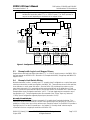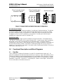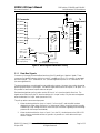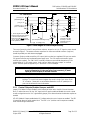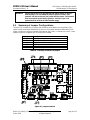
1
PMDX-122
Bi-Directional Break-Out Board
User’s Manual
Document Revision:
Date:
PCB Revision:
Serial Numbers:
PMDX
9704-D Gunston Cove Rd
Lorton, VA 22079-2366 USA
PMDX-122_Manual_111.doc
24 June 2009
1.11
24 June 2009
PCB-450B and PCB-450C
23110 and above
Web:
Phone:
FAX:
http://www.pmdx.com
+1 (703) 372-2975
+1 (703) 372-2977
©2005-2009, Practical Micro Design, Inc.
All Rights Reserved
Page 1 of 32
PMDX-122 User’s Manual
Document Revision: 1.11
PCB Revision: PCB-450B and PCB-450C
Serial Numbers: 23110 and above
Table of Contents
1.0
Overview .................................................................................................................................3
1.1
Important Safety Information ........................................................................................................................ 3
1.2
Warranty Summary......................................................................................................................................... 3
1.3
Trademarks ....................................................................................................................................................... 3
1.4
Features ............................................................................................................................................................. 4
1.5
Differences Between the PMDX-122 and the PMDX-121 ..................................................................... 4
1.6
Updates to this Manual................................................................................................................................... 4
2.0
Quick Setup Guide .................................................................................................................5
2.1
Example with Mach2/3, Charge Pump and Gecko Drivers..................................................................... 5
2.2
Example with Mach2/3, Charge Pump and PMDX-150 Stepper Drivers............................................. 6
2.3
Example with Logic Level Stepper Drivers ................................................................................................ 7
2.4
Example Limit Switch Wiring ........................................................................................................................ 7
3.0
Functional Description and Block Diagrams .......................................................................8
3.1
Data Bus ............................................................................................................................................................ 8
3.1.1
Data Bus Signals ...................................................................................................................................... 9
3.1.2
Data Bus Common...............................................................................................................................10
3.1.3
Data Bus Buffer Enable ........................................................................................................................10
3.1.4
Data Bus Buffer Direction ..................................................................................................................11
3.2
Control Outputs............................................................................................................................................11
3.2.1
Control Outputs Enabled Jumper and LED ....................................................................................12
3.2.2
General Purpose Outputs and LEDs ................................................................................................13
3.2.3
Pin 17 Output........................................................................................................................................13
3.2.4
Relay Control and LED (pin 1) ..........................................................................................................14
3.3
Status Inputs....................................................................................................................................................14
3.4
Fault and E-Stop Inputs.................................................................................................................................15
3.4.1
Fault Input...............................................................................................................................................17
3.4.2
E-Stop Input ...........................................................................................................................................17
3.4.2.1 E-Stop Input as “E-Stop” Signal .....................................................................................................17
3.4.2.2 E-Stop Input as General-Purpose Input .......................................................................................17
3.4.2.3 “E-Stop” LED (DS10) ......................................................................................................................18
3.5
Charge Pump (watchdog) ............................................................................................................................18
3.6
Power Supply Connections .........................................................................................................................18
4.0
Summary of Connector Pinouts .........................................................................................19
4.1
Data Bus Connectors (J1, J2, J3, and J4) ...................................................................................................19
4.2
Status Input Connector (J5) ........................................................................................................................20
4.3
Fault and E-Stop Connector (J6) ................................................................................................................21
4.4
Relay Contact Connector (J7) ....................................................................................................................21
4.5
Control Output Connector (J8).................................................................................................................21
4.6
PC Parallel Port Connectors (J10 & J9) ....................................................................................................22
4.7
Power Supply Connector (J11)...................................................................................................................23
4.8
USB Connector (J12) ....................................................................................................................................23
5.0
Summary of Jumper Configurations ..................................................................................24
6.0
Summary of LEDs ................................................................................................................27
7.0
Advanced Configurations ....................................................................................................28
7.1
Configuring a PMDX-122 to Emulate a PMDX-121...............................................................................28
7.2
Example Daisy-Chain PMDX-122 with Encoder Inputs ........................................................................28
8.0
Mechanical Specifications ....................................................................................................30
9.0
Electrical and Environmental Specifications .....................................................................31
Appendix A – Warranty..................................................................................................................32
PMDX-122_Manual_111.doc
24 June 2009
©2005-2009, Practical Micro Design, Inc.
All Rights Reserved
Page 2 of 32
PMDX-122 User’s Manual
PCB Revision: PCB-450B and PCB-450C
Serial Numbers: 23110 and above
Document Revision: 1.11
1.0
Overview
This document describes the configuration and operation of the PMDX-122 Bi-Directional Break-Out
Board. The PMDX-122 provides an interface between a PC and a multi-axis stepper motor system or
other user equipment. This document pertains to the following versions of the PMDX-122:
Circuit Board Revision:
Serial Number Range:
1.1
PCB-450B and PCB-450C (marked on the bottom of the board)
23110 and above
Important Safety Information
The PMDX-122 is intended for integration by the purchaser into industrial control systems. It is solely
the purchaser's responsibility to assure that the system is configured in a manner consistent with
applicable safety requirements. Practical Micro Design, Inc. does not control how this board is integrated
into the purchaser's system and cannot be responsible for guaranteeing the safety of your system.
The PMDX-122 is not guaranteed to be fail-safe. The system into which the PMDX-122 is installed should
provide fail-safe protection and emergency stop capability.
The PMDX-122 contains circuitry that may be connected to dangerous voltages. Care must be taken that
user cannot come in contact with these voltages. An enclosure that allows for modest ventilation, but
prevents intrusion by operator’s hands and foreign objects, especially conductive byproducts of machining
operations, should be utilized with this board. Interlock switches on power circuits should remove
power when the enclosure is opened.
Automated machine tools, into which the PMDX-122 may be integrated, can cause injury. Precautions
should be taken to assure that operators are trained in their proper operation and safety procedures, and
that they are protected from moving parts that may be under remote control and may move
unexpectedly.
This product may not be used in life support or other critical safety applications.
1.2
Warranty Summary
The PMDX-122 is warranted against failure due to defective parts or workmanship for 90 days from the
date of sale. Refer to Appendix A for complete warranty details.
If you have an item requiring service, please see the support page on the PMDX web site
(http://www.pmdx.com) for return instructions.
The purchaser must pay shipping to return the unit to PMDX. We will ship the repaired unit back to you
via ground transportation at our expense. Repairs are normally completed within 10 business days. See
Appendix A for our complete warranty details.
1.3
Trademarks
The following product names used in this manual are the trademark, tradename or registered mark of the
respective companies:
Product Names
G201, G202, G210, G212, G320, G340
and Geckodrive
Company
Geckodrive, Inc. (http://www.geckodrive.com)
Mach2 and Mach3 (note that this
document uses “Mach2/3” to refer to
either ‘Mach2” or “Mach3”)
ArtSoft Software Inc. (http://www.machsupport.com)
PMDX-121, PMDX-122, PMDX-150
PMDX/Practical Micro Design, Inc. (http://www.pmdx.com)
PMDX-122_Manual_111.doc
24 June 2009
©2005-2009, Practical Micro Design, Inc.
All Rights Reserved
Page 3 of 32
PMDX-122 User’s Manual
PCB Revision: PCB-450B and PCB-450C
Serial Numbers: 23110 and above
Document Revision: 1.11
1.4
Features
The PMDX-122 has the following features:
PC Parallel Port:
• Buffers signals to/from the PC parallel port
•
Allows use of all 8 data bits, 4 control
outputs and 5 status inputs
•
Centronics cable connector uses standard
PC printer cable
Status Inputs:
• 5 each status inputs w/pull-up resistors
•
Status signals are buffered
• LED indicators for each input
Relay Contact Outputs:
• Isolated relay with N.O and N.C terminals
• LED indicator for relay state
General Purpose Outputs:
• 3 each general purpose digital outputs
•
Outputs are buffered
•
LED indicator for each output
Power Supply Input:
• +7 to +12 VDC or 9 VAC input via 2.1mm
coaxial jack
•
Or alternate +5V DC via USB connector
•
Or alternate +7 to +12 VDC or 9 VAC
input via J8 screw terminal connector
•
Or alternate Regulated +5V DC +/- 5% via
J5 or J8 screw terminal connectors
Data Bus (Step/Direction signals):
• 4 axes of step and direction or 8 general
purpose signals
•
Data bus signals are buffered
•
Supports signals up to 1 MHz
•
Bi-directional data bus (outputs or inputs)
•
Can supply +5V to motor driver optocouplers or a ground reference for logic
inputs
Special Features:
• Wire clamp screw terminals for all
connections to data bus signals, relay and
control outputs, and status inputs
•
1.5
Auxiliary +5 volt supply output
Differences Between the PMDX-122 and the PMDX-121
The PMDX-122 is a replacement (and upgrade) to the PMDX-121 board. For directions on configuring
the PMDX-122 to function like a PMDX-121, see section 7.1. The differences between the PMDX-121
and PMDX-122 are:
•
The PMDX-122 supports bi-directional data on J1, J2, J3 and J4 (the PC parallel port’s data bus). The
PMDX-121 only supported “output from the PC”.
•
The PMDX-122’s data outputs (on J1, J2, J3 and J4) always have pull-up resistors. The PMDX-121’s
data outputs could have pull-up or pull-down resistors depending on the how JP1 was configured.
•
The PMDX-122 supports using the E-Stop input as a general-purpose input without affecting the data
and control outputs (see section 3.4.2.2). On the PMDX-121, the E-Stop input always affected the
data and control outputs.
•
The PMDX-122 supports daisy-chaining from another PMDX-122 or a PMDX-121, with the “charge
pump” on the first board able to disable the data and control outputs on the daisy-chained
PMDX-122 board (see section 7.2 for an example). The PDMX-121 did not support this feature.
1.6
Updates to this Manual
Check the PMDX web site for revisions or updates to this manual (http://www.pmdx.com). The latest
revision of this manual is available on the PMDX-122 page (follow the links from the main page).
PMDX-122_Manual_111.doc
24 June 2009
©2005-2009, Practical Micro Design, Inc.
All Rights Reserved
Page 4 of 32
PMDX-122 User’s Manual
Document Revision: 1.11
2.0
PCB Revision: PCB-450B and PCB-450C
Serial Numbers: 23110 and above
Quick Setup Guide
See section 3.6 for information on power sources and power connections for the PMDX-122.
2.1
Example with Mach2/3, Charge Pump and Gecko Drivers
Figure 1 on page 6 shows a standard configuration using Mach2 (or Mach3) software on the PC driving the
PMDX-122. The PMDX-122 is in turn connected to opto-isolated stepper drivers, such as the
Geckodrive units, that require a voltage source on their “common” terminal (see note below). Not all
opto-isolated stepper drivers require a voltage source on their “common” terminal. Verify they
style of opto-couplers on your stepper drivers before connecting them to the PMDX-122. The
PMDX-150, for example, requires a ground on the “common” terminal (see section 2.2).
NOTE – Some Geckodrive models require the use of +5V on their “common” terminal (G201,
G202 and G320, for example), while other models provide a jumper to select either
+5V or ground as the “common” reference (G210, G212, G340, for example). We
recommend always using “+5V” for the “common” reference on Geckodrive models.
This configuration takes advantage of Mach2/3’s “charge pump” facility so that the PMDX-122 disables all
of its outputs if the PC stops “behaving properly” (i.e. servicing the charge pump). Mach 2/3 must be set
to provide the step and direction signals to the data port pins that match your wiring configuration. We
recommend the connections as shown in Figure 1, and listed in Table 1. Mach 2/3 must also be set to run
the charge pump signal on pin 17. If you do not wish to use the charge pump feature, change jumper JP3
to the “not EStop/Fault” position.
The significant jumpers for this configuration are JP1, JP2, JP3 and JP5. The other jumpers (JP4 and JP6)
may be changed to suit your application. As configured in Figure 1, the Fault input defaults to “no fault”
and may be left unconnected if not used. To activate the Fault input, connect it to ground (not shown).
PC Parallel Port Pin #
2
3
4
5
6
7
8
9
Function
X axis Direction
X axis Step
Y axis Direction
Y axis Step
Z axis Direction
Z axis Step
A axis Direction
A axis Step
Table 1 – Mach2/3 Step and Direction Configuration
WARNING:
Do not use this configuration with non-isolated stepper drivers. Doing so
may damage the stepper drivers and the PMDX-122. For non-isolated
drivers see section 2.2.
PMDX-122_Manual_111.doc
24 June 2009
©2005-2009, Practical Micro Design, Inc.
All Rights Reserved
Page 5 of 32
PMDX-122 User’s Manual
PCB Revision: PCB-450B and PCB-450C
Serial Numbers: 23110 and above
Document Revision: 1.11
normal
J10
JP6
J11
J12
E-Stop Mode
signal only
J6
PWR
Alt In
E-Stop
fault
E-Stop
J9
GND
pin17
normal
pin17out
"OK"
J5+5V
JP4
always
pin 2-9 enable
OK
out JP2
DIR
**
JP5
pin16
pin14
+5V AUX OUT
AUX
OUT
J8
pin11
E-Stop switch
(normally closed)
or jumper wire
GND
pin12
JP1
pin13
pin15
GND
JP3
+5V
pin 2-9 COM
GND
pin2 pin3 COM
J1
not EStop/fault
Outputs Enabled
pin4 pin5 COM
J2
J7
J4
COMMON
or +5VDC
STEP
GECKODRIVE
DIR
COMMON
or +5VDC
STEP
DIR
COMMON
or +5VDC
STEP
GECKODRIVE
RLY
COM
N/O
pin8 pin9 COM
pin6 pin7 COM
J3
DIR
COMMON
or +5VDC
STEP
DIR
GECKODRIVE
N/C
CP-OK & not EStop/fault
GECKODRIVE
Figure 1 - Configuration w/Mach2/3, charge pump and Gecko stepper motor drivers
2.2
Example with Mach2/3, Charge Pump and PMDX-150 Stepper Drivers
Figure 2 shows a standard configuration using Mach2 (or Mach3) software on the PC driving the
PMDX-122. The PMDX-122 is in turn connected PMDX-150 stepper drivers, which have opto-couplers
that require a ground reference on their “common” terminal. Not all opto-isolated stepper drivers
require a ground reference on their “common” terminal. Verify they style of opto-couplers on
your stepper drivers before connecting them to the PMDX-122.
This configuration takes advantage of Mach2/3’s “charge pump” facility so that the PMDX-122 disables all
of its outputs if the PC stops “behaving properly” (i.e. servicing the charge pump). Mach 2/3 must be set
to provide the step and direction signals to the data port pins that match your wiring configuration. We
recommend the connections as shown in Figure 2, and listed in Table 1 (on page 5). Mach 2/3 must also
be set to run the charge pump signal on pin 17. If you do not wish to use the charge pump feature,
change jumper JP3 to the “not EStop/Fault” position.
The significant jumpers for this configuration are JP1, JP2, JP3 and JP5. The other jumpers (JP4 and JP6)
may be changed to suit your application.
As configured in Figure 2, the Fault input defaults to “no fault” and may be left unconnected if not used.
To activate the Fault input, connect it to ground. When using PMDX-150 stepper drivers, connect their
“Fault” outputs together and connect that to the PMDX-122’s Fault input as shown. This allows the fault
output of any PMDX-150 to disable the other PMDX-150 drivers, disable the PMDX-122’s outputs and
signal the fault to the PC via pin 10 (the ~Ack signal).
PMDX-122_Manual_111.doc
24 June 2009
©2005-2009, Practical Micro Design, Inc.
All Rights Reserved
Page 6 of 32
PMDX-122 User’s Manual
PCB Revision: PCB-450B and PCB-450C
Serial Numbers: 23110 and above
Document Revision: 1.11
NOTE – This configuration should also be used for stepper drivers that have logic level step
and direction inputs (also called “TTL” or “CMOS” inputs). The “Fault” input may or
may not be used, depending on the features of the stepper drivers.
normal
J10
JP6
J11
J12
E-Stop Mode
signal only
J6
PWR
Alt In
fault
E-Stop
GND
E-Stop
J9
GND
pin17
JP4
normal
pin17out
"OK"
J5+5V
always
pin 2-9 enable
OK
out JP2
DIR
**
JP5
pin16
pin14
+5V AUX OUT
AUX
OUT
J8
pin11
E-Stop switch
(normally closed)
or jumper wire
pin12
JP1
pin13
pin15
GND
not EStop/fault
Outputs Enabled
CP-OK & not EStop/fault
JP3
+5V
pin 2-9 COM
GND
pin2 pin3 COM
J1
pin4 pin5 COM
RLY
COM
N/O
pin8 pin9 COM
pin6 pin7 COM
J2
J3
COMMON
Fault*
STEP
PMDX-150
DIR
COMMON
Fault*
STEP
PMDX-150
J7
J4
DIR
COMMON
Fault*
STEP
DIR
COMMON
Fault*
STEP
DIR
PMDX-150
N/C
PMDX-150
Figure 2 - Configuration w/Mach2/3, charge pump and PMDX-150 stepper drivers
2.3
Example with Logic Level Stepper Drivers
Stepper drivers with logic level inputs (also called “TTL” or “CMOS” inputs) connect to the PMDX-122 in
the same manner as the PMDX-150. See section 2.2, Example with Mach2/3, Charge Pump and PMDX-150
Stepper Drivers.
2.4
Example Limit Switch Wiring
Mechanical switches, in either “normally open” or “normally closed” configurations, or optical interrupter
switches can be used to provide input signals to the PMDX-122. These switches can act as limit switches,
home indicators or other status information. Since the PMDX-122 provides pull-up resistors on the
status inputs (see section 3.3), mechanical switches can be wired directly to the signal pins on J5 and
ground. Optical interrupter switches require a current-limit resistor for the emitter LED. Note that the
examples below show the signals connected to “pin 11”. The input signals may be connected to any of
the signal pins on J5. The input signals may also be connected to the “E-Stop” input on J6 when the
“E-Stop” input is configured as a general-purpose input (see section 3.4.2.2).
Normally Closed Switches
The left-hand drawing in Figure 3 shows an example of “normally closed” mechanical switches. The
switches are wired in series so that the “normal” case is ground (logic low) going into pin 11 of the PC’s
parallel port. When one or more of the switches open, the pull-up resistor on the PMDX-122 provides a
logic high into pin 11 on the PC’s parallel port. Any number of “normally closed” switches may be
connected in series to a single input terminal on the PMDX-122.
PMDX-122_Manual_111.doc
24 June 2009
©2005-2009, Practical Micro Design, Inc.
All Rights Reserved
Page 7 of 32
PMDX-122 User’s Manual
Document Revision: 1.11
Three "normally closed"
switches in series.
J5+5V
PCB Revision: PCB-450B and PCB-450C
Serial Numbers: 23110 and above
Three "normally open"
switches in parallel.
Optical Interrupter
J5+5V
AUX
OUT
pin11
AUX
OUT
pin11
pin12
pin12
pin13
pin13
pin15
pin15
GND
GND
J5+5V
AUX
OUT
pin11
pin12
pin13
pin15
GND
Fairchild H21A1
or equivalent
Figure 3 – Example Switch and Optical Interruptor Configurations
Normally Open Switches
The center drawing in Figure 3 shows an example of “normally open” mechanical switches. The switches
are wired in parallel so that the “normal” case is +5V (logic high) going into pin 11 of the PC’s parallel
port (due to the pull-up resistor on the PMDX-122). When one or more of the switches close, a logic
low appears on pin 11 on the PC’s parallel port. Any number of “normally open” switches may be
paralleled onto a single input terminal on the PMDX-122.
Optical Interrupter
The right-hand drawing in Figure 3 shows an example of an optical interrupter. This example uses the
“+5V Aux Out” from the PMDX-122 to power the emitter LED. Choose a resistor value to provide the
desired LED current (refer to the data sheet for the optical interrupter). The output transistor is
connected as an “open collector” output between the PMDX-122 input pin and ground. When light from
the LED strikes the sensor transistor, the transistor conducts giving a logic low on pin 11 of the PC’s
parallel port. Then the LED is “interrupted”, the transistor stops conducting and the PMDX-122’s pull-up
resistor gives a logic high on pin 11.
3.0
Functional Description and Block Diagrams
3.1
Data Bus
The PC parallel port contains an 8-bit data bus. On older PCs, this data bus was “output only.” On
newer PCs, the data bus is bi-directional and can switch from “output” to “input” under software control.
The PMDX-122 buffers the data bus signals between the PC and the PMDX-122’s connectors J1 through
J4. The PMDX-122 supports the bi-directional data bus, where the PMDX-122’s data direction is jumper
selectable to “output only”, “input only” or “controlled by the ‘~Select In’ control signal.” See section 4.1
for more information on the data bus connectors.
PMDX-122_Manual_111.doc
24 June 2009
©2005-2009, Practical Micro Design, Inc.
All Rights Reserved
Page 8 of 32
PMDX-122 User’s Manual
PCB Revision: PCB-450B and PCB-450C
Serial Numbers: 23110 and above
Document Revision: 1.11
+5V
PC Connector
1
2
pin 9 (Data7)
3
pin 8 (Data6)
2.2K
pin 7 (Data5)
pin 6 (Data4)
Buffer
pin 5 (Data3)
8
pin 4 (Data2)
8
pin 3 (Data1)
+5V
1-2 = "Out"
"Open" = "In"
2-3 = "Auto"
pin 17
(Slct In)
1 JP5
2
Enable
Direction
pin 2 (Data0)
JP1
To
Equipment
COM
pin 9
pin 8
J4
COM
pin 7
pin 6
J3
COM
pin 5
pin 4
J2
COM
pin 3
pin 2
J1
Always On
3
1
2
10K
High = Output (from PC)
Low = Input (to PC)
JP2
3
OK
(from EStop/Fault/Charge Pump)
Figure 4 - Block diagram of Data Bus Circuitry
3.1.1 Data Bus Signals
Connectors J1 through J4 contain buffered versions of the PC parallel port “data bus” signals. These
connectors are labeled to denote which pin on the PC’s parallel port 25-pin “D” connector is associated
with each terminal. “Pin 2” is data bus bit “D0” (the least-significant bit) and “Pin 9” is data bus bit “D7”
(the most-significant bit).
The data bus signals are normally used for step and direction outputs. However, they can also be used as
general-purpose output or input signals. The data bus signals must be either all outputs, or all inputs. It is
not possible to have some as outputs and some as inputs.
Each data bus signal has a pull-up resistor and an LED that is “on” when the signal is driven low. The
signals can be driven low by the PC when the data bus is in “output” mode, or by the external equipment
when the data bus is in “input” mode (see section 3.1.4).
The pull-up resistors serve several purposes:
1.
When the data bus direction is set to “output” (i.e. from the PC), and the buffer has been
disabled via the E-Stop input, Fault input or a “charge pump” failure, the pull-up resistors provide
a default logic “high” voltage level at the connectors (see note below regarding the actual voltage
present when then outputs are disabled).
2.
When the data bus direction is set to “input” (i.e. to the PC), the data inputs to the PMDX-122
can be driven by mechanical switches to ground or by encoders or other devices with opencollector outputs.
PMDX-122_Manual_111.doc
24 June 2009
©2005-2009, Practical Micro Design, Inc.
All Rights Reserved
Page 9 of 32
PMDX-122 User’s Manual
Document Revision: 1.11
3.
PCB Revision: PCB-450B and PCB-450C
Serial Numbers: 23110 and above
When the data bus direction is set to “input” (i.e. to the PC), the pull-up resistors provide a
default logic “high” input voltage to the PMDX-122’s data bus buffer when there is no signal
source driving that data signal from the connectors.
Note that the voltage present on J1 through J4 when the buffer is tri-stated is approximately 3.2V. This is
due to the voltage drop across the protection diode and the LED.
3.1.2 Data Bus Common
The PMDX-122 provides a common reference signal on the four data bus connectors (J1, J2, J3 and J4).
This common signal is the same for all four connectors and is jumper selectable between a nominal +5V
or ground. Jumper JP1 (labeled “pin 2-9 COM” on the circuit board) determines this voltage reference as
follows:
Setting
1 to 2
2 to 3
Label
Description
+5V
Supplies an nominal +5V to the common terminals on J1, J2, J3 and J4. This
configuration is commonly used when the motor drivers have optically isolated
inputs that expect a voltage source on their “common” terminal (such as some of
the Geckodrive modules). In this case, the PMDX-122 supplies the +5V power to
the opto-couplers. See the note and warning below.
GND
Connects the PMDX-122’s ground to the common terminals. This setting would
typically be used with motor drivers that have optically isolated inputs that expect a
ground reference on their “common” terminal (such as the PMDX-150). It can also
be used with motor drivers or general-purpose logic signals that have non-isolated,
TTL or CMOS logic style inputs.
Table 2 – “Pin 2-9 Common” Jumper Settings (JP1)
The PMDX-122 has a protection diode between its +5V supply and the common terminals (see Figure 4).
This prevents any voltages that are accidentally applied to the common terminals from damaging the
PMDX-122. A side effect of this diode is that the “+5V” that appears on the common terminals is less
than +5V. The actual voltage depends on the PMDX-122’s power source. For AC or DC power via J11,
the voltage is approximately 4.2V. When using the USB connector for power, the voltage may be slightly
lower than 4.2V, depending on several factors, including length of the USB cable and total load on the USB
hub (see sections 4.8 and 9.0 for USB hub requirements). These voltages are sufficient to drive external
opto-isolators.
WARNING:
When connecting to non-isolated motor driver inputs you must use the
“ground” setting on jumper JP1. Do not connect the PMDX-122’s “+5V”
reference to ground on the motor driver module. Doing so may damage the
buffers on the PMDX-122 and the inputs to the motor drivers.
NOTE – Changing the common reference from “+5V” to “Gnd” (via jumper JP1) when feeding
optically isolated driver inputs has the effect of inverting the step and direction signals.
3.1.3 Data Bus Buffer Enable
The PMDX-122 allows the E-Stop, Fault and charge pump circuits to disable the data bus buffers. Jumpers
JP2 and JP3, determine if and when the data bus buffers will be disabled. Section 3.1.1, Data Bus Signals,
describes behavior of the data bus signals when they are disabled. See section 3.2.1 for information on
configuring jumper JP3. Jumper JP2 is labeled “pin 2-9 enable” on the circuit board, and can be configured
as follows:
PMDX-122_Manual_111.doc
24 June 2009
©2005-2009, Practical Micro Design, Inc.
All Rights Reserved
Page 10 of 32
PMDX-122 User’s Manual
Document Revision: 1.11
PCB Revision: PCB-450B and PCB-450C
Serial Numbers: 23110 and above
Setting
Label
Description
1 to 2
always
The data bus buffers are always enabled (i.e. ignore the E-Stop, Fault and charge
pump circuits)
2 to 3
OK
Data bus buffers are enabled as long as the “Outputs Enabled” LED is “on”. Note
that this setting uses the “OK’ signal from jumper JP3 (see section 3.2.1, Control
Outputs Enabled Jumper and LED for more information).
Table 3 – “Pin 2-9 Enable” Jumper Settings (JP2)
3.1.4 Data Bus Buffer Direction
Jumper JP5 determines the direction of the PMDX-122’s data bus buffer. The data bus is configured as
input or output for the entire data bus. The direction of individual bits cannot be controlled.
Setting
Label
1 to 2
out
The data buffers are configured as “output” buffers (from the PC out through the
PMDX-122).
**
The data buffer direction is dynamically controlled by the “~Select In” signal from
the PC’s parallel port (pin 17 on the 25-pin “D” connector) as follows:
Logic High
Data buffers are “output” (from the PC)
Logic Low
Data buffers are “input” (to the PC)
Note that the “~Select In” signal also drives the “charge pump” function. If you
are using “~Select In” for direction control, make sure to disable the charge pump
function (see section 3.2.1). See the note and warning below.
2 to 3
Open
(jumper
not
installed)
Description
The data buffers are configured as “input” buffers (through the PMDX-122 into
the PC). See the note and warning below.
Table 4 – Data Bus Direction Jumper Settings (JP5)
WARNING:
When jumper JP5 is configured so that the data bus direction is either
“input” or “~Select In” controlled, jumper JP2 should be set to “always
enabled”. There are no pull-up or pull-down resistors on the PC side of the
data bus buffers. If the data buffers are configured as “input to PC” and
then disabled, the PC’s parallel port will have floating inputs which could
result in erratic readings.
NOTE – In order to use the data lines as inputs to a PC, the PC’s BIOS must be set so that the
parallel port is configured as either “bi-directional”, “EPP” or “ECP”. Please consult
your PC’s documentation for instructions on how to change your BIOS settings.
3.2
Control Outputs
The PMDX-122 supports three general-purpose control outputs, as shown in Table 17 on page 21. The
fourth PC parallel port control signal (~Strobe) is dedicated to the PMDX-122’s on-board relay (see
section 3.2.4). Figure 5 shows a block diagram of the control outputs.
PMDX-122_Manual_111.doc
24 June 2009
©2005-2009, Practical Micro Design, Inc.
All Rights Reserved
Page 11 of 32
PMDX-122 User’s Manual
PCB Revision: PCB-450B and PCB-450C
Serial Numbers: 23110 and above
Document Revision: 1.11
To relay
PC Connector
(~AutoFeed) pin 14
(~Init) pin 16
(~Selelct In) pin 17
(see ** note below)
2
10K
"OK"
3
**
**
**
**
Buffer
Enable
*
*
*
JP4
**
1 "normal"
(~Strobe) pin 1
2.2K
+5V
* All four signals from the PC
have their own pull-down resistor.
** Serial number 24242 and
above have 10K pull-up on the
"pin 17" signal, older boards have
a 10K pull-down resistor.
OK
(from EStop/Fault/Charge Pump)
To charge pump
+5V
J8
+5V Aux
pin 14
**
**
**
pin 16
pin 17
Pwr Alt. In
To
10K power
GND
supply
** All four signals
have their own LED.
All except "~Strobe"
have their own pulldown resistor
Figure 5 - Block diagram of Control Output Circuitry
The control inputs from the PC have pull-down resistors, except for the “pin 17” signal on newer boards
as noted in Figure 5. This ensures a known output level on the screw terminal connector (logic low)
should the parallel port cable become unplugged.
Connector J8 also provides an auxiliary +5V output (which can also be a regulated +5V input, see section
3.6), ground reference, and an alternate power supply input. The +5V output can be used to power
external opto-couplers. The “PWR Alt In” terminal provides a screw-terminal alternative to J11 for
connecting an AC or DC power source. It also can be a “daisy-chain power output” to a second
PMDX-122 when power is supplied on J11. See section 7.2 for an example.
WARNING:
When using the “Aux. Power In” on J8 pin 5, make sure that no power
source is connected to J11 (the coax power input connector), J5 (status
inputs) J8 (control outputs) or the USB connector.
NOTE – Due to logic inside the PC, some control outputs are inverted. This means that that
writing a “1” to a bit in the control register may result in a logic “low” at the 25-pin
“D” connector. Please refer to technical documentation on the PC parallel port or
your control software for more information.
3.2.1 Control Outputs Enabled Jumper and LED
Jumper JP3 is labeled “Outputs Enabled” and is located just below and to the left of the serial number
block. It selects the source for the “OK” signal, which is used to enable and disable the control outputs
as well as a signal source the “OK” signal used by jumper JP2 to determine when the data bus outputs are
enabled.
LED DS1 (labeled “Outputs enabled when lit”) indicates when the control outputs are enabled. The LED
is located just above the serial number block. The LED is “on” (and the control outputs are enabled)
under the following circumstances:
PMDX-122_Manual_111.doc
24 June 2009
©2005-2009, Practical Micro Design, Inc.
All Rights Reserved
Page 12 of 32
PMDX-122 User’s Manual
Document Revision: 1.11
•
•
•
PCB Revision: PCB-450B and PCB-450C
Serial Numbers: 23110 and above
The Fault input is driven (or allowed to float) high (inactive), see section 3.4.1
And, optionally, if the E-Stop input is driven low and jumper JP6 is configured in “normal” mode (see
section 3.4.2). If jumper JP6 is configured to any other setting, the E-Stop input does not affect the
control outputs.
And, optionally, when the charge pump circuit is “OK” and jumper JP3 is configured in “CP-OK and
not EStop/Fault” mode. If jumper JP3 is configured to “not EStop/Fault” then the charge pump is
ignored and has no effect on the control outputs.
NOTE –
The “Outputs enabled when lit” LED does not necessarily indicate when the data bus
outputs are enabled. That depends on the setting of jumper JP2 (see section 3.1.3).
Setting
Label
Description
1 to 2
not
EStop/fault
Control outputs are enabled (and the “OK” signal is asserted) when the Fault
signal is NOT asserted, and optionally when the E-Stop signal is NOT asserted
(depends on jumper JP6, see section 3.4.2). The charge pump circuit is ignored.
2 to 3
CP-OK
& not
EStop/fault
Control outputs are enabled (and the “OK” signal is asserted) when the charge
pump circuit is OK and Fault signal is NOT asserted, and optionally when the
E-Stop signal is NOT asserted (depends on jumper JP6, see section 3.4.2).
Table 5 – “Outputs Enabled” Jumper Settings (JP3)
3.2.2 General Purpose Outputs and LEDs
Three of the control signals are available as general-purpose outputs: pins 14, 16 and 17 (note that pin 17
is a special case with additional functionality, see section 3.2.3). The “Control Output” LEDs are located
next to connector J8, just above each of the pin number labels (“pin 14”, “pin 16”, and “pin 17”). Each
LED is “on” when the corresponding output signal is driven high.
Each control output has a 10K ohm pull-down resistor. This provides a logic low level whenever the
control output buffer is disabled. Note that this is a fairly weak pull-down, and can be overridden
externally with a stronger pull-up resistor if required.
3.2.3 Pin 17 Output
In addition to being available as a general-purpose output, the “pin 17” signal serves several additional (and
optional) functions:
• Drives the charge pump circuit (see section 3.5). While pin 17 always drives the charge pump, the
output of the charge pump may be ignored, depending on the setting of jumper JP3 (see section 3.2.1)
• Optionally, determines the direction of the data bus (depends on jumper JP5, see section 3.1.4)
• Optionally acts as a daisy-chain output of the fault/E-Stop/charge pump status, depending on the
configuration of jumper JP4 (see the table below).
Jumper JP4 is labeled “pin 17 out” and selects the source for the “pin 17” signal on connector J8.
PMDX-122_Manual_111.doc
24 June 2009
©2005-2009, Practical Micro Design, Inc.
All Rights Reserved
Page 13 of 32
PMDX-122 User’s Manual
Document Revision: 1.11
PCB Revision: PCB-450B and PCB-450C
Serial Numbers: 23110 and above
Setting
Label
Description
1 to 2
normal
Pin 17 from the PC parallel port drives the “pin 17” control output on J8 as well
as the charge pump circuitry and possibly the data bus direction control
(depending on the setting of jumper JP5, see section 3.1.4).
OK
Pin 17 from the PC parallel port drives only the charge pump circuitry (and
possibly the data bus direction control, see section 3.1.4). The “pin 17” control
output on J8 is driven “high” or floats low based on the state of the E-Stop and
Fault inputs, the “charge pump” circuit and jumpers JP3 and JP6. See sections
3.4.2, 3.4.1 and 3.5 for more information. This setting allows the charge pump
circuit to disable external drivers via opto-isolated relays and also allows daisychaining the fault/E-Stop/charge pump status to a second PMDX-122 (see section
7.2 for an example of daisy-chaining boards).
2 to 3
Table 6 – “Pin 17 Output Source” Jumper Settings (JP4)
3.2.4 Relay Control and LED (pin 1)
The “pin 1” control signal (“~Strobe”) is dedicated to the on-board relay. The “pin 1” LED is located next
to the relay contacts connector and indicates the state of the relay. The LED is “on” when the relay is
energized (connecting the “N/O” terminal with the “RLY COM” terminal). The LED is “off” when the
relay is de-energized (connecting the “N/C” terminal with the “RLY COM” terminal). A logic high on the
pin 1 input from the PC (~Strobe) energizes the relay. Table 16 on page 21 shows the pin-out for the
relay connector (J7).
NOTE – Due to logic inside the PC, the “~Stobe” control output (pin 1) is inverted. This
means that writing a “1” to the bit in the control register results in a logic “low” at
the 25-pin “D” connector. In order to energize the relay, a “0” must be written to
the parallel port control register. Please refer to technical documentation on the PC
parallel port or your control software for more information.
3.3
Status Inputs
Four of the status signals are available as general-purpose inputs: pins 11, 12, 13 and 15. The fifth status
input on the PC parallel port (pin 10, ~Ack) is connected to the Fault and E-Stop circuitry. See sections
3.4.2, E-Stop Input and 3.4.1, Fault Input, for more information on this signal. Figure 6 on page 15 shows a
block diagram of the status input circuitry.
The “Status Input” LEDs are located next to connector J5, just above each of the pin number labels
(“pin 11”, “pin 12”, “pin 13” and “pin 15”). Each LED is “on” when the corresponding input signal is
driven low.
Each status input has a 10K ohm pull-up resistor and an RC low-pass filter (to remove high-frequency
noise from the inputs). The pull-up resistor provides a logic high input level whenever the input terminal
is not driven by an external source. The inputs may be driven by open-collector drivers or mechanical
switches to ground, or to be left unconnected when not used. Note that this is a fairly weak pull-up, and
can be overridden externally with a stronger pull-down resistor if required.
NOTE – Due to logic inside the PC, some status inputs are inverted. This means that a logic
“high” output from the PMDX-122 to the PC’s parallel port is read as a “0” in the
status register. Please refer to technical documentation on the PC parallel port or
your control software for more information.
PMDX-122_Manual_111.doc
24 June 2009
©2005-2009, Practical Micro Design, Inc.
All Rights Reserved
Page 14 of 32
PMDX-122 User’s Manual
Document Revision: 1.11
PCB Revision: PCB-450B and PCB-450C
Serial Numbers: 23110 and above
+5V
2.2K
+5V
J5
PC Connector
+5V Aux
10K
(~Busy) pin 11
Buffer
(Paper End) pin 12
**
**
**
**
10K
10K
(Select Out) pin 13
10K
Enable
(~Error) pin 15
(~Ack) pin 10
pin 11
pin 12
pin 13
pin 15
GND
100pF
** All four signals each have their
Always
On
own LED and pull-up resistor
EStop
(from E-Stop and Fault circuit)
Figure 6 - Block diagram of Status Input Circuitry
3.4
Fault and E-Stop Inputs
The PMDX-122 provides both E-Stop (emergency stop) and Fault inputs. The operation of each input is
described in the following sections. The function of the E-Stop and Fault inputs depends on the
configuration of jumper JP6, as shown in Table 7 and the block diagrams below.
Setting
1 to 2
(Figure 7)
2 to 3
(Figure 8)
Open
(Figure 9)
Label
Description
normal
The E-Stop input is an emergency stop signal. The Fault input has a 100K pull-up
resistor so that its default state is “no fault”. The E-Stop and Fault inputs combine
to drive the “~Ack” signal (pin 10) into the PC parallel port and to optionally
disable buffers on the PMDX-122.
signal
only
The E-Stop input is a general-purpose input and directly drives the “~Ack” signal
(pin 10) into the PC parallel port without affecting the data bus and control
outputs on the PMDX-122 board. The Fault input has a 10K pull-down resistor
and a 100K pull-up resistor so that its default state is “fault”. This jumper setting
can be used for daisy-chaining two PMDX-122 boards, see section 7.2.
The E-Stop input is a general-purpose input and directly drives the “~Ack” signal
(pin 10) into the PC parallel port without affecting the data bus and control
outputs on the PMDX-122 board. The Fault input has a 100K pull-up resistor so
that its default state is “no fault” (i.e. the Fault input can be left unconnected if
not used).
Table 7 – E-Stop Mode Jumper Settings (JP6)
NOTE – When jumper JP6 is set to the “normal” setting, the Fault input must be allowed to
float high (or be driven high) in order for the output buffers to be enabled and for the
“~Ack” status signal to the PC parallel port to go low.
PMDX-122_Manual_111.doc
24 June 2009
©2005-2009, Practical Micro Design, Inc.
All Rights Reserved
Page 15 of 32
PMDX-122 User’s Manual
PCB Revision: PCB-450B and PCB-450C
Serial Numbers: 23110 and above
Document Revision: 1.11
+5V
+5V
+5V
2.2K
Wired-OR
9K
2.2K
1.0K
J6
Fault*
pin 10/E-Stop
GND
DS10
"EStop Active"
10K
EStop
(to status input circuit and then to
the PC parallel port ~Ack [pin 10]
signal)
+5V
Pin 17
(from PC parallel port)
Charge
Pump
1
2
3
AND
OK
(to control buffer enable
and data bus enable jumper
JP3)
JP3
Figure 7 – Fault, E-Stop and Charge Pump when JP6 set to “pins 1-2”
+5V
+5V
+5V
2.2K
100K
2.2K
1.0K
J6
Fault*
pin 10/E-Stop
GND
DS10
"EStop Active"
10K
EStop
(to status input circuit and then to the
PC parallel port ~Ack [pin 10] signal)
10K
+5V
1
2
Pin 17
(from PC parallel port)
Charge
Pump
3
AND
OK
(to control buffer enable and
data bus enable jumper JP3)
JP3
Figure 8 – Fault, E-Stop and Charge Pump when JP6 set to “pins 2-3”
+5V
+5V
+5V
2.2K
100K
2.2K
1.0K
J6
Fault*
pin 10/E-Stop
GND
DS10
"EStop Active"
10K
EStop
(to status input circuit and then to the
PC parallel port ~Ack [pin 10] signal)
+5V
Pin 17
(from PC parallel port)
Charge
Pump
1
2
3
AND
JP3
OK
(to control buffer enable and
data bus enable jumper JP3)
Figure 9 – Fault, E-Stop and Charge Pump when JP6 set to “open”
PMDX-122_Manual_111.doc
24 June 2009
©2005-2009, Practical Micro Design, Inc.
All Rights Reserved
Page 16 of 32
PMDX-122 User’s Manual
Document Revision: 1.11
PCB Revision: PCB-450B and PCB-450C
Serial Numbers: 23110 and above
3.4.1 Fault Input
The Fault input provides an interface for external fault detection circuits, such as the fault signals from the
PMDX-150 stepper motor drivers. This signal is “active low”, meaning that a logic “low” indicates a fault
condition, and a logic high means “all is OK”. Figure 7, Figure 8 and Figure 9 on page 16 shows block
diagrams of the Fault input circuitry for the various configurations of jumper JP6.
The Fault input can be connected to an external “wired-or” configuration of open-collector status signals
or mechanical switches to ground (switch closed means “fault”). All of the external fault signals should be
tied together and connected to the PMDX-122’s Fault input. Depending on the configuration of jumper
JP6, the Fault input has either a 100K ohm pull-up resistor or a 10K ohm pull-down resistor. See Table 7
on page 15.
When jumper JP6 is set to the “normal” setting, the E-Stop and Fault inputs are combined (logic “OR”) to
drive the “~Ack” status signal (pin 10) to the PC’s parallel port. Refer to section 3.4.2.1, E-Stop Input as
“E-Stop” Signal, for a list of actions that take place when the Fault input is driven low.
3.4.2 E-Stop Input
The E-Stop input has different functionality depending on the setting of jumper JP6, as described in the
following sections. Figure 7, Figure 8 and Figure 9 on page 16 shows block diagrams of the E-Stop input
circuitry for the various configurations of jumper JP6.
3.4.2.1
E-Stop Input as “E-Stop” Signal
When jumper JP6 set to the “normal” setting, the E-Stop input provides an interface for external
“emergency stop” circuits (see Figure 7). This signal is “active high”, meaning that a logic “high” tells the
system to stop, and a logic low means “all is OK”.
The E-Stop input is designed to be connected to an external “normally closed” switch (or group of
switches all wired in series). The external switch(es) should be wired between the E-Stop pin and ground,
such that the switch contacts open to signal an emergency stop condition. The PMDX-122 provides a
2.2K ohm pull-up resistor on the E-Stop input. This means that the external emergency stop circuit must
be capable of sinking 2.7 mA of current when the switch contacts are “closed”.
In this configuration, the E-Stop and Fault inputs are combined (logic “OR”) to drive the “~Ack” status
signal to the PC’s parallel port and to enable or disable the data bus and control output buffers.
NOTE – With jumper JP6 set to the “normal” setting (pins 1-2), the E-Stop signal must be
grounded (or driven low) in order for the data bus and control output buffers to be
enabled, and for the “~Ack” status signal to the PC parallel port to go low.
When either (or both) the E-Stop (active high) or Fault (active low) inputs are asserted, the following
actions take place:
• The ACK bit in the PC’s status register reads as a “1”
• The LED labeled “E-Stop active” (reference designator DS10, near J6) is “on”.
• The LED labeled “Outputs Enabled when lit” (reference designator DS1, near the center of the
board) is “off”
• The control outputs are tri-stated with a weak (10K ohm) pull-down
• The relay is de-energized
• The data bus outputs may be tri-stated with a 2.2K ohm pull-up, depending on the setting of jumpers
JP2 (see section 3.1.3) and JP5 (see section 3.1.4)
3.4.2.2
E-Stop Input as General-Purpose Input
When jumper JP6 set to “signal only” or “open”, the E-Stop input acts as a general-purpose input that
drives the “~Ack” status input on the PC parallel port without affecting the data bus and control outputs
PMDX-122_Manual_111.doc
24 June 2009
©2005-2009, Practical Micro Design, Inc.
All Rights Reserved
Page 17 of 32
PMDX-122 User’s Manual
Document Revision: 1.11
PCB Revision: PCB-450B and PCB-450C
Serial Numbers: 23110 and above
on the PMDX-122 (see Figure 8 and Figure 9). The signal is not inverted on by the PMDX-122. A logic
high on the E-Stop input is output as a logic high on the “~Ack” signal. When the E-Stop is used as a
general-purpose input, the Fault input can be set to default to either “active” or “inactive”. See section
3.4.1 for more information.
3.4.2.3
“E-Stop” LED (DS10)
The “E-Stop” LED is located next to connector J6, and is labeled “E-Stop active”. The LED indicates the
state of the “~Ack” signal to the PC (pin 10), which is driven by the E-Stop input and optionally by the
Fault input. The LED is “on” when the E-Stop input is high (active). If jumper JP6 is configured as
“normal”, then the LED will also be “on” when the Fault input is low (active). See sections 3.4.2, E-Stop
Input, and 3.4.1, Fault Input, for more information on these signals.
3.5
Charge Pump (watchdog)
The charge pump circuit (also called a watchdog circuit) is designed to disable the PMDX-122 control
outputs (and optionally the data bus outputs) when the software running on the PC stops working
properly. It does this by monitoring pin 17 on the PC parallel port (the “~Select In” signal). When this
signal is toggling between high and low, the charge pump is “OK”. When the “~Select In” signal stops
toggling, the charge pump is “not OK”. Depending on the configuration of jumpers JP3 and JP2, the
charge pump may cause the PMDX-122 to disable the output buffers when it is “not OK”. Jumper JP3
determines whether the output from the charge pump is used to enable and disable the control output
buffers (see section 3.2.1). Jumper JP2 determines whether the step and direction outputs are ever
disabled (see section 3.1.3). See also the block diagrams in section 3.4.
This charge pump circuit is designed to work with the Mach2/3 CNC software. However, any software
that can toggle pin 17 on the PC parallel port can make use of this feature. If your software does not
support this feature, configure the jumpers to disable the charge pump circuit.
NOTE – The state of the charge pump signal is not reflected in the E-Stop and Fault status that
is output on the “~Ack” signal to the PC (pin 10 on the parallel port). This is to
prevent “lock up” of the software. Mach2/3 CNC software requires that the
Emergency Stop signal (~Ack) not be asserted before it will start generating the
“charge pump” signal.
3.6
Power Supply Connections
The PMDX-122 may be powered from several different power sources.
WARNING:
I
Power Source
Unregulated
AC or DC
IUSB Power
Regulated
+5V DC
Only one of these power sources can be used at a time. Connecting a
power source to more than one of these power inputs may damage the
PMDX-122.
Voltage
9 VAC or +7 to +12 VDC
+5V DC
Regulated +5V DC +/- 5%
Connector
J11, a 2.1mm coaxial jack (see section 4.7)
-- or -J8 screw terminal connector pins 5 and 6
(see section 4.5)
J12, the USB connector (see section 4.8)
J5 screw terminal connector pins 1 and 6
(see section 4.2 and note below)
-- or -J8 screw terminal connector pins 1 and 6
(see section 4.5 and note below)
Table 8 – Summary of PMDX-122 Power Sources
PMDX-122_Manual_111.doc
24 June 2009
©2005-2009, Practical Micro Design, Inc.
All Rights Reserved
Page 18 of 32
PMDX-122 User’s Manual
Document Revision: 1.11
NOTE:
4.0
PCB Revision: PCB-450B and PCB-450C
Serial Numbers: 23110 and above
If using either connector J5 or J8 as an input for regulated +5V DC power to the
PMDX-122, the other connector may still be used as a +5V DC output, provided that
your regulated power supply can supply sufficient current for the PMDX-122
and any other devices you connect. For example, if you connect a regulated +5V
DC power source to J8 pins 1 and 6, you can still use J5 pins 1 and 6 as a +5V DC
power source for sensors, etc. In this case your regulated DC power supply must be
capable of supplying 200 mA plus the current required by your devices.
Summary of Connector Pinouts
The PMDX-122 contains several connectors, as listed in Table 9 below. Refer to the following tables for
details on the pin-outs for each connector. For all connectors, pin “1” is the pin closest to the reference
designator (i.e. J1 pin 1 is the pin closest to the “J1” text on the circuit board). In addition, all connectors
have square pads on pin 1 (look on the bottom of the circuit board).
Connector
J1, J2, J3, J4
J5
J6
J7
J8
J9
J10
J11
J12
Description
Data Bus Signals (can be step and direction)
Status Input Signals
Fault and E-Stop inputs
Relay contact outputs
Control Outputs
26-pin ribbon header (alternate connection to PC parallel port)
Centronics 36-pin PC Parallel Port
DC Power via a 2.1mm coax connector
USB Connector (used for power only)
Table 9 – Summary of PMDX-122 Connectors
4.1
Data Bus Connectors (J1, J2, J3, and J4)
The data bus connectors are labeled to denote which pin on the PC’s parallel port that is associated with
each connector pin. “Pin 2” is data bus bit “D0” (the least-significant bit) and “Pin 9” is data bus bit “D7”
(the most-significant bit).
Pin Number
Label
1
Pin 2
2
Pin 3
3
COM
Description
Buffered signal from pin 2 of the PC parallel port’s 25-pin “D” connector
(parallel port signal name “D0”)
Buffered signal from pin 3 of the PC parallel port’s 25-pin “D” connector
(parallel port signal name “D1”)
Common voltage reference, same for all four connectors (see section
3.1.2 for reference source)
Table 10 – Data Bus Connector Pin-Out (J1)
Pin Number
Label
1
Pin 4
2
Pin 5
3
COM
Description
Buffered signal from pin 4 of the PC parallel port’s 25-pin “D” connector
(parallel port signal name “D2”)
Buffered signal from pin 5 of the PC parallel port’s 25-pin “D” connector
(parallel port signal name “D3”)
Common voltage reference, same for all four connectors (see section
3.1.2 for reference source)
Table 11 – Data Bus Connector Pin-Out (J2)
PMDX-122_Manual_111.doc
24 June 2009
©2005-2009, Practical Micro Design, Inc.
All Rights Reserved
Page 19 of 32
PMDX-122 User’s Manual
Document Revision: 1.11
Pin Number
Label
1
Pin 6
2
Pin 7
3
COM
PCB Revision: PCB-450B and PCB-450C
Serial Numbers: 23110 and above
Description
Buffered signal from pin 6 of the PC parallel port’s 25-pin “D” connector
(parallel port signal name “D4”)
Buffered signal from pin 7 of the PC parallel port’s 25-pin “D” connector
(parallel port signal name “D5”)
Common voltage reference, same for all four connectors (see section
3.1.2 for reference source)
Table 12 – Data Bus Connector Pin-Out (J3)
Pin Number
Label
1
Pin 8
2
Pin 9
3
COM
Description
Buffered signal from pin 8 of the PC parallel port’s 25-pin “D” connector
(parallel port signal name “D6”)
Buffered signal from pin 9 of the PC parallel port’s 25-pin “D” connector
(parallel port signal name “D7”)
Common voltage reference, same for all four connectors (see section
3.1.2 for reference source)
Table 13 – Data Bus Connector Pin-Out (J4)
4.2
Status Input Connector (J5)
Connector J5 provides access to four of the five status input signals. The fifth status input on the PC
parallel port is connected to the Fault and E-Stop circuitry. See section 3.4.2, E-Stop Input, for more
information on this signal.
Pin Number
1
Label
+5V Aux Out
2
3
4
5
6
Pin 11
Pin 12
Pin 13
Pin 15
GND
Description
Auxiliary +5V output for external sensor power
OR regulated +5V DC input (see section 3.6)
Status input, buffered, to PC parallel port pin 11 (Busy)
Status input, buffered, to PC parallel port pin 12 (Paper End)
Status input, buffered, to PC parallel port pin 13 (Select Out)
Status input, buffered, to PC parallel port pin 15 (~Error)
Ground connection
Table 14 – Status Input Connector Pin-Out (J5)
NOTE – Due to logic inside the PC, some status inputs are inverted. This means that a logic
“high” output from the PMDX-122 to the PC’s parallel port is read as a “0” in the
status register. Please refer to technical documentation on the PC parallel port or
your control software for more information.
PMDX-122_Manual_111.doc
24 June 2009
©2005-2009, Practical Micro Design, Inc.
All Rights Reserved
Page 20 of 32
PMDX-122 User’s Manual
Document Revision: 1.11
4.3
PCB Revision: PCB-450B and PCB-450C
Serial Numbers: 23110 and above
Fault and E-Stop Connector (J6)
J6 provides the Fault and E-Stop input signals to the PMDX-122. Refer to sections 3.4.2, E-Stop Input and
3.4.1, Fault Input, for more information on using these signals.
Pin Number
1
2
Label
Fault*
E-Stop
3
GND
Description
Fault input (the ‘*’ means active low, i.e. “ground” to signal a fault)
Emergency Stop input (active high, i.e. “open” to signal E-Stop). You must
provide a ground via the E-Stop switch chain or a direct jumper in order to
prevent an “E-Stop” condition, which may disable the data bus and control
outputs on the PMDX-122 board.
Ground connection
Table 15 – E-Stop and Fault Connector Pin-Out (J6)
4.4
Relay Contact Connector (J7)
The PMDX-122 provides a relay with both a “normally open” and “normally closed” contact. See section
3.2.4 for more information.
Pin Number
1
2
3
Label
N/O
RLY
COM
N/C
Description
Normally Open relay contact (i.e. open when relay is not energized)
Relay common terminal
Normally Closed relay contact (i.e. closed when relay is not energized)
Table 16 – Relay Contact Output Connector Pin-Out (J7)
4.5
Control Output Connector (J8)
Pin Number
Label
1
+5V Aux Out
2
3
Pin 14
Pin 16
4
Pin 17
5
PWR Alt In
6
GND
Description
Auxiliary +5V output for external sensor power
OR regulated +5V DC input (see section 3.6)
Control output from PC parallel port pin 14 (Auto Feed)
Control output from PC parallel port pin 16 (~Init)
Control output from PC parallel port pin 17 (~Select In) or logic level
indicating whether the buffer is enabled or disabled, depending on the
setting of jumper JP4 (see section 3.2.3)
Alternate power input terminal (also acts as a “daisy-chain unregulated
power output” when the board is powered via the coax power
connector J11).
Ground connection
Table 17 – Control Output Connector Pin-Out (J8)
NOTE – Due to logic inside the PC, some control outputs are inverted. This means that that
writing a “1” to a bit in the control register may result in a logic “low” at the 25-pin
“D” connector. Please refer to technical documentation on the PC parallel port or
your control software for more information.
PMDX-122_Manual_111.doc
24 June 2009
©2005-2009, Practical Micro Design, Inc.
All Rights Reserved
Page 21 of 32
PMDX-122 User’s Manual
PCB Revision: PCB-450B and PCB-450C
Serial Numbers: 23110 and above
Document Revision: 1.11
4.6
PC Parallel Port Connectors (J10 & J9)
The PMDX-122 provides a Centronics-style connector (J10) for connections to a PC’s parallel port. This
allows the use of a standard PC printer cable. The board also provides a 26-pin ribbon cable header (J9).
This header allows the use of a “ribbon cable to 25-pin “D” connector” adapter cable as an alternative to
the standard PC printer cable and the Centronics connector.
NOTE – Some printer cables do not have good signal shielding. In addition, some cables omit
some of the status or control signals (such as “Auto Feed” and “Select Out”, 25-pin “D”
connector pin numbers 14 and 13, respectively). We recommend using cables that
are listed as IEEE-1284 compliant.
Pin Numbers
Direction
PC
J10
J9
PC Signal (relative PMDX-122
(note 1) (note 2) (note 3)
Name to the PC) Signal
Comment
Relay energized w/logic high at
the PC pin (see section 4.4)
1
1
1
~Strobe
out
Relay control
2
3
4
5
6
7
8
9
2
3
4
5
6
7
8
9
3
5
7
9
11
13
15
17
Data 0
Data 1
Data 2
Data 3
Data 4
Data 5
Data 6
Data 7
out/in
out/in
out/in
out/in
out/in
out/in
out/in
out/in
Data bus
output/input
Data bus signals are buffered and
then connected to the
PMDX-122’s data bus
connectors (see section 4.1)
10
10
19
~Ack
in
E-Stop & Fault
Driven high when E-Stop or
(optionally) Fault input is active
11
12
11
12
21
23
in
in
Status Input
Status Input
13
13
25
in
Status Input
14
15
16
14
32
31
2
4
6
17
36
8
Busy
Paper End
Select Out
(note 4)
~Auto Feed
~Error
~Init
~Select In
(note 4)
18 – 25
19-30,
33
10-24
(even)
Ground
out
in
out
Control Output
Status Input
Control Output
out
Control Output
Can act as charge pump or data
bus direction control
Ground
Table 18- PC Parallel Port Connectors (J10 and J9)
NOTE 1 – The PC Pin number column lists the pin numbers as they would appear on the PC’s
25-pin “D” connector when using a standard printer cable.
NOTE 2 – J10 is the Centronics 36-pin connector on the PMDX-122.
NOTE 3 – J9 is the 26-pin ribbon cable header on the PMDX-122.
NOTE 4 – The “~Select In” and “Select Out” signals are named relative to the printer’s point of
view. That is why the “~Select In” is an output from the PC, and “Select Out” is an input.
PMDX-122_Manual_111.doc
24 June 2009
©2005-2009, Practical Micro Design, Inc.
All Rights Reserved
Page 22 of 32
PMDX-122 User’s Manual
Document Revision: 1.11
PCB Revision: PCB-450B and PCB-450C
Serial Numbers: 23110 and above
The following web sites provide information regarding the PC’s parallel port, including pin-outs, signal
names and useful data for software control of the parallel port:
•
IBM PC Parallel Port FAQ and tutorial
http://www.pmdx.com/Resources/parallel-port.html
and
http://et.nmsu.edu/~etti/fall96/computer/printer/printer.html
•
General information and lots of links
http://www.lvr.com/parport.htm
•
If the previous links do not work, go to http://www.pmdx.com (our main web page), click on the
“handy CNC information” link and then look for the links to parallel port information pages
Note that these web links were accurate as of the printing date of this manual. While we expect that
these non-PMDX sites will remain available at these addresses, it is possible that they will move or
disappear.
4.7
Power Supply Connector (J11)
Connector J11 is used to provide +7 to +12 VDC or 6 to 9 VAC power to the PMDX-122. This
connector is a standard 2.1mm diameter coaxial power connector that is compatible with many wallmounted power packs.
WARNING:
When using J11, make sure that no power source is connected to J8 pin 5
(Aux. Power In), J5 pin 1 (status inputs “+5V Aux”) or J8 pin 1 (control
outputs “+5V Aux”). See sections 3.2 and 3.6 for more information. Also,
the USB connector should not be connected.
Pin
Center Pin
Sleeve
Description
Positive voltage (or AC voltage)
Ground
Table 19 – Power Supply Connector Pin-Out (J11)
4.8
USB Connector (J12)
The USB connector can be used as an alternate power source for the PMDX-122. The PMDX-122 draws
a maximum of 200 mA from this connector. See section 9.0, Electrical and Environmental Specifications, for
information regarding USB hub requirements. When using the USB as a power source, do not
connect any power source to J11 or to J8 pin 5. The PMDX-122 has series diode protection on the
USB power supply lines, so no damage to the USB host or the PMDX-122 should occur if another power
source is connected along with the USB. It is better to avoid this situation in the first place, however.
NOTE – The PMDX-122 is not a USB device. It does not send or receive data or control
information to the PC. There are no device drivers that need to be installed on the
PC. The PMDX-122 uses the USB connector solely as an alternate power source.
PMDX-122_Manual_111.doc
24 June 2009
©2005-2009, Practical Micro Design, Inc.
All Rights Reserved
Page 23 of 32
PMDX-122 User’s Manual
Document Revision: 1.11
WARNING:
5.0
PCB Revision: PCB-450B and PCB-450C
Serial Numbers: 23110 and above
Connect the PMDX-122 to self-powered USB hubs or directly to the PC’s
USB connectors. Do not attempt to power a PMDX-122 from a “buspowered” USB hub as they may not provide sufficient power. Self-powered
hubs us an external power supply, typically a “wall wart” style. Buspowered hubs do not have an external power supply.
Summary of Jumper Configurations
The PMDX-122 contains six 3-pin jumpers that determine various aspects of its functionality. Each
jumper has silk screen labels that describe the function of the jumper and each possible setting. Each
jumper can have a shorting block installed either between pins 1 and 2, or between pins 2 and 3. Some
jumpers may also be configured with no shorting block installed.
Jumper
JP1
JP2
JP3
JP4
JP5
JP6
Description
Pin 2-9 (Data Bus) Common Jumper
Pin 2-9 (Data Bus) Enable Jumper
Outputs Enabled Selection Jumper
Pin 17 Output Source Jumper
Pin 2-9 (Data Bus) Direction Jumper
E-Stop Mode Jumper
Table 20 – Summary of PMDX-122 Jumpers
Figure 10 – Jumper Locations
PMDX-122_Manual_111.doc
24 June 2009
©2005-2009, Practical Micro Design, Inc.
All Rights Reserved
Page 24 of 32
PMDX-122 User’s Manual
Document Revision: 1.11
Setting
Label
1 to 2
+5V
2 to 3
GND
PCB Revision: PCB-450B and PCB-450C
Serial Numbers: 23110 and above
Description
Supplies an nominal +5V to the common terminals on J1, J2, J3 and J4.
See the note and warning in section 3.1.2.
Connects the PMDX-122’s ground to the common terminals. See section 3.1.2 for
more information.
Table 21 – Summary of “Pin 2-9 Common” Jumper Settings (JP1)
Setting
Label
Description
1 to 2
always
The data bus buffers are always enabled (i.e. ignore the E-Stop, Fault and charge
pump circuits)
2 to 3
OK
Data bus buffers are enabled as long as the “Outputs Enabled” LED is “on”. Note
that this setting uses the “OK’ signal from jumper JP3.
Table 22 – “Pin 2-9 Enable” Jumper Settings (JP2)
Setting
Label
Description (“OK” signal asserted when...)
1 to 2
not
EStop/fault
Control outputs are enabled (and the “OK” signal is asserted) when the Fault
signal is NOT asserted, and optionally when the E-Stop signal is NOT asserted
(depends on jumper JP6, see section 3.4.2). The charge pump circuit is ignored.
See section 3.2.1.
2 to 3
CP-OK
& not
EStop/fault
Control outputs are enabled (and the “OK” signal is asserted) when the charge
pump circuit is OK and Fault signal is NOT asserted, and optionally when the
E-Stop signal is NOT asserted (depends on jumper JP6, see section 3.4.2). See
section 3.2.1.
Table 23 – “Outputs Enabled” Jumper Settings (JP3)
Setting
Label
Description
1 to 2
normal
Pin 17 from the PC parallel port drives the “pin 17” control output on J8 as well
as the charge pump circuitry and possibly the data bus direction control
(depending on the setting of jumper JP5, see section 3.1.4).
OK
Pin 17 from the PC parallel port drives only the charge pump circuitry. The “pin
17” control output on J8 is driven “high” or floats low based on the state of the
E-Stop and Fault inputs, the “charge pump” circuit and jumpers JP3 and JP6. See
sections 3.4.2, 3.4.1 and 3.5 for more information. This setting allows the charge
pump circuit to disable external drivers via opto-isolated relays, or can be used
to daisy-chain two PMDX-122 boards (see section 7.2).
2 to 3
Table 24 – “Pin 17 Output Source” Jumper Settings (JP4)
PMDX-122_Manual_111.doc
24 June 2009
©2005-2009, Practical Micro Design, Inc.
All Rights Reserved
Page 25 of 32
PMDX-122 User’s Manual
Document Revision: 1.11
PCB Revision: PCB-450B and PCB-450C
Serial Numbers: 23110 and above
Setting
Label
1 to 2
out
The data buffers are configured as “output” buffers (from the PC out through the
PMDX-122).
**
The data buffer direction is dynamically controlled by the “~Select In” signal from
the PC’s parallel port (pin 17 on the 25-pin “D” connector). See section 3.1.4,
Data Bus Buffer Direction, for more information.
See the note and warning in section 3.1.4.
2 to 3
Open
(jumper
not
installed)
Description
The data buffers are configured as “input” buffers (through the PMDX-122 into
the PC). See the note and warning in section 3.1.4.
Table 25 – Data Bus Direction Jumper Settings (JP5)
Setting
1 to 2
2 to 3
Open
Label
Description
normal
The E-Stop input is an emergency stop signal. The Fault input has a 100K pull-up
resistor so that its default state is “no fault”. The E-Stop and Fault inputs combine
to drive the “~Ack” signal into the PC parallel port and to optionally disable
buffers on the PMDX-122.
signal only
The E-Stop input is a general-purpose input and directly drives the “~Ack” signal
into the PC parallel port without affecting the data bus and control outputs on
the PMDX-122 board. The Fault input has a 10K pull-down resistor and a 100K
pull-up resistor so that its default state is “fault”. This jumper setting is used for
daisy-chaining two PMDX-122 boards, see 7.2.
The E-Stop input is a general-purpose input and directly drives the “~Ack” signal
into the PC parallel port without affecting the data bus and control outputs on
the PMDX-122 board. The Fault input has a 100K pull-up resistor so that its
default state is “no fault” (i.e. the Fault input can be left unconnected if not used).
Table 26 – E-Stop Mode Jumper Settings (JP6)
PMDX-122_Manual_111.doc
24 June 2009
©2005-2009, Practical Micro Design, Inc.
All Rights Reserved
Page 26 of 32
PMDX-122 User’s Manual
Document Revision: 1.11
6.0
PCB Revision: PCB-450B and PCB-450C
Serial Numbers: 23110 and above
Summary of LEDs
The PMDX-122 provides LEDs to show the state of the data, status and control signals. These LEDs are
described in the following table:
Reference
Designator
N/A
DS1
LED Name
“pin 2” to “pin 9”
(data bus LEDs)
Outputs Enabled
N/A
Status Input
N/A
“pin 1”
(relay status LED)
“pin 14”, “pin 16” and
“pin 17”
(control output LEDs)
E-Stop active
N/A
DS10
Function
8 each LEDs, one for each data bus signal. Each LED is “on”
when the corresponding data signal is low. See section 3.1.1.
This LED is “on” when the control output buffers are enabled.
See section 3.2.1.
4 each LEDs, one for each status input signals on connector J5.
Each LED is “on” when the corresponding status terminal is
grounded or driven to a logic low. See section 3.3.
This LED is “on” when the relay is energized. See section 3.2.4.
3 each LEDs, one for each control signal on connector J8. Each
LED in “on” when the corresponding control output terminal is
driven high. See section 3.2.
This LED is “on” when the E-Stop input is driven or floating high.
Note that this LED may also indicate the state of the Fault input,
depending on the setting of jumper JP6. See section 3.4.2.
Table 27 – Summary of LEDs and functions
PMDX-122_Manual_111.doc
24 June 2009
©2005-2009, Practical Micro Design, Inc.
All Rights Reserved
Page 27 of 32
PMDX-122 User’s Manual
PCB Revision: PCB-450B and PCB-450C
Serial Numbers: 23110 and above
Document Revision: 1.11
7.0
Advanced Configurations
7.1
Configuring a PMDX-122 to Emulate a PMDX-121
To make the PMDX-122 function the same as the older PMDX-121, set the following jumpers:
JP1
JP2
JP3
Same as PMDX-121
Same as PMDX-121
Same as PMDX-121
JP4
JP5
JP6
Same as PMDX-121
Jumper pins 1 and 2 (data bus is “output”, see section 3.1.4)
Jumper pins 1 and 2 (“normal” mode, see section 3.4)
NOTE – This configuration is not a perfect emulation of the PMDX-121. Refer to section 1.5,
Differences Between the PMDX-122 and the PMDX-121, specifically for the difference in
data bus output pull-up/pull-down resistors.
7.2
Example Daisy-Chain PMDX-122 with Encoder Inputs
Figure 11 on page 29 shows two PMDX-122 boards daisy-chained to each other, using two parallel ports
on the PC. Note that “daisy chaining” refers only to the charge pump, E-Stop and Fault functions. This
configuration allows both boards to respond in the same manner to and any fault condition. You must
connect the second board to a second parallel port on your PC in order to use the data bus, control
outputs and status inputs.
The first board acts as the “master” and implements the E-Stop, Fault and “charge pump” functions and
connects to the stepper driver modules. The second board is the “slave”, and configures the data bus for
“input to the PC” for use with optical encoder inputs (for example). The Fault input on the second board
is connected to the “Pin 17” output on the first board so that both boards disable their outputs on any
fault or E-Stop condition or charge pump failure.
NOTE – When powering the second PMDX-122 from the first (as shown in Figure 11), board
#1 must be powered via J11 or the “PWR Alt. In” terminal on J8. Power from a USB
hub cannot be daisy-chained to the second board.
WARNING:
Configuring the data bus on board #2 as “always input” will cause drive
conflict with PC’s parallel port until PC runs the application that makes the
parallel port an input. This may cause erratic behavior on the daisychained PMDX-122 until the PC’s parallel port is changed to an input port.
PMDX-122_Manual_111.doc
24 June 2009
©2005-2009, Practical Micro Design, Inc.
All Rights Reserved
Page 28 of 32
PMDX-122 User’s Manual
PCB Revision: PCB-450B and PCB-450C
Serial Numbers: 23110 and above
Document Revision: 1.11
Board #1 must be powered
via J11 or the "PWR Alt In"
terminal on J8. See note.
normal
J10
JP6
Board #1
E-Stop Mode
signal only
J11
J12
J6
PWR
Alt In
E-Stop
fault
E-Stop
J9
GND
pin17
JP4
normal
pin17out
"OK"
J5+5V
always
pin 2-9 enable
OK
out JP2
DIR
**
JP5
pin16
pin14
+5V AUX OUT
AUX
OUT
E-Stop switch
(normally closed)
or jumper wire
J8
pin11
pin12
JP1
pin13
pin15
GND
Configure JP1 as
required for your
stepper drivers
GND
not EStop/fault
Outputs Enabled
JP3
+5V
pin 2-9 COM
GND
pin2 pin3 COM
J1
N/C
CP-OK & not EStop/fault
pin4 pin5 COM
J2
RLY
COM
N/O
pin8 pin9 COM
pin6 pin7 COM
J3
J7
J4
normal
J10
JP6
Board #2
E-Stop Mode
signal only
J11
J12
J6
PWR
Alt In
fault
E-Stop
E-Stop is a
general purpose
digital input
GND
J9
GND
pin17
JP4
normal
pin17out
"OK"
J5+5V
always
pin 2-9 enable
OK
out JP2
DIR
**
JP5
pin16
pin14
+5V AUX OUT
AUX
OUT
J8
pin11
pin12
JP1
pin13
pin15
GND
JP3
+5V
pin 2-9 COM
GND
pin2 pin3 COM
J1
not EStop/fault
Outputs Enabled
pin4 pin5 COM
J2
RLY
COM
N/O
pin6 pin7 COM
J3
pin8 pin9 COM
J7
J4
GND
PHASE B
PHASE A
+5V
GND
PHASE B
PHASE A
+5V
OPTICAL
ENCODER
N/C
CP-OK & not EStop/fault
OPTICAL
ENCODER
Figure 11 - Configuration with Daisy-Chained PMDX-122 Boards and Encoder Inputs
PMDX-122_Manual_111.doc
24 June 2009
©2005-2009, Practical Micro Design, Inc.
All Rights Reserved
Page 29 of 32
PMDX-122 User’s Manual
PCB Revision: PCB-450B and PCB-450C
Serial Numbers: 23110 and above
Document Revision: 1.11
8.0
Mechanical Specifications
4.500"
4.150"
2.650"
3.000"
0.175"
4 each 0.150" dia holes
(for #6 screw)
0.175"
Figure 12 - PMDX-122 Dimensions and Mounting Holes
WARNING:
The PMDX-122 should be protected from liquids, dirt, or chips
(especially metal chips which can cause shorts) coming in contact
with the board.
PMDX-122_Manual_111.doc
24 June 2009
©2005-2009, Practical Micro Design, Inc.
All Rights Reserved
Page 30 of 32
PMDX-122 User’s Manual
Document Revision: 1.11
9.0
PCB Revision: PCB-450B and PCB-450C
Serial Numbers: 23110 and above
Electrical and Environmental Specifications
Main Power:
+7 to +12 VDC or 9 VAC input, 200 mA (input via J11 or J5 or J8)
-- OR -Regulated +5V DC +/- 5% input, 200 mA (input via J5 or J8, see section 3.6)
USB Power:
+5V DC, 200 mA (optional power source as alternate to the main power)
Note 1: According to the USB specification, a USB hub supplies only 100mA to an uninitialized device (which is how the PMDX-122 appears to the hub).
However, most self-powered USB hubs, including those built into PCs,
provide sufficient current to power the PMDX-122.
Note 2: Self-powered USB hubs use some sort of external power supply, such as a
“wall wart” supply, whereas bus-powered hubs do not. Only connect the
PMDX-122 to self-powered USB hubs or directly to a PC’s USB port. Do not
attempt to power the PMDX-122 from a bus-powered USB hub. Do not
daisy-chain PMDX-122 boards when powered from a USB port.
Status Inputs:
Min. input “high”:
Max. input “low”:
2.0V (referenced to the “Gnd” terminal)
0.8V (referenced to the “Gnd” terminal)
Data Outputs:
Min. output “high”:
Max. output “low”:
Max. data rate:
3.8V sourcing up to 16mA per output (see note 2)
0.8V sinking up to 16mA per output (see note 2)
1.0 MHz
Note 2: The output current specification is valid only when the outputs are enabled.
Voltages are referenced to the “COM” term when JP1 is set to “GND” and
JP5 is set for “output”. The output “high” voltage may be lower if the outputs
are disabled and the PMDX-122’s pull-up resistor is providing the output
voltage. When the outputs are disabled, the actual output voltage depends on
the load that is connected to the PMDX-122 data outputs.
Data Inputs:
Min. input “high”:
Max. input “low”:
Max. data rate:
2.0V (see note 3)
0.8V (see note 3, external source must sink at least 3mA
per input)
1.0 MHz
Note 3: Referenced to the “COM” term when JP1 is set to “GND” and JP5 is set for
“input”.
Control Outputs:
Min. output “high”:
Max. output “low”:
3.7V (referenced to the “Gnd” terminal,
sourcing up to 6 mA per output)
0.4V (referenced to the “Gnd” terminal,
sinking up to 6 mA per output)
Relay Contact Ratings:
10 amperes at 24 VDC,
10 amperes at 120 VAC,
10 amperes at 240 VAC
Charge Pump:
Min. Frequency:
100 Hz minimum square wave on pin 17.
Environmental:
Temperature:
Relative Humidity:
0° to +55° C
20% to 80% relative humidity, non-condensing
PMDX-122_Manual_111.doc
24 June 2009
©2005-2009, Practical Micro Design, Inc.
All Rights Reserved
Page 31 of 32
PMDX-122 User’s Manual
PCB Revision: PCB-450B and PCB-450C
Serial Numbers: 23110 and above
Document Revision: 1.11
Appendix A – Warrant y
Statement
Practical Micro Design, Inc. (PMD) warrants that this hardware product is in good working
condition, according to its specifications at the time of shipment, for a period of 90 days
from the date it was shipped from PMD. Should the product, in PMD's opinion, malfunction
within the warranty period, PMD will repair or replace the product without charge. Any
replaced parts become the property of PMD. This warranty does not apply to the software
component of a product or to a product which has been damaged due to accident, misuse,
abuse, improper installation, usage not in accordance with product specifications and
instructions, natural or personal disaster or unauthorized alterations, repairs or
modifications.
Limitations
All warranties for this product, expressed or implied, are limited to 90 days from the date of
purchase and no warranties, expressed or implied, will apply after that period.
All warranties for this product, expressed or implied, shall extend only to the original
purchaser.
The liability of Practical Micro Design, Inc. in respect of any defective product will be limited
to the repair or replacement of such product. Practical Micro Design, Inc. may use new or
equivalent to new replacement parts.
Practical Micro Design, Inc. makes no other representations or warranties as to fitness for
purpose, merchantability or otherwise in respect of the product. No other representations,
warranties or conditions, shall be implied by statute or otherwise.
In no event shall Practical Micro Design, Inc. be responsible or liable for any damages arising
(a) from the use of the product;
(b) from the loss of use of the product;
(c) from the loss of revenue or profit resulting from the use of the product; or
(d) as a result of any event, circumstance, action or abuse beyond the control of Practical
Micro Design, Inc.
whether such damages be direct, indirect, consequential, special or otherwise and whether
such damages are incurred by the person to whom this warranty extends or a third party.
PMDX-122_Manual_111.doc
24 June 2009
©2005-2009, Practical Micro Design, Inc.
All Rights Reserved
Page 32 of 32