1
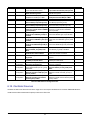
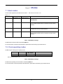
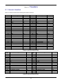
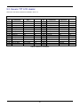
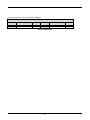
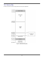
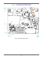
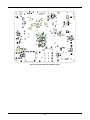
YRSPSH7267-0103 Renesas Starter Platform for SH7267 User's Manual RENESAS SINGLE-CHIP MICROCOMPUTER TM SuperH Rev.3.2 Revision date: May. 23, 2012 RISC engine Renesas Electronics America Inc www.renesas.com Disclaimer By using this Renesas Starter Platform (RSP), the user accepts the following terms. The RSP is not guaranteed to be error free, and the entire risk as to the results and performance of the RSP is assumed by the User. The RSP is provided by Renesas on an “as is” basis without warranty of any kind whether express or implied, including but not limited to the implied warranties of satisfactory quality, fitness for a particular purpose, title and non-infringement of intellectual property rights with regard to the RSP. Renesas expressly disclaims all such warranties. Renesas or its affiliates shall in no event be liable for any loss of profit, loss of data, loss of contract, loss of business, damage to reputation or goodwill, any economic loss, any reprogramming or recall costs (whether the foregoing losses are direct or indirect) nor shall Renesas or its affiliates be liable for any other direct or indirect special, incidental or consequential damages arising out of or in relation to the use of this RSP, even if Renesas or its affiliates have been advised of the possibility of such damages. Precautions This Renesas Starter Platform is only intended for use in a laboratory environment under ambient temperature and humidity conditions. A safe separation distance should be used between this and any sensitive equipment. Its use outside the laboratory, classroom, study area or similar such area invalidates conformity with the protection requirements of the Electromagnetic Compatibility Directive and could lead to prosecution. The product generates, uses, and can radiate radio frequency energy and may cause harmful interference to radio communications. However, there is no guarantee that interference will not occur in a particular installation. If this equipment causes harmful interference to radio or television reception, which can be determined by turning the equipment off or on, you are encouraged to try to corre ct the interference by one or more of the following measures; ensure attached cables do not lie across the equipment reorient the receiving antenna increase the distance between the equipment and the receiver connect the equipment into an outlet on a circuit different from that which the receiver is connected power down the equipment when not is use consult the dealer or an experienced radio/TV technician for help NOTE: It is recommended that wherever possible shielded interface cables are used. The product is potentially susceptible to certain EMC phenomena. To mitigate against them it is recommended that the following measures be undertaken; The user is advised that mobile phones should not be used within 10m of the product when in use. The user is advised to take ESD precautions when handling the equipment. The Renesas Starter Platform does not represent an ideal reference design for an end product and does not fulfil the regulatory standards for an end product. ii Table of Contents Chapter 1. Preface .................................................................................................................................................. 1 Chapter 2. Purpose ................................................................................................................................................. 2 Chapter 3. Power Supply ............................................................................................................................. ........... 3 3.1. Requirements ............................................................................................................................................... 3 3.2. Power–up Behaviour .................................................................................................................................... 3 Chapter 4. Board Layout ......................................................................................................................................... 4 4.1. Component Layout ....................................................................................................................................... 4 4.2. Board Dimensions ........................................................................................................................................ 5 Chapter 5. Block Diagram ............................................................................................................................. .......... 6 Chapter 6. User Circuitry............................................................................................................................ ............. 7 6.1. Switches ....................................................................................................................................................... 7 6.2. LEDs ............................................................................................................................................................. 7 6.3. Potentiometer ............................................................................................................................................... 7 6.4. Serial port ..................................................................................................................................................... 8 6.5. Debug LCD Module ...................................................................................................................................... 8 6.6. RCAN ........................................................................................................................................................... 9 6.7. USB .............................................................................................................................................................. 9 6.8. ETHERNET ................................................................................................................................................ 10 6.9. LCD Interface ............................................................................................................................................. 10 6.10. SSI ............................................................................................................................................................ 11 6.11. SD Card .................................................................................................................................................... 11 6.12. Video Decoder .......................................................................................................................................... 12 6.13. Option Links.............................................................................................................................................. 13 6.14. Oscillator Sources .................................................................................................................................... 15 6.15. Reset Circuit ............................................................................................................................................. 16 Chapter 7. Modes.................................................................................................................................................. 17 7.1. Boot modes ................................................................................................................................................ 17 7.2. Clock operating modes............................................................................................................................... 17 Chapter 8. Programming Methods ........................................................................................................................ 18 Chapter 9. Headers ............................................................................................................................................... 19 9.1. Generic Headers ........................................................................................................................................ 19 9.2. Generic TFT LCD Header .......................................................................................................................... 20 Chapter 10. Code Development ........................................................................................................................... 22 10.1. Overview................................................................................................................................................... 22 10.2. Compiler Restrictions ............................................................................................................................... 22 10.3. Breakpoint Support ................................................................................................................................... 22 10.4. Memory Map............................................................................................................................................. 23 Chapter 11. Component Placement ...................................................................................................................... 24 iii Chapter 12. Additional Information........................................................................................................................ 26 iv Chapter 1. Preface Cautions This document may be, wholly or partially, subject to change without notice. All rights reserved. Duplication of this document, either in whole or part is prohibited without the written permission of Renesas Electronics America. Trademarks All brand or product names used in this manual are trademarks or registered trademarks of their respective companies or organisations. Copyright © 2012 Renesas Electronics America. All rights reserved. Website: www.renesas.com Glossary ADC Analog to Digital Converter SCI Serial Communication Interface CD SD Secure Digital SDRAM Synchronous Compact Disc CPU Central Processing Unit DAC Digital to Analog Converter E10A ‘E10A for Starter Platforms’ Debugger EMC compatibility ESD Electrostatic Discharge High-Performance Embedded Workshop H-UDI Hitachi - User Debug Interface I/O Input / Output LCD Liquid Crystal Display LED Light Emitting Diode MCU Microcontroller Unit PC Personal Computer RAM Random Access Memory RCAN Renesas Controller Area Network ROM Read-Only Memory RSP Renesas Starter Platform plus Random Memory Electromagnetic HEW Dynamic 1 SPDIF Sony/Philips Digital Interface SSI Serial Sound Interface USB Universal Serial Bus Access Chapter 2. Purpose This RSP is an evaluation tool for Renesas microcontrollers. Features include: Renesas Microcontroller Programming. User Code Debugging. User Circuitry such as switches, LEDs and potentiometer(s). Sample Application. Sample peripheral device initialisation code. The RSP board contains all the circuitry required for microcontroller operation. This manual describes the technical details of the RSPSH7267 hardware. The Quick Start Guide and Tutorial Manual provide details of the software installation and debugging environment. 2 Chapter 3. Power Supply 3.1. Requirements This CPU board can operate from a 5V center positive power supply. Table 3-1 and Table 3-2 below details the power supply connectors available on this RSP board CN7 Pin CPU board Signal Name Pin CPU board Signal Name 1 5VCC 2 5VCC 3 GROUND 4 GROUND Table 3-1: Power Supply Connector CN7 Pin 1 3 CN8* CPU board Signal Name Pin 5VCC 2 GROUND CPU board Signal Name NC Note: The connector CN8 is underneath the board and is not normally installed. Table 3-2: Power Supply Connector CN8 Warning - Care must be taken to ensure that an appropriate supply is used. Failing to do this may cause permanent damage to the board. This RSP board is supplied with an E10A debugger. This RSP boards have a centre positive supply connector using a 2.0mm barrel power jack. Warning - The CPU board is not over voltage protected. Use a centre positive supply for this board. 3.2. Power–up Behavior When the RSP is purchased the CPU board has the ‘Release’ or stand alone code from the example tutorial code pre-programmed into the Renesas microcontroller. On powering up the board, the user LEDs will start to flash. Pressing any switch will cause the LEDs to flash at a rate controlled by the potentiometer. 3 Chapter 4. Board Layout 4.1. Component Layout The following diagram shows the top layer component layout of the board. Video Connector Power Connector Power LED’s Reset Switch Ethernet Jack TFT LCD Panel MCU Audio Jacks User LEDs E10A Header VGA Connector USB Host & Function(bottom) CAN RS232 Serial Connector User Switches Debug LCD Header Figure 4-1: Board Layout 4 4.2. Board Dimensions The following diagram gives the board dimensions and connector positions. Figure 4-2: Board Dimensions 5 Chapter 5. Block Diagram Figure 5-1 shows the CPU board components and their connectivity. Power Jack SD Card Connector QSPI 4MB LCD Panel Connector NAND Video Decoder NOR 4MB SH7267 Microcontroller TFT Header RCAN SDRAM 64MB Connector Ethernet Connector RESET IC Reset In ADC Inputs for User Switches USB Host & Function Connector Serial Sound Interface Connector Analog In Application Header User Switches Debug Headers Option 4 Serial Connectors Option LED’s User: 4 Yellow Potentiometer Figure 5-1: Block Diagram Figure 5-2 shows E10A connections to the RSP board. USB Cable Host PC E 10 A Module JP15 JP 8 J12 MCU User Interface Cable CN11 JP16 J6 USB CPU Board Figure 5-2: E10A RSP Connections 6 Power 3v3 5v Chapter 6. User Circuitry 6.1. Switches There are 16 user switches connected in matrix form on the board in addition to the reset switch. They are connected to 4 ADC input Pins of the MCU. The function of each switch and its connection are shown in Table 6-1 Switch RST / SW18 SW2 SW3 SW4 SW5 SW6 SW7 SW8 SW9 SW10 SW11 SW12 SW13 SW14 SW15 SW16 SW17 Function When pressed, the microcontroller is reset. User Switch User Switch User Switch User Switch User Switch User Switch User Switch User Switch User Switch User Switch User Switch User Switch User Switch User Switch User Switch User Switch Microcontroller RES#, Pin 46 PH0/AN0, Pin 80 PH0/AN0, Pin 80 PH0/AN0, Pin 80 PH0/AN0, Pin 80 PH1/AN1, Pin 81 PH1/AN1, Pin 81 PH1/AN1, Pin 81 PH1/AN1, Pin 81 PH2/AN2, Pin 82 PH2/AN2, Pin 82 PH2/AN2, Pin 82 PH2/AN2, Pin 82 PH3/AN3, Pin 83 PH3/AN3, Pin 83 PH3/AN3, Pin 83 PH3/AN3, Pin 83 Table 6-1: Switch Functions 6.2. LEDs There are 7 LEDs on the RSP board. The green ‘POWER’ LED (LED8) lit when a 3.3V supply is connected to the power net 3VCC and blue ‘POWER’ LED (LED7) lights when the board is powered with 5V. The four user LEDs are connected to an IO port and will lit when their corresponding port pin is set low. An Orange LED (D2) will light when Ethernet connection is established. Table 6-2 below shows the LED pin references and their corresponding microcontroller port pin connections. LED Reference (As shown on silkscreen) LED1 LED2 LED3 LED9 Colour Yellow Yellow Yellow Yellow Microcontroller Port Pin function PE4 PE5 PG20 PA_B0 Microcontroller Pin Number 134 133 58 48 (external buffered) Polarity Active Low Active Low Active Low Active Low Table 6-2: LED Port 6.3.Potentiometer A single-turn potentiometer is connected to pin AN4 of the microcontroller. This may be used to vary the input analog voltage value to this pin between AVCC and Ground. Note: The potentiometer is fitted to offer an easy way of supplying a variable analog input to the controller. It does not necessarily reflect the accuracy of the controller’s ADC. Please see the device manual for details. 7 6.4.Serial port The RS232 port is available at connector ‘CN1’ and uses microcontroller serial port SCIF0 for asynchronous serial communication. The board is designed to accept a straight-through RS-232 male-to-female cable. 6.5.Debug LCD Module The LCD module supplied with the RSP can be connected to the connector ‘J6’ for use with the tutorial code. Any module that conforms to the pin connections and has a KS0066u compatible controller can be used. The LCD module uses a 4bit interface to reduce the p in allocation. No contrast control is provided; this must be set on the display module. The module supplied with the CPU board only supports 5V operation. Table 6-3 shows the pin allocation and signal names used on this connector. Pin 1 3 5 7 9 11 13 Circuit Net Name Ground No Connection R/W (Wired to write only using 10K pull down)) No Connection No Connection PG20 PA_B1 J6 (For LCD) Device Pin Pin 2 4 6 58 49* 8 10 12 14 Circuit Net Name 5VCC PE4 PE5 (+ 10k pull down to ground) No Connection No Connection PA_B0 PA_B2 Table 6-3: Debug LCD Module Connections Note [*]: These pins are externally buffered. 8 Device Pin 134 133 48 * 62 * 6.6. RCAN The SH7267 on-chip RCAN module offers a flexible and sophisticated way to organize and control CAN frames, providing the compliance to CAN2.0B Active and ISO-11898-1. There are 2 CAN channels available on the microcontroller but only one transceiver is available on the board. By default CAN0 is connected to the CAN transceiver. Option links provide easy interface to connect CAN1 channel to the transceiver instead of CAN0. Table 6-4 details the required connections to connect either CAN0 or CAN1 channel to the transceiver – CAN channel Option Links Option Links R277, R278 R275, R276 CAN0 Fitted Removed CAN1 Removed Fitted Note: The default CAN setting on this RSP is indicated by BOLD text. Table 6-4: CAN Channel Selection Table 6-5 details the CAN connectors available on this RSP board – CAN0 Pin Circuit Net Name 1 CANH Device Pin 105 * (CTX1) 2 CANL 104* (CRX1) 3 GND - * - The RCAN transceivers translate the voltage levels on CPU pin to meet RCAN voltage level standards. Table 6-5: RCAN Connector For more details on SH7267 on-chip RCAN module, please refer to SH7267 Group Hardware Manual. 6.7. USB The USB 2.0 host/function module (USB) provides capabilities as a USB host and USB function. It supports high-speed and full-speed transfers defined by USB 2.0 specification. The Low speed mode is not supported. This module has a USB transceiver and supports all of the transfer types defined by the USB specification. The module has an 8-kbyte on-chip buffer memory for data transfer, providing a maximum of ten pipes. Any endpoint numbers can be assigned to PIPE1 to PIPE9, based on the peripheral devices or user system for communication. Table 6-6 below details the USB connectors available on this RSP board 9 Pin No 1 2 3 4 5 6 USB Socket-A (USB Host) JP1 (1-2) short Pin Name Circuit Net Device Pin Name VBUS VBUS 70 DDM 68 D+ DP 69 GND GROUND --FG2 USB_SHLD --FG1 USB_SHLD --- USB Mini-B (USB Device / Function) JP1 (1-2) open Pin No Pin Name Circuit Net Device Pin Name 1 VBUS VBUS 70 2 DDM 68 3 D+ DP 69 4 ID USB_ID NC 5 GND GROUND --6 FRAME USB_SHLD --7 FG1 USB_SHLD --8 FG2 USB_SHLD --9 FG3 USB_SHLD --Table 6-6: USB For more details on SH7267 on-chip USB module, please refer to SH7267 Group Hardware Manual. 6.8. ETHERNET The network functionality is provided by the SMSC LAN9218, a single-chip 10/100 Ethernet controller which incorporates essential protocol requirements for operating an Ethernet/IEEE 802.3 10BASE-T and 802.3u100BASE-TX node. The Ethernet controller is configured to use a 16 bit data bus. It uses single 16 bit read and write strobes. Byte accesses are not available for this device. The chip select used for the network controller is CS4. The orange LED (D2) lights when Full-Duplex connection is established between the PHY device and any other connected Ethernet devices. The embedded Ethernet connector green LED lights when there is a link with the other devices. The yellow LED lights when there is a network activity. Refer to the SMCS LAN9218 datasheet for more information on this peripheral. Table 6-7 contains details of the signal descriptions and pin connections. LED Reference (As shown on silkscreen) DUPLEX Ethernet connector: LED_K_YELLOW Ethernet connector: LED_K_GREEN Colour Orange Yellow Green LAN89218 Port Pin GPIO2_LED3# GPIO0_LED1# GPIO1_LED2# LAN9218 Pin Number 100 98 99 Table 6-7: Ethernet module settings 6.9. LCD Interface Video Display Controller 3 in SH7267 supports TFT-LCD panel. Video Display Controller 3 uses the display and recording function to store the input data in the memory and then display the video on the panel. NEC NL2432HC17-07B TFT LCD panel has been used on RSPSH7267 board. This panel has a resolution of 240 x 320 pixels. This panel is fitted at CN11 connector. Table 6-8 below details the pin connections for CN11 connector available on this RSP board Pin 1 3 5 7 CPU board Signal Name GROUND 3VCC 3VCC GROUND CN11 (For NEC LCD) Device Pin Pin CPU board Signal Name --2 GROUND --4 3VCC --6 3VCC --8 RES# 10 Device Pin ------46 9 11 13 15 17 19 21 23 25 27 29 31 33 35 37 39 41 43 45 PG17 LCD_CL1_HSYNC PG19 LCD_CLK GROUND PG1 LCD1_B2 PG3 LCD3_B4 PG5 LCD5_G0 PG7 LCD7_G2 PG9 LCD9_G4 GROUND PG12 LCD12_R2 PG14 LCD14_R4 GROUND PG23/MOSI1/TIOC0C PG22/SSL1/TIOC0B –NC XX+ GROUND VLED- 121 176 10 12 14 16 18 20 22 24 26 28 30 32 34 36 38 40 42 44 54 52 30 27 9 155 151 ---99 ---101 ----- LCD_FLM_VSYNC PG16 GROUND LCD0_B1 PG0 LCD2_B3 PG2 LCD4_B5 PG4 LCD6_G1 PG6 LCD8_G3 PG8 LCD10_G5 PG10 LCD11_R1 PG11 LCD13_R3 PG13 LCD15_R5 PG15 PG21/RSPCK1/TIOC0A PG24/MISO1/TIOC0D VCOM GROUND YY+ VLED+ 123 55 53 32 28 11 171 169 154 150 103 ---97 ----- Table 6-8: LCD Header CN11 6.10. SSI The serial sound interface (SSI) is a module designed to send or receive audio data interface with various devices offering Sony/Philips Digital Interconnect Format (S/PDIF) compatibility. It also provides additional modes for other common formats, as well as support for multi-channel mode. Both transmitter and receiver modules are embedded. Audio Codec pins are available at header ‘CN10’. 6.11. SD Card SD card memory interface is provided in this controller. Note: The SD card memory interface is not available in the RSP SH7267 default setting. To use the SD card memory interface, fit the following optional resistors: R286, R287, R288, R289, R290, R291, R26, R305, and R304; and remove the default resistors: R133, R134, R135, R136, R301, and R302. Table 6-9 below details the SD Card header. J1 Pin Header Name Circuit Net Name Device Pin 1 CD/DAT3 SD_D3 117 3 VSS1 GROUND 5 CLK 7 Pin Header Name Circuit Net Name Device Pin 2 CMD SD_CMD 116 --- 4 VDD 3VCC_C --- SD_CLK 115 6 VSS2 GROUND --- DAT0 SD_D0 113 8 DAT1 SD_D1 111 9 DAT2 SD_D2 118 10 W_Protect SD_WP 109 11 Card_Detect SD_CD 108 12 COMMON GROUND --- Table 6-9: SD Card Header 11 6.12.Video Decoder The video display controller provides video display function, video recording function, utility for overlaying graphics images on the input video, and function for outputting the control signals for the TFT-LCD panel. Note: The video display controller is not available in the RSP SH7267 default setting. To use the video display controller, fit the following optional resistors: R69, R70, R71, R72, R73, R74, R75, R76, R80, R82, and R83; and remove the default resistors: R133, R134, R135, R136, R301, and R302. Table 6-10 below details the Video Decoder header pin connections CN10 Pin Circuit Net Name Device Pin Pin Circuit Net Name Device Pin 1 PE5/DV_HSYNC/SDA2 133 2 RES# 46 3 PE4/DV_VSYNC/SCL2 134 4 PE3/SDA1 135 5 PF0/DV_DATA0 119 6 PE2/SCL1 136 7 GROUND --- 8 3VCC --- 9 PF8/DV_CLK 108 10 PF4/DV_DATA4 115 11 PF1/DV_DATA1 118 12 PF5/DV_DATA5 113 13 PF2/DV_DATA2 117 14 PF6/DV_DATA6 111 15 PF3/DV_DATA3 116 16 PF7/DV_DATA7 109 Table 6-10: Video Decoder Header CN10 Table 6-11 below details the VGA connector pin connections J9 Header Pin 1 3 5 7 9 11 13 15 RSP board Signal Name Header Pin crt_red crt_blue GROUND GROUND NC NC LCD_CL1_HSYNC* NC 2 4 6 8 10 12 14 Table 6-11: VGA Connector * - These CPU pins are connected through a NAND gate 12 RSP board Signal Name crt_green NC GROUND GROUND GROUND NC LCD_FLM_VSYNC* 6.13. Option Links In this section, the default configuration is indicated by BOLD text. Table 6-12 describes the function of the option links associated with LCD configuration. LCD interface Settings R209 LCD Interface Connects Clock pin 26 of DAC to Disconnects Clock pin 26 of DAC from GROUND GROUND R210 LCD Interface Connects signal R0 of Video DAC to Disconnects signal R0 of Video DAC from ground ground R212 LCD Interface Connects signal R1 of Video DAC to Disconnects signal R1 of Video DAC from ground ground R213 LCD Interface Connects signal R2 of Video DAC to Disconnects signal R2 of Video DAC from ground ground R211 LCD Interface Connects signal R3 of Video DAC to Disconnects signal R3 of Video DAC from PG11 (pin 169) of MCU PG11 (pin169) of MCU R214 LCD Interface Connects signal R4 of Video DAC to Disconnects signal R4 of Video DAC from PG12 (pin 155) of MCU PG12 (pin155) of MCU R215 LCD Interface Connects signal R5 of Video DAC to Disconnects signal R5 of Video DAC from PG13 (pin 154) of MCU PG13 (pin154) of MCU R216 LCD Interface Connects signal R6 of Video DAC to Disconnects signal R6 of Video DAC from PG14 (pin 151) of MCU PG14 (pin151) of MCU R217 LCD Interface Connects signal R7 of Video DAC to Disconnects signal R7 of Video DAC from PG15 (pin 150) of MCU PG15 (pin150) of MCU R218 LCD Interface Connects signal G0 of Video DAC to Disconnects signal G0 of Video DAC from ground ground R219 LCD Interface Connects signal G1 of Video DAC to Disconnects signal G1 of Video DAC from ground ground R220 LCD Interface Connects signal G2 of Video DAC to Disconnects signal G2 of Video DAC from PG5 (pin30) of MCU PG5 (pin30) of MCU R221 LCD Interface Connects signal G3 of Video DAC to Disconnects signal G3 of Video DAC from PG6 (pin28) of MCU PG6 (pin28) of MCU R222 LCD Interface Connects signal G4 of Video DAC to Disconnects signal G4 of Video DAC from PG7 (pin27) of MCU PG7 (pin27) of MCU R224 LCD Interface Connects signal G5 of Video DAC to Disconnects signal G5 of Video DAC from PG8 (pin11) of MCU PG8 (pin11) of MCU R225 LCD Interface Connects signal G6 of Video DAC to Disconnects signal G6 of Video DAC from PG9 (pin 9) of MCU PG9 (pin9) of MCU R226 LCD Interface Connects signal G7 of Video DAC to Disconnects signal G7 of Video DAC from PG10 (pin 171) of MCU PG10 (pin171) of MCU R227 LCD Interface Connects signal B0 of Video DAC to Disconnects signal B0 of Video DAC from ground ground R228 LCD Interface Connects signal B1 of Video DAC to Disconnects signal B1 of Video DAC from ground ground R229 LCD Interface Connects signal B2 of Video DAC to Disconnects signal B2 of Video DAC from ground ground R230 LCD Interface Connects signal B3 of Video DAC to Disconnects signal B3 of Video DAC from PG0 (pin55) of MCU PG0 (pin55) of MCU R231 LCD Interface Connects signal B4 of Video DAC to Disconnects signal B4 of Video DAC from PG1 (pin54) of MCU PG1 (pin54) of MCU R232 LCD Interface Connects signal B5 of Video DAC to Disconnects signal B5 of Video DAC from PG2 (pin53) of MCU PG2 (pin53) of MCU R233 LCD Interface Connects signal B6 of Video DAC to Disconnects signal B6 of Video DAC from PG3 (pin52) of MCU PG3 (pin52) of MCU R238 LCD Interface Connects the BLANK pin of Video Disconnects the BLANK pin of Video DAC DAC to PG18 (pin2) of MCU from PG18 (pin2) of MCU R234 LCD Interface Connects signal B7 of Video DAC to Disconnects signal B7 of Video DAC from PG4 (pin32) of MCU PG4 (pin32) of MCU 13 ----------------------------------------------------- R268 LCD Interface Connects PJ2 pin of MCU to LCD_M_DISP pin of TFT LCD connector (JP12) Disconnects PJ2 pin of MCU from LCD_M_DISP pin of TFT LCD connector (JP12) R269, R275 Table 6-12: LCD Configuration links Table 6-13 describes the function of miscellaneous option links. Option Link Settings Reference Function Fitted Alternative (Removed) R266 Touch Screen Connects ADGTRG pin to 3VCC Disconnects ADGTRG pin from 3VCC Configuration R267 Touch Screen Connects IRQ0 pin of the MCU to 3VCC Disconnects IRQ0 pin of the MCU from Configuration 3VCC R275 CAN Configuration R276 CAN Configuration CAN Configuration CAN Configuration R277 R278 R53 R54 R281 R282 R65 Serial Flash Interface Serial Flash Interface Serial Flash Interface Serial Flash Interface R86 R90 SDRAM Interface NAND Flash Interface NOR Flash interface NOR Flash interface NOR Flash interface NOR Flash interface Video Decoder Video Decoder R1 R252 R251 R250 R253 Power Supply Power Supply Power Supply Power Supply Oscillator R248 R249 R57 USB USB USB R32 R33 R34 R35 R36 Connects PJ2 pin of MCU to CTX1 pin of voltage translator circuit in CAN module. Connects IRQ1 pin of MCU to CXR1 pin of voltage translator in CAN module. Connects the CTX0 of MCU pin to pin 1 of HA13721 (CAN Intf.) Connects the CRX0 of MCU pin to pin 3 of voltage translator in CAN circuit Connects RESET pin of Serial Flash to 3VCC Connects RESET pin of Serial Flash to the CPU reset pin Connects the D pin of Serial Flash to pin 3 of J10 connector Connects the Q pin of Serial Flash to pin 2 of J10 connector and MCU port pin PF2 Pull down resistor for CKE pin of the MCU Connects the WP pin of NAND flash memory to 3VCC Connects an external address line A25 of MCU to pin 56 of NOR Flash memory Connects an external address line A24 of MCU to pin 1 of NOR Flash memory Connects an external address line A23 of MCU to pin 2 of NOR Flash memory Connects an external address line A22 to pin 15 of NOR Flash memory Pull up resistor for the MCU pin CLKINV Connects CLKINV pin of Video Decoder to ground Connects 1.2VCC to PLL1.2V Connects 1.2VCC to UA1.2V Connects 3VCC_CPU to UA3V Connects 3VCC_CPU to AVcc Connects X9 Crystal to EXTAL pin 57 of MCU Parallel resistor for inductor L1 Parallel resistor for inductor L3 Connects 5V supply to the Supply pin of power distribution switch MIC2025 (U7) 14 Related To R267, R236 R266, R236 Disconnects PJ2 pin of MCU from CTX1 pin of voltage translator. R268,R269 , R276 Disconnects IRQ1 pin of MCU from CXR1 pin of voltage translator in CAN module. Disconnects the CTX0 of MCU pin from pin 1 of HA13721 (CAN Intf.) Disconnects the CRX0 of MCU pin from pin 3 of voltage translator in CAN circuit R275 Disconnects RESET pin of Serial Flash from 3VCC Disconnects RESET pin of Serial Flash from CPU reset pin Disconnects the D pin of Serial Flash from pin 3 of J10 connector Disconnects the Q pin of Serial Flash from pin 2 of J10 connector and MCU port pin PF2 R54 Disconnects CKE pin of MCU from the Pull down resistor Disconnects the WP pin of NAND flash memory from 3VCC Disconnects the address line A25 of MCU from pin 56 of Nor Flash memory Disconnects the address line A24 from pin 1 of Nor Flash memory Disconnects the address line A23 from pin 2 of Nor Flash memory Disconnects the address line A22 from pin 15 of NOR Flash memory Disconnects the pull up from CLKINV pin Disconnects CLKINV pin of Video Decoder from ground Disconnects 1.2VCC from PLL1.2V Disconnects 1.2VCC from UA1.2V Disconnects 3VCC_CPU from UA3V Disconnects 3VCC_CPU from AVcc Disconnects crystal ‘X9’ from EXTAL pin 57 of MCU Parallel resistor removed Parallel resistor removed Disconnects 5V supply from the supply pin of U7 --- ----- R53 ----- --R37 R38 R39 R40 R90 R86 --------------- R68 Video Decoder R78 Video Decoder R91 User Port R140 Audio Interface R141 Audio Interface R133 Audio Interface R134 Audio Interface R135 Audio Interface R136 Audio Interface R143 Audio Interface R139 Audio Interface R137 MIC R146 Headphone R293 Ethernet Configuration Ethernet Configuration R283 R284 Ethernet Configuration R265 Ethernet Configuration Connects IIC bus address select (pin 73) of Video decoder to 3VCC Connects IIC bus control pin 73 of Video decoder to ground Connects the control input pin 1 of multiplexer to the RES pin of MCU Disconnects IIC bus address select (pin 73) of Video decoder from pull up circuit. Disconnects IIC bus control pin 73 of Video decoder from ground Disconnects the control input pin 1 of multiplexer from the RES pin of MCU R78 Connects Data input pin 17 of Audio driver to MCU port pin PE3 (pin135) Connects clock input pin 16 of Audio driver to MCU port pin PE2 (pin136) Connects ADC and DAC sample rate clock pin 7 of audio driver to SSIWS1 (pin115) of MCU Connects digital audio clock pin 8 of audio driver to SSISCK1 (pin116) of the MCU Connects ADC Data output (pin 9) of audio driver to SSIDATA1 (pin113) of the MCU Connects DAC data input pin 10 of audio driver toSSIDATA2 (pin108) of the MCU Connects chip select pin of audio driver to AUDIO_X1 (pin96) of the MCU Connects the analog output pin 21 of audio driver to TP11 on board Connects the pin 1 of CN2 connector to ground Connects the pin 4 of CN4 connector to GPIO2 pin of audio driver Connects PB22 (pin 43) of MCU to Chip select pin of Ethernet Connects pin FIFO_SEL of LAN89218 to the external address pin A11 (pin22) of the MCU Connects the interrupt request pin of Ethernet controller to IRQ1 pin (port pin 137) of MCU Connects ‘endianess select’ pin of Ethernet controller to the address pin A19 (pin37) of MCU Disconnects Data input pin 17 of Audio driver from MCU port pin PE3 (pin135) Disconnects clock input pin 16 of Audio driver from MCU port pin PE2 (pin 136) Disconnects ADC and DAC sample rate clock pin 7 of audio driver from SSIWS1 (pin115) of MCU Disconnects digital audio clock pin 8 of audio driver from SSISCK1 (pin 116) of the MCU --- Disconnects ADC Data output (pin 9) of audio driver from SSIDATA1 (pin113) of the MCU Disconnects DAC data input (pin 10) of audio driver from SSIDATA2 (pin 108) of the MCU --- Disconnects chip select pin of audio driver from AUDIO_X1 (pin96) of the MCU --- Disconnects the analog output pin 21 of audio driver fromTP11 on board Disconnects the pin 1 of CN2 connector from ground Disconnects the pin 4 of CN4 connector from GPIO2 pin of audio driver Disconnects PB22 (pin 43) of MCU from chip select pin of Ethernet Disconnects pin FIFO_SEL of LAN89218 from the address pin A11 (pin22) of the MCU Disconnects the interrupt request pin of Ethernet controller from IRQ1 (pin137) of MCU Disconnects ‘endianess select’ pin of Ethernet controller from the address pin A19 (pin37) of MCU --- R68 R280, R92 ------- --- ----R268, R275 R179 ----- Table 6-13: Miscellaneous Configuration links 6.14. Oscillator Sources Oscillators are fitted on the CPU board and used to supply various clock inputs to the Renesas microcontroller. Table 6-14 details the oscillators that are fitted and alternative footprints provided on this CPU board: 15 Oscillator (X1) Not Fitted Oscillator (X2) Not Fitted Crystal (X4) Fitted Oscillator (X5) Not Fitted Crystal (X6) Component 25.175MHz LCD Clock - For Test Purposes 32.768KHz Real Time Clock - For Test Purposes Fitted 48 MHz USB Clock Oscillator (X7) Fitted 24.576MHz Video Decoder Clock Crystal (X9) Fitted 12MHz System Clock Oscillator (OSC1) Fitted 13Mhz External DAC/ADC Clock Crystal (Y1) Fitted 25MHz Ethernet Clock Table 6-14: Oscillators / Resonators 6.15. Reset Circuit The CPU Board includes a Reset IC DS1819C (Q9) to meet the minimum reset period of 200 msec. The DS1819 monitor three vital conditions for a microprocessor: power supply, software execution, and external override. Please refer to the hardware manual for more information on the requirements of the reset circuit. Please check the reset requirements carefully to ensure the reset circuit on the user’s board meets all the reset timing requirements. 16 Chapter 7. Modes 7.1. Boot modes The boot modes supported by this RSP board are listed in. Table 7-1 Boot Mode Note: Please ensure that SW1-6 is ON 0 SW1-2 (MD_BOOT1 pin) ON SW1-3 (MD_BOOT0 pin) ON Description 1 ON OFF Boots the MCU, through high-speed communication, from the 4MB serial flash memory (connected to channel 0 of SPI interface) 2 OFF ON Boots the MCU from the 512 MB NAND flash memory (connected to the NAND flash memory controller interface) 3 OFF OFF Boots the MCU, through low-speed communication, from the 4MB serial flash memory (connected to channel 0 of SPI interface) Boots the MCU, from the 4MB NOR flash memory (connected to the CS0 space) Note: Please ensure that SW1-6 is ON Table 7-1: Boot Mode pin settings The default boot mode of this RSP is indicated by BOLD text. For more information on the boot modes listed above, please refer to the SH7267 group hardware manual. 7.2. Clock operating modes This RSP supports following clock operating modes Mode 0 1 SW1-1 (MD_CLK pin) ON OFF Clock Source EXTAL or crystal resonator USB_X1 or crystal resonator Note: Please ensure that SW1-6 is ON Table 7-2: Boot Mode pin settings The default clock operating mode of this RSP is indicated by BOLD text. For more information on the clock operating modes listed above, please refer to the SH7267 group hardware manual. 17 Chapter 8. Programming Methods The board is intended for use with HEW and the supplied E10A debugger. Refer to SH7267 Group Hardware Manual for details of programming/ debugging without using these tools. 18 Chapter 9. Headers 9.1. Generic Headers Table 9-1 to Table 9-2 below show the standard generic header connections. Header Pin 1 3 5 7 9 11 13 15 17 19 21 23 25 27 29 31 33 35 37 39 41 43 45 47 49 51 53 55 CPU board Signal Name 5VCC A22 A21 A20 A19 A18 A17 A16 A15 GROUND A14 A13 A12 A11 A10 A9 A8 A7 GROUND A6 A5 A4 A3 A2 A1 NC NC NC Device pin --43 39 38 37 36 35 34 26 --25 24 23 22 20 18 16 15 --14 13 8 7 6 4 Header Pin 2 4 6 8 10 12 14 16 18 20 22 24 26 28 30 32 34 36 38 40 42 44 46 48 50 52 54 56 CPU board Signal Name 3VCC PD15 PD14 PD13 PD12 PD11 PD10 PD9 PD8 GROUND PD7 PD6 PD5 PD4 PD3 PD2 PD1 PD0 GROUND PC0/CS0# PC1/RD# PC2/RD/WR# PC3/WE0#/DQML PC4/WE1#/DQMU PC5B/RAS# PC6B/CAS# PC7B/CKE PC8B/CS3# Device pin --131 132 139 140 142 144 145 146 --147 148 149 156 157 158 159 160 --161 163 165 166 167 168 173 174 175 Table 9-1: JP15 microcontroller header Header Pin 1 3 5 7 9 11 13 15 17 19 21 23 25 27 29 31 CPU board Signal Name 5VCC NC NC GROUND NC NC NC NC NC NC NC NC GROUND PG21/RSPCK1/TIOC0A PG22/SSL1/TIOC0B PG23/MOSI1/TIOC0C Device pin ----- --103 101 99 Header Pin 2 4 6 8 10 12 14 16 18 20 22 24 26 28 30 32 CPU board Signal Name 3VCC PH0/AN0 PH1/AN1 PH2/AN2 PH3/AN3 GROUND TP_AN4 TP_AN5 NMI GROUND NC PJ0/CTX0/IETXD PJ1/CRX0/IERXD PG24/MISO1/TIOC0D NC GROUND Table 9-2: JP16 microcontroller header 19 Device pin --80 81 82 83 --85 87 44 --107 106 ---97 ----- 9.2. Generic TFT LCD Header Generic TFT LCD header connections are detailed in Table 9-3. JP12 Header Pin 1 3 5 7 9 11 13 15 17 19 21 23 25 27 29 Generic TFT LCD Header Name ----LCD14_R4 LCD12_R2 LCD10_G5 LCD8_G3 LCD6_G1 LCD4_B5 LCD2_B3 LCD0_B1 VLCD_CLK --LCD_FLM_VSYNC LCD_M_DISP --- RSP board Signal Name 3VCC 3VCC PG14 PG12 PG10 PG8 PG6 PG4 PG2 PG0 NC NC PG16 LCD_M_DISP GROUND Device Pin ----151 155 171 11 28 32 53 55 ----123 105 --- Header Pin 2 4 6 8 10 12 14 16 18 20 22 24 26 28 30 Generic TFT LCD Header Name --LCD15_R5 LCD13_R3 LCD11_R1 LCD9_G4 LCD7_G2 LCD5_G0 LCD3_B4 LCD1_B2 --LCD_CL1_HSYNC --LCD_DISP ----- Table 9-3: Generic TFT LCD Header 20 RSP board Signal Name 3VCC PG15 PG13 PG11 PG9 PG7 PG5 PG3 PG1 GROUND PG17 NC PG18 GROUND GROUND Device Pin --150 154 169 9 27 30 52 54 --121 --2 ----- Generic SPDIF header connections are detailed in Table 9-4. J10 Header Pin 1 3 RSP board Signal Name Device Pin 3VCC SPDIF_IN --125 Header Pin 2 4 RSP board Signal Name Device Pin SPDIF_OUT GROUND 124 --- Table 9-4: SPDIF Header 21 Chapter 10. Code Development 10.1. Overview Note: For all code debugging using Renesas software tools, the CPU board must be connected to a PC USB port via an E10A. An E10A is supplied with the RSP product. An E10A supplied with this Platform is an on-chip debugging emulator which supports the H-UDI interface of the target device. The H-UDI uses a 14-pin interface and marked as E10A on the RSPSH7267 board. Due to the continuous process of improvements undertaken by Renesas the user is recommended to review the information provided on the Renesas website at www.renesas.com to check for the latest updates to the Compiler and Debugger manuals. 10.2. Compiler Restrictions The compiler supplied with this RSP is fully functional for a period of 60 days from first use. After the first 60 days of use have expired, the compiler will default to a maximum of 256k code and data. To use the compiler with programs greater than this size you will need to purchase the full version tools from your Renesas distributor Warning: The protection software for the compiler will detect changes to the system clock. Changes to the system clock back in time may cause the trial period to expire prematurely. 10.3. Breakpoint Support Limited Event Conditions can be located in ROM code which is directly supported by E10A emulator. To enable breakpoints in RAM following command needs to be included in the script – > SH2A_SBSTK enable For more information on this, please refer to the SuperH™ Family E10A-USB Emulator Additional Document for User’s Manual for SH7267. 22 10.4. Memory Map The memory map shown in this section visually describes the memory areas of RSPSH7267. Figure 10-1: RSPSH7267 Memory Map 23 Chapter 11. Component Placement Figure 11-1: Component Placement (Top Layer) 24 Figure 11-2: Component Placement (Bottom Layer) 25 Chapter 12. Additional Information For details on how to use High-performance Embedded Workshop (HEW), refer to the HEW manual available on the CD or installed in the Manual Navigator. For information about the SH7267 microcontrollers refer to the SH7267 Group Hardware Manual For information about the SH7267 assembly language, refer to the SH2A, SH2A-FPU Software Manual For information about the E10A Emulator, please refer to the E10A-USB Emulator User’s Manual Online technical support and information is available at: www.renesas.com/renesas_starter_Platforms Technical Contact Details America: [email protected] Europe: [email protected] Japan: [email protected] General information on Renesas Microcontrollers can be found on the Renesas website at: 26 www.renesas.com Renesas Starter Platform for SH7267 User's Manual Publication Date Rev.1.00 Published by: Renesas Electronics America Inc ©2012 Renesas Electronics America, All Rights Reserved. Renesas Starter Platform Plus for SH7267 User's Manual Renesas Electronics America Inc