1
TI Designs
IO-Link PHY BoosterPack
TI Designs
Design Features
TI Designs provide the foundation that you need
including methodology, testing, and design files to
quickly evaluate and customize the system. TI Designs
help you accelerate your time to market.
•
Design Resources
TIDA-00339
SN65HVD102
TPS7A1633
Design Folder
•
•
IO-Link V1.1 and V1.0 Connectivity Out-of-the-Box
(TMG Stack, Physical Interface Device (PHY), and
M12 Connector)
Simple Interfacing of Sensors
Designed to Meet With: IEC 61000-4-2, IEC 610004-4, IEC 61000-4-5, and IEC 60255-5 Standards
Featured Applications
Product Folder
Product Folder
MSP-EXP430FR4133
Tool Folder
TI LaunchPad Ecosystem Tool Folder
ASK Our E2E Experts
WEBENCH® Calculator Tools
•
•
•
•
•
Sensors and Field Transmitters
Factory Automation and Process Control
Field Actuators
Building Automation
Portable Instrumentation
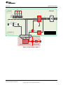
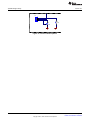
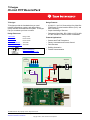
VCC
TIDA-00339
IO-Link PHY
Status Information
On J5 and LEDs
J5
SN65HVD102
Protection
PWR
CURR
TEMP
WAKE
STATUS
UART
VCC
L+
C/Q
L-
J3
J9
VCC in
J11
VCC
UART TX
UART RX
ENBL
GND
I_lim
SPI CLK
SPI MISO
SPI MOSI
SPI CS1
J1
3V3 MCU
J2
3V3 LDO
TPS7A1633
SPI/I2C for interfacing
Sensor on J11
Monitoring UART on J11
TIDA-00339 powered by
J1
J2
3V3 from Launchpad
X
-
3V3 from LDO
-
X
3V3 from LDO + powering Launchpad
X
X
Launchpad / BoosterPack
Connector
All trademarks are the property of their respective owners.
TIDU681A – January 2015 – Revised January 2015
Submit Documentation Feedback
Copyright © 2015, Texas Instruments Incorporated
IO-Link PHY BoosterPack
1
Key System Specifications
www.ti.com
An IMPORTANT NOTICE at the end of this TI reference design addresses authorized use, intellectual property matters and other
important disclaimers and information.
1
Key System Specifications
PARAMETER
SPECIFICATION
IO-Link Version
V1.1 (Compatible to V1.0)
SIO Mode
Supports SIO Mode
IO-Link
BAUD Rate Support
Designed to Standards
2
COM1, COM2, and COM3
IEC 61000-4-2, IEC 61000-4-4, IEC 61000-4-5, and IEC 60255-5
Modular Design
Easy to use with existing LaunchPads
Sensor Front-End
SPI or I2C Interface for sensor via BoosterPack or external
IO-Link PHY
Easy access to all signals of IO-Link PHY (SN65HVD102)
IO-Link PHY BoosterPack
TIDU681A – January 2015 – Revised January 2015
Submit Documentation Feedback
Copyright © 2015, Texas Instruments Incorporated
System Description
www.ti.com
2
System Description
The TI design TIDA-00339 is a fully IO-Link compliant design enabling the user to easily evaluate the IOLink communication. The modular approach is capable of use with different MCUs (microcontrollers)
based on the LaunchPad and BoosterPack ecosystem and also allows the user to test his or her own
sensor front-end.
2.1
IO-Link Interface
The system incorporates an IO-Link PHY plus protection circuit (bypassable) and a standard M12, 4-pin,
A-coded connector, which can be connected to any IO-Link master system and supports IO-Link V1.1 and
V1.0.
The design also allows use of the IO-Link PHY in SIO Mode, either manually (through the switch button)
or through MCU communication.
2.2
Power Supply
A high input voltage, low-dropout regulator (LDO) (VIN_max = 60 V) can generate 3.3-V VCC of the system
directly from the nominal 24 V of the IO-Link L+ line, while withstanding potential high voltage inputs
during surge conditions. Alternatively, the connected LaunchPad can power the system.
2.3
TI LaunchPad and BoosterPack Ecosystem
TIDA-00339 must be used in combination with an MCU, on which the IO-Link stack is running. The
advantage of the design in the BoosterPack pin-out is the flexible option of using an MCU that best suits
the needs of the customer. Many TI MCUs are available as a LaunchPad, which can easily connect to the
IO-Link PHY BoosterPack design.
This design guide uses the LaunchPad MSP-EXP430FR4133 to showcase features.
View further information on TI's LaunchPad and BoosterPack ecosystem here: www.ti.com/launchpad.
2.4
Sensor Front-End
In addition to the actual IO-Link PHY evaluation, the system allows users to attach their own sensor frontends with a serial peripheral interface (SPI) or I2C interface. Two options are available for the user:
1. Sensor attach through headers: the TI design provides easy access to the MCUs SPI and I2C interface
on the board. An external sensor front-end with an SPI or I2C interface can be connected.
2. Sensor attach through BoosterPack: the LaunchPad ecosystem allows the connection of several
BoosterPacks. This design also allows an additional BoosterPack (containing a sensor front-end) to
stack up and communicate with the MSP430™ of the LaunchPad. For example,
the TIDA-00168 Thermocouple AFE has been developed to also be used as a BoosterPack.
TIDU681A – January 2015 – Revised January 2015
Submit Documentation Feedback
Copyright © 2015, Texas Instruments Incorporated
IO-Link PHY BoosterPack
3
Block Diagram
3
www.ti.com
Block Diagram
VCC
TIDA-00339
IO-Link PHY
Status Information
On J5 and LEDs
J5
SN65HVD102
Protection
PWR
CURR
TEMP
WAKE
STATUS
UART
VCC
L+
C/Q
L-
J3
J9
VCC in
J11
VCC
UART TX
UART RX
ENBL
GND
I_lim
SPI CLK
SPI MISO
SPI MOSI
SPI CS1
J1
3V3 MCU
J2
3V3 LDO
TPS7A1633
SPI/I2C for interfacing
Sensor on J11
Monitoring UART on J11
TIDA-00339 powered by
J1
J2
3V3 from Launchpad
X
-
3V3 from LDO
-
X
3V3 from LDO + powering Launchpad
X
X
Launchpad / BoosterPack
Connector
Launchpad
MSP430
IO-Link Stack
On MCU of
Launchpad
Launchpad / BoosterPack
Connector
Booster Pack
Additional Booster Packs can be connected
Figure 1. TIDA-00339 System Block Diagram
3.1
3.1.1
Highlighted Products
SN65HVD102
The SN65HVD101 and SN65HVD102 IO-Link PHYs implement the IO-Link interface for industrial point-topoint communication. When the device is connected to an IO-Link master through a 3-wire interface, the
master can initiate communication and exchange data with the remote node, while the SN65HVD10X acts
as a complete physical layer for the communication.
The IO-Link driver output (CQ) can be used in push-pull, high-side, or low-side configurations using the
EN and TX input pins. The PHY receiver converts the 24-V IO-Link signal on the CQ pin to standard logic
levels on the RX pin. The use of a simple parallel interface transmits and receives data and status
information between the PHY and the local controller.
The SN65HVD101 and SN65HVD102 implement protection features for overcurrent, overvoltage, and
overtemperature conditions. The IO-Link driver current limit can be set using an external resistor. If a
short-circuit current fault occurs, the driver outputs are internally limited and the PHY generates an error
signal (SC). These devices also implement an overtemperature shutdown feature that protects the device
from high-temperature faults.
4
IO-Link PHY BoosterPack
TIDU681A – January 2015 – Revised January 2015
Submit Documentation Feedback
Copyright © 2015, Texas Instruments Incorporated
Block Diagram
www.ti.com
The SN65HVD102 operates from a single external 3.3-V or 5-V local supply. The SN65HVD101 integrates
a linear regulator that generates either 3.3 V or 5 V from the IO-Link L+ voltage for supplying power to the
PHY, as well as a local controller and additional circuits.
The SN65HVD101 and SN65HVD102 are available in the 20-pin RGB package (4 mm × 3.5 mm quad flat
no leads (QFN)) for space-constrained applications.
VCC
OUT
VCC VCC
IN SET
L+
SUPPLY VOLTAGE
CONTROL
PWR_OK
RX
CQ
TX
Voltage
Timers
EN
Control
Logic
WAKE
Voltage
Detectors
L-
Over Current Over Current
Timers
Detectors
TEMPERATURE
SENSE
CUR_OK
TEMP_OK
ILIM_ADJ
GND
L-
Figure 2. Functional Block Diagram SN65HVD102
•
•
•
•
•
•
•
•
•
•
•
3.1.2
Configurable CQ output: push-pull, high-side, or low-side for SIO Mode
Remote wake-up indicator
Current limit indicator
Power-good indicator
Overtemperature protection
Reverse polarity protection
Configurable current limits
9-V to 36-V supply range
Tolerant to 50-V peak line voltage
3.3-V or 5-V configurable integrated LDO (SN65HVD101 only)
20-pin QFN package, 4 mm × 3.5 mm
TPS7A1633
The TPS7A16 family of ultra-low power, LDO voltage regulators offers the benefits of ultra-low quiescent
current, high input voltage, and miniaturized, high thermal-performance packaging.
The TPS7A16 family is designed for continuous or sporadic (power backup) battery-powered applications
where ultra-low quiescent current is critical to extending the system battery life.
The TPS7A16 family offers an enable pin (EN) compatible with standard complementary metal-oxidesemiconductor (CMOS) logic and an integrated, open-drain, and active-high power good output (PG) with
a user-programmable delay. These pins are intended for use in microcontroller-based, battery-powered
applications where power-rail sequencing is required.
In addition, the TPS7A16 is ideal for generating a low-voltage supply from multi-cell solutions ranging from
high cell-count power-tool packs to automotive applications. Not only can this device supply a wellregulated voltage rail, but it can also withstand and maintain regulation during voltage transients. These
features translate to simpler and more cost-effective, electrical surge-protection circuitry.
TIDU681A – January 2015 – Revised January 2015
Submit Documentation Feedback
Copyright © 2015, Texas Instruments Incorporated
IO-Link PHY BoosterPack
5
Block Diagram
www.ti.com
Figure 3. Functional Block Diagram TPS7A1633
•
•
•
•
•
•
•
•
•
•
•
•
3.1.3
Wide input voltage range: 3 V to 60 V
Ultra-low quiescent current: 5 µA
Quiescent current at shutdown: 1 µA
Output current: 100 mA
Low dropout voltage: 60 mV at 20 mA
Accuracy: 2%
Available in:
– Fixed output voltage: 3.3 V, 5.0 V
– Adjustable version from approximately 1.2 V to 18.5 V
Power good with programable delay
Current-limit and thermal shutdown protections
Stable with ceramic output capacitors: ≥ 2.2 µF
Package: high thermal performance MSOP-8 PowerPAD™
Operating temperature range: –40°C to 125°C
MSP-EXP430FR4133
The MSP-EXP430FR4133 LaunchPad development kit is an easy-to-use evaluation module (EVM) for the
MSP430FR4133 microcontroller. The development kit contains everything needed to start developing on
the MSP430 ultra-low power (ULP) FRAM-based microcontroller platform, including on-board emulation
for programming, debugging, and energy measurements. The board features on-board buttons and LEDs
for the quick integration of a simple user interface as well as a liquid crystal display (LCD), which
showcases the integrated driver with flexible software-configurable pins. The MSP430FR4133 device
features embedded FRAM (ferroelectric random access memory), a non-volatile memory known for its
ultra-low power, high endurance, and high-speed write access.
Rapid prototyping is simplified by the 20-pin BoosterPack plug-in module headers, which support a wide
range of available BoosterPacks. Users can quickly add features like wireless connectivity, graphical
displays, environmental sensing, and much more. Users can also design a customized BoosterPack or
choose among many already available from TI and third-party developers.
The out-of-box functionality provided with the MSP-EXP430FR4133 LaunchPad features the on-board
segmented display and offers two operating modes. Stop-Watch Mode can run a timer for up to 100
hours, or alternatively operate split time, where the display can be frozen and the stopwatch continues
running in the background. The second mode, Operate Split Time, provides a simple thermometer
application using the on-chip temperature sensor. The temperature is displayed on the LCD and can be
shown in degrees Fahrenheit or Celsius.
6
IO-Link PHY BoosterPack
TIDU681A – January 2015 – Revised January 2015
Submit Documentation Feedback
Copyright © 2015, Texas Instruments Incorporated
Block Diagram
www.ti.com
Free software development tools are also available, such as TI’s Eclipse-based Code Composer Studio™
software and IAR Embedded Workbench. Both of these integrated development environments (IDEs)
support EnergyTrace™ technology when paired with the MSP430FR4133 LaunchPad. More information
about the LaunchPad, the supported BoosterPacks, and available resources can be found at TI’s
LaunchPad portal www.ti.com/launchpad.
Figure 4. MSP-EXP430FR4133 Board Picture
•
•
•
•
•
•
MSP430 ULP FRAM-based MSP430FR4133 16-bit MCU 16KB FRAM
– 16-Bit RISC architecture up to 8-MHz FRAM access and 16-MHz system clock speed
– 3 x timer blocks
– 10-ch 10-bit analog-to-digital converter (ADC)
– 8 x 32 segment LCD driver with integrated charge pump and configurable pins
EnergyTrace available for ultra-low power debugging
20-pin LaunchPad standard leveraging the BoosterPack ecosystem
Onboard eZ-FET emulation
Two buttons and two LEDs for user interaction
Segmented LCD
TIDU681A – January 2015 – Revised January 2015
Submit Documentation Feedback
Copyright © 2015, Texas Instruments Incorporated
IO-Link PHY BoosterPack
7
System Design Theory
www.ti.com
4
System Design Theory
4.1
Power Supply
In an IO-Link based sensor transmitter, the sensor itself can draw power from the L+ line. While the
SN65HVD101 has a built-in LDO with a 3.3-V or 5-V output to supply the remaining circuits, the
SN65HVD102 requires its supply from an external source. Due to the modular approach and flexibility of
this TI design, the on-board LDO TPS7A1633 device is used to supply the IO-Link PHY. For the overall
sub-system evaluation (TIDA-00339 and MSP430 LaunchPad), the SN65HVD102 device can also be
supplied by the 3.3 V from the LaunchPad.
Table 1 shows the three power supply options.
Table 1. TIDA-00339 Power Supply Options
TIDA-00339 POWER SUPPLY OPTIONS
J1
J2
COMMENTS
1
3.3 V from LaunchPad
X
-
The board gets its 3.3 V
from the connected
LaunchPad
2
3.3 V from TPS7A1633
-
X
The board gets its 3.3 V
from the LDO
(TPS7A1633)
X
The board gets its 3.3 V
from the LDO
(TPS7A1633) and the
MCU of the connected
LaunchPad is also
powered by the LDO
3.3 V from TPS7A1633
while powering
LaunchPad
3
X
CAUTION
Due to the use of a LaunchPad and its flexible design, the user must ensure
that both boards (and additional booster packs) operate at the same voltage
levels. Please carefully read the description of power supply options and the
power section in the user’s guide for the LaunchPad.
The MSP430 LaunchPad typically provides 3.3 V to the BoosterPack headers. To obtain the same voltage
levels during TX and RX communication, and avoid voltage compliance issues at the MCUs GPIO pins, TI
recommends to use either Power Supply Option 1 or Power Supply Option 3. While debugging the MCU
(additional communication between the MCU and emulator), Power Supply Option 1 must be used. View
the power supply options in Table 2:
Table 2. Power Supply Options
POWER SUPPLY OPTIONS
DESCRIPTION
• Remove jumper on J2; set jumper on J1.
1. 3.3 V from LP (DEFAULT)(1)
• Verify the power supply options of the connected LaunchPad and
ensure that 3.3 V are provided at J12, Pin 1.
• Remove jumper on J1; set jumper on J2.
(2)
2. 3.3 V from TPS7A1633
• Verify the power supply options of the connected LaunchPad to
supply the MCU externally.
• Ensure that 3.3 V are provided at J12, Pin 1 from TPS7A1633.
3. 3.3 V from TPS7A1633 (which also powers the
LaunchPad)(3)
8
IO-Link PHY BoosterPack
• Set jumper on J1; set jumper on J2.
TIDU681A – January 2015 – Revised January 2015
Submit Documentation Feedback
Copyright © 2015, Texas Instruments Incorporated
System Design Theory
www.ti.com
VCC
TIDA-00339
IO-Link PHY
Status Information
On J5 and LEDs
J5
SN65HVD102
Protection
PWR
CURR
TEMP
WAKE
STATUS
UART
VCC
L+
C/Q
L-
J3
J9
VCC in
J11
VCC
UART TX
UART RX
ENBL
GND
I_lim
SPI CLK
SPI MISO
SPI MOSI
SPI CS1
J1
3V3 MCU
J2
3V3 LDO
TPS7A1633
SPI/I2C for interfacing
Sensor on J11
Monitoring UART on J11
TIDA-00339 powered by
J1
J2
3V3 from Launchpad
X
-
3V3 from LDO
-
X
3V3 from LDO + powering Launchpad
X
X
MSP430
MSP-EXP430FR4133 (simplified)
3V3
MCU
MSP430
Int LDO
5V
USB
USB
Launchpad / BoosterPack
Connector
Onboard Emulator
Figure 5. Power Supply—Option 1
TIDU681A – January 2015 – Revised January 2015
Submit Documentation Feedback
Copyright © 2015, Texas Instruments Incorporated
IO-Link PHY BoosterPack
9
System Design Theory
www.ti.com
VCC
TIDA-00339
IO-Link PHY
Status Information
On J5 and LEDs
J5
SN65HVD102
Protection
PWR
CURR
TEMP
WAKE
STATUS
UART
VCC
L+
C/Q
L-
J3
J9
VCC in
J11
VCC
UART TX
UART RX
ENBL
GND
I_lim
SPI CLK
SPI MISO
SPI MOSI
SPI CS1
J1
3V3 MCU
J2
3V3 LDO
TPS7A1633
SPI/I2C for interfacing
Sensor on J11
Monitoring UART on J11
TIDA-00339 powered by
J1
J2
3V3 from Launchpad
X
-
3V3 from LDO
-
X
3V3 from LDO + powering Launchpad
X
X
MSP430
MSP-EXP430FR4133 (simplified)
3V3
MCU
MSP430
Int LDO
5V
USB
USB
Launchpad / BoosterPack
Connector
Onboard Emulator
Figure 6. Power Supply—Option 2
10
IO-Link PHY BoosterPack
TIDU681A – January 2015 – Revised January 2015
Submit Documentation Feedback
Copyright © 2015, Texas Instruments Incorporated
System Design Theory
www.ti.com
VCC
TIDA-00339
IO-Link PHY
Status Information
On J5 and LEDs
J5
SN65HVD102
Protection
PWR
CURR
TEMP
WAKE
STATUS
UART
VCC
L+
C/Q
L-
J3
J9
VCC in
J11
VCC
UART TX
UART RX
ENBL
GND
I_lim
SPI CLK
SPI MISO
SPI MOSI
SPI CS1
J1
3V3 MCU
J2
3V3 LDO
TPS7A1633
SPI/I2C for interfacing
Sensor on J11
Monitoring UART on J11
TIDA-00339 powered by
J1
J2
3V3 from Launchpad
X
-
3V3 from LDO
-
X
3V3 from LDO + powering Launchpad
X
X
MSP430
MSP-EXP430FR4133 (simplified)
3V3
MCU
MSP430
Int LDO
5V
USB
USB
Launchpad / BoosterPack
Connector
Onboard Emulator
Figure 7. Power Supply—Option 3
TIDU681A – January 2015 – Revised January 2015
Submit Documentation Feedback
Copyright © 2015, Texas Instruments Incorporated
IO-Link PHY BoosterPack
11
System Design Theory
4.2
www.ti.com
Protection
The L+ and CQ pins of the SN65HVD101 device offer a ±40-V absolute maximum steady voltage rating,
which is furthermore extended to ±50 V for transients with a pulse width less than 100 µs.
The IO-Link PHY (U2) margin and the ability of the PHY to withstand even negative voltages ease the
design because of the robustness of the solution against electrostatic discharge (ESD), burst, and surges
as defined in the IEC 61000-4-2, IEC 6100-4-4, and IEC 6100-4-5 standards.
The design uses an additional transient protection circuitry consisting of the transient voltage suppressor
(TVS) diodes (D4, D5, and D6) and bypass capacitors (C4, C5, and C7) to be in compliance with IEC
61000-4-2, IEC 6100-4-4, and IEC 6100-4-5 standards.
R3
0Ω
D3
RF071M2S
SMAJ30CA
C5
DNPC6
330pF
2.2 µF
U2
8
7
NC
VCCIN
1
VCCSET
18
20
17
5
15
19
16
4
L+
10
L+
CQ
12
C/Q
14
3
6
13
21
L-
D4
30 V
C4
0.1 µF
D5
SMAJ30CA
30 V
R4
0Ω
TX
EN
RX
PWR_OK
CUR_OK
TEMP_OK
WAKE
LGND
GND
GND
PAD
ILIM_ADJ
NC
NC
NC
C7
330 pF
SMAJ30CA
D6
30 V
R9
2
11
9
0Ω
SN65HVD102RGBR
GND
Figure 8. IO-Link Interface With Protection
The IO-Link specification does not require a surge transient test (IEC61000-4-5) because of the limitation
of maximum cable length to 20 meters; however, use of the design in applications using digital input or
output, and with cable lengths exceeding 30 meters, requires surge testing. The design uses the
assumption that the surge test is the most severe of the three transient test cases. The design also uses
the assumption that the surge test is the test with the highest energy level; therefore, take special care
when selecting the right TVS as a clamping device.
12
IO-Link PHY BoosterPack
TIDU681A – January 2015 – Revised January 2015
Submit Documentation Feedback
Copyright © 2015, Texas Instruments Incorporated
System Design Theory
www.ti.com
SMAJ30CA
SN65HVD102
Specification as in
datasheet (example)
Specification as in
datasheet (example)
Calculated VCL based on
application specific
pulse current, waveform
and temperature
⑤ IPP_app = 2 A, 8/20 µs
max 64.3 V
@ 36 A, 25°C
PPP = 2.3 kW for a
8/20 µs pulse
⑧
⑨
Line voltage, transient
pulse width < 100 µs
max 48.4 V
@ 8.3 A, 25°C
PPP = 400 W for a
10/1000 µs pulse
± 50 V
⑩
max 46.4 V @ 150°C
VCL Clamping voltage for a specific
short circuit current pulse waveform ④
@ a specific
peak pulse current (IPP) ③
based on peak pulse power (PPP) ⑥
IPP = PPP/VCL ⑦
ambient temperature (TA)
VCL_appl
Line voltage,
steady state
± 40 V
max 38.4 V @ 25°C
VCL_appl
typ 35.1 V @ 1 mA, 25°C
min 33.3 V @ 1 mA, 25°C
30 V
②
①
30 V, 1 µA @ 85°C
VBR Breakdown voltage @ a specific
leakage current (IR)
ambient temperature (TA)
VRM Stand-off voltage leading to a
maximum leakage current (IRM)
@ a specific temperature
Nominal supply
voltage range
Figure 9. SN65HVD102 Device and SMAJ30CA Device
In order to choose TVS diodes appropriately, three requirements must be satisfied:
1. VRM is the stand-off voltage ① (the voltage when the TVS does not conduct). The VRM must be
greater than or equal to the maximum signal of the transceiver and a supply voltage of 30 V ② to
prevent the TVS from conducting during normal operation.
2. IPP, the peak pulse current of the TVS ③ at the short circuit pulse waveform, ④ must be greater than
the application-specific peak pulse current IPP_app ⑤. The open circuit voltage of the combination
wave generator (surge generator) and the impedance of the generator and the coupling device
determines the application-specific peak pulse current IPP_app ⑤. Most TVSs specify the IPP for a
10/1000-µs pulse only; however, the pulse used for the surge test is mostly an 8/20-µs pulse. In this
case, the pulse rating curve in the datasheet can be used to derive the peak pulse power PPP ⑥ for a
specific pulse width of 20 µs. IPP can then be derived ⑦ by dividing the PPP by the estimated
clamping voltage VCL at this IPP level. The VCL for an 8/20-µs pulse will be much larger than the VCL
for the 10/1000-µs pulse. TI recommends to contact the TVS manufacturer when estimated values are
used unless there is a large margin between IPP and IPP_app.
3. When the TVS conducts and becomes low-impedance to shunt the surge current to ground, the TVS
application-specific clamping voltage VCL_appl ⑧ must be lower than the maximum transient stand-off
voltage ⑨ of ±50 V of the transceiver. To obtain the application specific clamping voltage, the VCL of
the TVS must be reduced according to the reduction of the IPP to the application specific IPP_app.
Some data sheets provide the differential resistance for the specific pulse waveform, which helps to
determine the reduction of the IPP to the application specific IPP_app. If differential resistance for the
specific pulse waveform is not supplied (and if there is not enough margin), contact the TVS
manufacturer. The VBR and VCL voltages in the TVS data sheets are often given for an ambient
temperature of 25°C only. Because those voltages usually have a positive temperature coefficient, the
VCL values must be corrected accordingly to ensure that this requirement 3 is fulfilled, even at the
maximum ambient temperature of the application specific case and under the conditions of multiple
repetitive surges, which heat up ⑩ the TVS. The temperature coefficient is given in most data sheets.
TIDU681A – January 2015 – Revised January 2015
Submit Documentation Feedback
Copyright © 2015, Texas Instruments Incorporated
IO-Link PHY BoosterPack
13
System Design Theory
www.ti.com
For this IO-Link design, a 1.2 μs / 50 μs 1-kV pulse applied by way of a 500-Ω impedance has been
considered according to IEC 60255-5. The resulting peak current through the clamping device (TVS) is
then roughly 1 kV / 500 Ω = 2 A . The SMAJ30CA device is a bidirectional TVS and fulfills the above
mentioned requirements by clamping voltages with both polarities. The SMAJ30CA device has a stand-off
voltage (VRM) of 30 V, a minimum breakdown voltage (VBR) of 33.3 V, and an application specific
clamping voltage of roughly 46.3 V at the 2-A current level and at a junction temperature of 150°C.
D3 provides an additional level of reverse polarity protection. While the SN65HVD102 device can
withstand negative voltages up to –40 V (in steady state) and up to –50 V (transient) as expressed
previously, the diode avoids the supply voltage bypass capacitor C5 being discharged during a negative
pulse. The diode enables the design to recover much faster from such a negative surge event.
For testing purposes, the design allows to bypass the protection circuit. In this case the 0R resistors R3,
R4, and R9 must be removed. The signals L+, L–, and C/Q cannot be fed through the M12 connector J3,
but through the header J9. In this condition, the TVS diodes (D4, D5, and D6) and the reverse polarity
diode D3 are no longer active.
4.3
Manual SIO Mode
The SIO Mode can either be used through the MCU (default) or manual operation. For manual operation,
the shunts must be placed on J6 and J7 between PINs 2-3. With J8 the user can select between the NPN
(1-2) or PNP (2-3) output. Switch button S2 can then be used for manual SIO Mode operation. Figure 10
is showing the circuit section. By using the manual SIO Mode, the signals TX and EN of the IO-Link PHY
(U2) are disconnected from the MCU on the LaunchPad.
Manual SIO Mode
J8
1
2
3
VCC
1
2
3
J7
UART_TX
TX
GND
J6
1
2
3
VCC
1
ENBL
S2
2
EN
R12
10.0 kΩ
GND
Figure 10. Manual SIO Mode
14
IO-Link PHY BoosterPack
TIDU681A – January 2015 – Revised January 2015
Submit Documentation Feedback
Copyright © 2015, Texas Instruments Incorporated
System Design Theory
www.ti.com
4.4
Interfacing MCU
TIDA-00339 is designed as a BoosterPack in order to be used with TI's LaunchPads. Because the IO-Link
communication requires an IO-Link PHY (U2) in addition to the MCU for the stack, the user can choose
from different MCUs for their needs. For this design guide, the LaunchPad MSP-EXP430FR4133 has
been chosen for verification.
Figure 11 shows the standardized pinout of the different available LaunchPads. Figure 12 shows the two
connectors J10 and J12 to connect the IO-Link design to the LaunchPad. An overview of the connection
between TIDA-00339 and the LaunchPad is given in Figure 11.
Figure 11. BoosterPack Pinout
Table 3. Pin Description of MSP-EXP430FR4133 LaunchPad and TIDA-00339
LAUNCHPAD
TIDA-00339
FUNCTION
PINs
DESCRIPTION
PINs J12
DESCRIPTION
1
3.3V
1
3V3
2
Analog In
3
-
3
UART RX
5
UART RX
Communication between
MCU on LaunchPad and
SN65HVD102
4
UART TX
7
UART TX
Communication between
MCU on LaunchPad and
SN65HVD102
5
GPIO
9
ENBL
Communication between
MCU on LaunchPad and
SN65HVD102
6
Analog In
11
-
VCC from LP (BP) to BP
(LP) – Depending on the
power settings
7
SPI CLK
13
SPI_CLK
SPI clock for the
communication between
MCU on LP and an
optionally connected
sensor
8
GPIO
15
CUR_OK
STATUS signal from
SN65HVD102
9
I2C SCL
17
-
TIDU681A – January 2015 – Revised January 2015
Submit Documentation Feedback
Copyright © 2015, Texas Instruments Incorporated
IO-Link PHY BoosterPack
15
System Design Theory
www.ti.com
Table 3. Pin Description of MSP-EXP430FR4133 LaunchPad and TIDA-00339 (continued)
PINs (CONTINUED)
DESCRIPTION
PINs J10
DESCRIPTION
10
I2C SDA
19
-
22
GND
4
GND
20
GND
2
GND
19
GPIO
4
TEMP_OK
18
SPI CS
6
SPI_CS1
17
GPIO
8
SW
16
RST
10
-
15
SPI MOSI
12
FUNCTION
STATUS signal from
SN65HVD102
General purpose switch
S1 (that is, the teaching
function)
SPI_MOSI
SPI for the
communication between
MCU on LP and an
optionally connected
sensor
14
SPI MISO
14
SPI_MISO
SPI for the
communication between
MCU on LP and an
optionally connected
sensor
13
GPIO
16
LED
General purpose LED
(that is, status
indication)
12
GPIO
18
PWR_OK
STATUS signal from
SN65HVD102
11
GPIO
20
WAKE
STATUS signal from
SN65HVD102
LaunchPad / BoosterPack Connectors
J12
GND
2
4
6
8
10
12
14
16
18
20
1
3
5
7
9
11
13
15
17
19
3V3
UART_RX
UART_TX
ENBL
SPI_CLK
CUR_OK
J10
1
3
5
7
9
11
13
15
17
19
2
4
6
8
10
12
14
16
18
20
TEMP_OK
SPI_CS1
SW
GND
SPI_MOSI
SPI_MISO
LED
PWR_OK
WAKE
Figure 12. LaunchPad and BoosterPack Connectors
16
IO-Link PHY BoosterPack
TIDU681A – January 2015 – Revised January 2015
Submit Documentation Feedback
Copyright © 2015, Texas Instruments Incorporated
System Design Theory
www.ti.com
4.5
Interfacing Sensor Front-End
In addition to evaluating the IO-Link interface with different MCUs, the design also enables the user to
attach a sensor front-end, allowing testing of an overall system. A sensor front-end can be connected in
two ways, through an SPI and by choosing the I2C interface (depending on the type of LaunchPad used):
1. J10 and J12 — The SPI signals from the MCU on the LaunchPad are available on J10 and J12
(LaunchPad and BoosterPack connectors) and another BoosterPack can be connected with a sensor
front-end.
2. J11 — The SPI signals from the MCU on the LaunchPad, which are present on J10 and J12, are also
routed to J11 for easy access, as Figure 13 shows.
Sensor-Front Interface / MCU-IO-Link PHY Communication
J11
9
7
5
3
1
3V3
UART_TX
UART_RX
ENBL
10
8
6
4
2
SPI_CLK
SPI_MISO
SPI_MOSI
SPI_CS1
GND
Figure 13. Sensor-Front Interface and MCU-IO-Link PHY Communication
4.6
C/Q Current Limiter
The C/Q driver output current limit of SN65HVD102 can be set using an external resistor on the LIMADJ
pin. This limit can typically be set between 95 mA for a resistor of 20 k and 400 mA for a 0R resistor.
Figure 14 shows the non-linear behavior between resistor value and current limit.
450
400
Current Limit (mA)
350
300
250
200
150
100
50
0
0
5000
10000
15000
20000
25000
Radjust (Ω)
Figure 14. Typical Current Limit Characteristics
The design has the flexibility to adjust the current limit with the potentiometer R11 (Figure 15) or use the
default resistor value of R10 = 4.75 k (approximately 250 mA, typically).
Table 4. Settings for the Current Limiter Options
J4
RESISTOR
DESCRIPTION
PINs 1-2 shorted
R11 active
20-k potentiometer M flexible adjustment
of C/Q current limit
PINs 2-3 shorted (default)
R10 active
4.75-k resistor M 250 mA
TIDU681A – January 2015 – Revised January 2015
Submit Documentation Feedback
Copyright © 2015, Texas Instruments Incorporated
IO-Link PHY BoosterPack
17
System Design Theory
www.ti.com
Current Limiter Options
J4
3
2
1
R11
R10
4.75 kΩ
20 kΩ
GND
GND
Figure 15. Current Limiter Options
18
IO-Link PHY BoosterPack
TIDU681A – January 2015 – Revised January 2015
Submit Documentation Feedback
Copyright © 2015, Texas Instruments Incorporated
Getting Started
www.ti.com
5
Getting Started
5.1
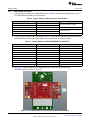
Board Description
Figure 16 shows the different sections of the TIDA-00339 design.
Power Supply
Options
VCC
LED
LDO
TPS7A1633
IO-Link PHY
SN65HVD102
Bypass
Protection
Protection
Circuitry
Interface
Connector
Status
Indication &
Connector
C/Q Current
Limiter
LaunchPad / BoosterPack
Connections
Manual SIO
Mode
Figure 16. TIDA-00339 Board Description
Power supply options
As described in Section 4.1, the design has several power supply options depending on the usage.
Table 5 shows the different settings of J1 and J2. For the initial setup, use Power Supply Option 2.
Table 5. Power Supply Options
TIDA-00339 POWER SUPPLY OPTIONS
J1
J2
COMMENTS
1
3.3 V from LaunchPad
X
-
The board gets its 3.3 V
from the connected
LaunchPad
2
3.3 V from TPS7A1633
-
X
The board gets its 3.3 V
from the LDO
(TPS7A1633)
3
3.3 V from TPS7A1633
while powering
LaunchPad
X
The board gets its 3.3 V
from the LDO
(TPS7A1633) and the
MCU of the connected
LaunchPad is also
powered by the LDO
X
VCC LED
LED D1 indicates the presence of VCC.
LDO – TPS7A1633
The linear voltage regulator circuit (in Power Supply Option 2 and Power Supply Option 3) generates the
3.3-V VCC from the 24 V of the IO-Link interface.
TIDU681A – January 2015 – Revised January 2015
Submit Documentation Feedback
Copyright © 2015, Texas Instruments Incorporated
IO-Link PHY BoosterPack
19
Getting Started
www.ti.com
IO-Link PHY – SN65HVD102
Circuitry of the IO-Link PHY.
Bypass protection
The user can bypass the on-board protection circuit by removing R3, R4, and R9. The entire protection is
removed, including M12 connector J3, and the IO-Link signals L+, L–, and C/Q must be applied through
J9. Note that in this case the reverse polarity is no longer available.
Protection circuitry
The design uses an additional transient protection circuitry consisting of the TVS diodes (D4, D5, and D6)
and bypass capacitors (C4, C5, and C7) to be in compliance with the IEC 61000-4-2, IEC 6100-4-4, and
IEC 6100-4-5 standards. Refer to Section 4.2 for more details on the protection circuitry.
Manual SIO Mode
Section to enable the manual SIO Mode and use switch S2 to toggle either NPN or PNP.
Table 6. SIO Mode Options
J6
J7
J8
DESCRIPTION
1-2
1-2
X
MCU control
2-3
2-3
1-2
Manual S2 control, NPN Mode
2-3
2-3
2-3
Manual S2 control, PNP Mode
LaunchPad and BoosterPack connectors
J10 and J12 are the connectors to interface TIDA-00339 to a LaunchPad. Please refer to the LaunchPad
in use to ensure proper connection between the devices. J10 and J12 have two long pins allowing the
connection of additional BoosterPacks on top of the TIDA-00339 device; for example, a display
BoosterPack or a sensor front-end BoosterPack.
C/Q current limiter
The circuitry changes between the resistor R10 (4.75 k) and potentiometer R11 (20 k) to allow individual
settings of the current limit of the C/Q line.
Table 7. Settings for Current Limit Options
J4
RESISTOR
DESCRIPTION
PINs 1-2 shorted
R11 active
20-k potentiometer → flexible adjustment of C/Q current limit
PINs 2-3 shorted
(default)
R10 active
4.75-k resistor → 250 mA
Status indication and connector
The status signals of the IO-Link PHY WAKE, TEMP OK, CURR OK, and PWR OK are available on J5
and indicated with LEDs D7, D8, D9, and D10. The output of those signals is an open drain output. In
case of a fault operation (warning or error) the GND switches to the respective J5 pins and the
corresponding LEDs illuminate. During normal operation the LEDs must be off.
Interface connector
The interface connector J11 can be used to connect an additional sensor front-end to the SPI of the MCU
of the connected LaunchPad. Connector J11 also monitors the communication interface between the IOLink PHY and the MCU. See Section 4.6 for more details.
20
IO-Link PHY BoosterPack
TIDU681A – January 2015 – Revised January 2015
Submit Documentation Feedback
Copyright © 2015, Texas Instruments Incorporated
Getting Started
www.ti.com
5.2
First Board Setup Manual SIO Mode
The initial board setup uses the TIDA-00339 in manual SIO Mode without the need of a connected
LaunchPad. In this mode, IO-Link communication is impossible.
Table 8. Jumper Setting for First Board Setup
5.3
5.3.1
JUMPER
SHORT
J1
Remove
J2
Set 1-2
J4
Set 2-3
J6
Set 2-3
J7
Set 2-3
J8
Set 1-2
COMMENTS
Power Supply Option 2 enabled
Resistor R10 (4.75k) active
Manual SIO Mode active
NPN selected
First Board Setup IO-Link Mode
Hardware and Software Requirements
For the initial setup the following hardware and software is required:
• TIDA-00339
• MSP-EXP430FR4133 LaunchPad
– IO-Link stack including the application firmware (4)
• USB IO-Link Master (this design uses the TMG – USB IO-Link Master V2 SE)
– GUI for USB IO-Link Master (this design uses the TMG IO-LINK Device Tool V4.0)
• IO Device Description (IODD) (4)
• M12 cable (female – male)
• USB cable
5.3.2
Software Installation
Please refer to the user manual of the USB IO-Link master in use for further details on its software
installation and how to import the IODD folder.
The following steps use the USB IO-Link Master V2 SE software from TMG (www.tmgte.com). The user
manual is available after installing the software, which is delivered along with the hardware. The user
manual describes the steps involved in importing the IODD files.
TIDU681A – January 2015 – Revised January 2015
Submit Documentation Feedback
Copyright © 2015, Texas Instruments Incorporated
IO-Link PHY BoosterPack
21
Getting Started
5.3.3
www.ti.com
Step-By-Step Description
1. Verify the jumper settings of the TIDA-00339 device (Table 9). Use the Power Supply Option 1 (3.3 V
for TIDA-00339 is provided by the LaunchPad).
Table 9. Jumper Settings for Board Setup in IO-Link Mode
JUMPER
SHORT
J1
Set 1-2
J2
Remove
J4
Set 2-3
J6
Set 1-2
J7
Set 1-2
J8
Don’t Care
COMMENTS
Power Supply Option 1 enabled
Resistor R10 (4.75 k) active
IO-Link Mode active
Only active in Manual SIO Mode
2. Verify the jumper settings of the LaunchPad (Table 10). This example uses the MSP-EXP430FR4133
LaunchPad. Please refer to the user’s guide of the LaunchPad in use for more details.
Table 10. Jumper Settings for MSP-EXP430FR4133 LaunchPad
CONNECTOR
JUMPER (SILKSCREEN)
SHORT
JP1
JP1
Set 1-2
J101
GND
Set
J101
5V
Set
J101
3V3
Set
J101
RTS
Remove
J101
CTS
Remove
J101
RXD
Set
J101
TXD
Set
J101
SBWTDIO
Set
J101
SBWTCK
Set
3. As Figure 17 shows, connect the TIDA-00339 device (J10 and J12 outer rows) to the
MSP-EXP430FR4133 device (J1 and J2).
Figure 17. Connection Between TIDA-00339 and MSP-EXP430FR4133
22
IO-Link PHY BoosterPack
TIDU681A – January 2015 – Revised January 2015
Submit Documentation Feedback
Copyright © 2015, Texas Instruments Incorporated
Getting Started
www.ti.com
4. Connect the PC through a USB cable to the LaunchPad J102 to power the system. If the LaunchPad is
not pre-programmed, please refer to the Software Section of the TIDA-00339 product folder (4).
5. Verify that the LED D1 of TIDA-00339 is on as soon as the system powers on.
6. Connect the TIDA-00339 (J3) to the IO-Link master.
7. Launch the USB IO-Link Master V2 software on the PC.
8. Follow the steps provided in the IO-Link Master user’s manual to establish a connection and import the
IODD files.
9. Figure 18 shows a screen-shot of the GUI after successfully establishing the connection.
10. Figure 19 shows the Process Data tab, which shows the content of the available variables.
Figure 18. IO-Link Master GUI After Established Connection to TIDA-00339
TIDU681A – January 2015 – Revised January 2015
Submit Documentation Feedback
Copyright © 2015, Texas Instruments Incorporated
IO-Link PHY BoosterPack
23
Getting Started
www.ti.com
Figure 19. IO-Link Master GUI—Process Data Tab
5.3.4
Usage
To reiterate, the objective of this TI design is to allow a flexible evaluation of the IO-Link interface with the
existing sensor front-ends. A connectable sensor front-end requires an MCU because of the flexibility of
the TIDA-00339 device. This MCU communicates with the MSP430 on the LaunchPad, exchanging the
data from the sensor to the IO-Link interface and vice versa (for configuring the sensor). Several variables
are available for this communication (INT32, INT16, and Bool1 to Bool8).
The default application “Stop-Watch” has been modified in the MSP-EXP430FR4133 firmware.
1. Stop-Watch Mode: The LaunchPad runs its default application “Stop-Watch” and the data sends
through the IO-Link interface to the IO-Link master and displays in the GUI. The sensor front-end is not
used in Stop-Watch Mode.
2. Temperature Mode: The LaunchPad runs its default application “Temperature” and the data sends
through the IO-Link interface to the IO-Link master and displays in the GUI. The sensor front-end is not
used in Temperature Mode.
3. Sensor Front-End Mode: The LaunchPad runs the additional “Sensor” and sends the data through the
IO-Link interface to the IO-Link master and displays the data in the GUI. A sensor front-end is required
in the Sensor Front-End Mode.
24
IO-Link PHY BoosterPack
TIDU681A – January 2015 – Revised January 2015
Submit Documentation Feedback
Copyright © 2015, Texas Instruments Incorporated
Design Files
www.ti.com
6
Design Files
6.1
Schematic
To download the schematic, see the design files at TIDA-00339.
VCC
J1
J2
1
2
2
1
2
VCC
3V3 from Launchpad
X
-
3V3 from LDO
-
X
3V3 from LDO + powering Launchpad
X
X
3
PG
C1
4.7 µF
4
9
GND
PAD
2
C2
0.47 µF
D2
Green
2
6
DNC
NC
J9
L+
LC/Q
TPS7A1633DRBR
GND
D1
Green
7
DELAY
GND
1
2
3
R2
68.1 Ω
GND
SN65HVD102 STATUS Signals
GND
VCC
VCC
0Ω
RF071M2S
C3
4.7 µF
R8
68.1 Ω
2
4
3
2
1
PWR_OK
CUR_OK
TEMP_OK
WAKE
1
VCCSET
5
15
19
16
PWR_OK
CUR_OK
TEMP_OK
WAKE
J5
NC
VCCIN
18
20
17
TX
EN
UART_RX
D10
Green
1
D9
Yellow
1
D8
Yellow
1
1
D7
Yellow
2
2
2
GND
8
7
4
L+
10
L+
CQ
12
C/Q
C5
DNPC6
330pF
2.2 µF
C4
0.1 µF
D5
SMAJ30CA
30 V
30 V
J3
R4
0Ω
TX
EN
RX
PWR_OK
CUR_OK
TEMP_OK
WAKE
LGND
GND
GND
PAD
ILIM_ADJ
NC
NC
NC
14
3
6
13
21
LC7
330 pF
3
R7
150 Ω
D4
SMAJ30CA
U2
R6
150 Ω
GND
D3
R3
VCC
R5
150 Ω
R1
68.1 Ω
1
J2
2
J1
LED
5
D6
SMAJ30CA
4
TIDA-00339 Power Options
SW
8
IN
EN
1
OUT
2
1
1
LDO_3V3
VCC
3V3
1
S1
U1
30 V
R9
2
11
9
0Ω
SN65HVD102RGBR
GND
Current Limiter Options
Manual SIO Mode
LaunchPad / BoosterPack Connectors
J4
GND
3V3
UART_RX
UART_TX
ENBL
R10
4.75 kΩ
R11
20 kΩ
VCC
J8
1
2
3
1
3
5
7
9
11
13
15
17
19
1
2
3
J12
2
4
6
8
10
12
14
16
18
20
J7
3
2
1
UART_TX
TX
SPI_CLK
CUR_OK
GND
GND
GND
J6
1
2
3
VCC
J10
1
3
5
7
9
11
13
15
17
19
2
4
6
8
10
12
14
16
18
20
Sensor-Front Interface / MCU-IOLINK PHY communication
TEMP_OK
SPI_CS1
SW
SPI_MOSI
SPI_MISO
LED
PWR_OK
WAKE
J11
GND
3V3
UART_TX
UART_RX
ENBL
9
7
5
3
1
10
8
6
4
2
1
ENBL
SPI_CLK
SPI_MISO
SPI_MOSI
SPI_CS1
GND
S2
2
EN
R12
10.0 k
GND
Figure 20. Schematic
TIDU681A – January 2015 – Revised January 2015
Submit Documentation Feedback
IO-Link PHY BoosterPack
Copyright © 2015, Texas Instruments Incorporated
25
Design Files
6.2
www.ti.com
Bill of Materials
To download the bill of materials (BOM), see the design files at TIDA-00339.
Table 11. BOM
ITEM #
26
DESIGNATOR
QUANTITY
PART NUMBER
MANUFACTURER
TIDA-00339
Any
4.7 µF
GRM21BR71A475KA73L
MuRata
CAP, CERM, 4.7 µF, 10 V, ±10%,
X7R, 0805
0805
1
0.47 µF
GRM21BR72A474KA73L
MuRata
CAP, CERM, 0.47 µF, 100 V,
±10%, X7R, 0805
0805
C3
1
4.7 µF
C1005X5R0J475M050BC
TDK
CAP, CERM, 4.7 µF, 6.3 V, ±20%,
X5R, 0402
0402
5
C4
1
0.1 µF
12061C104JAT2A
AVX
CAP, CERM, 0.1 µF, 100 V, ±5%,
X7R, 1206
1206
6
C5
1
2.2 µF
GRM32ER72A225KA35L
MuRata
CAP, CERM, 2.2 µF, 100 V, ±10%,
X7R, 1210
1210
7
C7
1
330 pF
GRM155R72A331KA01D
MuRata
CAP, CERM, 330 pF, 100 V, ±10%,
X7R, 0402
0402
8
D1, D2, D10
3
Green
150060VS75000
Wurth Elektronik eiSos
1
!PCB1
1
2
C1
1
3
C2
4
VALUE
200 V
RF071M2S
DESCRIPTION
PACKAGE REFERENCE
Printed Circuit Board
LED, Green, SMD
LED_0603
Rohm
Diode, Ultrafast, 200 V, 1 A, SOD123
SOD-123
Diode, TVS, Bi, 30 V, 400 W, SMA
9
D3
1
10
D4, D5, D6
3
30 V
SMAJ30CA
Littelfuse
11
D7, D8, D9
3
Yellow
150060YS75000
Wurth Elektronik eiSos
12
FID1, FID2, FID3
3
N/A
N/A
Fiducial mark. There is nothing to
buy or mount.
Fiducial
13
J1, J2
2
61300211121
Wurth Elektronik eiSos
Header, 2.54 mm, 2 x 1, Gold, TH
Header, 2.54 mm, 2 x 1,
TH
14
J3
1
43-01205
Conec
M12 Socket, Backmounting, 4Pos,
Gold, R/A, TH
M12 Socket,
Backmounting, 4Pos, R/A,
TH
15
J4, J6, J7, J8, J9
5
61300311121
Wurth Elektronik eiSos
Header, 2.54 mm, 3 x 1, Gold, TH
Header, 2.54 mm, 3 x 1,
TH
16
J5
1
61300411121
Wurth Elektronik eiSos
Header, 2.54 mm, 4 x 1, Gold, TH
Header, 2.54 mm, 4 x 1,
TH
17
J10, J12
2
SSW-110-23-F-D
Samtec
Connector, Receptacle, 100 mil, 10
x 2, Gold plated, TH
10 x 2 Receptacle
18
J11
1
61301021121
Wurth Elektronik eiSos
Header, 2.54 mm, 5 x 2, Gold, TH
Header, 2.54 mm, 5 x 2,
TH
19
R1, R2, R8
3
68.1
CRCW040268R1FKED
Vishay-Dale
RES, 68.1, 1%, 0.063 W, 0402
0402
20
R3, R4, R9
3
0
CRCW08050000Z0EAHP
Vishay-Dale
RES, 0, 5%, 0.333 W, 0805
0805
21
R5, R6, R7
3
150
CRCW0402150RFKED
Vishay-Dale
RES, 150, 1%, 0.063 W, 0402
0402
IO-Link PHY BoosterPack
LED, Yellow, SMD
SMA
LED_0603
TIDU681A – January 2015 – Revised January 2015
Submit Documentation Feedback
Copyright © 2015, Texas Instruments Incorporated
Design Files
www.ti.com
Table 11. BOM (continued)
ITEM #
QUANTITY
VALUE
PART NUMBER
MANUFACTURER
22
R10
DESIGNATOR
1
4.75 kΩ
CRCW08054K75FKEA
Vishay-Dale
DESCRIPTION
23
R11
1
20 kΩ
3224J-1-203 E
Bourns
24
R12
1
10.0 kΩ
CRCW040210K0FKED
Vishay-Dale
RES, 10.0 kΩ, 1%, 0.063 W, 0402
0402
25
S1, S2
2
434121025816
Wurth Elektronik eiSos
Switch, Tactile, SPST, 12 V, SMD
SMD, 6 x 3.9 mm
26
U1
1
TPS7A1633DRBR
Texas Instruments
27
U2
1
SN65HVD102RGBR
Texas Instruments
IO-LINK PHY for Device Nodes,
RGB0020A
28
C6
0
GRM155R72A331KA01D
MuRata
TIDU681A – January 2015 – Revised January 2015
Submit Documentation Feedback
0805
TRIMMER, 20 kΩ, 0.25 W, SMD
60-V, 5-µA IQ, 100-mA,
Low-Dropout Voltage Regulator
With Enable and Power-Good,
DRB0008B
330 pF
PACKAGE REFERENCE
RES, 4.75 kΩ, 1%, 0.125 W, 0805
4.8 x 3.71 x 4.6 mm
CAP, CERM, 330 pF, 100 V, ±10%,
X7R, 0402
DRB0008B
RGB0020A
0402
IO-Link PHY BoosterPack
Copyright © 2015, Texas Instruments Incorporated
27
Design Files
6.3
www.ti.com
Layer Plots
To download the layer plots, see the design files at TIDA-00339.
28
Figure 21. Top Overlay
Figure 22. Top Solder Mask
Figure 23. Top Layer
Figure 24. Midlayer 1
Figure 25. Midlayer 2
Figure 26. Bottom Layer
Figure 27. Bottom Solder Mask
Figure 28. Bottom Overlay
IO-Link PHY BoosterPack
TIDU681A – January 2015 – Revised January 2015
Submit Documentation Feedback
Copyright © 2015, Texas Instruments Incorporated
Design Files
www.ti.com
Figure 29. Drill Drawing
Figure 30. Board Outline
TIDU681A – January 2015 – Revised January 2015
Submit Documentation Feedback
Copyright © 2015, Texas Instruments Incorporated
IO-Link PHY BoosterPack
29
Design Files
6.4
www.ti.com
Assembly Drawings
Figure 31. Top Assembly Drawing
6.5
Figure 32. Bottom Assembly Drawing
PCB and Layout Guidelines
The form-factor of the PCB has been chosen to fit on existing MSP430 LaunchPads. The PCB of the
TIDA-00339 device extends to the left and right sides instead of the top and bottom sides. This setup
allows the user to operate any existing buttons and visual indicators like LEDs and displays on the
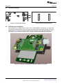
LaunchPad. Figure 33 shows a 3D plot of the TI design connected to the MSP430 LaunchPad.
Figure 33. 3D-Plot of TIDA-00339 Connected to MSP430 LaunchPad
30
IO-Link PHY BoosterPack
TIDU681A – January 2015 – Revised January 2015
Submit Documentation Feedback
Copyright © 2015, Texas Instruments Incorporated
Software Files
www.ti.com
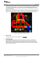
TI recommends to place the protection circuitry close to the M12 connector (J3). The TVS diodes D4, D5,
and D6 have been placed directly at J3, which enables the immediate clamping of potential high currents,
according to the TVS specifications. Figure 34 shows a circuit snippet highlighting the three signals
L+, L–, and C/Q going from J3 to the TVS diodes. In this view, the VCC and GND plane, as well as the
polygons, were disabled.
Depending on the use for SN65HVD101 (U2), a proper thermal design is required, especially when the
device is used in the SIO Mode. According to the datasheet, a residual voltage across the driver low-side
switch of 3.5 V can be present for a current of 250 mA, resulting in a power dissipation of 875 mW.
Figure 34. Layout of the Protection Circuitry
7
Software Files
To download the software files, see the design files at TIDA-00339.
8
About the Author
ALEXANDER WEILER is a systems engineer at Texas Instruments, where he is responsible for
developing reference design solutions for the industrial segment. Alexander brings to this role his
extensive experience in high-speed digital, low-noise analog, and RF system-level design expertise.
Alexander earned his diploma in electrical engineering (Dipl.-Ing. (FH)) from the University of Applied
Science in Karlsruhe, Germany.
TIDU681A – January 2015 – Revised January 2015
Submit Documentation Feedback
Copyright © 2015, Texas Instruments Incorporated
IO-Link PHY BoosterPack
31
IMPORTANT NOTICE FOR TI REFERENCE DESIGNS
Texas Instruments Incorporated ("TI") reference designs are solely intended to assist designers (“Buyers”) who are developing systems that
incorporate TI semiconductor products (also referred to herein as “components”). Buyer understands and agrees that Buyer remains
responsible for using its independent analysis, evaluation and judgment in designing Buyer’s systems and products.
TI reference designs have been created using standard laboratory conditions and engineering practices. TI has not conducted any
testing other than that specifically described in the published documentation for a particular reference design. TI may make
corrections, enhancements, improvements and other changes to its reference designs.
Buyers are authorized to use TI reference designs with the TI component(s) identified in each particular reference design and to modify the
reference design in the development of their end products. HOWEVER, NO OTHER LICENSE, EXPRESS OR IMPLIED, BY ESTOPPEL
OR OTHERWISE TO ANY OTHER TI INTELLECTUAL PROPERTY RIGHT, AND NO LICENSE TO ANY THIRD PARTY TECHNOLOGY
OR INTELLECTUAL PROPERTY RIGHT, IS GRANTED HEREIN, including but not limited to any patent right, copyright, mask work right,
or other intellectual property right relating to any combination, machine, or process in which TI components or services are used.
Information published by TI regarding third-party products or services does not constitute a license to use such products or services, or a
warranty or endorsement thereof. Use of such information may require a license from a third party under the patents or other intellectual
property of the third party, or a license from TI under the patents or other intellectual property of TI.
TI REFERENCE DESIGNS ARE PROVIDED "AS IS". TI MAKES NO WARRANTIES OR REPRESENTATIONS WITH REGARD TO THE
REFERENCE DESIGNS OR USE OF THE REFERENCE DESIGNS, EXPRESS, IMPLIED OR STATUTORY, INCLUDING ACCURACY OR
COMPLETENESS. TI DISCLAIMS ANY WARRANTY OF TITLE AND ANY IMPLIED WARRANTIES OF MERCHANTABILITY, FITNESS
FOR A PARTICULAR PURPOSE, QUIET ENJOYMENT, QUIET POSSESSION, AND NON-INFRINGEMENT OF ANY THIRD PARTY
INTELLECTUAL PROPERTY RIGHTS WITH REGARD TO TI REFERENCE DESIGNS OR USE THEREOF. TI SHALL NOT BE LIABLE
FOR AND SHALL NOT DEFEND OR INDEMNIFY BUYERS AGAINST ANY THIRD PARTY INFRINGEMENT CLAIM THAT RELATES TO
OR IS BASED ON A COMBINATION OF COMPONENTS PROVIDED IN A TI REFERENCE DESIGN. IN NO EVENT SHALL TI BE
LIABLE FOR ANY ACTUAL, SPECIAL, INCIDENTAL, CONSEQUENTIAL OR INDIRECT DAMAGES, HOWEVER CAUSED, ON ANY
THEORY OF LIABILITY AND WHETHER OR NOT TI HAS BEEN ADVISED OF THE POSSIBILITY OF SUCH DAMAGES, ARISING IN
ANY WAY OUT OF TI REFERENCE DESIGNS OR BUYER’S USE OF TI REFERENCE DESIGNS.
TI reserves the right to make corrections, enhancements, improvements and other changes to its semiconductor products and services per
JESD46, latest issue, and to discontinue any product or service per JESD48, latest issue. Buyers should obtain the latest relevant
information before placing orders and should verify that such information is current and complete. All semiconductor products are sold
subject to TI’s terms and conditions of sale supplied at the time of order acknowledgment.
TI warrants performance of its components to the specifications applicable at the time of sale, in accordance with the warranty in TI’s terms
and conditions of sale of semiconductor products. Testing and other quality control techniques for TI components are used to the extent TI
deems necessary to support this warranty. Except where mandated by applicable law, testing of all parameters of each component is not
necessarily performed.
TI assumes no liability for applications assistance or the design of Buyers’ products. Buyers are responsible for their products and
applications using TI components. To minimize the risks associated with Buyers’ products and applications, Buyers should provide
adequate design and operating safeguards.
Reproduction of significant portions of TI information in TI data books, data sheets or reference designs is permissible only if reproduction is
without alteration and is accompanied by all associated warranties, conditions, limitations, and notices. TI is not responsible or liable for
such altered documentation. Information of third parties may be subject to additional restrictions.
Buyer acknowledges and agrees that it is solely responsible for compliance with all legal, regulatory and safety-related requirements
concerning its products, and any use of TI components in its applications, notwithstanding any applications-related information or support
that may be provided by TI. Buyer represents and agrees that it has all the necessary expertise to create and implement safeguards that
anticipate dangerous failures, monitor failures and their consequences, lessen the likelihood of dangerous failures and take appropriate
remedial actions. Buyer will fully indemnify TI and its representatives against any damages arising out of the use of any TI components in
Buyer’s safety-critical applications.
In some cases, TI components may be promoted specifically to facilitate safety-related applications. With such components, TI’s goal is to
help enable customers to design and create their own end-product solutions that meet applicable functional safety standards and
requirements. Nonetheless, such components are subject to these terms.
No TI components are authorized for use in FDA Class III (or similar life-critical medical equipment) unless authorized officers of the parties
have executed an agreement specifically governing such use.
Only those TI components that TI has specifically designated as military grade or “enhanced plastic” are designed and intended for use in
military/aerospace applications or environments. Buyer acknowledges and agrees that any military or aerospace use of TI components that
have not been so designated is solely at Buyer's risk, and Buyer is solely responsible for compliance with all legal and regulatory
requirements in connection with such use.
TI has specifically designated certain components as meeting ISO/TS16949 requirements, mainly for automotive use. In any case of use of
non-designated products, TI will not be responsible for any failure to meet ISO/TS16949.IMPORTANT NOTICE
Mailing Address: Texas Instruments, Post Office Box 655303, Dallas, Texas 75265
Copyright © 2015, Texas Instruments Incorporated