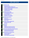
1
ECED 3204. Microprocessors
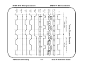
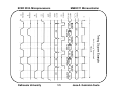
Transparencies
ECED 3204. Microprocessors
TRANSPARENCIES
Instructor: Jose Gonzalez-Cueto
Department of Electrical & Computer Engineering
Dalhousie University, Halifax
Fall 2013
Dalhousie University
1
Jose A. Gonzalez-Cueto
ECED 3204. Microprocessors
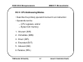
Introduction to the Course
Course website:
http://myweb.dal.ca/~gonzalej/Teaching/Eced3204/ECED3204.html
(or) Dept webpage → Faculty → Jose → Teaching → Microprocessors
Hardware:
1. Motorola M68HC11EVB board (The evaluation board or EVB)
– Based on the M68HC11 MCU (MicroController Unit)
Software:
1. Mini IDE (Integrated Development Environment, Runs on PC)
– M68HC11 Cross Assembler
– Building executable files
– Downloading of 6811 executables to the EVB
– PC ↔ EVB serial communication
Dalhousie University
2
Jose A. Gonzalez-Cueto
ECED 3204. Microprocessors
Introduction to the Course
Software (Cont’d):
2. Stan Simmons’ QEVB11 Simulator (Runs on PC)
– Simulates the EVB board in detail
– CPU operation, bus timing, serial communication and more...
– Downloadable through link in course website
– Comes with tutorials. Do tutorials 1-3 over weeks 1-4
– Helpful for the Labs, program debugging and testing
Dalhousie University
3
Jose A. Gonzalez-Cueto
ECED 3204. Microprocessors
Introduction to the Course
Bibliography
[1] Hughes, L., Hardware and Software Design for the MC68HC11,
5th edition, Whale Lake Press, 2004 (textbook) - REQUIRED.
[2] M68HC11 Reference Manual, a.k.a. The Pink Book , Motorola.
[3] MC68HC11A8 Programming Reference Guide, Motorola - REQUIRED.
[4] M68HC11EVB Evaluation Board User's Manual, Motorola.
[5] Huang, H., MC68HC11: An Introduction; Software and Hardware
Interfacing , 2nd edition, Delmar Thomson Learning, 2000
(textbook) (in Library & Bookstore) - REQUIRED.
[6] Gonzalez-Cueto, J.A., ECED3204 Transparencies, April 2006 - REQUIRED.
[7] Martin, F., Introduction to 6811 Programming , Media Lab, MIT.
[8] Spasov, P., Microcontroller Technology: The 68HC11, 4th edition, Prentice
Hall, 2002.
[9] Driscoll, Coughlin & Villanucci, Data Acquisition and Process Control with
the M68HC11 Microcontroller, Merril / Macmillan, 1994 (in Library).
Dalhousie University
4
Jose A. Gonzalez-Cueto
ECED 3204. Microprocessors
Introduction to the Course
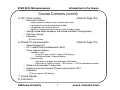
Course Contents
1. Introduction to the course.
2. Introductory topics,
–
–
–
–
–
–
–
–
(Starts on Page 2)
(Starts on Page 9)
Basic computer architecture (CPU, memory, I/O components and buses).
Numeric systems; decimal, binary, hexadecimal.
Representation of information in memory, the byte.
Different formats: unsigned, signed, ASCII characters and BCD representation.
Memory architectures, memory segments from a programming point of view.
Memory modules and its interaction with the address, data and control buses.
The central processing unit (CPU), instruction cycle and CPU registers.
I/O components, device polling and interrupts.
3. The Motorola 68HC11 MicroController Unit (MCU),
–
–
–
–
–
–
–
–
–
–
–
–
–
(Starts on Page 27)
Microprocessors vs microcontrollers.
The 68HC11A8 architecture, pin description, operation modes.
Address space and memory map of the 68HC11A8 MCU.
Introduction to the 68HC11 I/O components (Ports A-E).
CPU: Registers, addressing mode, instruction set.
Assembly language programming for the 68HC11 MCU, assembler directives.
The development process (assembler, linker, librarian and loader), Motorola S-record files.
The 68HC11EVB evaluation board, memory map, monitor program, BUFFALO commands.
Allocation of external memory modules. Using decoders - the 74HC138.
Demultiplexing address and data buses - the 74HC373 latch.
The bus cycle. RAM/EPROM read cycles. RAM write cycle. Timing diagrams.
Cycle-by-cycle CPU execution. Register transfer notation.
Laboratories
(1) Introduction to the M68HC11EVB,
(2) Assembly language programming, and
(3) Instruction execution, bus cycle & timing diagrams.
Dalhousie University
5
Jose A. Gonzalez-Cueto
ECED 3204. Microprocessors
Introduction to the Course
Course Contents (cont’d)
4. Asynchronous serial communication,
–
Introduction,
•
•
•
•
•
–
EVB connectors, EVB serial port connectors.
The SCI and ACIA as the EVB UARTs.
Use of the D-type flipflop and digital switches.
ACIA decode & programming.
BUFFALO communication, the RS232 window (SCI terminal) and EVB ports.
RS232 drivers & receivers.
Interrupts,
•
•
•
–
SCI tx unit.
SCI rx unit. Error handling.
Control/status registers, rx/tx data registers.
CPU «--» SCI unit interaction, I/O methods: polling & interrupts.
Asynchronous serial communication and the EVB,
•
•
•
•
•
•
–
UART rx & tx units.
Registers and character formation/handling in both directions.
Serial-to-parallel, parallel-to-serial conversion processes.
Errors and error handling.
The RS-232 standard.
The HC11 and asynchronous serial communication .- the SCI unit,
•
•
•
•
–
(Starts on Page 126)
The HC11 interrupt vector table.
Interrupt driven I/O, programming with interrupts.
Interrupts and the M68HC11EVB evaluation board.
Laboratories,
(4) Device polling & terminal I/O,
(5) Asynchronous serial communication and interrupts.
Dalhousie University
6
Jose A. Gonzalez-Cueto
ECED 3204. Microprocessors
Introduction to the Course
Course Contents (cont’d)
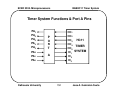
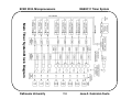
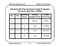
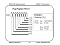
5. HC11 timer system,
(Starts at Page 152)
– Main timer functions
•
•
•
•
Output compare; software timing, waveform generation.
Input capture; measuring period & pulse width.
Long periods and counter overflows.
Algorithms for generating and measuring slow-changing signals.
– Solving missed output compares and missed overflows. Interrupt priority.
– Real-time interrupt.
– Laboratory:
(6) Timer functions.
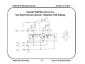
6. Parallel I/O communication,
(Starts at Page 170)
– General purpose I/O.
– HC11 output PortB and bidirectional PortC.
– Seven segment displays.
• Hardware issues
– Using HC11 ports to light 7-segment LED displays.
– Controlling multiple 7-segment displays.
• Software issues
– Light patterns for digits to be displayed. Table lookup.
– Conversion of 16-bit hex format --» BCD format «--» ASCII-coded decimal format.
– Strobe and handshake I/O subsystem.
– Design and service of parallel I/O ports external to the HC11.
– Laboratory:
(7) Seven-segment LED displays.
7. Course Review.
8. Final Exam.
Dalhousie University
7
Jose A. Gonzalez-Cueto
ECED 3204. Microprocessors
Introduction to the Course
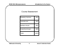
Course Assessment
Biweekly Quizzes:
25%
Laboratories:
25%
MidTerm Exam
25%
EndofTerm Exam
25%
Total:
Dalhousie University
100%
8
Jose A. Gonzalez-Cueto
ECED 3204. Microprocessors
Introductory Topics
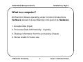
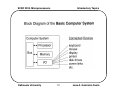
What is a computer?
An Electronic Device operating under Control of Instructions
(Software) stored in its own Memory Unit (part of its Hardware)
1. Accepts Data (Input)
2. Processes Data Arithmetically / Logically
3. Displays Information from the processing (Output)
4. Stores results for future use
Dalhousie University
9
Jose A. Gonzalez-Cueto
ECED 3204. Microprocessors
Dalhousie University
Introductory Topics
10
Jose A. Gonzalez-Cueto
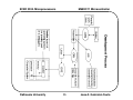
ECED 3204. Microprocessors
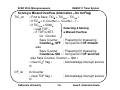
Introductory Topics
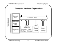
PROCESSOR
Computer Hardware Organization
Control
Unit
Common BUS
Arithmetic
Logic
Unit
Registers
Dalhousie University
MEMORY
Program Data
Storage Storage
11
Output
Input
Unit(s)
Unit(s)
Jose A. Gonzalez-Cueto
ECED 3204. Microprocessors
Introductory Topics
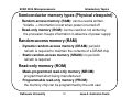
Semiconductor memory types (Physical viewpoint)
- Random-access memory (RAM): can be read & written.
Volatile -> information is lost when power is turned off
- Read-only memory (ROM): can be read but not written by
the processor. Keeps information in absence of power supply
Random-access memory (RAM)
- Dynamic random-access memory (DRAM): periodic
refresh is required to maintain the contents of a DRAM chip
- Static random-access memory (SRAM): no periodic
refresh is required
Read-only memory (ROM)
- Mask-programmed read-only memory (MROM):
programmed when being manufactured
- Programmable read-only memory (PROM):
the memory chip can be programmed by the end user
Dalhousie University
12
Jose A. Gonzalez-Cueto
ECED 3204. Microprocessors
-
Introductory Topics
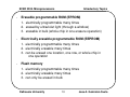
Erasable programmable ROM (EPROM)
1. electrically programmable many times
2. erased by ultraviolet light (through a window)
3. erasable in bulk (whole chip in one erasure operation)
-
Electrically erasable programmable ROM (EEPROM)
1. electrically programmable many times
2. electrically erasable many times
3. can be erased one location, one row, or whole chip in
one operation
-
Flash memory
1. electrically programmable many times
2. electrically erasable many times
3. can only be erased in bulk
Dalhousie University
13
Jose A. Gonzalez-Cueto
ECED 3204. Microprocessors
Introductory Topics
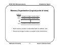
Memory Organization (Logical point of view)
Address
0000 Contents of Mem Location 0000
0001
Contents of Mem Location 0001
nnnn
Contents of Mem Location nnnn
• Each memory location is associated with an address, and
• Serves as storage for data or program code (instructions)
Dalhousie University
14
Jose A. Gonzalez-Cueto
ECED 3204. Microprocessors
Introductory Topics
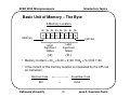
Basic Unit of Memory – The Byte
A Memory Location
B7 B6 B5 B4 B3 B2 B1 B0
0 1
0
0
1
1
0
0
MSB (B7)
LSB (B0)
Most
Significant
Nibble
Least
Significant
Nibble
(4)
(C)
• Memory Content = 4CH = $ 4C = 0100 1100B = % 0100 1100
• If the content of this memory location is interpreted by the CPU as
an instruction:
Machine Code
$4C
Dalhousie University
Assembler Code
=
INCA
15
Jose A. Gonzalez-Cueto
ECED 3204. Microprocessors
Introductory Topics
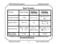
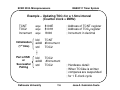
Data Formats
1-Byte Range
Example 1
0100 1000b
Example 2
1100 1010b
0..255d
64 + 8 = 72d
128+ 64+ 8+ 2 =
202d
Signed number
-128..127d
72d
ASCII character
<NUL>..<DEL>
00 .. 127d
48h = ‘H’
(Table lookup)
out-of-range (∗), or
If B7, 4Ah = ‘J’
Binary-coded
decimal (BCD)
00..99d
48d
<invalid>
Formats
Unsigned number
− 0011 0110b =
− 36h = − 54d
(∗) 202d = ‘╩’, See http://www.lookuptables.com/ for Extended ASCII codes
Dalhousie University
16
Jose A. Gonzalez-Cueto
ECED 3204. Microprocessors
Introductory Topics
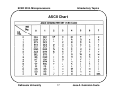
ASCII Chart
Dalhousie University
17
Jose A. Gonzalez-Cueto
ECED 3204. Microprocessors
Introductory Topics
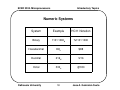
Numeric Systems
System
Example
HC11 Notation
Binary
1101 1000b
%1101 1000
Hexadecimal
D8h
$D8
Decimal
216d
!216
Octal
330o
@330
Dalhousie University
18
Jose A. Gonzalez-Cueto
ECED 3204. Microprocessors
Introductory Topics
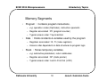
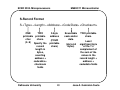
Memory Segments
•
Program : Contains program instructions,
– e.g. operation codes (OpCodes), instruction operands
– Register associated : PC (program counter)
– Typical access order: Top-to-bottom
•
Data : Holds constants & variables used by the program
– Registers associated : IX, IY (index registers)
– Access order dependent on data structures & program logic
•
Stack : Stores temporary variables,
– e.g. subroutine parameters, return addresses
– Register associated : SP (stack pointer)
– Typical access order: Last-In First-Out (LIFO)
Dalhousie University
19
Jose A. Gonzalez-Cueto
ECED 3204. Microprocessors
Introductory Topics
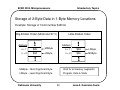
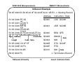
Storage of 2-Byte Data in 1-Byte Memory Locations
Example: Storage of 16-bit number $ 2E 0A
Big-Endian Order (Motorola HC11)
Little-Endian Order
Address
Address
n+1
$2E
MSByte
n+1
$0A
LSByte
n+2
$0A
LSByte
n+2
$2E
MSByte
MSByte − Most Significant Byte
Valid for all memory segments:
LSByte − Least Significant Byte
Program, Data & Stack
Dalhousie University
20
Jose A. Gonzalez-Cueto
ECED 3204. Microprocessors
Introductory Topics
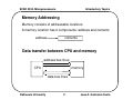
Memory Addressing
Memory consists of addressable locations
A memory location has 2 components: address and contents
address
contents
Data transfer between CPU and memory
address bus lines
CPU
memory
data bus lines
Dalhousie University
21
Jose A. Gonzalez-Cueto
ECED 3204. Microprocessors
Introductory Topics
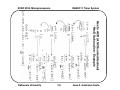
A0
A1
D0
D1
CPU D7
A12
A13
R/W
A15
Clock
Data
Bus
(D0 - D7)
Memory
D0 Module
D1
D7
W
A0
A1
8K x 8
RAM A12
OE (G)
E
A2
A1
A0
D
e
c
o
d
e Y7
r
Y0
Y1
CS (E)
CS
To Another
Memory
Module
Address Bus (A0 - A12)
Dalhousie University
22
Jose A. Gonzalez-Cueto
ECED 3204. Microprocessors
Introductory Topics
Busses
• Address Bus
– Set of parallel lines used to specify a memory location
– Unidirectional (CPU → Memory)
– # lines = # bits required to address all memory locations.
• e.g. For an 8K memory module, 8K = 23 x 210 = 213 locations
• Hence, 13 lines are required
• Data Bus
– Set of parallel lines carrying data / instructions
• e.g. An 8-bit CPU can transfer 8 bits (1byte) of data at a time
– Bidirectional (CPU ↔ Memory)
• Control Bus
– Set of lines controlling data transfer
– Example of lines
• CS: chip selection logic
• Clock : synch signal,
• R/W : Read or Write
Dalhousie University
Unidirectional (CPU → Memory)
23
Jose A. Gonzalez-Cueto
ECED 3204. Microprocessors
Introductory Topics
Exercise: Provide this 8-bit CPU with a 64Kbyte Memory Space
16
Address Bus (A15 – A0)
__
A__- A__
A__- A__
32K x 4
D__- D__
8-bit
CPU
__
__
A__- A__
32K x 4
__
D__- D__
CS
32K x 4
__
D__- D__
CS
__
CS
__
__
A__- A__
A__- A__
32K x 4
D__- D__
A__- A__
32K x 4
__
D__- D__
CS
__
CS
32K x 4
__
D__- D__
__
CS
8
Data Bus (D7 – D0)
Note : The Clock (Ck) & R/W signals have been omitted for simplicity
Dalhousie University
24
Jose A. Gonzalez-Cueto
ECED 3204. Microprocessors
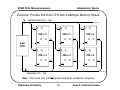
Introductory Topics
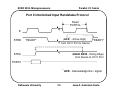
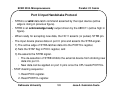
I/O Schemes
1.Isolated I/O scheme
- The microprocessor has dedicated instructions for I/O operations
- The microprocessor has a separate address space for I/O devices
2.Memory-mapped I/O scheme
- The microprocessor uses the same instruction set for I/O operations
- The I/O devices and memory components are resident in the same
memory space
Dalhousie University
25
Jose A. Gonzalez-Cueto
ECED 3204. Microprocessors
Introductory Topics
Synchronizing the Microprocessor and the Interface Chip
The polling method
1.for input -- the microprocessor checks a status bit of the
interface chip to find out if the interface chip has received new data
from the input device.
2.for output -- the microprocessor checks a status bit of the
interface chip to find out if it can send new data to the interface chip.
The interrupt-driven method
1.for input -- the interface chip interrupts the microprocessor
whenever it has received new data from the input device.
2.for output -- the interface chip interrupts the microprocessor
whenever it can accept new data from the microprocessor.
Dalhousie University
26
Jose A. Gonzalez-Cueto
ECED 3204. Microprocessors
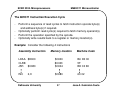
M68HC11 Microcontroller
Motorola S-Records
• Files containing Machine Code (“∗.s19”)
• ASCII files - portable (edited on any PC)
• Readable
– Hex machine code
– Memory addresses where code will be loaded
Dalhousie University
27
Jose A. Gonzalez-Cueto
ECED 3204. Microprocessors
M68HC11 Microcontroller
S-Record Format
S <Type> <Length> <Address> <Code/Data> <Checksum>
ONE
TWO
printable printable
char
chars.
(0..9)
Specify the
record
length in
bytes,
counting
address +
code/data +
checksum
fields
Dalhousie University
2-byte
address
(FOUR
printable
chars)
28
Executable
code and/or
data.
(Up to 64
bytes)
TWO printable
chars.
Least
significant byte
of the 1’s
complement of
the sum of the
values in the
record length +
address +
code/data fields
Jose A. Gonzalez-Cueto
ECED 3204. Microprocessors
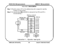
M68HC11 Microcontroller
S-Record Example
S0 0E 0000 53 52 45 43 4F 52 44 2E 42 41 4B E3 ⇐ Starting Record
Address
Instruction / Data
$C000
LDX $C008
$C003
JSR $C00B
S1 09 C006 20 FE 00 0A 05 FF 04
$C006
BRA $FE
Type
$C008
$000A
$C00A
$05
S1 05 C00C C0 0F 5F
$C00B
STX $C00F
S1 04 C00E 39 F4
$C00E
RTS
S1 04 C010 00 2B
$C010
$00
S1 04 C000 FE 3D
S1 05 C001 C0 08 71
S1 04 C003 BD 7B
S1 05 C004 C0 0B 6B
Address
Length
Checksum
Code / Data
S9 03 0000 FC
Dalhousie University
Data
Data
⇐ Termination Record
29
Jose A. Gonzalez-Cueto
ECED 3204. Microprocessors
M68HC11 Microcontroller
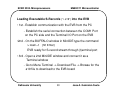
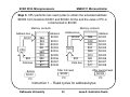
Loading Executable S-Records (“∗.s19”) into the EVB
• 1st - Establish communication with the EVB from the PC
- Establish the serial connection between the COM1 Port
on the PC side and the Terminal I/O Port on the EVB
•2nd - On the BUFFALO window in MiniIDE type the command
> load –t {hit Enter}
EVB ready for S-record stream through (t)erminal port
• 3rd - Open a 2nd MiniIDE window and connect it as a
Terminal window
- Go to Menu Terminal -> Download File -> Browse for the
.s19 file to download to the EVB board
Dalhousie University
30
Jose A. Gonzalez-Cueto
ECED 3204. Microprocessors
M68HC11 Microcontroller
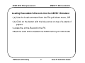
Loading Executable S-Records into the QEVB11 Simulator
• (a) Use the Load command from the File pull-down menu, OR
• (b) Click on the button with the blue arrow on top of a stack of
papers
• Locate the .s19 s-Record in the PC
• Machine code will be loaded into RAM memory of EVB model
Dalhousie University
31
Jose A. Gonzalez-Cueto
ECED 3204. Microprocessors
Dalhousie University
M68HC11 Microcontroller
32
Jose A. Gonzalez-Cueto
ECED 3204. Microprocessors
Dalhousie University
M68HC11 Microcontroller
33
Jose A. Gonzalez-Cueto
ECED 3204. Microprocessors
Dalhousie University
M68HC11 Microcontroller
34
Jose A. Gonzalez-Cueto
ECED 3204. Microprocessors
Dalhousie University
M68HC11 Microcontroller
35
Jose A. Gonzalez-Cueto
ECED 3204. Microprocessors
M68HC11 Microcontroller
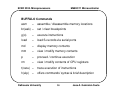
BUFFALO Commands
asm
–
assemble / disassemble memory locations
br(eak) –
set / clear breakpoints
g(o)
–
execute instructions
load
–
load S-records via serial ports
md
–
display memory contents
mm
–
view / modify memory contents
p
–
proceed / continue execution
rm
–
view / modify contents of CPU registers
t(race) –
trace execution of instructions
h(elp)
offers commands’ syntax & brief description
–
Dalhousie University
36
Jose A. Gonzalez-Cueto
ECED 3204. Microprocessors
Dalhousie University
M68HC11 Microcontroller
37
Jose A. Gonzalez-Cueto
$0000
$00FF
$1000
$103F
$B600
RAM
I/O REGISTERS
EEPROM
¥
¥
External (Available)
∗
External (Available)
∗
External (Available)
∗
HC11 Memory Map
$B7FF
$E000
ROM
$FFC0
INTERRUPT VECTOR
$FFFF
256 Bytes
64 Bytes
512 Bytes
8 KBytes
Either or both internal ROM & EEPROM can be disabled
∗ External Memory has a meaning only for Expanded Mode
¥
Jose A. Gonzalez-Cueto
38
Dalhousie University
M68HC11 Microcontroller
ECED 3204. Microprocessors
ECED 3204. Microprocessors
Dalhousie University
M68HC11 Microcontroller
39
Jose A. Gonzalez-Cueto
ECED 3204. Microprocessors
Dalhousie University
M68HC11 Microcontroller
40
Jose A. Gonzalez-Cueto
ECED 3204. Microprocessors
M68HC11 Microcontroller
Branch Instructions
Dalhousie University
41
Jose A. Gonzalez-Cueto
ECED 3204. Microprocessors
M68HC11 Microcontroller
HC11 CPU Addressing Modes
• Describe the primary operand involved in an instruction
• Operands can be
– CPU registers, and/or
– Bytes from memory
1. Inherent (INH)
2. Immediate (IMM)
3. Direct (DIR)
4. Extended (EXT)
5. Indexed (IND)
6. Relative (REL)
Dalhousie University
42
Jose A. Gonzalez-Cueto
ECED 3204. Microprocessors
M68HC11 Microcontroller
Inherent (INH)
Only CPU registers are involved in the instruction
Examples
Machine Code
Instruction
Description
1B
ABA
ACCA ← ACCA + ACCB
5C
INCB
ACCB ← ACCB + 1
08
INX
IX ← IX + 1
16
TAB
ACCB ← ACCA
Dalhousie University
43
Jose A. Gonzalez-Cueto
ECED 3204. Microprocessors
M68HC11 Microcontroller
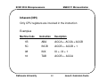
Immediate (IMM)
– The operand value is part of the instruction
– It follows the OpCode
Examples
Machine Code
Instruction
Description
86 25
LDAA #$25
ACCA ← $25
81 24
CMPA #%100100
ACCA – %00100100
CC 07 D2
LDD #!2002
ACCA:ACCB ← $07D2
Same as ACCD ← $07D2
Dalhousie University
44
Jose A. Gonzalez-Cueto
ECED 3204. Microprocessors
M68HC11 Microcontroller
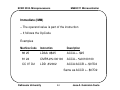
Direct (DIR)
– The operand is stored in initial 256 bytes ($0000 – $00FF)
Examples
Machine Code
Instruction
Description
90 1F
SUBA $1F
ACCA ← ACCA – <$001F>
96 A8
LDAA $A8
ACCA ← <$00A8>
Dalhousie University
45
Jose A. Gonzalez-Cueto
ECED 3204. Microprocessors
M68HC11 Microcontroller
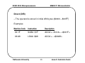
Extended (EXT)
– The operand’s absolute address appears explicitly in the
2 bytes following the OpCode (any in $0000 – $FFFF)
Examples
Machine Code Instruction
Description
B7 C0 20
STAA $C020
<$C020> ← ACCA
F0 C0 1C
SUBB $C01C
ACCB ← ACCB – <$C01C>
Dalhousie University
46
Jose A. Gonzalez-Cueto
ECED 3204. Microprocessors
M68HC11 Microcontroller
Indexed (IND)
– Index registers IX & IY are used to calculate the effective
address (EA). It can be any in $0000 – $FFFF.
– EA = Base Address + Unsigned 8-bit Offset
IX or IY
Examples
Machine Code Instruction
Description
E3 22
ADDD $22,X
EA = IX + $22
ACCD ← ACCD + <EA:EA+1>
18 AB 0D
ADDA $0D,Y
EA = IY + $0D
ACCA ← ACCA + <EA>
Dalhousie University
47
Jose A. Gonzalez-Cueto
ECED 3204. Microprocessors
M68HC11 Microcontroller
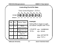
Relative (REL)
– It is used only by the branch instructions
– EA = Next Instruction’s Address + Signed 8-bit Offset, OR
PCNEW = EA = PCOLD + Offset
– Offset range: [ -128 D , 127 D ]
Dalhousie University
48
Jose A. Gonzalez-Cueto
ECED 3204. Microprocessors
M68HC11 Microcontroller
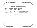
Relative (REL)
– PCNEW = EA = PCOLD + Offset
Example: Fill in the spaces in the machine code below
Address Mach Code
Label Operation Operand Description
C000
C002
C004
C006
C008
C00A
there BRA
where BHI
BCC
hang
BEQ
here
BLO
lbcc
BSR
20 __
22 __
24 __
27 __
25 __
8D __
where
there
lbcc
hang
here
subr1
branch always
branch if higher
branch if carry clear
branch if Z = 1
branch if lower
branch to subroutine
10 bytes of code
C016
4F
Dalhousie University
subr1
CLRA
49
Jose A. Gonzalez-Cueto
ECED 3204. Microprocessors
M68HC11 Microcontroller
The 68HC11 Machine Code
A 68HC11 instruction consists of
( 1 to 2 bytes ) of opcode
+
( 0 to 3 bytes ) of operand information
Examples
Machine instruction
(in hex format always)
Assembly instruction
INCB
LDAA
ADDA
5C
86 1D
9B 2F (assembler encodes using
direct addressing mode)
B7 C0 1E
1A 83 00 FF
18 1F 00 80 FB
#!29
$002F
STAA $C01E
CPD
#$00FF
loop BRCLR 0, Y, $80, loop
Dalhousie University
50
Jose A. Gonzalez-Cueto
ECED 3204. Microprocessors
M68HC11 Microcontroller
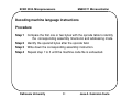
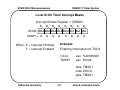
Decoding machine language instructions
Procedure
Step 1 Compare the first one or two bytes with the opcode table to identify
the corresponding assembly mnemonic and addressing mode.
Step 2 Identify the operand bytes after the opcode field.
Step 3 Write down the corresponding assembly instruction.
Step 4 Repeat step 1 to 3 until the machine code file is exhausted.
Dalhousie University
51
Jose A. Gonzalez-Cueto
ECED 3204. Microprocessors
M68HC11 Microcontroller
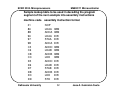
Sample lookup table to be used in decoding the program
segment of the next example into assembly instructions
machine code
01
86
8B
96
97
9B
C3
C6
CB
CC
D3
D6
D7
DB
DC
DD
Dalhousie University
assembly instruction format
NOP
LDAA
ADDA
LDAA
STAA
ADDA
ADDD
LDAB
ADDB
LDD
ADDD
LDAB
STAB
ADDB
LDD
STD
IMM
IMM
DIR
DIR
DIR
IMM
IMM
IMM
IMM
DIR
DIR
DIR
DIR
DIR
DIR
52
Jose A. Gonzalez-Cueto
ECED 3204. Microprocessors
M68HC11 Microcontroller
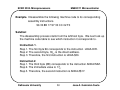
Example. Disassemble the following machine code to its corresponding
assembly instructions.
96 30 8B 17 97 30 CC 02 F0
Solution:
The disassembly process starts from the leftmost byte. We next look up
the machine code table to see which instruction it corresponds to.
Instruction 1.
Step 1. The first byte 96 corresponds to the instruction LDAA DIR.
Step 2. The second byte, 30h, is the direct address.
Step 3. Therefore, the first instruction is LDAA $30.
Instruction 2.
Step 1. The third byte (8B) corresponds to the instruction ADDA IMM.
Step 2. The immediate value is 17h.
Step 3. Therefore, the second instruction is ADDA #$17.
Dalhousie University
53
Jose A. Gonzalez-Cueto
ECED 3204. Microprocessors
M68HC11 Microcontroller
Instruction 3.
Step 1. The fifth byte (97) corresponds to the instruction STAA DIR.
Step 2. The DIR address is the next byte 30.
Step 3. Therefore, the third instruction is STAA $30.
Instruction 4.
Step 1. The seventh byte (CC) corresponds to the instruction LDD IMM.
Step 2. The IMM 16-bit value is given by the next 2 bytes 02 F0.
Step 3. Therefore, the fourth instruction is LDD #$02F0.
Dalhousie University
54
Jose A. Gonzalez-Cueto
ECED 3204. Microprocessors
Dalhousie University
M68HC11 Microcontroller
55
Jose A. Gonzalez-Cueto
ECED 3204. Microprocessors
M68HC11 Microcontroller
Assembler Line Statement Format
Label
Field
Operation Operand
Field
Field
ldab
DelayLoop
Comment
Field
# 26
; Initializing Delay Counter
decb
bne
Dalhousie University
; Decrement Counter Value
DelayLoop ; If Counter not Zero stay in the Loop
56
Jose A. Gonzalez-Cueto
ECED 3204. Microprocessors
M68HC11 Microcontroller
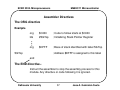
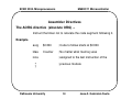
Assembler Directives
The ORG directive
Example
org
$C000
; Code to follow starts at $C000
lds
#StkTop
; Initializing Stack Pointer Register
org
$DFFF
; Base of stack identified with label StkTop
StkTop
; Address $DFFF is assigned to this label
end
The END directive.Instruct the assembler to stop the assembly process for this
module. Any directive or code following it is ignored.
Dalhousie University
57
Jose A. Gonzalez-Cueto
ECED 3204. Microprocessors
M68HC11 Microcontroller
Assembler Directives
The AORG directive (absolute ORG) .Instruct the linker not to relocate the code segment following it.
Example
aorg
$C300
; Code to follow starts at $C300
ldaa
Counter
; No matter what memory was
inca
; assigned to the last instruction of the
; previous module
Dalhousie University
58
Jose A. Gonzalez-Cueto
ECED 3204. Microprocessors
M68HC11 Microcontroller
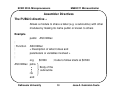
Assembler Directives
The PUBLIC directive .Allows a module to share a label (e.g. a subroutine) with other
modules by making its name public or known to others
Example
public
;
; Function
;
;
;
ASCII2Dec
ASCII2Dec
< Description of what it does and
parameters or variables involved >
org
ASCII2Dec psha
rts
$C500
; Code to follow starts at $C500
Body of the
subroutine
end
Dalhousie University
59
Jose A. Gonzalez-Cueto
ECED 3204. Microprocessors
M68HC11 Microcontroller
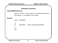
Assembler Directives
The EXTERN directive .Allows a module to have access to a public label external to
this module, i.e. not defined in this module
Example
extern ASCII2Dec
jsr
ASCII2Dec
; Call to subroutine ASCII2Dec
end
Dalhousie University
60
Jose A. Gonzalez-Cueto
ECED 3204. Microprocessors
M68HC11 Microcontroller
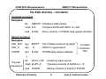
The EQU directive .- Constants
Unnamed Constants
Examples:
lds
# $DFFF ; Initializing stack pointer
cmpb # ’A’
; Compare ACCB with ASCII ‘A’ = $41
staa
; Store <ACCA> to PORTB data register ($1004)
$1004
Named Constants
Examples:
STK_TOP
equ
$DFFF ; Top of Stack at start of program
CAP_A
equ
’A’
; ASCII for uppercase A
PORTB
equ
$1004
; PORTB data register address
lds
#STK_TOP ; Initializing stack pointer
Program
Instructions
Constant
Definition
Part
cmpb #CAP_A
; Checking contents of ACCB w.r.t. ‘A’
staa
; Writing contents of ACCA to PORTB
PORTB
Dalhousie University
61
Jose A. Gonzalez-Cueto
ECED 3204. Microprocessors
M68HC11 Microcontroller
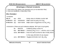
Advantages of Named Constants
1. Their value only needs to be changed once (in the Definition Part)
2. Improves readability of Assembly Code
Other Examples:
; Constants
DELAY
equ
2000
; Delay value to initialize counter with
BITMASK1 equ
%00000001 ; Mask used for parity, bit 0 (B0)
BITMASK2 equ
%00110000 ; Mask used to toggle bits 4 & 5 (B4 & B5)
; Instructions (These are just isolated examples, NOT part of a program)
ldx
#DELAY
; Initializing delay counter IX
bita
#BITMASK1 ; Checking if B0 is 0 or 1, <ACCA> even or odd
anda #BITMASK1 ; Does the same as bita but also modify ACCA
; In this case ACCA B1-B7 are cleared
eora #BITMASK2 ; Toggles ACCA bits 4 & 5 (B4 & B5)
Dalhousie University
62
Jose A. Gonzalez-Cueto
ECED 3204. Microprocessors
M68HC11 Microcontroller
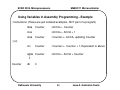
Using Variables in Assembly Programming.- Example
; Instructions (These are just isolated examples, NOT part of a program)
ldaa
Counter
inca
; ACCA ← Counter
; ACCA ← ACCA + 1
staa
Counter
; Counter ← ACCA, updating Counter
inc
Counter
; Counter ← Counter + 1, Equivalent to above
; (or)
adda Counter
Counter
db
; ACCA ← ACCA + Counter
0
Dalhousie University
63
Jose A. Gonzalez-Cueto
ECED 3204. Microprocessors
M68HC11 Microcontroller
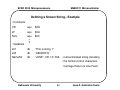
Defining a Known String.- Example
; Constants
CR
equ
$0D
LF
equ
$0A
NUL
equ
$00
str1
db
“This is string 1”
str3
db
“ABCDEFG”
NameStr
db
“JOSE”, CR, LF, NUL ; null-terminated string including
; Variables
; the format control characters
; Carriage Return & Line Feed
Dalhousie University
64
Jose A. Gonzalez-Cueto
ECED 3204. Microprocessors
M68HC11 Microcontroller
Reserving arbitrary amounts of storage .- Example
; Program segment that stores string “ABC…Z” to variable alphabet
; Constants
CAP_A
equ
‘A’
; First letter, ‘A’ has the lowest ASCII value in the set
CAP_Z
equ
‘Z’
; Last letter, ‘Z’ has the highest ASCII value in the set
; Instructions
org
ldx
ldaa
AlphaLoop staa
inx
inca
cmpa
bls
$C000
#alphabet
#CAP_A
0,X
; Code below to be loaded starting at $C000
; IX pointing to alphabet (loaded with its address)
; ACCA = ‘A’
; Store value in ACCA to address held by IX
; Increment IX, IX points to next byte in alphabet
; ACCA holds ASCII value for next character
#CAP_Z ; Is next char lower or same as ‘Z’ ?
AlphaLoop ; If YES go back to store it and repeat cycle
; Variables
alphabet
ds
26
Dalhousie University
; Allocates 26 bytes of memory for variable
; alphabet . Its values are undefined initially.
65
Jose A. Gonzalez-Cueto
ECED 3204. Microprocessors
M68HC11 Microcontroller
Reserving arbitrary storage .- List File Example
1: ; Program segment that stores string "ABC...Z" to variable alphabet
2:
3: ; Constants
4:
=00000041
CAP_A
equ 'A'
5:
=0000005A
CAP_Z
equ 'Z'
6:
7: ; Instructions
8:
=0000C000
org $C000
9: C000 CE C00D
ldx
#alphabet
10: C003 86 41
ldaa #CAP_A
11: C005 A7 00AlphaLoop staa 0,X
12: C007 08
inx
13: C008 4C
inca
14: C009 81 5A
cmpa #CAP_Z
15: C00B 23 F8
bls
AlphaLoop
16:
17: ; Variables
18: C00D +001A
alphabet
ds
!26
Dalhousie University
66
Jose A. Gonzalez-Cueto
ECED 3204. Microprocessors
M68HC11 Microcontroller
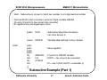
;
; HtoD - Subroutine to convert a 16-bit hex number to a 5 digit decimal number
;
; Decimal ASCII result is stored in external 5 byte variable DBUFR
; On entry IX points to hex value to be converted
; All registers are unchanged upon return
;
HtoD
public
HtoD
; Subroutine label other module(s)
; can have access to
extern
DBUFR
; Variable label defined in other module
pshy
pshx
pshb
psha
ldy
ldd
ldx
idiv
; Save registers
#DBUFR
0,X
#!10000
; IY points to DBUFR variable
; ACCD = hex value to be converted
; IX = hex/10,000, ACCD = remainder (r)
Subroutine Example (Part 1)
Dalhousie University
67
Jose A. Gonzalez-Cueto
ECED 3204. Microprocessors
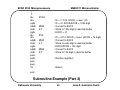
ldx
idiv
xgdx
addb
stab
xgdx
ldx
idiv
addb
stab
xgdx
addb
stab
pula
pulb
pulx
puly
rts
M68HC11 Microcontroller
#!100
#$30
2,Y
; IX = r1/100, ACCD = new r (r2)
; IX = r2, ACCA:ACCB = 100s digit
; Convert to ASCII
; Store to 100s digit in decimal buffer
; ACCD = r2
#!10
#$30
4,Y
#$30
3,Y
; IX = r2/10, ACCD = new r (ACCB = 1s digit)
; Convert to ASCII
; Store to units digit in decimal buffer
; ACCA:ACCB = 10s digit
; Convert to ASCII
; Store to 10s digit in decimal buffer
; Restore registers
; Return
end
Subroutine Example (Part 2)
Dalhousie University
68
Jose A. Gonzalez-Cueto
ECED 3204. Microprocessors
M68HC11 Microcontroller
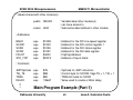
; Labels shared with other module(s)
public
DBUFR
; Variable label other module(s)
; can have access to
extern HtoD
; Subroutine label defined in other module
equ
equ
equ
equ
equ
equ
$102B
$102C
$102E
$102F
$4000
$DFFF
; Address for the SCI line speed register
; Address for the SCI control register 1
; Address for the SCI status register
; Address for the SCI data register
; FlipFlop Address
; Address of top-of-stack
equ
equ
equ
equ
$7E
$88
$80
!10667
; OpCode for JMP instruction
; Control byte for SCCR2, flags TE = 1, TIE = 1
; TDRE bit mask for SCSR
; Value used to create a 32ms delay,
; Addresses
BAUD
SCCR1
SCSR
SCDR
FFLOP
STK_TOP
; Constants
JMPOpCode
TIE_TE
TDRE
DELAY
Main Program Example (Part 1)
Dalhousie University
69
Jose A. Gonzalez-Cueto
ECED 3204. Microprocessors
M68HC11 Microcontroller
; Program Code
MainLoop
DelayLoop
org
$C000
; To be loaded at $C000
lds
ldx
dex
bne
jsr
bra
#STK_TOP
#DELAY
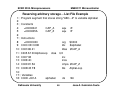
DelayLoop
UpdatePeriod
MainLoop
; Initializing stack pointer
; Loading delay counter
; Decrementing counter
; If counter > 0 keep decrementing
; Goto Update Signal Period
; Repeat Loop
ldx
jsr
ldx
#Periodhex
HtoD
#DBUFR
; Load IX with address of hex period
; Subroutine call
; Reading subroutine output
UpdatePeriod
rts
NewLineString
DBUFR
Periodhexdw
db
ds
0
; End of subroutine UpdatePeriod
LF, CR, ' ', NUL
5
end
Variables (Part of them)
; End of Program Code
Main Program Example (Part 2)
Dalhousie University
70
Jose A. Gonzalez-Cueto
ECED 3204. Microprocessors
M68HC11 Microcontroller
M68HC11 Instruction Set & Assembly Programming
Bibliography:
• 68HC11 Reference Manual, Section 6.5 and Appendix A.
• 68HC11 Programming Reference Guide, Section 3.
• Textbook, Chapter 3.
• Huang’s book, Chapter 2.
Dalhousie University
71
Jose A. Gonzalez-Cueto
ECED 3204. Microprocessors
M68HC11 Microcontroller
M68HC11 Instruction Set
Load & Store Instructions .- Examples
ldaa
#$2C
; ACCA ← $2C
ldab
$C007 ; ACCB ← <$C007>
staa
$C00A ; <$C00A> ← ACCA
Register Transfer & Exchange Instructions
tab
; ACCB ← ACCA
tba
; ACCA ← ACCB
xgdx ; ACCD ↔ IX
xgdy ; ACCD ↔ IY
Dalhousie University
72
Jose A. Gonzalez-Cueto
ECED 3204. Microprocessors
M68HC11 Microcontroller
M68HC11 Instruction Set
Arithmetic Instructions .- Examples
inc
Counter ; Counter ← Counter + 1
deca
; ACCA ← ACCA – 1
adda alpha
; ACCA ← ACCA + alpha
suba beta
; ACCA ← ACCA – beta
aba
; ACCA ← ACCA + ACCB
nega
; ACCA ← – ACCA (2’s complement)
mul
; ACCD ← ACCA ∗ ACCB
Dalhousie University
73
Jose A. Gonzalez-Cueto
ECED 3204. Microprocessors
M68HC11 Microcontroller
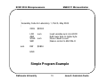
;
; Assembly Code for Laboratory 1, Part 5, May 2003
;
ORG $D000
sum
LDD
ABA
STAA
SWI
sum
DW
$0804
sum
; Load variable sum into ACCD
; Add lower byte to higher byte
; Store it back to sum
; Return control to BUFFALO
END
Simple Program Example
Dalhousie University
74
Jose A. Gonzalez-Cueto
ECED 3204. Microprocessors
M68HC11 Microcontroller
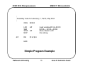
;
; Assembly Code for Laboratory 1, Part 5, May 2004
;
ORG $C500
diff
LDD
SBA
STAA
NOP
diff
DB
$1E, $04
diff
; Load variable diff into ACCD
; ACCA ← ACCA – ACCB
; Store it back to diff
; Do nothing
END
Simple Program Example
Dalhousie University
75
Jose A. Gonzalez-Cueto
ECED 3204. Microprocessors
M68HC11 Microcontroller
M68HC11 Instruction Set
Logical Operations .- Examples
andb #$F0
; Clears Least Significant Nibble of ACCB
oraa #$03
; Sets Bits 0 & 1 of ACCA
eora #$0C
; Toggles Bits 2 & 3 of ACCA
bitb
$C01C
; Implicit AND, ACCB • <$C01C>
; Flags modified, ACCB not altered
bitb
#%00000011 ; Is ACCB multiple of 4?
; If as a result of this instruction Z is set
; (Z = 1), ACCB is multiple of 4.
ldx
bset
bclr
#$1004
0, X, $55
0, X, $AA
Dalhousie University
; Sets bits 0,2,4 & 6 of PORTB
; Clears bits 1,3,5,7 of PORTB
76
Jose A. Gonzalez-Cueto
ECED 3204. Microprocessors
M68HC11 Microcontroller
M68HC11 Instruction Set
Shift and Rotate Instructions
Dalhousie University
77
Jose A. Gonzalez-Cueto
ECED 3204. Microprocessors
M68HC11 Microcontroller
M68HC11 Instruction Set
Shift and Rotate Instructions .- Examples
ldaa
#$01 ;
ACCA = 1 = 00000001bin
asla
; ACCA = ACCA ∗ 2 = 2 = 00000010bin, Carry flag = 0
asla
; ACCA = ACCA ∗ 2 = 4 = 00000100bin, Carry flag = 0
asra
; ACCA = ACCA / 2 = 2 = 00000010bin, Carry flag = 0
ldaa
asra
#$F6 ;
ACCA = -10dec = $F6 = 11110110bin
; ACCA = ACCA / 2 = -5dec = $FB = 11111011bin,
; Carry Flag = 0
asra
; ACCA = ACCA / 2 = -3dec = $FD = 11111101bin,
; Carry Flag = 1
Dalhousie University
78
Jose A. Gonzalez-Cueto
ECED 3204. Microprocessors
M68HC11 Microcontroller
M68HC11 Instruction Set
Program Control Instructions
1. Conditional branches
• Modify value of PC within [-128,+127]dec (1 byte signed)
(a) Testing a single CCR bit
beq
<label>
;Z=1?
bne
<label>
;Z=0?
bcs
<label>
;C=1?
bcc
<label>
;C=0?
Dalhousie University
79
Jose A. Gonzalez-Cueto
ECED 3204. Microprocessors
M68HC11 Microcontroller
M68HC11 Instruction Set
Program Control Instructions
1. Conditional branches
(b) Comparison of unsigned numbers
bhi
bhs
blo
bls
<label>
<label>
<label>
<label>
; Unsigned > ,
; Unsigned ≥ ,
; Unsigned < ,
; Unsigned ≤ ,
C+Z=0?
C=0?
C=1?
C+Z=1?
Example:
cmpa #$25
bhi
Higher ; Program control will be transferred to the
; instruction at label ‘Higher’ IF ACCA > $25,
; otherwise the instruction following bhi is
; executed
; If ACCA = $F3 = 243dec > $25 execution
; continues at ‘Higher’
Dalhousie University
80
Jose A. Gonzalez-Cueto
ECED 3204. Microprocessors
M68HC11 Microcontroller
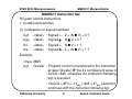
M68HC11 Instruction Set
Program Control Instructions
1. Conditional branches
(c) Comparison of signed numbers
bgt
bge
blt
ble
<label>
<label>
<label>
<label>
; Signed > ,
; Signed ≥ ,
; Signed < ,
; Signed ≤ ,
Z + (N ⊕ V) = 0 ?
N⊕V=0?
N⊕V=1?
Z + (N ⊕ V) = 1 ?
Example:
cmpa #$25
bgt
Greater ; Program control is transferred to the instruction
; at label ‘Greater’ IF the 2’s complement value in
; ACCA > $25, otherwise the instruction following
; bgt is executed
; If ACCA = $F3 = -13dec < $25 = 37dec execution
; continues with the instruction following bgt
Dalhousie University
81
Jose A. Gonzalez-Cueto
ECED 3204. Microprocessors
M68HC11 Microcontroller
M68HC11 Instruction Set
Program Control Instructions
2. Unconditional branches
jmp <label or address>
; Jump always to a label / address
; in the 64KB address space
bra <label> ; Branch always to an address in the range
; [ PC - 128dec , PC + 127dec ]
3. Subroutine calls
jsr
<label or address> ; Jump to a subroutine starting with
; a label / address anywhere in the
; 64KB address space
bsr
<label> ; Branch to a subroutine starting with a label
; associated with an address in the range
; [ PC - 128dec , PC + 127dec ],
; PC is the address of the instruction following bsr
rts
Dalhousie University
; Return from subroutine
82
Jose A. Gonzalez-Cueto
ECED 3204. Microprocessors
M68HC11 Microcontroller
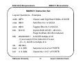
M68HC11 Instruction Set
Stack Instructions
1. Saving contents of CPU registers
psha
pshb
pshx
pshy
; Storing register values to stack
2. Retrieving contents of CPU registers
puly
pulx
pulb
pula
Dalhousie University
; Restoring register values from stack
83
Jose A. Gonzalez-Cueto
ECED 3204. Microprocessors
M68HC11 Microcontroller
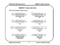
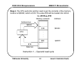
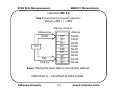
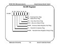
Internal
CPU Registers
Description
BAR
Bus Address Register – 16 bits
BDR
Bus Data Register – 8 bits
IR
Instruction Register – 8 bits
ATMP
Temporal Address Register – 16 bits
DTMP
Temporal Data Register – 16 bits
Dalhousie University
84
Jose A. Gonzalez-Cueto
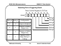
ECED 3204. Microprocessors
M68HC11 Microcontroller
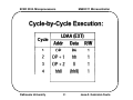
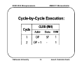
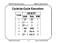
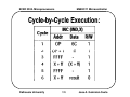
Cycle Code
Description
FOP
Fetch instruction Opcode
FOFF
Fetch 8-bit address Offset
FAHI
Fetch High half of 16-bit Address
FALO
Fetch Low half of 16-bit Address
ODHI
transfer High half of 16-bit Operand Data
ODLO
transfer Low half of 16-bit Operand Data
OD
transfer 8-bit Operand Data
CA
Compute operand Address (uses ALU)
EXEC
execute ("do" the instruction)
Dalhousie University
85
Jose A. Gonzalez-Cueto
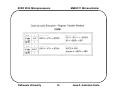
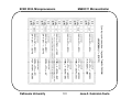
; Assembly code for Cycle-by
by-Cycle Execution example
$C000
; Instruction execution is analyzed for
THIS,
org
THIS,
THIS instruction
;
;
Target
;
THIS, and
Data
jsr
$C080
clrb
org
2,X
$D400
2
$39
inc
org
ds
db
$D500
#STK_TOP
#List
#$5F
Code
$D000
$19
org
lds
ldx
ldab
jmp
$DFFF
org
db
org
;
ldaa
; Execution starts at $D500 (Reset vector is set to $D500)
; Instructions
; ************
Code
Target
; Data
; ****
Data
List
; Initialization
; **************
; Stack Area
; ***** ****
STK_TOP
end
Jose A. Gonzalez-Cueto
86
Dalhousie University
M68HC11 Microcontroller
ECED 3204. Microprocessors
ECED 3204. Microprocessors
M68HC11 Microcontroller
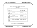
The 68HC11 Instruction Execution Cycle
-
Perform a sequence of read cycles to fetch instruction opcode byte(s)
and address byte(s) if required.
Optionally perform read cycle(s) required to fetch memory operand(s).
Perform the operation specified by the opcode.
Optionally write results back to a register or memory location(s).
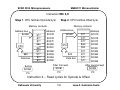
Example: Consider the following 4 instructions
Assembly instruction
Memory location
Machine Code
LDAA $D000
CLRB
JSR
$C080
$C000
$C003
$C004
B6 D0 00
5F
BD C0 80
INC
2,X
$C080
6C 02
Dalhousie University
87
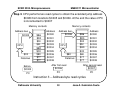
Jose A. Gonzalez-Cueto
ECED 3204. Microprocessors
M68HC11 Microcontroller
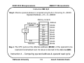
Instruction LDAA $D000
Step 1. Place the value in PC on the address bus with a request to read the
contents of that location.
Step 2. The opcode byte $B6 at $C000 is returned to the CPU and PC is
incremented by 1.
Memory contents
Address
Address bus
$C000
$B6
$D0
$00
$5F
$BD
$C0
$80
$??
$??
CPU
$B6
Data bus
Before
$C000
PC
$C000
$C001
$C002
$C003
$C004
$C005
$C006
$C007
$C008
After
$C001
PC
Instruction 1 -- Opcode read cycle
Dalhousie University
88
Jose A. Gonzalez-Cueto
ECED 3204. Microprocessors
M68HC11 Microcontroller
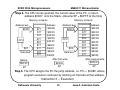
Step 3. CPU performs two read cycles to obtain the extended address
$D000 from locations $C001 and $C002. At the end the value of PC is
incremented to $C003
Memory contents
Memory contents
Address bus
$C001
CPU
$D0
Data bus
$B6
$D0
$00
$5F
$BD
$C0
$80
$??
$??
Before
$C001
PC
Address bus
Address
$C000
$C001
$C002
$C003
$C004
$C005
$C006
$C007
$C008
$C002
CPU
$00
Data bus
After first read
$C002
PC
$B6
$D0
$00
$5F
$BD
$C0
$80
$??
$??
Address
$C000
$C001
$C002
$C003
$C004
$C005
$C006
$C007
$C008
After second read
$C003
PC
Instruction 1 -- Read cycles for address bytes
Dalhousie University
89
Jose A. Gonzalez-Cueto
ECED 3204. Microprocessors
M68HC11 Microcontroller
Step 4. The CPU performs another read to get the contents of the memory
location at $D000, which is $19. The value $19 will be loaded into ACCA.
i.e. ACCA ← $19
Memory contents
Address
$19
$D000
Address bus
$D000
.
.
.
CPU
$00
$DFFF
$19
Data bus
Instruction 1 -- Operand read cycle
Dalhousie University
90
Jose A. Gonzalez-Cueto
ECED 3204. Microprocessors
Dalhousie University
M68HC11 Microcontroller
91
Jose A. Gonzalez-Cueto
ECED 3204. Microprocessors
Dalhousie University
M68HC11 Microcontroller
92
Jose A. Gonzalez-Cueto
ECED 3204. Microprocessors
M68HC11 Microcontroller
Instruction CLRB
Step 1. Place the value in PC on the address bus with a request to read the
contents of that location.
Step 2. The opcode byte $5F at $C003 is returned to the CPU and PC is
incremented by 1.
Memory contents
Address
Address bus
$C003
$B6
$D0
$00
$5F
$BD
$C0
$80
$??
$??
CPU
$5F
Data bus
Before
$C003
PC
$C000
$C001
$C002
$C003
$C004
$C005
$C006
$C007
$C008
After
$C004
PC
Instruction 2 -- Opcode read cycle
Dalhousie University
93
Jose A. Gonzalez-Cueto
ECED 3204. Microprocessors
M68HC11 Microcontroller
Instruction 2, CLRB -- Execution
Step 3. Once decoded the corresponding action is taken, i.e. ACCB ← 0.
No operands are read in this Instruction, just a single OpCode byte.
Neither any memory location is written as result of the operation.
Dalhousie University
94
Jose A. Gonzalez-Cueto
ECED 3204. Microprocessors
Dalhousie University
M68HC11 Microcontroller
95
Jose A. Gonzalez-Cueto
ECED 3204. Microprocessors
Dalhousie University
M68HC11 Microcontroller
96
Jose A. Gonzalez-Cueto
ECED 3204. Microprocessors
M68HC11 Microcontroller
Instruction JSR $C080
Step 1. Place the value in PC on the address bus with a request to read the
contents of that location.
Step 2. The opcode byte $BD at $C004 is returned to the CPU and PC is
incremented by 1.
Memory contents
Address
Address bus
$C004
$B6
$D0
$00
$5F
$BD
$C0
$80
$??
$??
CPU
$BD
Data bus
Before
$C004
PC
$C000
$C001
$C002
$C003
$C004
$C005
$C006
$C007
$C008
After
$C005
PC
Instruction 3 -- Opcode read cycle
Dalhousie University
97
Jose A. Gonzalez-Cueto
ECED 3204. Microprocessors
M68HC11 Microcontroller
Step 3. CPU performs two read cycles to obtain the extended jump address
$C080 from locations $C005 and $C006. At the end the value of PC
is incremented to $C007
Memory contents
Memory contents
Address bus
$C005
CPU
$C0
Data bus
$B6
$D0
$00
$5F
$BD
$C0
$80
$??
$??
Address
$C000
$C001
$C002
$C003
$C004
$C005
$C006
$C007
$C008
Address bus
$C006
CPU
$80
Data bus
After first read
$C006
PC
Before
$C005
PC
$B6
$D0
$00
$5F
$BD
$C0
$80
$??
$??
Address
$C000
$C001
$C002
$C003
$C004
$C005
$C006
$C007
$C008
After second read
$C007
PC
Instruction 3 -- Address byte read cycles
Dalhousie University
98
Jose A. Gonzalez-Cueto
ECED 3204. Microprocessors
M68HC11 Microcontroller
Step 4. The CPU stores (pushes) the current value of the PC, or return
address $C007, onto the Stack. (Assume SP = $DFFF at the time)
Memory contents
Memory contents
Address bus
$DFFF
CPU
$07
Data bus
$??
$??
$??
$??
$07
$??
$??
$??
$??
Before
$DFFF
SP
Address bus
Address
$DFFB
$DFFC
$DFFD
$DFFE
$DFFF
$E000
$E001
$E002
$E003
$DFFE
CPU
$C0
Data bus
$??
$??
$??
$C0
$07
$??
$??
$??
$??
Address
$DFFB
$DFFC
$DFFD
$DFFE
$DFFF
$E000
$E001
$E002
$E003
After second write
$DFFD
SP
After first write
$DFFE
SP
Step 5. The CPU assigns the PC the jump address, i.e. PC ← $C080, where
program execution continues by fetching an OpCode at that address.
Instruction 3 -- Execution
Dalhousie University
99
Jose A. Gonzalez-Cueto
ECED 3204. Microprocessors
Dalhousie University
M68HC11 Microcontroller
100
Jose A. Gonzalez-Cueto
ECED 3204. Microprocessors
Dalhousie University
M68HC11 Microcontroller
101
Jose A. Gonzalez-Cueto
ECED 3204. Microprocessors
M68HC11 Microcontroller
Instruction INC 2,X
Step 1. CPU fetches OpCode byte
Step 2. CPU fetches offset byte
Memory contents
Memory contents
Address bus
$C080
CPU
$6C
Data bus
$??
$??
$??
$6C
$02
$??
$??
$??
$??
Before
$C080
PC
Address
$C07D
$C07E
$C07F
$C080
$C081
$C082
$C083
$C084
$C085
Address bus
$C081
CPU
$02
Data bus
After first read
$C081
PC
$??
$??
$??
$6C
$02
$??
$??
$??
$??
Address
$C07D
$C07E
$C07F
$C080
$C081
$C082
$C083
$C084
$C085
After second read
$C082
PC
Instruction 4 -- Read cycles for Opcode & Offset
Dalhousie University
102
Jose A. Gonzalez-Cueto
ECED 3204. Microprocessors
M68HC11 Microcontroller
Instruction INC 2,X
Step 3. Effective operand address is computed using the ALU. Assuming IX = $D400:
Operand Address = IX + 2 = $D402
Memory contents
Address bus
$D402
CPU
$39
Data bus
Address
$??
$??
$??
$??
$39
$??
$??
$??
$??
$D3FE
$D3FF
$D400
$D401
$D402
$D403
$D404
$D405
$D406
Step 4. The CPU puts out the effective address ($D402) of the operand to be
read and incremented next. Its value is returned in the data bus($39)
Instruction 4 -- Computing operand address & operand read cycle
Dalhousie University
103
Jose A. Gonzalez-Cueto
ECED 3204. Microprocessors
M68HC11 Microcontroller
Instruction INC 2,X
Step 5. Executing the increment operation:
Result = $39 + 1 = $3A
Memory contents
Address bus
$D402
CPU
$3A
Data bus
Address
$??
$??
$??
$??
$3A
$??
$??
$??
$??
$D3FE
$D3FF
$D400
$D401
$D402
$D403
$D404
$D405
$D406
Step 6. Storing the result back to the memory address
Instruction 4 -- Increment & write cycles
Dalhousie University
104
Jose A. Gonzalez-Cueto
ECED 3204. Microprocessors
Dalhousie University
M68HC11 Microcontroller
105
Jose A. Gonzalez-Cueto
ECED 3204. Microprocessors
Dalhousie University
M68HC11 Microcontroller
106
Jose A. Gonzalez-Cueto
ECED 3204. Microprocessors
Dalhousie University
M68HC11 Microcontroller
107
Jose A. Gonzalez-Cueto
ECED 3204. Microprocessors
M68HC11 Microcontroller
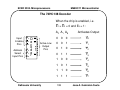
The 74HC138 Decoder
When the chip is enabled, i.e.
E1 = E2 = 0 and E3 = 1:
A2 A1 A0
Input
Enable
Pins
E3
Address
Select
Input Pins
A2
A1
E1
E2
A0
D Y0
e Y1
c
o
d
e Y7
r
Active-Low
Output
Pins
Dalhousie University
Activates Output
0
0
0
Y0
0
0
1
Y1
0
1
0
Y2
0
1
1
Y3
1
0
0
Y4
1
0
1
Y5
1
1 0
Y6
1
1
Y7
108
1
Jose A. Gonzalez-Cueto
ECED 3204. Microprocessors
M68HC11 Microcontroller
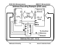
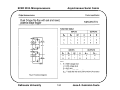
Address Decoding Example (EVB case)
A0
A1
D0
D1
CPU D7
A12
A13
R/W
A15
E-Clk
Data
Bus
(D0 - D7)
Memory
D0 Module
D1
D7
W
A0
A1
8K x 8
RAM A12
OE (G)
E3
E1
E2
A2
A1
A0
D
e
c
o
d
e Y7
r
Y0
Y1
CS (E1)
To Another
Memory
Module
CS
Address Bus (A0 - A12)
Dalhousie University
109
Jose A. Gonzalez-Cueto
ECED 3204. Microprocessors
M68HC11 Microcontroller
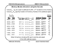
Memory Module Allocation using the Decoder
• Lines A12 - A0 are used to address the 8K = 213 locations in the module
• Lines A15-A13 specify location of memory module in the address space
A15-A12
Min – Max
0000 – 0001
0010 – 0011
0100 – 0101
0110 – 0111
1000 – 1001
1010 – 1011
1100 – 1101
1110 – 1111
Active
A15 14 13 12
00
00
01
01
10
10
11
11
0x
1x
0x
1x
0x
1x
0x
1x
11 10 9 8
x
x
x
x
x
x
x
x
xxx
xxx
xxx
xxx
xxx
xxx
xxx
xxx
1 0
Address Range
Pin
xx
xx
xx
xx
xx
xx
xx
xx
$0000 – $1FFF
$2000 – $3FFF
$4000 – $5FFF
$6000 – $7FFF
$8000 – $9FFF
$A000 – $BFFF
$C000 – $DFFF
$E000 – $FFFF
Y0
Y1
Y2
Y3
Y4
Y5
Y6
Y7
Note: 8 memory modules 8K each could be allocated
in the 64K address space
Dalhousie University
110
Jose A. Gonzalez-Cueto
ECED 3204. Microprocessors
Dalhousie University
M68HC11 Microcontroller
111
Jose A. Gonzalez-Cueto
ECED 3204. Microprocessors
Dalhousie University
M68HC11 Microcontroller
112
Jose A. Gonzalez-Cueto
ECED 3204. Microprocessors
Dalhousie University
M68HC11 Microcontroller
113
Jose A. Gonzalez-Cueto
ECED 3204. Microprocessors
M68HC11 Microcontroller
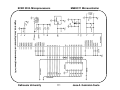
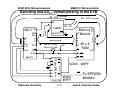
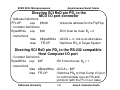
Decoding and AD0-7 Demultiplexing in the EVB
A8 - A12
A0 - A12
LE
MCU
AS
AD0
AD1
A0 - A7
Latch
OE
74HC373
A8
Memory A0
A1
D0 Module
D
1
A12
A13
AD7
A15
R/W
E-Clk
68HC11
Switch Closes
when E is High
D7
W
8K x 8
RAM
A12
G (OE)
E3
E1
E2
A2
A1
A0
E1 (CS)
D Y0
e Y1
$C000 - $DFFF
c
o
d
CS
e Y7
To EPROM
r
$E000 Module
74HC138
Dalhousie University
+5V
114
$FFFF
Jose A. Gonzalez-Cueto
ECED 3204. Microprocessors
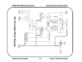
M68HC11 Microcontroller
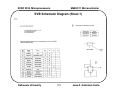
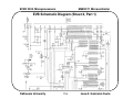
EVB Schematic Diagram (Sheet 1)
Dalhousie University
115
Jose A. Gonzalez-Cueto
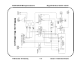
ECED 3204. Microprocessors
M68HC11 Microcontroller
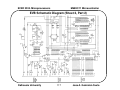
EVB Schematic Diagram (Sheet 2, Part 1)
Dalhousie University
116
Jose A. Gonzalez-Cueto
ECED 3204. Microprocessors
M68HC11 Microcontroller
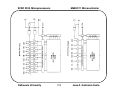
EVB Schematic Diagram (Sheet 2, Part 2)
Dalhousie University
117
Jose A. Gonzalez-Cueto
ECED 3204. Microprocessors
Dalhousie University
M68HC11 Microcontroller
118
Jose A. Gonzalez-Cueto
ECED 3204. Microprocessors
Dalhousie University
M68HC11 Microcontroller
119
Jose A. Gonzalez-Cueto
ECED 3204. Microprocessors
Dalhousie University
M68HC11 Microcontroller
120
Jose A. Gonzalez-Cueto
ECED 3204. Microprocessors
Dalhousie University
M68HC11 Microcontroller
121
Jose A. Gonzalez-Cueto
ECED 3204. Microprocessors
M68HC11 Microcontroller
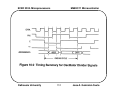
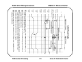
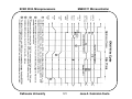
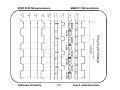
Drawing a Timing Diagram
1. Identify the Cycle Type
a) EPROM Read,
b) RAM Read, OR
c) RAM Write.
2. Find the Chip driving the AD7-0 lines
a) Address phase : HC11,
b) Data phase : HC11, EPROM OR RAM.
3. Include hex values for each bus
i.e. • A15 – A8 ,
• AD7 – AD0 , AND
• The 373 Latch Output (A7 – A0).
Dalhousie University
122
Jose A. Gonzalez-Cueto
ECED 3204. Microprocessors
Dalhousie University
M68HC11 Microcontroller
123
Jose A. Gonzalez-Cueto
ECED 3204. Microprocessors
Dalhousie University
M68HC11 Microcontroller
124
Jose A. Gonzalez-Cueto
ECED 3204. Microprocessors
Dalhousie University
M68HC11 Microcontroller
125
Jose A. Gonzalez-Cueto
ECED 3204. Microprocessors
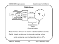
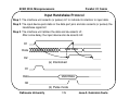
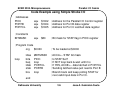
Asynchronous Serial Comm
Definitions
Clock
CPU
Data
Bus
Address Lines
UART
(Async
Serial
I/O)
TxD line
?
RxD line
Asynchronous
Serial
Communication
• Asynchronous: There is no clock to establish a time reference
• Serial: Data is carried over the channel one bit at a time,
not in parallel as over the Data Bus with the CPU
Dalhousie University
126
Jose A. Gonzalez-Cueto
ECED 3204. Microprocessors
Asynchronous Serial Comm
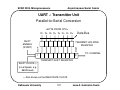
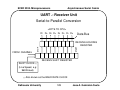
UART .- Transmitter Unit
Parallel-to-Serial Conversion
<BYTE FROM CPU>
D7 D6 D5 D4 D3 D2 D1 D0
START
TRANSMIT HOLDING
REGISTER
STOP
SHIFT
ENABLE
(START)
Data Bus
1
0
TO CHANNEL
TRANSMIT SHIFT REGISTER
SHIFT CLOCK (∗)
(Line Speed, e.g.
9600 baud)
(∗)
Also known as the BAUD RATE CLOCK
Dalhousie University
127
Jose A. Gonzalez-Cueto
ECED 3204. Microprocessors
Asynchronous Serial Comm
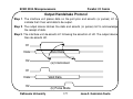
UART .- Receiver Unit
Serial-to-Parallel Conversion
<BYTE TO CPU>
D7 D6 D5 D4 D3 D2 D1 D0
Data Bus
STOP
FROM CHANNEL
START
RECEIVE HOLDING
REGISTER
RECEIVE SHIFT REGISTER
SHIFT CLOCK (∗)
(Line Speed, e.g.
9600 baud)
(∗)
Also known as the BAUD RATE CLOCK
Dalhousie University
128
Jose A. Gonzalez-Cueto
ECED 3204. Microprocessors
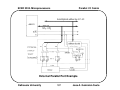
Asynchronous Serial Comm
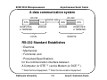
A data communication system
RS-232
RS-232
Comm Link
DTE
DCE
DCE
DTE
COMPUTER
or TERMINAL
MODEM
MODEM
COMPUTER
or TERMINAL
REMOTE
LOCAL
RS-232 Standard Establishes
• Electrical,
• Mechanical,
• Functional, and
• Procedural Specifications
for the communication interface between
A Computer (or DTE (1) ) and a Modem (or DCE (2) ).
(1) Data
Terminal Equipment, (2) Data Communication Equipment
Dalhousie University
129
Jose A. Gonzalez-Cueto
ECED 3204. Microprocessors
Asynchronous Serial Comm
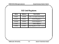
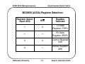
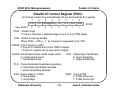
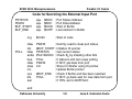
SCI Unit Registers
Name
Address
Description
BAUD
$102B
Sets Line Speed (Baud Rate)
SCCR1
$102C
Control Register 1
SCCR2
$102D
Control Register 2
SCSR
$102E
Status Register
SCDR
$102F
Data Register (for both rx & tx)
Dalhousie University
130
Jose A. Gonzalez-Cueto
ECED 3204. Microprocessors
Asynchronous Serial Comm
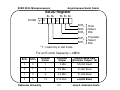
BAUD Register
B5 B4
$102B
T∗ 0
B2 B1 B0
T∗
SCR0
SCR1
SCR2
Rate
Select
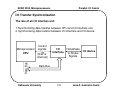
Bits
SCP0
Prescaler
Select
Bits
SCP1
∗ T - Used only in test mode
For an E-clock frequency = 2MHz
SCP1
SCP0
Division
Factor
0
0
1
2 MHz
125,000 Baud
0
1
3
2/3 MHz
41,667 Baud
1
0
4
0.5 MHz
31,250 Baud
1
1
13
2/13 MHz
≈ 9,600 Baud
Dalhousie University
Prescaler
Output
131
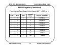
Highest Baud Rate
(Prescaler Output / 16)
Jose A. Gonzalez-Cueto
ECED 3204. Microprocessors
Asynchronous Serial Comm
BAUD Register (Continued)
For a Highest Baud Rate of 9,600 Baud (SCP1 = SCP0 = 1)
SCR2
SCR1
SCR0
Division
Factor
Selected Baud Rate
0
0
0
1
9,600 Baud
0
0
1
2
4,800 Baud
0
1
0
4
2,400 Baud
0
1
1
8
1,200 Baud
1
0
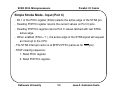
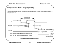
0
16
600 Baud
1
0
1
32
300 Baud
1
1
0
64
150 Baud
1
1
1
128
75 Baud
Dalhousie University
132
Jose A. Gonzalez-Cueto
ECED 3204. Microprocessors
Asynchronous Serial Comm
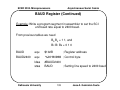
BAUD Register (Continued)
Example: Write a program segment in assembler to set the SCI
unit baud rate equal to 2400 baud.
From previous tables we need
B5 B4 = 1 1, and
B2 B1 B0 = 0 1 0
BAUD
equ
$102B
BAUD2400
equ
%00110010 ; Control byte
ldaa
staa
#BAUD2400
BAUD
; Setting line speed to 2400 baud
Dalhousie University
; Register address
133
Jose A. Gonzalez-Cueto
ECED 3204. Microprocessors
Asynchronous Serial Comm
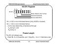
SCCR1 Register
B7 B6
B4
$102C R8 T8 0 M Wk 0
0 0
Mode (Selects char format)
Transmit Data Bit 8
Receive Data Bit 8
• M = 0, SCI rx & tx 8-bit data frames (Only SCDR is needed)
• M = 1, SCI rx & tx 9-bit data frames
– In this case data bit B8 is transferred through
. T8 during tx, and
. R8 during rx.
Frame Length
The SCI unit always uses
• 1 Start Bit, 8 or 9 Data Bits, and 1 Stop Bit = 10 or 11 bits/frame total
Dalhousie University
134
Jose A. Gonzalez-Cueto
ECED 3204. Microprocessors
Asynchronous Serial Comm
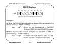
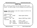
SCDR Register
B7
$102F
R7
T7
B6
R6
B5
T6
R5
T5
B4
R4
T4
B3
R3
T3
B2
R2
T2
B1
R1
T1
B0
R0
T0
(Receive and transmit double buffered)
Examples:
A) When the SCI unit has received new data and it is available for the
CPU to read it (i.e., RDRF condition)
ldaa
$102F
; Brings the new data byte held by the SCDR
; Rx buffer (RDR) into the CPU ACCA register
B) When the SCI unit is ready to accept a new byte from the CPU for
transmission (i.e., TDRE condition)
staa
$102F
Dalhousie University
; Sends the data byte in ACCA to the SCI unit
; SCDR Tx buffer (TDR) for transmission
135
Jose A. Gonzalez-Cueto
ECED 3204. Microprocessors
Asynchronous Serial Comm
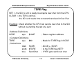
SCCR2 Register
B7 B6 B5 B4 B3 B2
$102D
RE - Receive Enable
TE - Transmit Enable
ILIE - Idle Line Interrupt Enable
RIE - Receive Interrupt Enable
TCIE - Transmit Complete Interrupt Enable
TIE - Transmit Interrupt Enable
Example:
A) Enable the SCI unit for reception only (i.e., need to set the RE bit)
; Address
SCCR2
equ $102D
;Constant
RE
equ
$04
;Instructions
ldaa
staa
#RE
; Load ACCA with control byte
SCCR2 ; Enables SCI for reception
Dalhousie University
136
Jose A. Gonzalez-Cueto
ECED 3204. Microprocessors
Asynchronous Serial Comm
SCI Transmitter Block Diagram
Dalhousie University
137
Jose A. Gonzalez-Cueto
ECED 3204. Microprocessors
Asynchronous Serial Comm
SCI Receiver Block Diagram
Dalhousie University
138
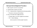
Jose A. Gonzalez-Cueto
ECED 3204. Microprocessors
Asynchronous Serial Comm
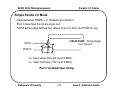
SCSR Register
B7 B6 B5 B4 B3 B2 B1
$102E
0
FE - Framing Error Flag
NF - Noise Error Flag
OR - Over-Run Error Flag
IDLE - Idle Line Detect Flag
RDRF - Receive Data Register Full Flag
TC - Transmit Complete Flag
TDRE - Transmit Data Register Empty Flag
Dalhousie University
139
Jose A. Gonzalez-Cueto
ECED 3204. Microprocessors
Asynchronous Serial Comm
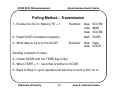
TDRE Flag
SET ⇒ the SCI tx unit is ready to accept a new char from the CPU
CLEAR ⇒ the TDR is still full,
the SCI unit needs time to transmit and avoid Over-Run
Example: Check whether the CPU can send a new char to the SCI
without overwriting the last one sent
; Address Definitions
SCSR
equ
$102E
; Status register address
; Constant Definitions
TDRE
equ
$80
; Mask for TDRE flag in SCSR
; Instructions
ldab
andb
bne
Dalhousie University
SCSR
#TDRE
SendChar
; ACCB ← SCSR
; Is the TDRE flag SET?
; If YES goto send next char
140
Jose A. Gonzalez-Cueto
ECED 3204. Microprocessors
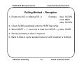
Asynchronous Serial Comm
RDRF Flag
SET ⇒ the SCI rx unit has a new char ready for the CPU to read
CLEAR ⇒ the RDR is empty, no char is available to be read from SCI
Example: Check whether a new char is ready at the SCI for the
CPU to pick up
; Address Definitions
SCSR
equ
$102E
; Status register address
; Constant Definitions
RDRF
equ
$20
; Mask for RDRF flag in SCSR
; Instructions
ldab
andb
bne
SCSR
#RDRF
ReadChar
Dalhousie University
; ACCB ← SCSR
; Is the RDRF flag SET?
; If YES goto read next char
141
Jose A. Gonzalez-Cueto
ECED 3204. Microprocessors
Asynchronous Serial Comm
Polling Method .- Transmission
1.- Enable the SCI tx: Making TE = 1
Example:
2.- Read SCSR (hardware requisite)
3.- Write data to be tx to the SCDR
ldaa SCCR2
oraa #$08
staa SCCR2
ldab SCSR
Example:
ldaa Data
staa SCDR
Sending a stream of chars
4.- Check SCSR until the TDRE flag is Set
5.- When TDRE = ‘1’, next char is written to SCDR
6.- Back to Step 3, cycle repeats until last char is sent to SCI for tx.
Dalhousie University
142
Jose A. Gonzalez-Cueto
ECED 3204. Microprocessors
Asynchronous Serial Comm
Polling Method .- Reception
1.- Enable the SCI rx: Making RE = 1
Example:
ldaa SCCR2
oraa #$04
staa SCCR2
2.- Check SCSR periodically until the RDRF flag is Set
3.- When RDRF = ‘1’, next char is read from SCDR, e.g. ldaa SCDR
4.- Some processing is done if required
5.- Back to Step 2, cycle repeats forever or until reception is finished.
Dalhousie University
143
Jose A. Gonzalez-Cueto
ECED 3204. Microprocessors
Dalhousie University
Asynchronous Serial Comm
144
Jose A. Gonzalez-Cueto
ECED 3204. Microprocessors
Asynchronous Serial Comm
Directing SCI RxD pin PD0 to the
MCU I/O port connector
; Address Definitions
FFLOP
equ
$5000
; Constant Definitions
Byte2Write equ
$00
; Instructions
ldaa #Byte2Write
staa
FFLOP
; A decode address for the FlipFlop
; Bit 0 must be clear, B0 = 0
; ACCA ← 0, clra is an alternative
; Switches PD0 to Target System
Directing SCI RxD pin PD0 to the RS-232 compatible
Host Computer I/O port
; Constant Definitions
Byte2Write equ $0F
; Bit 0 must be set, B0 = 1
; Instructions
ldaa #Byte2Write ; ACCA ← $0F
staa FFLOP
; Switches PD0 to Host Comp I/O port
; to communicate over an RS-232
; protocol (with the PC in our case)
Dalhousie University
145
Jose A. Gonzalez-Cueto
ECED 3204. Microprocessors
Asynchronous Serial Comm
MC6850 (ACIA) Register Selection
Register Select
Input (RS)
R/W
Register
Selected
1
0
Tx Data
Register (TDR)
1
1
Rx Data
Register (RDR)
0
0
Control Register
(CR)
0
1
Status Register
(SR)
Dalhousie University
146
Jose A. Gonzalez-Cueto
ECED 3204. Microprocessors
Asynchronous Serial Comm
Bibliography for Interrupts & the SCI unit
Textbook
- Section 2.1.3
- Section 2.2.2
- Section 2.3.1
- Section 3.9
- Sections 4.2.2, 4.2.3 & 4.3
HC11 Reference Manual (Pink Book)
- Section 5.5 Interrupt Process
- Section 9.5.2 Interrupts & Status Flags (SCI tx)
- Section 9.6.4 Receive Status Flags & Interrupts
Dalhousie University
147
Jose A. Gonzalez-Cueto
ECED 3204. Microprocessors
Asynchronous Serial Comm
Interrupt Acknowledgement Procedure
1. Main program execution is suspended
2. Program state is saved to the stack
3. PC ← Interrupt Vector of highest priority interrupt pending
• Execution continues at this address
4. ISR is concluded with an RTI instruction
• Program state, ie. all CPU registers are restored
• PC ← Return Address,
where execution of main program resumes
Dalhousie University
148
Jose A. Gonzalez-Cueto
ECED 3204. Microprocessors
Asynchronous Serial Comm
Example of SCI Interrupt Service Routine (ISR)
; Address Definitions
SCSR
equ
$102E
SCDR
equ
$102F
; Status register address
; Data register address
; Constant Definitions
RDRF
equ
$20
; Mask for RDRF flag in SCSR
; Instructions
SCI_isr
ldaa
bita
bne
; ACCA ← SCSR (SCI status)
; Is there a new available char?
; If YES goto service rx
SCSR
#RDRF
SCI_rx_isr
Check / service causes other than
RDRF, or just branch to rti at the end
SCI_rx_isr
ldaa
SCDR
; Read available char from SCI
Service reception
rti
Dalhousie University
; Return from ISR
149
Jose A. Gonzalez-Cueto
ECED 3204. Microprocessors
Asynchronous Serial Comm
Interrupt Vector Jump Table
Dalhousie University
150
Jose A. Gonzalez-Cueto
ECED 3204. Microprocessors
Asynchronous Serial Comm
Example of EVB Jump Table Update for SCI
; Address Definitions
SCI_JMPTBL1 equ $00C4
SCI_JMPTBL2 equ $00C5
; JMP OpCode Address in Table for SCI
; Start of Jump Address in Table for SCI
; Constant Definitions
JMPOpCode
equ $7E
; OpCode for JMP instruction
; Instructions
ldaa
staa
ldx
stx
#JMPOpCode
SCI_JMPTBL1
#$C400
SCI_JMPTBL2
; ACCA ← JMP OpCode
; Storing OpCode to table
; IX ← SCI ISR address
; Storing Jump Address to table
Other initialization instructions
SCI_isr
aorg $C400 ; Code to follow loaded at $C400
<1st Instruction of SCI ISR>
Dalhousie University
151
Jose A. Gonzalez-Cueto
ECED 3204. Microprocessors
M68HC11 Timer System
Timer System Functions & Port A Pins
PA7
PA6
PA5
PA4
PA3
PA2
PA1
PA0
Dalhousie University
OC1
OC2
OC3
OC4
P
O
R
T
HC11
TIMER
OC5
IC1 SYSTEM
IC2
IC3
A
152
Jose A. Gonzalez-Cueto
ECED 3204. Microprocessors
M68HC11 Timer System
Main Timer System Block Diagram
Dalhousie University
153
Jose A. Gonzalez-Cueto
ECED 3204. Microprocessors
M68HC11 Timer System
Selecting the Free-running Counter Frequency
(for an E-clock freq = 2 MHz)
Prescale
Counter
Counter
Updates Every Clock Freq
Factor
PR1
PR0
0
0
1
500 ns
2 MHz
0
1
4
2 µs
0.5 MHz
1
0
8
4 µs
250 KHz
1
1
16
8 µs
125 KHz
Dalhousie University
154
Jose A. Gonzalez-Cueto
ECED 3204. Microprocessors
M68HC11 Timer System
Flag Register TFLG1
B7 B6 B5 B4 B3 B2 B1 B0
$1023
IC3F
IC2F
IC1F
OC5F
OC4F
OC3F
Example:
Clearing OC3F
OC3F equ
TFLG1 equ
ldaa
staa
%00100000
$1023
#OC3F
TFLG1
OC2F
OC1F
Dalhousie University
155
Jose A. Gonzalez-Cueto
ECED 3204. Microprocessors
M68HC11 Timer System
Example .- Updating TOC2 for a 1.5ms interval
(Counter clock = 2MHz)
TCNT
TOC2
Increment
equ
equ
equ
$100E
$1018
!3000
; Address of TCNT register
; Address of TOC2 register
; Increment in decimal
Initialization
(1st time)
ldd
TCNT
addd #Increment
std
TOC2
Part of ISR
or
Successful
Polling
ldd
TOC2
addd #Increment
std
TOC2
Dalhousie University
156
; Hardware detail:
; When TOC2HI is written
; compares are suspended
; for 1 E-clock cycle
Jose A. Gonzalez-Cueto
ECED 3204. Microprocessors
M68HC11 Timer System
Controlling Port A Pin State
Timer Control Register 1 (TCTL1)
B7
B6
B5
B4
B3
B2
B1
B0
$1020 OM2 OL2 OM3 OL3 OM4 OL4 OM5 OL5
RESET = 0
OMX OLX
0
0
Action Taken
0
0
None
(Disconnected)
0
1
Toggle OCX line
1
0
Clear OCX line
(logic ‘0’)
1
Set OCX line
(logic ‘1’)
1
Dalhousie University
0
0
0
0
0
Example:
Setting PA5 to toggle on each
successful compare with TOC3
CTLBYTE equ %00010000
TCTL1
equ $1020
ldaa #CTLBYTE
staa TCTL1
157
Jose A. Gonzalez-Cueto
ECED 3204. Microprocessors
M68HC11 Timer System
Local IC/OC Timer Interrupt Masks
Interrupt Enable Register 1 (TMSK1)
B7
B6
B5
B4
B3
B2
B1
B0
$1022 OC1I OC2I OC3I OC4I OC5I IC1I IC2I IC3I
RESET = 0
0
0
When ‘0’ = Interrupt Inhibited
‘1’ = Interrupt Enabled
0
0
0
0
0
Example:
Enabling Interrupts from TOC4
OC4I
TMSK1
equ %00010000
equ $1022
ldaa TMSK1
oraa #OC4I
staa TMSK1
Dalhousie University
158
Jose A. Gonzalez-Cueto
ECED 3204. Microprocessors
M68HC11 Timer System
Selecting Port A Triggering Event
Timer Control Register 2 (TCTL2)
$1021
EDGXB
EDGXA
B7
B6
0
0
Configuration
0
0
Capture Disabled
0
1
Capture on Rising
Edges Only
1
0
Capture on Falling
Edges Only
1
Capture on Any
Edge (Rising or
Falling)
1
Dalhousie University
159
B5
B4
B3
B2
B1
B0
EDG3A
EDG3B
EDG2A
EDG2B
EDG1A
EDG1B
Jose A. Gonzalez-Cueto
ECED 3204. Microprocessors
M68HC11 Timer System
Example .- Period Measurement using TIC3 (PA0)
TIC3
TCTL2
CTLBYTE
equ
equ
equ
$1014
$1021
%00000001
Initialization
ldaa
staa
# CTLBYTE
TCTL2
Part of ISR
or
Successful
Polling
ldd TIC3
subd PreviousReading
std Period
ldd TIC3
std PreviousReading
<clear IC3F>
PreviousReading
Period
Dalhousie University
ds
ds
; Rising edge
; Period = TICnew - TICold
; Update TICold
; TICold
; Current period
2
2
160
Jose A. Gonzalez-Cueto
ECED 3204. Microprocessors
M68HC11 Timer System
Example .- Pulse Width Measurement using TIC3 (PA0)
CTLBYTE1
CTLBYTE2
Initialization
equ %00000001;
equ %00000010;
Rising edge
Falling edge
ldaa # CTLBYTE1
staa TCTL2
< EdgeFlag ← Rising >
Part of ISR
or
Successful
Polling
- If EdgeFlag == Rising ?
ldd TIC3
std FirstEdge
< EdgeFlag ← Falling >
ldaa #CTLBYTE2
; Enable falling
staa TCTL2
; edge detection
Dalhousie University
161
Jose A. Gonzalez-Cueto
ECED 3204. Microprocessors
M68HC11 Timer System
Example .- Pulse Width Measurement (cont’d)
- If EdgeFlag == Falling ?
ldd TIC3
Part of ISR
or
Successful
Polling
FirstEdge
PWidth
EdgeFlag
subd FirstEdge
std PWidth
< EdgeFlag ← Rising >
ldaa #CTLBYTE1
; Enable rising
staa TCTL2
; edge detection
ds
ds
ds
Dalhousie University
2
2
1
162
Jose A. Gonzalez-Cueto
ECED 3204. Microprocessors
M68HC11 Timer System
Using IC Timer Interrupts:
1) Set the EVB jump vector for the corresponding IC function
2) Enable TIC Function in TCTL2
3) Enable local interrupt mask ICxI
4) Enable global interrupt mask (I-flag in CCR)
Example:
Enabling interrupts from TIC3 (Step 3 above)
TMSK1
IC3I
equ
equ
$1022
; Address of TMSK1 register
%00000001 ; IC3I Mask
Part of
Initialization
ldaa
oraa
staa
TMSK1
#IC3I
TMSK1
Dalhousie University
163
Jose A. Gonzalez-Cueto
ECED 3204. Microprocessors
M68HC11 Timer System
Example .- Generating a 1 sec Delay with TOCx
1. Delay interval is triggered (1st time):
ldaa
staa
ldd
addd
std
bra
#!30
Counter
TOCx
#!33920
TOCx
Return
Counter
Initialization
OCx successful compare
TOCx
Initialization is triggering the interval
2. With every SUCCESSFUL COMPARE (after 1st time above):
dec
Counter
; Decrement Counter
bmi
ExecTask
; Check if Counter < 0
bra
Return
; If NOT keep decrementing it
ExecTask jsr
ProcessX
; If YES take action
<Deactivate TOCx interrupt> ; for a One-time Task
Return
<clear OCxF>
rti
Dalhousie University
164
Jose A. Gonzalez-Cueto
ECED 3204. Microprocessors
M68HC11 Timer System
Example .- Generating a 2 sec Square Wave in PA6 (TOC2)
TOC2_isr ldaa Counter
bne
CountDown
ldaa #!30
Counter
staa Counter
Initialization
ldd
TOC2
If Counter is 0,
Update
addd #!33920
Initialize TOC2
TOC2
std
TOC2
& Counter
ldaa TCTL1
Disconnect TOC2
anda #%00111111
from output pin
staa TCTL1
logic (PA6 )
bra
Return
CountDown dec
Counter
bne
Return
When Counter reaches 0,
ldaa TCTL1
oraa %01000000 set PA6 line to toggle its
value with next TOC2
staa TCTL1
successful compare
Return
< clear OC2F >
rti
Dalhousie University
165
Jose A. Gonzalez-Cueto
ECED 3204. Microprocessors
M68HC11 Timer System
Example .- Generating a 2 sec Square Wave (cont’d)
TOC2_init
(1) < Counter ← 0 >
(2) Set PA6 logic to toggle its value with the next
TOC2 successful compare
(3) Set up TOC2 interrupt vector (e.g. EVB jump
table)
(4) Clear OC2F
(5) Enable TOC2 interrupts
i.e. OC2I ← 1
Dalhousie University
166
Jose A. Gonzalez-Cueto
ECED 3204. Microprocessors
M68HC11 Timer System
Measuring Long Periods
TIC_isr
« Find & Save: TIC∆ = TICnew − TICold »
« If TIC∆ < 0, Counter ← Counter − 1 »
- Assuming 5000 E-clk cycles
« If TICnew < 5000d
(PR0 = PR1 = 0) are sufficient
« read TOF »
Detecting & Solving
to have OF serviced before IC.
« If TOF is SET, - Avoids wrong correction when
a Missed Overflow
inc Counter TICnew < $FFFF but close to it.
IncFlag ← 0 » »
« Save Counter » ; Preparing for measuring
clr Counter
; next period
« clear ICxF flag » ; Acknowledge interrupt service
rti
OF_isr
« If IncFlag is SET,
inc Counter »
« IncFlag ← 1 »
« clear TOF flag » ; Acknowledge interrupt service
rti
Dalhousie University
167
Jose A. Gonzalez-Cueto
ECED 3204. Microprocessors
M68HC11 Timer System
Solving a Missed Overflow (Alternative − No IncFlag)
TIC_isr
« Find & Save: TIC∆ = TICnew − TICold »
« If TIC∆ < 0, Counter ← Counter − 1 »
« If TICnew < 5000d
Detecting & Solving
« read TOF »
a Missed Overflow
« If TOF is SET,
inc Counter
Save Counter
; Preparing for measuring
Counter ← $FF ; next period if OF missed
else
Save Counter
; Preparing for measuring
Counter ← $00 » ; next period if OF serviced
else Save Counter, Counter ← $00 »
« clear ICxF flag »
; Acknowledge interrupt service
rti
OF_isr
incCounter
« clear TOF flag »
rti
Dalhousie University
; Acknowledge interrupt service
168
Jose A. Gonzalez-Cueto
ECED 3204. Microprocessors
M68HC11 Timer System
Hex to ACD (ASCII-coded
(ASCII
decimal)
• HtoD Subroutine - Example
Dalhousie University
169
Jose A. Gonzalez-Cueto
ECED 3204. Microprocessors
Parallel I/O Comm
Parallel PORTB Control of a
Two Digit Common-Anode 7-Segment LED Display
Dalhousie University
170
Jose A. Gonzalez-Cueto
ECED 3204. Microprocessors
Parallel I/O Comm
MC68HC11 Block Diagram
Dalhousie University
171
Jose A. Gonzalez-Cueto
ECED 3204. Microprocessors
Parallel I/O Comm
I/O Transfer Synchronization
The role of an I/O interface unit
1. Synchronizing data transfer between CPU and I/O interface unit.
2. Synchronizing data transfer between I/O interface and I/O device.
Data Bus
Microprocessor
CPU
Control
signals
(R/W or
interrupt)
I/O
Interface
Handshake
or Strobe
Signals
I/O device
Data Bus
Dalhousie University
172
Jose A. Gonzalez-Cueto
ECED 3204. Microprocessors
Parallel I/O Comm
Synchronizing the Microprocessor CPU and the I/O Interface Unit
The polling method
1. for input -- the CPU checks a status bit of the interface unit to find out if the
interface unit has received new data from the input device.
2. for output -- the CPU checks a status bit of the interface unit to find out if it
can send new data to the interface unit.
The interrupt-driven method
1. for input -- the interface unit interrupts the CPU whenever it has received
new data from the input device.
2. for output -- the interface unit interrupts the CPU whenever it can accept
new data from the CPU.
Dalhousie University
173
Jose A. Gonzalez-Cueto
ECED 3204. Microprocessors
Parallel I/O Comm
Synchronizing the I/O Interface Unit and I/O Devices
Brute-force method -- useful when the data timing is unimportant
1. for input -- nothing special is done. The CPU reads the interface unit and the
interface unit returns the voltage levels on the input port pins to the CPU.
2. for output -- nothing special is done. The interface unit places the data that it
received from the CPU directly on the output port pins.
The strobe method -- a strobe signal is used to indicate that data are stable on
I/O port pins
1. for input -- the interface unit latches the data into its data register using the
strobe signal.
2. for output -- a) the interface unit places the data received from the CPU on
the output port pins and asserts the strobe signal.
b) the output device latches the data using this strobe signal.
Dalhousie University
174
Jose A. Gonzalez-Cueto
ECED 3204. Microprocessors
Parallel I/O Comm
Synchronizing the Interface Unit and I/O Devices (cont’d)
The handshake method -- used when timing is crucial
• For input and output,
- Two handshake signals are used to synchronize the data transfer:
1. One signal, call it H1, is asserted by the interface unit.
2. The other signal, call it H2, is asserted by the I/O device.
• Two handshake modes are available -- pulse mode and interlocked mode.
Dalhousie University
175
Jose A. Gonzalez-Cueto
ECED 3204. Microprocessors
Parallel I/O Comm
Input Handshake Protocol
Step 1. The interface unit asserts (or pulses) H1 to indicate its intention to input data.
Step 2. The input device puts data on the data port pins and also asserts (or pulses) the
handshake signal H2.
Step 3. The interface unit latches the data and de-asserts H1.
After some delay, the input device also de-asserts H2.
H1
Data
Valid Data
H2
(a) Interlocked
H1
Data
Valid Data
H2
(b) Pulse mode
Dalhousie University
176
Jose A. Gonzalez-Cueto
ECED 3204. Microprocessors
Parallel I/O Comm
Output Handshake Protocol
Step 1. The interface unit places data on the port pins and asserts (or pulses) H1 to
indicate that it has valid data to be output.
Step 2. The output device latches the data and asserts (or pulses) H2 to acknowledge
the receipt of data.
Step 3. The interface unit de-asserts H1 following the assertion of H2. The output device
then de-asserts H2.
H1
Data
H2
Valid Data
(a) Interlocked
H1
Data
H2
Dalhousie University
Valid Data
(b) Pulse Mode
177
Jose A. Gonzalez-Cueto
ECED 3204. Microprocessors
Parallel I/O Comm
Parallel I/O Control Register (PIOC)
- All strobed mode I/O and handshake I/O are controlled by this register
7
6
5
4
3
STAF STAI CWOM HNDS OIN
Upon RESET
0
0
0
0
0
2
1
0
PLS
EGA
INVB
U
1
1
$1002
STAF: Strobe A flag
This bit is set when a selected edge occurs on the STRA signal.
STAI: Strobe A interrupt enable
When STAF = STAI = ‘1’, an interrupt is requested to the CPU.
CWOM: Port C wired-or mode
.
0: All port C outputs are normal CMOS outputs.
1: All port C outputs act as open-drain outputs.
HNDS: Handshake/simple strobe mode select
0: simple strobe mode
1: handshake mode
OIN: Output/input handshake
0: input handshake
1: output handshake
PLS: Pulse/interlocked handshake operation
0: interlocked handshake selected
1: pulse handshake selected
INVB: Invert STRB
0: STRB active low
1: STRB active high
EGA: Active edge for STRA
0: falling edge
1: rising edge
Dalhousie University
178
Jose A. Gonzalez-Cueto
ECED 3204. Microprocessors
Parallel I/O Comm
Simple Strobe I/O Mode
- Selected when HNDS = ‘0’ (default upon RESET)
- Port C becomes the strobe input port.
- STRA active edge latches the values of port C pins into PORTCL reg.
STRA
tIS
(VALID DATA - Rising Edge)
from Device
tIH
PORTC
t IS: input setup time (60 ns at 2 MHz)
t IH : input hold time (100 ns at 2 MHz)
Port C strobed input timing
Dalhousie University
179
Jose A. Gonzalez-Cueto
ECED 3204. Microprocessors
Parallel I/O Comm
Simple Strobe Mode - Input (Port C)
- Bit 1 of the PIOC register (EGA) selects the active edge of the STRA pin.
- Reading PORTC register returns the current values on Port C pins.
- Reading PORTCL register returns Port C values latched with last STRA
active edge.
- When enabled (STAI = ‘1’), the active edge of the STRA signal will request
an interrupt to the CPU.
- The STRA interrupt vector is at $FFF2:FFF3 (same as for IRQ pin).
- STAF clearing sequence:
1. Read PIOC register.
2. Read PORTCL register.
Dalhousie University
180
Jose A. Gonzalez-Cueto
ECED 3204. Microprocessors
Parallel I/O Comm
Simple Strobe Mode - Output (Port B)
The strobe signal STRB is pulsed for two E clock cycles each time there is a
write to port B.
CPU write
to PORT B
E
t PWD
new port data
Port B previous port data
tDEB
STRB
tPWD : peripheral data write delay time
tDEB : E fall to STRB valid delay time
(VALID DATA)
for 2 E cycles
from
HC11
port
(Active High)
Port B strobed output timing
Dalhousie University
181
Jose A. Gonzalez-Cueto
ECED 3204. Microprocessors
Parallel I/O Comm
Port C Interlocked Input Handshake Protocol
Read
PORTCL
E
STRB
(ACK* - Active High)
from HC11 Port to Device
"READY"
STRA
"READY"
(VALID DATA - Rising Edge)
from Device to HC11 Port
PORTC
* ACK - Acknowledge line / signal
Dalhousie University
182
Jose A. Gonzalez-Cueto
ECED 3204. Microprocessors
Parallel I/O Comm
Port C Input Handshake Protocol
- STRA is a valid data latch command asserted by the input device (active
edge is rising in previous figure).
- STRB is an acknowledge/ready output driven by the 68HC11 (active high in
figure).
- When ready for accepting new data, the HC11 asserts (or pulses) STRB pin.
- The input device places data on port C pins and asserts the STRA signal.
1) The active edge of STRA latches data into the PORTCL register,
2) Sets the STAF flag in PIOC register, and
3) De-asserts the STRB signal.
• The de-assertion of STRB inhibits the external device from strobing new
data into port C.
• New data can be applied on port C pins once the CPU reads PORTCL.
- STAF clearing sequence:
1. Read PIOC register.
2. Read PORTCL register.
Dalhousie University
183
Jose A. Gonzalez-Cueto
ECED 3204. Microprocessors
Parallel I/O Comm
Port C Interlocked Output Handshake Protocol
WRITE
PORTCL
E
tPWD
PORT C previous data
new port data
tDEB
tDEB
STRB
(VALID DATA - Active High)
from HC11 Port to Device
DATA READY
tAES
STRA
(ACK - Active High)
from Device to HC11 Port
t PWD : Peripheral data write delay time, 150 ns max (at 2 MHz)
t DEB : E fall to STRB delay, 225 ns (at 2 MHz)
t AES : STRA asserted to E fall setup time, 0 ns (at 2 MHz)
Dalhousie University
184
Jose A. Gonzalez-Cueto
ECED 3204. Microprocessors
Parallel I/O Comm
Port C Output Handshake Protocol
- STRA is an acknowledge input (driven by the external device)
- STRB is a valid data or data ready output (driven by the 68HC11)
- In the figure, STRA activates with rising edge and STRB is active high.
Protocol sequence:
(a) The 68HC11 writes data into PORTCL and then asserts STRB to indicate
that there are valid data on port C pins.
(b) The external device then asserts STRA to acknowledge the receipt of
data which will then cause STRB to be de-asserted and the STAF flag to be
set.
(c) After the de-assertion of STRB, STRA is also de-asserted.
- STAF clearing sequence:
1. Read PIOC register.
2. Write PORTCL register.
Dalhousie University
185
Jose A. Gonzalez-Cueto
ECED 3204. Microprocessors
Parallel I/O Comm
Code Example using Simple Strobe I/O
; Addresses
PIOC
PORTB
PORTCL
equ
equ
equ
$1002 ; Address for the Parallel I/O Control register
$1004 ; Address for Port B data register
$1005 ; Address for Port C Latched data register
; Constants
BITMASK
equ
$80
; Program Code
org
$C000
loop
ldaa
bita
beq
ldab
stab
bra
#BITMASK
PIOC
loop
PORTCL
PORTB
loop
; Bit mask for STAF flag in PIOC register
; To be loaded at $C000
; ACCA ← STAF bit mask
; Is STAF Set?
; If NOT loop back & wait until it is
; If YES, ACCB ← data latched in PORTCL
; Sending latched value just read to Port B
; Branch back and keep polling STAF for
; next valid input data in Port C.
end
Dalhousie University
186
Jose A. Gonzalez-Cueto
ECED 3204. Microprocessors
Parallel I/O Comm
External Parallel Port Example
Dalhousie University
187
Jose A. Gonzalez-Cueto
ECED 3204. Microprocessors
Parallel I/O Comm
Code for Servicing the External Input Port
PSTATUS
PDATA
BUF_START
BUF_END
POLL
equ
equ
equ
equ
$8000
$8001
$D000
$D0FF
; Port Status Address
; Port Data Address
; Start of Buffer
; Last element in Buffer
org
$C000
; Start of code
ldaa
ldx
ldaa
anda
beq
ldaa
staa
inx
cpx
bls
swi
PDATA
; Dummy read to clear port status
#BUF_START ; Initialize IX pointer
PSTATUS
; Get current status
#%01000000 ; Check B6 by masking other bits
POLL
; If status is still zero keep polling
PDATA
; If NOT, get data from port
0,X
; Store it in Buffer using IX pointer
; Update Buffer pointer
#BUF_END ; Check if Buffer end has been reached
POLL
; If NOT, go back wait for new data from port
; If YES, exit to BUFFALO
end
Dalhousie University
188
Jose A. Gonzalez-Cueto
ECED 3204. Microprocessors
Parallel I/O Comm
Alternative to define Buffer space
org
BUF_START ds
BUF_END
ds
$D000 ; Start of Buffer
!255
1
; One element less than total space
; Last element (to allow labeling it)
Alternative check for program end
DONE
staa
cpx
beq
inx
bra
swi
0,X
#BUF_END
DONE
POLL
Dalhousie University
; Store it in Buffer using IX pointer
; Check if last element written
; If YES, finish program
; If NOT, update Buffer pointer &
; Go back wait for new data from port
; Exit to BUFFALO
189
Jose A. Gonzalez-Cueto