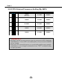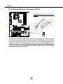
1
R
T h e
S o u l
O f
SL-75DRV2
C o m p u t e r
T e c h n o l o g y
USER MANUAL v1.0
NOTICE
Product Model
Manual Revision
Release Date
: SL-75DRV2
: V1.0
: September 2001
T
his Users Guide & Technical Reference is to help system
manufacturers and end-users set up and install the mainboard.
Every effort has been made to ensure that the information in this
manual is accurate. Soltek Computer Inc. is not responsible for printing or
clerical errors. Information in this document is subject to change
without notice and does not represent a commitment on the part of
Soltek Computer Inc.
No part of this manual may be reproduced, transmitted, translated
into any language in any form or by any means, electronic or
mechanical, including photocopying and recording, for any purpose
without the express written permission of Soltek Computer Inc.
Companies and products mentioned in this manual are for identification
purpose only. Product names appearing in this manual may or may
not be registered trademarks or copyrights of their respective
companies.
Soltek Computer Inc. provides this manual “As is “ without warranty
of any kind, either express or implied, including but not limited to the
implied warranties or conditions of merchantability or fitness for a
particular purpose. In no event shall Soltek Computer Inc. be liable
for any loss or profits, loss of business, loss of use or data, interruption of
business, or for indirect, special, incidental, or consequential damages of
any kind, even if Soltek Computer Inc. has been advised of the possibility
of such damages arising from any defect or error in this manual or product.
Copyright © 2001 Soltek Computer Inc. All Rights Reserved.
• AMD Athlon ThunderbirdTM, and DuronTM processors are trademarks of AMD Corporation.
• VIA, KT-266A, VT8366A and VT8233 are trademarks of VIA Corporation.
• Norton AntiVirus, Norton Ghost are trademarks of Symantec Corporation.
SOLTEK AROUND THE WORLD
SOLTEK COMPUTER INC.
Address
Telephone
Fax
E-mail
Web site
: 7F, No. 306-3, Ta-Tung Rd, Sec.1, Hsi-Chih, TaipeiHsien, Taiwan, R.O.C.
: 886-2-2642-9060
: 886-2-2642-9065
: [email protected]
: http://www.soltek.com.tw
SOUL TECHNOLOGY EUROPE B.V.
Address
Telephone
Fax
E-mail
Web site
: Hongkongstraat 55, 3047 BP Rotterdam. The Netherlands
: 31-10-2457492
: 31-10-2457493
: [email protected]
: http://www.soultech-europe.com
75DRV2/
CONTENT
CHAPTER 1 INTRODUCTION ............................................... 8
1-1 MAINBOARD SPECIFICATION ................................................. 9
1-1.1 PROCESSOR ................................................................................... 9
1-1.2 CHIPSET ........................................................................................... 9
1-1.3 AWARD BIOS V6.0 SUPPORTING ................................................... 9
1-1.4 SOUND CONTROLLER .................................................................... 9
1-1.5 POWER MANAGEMENT .................................................................. 9
1-1.6 FULL FEATURED ACCELERATED GRAPHICS PORTS (AGP)
CONTROLLER ................................................................................ 10
1-1.7 MULTI-I/O FUNCTION .................................................................... 10
1-1.8 EXPANSION SLOTS ....................................................................... 10
1-1.9 ADVANCED HIGH PERFORMANCE SDR/DDR DRAM ................. 10
CONTROLLER ................................................................................ 10
1-1.10 FORM FACTOR ............................................................................ 11
1-1.11 HARDWARE MONITOR ................................................................ 11
1-2 MAINBOARD LAYOUT ............................................................ 12
1-3 CHIPSET DIAGRAM ................................................................ 13
CHAPTER 2 HARDWARE SETUP ....................................... 15
2-1 CPU INSTALLATION ............................................................... 16
2-2 MEMORY INSTALLATION ....................................................... 17
2-3 ACCELERATED GRAPHICS PORT(AGP) PRO INSTALLATION ... 19
2-4 HDD/FDD INSTALLATION ....................................................... 20
2-5 SWITCH SETTING FOR CPU FREQUENCY AND VOLTAGE 22
2-5.1 Information On AMD Socket 462 Processor (Model 4, 5 Products) ... 22
2-5.2 Information On AMD Socket 462 Processor (Model 6, 7 Products) ... 23
4
Content
2-5.3 Frequency Ratio Select (By SW1 DIP1-DIP5) ................................ 24
2-5.4 Processor Core Voltage Select (By SW2 DIP1-DIP6) ..................... 25
2-5.5 CPU External Frequency Setting (By SW3) .................................... 26
2-6 JUMPER SETTING FOR DEVICES ON BOARD .................... 27
2-6.1 JP1/JP2 Memory Module Voltage Select ........................................ 27
2-6.2 JP17 Power Lost Resume ............................................................... 28
2-6.3 JP18/19 AGP Voltage Select ........................................................... 28
2-6.4 JBAT1 For Clear CMOS Data ......................................................... 29
2-7 CONNECTORS CONFIGURATIONS ...................................... 30
2-7.1 On Board FAN Connector (FAN1, FAN2, FAN3, FAN4) .................. 30
2-7.2 WOL1 Wake On LAN ...................................................................... 31
2-7.3 CD-ROM Audio Connector (JCD_IN1) ............................................ 31
2-7.4 Thermal Sensor Connector (RT2) ................................................... 32
2-7.5 Complex Header CON1 .................................................................. 33
2-7.6 ATX Power Supply Connector ......................................................... 34
2-7.7 Chassis Panel Connector ............................................................... 35
2-7.8 Smart Card Reader Connector (SCR1) .......................................... 36
2-7.9 Communication And Networking Riser Slot (CNR) ......................... 37
2-7.10 USB Header (USB2/USB3 Header) .............................................. 38
2-7.11 PS/2 Mouse And PS/2 Keyboard .................................................. 38
CHAPTER 3 SOFTWARE SETUP ....................................... 40
3-1 OPEN UP THE SUPORT CD AND CHOOSE DRIVERS AND
UTILITIES ................................................................................ 41
3-2 PROCEED TO VIA 4-IN-1 DRIVERS INSTALLATION ............ 42
3-3 PROCEED TO AC’97 AUDIO DRIVER INSTALLATION .......... 44
3-4 PROCEED TO HARDWARE MONITOR INSTALLATION ....... 45
5
75DRV2/
CHAPTER 4 BIOS SETUP ................................................... 48
4-1 WHAT IS BIOS SETUP ............................................................ 49
4-2 HOW TO RUN BIOS SETUP ................................................... 49
4-3 WHAT IS CMOS ...................................................................... 49
4-4 WHAT IS POST ....................................................................... 49
4-5 BIOS UPGRADE ..................................................................... 49
4-5.1 BEFORE UPGRADING BIOS ......................................................... 50
4-5.2 UPGRADE PROCESS .................................................................... 50
4-6 BIOS SETUP --- CMOS SETUP UTILITY ................................ 54
4-6.1 CMOS SETUP UTILITY .................................................................. 54
4-6.2 STANDARD CMOS SETUP ............................................................ 55
4-6.3 ADVANCED BIOS FEATURES ....................................................... 58
4-6.4 ADVANCED CHIPSET FEATURES ................................................ 62
4-6.5 INTEGRATED PERIPHERALS ....................................................... 67
4-6.6 POWER MANAGEMENT SETUP ................................................... 73
4-6.7 PNP / PCI CONFIGURATION ......................................................... 79
4-6.8 SMARTDOC ANTI-BURN SHIELD ................................................. 82
4-6.9 FREQUENCY/VOLTAGE CONTROL .............................................. 84
4-6.10 LOAD OPTIMIZED DEFAULTS ..................................................... 87
4-6.11 SET SUPERVISOR / USER PASSWORD .................................... 87
4-6.12 SAVE & EXIT SETUP .................................................................... 88
4-6.13 EXIT WITHOUT SAVING .............................................................. 88
APPENDICES ......................................................................... 90
APPENDIX-1 IDENTIFY BIOS VERSION & BIOS PART NUMBER ... 91
APPENDIX-2 IDENTIFYING MAINBOARD MODEL NUMBER .... 92
APPENDIX-3 TECHNICAL TERMS ............................................... 93
6
Content
ITEM LIST CHECKUP
Mainboard
====
Support CD
====
User’s Manual
====
Bundled Bonus Pack CD
====
Bundled Bonus Pack Manual
====
Temperature Sensor Cable
====
ATA66/100 IDE Cable
====
RS232 Cable
FDD Cable
7
75DRV2
CHAPTER
1
INTRODUCTION
• This chapter briefly introduces the characteristics of the mainboards. It includes
the information regarding the chipset, CPU types, built-in functions and layout.
Users will have more ideas about mainboards after reading this chapter.
This chapter contains the following topics :
1-1 MAINBOARD SPECIFICATION
1-2 MAINBOARD LAYOUT
1-3 CHIPSET DIAGRAM
8
Chapter 1 Introduction
1-1 MAINBOARD SPECIFICATION
1-1.1 PROCESSOR
• Supporting Socket A-based AMD Athlon™/Duron™/Athlon 4™ processors.
• Supporting 200MHz & 266MHz FSB bus.
• Supporting Processor VID(voltage ID) and FID(Frequency ID) auto
detection.
1-1.2 CHIPSET
• North Bridge: VIA VT8366A KT-266A.
• South Bridge: VIA VT8233.
• LPC I/O ITE 8705.
1-1.3 AWARD BIOS V6.0 SUPPORTING
• Plug & Play V1.0.
• Flash Memory for easy upgrade.
• Year 2000 compliant.
• BIOS writing protection.
• SmartDOC Anti-Burn shield.
1-1.4 SOUND CONTROLLER
• SoundBlaster Pro Hardware and Direct Sound Ready AC97 Digital Audio
Controller with Codec onboard.
1-1.5 POWER MANAGEMENT
• ACPI 1.0 compliant (Advanced Configuration and Power Interface).
• APM V1.2 compliant (legacy power management).
• Supporting ACPI suspend STR mode (Suspend To DRAM) and POS mode
(Power On Suspend).
• System event monitoring with two event classes.
• Supporting PS/2 Keyboard & Mouse power on.
• Supporting Wake On LAN (WOL) & Wake On Modem.
• Supporting real time clock (RTC) with date alarm, month alarm, and century
field.
• USB boot-up Function.
9
75DRV2
1-1.6 FULL FEATURED ACCELERATED GRAPHICS PORTS
(AGP) CONTROLLER
• AGP v2.0 compliant.
• Supports Side Band Addressing(SBA) mode (non-multiplexed address /
data).
• Supporting 66MHz 1x, 2x, and 4x modes for AD and SBA signaling.
1-1.7 MULTI-I/O FUNCTION
• Two UltraDMA-33/66/100 Master Mode PCI EIDE ports.
• Two UARTs for complete Serial Ports.
• One dedicated IR connector:
-- At third serial port dedicated to IR function either through the two complete serial
ports or the third dedicated port Infrared-IrDA (HPSIR) and ASK( Amplitude Shift
Keyed) IR.
• Multi-mode parallel connector supporting:
-- Standard mode, ECP and EPP.
• Floppy Disk connector supporting:
-- One FDDs with drive swap function.
• Universal Serial Bus connector supporting:
-- USB v1.1 and Intel Universal HCI v1.1 compatible.
-- 2 built-in USB connectors, in addition to one internal USB header which requires
a USB cable to support 2 more optional USB ports.
• PS/2 keyboard connector.
• PS/2 Mouse connector.
1-1.8 EXPANSION SLOTS
• Five PCI bus Master slots.
• One CNR slot.
• One AGP PRO 4x mode slot.
• Three 184-pin DIMM slots.
• One SCR (Smart Card Reader) slot.
1-1.9 ADVANCED HIGH PERFORMANCE SDR/DDR DRAM
CONTROLLER
• Supporting memory size up to 3GB.
• Supporting 184-pin DDR SDRAM type only.
• Supporting PC1600 and PC2100 DDR SDRAM.
10
Chapter 1 Introduction
1-1.10 FORM FACTOR
• ATX form factor, 4- layer PCB.
• Mainboard size 22.0cm x 30.5cm.
1-1.11 HARDWARE MONITOR
• Programmable control, status to provide, monitoring and alarm for flexible
desktop management (software include).
• 5 positive voltage statuses monitoring.
• 2 temperatures statuses monitoring.
• 2 Fan-speeds statuses monitoring.
11
75DRV2
5
3
PS/2
K/B
4
3
2
1
6
ON
DIP
5
4
3
2
1
1
3
FAN2
FAN1
DIP
SW1
ON
DDR 266
1
CN1
SW2
SOCKET A
USB0
USB1
PS/2
MOUSE
1-2 MAINBOARD LAYOUT
RT1
VIA
VT8366A
GAME/MIDI PORT
ZD1
FAN4
3
3
1
Clock
Generator
AGP PRO 4X
1
1
JP1
JP2
5
SW3
1
ON
2
3
4
DIP
3
MIC
LINE
IN
LINE
OUT
COM2
COM1
LPT1
SSF1
FDC1
JP18
JP19
1
1
PCI 2
IDE2
PCI 3
RT2
SLED
-
3
+
PLED
JBAT1
PCI 5
RST
1
16
USB3
1
16
1
SCR1
3
FAN3
1
SAPK
JP17
USB2
CNR 1
30
1
15
VIA
VT8233
PCI 4
IR
3
WOL1
CON1
FLASH BIOS
1
Li
Battery
SUSPEND
LPC I/O
Controller
IDE1
PWR
JCD_IN1
HDD/LED
+ - - +
4
1
1
16
PCI 1
3
3
AC'97
Codec
3
Using non-compliant memory with higher bus clock (over clocking) may
severely compromise the integrity of system.
12
Chapter 1 Introduction
1-3 CHIPSET DIAGRAM
• The VT8366A and VT8233 chipset is a high performance, cost-effective
and energy efficient system controller for the implementation of AGP /
PCI / ISA desktop personal computer system based on 64-bit Socket-A
(AMD Athlon) processors.
SYSCLK, SYSCLK#
PROCRDY
CONNECT
CFWDRST
Athlon
Host CPU
3D
Graphics
Controller
Address
Out
INTR, NMI, SM#, STPCLK#,
IGNNE#, FERR#, A20M#,
Data
PWROK, INIT#, RESET#
In
CKE#
SDR/DDR Memory Bus
GCLK
VT8366A
AGP Bus
DDR Vlink
Host North
552 BGA
GCKRUN#
SDR/VCM
& DDR
SDRAM
MCLK
HCLK
Clock
Buffer
PCLK
CPUSTP#
SUSCLK,
PCKRUN#
Clock
Generator
SUSST1#
PCISTP#
PCI Bus
VT8233
PCLK
ATA33/66/100
MII/LAN
6x USB
Vlink
Client South
352 BGA
SMBus
Power Plan & Peripheral Control
GPIO and ACPI Events
LPC
Diagram of Apollo Pro266A System Block Using the VT8233 V-Link
South Bridge
13
75DRV2
MEMO
MEMO
14
Chapter 2 Hardware Setup
CHAPTER
2
HARDWARE SETUP
ATTENTION !!!
1. Please refer to your processor installation or other
documentation attached to your CPU for detailed installing instruction.
2. Installing a heat sink and cooling fan is necessary
for proper heat dissipation from your CPU. Incorrect
installation may result in overheating and damage
of your CPU.
3. Before changing the setting of CPU Vcore from BIOS
program, user SHOULD make sure of correct specification both of CPU CLOCK and RATIO. Incorrect
setting may cause damage to your CPU.
This chapter contains the following topics :
2-1 CPU INSTALLATION
2-2 MEMORY INSTALLATION
2-3 AGP PRO INSTALLATION
2-4 HDD/FDD INSTALLATION
2-5 SWITCH SETTING FOR CPU FREQUENCY AND
VOLTAGE
2-6 JUMPER SETTING FOR DEVICES ON BOARD
2-7 CONNECTORS CONFIGURATION
15
75DRV2
2-1 CPU INSTALLATION
WARNING !!!
• Make sure that +5V DCV and +3.3 DCV capabilities of your power supply
are suitable for the processor.
• Any attempt to operate the AMD Athlon or Duron processor without a
suitable cooling Fan will damage processor and other component.
Pull out the lever from the
socket, and then raise the
lever up to a 90-degree angle.
S
O
C
K
E
T
46
2
1
2
AMD
SO
C
T
KE
462
A
M
D
3
SO
E
CK
T4
62
16
Take notice of the red circles
as shown below. While inserting
the CPU into the socket, you
can find out there is a definite
pin orientation for CPU and
socket.
Make sure that the CPU is
placed into the socket tightly.
Then lower down the level to
complete the CPU installation.
Chapter 2 Hardware Setup
2-2 MEMORY INSTALLATION
WARNING!!!
• Make sure to unplug your power supply before adding or removing memory
modules or other system components. Failure to do so may cause severe
damage to both your mainboard and expansion cards.
• Be careful when inserting or removing DIMM. Forcing a DIMM in or out
of a socket improperly may damage the memory module or the socket.
Some DIMMs which contain EDO or FTP DRAM are incompliant with
the mainboard. The M/B supports 2.5V DDR SDRAM only.
Installing DIMM
• Make sure you have the correct memory module type for your mainboard.
• Insert the module(s) as shown below, DIMMs have 184-pins and one notch
that will be matched by the onboard DIMM socket. Memory modules are
installed by inserting them straight into the slot until they “click” in the right
place. They only fit in one direction, so do not force them in by a wrong
direction.
184-Pin DIMM Notch Key Definitions(2.5V)
DRAM Key Position
Voltage Key Position
2.5V
Removing DIMM
• Press down the holding clips on both sides of a DIMM socket and the
module will be released from it.
17
5
3
PS/2
K/B
4
3
2
6
1
5
4
3
2
1
1
3
FAN2
FAN1
DIP
DIP
ON
SW1
ON
DDR 266
1
CN1
SW2
SOCKET A
USB0
USB1
PS/2
MOUSE
75DRV2
VIA
VT8366A
FAN4
3
3
1
Clock
Generator
AGP PRO 4X
JP1
JP2
5
3
2
NOTICE : When LED
“ZD1” is on, meaning that
2.5V is operating and
flowing into DIMM slots,
please do not add or remove
memory modules .
1
1
1
ON
SW3
4
DIP
3
ZD1
FDC1
JP18
JP19
1
1
PCI 2
IDE2
PCI 3
RT2
+
PLED
JBAT1
PCI 5
RST
1
16
USB3
1
16
1
SCR1
3
FAN3
1
SAPK
JP17
USB2
CNR 1
15
3
-
1
SLED
PCI 4
1
WOL1
Li
Battery
VIA
VT8233
CON1
3
IR
1
30
LPC I/O
Controller
IDE1
SUSPEND
JCD_IN1
PWR
4
HDD/LED
+ - - +
1
16
PCI 1
3
3
AC'97
Codec
FLASH BIOS
LINE
IN
MIC
RT1
GAME/MIDI PORT
LINE
OUT
COM2
COM1
LPT1
SSF1
3
18
Chapter 2 Hardware Setup
2-3 ACCELERATED GRAPHICS PORT(AGP) PRO INSTALLATION
• The AGP Pro connector is an extension of the existing AGP connector and
it is compatible with existing AGP cards.
AGP Accelerator
AGP Pro slot
blockader
Accelerated Graphics Port (AGP) Pro Slot
20-pin bay
Warning this
section is only
for AGP Pro
Rib(inside slot)
Rib(inside slot) 28-pin bay
Red Label
CAUTION!!
The AGP Pro slot comes with a warning label over the 20-pin bay. Do not
remove this label and the safety tab underneath if you use an AGP card
without a retention notch. Without the labels, AGP cards may be placed
into the wrong place, which certainly will damage your card, slot, and
mainboard. Remove the label ONLY if you will be using an AGP Pro card.
19
75DRV2
2-4 HDD/FDD INSTALLATION
• To install HDD (Hard Disk Drive), you may connect the cable’s blue
connector to the mainboard’s primary (IDE1) or secondary (IDE2)
connector, and then connect the gray connector to your slave device and
the black connector to your master device. If you install two hard disks,
you must configure the second drive to Slave mode by setting its jumper
accordingly. Please refer to your hard disk documentation for the jumper
settings.
5
3
3
2
6
1
5
4
3
DIP
ON
2
1
1
3
ON
DDR 266
DIP
SW1
CN1
SW2
SOCKET A
USB0
USB1
4
FAN2
FAN1
PS/2
K/B
PS/2
MOUSE
1
LINE
IN
VIA
VT8366A
ZD1
FAN4
3
3
1
Clock
Generator
AGP PRO 4X
1
1
JP1
JP2
5
3
2
1
ON
SW3
4
DIP
3
MIC
RT1
GAME/MIDI PORT
LINE
OUT
COM2
COM1
LPT1
SSF1
FDC1
JP18
JP19
1
1
PCI 2
IDE2
PCI 3
RT2
Hard Disk Drive Connector:
Orient the red line on the IDE
ribbon cable to Pin1.
SLED
30
15
1
SUSPEND
CON1
PCI 4
PWR
3
JBAT1
PCI 5
RST
JP17
USB2
CNR 1
1
16
USB3
1
16
1
SCR1
3
FAN3
1
SAPK
WOL1
Li
Battery
VIA
VT8233
-
3
IR
FLASH BIOS
1
+
PLED
JCD_IN1
HDD/LED
+ - - +
4
1
1
LPC I/O
Controller
IDE1
16
PCI 1
3
3
AC'97
Codec
3
Gray connector
Black connector
red line
Blue connector
IDE Cable
20
Chapter 2 Hardware Setup
5
3
PS/2
K/B
4
3
2
6
1
5
4
3
2
1
1
3
FAN2
FAN1
DIP
DIP
ON
SW1
ON
DDR 266
1
CN1
SW2
SOCKET A
USB0
USB1
PS/2
MOUSE
• To install FDD (Floppy Disk Drive), you may connect the single end to the
board , and connect two plugs on the other end to the floppy drives.
VIA
VT8366A
FAN4
3
3
1
Clock
Generator
AGP PRO 4X
1
1
JP1
JP2
5
3
2
1
ON
SW3
4
DIP
3
ZD1
FDC1
JP18
JP19
1
1
PCI 2
IDE2
PCI 3
SLED
30
RT2
Floppy Disk Drive Connector:
Orient the red line on the
floppy ribbon cable to Pin1.
3
JBAT1
PCI 5
RST
1
16
USB3
1
16
1
SCR1
3
FAN3
1
SAPK
JP17
USB2
CNR 1
15
1
SUSPEND
CON1
PCI 4
PWR
WOL1
Li
Battery
VIA
VT8233
-
3
IR
1
+
PLED
JCD_IN1
HDD/LED
+ - - +
4
1
1
LPC I/O
Controller
IDE1
16
PCI 1
3
3
AC'97
Codec
FLASH BIOS
LINE
IN
MIC
RT1
GAME/MIDI PORT
LINE
OUT
COM2
COM1
LPT1
SSF1
3
To 2nd Floppy Drive
red line
To mainboard
To 1st Floppy Drive
FDD Cable
21
75DRV2
2-5 SWITCH SETTING FOR CPU FREQUENCY AND VOLTAGE
2-5.1 Information On AMD Socket 462 Processor (Model 4, 5
Products)
• On the AMD Socket 462 Processor, you can find a codified identification
marking which is to provide useful information about the CPU. The marking
is interpreted as below.
AMD
XXXXXXXXXXX
XXXXXXXXXXXX
XXXXXXX
XXXXXXXXX
XXXXXXXXXXX
XXXX
AMD XXXX
A 0850 A P T 3 B
1
2
3 4 5 6 7
Family/Architecture:
1
A= AMD Athlon™Model 4 Processor Architure.
D= AMD Duron™Processor Architecture.
2
Speed: 0850= 850MHz, 0900= 900MHz,
1000= 1000MHz, 1100= 1100MHz, etc.
3
Package Type: M= Card Module, A= PGA.
4
Operating Voltage: S= 1.5V, U= 1.6V, P= 1.7V, M= 1.75V, N= 1.8V.
Case Temperature: Q= 60 C, X= 65 C, R= 70 C, Y= 75 C,
0
5
0
0
0
T= 90 C, S=95 C.
0
0
6
Size of L2 Cache: 1= 64Kbyte, 2= 128Kbyte, 3= 256Kbyte.
7
Max FSB: A= B= 200MHz, C or others= 266MHz. (For correct
FSB setting, please refer to next chapter)
22
Chapter 2 Hardware Setup
2-5.2 Information On AMD Socket 462 Processor (Model 6, 7
Products)
AMD
XXXXXXXXXXX
XXXXXXXXXXXX
XXXXXXX
XXXXXXXXX
XXXXXXXXXXX
XXXX
AMD XXXX
A HD 1533 A N S 3 C
1
2
3
4 5 6 7 8
Family/Architecture:
1
A= AMD Athlon™Model 6 Processor Architure.
D= AMD Duron™ Model 7 Processor Architecture.
2 Generation: HD=Desktop Processor.
Speed: 0900= 900MHz, 1000= 1000MHz, 1100= 1100MHz,
1133=1133MHz, 1200=1200MHz, 1300=1300MHz,
3
1333=1333MHz, 1400=1400MHz, 1500=1500MHz,
1533=1533MHz etc.
4 Package Type: A= PGA, D=OPGA.
5 Operating Voltage: M= 1.75V, N= 1.8V.
6 Case Temperature: T= 90 C, S=95 C.
0
0
7 Size of L2 Cache: 1= 64Kbyte, 3= 256Kbyte.
8 Max FSB: B= 200MHz, C= 266MHz.
23
75DRV2
2-5.3 Frequency Ratio Select (By SW1 DIP1-DIP5)
5
3
PS/2
K/B
4
3
2
6
1
DIP
2
1
1
3
ON
CN1
COM2
COM1
LPT1
LINE
OUT
LINE
IN
RT1
VIA
VT8366A
GAME/MIDI PORT
ZD1
FAN4
AGP PRO 4X
JP1
JP2
3
3
1
5
Clock
Generator
3
2
1
ON
5.5x
SW3
4
DIP
3
MIC
5 4 3 2 1
SW1 DIP5
5 4 3 2 1
6.0x
DIP
ON
DIP
5 4 3 2 1
ON
5 4 3 2 1
7.0x
6.5x
DIP
ON
Bus ratio detected
by FID (Auto)
5 4 3 2 1
DIP
ON
DIP
5 4 3 2 1
ON
5 4 3 2 1
8.0x
7.5x
DIP
ON
DIP
5 4 3 2 1
ON
5 4 3 2 1
9.0x
8.5x
DIP
Bus ratio selected
by SW1 DIP 1-4
5 4 3 2 1
ON
DIP
ON
DIP
5 4 3 2 1
ON
5 4 3 2 1
10.0x
9.5x
DIP
ON
DIP
5 4 3 2 1
10.5x
ON
5 4 3 2 1
11.0x
DIP
ON
DIP
5 4 3 2 1
ON
SW1 DIP 5 allows
you to enable or
disable the
"Frequency Ratio
Select" function.
5 4 3 2 1
12.0x
11.5x
DIP
or
13.0x
3
SW2
SOCKET A
SW1 DIP1 ~ DIP4 SETTING
*12.5x
4
DIP
ON
SW1
SSF1
NOTICE : Setting of multiplier
12.5x or above will depend on
the type of CPU on board .
(Default)
5
FAN2
FAN1
DDR 266
SSF1
1
USB0
USB1
PS/2
MOUSE
• The AMD Athlon and Duron processors provides four Frequency ID signals
(FID) for the system controller to indicate the SYSTCLK multiplier at which
the processor core operates. Normally, multiplier (or bus ratio) is detected
automatically. Therefore, if the processor does not support the function, then
“Bus Ratio” can not be selected.
• When DIP5 of SW1 is on, LED “SSF1” will be on, and light is on, it means
that Bus Ratio Select Function is enabled. So as long as your CPU supports
Bus Ratio Select function, then Bus Ratio can be selected by users.
ON
DIP
5 4 3 2 1
ON
5 4 3 2 1
14.0x
DIP
ON
DIP
ON
* Setting of will depend on the type of CPU on board Multiplier 12.5x or
above.
24
Chapter 2 Hardware Setup
2-5.4 Processor Core Voltage Select (By SW2 DIP1-DIP6)
• DIP1-DIP6 SW2 allow you to adjust processor core voltage manually.
We recommend to leave SW2 DIP1 at default, the default means the
correct processor core voltage is generated according to VID of CPU.
SW2 DIP2 ~ DIP6 SETTING
0.0v
(Default)
6 5 4 3 2 1
1.100v
DIP
ON
1.125v
DIP
6 5 4 3 2 1
1.150v
DIP
ON
ON
1.200v
DIP
DIP
ON
6 5 4 3 2 1
6 5 4 3 2 1
1.225v
DIP
ON
6 5 4 3 2 1
ON
DIP
6 5 4 3 2 1
6 5 4 3 2 1
DIP
DIP
ON
ON
DIP
1.400v
DIP
6 5 4 3 2 1
6 5 4 3 2 1
6 5 4 3 2 1
1.375v
6 5 4 3 2 1
DIP
ON
ON
6 5 4 3 2 1
1.425v
DIP
ON
ON
Auto
(Default)
1.350v
1.325v
1.300v
ON
1.275v
1.250v
DIP
ON
6 5 4 3 2 1
6 5 4 3 2 1
1.175v
DIP
SW2 DIP1
6 5 4 3 2 1
6 5 4 3 2 1
ON
DIP
ON
By DIP 2-6
6 5 4 3 2 1
6 5 4 3 2 1
1.500v
1.475v
1.450v
DIP
ON
DIP
6
6 5 4 3 2 1
DIP
5 4 3 2 1
6 5 4 3 2 1
DIP
DIP
1.650v
DIP
6 5 4 3 2 1
DIP
ON
ON
1.725v
DIP
DIP
ON
1.775v
DIP
1.800v
DIP
ON
6 5 4 3 2 1
DIP
ON
6 5 4 3 2 1
1.850v
1.825v
DIP
ON
ON
6 5 4 3 2 1
6 5 4 3 2 1
6 5 4 3 2 1
1.750v
ON
6 5 4 3 2 1
6 5 4 3 2 1
1.700v
DIP
ON
6 5 4 3 2 1
6 5 4 3 2 1
ON
1.675v
6 5 4 3 2 1
ON
1.625v
1.600v
ON
ON
1.575v
DIP
ON
DIP
DIP
ON
1.550v
1.525v
6 5 4 3 2 1
6 5 4 3 2 1
DIP
ON
25
ON
SW2 DIP 1 allows
you to enable or
disable
"Processor Core
Voltage Select"
function.
75DRV2
PCI CLOCK
FSB CLOCK
1 2 3 4 5
100MHz
(Default)
33.3MHz
200MHz
1 2 3 4 5
120MHz
30.0MHz
240MHz
1 2 3 4 5
133.3MHz
33.3MHz
266MHz
1 2 3 4 5
DIP
ON
DIP
ON
DIP
ON
DIP
ON
DIP
SW3
ON
CPU EXTERNAL CLOCK
140MHz
35.0MHz
280MHz
1 2 3 4 5
2-5.5 CPU External Frequency Setting (By SW3)
150MHz
37.5MHz
300MHz
IMPORTANT:
• Do figure out the correct processor type by processor’s OPN (Ordering
Part Numbers). Correct CPU external frequency is key to ensure reliability
of your system.
• Incorrect CPU external frequency or overclocking might cause unstable
performance, so we strongly recommend to leave “SW1” at default setting
or legal operation.
26
Chapter 2 Hardware Setup
2-6 JUMPER SETTING FOR DEVICES ON BOARD
• The following diagrams show the location for jumper blocks on the
mainboard.
CAUTION !!
• Do not remove the jumper when power is on. Always make sure the power
is off before changing any jumpers. Otherwise, mainboard could be
damaged.
• All jumper pins covered with black marks are closed pins.
2-6.1 JP1/JP2 Memory Module Voltage Select
5
3
PS/2
K/B
4
3
2
6
1
5
4
3
2
1
1
3
FAN2
FAN1
DIP
DIP
ON
SW1
ON
DDR 266
1
CN1
SW2
SOCKET A
USB0
USB1
PS/2
MOUSE
This function allows you to select the voltage supplied to the DRAM. The
default voltage (2.5V) should be used unless processor overclocking
requires a higher voltage.
M e m o r y M o d u l e Vo l t a g e
Select:
VIA
VT8366A
3
3
1
1
JP1
JP2
3
3
1
1
3
FAN4
3
1
JP1
JP2
2.7V
3
3
1
JP1
JP2
2.6V
2.5V
(default)
1
AGP PRO 4X
1
1
JP1
JP2
5
Clock
Generator
DIP
4
3
2
1
ON
SW3
3
ZD1
FDC1
JP18
JP19
1
1
PCI 2
PCI 3
SLED
15
3
JBAT1
PCI 5
RST
USB2
1
16
USB3
1
16
1
SCR1
3
FAN3
1
SAPK
JP17
CNR 1
30
CON1
1
SUSPEND
RT2
Li
Battery
VIA
VT8233
PCI 4
-
3
WOL1
IR
1
PWR
LPC I/O
Controller
IDE2
+
PLED
JCD_IN1
HDD/LED
+ - - +
4
1
1
IDE1
16
PCI 1
3
3
AC'97
Codec
FLASH BIOS
LINE
IN
MIC
RT1
GAME/MIDI PORT
LINE
OUT
COM2
COM1
LPT1
SSF1
3
NOTE: Using a higher voltage may boost the overclocking performance
but this may result in the shortening of your computer components’s life. It
is strongly recommended that you leave the voltage setting default.
27
75DRV2
5
3
PS/2
K/B
4
3
2
6
1
5
4
3
2
1
1
3
FAN2
FAN1
DIP
ON
DIP
ON
SW1
DDR 266
1
CN1
SW2
SOCKET A
USB0
USB1
PS/2
MOUSE
2-6.2 JP17 Power Lost Resume
RT1
VIA
VT8366A
ZD1
Power Lost Resume:
FAN4
3
3
1
AGP PRO 4X
1
1
JP1
JP2
5
Clock
Generator
3
2
1
ON
SW3
4
DIP
3
MIC
LINE
IN
GAME/MIDI PORT
LINE
OUT
COM2
COM1
LPT1
SSF1
FDC1
JP18
JP19
1
1
PCI 2
PCI 3
RT2
Normal
(default) JP17
1
3
Enabled JP17
1
3
3
-
1
15
FLASH BIOS
Li
Battery
VIA
VT8233
PCI 4
30
3
WOL1
CON1
1
SUSPEND
LPC I/O
Controller
IDE2
SLED
JCD_IN1
PWR
4
1
1
IDE1
16
PCI 1
3
3
AC'97
Codec
CNR 1
USB3
16
1
16
1
3
FAN3
SCR1
1
1
SAPK
JP17
USB2
HDD/LED
+ - - +
RST
IR
+
PLED
JBAT1
PCI 5
3
NOTE: This jumper allows user to use the switch of ATX power supply to
control ON/OFF switch directly instead of using the power switch on the
mainboard.
5
3
PS/2
K/B
4
3
2
6
1
5
4
3
2
1
1
3
FAN2
FAN1
DIP
DIP
ON
SW1
ON
DDR 266
1
CN1
SW2
SOCKET A
USB0
USB1
PS/2
MOUSE
2-6.3 JP18/19 AGP Voltage Select
AGP Voltage Select:
VIA
VT8366A
30
15
SUSPEND
SLED
CON1
RST
IR
+
PLED
JBAT1
PCI 5
1
16
USB3
1
16
1
SCR1
3
FAN3
1
SAPK
JP17
USB2
CNR 1
PWR
3
-
1
1.7V
RT2
Li
Battery
VIA
VT8233
PCI 4
HDD/LED
+ - - +
3
WOL1
3
28
3
3
1
1
3
1
3
PCI 3
1
1
1.6V
IDE2
3
PCI 2
JCD_IN1
1
4
16
1
LPC I/O
Controller
IDE1
1
3
3
JP18
JP19
1
1
PCI 1
3
3
3
JP1
JP2
1
1
FDC1
AC'97
Codec
1
FAN4
3
1.5V
(default)
1
Clock
Generator
5
DIP
4
3
2
1
ON
SW3
AGP PRO 4X
JP18 JP18 JP18
JP19 JP19 JP19
ZD1
FLASH BIOS
LINE
IN
MIC
RT1
GAME/MIDI PORT
LINE
OUT
COM2
COM1
LPT1
SSF1
Chapter 2 Hardware Setup
2-6.4 JBAT1 For Clear CMOS Data
5
3
PS/2
K/B
4
3
2
6
1
5
4
3
2
1
1
3
FAN2
FAN1
DIP
DIP
ON
SW1
ON
DDR 266
1
CN1
SW2
SOCKET A
USB0
USB1
PS/2
MOUSE
A battery must be used to retain the mainboard configuration in CMOS
RAM.
VIA
VT8366A
ZD1
FAN4
3
3
1
1
1
JP1
JP2
5
Clock
Generator
3
2
1
ON
SW3
4
DIP
3
JBAT1 For Clear CMOS Data:
AGP PRO 4X
FDC1
JP18
JP19
1
1
PCI 2
PCI 3
30
15
JBAT1
1
3
SLED
Retain Data
(default)
PWR
CON1
3
3
JBAT1
PCI 5
JP17
USB2
CNR 1
1
-
1
SUSPEND
RT2
Li
Battery
VIA
VT8233
PCI 4
IR
3
WOL1
JBAT1
RST
1
Clear CMOS
Data
+
PLED
LPC I/O
Controller
IDE2
1
16
USB3
1
16
1
SCR1
3
FAN3
1
SAPK
JCD_IN1
HDD/LED
+ - - +
4
1
1
IDE1
16
PCI 1
3
3
AC'97
Codec
FLASH BIOS
LINE
IN
MIC
RT1
GAME/MIDI PORT
LINE
OUT
COM2
COM1
LPT1
SSF1
3
NOTE: You can clear CMOS by 2-3 pin closed when the system is POWER
OFF. Then, return to 1-2 pin closed position (default). You may damage
the mainboard if clearing the CMOS with POWER ON. Unplugging the
power cord from power supply before clearing CMOS will be a safest bet
for user.
29
75DRV2
2-7 CONNECTORS CONFIGURATIONS
• This section lists out all connectors configurations for users’ reference.
2-7.1 On Board FAN Connector (FAN1, FAN2, FAN3, FAN4)
5
3
PS/2
K/B
4
3
2
6
1
5
4
3
2
1
1
3
FAN2
FAN1
DIP
DIP
ON
SW1
ON
CN1
SW2
On Board FAN Connector
(FAN 2):
DDR 266
1
SOCKET A
USB0
USB1
PS/2
MOUSE
On Board FAN Connector
(FAN 1:
LINE
IN
On Board FAN Connector
(FAN 4):
On Board FAN Connector
(FAN 3):
VIA
VT8366A
ZD1
FAN4
3
3
1
AGP PRO 4X
1
1
JP1
JP2
5
Clock
Generator
3
2
1
ON
SW3
4
DIP
3
MIC
RT1
GAME/MIDI PORT
LINE
OUT
COM2
COM1
LPT1
SSF1
CPU FAN1
FDC1
JP18
JP19
1
1
PCI 2
RT2
RST
IR
+
PLED
JBAT1
PCI 5
JP17
1
16
USB3
1
16
1
SCR1
3
FAN3
16
USB2
CNR 1
SYSTEM FAN
3
-
1
30
PCI 4
CON1
WOL1
CPU FAN2
Li
Battery
VIA
VT8233
1
FAN2
FAN3
SAPK
FLASH BIOS
3
15
PCI 3
1
SUSPEND
LPC I/O
Controller
FAN1
IDE2
SLED
JCD_IN1
HDD/LED
+ - - +
4
1
1
IDE1
PWR
PCI 1
3
3
AC'97
Codec
3
CHASSIS FAN
GND
+12V
SENSOR
FAN4
These fan connectors support CPU/System chassis cooling fan with +12V.
When connecting wire to FAN connectors, users should pay attention
that the red wire is for the positive current and should be connected to
pin +12V, and the black wire is Ground and should be connected to pin
GND. If your mainboard has Hardware Monitor chipset on-board, you
must use a specially designed fan with speed sensor to take advantage
of this function.
For fans with speed sensors, each rotation of the fan blades will send out
2 electric pulses, by which System Hardware Monitor will work out the
fan rotation speed by counting the pulses.
NOTE: 2“Yellow” fan connectors are used on this series to mark that they
support fan speed sensor function. The other two white fan
connectors do not support sensor function.
30
Chapter 2 Hardware Setup
5
3
PS/2
K/B
4
3
2
6
1
5
4
3
2
1
1
3
FAN2
FAN1
DIP
ON
DIP
ON
SW1
DDR 266
1
CN1
SW2
SOCKET A
USB0
USB1
PS/2
MOUSE
2-7.2 WOL1 Wake On LAN
LINE
IN
VIA
VT8366A
ZD1
FAN4
1
3
3
Wake On LAN:
JP1
JP2
AGP PRO 4X
1
1
1
ON
2
3
SW3
4
5
Clock
Generator
DIP
3
MIC
+5V standby
GND
PME
RT1
GAME/MIDI PORT
LINE
OUT
COM2
COM1
LPT1
SSF1
FDC1
AC'97
Codec
1
1
JP18
JP19
3
3
PCI 1
PCI 2
IDE1
RT2
15
WOL1
3
-
1
30
SUSPEND
FLASH BIOS
VIA
VT8233
PCI 4
WOL1
SLED
3
Li
Battery
CON1
1
Connect the Wake
On LAN signal from
LAN card to WOL1
IDE2
PCI 3
PWR
JCD_IN1
1
4
16
1
LPC I/O
Controller
JP17
USB2
CNR 1
USB3
16
1
16
1
3
FAN3
SCR1
1
1
SAPK
HDD/LED
+ - - +
RST
IR
+
PLED
JBAT1
PCI 5
3
This connector connects to a LAN card with a Wake On LAN output. The
connector powers up the system when it receives a wake-up packet or
signal through the LAN card.
This feature requires that Wake On LAN feature is enabled in the BIOS
setting called “Power Management Setup” and that your system must
be on ATX power supply with at least 720mA / +5V standby power.
5
3
PS/2
K/B
4
3
2
6
1
5
4
3
2
1
1
3
FAN2
FAN1
DIP
DIP
ON
SW1
ON
CN1
SW2
1
DDR 266
1
SOCKET A
USB0
USB1
PS/2
MOUSE
2-7.3 CD-ROM Audio Connector (JCD_IN1)
JCD_IN1
CD-ROM Audio Connector:
VIA
VT8366A
FAN4
3
3
1
AGP PRO 4X
PIN NO.
JCD_IN1
PIN 1
Left
Channel
PIN 2
GND
PIN 3
GND
PIN 4
Right
Channel
1
1
JP1
JP2
5
4
3
2
1
SW3
ON
Clock
Generator
DIP
3
ZD1
FDC1
JP18
JP19
1
1
PCI 2
IDE2
-
3
+
PLED
JBAT1
PCI 5
RST
1
USB3
1
16
1
SCR1
3
FAN3
16
16
SAPK
JP17
USB2
CNR 1
SLED
CON1
1
30
RT2
Li
Battery
VIA
VT8233
PCI 4
IR
3
WOL1
15
PCI 3
1
SUSPEND
JCD_IN1
HDD/LED
+ - - +
4
1
1
1
LPC I/O
Controller
IDE1
PWR
PCI 1
3
3
AC'97
Codec
FLASH BIOS
LINE
IN
RT1
GAME/MIDI PORT
LINE
OUT
COM2
COM1
LPT1
SSF1
MIC
4
3
31
75DRV2
5
3
PS/2
K/B
4
3
2
6
1
5
4
3
2
1
1
3
FAN2
FAN1
DIP
DIP
ON
SW1
ON
DDR 266
1
CN1
SW2
SOCKET A
USB0
USB1
PS/2
MOUSE
2-7.4 Thermal Sensor Connector (RT2)
Thermal Sensor Connector
(RT2):
LINE
IN
VIA
VT8366A
ZD1
FAN4
3
3
1
AGP PRO 4X
1
1
JP1
JP2
5
Clock
Generator
3
2
1
ON
SW3
4
DIP
3
MIC
RT1
GAME/MIDI PORT
LINE
OUT
COM2
COM1
LPT1
SSF1
FDC1
JP18
JP19
1
1
PCI 2
IDE2
30
IR
+
PLED
JBAT1
PCI 5
JP17
1
16
USB3
1
16
1
SCR1
3
FAN3
16
USB2
CNR 1
SLED
CON1
3
-
1
SUSPEND
RT2
Li
Battery
VIA
VT8233
PCI 4
RST
FLASH BIOS
3
WOL1
15
PCI 3
1
SAPK
JCD_IN1
HDD/LED
+ - - +
4
1
RT2
1
1
LPC I/O
Controller
IDE1
PWR
PCI 1
3
3
AC'97
Codec
3
We provide a thermal cable in the mainboard package. This thermal cable
is to monitor device which will generates a lot of heat, such as HDD,
Graphics card etc. Please connect one end of the thermal cable (A) to
mainboard RT2 header, and tape another end of thermal cable (B) on to
the device which you want to monitor. After you have finished the thermal
cable installation, you will see the detected temperature in BIOS setup
or Hardware monitor utility.
32
Chapter 2 Hardware Setup
2-7.5 Complex Header CON1
• This complex Header consists of 9 connectors providing various supports:
CON1
15 15
1 SMI
2 POWER SWITCH
GND
GND
SMI SIGNAL
SUSPEND LED SIGNAL
ATX POWER SWITCH
NO CONNECTION
NO CONNECTION
Vcc
GND
Vcc
GND
INFRARED TRANSMIT SIGNAL
GND
RESET SIGNAL
4 2nd HDD LED
4 1st HDD LED
(+)
HDD LED SIGNAL (-)
HDD LED SIGNAL (-)
Logic High (+)
POWER LED 6
(+)
INFRARED TRANSMIT SIGNAL
Logic High
NO CONNECTION
(-)
NO CONNECTION
NO CONNECTION
3 INFRARED(IR)
SUSPEND LED 5
Vcc
RESET SWITCH 7
Vcc
GND
NO CONNECTION
SPEAKER 8
SPEAKER SIGNAL
1
1
1. SMI Connector (System Management Interrupt):
CONNECTION: This 2-pin connector is connected to the case-mounted
Suspend Switch.
FUNCTION : Manually placing the system into a Suspend mode or
“Green” mode.
2. Power Switch Connector:
CONNECTION: Connected to a momentary button or switch.
FUNCTION
: Manually switching the system between “On” and “Soft
Off”. Pressing the momentary button for more than 4
seconds will also turn the system off.
3. IR Connector (Infrared Connector):
CONNECTION: Connected to Connector IR on board.
FUNCTION
: Supporting wireless transmitting and receiving module
on board.
4. 1st HDD LED Connector / J2 2nd HDD LED Connector:
CONNECTION: Connected to HDD LED.
FUNCTION
: To supply power to HDD LED.
5. Suspend LED Connector:
CONNECTION: Connected to Suspend indicator.
FUNCTION
: To supply power to “Suspend indicator”.
33
75DRV2
6. Power LED Connector:
CONNECTION: Connected to System Power LED.
FUNCTION
: To supply power to “System Power LED”.
7. Reset Switch Connector:
CONNECTION: Connected to the case-mounted “Reset Switch”.
FUNCTION
: To supply power to “Reset Switch” and support system
reboot function.
8. Speaker Connector:
CONNECTION: Connected to the case-mounted Speaker.
FUNCTION
: To supply power to the case-mounted Speaker.
2-7.6 ATX Power Supply Connector
• This connector connects to an ATX power supply. The plug from the
power supply should only be inserted to ATX Power connector in
a specific orientation. Find the proper orientation and push it down
firmly to make sure that all pins are aligned.
• Your power supply should support at least 10mA on the 5V standby voltage.
It may cause difficulty to turn on the system power if the power supply does
not support the load.
• For Wake On LAN function, the power supply should support at
least 720mA current.
VCC
VCC
-5V
GND
GND
GND
Power Supply on
GND
-12V
VCC3
+12V
+5V Standby
Power Good
GND
VCC
GND
VCC
GND
VCC3
VCC3
34
Chapter 2 Hardware Setup
2-7.7 Chassis Panel Connector
A.
B.
E.
F.
A
B
C
D
E
F
G
H
I
J
K
C.
G.
D.
H.
I.
J.
: PS/2 MOUSE PORT
: USB 0 PORT
: LPT1 PORT
: GAME/MIDI PORT
: PS/2 KEYBOARD PORT
: USB 1 PORT
: COM 1 PORT
: COM 2 PORT
: LINE OUT / SPEAKER OUT PORT
: LINE IN
: MICROPHONE
35
K.
75DRV2
2-7.8 Smart Card Reader Connector (SCR1)
5
3
PS/2
K/B
4
3
2
6
1
5
4
3
2
1
1
3
FAN2
FAN1
DIP
DIP
ON
SW1
ON
DDR 266
1
CN1
SW2
SOCKET A
USB0
USB1
PS/2
MOUSE
• The connector “SCR1” allows you to use Smart Card Reader. It is compliant
with Personal Computer Smart Card (PC/SC) working group standard and
smart card (ISO 7816) protocols.
RT1
VIA
VT8366A
ZD1
FAN4
3
3
1
Clock
Generator
AGP PRO 4X
1
1
JP1
JP2
5
3
2
1
ON
SW3
4
DIP
3
MIC
LINE
IN
GAME/MIDI PORT
LINE
OUT
COM2
COM1
LPT1
SSF1
FDC1
JP18
JP19
1
1
PCI 2
IDE2
PCI 3
RT2
RST
IR
RFU
1
SCRPRES#
SCRREST SCRIO
NC
14
1
VCC
SCRFET#
NC
RFU
SCRCLK
NC
GND
SCR1 pin assignment
36
16
USB3
1
16
1
SCR1
3
FAN3
1
3
SAPK
JP17
USB2
NC
+
PLED
JBAT1
PCI 5
CNR 1
LED
30
3
-
1
15
PCI 4
SLED
FLASH BIOS
WOL1
Li
Battery
VIA
VT8233
1
3
CON1
1
16
JCD_IN1
SUSPEND
4
HDD/LED
+ - - +
1
LPC I/O
Controller
IDE1
PWR
PCI 1
3
3
AC'97
Codec
Chapter 2 Hardware Setup
2-7.9 Communication And Networking Riser Slot (CNR)
5
3
PS/2
K/B
4
3
2
6
1
5
4
3
2
1
1
3
FAN2
FAN1
DIP
DIP
ON
SW1
ON
DDR 266
1
CN1
SW2
SOCKET A
USB0
USB1
PS/2
MOUSE
• This connector allows you to use network, modem or audio riser cards.
RT1
VIA
VT8366A
GAME/MIDI PORT
ZD1
FAN4
3
3
1
Clock
Generator
AGP PRO 4X
1
1
JP1
JP2
5
3
2
1
ON
SW3
4
DIP
3
MIC
LINE
IN
LINE
OUT
COM2
COM1
LPT1
SSF1
FDC1
JP18
JP19
1
1
PCI 2
IDE2
PCI 3
RT2
15
+
PLED
JBAT1
PCI 5
RST
1
16
USB3
1
16
1
SCR1
3
FAN3
1
SAPK
JP17
USB2
CNR 1
30
3
-
1
SLED
VIA
VT8233
PCI 4
CON1
3
WOL1
IR
FLASH BIOS
1
Li
Battery
1
LPC I/O
Controller
IDE1
16
JCD_IN1
SUSPEND
4
HDD/LED
+ - - +
1
PWR
PCI 1
3
3
AC'97
Codec
3
CNR slot
Note:
1. If modem CNR is installed, the modem CNR must be set as primary.
2. Only one LAN CNR can be supported.
3. The audio CNR must be set as secondary, if on-chip AC 97 is enabled.
4. CNR devices are not provided with this mainboard.
37
75DRV2
2-7.10 USB Header (USB2/USB3 Header)
• This header is for connecting the additional USB cable to provides you
additional two USB ports. User can order the additional USB cable from
your mainboard dealer and vender.
Additional USB Cable (Optional)
red wire
GND
Black
GND
Black
16
1
1
Red Green Red Green
VCC DO+ VCC DO+
White Black White Black
DO- GND DO- GND
USB 2 / USB3 Header
1
16
USB 2 / USB 3 Header
• When plugging the USB cable into USB2/USB3 HEADER, users must
make sure the red wire is connected to the first pin.
2-7.11 PS/2 Mouse And PS/2 Keyboard
PIN 6 : None
PIN 5 : Mouse Clock
PIN 4 : Vcc
PIN 3 : GND
PIN 2 : None
PIN 1 : Mouse Data
PIN 6 : None
PIN 5 : Keyboard Clock
PIN 4 : Vcc
PIN 3 : GND
PIN 2 : None
PIN 1 : Keyboard Data
PS/2 MOUSE
PS/2 KEYBOARD
38
Chapter 2 Hardware Setup
MEMO
MEMO
39
75DRV2
CHAPTER
3
SOFTWARE SETUP
Drivers, Utilities and Software Installation
• Support CD:
This series of mainboards will always be shipped with a Support CD which
contains those necessary driver files, Application Softwares and some
helpful utilities. It is a user-friendly, auto-run CD which will open itself up
in a CD-ROM automatically.
• Contents of Support CD:
For this series, user will be able to find in the Support CD the following
drivers and utilities supported by Chipset VIA Apollo P4X266:
1. VIA 4-in-1 Drivers;
2. AC’97 Drivers;
3. Hardware Monitor Utility;
This chapter is devoted to describing the installations of all these essential
drivers and utilities on Windows 9X, Windows ME and Windows 2000. The
installation procedures for all these operating sistems are all programed
into an auto-run mode. What users have to do is to read and follow the
pop-up instructions to carry out the installation. We therefore take the
installation on Windows 98 as the general illustration hereby.
The priority of drivers to be installed should also be noted. Users are
recommended to take the following installation orders :
3-1 Open Support CD and choose your drivers
3-2 4-in-1 Drivers Installation
3-3 AC’97 Audio CODEC Drivers Installation
3-4 Hardware Monitor Utility Installation
40
Chapter 3 Software Setup
3-1 Open up the Suport CD and choose Drivers and Utilities
1 Please put the Support CD enclosed in your mainboard package into
the CD-ROM drive. In a few seconds, the Main Menu will automatically appear, displaying the contents to be installed for this series:
Install VIA 4in1 Driver
Install VIA AC’97 Audio Driver
Install Hardware Monitor Utility
Browse CD-ROM
Exit
2 In case your system does not open the Support CD automatically, please
click to the following path to enter the Main Installation Menu:
D:\ Autorun.exe (assuming that your CD-ROM Drive is Drive D)
3 Users are recommended to install all the drivers and utilities at a time,
though they can be installed separately.
Also, we should take “VIA 4in1 Driver” as first installation priority to
optimize the VIA system.
From next section, we provide detailed descriptions of all these installations
with graphical illustrations.
41
75DRV2
3-2 Proceed to VIA 4-IN-1 Drivers Installation
1 Following the procedures of opening the Support CD, click to “ VIA 4in1
Drivers” to proceed.
2 The VIA Service Pack
3 “VIA Service Pack README”
InstallShield Wizard will pop up
to guide you to the VIA Service
pack installation. Press “Next”
button to continue.
screen will appear, please click
the “Yes” button to agree with
the Licence Agreement and
continue.
Next
Yes
4 On the screen below, check
5 Select the checkbox as below
”Normally Install” and click
“Next” to continue. (If you check
“Quickly Install”, you will skip
the detailed procedures of the
VIA 4in1 Setup.)
and click “Next” to continue:
VIA ATAPI Vendor Support
Driver
AGP VxD Driver
IRQ Routing Miniport Driver
VIA Chipset Function’s Registry
Next
Next
42
Chapter 3 Software Setup
6 Select “Install VIA ATAPI Vendor
7 Click on “Click to enable DMA
Support Driver” checkbox,
then click the “Next” button to
continue.
Mode” checkbox to enable DMA
function, then click the “Next”
button to continue.
Next
Next
8 Select “Install VIA AGP VxD”
9 Select “Install VIA IRQ Routing
in turbo mode and press “Next”
button to continue.
Miniport Driver” checkbox, then
click the “Next” button to
continue.
Next
Next
10 After all these setup procedures have finished, you should restart
your computer by clicking on “Finish” so as to put VIA 4in1 drivers
into effect and proceed to second driver installation.
Should restart system
Finish
43
75DRV2
3-3 Proceed to AC’97 AUDIO DRIVER Installation
1 Following the installation of VIA 4in1 drivers, you have to restart
system so that your system can be reconfigured with VIA 4in1. When
restarting procedures finish, please open the Support CD with your
CD-ROM to enter the Main Installation Menu. Then click to “Install VIA
AC’97 Audio Driver”.
2 The VIA Audio Driver Setup
3 When asked to install or remove
InstallShield Wizard will pop up
to guide you to the VIA Audio
Driver installation. Press “Next”
button to continue.
the audio driver, please select
“Install” and press “Next” button
to continue.
Next
Next
4 After all these setup procedures
have completed, click to “Finish”
button to exit the Installation
program.
Finish
44
Chapter 3 Software Setup
3-4 Proceed to HARDWARE MONITOR Installation
1 Following the installation of AC’97 driver, you have to install Hardware
Monitor manually. Please click to the following path to execute Hardware
Monitor installation:
D: \ Hardwaremonitor\ ITE8705 \ Install.exe
(assuming that your CD-ROM Drive is Drive D)
2 In case you are already on the Installation Main Menu of the Support
CD, please click to the “Install Hardware Monitor”. Instantly, a message
shows up to inform you of the correct path of installing “Hardware
Monitor”. Please Exit the message and follow the path as instructed:
For user who wants to install Hardware monitor
utility, please install it through this path:
D:\hardwaremonitor\ITE8705\install.exe
(assuming that your CD-ROM Drive is Drive D)
3 Once you enter the path and
4 In a few second, installation of
click to the file “Install.exe”, instantly
the “ITE SmartGuardian Install”
pops up. Please click to “Install”
to continue.
Hardware Monitor is complete.
Please click on the “OK” Dialog
Box to finish installation.
Install
OK
45
75DRV2
5 To display the Hardware Monitor Utility, just click on the “ITE
SMARTGUARDIAM” icon in your program file, and the following screen
of Smartguardian Control Panel will show up, displaying the information
about system temperatures, voltages and Fan speed. Clicking to the
“Option” menu of the Control Panel, you can also change some Value
settings for your system to optimize its performance.
“Exit” “Option”
46
Chapter 3 Software Setup
MEMO
MEMO
47
75DRV2
CHAPTER
4
BIOS SETUP
THE BIOS
• BIOS stands for Basic Input and Output System. It is sometimes called
ROM BIOS because it is stored in a Read-Only Memory(ROM) chip on
the mainboard. BIOS is the first program to run when you turn on your
computer.
• BIOS performs the following functions:
1. Initializing and testing hardware in your computer (a process called “POST”
, for Power On Self Test).
2. Loading and running your operating system.
3. Helping your operating system and application programs to manage your
PC hardware by means of a set of routines called BIOS Run-Time
Service.
This chapter contains the following topics :
4-1 WHAT IS BIOS SETUP
4-2 HOW TO RUN BIOS SETUP
4-3 WHAT IS CMOS
4-4 WHAT IS POST
4-5 BIOS UPGRADE
4-6 BIOS SETUP
48
Chapter 4 BIOS Setup
4-1 WHAT IS BIOS SETUP
• BIOS setup is an interactive BIOS program that you need to run when:
1. Changing the hardware of your system. (For example: installing a
new Hard Disk etc.)
2. Modifying the behavior of your computer. (For example: changing the
system time or date, or turning special features on or off etc.)
3. Enhancing your computer’s behavior. (For example: speeding up
performance by turning on shadowing or cache)
4-2 HOW TO RUN BIOS SETUP
• To access BIOS setup menu, press < DEL > key after “POST”, and before
the OS is loaded. The BIOS usually display the following message:
Press DEL to enter SETUP
4-3 WHAT IS CMOS
• CMOS is the memory maintained by a battery. The BIOS uses CMOS
to store the settings you have selected in SETUP. The CMOS also
maintains the internal clock. Every time you turn on your computer,
the BIOS Looks into CMOS for the settings you have selected and
configures your computer accordingly. If the battery is out of power,
the CMOS data will be lost and POST will issue a “CMOS invalid” or
“CMOS checksum invalid” message. If this happens, you have to
replace the battery and do some proper settings in SETUP.
4-4 WHAT IS POST
• POST is an acronym for Power On Self Test. POST will test all things the
BIOS does before the operating system is started. Each of POST routines
is assigned a POST code, a unique number which is sent to I/O port 080h
before the routine is executed.
4-5 BIOS UPGRADE
• System BIOS is incorporated into a Flash memory component of the
mainboard. Flash BIOS allows user to upgrade BIOS without the need to
replace an EPROM component.
49
75DRV2
• The upgrade utility can be loaded on a floppy diskette and used to provides
the capability to save, verify, and update the system BIOS. The upgrade
utility can be run from a hard disk drive or a network drive.
4-5.1 BEFORE UPGRADING BIOS
• It is highly recommended that you save a copy of the original mainboard
BIOS along with a Flash EPROM Programming utility (AWDFLASH.EXE)
to a bootable floppy disk in case you need to reinstall the BIOS later.
4-5.2 UPGRADE PROCESS
Note: Normally, to upgrade BIOS is unnecessary if the system is working
fine without any problem. Users should not upgrade the BIOS unless you
experience incompatible problems or need to create new features. However,
please read all information in this section before upgrading.
“AWDFLASH.EXE” is a Flash EPROM Programming utility that updates
the BIOS by uploading a new BIOS file to the programmable flash ROM
on the mainboard, This program only works in DOS environment only,
the utility can not be executed in win95/98, ME, NT or WINDOWS
2000 environment.
Upgrading the system BIOS
Step 1. Please visit the board maker’s website, download latest BIOS file
and award flash utility “AWDFLASH.EXE”. The BIOS file format
will be *.bin, of which “*” stands for the specific file name.
Step 2. Create a bootable diskette. Then copy the BIOS file and award
flash utility “AWDFLASH.EXE” into the diskette.
Step 3. Insert the diskette into drive A, reboot your system and boot form
the diskette.
50
Chapter 4 BIOS Setup
Step 4. Type awdflash *.bin /sn/py/cc and then press <Enter> to run
BIOS upgrade program. (*.bin depends on your mainboard model
and version code. Instead of typing “*”, you should type specific file
name for your specific mainboard).
Step 5. Please press <F1> or <F10> to exit or reset your system, Warning !
If the message “Write Fail” appears while Award “FLASH MEMORY
WRITER” is verifying Flash memory, just repeat the process. Please
DO NOT reset or turn off the system. If the award memory flash
utility is not able to update the BIOS successfully, your system may
not be able to boot up.
Step 6. You will need a message “CMOS checksum error-Default loaded”
during booting the system. Press <Del> to run CMOS setup utility,
then reload “LOAD SETUP DEFAULTS” or “Load Optimized
Defaults” and save this change.
51
75DRV2
Award Flash Memory Writer Start Screen
Award Flash Memory Writer Complete Screen
52
Chapter 4 BIOS Setup
The parameters of AWDFLASH.EXE
/sn: No original BIOS backup
/py: Program flash memory
/cc: Clear CMOS data (and update data automatically) after programming
NOTE: Users can type AWDFLASH /? to get further details about the
parameters. Incorrect usage of the parameter will damage the BIOS
information, so we strongly recommend user to leave parameters alone unless
you fully understand their function.
53
75DRV2
4-6 BIOS SETUP --- CMOS SETUP UTILITY
4-6.1 CMOS SETUP UTILITY
• This mainboard comes with the AWARD BIOS from AWARD Software
Inc. Enter the CMOS Setup Utility Main Menu by:
1. Turn on or reboot your system. After a series of diagnostic checks, the
following message will appear:
PRESS <DEL> TO ENTER SETUP
2. Press the <DEL> key and the main program screen will appear as follows.
CMOS Setup Utility - Copyright (C)
1984 - 2001 Award Software
Standard CMOS Features
Frequeny/Voltage Control
Advanced BIOS Features
Load Optimized Defaults
Advanced Chipset Features
Set Supervisor Password
Integrated Peripherals
Set User Password
Power Management Setup
SAVE & EXIT SETUP
PnP/PCI Configurations
EXIT WITHOUT SAVING
SmartDoc Anti-Burn shield
: Select Item
Esc: : Quit
F10: : Save & Exit Setup
Time, Date, Hard Disk Type...
3. Use the arrow keys on your keyboard to select an option, and press
<Enter>. Modify the system parameters to reflect the options installed in
your system.
4. You may return to the Main Menu anytime by pressing <ESC>.
5. In the Main Menu, “SAVE AND EXIT SETUP” saves your changes and
reboots the system, and “EXIT WITHOUT SAVING” ignores your changes
and exits the program.
54
Chapter 4 BIOS Setup
4-6.2 STANDARD CMOS SETUP
• Standard CMOS Setup records some basic system hardware configuration
and sets the system clock and error handling. You only need to modify the
configuration values of this option if you want to change your system
hardware configuration or when the data stored in the CMOS memory gets
lost or damaged.
Run the STANDARD CMOS SETUP as follows:
1. Choose “STANDARD CMOS SETUP” from the Main Menu and a screen
with a list of options will appear:
CMOS Setup Utility - Copyright (C) 1984-2001 Award Software
Standard CMOS Features
Date (mm:dd:yy):
Time (hh:mm:ss):
Mon, January 15 2001
Item Help
9 : 52 : 15
Menu Level
IDE
IDE
IDE
IDE
None
CREATIVEDVD1240E
IBM-DTLA-307045
None
Primary Master:
Primary Slave:
Secondary Master:
Secondary Slave:
Drive A:
Drive B:
1.44M, 3.5 in
None
Video
Halt On:
EGA/VGA
All,But Keyboard
Base Memory:
Extended Memory:
Total Memory:
640K
31744K
32768K
:Move Enter:Select +/-/PU/PD:Value F10:Save ESC:Exit F1:General Help
F5:Previous Values F6:Fail-Safe Defaults F7:Optimized Defaults
2. Use one of the arrow keys to move between options and modify the
selected options by using PgUp / PgDn / + / - keys.
55
75DRV2
Date (mm:dd:yy) The BIOS determines the day of the week from the
other date information. This field is for information
only.
Press the left or right arrow key to move to the
desired field (date, month, year). Press the PgUp
or PgDn key to increment the setting, or type the
desired value into the field.
Time (hh:mm:ss) The time format is based on the 24-hour military-time
clock. For example, 1 p.m. is 13:00:00. Press the
left or right arrow key to move to desired field. Press
the PgUp or PgDn key to increment the setting, or
type the desired value into the field.
Primary / Secondary This field records the specifications for all non-SCSI
Master / Slave hard disk drives installed in your system. Refer to
the respective documentation on how to install the
drives.
CMOS Setup Utility - Copyright (C) 1984-2001 Award Software
IDE Primary Master
IDE HDD Auto-Detection:
Press Enter
IDE Primary Master:
Access Mode
:
Auto
Auto
Capacity:
13022 MB
Cylinder:
Head:
Precomp:
Landing Zone:
Sector:
25232
16
0
25231
63
Item Help
Menu Level
:Move Enter:Select +/-/PU/PD:Value F10:Save ESC:Exit F1:General Help
F5:Previous Values F6:Fail-Safe Defaults F7:Optimized Defaults
56
Chapter 4 BIOS Setup
Drive A / Drive B Select this field to the type(s) of floppy disk drive(s)
installed in your system. The choices are:
360KB, 5.25in;
1.2MB, 5.25in;
720KB, 3.5in;
1.44MB, 3.5in;
2.88MB, 3.5in;
None.
Video Select the type of primary video subsystem in your
computer. The BIOS usually detects the correct video
type automatically. The BIOS supports a secondary
video subsystem, but you do not select it in setup.
Halt On During the power-on self-test (POST), the computer
stops if the BIOS detects a hardware error. You can
tell the BIOS to ignore certain errors during POST
and continue the boot-up process.
Base Memory Typically 640KB. Also called conventional memory.
The DOS operating system and conventional
applications use this area.
Extended Memory Above the 1MB boundary. Early IBM personal
computers could not use memory above 1MB, but
current PCs and their software can use extended
memory.
Total Memory This option shows system memory capacity.
3. Press <ESC> to return to the Main Menu when you finish setting up all
items.
57
75DRV2
4-6.3 ADVANCED BIOS FEATURES
• ADVANCED BIOS FEATURES improves your system performance or sets
up system features according to your preference.
Run the ADVANCED BIOS FEATURES as follows:
1. Choose “ADVANCED BIOS FEATURES” from the Main Menu and a
screen with a list of options will appear:
CMOS Setup Utility - Copyright (C) 1984-2001 Award Software
Advanced BIOS Features
Virus Warning
Disabled
CPU Internal Cache
Enabled
External Cache
Enabled
CPU L2 Cache ECC Checking
Enabled
Quick Power On Self Test
Enabled
First Boot Device
CDROM
Second Boot Device
HDD-0
Third Boot Device
LS120
Boot Other Device
Enabled
Swap Floppy Drive
Disabled
Boot Up Floppy Seek
Disabled
Boot Up NumLock Status
On
Gate A20 Option
Fast
Typematic Rate Setting
Disabled
Typematic Rate (Chars/Sec)
6
Typematic Delay (Msec)
250
Security Option
Setup
OS Select For DRAM > 64MB
Non-OS2
Video BIOS Shadow
Enabled
Item Help
Menu Level
:Move Enter:Select +/-/PU/PD:Value F10:Save ESC:Exit F1:General Help
F5:Previous Values F6:Fail-Safe Defaults F7:Optimized Defaults
58
Chapter 4 BIOS Setup
2. Use one of the arrow keys to move between options and modify the
selected options by using PgUp / PgDn / + / - keys. An explanation of the
<F> keys follows:
<F1>: “Help” gives options available for each item.
<F5>: Get the previous values. These values are the values with which the
user starts the current session.
<F6>: Load all options with the BIOS default values.
<F7>: Load all options with the Setup default values.
Virus Warning When enabled, you receive a warning message if a
program (specifically, a virus) attempts to write to the
boot sector or the partition table of the hard disk drive.
You should then run an antivirus program. Keep in
mind that this feature protects only the boot sector,
not the entire hard drive.
NOTE: Many disk diagnostic programs that access the boot sector
table can trigger the virus warning message. If you plan to run
such a program, we recommend that you disable the virus warning.
CPU Internal Cache/ Cache memory is additional memory that is much
External Cache faster than conventional DRAM (system memory).
CPUs from 486-type up contain internal cache
memory, and most, but not all, modern PCs have
additional (external) cache memory. When the CPU
requests data, the system transfers the requested
data from the main DRAM into cache memory, for
faster access by the CPU.
CPU L2 Cache ECC When you select Enabled, it will speed up memory
Checking checking when the external cache contains ECC
SRAMs.
The choices: Enabled; Disabled.
59
75DRV2
Quick Power On Self Select Enabled to reduce the amount of time required to
Test run the power-on self-test (POST). A quick POST skips
certain steps. We recommend that you normally enable
quick POST.
First/Second/Third/ The BIOS attempts to load the operating system from
Other Boot Device the devices in the sequence selected in these items.
The choices: Floppy; LS/ZIP; HDD; SCSI; CDROM;
Disabled.
Swap Floppy Drive When enabled, floppy drives A and B will be exchanging
without any physical connection and modification on the
cables.
Boot Up Floppy Seek When enabled, the BIOS tests (seeks) floppy drives
to determine whether they have 40 or 80 tracks. Only
360-KB floppy drives have 40 tracks; drives with
270KB, 1.2MB, and 1.44MB capacity all have 80
tracks. Because very few modern PCs have 40-track
floppy drives, we recommend that you set this field
to a disabled to save time.
Boot Up NumLock Toggle between On or Off to control the state of
Status the NumLock key when the system boots. If On,
the numeric keypad is in numeric mode. If off, the
numeric keypad is in cursor control mode.
Gate A20 Option Gate A20 refers to the way the system addresses
memory above 1 MB (extended memory). When set
to Fast, the system chipset controls Gate A20. When
set to Normal, a pin in the keyboard controller
controls Gate A20. Setting Gate A20 to Fast improves
system speed, particularly with OS/2 and Windows.
60
Chapter 4 BIOS Setup
Typematic Rate Setting When Disabled, the following two items (Typematic Rate
and Typematic Delay) are irrelevant. Keystroke repeats
at a rate determined by the keyboard controller in your
system.
When Enabled, you can select a typematic rate and
typematic delay.
Typematic Rate (Chars When the typematic rate setting is enabled, you can
/ Sec) select a typematic rate (the rate at which character
repeats when you hold down a key) of 6, 8, 10, 12,
15, 20, 24, or 30 characters per second.
Typematic Delay Choices: 250; 500; 750; 1000. This option sets the
(Msec) time interval for displaying the first and the second
characters. If enabled, the time interval is optional.
Security Option If you have set a password, select whether the
password is required every time the System
boots, or only when you enter setup.
The choices: system; setup.
OS Select For DRAM > Select OS2 only if you are running OS/2 operating
64MB system with greater than 64MB of RAM on your
system.
Video BIOS Shadow Performance will be improved by copying Video
BIOS to Shadow RAM.
3. Press <ESC> to return to the Main Menu when you finish setting up all
items.
61
75DRV2
4-6.4 ADVANCED CHIPSET FEATURES
• ADVANCED CHIPSET FEATURES is used to modify the values of chipset
buffers. These buffers control the system options.
Run the ADVANCED CHIPSET FEATURES as follows:
1. Choose “ADVANCED CHIPSET FEATURES” from the Main Menu and a
list of option will appear:
2. Use one of the arrow keys to move between options and modify the
selected options by using PgUp / PgDn / + / - keys. An explanation of the
<F> keys follows:
<F1>: “Help” gives options available for each item.
<F5>: Get the previous values. These values are the values with which the
user starts the current session.
<F6>: Load all options with the BIOS default values.
<F7>: Load all options with the Setup default values.
CMOS Setup Utility - Copyright (C) 1984-2001 Award Software
Advanced Chipset Features
Press Enter
DRAM Colck/Drive Control
AGP & P2P Bridge Control
CPU & PCI Bus Control
Memory Hole
System BIOS Cacheable
Press Enter
Press Enter
Disabled
Item Help
Menu Level
Disabled
Disabled
Video RAM Cacheable
:Move Enter:Select +/-/PU/PD:Value F10:Save ESC:Exit F1:General Help
F5:Previous Values F6:Fail-Safe Defaults F7:Optimized Defaults
62
Chapter 4 BIOS Setup
DRAM CLOCK/DRIVE CONTROL
CMOS Setup Utility - Copyright (C) 1984-2001 Award Software
DRAM Clock/Drive Control
100MHz
100MHz
By SPD
2.5
Disabled
1T Command
Current FSB Frequency
DRAM Clock
DRAM Timing
SDRAM Cycle Length
Bank Interleave
DRAM Command Rate
Item Help
Menu Level
:Move Enter:Select +/-/PU/PD:Value F10:Save ESC:Exit F1:General Help
F5:Previous Values F6:Fail-Safe Defaults F7:Optimized Defaults
* Current FSB Fre- This item allows you to control the FSB Frequency.
quency
* DRAM Clock The value represents the performance parameters
of the installed memory chips (DRAM). Do not
change the value from the factory setting unless you
install new memory that has a different performance
rating.
* DRAM Timing When this item Enabled, DRAM Timing is set by
SPD.
SPD (Serial Presence Detect) is located on the
memory modules, BIOS reads information coded in
SPD during system boot up.
* SDRAM Cycle Length Select CAS latency time in HCLKs of 2 or 3. The
system designer already set the values. Do not
change the default value unless you change
specifications of the installed DRAM or the installed
CPU.
* Bank Interleave The choices: Disabled; 2 Bank; 4 Bank.
63
75DRV2
* DRAM Command The choices: Disabled; 2 Bank; 4 Bank.
Rate
AGP & P2P BRIDGE CONTROL
CMOS Setup Utility - Copyright (C) 1984-2001 Award Software
AGP & P2P Bridge Control
64M
4X
Auto
AGP Aperture Size
AGP Mode
AGP
AGP
AGP
AGP
AGP
Driving Control
Driving Value
Fast Write
Master 1 WS Write
Master 1 WS Read
Item Help
Menu Level
DA
Disabled
Disabled
Disabled
:Move Enter:Select +/-/PU/PD:Value F10:Save ESC:Exit F1:General Help
F5:Previous Values F6:Fail-Safe Defaults F7:Optimized Defaults
* AGP Aperture Size Series of options are available: 4, 8, 16, 32, 64, 128
or 256 MB. Memory mapped and graphics data
structures can reside in a Graphics Aperture. This
area is like a linear buffer. BIOS will automatically
report the starting address of this buffer to the O.S.
The default setting is 64MB.
* AGP Mode This item allows you to select AGP Mode.
The choice: 1x, 2x, 4x.
* AGP Driving Control This item allows you to adjust the AGP driving force.
Choose Manual to key in a AGP Driving Value in the
next selection. This field is recommended to set in
Auto for avoiding any error in your system.
The choice: Manual, Auto.
64
Chapter 4 BIOS Setup
* AGP Driving Value This item allows you to adjust the AGP driving force.
The choice: Min=0000 ~ Max=00FF.
* AGP Fast Write This item will enable the AGP model into fast write
mode. If your graphics card does not support this
function, please do not enable this function.
* AGP Master 1 ws Leave this field at default.
write
* AGP Master 1 ws Leave this field at default.
read
CPU & PCI BUS CONTROL
CMOS Setup Utility - Copyright (C) 1984-2001 Award Software
CPU & PCI Bus Control
Enabled
Enabled
Enabled
Enabled
Disabled
PCI1 Master 0 WS Writer
PCI2 Master 0 WS Write
PCI1 Post Write
PCI2 Post Write
PCI Delay Transaction
Item Help
Menu Level
:Move Enter:Select +/-/PU/PD:Value F10:Save ESC:Exit F1:General Help
F5:Previous Values F6:Fail-Safe Defaults F7:Optimized Defaults
* PCI1 Master 0 WS When Enabled, writes to the PCI bus are executed
Write with zero wait states.
The choice: Enabled, Disabled.
* PCI2 Master 0 WS Leave this field at default.
Write
65
75DRV2
* PCI1 Post Write Leave this field at default.
* PCI2 Post Write Leave this field at default.
* PCI Delay Transac- Leave this field at default.
tion
Memory Hole In order to improve performance, certain space in
memory is reserved for ISA cards. This memory must
be mapped into the memory space below 16MB.
The choices: 15M-16M; Disabled.
System BIOS Selecting Enabled allows caching of the system
Cacheable BIOS ROM at F0000h-FFFFFh, resulting in better
system performance.
Video RAM Cacheable Selecting Enabled allows caching of the video memory
(RAM) at A0000h-AFFFFh, resulting in better video
performance. However, check your AGP manual to
find out if any compatibility problem exists.
3. Press <ESC> to return to the Main Menu when you finish setting up all
items.
66
Chapter 4 BIOS Setup
4-6.5 INTEGRATED PERIPHERALS
• INTEGRATED PERIPHERALS option allows you to get some information
inside your system when it is working.
Run the INTEGRATED PERIPHERALS as follows:
1. Choose “INTEGRATED PERIPHERALS” from the Main Menu and a list
of options will appear:
CMOS Setup Utility - Copyright (C) 1984-2001 Award Software
Integrated Peripherals
VIA OnChip IDE Device
VIA OnChip PCI Device
VIA SuperIO Device
Init Display First
OnChip USB Controller
USB keyboard Support
IDE HDD Block Mode
Press Enter
Press Enter
Press Enter
PCI Slot
All Enabled
Disabled
Enabled
Item Help
Menu Level
:Move Enter:Select +/-/PU/PD:Value F10:Save ESC:Exit F1:General Help
F5:Previous Values F6:Fail-Safe Defaults F7:Optimized Defaults
2. Use one of the arrow keys to move between options and modify the
selected options by using PgUp / PgDn / + / - keys. An explanation of the
<F> keys follows:
<F1>: “Help” gives options available for each item.
<F5>: Get the previous values. These values are the values with which the
user starts the current session.
<F6>: Load all options with the BIOS default values.
<F7>: Load all options with the Setup default values.
67
75DRV2
VIA ONCHIP IDE DEVICE
CMOS Setup Utility - Copyright (C) 1984-2001 Award Software
VIA OnChip IDE Device
OnChip IDE Channel0
OnChip IDE Channel1
IDE Prefetch Mode
Primary Master PIO
Primary Slave PIO
Secondary Master PIO
Secondary Slave PIO
Primary Master UDMA
Primary Slave UDMA
Secondary Master UDMA
Secondary Slave UDMA
Enabled
Enabled
Enabled
Auto
Auto
Auto
Auto
Auto
Auto
Auto
Auto
Item Help
Menu Level
:Move Enter:Select +/-/PU/PD:Value F10:Save ESC:Exit F1:General Help
F5:Previous Values F6:Fail-Safe Defaults F7:Optimized Defaults
* On-Chip IDE channel The chipset contains a PCI IDE interface with
0/1 support from two IDE channels. Select Enabled
to activate the first and/or the second IDE
interface. Select Disabled to inactivate an interface
if you install a primary and/or second add-on IDE
interface.
The choices: Enabled; Disabled.
* IDE Prefetch Mode The on-board IDE drive supports IDE perfecting for
faster drive accesses. If the IDE device doesn’t
support perfecting, set this field to Disabled.
The choices: Enabled; Disabled.
* Primary
Master / Slave PIO
Secondary
Master / Slave PIO
Choose Auto or Mode 0~4. The BIOS will detect the
HDD mode type automatically when you choose
Auto. You need to set to a lower mode than Auto
when your hard disk becomes unstable.
The choices: Auto; Mode 0; Mode 1; Mode 2; Mode
3; Mode 4.
68
Chapter 4 BIOS Setup
* Primary
Master / Slave UDMA
Secondary
Master / Slave UDMA
Ultra DMA33/66/100 implementation is possible only
if your IDE hard drive supports it, if the operating
environment includes a DMA drive, and if your
system software both support Ultra DMA33/66/100.
Select “Auto” to enable BIOS support.
The choices: Auto; Disabled.
VIA ONCHIP PCI DEVICE
CMOS Setup Utility - Copyright (C) 1984-2001 Award Software
VIA OnChip PCI Device
Disabled
Auto
VIA-3058 AC'97 Audio
VIA-3068 MC97 Modem
Item Help
Menu Level
:Move Enter:Select +/-/PU/PD:Value F10:Save ESC:Exit F1:General Help
F5:Previous Values F6:Fail-Safe Defaults F7:Optimized Defaults
* VIA-3058 AC’97 Select “Disabled” to use the on-chip audio capability of
Audio your system. Most of the field do not appear when this
field is “Disabled”, for user who wants to use add-on sound
card, this tiled must be disabled.
* VIA-3068 MC97 This option allows you to decide to enable/disable
Modem the Onchip Modem.
The choices: Auto; Disabled.
69
75DRV2
VIA SUPERIO DEVICE
CMOS Setup Utility - Copyright (C) 1984-2001 Award Software
VIA SuperIO Device
Onboard FDC Controller
Onboard Serial Port 1
Onboard Serial Port 2
UART Mode Select
UR2 Duplex Mode
Onboard Parallel Port
Parallel Port Mode
ECP Mode Use DMA
Game Port Address
Midi Port Address
Midi Port IRQ
Enabled
3F8/IRQ4
2F8/IRQ3
Normal
Half
378/IRQ7
SPP
3
Item Help
Menu Level
Disabled
Disabled
10
:Move Enter:Select +/-/PU/PD:Value F10:Save ESC:Exit F1:General Help
F5:Previous Values F6:Fail-Safe Defaults F7:Optimized Defaults
* Onboard FDC Select Enabled if your system has a floppy drive
Controller controller (FDC) installing in the system board and
you want to use it. If you install add-in FDC or the
system has no floppy drive, select Disabled in this
field.
The choices: Enabled; Disabled.
* Onboard Serial Select a logical COM port name and matching
Port 1 / Port 2 address for the first and second serial ports.
Select an address and corresponding interrupt
for the first and second serial ports.
* UART Mode Select The second serial port on your system may offer a
variety of infrared port modes. Click here for a
description of various modes. (Click your browser’s
Back button, or your right mouse button, to return to
this page.)
The choices: Standard; HPSIR; ASKIR
70
Chapter 4 BIOS Setup
* UR2 Duplex Mode This item allows you to select the IR half / full
duplex function.
The choices: Half; Full.
* Onboard Parallel Port This item allows you to determine onboard parallel
port controller I/O address setting.
The choices: 378H/IRQ7; 278H/IRQ5; 3BC/IRQ7;
Disabled.
* Parallel Mode Select an operating mode for the on-board parallel
(printer) port. Select Normal, Compatible, or SPP
unless you are certain your hardware and software
both support one of the other available modes.
* ECP Mode Use DMA Select a DMA channel for the port.
* Game Port Address This item allows you to select the onboard game
port I/O address.
* Midi Port Address This item allows you to select the onboard Midi port
I/O address.
* Midi Port IRQ This item allows you to select the Midi port IRQ.
Init Display First Initialize the AGP video display before initializing any
other display device on the system. Thus the AGP
display becomes the primary display.
OnChip USB Control- Select Enabled if your system contains a Universal
ler Serial Bus (USB) controller and you have USB
peripherals.
71
75DRV2
USB Keyboard Sup- Select Enabled if your system contains a Universal
port Serial Bus (USB) controller and you have a USB
keyboard.
IDE HDD Block Mode Block mode is also called block transfer, multiple
commands, or multiple sector read/write. If your IDE
hard drive supports block mode (most new drives
do), select Enabled for automatic detection of the
optimal number of block read/write per sector the
drive can support.
The choices: Enabled; Disabled.
3. Press <ESC> to return to the Main Menu when you finish setting up all
items.
72
Chapter 4 BIOS Setup
4-6.6 POWER MANAGEMENT SETUP
• POWER MANAGEMENT SETUP allows you to set the system’s power
saving functions.
Run the POWER MANAGEMENT SETUP as follows:
1. Choose “POWER MANAGEMENT SETUP” from the Main Menu and a
list of options will appear:
CMOS Setup Utility - Copyright (C) 1984-2001 Award Software
Power Management Setup
ACPI Function
ACPI Suspend Type
Power Management Option
HDD Power Down
Suspend Mode
Video Off Option
Video Off Method
MODEM Use IRQ
Soft-Off by PWRBTN
State After Power Failure
IRQ/Event Activity Detect
Enabled
S1(POS)
User Define
Disabled
Disabled
Suspend->Off
V/H SYNC+Blank
3
Instant-Off
Auto
Press Enter
Item Help
Menu Level
:Move Enter:Select +/-/PU/PD:Value F10:Save ESC:Exit F1:General Help
F5:Previous Values F6:Fail-Safe Defaults F7:Optimized Defaults
2. Use one of the arrow keys to move between options and modify the
selected options by using PgUp / PgDn / + / - keys. An explanation of the
<F> keys follows:
<F1>: “Help” gives options available for each item.
<F5>: Get the previous values. These values are the values with which the
user starts the current session.
<F6>: Load all options with the BIOS default values.
<F7>: Load all options with the Setup default values.
73
75DRV2
ACPI Function Select Enabled only if your computer’s operating
system supports the Advanced Configuration and
Power Interface (ACPI) specification. Currently,
Windows NT 5.0 support ACPI.
ACPI Suspend Type This item allows you to select the ACPI suspend
type. You can select S3(STR) for suspending to
DRAM or S1(POS) for power on suspend under
Windows 98 ACPI mode.
The choice: S1(POS), S3(STR).
Power Management This option allows you to select the type (or degree)
Option of power saving for Doze, Standby, and Suspend
modes.
This table describes each power management
mode:
Max Saving
Maximum power savings. Only Available for SL
CPUs. Inactivity period is 1 minute in each mode.
User Define
Set each mode individually. Select time-out period
in the section for each mode stated below.
Min Saving
Minimum power savings. Inactivity period is 1 hour
in each mode (except the hard drive).
HDD Power Down When enabled and after the set time of system
inactivity, the hard disk drive will be powered down
while all other devices remain active.
Suspend Mode After the selected period of system inactivity, the
chipset enters a hardware suspend mode, stopping
the CPU clock and possibly causing other system
devices to enter power management modes.
Video Off Option When enabled, this feature allows the VGA adapter
to operate in a power saving mode.
74
Chapter 4 BIOS Setup
Always On
Suspend -->Off
All Modes -->Off
Monitor will remain on during power saving
modes.
Monitor blanked when the systems enters the
Suspend mode.
Monitor blanked when the system enters either
Suspend or Standby modes.
Video Off Method This determines the manner by which the monitor is
blanked.
V/H SYNC +
Blank
This selection will cause the system to turn off
the vertical and horizontal synchronization ports
and write blanks to the video buffer.
Blank Screen
This option only writes blanks to the video buffer.
DPMS Supports
Select this option if you monitor supports the
Display Power Management Signaling (DPMS)
standard of the Video Electronics Standards to
select video power management values.
MODEM Use IRQ Name the interrupt request (IRQ) line assigned to
the modem (if any) on your system. Activity of the
selected IRQ always awakens the system.
The choices: 3; 4; 5; 7; 9; 10; 11; NA.
Soft-Off by PWRBTN When Enabled, turning the system off by pressing
the on/off button places the system in a very lowpower-usage state.
State After Power This field lets you determine the state that your PC
Failure returns to after a power failure.
The choices: On; Off; Auto.
75
75DRV2
IRQ/EVENT ACTIVITY DETECT
CMOS Setup Utility - Copyright (C) 1984-2001 Award Software
IRQ/Event Activity Detect
Disabled
OFF
LPT/COM
ON
OFF
Disabled
Disabled
Disabled
0
0 0 0
Press Enter
USB Resume from S3
VGA
LPT & COM
HDD & FDD
PCI Master
PowerOn by PCI Card
Wake Up On LAN/Ring
RTC Alarm Resume
Date (of Month)
Resume (hh:mm:ss)
IRQs Activity Monitoring
Item Help
Menu Level
:Move Enter:Select +/-/PU/PD:Value F10:Save ESC:Exit F1:General Help
F5:Previous Values F6:Fail-Safe Defaults F7:Optimized Defaults
* USB Resume from S3 This item will enable you to wake-up the system by
use keyboard when you shut down the computer in
S3 mode.
The choices: Enabled, Disabled.
* VGA When Enabled, you can set the VGA awakens the
system.
* LPT & COM When LPT & COM is ON, any activity from one of
the listed system peripheral devices or IRQs wakes
up the system.
* HDD & FDD When HDD & FDD is ON, any activity from one of
the listed system peripheral devices wakes up the
system.
* PCI Master When PCI Master is ON, any activity from one of
the listed system peripheral devices wakes up the
system.
76
Chapter 4 BIOS Setup
* PowerOn by PCI Card This item allows system wake up by PCI Device.
* Wake Up On LAN/ An input signal on the serial Ring Indicator (RI) line
Ring (in other words, an incoming call on the modem)
awakens the system from a soft off state.
The choices: Enabled; Disabled.
* RTC Alarm Resume When Enabled, you can set the data and time at
which the RTC (Real Time Clock) alarm awakens
the system from suspend mode.
The choices: Disabled (default); Enabled.
* Date (of Month) Set a certain date when RTC Alarm Resume
option is Enabled to awaken the system. This
option is concurrent with Resume Time option.
* Resume Time (hh: Set a certain time when RTC Alarm Resume
mm:ss) option is Enabled to awaken the system. This
option is concurrent with Date option.
77
75DRV2
* IRQ ACTIVITY MONITORING
CMOS Setup Utility - Copyright (C) 1984-2001 Award Software
IRQ Activity Monitoring
Primary INTR
IRQ-3 (COM2)
IRQ-4 (COM1)
IRQ-5 (LPT2)
IRQ-6 (Floppy Disk)
IRQ-7 (LPT1)
IRQ-8 (RTC Alarm)
IRQ-9 (IRQ2 Redir)
IRQ-10 (Reserved)
IRQ-11 (Reserved)
IRQ-12 (PS/2 Mouse)
IRQ 13 (Coprocessor)
IRQ 14 (Hard Disk)
IRQ 15 (Reserved)
ON
Enabled
Enabled
Enabled
Enabled
Enabled
Disabled
Disabled
Disabled
Disabled
Enabled
Enabled
Enabled
Disabled
Item Help
Menu Level
:Move Enter:Select +/-/PU/PD:Value F10:Save ESC:Exit F1:General Help
F5:Previous Values F6:Fail-Safe Defaults F7:Optimized Defaults
IRQ Activity Monitor- The following is a list of IRQ’s (Interrupt Requests),
ing which can be exempted much as the COM ports
and LPT ports above can. When an I/O device wants
to gain the attention of the operating system, it
signals this by causing an IRQ to occur. When the
operating system is ready to respond to the request,
it interrupts itself and performs the service. When
set On, activity will neither prevent the system from
going into a power management mode nor awaken
it.
3. Press <ESC> to return to the Main Menu when you finish setting up all
items.
78
Chapter 4 BIOS Setup
4-6.7 PNP / PCI CONFIGURATION
• PNP/PCI CONFIGURATION allows you to modify the system’s power
saving functions.
Run the PNP/PCI CONFIGURATION as follows:
1. Choose “PNP/PCI CONFIGURATION” from the Main Menu and a screen
with a list of options will appear:
CMOS Setup Utility - Copyright (C) 1984-2001 Award Software
PnP/PCI Configurations
PNP OS Installed
Reset Configuration Data
No
Disabled
Resources Controlled By
IRQ Resources
Auto(ESCD)
Press Enter
PCI/VGA Palette Snoop
Assign IRQ For VGA
Assign IRQ For USB
PCI SLOT1/5 IRQ Assigned
PCI SLOT2 IRQ Assigned
PCI SLOT3 IRQ Assigned
PCI SLOT4 IRQ Assigned
Disabled
Enabled
Enabled
Auto
Auto
Auto
Auto
Item Help
Menu Level
:Move Enter:Select +/-/PU/PD:Value F10:Save ESC:Exit F1:General Help
F5:Previous Values F6:Fail-Safe Defaults F7:Optimized Defaults
2. Use one of the arrow keys to move between options and modify the
selected options by using PgUp / PgDn / + / - keys. An explanation of the
<F> keys follows:
<F1>: “Help” gives options available for each item.
<F5>: Get the previous values. These values are the values with which the
user starts the current session.
<F6>: Load all options with the BIOS default values.
<F7>: Load all options with the Setup default values.
79
75DRV2
PNP OS Installed Select Yes if the system operating environment is
Plug-and-Play aware (e.g., Windows95).
NOTE: BIOS will automatically disable all PnP resources except
the boot device card when you select Yes on Non-PnP operating
system.
Reset Configuration Normally, you leave this Disabled. Select Enabled
Data to reset Extended System Configuration Data
(ESCD), when you exit Setup if you have installed
a new add-on and the system reconfiguration has
caused such a serious conflict that the operating
system cannot boot.
Resource Controlled The Plug and Play AwardBIOS can automatically
By configure all the boot and Plug and Play-compatible
devices. If you select Auto, all the interrupt request
(IRQ) and DMA assignment fields disappear, as the
BIOS automatically assigns them.
PCI/VGA Palette Snoop This option allows the BIOS to preview VGA status,
and to modify the information delivered form the
feature Connector of the VGA card to MPEG card.
This option can solve the display inversion to black
after you have used MPEG card.
Assign IRQ for VGA Select Enabled if you system has a VGA controller
and you have one or more VGA devices connected.
If you are not using your system’s VGA controller,
select Disabled to free the IRQ resource.
Assign IRQ for USB Select Enabled if you system has a USB controller
and you have one or more USB devices connected.
If you are not using your system’s USB controller,
select Disabled to free the IRQ resource.
80
Chapter 4 BIOS Setup
PCI SLOT1/5, 2, 3, 4 These options allow you to assign an IRQ for each
IRQ Assigned PCI SLOT and this is a useful function when you
want to clear the IRQ conflict for a specific device.
The options are available : Auto; 3; 4; 7; 9; 10; 11.
IRQ RESOURCES Press Enter. Please refer to the list below:
CMOS Setup Utility - Copyright (C) 1984-2001 Award Software
IRQ Resources
IRQ-3
IRQ-4
IRQ-5
IRQ-7
IRQ-9
IRQ-10
IRQ-11
IRQ-12
IRQ-14
IRQ-15
assigned
assigned
assigned
assigned
assigned
assigned
assigned
assigned
assigned
assigned
to
to
to
to
to
to
to
to
to
to
PCI/ISA
PCI/ISA
PCI/ISA
PCI/ISA
PCI/ISA
PCI/ISA
PCI/ISA
PCI/ISA
PCI/ISA
PCI/ISA
PnP
PnP
PnP
PnP
PnP
PnP
PnP
PnP
PnP
PnP
Item Help
Menu Level
:Move Enter:Select +/-/PU/PD:Value F10:Save ESC:Exit F1:General Help
F5:Previous Values F6:Fail-Safe Defaults F7:Optimized Defaults
3. Press <ESC> to return to the Main Menu when you finish setting up all
items.
81
75DRV2
4-6.8 SMARTDOC ANTI-BURN SHIELD
• This section helps you to get more information about your system including CPU
temperature, FAN speed and voltage. It is recommended that you contact with
your mainboard supplier to get proper values about the setting of the CPU
temperature.
Run the “SMARTDOC ANTI-BURN SHIELD” as follows:
1. Choose “SMARTDOC ANTI-BURN SHIELD” from the Main Menu and a
screen with a list of options will appear:
CMOS Setup Utility - Copyright (C) 1984-2001 Award Software
SmartDOC Anti-Burn shield
Shutdown Temperature
CPU Vcore 0
DDR DIMM 1
2
3.3V
3
+5V
4
+12V
5
-12V
6
-5V
7
5VSB
Voltage Battery
Temperature 1
Temperature 2
Fan 1 Speed
Fan 2 Speed
60˚C/140˚F
Item Help
Menu Level
:Move Enter:Select +/-/PU/PD:Value F10:Save ESC:Exit F1:General Help
F5:Previous Values F6:Fail-Safe Defaults F7:Optimized Defaults
2. Use one of the arrow keys to move between options and modify the
selected options by using PgUp / PgDn / + / - keys.
<F1>: “Help” gives options available for each item.
<F5>: Get the previous values. These values are the values with which the
user starts the current session.
<F6>: Load all options with the BIOS default values.
<F7>: Load all options with the Setup default values.
82
Chapter 4 BIOS Setup
Shutdown Tempera- This feature prevents your CPU from damage by
ture over heat. If the CPU’s temperature is higher than
“CPU warning temperature” that you select in this
field, the BIOS will shut down your system within 3
seconds.
CPU Vcore Shows CPU core actual voltage value.
DDR DIMM Shows DDR DIMM actual voltage value.
Temperature 1/2/3 This field displays the current CPU temperature, if
your computer contains a monitoring system.
FAN 1/2 Speed These fields display the current speed of up to three
CPU fans, if your computer contains a monitoring
system.
3. Press <ESC> to return to the Main Menu when you finish setting up all
items.
83
75DRV2
4-6.9 FREQUENCY/VOLTAGE CONTROL
Run the “FREQUENCY/VOLTAGE CONTROL” as following:
1. Choose “FREQUENCY/VOLTAGE CONTROL” from the Main Menu and
a screen with a list of options will appear:
CMOS Setup Utility - Copyright (C) 1984-2001 Award Software
Frequency/Voltage Control
Press Enter
Default
Enabled
Disabled
Disabled
Disabled
Disabled
Disabled
Use Linear
100
Red Storm Overclocking
CPU Vcore Select
Auto Detect DIMM/PCI CIK
Spread Spectrum
CPU Skew Adjust
CHIP Skew Adjust
PCI Skew Adjust
AGP Skew Adjust
Use CPU Linear Freq
CPU Clock
Item Help
Menu Level
:Move Enter:Select +/-/PU/PD:Value F10:Save ESC:Exit F1:General Help
F5:Previous Values F6:Fail-Safe Defaults F7:Optimized Defaults
2. Use one of the arrow keys to move between options and modify the
selected options by using PgUp / PgDn / + / - keys.
<F1>: “Help” gives options available for each item.
<F5>: Get the previous values. These values are the values with which the
user starts the current session.
<F6>: Load all options with the BIOS default values.
<F7>: Load all options with the Setup default values.
84
Chapter 4 BIOS Setup
Redstorm Please press <Enter> to start RED STORM OVEROverclocking CLOCKING TECH, this option helps user an easy
Tech way to overclocking, it will increase CPU external
clock automatically, when CPU external clock
increasing to unacceptable value, BIOS will restart
your system, then running at acceptable CPU
external clock.
CPU Vcore This item allows users to adjust the CPU Vcore
Select voltage. The instant damage of CPU is due to the
wrong Vcore voltage setting, so we highly recommend
that user should leave this item to Default setting
unless you fully understand it.
Auto Detect This item allows you to enable/disable detect DIMM/
DIMM/PCI CLK PCI Clock.
The choice: Enabled, Disabled.
Spread Spec- This item allows you to enable/disable the spread
trum spectrum modulate.
The choice: Enabled, Disabled.
CPU Skew Leave this field at default.
Adjust
CHIP Skew Leave this field at default.
Adjust
PCI Skew Adjust Leave this field at default.
AGP Skew Leave this field at default.
Adjust
85
75DRV2
Use CPU Linear If users would like to adjust CPU clock, this items
Freq must be “Linear”.
The choices: Default; Linear.
CPU Clock These items allows users to adjust CPU frequency.
3. Press <ESC> to return to the Main Menu when you finish setting up all
items.
86
Chapter 4 BIOS Setup
4-6.10 LOAD OPTIMIZED DEFAULTS
• When you press <Enter> on this item, you will get a confirmation dialog
box with a message similar to:
“ Load Optimized Defaults
(Y / N) ?
N ”
Pressing “Y” loads the BIOS default values that are factor settings for
optimal performance of system operations.
4-6.11 SET SUPERVISOR / USER PASSWORD
• These two options allow you to set your system passwords. Normally, the
supervisor has a higher priority to change the CMOS setup option than
the users. The way to set up the passwords for both Supervisor and
Users are as follows:
1. Choose “Change Password” in the Main Menu and press <Enter>. Then
following message appears:
“Enter Password :
“
2. The first time you run this option, enter your password up to 8 characters
and press <Enter>. (The screen does not display the entered characters.)
3. After you enter the password, the following message appears prompting
you to confirm the password:
“Confirm Password :
“
4. Enter the same password “exactly” the same as you have just typed to
confirm the password and press <Enter>.
5. Move the cursor to Save & Exit Setup to save the password.
6. If you need to delete the password entered before, choose the Supervisor
Password and press <Enter>. It will delete the password that you have
entered before.
87
75DRV2
7. Move the cursor to Save & Exit Setup to save the option you have just
configured; otherwise the old password will still be there the next time
you turn your system on.
8. Press <Enter> to exit to the Main Menu.
NOTE: If you forget or lose the password, the only way to access the
system is to clear the CMOS RAM. All setup informations will be lost and
you need to run the BIOS setup program again.
4-6.12 SAVE & EXIT SETUP
• SAVE & EXIT SETUP allows you to save all modifications you have specified
into the CMOS memory. Highlight this option on the Main Menu and the
following message appears:
“SAVE to CMOS and EXIT (Y/N) ?
Y “
“Y” is for “Yes”, and “N” is for “No”.
Press <Enter> key to save the configuration changes.
4-6.13 EXIT WITHOUT SAVING
• EXIT WITHOUT SAVING option allows you to exit the Setup Utility without
saving the modifications that you have specified. Highlight this option on
the Main Menu and the following message appears:
“Quit Without Saving (Y/N) ?
N “
“Y” is for “Yes”, and “N” is for “No”.
You may change the prompt to “Y” and press <Enter> key to leave this
option .
88
Chapter 4 BIOS Setup
MEMO
MEMO
89
75DRV2
APPENDICES
APPENDIX-1 TECHNICAL TERMS
APPENDIX-2 IDENTIFYING BIOS VERSION/
BIOS PART NUMBER
APPENDIX-3 IDENTIFYING MAINBOARD
MODEL NUMBER
90
APPENDIX
Appendix-1 Identify BIOS Version & BIOS Part Number
• See Picture-2 below for BIOS version and BIOS part number identification.
1
Picture-2
1.
2.
BIOS VERSION
example: REV T2.1
BIOS ID STRING
example: 6A69RSNCC
91
2
75DRV2
APPENDIX-2 IDENTIFYING MAINBOARD MODEL NUMBER
• Usually the mainboard model number is labeled on the side of ISA side of
slot or PCI slot. Please see the picture below as an illustration:
2
1
1. MAINBOARD MODEL NUMBER
example: SL-65KV2
2. MAINBOARD SERIAL NUMBER
example: 0012000T005679
92
APPENDIX
Appendix-3 Technical Terms
AC’97
AC’97 is a device designed to include a digital processor for modem and an
audio CODEC for analog I/O. These two parts are linked together by AC’97
link bus. Putting the digital processor into the main system chipset will reduce
the cost of sound/modem onboard solution.
ACPI (Advanced Configuration & Power Interface)
ACPI is developed together by Intel, Microsoft and Toshiba. This interface
provides a channel of management of the PC system and its hardware such
as CPU and BIOS, pushing the PC power management to
a more advanced and user-friendly level.
AGP (Accelerated Graphic Port)
AGP is a bus interface targeted for high-performance 3D graphics. AGP
takes advantage of both rising and falling edge of the 66MHz clock. For 2X
AGP, the data transfer rate is 66MHz x 4byte x 2 = 528MB/s. AGP
4X mode is 66MHz x 4byte x 4 = 1056MB/s.
AMR (Audio/Modem Riser)
AMR is an interface to connect the CODEC circuit of AC’97 sound/modem
solution to the mainboard through an AMR card and an AMR connector.
APM (Advanced Power Management)
APM is developed by Intel and Microsoft , intending for PC power
management through the system BIOS. Through APM, the PC power
consumption can be reduced to 5W or lower.
ATA (AT Attachment), ATA/66, ATA/100
ATA is the specification of disk drive interface, that integrates the controller
on the disk drive itself with the IDE technology.
ATA/66 uses both rising edge and falling edge to provide a data
transfer rate 16.6MB/s x4 = 66MB/s. To use ATA/66, you need
special ATA/66 IDE cable.
ATA/100 also uses both rising edge and falling edge as ATA/66,
but clock cycle time is reduced to 40ns. The data transfer rate is
(1/40ns) x 2 bytes x 2 = 100MB/s. To use ATA/100, you need
special 80-wire IDE cable, the same as ATA/66.
93
75DRV2
ATAPI (AT Attachment Packet Interface)
This is the exension of the EIDE (extended IDE) that enables the interface
to support CD-ROM players and tape drives.
BIOS (Basic Input/Output System)
BIOS is a set of assembly routine/program that resides in EPROM or Flash
ROM. BIOS controls Input/output devices and other hardware devices of
the mainboard. Generally, operation system and drivers will access BIOS
before accessing hardware devices so as to enhance the portability of the
hardware devices.
Bus Master IDE (DMA mode)
An IDE interface is an interface for mass storage devices, in which the
controller is integrated into the disk or CD-ROM itself. To reduce the
workload of the CPU, the bus master IDE device transfers data from/to
memory without interrupting CPU, and releases CPU to operate concurrently
while data is transferring between memory and IDE device. You need the
bus master IDE driver and the bus master IDE HDD to support bus master
IDE mode.
CAS (Column Address Strobe)
CAS is a technology of DRAM writes and reads. The number of clock cycles
of the CAS signals is depending on the DRAM timing.
CNR (Communication and Networking Riser)
CNR interface provides a cost reducing method of implementing LAN, home
networking, DSL, USB, wireless, audio and modem subsystems through a
CNR card and a CNR connector.
CODEC (Coder and Decoder)
Normally, CODEC means a circuit that can do digital to analog conversion
and vice versa. It is part of AC’97 sound/modem solution.
DDR (Double Data Rated) SDRAM
DDR SDRAM essentially doubles the memory speed of SDRAMs without
increasing the clock frequency.
94
APPENDIX
DIMM (Dual In Line Memory Module)
DIMM socket is built with a 168-pin assignment and supports 64-bit data.
DIMM can be single or double sided. The golden finger signals on each
side of the module are different, and that is why it is called Dual In Line.
Almost all DIMMs are made with SDRAM now, which operate at 3.3V.
Some old DIMMs are made by FPM/EDO and only operate at 5V.
DMA (Direct Memory Access)
Channel for communications between memory and surrounding devices.
ECC (Error Checking and Correction)
The ECC algorithm has the ability to detect double-bit error and automatically
correct single-bit error while parity mode can only detect single-bit error.
ECP (Enhanced Communication Port)
ECP is a technology designed to improved I/O for parallel ports.
EPP (Enhanced Parallel Port)
EPP is a standard that supports data transfer rates of up to 500 kps for parallel
printers
EDO (Extended Data Output) Memory
Unlike traditional FPM (Fast Page Mode) memory that tri-states the memory
output data to start the pre-charge activity, EDO DRAM holds the memory
data valid until the next memory access cycle, which is similar to pipeline
effect in reducing one clock state.
EEPROM (Electronic Erasable Programmable ROM)
Both EEPROM and Flash ROM can be re-programmed by electronic signals,
but the interface technology is different. Size of EEPROM is much smaller
than flash ROM. BIOS is now generally stored in EEPROM or Flash ROM.
EPROM (Erasable Programmable ROM)
Traditional mainboard stores BIOS codes in EPROM which can only be
erased by ultra-violet (UV) light. If BIOS has to be updated, you need to
remove EPROM from mainboard, clear data by UV light, re-program, and
then insert it back to socket.
95
75DRV2
FC-PGA (Flip Chip-Pin Grid Array)
FC means Flip Chip, while FC-PGA is a new package of Intel for Pentium
III CPU. It is compatible with SKT370 socket, but requires mainboard to
add some signals on socket 370.
Flash ROM
Flash ROM can be re-programmed by electronic signals. It is easier for
BIOS to upgrade by a flash utility, but it is also easier to be infected by
virus. Because of increase of new functions, BIOS size is increased from
64KB to 256KB (2M bit) or more.
FSB (Front Side Bus)
FSB is the data channel connecting the Processor to chipset, RAM, mainboard
buses, AGP socket etc. Its speed is in terms of MHz and is talked to as FSB
clock:
FSB Clock means CPU external bus clock.
CPU internal clock = CPU FSB Clock x CPU Clock Ratio
IEEE 1394
IEEE 1394 is a low-cost digital transfer interface with transfer rate at 100,
200 or 400 Mbps. It provides solutions of connecting digital television devices
and Serial Bus Management. There are two type of IEEE 1394 data transfer:
asynchronous and isochronous. Isochronous data channels provide
guaranteed data transport at a pre-determined rate. This is especially
important for time-critical multimedia data where just-in-time delivery
eliminates the need for costly buffering.
Parity Bit
The parity bit mode of error detection uses 1 parity bit for each byte. Normally
it is even parity mode, that is, each time the memory data is updated, parity
bit will be adjusted to have even count “1” for each byte. Next time when
memory is read with odd number of “1”, the parity error is occurred and this
is called single bit error detection.
PC-100 DIMM
SDRAM DIMM that supports 100MHz CPU FSB bus clock.
PC-133 DIMM
SDRAM DIMM that supports 133MHz CPU FSB bus clock.
96
APPENDIX
PC-1600 or PC-2100 DDR SDRAM
PC-1600 DDR SDRAM with a 64-bit data bus doubles the data transfer rate
of PC100 SDRAM and hence provides data transfer bandwidth up to 100x64/
8x2=1600MB/s. PC2100 DDR SDRAM doubles the data transfer rate of
PC-133 and hence provides data transfer bandwidth up to 133x64/
8x2=2100MB/s.
PCI (Peripheral Component Interface) Bus
A high speed data channel for the internal connection of peripheral devices
and the computer system through a PCI expansion card.
PnP (Plug and Play)
The PnP specification suggests a standard register interface for both BIOS
and operating system (such as Windows 95). These registers are used by
BIOS and operating system to configure system resource and prevent any
conflicts. PnP BIOS or operating system will automatically allocate the IRQ/
DMA/Memory. Currently, almost all the PCI cards and most ISA cards are
already PnP compliant.
POST (Power-On Self Test)
The BIOS self-test procedure after power-on. It is generally the first or the
second program shown on your monitor screen during system boot.
RAS (Row Address Strobe)
RAS is a technology that DRAM writes and reads to the Row addresses,
while a CAS (Column Address Strobe) signal is used to validate the column
address. The signals are generally sent CAS before RAS.
(in Network field, RAS stands for Remote Access Services).
RDRAM (Rambus DRAM)
Rambus DRAM is a memory technology that uses large burst mode data
transfer of up to 1.6GHz. It is import to know that RDRAM technology
helps set up a system level improvement, not just a component upgrade.
RIMM (Rambus Inline Memory Module)
RIMM is built with a 184-pin architecture module that supports RDRAM
memory technology. A RIMM memory module may contain up to maximum
of 16 RDRAM devices.
97
75DRV2
SDRAM (Synchronous DRAM)
SDRAM is one of the Dynamic Random Access Memory (DRAM)
technologies that allow DRAM to use the same clock as the CPU host clock
(EDO and FPM are asynchronous and do not have clock signal). SDRAM
comes in 64-bit 168-pin DIMM and operates at 3.3V.
SIMM (Single In Line Memory Module)
SIMM socket is only 72-pin, and is only single side. The golden finger
signals on each side of PCB are identical. That is why it is called Single In
Line. SIMM is made of FPM or EDO DRAM and supports 32-bit data.
SIMM is phased out in current mainboard design.
SPD (Serial Presence Detect)
SPD is a small ROM or EEPROM device resided on the DIMM or RIMM.
Memory module information such as DRAM timing and chip parameters
can be stored into SPD so that BIOS can access it and use it to decide best
timing for this DIMM or RIMM.
UART (Universal Asynchronous Receiver/transmitter)
UART is built in a chip that controls the data sent to and received from a
serial port. A 16550 UART is now standard in most PCs, and supports modem
speed up to 57,600 bps and beyond and direct connect speed of 115,200
bps. Many UARTs have built-in errors in the internal code and just do not
work correctly with many external modems. UART is also found as the
serial interface on internal modem.
Ultra DMA
Ultra DMA (or, more accurately, Ultra DMA/33) is a protocol for transferring
data at 33.3MB/s between a hard disk drive through the computer’s data
path (or bus) to the computer’s random access memory (RAM). The transfer
data is twice as fast as the previous Direct Access Memory (DMA) interface.
The latest Ultra DMA has advanced to Ultra DMA/66 and Ultra DMA/100.
16.6MB/s x2 = 33MB/s
16.6MB/s x4 = 66MB/s
16.6MB/s x6 = 100MB/s
98
APPENDIX
USB (Universal Serial Bus)
USB is a 4-pin serial peripheral bus that is capable of cascading low/medium
speed peripherals (less than 10Mbit/s) such as keyboard, mouse, joystick,
scanner, printer and modem.
VCM (Virtual Channel Memory)
NEC’s Virtual Channel Memory (VCM) is a new DRAM core architecture
that dramatically improves the memory system’s ability to service multimedia
requirements. VCM increases memory bus efficiency and performance of
any DRAM technology by providing a set of fast static registers between
the memory core and I/O pins. Using VCM technology results in reduced
data access latency and reduced power consumption.
VRM (Voltage regulator Module)
This is a small module installed on a mainboard to regulate the voltage fed
to the processor on board. Voltage regulator can be built on board in various
way. VRM is a socketed type of regulator module which is easier to change
when needed.
Zero Wait State
When memory is operating at its fastest speed in its course of fetching and
yielding data, it allows no “no-op” cycle and is called in a zero wait state.
On the other hand, a memory is in a wait state , after it gets a command to
fetch data, it waits for one , two or more cycles to assure that the expected
data is in the buffer.
ZIP file
Zip file is a compressed file with a reduced file size.
Zoom
To zoom is to make a window or screen larger or smaller in a Graphical
User Interface of a computer system. Usually, to “zoom in” means to enlarge,
and to “zoom out” means to reduce size.
99
75DRV2
MEMO
MEMO
100