1
Freescale Semiconductor, Inc.
Rev. 1, 3/2004
Freescale Semiconductor, Inc...
Slave LIN Driver for the
MC68HC908QT/QY Family
By Luis Reynoso
SPS Latin America
Guadalajara, Jalisco, México
Introduction
This application note describes a slave LIN (local interconnect network) driver
that complies with LIN Specification 1.3 and fits on Motorola’s smallest 8-bit
microcontroller with sufficient memory for a small application. The driver fits
within the 1.5 K of FLASH memory on the small and inexpensive
MC68HC(9)08QT/QY microcontroller unit (MCU). This shows that even the
smallest Freescale 8-bit MCU can support LIN when properly configured.
The MC68HC(9)08QT/QY is a member of the M68HC08 Family. All members
of the family use the enhanced M68HC08 central processor unit (CPU08) and
are available with a variety of modules, memory sizes and types, and package
types.
The source code, AN2503SW.zip, is written entirely in C and can be found at
the Freescale LIN website, http:www.freescale.com.
Freescale offers a complete range of products to meet your varied needs. You
can find more information about the complete LIN portfolio, including products,
software, documentation, and training at Motorola’s LIN website.
Also see LIN Driver Features and Performance Comparison for descriptions
of Motorola’s LIN drivers and implementations.
NOTE:
With the exception of mask set errata documents, if any other Freescale
document contains information that conflicts with the information in the device
data sheet, the data sheet should be considered to have the most current and
correct data.
This product incorporates SuperFlash® technology licensed from SST
© Freescale Semiconductor, Inc., 2004. All rights reserved.
©M
For More Information On This Product,
Go to: www.freescale.com
Freescale Semiconductor, Inc.
AN2503/D
LIN Basic Concepts
Freescale Semiconductor, Inc...
LIN is a popular, low-cost serial communication system designed to support the
lowest level of automotive networks in existing CAN networks with hierarchical
designs. The lowest level of a hierarchical network, LIN enables cost-effective
communication with sensors and actuators when all the features of CAN are
not required.
LIN is a single-master/multiple-slave protocol. In a hierarchical network, a
master is usually a more powerful microcontroller with other network interfaces
available, like CAN. This allows several inexpensive slaves with minimum
requirements and low complexity to perform different tasks under the control of
one master. In this way, collisions are avoided and there is no need for bus
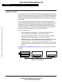
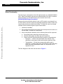
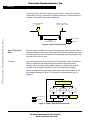
arbitration. Figure 1 shows this concept of communication.
LIN’s main features are:
•
Minimal hardware requirements — Only one bidirectional line of
communication, allowing a baud rate as high as 20 kbps
•
Synchronization frame available — No need for crystals or ceramic
resonators, which is very useful in a low-cost environment
•
Integrated routines — Data checksum in each frame and error detection
in physical layer (bit error) and data link layer (two parity bits)
•
Standard protocol — Based on the standard UART/SCI, which is very
common, allowing easier debugging and a better understanding of the
protocol
See References and Recommended Links for more information on LIN basic
concepts.
MASTER CONTROL UNIT
SLAVE CONTROL UNIT
SLAVE CONTROL UNIT
SLAVE TASK
SLAVE TASK
MASTER TASK
SLAVE TASK
BUS
Figure 1. LIN Concept
Slave LIN Driver for the MC68HC908QT/QY Family
For More Information On This Product,
Go to: www.freescale.com
Freescale Semiconductor, Inc.
AN2503/D
LIN Basic Concepts
Error Detection
The slave must detect these errors:
•
Bit error — When sending data, the data monitored on the bus is
different from the bit value that is sent
•
Checksum error — When receiving data, the sum of the inverted
modulo-256 of received bytes plus the checksum is not 0xFF
•
Identifier parity error — When receiving data, the expected ID parity bits
are not equal to the received ones
Freescale Semiconductor, Inc...
Fault confinement depends on system requirements and is not part of the LIN
specification. The most common procedure for fault confinement is performed
by the master asking for the slave status flags.
LIN Driver Software
Description
Because this LIN driver will be implemented in a very small MCU, there are
several aspects that should be considered when implementing the driver:
•
Small size — Size is dependent on the needs of the application and can
be less than 650 bytes with minimum functionality or less than 1 K and
support the LIN specification.
•
High modularity — Based on the application needs, modules can be
configured to enable or disable LIN functionality such as sleep mode, bit
error checking, and parity checking. As modules are disabled, the code
is reduced without affecting functionality.
•
Flexibility — This driver supports sleep mode specification 1.3 and
earlier versions. It can also be configured to manage IDs in different
ways, so that the user can choose the best option for the application.
•
Easy hardware changes — All I/O pins used can be configured easily to
change according to the application needs.
•
Minimal hardware required — Only one timer channel is used, allowing
the user to use the second one; however, the timer is shared and the
channels can’t be managed simultaneously. If a transceiver isn’t used,
only one pin can be used for input and output (from the timer). If the
transceiver is used, only two general-purpose I/O pins and the one used
by the timer can be used. If sleep mode is enabled, IRQ can be used as
an input, or a regulator will handle this functionality.
Slave LIN Driver for the MC68HC908QT/QY Family
For More Information On This Product,
Go to: www.freescale.com
Freescale Semiconductor, Inc.
AN2503/D
Freescale Semiconductor, Inc...
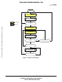
Files Used for LIN
Driver
The files used for the LIN driver are:
•
Source files:
– main.c — Contains driver initialization and the main application
example. See LIN Initialization and Driver Usage and Example.
– slave_drv.c — Contains all the functions available for the driver. See
Driver Functionality for a detailed explanation.
•
Header files:
– slave_drv.h — Contains all the function definitions and macros used
in slave_drv.c.
– lincfg.h — For LIN configuration. See lincfg.h Description.
– linmsgid.h — Contains the defined IDs. See linmsgid.h
Description.
– trimcfg.h — For configuring the trimming process. See Trimming
and trimcfg.h Description.
– resolver.h — Contains buffer definitions used in main program.
– const_table.h — Contains buffers and ROM table definitions.
Figure 2. Files Used for the LIN Driver
Slave LIN Driver for the MC68HC908QT/QY Family
For More Information On This Product,
Go to: www.freescale.com
Freescale Semiconductor, Inc.
AN2503/D
LIN Basic Concepts
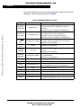
Variables Used in LIN
Driver
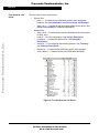
Table 1 provides all the global variables used in this driver and their functions.
Table 1. LIN Driver Variables
Freescale Semiconductor, Inc...
Name
File
Function
*gpMyReceive
main.c
Pointer to a received buffer(1)
*gpMySend
main.c
Pointer to a transmission buffer(1)
gu8PreTrimmed
main.c
Pretrimmed value(2)
gu8CommBuffer[9]
slave_drv.c
I/O Buffer for transfer process
gu8RxShrReg
slave_drv.c
Reception shift register
gu8TxShrReg
slave_drv.c
Transmission shift register
gu8SwScdr
slave_drv.c
Emulated SCI data register
gu8P0
slave_drv.c
General-purpose register
gu8P1
slave_drv.c
General-purpose register
gu8Offset
slave_drv.c
Used to store the trimming offset
gu8IdOrData
slave_drv.c
Defines if arriving byte is ID or data
gu8MsgLength
slave_drv.c
Define expected length for the ID
*gpGeneral
slave_drv.c
Pointer used for transfer purposes
gu8TablePointer
slave_drv.c
Position of ID in ROM table
gu8BitCount
slave_drv.c
Bit counter
gu8InpMode
slave_drv.c
Actual mode of input capture
gu8OverMode
slave_drv.c
Actual mode of overflow
gu8RxErrCounter
slave_drv.c
Reception error counter(3)
gu8TxErrCounter
slave_drv.c
Transmission error counter(3)
gu8ErrReg
slave_drv.c
Error counter
gu8Parity
slave_drv.c
Parity status
gaMsgxxBuffer[ ]
const_table.h
Buffer defined for each ID(3)
gsTableType
.u8ModLength
.*pBufPtr
.u8Id
ROM Table defining all declared vectors
and the following properties:
const_table.h
• Expected length for the ID
• Pointer to the defined buffer
• ID for this table entry
1. Used for example purposes
2. Accessed by slave_drv.c
3. Accessed by main.c
Slave LIN Driver for the MC68HC908QT/QY Family
For More Information On This Product,
Go to: www.freescale.com
Freescale Semiconductor, Inc.
AN2503/D
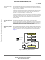
Driver Functionality
The following is a description of the LIN implementation in an MC68HC908QY
MCU. Some functionality may be more understandable if the MCU is familiar.
More information on this MCU and its pinout can be found in the
MC68HC908QY4 Signal Description.
Freescale Semiconductor, Inc...
Because this microcontroller doesn’t have an SCI module, one channel from
the timer will be used as an input and a general-purpose pin will be used as an
output using the timer overflow functionality. To lower the costs, the internal
oscillator can be used through the synch frame feature.
1.
Initialize all variables.
2.
Driver will perform all the functionality in the Interrupt service routines. In
the idle state, it will wait for a new frame.
3.
After a valid break is detected, all the following fields will be expected:
a.
b.
c.
Synch field (where trimming process may occur)
Identifier field (where the slave task will be defined)
Proper action will be executed (either reception or transmission)
• Reception — Waits for the data fields to be defined, store
definitions in the proper buffer and calculate checksum field.
• Transmission — Sends the corresponding buffer and its
checksum. If a sleep mode frame is detected, the MCU will either
enter low power-consumption mode, or it will power off if a
regulator is used.
The flow diagram of the driver can be seen in Figure 3.
6
Slave LIN Driver for the MC68HC908QT/QY Family
For More Information On This Product,
Go to: www.freescale.com
Freescale Semiconductor, Inc.
AN2503/D
Driver Functionality
INT
WAITING_NEWFRAME
RECEIVING_BREAK
INPUT CAPTURE
NO
Freescale Semiconductor, Inc...
OVERFLOW
VALID BREAK
?
YES
SYNCH _RECEPTION
ON_RECEPTION
RECEIVING_DATA
YES
ID OR DATA
?
DATA
BUFFER RECEIVED
?
ID
RX
RECEIVE OR TRANSMIT
?
TX
TRANSMITTING
YES
BUFFER TRANSMITTED
?
NO
Figure 3. LIN Driver Flowchart
Slave LIN Driver for the MC68HC908QT/QY Family
For More Information On This Product,
Go to: www.freescale.com
NO
Freescale Semiconductor, Inc.
AN2503/D
LIN Initialization
Freescale Semiconductor, Inc...
NOTE:
LINInit() function
The main.c file contains the basic structure for initializing this driver based on
the lincfg.h file. Basically the registers that should be configured are:
•
CONFIG1 and CONFIG2 — One-time writable registers used to initialize
various options (internal/external oscillator, enable IRQ, COP
disabled/enabled, etc)
•
OSCTRIM — Specifies the size of the internal capacitor used by the
internal oscillator (changes the oscillator frequency)
•
Variables — All must be initialized to be used in this driver. This
functionality is performed by LINInit() function
In the example, Start08.c doesn’t initialize variables. Therefore, the user must
ensure proper initialization of variables. All variables used by the driver are
properly initialized in code.
This function initializes hardware and variables to a default state.
void LINInit( void )
{
#ifdef TWOPINS
pin*/
SET_OUTPUT_PIN;
#endif /* TWOPINS */
gu8InpMode = WAITING_NEWFRAME;
ChangeTimerConfig(INPCAPTURE);
gu8IdOrData = ID;
#ifdef CHECK_BIT_ERROR
checking */
gu8ErrReg = 0x00;
gu8TxErrCounter = 0x00;
#endif
gu8RxErrCounter = 0x00;
#ifdef ENABLE_TRANSCEIVER
TRANSCEIVER_ENABLE;
#endif
EnableInterrupts;
return;
/* If two pins are defined for I/O, set output
/* Set initial state */
/* Initialize variables used for bit_error
/* Initialize error variables */
}
Error flags are cleared; the transceiver is enabled; the Tx pin is set to a default
state of 1, and the timer is configured for the input capture function in the idle
state of WAITING_NEWFRAME. The timer configuration is performed in the
ChangeTimerConfig() Function.
Slave LIN Driver for the MC68HC908QT/QY Family
For More Information On This Product,
Go to: www.freescale.com
Freescale Semiconductor, Inc.
AN2503/D
Driver Functionality
ChangeTimerConfig()
Function
The ChangeTimerConfig() function is responsible for the timer configuration.
The timer can be configured to function as either input capture or as overflow
using one byte as a parameter.
If the timer is configured as input capture (parameter=0x00), the timer will be
configured to interrupt either with the rising or falling edge if trimming is in
process, or only the falling edges if in any other state.
Freescale Semiconductor, Inc...
If the timer is configured as overflow, the timer pin will be under port control and
the timer will overflow every bit-time. If the internal clock is not fast enough for
a High_Speed LIN, the timer must be configured to overflow sometimes at
one-half bit-time.
WAITING_NEWFRAME
State
After the driver is initialized, it will be waiting in an idle state called
WAITING_NEWFRAME. In this state, the program will wait for bus activity (a
dominant state) which could be the beginning of a new frame. Activity will be
detected by the input capture function of the timer, and the possible break is
validated and jumps to the next state: RECEIVING_BREAK.
RECEIVING_BREAK
State
After a possible break is detected, it should be validated in this state. Basically,
the routine must check whether (during a defined number of bits) the state of
the Rx pin remains low. This is accomplished with the process illustrated in
Figure 4.
WAITING_NEWFRAME
gu8BitCount = 0
INPUT CAPTURE
OVERFLOW
RECEIVING_BREAK
YES
RX = 1
?
NO
gu8BitCount++
NO
gu8BitCount > BREAK_BIT_COUNT
?
YES
SYNCH_RECEPTION
Figure 4. RECEIVING_BREAK Flowchart.
Slave LIN Driver for the MC68HC908QT/QY Family
For More Information On This Product,
Go to: www.freescale.com
Freescale Semiconductor, Inc.
AN2503/D
In this way, the Rx pin will be checked every bit-time. If during one of these
checks the Rx is high, the break is invalid and discarded. The desired timing
diagram for this state can be seen in Figure 5.
Freescale Semiconductor, Inc...
WAITING_NEWFRAME
InpCapt Int
BREAK_BIT_COUNT Int
RX = HIGH, BREAK = VALID
INPUT CAPTURE
RECEIVING_BREAK
OV Int
(RX MUST REMAIN LOW)
OVERFLOW
Figure 5. Break Timing Diagram
Synch_Reception
State
After the break is validated, the next field is the synch field. Because 0x55 is
expected, the MCU will use this field to synchronize with the master timer. If the
external oscillator is used, this process is not necessary and the program must
only wait for this byte to pass.
Trimming
The trimming process is very important in LIN because it allows inexpensive
MCUs to implement LIN using an internal oscillator. Because internal
oscillators are not within an acceptable tolerance by default, they must be
trimmed to an acceptable tolerance in order to communicate properly.
This is accomplished by performing some relative calculations based on the
time elapsed between bit-times. This function is implemented as seen in
Figure 6.
SYNCH_RECEPTION
START
BIT?
3 BIT-TIMES
ELAPSED?
YES
INPUT CAPTURE
GET OFFSET
LAST
BIT?
YES
CALCULATE AND
WRITE NEW TRIM
YES
ON_RECEPTION
OVERFLOW
Figure 6. SYNCH_RECEPTION Flowchart
Slave LIN Driver for the MC68HC908QT/QY Family
For More Information On This Product,
Go to: www.freescale.com
Freescale Semiconductor, Inc.
AN2503/D
Driver Functionality
The calculation of the new trim value is performed using a previously read
offset and the time elapsed in the internal clock during three bit-times, based
on equation 1:
EQUATION 1:
fBus × INT_COUNT
EXPECTED_VAL =
Prescaler × fLIN
WHERE:
fBus IS MCU INTERNAL BUS FREQUENCY
fLIN IS LIN BAUD RATE
INT_COUNT IS NUMBER OF INTERRUPTS TO COUNT TO OBTAIN AN EXPECTED VALUE (IN BIT-TIMES)
Freescale Semiconductor, Inc...
PRESCALER IS TIMER PRESCALER
EXPECTED_VAL IS THE EXPECTED VALUE TO BE READ WHEN INT_COUNT IS REACHED
Because a change in the OSCTRIM register is equal to approximately a 0.2%
change in the internal frequency, equation 2 is derived from equation 1:
EQUATION 2:
1=
fBus(0.002) × INT_COUNT
Prescaler × fLIN
USING:
fBus = 3.2 MHz
fLIN = 9600 bps
THE EXPECTED VALUE FOR
INT_COUNT
Prescaler
IS
3
2
SO: INT_COUNTER = 3
PRESCALER = 2
With these values, every variation from the expected value will represent a
0.2% change in the oscillator and thus a direct (1:1) change in the OSCTRIM
register.
Because EXPECTED_VAL = 500 and the internal oscillator can vary ±25%, the
possible values to be read are:
500 + 25% = 625 (0x271) — Maximum
500 – 25% = 375 (0x177) — Minimum
Consequently, to use only one byte, all values will be added with an offset:
0x271 + 0x89 = 0x2FA — Maximum
0x177 + 0x89 = 0x200 — Minimum
0x1F4 + 0x89 = 0x27D — Expected
In this way, the high byte can be discarded and every change from the
expected value (0x27D) will represent a direct change in the OSCTRIM
register.
Slave LIN Driver for the MC68HC908QT/QY Family
For More Information On This Product,
Go to: www.freescale.com
Freescale Semiconductor, Inc.
AN2503/D
STOP BIT
BIT 0
10
WAIT FOR ID
BIT 1
BIT 2
BIT 3
8
SECOND TRIM
BIT 4
BIT 5
BIT 7
START BIT
SYNCH
DEL
= SYNCH_RECEPTION
InpCapt Ints
Figure 7. SYNCH_RECEPTION Timing Diagram
STOP BIT
BIT 0
BIT 1
BIT 2
BIT 3
BIT 4
After the start bit is detected, the timer is configured to overflow on every
bit-time to capture all eight bits as shown in Figure 8.
BIT 5
RECEIVING_DATA
State
BIT 6
After the synch field is received, the next state will wait for the start bit of the
next field, the identifier field. After the start bit is detected using the input
capture functionality, all the eight bits representing the ID must be received.
This process is performed in the RECEIVING_DATA state.
BIT 7
ONRECEPTION
State
START BIT
Freescale Semiconductor, Inc...
BREAK
BIT 6
5
FIRST TRIM AND
NEW OFFSET
2
GET OFFSET
= RECEIVING_DATA
OV Int
= ON_RECEPTION
InpCapt Int
Figure 8. Byte Reception Timing Diagram
Slave LIN Driver for the MC68HC908QT/QY Family
For More Information On This Product,
Go to: www.freescale.com
Freescale Semiconductor, Inc.
AN2503/D
Driver Functionality
GetChar() Function
After the byte is received, the GetChar() function handles the byte in one of two
ways, depending the byte type.
•
Byte received is an ID — These steps must be performed:
1. The parity error is checked based on a mixed-parity algorithm
2. The ID is validated based on a ROM table and using FindInTable()
function
3. If the ID is defined, the length and direction (transmission or
reception) is obtained
Freescale Semiconductor, Inc...
•
Byte received is data — A previously received ID defined the direction
as reception, and data is received by following these steps:
1. Save the data received in the predetermined buffer
2. If the buffer was received (based on the defined length), the
checksum is calculated using CalcCheckSum() function
3. If the checksum is correct, the buffer is tested to determine if byte is
a SleepMode command.
4. If it is a SleepMode command, the MCU enters low
power-consumption mode.
5. If it is a normal frame, the MCU will wait for the next frame.
This process can be seen in Figure 9.
MOTOROLA
Slave LIN Driver for the MC68HC908QT/QY Family
For More Information On This Product,
Go to: www.freescale.com
Freescale Semiconductor, Inc.
AN2503/D
ON_RECEPTION
RECEIVING_DATA
BIT [7:0]
?
YES
GET BIT
BUFFER
POINTER++
SAVE DATA
BUFFER
RECEIVED?
NO
Freescale Semiconductor, Inc...
IDORDATA =
ID OR DATA?
NO
DATA
YES
ID
CHECK
CHECKSUM
CHECK PARITY BITS
STOP
YES
PARITY OK?
NO
YES
ID DEFINED?
POINT TO BUFFER
CHECKSUM
OK?
YES
NO
SLEEP MODE?
NO
NO
SET ERROR
YES
IDORDATA = DATA
RX
RECEIVE OR
TRANSMIT?
WAITING_NEWFRAME
(TX)
TRANSMIT
Go to
Figure 11
INPUT CAPTURE
OVERFLOW
Figure 9. Reception Process Flowchart
14
Slave LIN Driver for the MC68HC908QT/QY Family
For More Information On This Product,
Go to: www.freescale.com
Freescale Semiconductor, Inc.
AN2503/D
Driver Functionality
FindInTable()
Function
Use this simple look-up function when a small ROM table is defined for space
purposes. The function starts looking for an ID from the bottom of a table to the
first of its elements. It can increase overhead, but it is very useful for code sizing
purposes. Because it is written in assembly, it executes quickly.
FindInTable() function code:
Freescale Semiconductor, Inc...
UINT8 FindInTable(UINT8 temp)
{
asm{
LDA temp
STA gu8P1
LDHX #POINTER_TO_LAST
LDA #LIN_MSGS
LOOP:
PSHA
LDA gu8P1
CMP ,X
BNE NE
PULA
DECA
BRA END
NE:
TXA
SUB #3
TAX
PULA
DBNZA LOOP
LDA #0xFF
END:
STA gu8P1
}
return gu8P1;
}
CalcCheckSum()
Function
This function is used to check the integrity of a frame calculating the checksum
of the buffer using modulo-256 sum. This functionality can be enabled or
disabled in compiler options.
Sample() Function
This function is used when the integrity of data is very important and there is a
lot of noise in the environment. Each bit is sampled four times, obtaining the
most common value in the sample and flagging an error when values obtained
vary from each other. This function is not recommended in most cases because
it increases the code, it is not specified in LIN, and it can increase overhead
(which creates problems with synchronization). The user has the option to
enable it or disable it.
Slave LIN Driver for the MC68HC908QT/QY Family
For More Information On This Product,
Go to: www.freescale.com
Freescale Semiconductor, Inc.
AN2503/D
STOP BIT
BIT 0
BIT 1
BIT 2
BIT 3
BIT 4
BIT 5
BIT 6
BIT 7
START BIT
Transmitting State
= TRANSMITTING
OV Int
Freescale Semiconductor, Inc...
Figure 10. Byte Transmission Timing Diagram
After a byte is sent, the PutChar() function will decide whether another byte
must be sent or the transmission must end. The complete flowchart for LIN
transmission can be seen in Figure 11.
TRANSMIT
POINT TO BUFFER
TRANSMITTING
START
BIT?
BIT[7:0]?
STOP
BIT?
YES
YES
YES
SEND
START BIT
SEND
NEXT BIT
SEND
STOP BIT
BUFFER
AND CHECKSUM
TRANMSITTED?
BUFFER
POINTER++
NO
YES
INPUT CAPTURE
OVERFLOW
WAITING_NEWFRAME
Figure 11. Transmission Process Flowchart
16
Slave LIN Driver for the MC68HC908QT/QY Family
For More Information On This Product,
Go to: www.freescale.com
Freescale Semiconductor, Inc.
AN2503/D
Driver Functionality
Freescale Semiconductor, Inc...
InitializeMsgTransmission() This function initializes the transmission process. It sets all the needed
variables to the proper state, calculates the checksum for the buffer to be sent,
Function
and points to the first element of the buffer.
PutChar() Function
This function controls the transmission flow, either terminating the transmission
(if the last byte was sent) or setting the next byte in the buffer to be sent.
Sleep Mode
Functionality
Sleep mode is compatible with LIN Specification 1.2 and earlier and must be
enabled manually. When a sleep mode command is detected, the MCU will
enter low-consumption mode. The MC68HC908QY MCU uses stop mode,
which stops all activity including timers. This will reduce current consumption
from approximately 4.5 mA to less than 0.22 mA. The MCU will wake up only
with a keyboard interrupt (KBI), an external interrupt (IRQ), or a reset. In this
driver, IRQ is enabled before entering this mode and is the only way to wake
without resetting the MCU. This functionality can be implemented with or
without a transceiver.
If a transceiver is not used, the Rx pin must be tied with the IRQ pin, so that
when a 0 (dominant state) is received, IRQ will be latched and the MCU will
wake up.
If a LIN transceiver is used, there are two options:
Wake Up
•
Use the INH functionality of the MCU connected to IRQ so that it can
wake up.
•
Use a voltage regulator where the INH pin is connected to a shutdown
pin in the regulator and it is turned off. After some bus activity, the
regulator will enable its voltage output and will turn the MCU on. In this
case, the MCU will be reset and proper steps must be taken to avoid
losing information.
The MCU will wake up with an external interrupt or if a reset occurs. If a reset
occurs, the complete driver will be re-initialized and information in buffers will
be lost. In case of an external interrupt, all activity will continue. IRQ will be
disabled until a new sleep mode is detected and the transceiver (if used) will be
enabled.
Slave LIN Driver for the MC68HC908QT/QY Family
For More Information On This Product,
Go to: www.freescale.com
Freescale Semiconductor, Inc.
AN2503/D
Driver Configuration
To provide the required functionality, modularity, and small code size, three
files must be configured with user options. These files contain definitions for
enabling/disabling different functional modules, defining IDs to be used, and
other configuration options. All macros must be configured properly; if the
declaration is not as stated, the driver may not work properly.
Freescale Semiconductor, Inc...
lincfg.h Description
This file is used to configure the LIN driver as needed by the application. Three
main parts can be distinguished:
•
Modular macros — Depending on the options enabled, code and
overhead will increase. Depending on the combination used, the desired
baud rate may not be reached. Table 2 explains all the options available,
the possible values, and the increment in code. The common
implementation of this driver (based on LIN specifications) uses
950 bytes with the following options:
– Includes main.c example.
– Using internal oscillator
– 9600 baud rate
– Rx and Tx pins
– Timer channel 1 is used
– Using a transceiver
– Error checking (bit error, parity and checksum)
– Sleep mode V1.2 enabled
– No quick commands
– Using smaller ROM table with seven IDs defined
All of the code increments shown in Table 2 are based on these arguments,
and they can reduce code as much as 300 bytes, leaving only 655 bytes of
code.
18
•
Constants and media access macros — Options changeable according
to the hardware used and depending on the application. Table 3
explains these options and the possible values.
•
Auto-calculated macros — Defined automatically with modular macros
options and allow the use of bidirectional mode and different channels
from the timer. Table 4 explains all the macros defined here.
Slave LIN Driver for the MC68HC908QT/QY Family
For More Information On This Product,
Go to: www.freescale.com
Freescale Semiconductor, Inc.
AN2503/D
Driver Configuration
.
Table 2. Modules
Functionality
Possible Values
Freescale Semiconductor, Inc...
Size
Increment
INT_OSC
Internal oscillator is used.
Synch field used to trim the internal oscillator.
Very useful to reduce costs.
+0
EXT_OSC
External oscillator is used.
Because no trimming is performed, code is
reduced.
Useful to increment the internal frequency (if a
fast oscillator is used) but more expensive.
–93 bytes
MEDIUM_SPEED
Predefined baud rate for medium LIN speed of
9600 bps.
+0
HIGH_SPEED
Predefined baud rate for high LIN speed of
19200 bps.
Code increments because adjustments must be
made to accomplish this baud rate.
+18 bytes
SLOW_SPEED
Predefined baud rate for slow LIN speed of
2400 bps.
Code increments because adjustments must be
made to accomplish this baud rate.
+12 bytes
One Pin
Timer channel pin used is used as Rx and Tx.
Useful when testing with a CPU serial port using
only one line (using the same PTA0 used for
MON08 communication).
+0
Two Pins
Timer channel pin is used as Rx pin only and a
general-purpose pin is used as Tx only.
Used more often because it accommodates
transceivers.
+0
TIMER_USED_1
Timer channel 1 (PTA1) is used as Rx.
Very useful when used with MON08 because
PTA0 can be used at the same time for monitor
mode communication.
Ensure that it has a high value when entering
monitor mode.
+0
TIMER_USED_0
Timer channel 0 (PTA0) is used as RX.
Very useful when the same line for monitor mode
is used for testing with a CPU serial port.
Monitor mode can be used for programming
purposes only, not for debugging.
+0
ENABLE_TRANSCEIVER
Transceiver is used.
It must be properly enabled/disabled
+0
DISABLE_TRANSCEIVER
Transceiver is not used.
Useful for testing purposes with a CPU.
Oscillator
Mode
LIN Baud Rate
Number of
Pins Used
Timer Used as
Rx
Use of
Transceiver
Description
Slave LIN Driver for the MC68HC908QT/QY Family
For More Information On This Product,
Go to: www.freescale.com
–10 bytes
Freescale Semiconductor, Inc.
AN2503/D
Table 2. Modules (Continued)
Functionality
Possible Values
Description
Bit error (defined in LIN specification)(1) is
checked.
Useful for LIN specification compliance.
CHECK_BIT_ERROR
Bit Error
Checking
NO_CHECK_BIT_ERROR
Bit error is not checked. The Tx pin will transmit
regardless of what it reads.
Useful when this error is not important or when
the master can handle it properly.
Size
Increment
+0
–60 bytes
Freescale Semiconductor, Inc...
1. For a link to the complete LIN specification, see References and Recommended Links.
Table 3. Modular Macros in lincfg.h
Functionality
Possible Values
PARITY_ERROR
Parity Error
Checking
20
Parity error (defined in LIN specification)(1) is
checked.
Useful for LIN specification compliance.
Size
Increment
+0
NO_PARITY_ERROR
Parity error not checked.
Useful when checksum is sufficient to check data
integrity or if the master can handle a possible
error.
–95 bytes
MULTI_SAMPLE
Multi sample is enabled. Four samples are
performed when reading data from Rx.
Useful when noise may be an issue.
Not recommended because of the overhead, and
it can cause the LIN driver to fail if the oscillator
is too slow and the baud rate is high.
+34 byes
NO_MULTI_SAMPLE
Single sample. Only one sample is taken from Rx.
Useful most of the time and can be enough for
most applications. LIN specification does not
state how data must be sampled.
+0 bytes
DISABLE_SLEEP
Sleep mode is disabled. Used when there is no
need to enter low power-consumption mode.
–46 bytes
ENABLE_SLEEP_1_0
Sleep mode (LIN versions earlier than V1.2) is
enabled. ID is 0x00.
–2 bytes
ENABLE_SLEEP_1_2
Sleep mode (LIN V1.2) is enabled. ID is 0x3C and
first data is 0x00.
Multi Sample
on RX
Sleep Mode
Description
Slave LIN Driver for the MC68HC908QT/QY Family
For More Information On This Product,
Go to: www.freescale.com
+0
Freescale Semiconductor, Inc.
AN2503/D
Driver Configuration
Table 3. Modular Macros in lincfg.h (Continued)
Functionality
Freescale Semiconductor, Inc...
Enable Quick
Commands
Possible Values
QUICK_COMMAND
Description
Size
Increment
Quick commands are enabled. A function named
QuickAction() is performed immediately after
+4 bytes
receiving a new frame, which allows for
+QuickAction()
immediate action to be taken. If QuickAction() is
function
too big, the next frame can be lost.
NO_QUICK_COMMAND
After receiving a new frame, it is only written to its
buffer and user must handle it properly.
+0
SMALLER_TABLE
A smaller ROM table is defined in ROM memory.
Useful when there are few IDs defined because
code is smaller, but it will increase overhead
because of a look-up table function.
Do not use if there are too many IDs defined.
+3 bytes per
extra ID
(lookup
function uses
40 bytes)
ROM Table
Used
FASTER_TABLE
A complete ROM table is defined in ROM memory
+128 bytes
with all IDs defined in a vector.
non-dependan
Useful when there are too many IDs defined and a
t of IDs.
look-up table is not needed, and when overhead
(–14 used in 7
must be reduced. However it will increase the
IDs example)
code substantially.
1. For the complete LIN Specification, see References and Recommended Links.
Slave LIN Driver for the MC68HC908QT/QY Family
For More Information On This Product,
Go to: www.freescale.com
Freescale Semiconductor, Inc.
AN2503/D
Freescale Semiconductor, Inc...
Table 4. Constants and Media Access Macros in lincfg.h
Constant
Possible
Values
BREAK_BIT_COUNT
Unsigned
8 bits
PRE_TRIMMED_VALUE
Optional
or unsigned
8 bits
Pre-trimmed value from factory to load into OSCTRIM register.
Use optional if this register (20xFFC0) has a pre-trimmed value
from factory.
If this value was erased, write your own using any unsigned 8-bit
value.
SET_OUTPUT_PIN
Set Tx high
When two pins are used, Tx must be as an output high when
initializing LIN. This macro must set this condition.
TWOPINS_TX_HIGH
PTx_PTxx=1
Used to set Tx in high state.
Ensure that the Tx pin is mapped here.
TWOPINS_TX_LOW
PTx_PTxx=0
Used to set Tx in low state.
Ensure that the Tx pin is mapped here.
TRANSCEIVER_ENABLE
Set
transceiver
EN pin high
If a transceiver is used, this macro enables the transceiver when
LIN is initialized.
Ensure that the pin connected to the transceiver’s EN pin is
mapped here.
TRANSCEIVER_DISABLE
Set
transceiver
EN pin low
If a transceiver is used, this macro disables the transceiver when
LIN is initialized.
Ensure that the pin connected to the transceiver’s EN pin is
mapped here.
LIN_BAUDRATE
A LIN
baud rate
This macro is obtained automatically based on the LIN baud rate
defined.
To use a different baud rate, see trimcfg.h Description
MCU_Fbus (fBus)
MCU internal
operating
frequency
22
Description
Number of bit counts in order to recognize a valid break.
This macro is obtained automatically based on the oscillator
mode used.
fBus must remain the same, but the external frequency can
change according to the external oscillator used.
Slave LIN Driver for the MC68HC908QT/QY Family
For More Information On This Product,
Go to: www.freescale.com
Freescale Semiconductor, Inc.
AN2503/D
Driver Configuration
Table 5. Auto Calculated Macros In lincfg.h
Macro
Description
TSCCHREG
TSCCHF
TIM_CH_INT_VECTOR
ACK_INPCAPTUREINT_CH
Freescale Semiconductor, Inc...
TCHLREG
trimcfg.h
Description
Timer channel control register
Timer channel overflow flag
Timer channel interrupt vector
Timer channel interrupt acknowledge
Timer channel low register
ONEPIN_TX_HIGH
Set high Tx output pin if using bidirectional mode
ONEPIN_TX_LOW
Set low Tx output pin if using bidirectional mode
is_RX_HIGH
Check whether Rx pin is high
is_RX_LOW
Check whether Rx pin is low
SET_TX_HIGH
Set Tx pin high
SET_TX_LOW
Set Tx pin low
This file is used to define all macros and constants used for the trimming
process defined in Trimming. The definitions used here are calculated for the
recommended bit rates for LIN. If the baud rate will be changed, the user must
configure this file properly including according to the section above.
All the constants declared in this file can be seen in Table 6 with a brief
description.
Table 6. Constants Defined in trimcfg.h
Macro
VARIATION
START_BIT_COUNT
Description
Allowed variation for internal oscillator.
Defined by user.
Number of bit counts for the start bit.
TRIM1_COUNT
Number of bit counts to wait for the first trim
calculation.
TRIM2_COUNT
Number of bit counts to wait for the second trim
calculation.
STOP_BIT_COUNT
Number of bit counts for the stop bit.
INT_COUNT
Number of bit counts elapsed from offset to trim
calculation.
PRESCALER
Timer prescaler to perform a correct trimming.
PS_VALUE
Value loaded into timer control register to set
prescaler. Prescaler = 2 PS_VALUE.
EXPECTED_VAL
Expected value to be read if the internal clock is
3.2 MHz.
Slave LIN Driver for the MC68HC908QT/QY Family
For More Information On This Product,
Go to: www.freescale.com
Freescale Semiconductor, Inc.
AN2503/D
Table 6. Constants Defined in trimcfg.h (Continued)
Freescale Semiconductor, Inc...
Macro
linmsgid.h
Description
Description
MAX_VALUE
Maximum possible value to be read
(3.2 MHz + 25%).
MIN_VALUE
Minimum possible value to be read
(3.2 MHz – 25%).
u8_TO_SCALE
Value to be added in order to use only chars and
discard the high byte.
u8_MID_EXPECTED
Expected scaled value.
Compared with the read value to check variation.
u8_MAX_EXPECTED
Maximum allowed value based on the variation
defined.
u8_MIN_EXPECTED
Minimum allowed value based on the variation
defined.
Use this file to define all the valid identifier fields and their functions. Code size
depends on the number of IDs defined. These IDs and the total number of IDs
used must be defined correctly to ensure proper functionality of the LIN driver.
If the application requires the use of many IDs, use the FASTER_TABLE
definition described in Table 3. This is recommended because the ROM table
will remain the same and the FindInTable() function will not be used, reducing
the overhead. If SMALLER_TABLE definition is used, the code will be smaller
and the FindInTable() function will look up the ID(s) in the ROM table. In this
case, each ID defined will increase code size by four bytes.
The ID definition must follow these steps:
1.
Define the location of ROM table in MESSAGES_ROM_ADDRESS
constant.
2.
Define number of IDs to use (including reserved commands if used) in
LIN_MSGS.
3.
Comment or erase all the unused IDs and define the ones to be used.
LIN_MSG_xx must contain the direction of the ID and
LIN_MSG_xx_LEN must contain the data length(1)
Table 7 shows all the constants used in this file.
24
Slave LIN Driver for the MC68HC908QT/QY Family
For More Information On This Product,
Go to: www.freescale.com
Freescale Semiconductor, Inc.
AN2503/D
Hardware Implementation
Table 7. Constants Defined in linmsgid.h
Macro
MESSAGES_ROM_ADDRESS
Freescale Semiconductor, Inc...
LIN_MSGS
Description
Start address for the ROM table (16 bits).
Number of IDs defined (1 to 64 bits).
LIN_MSG_xx(1)
Direction of ID:
LIN_RECEIVE — Data will be received in the
buffer when an ID arrives.
LIN_SEND — Data in buffer will be sent when an
ID arrives.
LIN_MSG_xx_LEN(1)
Length of data (buffer) to be received. (1–8 bits)
POINTER_TO_LAST
Auto-calculated pointer points to the last ID in
ROM table.
Do not change.
1. Where xx is the ID number in hexadecimal format
Hardware Implementation
This LIN driver is intended to be flexible with user hardware. This
demonstration is implemented in MC68HC908QY4 slave LINkit hardware (see
Schematic).
MC68HC908QY4
Signal Description
The main features of the MC68HC908QY4 MCU are:
•
4 K of FLASH memory (1.5 K in the MC68HC908QY1/QY2)
•
128 bytes of RAM memory
•
No SCI module
•
Some pins share functionality (ADC, TIM, KBI, OSC, IRQ, and RST).
•
One timer with two channels (TIMCH0 and TIMCH1)
•
Timer has input capture, output compare and overflow functionality.
•
External interrupt (IRQ) available at PTA2.
•
Reset (RST) available at PTA3, not enabled by default.
•
Oscillator (OSC) pins available at PTA4/PTA5.
•
One general-purpose only 8-bit port (PTB).
•
PTA0 (TIMCH0) is used to enter monitor mode and program the MCU.
•
PTA1 (TIMCH1) must be tied high when entering monitor mode.
•
Internal oscillator available; external oscillator can be used.
•
Internal frequency using internal oscillator is 3.2 MHz ±5% before
trimming.
Slave LIN Driver for the MC68HC908QT/QY Family
For More Information On This Product,
Go to: www.freescale.com
Freescale Semiconductor, Inc.
AN2503/D
The driver is designed to use as few pins as possible to reserve some for the
application. The pin usage is described in Table 8.
Table 8. MC68HC908QY4 Pin Usage
Pin
Freescale Semiconductor, Inc...
Comments
MON08 Comm
Used for programming/debugging. Can be used to
test driver with CPU in bidirectional mode (no
debug).
One timer channel is available in real application.
PTA1/AD1/
TCH1/KBI1
LIN reception (Rx)
Must be tied to VDD when entering monitor mode
(disconnect when using a transceiver).
Reception only when using the transceiver.
One timer channel is available in real application.
PTA2/IRQ/
KBI2
Programming voltage
PTA3/RST/
KBI3
Reset
PTA4/OSC2/
AD2/KBI4
Not used
Must be tied to GND/VSS when entering monitor
mode.
Available in real application.
PTA5/OSC1/
AD3/KBI5
9.8304 MHz oscillator.
Used for programming. Can be used instead of
internal oscillator.
Available in real application.
PTB0
Push button
Available in real application.
PTB1
Not used
Available in real application.
PTB2
LIN transmission (Tx)
PTB3
LED
Available in real application.
PTB4
LED
Available in real application.
PTB5
LED
Available in real application.
PTB6
LED
Available in real application.
PTB7
LIN transceiver enable
PTA0/AD0/
TCH0/KBI0
26
Use
Used for programming only. Can be used to wake up
the MCU without a regulator (not in this board).
Available in real application.
Available in real application.
One general-purpose pin for transmission is needed
in real application when using a transceiver.
One general-purpose pin to enable the transceiver is
needed in real application when using a transceiver.
Slave LIN Driver for the MC68HC908QT/QY Family
For More Information On This Product,
Go to: www.freescale.com
Freescale Semiconductor, Inc.
AN2503/D
Hardware Implementation
Another important component in the board is the MC33399, the LIN
transceiver. This transceiver is a physical layer component dedicated to
automotive sub-bus applications. It is compliant with LIN specifications, sleep
mode, and wake up capability. The transceiver can wake up from sleep mode
with three different events:
MC33399
Description
•
Wake-up signal from the wake pin
•
Active signal in EN pin
•
LIN bus activity
Freescale Semiconductor, Inc...
The last two events will be used in this board. The pin description for this
transceiver can be found in Table 9.
Table 9. MC33399 Pin Usage
Pin
Description
Rx
LIN reception
EN
Transceiver enable
WAKE
Wake input
Tx
LIN reception
GND
Ground
Provides ground (VSS).
LIN
LIN bus
The single-wire bus transmitter
and receiver.
VSUP
Power supply
INH
Inhibit
Use
Connection
Reports the state of the LIN bus
voltage.
PTA1 in
MC68HC908QY4
Controls the operation mode
(active or sleep).
PTB7 in
MC68HC908QY4
High-voltage input used to wake
the device from sleep mode.
MCU interface that controls the
state of the LIN output.
Provides power supply (7 to 27 V).
Used in this board to control an
external switchable voltage
regulator. Can be negated and
used as an external interrupt to
wake the MCU.
GND
PTB2 in
MC68HC908QY4
GND
Pin 4 of connector
LIN MOLEX
VSUP
SHDN pin in
regulator
Voltage Regulator
This board also includes a voltage regulator with shutdown capability which
supplies all the circuitry, excluding the LIN transceiver. This will enable the
transceiver to wake all the components when LIN bus activity is detected.
Headers, Jumpers,
and Connectors
This board allows for direct connectivity with a LIN bus, at the same time
allowing programming and debugging capabilities. This is accomplished by the
jumpers described in Table 10.
Slave LIN Driver for the MC68HC908QT/QY Family
For More Information On This Product,
Go to: www.freescale.com
Freescale Semiconductor, Inc.
AN2503/D
Table 10. Jumper Description
Jumper
J2
J3
Freescale Semiconductor, Inc...
J4
J5
Symbol
Description
IRQ with pullup to VDD
IRQ connected to Vtst (to program the MCU)
PTA1 with pullup to VDD (used to enter monitor mode)
PTA1 connected to Rx pin
Debug circuitry off (OSC and RS-232 Transceiver)
Debug circuitry supplied to VDD
9.8304 MHz OSC disconnected
9.8304 MHz OSC connected to OSC1 (to program the MCU)
There are also two connectors (CON1 and CON2) to connect the board directly
to a LIN bus. Their pinouts can be found in Table 11.
Table 11. LIN Connectors CON1 and CON2
28
PIN
Description
1
VSS
2
VSS
3
VSUP
4
LIN
5
VSS
6
VSS
Slave LIN Driver for the MC68HC908QT/QY Family
For More Information On This Product,
Go to: www.freescale.com
Freescale Semiconductor, Inc.
AN2503/D
Schematic
Schematic
~12 V
VBat
8
1
LT1121
5V
3
5
100 kΩ
47 kΩ
100 kΩ
2.2 kΩ
1 kΩ
100 nF
Freescale Semiconductor, Inc...
J2
(MONITOR
MODE)
27 kΩ
LIN
6
7
VSup
8
INH
LIN
MC33399
3 WAKE
5
VDD
J4
13
5 V (DEBUG)
47 kΩ
6
Rx 1
16
GND
5
J3
15
B7
3
PUSH-BUTTON
S1
MC68HC908QY4
A1 (Rx)
14
B3
11
B4
10
B5
7
B6
B2 (Tx)
OSCILLATOR MODULE
8
(DEBUG)
OSC1
J5
10 kΩ
B0
IRQ
RESET
9.1 V
ZENER
EN 2
Tx 4
12
RESET
VSS
4
1 kΩ 1 kΩ 1 kΩ 1 kΩ
GND
Driver Usage and Example
This section shows how to implement the driver with reference to the example
project, AN2503SW. This file can be downloaded from the Freescale LIN
website, http://freescale.com
Configure lincfg.h
Write lincfg.h according to the implementation needs. Review lincfg.h
Description for a complete description of this file. In the AN2503SW, the driver
is configured as described below:
•
•
•
•
•
•
•
•
Internal oscillator used
Medium 9600 bps LIN frequency (fLIN) used
PTA0 used as bidirectional pin for communication
Transceiver is not used
Bit error and parity error are checked/enabled
QuickAction commands are not used
Smaller ROM table is defined
Trimmed value of 0x19 is used
Slave LIN Driver for the MC68HC908QT/QY Family
For More Information On This Product,
Go to: www.freescale.com
Freescale Semiconductor, Inc.
AN2503/D
Modify trimcfg.h
Modify this file according to the needs of the application. Review trimcfg.h
Description for a complete description on this file. In this example, the normal
implementation for 9600 bps is used.
Configure
linmsgid.h
This file must include the definition of all the IDs used in the application. Review
linmsgid.h Description for using this file. In this example, the following IDs are
defined:
Freescale Semiconductor, Inc...
Table 12. Example ID Definitions
Write main()
ID
Mode
Length
0x00
Reception
2
0x1A
Reception
8
0x1B
Transmission
8
0x1C
Reception
4
0x1D
Transmission
2
0x1E
Transmission
2
0x3C
Reception
8
The main files already include the definition for configuration registers and LIN
peripherals, but they can be changed by the user if the application requires it.
LIN is a one-master/multi-slave protocol, and slaves can’t participate on the
bus until they are required to. The buffers are updated in the interrupts, and it’s
the user’s responsibility to ensure their proper use. The main file for
AN2503SW contains an example of LIN use. Also, keep in mind that any
defined buffer can be accessed directly — including the resolver.h file. Any
access to the buffers can be direct or indirect (through the use of pointers) to
help increase readability.
In AN2503SW, the example sends with ID 0x1B. The first five bytes of the
buffer receives ID 0x1A and two error counters (one for reception and one for
transmission).
Notice that the sixth element is undefined. Because the buffer isn’t initialized,
the value will be undefined with the actual RAM value.
30
Slave LIN Driver for the MC68HC908QT/QY Family
For More Information On This Product,
Go to: www.freescale.com
Freescale Semiconductor, Inc.
Freescale Semiconductor, Inc...
AN2503/D
Driver Usage and Example
Write QuickAction()
This function is included in slave_drv.c, and it’s the only function changeable
by the user in a normal application. Use this function when an action must be
performed immediately after the ID is received. Remember that functions
included in this part must not be extensive unless the LIN master guarantees
enough time between LIN transfers. An extensive function can result in an
undesired lost of frame. In AN2503SW, the pin PTB3 is toggled every time the
ID 0x1A is received with a value of 0x00 in the first byte. However, this function
is not defined because the QUICK_COMMAND definition is not used.
Compile and
Download Your
Application
Check for any errors in compilation and download your application to the MCU.
Remember that the MCU must enter monitor mode and some signals are
required:
•
PTA0 for MON08 communication
•
PTA1 tied to VDD
•
PTA4 tied to GND
•
IRQ tied to Vtst
Any change in these signals could result in programming errors. Check the
board jumpers.
Test Your
Application
There are several ways to test and debug your application depending on the
application:
•
A computer program can be easily implemented to test your IDs and the
response of the MCU.
•
If the project is in development or for a quicker design without using a
transceiver, use PTA0 as bidirectional line and test it with the same
hardware used for programming the PC.
•
A simple transceiver with an RS-232 to a TTL converter can help you to
use your PC as a LIN master.
•
The LIN frames are very easy to see and recognize with the aid of an
oscilloscope.
Slave LIN Driver for the MC68HC908QT/QY Family
For More Information On This Product,
Go to: www.freescale.com
Freescale Semiconductor, Inc.
AN2503/D
LIN Driver Features and Performance Comparison
Freescale Semiconductor, Inc...
The Freescale LIN website contains application notes and drivers for different
implementations. So, you can find the design that best matches your
application. Some influential factors affecting your MCU decision could include:
•
Master/Slave tasks or only slave tasks
•
Memory requirements
•
Number of available pins
•
Other physical interfaces (SPI, IIC, LCD, etc.)
•
Development time
•
Cost
The application described in this documents is intended to cover the
lowest-end part of the LIN portfolio, meaning:
32
•
Only slave tasks — This driver implements only slave tasks, meaning
that the node must be a slave, executing commands and sending data
only by master requests.
•
Low memory requirements — This driver is intended to be used in a
member of the MC68HC908QT/QY Family, whose members have 1.5K
and 4K FLASH. This driver uses approximately between 600 bytes to
1K, allowing the user to implement the driver in the smallest MCU from
Freescale with enough space for a small application.
•
Low number of available pins — This family has members with 8 pins
(6 I/O) or 16 pins (14 I/O), and the driver can use as few as 1 to 4 pins.
•
No physical interfaces — This family is a low-level general-purpose
family, so it doesn’t include any special distinctive feature, except the
ADC pins and the internal modules.
•
Decreases development time — There are several hardware options
for a LIN implementation including (from simplest to most complex): the
SLIC (slave LIN interface controller), ESCI (enhanced serial
communication interface), SCI (serial communication interface), and
bit-banged timer. However, this driver is intended to reduce the
development time because the user doesn’t have to worry about the
implementation, only to develop his or her own code.
•
Lowest cost — The most important feature about this driver is that it
allows a LIN implementation in the least expensive and smallest
Freescale MCU.
Slave LIN Driver for the MC68HC908QT/QY Family
For More Information On This Product,
Go to: www.freescale.com
Freescale Semiconductor, Inc.
AN2503/D
LIN Driver Features and Performance Comparison
•
Use of API — This application note doesn’t use an API. This represents
an incompatibility with some other application notes, but it reduces the
CPU use and the amount of memory used. It’s a good option to leave
more free memory for the user program.
•
Memory usage — Table 13 shows a comparison between different
implementations of LIN drivers in other available application notes.
•
CPU time and performance — Table 14 shows the differences
between the CPU time and performance in different MCUs and
application notes.
ESCI
TIM08
Table 13. Driver Performance Metrics
SLIC
Freescale Semiconductor, Inc...
Other distinctive features of this application note that the user must consider:
Version
Std
API
Feature
Level
QY/QT bit-banged
drivers
AN2503/D(1)
N
QY/QT bit-banged
drivers
AN2599/D
Y
—
EY16 ESCI
drivers
AN2575/D(2)
Y
LINQL4-ASM
Driver Code Resource Required
ROM (Bytes)
Stack
(Bytes)
536 (+ 3 per msg)
22
836 (+ 3 per msg)
22
32 (+12 per 8 byte
msg)
1103 (driver)
487 (API)
35
—
19 (+1 per 8 byte
msg)
1130
(driver + API)
< 25
N
—
11
(+ 8 per 8 byte msg)
172
7
LINQL4-C
N
—
18
(+ 8 per 8 byte msg)
120
20
LINQL4-API
Y
—
32
(+ 12 per 8 byte msg)
838 (driver)
420 (API)
35
MIN
MAX
RAM (Bytes)
24 (+ 8 per 8 byte
msg)
1. AN2503/D driver assumptions:
MIN = external OSC, 9600bps, no SLEEP mode, no parity check, no bit error checking
MAX = internal OSC, 19200bps, SLEEP, parity checking, and bit error checking enabled
Each also has 7 messages defined, using 26 bytes of RAM
2. AN2575/D memory usage data comes from LIN08 driver manual for EY16.
Slave LIN Driver for the MC68HC908QT/QY Family
For More Information On This Product,
Go to: www.freescale.com
Freescale Semiconductor, Inc.
AN2503/D
Table 14. Driver Performance Metrics
Version
N
AN2503/D
ESCI +
TIM08
No. of
Interrupts/
Msg Frame
(8-byte msg)
Rx(3)
111
120 Tx
LIN Bus
Speed
CPU Speed
(MHz)
Y
EY16 ESCI
drivers
N
97 Rx
106 Tx
LINQL4-ASM
AN2633/D
LINQL4-C
AN2633/D
LINQL4-API
AN2633/D
(2)
19,230
29% (rx)
40% (tx)
9,615
20% (rx)
20% (tx)
19,230
38% (rx)
44% (tx)
9,615
2% (rx)
4% (tx)
19,230
3.2(4)
(calculated)
4% (rx)
7% (tx)
9,615
0.3 (rx)
0.2 (tx)
19,230
0.5 (rx)
0.5 (tx)
9,615
0.4 (rx)
0.4 (tx)
N
N
Average
14% (rx)
20% (tx)
12
AN2575/D
CPU Usage(1)
9,615
3.2
QY/QT bit-banged
drivers
AN2599/D
SLIC
Freescale Semiconductor, Inc...
TIM08
QY/QT bit-banged
drivers
Std
API
2
3.2
19,230
0.8 (rx)
0.8 (tx)
9,615
0.8 (rx)
0.8 (tx)
19,230
1.6 (rx)
1.7 (tx)
Y
Peak
193 µs
272 µs
39 µs
34 µs
61 µs
123 µs
1. CPU usage represents the time spent in the communication ISR(s) vs. time spent doing other tasks. API functions and
handling performed outside of the ISR(s) is not counted against this metric. Average value is reported as a percentage of
times, but is still a function of CPU speed, as LIN communications is asynchronous to CPU operations. CPU usage
numbers are approximate. Peak time represents the longest single interrupt which that be processed.
2. From LIN08 Driver User's Manual: CPU performance is calculated as: L = T active / T frame * 100%
where:
- L is the CPU load in percent;
- T active is the amount of CPU time expended in executing the driver code during T frame;
- T frame is the amount of time required to transmit or receive a regular LIN bus frame of maximum length, containing
8 bytes of data (124 bits). The required LIN message budget of 40% is also taken into account. For Reference: T frame
(9615 bps) = 18.055 ms; T frame (19230 bps) = 9.028 ms.
3. For received data (command) messages, 0x55 data and checksum used for worst case ISR load.
4. EY16 CPU usage information was measured based on 4.9152 MHz CPU frequency, then recalculated for a 3.2 MHz CPU
frequency.
34
Slave LIN Driver for the MC68HC908QT/QY Family
For More Information On This Product,
Go to: www.freescale.com
Freescale Semiconductor, Inc.
AN2503/D
LIN Driver Features and Performance Comparison
Freescale offers a complete portfolio for LIN applications. This allows the user
to choose the best options according to the particular application—from the
lowest end MC68HC908QT/QY design with low CPU, memory, and pin
requirements, to a higher performance MC69HC908QL design with dedicated
hardware and more available CPU and memory for the user. The options
extend to higher requirements and master nodes, including some high-end
HC08 members and some 16-bit families like the HCS12.
Freescale Semiconductor, Inc...
AN2503 is a low-end driver oriented to small, non-intensive applications for
users needing flexibility, optional features, time predictability for all messages
and most of all, very low cost.
Slave LIN Driver for the MC68HC908QT/QY Family
For More Information On This Product,
Go to: www.freescale.com
Freescale Semiconductor, Inc.
AN2503/D
References and Recommended Links
Links
LIN consortium web page
www.lin-subbus.org
Freescale Semiconductor, Inc...
Freescale semiconductors main page
www.freescale.com
Freescale LIN (including products, documentation, and applications)
www.freescale.com
Software
AN2503SW: Driver code source described in this document
Documents
MC68HC908QY4/D: Q Family data sheet
AN2103/D: Local Interconnect Network (LIN) Demo
AN2205/D: Car Door Keypad Using LIN
AN2264/D: LIN Node Temperature Display
AN2343/D: HC908EY16 LIN Monitor
AN2342/D: LIN Sample Application for the MC68HC908EY16
AN2470/D: MC68HC908EY16 Controller Robot Using the LIN Bus
AN2573/D: LIN Kits LIN Evaluation Boards
AN2575/D: MC68HC908EY16 ESCI LIN Drivers
AN2302/D: EEPROM Emulation for the MC9S12C32
AN2344/D: HC908EY16 EMI Radiated Emissions Results
AN2346/D: EEPROM Emulation using FLASH in MC68HC908QY/QT
AN2498/D: Initial trimming of the MC68HC908 ICG
AN2560/D: MC68HC908EY16 IR Receiver for Remote Control of LIN Robot
AN2575/D: MC68HC908EY16 ESCI LIN Drivers
AN2599/D: Generic LIN Driver for MC68HC908QY4
AN2633/D: LIN Drivers for SLIC Module on the MC68HC908QL4
36
Slave LIN Driver for the MC68HC908QT/QY Family
For More Information On This Product,
Go to: www.freescale.com
Freescale Semiconductor, Inc.
Freescale Semiconductor, Inc...
AN2503/D
References and Recommended Links
Slave LIN Driver for the MC68HC908QT/QY Family
For More Information On This Product,
Go to: www.freescale.com
Freescale Semiconductor, Inc.
Freescale Semiconductor, Inc...
AN2503/D
38
Slave LIN Driver for the MC68HC908QT/QY Family
For More Information On This Product,
Go to: www.freescale.com
Freescale Semiconductor, Inc.
Freescale Semiconductor, Inc...
AN2503/D
References and Recommended Links
Slave LIN Driver for the MC68HC908QT/QY Family
For More Information On This Product,
Go to: www.freescale.com
Freescale Semiconductor, Inc.
How to Reach Us:
Home Page:
www.freescale.com
Freescale Semiconductor, Inc...
E-mail:
[email protected]
USA/Europe or Locations Not Listed:
Freescale Semiconductor
Technical Information Center, CH370
1300 N. Alma School Road
Chandler, Arizona 85224
+1-800-521-6274 or +1-480-768-2130
[email protected]
Europe, Middle East, and Africa:
Freescale Halbleiter Deutschland GmbH
Technical Information Center
Schatzbogen 7
81829 Muenchen, Germany
+44 1296 380 456 (English)
+46 8 52200080 (English)
+49 89 92103 559 (German)
+33 1 69 35 48 48 (French)
[email protected]
Japan:
Freescale Semiconductor Japan Ltd.
Headquarters
ARCO Tower 15F
1-8-1, Shimo-Meguro, Meguro-ku,
Tokyo 153-0064
Japan
0120 191014 or +81 3 5437 9125
[email protected]
Asia/Pacific:
Freescale Semiconductor Hong Kong Ltd.
Technical Information Center
2 Dai King Street
Tai Po Industrial Estate
Tai Po, N.T., Hong Kong
+800 2666 8080
[email protected]
For Literature Requests Only:
Freescale Semiconductor Literature Distribution Center
P.O. Box 5405
Denver, Colorado 80217
1-800-441-2447 or 303-675-2140
Fax: 303-675-2150
[email protected]
Information in this document is provided solely to enable system and software
implementers to use Freescale Semiconductor products. There are no express or
implied copyright licenses granted hereunder to design or fabricate any integrated
circuits or integrated circuits based on the information in this document.
Freescale Semiconductor reserves the right to make changes without further notice to
any products herein. Freescale Semiconductor makes no warranty, representation or
guarantee regarding the suitability of its products for any particular purpose, nor does
Freescale Semiconductor assume any liability arising out of the application or use of
any product or circuit, and specifically disclaims any and all liability, including without
limitation consequential or incidental damages. “Typical” parameters which may be
provided in Freescale Semiconductor data sheets and/or specifications can and do
vary in different applications and actual performance may vary over time. All operating
parameters, including “Typicals” must be validated for each customer application by
customer’s technical experts. Freescale Semiconductor does not convey any license
under its patent rights nor the rights of others. Freescale Semiconductor products are
not designed, intended, or authorized for use as components in systems intended for
surgical implant into the body, or other applications intended to support or sustain life,
or for any other application in which the failure of the Freescale Semiconductor product
could create a situation where personal injury or death may occur. Should Buyer
purchase or use Freescale Semiconductor products for any such unintended or
unauthorized application, Buyer shall indemnify and hold Freescale Semiconductor
and its officers, employees, subsidiaries, affiliates, and distributors harmless against all
claims, costs, damages, and expenses, and reasonable attorney fees arising out of,
directly or indirectly, any claim of personal injury or death associated with such
unintended or unauthorized use, even if such claim alleges that Freescale
Semiconductor was negligent regarding the design or manufacture of the part.
AN2503/D
For More Information On This Product,
Go to: www.freescale.com