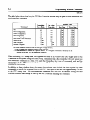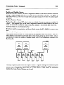
1
GE Fanuc Automation
Programmable
Control Products
.
Series
Bus Controller
User’s Manual
Six'"
GFK-0171B
July, 1991
GFL-002
WARNINGS, CAUTIONS, AND NOTES AS USED IN THIS PUBLICATION
/ WARNING
/
Warning notices are used in this publication to emphasize that hazardous voltages, currents, temperatures,
or other conditions that could cause personal injury exist in this equipment or may be associated with its
use.
In situations where inattention could cause either personal injury or damage to equipment, a Warning
notice is used
CAUTION
Caution notices are used where equipment might be damaged if care is not taken.
NOTE
Notes merely call attention to information that is especklly significant to understanding and operating the
equipment.
This document is based on information available at the time of its publication. While efforts have been made to be accurate,
the information contained herein does not purport to cover all details or variations in hardware and software, nor to provide
for every possible contingency in connection with instalktion, operation, and maintenance. Features may be described herein
which are not present in all hardware and software systems. GE Fanuc Automation assumes no obligation of notice to
holders of this document with respect to changes subsequently made.
GE Fanuc Automation makes no representation or warranty, expressed, implied, or statutory with respect to, and assumes no
responsibility for the accuracy, completeness, sufficiency, or usefulness of the information contained herein. No warranties
of merchantability or fimess for purpose shall apply.
The following
are trademarks for products of GE Fanuc Automation North America, Inc.
Aiaxm Master
CIMPLICITY
CXMPLICITY 9%ADS
CIMPLICITY PowerTRAC
CIhNrAR
GEnet
Genius
Genius PowerTIUC
Helpmate
Logicmaster
Modelmaster
ProLoop
PROMACRO
Series One
series Three
Series Five
@Copyright 1991 GE Fanuc Automation North America,
AD Rights Reserved.
series six
series 90
VuMaster
Workmaster
inc,
Preface
l **
111
GFK-0171
It also provides
This manual explains how to set up and install a Series Six 1~ PLC Bus Controller.
programming information needed to complete the interface between a Series Six PLC and one or more
GeniusTM I/O communications
busses.
Use the Genius II0 System User’s A4anual (GEK-90486) as your primary reference for information
about Genius I/O products.
It describes types of systems, system planning, installation, and system
components.
Contents of this Manual
This book contains 10 chapters and 2 appendixes. For basic information about the functions of a Bus
Controller in a Series Six PLC system, begin by reading chapter 1. Lists of topics at the end of chapter 1
will help you find additional information.
Chapter 1. Introduction:
operation,
Chapter
and system operation.
1 describes Bus Controller
types, the serial bus, Bus Controller
Chapter 2. Setup and Installation: Chapter 2 explains how to set the on-board and backplane
switches when installing a Bus Controller.
Chapter 3.
Using Genius I/O with the Series Six PLC:
assigning Reference
Chapter 4.
Functions
Numbers,
Chapter 3 includes information
and describes special programming for analog blocks.
DIP
about
Automatic Diagnostics and Fault Clearing:
of the Series Six Plus PLC can automatically
Chapter 4 explains how the Expanded
capture, display, and clear faults.
Chapter 5. Programming Window Commands: Chapter 5 explains optional programming
write configuration
BSM.
data, read diagnostics,
to read or
read analog inputs, read a status table address, or switch a
Chapter 6. Datagrams: Chapter 6 explains
communications
between devices on the bus.
optional progr arnming for Datagram
and Global Data
Chapter 7. Global Data: Chapter 7 explains optional progr amming for Global Data communications.
Chapter 8. Programming for Diagnostics using the Bus Controller Input References: Chapter 8
describes optional programmin g to obtain diagnostics
information
from the Bus Controller.
Chapter 9. Programming Commands to I/O Blocks using the Bus Controller Output References:
Chapter 9 describes
disable outputs.
optional progr amming to clear faults, Pulse Test discrete outputs,
or selectively
Chapter 10.Troubleshooting: Chapter 10 lists errors that might occur and suggests corrective actions.
Appendix A. Expanded I/O Addressing: Appendix A shows how Expanded I/O is mapped for CPUs
with diffferent amounts of memory.
Appendix B. Bus Controller Compatibility:
Compares the features of phase A and phase B BUS
Controllers.
Related Publications
For additional
information,
refer to the following
publications:
Logicmuster 6 Sofnvare User’s Manual (GEK-25379).
This book is the primary reference for the
Logicmaster 6 programmin g software. It serves both as a software user’s guide and a programmer’s
guide. The first part of the book describes the operating features of the Logicmaster 6 software, such as
iv
Preface
GFK-0171
file-handling, display tables,, and program printout. The second part of the book defines ladder logic
instructions for the Series Six and Series Six Plus PLCs.
Series 90-70 Bus Controller User’s Manual (GFK-0398). This manual describes the Series 90-70 Bus
Controller, and explains how to interface a Series 90-70 PLC to a Genius bus.
Series Six Bus Controller data sheet (GFK-0025).
specifications of the Bus Controller.
This data sheet describes operation, installation,
and
Genius I/O PCIM User’s Manual (GF’K-0074). This manual describes the Genius I/O IBM PC Interface
Module (PCIM). The PCIM module is used to interface a Workmaster@ or CIMSTARTM I industrial
computer or an IBM PC/XT/AT industrial computer to the Genius I/O serial bus.
Series FivefM Bus Controller User’s Manual (GFK-0248). This manual explains how to set up a Series
Five PLC Bus Controller and how to interface a Series Five PLC to one or more GeniusTM I/O busses.
In addition, each Genius I/O product has its own data sheet, which includes basic reference information
and installation instructions.
Jeanne Grimsby
Technical Writer
Content
GFK-017 1
CHAPTER
1.
CHAPTER
2.
SETUP
CHAPTER
3,
INTERFACING
GENIUS I/O BLOCKS TO THE SERIES
SIX PLC
Assigning Reference Numbers in I/O or Register
Memory
Assigning Reference Numbers in I/O Memory
Analog Input and Output Data
Programming for Analog Inputs
Special Progr amming Required for:
Analog Blocks
High-Speed Counter Blocks
PowerTRAC Blocks
3-1
3-2
3-6
3-7
3-9
3-9
3-9
3-9
AUTOMATIC
DIAGNOSTICS
AND FAULT CLEARING
The CPU Configuration Instruction
Expanded Functions Menu
CPU Configuration Setup Menu
Genius Bus Controller Locations Screen
Genius I/O Fault Table Screen
Clearing Faults
Printing a Copy of the Fault Table Screen
4-1
4-l
4-2
4-7
48
4-10
4110
PROGRAMMING
WINDOW COMMANDS
Program Instructions
Program Structure
Timing for Window Commands
Idle
Read Configuration
Write Configuration
Read Diagnostics
Read Analog Inputs
Read Status Table Reference
5-l
5-5
5-5
5-7
58
5-12
5-16
5-18
5121
CHAPTER
CHAPTER
4.
5.
INTRODUCTION
Types of Bus Controller
LEDs
Hand-held Monitor Connector
.
Bus Wiring Terminals
The Bus
Bus Controller Location
Bus Controller Operation
Completing the Interface
AND INSTALLATION
Selecting Terminating Impedance
Enabling CPU Shutdown Mode
Setting the Baud Rate
Changing the Bus Controller Device Number
Selecting Expanded I/O Addressing
Disabling Outputs
Bus Controller Reference Number
l-l
l-2
l-2
l-2
l-3
l-4
17
lh
2-2
2-3
2-3
2-3
2-3
2-5
2-7
vi
Content
GFK-0171
CHAPTER 5.
CHAPTER 6.
PROGRAMMING WINDOW COMMANDS
Switch BSM
(cant)
DATAGRAMS
Types of Datagrams Supported
Using Datagrams instead of Global Data
Normal or High Priority Datagrams
Programming for Incoming Datagrams
Effects of Datagrams on the Genius I/O Bus
Maximum CPU Sweep Time Increase for Datagrams
Assign Monitor Datagram
Write Device Datagram
Write Point Datagram
Read Device Datagram
CHAPTER 7.
A.
8-14
8-15
8:16
9-1
9-3
9-3
9-4
9-4
10-l
10-l
Expanded I/O Addressing
Expanded I/O Addressing
Expanded I/O Addressing
Expanded I/O Addressing
APPENDIX B.
8-2
8-4
8-6
87
8-10
8-12
TROUBLESHOOTING
How to Begin
Identifying the Problem
APPEND=
7-2
7-3
7-5
7-5
7-5
PROGRAMMING COMMANDS TO I/O BLOCKS USING
THE BUS CONTROLLER OUTPUT REFERENCES
Bus Controller Output References
Enabling or Disabling all Outputs from the Bus
Controller
Pulse Testing Outputs
Clearing all Faults on the -Bus
Clearing a Specific Circuit Fault
CHAPTER 10.
6-4
6-5
68
6-11
6113
PROGRAMMING FOR DIAGNOSTICS USING BUS
CONTROLLER INPUT REFERENCES
Bus Controller Input Reference Formats
Monitoring Bus Controller Status
Checking for Bus Errors
Detecting I/O Circuit Faults
Detecting the Loss or Addition of a Block
Detecting Reference Number Conflict
Detecting Execution of a Pulse Test
Detecting a Force Condition on the Bus
Storing Diagnostic Information in CPU Registers
CHAPTER 9.
6-1
6-2
6-2
6-3
6-4
GLOBALDATA
Programming to Send Global Data
Example Ladder Logic for Global Data
Programming to Receive Global Data
Maximum CPU Sweep Time Increase for Global Data
Using Global Data to Check CPU Operation
CHAPTER 8.
5-22
Bus Controller Compatibility
for 8K and 16K Registers
for 1K Registers
for 256 Registers
A-1
A-1
A-2
A-2
B-l
Chapter
11m
1
Introduction
GFK-0171
The Series SW PLC Bus Controller is used to interface a GeniusTMI/O serial bus to the Series Six PLC.
The bus can serve up to 31 other devices including Genius I/O blocks, Hand-held Monitors, and other
interface modules.
The bus can provide I/O service to all types of Genius I/O blocks. It can also be used for programmed
communications between the Series Six PLC and other devices.
The same PLC system may include
several busses, interacting with a wide range of I/O devices, as well as other PLCs and host computers.
Types of Bus Controller
Two types of Bus Controller
l
l
are available:
a Bus Controller with Diagnostics (IC66OCBB902),
from Genius I/O blocks to the CPU.
This book describes “phase
modules are required for:
l
l
l
sends diagnostic
a Bus Controller without Diagnostics (IC660CBB903), which does not. Diagnostics
are still available to the Hand-held Monitor when this Bus Controller is used.
Both types of BUS Controller send the CPU diagnostic
condition of the bus.
l
which automatically
B” Bus Controllers
information
(IC660CBB902
from the blocks
about their own operation,
and CBB903).
reports
and the
These enhanced
A bus which uses any baud rate other than 153.6 Kbaud standard, or which is than 2000 feet.
A bus that includes RTD blocks or any Genius I/O block that has more than 64 input bits or 64 output
bits .
Programmed communications from one CPU to another.
Redundancy (more than one bus to the same group of I/O blocks, more than one CPU that is able to
communicate with the same group of blocks, or more than one Bus Controller controlling I/O on the
same bus).
Using Phase B Bus Controller with Phase A Products
A complete programmable controller system may include both phase A and phase B BUS Chxdhs
(IC66OCBB900 and CBB901). Phase B Bus Controllers can be used to replace phase A Bus Controllers, or be added to a PLC system that already includes phase A Bus Controllers.
However, only one
phase B Bus Controller can be located on a bus with any Phase A products of any kind
For more
information about differences between Phase A and Phase B Bus Controllers, see appendix A.
m
12
Introduction
GFIS-0171
The Bus Controller is a standard, rack-mounted
BOARDOKLED
Series Six PLC module.
0
COMM OK LED
HHM CONNECTCR
A Bus Controller may be located in the CPU rack or in a regular or High-capacity local I/O rack (that is,
a rack communicating with the CPU via a parallel chain). Each Bus Controller draws 20 units of load
(one unit = 300mW) at +5 volts. A phase B Bus Controller does not use +12 volts.
The only limit on the number of Bus Controllers used in a PLC system is the I/O addressing
the CPU.
capacity of
LEDs
The Bus Controller has two LEDs:
l
l
BOARD OK shows the status of the Bus Controller.
COMM OK shows the status of the bus.
Hand-held Monitor Connector
The Hand-held Monitor connector on the Bus Controller faceplate provides access to all devices on the
bus. All Hand-held Monitor functions except I/O block configuration can be performed with the HHM
connected to the Bus Controller. Bus and block operation can be monitored, circuits forced or unforced,
outputs Pulse Tested, diagnostic messages displayed, and faults cleared, from a convenient central
location.
Bus Wiring Terminals
The upper four terminals on the terminal strip are used for the serial bus and shield wiring connections.
The lowest connector jumpers Shield Out to chassis ground. The remaining connectors are not used.
13I
Introduction
GFK-017 1
The Bus
A shielded, twisted pair cable connects the Bus Controller to up to 31 other devices. These may be
Genius I/O blocks, Hand-held Monitors, or other interface modules (Bus Controllers or PCIW).
I
PLC
a42564
I
BUS
CONTROLLER
1
1
HAND-HELD
MONITOR
COMMUNICATIONS
BUS
w
i/O BLOCKS
I
A bus can serve all types of Genius I/O blocks. Phase A Genius I/O blocks can be located on a bus that
meets the restrictions for use with phase A blocks. In a basic I/O control system, one bus may serve up
to 30 Genius I/O blocks and one Hand-held Monitor. The total number of I/O circuits that can be
included on the bus depends on the types of I/O blocks that are used. Genius discrete I/O blocks are
available in several different types, with 8 to 32 circuits each. The maximum number of I/O circuits
possible on one bus would result from using 30 discrete blocks with 32 I/O circuits each. The total
number of discrete circuits would be 960. For applications requiring very fast response times, fewer
blocks might be located on a bus, with additional blocks distributed on other busses.
Analog blocks (including the low-level analog RTD blocks) have 6 circuits each. Therefore, the
maximum number of analog circuits on one bus is 6 circuits times 30 blocks, or 180. Because of the
length of time required to transmit analog data, special progr amming (see chapter 3) will be required if
more than 5 analog blocks are used on the same bus.
Number of Busses in the System
The only limit to the number of busses in the system is the I/O addressing
capacity of the Series Six
CPU. Different busses in the system can be different lengths, use different cable types, have different
I/O response times, and operate at different baud rates. Each bus in the system is essentially independent from the others. Care must be taken to ensure that individual busses do not interfere with I/O
references assigned to other Genius Bus Controllers, I/O blocks, or conventional I/O modules in the
system.
m
14
Introduction
GFK-0171
Bus Controller Location
A Bus Controller can be placed in the CPU rack or in a local I/O rack up to 2000 feet from the CPU.
Multiple Bus Controllers can be placed in one rack. Since each Bus Controller consumes 20 units of I/O
power, as many as six Bus Controllers can be placed in a Series Six Plus CPU rack, or ten in a High
Capacity I/O rack.
UPTO
UPt075OOFEETIUPTO30BLOCKS
‘G
UPTO7SOOFER/UPTO3OBLOCKS
Using More than One Bus Controller on an I/O Chain or Channel
Within each I/O chain or channel, there can be more than one bus and Bus Controller,
references assigned to the blocks on different busses do not overlap.
as long as
I
15-
Introduction
ax-017 1
Using I/O Transmitter Modules and Auxiliary I/O Modules
Depending on the I/O addressing used for the system, the Bus Controller may need to be located
downstream of an Auxiliary I/O Module, and/or an I/O Transmitter Module, as explained below.
Locating the Bus Controller Downstream of an Auxiliary II0 Module
If the I/O points on a bus will be given program references in the auxiliary I/O table or in “Expanded”
I/O channels 9-F, the Bus Controller must be installed downstream of an Auxiliary I/O module.
Locating the Bus Controller Downstream of an II0 Transmitter h4odule
If the PLC system uses Expanded (“channelized”)
I/O addressing, channel selection can be made by
either the Bus Controller (phase B only) or an I/O Transmitter module. If an I/O channel has Genius I/O
only, the Bus Controller can select channelization and no upstream I/O Transmitter module will be
permitted.
A BUS Controller set up for channelization must not be located downstream of an I/O Transmitter
Module. It is possible to have Genius I/O blocks cozolled
by a Bus Controller set up for channelization, while conventional I/O modules are also assigned to the same channel. It is important to be sure
that the reference numbers assigned to the Genius blocks and I/O modules do not overlap. It is also
possible to have several channelized Bus Controllers assigned to the same channel, as long as overlapping references are avoided.
Ideally, if a system includes both conventional I/O and Genius I/O blocks, they should not be mixed on
the same channel. However, if the two I/O types must share a channel, restricting each to a predetermined part of that channel (for example, one half), will help prevent reference conflicts.
Channel
9-F
o-8
Bus Stream
coxltroikr
Channeiized
Upstream
Main I/O
Transmitter
Aux I/O
Transmitter
Xl0
II0
I.lO
yes*
yes **
no **
Yes
no
no ***
or
O-8
*
accommodates conventional I/O in the channel, as
well as Genius I/O modules.
** phase A or phase B Bus Controller
*** phase B Bus Controller only
I
4
AUX
lm
(CHANNEL 0)
m
16
Introduction
GFK-0171
Locating Bus Controllers in Remote I/O Racks
A Bus Controller may also be placed in a Remote I/O rack, but this is not recommended.
If the
application requires great distance between the CPU and I/O blocks, it is better to use a longer bus
between a Bus Controller and the I/O blocks than to place the Bus Controller in a Remote I/O rack.
The cable from the Bus Controller to its I/O blocks can be up to 7500 feet long. At maximum length,
the Bus Controller supports up to 15 I/O blocks, providing up to 480 discrete references on the bus. In
addition, the Bus Controller can be placed in a high-capacity Local I/O rack up to 2000 feet from the
CPU, giving a total maximum distance from the CPU to the end of the bus of 9500 feet. Such a system
provides all of the diagnostics and communications
features of Genius I/O.
Placing a Bus Controller in a Remote I/O rack severely limits its capabilities.
The Remote I/O rack
must be hardwired from the Remote I/O Transmitter module to the Remote I/O Receiver module (a
modem cannot be used).
Communications
between the Remote I/O Transmitter and Remote I/O
Receiver modules are via a serial twisted pair link of t\~o unidirectional data lines (Transmit Data and
Receive Data). This method of I/O update is slower than normal Genius I/O service. Up to 496 total
I/O references can be included in one Remote I/O station. Because of the reduced capacity of the
remote I/O communications
link, this type of system does not support the use of any communications
commands, and is not recommended for fast-acting I/O. In addition, diagnostics may not always reach
the CPU. Using Remote I/O also requires more complex logic in the application program.
Operation of Genius II0 in a Remote II0 System
With a Bus Controller in a Remote I/O rack, communications between the Remote I/O Transmitter and
Remote I/O Receiver modules must be set at 57.6 Kbaud. The I/O will be serviced each time the
upstream Remote I/O Receiver module performs a partial Series Six I/O sweep. The update rate is
affected by asynchronism between the Series Six I/O sweep and the transmission time required for data
on the serial link between the Remote I/O Transmitter and Remote I/O Receiver modules. The Remote
I/O Receiver module scans the Bus Controller for current inputs from the Genius I/O blocks. It then
transmits input data and the Bus Controller status to the Remote I/O Transmitter module via the serial
link until the next programmer window occurs. On the next CPU I/O sweep, these same inputs are read
from the Remote I/O Transmitter module into the Series Six Input Status Table.
If an output changes in response to an input or status bit, the earliest the new output will get from the
CPU to the Bus Controller is 1lmS after the next programmer window. See GEK-83537, Remote II0
Modules, for a discussion of system delay times.
New output states on a given I/O sweep are not guaranteed to be picked up by the Remote I/O
Transmitter for transmission, so care must be taken to ensure that output states of short duration actually
get to the output. The Remote I/O Transmitter provides a handshake bit to assist in this. Since faults
that are reported for one scan may be missed by the CPU, the application program should periodically
issue a Clear All Faults command to the Bus Controller.
17m
Introduction
GFK-017 1
Bus Controller Operation
All data transfer between the PLC and the devices on a bus is handled by the Bus Controller.
Controller interfaces two completely separate and asynchronous activities:
l
l
the Genius bus scan, a cycle of communications
Controller itself).
The Bus
between the devices on a bus (this includes the Bus
the CPU sweep, the cycle of actions that includes
Controller.
communications
between the CPU and the BUS
The Bus Controller manages data transfer between these t\~o asynchronous cycles by maintaining two
separate on-board RAM memories. One interfaces with the bus and the other (referred to as “shared
RAM”) interfaces with the CPU. The Bus Controller automatically transfers data between these two
memories, making data available to the bus or to the CPU when it is needed.
The Genius Bus Scan
A Genius bus scan consists of one complete rotation of a “token”
1 (DEVICE 31) 1
among the devices on the bus.
18
Introduction
GFK-0171
During a bus scan, the Bus Controller
automatically:
a4256
.
t
INPUTS
INPUTS
Automatically, each bus scan
1 per sweep
PLC
ouTPuTs
1 per sweep
DIAGNOSTICS
BUS
+,
CONTROLLER ,
----P
t
Storage
1
I
AutomaticalIy, one per sweep (max )
I( maximum
* mj
L -B-w-
OUTPUTS
To selected blocks
DlAGiNOSTlCS
1persweepmw
via output table +l per window p
m
4 Automatically, one per scan ( max)
COMMANDS
COMMANDS
.
I/O
BLOCK
+
A
On CPU logic command
Limit: 1 Datagram per scan
Receives and stores all inputs from the I/O blocks on the bus.
.
.
r
Updates outputs, as permitted, on the I/O blocks. With a phase B Bus Controller, transmission or
outputs from the CPU can be disabled for one or more blocks on the bus. For all systems, this feature
can be used to initialize outputs at startup. For advanced systems with distributed control of outputs,
or computer monitoring of I/O block data, outputs can be disabled to individual blocks. Both phase A
and phase B Bus Controllers can disable output updates as described in chapter 5.
A BUS Controller with Diagnostics receives any fault messages issued by devices on the bus, and
stores up to 60 in an on-board fault table. The Series Six Plus PLC can be set up to provide its own
internal fault table for storage of diagnostic messages, and can access these diagnostic messages
automatically. In addition, ladder logic can be added to the program of any Series Six CPU to access
diagnostic messages.
Sends any command
device.
received
from the CPU (for example,
Clear Circuit Fault) to the appropriate
Bus Scan Time
The amount of time required for one complete rotation of the token to all devices will depend on the
baud rate, the number and types of blocks, the number of bus interface modules (Bus Controllers and
PCIMs), and the occurrence of optional Global Data and of programmed messages on that bus.
Bus scan time directly affects:
l
the response time for servicing I/O on the bus.
l
the time required for programmed communications to be transmitted on the bus.
the relationship between the bus scan and the CPU sweep time. Because CPU sweep time is probably
less flexible, it may be necessary to change I/O block distribution or programmed communications to
create a balance.
l
The Genius II0 System User’s Manual explains bus scan time in detail.
19m
Introduction
GFK-017 1
The CPU Sweep
The CPU sweep is the PLC’s regular cycle of operations.
During each sweep, the CPU updates inputs
and outputs, executes the application program, and communicates with other devices. The CPU sweep
is executed independently of the Genius bus scan.
During one CPU sweep, the Bus Controller:
Transfers all discrete inputs and one channel input value (16 bits) per analog (or RTD) block from
shared RAM. memory to the CPU Input Status Table. To update all the inputs on an analog block
during a single CPU sweep, the command Read Analog Inputs can be added to the ladder logic
program.
Receives current outputs and new commands
shared W.
from the CPU Output Status Table and places them in
Reports its status and that of the serial bus. A Bus Controller with Diagnostics also reports the status
of the I/O blocks and provides one new diagnostic (if any) to the CPU. Diagnostics data is moved to
the Input Table, starting at the address set with the backplane DIP switches.
May communicate with the CPU in response to window instructions in the application program. If
the program directs DPREQ or WINDOW instructions to a Bus Controller, a communications
window to that Bus Controller opens during the ladder logic portion of the sweep. The Bus Controller
may also receive messages Tom other devices on the bus. These messages will be returned to the
CPU when the program opens
a communications
window to the Bus Controller.
*
CPU SWEEP
BUS CONTROLLER
BUS
TOKEN
IN
.
INPUTS
AND
DIAGNOSTICS
UPDATE
INPUTS
L
-1
I
LADDER
LOGIC
I
SEND
OUTPUTS
*
i
MESSAGES
1
<=7
1
I
OUTPUTS
AND
COMMANDS
a43044
BUS
TOKEN
OUT
l-10
Introduction
GFK-0171
Completing the Interface
The rest of this book explains how to install a Bus Controller and describes programmable features. The
tables on the following pages will help you locate the information
l
l
l
l
l
you need for:
Setting up a Bus Controller.
Setting up the PLC system.
Programming for analog I/O.
Progr amming for diagnostics and fault clearing.
Prog?ammin g for communications
between CPUs.
Each topic is explained
in more detail later in the book.
Setting up a Bus Controller
Each Bus Controller in the system, and the I/O blocks on the bus, must be configured.
FEATURE
Prevent program from sending unwanted outputs
to blocks following powerup of the Bus Controller.
Indicate whether failure of the Bus Controller’s
self test should stop the CPU.
Match the Bus Controller’s baud rate to the other
devices on the bus.
Select a Device Number for the Bus Controller.
Set up Bus Controller for Expanded I/O scanning, and select channel.
Select terminating impedance for the Bus Controller
Select the Bus Controller reference number.
Automatic I/O update.
HOW TO DO IT
DESCRIBED
IN CHAPTER
Set DIP switch 4 at position U16.
2
Use switch 1 at position U3.
2
Use switches 2 and 3 at position U3.
2
Use switches 4 through 8 at position U3.
Use switches 1-3 at position U59.
2
2
For single bus cable, use jumper on Bus Controller. For redundant cable, use resistor.
Set backplane DIP switches
Assign I/O (not register) reference numbers to
I/O blocks.
2
2
3
Introduction
l-11
GFK-017 1
Setting up the PLC System
The Logicmaster 6 programmin g software (LM6) is used to set up Expanded I/O scanning, and specify
the use of automatic Genius I/O diagnostics for the entire PLC system.
FEATURE
Enable/disable Expanded functions.
Enable/disable automatic diagnostics.
Enable/disable Expanded I/O scan.
Specify channel pairs for I/O scanning.
Specify channel pairs for diagnostics.
Select length of the fault table for automatic
diagnostics. Default is 8 uncleared faults for
system.
Specify locations of Bus Controllers that will
report diagnostics.
Create internal status table for all I/O points witi
diagnostics.
DESCRIBED
IN CHAPTER
HOW TO DO IT
Enter CPU Configuration instruction
rung in ladder.
Use LM6 Expanded Functions menu.
Use LM6 Expanded Functions menu.
Use LM6 Expanded Functions menu.
Use LM6 Expanded Functions menu.
Use LM6 Expanded Functions menu.
as first
Make selection on LM6 Expanded Functions
menu.
Select Y for “Diagnostic Tables” on LM6 Expanded Functions menu.
Assign Bus Controller on 256 bit reference
boundaries.
4
4
4
4
4
4
4
4
2
Programming for Analog I/O
If there will be analog I/O blocks on a bus, logic must be added to the program to store input values for
each analog block. If there are more than 5 analog blocks on the bus, additional logic must be used to
assure that all inputs are received by the CPU,
FEATURE
HOW TO DO IT
Copy multiplexed analog inputs fkom block’s input references.
Read all inputs fkom an analog block during the
same CPU sweep.
Store inputs from moTe than 5 analog blocks on
the same bus.
Use program logic to read one input per sweep
into registers.
Program Read Analog Inputs command using
DPREQ or WINDOW instruction.
Program Read Analog Inputs command using
DPREQ or WINDOW instruction.
DESCRIBED
IN CHAPTER
3
5
5
l-12
Introduction
GFK-0171
Additional Programming Capabilities
The program may also include logic to do the following:
DESCRIBED
IN CHAPTER
FEATURE
HOW TO DO IT
Pulse Test discrete outputs from program.
Read or write configuration data for the Bus
Controler or a block.
Read the I/O type assignment of any point on the
bus .
Set Bus Controller output reference bit 4.
Use DPREQ or WINDOW instruction with a
Read or Write Configuration command.
Use DPREQ or WINDOW instruction with a
Read Configuration command to the Bus Controller.
Use DPREQ or WINDOW instruction with a
Read Configuration command to the Bus Controller.
Use DPREQ or WINDOW instruction with a
Read Diagnostics command to the Bus Controller.
Use DPREQ or WINDOW instruction with a
Read Diagnostics command.
Use DPREQ or WINDOW instruction with Read
Status Table command.
Determine whether outputs are disabled to a device on the bus.
Determine error rate on bus, or bus scan time.
Determine the current fault status of the Bus
Controller or a block.
Read the Status Table reference of the Bus Controller or a block.
9
5
5
5
5
5
5
Programming for Diagnostics and Fault Clearing
Program logic can be used in addition to, or instead of, automatic diagnostics
information and to send commands to I/O blocks on the bus.
FEATURE
Detect
Detect
Detect
Detect
failure of Bus Controller self-test.
bus error condition.
I/O circuit faults.
addition or loss of block.
Detect duplicate or overlapping reference numbers.
Detect execution of a Pulse Test.
Detect force condition on the bus.
Create register table to store faults.
Clear all faults on a bus fkom program.
Clear fault(s) on a specific circuit fkom the program*
to access specific types of
HOW TO DO IT
Monitor
Monitor
Monitor
Monitor
and 5.
Monitor
DESCRIBED
IN CHAPTER
Bus Controller input reference bit 1.
Bus Controller input reference bit 2.
Bus Controller input reference bit 3.
Bus Controller input reference bits 4
8
8
8
8
Bus Controller input 5 reference bit 6.
8
Monitor Bus Controller input reference bit 7.
Monitor Bus Controller input reference bit 8.
See example logic in chapter 5.
Set Bus Controller output reference bit 2.
Set Bus Controller output reference bit 3, use
additional references to specify circuit.
8
8
8
9
9
143
Introduction
ax-017 1
Programming for a Bus with Redundant Interface Modules
If the bus will interface additional Bus Controller or PCIM modules, program logic may be needed for
CPU redundancy, distributed control, or an assigned monitor:
DESCRIBED
IN CHAPTER
FEATURE
HOW TO DO IT
Prevent the Bus Controller from sending outputs
to one or more devices.
Program Write Configuration command to BusController using DPREQ or WINDOW instruc-
5
tion,
Disable all outputs from a Bus Controller used
as a monitor.
Set up blocks to issue extra fault reports and
configuration change messages to an assigned
monitor.
Switch a Bus Switching Module to a specified
bus .
Set Bus Controller output reference bit 1.
9
Use DPREQ or WINDOW instruction Assign
Monitor Datagram.
5
Use DPREQ or WINDOW instruction
Switch BSM command.
5
with
Programming for Communication between CPUs:
If the Series Six PLC will send or receive Datagram or Global Data messages on a bus with other Bus
Controllers or PClMs, additional program logic will be needed.
FEATURE
HOW TO DO IT
Read or write Global Data address, Global Data
length.
Use DPREQ or WINDOW instruction with a
Read or Write Configuration command to the
Bus Controller.
Use DPREQ or WlNDOW instruction with Read
Status Table command.
Use DPREQ or WINDOW instruction to send
Write Configuration command to Bus Controller.
Use Idle DPREQ or WINDOW instruction to
transfer Global Data to/from the Series Six CPU.
Use DPREQ or WINDOW instruction to send
Write Device Datagram.
Use DPREQ or WINDOW instruction to send
Read Device Datagram.
In the other CPU, use logic to open communication between the CPU and its bus interface module,
Use DPREQ or WINDOW instruction to send
Write Point Datagmm.
Read the Global Data address of another interface module on the bus.
Handling Global Data: transfer up to 128 bytes
of data between CPUs using Global Data,
Send up to 128 bytes of data to a Bus Controller
or PClM as a Datagram.
Read up to 128 bytes of data from another CPU
on the bus as a Datagram.
Set or clear up to 16 individual data bits in
another CPU.
DESCRIBED
IN CHAPTER
5. 7
5
5, 7
7
6
6
6
Chapter
I
23.
2
Setup and Installation
GFK-017 1
Before a Bus Controller is installed, its on-board and backplane DIP switches can be set to select the
features described below. The board is shipped from the factory with default settings. A discussion of
each setting
follows.
.
(SWITCHES 4 - 8)
U16
DISABLE
ouTPuts
b
IMPEDANCE
b
Terminating impedance for the communications bus. If the Bus Controller is not at the end of the
bus, do not change the default switch setting.
CPU shutdown mode. If program execution should continue in the event of Bus Controller failure,
do not change this.
Baud rate. The default setting is 153.6 Kbaud. The Bus Controller’s baud rate must match that of
the other devices on the bus. Selection of a baud rate is based on cable length and type, and the use of
phase A devices on the bus.
Device Number. The default Device Number is 31. Unless there is another bus interface module on
the same bus, this number need not be changed.
Expanded I/O addressing. If the PLC system uses Normal I/O addressing, or if the Bus Controller
will be installed downstream of an I/O Transmitter module that will select Expanded I/O addressing,
do not change the default setting.
Outputs disabled or enabled when Bus Controller powers up. By default, outputs are automatically transmitted to the blocks when the Bus Controller powers up with the PLC in the Run/Enable
mode. This can be changed to disable outputs at powerup. The program can subsequently enable
these outputs.
Refer to the descriptions that follow to determine whether the defaults should be changed. A sample
configuration worksheet form is provided at the end of this chapter. A copy of this worksheet can be
used to record the configuration of the Bus Controller,
In addition to the on-board switch settings, a Reference Number for the Bus Controller is selected using
DIP switches on the rack backplane.
22m
Setup and Installation
GFK-0171
Selecting Terminating Impedance
Each Genius communications
jumper on the Bus Controller
bus must be terminated at both ends by its characteristic
is used to select impedance.
u1
irmedance.
A
III!3
CI
The jumper across JP7 selects no impedance.
JP7
150n
loon
75 n.
I
2
l
o
H
a.
.a
1
a421 91
lo
1
2
Jp3
JP2
JPl
2
This position is correct if the Bus Connoller is not physically installed at the end of the bus. If the
Bus
Controller is at either end of the bus, move the jumper to select 7X2, 1OOQ or 15OsZ terminating
impedance.
The Genius II0 Svstem User’s A4amal explains correct teminating
impedance and baud
rate for different cable types &d lengths.
Terminating Impedance on a Redundant Bus
A bus that uses two Bus Controllers for redundancy on the same bus requires special planning for
termination.
If either Bus Controller will be located at the end of such a redundant bus, do not select
terminating impedance using the on-board jumper. Instead, install a resistor of correct impedance across
the Serial 1 and Serial 2 terminals on the Bus Controller’s faceplate. This will make it possible to keep
the bus properly terminated and in operation should removal of the Bus Controller ever be necessary.
23m
Setup and Installation
GFlL017 1
SWITCH
CPU
Shutdown
1
Baud
Rate
2
3
Device
Nllllber
4
5
6
7
8
X=
1
SETTING
Continue
sweep
2%
153.6
standard
x
X
CPU
76.8
a42190
stop CPU
sweep
38.4
153.6
extended
X
-
-
I)
X
-
1111111111222222222233
01234567890123456789012345678901
-~~~~~~~~~~~~~~~
-I~~~~L~~I~~~~~mm~~
1.mD~~~I~~~~I.~-~~~~~~
~~~~~~~~~~~~~~~-~xy,_~~I~~
-x-x-x-x-x-x-x-x-x-x-x-x-x-x-x--x
open/off.
Default
is all open.
Enabling CPU Shutdown Mode
Switch 1 of the DIP switch pack at position U3 determines whether Bus Controller failure will stop the
CPU sweep. The default selection is for the CPU sweep to continue. If the CPU sweep should stop
because one of the Bus Controllers has failed its self-test, then the program must be able to detect the
failure. If the Expanded Functions are enabled (this requires Logicmaster 6 software release 3.0 or
later), the CPU will continually check for Bus Controller failure. If an earlier software version is used,
the ladder logic program must check for a Bus Controller failure by resetting the Bus Controller OK
Status Bit every CPU sweep. For more information about this status bit, see chapter 5.
Setting the Baud Rate
All devices on a bus (including the Bus Controller and the Hand-held Monitor) must be set up to use the
same baud rate. (Other busses connected to the PLC may operate at different baud rates, however). The
default baud rate selected for a new Bus Controller is 153.6 Kbaud (standard). This default is provided
so that the Bus Controller is compatible with phase A devices. However, 153.6 Kbaud extended will
provide better performance. Depending on the length of the bus and other factors, it may be desirable or
necessary to change this to 153.6 Kbaud extended, 76.8 Kbaud. or 38.4 Kbaud using switches 2 and 3 at
position U3. The Genius I/O System User’s Ahzud gives guidelines for baud rate selection.
Changing the Bus Controller Device Number
Each device on the bus must have a bus address, which is referred to as its Device Number. For a new
Bus Controller, the Device Number 31 is selected by default. If there is just one Bus Controller on the
bus, no change is needed. If there will be more than one bus interface module (Bus Controller or PCIM)
on the samebus, it is necessary to assign each a different Device Number.
Switches 4 through 8 at
position U3 select a Device Number. A Bus Controller may use any available Device Number except in
CPU Redundancy mode. In Redundancy mode, the blocks require Bus Controllers at Device Numbers
30 and 31.
Selecting Expanded I/O Addressing
The DIP switches at position U59 select the type of I/O addressing used by the Bus Controller. Do not
change the default switch settings if the system uses Normal I/O addressing, or if the Bus Controller will
be installed downstream of an I/O Transmitter module which will be selecting an Expanded I/O channel.
24-
Setup and Installation
GFK-0171
If the system uses Expanded I/O addressing
switches at position U59 to select Expanded
with the channel selected by the Bus Controller,
I/O addressing and specify the channel number.
use the
842102
SWITCH
SETTING
,
01234567
1
2
3
Aux9ABCDEF
-X-X-X-X
-
X-X=-X-X
--xx--xx
--'-xXxX
-
-xx--xx
---xxxx
4
set 4 to open
for Expanded
I/O
I
X’
open/off.
Default
is all closed.
J
The Bus Controller must be installed downstream of an Auxiliary II0 Module to address the Auxiliary
II0 chain or Expanded II0 channels 9 through F.
A phase A Bus Controller cannot be used for channel selection, and must be installed downstream
I/O Transmitter module in an Expanded I/O system.
of an
Logicmaster 6 Version Number
It is important to know which version of Logicmaster 6 software is being used, because that determines
which Expanded I/O channels the CPU scans by default.
Logicmaster 6 software version 4 and later defaults to scanning channels 0 and 8, which correspond to
the Main and Auxiliary I/O chains. For Logicmaster 6 version 3.0, the software defaults to the first 4
channels enabled (channels O-3).
The setup of the Bus Controllers must match the channels scanned by the CPU. As an example, suppose
the system has one Bus Controller and that it has been installed without changing its DIP switch settings.
That means it is not set up for Expanded addressing.
Subsequently, the system is powered up using
Logicmaster 6 software version 3. This software defaults to Expanded I/O Enabled, and scans channels
O-3. Because the Bus Controller has not selected a particular channel, it receives outputs on successive
CPU sweeps as though they were intended for Bus Controllers set up for channels 0, 1, 2, and 3. That
means it receives constantly-changing
output data from the CPU. To avoid this problem, the application
program and the Bus Controller setup must match.
25I
Setup and Installation
GFK-017 1
Disabling Outputs
The BUS Controller can be used to disable outputs from the CPU to the blocks.
Disabling outputs means preventing the transmission of output information to the block(s) from the CPU
(this is determined at the Bus Controller).
Disabling outputs is not the same as defaulting outputs.
Defaulting outputs means automatically setting outputs to a predetermined state if the block ceases to
receive CPU communications for 3 bus scans. When to default outputs is determined by the I/O blocks.
If program action causes the CPU to disable outputs while the system is in operation, any blocks that
stop receiving outputs as a result will default their outputs to the appropriate predetermined state. The
blocks will also default outputs if CPU communications are lost for any other reason, such as a broken
cable.
Can DISABLE outputsto
blocks and other bus devices
Can DEFAULT outputs to predetermined
state if outputs from CPU cease
How Outputs can be Enabled or Disabled
There are three different ways to disable (or enable) outputs:
First:
second:
Third:
All outputs on a bus can be disabled (or enabled) at powerup by setting a DIP switch at position U16.
This is explained on the next page.
All outputs from the Bus Controller can be disabled and enabled together during system operation.
This might be done in a system with two or more CPUs on the same bus, where one was used only for
data monitoring.
Outputs can be enabled or disabled during system operation on a block-by-block basis by setting and
clearing individual Disable Outputs bits. This might be done in a system where two or more CPUs
were used for selected control of blocks on the same bus.
2-6
Setup and Installation
GFK-0171
Disabling
Outputs at Powerup
Under certain conditions, it is possible that the Bus Controller may begin transmitting output data before
the CPU program has set up the desired output values. Setting a Bus Controller DIP switch (see below)
prevents possibly incorrect operation of outputs at powerup. This requires the use of program logic to
enable the outputs after correct system operation is assured. To do this:
1. Set Bus Controller
powered up.
DIP switch 4 at position
U16 to disable outputs when the Bus Controller
is
a42103
SWITCH1
SETTING
(Disable
Outputs
Enable_Outputs
I
I
not used
1-3
4
I
I
X
I
-
x = open/off
2. At a subsequent time, determined as suitable by the application,
blocks under control of the program.
enable outputs to some or all of the
If switch 4 is open, the Bus Controller will hold off output transmissions until it completes its powerup
sequence. If the PLC is stopped because the Bus Controller has powered down (which is typical), it
must execute two sweeps in Run Disabled mode. While the PLC is in Run Disabled mode, the BUS
Controller will continue to withhold output transmissions.
These two sweeps typically permit the BUS
Controller to be updated with correct outputs for the blocks. However, this does depend on the relative
lengths of the PLC sweeps and the Genius bus scans. Switch 4 only determines what happens after the
Bus Controller is powered up. It has no effect if the Bus Controller is in a rack that is powered up and
the PLC is powered up later.
Thus, if switch 4 is closed, the Bus Controller will update outputs as soon as its powerup sequence is
completed, or as soon as the CPU goes into Run/Enabled mode, whichever is later. With switch 4 open,
the onset of output updating is determined by program logic in the PLC.
Setup and Installation
27m
GFK-017 1
Bus Controller Reference Number
Each Bus Controller in the Series Six PLC system must be assigned a Reference Number by setting the
DIP switches on the rack backplane.
TYPICAL
DIP
The Reference Number assigned to each Bus Controller is a beginning address in the I/O Table where
the Bus Controller’s input and output data will be located. This data includes diagnostics and command
information.
Be sure each Bus Controller on an I/O chain has a unique Reference Number. Also be sure no Bus
Controller on the Main I/O Chain has the same Reference Number as a Bus Controller on the Auxiliary
I/O Chain. References used by Bus Controllers must not overlap with those of any Genius I/O blocks or
of any conventional I/O modules.
References Required (8): Bus Controller without Diagnostics
Assign Reference Numbers for a Bus Controller without Diagnostics
This type uses 8 references (both inputs and outputs).
-
on a byte boundary (9, 17, 25 ..$
References Required (48): Bus Controller with Diagnostics
Reference Numbers for Bus Controllers with Diagnostics must be assigned on 64.point boundaries
(unless Diagnostic Tables are enabled as explained below). Because the BUS Controller uses only the
first 48 references, the final 16 references in each 64rreference block can be assigned for general I/O
use.
For some Series Six Plus PLC applications, register memory can be used to store the current diagnostic
status of all I/O points on the bus. If DIAGNOSTIC TABLES is selected on the Logicmaster 6 software
CPU Configuration Setup Menu, Bus Controller Reference Numbers must be assigned on 256.reference
(not 64-reference) boundaries. The Bus Controller will use the first 48 references for diagnostics, and
will place the current diagnostic status of all I/O points on the bus in the remaining 208 references.
28-
Setup and Installation
GFK-0171
Bus Controller
Configuration Worksheet
Bus Controller Type:
Bus Controller with diagnostics (IC66OCBB902)
Bus Controller without diagnostics (IC660CBB9Or’
.
Description/General Information:
Location to install this board:
.
Before installing the board, configure it using the DIP switches and jumpers.
Position U3 :
Switch 1 = CPU Shutdown
Mode: continue (default)/ stop
.
Switches 2 and 3 = Baud Rate: 153.6 Kb standard (default),
.
38.4 Kb
153.6 Kb extended,
Switches 4 through 8 = Device Number: O-31 (default is 31)
.
Position 59:
Switches 1 through 3 = I/O channel:
Main I/O Chain: channel 0 (default) through 7
.
Auxiliary I/O Chain (must be downstream of Auxiliary I/O Module):
Aux I/O table (default) through channel F
.
Switch 4 = Expanded I/O Addressing:
If yes, enter channel number
no (default)/yes
.
.
Position U16:
Switch 4 = Disable Outputs at powerup:
Switches 1 through 3 must be OPEN
Select the terminating
JP7
JPl
JP2
JP3
=
=
=
=
impedance
yes (default)/no
using the on-board jumper:
none (default)
.
7X2
lOOs2
.
15OQ
.
Select the Reference Number using the backplane DIP switches:
Reference
Number (1 - 993)
.
76.8 Kb,
Chapter
I
31
3
Interfacing Genius I/O Blocks to the Series Six PLC
GFK-0171
Each Genius I/O block in a Series Six PLC system must be assigned a Reference Number when the
block is configured, using a Hand-held Monitor. The Reference Number is the address in PLC memory
reserved for use by the block’s inputs and outputs. This chapter explains:
Assigning
Reference Numbers in I/O or Register Memory.
Analog block input and output data formats.
Required programming
for analog inputs.
Required programmin g for analog blocks, High-speed
I/O memory.
Counter Blocks, and PowerTRAC
Modules in
Assigning Reference Numbers in I/O or Register Memory
When a block is configured, either an I/O reference or register reference can be assigned as its Reference
Number. For most applications, I/O blocks should be assigned Reference Numbers in I/O memory.
However, a block might be assigned a register reference to conserve I/O references or to permit more
devices to be used on the same bus. When register references are used, allow enough to accommodate
both the input data and the output data. Inputs are stored before outputs, and the input data and output
data must each begin on a register boundary. For example, if a block with 8 inputs and 8 outputs were
assigned to register memory, two registers would be required (one for the inputs and one for the
outputs). If the beginning address assigned to the block was R0129, the input data would be occupy the
first 8 bits of R0129 and the output data would occupy the first 8 bits of RO130.
When the following blocks are assigned to I/O memory, they may require some special ladder logic to
avoid premature access to data in the input table while the Bus Controller is still updating that input
data: 4 Input/2 Output Analog Blocks, Current-source Analog Blocks, RTD Input Blocks, Thermocouple Blocks, PowerTlUC Blocks. See page 3-9 for more information.
Programming Required for Blocks Assigned to Register Memory
Automatic diagnostics and automatic II0 update are not per$ormed on blocks assigned to register
references. References in register memory are NOT updated during the I/O scan portion of the sweep.
A window must be opened (using a DPREQ or WINDOW instruction at the beginning of the sweep), to
update I/O points assigned to register memory. An “idle” DPREQ or WINDOW instruction can be
used. To obtain fault reports from a block assigned to register memory, a Read Diagnostics Datagram
must be sent to the block using the Send Datagram command.
The Read Configuration, Write Configuration, Read Diagnostics, and Read Analog Inputs commands
cannot be send to a block that is assigned a register Reference Number. These functions must be done
_
using Datagrams.
32m
Interfacing Genius I/O Blocks to the Series Six PLC
GFK-017 1
Assigning Reference Numbers in I/O Memory
Reference Numbers can be selected from any
I/O system). Each Reference Number must
number that alwavs leaves a remainder of 1
each device go up in sequence (0001, 0002,
multiples of 8 references).
available references in a chain (or channel in an Expanded
begin on an even byte boundary. A byte boundary is a
when divided by 8 (1, 9, 17 ..J. The references used by
0003 ...) to the maximum required by the device (always
In an Expanded I/O system, it will probably be most convenient to assign the first references
channel to the Bus Controller, then assign the I/O blocks to references beginning at 49.
in each
Avoiding Reference Number Conflicts
References assigned to any Genius block must not conflict with or overlap references assigned to other
devices anywhere else in the PLC system. This includes other blocks on the same or any other bus,
other Bus Controllers, or conventional I/O modules.
In an Expanded I/O system, if multiple Bus Controllers on the same bus are installed directly in the CPU
rack and any references assigned to blocks on that bus overlap, a bus fault message will be generated.
However, if the Bus Controllers are on different busses there will be a bus conflict resulting in erroneous
I/O data for the overlapping references.
This problem may be difficult to detect when the system is
operating.
If multiple Bus Controllers are installed downstream of an I/O Transmitter module and any references
assigned to the I/O blocks on those Bus Controllers overlap, a system parity error may result, and the
system may shut down.
I/O References Used by a Block
4 Input/2 Output analog blocks and RTD Input blocks use 24 references in the input table. 4 Input/2
Output analog blocks also use 32 references in the output table. Analog block data format is shown later
in this chapter.
The references needed for a discrete block depend on the number of circuits it has, and whether it has all
inputs, all outputs, or both. Point 1 on a discrete block occupies the lowest-numbered reference assigned
(which is also the block’s beginning address).
All-inputs discrete blocks, or I/O blocks configured
input table for each circuit on the block.
All-outputs
only.
blocks, or blocks configured
as inputs-only
as outputs-only
blocks, need one reference in the
blocks use references
in the output table
Discrete blocks with both inputs and outputs will use references in both the Input and Output Tables,
beginning at the configured Reference Number.
This includes bms
configured as combination
blocks, even if the II0 circuits on the block are set up as all inputs or all outputs.
33m
Interfacing Genius I/O Blocks to the Series Six PLC
GFK-0171
The
following
chain.
example shows a non-Expanded
I/O system with two Bus Controllers
on the same I/O
The first Bus Controller is assigned to references 1 through 48. Block 1 on bus 1 is a discrete 8-circuit
block with inputs only.
It is assigned to Reference Number 0049, reserving 8 input references
(10049-10056). Because the block is configured for inputs only,outputs 00049-00056
are not reserved;
they can be used by other blocks.
On the same bus, block 2 is a discrete 16.circuit block configured to use outputs only. Reference
Number 0049 can also be assigned to that block. The block will use 16 references (00049-00064)
in
the output table.
Depending on the actual I/O mix, some input or output references will not be used for physical devices.
References not used by I/O on a block (such as inputs 10057-10064 in this example) are not available for
use by other physical I/O. However, they can be used for logical coils in the progrc
Block 3 on the same bus is a discrete 8-circuit block that uses 5 inputs
Number 0065 is assigned to the block. Because it is a combination block, it
in both the input table (10065-10072) and the output table (00065-00072).
references and 3 output references will actually correspond to field devices.
will contain feedback data from the output circuits and cannot be used for
and 3 outputs. Reference
needs equivalent references
However, only 5 input
The remaining three inputs
internal program logic.
Block 4 on bus 1 is an input block assigned to 10073-10080. To allow for the addition of blocks to both
busses in the future, the second Bus Controller is assigned to I/O references 513-560. The blocks on bus
2 are assigned I/O references from 561 to 993.
34m
Interfacing Genius I/O Blocks to the Series Six PLC
GFK-0171
First and Last I/O Table References
Reference ranges for blocks with 8, 16, 24, or 32 circuits are listed below.
References
assignments can be recorded on copies of the Configuration Worksheet on the next page.
F&
Reference
001\
009
017
025
033
041
049
057
065
073
081
089
097
105
113
121
129
137
145
153
161
169
177
185
193
201
209
217
225
233
241
249
257
265
273
281
289
297
305
313
321
329
8
Last Reference
16
24 32
008
016
024
032
040
048
056
064
072
080
088
0%
104
112
120
128
136
144
152
160
168
176
184
192
200
208
216
224
232
240
248
256
264
272
280
288
296
304
312
320
328
336
016
024
032
040
048
056
064
072
080
088
0%
104
112
120
128
136
144
152
160
168
176
184
192
200
208
216
224
232
240
248
256
264
272
280
288
296
304
312
320
328
336
344
024
032
040
048
056
064
072
080
088
096
104
112
120
128
136
144
152
160
168
176
184
192
200
208
216
224
232
240
248
256
264
272
280
288
296
304
312
320
328
336
344
352
032
040
048
056
064
072
080
088
0%
104
112
120
128
136
144
152
160
168
176
184
192
200
208
216
224
232
240
248
256
2&i
272
280
288
296
304
312
320
328
336
344
352
360
First
Reference
337
345
353
361
369
377
385
393
401
409
417
425
433
441
449
457
465
473
481
489
497
505
513
521
529
537
545
553
561
569
577
585
593
601
609
617
625
633
641
649
657
665
Last Reference
8
344
352
360
368
376
384
392
400
408
416
424
432
440
448
456
464
472
480
488
4%
504
512
520
528
536
544
552
560
568
576
584
592
600
608
616
624
632
640
648
656
664
672
16
24
32
352
360
368
376
384
392
400
408
416
424
432
440
448
456
464
472
480
488
496
504
512
520
528
536
544
552
560
568
576
584
592
600
608
616
624
632
640
648
656
664
672
680
360
368
376
384
392
400
408
416
424
432
440
448
456
464
472
480
488
496
504
512
520
528
536
544
552
560
568
576
584
592
600
608
616
624
632
640
648
656
664
672
680
688
368
376
384
392
400
408
416
424
432
440
448
456
464
472
480
488
4%
504
512
520
528
536
544
552
560
568
576
584
592
600
608
616
624
632
640
648
656
664
672
680
688
6%
Fmt
Reference
673
681
689
697
705
713
721
729
737
745
753
761
769
777
785
793
801
809
817
825
833
841
849
857
865
873
881
889
897
905
913
921
929
937
945
953
961
969
977
985
993
8
Number
Last Reference
16
24 32
680
688
6%
704
712
720
728
736
744
752
760
768
776
784
792
800
808
816
824
832
840
848
856
864
872
880
888
896
904
912
920
928
936
944
952
960
968
976
984
992
1000
688
6%
704
712
720
728
736
744
752
760
768
776
784
792
800
808
816
824
832
840
848
856
864
872
880
888
896
904
912
920
928
936
944
952
960
968
976
984
992
1000
xxx
6%
704
712
720
728
736
744
752
760
768
776
784
792
800
808
816
824
832
840
848
856
864
872
880
888
8%
904
912
920
928
936
944
952
960
968
976
984
992
1000
xxx
xxx
704
712
720
728
736
744
752
760
768
776
784
792
800
808
816
824
832
840
848
856
864
872
880
888
896
904
912
920
928
936
944
952
960
968
976
984
992
1000
xxx
xxx
xxx
Interfacing Genius I/O Blocks to the Series Six PLC
3-5
GFK-017 1
II0 Reference Number Assignment
Configuration Worksheet
Main I/O Chain (corresponds to channel 0)
Auxiliary I/O Chain (corresponds to channelTO
Expanded I/O Channel Number (1-7, 9-F)
Channelization provided by Bus Controller(Y/N)
Ref. Start:
End:
\
001
008
009 017
016 024
025
032
033 041 049 057 065
040 048 056 064 072
.
.
073 081
080 099
089 097
096 104
105 113
112 120
121 129
128 136
137
144
145 153 161
152 160 168
,
USED
I
1
OUTPUTS
USED
Ref. Start:
End:
169
176
177 185 193 201 209 217 225 233 241 249 257 265 273 281
184 192 200 208 216 224 232 240 248 256 264 272 280 288
289 297
296 304
305
312
313
320
321 329
328 336
*
USED
OUTPUTS
USED
I
Ref. Start:
End:
\
337
344
345 353
352 360
361 369 377 385 393 401 409 417
368 376 384 392 400 408 416 424
425 433 441 449 457 465
432 440 448 456 464 472
473 481 489 497
480 488 496 504
I
USED
.
OUTPUTS
USED
b
Ref. Start:
End=
505
512
513 521
520 528
529 537 545 553 561 569
536 544 552 560 568 576
577 585 593 601 609 617
584 592 600 608 616 624
625 633
632 640
641 649
648 656
657 665
664 672
USED
r
A
OUTPUTS
USED
3
t
Ref. Start:
End:
673
680
681 689
688 696
697 705 713 721 729 737
704 712 720 728 736 744
745 753 761 769
752 760 768 776
777 785
784 792
793 801
800 808
809 817
816 824
841
848
849 857
856 864
865
872
913 921 929 937
920 928 936 944
945 953
952 960
961 969
968 976
977
984
825 833
832 840
USED
OUTPUTS
USED
Ref. Start:
End:
t
USED
OUTPUTS
USED
4
973 881 889 897 905
880 888 896 904 912
985 993
992 1000
,
36m
Interfacing Genius I/O Blocks to the Series Six PLC
GFK-0171
Analog Input and Output Data
An analog block (of any type, such as a 4 Input/2 Output Analog block, or an RTD block) uses 24
references in the input table. A 4 Input/2 Output Analog block also uses 32 references in the output
table. Analog input data is multiplexed into the input table references, so that data from only one of the
circuits on the block is presented each sweep. The next input circuit is presented during the following
sweep. The number of sweeps required is the same as the number of input circuits on the block.
Analog Output Data
Analog blocks with 4 inputs and 2 outputs use 32 output references
32
17
for the two circuits.
1
16
I&
lsb'msb
output
2
output
1
Unlike input data (described below), output data is not multiplexed.
Data for output 1 is stored in
(relative) references 1-16. Data for output 2 is stored in (relative) references 17-32. Their data formats
are identical and are in two’s complement format. They represent a scaled engineering units value.
Refer to the Genius II0 System Uses’s h4anuaZ for information about scaling analog data.
Analog Input Data
‘
During each Genius I/O bus scan, analog blocks send data from all of their input circuits to the Bus
Controller and the Hand-held Monitor. During the CPU sweep, the CPU reads from the Bus Controller
the value of one analog circuit per block. This analog value is placed in the block’s input references as
shown below.
24
(0) not
used -
7-l
I--m
,T
19
lsb
17 msb
-
Circuit number
I
-
1
Circuit data
-
(O-3 or O-5)
References 1-16 store the circuit data. The content of these bits depends on whether the input is
configured for Normal Input Mode or Alarm Input Mode. (Alarm Input Mode, which is a feature of the
4 Input/2 Output Analog block only, replaces actual circuit data with alarm data).
37m
Interfacing Genius I/O Blocks to the Series Six PLC
GFK-0171
In Normal Input Mode, bits 1-16 store the two’s complement
is the LSB and bit 16 is the MSB.
engineering
units value of a circuit.
Bit 1
lsb - 1
I_
Engineering
units for the
circuit indicated
Circuit Number
In Alarm Input Mode, bits 1-2 store the Alarm Input mode data for the circuit. Bit 1 = 1 indicates that
the current input value exceeds the programmed Low Alarm limit. Bit 2 = 1 indicates that the current
input value exceeds the programmed High Alarm limit. If both bits = 0, no alarm limits have been
exceeded.
24
16
I
Circuit
Number
w’ ’ 1
1
-
1
zero
High
-alarm
= 1
Low alarm
= 1
Relative references (bits) 17-19 store a number that identifies the circuit on the block. The circuit
number is a binary value ranging from 0 (which represents input circuit #I) to 5, depending on the
number of inputs on the analog block.
The value remains in the CPU’s input table for only one CPU sweep. On the next sweep, it is replaced
by the value of the next analog input on the block, and the circuit number is changed accordingly.
Programming for Analog Inputs
The input circuit number and circuit value from one analog input per block are automatically placed in
the block’s assigned input references each CPU sweep. No ladder logic is required to move the value
into the references, although ladder logic is needed to capture this value and place it into a register. This
is explained on the next page. DO I/O instructions do not obtain data that is any “fresher” than the data
already available, and therefore should not be used for analog inputs.
If faster update of analog inputs is desired, ladder logic can be used to read all of a block’s analog inputs
directly into registers in a single CPU sweep. For information, see the description of Read Analog
Inputs in chapter 5.
38m
Interfacing Genius I/O Blocks to the Series Six PLC
GFK-0171
Transferring Analog Inputs to CPU Registers
Because each analog input value stays in the CPU’s input table for just one CPU sweep, logic should be
used to capture analog inputs from these references and move them into registers. Example logic is
shown below.
<< RUNG
1 >>
*****************************************************************************
* The rung below moves the input circuit number to a register
(ROOOl).
* will be used as a pointer in the next rung to demultiplex
the four
* analog input circuits and to store the data into a table of four
* registers.
*****************************************************************************
BUS
CONTRLR
OK
IO257
+ -- 1
<< RUNG
INPUT
CIRCUIT
NUMBER
IO353
MOVE RIGHT
TABLPTR
ANALOG
INPUTS
ROOOl
8 BITS
l-
It
*
*
*
*
(
1
2 >>
*****************************************************************************
*
* The Source-to-Table
Move instruction
below takes the analog input data
*
* for each of the four input circuits from IO337 through IO352 and then
*
* stores it into a table starting at register ROOO2.
Register ROOOl
*
* contains the analog circuit number and is the pointer to one of the
* four registers in the table.
Six should be used for an RTD block (LEN=61 .*
*****************************************************************************
BUS
ANALOG
TABLPTR
CONTRLR
DATA
ANALOG
OK
IN
INPUTS
IO257
IO337
ROOOl
+
1 [ ---[ SRC-TO-TABLE
I
mm
<< RUNG
Const
LEN]004
(
1
3 >>
*****************************************************************************
* This rung turns off the Bus Controller
OK bit at the end of each CPU
* sweep so that the Bus Controller
can turn it back on.
It is then used in
* the logic above to enable the analog data to be processed.
If the Bus
* Controller
OK bit does not come back on the analog data is not processed.
*****************************************************************************
Const
+[ BIT CLEAR
00001
IO257
MATRIX
BUS
CONTRLR
OK
Const
LEN]001
Logic is needed to transfer analog inputs only.
multiplexed.
(
*
*
*
*
1
Analog outputs and discrete inputs and outputs are not
Interfacing Genius I/O Blocks to the Series Six PLC
3-9
GFK-0171
Special Programming Required for:
Analog Blocks (all types)
High-Speed Counter Blocks
PowerTRAC Blocks
The application program may need to include logic to extend the programmer
following blocks are assigned to I/O references:
l
5 or more analog, RTD, or Thermocouple
l
5 or more PowerTRAC
l
1 or more High-speed
l
1 or more Power Monitor Modules (IC660BPMlOO
window
time if the
blocks
blocks (IC660BPMlOO
version C or later)
Counter blocks
version B or earlier)
This logic should be located before any logic that ties to access the
input information.
*
BUS CONTROLLER
SHAktv
RAM
. I_. 1-m..
TRANSFER OCCURS
DURING l/O SCAN
MEMORY
a42892
ALL
INPUTS
FROM
ANALOG
BLOCK
TRANSFER OF A SINGLE VALUE
OCCURS DURING PROGRAMMER WINDOW
The Bus Controller begins organizing input data from the blocks listed above at the start of the
programmer window portion of the CPU sweep, and continues until all the data has been organized. If
the program includes DO I/O instructions to obtain the latest data from the block or if the program is
very short, program logic should be used to extend the time of the programmer window. This will allow
the Bus Controller time to complete the task before the I/O update begins.
340
Interfacing Genius I/O Blocks to the Series Six PLC
GFK-0171
Logic to Extend the Programmer Window
To find the total time needed to update inputs during the programmer
any analog, RTD, Thermocouple, High-speed Counter, PowerTRAC
bus that are assigned I/O Reference Numbers.
Number of analog, RTD, Thermocouple and
PowerTUC blocks:
Number of High-speed Counters:
Number of Power Monitor Blocks:
window, find the contributions of
or Power Monitor Blocks on the
x
0.057mS =
mS
x
x
0.422mS =
0.503mS =
mS
mS
total
=
mS
-
0.31lmS
Subtract the programmer window time:
mS delay required
To extend the programmer window, add one of the following commands
update (either normal I/O update or DO I/O instructions):
l
l
to the program before any I/O
to extend the programmer window by 1.2mS, direct an extra idle (status = 0) DPREQ or WINDOW
instruction to the Bus Controller.
to extend the programmer window by 5mS, program a DPREQ or WINDOW instruction with no Bus
Controller address.
Using the Read Analog Inputs Command
Another way to update inputs from these devices is with a Read Analog Inputs command, which reads
values from the Bus Controller’s own RAM: memory (not from shared RAM). This area of memory
always contains the latest values from all input circuits on each such device. If the program is required
to have the most current values of these inputs as the logic executes, a Read Analog Inputs command
should be used instead of a DO I/O instruction. DO I/O reads input values from shared RAM Since the
Bus Controller updates shared RAM only once per CPU sweep, multiple DO I/O instructions in the
same program sweep will return the same values each time.
a42893
PROGRAM
READ ANALOG
/
b
DO I/O
b
b
SHARED
RAM
MEMORY
I
ONE NEW VALUE
EACH CPU
SWEEP
For more information
ALL
INPUTS
I FROM
BLOCKS
B/C
RAM
MEMORY
l-l
LATEST VALUE
FOR EACH CHANNEL
EACH BUS SCAN
about the Read Analog Inputs command,
see chapter 7.
Chapter
4-l
4
Automatic Diagnostics and Fault Clearing
GFK-017 1
This chapter explains how set up an application program to use the built-in Genius I/O diagnostics and
fault-clearing features of the Logicmaster 6 software.
Use of these features requires the Expanded
Functions in both the PLC and in the software. If the system will make use of more than one application
program at different times, each program should be set up as described in this chapter. Begin by starting
up the Logicmaster 6 software and loading the application program into programmer memory.
The CPU Configuration Instruction
To access the Expanded Functions, the CPU Configuration instruction must be placed in the ladder logic
program. When this has been done, the following line should appear as rung 1 of the program:
-ISERIES
SIX CONFIGURATION
DATAI-
If there is already a CPU Configuration instruction in the program, do not enter another one. With the
CPU Configuration instruction in the program, the screens shown on the following pages can be used to
set up and display information about the Bus Controllers and Genius I/O in the PLC system. If you
change any of the setup screens for a program that was already stored to the Series Six CPU, the
program must be stored to the CPU again for the changes to be used.
Expanded Functions Menu
Press F7 (Expanded
Functions)
from the Supervisor
menu to display the Expanded
L/M
LOGICMASTER
EXPANDED
KEY
Fl
F2
F4
F5
F6
F8
CPU
1CONFIG
menu.
OFFLINE
(TM) 6
FUNCTIONS
3
FUNCTION
- CPU CONFIG .
- I/O FAULTS
.
-MSDFUNC...
- 90-70 CONFIG
- 90-70 DSPLY.
- SUPERVMENU.
I/O
2FAULTS
Functions
3
. . . .
. . . .
e .e.
. . . .
. . . .
e . . o
MSD
4FUNC
. .Display/Modify
. . Display/Clear
.
.
.
CPU Configuration
Genius I/O Faults
Display/Modify
Machine Setup Data
. . Display/Modify
90-70 operands
Display 90-70 operands
and status
. . . . Return to Supervisor Menu
90-70
SCONFIG
90-70
6DISPLY
This menu is used to select several different Expanded CPU functions
diagnostics).
7
SUPERV
8 MENU
(not all are related to Genius I/O
42I
Automatic Diagnostics and Fault Clearing
GFK-0171
CPU Configuration Setup Menu
The first step in customizing the application program is to match it to the intended characteristics of the
system. This is done by completing entries on the CPU Configuration Setup Menu.
menu, select Fl (CPU Configuguration) from the Expanded Functions menu.
L/M
CPU
EIBANDED
SCAN:
CONFIGURATION
I/O
ENABLED
BEGIN RANGE
END RANGE
GENIUS I/O
DIAGNOSTICS:
COMPUTER
SET
UP
OFFLINE
MENU
(Y/N)
Y
CHANNEL0
CEaNNELO
POINT
POINT
1
1024
DIAGNOSTICS
ENABLED
Y
DIAGNOSTIC
TABLES
Y
B/C -> POINT FAULTS
N
DIAGNOSTIC
RANGE LIMIT
7
CPU REGISTER
SIZE
8192
FAULT TABLE LENGTH
8
BUS STATUS/CONTROL
BYTE LOCATION
993
(Y/N)
(Y/N)
(Y/N)
MAILBOX:
ENABLED
(Y/N)
3
4
(O-7) CHANNELS
REGISTERS
ENTRIES
N
B/C
1MAp
The CPU Configuration
2
6
7
XPNDED
8 FUNC
Setup Menu displays entries for selecting:
l
Expanded I/O scanning.
Automatic diagnostics and fault clearing.
l
The Computer
l
5
To access this
Mail Box.
When the CPU Configuration function described on the previous page is placed in the program, it uses
the entries currently selected on this menu. Check the entries on the screen against the descriptions in
this chapter.
Diagnostics Enabled:
Setting this entry to Y causes the CPU to create a fault table to automatically
store Genius I/O faults. The table will occupy the number of registers specified by the
entry FAULT TABLE LENGTH (see the next page). The maximum length and location
of the fault table depend on the CPU memory capacity.
See appendix A for the
maximum fault table length and location for your CPU.
Individual Bus Controllers will always be capable of reporting faults and clearing faults.
Selecting Diagnostics Enabled = YES allows all fault reports from all configured Bus
Controllers to be automatically gathered together; it also allows all faults on all busses to
be cleared with a single action from the programmer or PLC.
A Bus Controller with diagnostics automatically provides fault information for this table.
If diagnostic reports are not needed from a Bus Controller, it may be excluded from
diagnostics scanning by specifying a smaller range with the entry for DIAGNOSTIC
RANGE LIMIT (see below).
If this entry is set to N, the CPU will not store diagnostics information;
nor programmed diagnostics or fault clearing from the programmer
neither automatic
will be possible.
43m
Automatic Diagnostics and Fault Clearing
GFK-017 1
However, fault reports
Monitor on the bus.
and fault clearing
will still be accessible
with a Hand-held
This is an optional selection; for most applications it should be set to N. If this
entry is set to Y, when an I/O circuit fault occurs the CPU sets the internal bit which
corresponds to the circuit reference to 1. For example, if a fault occurs at 12+0003, the
CPU sets the internal bit at 12-0003 to 1.
Diagnostic Tables:
Because this function will operate over the entire range of Genius I/O for which diagnostics is enabled (by the entry DIAGNOSTIC RANGE LIMITS), it requires that an amount
of memory equal to the amount for which diagnostics scanning is enabled be set aside in
the CPU. For example, if Expanded I/O scanning is enabled for channel pairs l-3 and
9-B, the CPU will use registers R129 - R512 and R1153 - R1472 for inputs and outputs.
If Diagnostic Tables were enabled by setting this entry to Y, the CPU would use registers
R2177 - R2496 and R3201 - R3520 to store I/O circuit faults.
If this entry is set to Y, it is important to avoid using any registers within the reserved
area for any other purpose (the location of internal references in register memory is
shown in appendix A). In addition, Bus Controller reference numbers must be assigned
(with the backplane DIP switches) on 256.reference boundaries, NOT on 64.reference
boundaries. The Bus Controller will use the additional references for I/O diagnostics.
This entry is an extension of the one directly above; it defaults to N. Unless the
application requires all II0 point status bits to be set in case of Bus Controller failure, do
not select Y for this entry.
B/C -> Point Faults:
If both entries above were set to Y, setting this entry to Y would cause the CPU to set all
208 input and 208 output point fault bits associated with a Bus Controller to 1 during any
CPU sweep if the Bus Controller failed to communicate with the CPU. This would affect
only the internal status table; it would not change any real I/O states. To use these
internal references, additional program logic would be required.
Diagnostic Range Limits:
This entry specifies the upper limit for diagnostics scanning. The CPU
scans I/O channels as pairs. For a system with non-Expanded I/O addressing, this entry
should be 0 to scan the Main/Auxiliary I/O chain pair. For a system with Expanded I/O
addressing, it defaults to the highest channel pair for which I/O scanning is enabled. For
example, if Expanded I/O scanning for channels O-3 and 8-B were enabled, but diagnostic reports were not needed from channels 3 and B, you would enter the number 2 here.
ENTRY
MAIN I/O CHAIN
AUX. I/O CHAIN
B
0 (main)
1
8 (a=)
2
A
3
B
4
5
C
D
6
7
E
F
9
I
4
In this example, the program would report diagnostics
BEING SCANNED
NO
DIAGNOSTICS
from channel pairs O-2 and 8-A.
44I
Automatic Diagnostics and Fault Clearing
GFK-0171
CPU Register Size:
This defaults to the number of registers in the Scratch Pad. The availability of
register memory may limit the number of I/O points for which diagnostics can be stored.
If the CPU register size were 256, diagnostics could be stored for only the first 256 inputs
and outputs in the Main I/O chain. For a CPU register size of lK, diagnostics would be
stored up to the first 1024 inputs and 1024 outputs of the Main I/O chain. If the CPU
register size is either 8K or 16K, diagnostics can be stored for 16K inputs and 16K
outputs. If the Scratch Pad has already been set up, this entry should be correct for the
CPU. If it is not correct, change it by entering 256 or 1 (for lK), or 8 (for 8K) or 16 (for
16K).
Fault Table Length:
If DIAGNOSTICS
ENABLED is set to Y, this entry spec3ies the size (in
registers) of the area in CPU memory where faults will be stored. The length of the fault
table determines the number of faults that can be stored at the s ame time. (A fault will
remain in the table until it is cleared by the program or from the computer keyboard). If
the table became full, there would be no room for additional fault storage, and the
overflow faults would be lost. No new faults would be stored until the table was cleared.
The default fault table length is 8. Each fault occupies 10 registers of memory. The
default Fault Table size, therefore, is 80 registers.
Automatic Diagnostics and Fault Clearing
GFK-017 1
Each entry in the Fault Table has the following
Register
1
bits o-9 :
bits 10-11:
bits 12-15:
Register
2.
bits o-9:
bit 10:
bit 11:
bits 12-15
.
Register
3
bits o-3
bits 4-7
bits 8-15
Register
4:
bits O-7
bits 8-15
Register
5:
bits O-7
bits 8-15
Register
6:
bit 8 o-3
bits
bits
4-7
8-15:
Register
7:
bit 0:
bit 1:
bit 2:
bit 3:
bit 4:
bit 5:
bit 6:
bit 7:
bits 8-15:
Regist #er 8:
bits O-7:
bits 8-15:
Register
9:
bits O-7:
bits 8-15:
Register
10:
bits O-7:
bits 8-15:
format:
Bus Controller
Address
Reference
of Bus Controller
(l-1000)
zeros
Bus Controller
channel
(O-F)
Series Six I/O Address
I/O reference
of circuit
(l-1000) within
input reference
affected
l=
1 = output reference
affected
Series Six I/O channel number
(O-F)
a channel
relative number of the circuit on the block
(O-15*)d
with zeros if the fault is not a circuit fault.
unused, set to zero
Bus Controller
status byte 83
Bus Controller
Bus Controller
status
status
byte
byte
84
#5
Bus Controller
status byte 86
Fault type
not responding
bit 8: 1 = Bus Controller
0 = Bus Controller
OK
bit 9: 1 = Serial bus error
bit 10: 1 - Circuit
fault
bit 11: 1 = Loss of block
of block
bit 12: 1 = Addition
bit 13: 1 = I/O address conflict
assembly EEPROM failure
bit 14: 1 - Block terminal
bit 15: unused,
set to 0
Fault type
0000 = Block headend
fault
0001 - discrete
circuit fault
0010 - analog circuit fault
1001 = discrete
circuit fault (circuits 17-32 only)
0100 = RTD circuit fault **
unused, set to 0
Fault description
bit 8: 1 - Loss of I/O power (Isolated block only)
bit 9: 1 = Short circuit
bit 10: 1 - Overload
bit 11: 1 = No load/open
line
bit 12: 1 = Over temperature
bit 13: 1 - Switch failed
bits 14, 15: undefined
Fault description
1 - Analog input low alarm
1 - Analog input high alarm
1 - Analog input under range
1 - Analog input over range
1 = Analog input open wire
1 - Analog output under range, or RTD wiring error
1 - Analog output over range, or RTD internal
fault
1 = not used, or RTD circuit shorted
undefined,
set to 0
Fault time - seconds
tenths of seconds
(00-09) two binary-coded
decimal
digits
seconds
(00-59) two BCD digits
Fault time - minutes/hours
minutes
(00-59) two BCD digits
hours (00-23) two BCD digits
Fault time - days
days (00-99) two BCD digits
hundreds
of days (00-99) two BCD digits
* Add 16 to this if fault type is 1001.
** Bits O-3 will show faults 1001 and 0100, but no further decoding
is
performed
in register
6 or 7.. Logicmaster
6 version 4.01 decodes the Bus
Controller
status bytes for this information.
m
46
Automatic Diagnostics and Fault Clearing
GFK-0171
The size selected for the fault table will depend on the amount of register memory
available, and the number of faults that are expected to accumulate before an operator is
able to clear them.
The amount of register memory available for the Fault Table depends both on the entry
for CPU Register Size (above), and on the Computer Mailbox. Appendix A shows the
allocation of registers in CPU memory.
The Computer Mailbox is explained on the next page. If the Computer Mailbox is
enabled, it will occupy some of the register memory that would otherwise be used for the
fault table. Maximum table lengths (number of faults that can be stored) are listed below.
I
REGISTER
SIZE
256
1K
8K
16K
MAXIMUM TABLE LENGTH
I
COMPUTER MAILBOX ENABLED?
NO
YES
8
68
399
1218
1
75
406
1225
Bus Status/Control Byte Location:
This is an address shared by ALL Bus Controllers in the system
for status and control information.
The Logicmaster 6 software defaults this address to
993, which reserves references 993 to 1000 in both the input and output tables in the
Main I/O table for the Bus Controllers. Any byte of available memory may be assigned,
however it is important that the contents of this memory location not be used for anv
other purpose by the program, If the application program requires the use of I/b
addresses 9934000 in the Main I/O chain, change this entry on the CPU Configuration
Setup Menu.
Computer Mailbox: Enabled:
The Computer Mailbox is an area of memory that can be reserved for
communications between devices. If the Computer Mailbox is enabled, any device that
needs to communicate with another device can place a command and address of the other
device in the Computer Mail Box. The CPU detects that a command is waiting, and
opens a window to that device. The device should look in the mailbox registers for a
command, then either read or write data (depending on the command specified). Devices
that can communicate using the Computer Mailbox include the Series Six CPU, the
ASCII/BASIC Module, the CCM Module, and the Bus Controller.
The Computer Mailbox occupies the last 70 consecutive registers out of the total number
available. Therefore, its starting address varies according to the CPU register memory
size. For example, for a CPU with 8K register memory, the Computer Mailbox is located
from R8123 through R8192. If the Computer Mailbox is not enabled, these registers are
available for other use, for example, for the CPU fault table described above.
47I
Automatic Diagnostics and Fault Clearing
GFK-017 1
Genius Bus Controller Locations Screen
After completing the CPU Configuration Setup Menu, the next step is to indicate the locations of the
Bus Controllers. Press B/C Map (Fl) from the CPU Configuration Setup Menu. The screen will show
each possible Bus Controller location in the system:
L/M
GENIUS
BUS
CONTROLLER
CHANNEL
CURSOR:
0
LOCATIONS
LOCATION
MAINCElAIN
CEZANNEL
LOCATIONS
0
1
2
3
4
5
6
3
1
00000000
00000000
00000000
00000000
00000000
00000000
00000000
00000000
2
INSERT
BC
0001
AUX.
CHANNEL
8
9
A
B
C
D
E
F
00000000
00000000
00000000
00000000
00000000
00000000
00000000
00000000
3
OFFLINE
4
5
CHAIN
LOCATIONS
00000000
00000000
00000000
00000000
00000000
00000000
00000000
00000000
00000000
00000000
00000000
00000000
00000000
00000000
00000000
00000000
CPU
8CONFIG
7
6
The number beside the word LOCATION represents a possible Reference Number that might be
assigned to a Bus Controller (using the backplane DIP switches).
The cursor first appears at the
rightmost location in the Main I/O chain (location 0001). Move the cursor to select a location, then
press F2 to insert a Bus Controller. For example, this partial screen shows a Bus Controller at address
0129 in the Main I/O chain (channel 0):
Bus Controller
CURSOR:
MAIN
CHANNEL
0
1
CHANNEL
CHAIN
LOCATIONS
00000000
00000000
00000100
00000000
0
location
LOCATION
0129
AUX.
CHANNEL
8
9
CHAIN
LOCATIONS
00000000
00000000
00000000
00000000
In this example, the CPU would use the 64 I/O references starting at 0129 for diagnostic data for the BUS
Controller assigned to Reference Number 0129 in the Main I/O chain. This is explained in chapters 8
and 9. If there were only one Bus Controller in the system, no other entries would be needed.
Entering the Bus Controller locations on this screen completes
the setup steps.
48II
Automatic Diagnostics and Fault Clearing
GFK-0171
Genius I/O Fault Table Screen
When the PLC system is in operation, faults can be displayed and cleared from the Genius I/O Fault
Table screen. This screen lists all the faults currently stored by the CPU. Faults appear in the order they
are reported to the CPU, with the first fault at the top. To display and clear faults from 32.Circuit DC
block and RTD blocks, Logicmaster 6 version 4.01 or later is required.
TOTAL FAULTS:
0000
TOP FAULT DISPLAYED:0000
FAULT DISPLAYED:
WC
ADDR.
-----
POINT
ADDR.
------
NEXT
1 PAGE
CIRC
NO.
-m-Q
PREV
2 PAGE
GENIUS
TABLE
date
time
oooo:oo:oo:oo:o
FAULT
CATEGORY
I--oIIIIIIIIIIm-
CLEAR
3FAULTS
I/O FAULT
4 TOP
FAULT
TYPE
~~~~~~~~
FAULT
DESCRIPTION
~~~~~~~~~~~~~~~0
SBOTTOM
6
7
DAY:HR:MN:SC:T
~~~~~~~I~~~----
XPNDED
8 FUNC
This screen can only be displayed if the current ladder logic program includes the CPU Configuration
function, and if Genius I/O diagnostics is enabled in the CPU Configuration Set Up Menu.
The table includes both I/O block faults, and the following faults which may be reported directly by the
Bus Controller:
l
Bus Controller fault
Bus Error
l
Loss of block
l
Addition
l
Address conflict
EEPROM failure
l
l
of block
Fault definitions are given in chapter 5. The format of each fault listing in the table is explained on the
following pages.
49I
Automatic Diagnostics and Fault Clearing
GFK-017 1
Fault Table Display: Definitions
The entries in the fault table show the following information
about a fault. If a fault occurs that has more
is listed as a separate line in the table.
than one category (see below) each description
B/C Addr:
Bus Controller II0 Reference:
Displayed
for all faults.
This entry has two fields:
Series Six Channel Number: The first field is the number of the channel where the error occurred. A
hex value from 0 to F. The Main I/O Status Table is shown as 0 and the Auxiliary I/O Status Table is
shown as 8.
MAIN
0
1
2
3
4
5
6
7
AU?CILIARY
8
9
A
B
C
D
E
F
Channel Byte Address: The second field is byte address of the error within the indicated channel.
= 0 to 125.
Point Addr: Series Six Point Address: Not displayed for a Bus Controller or Serial Bus fault.
Range
This
entry has two fields:
Input/output:
faults.
The first two characters indicate an input (I) or output (0).
Both may appear for some
Address: The second field shows I/O reference address of the error within the channel (base address for
analog blocks). Range = 1 to 1000.
Circuit Number:
The circuit number on the block.
Range = 1 to 32.
Fault Category:
Displayed
onlvti for a circuit fault.
A w
This entry shows the category of error that has occurred.
BC FAULT
BUS ERROR
CIRCUIT FAULT
LOSS OF BLOCK
BLOCK ADDITION
ADDRESS CONFLICT
EEPROM FAILURE
????????????????
(displayed
Fault Type:
for unknown
entries)
If the fault is an I/O block circuit fault, this entry shows the error type: BLOCK,
DISCRETE, or ANALOG. For other types of faults, this field is blank.
4-10
Automatic Diagnostics and Fault Clearing
GFK-0171
Fault Description:
Displayed only if the Fault Category is CIRCUIT FAULT. Multiple lines are
displayed if more than one description is associated with a fault data entry.
Some
example descriptions are:
EEPROM FAILURE
SHORT CIRCUIT
NO LOAD
SWITCH FAILED
HIGH ALARM
OVER RANGE
BC NOT OK
LOSS OF MODULE
I/O ADDRESS CONFLICT
INTERNAL FAULT
Fault Time:
LOSS OF POWER
OVERLOAD
OVER TEMP
LOW AId4RM
UNDER RANGE
OPEN WIRE
SERIAL BUS ERROR
ADDITION OF MODULE
IN WIRING ERROR
INPUT CHAN SHORT
The value of the CPU’s real-time
clock when the error report was received corn the Bus Controller.
The day, hour, minute, second, and tenth of a second.
Clearing Faults
Press the F3 (Clear Faults) key to clear all faults in the table. This sets the fault count to zero, clears out
any faults currently buffered in the Bus Controller, and clears the fault data currently latched at the
Genius I/O blocks. Subsequent incoming faults fill the Fault Table from the beginning. If a condition
which caused a fault has not been corrected, the fault message will reappear.
For the serial version of Logicmaster 6 sofnuare, On-Line changes to the CPU must be enabled to clear
faults from the programmer.
Printing a Copy of the Fault Table Screen
When the fault table is displayed on the screen, it can be printed using the ALT/P keys.
be set up as explained in the Logicmuster 6 Software User’s Manual).
(Printing must
Chapter
S-1
5
Programming Window Commands
GFK-0171
This chapter explains how to use “window”
device on the bus.
Each window instruction
recognizes
commands
the following
if the program needs to communicate
Y
with a
commands:
1 Idle
2
3
Read Configuration*
Write Configuration*
4 Read Diagnostics*
7 Read Analog Inputs
9 Read Status Table Address
11 Switch BSM”
12 Send Datagram
13 Receive Datagram
* Can also be programmed as a Datagram. See chapter 6 for more information.
If the system includes multiple CPUs connected by a Genius bus, communications
programmed as described in chapters 6 and 7.
betwecn them can be
Program Instructions
Communications
between the CPU and one of its Bus Controllers can be specified with a DPREQ or
WINDOW instruction in the program, or via the “Computer Mailbox”.
For most applications, a
DPREQ will be used if the system is set up for Normal I/O addressing (main and auxiliary I/O chains
only). A WINDOW instruction will be used if the system is set up for Expanded (channelized) I/O
addressing.
Format of the DPREQ Instruction
The ladder logic instruction
for the DPREQ has this format:
Register
where
the address
is stored
RO800
+ -------
--------I
I
DPmQ
1 ~L~~~-~~~~~~~~~~~~~~~~~~~~~~~~~~~~~~~~---
I
(
1
0339
Address of the device
with the CPU
communicating
Do not use a DPREQ in a system with Expanded addressing. It would be broadcast to the specified
address on all channels. If that address were used for more than one intelligent device (for example,
more than one Bus Controller), conflicting replies would be received.
5-2
Programming Window Commands
GFK-0171
Format of the WINDOW Instruction
The WINDOW instruction is similar to a DPREQ, except that it specifies both an address and a channel.
When the CPU encounters a WINDOW instruction in the program, it opens a communications window
to the device at the specified address on the specified channel. The ladder logic for the WINDOW
instruction has this format:
First register in the
Command Block or Computer
Mail Box
+ ------- 1 I -------(I
I WINDOW
Const
Address
RO800
Corn Block
~~~~~~~~~~-~------~~(
)
0601
Address of the device
with the CPU
The WINDOW instruction is available with Logicmaster
CPU with microcode version 110 or greater.
communicating
6 software release 3.0 and later.
It requires a
Using the Computer Mailbox
The Computer Mail Box is an automatic communications
window that operates when the CPU is in Run
mode. The only ladder logic required to enable the Computer Mail Box is the CPU Configuration
instruction
as the first rung in the program. Use of the Computer Mail Box must be set up on the CPU
_
Configuration Setup Menu, as described earlier. Any device that needs to communicate with another
can place a command and window address of the other device in the Mailbox. At the end of the CPU
sweep, the CPU detects that a command is waiting and either reads data from the Mailbox or places data
in the Mailbox to be returned to the requesting device. The window that allows the Bus Controller to
access the Mailbox is generated automatically by the CPU at the end of the CPU sweep. It is the last
Executive window, after the PDT, DPU, and CCM windows. It has a 5mS timeout length.
The CPU continues to open windows to the specified address every sweep there is a valid address in the
Mailbox. To stop opening windows, the address must be cleared out of the Mailbox by the device that
accepts the window or the device or program that set up the address in the Mailbox. Although one of
the registers in the Mailbox contains a status code, the CPU will not examine this register, and will not
automatically close the window. The Computer Mail Box always uses the last 70 consecutive registers
out of the total number available. The location of the Computer Mail Box registers depends on the CPU
register memory size. For example, for a CPU with 8K register memory, the Computer Mail Box is
located from R8123 through R8192. For a CPU with 16K register memory, the Computer Mail BOXis
located from R16315 through R16384.
530
Programming Window Commands
GFK-0171
The Command Block
The DPREQ and WINDOW instructions and the Computer Mailbox are programmed with a group of
registers called a Command Block. The Command Block contain the instructions for the data transfer.
A typical Command Block has the following content:
\
,
Bus Controller Address
Register 1
I
Register 2
I--communications
-I ~status
I
Register 3
1Target
I
Register 4
Command Number
r
Address
Address for data
1
Register 5
data registers
Data can be placed in the Comrnan d Block registers with one or more Block Moves, or similar program
instructions:
Typical
Permissive
Logic
Command
Block
Contents
R0201
+ _--____I
I-----___~
+01257
1st Register
in Command Block
+ -------I
R0201
DPREQ 1
04E9
+01257
+00002
Block Move
+OOOOO +00321
I
+00211
+OOOOO
+OOOOO
54-
Programming Window Commands
GFK-0171
The exact content of the Command Block depends upon the type of command it describes, as summarized below. In this discussion, the term “Register 1” simply means the first register of a group.
Register 2 is the second register, and so on.
Register 1. The first register of the Command
Controller
Block provides
the backplane
address
of the Bus
to which the CPU sends the command.
For a WINDOW instruction, use the Bus Controller’s
For a DPREQ, use the Bus Controller’s
address.
address plus 1000.
For example, 257.
For example,
1257.
For the Computer Mailbox, use (channel number times 1024 plus starting I/O reference).
Use the
decimal equivalent of the channel number. For example, Bus Controller location 257 on channel E (14
decimal) would be calculated like this:
(14x1024)+257
= 14593
Register 2. The second register contains the Command Number, which may be one of the following:
2
=
3
=
4
=
7
9
11
12
13
=
=
=
=
=
Idle
Read Configuration
Write Configuration (also used to start/stop Global Data)
Read Diagnostics
Read Analog Inputs
Read Status Table Reference
Switch BSM
Send Datagram: Assign Monitor/Write Device/Write Point
Receive Datagram: Read Device
Register 3. Status Code. This register should first be cleared to zero by the CPU. It will be loaded by
the Bus Controller at the end of the window command (when status is available). Its content may be:
Hex
DtSCimd
0000
00000
=
0001
0002
oooc
0014
00001
00002
00012
00020
=
=
=
=
Not accepted, CPU or Bus Controller busy with previous DPREQ.
Command in process but not completed.
Command completed successhlly.
Command terminated due to syntax error.
Command terminated due to data transfer error.
The Bus Controller verifies the Command Block for valid command syntax and the absence of a
command of that type already in execution. If any syntax errors exist, the Bus Controller writes the
error code (12) into the Status Code in the third register of the Command Block in the CPU
Registers 4 - 10. The remaining registers in the Command
different
commands,
as indicated later in this chapter.
Block are used for varying purposes by
Not all registers are used by all commands.
Programming Window Commands
5-5
GFK-017 1
Program Structure
Window instructions can be programmed as separate rungs with conditional logic. It may be preferred
to use just one window command and change the content of the Command Block each time. If that
method is used, conditional logic should check the current Status Code (in Command Block register 3)
before the content of the Command Block is changed.
If the program will also include programmed
CPU to CPU communications,
there are additional
considerations for using window instructions which are explained in chapters 6 and 7.
Timing for Window Commands
The impact of window commands on the CPU sweep time depends on the type of commands
the relationship between the CPU sweep and the bus scan.
,
l
used, and
An immediate command is started and completed during a single window.
The Bus Controller returns
data to the CPU in the same instruction in which the command was issued and indicates Done (2) in
the Status Code (Command Block register 3).
PROGRAM
1 (Read Configuration
of Bus Controller)
1 opens
window
2 sends command
3 transfers data
4 resumes logic
execution
It is possible for several immediate
l
BUS
CONTROLLER
CPU
window
commands
<
<
-- >
>
a-
-a
1 reads command
2 transfers
data
3 closes window
to execute during the same CPU sweep.
A Non-immediate command
is not completed during the same CPU/Bus Controller window.
When a Non-immediate command is accepted, the CPU opens a window to the Bus Controller,
and sets the Status Code to 1 (In Progress). If the command cannot be executed immediately, the
Bus Controller puts the command into a queue and the window closes. While the window is
closed, the Bus Controller will not accept any more non-immediate window comrnan ds for the
Bus Controller.
After the Bus Controller has finished processing the command (for example, sending configuration
data to a block or reading configuration data from a block), it changes the status to “complete”
during the next available window to that Bus Controller. This probably will not occur during the
same CPU sweep. In the interim, the status indicates “in progress”.
If the processing fails to
complete, perhaps due to a broken cable, the Bus Controller sets the status to 20, “transfer error”.
56
Programming Window Commands
m
GFK-0171
The
table below shows how long the CPU/Bus Controller window mav be open for both immediate
non-immediate commands.
Command
Idle
‘Read Configuration
write configuration
Read Diagnostics
Read Analog Inputs
Read Status Table Reference
Switch BSM
Send Datagram
Receive Datagram
Immediate
for a Block
n/a
IlO
no
no
Yes
no*
no**
no**
no**
Immediate
for a Bus
controller
Yes
Yes
Yes
Yes
n/a
Yes
n/a
no**
no**
and
Window Time
Best Case
Worst Case
1.2mS
1.2mS
2.5mS
2.5mS
2.5mS
2SmS
2.5mS
2.5mS
2.5mS
2.5mS
4.5mS
4.5mS
4.5mS
3.5mS
3.5mS
3.5mS
5.5mS
5.5mS
n/a = the command cannot be sent to that type of target device).
* = or to another bus interface module on the same bus.
If a Datagram command is broadcast to all
devices on the bus, it is an immediate command
** = non-immediate if directed to a specific device.
When estimating CPU sweep time, add together the times of all windows the CPU might open to Bus
Controllers in the system during the same sweep. Remember that a Bus Controller will only accept one
non-immediate
command at a time. For each Bus Controller, the types of commands used and the
relationship of the CPU sweep to the bus scan will determine how many co mmands are actually
executed in one sweep.
In addition to these window times, the sweep time estimate must include the time required by some
commands to transfer the requested data to the CPU. Each byte of data will add approximately .O3lmS
to the CPU sweep time. For non-immediate
commands this data will be returned during the next
available window after receipt of data by the Bus Controller handling the command.
570
Programming Window Commands
GFK-017 1
Idle
The Idle command opens a window from the CPU to the Bus Controller,
be executed. Some program uses for the Idle command are:
but does not specify a task to
1. to delay the CPU sweep.
2. to update I/O points that have been assigned register Reference
3. to receive communications
from other bus interface modules.
Numbers.
See chapter 6 for information.
The Idle command takes approximately 1.2mS to execute if there is no pending operation to delay its
starting, or data tran,$er to delay the window’s closing. The Idle command is immediate; it is always
accepted.
Once the Idle command is accepted, if the previous command requested data from a device on the bus,
or if an incoming Datagram has been received, the window will remain open while the data is
transferred to the CPU. Similarly, the Bus Controller will transfer all Global Data it has received during
the previous CPU sweep to the CPU during the first available window in the program.
If the Idle
command is first in the sweep, Global Data will be transferred at that time, adding .03lmS per byte to
the CPU sweep.
Command Block for the Idle Command
The Idle command
uses only registers 1-3. Command
Block format for Idle is:
Register 1:
Bus Controller Reference Number (plus 1000 for a DPREQ)
Register 2:
Command number 1
Register 3:
Status Code (supplied by the Bus Controller)
Delaying the CPU Sweep--More than 5 Analog Blocks
The Idle co mmand can be used to delay the CPU sweep at a selected place in the program. For example,
a delay might be programmed if there were more than 5 analog blocks on the bus. This delay would
allow the Bus Controller enough time to update all analog input values in its shared RAhL When used
for this purpose, the Idle command should be located before any I/O update in the program. See chapter
3 for more information
Updating II0 Points with Register References
For most applications, I/O points are assigned
during the I/O scan portion of the CPU sweep.
Reference
Numbers
in I/O memory
and are updami
If I/O points have been assigned Reference Numbers which are in register memory instead of I/O
memory, the points will not be updated during the I/O scan, An Idle command can be used to open a
communications
window, during which these I/O points will be updated.
58-
Programming Window Commands
GFK-0171
Read Configuration
The Read Configuration command is used to request current configuration data from the Bus Controller
or a block. It cannot request data from another interface module on the bus, a Hand-held Monitor, or a
block that has been assigned a register Reference Number.
If configuration data is requested from the Bus Controller, no message is sent on the bus; the Bus
Controller returns its configuration data to the CPU during the same window.
If configuration data is requested from a block, the Bus Controller schedules a Read Configuration
message to the block as a “background”
task then returns the Status Code 1 (In Process) to the CPU
and closes the CPU/Bus Controller window. The Bus Controller accepts no additional non-immediate
CPU/Bus Controller window commands from the CPU until the task is completed.
With the window
closed, program execution resumes. The Bus Controller reads the configuration data from the block in
16.byte increments. When all the data has been received, the Bus Controller transfers it to the CPU at
the start of the next available CPU/Bus Controller window and sets the Status Code to 2 (Done).
Command Block for the Read Configuration Command
Command
Block format for Read Configuration
is:
Register 1:
Bus Controller Reference Number (plus 1000 for a DPREQ)
Register 2:
Command number 2
Register 3:
Status Code (supplied by the Bus Controller)
Register 4:
Ten bit beginning address of the device from which configuration data is to be read. If the data is
requested from an outputs-only block (not outputs with feedback), bit 15 (MSB) must be set to 1. For
an inputs-only block, bit 15 must be 0.
Register 5:
Pointer to the group of registers in the Series Six CPU where the configuration data will be placed
after the command executes.
59I)
Programming Window Commands
GFK017 1
Data Returned by a Read Configuration Command
The content of the reply message depends on the type of device being queried. Read Configuration
Reply contents for the Series Six PLC Bus Controller are shown on the following pages.
Read
Configuration Reply messages for I/O blocks are defined in the Genius I/O Svstem
User’s
h4anuaZ.
d
Data Returned bv
H a Read Configuration Command to a Bus Controller
If the command requests the configuration of the Bus Controller, the Bus Controller immediately returns
to the CPU its software revision number, the current I/O configuration of the bus, the states of the
Outputs Disable bits, and its Global Data (if any) starting address and length. Data format is shown
below (register numbers below show relative locations).
REG. #
1
2
3
4
5
6
7
8
9
10
11
12
13
14
15
16
17
18
19
20
21
22
23
BYTE
lsb
msb
lsb
msb
Isb
msb
DESCRIPTION
Bus Controller Type (see Bit Assignments)
Software revision number
bits O-4: No. of devices on bus (1-32)
Bus Controller Device Number (O-31)
Serial bus baud rate (see Bit Assignments)
not used
Bit map of input points l-128
Bit map of input points 129-256
Bit map of input points 257-384
Bit map of input points 385-512
Bit map of input points 513-640
Bit map of input points 641-768
Bit map of input points 769-896
Bit map of input points 897-1000
Bit map of output points 1-128
Bit map of input points 129-256
Bit map of output points 257-384
Bit map of output points 385-512
Bit map of output points 513-640
Bit map of output points 641-768
Bit map of output points 769-896
Bit map of output points 897-1000
Outputs Disable flags for devices O-15
Outputs Disable flags for devices 16-31
Global Data starting address
Global Data/Datagram length (in bytes)
-
_
ONLY
Bus
Controller
_ CBB902
or CBB903
only
5-10
Programming Window Commands
GFK-0171
Device Type (lsb of register 1) may be:
Decimal
BusController w diagnostics
(IC660CBB900)
Bus Controller w/o diagnostics
Bus Controller w diagnostics
Bus Controller w/o diagnostics
(IC660CBB901)
(IC660CBB902)
(IC660CBB903)
Register 2: Block Configuration
00000001
00000011
00000110
00000111
Bit Assignments:
91 81 71 6) 51 41 31 21 11 0
15~14(13~12~11)10(
.
-----
.
1
3
6
7
Iiinary
.
.
.
Bus Controller
Device
No. of active devices
(l-32) READ ONLY
not used (0)
Number
(O-31) READ ONLY
on bus
I
Register 3: Baud Rate
hex binary
----c-----
11
Baud
Rate:
not used
(0)
153.6 Kbaud
153.6 Kbaud
76.8 Kbaud
38.4 Kbaud
ext 4
std 3
2
1
100
011
010
001
Registers 4-19: Bit map of active blocks (read only):
A binary “1” in a bit indicates that the
corresponding
addresses (8 references) are assigned to a block.
Some blocks (such as 16 circuit
discretes) require more than 1 bit in this map. Registers 4-11 are a bit map of INPUTS assigned to
active blocks. Registers 12-19 are a bit map of OUTPUTS assigned to active blocks.
BIT #
Register
4112
Register
bit
bit
bit
bit
bit
bit
bit
bit
bit
bit
bit
bit
bit
bit
bit
bit
00 l-008
009-016
017-024
025-032
033-04-O
041-048
049-056
057-064
065-072
073-080
081-088
089-O%
097-m
105-l 12
113-120
121-128
129-136
137-144
145-152
153-160
161-168
169-176
177-184
185-192
193-200
201-208
209-216
217-224
225-232
233-240
241-248
249-256
0
1
2
3
4
5
6
7
8
9
10
11
12
13
14
15
s/13
Register
6114
Register
7/15
Register
S/16
Register
9117
Register
10118
Register
11119
257-264
265-272
273-280
281-288
289-296
297-304
305-3 12
313-320
321-328
329-336
337-344
345-352
353-360
361-368
369-376
377-384
385-392
393-400
401-408
409-416
417-424
425-432
433-440
441-448
449-456
457-464
465-472
473-480
481-488
489-496
497-504
505-5 12
5 13-520
521-528
529-536
537-544
545-552
553-560
561-568
569-576
577-584
585-592
593-600
601-608
609-616
617-624
625-632
633-640
641-648
649-656
657-664
665-672
673-680
681-688
689-696
697-704
705-712
713-720
721-728
729-736
737-744
745-752
753-760
761-768
769-776
777-784
785-792
793-800
801-808
809-8 16
817-824
825-832
833-840
841-848
849-856
857-864
865-872
873-880
881-888
889.8%
897-904
905-912
913-920
921-928
929-936
937-944
945-952
953-960
961-968
969-976
977-984
985-992
993-1000
Programming Window Commands
5-11
GFK-017 1
Registers 20 and 21: (read/write) For Bus Controllers IC660CBB902 and 903 only, registers 20 ami 21
are used as Output Disable flags, with one bit for each device on the bus. The least significant bit of
register 20 represents Device Number 0 and the most significant bit of register 21 represents Device
Number 31.
Register
Register
21
31
16
IIIIII
III
20
0
15
Ill
IIIIIII
Illlllllllll~
Output
disable
bit
.
for device
#0
Output
disable
kt
for device
#31.
For each bit, a one causes the CPU to read the block’s inputs, but not to send outputs. When a bit is 0,
outputs are sent to the corresponding Device Number. No more than two CPUs on the same bus should
have their outputs enabled to the same blocks. This table can be defaulted to all 0 or all 1 at powerup
using the Disable Outputs DIP switch on the Bus Controller (see chapter 2).
Register 22 (Read/write):
For Bus Controllers IC660CBB902 and 903 only, register 22 contains the
starting register address for the Global Data in the resident CPU. The Bus Controller defaults register 22
to FFFF hexadecimal, indicating no Global Data to be sent. See chapter 7 for information about using
Global Data.
Register 23 (Read/write):
For Bus Controllers IC660CBB902 and 903 only, register 23 contains the
length in bytes (number of registers times 2) to be transmitted from resident CPU to another CPU on the
bus using Global Data. Maximum is 128 bytes (64 registers). At powerup, the Bus Contdkr
cMauks
register 23 to 0.
5-12
Programming Window Commands
GFK-0171
Write Configuration
The Write Configuration command is used to send configuration data from the CPU to the (phase B)
Bus Controller or to a block on the bus. It cannot be sent to another bus interface module or to a block
that has been assigned a register Reference Number.
When sent to the Bus Controller, this command is immediate (completed
window). The Write Configuration command can also be used to:
during the Bus Controller
1. enable or disable outputs from the CPU to devices on the bus.
2. start or suspend Global Data transfer (see chapter 7).
I/O blocks can be configured (or reconfigured) using this command.
However, each block must first
have its Reference Number and Device Number (serial bus address) entered using the Hand-held
Monitor.
If configuration data will be sent to a block, the Bus Controller first reads the intended
configuration data from the CPU registers during the CPU/Bus Controller window and schedules
background Write Configuration messages to the block. The Bus Controller returns the Status Code 1
(In Process) to the CPU then closes the window. The Bus Controller accepts no more non-immediate
window commands from the CPU. Once message transmission begins, the Bus Controller sends the
configuration data to the block in 16-byte increments.
The block does not use any of the new
configuration data until it all has been received. No new commands can be sent to the block until the
operation has been completed. When all the data has been sent, the Bus Controller changes the Status
Code to 2 (Done) at the next available DPREQ or WINDOW instruction, then closes the window.
NOTE
When performing a Write Configuration command to the Bus Controller, pay special attention to
the output enable/disable bits to ensure that these are changed only when that is the intent.
Outputs should be disabled if there are no blocks on the bus.
Command Block for the Write Configuration Command
Command
Block format for the Write Configuration
command
is:
Register 1:
Bus Controller Reference Number (plus 1000 for a DPREQ)
Register 2:
Command number 3
Register 3:
Status Code (supplied by the Bus Controller)
Register 4:
Ten bit beginning reference address of device to which configuration data is to be written. If the data
is written to an outputs-only block, you must set the MSB (bit 15) to 1.
Register 5:
Pointer to block of registers where configuration data for the block or Bus Controller starts
Data Written by the Write Configuration Command
The configuration data to be written must be set up in the registers before the command executes. The
data must have the format shown for the Read Configuration command. Also see the Genius I/O Svstem
User’s Manual, “Read Configuration Reply”.
Items marked Read Only are ignored by the blocks.
Changing the register values for one feature (such as disabling outputs) will not change another feature
(such as Global Data) if the registers for that feature retain their previously-configured
values.
Programming Window Commands
543
GFK-017 1
Enabling and Disabling Outputs
When sent to the Bus Controller, the Write Configuration command can be used to enable or disable the
sending of output messages from the CPU to some or all of the blocks on the bus. This applies to
input-only blocks too, as they rely on receipt of the null output message to turn their II0 Enabled LEDS
on and o#.
Enabling Outputs at Powerup
The Bus Controller’s on-board DIP switch can be set to disable all outputs at powerup as explained in
chapter 2. With program logic, use the Write Configuration command to enable outputs to the blocks
which are intended to be under the control of this Bus Controller. This includes input-only blocks.
Disabling Outputs on a Communications Bus
If the bus is used for communications,
time.
and has no blocks, outputs should be disabled to conserve scan
Selectively Disabling Outputs for Distributed Control of I/O Blocks
Some systems use two or more CPUs on the same bus for distributed control of I/O blocks. Each CPU
sends outputs to (and receives fault reports from) certain blocks on the bus and not others. This is
accomplished by selectively enabling or disabling outputs with a Write Configuration command to the
Bus Controller.
a42485
\
CPU
BUS
INTERFACE
MODULE
v
(DEVICE 31)
1 ,
CPU
CPU
BUS
INTERFACE
MODULE
BUS
INTERFACE
MODULE
(DEVICE 30)
-T=zF F==a-
\
t
(DEVICE 7)
1
Obtaining Diagnostics from Blocks with Outputs Disabled. Diagnostic messages are automatically sent
from a block only to the Bus Controller that is sending or has previously sent it outputs. If the CPU
should receive all diagnostics reports from one or more blocks to which outputs are permanently
disabled, the Assign Monitor Datagram can be used.
Programming Window Commands
5-14
GFK-0171
Disabling Outputs for an Assigned Monitor
In some systems, the Series Six PLC will be used as a monitoring device only, to receive I/O data from
the blocks on the bus. When being used as a monitor, the PLC can also receive fault reports and
configuration change messages from any blocks that have been sent the Assign Monitor command.
CONTROLLER
MONITOR
CONTROLLER
CONTROLLER
a42566
I
PHASE B I 10 BLOCKS
Output data for these blocks will be supplied by one or more other CPUs on the same bus.
r
CONTROLLER
I
PLC
I r
I I
MONITOR
PLC
I
a!42566
I
PHASE B I / 0 BLOCKS
I
A device that is assigned as a monitor should have all its outputs disabled. This can be done using a
Write Configuration co mmand in the program or by setting the Bus Controller DIP switch. If a Bus
Controller is used as a monitor, it cannot be located in the same CPU as any other Bus Controllers on
the same bus. Othenvise, the CPU would receive input data from both Bus Controllers for the same
references, and purity errors could result.
5-15
Programming Window Commands
GFK-017 1
Read Diagnostics
The Read Diagnostics command can be used to request diagnostic information about a block and its I/O
circuits, or the status of Bus Controller and the bus. It cannot be sent to a block that has been assigned a
register Reference Number.
The diagnostic
since powerup,
by first issuing
issuing a Read
data returned by blocks in response to this command indicates faults that have occurred
or since the last Clear Faults message was issued. Current diagnostic state can be found
a Clear Faults command to the circuit(s) or channel(s) to clear the fault history, then
Diagnostics command.
A Read Diagnostics command is completed during the same window only if it is sent to the Bus
Controller
If diagnostics data is requested from a block, the Bus Controller schedules a background
message to the block and returns the Status Code 1 (In Process) to the CPU. The Bus Controller then
closes the CPU/Bus Controller window and accepts no additional non-immediate window commands
from the CPU. With the window closed, the Bus Controller reads the diagnostic data from the block in
16.byte increments. When all the data has been received, the Bus Controller transfers it to the CPU at
the start of the next available CPU/Bus Controller window and sets the Status Code to 2 (Done) then
closes the window.
Command Block for the Read Diagnostics Command
Command
Block format for the Read Diagnostics
command
Y
is:
Register 1:
Bus Controller Reference Number (plus 1000 for a DPREQ)
Register 2:
Command number 4
Register 3:
Status Code (supplied by the Bus Controller)
Register 4:
Ten bit beginning reference address of the block or Bus Controller from which diagnostic data is to be
read. If the diagnostic data is read from antoutputs-onlyblock, set the MSB (bit 15) to 1.
Register 5:
this register contains a pointer to an address where the retumed diagnostic data will be stored in the
CPU registers.
Data Returned by the Read Diagnostics Command
The exact content of the Read Diagnostics reply message depends on the type of device being queried.
Read Diagnostics Reply message contents for the Series Six PLC Bus Controller are shown on the
following page. Read Diagnostics Reply messages for I/O blocks are defined in the Genius II0 System
User’s Manual.
The PLC can also obtain diagnostic
information
from I/O blocks by:
1. enabling the automatic diagnostics features of the Logicmaster
2. monitoring
the Bus Controller input references,
6 software, as described in chapter 4.
as described in chapter 8.
5-16
Programming Window Commands
GFK-0171
Data Available using a Read Diagnostics Command to a Bus Controller
If the Read Diagnostics command is sent to the Bus
format (register numbers below are relative locations).
capabilities (IC660CBB901 or 903), an error message
sent to the Bus Controller; the data is returned during
REG.
1
BYTE
DESCRIPTION
I
kb
msb
kb
msb
Controller, the returned data has the following
If the Bus Controller does not have diagnostics
is returned. This command is immediate when
the same window.
Device type
Software revision number
Self-test Diagnostics
not used, always 0
Serial bus error count
Serial bus scan time in milliseconds (3-400 decimal)
Number of active blocks (O-31)
Device Type (lsb of register #l) mav be:
Decimal
Bus Controller w diagnostics
Bus Controller w diagnostics
Self-test Diagnostics
(IC660CBB900)
(ICddOCBB902)
1
6
BiIllU-J7
00000001
00000110
(Register 2) may be:
71 61 51 41 31 21 4
*
1 = Bus
1 =
1 =
1 =
1 =
not
1 =
not
Controller Manager microprocessor
failure
EPROM failure
RAM failure
Series Six shared RAM failure
Communications
port shared RAM failure
used
Communications
Port microprocessor
failure
used
Error Count (register 3) is a sixteen-bit rollover count of the number of CRC receive errors detected on
the serial bus. This count will roll over from 65,535 to 0, and may not be reset.
An FFFF value in Register 4 indicates that the scan time has exceeded 400mS which means that the Bus
Controller must have missed its turn on the serial bus.
517
Programming Window Commands
GFK-017 1
Read Analog Inputs
The Read Analog Inputs command is used to read all of the input values from an analog block, and
certain future devices during one CPU sweep. Read Analog Inputs is an immediate command and can
therefore always be executed. Note that this command cannot be sent to a block that has been assigned
a register Reference Number.
How Analog Inputs are Obtained by the CPU
An analog block broadcasts current values for all of its input circuits each bus scan. The Bus Controller
receives these values, and stores them in its on-board RAM. memory. Once each CPU sweep, (during
the programmer window), the Bus Controller transfers the latest inputs for a specific analog circuit on
the block into the portion of its RAM. memory it shares with the CPU. Each sweep, the circuit number
changes on a rotating basis.
/
ONE
BUS CONTROLLER MEMORY
b
4
9
SHARED
B/C
’
RAM
RAM
1
MEMORY
MEMORY
b
.
TRANSFER OCCURS
DURING l/O SCAN
a42892
ALL
INPUTS
I FROM
ANALOG
BLOCK
TRANSFER OF A SINGLE VALUE
OCCURS DURING PROGRAMMER WINDOW
During the I/O scan portion of the CPU sweep, one input per analog block and its circuit number are
picked up by the CPU automatically from the block’s assigned input references.
On successive CPU
sweeps, other inputs from the block overwrite the same input references.
As explained in chapter 3,
logic must be used to copy the input values into other registers to prevent their being constantly
overwritten.
Using Read Analog Inputs
The Read Analog Inputs command reads input values from the “direct access” area of memory in the
Bus Controller (not from shared RAM). This area of memory always contains the latest values from all
blocks on the bus. Since Read Analog Inputs supplies a register bank into which the analog input values
are to be transferred, circuits do not overwrite one another. Only the data values are supplied, one value
per register; no circuit number is supplied.
Logic for a Bus with More than 5 Analog Blocks
If there are more than 5 analog blocks, a High-speed Counter, or a Power Monitor Module on the bus,
the programmer window may be too brief for the BUS Controller to copy all the input data for those
modules from its RAM. memory into shared RAM. A Read Analog Inputs command can be used to
obtain input values, as described above. See chapter 3 for information about using analog blocks,
High-speed Counters and PowerTWK
Modules.
.
5-18
Programming Window Commands
GFK-0171
Using DO II0 to Update Analog Inputs
If the program must know the most current values of analog inputs as the logic executes, use a Read
Analog Inputs command, not a DO I/O instruction. DO I/O reads input values from shared RAM. Since
the Bus Controller updates shared RAM. only once per CPU sweep, multiple DO I/O instructions in the
same program sweep will return the same values each time.
a42893
PROGRAM
READ ANALOG
I
\
.
DO I/O
b
I
\
SHARED
RAM
MEMORY
e
ONE NE; VALUE
EACH CPU
SWEEP
B/C
RAM
MEMORY
ALL
INPUTS
1 FROM
BLOCKS
LATESYVALUE
FOR EACH CHANNEL
EACH BUS SCAN
Example program logic for Read Analog Inputs is shown on the next page*
Command Block for the Read Analog Inputs Command
Format of the Command
Block for the Read Analog Inputs command
-ic*
Register 1:
Bus Controller Reference Number (plus 1000 for a DPREQ)
Register 2:
Command number 7
Register 3:
Status Code (supplied by the Bus Controller)
Register 4:
Ten-bit Reference Number of the device whose input data will be read.
Register 5:
Pointer to a register address where returned analog data will be placed,
For analog blocks, the Bus Controller provides input values received from the block to the PLC, in the
following format (register numbers are relative).
Register
Register
Register
Register
Register
Register
1:
2:
3:
4:
5:
6:
Input
Input
Input
Input
Input
Input
channel
channel
channel
channel
channel
channel
1 (16 bit
2 (16 bit
3 (16 bit
4 (16 bit
5 (16 bit
6 (16 bit
engineering
engineering
engineering
engineering
engineering
engineering
units)
units)
units)
units)
units), RTD only
units), RTD only
Programming Window Commands
5-19
GFK0171
Example Program Logic to Read Analog Inputs
The example logic that follows would repeatedly execute a communications
command
inputs from a 4 Input/2 Output analog block. The program would store the engineering
the analog inputs in four consecutive registers starting at register R013 1. Therefore,
always contain the value of input 1, R0132 would contain the value of input 2, and so
<< RUNG
to read analog
units values of
R013 1 would
on.
1 >>
*****************************************************************************
* The Block Move instruction
below moves seven constants to seven
* consecutive
registers starting with Roll.
Five of these constants
* represent a READ ANALOG INPUTS command that will read the four analog
* inputs from an Analog I/O block with I/O table address 337 and will store
* the engineering
units values into four consecutive
registers
starting
* at R0131.
00957 is permissive
logic set elsewhere in the program to
* control execution of the DPREQ.
*****************************************************************************
*
*
*
*
*
*
*
ANALOG
DPREQ
00957
R0011
+ -r l/C w-m C
<< RUNG
BLOCK
+01257
+00007
+OOOOO
MOVE
+00337
I+00131
+00000
(
1
+00000
2 >>
*****************************************************************************
* Other logic in the program tests the state of the Bus Controller
OK bit.
* If the Bus Controller
is OK, this DPREQ instruction
will execute the
* READ ANALOG INPUTS coxunand every other CPU sweep.
*****************************************************************************
BUS
CONTRLR
OK
IO257
+
-0
1
*
*
*
ANALOG
DPREQ
00957
----[
<< RUNG
R0011
10 ---[DPREQ]-
(
1
3 >>
*****************************************************************************
* The rung below checks the READ ANALOG INPUTS command block status
* register to determine whether the current status of the command is 2,
* indicating
successful completion.
If the status is not equal
to 2,
* input data may not be current and could be invalid.
*****************************************************************************
ALWAYS
+00002
Const
+[
A
+00002
MOVE
ALWAYS
+00002
R0010
R0010
A
B l-1
..
*
*
*
*
ANALOG
DPREQ
STATUS
ANALOG
IN DATA
VALID
R0013
00001
Programming Window Commands
5-20
GFK-0171
Read Status Table Reference
The Read Status Table Reference
command is used to:
1. read the Reference Number of the Bus Controller.
2. read the Reference Number and I/O type of an I/O block.
3. read the Global Data address of another CPU on the same bus.
This command is immediate if sent to the target Bus Controller.
another bus interface module elsewhere on the bus.
It is non-immediate
if sent to a block or
Command Block for the Read Status Table I/O Reference Command
Command
Block format for the Read Status Table I/O Reference
Command
is:
Register 1:
Bus Controller Reference Number (plus 1000 for a DPREQ)
Register 2:
Command number 9
Register 3
Status Code (supplied by the Bus Controller)
Register 4:
5-bit Device Number of device to be read (O-31)
Register 5:
Pointer to pair of registers where the I/O reference information from the device is to be written in the
CPU.
Data Returned by a Read Status Table I/O Reference Command to an I/O Block
If register 4 contains the Device Number of an I/O block, the following
to the CPU.
Register 1:
Register 2:
bits O-1:
bits 2-15:
data about the block is returned
lo-bit Status Table Reference of block requested above.
Block I/O Configuration:
1= Inputs only
2 = outputs only
3 = I/O combination
not used (zero)
Data Returned by a Read Status Table I/O Reference Command to a Bus Controller
If register 4 contains the Device Number of a Bus Controller
following data about the device is returned to the CPU.
Register 1:
Register 2:
or any other Global Data device, the
starting address
of Global Data for a Global Data device on the same bus.
FFFF = no Global Data
3
Any device on the bus which is capable of sending Global Data will return this information;
actually have to be using this feature.
it does not
5-21
Programming Window Commands
GFK-017 1
Switch BSM
Use the Switch BSM command to cause a Bus Switching Module to select a bus in a dual bus system.
The program must already know which bus is currently
selected. The CPU may issue the Switch BSM
command at intervals to ensure continued proper bus switching capability.
If the command is successful, the CPU will report a Loss of Block diagnostic for the BSM Controller
block and for any other block on the same bus stub. If the dual bus system includes a second Bus
Controller in the same CPU or another CPU controlling the other bus, that Bus Controller should report
an Addition of Block diagnostic for each of those blocks. If the BSM position is currently forced by the
Hand-held Monitor, the command will be ignored. It is also ignored if the block does not control a
BSM.
Command Block for the Switch BSM Command
Format of the Command
Block for the Switch BSM command
is:
Register 1:
Bus Controller Reference Number (plus 1000 for a DPREQ)
Register 2:
Command number 11
Register 3:
Status Code (supplied by the Bus Controller)
Register 4:
S-bit Device Number of the discrete block that controls the BSM. Be sure the block is the BSM
Controller-this command does not check the block’s configuration.
Register 5:
Pointer to the qister
Registers 6-8:
not used
in which the desired BSM position is indicated (see Register n below)
The content of the data sent from the CPU registers to the target device is:
Register n:
BSM position (bit 0): 0 = bus A, 1 = bus B.
If not 0 or 1, syntax error number OC hex is returned in the status code.
Chapter
6
Datagrams
chapter describes:
Types of Datagrams Supported
Normal or High Priority Datagrams
Using Datagrams instead of Global Data
Programming for Incoming Datagrams
Effect of Datagrams on the Genius I/O Bus
Maximum CPU Sweep Time Increase
Assign Monitor Datagram
Write Point Datagram
Write Device Datagram
Read Device Datagram
Types of Datagrams Supported
The Series Six Bus Controller
supports the following
Message Type
Read Configuration *
Read ConfQwation Reply
write conf@lration *
Assign Monitor
Begin Packet Sequence
End Packet Sequence
Read Diagnostics *
Read Diagnostics Reply
write Point
Report Fault
Pulse Test
Pulse Test Complete
Clear Circuit Fault
Clear All Circuit Faults
Switch BSM
Read Device
Read Device Reply
WriteDevice
Configuration Change
Read Data
Read Data Reply
Write Data
* Window
Datagrams:
Subfunction Code
m=)
02
03
04
05
06
07
08
09
OB
OF
10
11
12
13
1c
1E
1F
20
22
27
28
29
commands can be used to send Read Configuration, Write Configuration, and Read
Diagnostics Datagrams to the Bus Controller or to blocks on the bus which are assigned to
I/O memory.
For blocks assigned to register memory, the Send Datagram and Receive Datagram commands
(described in chapter 5) can be used to send these Datagrams instead.
62I)
Datagrams
GFK-0171
Using Datagrams instead of Global Data
Datagrams and Global Data can be used to send messages between CPUs on the same bus. Datagrarns
are individual messages, while Global Data is transferred automatically and repeatedly.
CPU to CPU Datagrams can be used together with Global Data, or can replace Global Data.
using Datagrams instead of Global Data if:
Consider
1. Global Data takes up too much serial bus scan time for the application.
2. The data does not need to be sent every serial bus scan.
3. CPU sweep time becomes too long for the application.
In addition, Datagrams can be sent to either I/O or register memory in the receiving CPU, while Global
Data must be sent to register memory.
Normal or High Priority Datagrams
The Bus Controller handles Datagram commands in the same way as the other window commands
described in chapter 7. When a Datagram command is encountered in the program, the CPU opens a
window to the specified Bus Controller. The Bus Controller reads the command, sets the status, then
closes the window.
The Bus Controller sends the Datagram according to its assigned priority (see
below). Until transmission of the Datagram is complete, the Bus Controller will not accept any other
non-immediate CPUIBus Controller window commands for processing.
A BUS Controller can send exactly one Datagram per bus scan. That Datagram may be assigned either
Normal Priority or High Priority. During one bus scan, there may be one Normal Priority datagram
followed by up to 31 High Priority Datagrams or up to 32 High Priority datagrams sent by the devices
on the bus.
If the bus will also be used for I/O block control, Normal Priority datagrams are recommended to allow
other messages such as fault reports (which the system handles as Normal-priority Datagrams) to get
through. In addition, Normal Priority Datagrams ensure that bus scan time is only modestly delayed for
communications.
Bus scan time affects the response time of any I/O data on the bus. If there are I/O
blocks on the bus, use High Priority only if the Datagram transmission cannot be delayed. Normal
Priority will work satisfactorily except when there are many devices attempting to send Datagrams
simultaneously.
Datagrams
63m
GFK-017 1
Programming for Incoming Datagrams
The Bus Controller may -receive Write Point, Read Device, or Write Device Datagrams from other
interface modules on the bus. The Bus Controller will transfer the received Datagram message to the
CPU during the next open CPU/Bus Controller window. To open a window, a DPREQ or WINDOW
instruction with the address of that Bus Controller must be present in the program. If the application
program does not include any window commands to the Bus Controller, an Idle window command can
be used.
It is important to handle incoming Datagrams efficiently, to prevent data loss. Each Bus Controller
maintains an area in its RAM. memory where it can store 16 incoming Datagrams at the same time. It
transfers one to the CPU each time a DPREQ or WINDOW instruction with its address is encountered in
the program. If there are not enough window co mmands directed to a Bus Controller during one CPU
sweep, it may accumulate only 16 incoming Datagrams. If that happens, additional Datagrams will be
lost. This loss will not be detected by the system.
Because only one incoming Datagram can be sent to the CPU during a single window, it may be
necessary to place additional window commands in the program if multiple incoming Datagrams are
expected. The number of window instructions to a Bus Controller that are needed depends on whether
the Datagrams have been sent using Normal or High Priority, and the relative lengths of the CPU sweep
time and the scan time of the bus.
If the Bus Scan Time is Greater than the CPW Sweep Time
If all Datagrams on the bus are sent with Normal Priority, there is a limit of one incoming Datagrarn per
CPU sweep. Therefore, only one DPREQ or WINDOW instruction per sweep will be needed to handle
the incoming Datagrams.
If all Datagrams on the bus are sent with High Priority, the Bus Controller can receive one Datagram
from each transmitting device during each scan. The program should include the sarne number of
DPREQ or WINDOW instructions as incoming Datagrams.
If the Bus Scan Time is Less than the CPU Sweep Time
If the bus scan time is significantly shorter than the CPU sweep time, you can estimate the number of
DPREQ or WINDOW instructions that must be sent to the Bus Controller to accommodate incoming
Datagrams on that bus.
First, determine how many scans can occur in one CPU sweep. For example, if the bus scan were 2OmS
and the CPU sweep were 9OmS, the ratio between them would be 4.5 to 1. This should be rounded
upward to 5.
This is the maximum number of Normal Priority Datagrams that might be received in a single CPU
sweep. Plan to have the same number of DPREQ or WINDOW instructions in the program to handle
the incoming Datagrams.
For High Priority Datagrams, multiply the number found above by the total number of devices on the
bus that might send a High Priority Datagram to the Bus Controller in one bus scan This is the total
number of incoming Datagrams from that bus the program might have to handle in a single CPU sweep.
Plan on this number of DPREQs or WINDOW instructions.
64-
Datagrams
GFK-0171
Effects of Datagrams on the Genius I/O Bus
Normal Priority Datagrams allow fault reports and Hand-held Monitor communications
on a bus to
continue undisturbed. Only one Normal Priority Datagram is allowed each bus scan, so the scan time
stays relatively constant, and I/O update timing varies only by small increments.
If High Priority Datagrams are being transmitted constantly, the Hand-held Monitor will not function
properly; fault reports from blocks will be prevented from being transmitted on the bus, and regular
DPREQ or WINDOW instructions (such as Write Configuration commands) to that Bus Controller will
fail with a transmission error. For these reasons, use of High Priority Datagrams on a bus with I/O
blocks should be avoided if possible.
If High Priority Datagrams are transmitted infrequently, they will cause some delay in the Hand-held
Monitor communications and other normal system messages, but the delay should not be noticeable.
High Priority Datagrams will typically put more pressure on the Bus Controller to transfer multiple
Datagrams per CPU sweep. However, this can also occur with Normal Priority Datagrams if the bus
scan time is much shorter than the CPU sweep time.
Maximum CPU Sweep Time Increase for Datagrams
To estimate the impact of Datagrams on CPU sweep time, add together the times required for all
Datagrams that might be sent between the Bus Controller and the CPU during one sweep. Repeat this
for each Bus Controller in the Series Six PLC that sends or receives Datagrams.
total Datagram Bytes Sent
(may be none)
+
OR
+
+
+
LARGEST incoming Normal
Datagram Received, bytes
total incoming High Priority
Datagram Bytes Received
2SmS to 5SmS for each
window command used
x
.03lmS
=
x
.031mS
=
X
.031mS
=
priority
mS
1.20 mS
=
mS
Datagrams
65
m
GFK-017 1
Assign Monitor Datagram
A BUS Controller or CPU on the bus can be used to monitor block faults and configuration changes.
Blocks broadcast their inputs to all devices on the bus; inputs will be received by a monitoring device
automatically.
In addition, one or more blocks can be instructed to send extra fault and configuration
These extra reports will add to the bus scan time, as
change messages to the assigned monitor.
explained in the Genius I/O System User’s Manual. There can only be one device assigned as a monitor
to any given block.
Send the Assign Monitor Datagrarn to all blocks that should report faults and configuration changes to
the monitor.
The message contains the Device Number of the monitor.
If necessary, the assigned
monitor may be changed by issuing another Assigned Monitor Datagram, with a new Device Number, to
the block.
MONITOR
CONTROLLER
I
PLC
COMPUTER
I I
BUS
CONTROLLER
-
a42480
I
PCIM
1
VO BLOCKS -
The Assign Monitor Datagram can be sent to phase B Genius I/O blocks only. If sent to phase A blocks
or to bus interface modules, the Assign Monitor command has no effect. A complete listing of phase A
and phase B Genius devices is located in the Genius I/O System User’s Manual (GEK-90486).
Command execution is not immediate; the Bus Controller will not set the Status Code to 2 (Done) until
it receives an acknowledgement
from the block.
66I)
Datagrams
~~
GFK-0171
Command Block for the Assign Monitor Datagram
Command
Block format for the Assign Monitor Datagram is:
Register 1:
Bus Controller Reference Number
Register 2:
Command Number 12 (Send Datagram)
Register 3:
Status code (supplied by the CPU). If the message is sent to one device, Assign Monitor is a
non-immediate command the status register will indicate “done” when that device acknowledges the
message. However, if FF is specified in register 4, Assign Monitor is an immediate command register 3 is
set to “done” as soon as the message is sent, with no guarantee that the devices have received the
message.
Register 4:
the Device Number (serial bus address) of the block which should issue extra fault reports. If all blocks on
the bus should issue extra fault reports, enter FF (hex) in this register. If only some blocks should report to
the faults to the assigned monitor (for example, to minimize bus scan time), program separate Assign
Monitor commands to each one.
Register 5:
the location in register memory of the Assign Monitor Datagram (header plus data) to be sent. (See
register n, below).
Register 6:
Length of message (1 byte).
Register 7:
Command code:
\
Lower byte:
08 (hex) for Assign Monitor Datagmm
Upper byte:
20 (hex) for normal priority, or
A0 (hex) for high priority
Content of the Assign Monitor Datagram
Message length for the Assign Monitor message is 1 byte.
Register n:
The least significant byte of this reference contains the Device Number of the bus interface module
which will receive the fault reports.
67(I
Datagrams
GFK-017 1
Write Device Datagram
To send up to 128 bytes of register data to register or I/O memory in another CPU on the bus, use the
Send Datagram command to send a Write Device Datagram.
Command Block for the Write Device Datagram
Register 1:
Bus Controller Reference Number (plus 1000 for a DPREQ)
Register 2:
Command Number 12 (Send Datagram)
Register 3:
Status code (supplied by the CPU). If the message is sent to one device, it is a non-immediate
command the status register will indicate “done” when that device acknowledges the message.
However,‘if FF is specified in register 4, the command is immediate; register 3 is set to “done” as
soon as the message is sent, with no guarantee that the devices have received the message.
Register 4:
Device Number of the bus interface module to which the Datagram will be sent. To broadcast this
message to all devices on the bus, enter FF (hex) in this register.
Register 5:
Location in CPU memory of the Write Device Datagram to be sent. (See register n, below).
Register 6:
Length of message in bytes up to 134. This is equal to the number of data bytes (up to 128) plus 6
header bytes.
Register 7:
Command code:
Lower byte:
20 (hex) = Write Device &tagram
Upper byte:
20 (hex) for normal priority
A0 (hex) for high priority
Content of the Write Device Datagram
Register n:
Lower byte must be 00 hex. Upper byte contains 2 least significant hex digits of the absolute
memory address (see below) in the destination CPU where the data will be placed.
Register n+l:
Lower byte contains 2 most sign&ant
address. Upper byte must be 00 hex.
Register n+2:
Lower byte must be 80 hex. Upper byte is data length in bytes.
Register n+3:
First register of data (may be up to 64 registers total).
Register n
msb
1Sb
Al
1
00
Register n+l
lsb
msb
1
00
1
40
hex digits of the destination CPU absolute memory
Register n+2
msb
lsb
1
02
1
80
I
I
I
Must be 80 hex
Data length in bytes
2 most significant
hex
digits of address
Must be 00 hex
Must be 00 hex
2 least sig. hex digits
of address
680
Datagrams
GFK-0171
Specifying the Address of the Other CPU
The Command Block for a Write Device, Write Point, or Read Device Datagram must specify the
address of the receiving CPU or computer in terms of absolute memory. If the receiving device is a
Series Six PLC, a target location in either register memory or I/O Status Table memory can be specified
(however, the source of the data in the sending Series Six PLC must always be register memory). For
another type of PLC or computer, refer to the documentation supplied with its bus interface module.
\I
\
Be sure the CPU address specified is for the register table (first hex digit will be 4-7) or the
I/O Status Table (first hex digit will be 2). Writing CPU data to any other absolute memory
location may cause potentially hazardous control conditions.
I
SERIES SIX MEMORY
X/O Status Table
TYPE
OutjNlts
08192 - 08319
08320 - 08447
16384 - 32767
The absolute
example:
ROOOOLR16384
I
1 HEXADECIMAL
DECIMAL
I
Inputs
Register Memory
ABSOLUTE ADDRESS
2000 - 207F
2080 - 20FF
4000 - 7FFF
address in decimal for any register is equal to 16383 plus the register
Register number (R3000)
Add 16383
Decimal absolute address
To find the hexadecimal
1
number.
For
3000
+16383
19383
equivalent of this number using the Logicmaster
6 software:
1. When entering the co mmand block, place the work area in decimal format by pressing the Shift ad
Dee keys. Then, enter the value you want to convert to hex. For example:
19383
DEC
2 . Convert the work area to hex format by pressing the Shift and Hex keys.
hex equivalent of the number:
HEX
The screen displays the
4BB7
Enter this hex value into the registers as explained previously.
like this:
Register
2
n
Register
1
2
n+l
Register
1
2
For Write Device, it would be entered
n+2
1
1 = lsb
I
B7
1
00
1
two least
significant
00
[
digits
4B
1
02
1
two most
significant
80
digits
2 = msb
69I
Datagrams
GFK-017 1
Example Ladder Logic for a Write Device Datagram
This logic uses a Write Device datagram to send two bytes of data from one CPU to another. The
DPlXEQ contains the address of the resident Bus Controller (513 + 1000 decimal). The other CPU must
include logic in its application program to receive the Datagram.
,_
<< RUNG 1 >>
***********************************************************************************
* Rung 1 uses a one-shot to initialize the program. The output 00042 will be used*
* as a permissive in subsequent rungs. The datagram is only sent once; to send a *
*
* new datagram, the status byte should be cleared and set to zero.
************************************************************************************
1 11008
00042
+ -- 1 I -L--~~~~~~~I~~~~~~I~~~~~~~~~~~~~~~~~~~~~~~~~~~~~L~~~C--~~-~(II~~~~------(0s)
<< RUNG 2 >>
***********************************************************************************
* Rung 2 uses output 00042 (from rung 1) to initiate loading the Command Block
*
*
*
RO29O:Bus Controller address +lOOO (1513)
*
*
R0291:Command Number 12 (Send Datagram)
*
*
RO292:Communications status
*
*
RO293:Device Number of second Bus Controller (31)
*
*
R0294:Pointer to the location of the Write Device datagram to be sent
*
RO295:Length of the Write Device datagram (2 data bytes + 6 header bytes)*
*
*
RO296:Command Code. Lower byte = 20 hex for Write Device datagram
*
*
Upper byte = 20 hex for normal priority
***********************************************************************************
00042
ROO290
+ -- 1 [
BLOCK MOVE
(
1
C
l+01513 +00012 +ooooo +00031 +00350
+00008
+08X4
--a
<< RUNG 3 >>
***********************************************************************************
* Rung 3 contains the Write Device header (RO350-R0352). First two registers
* (RO35O and R0351) contain the absolute memory address of the destination CPU.
* Third register is data length in bytes (not counting header)( then 80 hex.8
* Enter these three registers in hex. The example hex entries look like this:
*
*
Al00
0040
+ooooo +ooooo +ooooo +ooooo
0280
*
* Pressing the Accept key converts them to the decimal values shown below.
* RO353 contains the actual data to be sent (22222 decimal).
*
*
*
*
*
*
*
*
*
***********************************************************************************
00042
+ -- 1 t
aLO
R00350
E
-24320
+00064
BLOCK MOVE
+00640 +22222
+OOOOO
+OOOOO
l+OOOOO
(
)
<< RUNG 4 >>
***********************************************************************************
* DPREQ opens the communications window.
It should be tied to the left rail.
***********************************************************************************
RO290
+[DPREQ](
1
<< RUNG 5 >>
+[ENDSW]-
*
6-10
Datagrams
Write Point Datagram
The Write Point datagram is used to set or reset up to 16 individual bits of data in another CPU. The
target address must be specified in terms of absolute memory (see Write Device). Do not send a Write
Point datagrarn to a Series 90-70 PLC. Use a Write Device datagram to bit memory instead.
Setting the Mask Bits
Changes are made to the specified
OR mask (see above).
16 bits by setting the corresponding
bits in the AND mask and the
A. To set a bit to 0:
1. set the corresponding
AND bit to 0, and
2. set the corresponding
OR bit to 0.
B. To set a bit to 1:
1. the corresponding
AND bit may be either 0 or 1,
2. the corresponding
OR bit MUST be 1.
C. To keep all other bits the same (no change):
1. set the remaining AND bits to 1, and
2. set the remaining
OR bits to 0.
Example
1010
1111
0000
0000
1
0101
0
0000
1
originaldata
1101
0070
1110
OOOG
1111
0070
-
AND mask
OR mask
intended bit changes
Notice that the AND mask bits for bits 7 and 15 are not the same.
AND mask bit canbe either 0 or 1.
When setting a bit to 1, its
6-11
Datagrams
GFK-0171
Command Block for the Write Point Datagram
Register 1:
Bus Controller Reference Number (plus 1000 for a DPREQ)
Register 2:
Command Number 12 (Send Datagram)
Register 3:
Status code (supplied by the Bus Controller). If the message is sent to one device, command
execution is immediate; the status register will indicate “done” when the device acknowledges the
message. However, if FF is specified in register 4, command execution is non-immediate; register 3
is set to “done” as soon as the message is sent, with no guarantee that the devices have received the
message.
Register 4:
Device Number (serial bus address) of the bus interface module that will receive the Datagram. To
broadcast the message to all devices on the bus, enter FF (hex) in this register.
Register 5:
Location in register memory of the Write Device datagram. (See register n, below).
Register 6:
Length of message (9 bytes).
Register 7:
Command code:
Lower byte:
OB (hex) = Write Point datagram
Upper byte:
20 (hex) for normal priority
A0 (hex) for high priority
Content of the Write Point Datagram
Register r~
Lower byte must be 00 hex. Upper byte contains 2 least significant hex digits of the absolute
memory address in the destination CPU where the data will be placed. See “Write Device
Datagram” for instructions on specifying absolute memory addresses.
Register n+l
Lower byte contains 2 most significant hex digits of the destination CPU absolute memory
address. Upper byte must be 00 hex.
Register n+2
Lower byte must be 80 hex. Upper byte: AND mask for bits O-7. For the AND mask, set to 0
any bits to be changed. Set to 1 alI other bits.
Register n+3
Lower byte: OR mask for bits O-7. For the OR mask, set to the desired state any bits to be
changed Set to 0 all other bits. Lower byte: AND mask for bits 8-15.
Register n+4
Upper byte: OR mask for bits 8-15
6-12
Datagrams
GFK-0171
Read Device Datagram
To read I/O or register data from another CPU and place it in register memory,
Datagram command to send a Read Device datagram.
use the Receive
Command Block for the Read Device Datagram
Command
Block format for the Read Device Datagram is:
Register 1:
Bus Controller Reference Number (plus 1000 for a DPREQ)
Register 2:
Command Number 13 (Receive Datagram).
Register 3:
Status code (supplied by the Bus Controller).
Register 4:
Destination Device Number (serial bus address).
Register 5:
Pointer to the first register of the data buffer in the CPU for the Read Device Datagram header. (See
register n, below).
Register 6:
Length of the Read Device Datagram header, which is always 6 bytes.
Register 7:
Command code: Lower byte must be 1E hex, upper byte is 20 hex for normal priority or A0 for high
priority.
Register 8:
Pointer to the first register of the data buffer in the CPU where the reply message is placed. (See
register m, below).
Register 9:
Length of reply message in bytes up to 134. This is equal to the number or data bytes (up to 128)
plus header. The Bus Controller supplies this information; it is not necessary to enter a value.
Register 10:
Command code: Lower byte must be 1F hex, upper byte must be 20 hex.
Content of the Receive Datagram Header
When the Read Device Datagram executes, the group of registers beginning
register 8 (above) must contain the following information:
at the location specified by
Register n
Lower byte must be 00 hex.
Upper byte contains 2 least significant hex digits of the source CPU absolute memory address the
data will be read fi-om. See “Write Service Datagram” for instructins on specifying absolute
memory addresses.
Register n+l
Lower byte contains 2 most significant hex digits of the source CPU absolute memory address.
Upper byte must be 00 hex.
Register n+2
Lower byte must be 80 hex. Upper byte is data length in bytes (hex).
Content of the Reply
Data returned by the Read Device Datagram has the following format. The content of the frst three
registers of the reply is the same as the Receive Datagram header (above).
Register m
Lower byte must be 00 hex.
Upper byte contains 2 least significant hex digits of source CPU absolute memory address.
Register m+l
Lower byte contains 2 most significant hex digits of source CPU absolute memory address.
Upper byte must be 00 hex
Register m+2
Lower byte must be 80 hex Upper byte is data length in bytes (hex).
Register m+3
First register of data conten, up to 64 registers total.
643
Datagrams
GFK-0171
Example Ladder Logic for the Read Device Datagram
This logic uses a Read Device datagram to read two bytes of data from another CPU.
The DPREQ
contains the address of the resident Bus Controller (513 + 1000 decimal). The ladder logic for the other
CPU must include a communications
instruction with the address of its Bus Controller to be able to
provide the data requested.
I:
Start
of Program
<< RUNG
]-
1 >>
***********************************************************************************
The output 00042 will be used*
* Rung 1 uses a one-shot to initialize the program
* as a permissive
in subsequent rungs.
The datagraxn is only sent once; to send a *
*
* new datagram, the status byte should be cleared and set to zero.
*******************************
******
***********************************************
042
OS)
<< RUNG
2 >>
***********************************************************************************
* Rung 2 uses output 00042 (from rung 1) to initiate loading the Command Block.
*
RO29O:Bus Controller address +lOOO (1513)
*
R0291:Comrnand Number 13 (Receive Datagram)
*
RO292:Communications
status
*
RO293:Device
Number of second Bus Controller
(31)
*
R0294:Pointer
to the location of the Read Device header (RO350)
*
R0295:Length
of the Read Device header in bytes (always 6)
*
R0296:Comnand
Code.
Lower byte = 1E hex for Read Device datagram
*
Upper byte = 20 hex for normal priority
*
2OlE hex = 8222 decimal
***********************************************************************************
00042
+--I
[---
ROO290
[
+01513
<<
RUNG
*
*
*
*
*
*
*
*
*
*
+00013
BLOCK MOVE
+ooooo
+00031
I+00350
+00006
(
1
+082X
3 >>
***********************************************************************************
*
*
*
*
*
* Rung
3 contains the Read Device header
(RO297-R0299).
First register is the
The
* address where the received data will be placed.
Enter this in decimal.
* second register is the data length; this value will be supplied by the Bus
* Controller.
Pressing the
Enter the third Block Move register in hex: 2OlF.
* Accept key converts it to the decimal value shown in R0299 below.
***********************************************************************************
ROO297
00042
+ -- 1 1---
C
+00350
+OOOOO
BLOCK MOVE
+08223
+OOOOO
1
+OOOOO
+OOOOO
+OOOOO-
(
1
6-14
Datagrams
GFK-0171
<< RUNG 4 >>
**********************************************************************************
*
*
*
*
*
*
*
*
*
*
*
*
*
*
*
*
*
*
*
Rung 4 is entered in hex format. Registers RO350 and RO351 contain the
*
destination device absolute address in hex (40 Al hex = register R0162)
*
R0350: Al 00 hex = -24320 decimal
*
Lower byte = 00 hex
*
Upper byte = destination device absolute address byte 1 (LSB
*
Al hex in this example
*
R0351: 00 40 hex = 0064 decimal
*
Lower byte = destination device absolute address byte 2 (MSB)
*
40 hex in this example
*
Upper byte = 00 hex
*
R0352: 02 80 hex = 0640 decimal
*
Lower byte = 80 hex
*
Upper byte = 02 hex, length of data (2 in this example)
*
The example hex entries look like this:
*
*
+ooooo +ooooo +ooooo +ooooo
0040
0280
Al00
*
* Pressing the Accept key converts them to the decimal values shown below.
**********************************************************************************
r-l
00042
1 1
M-w
R00350
C
-24320
+00064
BLOCK MOVE
+00640 +OOOOO
+OOOOO
+OOOOO
1
+OOOOO-
(
1
<< RUNG 5 >>
**********************************************************************************
*
It should be tied to the left rail.
DPREQ opens the communications window.
*
**********************************************************************************
RO290
&DPREQ]<< RUNG 6 >>
+[ENDSW]<< RUNG 7 >>
+[ENDSW]-
(
)
I
71
GFK-0171
This
chapter explains how to program Global Data communications
between CPUs on the same bus.
If registers in one CPU are required as data by any other CPUs on the bus, and the data must be
constantly updated, use Global Data. Attempting to transfer register data using repeated Datagram
messages will have a negative impact on system features, as previously described.
Each interface module can send Global Data to all other interface modules on the bus. A Global Data
message may consist of up to 128 bytes of register data. Each interface module will receive all Global
Data on the bus.
Global data differs from the Read Device and Write Device Datagrams (which can also be used to send
128 bytes of data) in several ways:
1. Global Data is used for automatic and repeated register data transfer; Datagrams
specific messages.
are used to send
2 . After being initialized in the program, Global Data will be sent by the Bus Controller repeatedly,
with minimal additional programming (Idle co mmand) required. Each Datagram requires a DPREQ
or WINDOW instruction both to send and to receive, and status must be monitored.
3 . The Bus Controller sends all the Global Data it has received to the CPU once each CPU sweep.
This requires only one DPmQ or WINDOW instruction to the Bus Controller.
For Datagrams,
each message received requires a separate window command to transfer the embedded data to the
CPU.
4 . Global Data cannot be read from or written to I/O memory (Datagrams can).
A Global Data message is always associated with a specified memory address in the sending CPU. If
the receiving device is a Bus Controller in a Series Six PLC, the data is placed into the same registers it
occupied in the sending CPU. (For this reason, Global Data cannot be sent by two or more Bus
Controllers in the same Series Six PLC. The second Bus Controller in the PLC would always write
Global Data received from the first into the same registers it was sent from, so the data in those registers
would never change.) In this example, there are three Series Six CPUs on the same bus. Each CPU
sends 16 registers of Global Data to both of the other CPUs.
/_1
I_1
Ol+OOOl- 0256
02+0001- 0256
03+0001- 0256
If the receiving
differently.
+
tf-
]I
Ol+ 0001- 0256
02+ OOOl-0256
03+ 0001- 0256
device is a bus interface module
+
_j
f-
Ol+0001- 0256
02+0001- 0256
03+0001- 0256
in another type of CPU, the data may be stored
720
Global Data
GFK-0171
Programming to Send Global Data
If the Bus Controller will send Global data, use a Write Configuration command to the Bus Controller.
Contents of the Command Block are shown below.
For more information about using the Write
Configuration command, see chapter 5.
Global Data transmission will start, stop, or change 1.5 seconds after the command.
During this 1.5
seconds, the Bus Controller’s second LED goes off, and no outputs are updated. This occurs only when
there is a Global Data command, not during routine transmission of Global Data.
Command Block for the Write Configuration Command to Send Global Data
The Command
Block format for Global Data is:
Register 1:
Bus Controller Reference Number (plus 1000 for a DPREQ)
Register 2:
Command number 3
Register 3:
Status Code (supplied by the CPU)
Register 4:
Ten bit Reference Number of the resident Bus Controller (l-1024).
Register 5:
Pointer to the first register where the configuration data for Bus Controller begins.
The CPU location and length of data to be transferred using Global Data are determined by the content
of the last two registers of the Bus Controller configuration table (stored in the Bus Controller).
23
22
I I
1
Configuration
data
Global Data address
Global Data length in bytes
Registers 1-21 contain configuration data, as described earlier (see “Data Returned by a Read Configuration Command to a Bus Controller” in chapter 5). Register 22 must contain the Global Data address.
The address specified is the same for all the sending and receiving CPUs. At powerup, the
Controller defaults register 22 to FFFF hexadecimal, which indicates no Global Data to be sent.
BUS
Register 23 should contain the number of bytes up to 128 (registers times 2) to be broadcast by the
Controller. At powerup, the Bus Controller defaults register 23 to 0.
BUS
Starting Global Data
To start Global Data, the beginning Global Data address and the message length should be loaded into
registers 22 and 23, respectively, of the Bus Controller configuration table. The ladder logic for Global
Data only needs to be executed once. After that, Global Data will be transferred between CPUs
automatically and repetitively unless stopped, as described below.
Stopping Global Data
Global Data can be stopped by loading register 22 in the data buffer (R0322 in the example that follows)
with the hexadecimal value FFFF and resetting the status register to 00. The status register (third
register in the Command Block) should always be cleared before executing any new communications
command.
73m
Global Data
GFK-0171
Example Ladder Logic for Global Data
The ladder logic that follows is an example of programmin g Global Data. This program initiates Global
Data transfer of two bytes of data. The Global Data address for both CPUs is ROOOl.
+I
Start of Program
<< RUNG
]-
1 >>
* Rung 1 uses a one-shot to create permissive
logic used to load the Command
* Block and data registers in subsequent rungs.
********************************************************************************
11008
+ -- 1 1-----------------------------------------------------------------------
*
*
00042
(0s)
<< RUNG 2 >>
********************************************************************************
* Rung
*
*
*
*
Write Configuration
command block:
Bus Controller
I/O reference
(+ 1000 decimal)
Command Number
(3)
Communications
status (supplied by CPU)
I/O reference of the Bus Controller.
This is the same as
*
RO290 above, except that 1000 is not added for a DPREQ.
*
RO294 = Pointer to the first register of the data storage
*
buffer in the CPU (in this example, RO301).
********************************************************************************
00042
+ -- 1 1---
2 contains the
RO290 =
RO291 =
RO292 =
RO293 =
*
*
*
*
*
*
*
*
ROO290
[
+01513
+00003
BLOCK MOVE
+ooooo
+00513
1
+00301
+ooooo
+ooooo-
(
>
74m
Global Data
GFK-0171
<< RUNG
3 >>
**********************************************************************************
* Rung 3 contains registers 22 (R0322) and 23 of the Bus Controller
* table.
Register R0322 contains the Global Data address
(ROOOOl).
* contains the number of data bytes to be transferred
(2).
**********************************************************************************
000'42
+ -- 1 [:em- C
RO0322
+00001
<< RUNG
configuration*
*
R0323
*
+00002
BLOCK MOVE
+ooooo
+ooooo
1
+ooooo
+ooooo
(
)
+ooooo-
4 >>
**********************************************************************************
* Rung 4 can be used to stop the Global Data transfer.
If 10009 passes power to *
* the right, the value FFFF hex will be moved into R0322 beginning
Global Data
*
* address register. Then the value 00 is moved into RO292 communications
status. *
**********************************************************************************
10009
Const
+ I_ 1 c-w-w C
A
FFFF
<< RUNG
MOVE
RO0322
Const
B
]-------[
A
MOVE
ROO292
B
l-
(
1
0000
5 >>
**********************************************************************************
*
*
* DPREQ instruction
opens the communications
window.
It should be tied
* to left rail.
**********************************************************************************
1 RO290
+[DPREQ]-
(
<< RUNG
)
6 >>
**********************************************************************************
* Rungs 6 and 7 implement the increment counter in ROOOl, which is transmitted
* on the bus as Global Data.
**********************************************************************************
f
Const
A
+[
*
*
RO0288
MOVE
B
l-
(
)
(
)
+0001
<< RUNG 7 >>
+[
ROOOl
A
<< RUNG
+
R0288
B
8 >>
+[ ENDSWI<< RUNG
+[ENDSW]-
9 >>
=
ROOOl
C
l-
75I
Global Data
GFK-0171
Programming to Receive Global Data
For the Series Six PLC, all incoming Global Data is transferred from the Bus Controller to the CPU
during the first open window to the Bus Controller that occurs during the CPU sweep. If the application
program does not contain any commands to open a window between the CPU and the Bus Controller, a
window must be opened. An Idle command can be used.
Be sure registers used for both outgoing and incoming Global Data are not assigned to any other use in
the program, even if the CPU will not make use of Global Data it receives. If another device on the bus
sends Global Data, it will always be received if the program opens a window to the Bus Controller
(using a DPREQ or WINDOW instruction or the Computer Mailbox).
Maximum CPU Sweep Time Increase for Global Data
The Bus Controller will send all incoming Global Data to the CPU each sweep if the application
If there are active window commands to the Bus
program opens a window to the Bus Controller.
Controller, there is no way for the Bus Controller to receive only part of the Global Data on the bus. It
is possible to keep a CPU from receiving Global Data by completing all communications
tasks during
the startup period, then disabling the window commands during system operation. Datagrams may be
preferable to Global Data in applications where the CPUs do not require all of the register message data
on the bus.
The impact of incoming and outgoing Global Data on the CPU sweep can be estimated by adding all of
the Global Data bytes sent and received for each bus in the Series Six PLC system:
FOR EACH BUS:
total Global Data Bytes Sent
+
+
total Global Data Bytes Received
total number of Global Data messages
x
.031mS
=
X
.031mS
=
X
.omms
=
1.20 mS
+
GLOBAL DATA
=
=
mS
Using Global Data to Check CPU Operation
Global Data is sometimes used to set up a “heartbeat” between two CPUs on the bus, enabling each to
check the operation of the other. For this technique to work successfully, the sweep times of both CPUs
must be similar. In addition, these CPU sweep times must be approximately twice as long as the scan
time of the bus that connects the CPUs.
Chapter
81I)
8
Programming for Diagnostics Using Bus Controller Input
References
GFK-0171
This chapter shows the format of the diagnostic data provided by the Bus Controller. You will not need
this information if you are using the automatic diagnostics features of the Logicmaster 6 software. If the
Logicmaster 6 software Expanded Functions are enabled as described in the chapter 4, the CPU can
access this data automatically, and lengthy programming can be avoided.
The following
diagnostic
Bus Controller OK
S&al Bus Error
I/O Circuit Fault
Loss or Addition of Block
Address Conflict
Pulse Test Active
HHM Force Active
information
is available from the Bus Controller:
(all Bus Controllers)
(all Bus Controllers)
(Bus Controller with
(Bus Controller with
(Bus Controller with
(Bus Controller with
(Bus Controller with
Diagnostics)
Diagnostics)
Diagnostics)
Diagnostics)
Diagnostics)
Program logic can be used to monitor this information.
In addition, the program
Controller’s output references to clear faults or to disable outputs (see chapter 9).
can use the BUS
Additional Programming for Diagnostics
In addition to monitoring the Bus Controller data described in this chapter, the ladder logic can obtain
diagnostics data directly fkom devices on the bus using the Read Diagnostics command. See chapter 5
for more information.
820
Programming for Diagnostics Using Bus Controller Input References
GFK-0171
Bus Controller Input Reference Formats
A Bus Controller provides diagnostics data to the CPU in its assigned input references. The format of
data in these references depends on whether the Bus Controller has diagnostics capabilities.
Each
diagnostic is available for exactly one CPU sweep.
Bus Controller without Diagnostics
A Bus Controller without diagnostics (IC66OCBB903) uses eight input references (one byte) to report its
status and the status of the serial bus to the CPU once each CPU sweep.
1
8
I
bits
I
bit
bit
7
Of these assigned references,
1 = Bus Controller
2 = Bus Error
OK
bits 3-8 are not used
Bus Controller with Diagnostics
A Bus Controller with diagnostics (IC660CBB902) uses 48 input references
Controller places fresh diagnostic data in these references every CPU sweep.
.
48
411
331
251
171
byte
PI
121
PI
Ml
El
E61
(six bytes).
91
1
The
BUS
number
I/O reference
I
‘I’ I_
Circuit
Reference
Fault Type,
Circuit Number:
0 = block
1 = discrete
2=
analog
-
Fault
-
-
Description
The program can monitor this data as explained below,
bit
bit
bit
bit
bit
bit
bit
bit
Input/Output
1
2
3
4
5
6
7
8
=
=
=
=
=
=
=
=
Bus Controller
OK
Bus Error
Circuit Fault
Loss of Block
Addition of Block
Address Conflict
Pulse Test Active
Circuit Forced
83I
Programming for Diagnostics Using Bus Controller Input References
GFK-0171
Logic to Monitor Diagnostic Information
The ladder logic can monitor the Bus Controller input references for faults, and use Source-To-Table
Moves or other program instructions to capture the data. A fault or system change is sent to the CPU for
one sweep only. The Bus Controller buffers up to 60 faults and sends one at a time to the CPU every
CPU sweep. Thus, input status bits change each CPU sweep when faults exist.
To use this diagnostic data, the program should look first at bits l-8 of the Bus Controller input
references.
Bits 948 have meaning only if bit 3,4, 5, or 6 is set to 1. Bits 3-6 can be 1 for only one
\
sweep of the CPU, and only one bit between 3 and 6 can be 1 at a time. Bits 1, 2, 7, and 8 are
independent.
They can be 1 or 0 regardless of the state of the other inputs. For example:
WI
Is1
411
WI
331
PI
25)
-
El
171
Circuit
Reference of
the Circuit
Fault
byte number
PI
1
91
I/O reference
bit 1 = 1,Bus Controller
-OK*
bit 3 = 1,Circuit Fault
-bit
8 = 1,Circuit
Forced
bit 9 = 1, Input circuit
bit 10 = 0
Input 33 = 0, Discrete block
Inputs 37-40 = Number of the circuit
-
Circuit Fault Description
Automatically
Configuration
cleared by the CPU if DIAGNOSTICS
Setup Menu.
ENABLED
is set to Y on the CPU
In this example, three bits in status byte 1 are currently 1. They indicate that the Bus Controller is
communicating with the CPU, at least one circuit is forced, and a circuit fault is being reported during
thisscan. Status bytes 2 through 6 describe the circuit fault.
m
84
Programming for Diagnostics Using Bus Controller Input References
GFK-0171
Monitoring Bus Controller Status
Bus Controller input reference bit 1 (the least significant bit) indicates the status of the Bus Controller.
It is set ON within one second of power-up if the Bus Controller passes its self-test.
I: Byte
1 1
Bus Controller
OK
If this bit fails to become 1 at powerup and remain 1 with power applied, the Bus Controller may need to
be replaced. If bit 1 is 0, none of the other Bus Controller input reference bits have meaning.
The way the program can monitor the Bus Controller status data will depend on whether DIAGNOSTICS ENABLED has been set to Y on the CPU Configuration Setup Menu, and whether the Bus
Controller is included within the range of I/O specified for diagnostics scanning.
Monitoring Bus Controller Status: Diagnostics is NOT Enabled
If the Bus Controller is not set up for automatic diagnostics as defined above, the ladder logic can test bit
1 once every CPU sweep then clear it using a Bit Clear instruction.
Monitoring Bus Controller Status: Diagnostics IS Enabled
If the BUS Controller is set up for automatic diagnostics,
diagnostics portion of the sweep.
the CPU automatically
checks bit 1 during the
EXECUTIVE
WINDOW
PROGRAM
LOGIC
SOLUTION
I
I/O
I
SCAN
DIAGNOSTICS
6 Bit
1 checked
here
< Bit
1 cleared
here
I
CLEAR BUS
CONTROLLER OK
BIT (bit 1)
850
Programming for Diagnostics Using Bus Controller Input References
GFK-0171
If bit 1 is 1 (indicating that the Bus Controller has passed its self-test), the CPU automaticah clears it at
the end of the CPU sweep. This sequence of diagnostics and bit clearing by the CPU mea& that bit 1
will always appear to be 0 during the program logic solution part of the sweep. Therefore, if automatic
diagnostics are enabled for the CPU, program logic cannot monitor input reference bit 1 to determine the
status of the Bus Controller. However, the program can monitor the status of Bus Controller output bit
33 .
Monitoring Bus Controller Status using the Bus Controller OUTPUT Bit 33
A Bus Controller with Diagnostics uses 48 references in the output table. Of these 48 references, bits 1
through 32 are used to send commands to I/O blocks:
I41
32
131
c21
I_
91
171
251
byte
fll
1
bits
bit
bit
bit
bit
Circuit
Reference
I_
bits
number
1
2
3
4
=
=
=
=
Disable Outputs
Clear All Faults
Clear Circuit Fault
Pulse Test
9-16 = Inputs-only
block
If DIAGNOSTICS ENABLED is set to Y on the CPU Configuration Setup Menu, the CPU also reserves
Bus Controller output reference bits 33 through 48 for diagnostics information.
Of these additional 16
bits, only bit 33 and bit 34 are used:
bit
34 = Serial
Bus Error
last
sweep
I
48
I
411
‘I
33
bit 33 = Bus Controller
251
OK last
1
91
171
sweep
bits
I
I
I
References
I_
bits
Fault
bit 4 = Pulse
9-16 = Inputs-only
Test
block
Before clearing Bus Controller input bit 1, the CPU copies it into Bus Controller output bit 33. On the
next sweep, if the Bus Controller fails to reset input reference bit 1 to 1, the CPU looks at output
reference bit 33. If bit 33 was 1 on the previous sweep, a Bus Controller fault is triggered. If it was 0 on
the previous sweep, no additional fault occurs
Because bit 33 is an accurate reflection of the Bus Controller state (on the previous CPU sweep), the
program can monitor Bus Controller status by reading this bit. The program should NOT clear output
bit 33.
I
86m
Programming for Diagnostics Using Bus Controller Input References
GFK-0171
Checking for Bus Errors
To have the program detect errors such as an open bus or excessive noise in the bus, use logic to monitor
bit 2 of the Bus Controller input references.
’
This
“5’
/ Serial Bus Error 1
bit is normally set to 0; it is set to 1 if:
1. the Bus Controller receives ten or more corrupted messages within a lOosecond time period. It will
be set to 0 again when the error rate falls below ten errors in a lOosecond period. If bit 2 is
continuously set to 1, there are multiple errors from one or more devices. The bus may continue to
operate in spite of these errors.
b
2 . the Bus Controller does not obtain its turn on the serial bus at least once every 5OOmS. This bit is 1
for at least one scan. It is set to 0 if the Bus Controller is able to transmit data on two successive
scans.
If bit 2 is equal to 1 for several scans, it means the Bus Controller cannot access the bus due to duplicate
Device Number assignment, or bus scan greater than 5OOmS.
87m
Programming for Diagnostics Using Bus Controller Input References
GFK-017 1
Detecting I/O Circuit Faults
A Bus Controller with Diagnostics uses input reference bit 3 to report circuit faults. Note that circuit
diagnostics are obtained from devices on the bus that have been assigned Reference Numbers in II0
memorv. Automatic diagnostics are NOTper$ormed on devices assigned Reference Numbers in register
memo& See chapter 3 for more information.
j Circuit
Fault
j
For each fault reported, bit 3 is set to 1 for one sweep . When this bit is 1, the other Bus Controller input
references contain the following information:
[:a
148
El
411
371
I41
331
PI
PI
251
171
byte
PI
91
l-
I31 II
I
bit
number
(I/O reference)
bit 3 =I,
Circuit
Fault
bit 9 = 1, input reference
affected
bit 10 = 1, output
reference affected
I_
bits
bits
bits
bits
37-40
41 48 = Circuit
= relative
fault
17 - 24 = least significant
8 bits of
reference
(within channel)
25 - 32 = most significant
2 bits of
reference
(within channel)
circuit
number
on the block.
type
Bits 9 through 16 indicate whether input or output references (or both) are affected. If bit 9 is 1, the
circuit is an input. If bit 10 is 1, the circuit is an output. If both are 1, the circuit is an output with
feedback, or the fault affects an entire block which is configured as a combination block.
16~15~14~13~12~11~10~
9
88I
Programming for Diagnostics Using Bus Controller Input References
GFK-0171
If the fault is a circuit fault, bytes 3 and 4 of the Bus Controller
reference of the circuit (l-1000) within the channel.
I
"/'T'
Least
I/O Reference:
;[," &ef;rence:
input references contain the I/O
Most
Significant
Significant
8 bits
2 bits
For an analog or RTD block, the circuit is identified by the first six references assigned to the block.
The following example shows circuit identification for a 4 Input/2 Output Analog block that starts at I/O
references 10801 and 00801):
I/O Reference
Analog circuit
Input circuit 1
Starting
Starting
Starting
Starting
Starting
Starting
Input circuit 2
Input circuit 3
Input circuit 4
output circuit 1
output circuit 2
reference
reference plus
r(eference plus
reference plus
reference plus
reference plus
Value
0801
0802
0803
0804
0805
0806
1
2
3
4
5
Byte 5 contains the block type and relative circuit number of the circuit where the fault has occurred0
Content of bytes 5 and 6 depends on the block type specified in bits 33-36. If bits 33-36 are all 0, the
fault is in the EEPROM in the block’s Terminal Assembly.
[ Brte
I
5 1
lo
0
0
0’
Fault in block
not used
For a discrete block: bits 33-36 will be: 0 0 0 1 or
EEPROM
1 0 0 1.
If a fault has occurred on one of the upper sixteen circuits of a 32-point block, bits 33-36 are set to: 1 0
0 1 To find the correct relative number of the circuit, add 16 to the value in bits 37-40 (see below).
l
IO
IIOol
0
0
1
Discrete
Discrete
Relative
circuit
circuit
circuit
fault on circuits
fault on circuits
number
l-16
17-32
Programming for Diagnostics Using Bus Controller Input References
89-
GFK-0131
Bits 37-40 contain the relative number from 0 to 15 of the circuit where the fault occurred. The value
zero represents the topmost circuit on the block. The higher value is the bottom circuit on the block (for
example, 7 for a &circuit block).
For analog blocks: Bits 33-36 indicate the block type. Bits 37-40 indicate the relative circuit number (0
to n for inputs, 0 to n for outputs) where the fault occurred.
[ Byte
1
5
40139138137136135(34133
lo
0
10
010
0
circuit
circuit
Relative
fault
fault
on 4 In/Z Out Analog block
on RTD or Thermocouple
block
circuit
number
(O-n)
For the 4 Input/2 Output Analog block, bits 9 and 10 indicate whether the circuit is an input or output.
Input circuits are numbered O-3. Output circuits are numbered 0 and 1.
Fault Type
If the fault is a circuit fault, bits 41 to 48 of the Bus Controller input references identify the fault type.
The meaning of these bits depends on whether the block is a discrete or analog block.
Fault type bits for a discrete block:
48147146145144143142141
I’
I’
I
'-
Loss of I/O power
Short Circuit
Overload
No Load Present
(outputs)
or Open Wire (inputs)
Overtemperature
Failed switch
not used
Fault type bits for an analog block:
1 Byte
6 1
48147146145)44143142141
I
I’
I
I
*
for RTD blocks
only
Input Low Alarm
Input High Alarm
Input Underrange
Input Overrange
Input Open Wire
Output Underrange
or Input Circuit Wiring
Output Overrange
or Internal Fault *
Input Circuit Shorted *
Error
*
8-10
Programming for Diagnostics Using Bus Controller Input References
GFK-0171
Detecting the Loss or Addition of a Block
To have the program detect the loss or addition
Controller input reference bits 4 and 5.
of a block on the bus, use logic to monitor
Loss
Bus
of Block
Addition
of Bloz
If bit 4 is 1, the Bus Controller has detected the loss of an I/O block that was previously operating. If bit
5 is 1, the Bus Controller has detected the addition of a block to the bus. Either of these bits may be 1
for one CPU sweep for each detected loss or addition; they are never both equal to 1 at the same time. If
either of these bits is equal to 1, the other Bus Controller input reference bytes describe the block that
was lost or added.
Byte 2 indicates the block’s I/O type: all inputs, all outputs, or combination.
16~15~14~13~12~11~10~
9
Input reference affected
Output reference affected
If 9 and 10 both = 1, block has
both input and output circuits
not used
Bytes 3 and 4 contain the block’s starting I/O reference:
24123[22121120119118117
E Byte
I/O Reference:
Least
I/O Reference:
0 (not used)
Most
Significant
4 1
Significant
Bytes 5 and 6 contain the number of input and output references used by the block.
number of input references used by the block.
[ Byte
8 bits
5
2 bits
Byte 5 contains the
1
Number
of input
references
used
by the block
8-11
Programming for Diagnostics Using Bus Controller Input References
GFK-017 1
Byte 6 shows the number of output references
used by the block.
48147146145144143142141
Number
of output
references
used
by the block
8-12
Programming for Diagnostics Using Bus Controller Input References
GFK-0171
Detecting Reference Number Conflict
If the program should check for possible assignment
monitor bit 6 of the Bus Controller input references.
reported.
1 Byte
\
of duplicate or overlapping Reference Numbers,
Bit 6 is set to 1 for one sweep for each conflict
1 1
81 71 61 51 41 31 21 1
Address
Conflict
If bit 6 is 1, indicating a conflict, bits 9 and 10 indicate whether the conflict involves input references
(input 9 is 1) or output references (input 10 is l), or both inputs and outputs (both bits are ON).
[ Brte
2 1
Input reference affected
Output reference affected
not used
Bytes 3 and 4 contain the lowest reference
I Byte
I: Byte
3 1
I/O Reference:
Least
I/O Reference:
0 (not used)
Most
Significant
8 bits
4 1
I
I’-’
(O-993) involved in the conflict.
I
Significant
2 bits
Byte 5 is the Device Number (the serial bus address) of the block that was not accepted.
left in a default state; no inputs are accepted and no outputs are activated.
Device
Number
(l-31) of the block
That block is
.
Programming for Diagnostics Using Bus Controller Input References
S-13
GFK-017 A’
Byte 6 contains the Device Number (l-3 1) of the block that is already using the I/O references requested
by the second block.
C Byte
,
6 1
~48~4~[46[45[44~;j~42~41~
o
Device
using
Number (l-31)
of the block
the I/O reference in conflict
s-14
Programming for Diagnostics Using Bus Controller Input References
GFrs-0171
Detecting Execution of a Pulse Test
The program can periodically issue a command to Pulse Test discrete outputs on a bus (see chapter 6).
Additional program logic can monitor execution of the Pulse Test, and determine whether the Pulse Test
has located any faults.
To check execution
of the Pulse Test, monitor Bus Controller input reference bit 7.
‘I’
Pulse Test Active
Bit 7 is set for one CPU sweep after a Pulse Test is commanded by the CPU.
discrete I/O blocks configured for the Pulse Test have completed the test.
It remains
1 until all
To determine whether any faults have been generated as the result of a Pulse Test (Failed Switch, LOSS
of I/O Power, Short Circuit, or No Load), monitor bit 3 (Circuit Fault).
Programming for Diagnostics Using Bus Controller Input References
8-15
GFIS-017 1
Detecting a Force Condition on the Bus
The Hand-held Monitor can be used to force circuits, which removes them from program control. Such
a force condition must also be removed with the Hand-held Monitor. The program can detect whether a
force exists by monitoring Bus Controller input reference bit 8. If this bit changes to 1, the program can
alert an operator that a forced condition exists on the bus. The operator can remove the force with a
Hand-held Monitor.
‘I’
HHM Force Active
Bit 8 is equal to 1 if any discrete or analog circuit is forced.
block or reference contains the force condition.
No indication
is provided
as to which I/O
If forces or unforces occur while the CPU is in Stop mode, or while outputs are disabled to the block
being forced or unforced, this bit may not reflect changes, and may not be accurate when the CPU is
returned to Run mode, or when outputs to the block are enabled. Some versions of block firmware are
responsible for this effect.
846
Programming for Diagnostics Using Bus Controller Input References
GHC-0171
Storing Diagnostic Information in CPU Registers
The CPU will automatically
create a fault table in register memory if DIAGNOSTKS
to Y on the CPU Configuration Setup Menu (see chapter 4).
ENlEKED
is set
Alternatively, logic can be used to copy individual diagnostic reports from the BUS Controller’s
references as described below. Because of its complexity, this method is not recommended.
input
Creating Diagnostic Tables
The information in the Bus Controller input references changes each CPU sweep. The following
example shows program logic to copy the content of these references to register memory.
Ladder Logic Example
This example logic captures and displays diagnostic information from one Bus Controller for which
For a system with multiple Bus Controllers, additional logic
automatic diagnostics is not enabled.
would be needed.
The logic creates a table which will store up to 19 faults at a time. The logic monitors Bus Controller
input reference bit 3 (Circuit Fault), bit 4 (Loss of Block), bit 5 (Addition of Block) and bit 6 (Address
Conflict). If any of these bits is equal to 1 during a CPU sweep, the program turns on an output which
causes fault data to be logged into registers. The example program also monitors the Bus Controller OK
and bus error bits, maintains an output which can be used to flash an indicator light, and clears the table
pointer.
<< RUNG
+E
0 >>
Start of Program
<< RUNG
]-
1 >>
*****************************************************************************
*
*
* This program will monitor fault diagnostic information from the BUS
* Controller and establish a fault table in CPU register memory.
* program assumes the Bus Controller's
starting address is 257.
This
*
*****************************************************************************
+[NO OP]-[NO OP]-[NO OP]-[NO OP]-[NO OP]-[NO OP]-[NO OP]-[NO OP]-[NO OP]-
(
)
8-17
Programming for Diagnostics Using Bus Controller Input References
GFK-0171
First, the logic checks the condition of the Bus Controller by monitoring
Bus Controller OK bit). This bit should always be equal to 1.
161
411
48
[31
WI
El
331
25 I
1’1
“\’
Reference
Fault Type,
Circuit Number:
0 = block
1 = discrete
2 = analog
Fault
RUNG
91
1
-
bits
number
(I/O references)
(10257)
(10258)
(10259)
(10260)
(10261)
(10262)
(10263)
(10264)
OK
bit 1 = Bus Controller
bit 2 = Bus Error
bit 3 = Circuit Fault
bit 4 = Loss of Block
bit 5 = Addition of Block
bit 6 = Address Conflict
bit 7 = Pulse Test Active
bit 8 = Circuit Forced
Input/Output
Description
The Bus Controller’s
C<
byte
WI
PI
Bus Controller input bit 1 (the
48 assigned input references
are 10257 through 10305, so bit 1 is located at 10257.
2 >>
*****************************************************************************
* This rung monitors the Bus Controller OK bit from the Bus Controller and
*
*
*
*
If the Bus Controller
* the latched bus error output from the next rung.
* is NOT OK or if there are 10 or more bus communications
errors within 10
* seconds, output 1 will indicate the problem by turning off.
*****************************************************************************
BUS
CNTRLR
OK BIT
IO257
+ -a 1 1-----
BUS
ERROR
00904
311 ~~~C~~~~~~~~~~~L~~~~~~~~~~~~~~~~~L~~~~~~~~~~~~-~----------~~
GENIUS
BUS
IS OK
00001
t
)
8-18
Programming for Diagnostics Using Bus Controller Input References
GFL0171
Rung 3 checks for bus errors by monitoring
<< RUNG
Bus Controller
input bit 2, located at 10258.
3 >>
*****************************************************************************
* This rung latches the Bus Communications Error bit. It will turn on if
* 10 or more errors occur within 10 seconds. Output 1 (Genius Bus OK) will
(The previous rung). Can reset output 1 by
* turn off if an error occurs.
* turning on input 1.
***~*************************************************************************
BUS COM
ERROR
BIT
I
IO258
+ -- 1 1---------------------------------------------------------RESET
BUS COM
ERROR
I0001
+ -- 1
ERROR
BIT
1 IO258
+ -- 1 1----------------------------------------------------------
*
*
*
*
BUS
ERROR
00904
[LATCH]---( L)
(
(
(
)
1
)
(
(
(
)
)
)
ERROR
00904
[LATCH]---( L)
Programming for Diagnostics Using Bus Controller Input References
8-19
GFK-0171
Rung 4 checks for the presence of any I/O circuit fault by monitoring
loss of a block (IO260 and 10261), or a reference number conflict.
<< RUNG
input bit 3 (10259), the addition or
4 >>
*****************************************************************************
* This rung monitors the Circuit Fault bit, Loss of Block bit, Addition of
If any of
* Block bit, and Address Conflict bit from the Bus Controller.
* these types of faults occur output 909 is turned on. This is
* used in the next several rungs to cause the fault information to be
* logged into registers.
*****************************************************************************
CIRCUIT
FAULT
BIT
BUS
CNTRLR
OK BIT
*
*
*
*
*
A FAULT
HAS
OCCURRD
10259
00909
IO257
+--I [--+--1 [~~~~~~~~~-~~I,-~---~~II~~~~~~LI~~~II~~II~~~~~~~~~~~-----~I)-~~~~~~~
( 1
LOSS OF
BLOCK
BIT
10260
[--4
+--1
ADD. OF
BLOCK
BIT
10261
+--I [--+
ADDRESS
CONFLCT
BIT
IO262
+--I [--+
s-20
Programming for Diagnostics Using Bus Controller Input References
GFK-0171
If a fault occurs, rung 5 creates a table of 19 registers.
Controller input references for one fault.
<< RUNG
Each register can contain the first 16 BUS
5 >>
*****************************************************************************
* Registers 101 through 119 store the first two input status bytes for each
* of 19 possible faults. Each register can contain the following:
*
In each register: - bit 1 = Bus Controller OK
*
bit 2 = Bus Error
*
bit 3 = Circuit Fault
*
bit 4 = Loss of Block
*
I
bit 5 = Addition of Block
*
bit 6 = Address Conflict
*
bit 7 = Pulse Test Active
*
bit 8 = Forced Circuit
*
If bits 9 and 10 are both on =
bit 9 = Input
*
bit 10 = output
Input and Output.
*
bits 11-16 = not used
*****************************************************************************
A FAULT
HAS
OCCURRD
+
we
BUS
CNTRLR
OK BIT
*
*
*
*
*
*
*
*
*
*
*
*
*
FAULT
TYPE
STORAGE
ROOlOO
00909
IO257
1 [ ---[ SRC ADD-TO-TOP LIST
Const
LEN]019
(
)
The result of this rung is:
RlOO
RlOl
R102
R103
pointer for
fault 1
fault 2
fault 3
R119
fault 19
RlOl - R119
fault type
fault type
fault type
/
fault type
The f’rrst register assigned by the Add-to-Top function is a pointer to the rest of the entries in the list.
The first fault information will be placed in RlOl.
These registers will show the fault type for each of the 19 faults.
Programming for Diagnostics Using Bus Controller Input References
8-21
GFK-017 1
If a fault occurs, rung 6 creates another table of 19 registers. Each register in this table can contain Bus
Controller input references 17 - 32 for one fault. These references indicate the location of an I/O circuit
fault.
<< RUNG
6 >>
*****************************************************************************
* Registers 121 through 139 store Input Status bytes 3 and 4 from the Bus
* Controller for each fault that occurs. This is the circuit reference
* number in binary.
*****************************************************************************
A FAULT
HAS
OCCURRD
] 00909
+ -- 1 1---[
*
*
*
CIRCUIT
REF.
STORAGE
IO273
R00120
SRC ADD-TO-TOP LIST
Const
LEN]-
(
019
NOW, the assignment
of register memory is:
RlOO
RlOl
R102
R103
pointer for
fault 1
fault 2
fault 3
Rll9
fault 19
Rl20
R121
R122
R123
pointer for R121
fault 1 location,
fault 2 location,
fault 3 location,
R139
,
RlOl - R119
fault type
fault type
fault type
fault type
- R139
if I/O circuit fault
if I/O circuit fault
if I/O circuit fault
fault 19 location, if I/O circuit fault
*
1
8-22
Programming for Diagnostics Using Bus Controller Input References
GFKO171
Shilady,
rung 7 creates a table that stores additional infomation
<< RUNG
for each of the 19 faults.
7 >>
*****************************************************************************
* Registers 141 through 159 store Input Status bytes 5 and 6 from the Bus
* Controller for each fault that occurs. The first eight bits store
* whether the fault is internal to a block, a discrete circuit, or an
* analog circuit. Also the relative circuit number on the block is stored.
* The second eight bits of each register are a description of what type
* of circuit fault occurred.
*****************************************************************************
A FAULT
HAS
OCCURRD
00909
+ -- 1 E---[
*
*
*
*
*
*
FAULT
DESCRIP
STORAGE
IO289
SRC ADD-TO-TOP
R00140
LIST
I
Now, the assignment
of register memory
RlOO
RlOl
(
is:
pointer for RlOl - R119
fault 1
fault type
R119 1 fault 19
R120
R121
Const
LEN]019
fault type
I
pointer for R121 - R139
fault 1 location, if I/O circuit fault
R139 1 fault 19 location, if I/O circuit fault
R140 pointer for R141 - R159
R141 I fault 1
fault description
R159 1 fault 19
fault
description
I
1
S-23
Programming for Diagnostics Using Bus Controller Input References
GFK-0171
Rungs 8 through
occurred.
<< RUNG
12 of this example logic cause an indicator light to flash if any type of fault has
8 >>
*****************************************************************************
*
instruction
forces R23 to always contain 00000.
*****************************************************************************
* This
ALWAYS
ZERO
1 Const
+c
MOVE
A
+ooooo
ROO023
B l-
(
1
I
9 >>
<< RUNG
*****************************************************************************
* This rung compares one of the storage list's pointers to determine
if any
* faults exist.
If RX0
compares with the 00000 in R23 no faults exist and
* output 910 is turned on.
*****************************************************************************
CIRCUIT
REF.
STORAGE
+[
ALWAYS
ZERO
R0120 RO023
A :
B l<< RUNG
*
*
*
FAULT
LIST
EMPTY
00910
( 1
10 >>
*****************************************************************************
*
* If any faults are stored in the fault storage registers, R120 will not
This allows output 6 to flash on *
* equal 00000 and output 910 will be off.
*
* and off to indicate that at least one fault exists.
*****************************************************************************
FAULT
LIST
EMPTY
00910
FLASH
ON
00905
+-- l/E ____I 1 1~~~~~~~~L~~~~~I~~~~~~~~~~~~~I.~~~~~~~~C~~~~~~----------~~~~---
GENIUS
FAULTS
EXIST
00005
( 1
8-24
Programming for Diagnostics Using Bus Controller Input References
GFK-0171
<< RUNG
la >>
*****************************************************************************
* This rung times the on portion of a flashing indicator light.
*****************************************************************************
FLASH
\
ON
I
+ -------------------------~---------~-----------------~-IC--------
00905
Const
[PRESC] --- (TT)
003
FLASH
OFF
00906
+ -- 1 1-----------------------------------------------------------
<< RUNG
*
(
(
)
1
(
1
(
(
1
1
( 1
R00002
[ACCRG]---( R)
12 >>
*****************************************************************************
* This rung times the off portion of a flashing indicator light.
*****************************************************************************
FLASH
ON
00905
+ -- 1 [ -----------------------------------------------------------
FLASH
OFF
00906
+ mm1
c-----------------------------------------------------------
*
FLASH
OFF
00906
Const
[ PRESC] ---(TT)
(
1
003
(
(
1
1
(
(
)
1
R00003
(
1
[ACCRG]---( R)
Rungs 13 and 15 are used to reset (clear) registers and the Bus Controller OK bit. Rung 14 turns off the
Bus Controller OK bit at the end of each sweep. This fix&on
is performed automatically
by
Logicmaster 6 software release 3.0 or later.
Programming for Diagnostics Using Bus Controller Input References
8-25
GFK-017 1
13 >>
<< RUNG
*****************************************************************************
* This rung insures that all of the fault storage registers are cleared if
* the CPU is restarted or if the fault list pointers are equal to 00000.
*
*
*****************************************************************************
POWER
UP ’
RESET
FAULT
TYPE
STORAGE
FAULT
TYPE
STORAGE
FAULT
TYPE
STORAGE
1 00908
ROOlOO
ROOlOO
ROOlOO
+--I/[--+[
A
EOR
B
=
C
Const
LEN ]-
(
)
* This rung turns off the Bus Controller
OK bit at the end of each CPU
* sweep so that the Bus Controller can turn it back on.
It is then checked
* to always be on in the program above.
If it is ever found to be off,
* output 1 is turned off to indicate the problem.
*****************************************************************************
*
*
*
060
EMPTY
I I
00910
[--+
<< RUNG
14 >>
*****************************************************************************
*
BUS
CNTRLR
OK BIT
Const
BIT
CLEAR
IO257
MATRIX
Const
LEN]-
(
)
* This rung generates the power up reset pulse used in the program above.
* Output 908 is always on except during the first sweep of the CPU when it
* is first powered up or restarted.
*****************************************************************************
*
<< RUNG
15 >>
*******************~*********************************************************
*
*
POWER
UP
RESET
00908
+[NO
OP] ------------------------------------------------------------------
<< RUNG
16
>>
[ENDSW]-
<< RUNG
[ENDSW]-
17 >>
(
1
8-26
Programming for Diagnostics Using Bus Controller Input References
GFK-0171
Displaying the Example Diagnostic Table
The Display Register Tables function
of the Logicmaster 6 software can be used to display the
information currently in the fault table registers assigned by the example program logic. The Register
Tables display shows a full screen of register values in either decimal or hexadecimal format. Initially,
register values are in decimal. Pressing the Change All (F7) key and the Hex Display (F3) key converts
all values to hexadecimal:
REG
00100
00110
00120
0002
0000
0002
00130
00140
00150
0000
0000
0000
0000
0000
0000
0000
0000
0000
0000
0000
0000
0000
0000
0000
0000
0000
0000
0000
0000
0000
0000
0000
0000
00160
00170
00180
03E9
0000
0000
0000
0000
0002
03E9
0002
0000
ooc7
oooc
4420
0000
4924
0000
0000
0000
0000
0000
0000
0000
0000
0005
00190
0200
00210
0000
0000
0000
0000
0000
0000
0000
0000
0000
0000
0000
0002
0x3
0000
0148
0001
0000
0000
00220
00230
00240
0000
0000
0000
0000
0000
0000
0000
0000
0000
0000
0002
OlC3
0000
0148
0001
DEC
1DISPLY
SIGNED
2DISPLY
HEX
SDISPLY
00101
(
0148
0001
0000
0000
0001
0148
L/M OFFLINE
) EQUALS 0000001100000101
0000
003E
0000
0000
0000
0000
0000
0000
0205
103051
0000
0000
003E
0000
0000
REGISTER
OlC3
0000
0000
0000
0000
OlC3
DBPREC
4DISPLY
TEXT
SDISPLY
0032
0000
0411
0031
0000
0801
0000
0000
0000
4074
0000
4074
0000
OFAO
0000
0000
OFAO
0000
003E
0000
0205
0000
0007
0000
OOlE
0000
0000
0000
0000
0000
0000
0000
0000
003E
0205
0205
0000
0000
0000
0000
FL PT
GDISPLY
CHANGE
7 ALL
DISPLY
8REF TB
In addition to the Register Table display, the Mixed Reference Tables function could be used to create
custom tables of register, I/O and text data. To create a Mixed Reference display, see the Logicmaster 6
Sofnyare User’s Manual for instructions.
In the preceding example, register RlOO is the pointer to registers RlOl through R119, which store the
fault types (see rung 5). The number currently in this pointer register is the number of faults that have
occurred. Looking at register RlOO shows that two faults are stored in the fault table:
REC
00100
REGISTER
0x3
0000
2 faults
00101
0148
(
0001
L/M OFFLINE
) EQUALS 0000000000000010
0000
0000
003E
0000
0000
Programming for Diagnostics Using Bus Controller Input References
8-27
GFK-017 1
Registers RlOl through R119 store the fault type for 19 possible faults.
registers is copied from Bus Controller input references 1 through 16:
.
bit
.
bit
.
bit
.
bit
.
bit
.
bit
.
brt
.
bit
.
bit
.
bit
bits
1
2
3
=
=
=
4
5
=
=
6
7
8
9
=
=
=
=
10
=
11-16
=
The information
in these
Bus Controller OK
Bus Error
Circuit Fault
Loss of Block
Addition of Block
Address Conflict
Pulse Test Active
Forced Circuit
Input
Ifbits 9 and 10 are both= 1,
Output Input and Output
not used
Moving the cursor to RlOl would display its binary equivalent beside the word EQUALS:
I
I
REG
00100
00110
REGISTER
0002
0000
OlC3
0000
0000
0000
00101
(
0148
0001
0000
0000
L/M OFFLINE
) EQUALS 0000001100000101
003E
0000
0000
0000
0205
0000
0000
0000
0000
m. .
I
RlOl
This is the fault type information
EQUALS
for fault 1:
0000001100000101
Bits 1,3,9, and 10 are 1, showing that the Bus Controller is OK (bit 1 is 1) and there is a Circuit Fault
(bit 3 is 1). Bits 9 and 10 are both equal to 1, so the circuit with the fault is an output with feedback.
If the cursor were moved to R102, the binary content of Bus Controller
second fault would appear beside the word EQUALS:
EQUALS
input bytes 1 and 2 for the
0000001000000101
Bits 1,3, and 10 are equal to 1. The Bus Controller is OK and there is a Circuit Fault. Bit 10 is set to 1,
showing that the circuit is an output.
Registers R121 through R139 each store Bus Controller input references 17 through 32 for one of the 19
faults (see rung 6). If a fault is an I/O circuit fault, its reference number will appear in the appropriate
register.
Register RlOl shows that fault 1 is a circuit fault. Its reference number would be stored in register
R121. In the previous screen illustration, the table was shown with hexadecimal values. Pressing the
Decimal Display (Fl) would show the content of register RlOl in decimal:
00049
This is the
I/O reference of the I/O circuit having the fault
8m28
Programming for Diagnostics Using Bus Controller Input References
ax-0171
Registers R141 through R156 can store the following
PI
48
411
331
25)
information
VI
171
about each fault:
byte number
WI
91
1
bits (I/O references)
Fault Type,
Circuit Number:
0 = block
1 = discrete
2 = analog
I_
Fault Description
Fault 1 is an I/O circuit fault. Its fault type and description would be stored in R141. Moving the cursor
to R141 would show the binary content of this register:
EQUALS 0000100000000001
Bit 33 (the first bit shown in status byte 5), is equal to 1. That means the fault is on a discrete block.
The value 0 in bits 37-40 shows that the fault has occurred on the topmost circuit on the block. Finally,
bit 45 is set to 1, showing that the fault is an OVERTEMPERATURE
fault.
Chapter
9-l
9
Programming Commands to I/O Blocks Using the Bus
Controller Output References
GFK-017 1
This chapter explains how setting or clearing individual
Disable all outputs on the bus
Clear all faults
Clear faults on a specific circuit
Pulse Test discrete outputs
Bus Controller
output reference
bits can:
(all Bus Controllers)
(Bus Controllers with Diagnostics only)
(Bus Controllers with Diagnostics only)
(Bus Controllers with Diagnostics only)
Bus Controller Output References
The length and content of the Bus Controller
has diagnostics capabilities.
output references
depend on whether the Bus Controller
Bus Controller without Diagnostics
A Bus Controller without Diagnostics (IC660CBB903) has 8 output reference bits. Only the first bit is
used. Bits 1 to 32 are used by the Bus Controller directly.
El1
byte number
bit 1 = Disable Outputs
bits 2-8
not used
92
Programming Commands to I/O Blocks Using the Bus Controller Output References
GFIL0171
Bus Controller with Diagnostics
A Bus Controller with diagnostics (IC660CBB902) has 48 output reference bits. The first four bytes are
used for commands to the blocks. Bits 1 to 32 are used by the Bus Controller directly. Bits 33 and 34
are controlled by the PLC if the Bus Controller has been entered on the Logicmaster 6 software BUS
Controller Locations screen.
bit 34 = Serial Bus Error
bit 33 = Bus Controller
_,
last sweep
OK last sweep
I I-
I
48
41 I
25 I
331
‘q’
91
s7 I
1
L
IT--’
I-
-
Circuit
Reference
-
I
bits
35
to 48 reserved.
I
bits
bits
I
-I
bit 1
bit 2
bit 3
Fault
bit 4
= Disable Outputs
= Clear All Faults
= Clear Circuit
= Pulse
9-16 = Inputs-only
Test
block
Bits 1 - 4ze used for commands. Bits 9 - 32 are used only for the Clear Circuit Fault command;
contain the circuit reference of the fault, and its I/O type.
Bit 33 can be monitored
to detect a Bus ControlIer error (see chapter 8).
they
Programming Commands to I/O Blocks Using the Bus Controller Output References
93m
GFIS-017 1
Enabling or Disabling all Outputs from the Bus Controller
Bus Controller output reference bit 1 can be used to enable or disable outputs to all I/O blocks on the
bus. (To disable outputs on a block-by-block basis, see chapter 5).
81
71 61 51 41 31 21 1
bits
Disable Outputs
When this bit is set to 1, the blocks stop reLeivi.ng outputs and their I/O Enabled LEDs go off. Each
output either defaults to a previously-selected
state (or value), or holds its last state or value, depending
on how the block has been configured.
The Bus Controller still accepts input data from the blocks,
which remain “logged on” to the system; no Addition of Block or Loss of Block diagnostic is
generated.
When bit 1 is set to 0, the outputs begin to receive data and the I/O Enabled LEDs go on. Blocks will
drive the new states/values as soon as new output data is received.
Pulse Testing Outputs
Pulse Testing checks the ability of discrete outputs to change state. It also checks the continuity of
switching devices, power sources, wiring, interposing devices such as fuses, and output devices. The
program can issue a Pulse Test command periodically (for example, once a day) to check outputs that
seldom change state during normal system operation. Executing a Pulse Test will not activate mechanical devices such as motor starters, relays, or solenoid valves. However, blocks that do not control
sensitive loads can be configured to ignore a Pulse Test command. Pulse Testing can also be done using
a Hand-held Monitor.
To have the program Pulse Test all discrete outputs on a bus, set Bus Controller output reference bit 4 to
1.
WI
[31
E21
PI
bytes
141
bits
I
I
I
bit 4 = Pulse Test
The Bus Controller will send the Pulse Test command to all discrete blocks on the bus. Discrete blocks
that have been configured to disable Pulse Testing, inputs-only blocks, and analog I/O blocks will not
perform the test. The test will begin at the block with the lowest Device Number, and proceed as
quickly as the CPU receives test complete signals through all I/O blocks up to device 3 1. The Pulse Test
should cause outputs that are OFF to go ON and outputs that are ON to go OFF momentarily.
If an
output does not switch, a fault (Failed Switch, Loss of I/O Power, Short Circuit, or No Load) is
generated. The Bus Controller then sets the appropriate diagnostic bits in its assigned input references
for one CPU sweep per fault. After all blocks have completed the Pulse Test, Bus Controller input
reference bit 7 (Pulse Test Active) is set to 0.
If output bit 4 were still equal to 1 when the Pulse Test finished, another round of Pulse Tests would
start immediately.
Because outputs should not be pulsed continuously, the ladder logic should set the
Pulse Test output bit (4) to 1 for one CPU sweep at a time. If repeated Pulse Testing is required, Pulse
Test cycles should be at least 5 minutes apart.
94m
Programming Commands to I/O Blocks Using the Bus Controller Output References
GFK-0171
Clearing all Faults on the Bus
To have the program automatically clear all faults on the bus and all circuit faults buffered in the Bus
Controller, set bit 2 for one CPU sweep. The bit must transition from 0 to 1 to clear faults.
WI
PI
I
PI
bytes
[11
121
I
bits
\
bit
2 = Clear
All Faults
The Clear All Faults command causes the blocks to attempt to clear their faults once. If a fault condition
(for example, a short circuit) still exists, the fault is reported again.
Clearing a Specific Circuit Fault
To have the program automatically clear just one fault, set bit 3 for one CPU sweep.
transition from 0 to 1 to clear the fault.
141
I
131
VI
Dl
bytes
.
PI
126
C
.
I
bits
bit
bit
circuit
The bit must
3 = Clear
One Fault
9 = 1, circuit to be cleared
inputs-only
block
= 0, circuit to be cleared
outputs-only
block
is on
is on
reference
Use bit 9 to indicate whether the block has inputs only or outputs only. Bit 9 will be ignored if the block
has both input and output circuits.
Programming Commands to I/O Blocks Using the Bus Controller Output References
95I
GFK-0171
Specify the circuit reference
and the block’s I/O type in the remaining
output references.
1tiividual
circuit faults can be cleared for any block assigned a Reference Number in II0 memory. Circuit faults
on blocks assigned a Reference Number in register memorv cannot be cleared using this command. A
Datagram command to the block can be used instead.
*
Bits 17-26 contain the circuit reference (1 to 1000). Analog circuits are identified by the first six
references assigned to the analog block. The following example shows circuit assignments for either an
RDT or a 4 Input/2 Output Analog Block assigned I/O references 10801 and 00801:
RTD Circuit
Input
Input
Input
Input
Input
Input
circuit
circuit
circuit
circuit
circuit
circuit
1
2
3
4
5
6
Analog circuit
Input circuit 1
Input circuit 2
Input circuit 3
Input circuit 4
output circuit 1
output circuit 2
I/O Reference
Starting
Starting
Starting
Starting
Starting
Starting
reference
reference
reference
reference
reference
reference
plus
plus
plus
plus
plus
Value
1
2
3
4
5
0801
0802
0803
0804
0805
0806
Each time the Clear Circuit Fault command is received, any faults associated with the specified circuit
are cleared. To clear another circuit (either discrete or analog), set bit 3 to 0 for one CPU sweep, change
the values in Bus Controller bytes 2,3 and 4 to reflect the individual circuit to be cleared and set bit 9 to
reflect the I/O type of the circuit. Then set bit 3 to 1 again.
10-l
GFK-0171
This chapter lists errors that might occur, and suggests corrective
actions you can take.
Errors are most likely when a new system is being started up. They are often caused by mistakes in
cabling>or field wiring, or by faulty logic in the CPU’s application program. If problems occur, consult
the troubleshooting information in this chapter. It will help you isolate any problem that originates in a
Bus Controller. If these steps do not pinpoint the problem, the cause may lie in the CPU or programmer.
You should refer to chapter 5 of the Series Six Plus installation and h4aintenunce iManual (GEK-96602)
for further troubleshooting information.
If you have questions that are not answered in this manual or in the other documentation
for your
system, contact your local authorized GE Fanuc distributor. After business hours, please don’t hesitate
to call the Programmable
Control Emergency Service Number, (804) 9785747
(DIAL COMM
8-227-5747).
An automatic answering device will direct you to the home phone of one of our
Programmable Control Service Personnel. Thus, you are never without backup help.
How to Begin
l
Check the operating mode of the CPU and9 if appropriate,
the programmer.
l
Check the status LEDs on the CPU.
- If some of the CPU status LEDs are off, refer to the Series Six Installation and Maintenance
Manual.
- If all the CPU status LEDs are on but either of the Bus Controller
troubleshooting information on the following pages.
- If all the CPU and Bus Controller LEDs are on, check cabling
troubleshooting.
Refer to the Genius II0 System User’s A4and.
LEDs is not, refer to the
then proceed
to I/O block
Identifying the Problem
If a problem occurs, look for a description of the problem in the list that begins below. Then, refer to the
troubleshooting suggestion with the same number on the pages that follow.
1. Both Bus Controller
LEDs are off.
2 . The Bus Controller BOARD OK LED is off and the COMM OK LED is on.
3 . The BOARD OK LED is on and the COMM OK LED is off.
4 . The BOARD OK and COMM OK LEDs are flashing in unison.
5 . The Bus Controller is not communicating with the CPU. Intermittent
tions. No input data at CPU. No output data at block.
6 . Window commands to the Bus Controller cause a syntax error.
or total lack of communica-
7 . Window commands to the Bus Controller don’t show any status change.
8 . The Bus Controller is not communicating on the Genius I/O serial bus.
9 . The Bus Controller begins operating, but does not seem to be operating normally.
10 . There are no functioning circuits on one bus, but other busses are working.
11 . There are no functioning circuits on more than one bus.
Troubleshooting
1012
GFK-0171
12 .
The
CPU system shuts down with parity errors after operating for a short time, or after changing the
system configuration.
13 . Communications
on the bus are intermittent
14 . One of the following occurs:
a.
The Bus Controller
b.
There are delays on the bus.
or lacking.
COMM OK light flashes excessively.
c. \ Addition of Block/Loss of Block diagnostics
being added or removed.
occur repeatedly
although no blocks are actually
Problems 1 - 4
1. Both Bus Controller
LEDs are off.
- The Bus Controller is probably not receiving enough power from the rack
supply. Be sure the board is seated properly.
2. The Bus Controller
or the
computer power
BOARD OK LED is off and the COMM OK LED is on.
- Be sure the Bus Controller is installed in the correct slot.
- Be sure the rack DIP switches are set for a Reference Number at or below 993 for a Bus
Controller without Diagnostics, or at or below 953 for a Bus Controller with Diagnostics.
3.
The
BOARD OK LED is on and the COMM OK LED is off.
- Check for correct cable type and length.
- Check for correct terminating impedance at both ends of the bus.
- Be sure the cable is daisy-chained.
- Be sure wires to the Serial 1 and Serial 2 terminals are not crossed.
- Look for a broken cable.
Problems 4 - 8
4. The BOARD OK LED and COMM OK LEDs are flashing in unison.
- The Bus Controller detects another device on the same bus using the same Device Number.
Change the Device Number of one of the two.
5. The Bus Controller is not communicating with the CPU.
- This may indicate a progr amming or address assignment error. Also, check the CPU operating
mode. Check particularly for overlapping addresses with other modules in the CPU rack. This
includes blocks controlled by other Bus Controllers in the CPU rack.
6. Window commands to the Bus Controller cause a syntax error.
- If the Bus Controller is located in a Remote I/O rack, DPREQ and WINDOW
be used. Please refer to chapter 1 for more information.
7. Window commands to the Bus Controller
commands
cannot
don’t show any status change.
- The Window Command is being sent to a non-existent Bus Controller.
DPREQ or WINDOW instruction, but the status doesn’t change.
8. The Bus Controller is not communicating on the Genius I/O serial bus.
Power flows through
the
- Two devices on the same bus may have been configured with the same Device Number. Check
this using the Hand-held Monitor. Note that a Phase B Bus Controller will not communicate on a
bus if its assigned Device Number is already used by another device. However, both the Unit OK
and the COMM OK LEDs will be blinking together.
Troubleshooting
10-3
GFK-017 1
- Be sure wires to the Serial l/Serial 2 terminals on the module are not crossed or shorted together
or to ground.
- Check the baud rate.
- Check the Device Number (serial bus address) assigned to the Bus Controller against the intended
Device Number from your records of system configuration.
New Bus Controllers are shipped
from the factory already set up to use Device Number 31.
- Use
the HHM to compare Device Numbers and Reference
\
Numbers.
- Check the Bus Controller’s Outputs Disabled bits using Read Configuration
Controller. Also check Bus Controller output #l (Disable All Outputs).
command to the Bus
Problems 9 - 12
9. The Bus Controller begins operating, but does not seem to be operating normally.
- Be sure serial bus wiring has been completed
in a daisy chain fashion.
- Make sure the communications cable is not close to high voltage wiring.
- Look for a broken cable. Check for intermittent cable breaks and connections.
- Ensure that cable shielding is properly installed and grounded (see chapter 6 of the Genius II0
System User’s Manual).
10. There are no functioning circuits on one bus, but other busses are operating normally.
From the CPU, see if the Bus Controller has its Outputs Disabled. This selectable feature allows a
module to receive inputs, but not to send outputs. See the chapter 1 for more information.
Check to see if the Bus Controller is properly installed, seated properly,
Check the on-board DIP switches, especially switch 4 at position U16.
Pull out the Bus Controller
and receiving power.
and reinsert.
Check for loose communications
cable connections
or breakage.
If necessary, replace the Bus Controller.
11. There are no functioning
circuits on more than one bus.
- Please refer to the documentation for the Series Six PLC for troubleshooting information
12. The CPU system shuts down with parity errors after operating for a short time, or after changing the
system configuration.
- There may be duplicate or overlapping
I/O references
coming from different busses.
- Unplug one Bus Controller, refer to the configuration worksheets, and use the I-MM to read
Reference Numbers. If necessary, check other buses the same way.
- Verify that no conventional I/O module has reference numbers that overlap references assigned to
Genius I/O devices.
Problems 13 - 14
13. Communications on the bus are intermittent
- This may be caused by mixed baud rates.
at their respective baud rates using HHM.
All devices on the bus must use the same
or lacking.
To check”&, power up blocks one at a time and look
If you find different baud rates, they must be changed.
baud rate. Any change to baud rate in block will not
take effect until block power is cycled.
- For Phase A devices, check for duplicate Block Numbers.
confirm Block Numbers using the HHM.
Power devices up one at a time and
10-4
Troubleshooting
GFK-0171
- The terminating resistors on the bus may be missing or incorrectly chosen or placed. Check
terminators at ends of the bus for correct resistance value; BSM cluster “stubs” should not be
terminated.
- The cable may be too long. Shorten the cable or configure all devices on the bus to use a lower
baud rate. Please refer to chapter 5 of the Genius I/O System User’s Manual for more information
about cabling and baud rate selection.
- Wires may be open, shorted, or reversed.
Check all bus electrical connections.
14. The COMM OK light on the Bus Controller blinks excessively, and/or
there are propagation delays on the bus, and/or
the bus is operating, but the CPU repeatedly receives Addition of Block and/or
Loss of Block diagnostics.
- There is excessive ambient noise on the bus. This can be corrected by lowering the baud rate,
re-routing the communications cable, or shielding the source of the electrical noise. The proper
solution to these problems will depend on the application. Please refer to chapter 5 of the Genius
Z/O Svstem
User’s Manual for information on cabling, baud rates, and ambient electrical noise.
H
A-l
GFK-017 1
Appendix A
Expanded I/O Addressing
The tables that follow show how Expanded I/O is mapped for CPUs with different amounts of memory.
Expanded I/O Addressing for 8K and 16K Registers
For a CPU with either 8K or 16K of register memory:
l
l
Real I/O references OO+OOOl to 00+1024, IO+0001 to 10+1024,08+0001
to 08+1024, and 18+0001
to IS+1024 can not be used as program references. However, internal I/O references 00-0001 to
00-1024, IO-0001 to 10-1024, 08-0001 to 08-1024, and 18-0001 to 18-1024 can be used.
Channel 1-7 real I/O references
* Channel 9-F real I/O references
REGISTERS
AWL.I/O
Channel l+
Channel 2+
Channel 3+
Channel 4+
Channel 5+
Channel 6+
Channel 7+
Gen. use
Channel 9+
Channel A+
Channel B+
Channel C+
Channel D+
Channel E+
Channel F+
ROOOOlto ROOO64
Rooo65 to RO0128
R00129 to RO0192
RO0193 to RO0256
RO0257 to ROO320
RO0321 to RO0384
RO0385 to Roo448
ROO449to ROO512
RO0513 to RO0576
RO0577 to ROO640
ROOW to ROO704
ROO705to RO0768
RO0769 to RO0832
RO0833 to ROOS%
RoO897 to ROO960
ROO961to RO102.4
R01025 to RO1088
RO1089 to Roll52
Roll53 to R01216
R01217 to RO1280
RO1281 to R01344
ROW5 to ROl408
RO1409 to R01472
R01473 to R01536
R01537 to ROl600
ROl601 to R01664
R01665 to R01728
R01729 to R01792
R01793 to R01856
R01857 to RO1920
R01921 to R01984
R01985 to RO2048
are for the Expanded Main I/O channels.
are for the Expanded Auxiliary I/O channels.
USED FOR
A00001 to A01024
AI0001 to AI1024
Ol+OOOl to 01+1024
Il+OOOl to 11+1024
02+0001 to 02+1024
I2+0001 to I2+1024
03+0001 to 03+1024
13+0001 to I3+1024
04+ooOl to 04+1024
14+ooOl to 14+1024
05+0001 to 05+1024
I5+ooOl to IS+1024
06+0001 to 06+1024
16+0001 to 16+1024
07+oool to 07+1024
I7+0001 to IT+1024
09+OOOl to 09+1024
I9+0001 to I9+1024
OA+OOOl to OA+1024
IA+0001 to IA+1024
OB+OOOl to OB+1024
IB+OOOlto IB+1024
oc+OoO1 to oc+1024
1c+ooo1 to IC+1024
OD+OOOl to OD+1024
ID+ooOl to ID+1024
OE+OOOlto OE+1024
IE+O001 to IE+1024
OF+0001 to OF+1024
IF+0001 to IF+1024
REGISTERS
Channel 0- ROZO49 to R02112
RO2113 to R02176
Channel l- R02177 to RO2240
R02241 to RO2304
Channel 2- RO2305 to R02368
R02369 to R02432
Channel 3- R02433 to R02496
R02497 to RO2560
Channel 4- R02561 to R02624
R02625 to R02688
Channel 5- R02689 to R02752
R02753 to R02816
Channel 6- R02817 to RO2880
R02881 to R02944
Channel 7- R02945 to RO3008
R03009 to RO3072
Channel 8- RO3073 to R03136
R03137 to RO3200
Channel 9- RO3201 to R03264
R03265 to R03328
Channel A- R03329 to R03392
R03393 to R03456
Channel B- R03457 to RO3520
R03521 to R03584
Channel C- R03585 to R03548
R03549 to R03712
Channel D- R03713 to R03776
R03777 to RO3840
Channel E- R03841 to RO3904
RO3905 to RO3%8
Channel F- R03%9 to RO4032
RO4033 to RO4096
RO4097 to R04112
R04113 to R04116
R04117 to R04119
RO4120
R04121 to Rxxxxx
R08123 to R08192
R16315 to R16384
USED FOR
O-0001 to O-1024
I-0001 to I-1024
01-0001 to 01-1024
11-0001 to 11-1024
02-0001 to 02-1024
I2-Oool to I2-1024
03-0001 to 03-1024
I3-Oool to I3-1024
049oool to 04-1024
14-0001 to 14-1024
050oool to 05-1024
I5-0001 to Is-1024
06-0001 to 06-1024
16-0001 to 16-1024
070oool to 07-1024
IT-0001 to IT-1024
08-0001 to 08-1024
18-0001 to I8-1024
09-0001 to 09-1024
I9-0001 to I9-1024
OA-0001 to OA-1024
IA-0001 to IA-1024
OB-0001 to OB-1024
lB-0001 to IB-1024
0C-0001 to OC-1024
IC-Oool to IC-1024
OD-0001 to OD-1024
ID-0001 to ID-1024
OE-0001 to OE-1024
IE-0001 to IE-1024
OF-0001 to OF-1024
IF-0001 to IF-1024
Bus Ctr. bit map
User registers
Real time clock
Fault table pointer
Fault table entries
Computer Mailbox 8K
Computer Mailbox 16K
Expanded I/O Addressing
Am2
GFK-0171
Expanded I/O Addressing for 1K Registers
Registers can be used as register references, for Expanded I/O, or for Genius I/O diagnostics storage.
For a CPU with 1K or 256 registers of memory, you should plan register use carefully, as mixing some
or all of these may be difficult.
The table below shows how Expanded I/O is mapped into memory for a CPU with 1K register memory.
Channel 0 I/O is scanned on the Main I/O chain.
Expanded discrete references
register table.
Auxiliary discrete references
Ol+OOOl to 07+1024
and Il+OOOl to 17+1024 are mapped
A00001 to A0 1024 and AI0001 to AI1024 are mapped into registers.
REGISTER
RANGE
REGISTER CONTENTS
I/O ADDRESSES
A00001 - A01024
AI0001 - AI1024
01-0001 - 01-1024
11-0001 - 11-1024
Auxiliary I/O
R0257
R0258 - R0266
R0267 - R-269
R0270
User Registers
ReaI Time clock
Fault Table Pointer
R0271 - RXXYDL
Fault Table Entries
R0955 - R1024
Computer Mail Box
If Genius I/O diagnostics is
enabled, can be referenced as:
02-0001 to 02-1000
I2-0001 to I2-1000
through
07-0001 to 07-1000
17-0001 to 17-1000
ROOOl - R0128
R0129 - R0256
into the
GENIUS I/O point fault status. If
enabled, associated with Main Chain
I/O, 0001 - 1000 Bus Controller Status
Bit Map
Expanded I/O Addressing for 256 Registers
The table below shows how Expanded I/O is mapped into memory for a CPU with 256.word register
memory.
Auxiliary and Expanded discrete references A00001 through A01024, Al0001 through
AI1024,01+0001
through 01+1024, and Il+OOOl through 11+1024 are mapped into the register table.
REGISTER RANGE
I/O ADDRESSES
ROOOl - R0128 (AO-0001 - AO-1024)
(AI-0001 - AI-1024)
REGISTER CONTENTS
Either Auxiliary I/O or general use
registers. If Genius diagnostics is
enabled can be referenced as:
R0129 - R0160 (Oli-0001 - 01+0512)
R0161 Bus Controller Status Bit Map
OH513
R0162
R0167
R0170
R0171
Rxxxx
R0187
- ROW User Registers
- R0169 Real Time Clock
Fault Table Pointer
- Rxxx Fauk Table Entries
- R0186 User Registers
- R0256 Computer Mail Box
to
01+1000
(R0193) Il+OOOl - Il+lOOO
BlI
GFK-0171
Appendix B
Bus Controller Compatibility
This manual describes the operation and use of Phase B Genius I/O Bus Controllers. Basic differences
between Phase B Bus Con&ollers and the earlier Phase A versions are explained below.
1
Feature
Phase A Bus Controller
Power Supply and
Rack Requirement
+5V and +12V req. CPU rack or High
Capacity I/O Rack
+5 volts only May use High Capacity I/O rack, regular ’
I/O rack, or CPU rack
Bus Scan Time
Less than 25oms.
Less than 4ooms.
Multiple Bus
Controllers
Not supported.
Supported.
Bus Controller
used as a Monitor.
Not supported
Bus Controller outputs can be disabled allowing it to
monitor inputs and diagnostics from other devices on the
bus .
Baud Rate
Uses 153.6 Kbaud only
Selectable baud rates: 153.6 Kbaud standard, 153.6
Kbaud extended, 76.8 Kbaud or 38.4 Kbaud. Permits
longer cables and better noise immunity.
Detection of
Device Number
conflict
Duplicate Device Numbers not detectti
Tests for another device on bus with the same Device
Number as the Bus Controller. If there is a Device
Number Number conflict, both LEDs on the Bus Controller will flash in unison. The conflicting Bus Controller
must be removed and assigned another Device Number.
Then power to the Bus Controller must be cycled.
Powerup Tests
W”111
turn off both LEDs if communi-
Will flash both LEDS in unison if powerup communications test or MIT test fails.
cations test fails. Does not test MIT
circuits.
Phase B Bus Controller
Bus Error
Detection
If 1 bus error is detected in a 25OmS
period, Comm OK LED turns off.
Comm OK also goes off if the Bus
Controller misses its turn on the bus.
If 10 bus errors are detected in 10 seconds, Comm OK
LED goes off. Comm OK also goes off if Bus Controller
misses its turn on the bus. Comm OK LED goes back on
if no new errors are detected in 250 mS. The bus error
count is cleared every 10 sec.
Clear All Faults
Command
Clears all faults, and completely clears
the fault queue.
Clears all faults, but does not remove Addition or Loss of
Block or Bus Controller Address faults from the queue.
Use of 16/32Circuit Blocks
Updates the input table during the
programmer window part of the sweep
with latest inputs from blocks. DO
I/OS provide no updates.
Updates the input table during the regular I/O portion of
the sweep. DO I/OS may be able to capture updates.
Use of Aoalog
Blocks
Updates the I/O table during the
programmer window. DO I/OS provide no update; same input, same data
until next programmer window.
No change.
B=2
Bus Controller Compatibility
GFK-0171
Feature
Phase A Bus Controller
Phase B Bus Controller
Number of Analog
Blocks and
Discrete Blocks
on a Bus
If the number of analog blocks plus
16/32 ckt discrete blocks on bus exceeds 8, the program must prevent I/O
scanning until the Bus Controller has
updated all inputs. Idle DPREQ or
WINDOW instruction provides automatic buffer time.
No restriction on the use of discrete blocks on one bus. If
the number of analog blocks (of any type) exceeds 8, the
program must prevent I/O scanning until the Bus Controller has updated all inputs. See chapter 3 for more information. Idle DPREQ or WINDOW provides automatic
buffer time.
Data Coherency
Discrete blocks: 8-bit (1 byte) qua&ties only.
Analog blocks: 16.bit channel values
handled as coherent data.
Bus Controller
version 1.6 (IC660CBB902G
or
CBB903G) or later is required to guarantee data coherency for future devices such as the High-speed Counter and
PowerTRAC.
Discrete blocks: same as phase A.
Analog blocks: same as phase A.
Control Data Sent
to Inputs-only
Blocks
Does not send control data message to
inputs-only blocks. Block I/O Enabled LED goes on when logged in,
never goes off.
Sends null message to any inputs-only block on each
scan. This turns on I/O Enabled LED. If the block stops
receiving this message for 3 scans, its I/O Enabled LED
goes off.
Channel&d I/O
Use of Expanded I/O channels requires channelized I/O Transmitter
Cards.
Bus Controller DIP switch used to select Expanded I/O
and select channel unless down-stream of channelized I/O
Transmitter card.
RTD Block
support
Not supported Omy supports andog
blocks with 4 input channels (or fewer).
Supported - maximum number of channels is 128 for any
analog block.
Login
Relatively slow. Must process login
messages 1 per bus scan.
Fast. Can handle multiple login messages per scan.
Phase A blocks won’t recognize some of these, and will
revert to phase A login procedure, which will go more
slowly.
Switch BSM
Message
Not supported.
Supports use of the Bus Switching Module and Switch
BSM message. Additionally, version 1.5 or later supports
BSM switching for BSMs controlled by analog blocks.
Programmed
communications
Specific Datagrams between the Bus
Controller and blocks only.
Supports Datagrams and Global Data between Bus Controllers (CPUs) in addition to phase A features. Also
Send/Receive Datagram functions for Datagrams without
built-in support, or for devices assigned to register memory.
Send/Receive
Datagrams
These DPREQ or WINDOW commands not supported. Syntax error.
Fully supported as either DPREQ or WINDOW comman&. Used to send or request messages not covered by
existing commands. Also used for CPU to CPU communications.
0
11
Index
GFK-017 1
A
Bus termination, 2-2
Bus Wiring Terminals,
Busses, number, 1-3
Active blocks, map, S-10
Addition of block, detection, 8-10
Analog blocks, 3-1,3-g
Analog, I/O, B-l
Analog I/O data, 3-6
Analog I/O Programming, l-11
Assign Monitor Datagram, 6-5
Assigned monitor, 5-14, B-l
Automatic diagnostics, 4-1
Auxiliary I/O, l-5
C
B
Baud Rate, 2-3,510, B-l
Block I/O type, 5-20
Block reference number, 5-20
Bus, 1-3
Bus Controller, 8-2
input references, 8-2
Set up, 2-1
status bit, 8-4
Terminating impedance, 2-2
Bus Controller baud rate, 2-3
Bus Controller compatibility, B-l
Bus Controller configuration worksheet,
Bus Controller Device Number, 2-3
Bus Controller diagnostics, 5-16
Bus Controller fault status, 1-12
Bus Controller Location, 1-4
Bus Controller locations screen, 4-7
Bus Controller model numbers, 5-10
Bus Controller number on bus, B-l
Bus Controller Operation, 1-7
Bus Controller output references, 9-1
Bus Controller references, 2-7,3-3,4-g
Bus Controller Setup, l-10
Bus Controller status byte, 4-6
Bus Controller types, 1-1
Bus error detection, 8-6, B-l
Bus Scan, 1-7
Bus scan time, l-12,5-16,6-3,
B-l
Bus Switching Module, 5-21, B-2
1-2
2-8
Channelized I/O, B-2
Clear all faults on bus, 9-4, B-l
Clear circuit fault, 9-4
Command block format, 5-3
Command Number, 5-4
1,5-4
11,594
12,5-4
13,504
2,5-4
3,5-4
4,5-4
7,5-4
9,5-4
Communications programming, 1-13
Communications
timing, 5-5
Computer mailbox, 4-6,5-2
Control data, B-2
CPU address, 6-8
CPU Configuration instruction, 4-1
CPU register size, 4-4
CPU Shutdown mode, 2-3
CPU Sweep, l-9,8-4
CPU Sweep Time, 6-3,7-5
D
Data Coherency, B-2
Datagram, 6-l
Assign Monitor, 6-5
incoming, 6-3
priority, 6-2
Read Device, 6-12
timing, 6-4
types, 6-1
Write Device, 6-7
Write Point, 6-10
m
12
Index
GFK-0171
Datagrams supported, B-2
Device Number, 2-3
Device Number conflict, B-l
Diagnostic range, 4-3
Diagnostics enabled, 4-2
Diagnostics from Bus Controller, 8-l
Diagnostics programming, l- 12
Disable outputs, 2-5
DPREQ instruction, 5-l
L
LEDs, 1-2, 10-l
Logicmaster 6 version, 2-4
Login of bus devices, B-2
Loss of block, detection, 8-10
E
Error rate,
Expanded
Expanded
Expanded
I/O force detection, 8-15
I/O memory, 3-2
I/O Transmitter module, B-2
I/O Transmitter Modules, l-5
Idle command, 5-7
Inputs-only blocks, B-2
1-12
Functions, 4-1
I/O, 2-3, B-2
I/O addressing, A-l
M
Memory mapping, A-l
F
0
Fault clearing, l-12,4-10
Fault Table, 4-4,4-g
Force I/O, 8-15
Output states, 1-12
Outputs disable, 2-5,5-l 1,5-13,9-3
G
P
Global
Global
Global
Global
Data,
Data
Data
Data
7-1
address, 5-20
address and length, 5-11
vs Datagrams, 6-2
H
Hand-held Monitor Connector,
High-speed Counter, 3-9
1-2
I
I/O
I/O
I/O
I/O
I/O
Phase A/B compatibility, B-l
Phase A/phase B compatibility,
PLC system setup, l-11
Power Supply, B-l
PowerTRAC, 3-9
Powerup tests, B-l
Programmer window, 3-10
Pulse Test detection, 8-14
Pulse Test outputs, 9-3
Pulse test programming, 1-12
l-1
R
Addressing, 2-3
block compatibility, B-l, B-2
block references, 3-2
block status, 1-12
fault detection, 8-7
Rack,
Read
Read
Read
B-l
Analog Inputs command, 3-10,5-17
Configuration command, 5-8
Device Datagram, 6-12
m
13
Index
GFK-0171
Read Diagnostics command, 5-15
Read I/O type, 1-12
Read Status Table command, 5-20
Redundancy programming, l-13
Redundant bus termination, 2-2
Reference Number, l-12,2-7
Reference Number configuration
worksheet, 3-5
Reference Number conflict, 8-12
Reference number, block, 5-20
Reference Numbers, 3-1
Register Memory, 3-1
Remote I/O, 1-6
S
Subfunction codes, 6-1
Switch BSM, B-2
Switch BSM co mmand, 5-21
T
Troubleshooting,
1O-1
W
WINDOW instruction, 5-2
Write Configuration command,
Write Device Datagram, 6-7
Write Point Datagram, 6-10
5-12
GE Fanuc Automation North America, Inc., Charlottesville, Virginia