1
AlphaPC 164LX Motherboard
DIGITAL UNIX
User’s Manual
Order Number: EC–R2ZPB–TE
Revision/Update Information: This is a revised document. It
supersedes the AlphaPC 164LX
Motherboard DIGITAL UNIX User’s
Manual, EC–R2ZPA–TE.
January 1998
©Digital Equipment Corporation 1998. All rights reserved.
Printed in U.S.A.
AlphaPC, DECnet, DIGITAL, DIGITAL Semiconductor, DIGITAL UNIX, OpenVMS, ThinWire, and the DIGITAL
logo are trademarks of Digital Equipment Corporation.
DIGITAL Semiconductor is a Digital Equipment Corporation business.
FaxBACK and Intel are registered trademarks of Intel Corporation.
GRAFOIL is a registered trademark of Union Carbide Corporation.
Microsoft, MS-DOS, and Windows are registered trademarks and Windows NT is a trademark of Microsoft
Corporation.
SMC is a registered trademark of Standard Microsystems Corporation.
UNIX is a registered trademark in the United States and other countries, licensed exclusively through
X/Open Company Ltd.
Xilinx is a trademark of Xilinx, Incorporated.
All other trademarks and registered trademarks are the property of their respective owners.
Contents
1
About This Manual
1.1
2
Power Requirements . . . . . . . . . . . . . . . . . . . . . . . . . . . . . . . . . . . . . . . . . . . . . .
Environmental Requirements . . . . . . . . . . . . . . . . . . . . . . . . . . . . . . . . . . . . . . . .
Physical Parameters . . . . . . . . . . . . . . . . . . . . . . . . . . . . . . . . . . . . . . . . . . . . . . .
ATX Hole Specification . . . . . . . . . . . . . . . . . . . . . . . . . . . . . . . . . . . . . . . . .
ATX I/O Shield Requirements . . . . . . . . . . . . . . . . . . . . . . . . . . . . . . . . . . . .
2-4
2-4
2-5
2-6
2-7
AlphaPC 164LX Jumper Configuration
3.1
3.2
3.3
3.4
4
1-1
Features
2.1
2.2
2.3
2.3.1
2.3.2
3
Manual Conventions and Terminology . . . . . . . . . . . . . . . . . . . . . . . . . . . . . . . . .
CPU Speed Selection . . . . . . . . . . . . . . . . . . . . . . . . . . . . . . . . . . . . . . . . . . . . . .
Bcache Size Jumpers (CF1 and CF2) . . . . . . . . . . . . . . . . . . . . . . . . . . . . . . . . .
Boot Option Jumper (CF7) . . . . . . . . . . . . . . . . . . . . . . . . . . . . . . . . . . . . . . . . . .
Flash ROM Update Jumper (J28) . . . . . . . . . . . . . . . . . . . . . . . . . . . . . . . . . . . . .
3-1
3-1
3-3
3-3
AlphaPC 164LX Connector Pinouts
4.1
4.2
4.3
4.4
4.5
4.6
4.7
4.8
4.9
4.10
PCI Bus Connector Pinouts . . . . . . . . . . . . . . . . . . . . . . . . . . . . . . . . . . . . . . . . .
ISA Expansion Bus Connector Pinouts. . . . . . . . . . . . . . . . . . . . . . . . . . . . . . . . .
SDRAM DIMM Connector Pinouts . . . . . . . . . . . . . . . . . . . . . . . . . . . . . . . . . . . .
EIDE Drive Bus Connector Pinouts. . . . . . . . . . . . . . . . . . . . . . . . . . . . . . . . . . . .
Diskette (Floppy) Drive Bus Connector Pinouts . . . . . . . . . . . . . . . . . . . . . . . . . .
Parallel Bus Connector Pinouts . . . . . . . . . . . . . . . . . . . . . . . . . . . . . . . . . . . . . .
COM1/COM2 Serial Line Connector Pinouts . . . . . . . . . . . . . . . . . . . . . . . . . . . .
Keyboard/Mouse Connector Pinouts . . . . . . . . . . . . . . . . . . . . . . . . . . . . . . . . . .
SROM Test Data Input Connector Pinouts . . . . . . . . . . . . . . . . . . . . . . . . . . . . . .
Input Power Connector Pinouts . . . . . . . . . . . . . . . . . . . . . . . . . . . . . . . . . . . . . .
4-1
4-3
4-4
4-5
4-6
4-6
4-7
4-7
4-8
4-8
iii
4.11
4.12
4.13
4.14
4.15
4.16
4.17
4.18
5
5-1
5-2
5-3
5-3
5-3
5-4
5-4
Interrupts . . . . . . . . . . . . . . . . . . . . . . . . . . . . . . . . . . . . . . . . . . . . . . . . . . . . . . . .
ISA I/O Address Map . . . . . . . . . . . . . . . . . . . . . . . . . . . . . . . . . . . . . . . . . . . . . .
Flash ROM Address Map . . . . . . . . . . . . . . . . . . . . . . . . . . . . . . . . . . . . . . .
6-1
6-2
6-3
Alpha SRM Console Firmware
7.1
7.2
7.3
7.3.1
7.3.1.1
7.3.1.2
7.4
7.4.1
7.4.2
7.4.3
7.5
7.5.1
iv
Configuring SDRAM Memory . . . . . . . . . . . . . . . . . . . . . . . . . . . . . . . . . . . . . . . .
Upgrading SDRAM Memory . . . . . . . . . . . . . . . . . . . . . . . . . . . . . . . . . . . . . . . . .
Increasing Microprocessor Speed. . . . . . . . . . . . . . . . . . . . . . . . . . . . . . . . . . . . .
Preparatory Information . . . . . . . . . . . . . . . . . . . . . . . . . . . . . . . . . . . . . . . . .
Required Tools . . . . . . . . . . . . . . . . . . . . . . . . . . . . . . . . . . . . . . . . . . . . . . .
Removing the 21164 Microprocessor . . . . . . . . . . . . . . . . . . . . . . . . . . . . . .
Installing the 21164 Microprocessor . . . . . . . . . . . . . . . . . . . . . . . . . . . . . . .
Interrupts and ISA Bus Addresses
6.1
6.2
6.2.1
7
4-8
4-9
4-9
4-9
4-10
4-10
4-10
4-10
Memory and Microprocessor Configuration
5.1
5.2
5.3
5.3.1
5.3.2
5.3.3
5.3.4
6
Enclosure Fan Power Connector Pinouts . . . . . . . . . . . . . . . . . . . . . . . . . . . . . . .
Speaker Connector Pinouts . . . . . . . . . . . . . . . . . . . . . . . . . . . . . . . . . . . . . . . . .
Microprocessor Fan Power Connector Pinouts. . . . . . . . . . . . . . . . . . . . . . . . . . .
Power LED Connector Pinouts . . . . . . . . . . . . . . . . . . . . . . . . . . . . . . . . . . . . . . .
EIDE Drive LED Connector Pinouts . . . . . . . . . . . . . . . . . . . . . . . . . . . . . . . . . . .
Reset Button Connector Pinouts. . . . . . . . . . . . . . . . . . . . . . . . . . . . . . . . . . . . . .
Halt Button Connector Pinouts . . . . . . . . . . . . . . . . . . . . . . . . . . . . . . . . . . . . . . .
Soft Power Connector Pinouts . . . . . . . . . . . . . . . . . . . . . . . . . . . . . . . . . . . . . . .
Alpha SRM Console Firmware Conventions. . . . . . . . . . . . . . . . . . . . . . . . . . . . .
Basic Alpha SRM Console Command Descriptions . . . . . . . . . . . . . . . . . . . . . . .
Environment Variables for Alpha SRM Console Commands . . . . . . . . . . . . . . . .
Environment Variable Descriptions . . . . . . . . . . . . . . . . . . . . . . . . . . . . . . . .
Architecture-Required Environment Variables . . . . . . . . . . . . . . . . . . . .
System-Defined Environment Variables . . . . . . . . . . . . . . . . . . . . . . . . .
Using the AlphaBIOS Firmware Update Utility to Update the Flash ROM . . . . . .
AlphaBIOS Conventions . . . . . . . . . . . . . . . . . . . . . . . . . . . . . . . . . . . . . . . .
Starting the AlphaBIOS . . . . . . . . . . . . . . . . . . . . . . . . . . . . . . . . . . . . . . . . .
Installing Alpha SRM Console Using AlphaBIOS Setup Program . . . . . . . . .
Installing the DIGITAL UNIX Operating System . . . . . . . . . . . . . . . . . . . . . . . . . .
Requirements . . . . . . . . . . . . . . . . . . . . . . . . . . . . . . . . . . . . . . . . . . . . . . . .
7-1
7-3
7-18
7-18
7-19
7-20
7-22
7-22
7-23
7-24
7-29
7-29
8
Troubleshooting
8.1
8.2
8.3
8.4
Hardware Startup . . . . . . . . . . . . . . . . . . . . . . . . . . . . . . . . . . . . . . . . . . . . . . . . .
Beep Codes . . . . . . . . . . . . . . . . . . . . . . . . . . . . . . . . . . . . . . . . . . . . . . . . . . . . .
Post Codes . . . . . . . . . . . . . . . . . . . . . . . . . . . . . . . . . . . . . . . . . . . . . . . . . . . . . .
Fail-Safe Booter . . . . . . . . . . . . . . . . . . . . . . . . . . . . . . . . . . . . . . . . . . . . . . . . . .
9
Battery Recycle/Disposal Information
A
Supporting Products
A.1
A.2
A.3
A.4
B
Memory . . . . . . . . . . . . . . . . . . . . . . . . . . . . . . . . . . . . . . . . . . . . . . . . . . . . . . . . .
Thermal Products . . . . . . . . . . . . . . . . . . . . . . . . . . . . . . . . . . . . . . . . . . . . . . . . .
Power Supply . . . . . . . . . . . . . . . . . . . . . . . . . . . . . . . . . . . . . . . . . . . . . . . . . . . .
Enclosure . . . . . . . . . . . . . . . . . . . . . . . . . . . . . . . . . . . . . . . . . . . . . . . . . . . . . . .
8-1
8-2
8-2
8-4
A-1
A-3
A-3
A-3
Associated Documentation
v
Figures
2–1
2–2
2–3
3–1
5–1
7–1
7–2
7–3
7–4
7–5
7–6
vi
AlphaPC 164LX Jumper/Connector/Component Location . . . . . . . . . . . . . . . . . .
ATX Hole Specification . . . . . . . . . . . . . . . . . . . . . . . . . . . . . . . . . . . . . . . . . . . . .
ATX I/O Shield Dimensions . . . . . . . . . . . . . . . . . . . . . . . . . . . . . . . . . . . . . . . . .
AlphaPC 164LX Configuration Jumpers . . . . . . . . . . . . . . . . . . . . . . . . . . . . . . . .
Fan/Heat-Sink Assembly . . . . . . . . . . . . . . . . . . . . . . . . . . . . . . . . . . . . . . . . . . .
AlphaBIOS Boot Screen . . . . . . . . . . . . . . . . . . . . . . . . . . . . . . . . . . . . . . . . . . . .
AlphaBIOS Setup Screen . . . . . . . . . . . . . . . . . . . . . . . . . . . . . . . . . . . . . . . . . . .
AlphaBIOS Upgrade Options Screen . . . . . . . . . . . . . . . . . . . . . . . . . . . . . . . . . .
AlphaBIOS Warning Screen . . . . . . . . . . . . . . . . . . . . . . . . . . . . . . . . . . . . . . . . .
AlphaBIOS Upgrade SRM Console Screen . . . . . . . . . . . . . . . . . . . . . . . . . . . . .
AlphaBIOS Upgrade Complete Screen. . . . . . . . . . . . . . . . . . . . . . . . . . . . . . . . .
2-2
2-6
2-7
3-2
5-5
7-23
7-24
7-25
7-26
7-27
7-28
Tables
2–1
2–2
2–3
2–4
4–1
4–2
4–3
4–4
4–5
4–6
4–7
4–8
4–9
4–10
4–11
4–12
4–13
4–14
4–15
4–16
4–17
4–18
5–1
6–1
6–2
7–1
8–1
8–2
AlphaPC 164LX Features . . . . . . . . . . . . . . . . . . . . . . . . . . . . . . . . . . . . . . . . . . .
AlphaPC 164LX Jumper/Connector/Component List . . . . . . . . . . . . . . . . . . . . . .
Power Supply DC Current Requirements . . . . . . . . . . . . . . . . . . . . . . . . . . . . . . .
AlphaPC 164LX Motherboard Environmental Requirements . . . . . . . . . . . . . . . .
PCI Bus Connector Pinouts . . . . . . . . . . . . . . . . . . . . . . . . . . . . . . . . . . . . . . . . .
ISA Expansion Bus Connector Pinouts (J30, J31) . . . . . . . . . . . . . . . . . . . . . . . .
SDRAM DIMM Connector Pinouts (J8 through J11). . . . . . . . . . . . . . . . . . . . . . .
EIDE Drive Bus Connector Pinouts (J6, J7) . . . . . . . . . . . . . . . . . . . . . . . . . . . . .
Diskette (Floppy) Drive Bus Connector Pinouts (J15). . . . . . . . . . . . . . . . . . . . . .
Parallel Bus Connector Pinouts (J13) . . . . . . . . . . . . . . . . . . . . . . . . . . . . . . . . . .
COM1/COM2 Serial Line Connector Pinouts (J4). . . . . . . . . . . . . . . . . . . . . . . . .
Keyboard/Mouse Connector Pinouts (J5) . . . . . . . . . . . . . . . . . . . . . . . . . . . . . . .
SROM Test Data Input Connector Pinouts (J29) . . . . . . . . . . . . . . . . . . . . . . . . .
Input Power Connector Pinouts (J3) . . . . . . . . . . . . . . . . . . . . . . . . . . . . . . . . . . .
Enclosure Fan (+12 V dc) Power Connector Pinouts (J2, J19) . . . . . . . . . . . . . .
Speaker Connector Pinouts (J20) . . . . . . . . . . . . . . . . . . . . . . . . . . . . . . . . . . . . .
Microprocessor Fan Power Connector Pinouts (J18) . . . . . . . . . . . . . . . . . . . . . .
Power LED Connector Pinouts (J24) . . . . . . . . . . . . . . . . . . . . . . . . . . . . . . . . . .
EIDE Drive LED Connector Pinouts (J25). . . . . . . . . . . . . . . . . . . . . . . . . . . . . . .
Reset Button Connector Pinouts (J21) . . . . . . . . . . . . . . . . . . . . . . . . . . . . . . . . .
Halt Button Connector Pinouts (J22) . . . . . . . . . . . . . . . . . . . . . . . . . . . . . . . . . .
Soft Power Connector Pinouts (J1). . . . . . . . . . . . . . . . . . . . . . . . . . . . . . . . . . . .
AlphaPC 164LX SDRAM Memory Configurations . . . . . . . . . . . . . . . . . . . . . . . .
ISA Interrupts . . . . . . . . . . . . . . . . . . . . . . . . . . . . . . . . . . . . . . . . . . . . . . . . . . . .
ISA I/O Address Map . . . . . . . . . . . . . . . . . . . . . . . . . . . . . . . . . . . . . . . . . . . . . .
AlphaBIOS Keys . . . . . . . . . . . . . . . . . . . . . . . . . . . . . . . . . . . . . . . . . . . . . . . . . .
Beep Codes . . . . . . . . . . . . . . . . . . . . . . . . . . . . . . . . . . . . . . . . . . . . . . . . . . . . .
Post Codes . . . . . . . . . . . . . . . . . . . . . . . . . . . . . . . . . . . . . . . . . . . . . . . . . . . . . .
2-1
2-3
2-4
2-5
4-1
4-3
4-4
4-5
4-6
4-6
4-7
4-7
4-8
4-8
4-8
4-9
4-9
4-9
4-10
4-10
4-10
4-10
5-1
6-1
6-2
7-22
8-2
8-2
vii
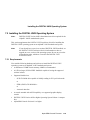
1
About This Manual
This manual describes the AlphaPC 164LX motherboard, a module for computing
systems based on the DIGITAL Semiconductor Alpha 21164 microprocessor and the
companion DIGITAL Semiconductor 21174 core logic chip. It describes the
motherboard’s features and how to set its configuration jumpers. This manual helps
users to install and populate the AlphaPC 164LX motherboard with memory
modules and peripheral cards.
1.1 Manual Conventions and Terminology
The following conventions are used in this manual.
Caution: Cautions indicate potential damage to equipment, software, or data.
Note: Notes provide additional information about a topic.
Numbering: All numbers are decimal or hexadecimal unless otherwise indicated. In
case of ambiguity, a subscript indicates the radix of nondecimal numbers. For
example, 19 is a decimal number, but 1916 and 19A are hexadecimal numbers.
Extents: Extents are specified by a single number or a pair of numbers in square
brackets ([ ]) separated by a colon (:), and are inclusive. For example, bits [7:3]
specify an extent including bits 7, 6, 5, 4, and 3. Multiple bit fields are shown as
extents.
Register Figures: Register figures have bit and field position numbering starting at
the right (low-order) and increasing to the left (high-order).
Signal Names: All signal names are printed in boldface type. Signal names that
originate in an industry-standard specification, such as PCI or IDE, are printed in the
case as found in the specification (usually uppercase). Active low signals have either
a pound sign “#” appended, or a “not” overscore bar; for example, DEVSEL# and
RESET.
About This Manual
1–1
Manual Conventions and Terminology
Italic Type: Italic type emphasizes important information and indicates complete
titles of documents.
Terms: The following terms are used in this manual:
1–2
This term...
Refers to...
Alpha SRM console
DIGITAL UNIX installation guide
DIGITAL UNIX
The Alpha SRM Console firmware
The DIGITAL UNIX Installation Guide
The DIGITAL UNIX operating system
About This Manual
2
Features
Table 2–1 provides an overview of the AlphaPC 164LX motherboard’s features.
Table 2–1 AlphaPC 164LX Features
Feature
Description
Microprocessor
DIGITAL Semiconductor Alpha 21164 microprocessor
(64-bit RISC)
DIGITAL Semiconductor 21174 core logic chip, comprising a single control chip that provides an interface to system memory and
the PCI bus
32MB to 1GB memory array –- Two banks of 128-bit memory;
168-pin unbuffered SDRAM DIMMs
Core logic chip
Synchronous DRAM (SDRAM)
memory
Caching:
L1 Icache
L1 Dcache
L2 Scache
L3 backup cache
I/O and miscellaneous support
Firmware
8KB, direct-mapped instruction cache on the CPU chip
8KB, direct-mapped data cache on the CPU chip
96KB, three-way, set-associative, write-back unified instruction
and data cache on the CPU chip
Onboard 2MB, direct-mapped, synchronous SSRAM backup
cache with 128-bit data path
32-bit and 64-bit, 33-MHz PCI
Two 64-bit and two 32-bit PCI expansion slots
PCI/EIDE control (CMD PCI0646)
Intel 82378ZB PCI-to-ISA bridge chip
Two dedicated ISA expansion slots
SMC FDC37C935 combination controller chip provides control
for diskettes, two UARTs with modem control, parallel port, keyboard, mouse, and time-of-year clock
1MB flash ROM
Alpha SRM Console firmware
Features
2–1
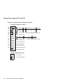
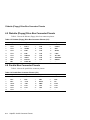
Figure 2–1 shows the AlphaPC 164LX motherboard and its components and
Table 2–2 describes these components.
Figure 2–1 AlphaPC 164LX Jumper/Connector/Component Location
J27
J28
J30
J31
U62
J25
J29
U61
J24
*
*
J26
U58
U59
U60
J23
J18
B1
*
*
*
*
*
*
U50
U49
U48
J17
U53
J16
*
U43
J15
U42
J19
U41
U40
* *
J20
J21
J22
U37
U31
U32
U33
U20
U21
U22
U8
U9
U10
J13
J5
J6
J7
J4
*
*
J3
* Denotes Pin #1
J1
J8
J9
J10
J11
J2
Mouse
J5 Top:
Bottom: Keyboard
J4
Top:
COM1
Bottom: COM2
FM-05933.AI4
2–2
Features
Table 2–2 AlphaPC 164LX Jumper/Connector/Component List
Item No. Description
Item No.
B1
J1
J2
J3
J25
J26
J27
J28
J4
J5
J6
J7
J8
J9
J10
J11
J12
J13
J14
J15
J16
J17
J18
J19
J20
J21
J22
J23
J24
RTC battery (CR2032)
Soft power connector
Fan power, enclosure (+12V)
Power (+3V, +5V, -5V, +12V, -12V)
Description
Hard-drive LED connector
PCI slot 0 (64-bit)
System configuration jumpers
Flash ROM update enable/disable
jumper
COM1/COM2 (DB9) connectors
J29
SROM test port connector
Keyboard/mouse connectors
J30
ISA slot 1
EIDE drive 2/3 connector
J31
ISA slot 0
EIDE drive 0/1 connector
U8 to U10 Cache SRAM (L3)
SDRAM DIMM 0 [0:63] connector
U20 to U22 Cache SRAM (L3)
SDRAM DIMM 1 [64:128] connector U31 to U33 Cache SRAM (L3)
SDRAM DIMM 2 [0:63] connector
U37
I/O interface and address control
(DS 21174-CA)
SDRAM DIMM 3 [64:128] connector U40
Microprocessor, socket
(DS Alpha 21164)
Reserved
U41
Patch 8K PAL
Parallel I/O connector
U42
EIDE controller
Reserved
U43
System clock PLL (CY2308)
Diskette (floppy) drive connector
U48
Microprocessor clock synthesizer
(MC12439)
PCI slot 3 (32-bit)
U49
Serial ROM, socketed (Xilinx
XC17128D)
PCI slot 2 (32-bit)
U50
PCI-to-ISA bridge (Intel 82378ZB)
Microprocessor fan/fan sense connec- U53
Combination controller, Super I/O
tor
(SMC FDC37C935)
Enclosure fan +12V power connector U58
Flash ROM (1MB)
Speaker connector
U59
PCI arbiter PAL
Reset button connector
U60
PCI interrupt request PAL
Halt button connector
U61
Power controller
PCI slot 1 (64-bit)
U62
Power sense
Power LED connector
Features
2–3
Power Requirements
2.1 Power Requirements
The AlphaPC 164LX motherboard has a total power dissipation of 100 W, excluding
any plug-in PCI and ISA devices. Table 2–3 lists the power requirement for each dc
supply voltage.
The power supply must be ATX-compliant.
Table 2–3 Power Supply DC Current Requirements
Voltage/Tolerance
Current1
+3.3 V dc, ±5%
5.0 A
+5 V dc, ±5%
14.0 A
–5 V dc, ±5%
0A
+12 V dc, ±5%
1.0 A
–12 V dc, ±5%
100.0 mA
1
Values indicated are for an AlphaPC 164LX motherboard with an Alpha 21164 microprocessor
operating at 600 MHz, with 64MB SDRAM, excluding adapter cards and disk drives.
Caution:
Fan sensor required. The 21164 microprocessor cooling fan must have
a built-in sensor that will drive a signal if the airflow stops. The sensor is
connected to motherboard connector J18. When the signal is generated,
it resets the system.
2.2 Environmental Requirements
The 21164 microprocessor is cooled by a small fan blowing directly into the chip’s
heat sink. The AlphaPC 164LX motherboard is designed to run efficiently by using
only this fan. Additional fans may be necessary depending upon cabinetry and the
requirements of plug-in cards.
2–4
Features
Physical Parameters
The AlphaPC 164LX motherboard is specified to run within the environment listed
in Table 2–4.
Table 2–4 AlphaPC 164LX Motherboard Environmental Requirements
Parameter
Specification
Operating temperature
10°C to 40°C (50°F to 104°F)
Storage temperature
–55°C to 125°C (–67°F to 257°F)
Relative humidity
10% to 90% with maximum wet bulb temperature 28°C
(82°F) and minimum dew point 2°C (36°F)
Rate of (dry bulb) temperature 11°C/hour ±2°C/hour (20°F/hour ±4°F/hour)
change
2.3 Physical Parameters
The AlphaPC 164LX motherboard is an ATX-size printed-wiring board (PWB) with
the following dimensions:
•
Length: 30.48 cm (12.0 in ±0.0005 in)
•
Width: 24.38 cm (9.6 in ±0.0005 in)
•
Height: 6.86 cm (2.7 in)
Features
2–5
Physical Parameters
2.3.1 ATX Hole Specification
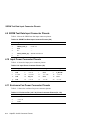
Figure 2–2 shows the ATX Hole Specification for the AlphaPC 164LX.
Figure 2–2 ATX Hole Specification
.800
TYP Between
Connectors
.650
.500
.400
4.900
1.612
1.300
.600
.625
8.950
PCI Connector
(4 Places)
6.100
9.600
ISA Connector
(2 Places)
11.100
12.000
This ATX hole is not supported
on AlphaPC 164LX board, and no
clearance is provided on side 2.
This ATX hole is not supported
on AlphaPC 164LX board,
however clearance is provided
on side 2.
FM-06012.AI4
2–6
Features
Physical Parameters
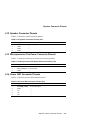
2.3.2 ATX I/O Shield Requirements
Figure 2–3 shows the ATX I/O shield dimensions for the AlphaPC 164LX.
74.8
78.2
85.4
87.2
94.4
98.9
43.5
35.5
24.7
16.7
R 1.00
68.4
64.9
Figure 2–3 ATX I/O Shield Dimensions
21.36
16.05
5.00 TYP
9.25
3.58
2.45
4.35
11.15
15.47
17.95
22.95
23.96
29.10
33.10
90.17
95.40
81.18
70.39
72.19
55.05
64.04
44.26
46.06
37.91
28.92
18.13
19.93
0.99
9.98
11.78
8.00
16.15
14.35
25.14
42.28
40.48
34.13
51.27
64.91
60.26
14.96
R 1.00
7.19 TYP
FM-05986.AI4
Features
2–7
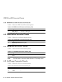
3
AlphaPC 164LX Jumper Configuration
The AlphaPC 164LX motherboard has two groups of jumpers located at J27 and J28,
as shown in Figure 2–1. These jumpers set the hardware configuration and boot
options. Figure 3–1 shows these jumper configurations.
3.1 CPU Speed Selection
The clock synthesizer at location U47 makes it possible to change the frequency of
the microprocessor’s system clock output without having to change the clock crystal.
Simply set the system clock divisor jumpers to adjust the frequency of the
microprocessor’s system clock output. These system clock divisor jumpers are
located at J27–1/2 (IRQ3), J27–3/4 (IRQ2), J27–5/6 (IRQ1), and J27–7/8 (IRQ0).
The jumper configuration is set in IRQ3 through IRQ0. These four jumpers set the
speed at power-up as listed in Figure 3–1. The microprocessor frequency divided by
the ratio determines the system clock frequency.
3.2 Bcache Size Jumpers (CF1 and CF2)
The Bcache size jumpers are located at J27–11/12 (CF) and J27–13/14 (CF2). These
jumpers configure the Bcache as specified in Figure 3–1.
AlphaPC 164LX Jumper Configuration
3–1
Bcache Size Jumpers (CF1 and CF2)
Figure 3–1 AlphaPC 164LX Configuration Jumpers
J27 System Configuration Jumpers
IRQ3
IRQ2
IRQ1
IRQ0
CF0
CF1
CF2
CF3
CF4
CF5
CF6
CF7
1
Frequency Ratio IRQ3 IRQ2 IRQ1 IRQ0
3
5
7
466 MHz
7
In
Out
Out
Out
533 MHz
8
Out
In
In
In
600 MHz
9
Out
In
In
Out
Default
All other combinations are reserved.
9
Reserved (Default Out)
11
13
Bcache Size
CF1
CF2
Comments
2MB
Out
Out
Default
All other combinations are reserved.
15
Reserved (Default Out)
17
Reserved (Default Out)
19
Reserved (Default Out)
21
Reserved (Default Out)
23
Boot_Option (Default Out)
25
Reserved (Default Out)
J28 Flash ROM Update Jumpers
1
1 to 2 In = Disable
2
3
3–2
Comments
2 to 3 In = Enable (Default)
AlphaPC 164LX Jumper Configuration
Boot Option Jumper (CF7)
3.3 Boot Option Jumper (CF7)
The boot option jumper is located at J27–23/24 (CF7). The default position for this
jumper is out (Figure 3–1). This jumper selects the image to be loaded into memory
from the system flash ROM. With the jumper out, the SRM Console firmware is
loaded. With the jumper in, the fail-safe booter is loaded. For more information
about the fail-safe booter, refer to Section 8.4.
3.4 Flash ROM Update Jumper (J28)
When J28–2/3 are jumpered together (default), the flash ROM is write-enabled.
When J28–1/2 are jumpered together, the flash ROM is write-protected.
AlphaPC 164LX Jumper Configuration
3–3
4
AlphaPC 164LX Connector Pinouts
This chapter contains pinouts for all of the AlphaPC 164LX connectors. See
Figure 2–1 for connector locations.
4.1 PCI Bus Connector Pinouts
Table 4–1 shows the PCI bus connector pinouts.
Table 4–1 PCI Bus Connector Pinouts
Pin
Signal
Pin
Signal
(Sheet 1 of 2)
Pin
Signal
Pin
Signal
TMS
INTC
—
RST#
—
AD[26]
+3V
AD[18]
Gnd
+3V
PAR
AD[11]
Not used
AD[04]
Vdd
-12V
Vdd
PRSNT1#
A4
A8
A12
A16
A20
A24
A28
A32
A36
A40
A44
A48
A52
A56
A60
B2
B6
B10
TDI
Vdd
Gnd
Vdd
AD[30]
Gnd
AD[22]
AD[16]
TRDY#
SDONE
AD[15]
Gnd
C/BE#[0]
Gnd
REQ64#
TCK
Vdd
—
32-Bit and 64-Bit PCI Connectors (J16, J17, J23, J26)
A1
A5
A9
A13
A17
A21
A25
A29
A33
A37
A41
A45
A49
A53
A57
A61
B3
B7
TRST#
Vdd
—
Gnd
GNT#
+3V
AD[24]
AD[20]
+3V
STOP#
SBO#
+3V
AD[09]
+3V
AD[02]
Vdd
Gnd
INTB
A2
A6
A10
A14
A18
A22
A26
A30
A34
A38
A42
A46
A50
A54
A58
A62
B4
B8
+12V
INTA
Vdd
—
Gnd
AD[28]
IDSEL
Gnd
FRAME#
STOP#
Gnd
AD[13]
Not used
AD[06]
AD[00]
Vdd
TDO
INTD
A3
A7
A11
A15
A19
A23
A27
A31
A35
A39
A43
A47
A51
A55
A59
B1
B5
B9
AlphaPC 164LX Connector Pinouts
4–1
PCI Bus Connector Pinouts
Table 4–1 PCI Bus Connector Pinouts
(Sheet 2 of 2)
Pin
Signal
Pin
Signal
Pin
Signal
Pin
Signal
B11
B15
B19
B23
B27
B31
B35
B39
B43
B47
B51
B55
B59
PRSNT2#
Gnd
Vdd
AD[27]
AD[23]
+3V
IRDY#
LOCK#
+3V
AD[12]
Not used
AD[05]
Vdd
B12
B16
B20
B24
B28
B32
B36
B40
B44
B48
B52
B56
B60
Gnd
CLK
AD[31]
AD[25]
Gnd
AD[17]
+3V
PERR#
C/BE#[1]
AD[10]
AD[08]
AD[03]
ACK64#
B13
B17
B21
B25
B29
B33
B37
B41
B45
B49
B53
B57
B61
Gnd
Gnd
AD[29]
+3V
AD[21]
C/BE#[2]
DEVSEL#
+3V
AD[14]
Gnd
AD[07]
Gnd
Vdd
B14
B18
B22
B26
B30
B34
B38
B42
B46
B50
B54
B58
B62
—
REQ#
Gnd
C/BE#[3]
AD[19]
Gnd
Gnd
SERR#
Gnd
Not used
+3V
AD[01]
Vdd
A65
A69
A73
A77
A81
A85
A89
A93
B65
B69
B73
B77
B81
B85
B89
B93
C/BE#[5]
Gnd
D[56]
D[50]
Gnd
D[40]
D[34]
Gnd
C/BE#[6]
D[61]
Gnd
D[51]
D[45]
Gnd
D[35]
—
A66
A70
A74
A78
A82
A86
A90
A94
B66
B70
B74
B78
B82
B86
B90
B94
Vdd
D[60]
D[54]
Gnd
D[44]
D[38]
Gnd
—
C/BE#[4]
Vdd
D[55]
D[49]
Gnd
D[39]
D[33]
Gnd
64-Bit PCI Connectors Only (J23, J26)
A63
A67
A71
A75
A79
A83
A87
A91
B63
B67
B71
B75
B79
B83
B87
B91
4–2
Gnd
PAR64
D[58]
Vdd
D[48]
D[42]
Gnd
D[32]
—
Gnd
D[59]
D[53]
Vdd
D[43]
D[37]
Gnd
A64
A68
A72
A76
A80
A84
A88
A92
B64
B68
B72
B76
B80
B84
B88
B92
C/BE#[7]
D[62]
Gnd
D[52]
D[46]
Vdd
D[36]
—
Gnd
D[63]
D[57]
Gnd
D[47]
D[41]
Vdd
—
AlphaPC 164LX Connector Pinouts
ISA Expansion Bus Connector Pinouts
4.2 ISA Expansion Bus Connector Pinouts
Table 4–2 shows the ISA expansion bus connector pinouts.
Table 4–2 ISA Expansion Bus Connector Pinouts (J30, J31)
Pin
Signal
Pin
Signal
Pin
Signal
Pin
Signal
1
5
9
13
17
21
25
29
33
37
41
45
49
53
57
61
65
69
73
77
81
85
89
93
97
Gnd
Vdd
–5V
–12V
+12V
SMEMW#
IOW#
DACK3#
DACK1#
REFRESH#
IRQ7
IRQ5
IRQ3
TC
Vdd
Gnd
IOCS16#
IRQ11
IRQ15
DACK0#
DACK5#
DACK6#
DACK7#
Vdd
Gnd
2
6
10
14
18
22
26
30
34
38
42
46
50
54
58
62
66
70
74
78
82
86
90
94
98
IOCHCK#
SD6
SD4
SD2
SD0
AEN
SA18
SA16
SA14
SA12
SA10
SA8
SA6
SA4
SA2
SA0
LA23
LA21
LA19
LA17
MEMW#
SD9
SD11
SD13
SD15
3
7
11
15
19
23
27
31
35
39
43
47
51
55
59
63
67
71
75
79
83
87
91
95
—
RSTDRV
IRQ9
DRQ2
ZEROWS#
Gnd
SMEMR#
IOR#
DRQ3
DRQ1
SYSCLK
IRQ6
IRQ4
DACK2#
BALE
OSC
MEMCS16#
IRQ10
IRQ12
IRQ14
DRQ0
DRQ5
DRQ6
DRQ7
MASTER#
—
4
8
12
16
20
24
28
32
36
40
44
48
52
56
60
64
68
72
76
80
84
88
92
96
—
SD7
SD5
SD3
SD1
IOCHRDY
SA19
SA17
SA15
SA13
SA11
SA9
SA7
SA5
SA3
SA1
SBHE#
LA22
LA20
LA18
MEMR#
SD8
SD10
SD12
SD14
—
AlphaPC 164LX Connector Pinouts
4–3
SDRAM DIMM Connector Pinouts
4.3 SDRAM DIMM Connector Pinouts
Table 4–3 shows the SDRAM DIMM connector pinouts.
Table 4–3 SDRAM DIMM Connector Pinouts (J8 through J11)1
(Sheet 1 of 2)
Pin
Signal
Pin
Signal
Pin
Signal
Pin
Signal
1
5
9
13
17
21
25
29
33
37
41
45
49
53
57
61
65
69
73
77
81
85
89
93
97
101
105
109
113
117
121
Gnd
DQ3
DQ6
DQ9
DQ13
CB0
NC
DQMB1
A0
A8
+3V
S2
+3V
CB3
DQ18
NC
DQ21
DQ24
+3V
DQ31
NC
Gnd
DQ35
DQ38
DQ41
DQ45
CB4
NC
DQMB5
A1
A9
2
6
10
14
18
22
26
30
34
38
42
46
50
54
58
62
66
70
74
78
82
86
90
94
98
102
106
110
114
118
122
DQ0
+3V
DQ7
DQ10
+3V
CB1
+3V
S0
A2
A10
CK0
DQMB2
NC
Gnd
DQ19
NC
DQ22
DQ25
DQ28
Gnd
SDA
DQ32
+3V
DQ39
DQ42
+3V
CB5
+3V
S1
A3
BA0
3
7
11
15
19
23
27
31
35
39
43
47
51
55
59
63
67
71
75
79
83
87
91
95
99
103
107
111
115
119
123
DQ1
DQ4
DQ8
DQ11
DQ14
Gnd
WE
NC
A4
A12
Gnd
DQMB3
NC
DQ16
+3V
CKE1
DQ23
DQ26
DQ29
CK2
SCL
DQ33
DQ36
DQ40
DQ43
DQ46
Gnd
CAS
RAS
A5
A13
4
8
12
16
20
24
28
32
36
40
44
48
52
56
60
64
68
72
76
80
84
88
92
96
100
104
108
112
116
120
124
DQ2
DQ5
Gnd
DQ12
DQ15
NC
DQMB0
Gnd
A6
+3V
NC
NC
CB2
DQ17
DQ20
Gnd
Gnd
DQ27
DQ30
NC
+3V
DQ34
DQ37
Gnd
DQ44
DQ47
NC
DQMB4
Gnd
A7
+3V
4–4
AlphaPC 164LX Connector Pinouts
EIDE Drive Bus Connector Pinouts
Table 4–3 SDRAM DIMM Connector Pinouts (J8 through J11)1
Pin
125
129
133
137
141
145
149
153
157
161
165
Signal
CK1
S3
+3V
CB7
DQ50
NC
DQ53
DQ56
+3V
DQ63
SA0
Pin
126
130
134
138
142
146
150
154
158
162
166
Signal
2
BA1
DQMB6
NC
Gnd
DQ51
NC
DQ54
DQ57
DQ60
Gnd
SA1
(Sheet 2 of 2)
Pin
Signal
Pin
Signal
127
131
135
139
143
147
151
155
159
163
167
Gnd
DQMB7
NC
DQ48
+3V
PD
DQ55
DQ58
DQ61
CK3
SA2
128
132
136
140
144
148
152
156
160
164
168
CKE0
PD3
CB6
DQ49
DQ52
Gnd
Gnd
DQ59
DQ62
NC
+3V
1
2
Pins 1 through 84 are on the front side and pins 85 through 168 are on the back side.
The AlphaPC 164LX uses BA1 as both BA1 and ADDR12. Therefore, four-bank DIMMs using ADDR[11:0]
are the maximum size. (Two-bank DIMMs can use ADDR[12:0].)
3 Pull-down.
4.4 EIDE Drive Bus Connector Pinouts
Table 4–4 shows the EIDE drive bus connector pinouts.
Table 4–4 EIDE Drive Bus Connector Pinouts (J6, J7)
Pin
Signal
Pin
Signal
Pin
Signal
Pin
Signal
1
5
9
13
17
21
25
29
33
37
RESET
IDE_D6
IDE_D4
IDE_D2
IDE_D0
MARQ
IOR
MACK
ADDR1
CS0
2
6
10
14
18
22
26
30
34
38
Gnd
IDE_D9
IDE_D11
IDE_D13
IDE_D15
Gnd
Gnd
Gnd
NC
CS1
3
7
11
15
19
23
27
31
35
39
IDE_D7
IDE_D5
IDE_D3
IDE_D1
Gnd
IOW
CHRDY
IRQ
ADDR0
ACT
4
8
12
16
20
24
28
32
36
40
IDE_D8
IDE_D10
IDE_D12
IDE_D14
NC (key pin)
Gnd
BALE
IOCS16
ADDR2
Gnd
AlphaPC 164LX Connector Pinouts
4–5
Diskette (Floppy) Drive Bus Connector Pinouts
4.5 Diskette (Floppy) Drive Bus Connector Pinouts
Table 4–5 shows the diskette (floppy) drive bus connector pinouts.
Table 4–5 Diskette (Floppy) Drive Bus Connector Pinouts (J15)
Pin
Signal
Pin
Signal
Pin
Signal
Pin
Signal
1
5
9
13
17
21
25
29
33
Gnd
Gnd
Gnd
Gnd
Gnd
Gnd
Gnd
ID0
ID1
2
6
10
14
18
22
26
30
34
DEN0
DEN1
MTR0
DR0
DIR
WDATA
TRK0
RDATA
DSKCHG
3
7
11
15
19
23
27
31
—
Gnd
Gnd
Gnd
Gnd
Gnd
Gnd
Gnd
Gnd
—
4
8
12
16
20
24
28
32
—
NC
INDEX
DR1
MTR1
STEP
WGATE
WRTPRT
HDSEL
—
4.6 Parallel Bus Connector Pinouts
Table 4–6 shows the parallel bus connector pinouts.
Table 4–6 Parallel Bus Connector Pinouts (J13)
Pin
Signal
Pin
Signal
Pin
Signal
Pin
Signal
1
5
9
13
17
21
25
STB
PD3
PD7
SLCT
SLIN
Gnd
Gnd
2
6
10
14
18
22
—
PD0
PD4
ACK
AFD
Gnd
Gnd
—
3
7
11
15
19
23
—
PD1
PD5
BUSY
ERR
Gnd
Gnd
—
4
8
12
16
20
24
—
PD2
PD6
PE
INIT
Gnd
Gnd
—
4–6
AlphaPC 164LX Connector Pinouts
COM1/COM2 Serial Line Connector Pinouts
4.7 COM1/COM2 Serial Line Connector Pinouts
Table 4–7 shows the COM1/COM2 serial line connector pinouts.
Table 4–7 COM1/COM2 Serial Line Connector Pinouts (J4)
COM1 Pin
(Top)
COM1 Signal
COM2 Pin
(Bottom)
COM2 Signal
1
2
3
4
5
6
7
8
9
DCD1
RxD1
TxD1
DTR1
SG1
DSR1
RTS1
CTS1
RI1
1
2
3
4
5
6
7
8
9
DCD2
RxD2
TxD2
DTR2
SG2
DSR2
RTS2
CTS2
RI2
4.8 Keyboard/Mouse Connector Pinouts
Table 4–8 shows the keyboard/mouse connector pinouts.
Table 4–8 Keyboard/Mouse Connector Pinouts (J5)
Keyboard Pin
(Top)
Keyboard Signal
Mouse Pin
(Bottom)
Mouse Signal
1
2
3
4
5
6
1
2
3
4
5
6
MSDATA
NC
Gnd
Vdd
MSCLK
NC
KBDATA
NC
Gnd
Vdd
KBCLK
NC
AlphaPC 164LX Connector Pinouts
4–7
SROM Test Data Input Connector Pinouts
4.9 SROM Test Data Input Connector Pinouts
Table 4–9 shows the SROM test data input connector pinouts.
Table 4–9 SROM Test Data Input Connector Pinouts (J29)
Pin
Signal
Name
1
2
3
4
5
6
NC
SROM_CLK_L
Gnd
NC
TEST_SROM_D_L
NC
—
Clock out
—
—
SROM serial data in
—
4.10 Input Power Connector Pinouts
Table 4–10 shows the input power connector pinouts.
Table 4–10 Input Power Connector Pinouts (J3)1
Pin
Voltage
Pin
Voltage
Pin
Voltage
Pin
Voltage
1
5
9
13
17
+3.3 V dc
Gnd
5 V SB
Gnd
Gnd
2
6
10
14
18
+3.3 V dc
+5 V dc
+12 V dc
PS_ON
–5 V dc
3
7
11
15
19
Gnd
Gnd
+3.3 V dc
Gnd
+5 V dc
4
8
12
16
20
+5 V dc
P_DCOK
–12 V dc
Gnd
+5 V dc
1
This pinout is ATX-compliant.
4.11 Enclosure Fan Power Connector Pinouts
Table 4–11 shows the enclosure fan power connector pinouts.
Table 4–11 Enclosure Fan (+12 V dc) Power Connector Pinouts (J2, J19)
4–8
Pin
Voltage
1
2
3
Gnd
+12 V dc
Gnd
AlphaPC 164LX Connector Pinouts
Speaker Connector Pinouts
4.12 Speaker Connector Pinouts
Table 4–12 shows the speaker connector pinouts.
Table 4–12 Speaker Connector Pinouts (J20)
Pin
Signal
Name
1
2
3
4
SPKR
Gnd
Gnd
Gnd
Speaker output
—
—
—
4.13 Microprocessor Fan Power Connector Pinouts
Table 4–13 shows the microprocessor fan power connector pinouts.
Table 4–13 Microprocessor Fan Power Connector Pinouts (J18)
Pin
Signal
Name
1
2
3
+12 V dc
—
FAN_CONN_L Fan connected
Gnd
—
4.14 Power LED Connector Pinouts
Table 4–14 shows the power LED connector pinouts.
Table 4–14 Power LED Connector Pinouts (J24)
Pin
Signal
Name
1
2
3
4
5
POWER_LED_L
Gnd
NC
NC
NC
Power LED input
—
—
—
—
AlphaPC 164LX Connector Pinouts
4–9
EIDE Drive LED Connector Pinouts
4.15 EIDE Drive LED Connector Pinouts
Table 4–15 shows the EIDE drive LED connector pinouts.
Table 4–15 EIDE Drive LED Connector Pinouts (J25)
Pin
Signal
Name
1
2
HD_ACT_L
HD_LED_L
Hard drive active
Hard drive LED input
4.16 Reset Button Connector Pinouts
Table 4–16 shows the reset button connector pinouts.
Table 4–16 Reset Button Connector Pinouts (J21)
Pin
Signal
Name
1
2
RESET_BUTTON Reset system
Gnd
—
4.17 Halt Button Connector Pinouts
Table 4–17 shows the halt button connector pinouts.
Table 4–17 Halt Button Connector Pinouts (J22)
Pin
Signal
1
2
HALT_BUTTON Halt system
Gnd
—
Note:
Name
The Halt button is not used with the Windows NT operating system.
4.18 Soft Power Connector Pinouts
Table 4–18 shows the soft power connector pinouts.
Table 4–18 Soft Power Connector Pinouts (J1)
4–10
Pin
Signal
Name
1
2
Input
Gnd
System power on/off
—
AlphaPC 164LX Connector Pinouts
5
Memory and Microprocessor Configuration
For higher system speed or greater throughput, you can upgrade SDRAM memory
by replacing DIMMs with those of greater size.
When configuring or upgrading SDRAM, observe the following rules:
•
Each DIMM must be a 168-pin unbuffered version and have a frequency of
100 MHz.
•
All DIMMs must be of equal size if they are in the same bank.
5.1 Configuring SDRAM Memory
Although not an exhaustive list, Table 5–1 lists the tested SDRAM memory
configurations available.
For a list of vendors who supply components and accessories for the AlphaPC
164LX, see Appendix A.
Refer to Figure 2–1 for DIMM connector locations.
Note:
1Mb × 72 is not supported.
Table 5–1 AlphaPC 164LX SDRAM Memory Configurations
(Sheet 1 of 2)
Total
Memory
Bank 0 (J8 and J9)
Bank 1 (J10 and J11)
32MB
64MB
2Mb × 72
2Mb × 72
—
2Mb X 72
96MB
4Mb X 72
4Mb X 72
—
2Mb X 72
Memory and Microprocessor Configuration
5–1
Upgrading SDRAM Memory
Table 5–1 AlphaPC 164LX SDRAM Memory Configurations
(Sheet 2 of 2)
Total
Memory
Bank 0 (J8 and J9)
Bank 1 (J10 and J11)
128MB
4Mb × 72
4Mb × 72
160MB
192MB
256MB
8Mb × 72
8Mb × 72
8Mb × 72
8Mb × 72
—
2Mb × 72
4Mb × 72
8Mb × 72
512MB
16Mb × 72
16Mb × 72
—
16Mb × 72
768MB
1GB
32Mb × 72
32Mb × 72
32Mb × 72
—
16Mb × 72
32Mb × 72
5.2 Upgrading SDRAM Memory
You can upgrade memory in the AlphaPC 164LX by adding more DIMMs or
replacing the ones that you have with a greater size. Refer to Figure 2–1 for DIMM
connector locations.
Use the following general guidelines:
1. Observe antistatic precautions. Handle DIMMs only at the edges to prevent
damage.
2. Remove power from the system.
3. Open levers and align the DIMM.
4. Firmly push the module into the connector. Ensure that the DIMM snaps into the
plastic locking levers on both ends.
5. Restore power to the system.
5–2
Memory and Microprocessor Configuration
Increasing Microprocessor Speed
5.3 Increasing Microprocessor Speed
This section describes how to complete the following actions to increase
microprocessor speed:
•
Replace the DIGITAL Semiconductor 21164 microprocessor with an Alpha chip
that has a higher speed rating.
•
Reconfigure the clock divisor jumpers.
5.3.1 Preparatory Information
Caution:
Static-Sensitive Component – Due to the sensitive nature of electronic
components to static electricity, anyone handling the microprocessor
must wear a properly grounded antistatic wriststrap. Use of antistatic
mats, ESD approved workstations, or exercising other good ESD practices is recommended.
A DIGITAL Semiconductor 21164 microprocessor with a higher speed rating is
available from your local distributor. See Appendix A for information about
supporting products.
When replacing the microprocessor chip, also replace the thermal conducting
GRAFOIL pad. See Appendix A for information about the parts kit, which includes
the heat sink, GRAFOIL pad, two hex nuts, heat-sink clips, 60-mm fan, fan guard,
and four screws.
5.3.2 Required Tools
The following tools are required when replacing the microprocessor chip:
A TS30 manual nut/torque driver (or equivalent) with the following attachments is
required to affix the heat sink and fan to the microprocessor’s IPGA package:
•
1/4-inch hex bit
•
7/16-inch socket with 1/4-inch hex drive
•
#2 Phillips-head screwdriver bit
Memory and Microprocessor Configuration
5–3
Increasing Microprocessor Speed
5.3.3 Removing the 21164 Microprocessor
Remove the microprocessor currently in place at location U40 by performing the
following steps:
1. Unplug the fan power/sensor cable from connector J18 (see Figure 2–1).
2. Remove the four 6-32 X 0.875-inch screws that secure the fan and fan guard to
the heat sink.
3. Remove the fan and fan guard.
4. If the sink/chip/fan clip is used, remove it by unhooking its ends from around the
ZIF socket retainers.
5. Using a 7/16-inch socket, remove the two nuts securing the heat sink to the
microprocessor studs.
6. Remove the heat sink by gently lifting it off the microprocessor.
7. Remove and discard the GRAFOIL heat conduction pad.
8. Thoroughly clean the bottom surface of the heat sink before affixing it to the
new microprocessor.
9. Lift the ZIF socket actuator handle to a full 90° angle.
10. Remove the microprocessor chip by lifting it straight out of the socket.
5.3.4 Installing the 21164 Microprocessor
Install the new microprocessor in location U40 by performing the following steps:
Note:
Install the heat sink only after the microprocessor has been assembled to
the ZIF socket.
1. Observe antistatic precautions.
2. Lift the ZIF socket actuator handle to a full 90° angle.
3. Ensure that all the pins on the microprocessor package are straight.
4. The ZIF socket and microprocessor are keyed to allow for proper installation.
Align the microprocessor, with its missing AD01 pin, with the corresponding
plugged AD01 position on the ZIF socket. Gently lower into position.
5. Close the ZIF socket actuator handle to its locked position.
5–4
Memory and Microprocessor Configuration
Increasing Microprocessor Speed
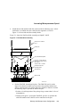
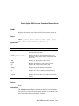
6. Install the heat sink and heat-sink fan as directed in the following steps. A heatsink/fan kit is available from the vendor listed in Appendix A. Refer to
Figure 5–1 for heat-sink and fan assembly details.
Figure 5–1 shows the Fan/Heat-Sink Assembly on AlphaPC 164LX.
Figure 5–1 Fan/Heat-Sink Assembly
Screw, 6-32 x 0.875 in
Qty 4
Guard, Fan
Fan
Clip, Heat Sink/Chip/Fan
Nut, Hex, 1/4-20, 2011-T3
Aluminum, 0.438 in Across
Flats, Qty 2
Torque to 20 +/- 2 in-lbs
Heat Sink, with Fan
Mounting Holes
Thermal Pad
Airflow
Alpha 21164
FM-06013.AI4
a. Put the GRAFOIL thermal pad in place. The GRAFOIL pad is used to
improve the thermal conductivity between the chip package and the heat
sink by replacing micro air pockets with a less insulative material. Perform
the following steps to position the GRAFOIL pad:
1. Perform a visual inspection of the package slug to ensure that it is free of
contamination.
2. Wearing clean gloves, pick up the GRAFOIL pad. Do not perform this
with bare hands because skin oils can be transferred to the pad.
Memory and Microprocessor Configuration
5–5
Increasing Microprocessor Speed
3. Place the GRAFOIL pad on the gold-plated slug surface and align it with
the threaded studs.
b. Attach the microprocessor heat sink. The heat-sink material is clear anodized, hot-water-sealed, 6061-T6 aluminum. The nut material is 2011-T3 aluminum (this grade is critical). Perform the following steps to attach the heat
sink:
1. Observe antistatic precautions.
2. Align the heat-sink holes with the threaded studs on the ceramic package.
3. Handle the heat sink by the edges and lower it onto the chip package,
taking care not to damage the stud threads.
4. Set a calibrated torque driver to 20 in-lbs, ±2 in-lbs (2.3 Nm, ±0.2 Nm).
The torque driver should have a mounted 7/16-inch socket.
5. Insert a nut into the 7/16-inch socket, place on one of the studs, and
tighten to the specified torque. Repeat for the second nut.
6. If the sink/chip/fan clip is used, properly install it by positioning it over
the assembly and hooking its ends around the ZIF socket retainers.
c. Attach the heat-sink fan assembly:
1. Place the fan assembly on top of the heat sink, aligning the fan mounting
holes with the corresponding threaded heat-sink holes. Align the fan so
that the fan power/sensor wires exit the fan closest to connector J18 (see
Figure 2–1). Fan airflow must be directed into the heat sink (fan label
facing down toward the heat sink).
2. Place the fan guard on top of the fan. Orient the guard so that the corner
mounting areas lay flush against the heat sink.
3. Secure the fan and fan guard to the heat sink with four 6-32 X 0.875-inch
screws.
4. Plug the fan power/sensor cable into connector J18.
Important: When installing the microprocessor, you must change the frequency of
its clock output by setting the system clock divisor jumpers, as described
in Section 3.1.
5–6
Memory and Microprocessor Configuration
6
Interrupts and ISA Bus Addresses
This section lists the system and I/O interrupt assignments. It also lists the physical
AlphaPC 164LX I/O space assignments.
6.1 Interrupts
Table 6–1 lists each AlphaPC 164LX ISA interrupt and its source.
Table 6–1 ISA Interrupts
(Sheet 1 of 2)
Interrupt Number Interrupt Source
IRQ0
Internal timer 1
IRQ1
Keyboard
IRQ2
Interrupt from controller 2
IRQ3
COM2
IRQ4
COM1
IRQ5
Available
IRQ6
Diskette (floppy)
IRQ7
Parallel port
IRQ8#1
Reserved
IRQ9
Available
IRQ10
Available
IRQ11
Available
IRQ12
Mouse
Interrupts and ISA Bus Addresses
6–1
ISA I/O Address Map
Table 6–1 ISA Interrupts
Interrupt Number Interrupt Source
IRQ13
Available
IRQ14
EIDE
IRQ15
EIDE
1
The # symbol indicates an active low signal.
6.2 ISA I/O Address Map
Table 6–2 lists the AlphaPC 164LX ISA I/O space address mapping.
Table 6–2 ISA I/O Address Map
6–2
Range (hex)
Usage
000-00F
8237 DMA #1
020-021
8259 PIC #1
040-043
8253 timer
060-061
Ubus IRQ12 and NMI control
070
CMOS RAM address and NMI mask register
080-08F
DMA page registers
0A0-0A1
8259 PIC #2
0C0-0DF
8237 DMA #2
2F8-2FF
Serial port—COM2
370-377
Secondary diskette (floppy)
3BC-3BF
Parallel port—LPT1
3F0-3F7
Primary diskette (floppy)
3F8-3FF
Serial port—COM1
800
FLASH_ADR19 register
801
AlphaPC 164LX configuration register
804-806
PCI interrupt registers
Interrupts and ISA Bus Addresses
(Sheet 2 of 2)
ISA I/O Address Map
6.2.1 Flash ROM Address Map
The address range for the flash ROM is FFF8.0000–FFFF.FFFF. Flash space of 1MB
is obtained by double mapping this 512KB space. FLASH_ADR19 register at I/O
location 80016 provides this function. Writing a 0 to this location enables the lower
512KB of flash. Writing a 1 to this location enables the upper 512KB of flash.
Interrupts and ISA Bus Addresses
6–3
7
Alpha SRM Console Firmware
The Alpha SRM Console firmware initializes the system and enables you to install
and boot the DIGITAL UNIX operating system. This firmware resides in the flash
ROM on the AlphaPC 164LX motherboard.
7.1 Alpha SRM Console Firmware Conventions
The following conventions are used in this section:
Convention
Description
>>>
Alpha SRM Console prompt.
Backslash (\) at the end of a line
Continuation symbol to continue long commands
on the next line.
_>
Continuation line prompt.
Maximum command length
255 characters.
Multiple contiguous spaces or tabs Treated as a single space.
Command abbreviations
Allowed, if not ambiguous.
Command qualifiers or options
Prefix with a space and a dash (-).
Numbers
Hexadecimal, unless otherwise specified.
(Registers, such as R0–R31, are shown in
decimal notation.)
Alpha SRM Console Firmware
7–1
Alpha SRM Console Firmware Conventions
The following table lists Alpha SRM Console special keys and their functions. These
special keys, also referred to as shortcut keys, provide command recall, line editing,
and basic input/output control flow.
7–2
Shortcut Key
Function
Enter
Terminate the command line input.
Backspace or
Delete
Delete one character to the left of the cursor.
Ctrl/A
Toggles insert/overstrike mode. (Overstrike is the default.)
Ctrl/B
Up arrow
Down arrow
Recall previous commands. (The last 16 commands are
stored.)
Ctrl/C
Terminate the foreground process.
Ctrl/D
Left arrow
Move the cursor one position to the left.
Ctrl/E
Move the cursor to the end of the line.
Ctrl/F
Right arrow
Move the cursor one position to the right.
Ctrl/H
Move the cursor to the beginning of the line.
Ctrl/O
Suppress or resume (toggle) console output.
Ctrl/Q
Resume the flow (XON) of data to the console.
Ctrl/R
Retype the current command line.
Ctrl/S
Stop the flow (XOFF) of data to the console.
Ctrl/U
Delete the entire line.
Alpha SRM Console Firmware
Basic Alpha SRM Console Command Descriptions
7.2 Basic Alpha SRM Console Command Descriptions
This section describes the following basic Alpha SRM Console commands that are
necessary to boot the DIGITAL UNIX operating system:
•
arc
•
boot
•
deposit
•
examine
•
fwupdate
•
set
•
show
The Alpha SRM Console offers additional commands. For a complete list of Alpha
SRM Console commands, enter help at the Alpha SRM Console prompt (>>>).
Alpha SRM Console Firmware
7–3
Basic Alpha SRM Console Command Descriptions
arc
Loads and runs the AlphaBIOS firmware update utility from a
diskette.
Syntax
arc
nt
Arguments
None
Options
None
Description
None
Examples
Either of the following commands load and run the AlphaBIOS
firmware update utility from a diskette:
>>>arc
or
>>>nt
7–4
Alpha SRM Console Firmware
Basic Alpha SRM Console Command Descriptions
boot
Initializes the processor, loads a program image from the specified
boot device, and transfers control to the loaded image.
Syntax
boot [-file <filename>] [-flags
<longword>[,<longword>]]
[-protocols <enet_protocol>] [-halt]
[<boot_device>]
Arguments
<boot_device>
A device path or list of devices from which the firmware will attempt
to boot. Use the set bootdef_dev command to set an
environment variable that specifies a default boot device.
Options
boot Command Option
Description
-file <filename>
Specifies the name of a file to load into the system. Use
the set boot_file command to set the
environment variable that specifies a default boot file.
-flags
<longword> [,<longword>]
Specifies additional information for the operating
system. For DIGITAL UNIX systems, the following
values may be used:
i = Interactive boot
s = Boot to single user
a = Autoboot to multiuser
Use the set boot_osflags command to set an
environment variable that specifies a default boot flag
value.
-protocols
<enet_protocol>
Specifies the Ethernet protocols that will be used for a
network boot. Values may be mop or bootp.
-halt
Forces the bootstrap operation to halt and invoke the
console program after the image is loaded and the page
tables and other data structures are set up.
Alpha SRM Console Firmware
7–5
Basic Alpha SRM Console Command Descriptions
Description
The boot command initializes the processor, loads a program image
from the specified boot device, and transfers control to that image. If
you do not specify a boot device in the command line, the default
boot device is used. The default boot device is determined by the
value of the bootdef_dev environment variable.
If you specify a list of devices, a bootstrap is attempted from each
device in the order in which the device is listed. Then control passes
to the first successfully booted image. In a list, always enter network
devices last because network bootstraps terminate only if a fatal error
occurs or if an image is successfully loaded.
The -flags option can pass additional information to the operating
system about the boot that you are requesting. On an OpenVMS
system, the -flags option specifies the system root number and
boot flags. If you do not specify a boot flag qualifier, the default boot
flag’s value specified by the boot_osflags environment variable is
used.
The -protocols option allows selection of either the DECnet
MOP or the TCP/IP BOOTP network protocols. The keywords mop
and bootp are valid arguments for this option. It is possible to set the
default protocol for a port by setting the environment variable
ewa0_protocols or era0_protocols to the appropriate protocol.
Explicitly stating the boot flags or the boot device overrides the
current default value for the current boot request, but does not change
the corresponding environment variable.
See the Environment Variables for Alpha SRM Console Commands
section in this chapter for more information about environment
variables.
7–6
Alpha SRM Console Firmware
Basic Alpha SRM Console Command Descriptions
Examples
boot Command Example
Description
>>>boot
Boots the system from the default boot device.
>>>boot ewa0
Boots the system from Ethernet port ewa0.
>>>boot -file dec2.sys ewa0
Boots the file named dec2.sys from Ethernet
port ewa0.
>>>boot -protocol bootp ewa0
Boots the system using the TCP/IP BOOTP
protocol from Ethernet port ewa0.
>>>boot -flags 0,1
Boots the system from the default boot device
using flag setting 0,1.
>>>boot -halt dka0
Loads the bootstrap image from disk dka0,
halts the bootstrap operation, and invokes the
console program. Subsequently, you can enter
continue to transfer control to the operating
system.
Alpha SRM Console Firmware
7–7
Basic Alpha SRM Console Command Descriptions
deposit
Writes data to the specified address.
Syntax
deposit [-{b,w,l,q,o,h}] [{physical, virtual, gpr,
fpr, ipr}] [-n <count>] [-s <step>]
[<device>:]<address> <data>
Arguments
<device>:
The optional device name (or address space) selects the device to
access. The following platform-independent devices are supported:
•
pmem
Physical memory.
•
vmem
Virtual memory. All access and protection checking occur.
If the access is not allowed to a program running with the
current processor status (PS), the console issues an error
message. If memory mapping is not enabled, virtual
addresses are equal to physical addresses.
<address>
An address that specifies the offset within a device into which data is
deposited. The address may be any legal symbolic address.
Valid symbolic addresses are shown in the following table.
7–8
Symbolic
Address
Description
gpr-name
Represents general-purpose register.
ipr-name
Represents internal processor register.
PC
Program counter.
+
The location immediately following the last location referenced by
examine or deposit.
Alpha SRM Console Firmware
Basic Alpha SRM Console Command Descriptions
Symbolic
Address
Description
-
The location immediately preceding the last location referenced by
examine or deposit.
*
The location last referenced by examine or deposit.
@
The location addressed by the last location referenced by examine or
deposit.
<data>
The data to be deposited.
Options
deposit Command Option
Description
-b
Specifies data type is byte.
-w
Specifies data type is word.
-l
Specifies data type is longword.
-q
Specifies data type is quadword.
-o
Specifies data type is octaword.
-h
Specifies data type is hexword.
-physical
References physical address space.
-virtual
References virtual address space.
-gpr
References general-purpose register address space.
-fpr
References floating-point register address space.
-ipr
References internal processor register address space.
-n <count>
Specifies the number of consecutive locations to
examine.
-s <step>
Specifies the address increment as a hexadecimal value.
This option allows you to override the increment that is
normally derived from the data size.
Alpha SRM Console Firmware
7–9
Basic Alpha SRM Console Command Descriptions
Description
The deposit command writes data to the specified address, such as
a memory location, register, device, or file. The defaults for address
space, data size, and address are the last specified values. After
initialization, the default for address space is physical memory; for
data size, the default is a quadword; and for address, the default is
zero.
An address or device can be specified by concatenating the device
name with the address. For example, use pmem:0 and specify the
size of the address space to be written. If a conflicting device,
address, or data size is specified, the console ignores the command
and issues an error response.
Examples
7–10
deposit Command Example
Description
>>>d -n 1ff pmem:0 0
Clears the first 512 bytes of physical
memory.
>>>d -l -n 3 pmem:1234 5
Writes the value 5 into four longwords,
starting at physical memory address 1234.
>>>d -n 8 r0 ffffffff
Loads GPRs R0 through R8 with -1.
>>>d -l -n 10 -s 200 pmem:0 8
Writes the value 8 in the first longword of
the first 17 pages in physical memory.
Alpha SRM Console Firmware
Basic Alpha SRM Console Command Descriptions
examine
Displays the contents of the specified address.
Syntax
examine [-{b,w,l,q,o,h,d}] [-{physical, virtual,
gpr, fpr, ipr}] [-n <count>] [-s <step>]
[<device>:]<address>
Arguments
<device>:
The optional device name (or address space) selects the device to
access.
<address>
The address specifies the first location to examine within the current
device. The address can be any legal address specified.
Options
examine Command Option
Description
-b
Specifies data type is byte.
-w
Specifies data type is word.
-l
Specifies data type is longword.
-q
Specifies data type is quadword.
-o
Specifies data type is octaword.
-h
Specifies data type is hexword.
-d
Specifies the data displayed is the decoded macro
instruction. The Alpha instruction decode (-d) does not
recognize machine-specific PALcode instructions.
-physical
References physical address space.
-virtual
References virtual address space.
-gpr
References general-purpose register address space.
-fpr
References floating-point register address space.
Alpha SRM Console Firmware
7–11
Basic Alpha SRM Console Command Descriptions
examine Command Option
Description
-ipr
References internal processor register address space.
-n <count>
Specifies the number of consecutive locations to
examine.
-s <step>
Specifies the address increment as a hexadecimal value.
This option allows you to override the increment that is
normally derived from the data size.
Description
The examine command displays the contents of the specified
address, such as a memory location, register, device, or file. The
defaults for address space, data size, and address are the last specified
values. After initialization, the default for address space is physical
memory; for data size, the default is a quadword; and for address, the
default is zero.
An address or device can be specified by concatenating the device
name with the address. For example, use pmem:0 and specify the
size of the address space to be displayed. If a conflicting device,
address, or data size is specified, the console ignores the command
and issues an error response.
The display line consists of the device name, the hexadecimal address
(or offset within the device), and the examined data (also in
hexadecimal).
The examine command supports the same options as the deposit
command. Additionally, the examine command supports instruction
decoding with the -d option, which disassembles instructions
beginning at the current address.
7–12
Alpha SRM Console Firmware
Basic Alpha SRM Console Command Descriptions
Examples
examine Command
Example
Display
>>>e r0
gpr:
0 (R0)
0000000000000002
Examines the
contents of R0,
using a symbolic
address.
>>>e -g 0
gpr:
0 (R0)
0000000000000002
Examines the
contents of R0,
using address
space.
>>>e grp:0
gpr:
0 (R0)
0000000000000002
Examines the
contents of R0,
using a device
name.
>>>examine -n 5 r7
gpr:
gpr:
gpr:
gpr:
gpr:
gpr:
38
40
48
50
58
60
>>>examine ipr:11
ipr
Description
11
(R7)
(R8)
(R9)
(R10)
(R11)
(R12)
0000000000000000
0000000000000000
0000000000000000
000000007FFBF800
000000007FF781A2
0000000000000000
(KSP) FFFFFFFF8228DFD0
Examines the
contents of R7
and the next five
registers.
Examines the
contents of
internal
processor
register 11.
Alpha SRM Console Firmware
7–13
Basic Alpha SRM Console Command Descriptions
fwupdate
Loads and runs the AlphaBIOS firmware update utility from a
diskette.
Syntax
fwupdate
Arguments
None
Options
None
Description
The fwupdate command script is used to load and run the
AlphaBIOS firmware update utility from a diskette. The file
fwupdate.exe is extracted from a diskette with a FAT file structure.
This executable is then loaded to physical address 900000 and is
executed in PALmode.
Examples
The following fwupdate command script loads and runs the
AlphaBIOS firmware update utility from a diskette:
>>>fwupdate
7–14
Alpha SRM Console Firmware
Basic Alpha SRM Console Command Descriptions
set
Sets or modifies the value of an environment variable.
Syntax
set <envar> <value> [-default] [-integer] [-string]
Arguments
<envar>
The environment variable to be assigned a new value.
<value>
The value that is assigned to the environment variable. It can be either
a numeric value or an ASCII string.
Options
set Command Option
Description
-default
Restores an environment variable to its default value.
-integer
Creates an environment variable as an integer.
-string
Creates an environment variable as a string.
Description
The set command is used to set or modify the value of an
environment variable. Environment variables are used to pass
configuration information between the console and the operating
system. See Section 7.3 for more information about environment
variables.
Alpha SRM Console Firmware
7–15
Basic Alpha SRM Console Command Descriptions
Examples
7–16
set Command Example
Description
>>>set bootdef_dev ewa0
Modifies the default boot device to ewa0.
>>>set auto_action boot
Attempts to boot the operating system following an
error, halt, or power-up.
>>>set boot_osflags 0,1
Modifies the default boot flags to 0,1.
>>>set foobar 5
Creates an environment variable called foobar and
gives it a value of 5.
Alpha SRM Console Firmware
Basic Alpha SRM Console Command Descriptions
show
Displays the current value of the specified environment variable or
information about the system.
Syntax
show [{config, device [device_name], iobq, hwrpb,
map, memory, pal, version, <envar>...}]
Arguments
show Command Argument
Description
config
Displays the current memory configuration, PCI logical
slots, and ISA logical slots.
device [device name]
Displays the devices and controllers in the system.
Specifying a device name returns information on that
device only.
iobq
Displays the input/output counter blocks.
hwrpb
Displays the hardware restart parameter block.
map
Displays the system virtual memory map.
memory
Displays the memory module configuration.
pal
Displays the version of DIGITAL UNIX PALcode.
version
Displays the version of the console.
<envar>
Displays the current value of a specified environment
variable.
Options
None
Description
The show command displays information about the system and the
current value of a specified environment variable. See Section 7.3 for
more information about environment variables.
Alpha SRM Console Firmware
7–17
Environment Variables for Alpha SRM Console Commands
Examples
show Command Example
Description
>>>show device
dka0.0.0.6.0
dka400.4.0.6.0
dva0.0.0.0.1
ewa0.0.0.12.0
pka0.7.0.6.0
Lists device information, such as
system designation, drive model,
or Ethernet address.
DKA0
RZ26L 441A
DKA400 RRD43 3213
DVA0
EWA0 08-00-2B-E2-1C-25
PKA0
SCSI Bus ID 7
>>>show memory
48 Meg of System Memory
Lists system random-access
memory (RAM) size.
>>>show *
(refer to Section 7.3)
Lists all environment variables
and their settings.
>>>show boot*
(refer to Section 7.3)
Lists all environment variables,
beginning with boot.
7.3 Environment Variables for Alpha SRM Console
Commands
This section describes environment variables that are used to define the system
operational state and to pass information between the firmware and the operating
system.
7.3.1 Environment Variable Descriptions
Environment variables are classified as either Alpha SRM Console architecturerequired or system-defined.
7–18
Alpha SRM Console Firmware
Environment Variables for Alpha SRM Console Commands
7.3.1.1 Architecture-Required Environment Variables
The following table shows common Alpha SRM Console architecture-required
environment variables and their descriptions. For a complete list, enter show * at
the Alpha SRM Console prompt.
Architecture-Required Environment
Variable
Description
auto_action
When used with the set or show command, this
variable modifies or displays the console action
that follows an error, halt, or power-up. The
action can be halt, boot, or restart. The default is
halt.
boot_file
When used with the set or show command, this
variable modifies or displays the file name to be
used when a bootstrap requires a file name. The
default is null.
boot_osflags
When used with the set or show command, this
variable modifies or displays the additional
parameters to be passed to system software. The
default is 0.
bootdef_dev
When used with the set or show command, this
variable modifies or displays the default device
or device list from which the system will attempt
to boot. If the system software is preloaded, the
variable is preset to point to the device containing
the preloaded software. The default is null.
Alpha SRM Console Firmware
7–19
Environment Variables for Alpha SRM Console Commands
7.3.1.2 System-Defined Environment Variables
The following table shows common Alpha SRM Console system-defined
environment variables and their descriptions. For a complete list, enter show * at
the Alpha SRM Console prompt.
System-Defined
Environment Variable
7–20
Description
console
When used with the set command, this variable modifies
the console output to either the serial port or the graphics
controller.
control_scsi_term
This variable is unused in the motherboard system.
ewa0_mode
This variable determines if the AUI (ThinWire) or the
twisted-pair Ethernet ports will be enabled. AUI is the
default. (Autosensing is not supported.)
os_type
When used with the set or show command, this variable
modifies or displays the specified firmware that will be
loaded on the next power cycle. Specify the value osf or
UNIX to select the Alpha SRM Console.
pci_parity
This variable controls PCI parity checking. The possible
values are:
on
= Parity checking is enabled.
off
= Parity checking is disabled; this is the
default.
sniff = Parity checking is enabled or disabled
depending on the PCI device.
oem_string
When used with the set or show command, this variable
modifies or displays a text string that identifies the product
name in the Alpha SRM Console banner.
Alpha SRM Console Firmware
Environment Variables for Alpha SRM Console Commands
System-Defined
Environment Variable
language n
Description
The language environment variable assigns language n to
the system (where n is the option number of a language listed
in the menu that follows). Use the following procedure to
select the language:
1. At the Alpha SRM Console prompt, enter the following
commands:
>>>set language 0
>>>init
The following menu and prompt are displayed:
n Language
n Language
=======================================
0 none (display menu) 40 Français (Suisse Romande)
30 Dansk
42 Italiano
32 Deutsch
44 Nederlands
34 Deutsch (Schweiz)
46 Norsk
36 English (American)
48 Portugues
38 English (British/Irish) 4A Suomi
3A Español
4C Svenska
3C Français
4E Vlaams
3E Français (Canadian)
(1..16):
2. Enter the number that corresponds to the language that you
want to use. The following example shows how to assign
the English (American) language to the system:
(1..16):36
3. When you receive a message to reset the system,
power-cycle the system.
Alpha SRM Console Firmware
7–21
Using the AlphaBIOS Firmware Update Utility to Update the Flash ROM
7.4 Using the AlphaBIOS Firmware Update Utility to Update
the Flash ROM
Use the AlphaBIOS firmware update utility to update the firmware in a flash ROM.
7.4.1 AlphaBIOS Conventions
AlphaBIOS uses universally accepted keys and key combinations for navigating the
interface and selecting items. If you are familiar with MS-DOS or Microsoft
Windows keyboard conventions, navigating AlphaBIOS is simple. Use the keys and
key combinations shown in Table 7–1 when navigating and selecting items in
AlphaBIOS.
Table 7–1 AlphaBIOS Keys
Key or Key Combination
Description
Tab
Move highlight forward between fields of a dialog.
Shift + Tab
Move highlight backwards between fields of a dialog.
↓ or ↑
Move highlight within a menu, or cycle through available field
values in a dialog window.
Alt + ↓
Drop down a menu of choices from a drop-down listbox. A
drop-down listbox can be recognized by the symbol ⇓.
Home
Move to the beginning of a text-entry field.
End
Move to the end of a text-entry field.
← or →
Move to the left or right in a text-entry field.
Esc
Discard changes and back up to previous screen.
Two levels of keyboard help are available:
7–22
•
Press F1 once to display explanations of the keystrokes available for the
currently displayed part of AlphaBIOS.
•
Press F1 twice to display explanations of the keystrokes available for navigating
throughout AlphaBIOS.
Alpha SRM Console Firmware
Using the AlphaBIOS Firmware Update Utility to Update the Flash ROM
7.4.2 Starting the AlphaBIOS
To start the AlphaBIOS, follow this procedure:
1. Insert the AlphaBIOS diskette into diskette drive A.
2. At the Alpha SRM Console prompt, enter the following command:
>>>fwupdate
Note:
Because the firmware update utility reinitializes some system components, it may appear as if your system is restarting.
Figure 7–1 shows an example of the AlphaBIOS Boot screen with the “Press
<F2> to enter SETUP” message at the bottom.
Figure 7–1 AlphaBIOS Boot Screen
AlphaBIOS Version 5.60
Please select the operating system to start:
Windows NT Workstation 4.00
Press Enter to choose.
digi tal
Press <F2> to enter SETUP
3. Press F2 to start the AlphaBIOS setup program.
Alpha SRM Console Firmware
7–23
Using the AlphaBIOS Firmware Update Utility to Update the Flash ROM
7.4.3 Installing Alpha SRM Console Using AlphaBIOS Setup Program
Figure 7–2 shows an example of the AlphaBIOS Setup screen. Select the
AlphaBIOS Upgrade... option by using the arrow or Tab keys.
Figure 7–2 AlphaBIOS Setup Screen
Press Enter to begin installing the SRM Console firmware image.
7–24
Alpha SRM Console Firmware
Using the AlphaBIOS Firmware Update Utility to Update the Flash ROM
Figure 7–3 shows an example of the AlphaBIOS Upgrade Options screen. If more
than one image is found, the new image's name is displayed. If the name of the new
image is not SRM Console, use the down arrow key to cycle through the available
field values until SRM Console is displayed.
Figure 7–3 AlphaBIOS Upgrade Options Screen
Press Enter to continue the installation.
Alpha SRM Console Firmware
7–25
Using the AlphaBIOS Firmware Update Utility to Update the Flash ROM
Figure 7–4 shows an example of the AlphaBIOS screen that warns you that you have
selected to switch the operating system.
Figure 7–4 AlphaBIOS Warning Screen
Press Enter to continue the installation.
7–26
Alpha SRM Console Firmware
Using the AlphaBIOS Firmware Update Utility to Update the Flash ROM
A screen similar to Figure 7–5 is displayed. The version numbers shown on your
screen may be different than those shown in Figure 7–5.
Figure 7–5 AlphaBIOS Upgrade SRM Console Screen
Press F10 to continue the installation.
Alpha SRM Console Firmware
7–27
Using the AlphaBIOS Firmware Update Utility to Update the Flash ROM
Figure 7–6 shows an example of the AlphaBIOS Upgrade Complete screen.
Figure 7–6 AlphaBIOS Upgrade Complete Screen
To load the SRM Console, power-cycle the system.
7–28
Alpha SRM Console Firmware
Installing the DIGITAL UNIX Operating System
7.5 Installing the DIGITAL UNIX Operating System
DIGITAL UNIX Version 4.0D is the minimum revision required for the
AlphaPC 164LX motherboard system.
Note:
This section supplements the DIGITAL UNIX Installation Guide for installing the
DIGITAL UNIX operating system on an AlphaPC 164LX motherboard system.
If you already have a previous version of DIGITAL UNIX installed, see
the DIGITAL UNIX Installation Guide for information on how to
upgrade to a new version of the operating system. Be sure to review the
preinstallation tasks, which are covered in the DIGITAL UNIX
Installation Guide.
Note:
7.5.1 Requirements
You need the following hardware and software to install the DIGITAL UNIX
operating system on an AlphaPC 164LX motherboard system:
•
A minimum of 32MB of main memory; 64MB is recommended
•
A 1GB (or larger) SCSI or EIDE hard disk capable of storing the supported
software subsets
•
Supported load devices
–
SCSI CD–ROM drive capable of reliably reading in 512-byte block mode
or
–
EIDE (ATAPI) CD–ROM drive
or
–
A network interface
•
A console terminal with ASCII capability or a supported graphics display
console
•
DIGITAL UNIX Version 4.0D or higher Operating System Volume 1 compact
disc
•
Alpha SRM Console Version 4.9 or higher
Alpha SRM Console Firmware
7–29
8
Troubleshooting
This chapter contains information about troubleshooting hardware and software
during AlphaPC 164LX startup.
8.1 Hardware Startup
Use the following troubleshooting steps if video is not working on your system. If
you still have no video after reviewing these steps, please call your system vendor.
Troubleshooting Steps: No Video
1. Check the connection to the ac outlet.
2. Check the voltage setting on the power supply (115 V ac in the U.S.).
3. Check that the frequency/jumper selection matches the speed of the Alpha chip.
4. Check that the oscillator is installed into the motherboard correctly.
5. Check that the CPU fan is connected and spinning.
6. Ensure that the flash ROM update procedure was performed correctly. If you
have a terminal attached to COM1, check the output for error messages after
verifying that the flash ROM update procedure was performed correctly.
7. Reseat the video card and ensure that it is connected to the monitor.
8. Reseat the DIMMs.
9. Replace the DIMMs.
Troubleshooting
8–1
Beep Codes
8.2 Beep Codes
The beep codes provide error information about the AlphaPC 164LX system. Table
8–1 lists and describes the beep codes.
Table 8–1 Beep Codes
Beep Code
1–2–3
Description
1
This sequence represents the fail-safe booter startup.
4
No valid header found in ROM; loading entire ROM.
5
No memory found.
6
Checksum error detected when image was read back from memory.
1
One beep and a pause, followed by two beeps and a pause, followed by three beeps.
8.3 Post Codes
The post codes indicate the progress of the SROM and SRM Console firmware.
Table 8–2 lists and describes the post codes.
Table 8–2 Post Codes
Source
SROM
8–2
Troubleshooting
(Sheet 1 of 2)
Post Code
(hex)
Description
00
01
02
03
04
05
06
0C
0F
13
14
15
16
17
18
19
Firmware initialization is complete
CPU speed detected
CPU speed converted
Configuration jumpers read
Bcache configuration value computed
Bcache control value computed
Bcache turned off
Memory sized and memory bank 0 written
Bcache turned on
All of memory rewritten (good data parity written)
Memory errors cleared; start reading system ROM
Loading ROM without SROM decompression
Loading ROM using SROM decompression
System ROM loaded to memory
Icache flush code written to memory
CPU errors cleared; jump to system code
Post Codes
Table 8–2 Post Codes
Source
(Sheet 2 of 2)
Post Code
(hex)
Description
20
3F
SRM
Console
FF
FE
FD
FC
FB
FA
F9
F8
F7
F6
F5
F4
F3
F2
F1
F0
EF
EE
ED
EC
EB
EA
E9
E8
E7
ISA bus reset
Fatal error. Second code identifies source of error:
05 = No memory found
06 = Checksum error detected when image was read back from
memory
Starting console
Idle PCB initialization
Semaphore initialization
Heap initialization
Heap initialization
Heap initialization
Driver structure initialization
Idle process PID initialization
File system initialization
Timer data structures initialization
Lowering IPL
Entering idle loop
Creating task to deallocate dead PCBs
Creating polling task
Creating timer task
Creating power-up task
Configuring memory
Phase 1 driver startup
Configuring the PCI/ISA bus
Phase 3 driver startup
Switching stdin/out/err to console terminal device
Phase 4 driver startup
Building per CPU slot in the HWRPB
SCSI class driver initialization
Phase 5 driver startup
Fail-safe
booter
BF
Fail-safe booter startup
Troubleshooting
8–3
Fail-Safe Booter
8.4 Fail-Safe Booter
The fail-safe booter provides an emergency recovery mechanism when the primary
firmware image contained in flash memory has been corrupted. When flash memory
has been corrupted, and no image can be loaded safely from the flash, you can run
the fail-safe booter and boot another image from a diskette that is capable of reprogramming the flash.
Starting the Fail-Safe Booter
You can start the fail-safe booter in one of two ways:
•
If the primary firmware image is unavailable when the system is powered on or
reset, the fail-safe booter runs automatically. When the fail-safe booter runs, the
system emits a series of beeps through the speaker as beep code 1-2-3; that is,
one beep and a pause, followed by two beeps and a pause, followed by three
beeps. After the diskette activity light flashes, insert the AlphaPC 164LX SRM
Console Firmware diskette. The fail-safe booter will load and run the
AlphaBIOS firmware update utility from this diskette. Proceed to Section 7.4
and follow the procedure for updating your flash ROM.
•
You can also start the fail-safe booter manually as follows:
1. Power off your system.
2. Add jumper CF7 as described in Section 3.3.
3. Power on your system.
4. Insert the AlphaPC 164LX SRM Console Firmware diskette into the diskette
drive.
5. Proceed to Section 7.4 and follow the procedures.
8–4
Troubleshooting
9
Battery Recycle/Disposal Information
NOTICE
Recycle or dispose of batteries promptly in accordance with your organization’s
environmental policies. If this is a LITHIUM battery, the following additional precautions may apply:
•
Replace batteries correctly to prevent possible explosion.
•
Replace batteries with the same or equivalent type.
•
Prior to disposal or recycling, protect all batteries against accidental short
circuiting by affixing nonconductive tape across battery terminals or conductive
surfaces.
•
Keep batteries away from small children.
Battery Recycle/Disposal Information
9–1
A
Supporting Products
This appendix lists sources for components and accessories that are not included
with the AlphaPC 164LX. For the latest information, visit the Alpha website at
URL: http://www.alpha.digital.com. Click on Motherboard Products. The
hardware compatibility list (HCL) and the qualified-memory vendor list are also
available at this location.
A.1 Memory
The following list of dual inline memory modules (DIMMs) is updated frequently.
For the most recent additions, please visit the Alpha website at URL:
http://www.digital.com/semiconductor/alpha/alpha-memlist.htm.
Advantage Memory Corporation
P.O. Box 30
Danvers, MA 01923
attn: Paul Johnson
Phone: 1-800-839-5041
Fax: 978-762-4998
ATP Electronics, Inc.
750 North Mary Avenue
Sunnyvale, CA 94086
attn: Regina Kao
Phone: 408-732-3936
Fax: 408-732-5055
Dataram
P.O. Box 7528
Princeton, NJ 08543
Phone: 1-800-DATARAM (328-2726), ext. 239
Supporting Products
A–1
Memory
Kingston Technology Company
17600 Newhope Street
Fountain Valley, CA 92708
Phone: 1-800-845-2545
Micron Semiconductor Products, Inc.
8000 South Federal Way
Mail Stop 607
Boise, ID 83706
Phone: 208-368-3900
Fax: 208-368-5018
NEC Electronics, Inc.
The Meadows Building, 4th Floor
161 Worcester Road
Framingham, MA 01701
Phone: 508-935-2000
Fax: 508-935-2233
Samsung America, Inc.
3655 N. First Street
San Jose, CA 95134
Phone: 1-800-423-7364
Viking Components
30200 Avenida de la Banderas
Rancho Santa Margarita, CA 92688
attn: Jeff Jones, OEM Development Executive
Phone: 1-800-338-2361, ext. 423
Fax: 714-643-7250
A–2
Supporting Products
Thermal Products
A.2 Thermal Products
Components included in this heat-sink and fan solution are heat sink, GRAFOIL
pad, two hex nuts, heat-sink clips, 60-mm fan, and four screws. These are available
from:
United Machine and Tool Design
River Road
Fremont, NH 03044
Phone: 603-642-5040
Fax: 603-642-5819
PN 70-32810-02
A.3 Power Supply
An ATX form-factor power supply, suitable for use with the AlphaPC 164LX
(+3.3 V, +5 V, –5 V, +12 V, –12 V), is available from:
Quantum Power Labs, Inc.
1410 Gail Borden Place C-4
El Paso, TX 79935
Phone: 915-599-2688
Fax: 915-599-2699
PN AP2-5300FRV (300 W)
Antec, Inc.
2859 Bayview Drive
Fremont, CA 94538
Phone: 510-770-1200, ext. 312
PN PP-253V (250 W)
A.4 Enclosure
An enclosure, suitable for housing the AlphaPC 164LX and its power supply, is
available from:
Axxion Group Corporation
7801 Trade Center Avenue
El Paso, TX 79912
Phone: 915-877-5288
PN DL17
Supporting Products
A–3
B
Associated Documentation
You can order the following associated documentation directly from the vendor.
Title
Vendor
Alpha AXP Architecture Reference Manual
PN EY–T132E–DP
Call your local distributor or call
Butterworth-Heinemann (Digital Press)
at 1-800-366-2665
Alpha Architecture Handbook1
PN EC–QD2KB–TE
See previous entry
DIGITAL Semiconductor 21164 Alpha
Microprocessor Hardware Reference Manual
PN EC–QP99B–TE
Digital Equipment Corporation
DIGITAL Semiconductor
77 Reed Road
Hudson, MA 01749 USA
Online, World Wide Web access at URL:
http://www.digital.com/semiconductor
DIGITAL Semiconductor 21164 Alpha
Microprocessor Data Sheet
PN EC–QP98B–TE
See previous entry
DIGITAL Semiconductor 21174 Core Logic
Chip Technical Reference Manual
PN EC–R12GB–TE
See previous entry
PCI Local Bus Specification, Revision 2.1
PCI Multimedia Design Guide, Revision 1.0
PCI System Design Guide
PCI-to-PCI Bridge Architecture Specification,
Revision 1.0
PCI BIOS Specification, Revision 2.1
PCI Special Interest Group
U.S.
1–800–433–5177
International 1–503–797–4207
Fax
1–503–234–6762
Associated Documentation
B–1
Title
Vendor
82420/82430 PCIset ISA and EISA Bridges
(includes 82378IB/ZB SIO) (PN 290483)
Intel Corporation
Literature Sales
P.O. Box 7641
Mt. Prospect, IL 60056
Phone: 1-800-628-8686
FaxBACK Service: 1-800-628-2283
BBS: 1-916-356-3600
Super I/O Combination Controller
(FDC37C935) Data Sheet
Standard Microsystems Corporation
80 Arkay Drive
Hauppauge, NY 11788
Phone: 1-800-443-7364
Fax: 1-516-231-6004
1
B–2
This handbook provides information subsequent to the Alpha AXP Architecture Reference Manual.
Associated Documentation