1
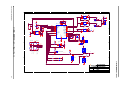
S12ZVML-MINIBRD User Manual:
MC9S12ZVML128 Small Footprint
Board for Sensorless Motor Control
Document Number: S12ZVML-MINIBRD_UM
1.0
04/2014
2
Freescale Semiconductor
About This Book
This document describes the S12ZVML-MINIBRD, the MC9S12ZVML128 small footprint board design,
which is targeted at BLDC and PMSM sensorless motor control applications.
To locate any published updates for this document, refer to freescale.com.
Revision History
Table i. Revision History
Date
Revision
level
April 2014
1.0
Description
Initial release
Page
number(s)
34
Documentation
The MC9S12ZVML128 documentation is available at the web site, http://www.freescale.com/MagniV as
follows:
• Reference manuals — MC9S12ZVML128 modules in detail
• Data sheets — information mainly on the device’s AC, DC, thermal characteristics and package
pin-outs
• Product briefs — device overview
• Application notes — address specific design issues
S12ZVML-MINIBRD Board User Manual, Rev. 1.0
Freescale Semiconductor
3
S12ZVML-MINIBRD Board User Manual, Rev. 1.0
4
Freescale Semiconductor
Chapter 1 Introduction
1.1
1.2
Board Features . . . . . . . . . . . . . . . . . . . . . . . . . . . . . . . . . . . . . . . . . . . . . . . . . . . . . . . . . 8
Board Jumper Configuration . . . . . . . . . . . . . . . . . . . . . . . . . . . . . . . . . . . . . . . . . . . . . . 11
Chapter 2 Board Interface Description
2.1
2.2
2.3
2.4
2.5
2.6
J1 LIN Connector . . . . . . . . . . . . . . . . . . . . . . . . . . . . . . . . . . . . . . . . . . . . . . . . . . . . . . . 13
J9 USB Connector . . . . . . . . . . . . . . . . . . . . . . . . . . . . . . . . . . . . . . . . . . . . . . . . . . . . . . 13
J2 MCU Digital Pin Header . . . . . . . . . . . . . . . . . . . . . . . . . . . . . . . . . . . . . . . . . . . . . . . 14
J4 MCU Analog Pin Header . . . . . . . . . . . . . . . . . . . . . . . . . . . . . . . . . . . . . . . . . . . . . . 14
J7 MCU SCI Port Header . . . . . . . . . . . . . . . . . . . . . . . . . . . . . . . . . . . . . . . . . . . . . . . .14
JP1, JP2, JP3 Motor Terminal Pins . . . . . . . . . . . . . . . . . . . . . . . . . . . . . . . . . . . . . . . . . 14
Chapter 3 Design Consideration
3.1
3.2
3.3
3.4
3.5
3.6
Power Supply . . . . . . . . . . . . . . . . . . . . . . . . . . . . . . . . . . . . . . . . . . . . . . . . . . . . . . . . . 15
MCU Related Circuity . . . . . . . . . . . . . . . . . . . . . . . . . . . . . . . . . . . . . . . . . . . . . . . . . . . 15
Charge Pumps . . . . . . . . . . . . . . . . . . . . . . . . . . . . . . . . . . . . . . . . . . . . . . . . . . . . . . . . . 15
Load Current Sense . . . . . . . . . . . . . . . . . . . . . . . . . . . . . . . . . . . . . . . . . . . . . . . . . . . . 16
BDM Interface . . . . . . . . . . . . . . . . . . . . . . . . . . . . . . . . . . . . . . . . . . . . . . . . . . . . . . . . . 16
OSBDM Interface . . . . . . . . . . . . . . . . . . . . . . . . . . . . . . . . . . . . . . . . . . . . . . . . . . . . . . 16
Chapter 4 Board Electrical Characteristics
Chapter 5 Board Quick Start Guide
5.1
5.2
5.3
5.4
5.5
5.6
Download the S12ZVML-MINIBRD Support Package . . . . . . . . . . . . . . . . . . . . . . . . . . . 19
Software Tool Chain Set-up . . . . . . . . . . . . . . . . . . . . . . . . . . . . . . . . . . . . . . . . . . . . . . . 19
5.2.1 BLDC Motor Control Software Package . . . . . . . . . . . . . . . . . . . . . . . . . . . . . . . 19
5.2.2 CodeWarrior . . . . . . . . . . . . . . . . . . . . . . . . . . . . . . . . . . . . . . . . . . . . . . . . . . . . 20
5.2.3 FreeMASTER . . . . . . . . . . . . . . . . . . . . . . . . . . . . . . . . . . . . . . . . . . . . . . . . . . .20
Hardware Set-up . . . . . . . . . . . . . . . . . . . . . . . . . . . . . . . . . . . . . . . . . . . . . . . . . . . . . . . 20
MCU Code Download and Debug . . . . . . . . . . . . . . . . . . . . . . . . . . . . . . . . . . . . . . . . . . 20
Run and Stop Motor Using External Interface . . . . . . . . . . . . . . . . . . . . . . . . . . . . . . . . . 21
Control Motor Using FreeMASTER tool . . . . . . . . . . . . . . . . . . . . . . . . . . . . . . . . . . . . . . 21
Chapter 6 References
Chapter 7 Acronyms
Chapter 8 S12ZVML-MINIBRD Schematic
Freescale Semiconductor
5
6
Freescale Semiconductor
Introduction
Chapter 1 Introduction
This user manual introduces the S12ZVML-MINIBRD board, which represents the MC9S12ZVML128
small footprint board design.
The MC9S12ZVML128 [3.] integrates a 16-bit microcontroller, an automotive voltage regulator, a LIN
interface and a gate driver unit, in order to drive six external MOSFETs.
The S12ZVML-MINIBRD board is designed for a 3-phase BLDC and PMSM sensorless motor control
application. The board can be used for other applications requiring load switching and load current
monitoring as well. An application can be controlled using LIN and FreeMASTER [4.].
For more information on BLDC sensorless applications, see AN4704 [7.].
S12ZVML-MINIBRD Board User Manual, Rev. 1.0
Freescale Semiconductor
7
Introduction
1.1
Board Features
The board was designed to demonstrate the minimal hardware configuration needed for a 3-phase BLDC
and PMSM sensorless motor control application to achieve minimum board size. The board features are
as follows, see Figure 1-1 and Figure 1-2:
•
•
•
•
•
•
•
•
•
•
•
•
•
MC9S12ZVML128 MCU
power supply voltage in the range of -25 V to +25 V, nominal +12 V
reverse battery protection
load current in range of -10 A to +10 A
load current monitoring
boost circuitry designed to allow driving Vgs = 10 V MOSFETs from a +3.5 V power supply
on-board charge pumps to allow driving the high side MOSFETs
analog and digital inputs for target application control and monitoring
FreeMASTER enabled
LIN enabled
BDM enabled
OSBDM enabled:
— download and debug MCU code
— virtual serial line (USB to SCI)
board size of 5 cm x 9 cm:
— MC9S12ZVML128 related part size of 5 cm x 5 cm
— OSBDM related part size of 5 cm x 4 cm
The on-board OSBDM module allows the user to download and debug code using the CW10.5 tool [5.]
without the need of a P&E Micro USB Multilink.
The FreeMASTER tool allows the user to control the on-board application via the PC USB line.
S12ZVML-MINIBRD Board User Manual, Rev. 1.0
8
Freescale Semiconductor
Introduction
Digital!
Input!/!Output!
OSBDM!Module
User!LED BDM
Serial!
Communication
Interface
LIN
3"phase!MOSFET!Bridge
with!Decoupling!Capacitor!and
Load!Current!Sense!Resistor
MC9S12ZVML128!MCU!
with!
Load!Current!Sense!Circuit
Load!Terminals
Analog!/!Digital!Input!
Figure 1-1. The S12ZVML-MINIBRD board top side view
S12ZVML-MINIBRD Board User Manual, Rev. 1.0
Freescale Semiconductor
9
Introduction
Reverse!Battery!Protection
Boost!Circuit
Figure 1-2. The S12ZVML-MINIBRD board bottom side view
S12ZVML-MINIBRD Board User Manual, Rev. 1.0
10
Freescale Semiconductor
Introduction
1.2
Board Jumper Configuration
See Table 1-1 and Figure 1-3 for proper jumper configuration.
Table 1-1. S12ZVML-MINIBRD Board Configuration
Jumper
MCU pin
J5
PP0
EVDD1
ECLK
J6
J8
Function
Default placement
MCU PP0 output:
- ECLK, not placed
- EVDD1, placed
Placed
PS2
RxD1
Select MCU RxD1 pin connection:
- USB OSBDM, placed, pins 1-2
- J7 SCI PORT, placed, pins 2-3
Placed, pins 1-2
PS3
TxD1
Select MCU TxD1 pin connection:
- USB OSBDM, placed, pins 1-2
- J7 SCI PORT, placed, pins 2-3
Placed, pins 1-2
J5!PP0
J6!PS2
J8!PS3
Figure 1-3. S12ZVML-MINIBRD board jumper position and setting
S12ZVML-MINIBRD Board User Manual, Rev. 1.0
Freescale Semiconductor
11
Introduction
S12ZVML-MINIBRD Board User Manual, Rev. 1.0
12
Freescale Semiconductor
Board Interface Description
Chapter 2 Board Interface Description
This chapter summarizes the on-board connectors and header pin-outs, signal meanings, and MCU pins
assignments.
2.1
J1 LIN Connector
The board is supplied using the LIN connector J1, see Table 2-1 for the connector pin-outs. The MCU is
configured as a LIN Slave node.
Table 2-1. J1 LIN connector
Interface Pin
Signal Name
MCU Signal
Description
Direction
1
GND
-
Ground
-
2
GND
-
Ground
-
3
VSUP
-
Power Supply
-
4
LIN
RXD1/TXD1
LIN bus
Bidirectional
The J1 LIN connector opposite uses MOLEX 39-01-2040 with pins MOLEX 39-00-0039.
2.2
J9 USB Connector
The USB line is used for on-board OSBDM module communication with the PC. The OSBDM module is
used for MCU code download and debug using the CW 10.5 tool, as well as a virtual serial port when using
the FreeMASTER tool to control the user application.
The interface uses a USB 2.0 B type connector, see Table 2-2.
Table 2-2. J9 USB connector
Interface Pin
Signal Name
MCU Signal
Description
Direction
1
VBUS
-
USB Power Supply
-
2
D-
RXD0/TXD0
Data –
Bidirectional
3
D+
RXD0/TXD0
Data +
Bidirectional
4
GNDB
-
USB Ground
-
S12ZVML-MINIBRD Board User Manual, Rev. 1.0
Freescale Semiconductor
13
Board Interface Description
2.3
J2 MCU Digital Pin Header
The MCU PT1 digital pin can be used for an application control and monitoring, see Table 2-3.
Table 2-3. 2 MCU PT1 pin header
Interface Pin
Signal Name
MCU Signal
Description
Direction
1
VDDX
-
VDDX output (+5V)
-
2
-
PT1/IOC1
PT1 pin input / output
Bidirectional
3
GND
-
GND
-
2.4
J4 MCU Analog Pin Header
The MCU PAD3 analog pin can be used for an application control and monitoring, see Table 2-4.
Table 2-4. J4 MCU PAD3 pin header
Interface Pin
Signal Name
MCU Signal
Description
Direction
1
VDDX
-
VDDX output (+5V)
-
2
-
PAD3/AN0_3
PAD3 pin input
Input
3
GND
-
GND
-
2.5
J7 MCU SCI Port Header
The J7 allows to connect board external device using the MCU SCI module, see Table 2-5. The MCU SCI
port availability depends on the J6 and J8 configuration, see Table 1-1.
Table 2-5. J7 MCU SCI port header
Interface Pin
Signal Name
MCU Signal
Description
Direction
1
VDDX
-
VDDX output (+5V)
-
2
RXD
RXD1
Connection depending on J6 configuration
Input
3
TXD
TXD1
Connection depending on J8 configuration
Output
4
GNDB
-
Ground
-
2.6
JP1, JP2, JP3 Motor Terminal Pins
The JP1, JP2, JP3 are the phases half-bridge outputs. The terminals are used to connect the controlled load,
for example BLDC, PMSM motor.
S12ZVML-MINIBRD Board User Manual, Rev. 1.0
14
Freescale Semiconductor
Design Consideration
Chapter 3 Design Consideration
The S12ZVML-MINIBRD board schematic can be found in Chapter 8, “S12ZVML-MINIBRD
Schematic".
3.1
Power Supply
The board is supplied using the J1 LIN connector, see Table 1-1 for the connector pin-outs. The board
nominal power supply voltage equals +12 V. The board sustains negative voltages up to -25 V due to M1
reverse battery protection.
The power supply line is decoupled by C5. The value of the capacitor is dependent on the required power
supply voltage ripple, when board load, for example BLDC / PMSM motor, is PWM driven. The goal is
to achieve minimum power supply voltage ripple to reduce board electromagnetic emissions.
An on-board boost circuit, L1, D1, C1, C2 allows controlling the Vgs = 10 V MOSFETs starting from a
+3.5V power supply voltage. The boost circuitry is turned ON and controlled by the MCU GDU boost
controller module when the power supply voltage drops below +10 V. The boost circuitry is optimized for
operation at 520 kHz with the MCU GDU boost controller duty cycle set to 75% and the L1 inductor
current limit at 750 mA. The boost snubber circuitry R3 and C6 is included to dump the oscillations
appearing when the boost transistor is switched.
The on-board D7 +2.47 V voltage reference sets the ADC voltage, when the load current equals 0 A, see
Table 3-1.
3.2
MCU Related Circuity
The MCU is supplied with VSUP pin. The MCU on-chip +5 V voltage regulator generates the voltage for
the MCU digital and analog circuitry. The decoupling capacitors C7, C8, C9 reduce noise on the power
supply lines. The MCU analog power supply line noise is reduced using the ferrite bead L2 and capacitor
C12.
The GDU drives the Q1, Q2, Q3, Q4, Q5, Q6 MOSFETs configured in a 3-phase bridge unit with phase
outputs JP1, JP2, JP3. The GDU is supplied by the on-chip +11 V VLS regulator decoupled by C13, C14,
C18 and C19. Whenever the power supply voltage drops below +10 V, the boost circuitry starts to operate
and the VSUP voltage is maintained at +10 V. The boost circuitry allows driving the Vgs = 10 V MOSFETs
starting from a +3.5 V power supply voltage.
The J2 digital PT1 pin signal and J4 analog PAD3 signal can be used for an application monitoring and
control.
The PP0 pin controls the D8 LED. The PP0 shares the MCU clock output ECLK as well.
The J7 allows to connect board external device using the MCU SCI module. The availability depends on
J6 and J8 jumper header settings, see Table 1-1.
3.3
Charge Pumps
There are four charge pumps to supply the GDU HSDs modules.
S12ZVML-MINIBRD Board User Manual, Rev. 1.0
Freescale Semiconductor
15
Design Consideration
The D4, C15, D5, C16, D6, C17 charge pumps are driven by the phase voltages. They supply the GDU
HSDs when the PWM duty cycle is within minimal and maximal limits.
The D2, D3, C3, C4 charge pump is driven by the MCU VCP pin. This is used to supply the GDU HSDs
when the PWM duty cycle is either 0% or 100%.
3.4
Load Current Sense
The load current sense circuitry is designed to measure load current in both directions. This is useful when
the attached motor is controlled in dynamo mode as well.
The load current is sensed by R20 and amplified by the on-chip amplifier AMP0. The R19, R22, and C20
reduce the sense line noise. The R28 and C23 shape the AMP0 signal.
The load current conversion slope theoretically equals 0.125 V/ 1 A, see Table 3-1.
Table 3-1. Load current sense
3.5
Load current [A]
MCU AN0 pin voltage [V]
10
3.72
0
2.47
-10
1.22
BDM Interface
The on-board J3 BDM connector allows a download and debug of the code in the MCU using CodeWarrior
10.5 and P&E Micro USB Multilink.
The BDM interface can be used for application control using FreeMASTER as well.
3.6
OSBDM Interface
The on-board OSBDM interface allows a download and debug of the code in the MCU without any
additional debugging hardware. The P&E Micro USB Multilink is not needed.
The OSBDM interface can be used as a board virtual serial port for FreeMASTER based application
control.
S12ZVML-MINIBRD Board User Manual, Rev. 1.0
16
Freescale Semiconductor
Board Electrical Characteristics
Chapter 4 Board Electrical Characteristics
The electrical characteristics in Table 4-1 apply to operation at 25 °C.
Table 4-1. Electrical Characteristics
Characteristic
Maximal power supply voltage range, J1 pin3
Operating power supply voltage range, J1 pin3
Power supply current consumption (2)
J2 pin2, J4 pin2, J7 pin2, J7 pin3 voltage range
1MCU
(1)
Symbol
Min
Typ
Max
Units
VDCMAX
-25
-
25
V
VDC
3.5
12
20
V
IDC
-
20
-
mA
VPER
0
–
5
V
boost option enabled. When MCU boost option disabled, VDC_MIN = 6V.
at 12 V power supply. MCU flash memory erased.
2Measured
S12ZVML-MINIBRD Board User Manual, Rev. 1.0
Freescale Semiconductor
17
Board Electrical Characteristics
S12ZVML-MINIBRD Board User Manual, Rev. 1.0
18
Freescale Semiconductor
Board Quick Start Guide
Chapter 5 Board Quick Start Guide
This chapter describes how to set-up the S12ZVML-MINIBRD board to control the BLDC motor, see
Figure 5-1.
Figure 5-1. S12ZVML-MINIBRD set-up
5.1
Download the S12ZVML-MINIBRD Support Package
Visit the MagniV S12ZVML-MINIBRD related Freescale’s web pages [2.]. Navigate the “Jump Start Your
Design” section and download the latest version of documentation and software package.
5.2
5.2.1
Software Tool Chain Set-up
BLDC Motor Control Software Package
Run the “S12ZVML-MINIBRD_BLDC_Sensorless_CW_IDE.exe” file and install and BLDC Motor
Control project “S12ZVML-MINIBRD_BLDC_Sensorless_CW_IDE” and the Automotive Math and
Motor Control Library Set [6.].
S12ZVML-MINIBRD Board User Manual, Rev. 1.0
Freescale Semiconductor
19
Board Quick Start Guide
5.2.2
CodeWarrior
The CodeWarrior tool enables development, download and debug code in on-board MCU. Visit the
CodeWarrior [5.] web page and install the free trial CW 10.5 version on your PC. Once the CW 10.5 is
installed, import the “S12ZVML-MINIBRD_BLDC_Sensorless_CW_IDE” project in CW 10.5:
1. Open CW 10.5
2. Go to the “Help” folder and choose “Search”
3. Type in the search window the key words “Import existing project”
4. Follow the instructions to import the “S12ZVML-MINIBRD_BLDC_Sensorless_CW_IDE”
project
For additional information:
1. Go to the “Help” folder and choose “Documentation”
2. Open the “Getting Started” folder
3. Download “Microcontroller V10.x Quick Start”
5.2.3
FreeMASTER
Install the free of charge FreeMASTER tool on your PC available at [4.]
5.3
Hardware Set-up
The S12ZVML-MINIBRD kit contains:
1. S12ZVML-MINIBRD board
2. J1 power supply cable, length 1 m
3. USB A male to B male cable, length 2 m
Follow instructions for board hardware set-up:
1. Check the S12ZVM-MINIBRD jumper settings, see Table 1-1, Figure 1-3.
1. Connect BLDC motor, type LINIX 45ZWN24-90-B, with the S12ZVML-MINIBRD, pins JP1,
JP2, JP3, see Figure 1-1 and Figure 5-1
2. Connect the power supply cable with the S12ZVML-MINIBRD, J1 LIN connector
3. Connect the power supply cable with the 12 V / 4 A power supply. The red wire goes to the positive
terminal, the black wire (white wire) goes to the negative terminal
4. Turn ON the power supply
5. Connect the PC and S12ZVML-MINIBRD terminal J9 with a USB2.0 cable, type A to B
5.4
MCU Code Download and Debug
Create an OSBDM download profile, see the CW 10.5 project “Run” tab “Debug configuration”. Go to
the “Run” tab, choose “Debug” and download code to the S12ZVML MCU using the on-board OSBDM
module. Once the code is downloaded, go to “Run” and select “Resume” to run the code in MCU.
S12ZVML-MINIBRD Board User Manual, Rev. 1.0
20
Freescale Semiconductor
Board Quick Start Guide
5.5
Run and Stop Motor Using External Interface
The motor can be controlled using the J2 header. Run motor by placing the jumper short bar to J2, pin 1-2.
5.6
Control Motor Using FreeMASTER tool
The motor can be controlled using the FreeMASTER tool, see Figure 5-2:
1. Go to CodeWarrior 10.5 “Run” folder and select “Disconnect” to release the board USB channel.
The USB communication channel will be used by FreeMASTER tool now
2. Place jumper short bar J2, pins 2-3
3. Search for the USB virtual port in the PC Device Manager
4. Open the FreeMASTER control page “S12ZVML-MINIBRD_BLDC_Sensorless.pmp” located in
the “S12ZVML-MINIBRD_BLDC_Sensorless_CW_IDE” folder
5. Go to the Project/Options comm tab and set the USB virtual port number, and the communication
speed 9600 kBd, see Figure 5-3
6. Run the communication by pressing CTRL+K
7. Enter the required BLDC motor rotation speed in the “Required Speed RPM” variable, range from
1500 rpm to 8000 rpm at 12 V power supply
8. Run / Stop motor by variable “Turn ON/OFF”
9. Analyze motor behavior in the “Speed Scope” window
10. Monitor the DC BUS Voltage (module power supply voltage) and DC BUS Current (motor current)
For more information on BLDC sensorless applications, see AN4704 [7.].
S12ZVML-MINIBRD Board User Manual, Rev. 1.0
Freescale Semiconductor
21
Board Quick Start Guide
Figure 5-2. FreeMASTER control page
Figure 5-3. FreeMASTER options communication tab
S12ZVML-MINIBRD Board User Manual, Rev. 1.0
22
Freescale Semiconductor
Board Quick Start Guide
Figure 5-4. FreeMASTER options map file tab
S12ZVML-MINIBRD Board User Manual, Rev. 1.0
Freescale Semiconductor
23
Board Quick Start Guide
S12ZVML-MINIBRD Board User Manual, Rev. 1.0
24
Freescale Semiconductor
References
Chapter 6 References
1.
2.
3.
4.
5.
6.
7.
MagniV family web page, www.freescale.com/MagniV
S12ZVML-MINIBRD web page, www.freescale.com/S12ZVML-MINIBRD
MC9S12ZVM Family Reference Manual, www.freescale.com
FreeMASTER Run-Time Debugging Tool, www.freescale.com/freemaster
CodeWarrior Development Tools, www.freescale.com/codewarrior
Automotive Math and Motor Control Library Set, www.freescale.com/AutoMCLib
AN4704, 3-phase Sensorless BLDC Motor Control Kit with MC9S12ZVM, www.freescale.com
S12ZVML-MINIBRD Board User Manual, Rev. 1.0
Freescale Semiconductor
25
References
S12ZVML-MINIBRD Board User Manual, Rev. 1.0
26
Freescale Semiconductor
Acronyms
Chapter 7 Acronyms
ADC
Analog to Digital Converter
BLDC
Brushless DC Motor
CW
CodeWarrior Tool
HSD
High Side Driver
LIN
Local Interconnect Network
MCU
Microcontroller Unit
PC
Personal Computer
PWM
Pulse Width Modulation
PMSM
Permanent Magnet Synchronous Motor
USB
Universal Serial Bus
S12ZVML-MINIBRD Board User Manual, Rev. 1.0
Freescale Semiconductor
27
Acronyms
S12ZVML-MINIBRD Board User Manual, Rev. 1.0
28
Freescale Semiconductor
4
3
2
1
SCHEMATIC REVISIONS
Zone
All
D
Rev
X1
A
A1
Description
Date
9.12.2013
19.12.2013
12.02.2014
Initial version
First release
BOM Change
Revised
PCh
PCh
Simon Xu
D
S12ZVML-MINIBRD Board User Manual, Rev. 1.0
C
C
B
B
Freescale Semiconductor RCSC
Chapter 8 S12ZVML-MINIBRD Schematic
Freescale Semiconductor
5
1. maje 1009
765 61 Roznov p. R. Czech republic, Europe
S12ZVML_MINIBRD
A
5
4
3
Drawn by:
PCh
Page Title:
Approved:
PCh
Size
A
Document Number
Date:
Monday, March 31, 2014
A
Info
Rev
A1
SCH-28219 PDF: SPF-28219
2
Sheet
1
of
1
3
29
S12ZVML-MINIBRD Schematic
This document contains information proprietary to Freescale Semiconductor and shall not be used for
engineering design, procurement or manufacture in whole or in part without the express written permission
of Freescale Semiconductor.
ICAP Classification:
FCP: ____
FIUO: ____ PUBI: X
Designer:
Drawing Title:
PCh
4
3
J1
4
3
2
1
1
D4
S1
7
S2
D3
D2
4
G
C3
0.01UF
D1
VCP
VSUP
+
C1
68UF
/25V
C2
0.22uF /25V
D
D3
BAS16H
R1
1.0K
1
R3
1.0K
VSUP BOOST
C6
1000PF
C
M1
FDS6681Z
BST
C5
1000UF
25V
C4
0.22uF
A
S3
5
LIN
Board Power Supply
(-25V, +25V)
CP
R2
100K
+
C
3
D1
MBRS260T3G
A
C
100uH
D2
BAS16H
2
6
CON PLUG 4
D
A
LIN
8
2
L1
SRU8043-101Y
1
2
REVERSE BATTERY PROTECTION
GND_BST
VBS CHARGE PUMP
C8 10UF/16V
VDDX
C9 0.22uF
LIN
D9
MMBZ27VCLT1
1
C11 0.22uF
VDDA
0
9
BKGD
/RST
2
54
R29
BKGD
/RST
18
J3
A
1
3
5
2
4
6
/RST
VDDX
VLS
VCP
CP
R5
0
Q2
SQD50N03
1
HG1
R6
0
Q3
SQD50N03
1
HG2
R11
C23
10pF
DNP
0
Q4
SQD50N03
1
R14
0
LS0
HDR 1X1
C17
0.22uF
HDR 1X1
D6
BAS16H
R12
VLS
0
Q5
SQD50N03
1
LG1
R15
LS1
0
4
4
VLS
JP3
1
C
C16
0.22uF
D5
BAS16H
LG0
LG2
LS2
HDR 1X1
0
VBS2
B
R13
0
Q6
SQD50N03
1
LG2
R16
0
3
C19 0.22uF
C15
0.22uF
R9
HS2
JP2
1
C
C18 0.22uF
0
VBS1
3
R8
HS1
JP1
1
VBS0
A
0
HS0
3
R7
3
LG0
LS0
3
HS2
HG2
VBS2
VLS2
LG2
LS2
AN0_0/AMP0/KWAD0/PAD0
AN0_1/AMPM0/KWAD1/PAD1
AN0_2/AMPP0/KWAD2/PAD2
AN0_3/KWAD3/PAD3
AN0_4/KWAD4/PAD4
AN1_0/AMP1/KWAD5/PAD5
(SS)/AN1_1/AMPM1/KWAD6/PAD6
VRL/AN1_2/AMPP1/KWAD7/PAD7
VRH/AN1_3/KWAD8/PAD8
BCTL
MODC/BKGD
RESET
TEST
21
22
23
24
25
26
27
28
29
R17 40K
R18 2.2K
LS2
R19 1.0K
C21
R25
1.0K
R21 2.2K
Freescale Semiconductor RCSC
R22 1.0K
1. maje 1009
765 61 Roznov p. R. Czech republic, Europe
R24 1.0K
VDDA
0.01UF
TP2
J4
VDDX
1
2
3
~2.47V
R26
10K
Cathode
C22
0.22uF
Freescale Semiconductor
FB
BDM
HDR_1X3
Anode
D7
LM4041DIDBZTG4
4
R20
0.01
C20
680PF
DNP
R23
40K
HDR 2X3
5
4
D4
BAS16H
HS2
HG2
VBS2
4
LG1
LS1
38
39
40
41
42
43
Q1
SQD50N03
A
HS1
HG1
VBS1
VLS1
LG1
LS1
0
1
3
3
BKGD
HS1
HG1
VBS1
R4
HG0
C14 0.22uF
R28 43K DNP
EP_PAD
11
14
VCP
CP
VSUP
BST
VSSB
VSSX1
16
12
13
65
VSUP
BST
GND_BST
PE1/XTAL
PE0/EXTAL
63
55
56
PT0/IOC0/(PWM3)/(MISO)/(RXD0)
PT1/IOC1/(PWM4)/(MOSI)/(TXD0)/LPDR1/PTURE
PT2/IOC2/(PWM5)/(SCK)
PT3/IOC3/(SS)
VSSA
HDR_1X3
50
51
52
53
VSS1
VSS2
R10 1.0K
31
VDDX
49
48
47
46
45
44
4
30
VDDA
62
17
58
VDDF
VDDX1
VDDX2
PP0/EVDD1/KWP0/(PWM0)/ECLK/FAULT5/XIRQ
PP1/KWP1/(PWM1)/IRQ
PP2/KWP2/(PWM2)
57
19
1
2
3
HS0
HG0
VBS0
C13 10UF/16V
HS0
HG0
VBS0
VLS0
LG0
LS0
J2
B
VLS
37
36
35
34
33
32
4
LED_GREEN
61
60
59
15
3
J5
HDR 1X2 TH
PTUT0/(LPRXD)/RXCAN/RXD1/KWS0/PS0
PTUT1/(LPTXD)/TXCAN/TXD1/KWS1/PS1
MISO/(RXD1)/KWS2/PS2
MOSI/(TXD1)/DBGEEV/KWS3/PS3
PDOCLK/SCK/KWS4/PS4
PDO/SS/KWS5/PS5
10
C
A
HD
VLS_OUT
A
R30
1.0K
D8
LIN
LGND
0.22uF
2
3
4
5
6
7
8
20
U1
PC9S12ZVML12MKH
1
64
C
C
DNP
2
RXD1
TXD1
C12
TP1
C24
220PF
/50V
3
VDD
C
L2
1000 OHM
C10 0.22uF
1
2
S12ZVML-MINIBRD Board User Manual, Rev. 1.0
VDDX
C7 0.22uF
This document contains information proprietary to Freescale Semiconductor and shall not be used for
engineering design, procurement or manufacture in whole or in part without the express written permission
of Freescale Semiconductor.
ICAP Classification:
FCP: ____
FIUO: ____ PUBI: X
Drawing Title:
Designer:
PCh
S12ZVML_MINIBRD
1
R27
10K
Drawn by:
PCh
Page Title:
Approved:
PCh
Size
B
Document Number
Date:
Monday, March 31, 2014
2
MCU
Rev
A1
SCH-28219 PDF: SPF-28219
Sheet
1
2
of
3
A
S12ZVML-MINIBRD Schematic
30
5
Freescale Semiconductor
5
4
3
2
1
+5V_SW
+5V_SW
U2
74LVC1T45
5
DIR
3
2
VDDX
1
6
VCCA
VCCB
A
GND
VDDX
C25
10UF
/16V
4
B
J6
R31
D
+5VU
R32
1.0K
1
2
3
0
RXD1
C26
0.22uF
D
HDR_1X3
DNP
+5V_SW
U3
74LVC1T45
+5VU
C27
0.22uF
C28
10UF
/16V
5
C29
0.22uF
R34
10K
R39 2.4K
BRD_ID1
R40
10K
R41
10K
U6
MIC2026-1YM
2
3
+5V_SW
8
5
C31
10UF
/16V
TRESET_OUT
FLGA
ENA
FLGB
ENB
OUTA
IN
OUTB
GND
1
4
PTB0/MISO2/ADP0
PTB1/MOSI2/ADP1
PTB2/SPSCK2/ADP2
PTB3/SS2/ADP3
PTB4/KBIP4/ADP4
PTB5/KBIP5/ADP5
40
41
42
43
1
44
BRD_REV0
BRD_REV1
BRD_REV2
J8
PTC0/SCL
PTC1/SDA
PTC2
PTC3/TxD2
PTC4
PTC5/RxD2
R36
PTE0/TxD1
PTE1/RxD1
PTE2/TPM1CH0
PTE3/TPM1CH1
PTE4/MISO1
PTE5/MOSI1
PTE6/SPSCK1
PTE7/SS1
PTF0/TPM1CH2
PTF1/TPM1CH3
PTF4/TPM2CH0
PTF5/TPM2CH1
8
9
10
11
12
13
14
15
7
6
29
30
33
U_IRQ*
U_RESET*
U_BKGD*
2
3
36
PTD0/ADP8/ACMP+
PTD1/ADP9/ACMPPTD2/KBIP2/ACMPO
C32
0.22uF
+5V_SW
21
22
34
35
37
38
R44
20
18
19
C34
0.22uF
Y1
1
4MHz
S2
2
3
4
1
S1
33
33
1000 OHM
C37
1000PF
VDDX
2
+5VU
R58
3.3K
E
+5VU
U7
DDTA113ZCA
R1
J11
R60
10K
ENABLE BOOTLOADER
1 B
Pull-Down
0
1.3K
3.3K
5.6K
B
+5V_SW
1
2
3 C
ID1
2
R61
0
HDR 1X2 TH
/RST
C
A
R2
A
2
C
3
E
D11
LED_PWR
R1
R64
1.0K
B
C
LED_GREEN
C
U8
DDTC113ZCA
D10
LED_STATUS
1
R1
+5VU
R63
1.0K
R62
47.0
1
3
TRESET_IN
B
Pull-Up
10K
10K
10K
10K
J9
USB_TYPE_B
L4
R59
10K
ID0
0
-D
+D
G
V
R2
R57
0
R53
10K
2
4
6
HDR 2X3
B
ID
0
1
2
3
R45
R46
L3
1000 OHM
1
R56
10K
DNP
BRD_REV
001
C36
18PF
J10
BRD_ID1
BRD_ID0
R55
10K
2
C35
18PF
OSBDM BDM
1
3
5
BRD_REV2
BRD_REV1
BRD_REV0
R54
10K
10M
+5VU
C33
10UF
/16V
+5VU
R52
10K
R51
10K
BKGD
C
VUSB33
USBDN
USBDP
+5VU
R50
10K
R42
0
TBGND
+5VSW_FAULT
+VTRG_FAULT
BOARD ID
R49
10K
4
B
2
R48
10K
DNP
A
GND
4
R47
10K
DNP
VDDX
1
6
VCCA
VCCB
R43
4.7K
OSBDM_USB_DN
OSBDM_USB_DP
+5VU
BOARD REV
DIR
3
2
TBGND_IN
TBGND_OUT
TBGND_EN
32
17
39
C
PTG0/KBIP0
PTG1/KBIP1
PTG2/KBIP6
PTG3/KBIP7
PTG4/XTAL
PTG5/EXTAL
IRQ/TPMCLK
RESET
BKGD/MS
SCI PORT
TXD1
HDR_1X3
U5
74LVC1T45
5
4
5
6
7
+5V
RXD
TXD
GND
HDR_1X4
R35
1.0K
1
2
3
0
DNP
+5VU
TPWR
TSTATUS
TRESET_IN
4
B
3
S12ZVML-MINIBRD Board User Manual, Rev. 1.0
23
24
25
26
27
28
+5VSW_EN
+VTRG_EN
BRD_ID0
VDDAD/VREFH
VDD1
R37
10K
VSSAD/VREFL
VSS1
VSSOSC
C30
0.22uF
VCCA
VCCB
A
GND
1
2
3
4
SCI SELECT
31
16
U4
MC9S08JM60CLD
R38
10K
DIR
3
2
R33
10K
J7
VDDX
1
6
U9
DDTC113ZCA
R2
LED_YEL
A
1. maje 1009
765 61 Roznov p. R. Czech republic, Europe
This document contains information proprietary to Freescale Semiconductor and shall not be used for
engineering design, procurement or manufacture in whole or in part without the express written permission
of Freescale Semiconductor.
ICAP Classification:
FCP: ____
FIUO: ____ PUBI: X
Designer:
Drawing Title:
PCh
S12ZVML_MINIBRD
5
4
3
2
Drawn by:
PCh
Page Title:
Approved:
PCh
Size
C
Document Number
Date:
Monday, March 31, 2014
OSBDM
Rev
A1
SCH-28219 PDF: SPF-28219
Sheet
1
3
of
3
31
S12ZVML-MINIBRD Schematic
2
E
Freescale Semiconductor RCSC
A
S12ZVML-MINIBRD Schematic
S12ZVML-MINIBRD Board User Manual, Rev. 1.0
32
Freescale Semiconductor
How to Reach Us:
Home Page:
www.freescale.com
Web Support:
http://www.freescale.com/support
USA/Europe or Locations Not Listed:
Freescale Semiconductor, Inc.
Technical Information Center, EL516
2100 East Elliot Road
Tempe, Arizona 85284
1-800-521-6274 or +1-480-768-2130
www.freescale.com/support
Europe, Middle East, and Africa:
Freescale Halbleiter Deutschland GmbH
Technical Information Center
Schatzbogen 7
81829 Muenchen, Germany
+44 1296 380 456 (English)
+46 8 52200080 (English)
+49 89 92103 559 (German)
+33 1 69 35 48 48 (French)
www.freescale.com/support
Japan:
Freescale Semiconductor Japan Ltd. Headquarters
ARCO Tower 15F
1-8-1, Shimo-Meguro, Meguro-ku,
Tokyo 153-0064
Japan
0120 191014 or +81 3 5437 9125
[email protected]
Asia/Pacific:
Freescale Semiconductor China Ltd.
Exchange Building 23F
No. 118 Jianguo Road
Chaoyang District
Beijing 100022
China
+86 10 5879 8000
[email protected]
Freescale Semiconductor Literature Distribution Center
1-800-441-2447 or +1-303-675-2140
Fax: +1-303-675-2150
[email protected]
Information in this document is provided solely to enable system and
software implementers to use Freescale Semiconductor products. There are
no express or implied copyright licenses granted hereunder to design or
fabricate any integrated circuits or integrated circuits based on the
information in this document.
Freescale Semiconductor reserves the right to make changes without further
notice to any products herein. Freescale Semiconductor makes no warranty,
representation or guarantee regarding the suitability of its products for any
particular purpose, nor does Freescale Semiconductor assume any liability
arising out of the application or use of any product or circuit, and specifically
disclaims any and all liability, including without limitation consequential or
incidental damages. “Typical” parameters that may be provided in Freescale
Semiconductor data sheets and/or specifications can and do vary in different
applications and actual performance may vary over time. All operating
parameters, including “Typicals”, must be validated for each customer
application by customer’s technical experts. Freescale Semiconductor does
not convey any license under its patent rights nor the rights of others.
Freescale Semiconductor products are not designed, intended, or authorized
for use as components in systems intended for surgical implant into the body,
or other applications intended to support or sustain life, or for any other
application in which the failure of the Freescale Semiconductor product could
create a situation where personal injury or death may occur. Should Buyer
purchase or use Freescale Semiconductor products for any such unintended
or unauthorized application, Buyer shall indemnify and hold Freescale
Semiconductor and its officers, employees, subsidiaries, affiliates, and
distributors harmless against all claims, costs, damages, and expenses, and
reasonable attorney fees arising out of, directly or indirectly, any claim of
personal injury or death associated with such unintended or unauthorized
use, even if such claim alleges that Freescale Semiconductor was negligent
regarding the design or manufacture of the part.
Freescale™ and the Freescale logo are trademarks of Freescale
Semiconductor, Inc. All other product or service names are the property of their
respective owners.
© Freescale Semiconductor, Inc. 2014. All rights reserved.
S12ZVML-MINIBRD_UM
Rev. 1.0
04/2014