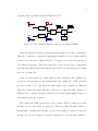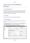
1
FPGA-based, 4-channel, High-speed
Phasemeter for Heterodyne Interferometry
by
Chen Wang
Submitted in Partial Fulfillment of the
Requirements for the Degree
Master of Science
Supervised by
Jonathan D. Ellis
Department of Electrical and Computer Engineering
Arts, Sciences and Engineering
Edmund A. Hajim School of Engineering and Applied Sciences
University of Rochester
Rochester, New York
2013
iii
Biographical Sketch
The author was born in Lucheng, Shanxi, China. He attended Harbin Institute of
Technology, and graduated with a Bachelor of Engineering degree in Measurement,
Control Technique and Instruments in 2011. He began master’s studies in Electrical
Engineering at the University of Rochester in 2011. He pursued his research in
Precision Instrumentation under the direction of Jonathan D. Ellis.
iv
v
Acknowledgments
First of all, I would like to acknowledge my parents for their support to my graduate
studies oversea. I would also like to thank Steven Gillmer, Richard Smith, and other
colleagues in the Precision Instrumentation Group, whose knowledge and assistance
were invaluable contributions to this research. Finally, thank you to Prof. Jonathan
D. Ellis, who provided me the opportunity to work in this field, and gave me the
motivation and inspiration on graduate study and research.
vi
vii
Abstract
A phasemeter is a device for performing phase measurements by extracting the
relative phase between two alternating signals. It is widely used with heterodyne
interferometry to measure displacement. Its performance determines the quality
of entire displacement measurement. The aim of this work is to design a highspeed, high-precision, compact, and economical, user-friendly interface phasemeter
prototype, which could outperform the currently-used commercial phase measurement
solution in the laboratory.
The phasemeter was designed in three crucial parts, which includes detection
and analog signal processing circuitry, digital signal processing algorithm of phase
measurement, and Ethernet transmission. The detection and processing circuitry
employed a large active area photodiode for detecting the incident laser beam with
high spatial sensitivity for differential wavefront sensing, and analog signal processing
circuits, such as filters, gain, buffers to optimize the analog signal.
The phase
measurement algorithm was implemented in an FPGA board with high processing
speed, flexible and parallel performance. The Ethernet transmission was based on user
datagram protocol (UDP), whose transmitting end was implemented by an embedded
system in the FPGA and receiving end was implemented by a Matlab xPC Target.
This work has achieved a phasemeter prototype with an ability to be utilized in
differential wavefront sensing, high phase processing speed, and user-friendly, easily
viii
accessible interface, which is competent to replace the currently-used commercial
phase measurement solution in the laboratory.
ix
Contributors and Funding Sources
This work was supervised by a dissertation committee consisting of Professor
Jonathan D. Ellis (advisor) of the Department of Mechanical Engineering and The
Institute of Optics, Professors Qiang Lin and Tolga Soyata of the Department
of Electrical and Computer Engineering, and Professor Nick Vamivakas of The
Institute of Optics. All work for the dissertation was completed independently by the
student. The graduate study and research were supported, in part, by the National
Institute of Standards and Technology (NIST) under cooperative agreement number
70NANB12H186.
x
xi
Table of Contents
Biographical Sketch
Acknowledgments
Abstract
iii
v
vii
Contributors and Funding Sources
ix
List of Figures
xv
1 Introduction
1
1.1 Overview . . . . . . . . . . . . . . . . . . . . . . . . . . . . . . . . . .
1
1.2 Zero-crossing Algorithm . . . . . . . . . . . . . . . . . . . . . . . . .
6
1.3 Phase-locked Loop based Lock-in Detection Algorithm . . . . . . . .
9
1.4 Single-bin DFT Algorithm . . . . . . . . . . . . . . . . . . . . . . . .
20
1.5 Motivation and Goals . . . . . . . . . . . . . . . . . . . . . . . . . . .
24
2 Detection and Processing Board Design
2.1 Detection and Processing Principles . . . . . . . . . . . . . . . . . . .
29
30
xii
2.2
Device Selection . . . . . . . . . . . . . . . . . . . . . . . . . . . . . .
40
2.3
Printed Circuit Board Design . . . . . . . . . . . . . . . . . . . . . .
51
2.4
Verification Measurement . . . . . . . . . . . . . . . . . . . . . . . . .
57
3 Digital Signal Processing Module Design
63
3.1
FPGA Introduction . . . . . . . . . . . . . . . . . . . . . . . . . . . .
63
3.2
Hardware Introduction . . . . . . . . . . . . . . . . . . . . . . . . . .
66
3.3
Software Introduction . . . . . . . . . . . . . . . . . . . . . . . . . . .
68
3.4
Model Design . . . . . . . . . . . . . . . . . . . . . . . . . . . . . . .
70
3.5
Simulink Simulation . . . . . . . . . . . . . . . . . . . . . . . . . . .
82
3.6
FPGA Implementation . . . . . . . . . . . . . . . . . . . . . . . . . .
87
3.7
Verification . . . . . . . . . . . . . . . . . . . . . . . . . . . . . . . .
91
4 Measurement Data Transmission
93
4.1
User Datagram Protocol . . . . . . . . . . . . . . . . . . . . . . . . .
93
4.2
Transmitting End Implementation . . . . . . . . . . . . . . . . . . . .
99
4.3
Receiving End Implementation
4.4
New-built Phasemeter System Test . . . . . . . . . . . . . . . . . . . 110
5 Conclusions and Future Work
. . . . . . . . . . . . . . . . . . . . . 106
115
5.1
Detection and Processing Board . . . . . . . . . . . . . . . . . . . . . 115
5.2
Digital Signal Processing based on FPGA . . . . . . . . . . . . . . . 116
5.3
UDP Transmission . . . . . . . . . . . . . . . . . . . . . . . . . . . . 117
5.4
Future Work . . . . . . . . . . . . . . . . . . . . . . . . . . . . . . . . 118
xiii
Bibliography
123
A Appendix
129
xiv
xv
List of Figures
1.1 A phase difference ϕ between two alternating input signals . . . . . .
2
1.2 Classical stand-alone instrument and virtual instrument phasemeters
3
1.3 Photolithography stepper machine with interferometers . . . . . . . .
5
1.4 The configuration of a displacement measurement interferometer . . .
5
1.5 The schematic diagram of the zero-crossing algorithm . . . . . . . . .
7
1.6 Exclusive OR operation of two logic signals . . . . . . . . . . . . . . .
8
1.7 The schematic diagram of the phase-locked loop algorithm . . . . . .
9
1.8 The structure of the PLL . . . . . . . . . . . . . . . . . . . . . . . . .
12
1.9 The characteristic of the response of PD with LP . . . . . . . . . . .
15
1.10 An idealized characteristic of a VCO . . . . . . . . . . . . . . . . . .
16
1.11 The mathematical model of PLL . . . . . . . . . . . . . . . . . . . .
16
1.12 The schematic diagram of the phase-locked loop algorithm . . . . . .
23
2.1 The diagram of the detection and processing circuitry . . . . . . . . .
30
2.2 Photodiode equivalent circuit . . . . . . . . . . . . . . . . . . . . . .
31
2.3 Configuration for a photovoltaic transimpedance amplifier . . . . . .
33
2.4 Schematic of a buffer amplifier . . . . . . . . . . . . . . . . . . . . . .
34
xvi
2.5
First-order noninverting high-pass filter with unity gain . . . . . . . .
36
2.6
Schematic of inverting amplifier . . . . . . . . . . . . . . . . . . . . .
38
2.7
Sallen-Key low-pass filter with unity gain . . . . . . . . . . . . . . . .
40
2.8
Open-loop gain AOL and the filter response (closed-loop gain) ACL . .
43
2.9
TPS7A4901 and TPS7A3001 typical application circuits . . . . . . .
51
2.10 Transient analysis of response to the minimum and maximum incident
optical power . . . . . . . . . . . . . . . . . . . . . . . . . . . . . . .
54
2.11 Bode plot produced by AC sweep analysis . . . . . . . . . . . . . . .
55
2.12 SNR of the entire processing circuitry produced by noise analysis . .
56
2.13 The soldered PCBs of detection and processing circuitries . . . . . . .
57
2.14 Frequency responses of one channel with 4 different time constants and
the simulation result from PSpice . . . . . . . . . . . . . . . . . . . .
59
2.15 Magnitude and phase responses of four channels with 3 ms time
constants and the simulation result from PSpice . . . . . . . . . . . .
61
2.16 The background noise of Channel A . . . . . . . . . . . . . . . . . . .
62
3.1
Work flow of a DSP and an FPGA to implement a 256-tap FIR filter
65
3.2
Altera DE2-115 FPGA Board . . . . . . . . . . . . . . . . . . . . . .
67
3.3
High-Speed AD/DA Daughter Card . . . . . . . . . . . . . . . . . . .
68
3.4
The structure of the IIR filter implemented in the FPGA . . . . . . .
73
3.5
Bode plot of the fourth-order IIR filters . . . . . . . . . . . . . . . . .
74
3.6
Schematic diagram of ADPLL . . . . . . . . . . . . . . . . . . . . . .
75
3.7
Feedback signals of two loops in the ADPLL . . . . . . . . . . . . . .
76
3.8
Stability of the frequencies of the PLL output signals . . . . . . . . .
77
xvii
3.9 The first three rotations in the iterative CORDIC process . . . . . . .
79
3.10 The schematic of the CORDIC subsystem . . . . . . . . . . . . . . .
80
3.11 The output of the CORDIC subsystem . . . . . . . . . . . . . . . . .
81
3.12 Flowchart of unwrapping process . . . . . . . . . . . . . . . . . . . .
81
3.13 Unwrapped phase signal . . . . . . . . . . . . . . . . . . . . . . . . .
82
3.14 Displacement errors in simulations . . . . . . . . . . . . . . . . . . . .
84
3.15 The schematic of the design in Quartus II . . . . . . . . . . . . . . .
88
3.16 Displacement errors in practical measurements . . . . . . . . . . . . .
90
3.17 Velocity verification measurements of a high speed piezo stage with
different drive velocities . . . . . . . . . . . . . . . . . . . . . . . . .
91
4.1 TCP/IP 5-layer reference model . . . . . . . . . . . . . . . . . . . . .
95
4.2 The format of the UDP header . . . . . . . . . . . . . . . . . . . . .
96
4.3 The format of the IPv4 header . . . . . . . . . . . . . . . . . . . . . .
97
4.4 The format of the Ethernet frame . . . . . . . . . . . . . . . . . . . .
98
4.5 The hardware architecture of the FPGA design . . . . . . . . . . . . 100
4.6 Layered software model of the SOPC embedded system . . . . . . . . 102
4.7 The work flowchart of the application program . . . . . . . . . . . . . 104
4.8 The configuration of the real-time environment . . . . . . . . . . . . . 107
4.9 The Simulink model of the UDP receiving end . . . . . . . . . . . . . 109
4.10 The setup of new-built phasemeter system with interferometer . . . . 111
4.11 Displacements of the stage driven by function generator . . . . . . . . 112
4.12 The low-frequency portion of the displacement of the stage driven by
chirp sine signal . . . . . . . . . . . . . . . . . . . . . . . . . . . . . . 113
xviii
5.1
The simulations of the target moving at a constant and a varied velocity
with and without the inherent phase shift from the system . . . . . . 119
A.1 The schematic diagram of this quadrant photodiode detection and
processing circuitry Part 1 . . . . . . . . . . . . . . . . . . . . . . . . 130
A.2 The schematic diagram of this quadrant photodiode detection and
processing circuitry Part 2 . . . . . . . . . . . . . . . . . . . . . . . . 131
A.3 The detection and processing circuitry PCB layout and routes Part 1
132
A.4 The detection and processing circuitry PCB layout and routes Part 2
133
A.5 The fixed-point and synthesizable models of PLL algorithm. . . . . . 134
A.6 The fixed-point and synthesizable models of SBDFT algorithm. . . . 135
1
1
Introduction
1.1
Overview
Presently, heterodyne interferometry is widely used in precision displacement
measurement. The displacement of the moving target is correlated to the optical
path, and then correlated to the phase of optical signal.
The precision of the
phase measurement determines the entire precision of the displacement measurement.
Hence, the phase measurement is vital technique in displacement measurement.
A phasemeter is a device for performing the phase measurement by extracting
the phase difference between reference and measurement signals, which could be two
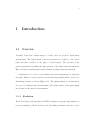
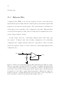
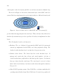
alternating currents or voltages (Figure 1.1). The primary function of a phasemeter
is to provide a high precision measurement of the relative phase of the input signals
in real time for the intended measurement.
1.1.1
Evolution
Before Very Large Scale Integration (VLSI) techniques began appearing, high-speed
processors, high-speed A/D converters, and other high performance electronic devices
2
Figure 1.1: A phase difference ϕ between two alternating input signals: the reference
signal (red) and the measurement signal (blue).
were not available for instrumentation. Phasemeters could only be implemented based
on analog circuitry. One advantage of the analog phasemeter is that there is no loss
of information due to digitization; thus it keeps the continuous nature of the signals.
However, in an analog circuit, some components or features cause artificial phase
shifts, such as oscillators, filters, etc. Devices whose responses are not linear on all
measuring intervals create a more significant problem [1]. Because of these issues,
analog phasemeters can only typically achieve a resolution of approximately 0.5◦ [2;
3].
After the development of high-performance digital devices, it is possible to
implement a digital phasemeter with high resolution, high precision, and high
bandwidth. Currently, there are two main phasemeters widely used in commercial
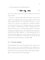
applications, one is a classical stand-alone instrument (Figure 1.2(a)) and the another
is a virtual instrument (Figure 1.2(b)).
The classical stand-alone instruments include common oscilloscopes, function
generators, etc., whose entire functional circuitries are held in cuboid cases. Panel
connectors to detect or transmit signals are typically mounted on the front panel with
a measurement displayed as shown in Figure 1.2(a). This kind of phasemeter is easy
and simple to operate, while its functions are fixed after manufacturing, with little
3
(a) Powertekr Model SD1000 [4]
(b) Zygo ZMITM 4004 [5]
Figure 1.2: The classical stand-alone instrument phasemeter (a) and virtual
instrument phasemeter (b).
modifications or upgrades.
Virtual instruments represent a new method to develop instruments which are
based on the modular measurement hardware. These are usually plug-in boards
(Figure 1.2(b)) with a host PC or specific chassis (for instance, a NI VME Chassis)
with the software running on a host PC to execute their measurements. These results
are then either displayed a monitor, directly transmitted to a controller, or recorded
for post-processing. One of its advantages is that the functions of the instruments
are user-customized to some degree. By modifying and reconfiguring the algorithm
with software, different measurement and data processing can be implemented on the
same hardware. The virtual instruments decrease the volume of the measurement
system, but increase the dependence on computers.
1.1.2
Application
One application area for a phasemeter is with displacement interferometers to measure
displacements with high dynamic range and/or to calibrate other measurement tools.
Two example applications are the Laser Interferometer Space Antenna (LISA) [6] and
4
stage metrology for photolithography [7].
LISA is designed for detecting and studying gravitational waves in a frequency
range between 10−4 and 10−1 Hz [6], which are from sources throughout the universe
such as black holes. When a gravitational wave passes through the plane of the LISA
antenna, it changes the distances between the spacecrafts with a nominal arm length
of 5 × 10⁶ km [8], thus, changes the phase of the interferometric fringe formed at the
LISA interferometers. LISA will measure the phase as a time series signal. From
this time series, the phasemeter can be extrapolated to determine gravitational wave
√
information. LISA is expected to have a strain sensitivity in the order of 10−20 / Hz,
therefore, it should have capability to measure the displacement variation with a
√
sensitivity about 12 pm/ Hz [9].
A photolithography stepper machine is used for the fabrication of semiconductor
chips.
The stepper is usually equipped with a number of heterodyne laser
interferometers to measure and control the motions of the wafer stage, reticle stage,
and other components [7]. The interferometers provide the motion feedback using
frequency modulated interferometry. This is used to support the projection of fine
patterns of integrated circuits onto silicon wafers (Figure 1.3). The semiconductor
device fabrication technology has reached 22 nm in 2012, and it is approaching to
next node at 14 nm [10]. The interferometer and the phasemeter must have improved
resolution, precision, and synchronization to aid in achieving that.
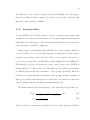
One displacement measuring interferometer (DMI) used in the Precision
Instrumentation Group at the University of Rochester is a custom configuration used
to measure displacement and rotation angle changes with a compact architecture.
Figure 1.4 shows the configuration of the interferometer [12]. In this configuration, the
two photodiodes PDr and PDm measure the reference and measurement interference
5
Figure 1.3: Photolithography stepper machine with interferometers.
interferometers and their phasemeters serve for orientation and control [11].
The
Figure 1.4: The configuration of the displacement measurement interferometer used
in the lab [12].
6
signals, which are
ur (t) = Ur sin (2πfs t) and
(1.1)
um (t) = Um sin (2πfs t + ϕ) ,
(1.2)
where Ur and Um are the amplitudes of the reference and measurement signals, fs
is the nominal split frequency of the laser source, and ϕ is the phase shift, which
contains the displacement of the moving target. The relationship between the phase
difference and the displacement of target is
ϕ=
2πN ∆xηf
.
c
(1.3)
where ϕ is the phase difference between the reference and measurement signals, N
is the interferometer constant (two for this interferometer), η is the refractive index
along the optical path difference, f is the nominal frequency of the laser source, c is
the speed of light, and ∆x is the displacement of the target.
The phasemeter is the measurement instrument used to extract this phase
difference between the reference and measurement signals based on signal processing
algorithms.
There are three mainstream algorithms used to extract the phase
information which are discussed in the following sections.
1.2
Zero-crossing Algorithm
A zero-crossing algorithm focuses on specific points on the reference and measurement
signals within the waveform and measures the delay between these points. The
chosen point is commonly the zero-crossing point within the waveform. The schematic
7
diagram of this algorithm is shown in Figure 1.5 [13].
Ref.
Comp.
XOR
Meas.
Counter
N
Comp.
Clock
Figure 1.5: The schematic diagram of the zero-crossing algorithm.
First, the digitalized reference and measurement signals are fed into comparators.
These two comparators compare the input signals with the zero level. If the signal is
positive, it is converted to a high level (logic “1”) signal, or to a low level signal (logic
“0”) when it is negative. This step realizes zero point detection [13]. Comparators
typically have artificial hysteresis built into the circuit to prevent jitter from creating
false zero crossings [14].
Next, one important step of this method is the “Exclusive OR” (XOR) logic
operation between reference and measurement logic signals [1].
XOR operation
produces a value of “1” only when the truth values of two operands are different.
This step realizes the phase difference extraction, because the pulse duration of
XOR product is equal to the phase difference between the input signals. Figure 1.6
demonstrates this logic operation.
The result of the XOR operation is a series of pulses. Then a counter records the
amount of clock cycles during one pulse [15]. This step realizes the phase difference
measurement. Assuming the amount of clock cycles during one pulse is N and the
amount of clock cycles during one reference signal period is M , the phase difference
8
A
B
A xor B
Figure 1.6: The Exclusive OR operation of two logic signals.
P is
P =
N
× 2π.
M
(1.4)
Therefore, the phase difference can be calculated through the zero-crossing algorithm.
Interpolation can be used to determine fractions of a clock cycle [16].
The limitation of this algorithm essentially comes from the counter clock (sampling
rate). This method needs an ultra-high frequency counter clock when both high
input signal frequency and high phase resolution are required by the phasemeter
simultaneously. The product of the reciprocal of the phase resolution and the input
signal frequency equals the required frequency of the counter clock. For instance, a
digital zero-crossing phasemeter at 1 MHz input and 1/1000 resolution would require
a 1 GHz clock. However, a digital circuit working at those high speeds in practice
must have high-speed signal integrity analysis and a specifically designed PCB. Even
then, it may still have some unpredictable problems. Even if the speed of clock is not a
problem, the precision of its signal edge still may limit the measurement precision [1].
9
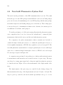
1.3
Phase-locked Loop based Lock-in Detection
Algorithm
Lock-in detection algorithms apply a phase-locked loop (PLL) as the crucial part
of the entire algorithm. Though it relies on a series of complex signal processing
steps, this algorithm can capture the phase difference between two input signals. The
schematic diagram of the algorithm is shown in Figure 1.7 [17].
Ref.
LF
VCO
LPF
VCO
Meas.
ATAN
Unwrap
LPF
Figure 1.7: The schematic diagram of the phase-locked loop algorithm.
The input reference signal ur (t) and measurement signal um (t) are the same as
those shown in Equations 1.1 and 1.2.
First, the reference signal is fed into the PLL. The PLL is a module which is
able to lock the incoming signal’s frequency fs and phase. Two voltage controlled
oscillators (VCO) generate in-phase (I) and quadrature (Q) signals at frequency fs .
One VCO signal is used to feedback into the PLL. More details about principle of the
PLL will be introduced in following section. As Figure 1.7 shows, the PLL generates
10
the in-phase Ir (t) and quadrature Qr (t) signals,
Ir (t) = sin (2πfs t) and
Qr (t) = cos (2πfs t) ,
(1.5)
(1.6)
where the amplitude of the reference signal Ur and measurement signal Um have been
scaled by amplifiers or other digital methods.
Then the measurement signal is separately multiplied by each of two PLL output
signals. Based on the trigonometric product-to-sum identity, the products equal to
a sum of one high-frequency (4πfs ) component and one low-frequency or DC (ϕ)
component. The products are
I(t) = um (t) · Qr (t)
= sin (2πfs t + ϕ) · cos (2πfs t)
=
1
1
sin (4πfs t + ϕ) + sin ϕ, and
2
2
(1.7)
Q(t) = um (t) · Ir (t)
= sin (2πfs t + ϕ) · sin (2πfs t)
1
1
= − cos (4πfs t + ϕ) + cos ϕ.
2
2
(1.8)
Next, the following low-pass filters block these high-frequency components at 4πfs .
The phase difference information from only the DC components is needed, thus the
remaining in-phase I and quadrature Q signals contains phase difference information.
1
sin ϕ, and
2
1
Q = cos ϕ.
2
I=
(1.9)
(1.10)
11
In the end, an inverse tangent operation of Q/I will extract the phase difference
ϕ by
( )
(
)
Q
cos ϕ
ϕ = arctan
= arctan
.
I
sin ϕ
(1.11)
Because of the inverse tangent operation with a principal value in the range
(−π, π], the output signal is wrapped to the interval (−π, π]. Thus, an unwrap
function must follow the inverse tangent operation to make the instantaneous phase
difference continuous.
The following section details the principles of a PLL.
1.3.1
PLL
A phase-locked loop is a crucial part in this algorithm, which is a circuit synchronizing
an output signal with input signal in phase. Frequency is the time derivative of
phase. Locking the input and output phases implies locking frequencies, otherwise,
it is meaningless to compare the phases of two signals with different frequencies. In
“locked” state, the frequency error between the output signal and input signal is zero,
and the phase error remains constant. Hence, it is used to generate the input signal’s
in-phase and quadrature signals in this algorithm.
A PLL consists of three basic functional blocks. Regardless of the type of PLL,
analog or digital, hardware or software, the mechanisms are all the similar. The
structure of PLL is shown in Figure 1.8, which includes a voltage-controlled oscillator
(VCO) or numerically controlled oscillator (NCO), a phase detector (PD), and loop
filter (LF).
To illustrate the principle of the PLL, the following signals must be considered
• The input (reference) signal ui (t),
12
ui(t)
ωi
ud(t)
PD
uo(t)
ωo
LF
VCO
uf(t)
θe
Figure 1.8: The structure of the PLL.
• The angular frequency ωi of the input (reference) signal,
• The output signal uo (t) of the VCO,
• The angular frequency ωo of the output signal,
• The output signal ud (t) of the phase detector,
• The phase error θe , defined as the phase difference between signals ui (t) and
uo (t).
The following section mainly focuses on the expression and derivation of these signals
to describe the functionality of the PLL [18].
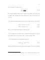
Phase Detector
The Phase Detector (PD) compares the phase of the output signal with the phase
of the input signal and generates an output signal ud (t), which consists of a
low-frequency or DC component and a high-frequency AC component. The AC
component is undesired, hence it is removed by the low-pass loop filter.
The forms of the PD circuit are diverse, including analog and digital variants.
For a basic analysis, the PD with a sinusoidal response characteristic is commonly
used, because of its mature theory and straightforward analysis. Theoretically, an
13
ideal multiplier can be regarded as a PD with a sinusoidal response characteristic.
Therefore, the multiplier is chosen as an example to explain how PD works in a PLL.
In a PLL, the input signal ui (t) is mostly a sine wave and is given by
(
)
ui (t) = Ui sin ωi t + θi (t) ,
(1.12)
where Ui is the amplitude of input signal, ωi is angular frequency and θi (t) is its phase.
The second input signal uo (t) is the VCO output signal and is given by
(
)
uo (t) = Uo cos ωo t + θo (t) ,
(1.13)
where Uo is the amplitude, ωo is the quiescent frequency of the VCO, and θo (t) is its
phase.
The product of these two signals, which is the output of multiplier (PD), is given
by
ud (t) =Km ui (t)uo (t)
(
)
(
)
=Km Ui sin ωi t + θi (t) Uo cos ωo t + θo (t)
(
)
1
= Km Ui Uo sin (ωi + ωo )t + θi (t) + θo (t)
2
(
)
1
+ Km Ui Uo sin (ωi − ωo )t + θi (t) − θo (t) ,
2
(1.14)
where Km represents the gain of the multiplier, whose physical unit is the reciprocal
of voltage, ud consists two terms, one with high-frequency ωi + ωo and one with lowfrequency ωi − ωo or DC level.
Comparing this procedure to phase demodulation, if ωi = ωo , PD extracts the
phase information (phase difference) from the carrier waves (two input signals).
14
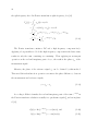
Loop Filter
As discussed above, the output signal of the PD consists of a low-frequency or
DC component and a high-frequency AC component.
approximately proportional to phase difference.
The DC component is
The AC component has high
frequency ωi + ωo , which an unwanted signal. It must be filtered out by a loop filter,
which must pass the lower frequency and block the higher frequency. Hence, it must
be a low-pass filter. In most PLL designs, a first-order low-pass filter is used [18].
The output signal of the PD (Equation (1.14)) is fed into a low-pass filter and the
output signal of the filter1 is
(
)
1
uf (t) = Km Ui Uo sin (ωi − ωo )t + θi (t) − θo (t) .
2
(1.15)
1
Kd = Km Ui Uo ,
2
(1.16)
If
ωe = ωi − ωo , and
(1.17)
θe (t) = θi (t) − θo (t),
(1.18)
where Kd is the phase detection sensitivity in volt per radian, ωe is the frequency
difference between the two PD input signals, and θe (t) is the instantaneous phase
difference between the two PD input signals.
1
The filter has a transfer function F (s). In fact, the low-pass filter does not just pass the lowfrequency components and block the high-frequency components, it also introduces the phase delay
depended on the type of filter. In the PLL, the phase delay influences the phase of the output
signal of the filter uf (t) rather than the output uo (t) of the entire PLL. Hence, for the simplicity,
the following derivations just ignore the phase delay from F (s), and reach the same conclusion.
15
Therefore, uf (t) can be expressed as
(
)
uf (t) = Kd sin ωe t + θe (t) .
(1.19)
which indicates that the PD (with LP) has a sinusoidal response. Figure 1.9 shows
the characteristic of response of the PD (with LP), when ωe = 0. As shown in the
uf(t)
-
0
2
3 θe(t)
Figure 1.9: The characteristic of the response of PD with LP.
figure, uf (t) is approximately linear in a limited interval, where ωe t + θe (t) is very
small. Thus, the sine function can be replaced by its argument around zero:
(
)
uf (t) = Kd ωe t + θe (t) .
(1.20)
Voltage-Controlled Oscillator
In a PLL, a VCO is used for adjusting the frequency through the input voltage. The
VCO oscillates at an angular frequency ω2 , which is determined by input voltage.
The DC level output of a low-pass filter (loop filter) is applied as control signal to the
VCO. The output angular frequency ω2 of the VCO is directly proportional to input
DC level uf (t) and is given by
ω2 = ωo + Ko uf (t),
(1.21)
16
where Ko is called the VCO gain, and its units are radian per second per volt. The
unit radian is often omitted because it is a dimensionless quantity. The quiescent
angular frequency of the PLL is ωo . Figure 1.10 shows an idealized representation of
ω2 as a function of uf (t) of a VCO. It is assumed that the range of the control signal
is symmetrical around uf (t) = 0.
ω2
Ko
ωo
uf(t)
Figure 1.10: An idealized characteristic of a VCO.
In a PLL, the PD, LP, and VCO are implemented in a closed loop with negative
feedback. The mathematical model of PLL is shown in Figure 1.11. In the following
section, the mechanism how to track the input signal’s phase and frequency will be
discussed.
θi(t)
+
θe(t)
-
Kdsin[ ]
vd(t)
F(s)
vf(t)
Ko/s
θo(t)
θo(t)
Figure 1.11: The mathematical model of PLL.
1.3.2
Phase locking Mechanism
First, assuming the frequency of the input (reference) signal ωi is equal to
the quiescent frequency of the VCO ωo 2 , the frequency difference ωe is zero
2
The frequency of the VCO output signal ωo is equal to its quiescent frequency ωv initially.
17
(Equation (1.17)). If the phase difference θe is zero, the output signal of the PD
ud (t) only has a high frequency component (Equation (1.14)). Consequently, the
output signal of the low-pass loop filter uf (t) will also be zero. The output signal is
exact same as input signal, which means the phase has been locked.
Then, if the phase error θe was not zero initially, the PD would develop a nonzero
output signal ud (t), and the LP would also produce a finite signal uf (t). This would
cause the VCO to change its operating frequency in such a way the phase difference
finally vanishes. The phase of the VCO output signal is adjusted until it becomes
equal to the phase of input signal.
Generally, the frequencies of these two input signals of PLL are different initially
and it is meaningless to compare the phases under the condition of different
frequencies. In order to compare these two phases, the instantaneous phase of ui (t)
must be redefined based on the VCO’s quiescent angular frequency ωo ,
[
]
ωi t + θi (t) = ωo t + (ωi − ωo )t + θi (t)
= ωo t + θ1 (t),
(1.22)
where
θ1 (t) = (ωi − ωo )t + θi (t)
= ωe t + θi (t).
(1.23)
The instantaneous phase, θ1 (t), is based on VCO’s output frequency as a reference.
Then, the VCO output signal is rewritten by replacing θo (t) with θ2 (t), and is
given by
ωo t + θo (t) = ωo t + θ2 (t).
(1.24)
18
The following is a mathematical approach to describe the whole mechanism.
Phase is the time integral of frequency, thus, integrating both sides of
Equation (1.21) yields
∫
∫
t
ω2 (t)dt = ωo t + Ko
0
t
uf (t)dt.
(1.25)
0
Therefore, according to Equation (1.13), the instantaneous phase θ2 (t) of uo (t) when
the reference frequency is ωo , is given by
∫
θ2 (t) = Ko
t
uf (t)dt.
(1.26)
0
Here, for simplicity, assume that the difference between the angular frequency of
the input signal and the quiescent angular frequency of the VCO ωe is constant as
well as the phase of input signal θi .
Inserting these substitutions from Equation (1.18) and Equation (1.20) into
Equation (1.26), results in the phase output, given by
∫
t
θ2 (t) = Ko
uf (t)dt
∫
0
t
Kd (ωe t + θe (t))dt
= Ko
∫
0
= Ko
t
(1.27)
(
)
Kd θ1 (t) − θ2 (t) dt.
0
Assuming K = Ko Kd , and the Laplacian is taken of both sides,
(
)
K Θ1 (s) − Θ2 (s)
.
Θ2 (s) =
s
(1.28)
19
The transfer function H(s)3 is given by
H(s) =
Θ2 (s)
K
=
.
Θ1 (s)
K +s
(1.29)
In the time domain, the transfer function is given by
h(t) = Ke−Kt u(t).
(1.30)
The phase of output signal is a convolution of the phase of the input signal and the
transfer function. Inserting these substitutions (Equation (1.23) and Equation (1.30)),
the instantaneous phase of the output signal is given by
∫
t
θ1 (τ )h(t − τ )dτ
θo (t) = θ2 (t) =
∫
0
)
ωe τ + θi (τ ) Ke−K(t−τ ) dτ
0
)
(
(
)
e−Kt
1
= ωe t −
+
+ 1 − e−Kt θi (t).
K
K
=
t
(
(1.31)
When time t is sufficiently long,
lim θ2 (t) = ωe t + θi (t) = θ1 (t),
t→∞
(1.32)
the instantaneous phase of the output signal approaches to that of the input signal.
This duration is not necessary very long and depends on a proper factor K.
After θ2 approaches to θ1 , the state is so-called “phase-locked”. Because the
3
For the simplicity, it ignores the transfer function F (s) of the loop filter, but the trend of θ2 (s)
approaching to θ1 (s) is not changed.
20
output signal is assumed initially as
(
)
uo (t) = Uo cos ωo t + θo (t)
(1.33)
when the phase is locked, the actual output signal is the quadrature signal of the input
signal. That is the crucial mechanism of PLL to generate the quadrature signal.
To generate the in-phase signal of the input signal, it can simply set the initial
phase of Equation (1.33) to advance or delay 90◦ . The rest mechanism is identical
with that of quadrature signal.
1.4
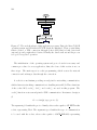
Single-bin DFT Algorithm
A single-bin discrete Fourier transform (SBDFT) has been used in the LISA
phasemeter [19; 20], which uses the phase of certain bin in the Fourier spectrum
to trace the phase change of the input reference and measurement signals.
According to Fourier theory, for a sinusoidal signal, the energy in the frequency
spectrum is concentrated at the nominal signal frequency. The phase of the signal at
a specific time is the phase of the Fourier transform at the point where the energy is
concentrated. The phase measurement can be implemented by comparing the phase
of the reference signal and phase of the measurement signal at any time [21].
The phasemeter only focuses on a point at or a limited range around nominal
frequency of the signal rather than the entire frequency spectrum. Thus, it can
calculate the Fourier transform only in that range. That range is constrained by a
single bin. Frequency bins are even intervals spaced by frequency lines in the discrete
Fourier Transform (DFT) spectrum, which can be computed by the sampling rate
21
fsample and number of samples Nsample ,
bin =
fsample
.
Nsample
(1.34)
For example, assuming 10,000 points are sampled at 100 MHz, each frequency bin
is 10 kHz. Only calculating the Fourier transform in a single bin saves time and
resources.
The input measurement signal um (t) and reference signal ur (t) are of the forms
um (t) = cos (2πfs t + ϕm ) , and
ur (t) = cos (2πfs t + ϕr ) ,
(1.35)
(1.36)
where fs is the nominal split frequency of the laser source.
For the simplicity, the following uses a continuous Fourier transform to express
the algorithm. However, it reaches the same conclusion as using a DFT.
The Fourier transform of the measurement signal is
∫
Um (f ) =
∞
−∞
um (t)e−i2πf t dt.
(1.37)
Because only the Fourier transform at the nominal frequency4 is needed, specifically,
4
It can be regard equivalent to the bin, which covers the nominal frequency in DFT spectrum.
22
the split frequency here. Its Fourier transform at split frequency fs is [22]
∫
Um (fs ) =
∞
∫−∞
∞
=
−∞
um (t)e−i2πfs t dt
cos (2πfs t + ϕm ) e−i2πfs t dt
∫
1 ∞ i(2πfs t+ϕm )
=
(e
+ e−i(2πfs t+ϕm ) ) · e−i2πfs t dt
2 −∞
∫
1 iϕm 1 ∞ −i(4πfs t+ϕm )
= e +
e
dt.
2
2 −∞
(1.38)
The Fourier transform contains a DC and a high frequency component 4πfs .
Applying a low-pass filter to block the high frequency component in the latter term,
results in only the term containing ϕm remaining. Then applying an arctangent
operation on the real and imaginary parts of eiϕm , the result is the phase ϕm of the
measurement signal.
Likewise, the phase of the reference signal ϕr can be obtained by this method.
Then an additional subtraction operation can extract the phase difference ϕ between
the measurement and reference signals,
ϕ = ϕm − ϕr .
(1.39)
According to Euler’s formula, the real and imaginary parts of the term e−i2πfs t in
the Fourier transform calculation actually is a quadrature signal Qs and an in-phase
Is [23],
Qs (t) = Re{e−i2πfs t } = cos (2πfs t) , and
(1.40)
Is (t) = Im{e−i2πfs t } = − sin (2πfs t) .
(1.41)
23
Hence, the single-bin DFT algorithm is 2-channel lock-in detection algorithm
essentially, but without a PLL. It replaces the PLL with the in-phase Is and
quadrature Qs signals, and treats them as in-phase and quadrature signals of the
reference signal in the PLL algorithm. It treats the measurement and reference
signals both as the measurement signals in PLL algorithm (Equation (1.7) to
Equation (1.11)). Unlike the PLL algorithm which calculates the phase difference
directly, the single-bin DFT algorithm first compares the phases of the measurement
and reference signals with a signal with the split frequency to calculate the phase
differences separately, then performs a subtraction operation to obtain the difference
between these two phase differences, which is the relative phase difference between
measurement and reference signals. Figure 1.12 shows the schematic diagram of the
algorithm.
Ref.
LPF
ATAN
Unwrap
VCO
LPF
_
VCO
LPF
+
ATAN
Meas.
Unwrap
LPF
Figure 1.12: The schematic diagram of the phase-locked loop algorithm.
24
1.5
Motivation and Goals
The phase measurement solution currently used in the Precision Instrumentation
Group Lab includes a commercial single element photodetector, a commercial
quadrant photodetector, lock-in amplifiers, a NI PCI or USB data acquisition card,
and a target PC. Some of them have limited performances or shortcomings, which
will attempt to be improved and addressed in this work.
1. The commercial single element and quadrant photodetectors are used for
detecting the reference and measurement signals respectively. They convert
these interference signals to electrical signals for post-processing.
The
commercial quadrant photodetector currently used has four silicon photodiodes,
each with 2.5 mm side square pixels in a 2×2 arrangement. For differential
wavefront sensing, this area can only provide a limited spatial sensitivity [24].
Additionally, the performance of this system is less than adequate with op-amp
oscillations and a lack of decoupling capacitors.
2. The lock-in amplifiers are used to extract the phase difference between reference
and measurement signals. The lock-in amplifiers currently used are model SRS
SR830 from Stanford Research Systems. It has a limited bandwidth 1 mHz to
102.4 kHz, which is sufficient for locking 70 kHz split frequency signal, but is
not suited for higher split frequency 5 MHz. Also, it is an instrument with large
dimensions (17′′ W×5.25′′ H×19.5′′ D), heavy weight (23 lbs), significant power
consuming (40 W) [25], and high price (about $5000). In practice, the consumed
power converts into heat partly, the fan inside the chassis generates noise and
vibration, which may cause problem for ultra-precision application. When
25
stacking four these instruments for processing differential wavefront sensing
signals, there is the potential for synchronization issues.
3. The transmission interface is used to exchange the measurement data between
measurement instrument and computer for post-processing, analysis, control.
The transmission solution currently used is a NI PCI data acquisition card,
which acquires the lock-in amplifier’s analog output signal first, and then
transmits the measurement data to computer through PCI interface. This
solution costs an extra $1000 to employ this extra hardware to convert the
analog signal to digital signal and transmit it, which may be replaced by readily
available hardware in computer, if measurement instrument outputs digital
signal directly. Other virtual instrument type phasemeters usually equip with
an instrument specific interface, such as the Zygo ZMI 4004 phasemeter with
a VME interface, which are not equipped in common computers. This type of
phasemeter must collaborate with specific chassis with these interface slots. The
chassis generally costs thousands of dollars. It usually has several slots, while
only one is needed for this particular application, others are spare. Hence, these
data transmission solutions are not economical, user-friendly, or/and easily
accessible.
4. The entire phase measurement solution currently used now is large-volume,
dispersed, complicated-operation, and expensive as a system.
The goal of this work is to improve those shortcomings to some degree, and
design a high-speed, high-precision, compact, economical and user-friendly interface
phasemeter prototype to measure, process, and transmit data.
1. To achieve high spatial sensitivity for differential wavefront sensing, a large
26
active area quadrant photodiode will be used for building the measurement
photodetector. To achieve a low noise level output signal, a specific analog
signal processing board will be designed for the photodetector. In the initial
prototype, the photodiode will work in photovoltaic mode for sensing 70 kHz
signal. The processing board will be able to adjust the output signal voltage for
the incident optical power 1 µW to 50 µW, maintain the output voltage as 1 to
2 Vp-p . Chapter 2 will discuss the photodetector and analog signal processing
board design, device selection, printed circuit board design, and the simulation
and verification below in detail.
2. A FPGA board will implement the PLL and SBDFT algorithm to extract the
phase difference. As the digital signal processing module of the phasemeter
system, it will be high-precision (sub-nanometer), high-speed (50 MSPS), widebandwidth (5 MHz), small-volume, silent, user-customized, and economical. It
is sufficient to replace the lock-in amplifier. In the initial prototype, due to the
limited resource on the FPGA chip used now, only one channel measurement
signal will be processed. Chapter 3 will introduce the hardware and software
used to implement the algorithm, discuss the fixed-point models design, and
simulation and verification below in detail.
3. This phasemeter system will use an Ethernet interface to transmit measurement
data between FPGA board and computer through UDP packets.
The
transmitter will be implemented by a soft-core processor in the FPGA, the
receiving end will be implemented in a target PC. An Ethernet cable connects
the Ethernet port on FPGA board with the Ethernet adapter card in the target
PC. There will be no extra hardware used in this system. It is economical,
user-friendly, and easy-access. Chapter 4 will introduce the mechanism of UDP,
27
discuss the transmitter and receiving end implementations, and the test results.
28
29
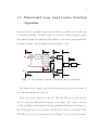
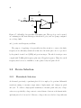
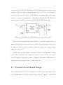
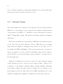
2
Detection and Processing
Board Design
Before calculating the phase difference between reference and measurement signals,
the optical signals must be converted into electrical signals for further electrical
circuitry to process initially. Additionally, some filters and amplifiers circuits are
required to keep the converted electrical signals in good quality, because stray light
in environment mixed in the laser beams may also be converted, and the optical
devices in previous configuration and the electronic components on-board introduce
noise inherently. Thus, a detection and analog signal processing circuit must be built
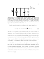
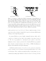
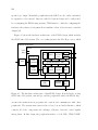
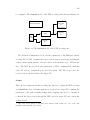
in this design firstly. Figure 2.1 shows the diagram of this circuitry.
This work only designed the circuitry for the measurement beam. Following
sections will discuss the principle of this circuitry, devices selection, and printed circuit
board design in detail.
30
TIA
HPF
IA
LPF
ADC
TIA×4
HPF×4
IA×4
LPF×4
ADC×4
Analog
Figure 2.1: The diagram of the detection and processing circuitry. The reference
and measurement beams incident one signal-element and one quadrant photodiode
respectively, and then are converted to weak electrical current signals. And
the following processing circuits are based on operation amplifiers, which are
transimpedance amplifiers (TIA), high-pass filters (HPF), inverting amplifiers (IA),
and low-pass filters (LPF). Finally, the signals will be fed into ADCs to convert to
digital signals for further computation (the ADCs are on a separate board in this
design). This work mainly designs the circuitry for measurement signals channels.
2.1
2.1.1
Detection and Processing Principles
Photodiodes
Silicon photodiodes are semiconductor devices with p-n junctions or PIN structures.
They operate by absorbing photons or charged particles and generating photocurrent
in an external circuit, which is proportional to the incident optical power. This
mechanism is also known as the inner photoelectric effect [26].
A silicon photodiode can be represented by an ideal diode in parallel with a
current source and some resistors and a capacitor. The current source generates the
photocurrent corresponding to the incident optical power and the diode represents
the p-n junction or PIN structure. In addition, a junction capacitor and a shunt
resistor are parallel to the current source and ideal diode. A series resistor and all
other components in this model are in a series connection. An equivalent circuit of a
photodiode is shown in Figure 2.2 [27; 28].
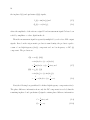
31
Rs
Iout
Id
Iph
PD
Cj
Rsh
I′
Figure 2.2: Photodiode equivalent circuit. Iph is the generated photocurrent; Id is
the dark current; I ′ is the shunt resistor current; Iout is the output current; Cj is
the junction capacitor, where the value depends on the applied reverse bias voltage
and determines the response bandwidth of the photodiode; Rsh is the shunt resistor,
its actual value ranges from 10’s to 1000’s of megaohms; Rs is the series resistor, its
typical value ranges from 10 to 1000’s ohms.
Using the equivalent circuit shown in Figure 2.2, the output current Iout is
( eVd
)
Iout = Iph − Id − I ′ = Rλ P − Is e kT − 1 − I ′ ,
(2.1)
where Rλ is the responsivity or photosensitivity of the photodiode, measuring the
effectiveness of the conversion of optical power into photocurrent, expressed in A/W.
Its value depends on the wavelength of the incident light, applied reverse bias voltage,
and temperature. Also, P is the incident optical power, Vd is the applied reverse bias
voltage across the diode, Is is the photodiode reverse saturation current, e is the
electron charge, k is Boltzmann’s constant, and T is the absolute temperature.
A photodiode can be operated in two modes: photoconductive (reverse bias) or
photovoltaic (zero bias). The mode selection depends on the application’s response
speed and sensitivity requirements.
Photoconductive mode achieves the fastest
response and greatest bandwidth, while introducing dark and noise current that harm
the photodiode sensitivity. Photovoltaic mode achieves the highest sensitivity but has
a slower response [29].
32
In this design, photovoltaic mode was selected because the photodiode is used in a
low frequency regime (up to 200 kHz) and a precision application. The photocurrents
in this mode have less variation in responsivity with temperature, no dark current
is generated by this mode, and the shunt resistor current is negligible.
Thus,
Equation (2.1) simplifies to
Iout = Rλ P.
(2.2)
The photodiode can operate in zero bias to eliminate any additional noise current to
achieve a high sensitivity.
Photodiodes can be used for more than sensing the presence or absence of light
at certain wavelengths; they also can be used to quantify light intensities below
1 pW/cm2 to intensities above 100 mW/cm2 for extremely accurate measurements.
In this design, a quadrant photodiode is used to perform differential wavefront
sensing, measuring the target mirror displacement, pitch, and yawthrough measuring
four spatially separated interference signals on the four elements of the quadrant
photodiode [24; 30; 31]. Silicon photodiodes can also be utilized in other diverse
applications such as spectroscopy, photography, analytical instrumentation, optical
position sensors, beam alignment, surface characterization, laser range finders, optical
communications, and medical imaging instruments [28].
2.1.2
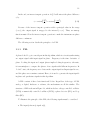
Transimpedance Amplifier
A transimpedance amplifier is an amplifier circuit that generates an output voltage
proportional to the input current.
The proportionality of this conversion is
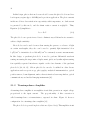
called transimpedance or transresistance, expressed in ohms. Figure 2.3 shows a
configuration for a transimpedance amplifier [32].
The photodiode is operated in photovoltaic mode (zero bias). This amplifier circuit
33
Cf
Rf
Ip
−
Vout
+
C′
R′
Figure 2.3: Configuration for a photovoltaic transimpedance amplifier.
provides approximate zero input impedance Rf /A, because of the operation amplifier
(op-amp) properties: virtual ground and very high open loop gain A. Compared with
the output resistance of photodiodes, the input resistance of the amplifier circuit
is negligible, despite Rf is generally very large. This results in no voltage drawn
down across the diode and then no diode leakage current basically. The temperature
coefficient of the amplifier input leads to a thermal DC voltage drift, an equal
resistance R′ connected in series with op-amp noninverting input could compensate it,
and a bypass capacitor C ′ could remove most of its noise. However, this may create a
voltage drop across the diode and results in diode leakage current [33]. Additionally,
in order to suppresses potential oscillation or gain peaking, a small capacitor Cf is
placed across Rf to act as a low-pass filter cooperating with Rf . This can affect the
bandwidth of the system [29].
The relationship between input current and output voltage is given by
Vout = −Rf Iin .
(2.3)
34
In this design, the input current is microamps and the output voltage is several volts.
The values for Rf and Cf must be carefully selected to achieve enough gain and
bandwidth.
Transimpedance amplifiers are usually used in optical communications receivers
or after photodetectors to convert the photocurrent into a voltage signal for further
manipulation. The motivation to implement transimpedance amplifiers is that a
voltage signal is generally easier to process than microamps of photocurrent signal
for following stages.
2.1.3
Buffer Amplifier
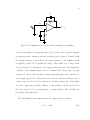
A buffer amplifier (sometimes simply called a buffer) is a circuit that provides
electrical impedance isolation or matching between previous and following stage
circuits. Two main types of buffers exist: the voltage buffer and the current buffer.
This design employs voltage buffers.
The circuit schematic of a buffer amplifier is shown in Figure 2.4.
Vin
In this
+
Vout
−
Figure 2.4: Schematic of a buffer amplifier. Its output connects to its inverting
input, and the output of previous stage connects to its non-inverting input. This
constructs a full series negative feedback to the op-amp, implementing a unity gain
buffer amplifier.
configuration, the output voltage is connected in series with the input voltage.
According to Kirchhoff’s voltage law (KVL) and properties of an op-amp, the
difference of the two voltages, Vin (V+ ) and Vout (V− ) is proportional to the op-amp
35
differential input based on its open loop gain A. Amplifying A times to Vout , the
relationship between Vout and Vin is [34]
A
Vin ,
1+A
(2.4)
where A is the open-loop gain of the op-amp.
Because A is very large, Vout
Vout =
is approximately Vin . Thus, the closed-loop gain is unity (0 dB). Although the
voltage gain of a voltage buffer amplifier is approximately unity, it usually provides
considerable current gain and thus power gain.
In the Figure 2.4, it is the operation amplifier, an active device, whose properties
determine the buffer function. According to the voltage divider rule, the input
impedance of the op-amp is very high (1 MΩ to 10 TΩ), which means that the
input of the op-amp draws only minimal current from voltage source, thus it does
not load the voltage source (does not influence output voltage of source). The output
impedance of the op-amp is very low, which means it drives the load as if it were a
perfect voltage source (any load does not influence its output voltage). Therefore, the
output impedance of the previous stage and the input impedance of following stage
do not affect each other due to the buffer. This phenomenon is so-called impedance
isolation or impedance matching.
The purpose of placing a buffer at the end of circuit is to avoid the influence from
unknown following circuits. In other words, performing a measurement or processing
a voltage does not disturb the circuit producing the voltage to be measured or
processed. The output signal may propagate through a cable to other analog circuits
or instruments, which are variable, the input impedance of those following stages are
variable as well. A buffer helps to maintain or even promote the performance of the
detection and processing circuitry, especially the drive capability, regardless of the
36
following stage.
2.1.4
High-pass Filter
A high-pass filter (HPF) is an electronic frequency selective circuit that passes
signals with frequencies higher than the cutoff frequency but attenuates signals with
frequencies lower than the cutoff frequency. The actual amount of attenuation for
each frequency varies depending on the configuration of the filter. High-pass filters
are widely used in signal processing, such as blocking DC level signals from non-zero
average voltages sensitive circuitry.
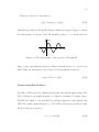
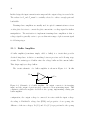
In this design, first-order, noninverting high-pass filters with unity gain
were applied.
Compared with other inverting configurations, the noninverting
configuration has a simpler structure with fewer components to achieve the unity
gain in the passband. Figure 2.5 shows a first-order, noninverting high-pass filter
configuration [35].
C
Vin
+
Vout
−
R
Figure 2.5: First-order noninverting high-pass filter with unity gain. With an op-amp,
this is an active first-order high-pass filter. It consists of a highpass RC network and
a voltage buffer. The buffer serves to provide impedance isolation so the RC network
is not loaded down by the following stages and the output voltage of the RC network
is transferred to the buffer’s output without attenuation. Without the buffer, the
frequency response of a simple RC network on its own would be varied depending on
the load resistance, which is in parallel with the shunt resistor R.
37
The circuit transfer function of this high-pass filter is
H(s) =
Vout (s)
s
s
=
,
1 =
Vin (s)
s + 2πfc
s + RC
(2.5)
where R is the resistance in ohms, C is the capacitance in Farads and fc is the cut-off
frequency in Hertz.
The purpose of employing a high-pass filter in this design is to remove the DC
component. Since input optical power varies and the output of the whole analog
signal processing circuit must be fed into an ADC with a fixed range of 1-2 Vp-p [36],
removing the DC component is more straightforward for adjusting the amplitude
of the signal in the following stage.
Both high-pass filters and low-pass filters
have the capability to adjust the signal gain. However, the high-pass filter has the
limitation that the gain cannot be lower than unity (specifically in the noninverting
configuration) and changing the gain in a wide range influences the cutoff frequency
(specifically in the inverting configuration). So a unity gain high-pass filter and an
independent inverting amplifier are used in the current and following stages. The
cutoff frequency of the high-pass filter is 1 kHz, which removes the DC component
effectively and passes the desired frequency of nominally 70 kHz.
2.1.5
Inverting Amplifier
An inverting amplifier scales and inverts the input signal. If the op-amp open-loop
gain is very large, the closed-loop gain of this amplifier circuit is determined by two
stable external resistors (the feedback resistor Rf and the input resistor Rin ) and is
largely independent from op-amp parameters which are highly temperature sensitive.
Figure 2.6 shows the schematic of the inverting amplifier.
38
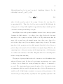
Rf
Rin
Vin
−
Vout
+
Figure 2.6: Schematic of inverting amplifier. The value for Rin in this design is given
by a potentiometer, makes the voltage gain of circuit adjustable.
The noninverting input of the inverting amplifier circuit is grounded. According
to the two assumptions of op-amp properties, virtual short and virtual open, the
feedback keeps the inverting input of the op-amp at a virtual ground (noninverting
input and inverting input are virtual short), and no current flows in the input leads
(noninverting input and inverting input are virtual open). Hence the current flowing
through Rin is assumed to equal the current flowing through Rf . Based on Kirchhoff’s
law, the voltage gain is
G=−
Rf
Rin
(2.6)
and the minus sign here is inserted because this configuration opposes the polarity of
the input signal [37].
The purpose of using an inverting amplifier is scaling the amplitude of the output
signal. This reason was introduced in high-pass filter section. In order to adjust the
gain of the circuit, the value of Rf or Rin must be adjustable as well. If a potentiometer
(used as a variable resistor) is used to drive Rf , the gain linearly correlates the
resistance of potentiometer, which could not be very high. That means the range
of the gain could not be very wide. Using a potentiometer at Rin , the upper limit
of gain is determined by the reciprocal of the minimum potentiometer resistance.
Therefore, the range of gain can be very wide. Meanwhile, the adjustment process is
39
more efficient, because of the inversely proportional relationship. Since the input to
this stage is buffered and the output is processed in an active filter, the issues with
impedance change should be minimal.
2.1.6
Low-pass Filter
A low-pass filter is an electronic frequency selective circuit that passes signals with
frequencies lower than the cutoff frequency but attenuates signals with frequencies
higher than the cutoff frequency. The actual amount of attenuation for each frequency
varies depending on the filter configuration.
In this design, a low-pass filter with a Sallen-Key topology was applied, which is a
second-order filter. A second-order filter has narrower transition band and a steeper
frequency response than a first-order filter. There are two typical topologies for a
second-order low-pass filter: the Sallen-Key and the multiple feedback (MFB) [37].
The Sallen-Key topology, also known as a voltage control, voltage source (VCVS), is
shown in Figure 2.7. The reason of choosing this topology is that its performance
is relatively independent from performance of the op-amp, specifically, which has
relatively loose gain-bandwidth requirements of the op-amp. Another advantage of
this topology is that component spread is low (the ratio between the two resistor and
capacitor values), which is beneficial for manufacturability [38].
The transfer function and cutoff frequency of the Sallen-Key low pass filter are
1
; and
1 + C2 (R1 + R2 )s + R1 R2 C1 C2 s2
1
fc = √
,
2π R1 R2 C1 C2
H(s) =
(2.7)
(2.8)
where R1 and R2 are the resistance in ohms, C1 and C2 are the capacitance in Farads
40
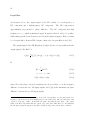
C1
R1
R2
Vin
+
Vout
−
C2
Figure 2.7: Sallen-Key low-pass filter with unity gain. This topology can be treated
as containing two RC networks stages, which have 2 poles, and an op-amp configured
as a voltage buffer.
and fc is the cutoff frequency in Hertz.
The purpose of applying a low-pass filter in this circuit is to remove the highfrequency noise efficiently, whether it is introduced from the photodiode or produced
by the printed circuit board (PCB) and previous stages. The whole circuit processes
a signal with 70 kHz spilt frequency plus varied Doppler frequency. Thus, the cutoff
frequency has been set to 200 kHz to reduce phase delay and gain roll-off.
2.2
2.2.1
Device Selection
Photodiode Selection
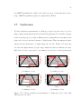
As discussed previously, a quadrant photodiode is employed to perform differential
wavefront sensing to measure target mirror displacement, and changes in pitch
and yaw. To achieve a high spatial sensitivity to measure pitch and yaw, a large
active area, specifically, a large center-to-center distance between each element in the
quadrant photodiode is needed. However, a large active area leads to large inherent
41
capacitance, which narrows the response bandwidth of the photodiode. Thus, these
are tradeoffs that must be balanced when selecting the photodiode.
In this work, the Hamamatsu S5981 was selected for this design. It is a Si
PIN multi-element photodiode for surface mounting.
It has larger active area
than other similar photodiodes, which is a 100 mm2 square including four elements
(quadrants), and has a 20 MHz bandwidth when operated with a 10 V reverse bias.
Its photosensitivity is 0.43 A/W at the wavelength of a red HeNe laser at 633 nm [39].
The photodiode in this design senses a 70 kHz signal with a varied Doppler
frequency at a wavelength of 633 nm, and the optical power of it varies from 1 to
50 µW. The photodiode is configured in photovoltaic mode to achieve high sensitivity
but a narrow bandwidth. From the datasheet, it has 20 MHz bandwidth but only
with a 10 V reverse bias. It still must be tested whether it has at least a 200 kHz
bandwidth with a zero bias. Theoretically, it generates 0.43 to 21.5 µA photocurrent,
depending on the incident optical power.
2.2.2
Op-amp Selection
It is important to choose op-amps that can provide the necessary DC precision, gain,
speed, distortion, and noise. The principles introduced in the previous section assume
ideal op-amps are used, which have following properties:
• Infinite open-loop gain
• Infinite voltage range available at the output
• Infinite bandwidth with zero phase shift
• Infinite slew rate
42
• Infinite input impedance
• Zero output impedance
• Zero input bias and offset current
• Zero input bias and offset voltage
• Zero noise, etc. . . .
None of these ideal properties can exist perfectly in a real op-amp. In a real op-amp,
these properties should be non-infinite or non-zero, which could be modeled with
equivalent resistors, capacitors, voltage sources, and current sources in the op-amp
model. Some parameters may eventually have negligible effect on the final design
while others limit the final performance of the design that must be evaluated. The
following parameters must be carefully considered in this design.
Gain-bandwidth Product
The gain-bandwidth product (GBW or GBP) for an op-amp is the product of the
amplifier circuit’s bandwidth and the closed-loop gain at the bandwidth.
This
parameter is not infinite but fixed in a real op-amp, and it determines the maximum
bandwidth that can be extracted from the amplifier circuit for a given gain and vice
versa. Thus, op-amp applications must balance the tradeoff between two important
parameters gain and bandwidth.
For proper filter functionality, gain-bandwidth product is an important op-amp
parameter. In general, the open-loop gain (AOL ) should be 100 times (40 dB) above
the maximum closed-loop gain (APEAK ) of a filter section to allow a maximum gain
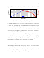
error of 1%, as Figure 2.8 shows.
43
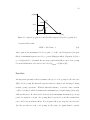
|A| [dB]
AOL
40 dB
APEAK
ACL
A0
fc
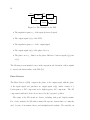
f [Hz]
Figure 2.8: Open-loop gain AOL and the filter response (closed-loop gain) ACL .
A general rule is that
GBW = 100 · Gain · fc
(2.9)
where gain is the maximum closed-loop gain, fc is the cut-off frequency (low-pass
filter) or maximum frequency needed to operate (high-pass filter). Equation (2.9) is a
good design guide to determine the necessary gain-bandwidth product of an op-amp
for an individual first-order and second-order (APEAK < 1) filter [40].
Slew Rate
An important parameter that determines the speed of an op-amp is the slew rate
(SR). A real op-amp has internal capacitors that are charged and discharged during
normal op-amp operations. With its internal resistance, a non-zero time constant
could be calculated, which determines the maximum rate of signal change (slew rate)
without distortion. In other words, slew rate is the maximum transient slope at any
point of a signal in a circuit. An op-amp that is operated beyond the nominal slew
rate could create non-linear effects. For adequate full power response, the slew rate
(in volts per microsecond) of an op-amp at all points of a signal must be greater
44
than [40]
SR = π · Vp-p · fc ,
(2.10)
where Vp-p is the signal peek-to-peek voltage and fc is the cut-off frequency (low-pass
filter) or maximum frequency needed to operate (high-pass filter).
Input Offset Voltage
The input offset voltage parameter, a DC characteristic, is defined as the DC offset
voltage that must be applied between the two input terminals to keep output DC
voltage zero within the op-amp. It is expressed in units of volts.
Due to the manufacturing process, the transistors of the two input terminals in
real op-amps may not be exactly matched, thus zero differential input produces a nonzero output. In order to cancel that output offset, all op-amps require a small voltage
difference between their inverting and noninverting inputs to balance the mismatch.
The required voltage, known as the input offset voltage, VIO , is normally modeled as
a voltage source driving the noninverting input [37].
Input offset voltage is always multiplied by the noninverting gain of the amplifier
circuit and added to (or subtracted from) the signal gain of the circuit. In large-gain
DC-coupled circuits, VIO may be significant and may need to be reduced through
offset adjustment techniques, if the DC accuracy is important [41].
Input Bias Current
Bias current is required by the input circuit of all op-amps for proper operation. The
input bias current IIB , a DC characteristic, is computed as the average of the two
input bias currents I+ and I− .
45
Bias current is a problem for op-amps because it flows in external impedances and
produces voltages. In transimpedance amplifiers, the input bias current generates an
additional output offset voltage with the large feedback resistor. This output offset
voltage may send the output signal into saturation, depending on the op-amp power
supply operation [42]. The best solution is to use an op-amp with either a CMOS or
JFET input due to its very low input bias current [37].
Other
Some op-amps are unity-gain stable, suitable for voltage buffers, while some other opamps are optimized for higher closed-loop gains. Using those non-unity gain stabile
op-amps in buffer applications will cause problems.
The voltage supply range should be wide to leave enough margins for the
amplitude of the output signals of amplifier applications.
This aims to avoid
saturation of output signals.
This circuit processes quadrant photodiode signals, which needs four parallel
channels. It is better to utilize 4-channel chips (four op-amps in single chip) to
implement every stage, which uses the least number of chips and keep the performance
of every channel similar. By selecting each op-amp at each stage, the op-amp can be
tailored to the specific application at that stage.
Devices
The TI OPA4140, OPA4228, and OPA4227 are selected for the transimpedance
amplifiers, filters, and buffer amplifiers, inverting amplifiers, respectively.
The OPA4140 is a high-precision, low-noise, rail-to-rail output, 4-channle, JFET
op-amp. It has [43]:
46
• 11 MHz Gain Bandwidth Product
• 20 V/µs Slew Rate
• 30 µV Input Offset Voltage
• ±0.5 pA Input Bias Current
• ±2.25 V to ±18 V Voltage Supply Range etc . . .
It is suitable for the transimpedance amplifier in this design. This circuit is expected
to process a 70 kHz split frequency plus varied Doppler frequency signal, whose
frequency must be less than 200 kHz. Thus, the cut-off frequency fc of the filter,
consisting of feedback resistor Rf and feedback capacitor Cf (Figure 2.3), is set at
200 kHz. Thus, Rf and Cf are chosen to be 100 kΩ and 8 pF, respectively, which
will be discussed in the following section. From terminal capacitance versus reverse
voltage diagram in the S5981 photodiode, when the reverse voltage is 0.1 V, the
terminal capacitance Cp is 140 pF. This assumes that in zero-bias, the photodiode
has the same 140 pF Cp . A general guide (different from Equation (2.9)) to determine
the minimum GBW requirement for the transimpedance amplifier is [44]
GBW = 2π · fc 2 · Rf · (Cf + Cp )
(2.11)
= 2π · (200 kHz)2 · 100 kΩ · (8 pF + 140 pF)
= 3.7 MHz.
The OPA4140 has an 11 MHz GBW, which is higher than the required 3.7 MHz and
is sufficient for the transimpedance amplifier in this design.
The current from the photodiode is 0.43 to 21.5 µW and produces 0.043 to
2.15 V flowing through the 100 kΩ feedback resistor. The slew rate (according
47
to Equation (2.10)) for this transimpedance amplifier must be greater than
SR = π · 2.25 V · 200 kHz = 1.4 V/µs.
(2.12)
The OPA4140 has a 20 V/µs slew rate, which is much greater than 1.4 V/µs. This
amplifier meets the slew rate requirement.
Considering the transimpedance amplifier has a current input configuration, the
input bias current and input current noise will impact the quality of the output
signal. The OPA4140 has a low input bias current (±0.5 pA), so this impact is low.
The other following stages provides strategies to eliminate this impact, for example,
the following high-pass filter removes the DC offset voltage produced by input bias
current flowing through feedback resistor.
The OPA4228 is a high-precision, low-noise, wide-bandwidth, high-speed 4channel op-amp. It has [45]:
• 33 MHz Gain Bandwidth Product
• 11 V/µs Slew Rate
• 10 µV Input Offset Voltage
• ±2.5 pA Input Bias Current
• ±5 V to ±18 V Voltage Supply Range etc . . .
It is suitable for the active filters in this design. There are one first-order, high-pass
filter and one second-order, Sallen-Key low-pass filter in this design. Based on their
design and applying Equation (2.9), the necessary gain-band product of this op-amp
meets this specification. Both filters have a unity-gain, and their cut-off frequency
48
(low-pass filter) or maximum operating frequency (high-pass filter) is 200 kHz. Thus,
for filters, the GBW of the op-amps should at least be
GBW = 100 · 1 · 200 kHz = 20 MHz.
(2.13)
The OPA4228 has a 33 MHz GBW, which is higher than the 20 MHz required and
enough for the active filters in this design.
The high-pass filter just blocks the DC voltage and the peak-to-peak voltage of
its AC signal is almost same as that of the transimpedance amplifier. The gain of
high-pass filter is unity. So the minimum slew rate of the op-amp for the high-pass
filter is 1.4 V/µs.
The inverting amplifier before the low-pass filter adjusts the amplitude of signal
to match the amplitude of input signal of the ADC, which is at most 2 Vp-p . The
minimum slew rate of the low-pass filter needed is
SR = π · 2 V · 200 kHz = 1.26 V/µs.
(2.14)
The OPA4228 has an 11 V/µs slew rate, which is much greater than the required
1.4 V/µs. This amplifier meets the slew rate requirement.
The OPA4228 has a low DC offset (10 µV), which determines the quality of the
output voltage signal. In practice, this whole circuitry does not need very high DC
precision, because the back-end ADC is AC-coupled. That means one -1 to 1 V sine
signal is the same as one 0 to 2 V sine signal at same frequency for the ADC.
The OPA4227 and OPA4228 are in same series. The differences between them are
that the OPA4227 is unity-gain stable, OPA4228 is optimized for closed-loop gains
of 5 or higher. While the OPA4227 has a relatively narrow bandwidth (8 MHz) and
49
slower slew rate (2.3 V/µs), they are still suitable as voltage buffers and as inverting
amplifiers. The remaining characteristics are the same between op-amps [45].
The main reason to choose OPA4227 is its unity-gain stability. Voltage buffers
and inverting amplifiers in this circuitry have unity-gain or very low gain. At first,
the OPA4228 were used as voltage buffers and inverting amplifiers on the actual PCB
board, which caused self-excitations at several megahertz because the OPA4228 needs
a closed-loop gain greater than five to be stable. However, it performs well as a filter
amplifier in this design. Replacing the OPA4228 with the OPA4227, the voltage
buffers and inverting amplifiers work as intended.
2.2.3
Capacitors and Resistors Selection
After selecting the op-amps, the capacitors and resistors also must be carefully
selected. Because those op-amps are not ideal, external capacitance and resistance
will interact with the op-amp internal impedance and alter the performance of the
whole system.
For filters, capacitor values can range from 1 nF to several microfarads. The lower
limit avoids coming too close to parasitic capacitances of other components. Resistor
values should stay within the range of 1 kΩ to 100 kΩ. The lower limit avoids excessive
current draw from the op-amp output, which is particularly important for single
supply op-amps in power-sensitive applications. The upper limit avoids excessive
resistor noise [37].
Thus, C and R are 10 nF and 15.8 kΩ in the high-pass filter. In the Sallen-Key
low pass filter, C1 and C2 are 2.7 nF and 1.2 nF, and R1 and R2 are 316 Ω and 619 Ω.
Because this application is not power-sensitive and the op-amp is not in single supply
mode, R1 and R2 are a slightly smaller than the 1 kΩ lower limit guidelines but it
50
can be overlooked in this case.
In the transimpedance amplifier circuit, the feedback resistor Rf should be as
√
large as possible to minimize noise (signal-to-noise ratio improves by R). However,
it should be consistent with the bandwidth requirement and keep the voltage output
within the op-amp voltage supply, otherwise it will cause signal saturation. The
feedback resistor Rf is selected to be 100 kΩ in this circuit. For a 200 kHz bandwidth,
Cf is selected to be 8 pF.
In the inverting amplifier, the feedback resistor Rf is selected to be 5 kΩ, and the
input resistor Rin is selected to be a potentiometer, whose range is 10 Ω to 10 kΩ.
According to Equation (2.6), this circuit has a capability to adjust amplitude of
input signal from 0.043 to 2.15 V to ultimately interface to the 2 Vp-p ADC.
The tolerance of the selected capacitors and resistors depends on the circuit
sensitivity and on the circuit performance. The whole circuitry does not need high
gain accuracy. Since the gain is adjustable, any gain difference between theory and
practice could be eliminated by compensation. Meanwhile, it also does not need very
high cut-off frequency accuracy. The filters in this design are just for blocking DC
bias and high frequency noise. The 1 kHz to 200 kHz passband is very flexible and
even a 10 kHz to 190 kHz is acceptable for this circuitry. Thus, common tolerance
components, 1% resistors and 5% capacitors are selected in this system.
2.2.4
Linear Regulator Selection
Linear regulators are used to maintain and provide a steady positive and negative
voltage to power the op-amp based and signal processing circuitry. In this design,
op-amps are in dual-supply mode, which need positive and negative voltage supplies.
The quality of the power supply determines the quality of output signal op-amp
51
circuit as well. Thus, the TI TPS7A4901 and TPS7A3001 are selected as the voltage
regulators. They are positive and negative high-voltage (+36 V and −36 V), ultralownoise (15.4 µVrms and 15.1 µVrms , 72 dB PSRR (Power-Supply Ripple Rejection)),
capable to sourcing a maximum load of 150 mA and 200 mA [46; 47]. Figure 2.9
shows the typical application circuits of TPS7A4901 and TPS7A3001 [48].
Figure 2.9: TPS7A4901 and TPS7A3001 typical application circuits.
These two linear regulators have the capability to adjust the output voltage by
using external resistors with specific values. In this design, the input voltages from
the supply are ±12 V, and linear regulator output DC voltages (for op-amp voltages
supply) are set as ±5 V.
Another important characteristic of the linear regulators is the capability to supply
power. Theoretically, these two regulators could provide up to 1.5 W of power and
the six op-amps, the main part in circuit, consume 0.84 W at most. Thus, these two
regulators provide enough power for op-amp operation.
2.3
Printed Circuit Board Design
After investigating the theory and designing the circuit schematic, the printed circuit
board (PCB) must be designed. In this design, Cadencer Allegror software was
52
used to build the schematics, perform analog simulations, lay out the PCB design,
and prepare the whole design flow from front to back.
2.3.1
Schematic Design
The circuit schematic was completed before using the electronic design automation
(EDA) tools, so the initial process is to transcribe the schematic diagram from the
concept sketch to the EDA tool. The EDA tool used in this phase is Cadencer
Allegror Design Entry Capture CIS, which is an industry standard in schematic
design entry.
Besides the circuits introduced previously, two LEDs and several bypass capacitors
are also added into the whole schematic. The two LEDs indicate power supply
status, which are helpful for debugging and protecting on-board chips. If ±5 V
are supplied, the LEDs will illuminate. The bypass capacitors reside across the opamp power supplies to ground, conduct the alternating current around op-amp to
ground. Therefore, it decreases the impact on the performance of op-amp caused by
the surrounding noise.
Figures A.1 and Figures A.2 are the two parts of the entire schematic diagram
of this quadrant photodiode detection and processing circuitry.
Figures A.1 is
a schematic of four channels of high-pass filters, inverting amplifiers, Sallen-Key
low-pass filters, buffers and SMA connectors. Figures A.2 is a schematic of two
linear regulators, header, two DB9 connectors, two LEDs, quadrant photodiode, four
channels of transimpedance amplifiers and buffers and several bypass capacitors.
53
2.3.2
PSpice Simulation
After designing the schematic and before building the PCB, a simulation is needed
to verify whether the circuit is functionally correct. The simulation software used in
this design is PSpicer , which is integrated in Cadence Allegro.
PSpicer delivers complete analog and mixed-signal circuits simulation and
verification solution.
In this design, the function mainly used is that ensuring
functional correctness of schematic designs by verifying the analog portions for node
voltages, branch currents and device power with resources such as models from
components vendors and built-in mathematical functions.
In this design, it simulated the circuit just after the photodiode, because the S5981
quadrant photodiode model is not provided by vendor, and its parameters are not
complete in the datasheet for building an equivalent model. Thus, a current source is
introduced to replace photodiode to generate the photocurrent. With the remaining
components, two types of analysis have been performed, which are Transient and AC
Sweep/Noise analysis.
The transient analysis simulates the transient response of the circuit. In this
case, the responses to the minimum (1 µW) and maximum (50 µW) incident optical
power were simulated. Setting the outputs of current source as 0.43 µA and 21.5 µA
amplitude, 70 kHz frequency sine waves, the outputs of every stage – transimpedance
amplifiers, high-pass filters, inverting amplifiers and Sellan-Key low-pass filters – are
shown in Figure 2.10. As shown in Figure 2.10, every stage works as expected and
the output of the whole circuitry can maintain approximately 2 Vp-p , which matches
the input voltages of the following ADCs.
The AC sweep analysis determines the frequency response of circuit system.
54
Voltage [V]
1
TIA
HPF
IA
LPF
0.5
0
−0.5
−1
0
5
10
15
20
25
Time [µs]
30
35
40
45
50
(a) Minimum (1 µW) incident optical power
TIA
HPF
IA
LPF
2
Voltage [V]
1.5
1
0.5
0
−0.5
−1
0
5
10
15
20
25
Time [µs]
30
35
40
45
50
(b) Maximum (50 µW) incident optical power
Figure 2.10: Transient analysis of the response to minimum and maximum incident
optical power. The subfigure (a) shows the outputs of the transimpedance amplifier
(TIA), high-pass filter (HPF), inverting amplifier (IA) and low-pass filter (LPF) when
minimum optical power is incident. The subfigure (b) shows outputs when the optical
power is maximum. Because the inverting amplifier has an adjustable gain, the
output voltage of whole system can maintain approximately 2 Vp-p by adjusting the
potentiometer.
55
0
−100
−20
−220
−40
−340
−60
0
10
Magnitude
Phase
1
10
2
10
3
10
Frequency [Hz]
50 kHz
4
10
Phase [Degrees]
Magnitude [dB]
Figure 2.11 shows a Bode plot of system. The system has a passband from 1 kHz
90 kHz
5
10
−460
6
10
Figure 2.11: Bode plot produced by AC sweep analysis.
to 200 kHz, which are the cut-off frequencies of the high-pass and low-pass filters.
It ensures that the system could pass 70 kHz split frequency plus varied Doppler
frequencies, and block DC voltage and high frequency noise. However, in phase
response subfigure, this system has a nonuniform phase shift in the passband, which
causes a precision problem when measuring a varied velocity target. That will be
discussed in detail in the Future Work section.
A noise analysis also has been performed. Within the passband, the simulation
shows that the entire processing circuitry has a 63 dB signal-to-noise ratio (SNR),
which will be worse in practice. Thus, the noise level still needs to be quantified in
real test. Figure 2.12 shows the SNR produced by the noise analysis.
2.3.3
PCB Layout
After verifying the function of the circuit, Cadencer Allegror PCB Designer is used
to create a PCB layout. It provides a complete placement and routing environment –
from basic floorplanning, placement, and routing to placement replication, advanced
interconnect planning – for simple to complex PCB designs.
56
SNR [dB]
60
40
20
50 kHz
0
0
10
1
2
10
10
3
10
Frequency [Hz]
4
10
90 kHz
5
10
6
10
Figure 2.12: SNR of the entire processing circuitry produced by noise analysis.
This design is relatively simple because there are minimal components and chips
and the on-board signal is at most 200 kHz, which is regarded as low speed. However,
as this device is a part of precision instrument, is expected to have high performance
and high output signal quality. Meanwhile, as a detection device, it is expected to be
compact. Thus, it still must be carefully designed.
This detection and processing system is an analog circuit, which is vulnerable
to noise and drift.
Considering the signal integrity (SI) and electromagnetic
compatibility (EMI), this circuit is designed as 4-layer PCB with internal ground
and power layers.
In order to keep performance differences among these four parallel processing
channels minimum, the length of the signal routes in four channels are maintained
identical, relying on Constraint Management, which is a feature of this software.
In practice, the linear regulators are huge thermal sources. The heat produced by
them influences several parameters of the photodiode, such as dark current, which will
decrease the precision and predictability of the circuit. Therefore, the system is split
into two PCBs. The separate detection and processing parts insulate the detector
from the thermal source.
57
Several other techniques are also involved in this design. Figure A.3 and Figure A.4
shows the PCB layout and routes. Figure 2.13 shows final PCBs with components
and chips soldered on them.
Figure 2.13: The soldered PCBs of detection and processing circuitries.
2.4
Verification Measurement
The magnitude and phase response, background noise of each channel have been
measured. The aim of the verification measurements is to obtain the real response
characteristic of this circuitry, to judge its performance, and then to calibrate it.
2.4.1
Setup
To simulate the interference in a real measurement, a function generator drives an
acousto-optic modulator (AOM) to modulate output power of a laser source and
makes the intensity of the laser light vary at the same frequency as the function
generator’s output. Then a lock-in amplifier is used to compare the phase difference
between input and output signals of the detection and processing board, and to
provide a voltage directly proportional to the voltage of board’s output. The ideal
58
instrument to measure the frequency response of a system is the network analyzer,
which was not available for this test. A potential problem of switching to a lock-in
amplifier is that this instrument may have a non-uniform frequency response, which
is not specified by the manufacturer. Therefore, the measurement result could be the
frequency response of the board superimposing on that of the lock-in amplifier.
2.4.2
Measurement
Utilizing the function generator to generate a chirp signal with the frequency sweeping
from 1 kHz to 100 kHz1 , the output waves recording the phase differences and voltages
at every frequency could be regarded as phase response and magnitude response.
Two points must be mentioned: 1. for convenience, the output signal of the function
generator replaces the optical power as the input signal in the calculation, ignoring
any phase delay in the AOM, which has a 10 ns response rate. 2. The magnitude
response is just the normalized output voltages, which does not indicate the actual
gains between output and input signals, but still represents trend of gain changing as
a function of frequency.
First, the influence on phase shift from the lock-in amplifier itself must be tested.
The time constant is one of lock-in amplifier’s parameters and adjusts the cutoff
frequency of the internal low-pass filters, which will introduce phase shifts in the
signals. In this verification measurement, time constants 100 µs, 300 µs, 1 ms, and
3 ms are each used when verifying each of the four channels.
Figure 2.14 shows the frequency response of Channel A with each time constant,
and the simulation result from PSpice. The other three channels have similar shapes
and trends for their responses. From Figure 2.14, the shape and trend of each response
1
The frequency of 102.4 kHz is the upper level for the SR830 lock-in amplifier to lock a signal [25].
59
Magnitude [dB]
1
0
Simulation
100 µs
300 µs
1 ms
3 ms
−1
−2
3
10
50 kHz
90 kHz
4
5
10
Frequency [Hz]
10
(a) Magnitude responses of Channel A
Phase [Degrees]
−150
50 kHz
90 kHz
−200
Simulation
100 µs
300 µs
1 ms
3 ms
−250
−300
3
10
4
10
Frequency [Hz]
5
10
(b) Phase responses of Channel A
Figure 2.14: Frequency responses of Channel A with 4 different time constants and
the simulation result from PSpice.
has a similar profile to the simulation. Changing the time constant changes the noise
level, as expected, but not the overall trend. Also, the measured response matches the
simulation results well in the low frequency regime but shift at the high frequency part
regime. This circuitry deals with the 70 kHz split frequency and maximum ±20 kHz
Doppler frequency, thus the band from 50 kHz to 90 kHz in frequency response must
be carefully examined.
Swing of the magnitude response (Figure 2.14(a)) in this band does not impact on
the following phase calculation in FPGA board, because the algorithm is not related
60
with the magnitude of the signals.
The phase responses (Figure 2.14(b)) in this band are stable and identical with
any time constants. That means the differences among time constants of the lock-in
amplifier do not cause differences among the phase response in this band. However,
the difference between the measured response and simulation result does exist. There
are two potential sources of this difference, one is the superimposed phase response
of lock-in amplifier, and another is the difference between real values and nominal
values of the electrical components.
Then, the difference in performance among four channels must be determined.
Theoretically, these four channels should be exactly same.
However, due to
the manufacturing process, different elements in the same components, different
components in same model may cause slight differences in performance of the entire
circuitry. If that exists, quantification and calibration processes are required to
eliminate it.
Figure 2.15 shows the frequency responses of each channel with a 3 ms time
constant.
The phase responses (Figure 2.15(b)) are identical in the 50 kHz to
90 kHz band, which means these four channels have good consistency in the phase
characteristic. However, the magnitude response has more differences. One reason is
the resistance of the potentiometers in the inverting amplifier is always drifting, which
means the gain is drifting as well. Even with same time constant in same channel,
the magnitude responds are changing test by test. Thus, it is the bad repeatability
that causes the magnitude responds to not match each other.
From both the simulation results and practical measurements, in the 50 kHz to
90 kHz band, the entire circuitry does not have a uniform phase shift. There is a
maximum 50◦ phase shift difference when measuring 50 kHz and 90 kHz signals. The
61
Magnitude [dB]
0.5
0
−0.5
−1
Simulation
Channel A
Channel B
Channel C
Channel D
−1.5
−2
3
10
50 kHz
90 kHz
4
5
10
Frequency [Hz]
10
(a) Magnitude responses of four channels
Phase [Degrees]
−150
50 kHz
90 kHz
−200
Simulation
Channel A
Channel B
Channel C
Channel D
−250
−300
3
10
4
10
Frequency [Hz]
5
10
(b) Phase responses of four channels
Figure 2.15: Magnitude and phase responses of four channels with 3 ms time constants
and the simulation result from PSpice.
functionality of phasemeter is to measure the phase difference between two signals,
however, the system inherently introduces a large systematic error. This error will
decrease the precision of measurement result dramatically if not corrected. This will
be discussed in the Future Work section.
The background noises of the four channels are also measured. Figure 2.16 show
the background noise of Channel A. This noise level has been measured in case of
the potentiometer in certain status that the output signal’s peak-to-peak voltage is
1.6 V.
62
10
Noise [mV]
5
0
−5
−10
0
50
100
150
200
250
Time [µs]
300
350
400
450
500
Figure 2.16: The background noise of Channel A.
The RMS value of the noise is 2.08 mV, for Channel A, the signal-to-noise ratio
is
/√
1.6 2
SNR = 20log10
= 54.7 dB.
2.08 × 10⁻³
(2.15)
The other channels also have the same SNR levels. Although that is approximately
10 dB lower than the simulation results in Figure 2.12, it is still acceptable.
63
3
Digital Signal Processing
Module Design
In this project, a Field-Programmable Gate Array (FPGA) is the hardware used to
demonstrate and implement the phasemeter signal processing algorithms, which are
phase-locked loop based lock-in detection algorithm, and single-bin discrete Fourier
transform algorithm.
3.1
FPGA Introduction
An FPGA is a semiconductor device whose hardware is reconfigurable, which means
through programming, its internal logic components’ physical connection can be
adjusted for specific applications, achieving specific features and functions.
FPGA development is an integrated and advanced way to design digital circuits.
In an FPGA chip, the resource contains large scale logic components, dedicated
multiplier-accumulators (MACs), routing, embedded SRAM, high-speed transceivers,
high-speed I/Os, and etc. Through configuring their interconnection, it can perform
any level of digital circuits, from merely simple logic gates like AND and XOR,
to complex combinational and sequential functions, such as custom digital signal
64
processing, dynamic control and communication blocks, or even soft embedded
processors, which transforms the devices into systems on a chip (SoC) [49].
3.1.1
Comparison between FPGAs and DSP Processors
The phasemeter contains a digital signal processing system, which has a complex
algorithm. It requires mathematical operations on a high-speed flow of data samples.
There are two mainstream solutions for digital signal processing applications, one is
based on digital signal processors, and another is based on FPGAs.
A digital signal processor (DSP) is a type of microprocessor specifically for
digital signal processing applications, whose architecture is optimized, for example,
for the mathematical operations.
DSP processors are software-based processors,
which are programmable through software, but their hardware architecture is not
flexible as an FPGA. They are typically programmed in C, sometimes with assembly
code for performance, however, the software programs just control the ways and
orientations of how data flows between each hardware block and cannot reconfigure
the interconnection of the hardware. Therefore, its architecture such as the number of
MAC blocks, memory, hardware accelerator blocks, and bus widths all are fixed [50].
DSPs execute mathematical operations based on instruction, not clock. Typically,
a mathematical operation on a single sample requires three to four instructions. A
complete processing of a function, such as a single FFT or digital filter, requires dozens
of iterative mathematical operations. Every instruction shares the fixed hardware
cyclically, thus the output must wait until every instruction has finished before it can
be released. The process flow for a DSP is shown in Figure 3.1(a).
Obviously, when handling extremely math-intensive tasks, a DSP’s performance
is limited by the clock rate and the number of instructions it can execute or
65
Data In
Data In
Coefficients
256
times
MAC
Unit
C0
Reg
Reg
C1
...
Reg
C2
Reg
C255
...
...
Reg
Data Out
Data Out
(a) Work flow of a DSP.
(b) Work flow of an FPGA.
Figure 3.1: Work flow of a DSP and an FPGA to implement a 256-tap FIR filter. In
(a), because the MAC unit in DSP is time-shared, and a 256-tap FIR filter algorithm
needs 256 times MAC operations, it takes 256 clock cycles to execute these loops.
That means this serial processing products one output every 256 clock cycles. The
rate to process incoming data is dramatically slower than its clock rate. In (b),
because every MAC operation could have its own dedicated MAC, there is no need
to share it with others, the 256 MAC operations can be executed in one clock cycle.
That means this parallel processing products one output every clock cycle. The rate
to process incoming data is the same as clock rate, which is very efficient.
useful operations it can do per clock cycle. However, simply increasing clock rate
cannot increase the performance dramatically because it creates many difficult system
challenges, such as signal integrity issues.
In contrast, FPGAs are a form of highly configurable hardware, which could be
considered as a blank breadboard with a large quantity of unconnected gates on
it. The device is programmed by connecting the gates together to form adders,
multipliers, and more complex operation models. Generally, FPGAs are programmed
using a hardware description language such as Verilog or VHDL (Very High Speed
Integrated Circuit Hardware Description Language).
An FPGA has flexible hardware. It can allocate each operation its own hardware
resources. In this case, the operations can run independently with no need to wait
for idle hardware. They constitute an assembly line-like processing chain to process a
continuously streaming signal with their dedicated resources for each step, and have
66
the potential ability to perform a mathematical operation on the incoming data every
clock cycle because the FPGA is clock based. The FPGA process flow is shown in
Figure 3.1(b). Its performance is limited by the clock rate and the delay of signal
propagation between gates.
When sample rates (input rates) grow above a few megahertz or the system
requires numerous parallel channels, FPGAs outperform DSPs in extremely
complicated algorithm applications such as dynamic control strategy [51], real-time
signal processing [52], and imaging processing [53].
Most digital signal processing systems designs begin with a block diagram design.
Actually translating the block diagram in an FPGA development software is simpler
than converting it to C code for the DSP.
In this design, the phasemeter must process incoming data at 50 MSPS, and the
important attributes are high-speed, real-time, and precise performance. To some
degree, the price and power consumption are ignored, because this is a prototype used
in a laboratory and not a mobile or battery-powered device. Therefore, an FPGA is
chosen as the platform to implement the phasemeter digital signal processing.
3.2
Hardware Introduction
In this project, the phasemeter algorithm was implemented in an Altera DE2-115
board, which is a development and education FPGA board.
It contains many
interfaces and peripherals to accommodate various application needs, as Figure 3.2
shows.
For this research, the desirable attributes of this system are [54]:
• A Cyclone IV EP4CE115F29 FPGA features 114,480 logic elements (LEs),
67
Figure 3.2: Altera DE2-115 FPGA Board [54].
266 18 bit×18 bit multipliers, 432 M9K memory blocks and up to 3.9 Mbits
embedded memory. It has enough on-chip resource for heavy digital signal
processing.
• A High-Speed Mezzanine Card (HSMC) connector supports additional
functionality and connectivity via HSMC daughter cards and cables. A highspeed AD/DA card connects DE2-115 FPGA board in this design, as Figure 3.3
shows, which has dual AD channels with 14-bit resolution and data rate up to
65 MSPS and provides samples precisely and rapidly for following digital signal
processing [55].
• 128 MB (32 M×32 bit) SDRAM to store measurement result for verification.
• Two Marvell 88E1111 Gigabit Ethernet PHY with RJ45 connectors are
68
Figure 3.3: High-Speed AD/DA Daughter Card [55].
equipped on the board, which integrate 10/100/1000 Mbps Gigabit Ethernet
transceiver support MII/RGMII MAC interfaces. Gigabit Ethernet interface is
applied to communicate with host PC.
3.3
Software Introduction
In this project, Matlabr /Simulinkr and its toolbox DSP Builder, Alterar
Quartusr II are used to implement the algorithm into FPGA.
3.3.1
Simulink
Simulink is a block diagram environment for Model-Based Design. It supports systemlevel design, simulation, and automatic code generation, which are three key features
needed by this project.
In this project, a rapid, effective process is needed to model and verify the
algorithm of the digital signal processing system.
The Model-Based Design in
Simulink is that process. Simulink provides a graphical user interface (GUI) for
69
building models for system-level designs as block diagrams, which simplifies the
modeling process.
3.3.2
DSP Builder
Simulink can also incorporate certain specific toolboxes developed by hardware
venders, such as Altera’s DSP Builder toolbox.
DSP Builder provides the
hardware representations of common DSP function blocks, integrates the algorithm
development, simulation, and verification capabilities of the MATLAB and Simulink
with the Altera Quartus II software.
Automatically generating hardware description language (HDL) for DSP models
is the most significant feature valued in this project, it shrinks the development cycle
from algorithm to rapid prototyping, also avoids the introduction of manually coded
errors.
3.3.3
Quartus II
The Altera Quartus II design software is an FPGA development environment
for analysis, synthesis, placement, routing, and assembly of HDL designs, which
can compile Verilog/VHDL designs, perform timing analysis, simulate a design’s
performance, and download the configuration to the specific target device (FPGA)
with the programmer.
In this project, the peripherals of the phasemeter digital signal processing part,
analog-to-digital converters (ADCs) controller, SDRAM controller, etc., were also
designed in this software. Importantly, design constraints and time analysis are
also done in this software to ensure not only the functionality but also the timing
performance meet the design requirements.
70
3.4
3.4.1
Model Design
Fixed-point Precision
This project’s target hardware is an FPGA. Commonly, FPGAs use fixed-point
numbers, which is a data type for a number that has a fixed number of digits. Because
of the FPGA’s structure, specifically the structure of logic cells (LE) and embedded
multipliers, it is more straightforward to implement fixed-point operations, just like a
normal digital circuit. In general, it can be assumed that fixed-point implementations
use less resources (logic cells, embedded multipliers and routing resources) and in
higher speed. Other data types, floating-point, have a speed, resource, and complexity
penalty though it provides high resolution over a large dynamic range.
With the rapid development of FPGAs, the speed and resources are not generally
a limitation anymore, which are enough for extremely complicated digital signal
processing algorithms, dynamic control, and communication systems. However, to
eliminate complexity as well, developers must purchase extra licenses of floatingpoint versions of development software and Intellectual Property (IP) cores for their
floating-point implementations. That is one reason why fixed-point is chosen in
this project. However, the essential reason is that fixed-point implementation can
achieve sufficient resolution for this project, which can be proved by calculations and
simulations.
The phasemeter is a part of a displacement interferometer that converts the
interference signals to target displacement. The relationship between displacement
∆x and phasemeter output ϕ is given by Equation
(1.3).
Assuming the final
resolution of the displacement interferometer should be 1 pm and 1 nm respectively,
71
N is 2, η is 1, so the angular resolution for 1 pm and 1 nm displacement resolutions
are
2π · 2 · 1 pm · 1
2πN R∆x1 ηf
=
= 1.99 × 10⁻⁵ rad, and
c
633 nm
2πN R∆x2 ηf
2π · 2 · 1 nm · 1
=
= 1.99 × 10⁻² rad.
=
c
633 nm
Rϕ1 =
(3.1)
Rϕ2
(3.2)
In order to achieve these angular resolutions, the bit width after decimal point of
phasemeter output are given by
n1 = log2 (Rφ1 ) = −15.6, and
(3.3)
n2 = log2 (Rφ2 ) = −5.6.
(3.4)
That means fixed-point data type output of the phasemeter must be at least 16 bits
or 6 bits after decimal point, respectively.
Meanwhile, the precision of the phasemeter also depends on the sampling rate,
resolution of input signals, and bit width of internal data flow. The ADC daughter
card has a defined sampling rate, which is up to 65 MSPS, and resolution of inputs is
14-bits. Thus, the bit width of internal data flow must consider these values to make
sure that is wide enough for the required precision.
3.4.2
Fixed-point Model Design
The first step in programming is to represent every function block in the algorithm
into a fixed-point Simulink model using the DSP Builder toolbox. The Altera DSP
Builder toolbox has already provided sufficient blocks for basic and advanced digital
signal processing operations, while specific functions must be built by designers using
72
Verilog HDL or VHDL. The following are some important functions and subsystem
blocks designed in this project.
Low-Pass Filter
There are two categories of digital filters: infinite impulse response (IIR) filters and
finite impulse response (FIR) filters, or based on the structure, they are referred to
as recursive filters and nonrecursive filters, respectively.
Compared to an FIR filter, an IIR filter can often be much more efficient for a
given frequency response and for a given filter order, it requires few delay elements,
adders, and multipliers. This is because the IIR filter incorporates feedback and is
capable of realizing both zeros and poles of a transition function.
In this project, all digital filters are designed in the FPGA and these filters must
occupy few resources and be implemented for real-time measurement and control.
IIR filters were chosen for low-pass filters because they are highly selective filters that
can be realized with low-order, can run at high speeds, and need fewer resources for
the same tolerance compared with FIR filters [56].
However, there are also some disadvantages to IIR filters. For instance, the
feedback can introduce instabilities. While the most significant one is its nonlinear
phase response or nonconstant group delay, a nonconstant group delay means that not
all frequencies experience the same delay. The delay causes phase shift. In that case,
processing signals in different frequency would introduce non-uniform phase shift,
which impact the measurement precision of the phasemeter system. Thus, not only
linear but also uniform phase response in the passband is expected in this project.
Future details about the solution will be discussed in the Future Work section.
The IIR filter in this project is based on a classic Butterworth model, which has a
73
maximally flat passband and stopband, but wide transition band [35]. The IIR filter
structure in this project is biquadratic (biquad), specifically Direct II form. The
structure of the IIR filter implemented in the FPGA is shown in Figure 3.4.
1
In1
[1]:[26] [1]:[26]
Bus Conversion5
+
− + r
[6]:[26] [6]:[26]
d
r
Bus Conversion3
−
A0
r
−1
[6]:[26] [6]:[26]
Delay
z
Adder 1
+
d
d
r
Bus Conversion1
−
r
d
d
[1]:[26] [1]:[26]
Bus Conversion4
1
Out1
Adder 2
−1
Delay1
A1
z
B1
[6]:[26] [6]:[26]
− + r
r
Bus Conversion2
B2
A2
Figure 3.4: The structure of the IIR filter implemented in the FPGA. This digital
biquad uses two three-input adders, two delays, five multipliers and several bus
conversions. The multiplier coefficients are A0 , A1 , A2 , B1 and B2 . These coefficients
are calculated during the filter design process by using Matlab. Bus conversions
here control data width to be wide enough but not waste of resource (embedded
multipliers), so they must be chosen carefully for each product, especially for the
signals through gain B1 and B2 . Since these coefficients may be larger than 1, before
filter goes into steady status, the amplitudes of these signal could be unpredictably
high.
The transfer function of this biquad structure is
H(z) =
Y (z)
A0 + A1 z −1 + A2 z −2
=
,
X(z)
1 − B1 z −1 − B2 z −2
(3.5)
where A0 , A1 , A2 , B1 , and B2 coefficients that determine the filter’s response. In order
to have better frequency response, fourth-order or sixth-order filters were used in this
project by aligning two or three biquad stages in series. Innate high-order filters are
highly sensitive to the values of their coefficients; even a slight difference between the
actual value and the theoretic value could cause instability. Thus, higher-order filters
74
are usually designed by cascading biquad stages. Each biquad gives a second-order
response. Figure 3.5 shows the frequency response of a fourth-order IIR filter, which
are aligned by two stages of the second-order IIR filter in Figure 3.4.
20
20
−80
−20
−180
−40
−60
0
10
−280
Magnitude
Phase
1
10
2
10
3
4
10
10
Frequency [Hz]
5
10
6
10
Phase [Degrees]
Magnitude [dB]
2 MHz
0
−380
7
10
Figure 3.5: Bode plot of the fourth-order IIR filters. These filters are aligned by two
stages of second-order IIR filters, and their cut-off frequency is 2 MHz.
PLL
Basic principle of a PLL has been introduced in the previous chapter.
While
implemented in the FPGA, it is all digital PLL (ADPLL) [57], which needs more
specific considerations during its design. The schematic diagram of an ADPLL is
shown as Figure 3.6.
The multiplier acts as a phase detector, which compares the output of the
numerically controlled oscillator (NCO) with input reference signal. The product
of these two signals has two terms, which contain the sum and the difference of
instantaneous phases of these two signals, respectively.
The loop filter consists of three second-order IIR filters, which has been introduced
previously. This configuration has better filtering capability than just one or two in
75
phi_inc_i(31:0)
429496730
1
clken
1
In1
fsin_o(13:0)
reset_n
nco 11.1 fcos_o(13:0)
a
b
X
r
In1 Out1
In1 Out1
In1 Out1
In1 Out1
IIR1
IIR2
IIR3
K
freq_mod_i(31:0)
out_valid
nco
+
+
+ r
429496730
[14]:[0] [1][13]
phi_inc_i(31:0)
fsin_o(13:0)
[14]:[0] [1][13]
1
sin
nco 11.1 fcos_o(13:0)
[14]:[0] [1][13]
2
cos
reset_n
1
clken
a
b
X
r
In1 Out1
In1 Out1
In1 Out1
In1 Out1
IIR4
IIR5
IIR6
K1
freq_mod_i(31:0)
out_valid
nco1
Figure 3.6: Schematic diagram of ADPLL. It has two phase-locked loops stacking,
the upper one is for locking frequency; the lower one is for locking phase.
series, and it reduces the time for establishing the signal lock and makes the locked
phase more precise.
In an ADPLL, the NCO plays the role of a VCO, which is a key part of designing
the ADPLL in an FPGA. The DSP Builder toolbox provides the NCO Intellectual
Property (IP) Core, which has complex configuration and functions. The critical
function needed in an ADPLL is frequency modulation, which could adjust the
oscillating frequency by input number freq mod i 1 . It is very similar to a VCO
adjusting with input voltage. The input number of the NCO is the output of filter
times a factor K. The factor K should be chosen carefully, since a large value makes
it miss locking the signal easily and a small value make it too slow to achieve locking.
When implemented in practice in the FPGA, one ADPLL could not lock both
the frequency and phase at the same time, when the frequency of the input signal is
different from the quiescent frequency of the NCO. According to Equation (1.20),
Equation (1.21), the relationship between the frequency modulation input (also
1
The freq mod i is frequency modulation input, one of NCO MegaCore input signals.
76
(
)
feedback signal) K (ωi − ωo )t + (θi − θo ) and frequency of output signal ωo is
(
)
ωo = ωv + K (ωi − ωo )t + (θi − θo ) .
(3.6)
When ωo approaches ωi or the frequency almost locked, the term (ωi − ωo ) approaches
zero and then only the term (θi − θo ) contributes the frequency bias from ωv (the
quiescent frequency of the NCO in the ADPLL). Hence, the phase different (θi − θo )
cannot be zero, when the frequency is locked. Figure 3.7 shows the feedback signal
of the first ADPLL from the initial to steady state.
6
x 10
Feedback signal of 1st PLL
Feedback signal of 2nd PLL
Amplitude
10
7.5
5
2.5
0
0
5
10
15
20
25
Time [µs]
Figure 3.7: Feedback signals of two loops in the ADPLL. The input signal frequency
here is 5.1 MHz and quiescent frequency of NCO in 1st loop is 5 MHz, and the output
signal locks input signal at same frequency and phase finally. The feedback signal of
the 1st PLL approaches to a constant value in steady state, and that of the 2nd PLL
approaches.
The additional ADPLL is needed to lock the phase to achieve frequency and phase
locking. Because the NCO block is highly customized, the additional NCO can be
set to oscillate at the frequency locked in first stage, through modifying phi inc i 2 .
Therefore, ωv ′ (the quiescent frequency of the NCO in the additional ADPLL) equals
ωi . Similarly, when the frequency is locked, ωo equals to ωi , and so does ωv ′ . There is
2
The phi inc i is input phase increment, one of NCO MegaCore input signals.
77
no frequency bias, so it needs the term (θi −θo ) to remain zero in the final. Hence, the
feedback signal approaches to zero (Figure 3.7), which means frequency and phase
are locked at same time.
The second ADPLL generates the in-phase fsin o 3 and quadrature fcos o 4 signal
of input reference signal in real time. The frequency precision of the in-phase and
quadrature signals influences their instantaneous phases and influences the precision
of the final result. Figure 3.8 shows the stability of the frequencies of the in-phase
and quadrature signals.
30
Noise when locking 4.9 MHz
Noise when locking 5.0 MHz
Noise when locking 5.1 MHz
Noise [Hz]
20
10
0
−10
−20
−30
50
55
60
65
70
75
Time [µs]
80
85
90
95
100
Figure 3.8: Stability of the frequencies of the PLL output signals. These are the noise
of the output signal frequencies, when the two ADPLLs lock to 4.9 MHz, 5.0 MHz,
and 5.1 MHz input reference signals.
The reference signal may vary within a range of ±100 kHz around 5 MHz [24], so
the ADPLL should have the capacity to lock to the frequencies in this range with a
good performance. From Figure 3.8, the maximum noise is about 25 Hz, the relative
error is about 5 × 10⁻⁴ . This frequency noise will be added to Doppler frequency in
following calculation. According to Equation (1.3), a 25 Hz Doppler frequency error
causes 7.9 µm/s error in velocity of target mirror.
3
4
The fsin o is output sine value, one of NCO MegaCore output signals.
The fcos o is output cosine value, one of NCO MegaCore output signals.
78
Arctangent
Capturing the phase information from in-phase and quadrature signals needs an
arctangent operation (atan2(Q, I)).
The methods to implement the arctangent
operation are: coordinate rotation digital computer (CORDIC), lookup table (LUT)
methods, and power series.
Trigonometric functions can be implemented by the CORDIC algorithm simply
and efficiently. It can calculate the sine, cosine, arctangent, etc. to any precision,
provided there is sufficient hardware space. The only operations it requires are
addition, subtraction, bit shift and lookup, no hardware multiplication needed.
When performing an arctangent operation, it runs in vectoring mode CORDIC.
In-phase (I) and quadrature (Q) signals are known from the previous block, the phase
between the vector (I, Q) and positive X-axis is the result of arctangent operation.
In brief, the vectoring mode CORDIC is an iterative process, it rotates successive
constant phases αi in clockwise or counterclockwise angles
αi = ± arctan 2−i .
(3.7)
That direction, clockwise or counterclockwise, which will be selected to force the angle
to approach to the final rotation arctan(Q/I) from the positive X-axis at each step,
just like Figure 3.9 shows.
Hence, the phase θ is the sum of all these rotating phases αi .
θ=
n
∑
αi
(3.8)
i=0
The approximation depends on the number, n, of successive rotations it takes. The
79
i=n
α1
α2
θ
α0
i=1
Figure 3.9: The first three rotations in the iterative process. The rotation here
is pseudo-rotation, which produces a vector with the same direction but a different
length, compared with the rotated vector. Each rotation is approaching to the desired
final rotation. Consider the desired final rotation of 30◦ here, θ = tan−1 20 −tan−1 2−1 +
tan−1 2−2 = 45◦ − 26.57◦ + 14.04◦ = 32.47◦ ≈ 30◦ .
multiplications are all power of two in the whole process, which can be implemented
by bit shifts and adds in binary arithmetic. Therefore CORDIC needs no actual
multiplier function.
The CORDIC algorithm is faster than other methods without using hardware
multipliers, and occupies the fewest number of gates. Alternatively, when on-chip
(FPGA) RAM and hardware multiplier resources are abundant for using, lookup
tables and power series methods are generally faster than CORDIC functions.
In this project, the CORDIC is chosen because it is a relatively straightforward
implementation by using the block in DSP Builder toolbox directly. The CORDIC
block implements these iterative steps using a set of shift-add algorithms to perform
a coordinate rotation. In conjunction with the other peripheral blocks (Figure 3.10),
it is sufficient to perform the arctangent operation in FPGA.
Figure 3.11 shows the output of the CORDIC subsystem, which is a sawtooth
wave. Because of the atan2 with a principal value in the range (−π, π], the output
signal, which is the instantaneous phase, is wrapped to the interval (−π, π].
80
Style=Scheduled
dv
qv
dc
qc
SynthesisInfo
1
x
d0
2
y
d1
q1
y
3
p
d2
q2
p
4
v
d3
q3
v
q0
x
x
In
cordic y
ChannelIn
p
CORDIC
dv
qv
dc Out qc
Lat: 32
d0
q0
1
phase
ChannelOut
Figure 3.10: The schematic of the CORDIC subsystem. Besides the CORDIC block,
other peripherals are also in this subsystem, including ChannelIn and ChannelOut
blocks, which indicate to DSP Builder that these signals arrive from their source and
leave to the destination synchronized, so that the synthesis tool can interpret them.
And SynthesisInfo block shows the latency, port interface, and estimated resource
utilization for the current primitive subsystem.
The latency is 32 clock cycles due to the iterative process. In order to reduce
latency for further real-time optimization, methods employing hardware multipliers
may be required to replace the CORDIC in the future.
Unwrap
For displacement interferometers (Equation (1.3)), the unwrapped, continuous phase
is required; otherwise, the displacement is limited in a small range and is continuously
wrapped within the 2π range. Hence, an unwrapping function is needed to remove
the 2π phase jumps. However, there is no specific block for this function in the DSP
Builder toolbox library. Therefore, a customized block is required to be designed
through HDL Import block, which imports existing blocks implemented in HDL into
DSP Builder.
The algorithm of the atan2 described in HDL is adding 2π whenever the jump
81
Phase [rad]
pi
0
−pi
0
50
100
150
200
250
300
350
Time [µs]
Figure 3.11: The output of the CORDIC subsystem. Input signals are sine and cosine
waves with a 10 kHz frequency. Output signal is a sawtooth wave and every cycle
has a 2π jump.
smaller than −π and subtracting 2π whenever the jump larger than π briefly. The
flowchart of this process is shown in Figure 3.12. That allows the result of the
Start
Get x(n), x(n-1)
offset = x(n) - x(n-1)
Yes
y(n) = x(n)
-<offset<
Yes
No
offset>
No
y(n) = y(n-1) + offset - 2 y(n) = y(n-1) + offset + 2
Output y(n)
n=n+1
Figure 3.12: Flowchart of unwrapping process. The input x(n) is the raw phase data
from previous function, which is wrapped into the range (−π, π]. The output y(n) is
the modified, unwrapped instantaneous phase data.
atan2 to accumulate without limit and produces an unwrapped instantaneous phase.
The sawtooth wave in Figure 3.11 is unwrapped in this block and converted to the
continuous wave in Figure 3.13.
82
10
Phase [rad]
8
6
4
2
0
0
50
100
150
200
250
300
350
Time [µs]
Figure 3.13: Unwrapped phase signal. Input signals with 10 kHz frequency are the
same as Figure 3.11. Its amplitude is normalized into -1 to 1 rad first, which is easy
for following process. Then it is unwrapped to a continuous signal, which is useful
for calculating the displacement.
3.5
Simulink Simulation
The main subsystems, such as the ADPLL, IIR filter, arctan2, and unwrap, have been
described previously. These subsystems cooperate with some simple blocks together,
like input/output ports, products, bus conversions, binary point castings, to achieve
the desired functionality of the algorithm. In the following section, some results are
shown from the simulation of the entire digital signal processing algorithm.
3.5.1
Resource Usage
As discussed in the fixed-point section, the bit width of the internal data flow is
one critical factor for determining the precision of this digital system. Particularly
in this design, every multiplication doubles the data width, however, reserving that
long data width of products especially after the decimal point is unnecessary and
even a waste of embedded multipliers. Bus conversions and binary point castings are
used to control the internal bus width. The final goal is achieving certain precision
83
with fewest resources possible. While the PLL and single-bin DFT (SBDFT) models
here are prototypes of the phasemeter, in order to figure out the boundary of the
precision, a wide enough bit width has been reserved. In future work, the precision
and resources will be investigated to be more balanced.
Figure A.5 and Figure A.6 are the fixed-point and synthesizable models of
phasemeter using the PLL and SBDFT, respectively.
Comparing the structure
of these two phasemeters using different methods, the model with PLL is more
straightforward and concise.
Because of the PLL, almost half of data path is
streamlined in the model. However, it does not cause a reduction of the resource
usage. As can be seen, only the logic usage (9% versus 11%) decreases slightly,
which is from simplifying the structure. RAM usage (35% versus 4%) and multipliers
(77% versus 62%) increase significantly because the ADPLL contains more IIR filters,
costing more multipliers, and two NCOs with frequency modulation costing more
RAM. What is more important is the RAM and multiplier are more precious and
limited on the chip. Hence, RAM and multiplier usage must be considered in the
design process. Fortunately, the usage here is before optimization, and optimizing
the internal bus width will reduce the resource usage to some degree.
3.5.2
Bit Precision
These two phasemeter models can be treated as pure digital signal processing modules.
Some simulations have been done to test the precision boundary of the digital
signal processing modules. Figure 3.14 shows three sets of simulations. Each of
the simulations compares the error levels between the PLL and SBDFT methods
for different input measurement signal frequencies. These frequencies are 5 MHz,
5.01 MHz and 6.5 MHz, which correspond with target stage’s static, low-velocity
84
160
SBDFT
PLL
Erorr [pm]
80
0
−80
−160
20
30
40
50
60
Time [µs]
70
80
90
100
(a) 5 MHz input measurement signal
160
SBDFT
PLL
Erorr [pm]
80
0
−80
−160
20
30
40
50
60
Time [µs]
70
80
90
100
(b) 5.01 MHz input measurement signal
160
SBDFT
PLL
Erorr [pm]
80
0
−80
−160
20
30
40
50
60
Time [µs]
70
80
90
100
(c) 6.5 MHz input measurement signal
Figure 3.14: Displacement errors in simulations. Date in these three figures has
converted from phase to displacement according to Equation (1.3). The frequencies
of input measurement signals are 5 MHz, 5.01 MHz and 6.5 MHz in (a), (b), and (c),
respectively.
85
movement and high-velocity movement states, respectively.
The two phasemeter models with PLL and SBDFT were configured to work within
the same measurement range, the measurement signal frequency could vary from
3 MHz to 7 MHz (±2 MHz around 5 MHz). In the simulations, the reference signals
were set as 5 MHz constantly. In practice, the reference signal may vary within a
range of ±100 kHz around 5 MHz [24]. Both phasemeter models were designed to
deal with varied reference signals but for simplicity in the simulations, the reference
signal frequency was constant in these cases.
In Figure 3.14(a), the measurement signal and the reference signal are the same,
both 5 MHz. The error of the SBDFT algorithm is nearly zero while the PLL
algorithm is within ±75 pm. In Figure 3.14(b), the measurement signal is 5.01 MHz.
The error of the SBDFT algorithm is within ±160 pm, while the PLL algorithm is
within ±85 pm. In Figure 3.14(c), the measurement signal is 6.5 MHz. The error
of the SBDFT algorithm is within ±140 pm, while the PLL algorithm is within
±60 pm. If these signals are analyzed further, there are some critical observations.
The two channels that process the measurement and reference signals in the SBDFT
algorithm are essentially the same. When the measurement and reference signals
also are same, both 5 MHz, the difference between two processing results is zero.
In the PLL algorithm, the IIR filter in ADPLL cannot remove the high frequency
components entirely, even if the input measurement signal frequency is the same as
the quiescent frequency of the NCO in the ADPLL. That imperfect 5 MHz signal
that is generated by the ADPLL leads to the ±75 pm error in the end. This can be
filtered further to reduce this noise.
In Figures 3.14(b) and 3.14(c), the error levels in the PLL are lower than that
in SBDFT by about a factor of two. However, the overall error levels at the higher
86
Doppler frequencies are generally slightly lower. One possible reason for that may be
the filters. The low-pass filters in phasemeters remove the high frequency components
and pass the frequency difference between measurement and reference signals. The
cut-off frequency of the low-pass filters are set at 2 MHz.
For the 5.01 MHz
measurement signal, the frequency difference 10 kHz (5.01 MHz − 5 MHz) is much
less than 2 MHz. The filters pass the 10 kHz signal as well as its multiple harmonics
at same time, which may influence the error level. For the 6.5 MHz measurement
signal, the frequency difference is 1.5 MHz, much closer to 2 MHz. The multiple
harmonic problem is significantly reduced at the higher frequencies. Narrowing the
passband of the filters may reduce the multiple harmonic problem, however, it narrows
the measurement range as well. That is a tradeoff between measurement range and
precision.
3.5.3
Frequency Response
Frequency response is a dynamic characteristic of the system, including the magnitude
response and phase response, which measures the magnitude gain and phase difference
between output and input signals as a function of frequency.
In this project, the phase response is more important than the amplitude response.
The whole system aims to measure the phase difference or phase shift of two incoming
signals precisely; any non-uniform phase delay caused by the system will influence the
measurement precision of the phase. Therefore, the frequency response, and especially
the phase response, must be characterized to avoid or compensate the impact from
the system itself.
However, these phasemeter models contain many complex blocks or functions,
which mean that the whole system is not a linear, time-invariant (LTI) system. For
87
instance, the arctan2 is a complex function that is not LTI. It may not practical
to measure a frequency response or derive a transfer function of a non-LTI system.
Fortunately, only the filters in the system influence phase of output signals, and they
are LTI systems. Theoretically, the phase response of filters provides the information
how the entire phasemeter system effects the phase of the output signals. The Bode
plot of the fourth-order IIR filters is shown in Figure 3.5.
The filters cause nonuniform phase delay, which is significant in range of 100 kHz
to 2 MHz. That nonuniform phase delay impacts measurement precision, especially
when the frequency of input signals varied in a wide range. The Doppler frequency
corresponds with the velocity of target stage. Any variable motions will lead errors
of measuring the phase, in order words, the displacement. This problem will be
addressed in the future.
In conclusion, the PLL algorithm has worse static characteristics but better
precision than SBDFT algorithm in dynamic cases. However, the PLL algorithm
costs more resources. Furthermore, both of them lead non-uniform phase delay, which
must be solved in the future. Besides the simulations, some verifications of these two
algorithms in practice also have been done in following section.
3.6
FPGA Implementation
In order to verify this model in practice, the whole model as a digital signal processing
module must be converted into HDL and downloaded into the FPGA chip. The DSP
Builder toolbox provides a block Signal Compiler, which can export synthesizable
HDL to a directory.
In the Quartus II software, the DSP module represented by the HDL files is
88
instantiated as a symbol in the schematic design mode. This DSP module would
not work without inputs signals from an external source, a clock, and a reset
signal. Meanwhile, memory is also need to store the computed results. Hence, an
ADC controller, a SDRAM controller, and some control signals were added into the
schematic to access other on-board resource, as Figure 3.15 shows.
Figure 3.15: The schematic of the design with all necessary modules in Quartus II
In this design, the global clock driving the whole system is 50 MHz, which is
produced by an on-board oscillator. As previously discussed, the ADCs utilized in
this project can sample up to 65 MSPS. For simplicity, the dual ADC channels are
clocked by the global clock directly, thus, the sampling rate is 50 MSPS for the inputs
and outputs.
At this stage, the goal is to verify the performance of this digital system but with
a long measurement time. The SDRAM was chosen as an easy-access but capacitylimited media to log this data. For verification measurements, the data flow can
be as fast as 200 MB/s (50 MSPS × 32 bit) which requires special consideration.
Hence, a downsampling rate at 94.7 KSPS is applied when logging data into SDRAM.
Therefore, the 128 MB SDRAM could store a 338 s measurement data set, which is
89
enough for this verification.
After designing the logic, other steps like device specifying, pin assignment, timing
constraining are significant as well. After analysis & synthesis, placement & routing,
and assembly, a bitstream file is generated, which describes the configuration inside
the FPGA chip. Downloading the bitstream file via JTAG is the last step of design.
After finishing all of these, the FPGA board executes the phasemeter algorithm in
hardware.
Some measurements similar to the previous simulations have also been done.
These measurements test the error level of the phasemeter when measuring constant
Doppler frequencies, 0, 10 kHz and 1.5 MHz, in other words, the frequencies of
measurement signals were 5 MHz, 5.01 MHz and 6.5 MHz, and the frequency of the
reference signal was 5 MHz. All of the conditions were same, except the measurement
and reference signals were generated by the function generator and converted by ADCs
from analog to digital signal. The measurement results were stored in SDRAM in the
end.
Figure 3.16 shows the error level of each measurement. The error levels in practice
have the same approximate order of magnitude as the simulations. The error levels
of the SBDFT version do not change, except in the static state, but they still remain
within the ±150 pm range. The error levels of the PLL version increase by a factor of
two and are slightly less than that of the SBDFT version. These measurements
indicate that the quality of the signals generated by function generator and the
performance of ADCs are also factors to influence and maybe determine the error
level of the measurement.
In conclusion, both the PLL and SBDFT algorithms have an error level less than
±150 pm in practice. The PLL algorithm has a little better dynamic precision, and
90
200
SBDFT
PLL
150
Erorr [pm]
100
50
0
−50
−100
−150
−200
20
22
24
26
28
30
Time [ms]
32
34
36
38
40
(a) 5 MHz input measurement signal
200
SBDFT
PLL
150
Erorr [pm]
100
50
0
−50
−100
−150
−200
20
22
24
26
28
30
Time [ms]
32
34
36
38
40
(b) 5.01 MHz input measurement signal
200
SBDFT
PLL
150
Erorr [pm]
100
50
0
−50
−100
−150
−200
20
22
24
26
28
30
Time [ms]
32
34
36
38
40
(c) 6.5 MHz input measurement signal
Figure 3.16: Displacement errors in practical measurements. Data in these three
figures has been converted from phase to displacement according to Equation (1.3).
The frequencies of the input measurement signals are 5 MHz, 5.01 MHz, and 6.5 MHz
in (a), (b), and (c), respectively.
91
the SBDFT algorithm has a little better static precision. Considering the resource
usage, SBDFT algorithm is preferred to implement in FPGA.
3.7
Verification
Velocity verification measurements of a high speed piezo stage also have been done
using a displacement interferometry system and the phasemeter board with colleagues
in the research group. According to Equation (1.3), displacement is determined from
phase and velocity is the first derivative of displacement. Thus, measuring the phase
will provide the information of displacement and velocity. Figure 3.17 shows the
velocities and displacements of a piezo stage, which was driven at different velocities.
2
1
1σvel = 2.2 mm/s
0
0.9
1
1.1
1.2
0
0
0.85
1σvel = 15.2 mm/s
(c) 100mm/s velocity
1.02
Displacement [mm]
Rvel = 66 mm/s
Velocity [mm/s]
Displacement [mm]
150
125
100
75
50
25
0
−25
−50
−75
−100
−125
−150
3
Time [s]
−40
1σvel = 4.6 mm/s
0.9
−60
0.95
1
1.05
(b) 50mm/s velocity
4
0.86 0.88 0.9 0.92 0.94 0.96 0.98 1
−20
1
Time [s]
5
0
40
20
2
(a) 20mm/s velocity
1
Rvel = 22 mm/s
3
Time [s]
2
60
4
Velocity [mm/s]
3
5
200
150
100
50
0
−50
−100
−150
−200
5
4
3
2
1
0
Rvel = 116 mm/s
1σvel = 31.8 mm/s
0.94 0.96 0.98
1
Velocity [mm/s]
4
30
25
20
Rvel = 16 mm/s
15
10
5
0
−5
−10
−15
−20
−25
−30
1.3
1.4
1.5
Displacement [mm]
5
Velocity [mm/s]
Displacement [mm]
Each drive velocity corresponds to an estimated velocity based on the specifications
1.02 1.04 1.06
Time [s]
(d) 300mm/s velocity
Figure 3.17: Velocity verification measurements of a high speed piezo stage with
different drive velocities.
92
for the stage [58]. These measurements were performed to verify the performance of
the stage in an operation that highly velocity dependent. When velocities are low
(Figure 3.17(a) and Figure 3.17(b)), the stage velocity does not fluctuate much and
there is only a minor deviation between the stated and measured velocities. However,
as the velocity increases (Figure 3.17(c) and Figure 3.17(d)), the stated stage velocity
differs greatly from the measured value. Thus, with this phasemeter system, high
speed measurements can be taken to verify the velocity with high repeatability.
93
4
Measurement Data
Transmission
In order to further process and apply, the computed results of phasemeter need highvolume memory to store or efficient interface to transmit to host PC. Considering the
ease of further processing and real-time control, using an interface to transmit data
is preferred. In this design, UDP was chosen as a protocol of Ethernet interface
to transmit data, transmitting end was implemented in FPGA based on SOPC
technique; receiving end was implemented in PC based on xPC target, which is a
Matlab real time system.
4.1
4.1.1
User Datagram Protocol
User Datagram Protocol Introduction
The User Datagram Protocol (UDP) is one protocol in the Internet protocol suite
for networking.
With a UDP, computer applications (software) can send data
encapsulated in packets to other hosts (computers) on an Internet Protocol (IP)
network with no need to establish a special communication channel first. UDP
94
assumes that the Internet Protocol (IP) is used as the underlying protocol, so
sometimes it is also called UDP/IP, just like TCP/IP.
UDP delivers packets in a connectionless and unreliable way because it does not
use acknowledgements (handshaking dialogues) to make sure messages arrive. There
is no guarantee of delivery, ordering or duplicate protection. UDP only provides
checksums, one mechanism for data integrity. Thus, UDP needs a minimum of
protocol mechanisms [59].
However, UDP is still competent for certain applications. When error checking and
correction is not necessary in an application, using UDP could save network resources
through avoiding such processing. When latency is a sensitive factor in an application,
such as real-time applications, using UDP could drop packets rather than wait for
delayed packets, which could decrease the retransmission delays, thus, decrease the
latency. Obviously, UDP sacrifices the reliability to reduce latency and simplify the
process. If an application emphasizes reliability over latency, requires reliable and
ordered delivery of streams of data, it should use the Transmission Control Protocol
(TCP).
In this design, both reliability and reduced latency must be addressed. Since this
phasemeter is a part of a displacement measuring interferometer, which is a precision
instrument, it certainly requires a reliable way to transmit measurement data. The
so-called UDP unreliable delivery occurs when it is used in large networks such as
the Internet, while it has been proved to work well in a local environment. The
phasemeter connects the Ethernet card of a host PC directly though a crossover
Category 5 cable (Cat 5), that constitutes the local environment. Hence, reliability
should not be a problem. Meanwhile, this design may add potential real-time control
model in it, which needs the latency as low as possible, so UDP is chosen in this
95
design.
4.1.2
Mechanism
UDP is a transport protocol, which lies in the transport layer of the TCP/IP 5layer reference model, which is one of two major layer models to describe the network
architecture and organize the protocols. The other is the OSI 7-layer reference model.
The model partitions the networking task and organizes the protocol suite into layers,
and allocates the subtask to each layer. In order to figure out how to transport data
based on UDP, it is necessary to understand the protocol layer of the 5-layer model.
Figure 4.1 shows the layers as well as the form of the data as it passes between
them [60].
App Message
App
Layer
App
Header
App
Layer
User Data
UDP Datagram
Trans
Layer
UDP
Header
Trans
Layer
App Message
IP packet
IP
Layer
IP
Header
IP
Layer
UDP Datagram
Ethernet Frame
Link
Layer
Ethernet
Header
IP packet
Ethernet
Trailer
Link
Layer
1
Phy
Layer
Electronic Signal
Phy
Layer
1
0 0
1
0
1
1
0 0
Figure 4.1: TCP/IP 5-layer reference model.
• Application Layer.
At the highest layer, users access to internet services
through application programs, the applications create user data and aim to
96
communicate this data with other applications on another or the same host PC.
The applications create and encode user data according to application protocols
in this layer, such as Simple Mail Transfer Protocol (SMTP), File Transfer
Protocol (FTP), Secure Shell (SSH), Hypertext Transfer Protocol (HTTP), etc.
Then applications layers transport data in the required format to the transport
layer for delivery.
• Transport Layer. The transport layer provides a transport mechanism. It
establishes the connection between the ports, which could be treated as data
channels that an application uses to exchange data. The protocols in this
layer deal with opening and maintaining connections (channels) between two
ports. Meanwhile, it encapsulates the message from application layer into a
datagram. The datagram contains not only the data from upper layer but also
an identification of the source port and destination port the channel occupies.
The form of encapsulation is based on which transport protocol used. In this
design, UDP protocol is used, so transport layer prepends a UDP header to the
message from application layer and passes it to lower layer. The format UDP
header is shown as Figure 4.2. Thus, UDP layer only identifies the ports of
source or destination.
Byte
Offset 0
0
4
UDP Header
1
2
3
Source Port
Destination Port
Length
Checksum
8
Bytes
Data
Figure 4.2: The format of the UDP header. It is divided into four 16-bit fields that
specify the port from which the message was sent (Source Port), the port to which
the message is destined (Destination Port), the message length (Message Length),
and a UDP checksum (Checksum).
97
• Internet Layer.
The internet layer provides a communication mechanism
between two PCs; the protocol that defines this delivery mechanism is called
Internet Protocol (IP). It provides an unreliable, best-effort, connectionless
packet delivery. It encapsulates the datagram from transport layer in a packet,
fills in the IP datagram header, which contains an identification of source
and destination addresses and a type field that identifies the contents of the
packet. Then the internet layer uses certain algorithms to determine whether
to deliver the packet directly or send it to a router, and passes the packet to
the appropriate network interface (lower layer) for transmission. The format of
the IP header is shown in Figure 4.3. Thus, the IP layer only identifies the IP
addresses of source and destination.
Byte
Offset 0
0
IPv4 Header
1
Version
4
8
12
16
20
IHL
Type of Service
Total Length
Fragment Offset
Flags
Identification
Time To Live
3
2
Header Checksum
Protocol
Source Address
20
Bytes
IHL
Destination Address
IP Options
Data
Figure 4.3: The format of the IPv4 header. IP protocol has two versions, IPv4 and
IPv6. In this design, IPv4 is used. The IPv4 header consists of 14 fields, of which
13 are required. In these fields, it specifies the IP address from which the packet was
sent (Source Address) and the IP address to which the packet is destined (Destination
Address).
• Link Layer. The Link layer or media-access layer protocol is the lowest software
layer in the TCP/IP model. The protocols on this layer access and control the
hardware devices and media that make up the network, accept packets from
98
internet layer, and transmit them to lower hardware layer. Depending on the
different network types, there is a wide variety of link layer protocols. Ethernet
that used in this design is one of them. The link layer encapsulates the IP packet
into an Ethernet frame, adding an Ethernet header and trailer. Figure 4.4 shows
that the Ethernet frame format identifies the physical (MAC) address of source
as well as destination.
Ethernet Frame
8 Bytes
Preamble
6 Bytes
6 Bytes
2 Bytes
Source
Destination
Mac address Mac address Type
46 - 1500 Bytes
4 Bytes
Data/Payload
CRC
Figure 4.4: The format of the Ethernet frame. An Ethernet frame begins with a
Preamble and Start Frame Delimiter, and then MAC Addresses of the Destination
and Source. The middle section of the frame is payload data including any headers
and data from upper layers. The frame ends with a 32-bit Cyclic Redundancy Check
(CRC), which is used to detect any corruption of data in transit.
• Physical Layer. The Physical layer (Hardware layer) is the lowest layer in the
TCP/IP model, which provides an electrical and mechanical interface between
networking hardware and transmission medium. The protocol in the physical
layer defines the basic technologies of network hardware transmission.
It
encodes binary data of the frame to electronic signals, and transmits the signals
over a hardware transmission medium. In this design, Ethernet 100BASE-TX
protocol was used. The hardware of this layer is usually PHY, which connects
a link layer (or Media Access Control (MAC)) to a transmission medium such
as an optical fiber or copper cable.
99
4.2
Transmitting End Implementation
Two solutions are considered to implement and transmit data from the FPGA board
to the host PC by UDP. One is to build an all-hardware model for the protocol
layers, which means from upper application layer to lower link layer all protocols are
written in HDL and synthesized in logic circuits. Another one is to build a link layer
model in hardware, while to implement application, transport, and internet layers in
software, which means all protocols in these three layers are written in C code, and
an embedded processor executes the C code to communicate. The latter is relatively
common and effective for development, so in this design, it is chosen as initial design
solution.
4.2.1
Hardware
For processing digital signal, the phasemeter has employed an FPGA in the system,
but it cannot execute C code inherently. In order to achieve the goal, a discrete
microprocessor dedicated to transmit data is needed, or a soft-core processor is
embedded in FPGA, which helps the system be more compact.
The technology embedding a processor in an FPGA is named System-onProgrammable-Chip (SOPC). SOPC enables a complete embedded system to be
defined and generated on a FPGA chip in much less time and in a more flexible
manner.
processor.
The most significant part of the embedded system is the embedded
The processor in the SOPC is a true soft-core processor.
Unlike a
discrete microprocessor that is fixed in silicon, the soft-core processor is just a specific
logic design that can be configured in an FPGA [61]. It is flexible and changes to
functionality and performance of the soft-core processor can be made by modifying the
100
specific logic design. Meanwhile, peripherals in the SOPC are also easily customized
for expansion or for removal. Any new embedded system design can be easily tested
by reconfiguring the FPGA using system’s JTAG interface. After the configuring the
hardware, the software development flow is similar to that of discrete microcontroller
designs [62].
Figure 4.5 shows the hardware architecture of the FPGA design, which includes
the SOPC embedded system. The core of this system is the Nios II processor, which
Printed Circuit Board
FPGA
Clock
Reset
Custom Logic
ADC
SOPC embedded system
Nios II
PLL
timers processor
core
ADC
controller
DSP
module
JTAG
UART
System interconnect fabric
PIOs
on-chip SDRAM Ethernet
memory controller MAC
Keys
LEDs
Switches
SDRAM
memory
Ethernet
PHY
Figure 4.5: The hardware architecture of this FPGA design. It includes the on-chip
SOPC embedded system, custom logic, and the peripherals outside the FPGA chip.
executes the instructions in programs and controls and communicates with other
peripherals. The system interconnect fabric is based on an Avalon interface, which
connects all of the components and exchange addresses, data and control signals
among them. In this design, the peripherals include a clock, PLL, JTAG, UART,
101
on-chip memory, SDRAM controller, timers, PIO, Ethernet MAC, etc. Some of
them are just logical designs based on on-chip hardware resources in the FPGA, such
as PLL and on-chip memory; and others are controller or interface to control or
access to off-chip devices, such as Ethernet MAC to control off-chip Ethernet PHY,
SDRAM controller to control off-chip SDRAM chip, and PIO interface to access to
keys, switches, and LED. The SOPC embedded system also can connect to custom
logic outside the system but inside the FPGA through a PIO interface. In this design,
the custom logic has been shown in Figure 3.15, which includes an ADC controller
and DSP module, the SDRAM controller switches to integrate into the SOPC system.
Until now, all components and devices are physically connected, which build the
hardware foundation of the whole design. The DSP model calculates the phase
difference and outputs the results clock by clock. The Nios II processor controls
the PIO and reads the results through Avalon bus. Meanwhile, it also reads a time
stamp from a timer for each result. Then, relying on Ethernet MAC to access to
off-chip PHY, the date is transmitted to PHY and encoded, then sent out through
the Ethernet cable. This procedure describes how the data flows inside the SOPC
embedded system hardware, however, it still need software to control the flows step by
step. The following sections will discuss how the software commands the hardware to
finish the data transmission tasks, including operating system section and application
section.
4.2.2
Operating System and Drivers
Transmitting data through the Ethernet is a networking task, which is relatively
complex. To deal with the complex and multiple tasks, only hardware is not enough,
the SOPC needs an operating system and drivers lying on hardware. They both are
102
critical parts to embedded system, just like body and nervous system to human being.
The model in Figure 4.6 shows the architectural layers of this SOPC embedded
system. Each layer implements the specific functionality in a different hierarchy and
Application
tack TCP/IP Stack
NicheS
S
O
C/ -II operating system
icro
re device drive
M
ftwa
rs
So
Software
Hardware
Figure 4.6: Layered software model of this SOPC embedded system [63].
provides functions supporting the next outer layer. Thus, each layer only calls services
that the adjacent inner layer provides, regardless of how they are implemented in other
layers.
The following list describes each layer [63]:
• Hardware. The core of this model represents the SOPC embedded system and
custom logic implemented in the FPGA, and other peripherals off-chip. The
details about the hardware have been introduced in previous section.
• Software device drivers.
The drivers layer lies on the hardware layer.
It
manages and controls the data, address, and control signals to feed into or
obtain from hardware peripherals in a hardware-specific sequence. It abstracts
these procedures from the outer layers. The outer layers do not need to know
much detail about hardware, but interact with drivers through the interfaces
they provide.
• MicroC/OS-II operating system. MicroC/OS-II is a real-time, multi-threaded
operating system. In this design, MicroC/OS is used because it is a popular real-
103
time kernel and can support networking tasks, which is based on its multitasking
and intertask communication services.
• NicheStackr TCP/IP Stack. The Niosr II Edition is used in this design. It is
a light implementation of the TCP/IP suite with small memory footprints,
specifically for the embedded systems.
It provides networking services by
simplifying all mechanism of the TCP/IP suite to the sockets application
programming interface (API), which could be easily called by networking
applications, regardless of how the TCP/IP works in the background.
• Application.
The application layer is user customized, depending on the
expected task to be executed. In this design, the application is a network
transmission task based on UDP protocol, which will be introduced in detail in
the following section.
Software device drivers, the operating system, and internet stack must be properly
configured, and the application must be designed and programmed for a specific
project.
4.2.3
Application
An operating system, hardware, and drivers provide a hardware and software
foundation, a program is still needed to call these functions and utilize these resources
to achieve an application.
Figure 4.7 shows the work flowchart of this application program. Almost every
step has ready-made functions provided by lower layer to call, thus, the program
design is to call different functions in an appropriate sequence and timing, and to
keep the data flowing among these functions with a correct orientation and format.
104
Start
Initialize Operating System
Initialize Protocol Stack
Create a Task
socket()
bind()
read(phase)
read(time stamp)
sendto()
Figure 4.7: The work flowchart of this application program. First, the MicroC/OS-II
operating system and NicheStack TCP/IP Stack are initialized. Then, a networking
task is created, a UDP connection through Socket API (blue) is built, data from
custom logic and peripherals is obtained. Finally, the data is sent out and the process
is looped for repeated operation.
The initialization of the operating system and protocol stack is necessary and
common procedure for every application, thus, the focus of this section is not on
these steps. The main aspect is socket programming, which creates the network
connection and exchanges data through the connection.
A socket is a mechanism providing an endpoint for networking communication,
which abstracts networking communication to handling network I/O. Three functions
of the socket API, socket(), bind(), and sendto(), are used in this program. The
socket() function creates an endpoint for UDP communication. It returns a descriptor
fd
fd = socket(pf, type, protocol).
The argument pf identifies the protocol family, whose value equals to AF INET in this
socket, representing IPv4. The argument type identifies the type of communication
to be used with the socket, whose value equals to SOCK DGRAM, representing
105
connectionless packet delivery service. The third argument protocol is set to 0, because
UDP protocol is the only protocol meeting the given protocol family and type.
The bind() function associates a socket created by socket() to a local port and IP
address, which has following form:
bind(socket, localaddr, addrlen).
The argument socket is the descriptor fd of the socket expected to be bound. The
argument localaddr is a structure identifying the port and address that the socket
needs to bind. The argument addrlen identifies the length of the structure.
Because UDP is a connectionless packet delivery, the listen(), connect(), etc., for
connection delivery is unnecessary. Now, the channel of the UDP communication is
built. The program runs into a loop, reads the output port of the DSP module at
certain rate, then saves the sample of phase difference into a register. Next, it reads
and saves the time stamp from the timer, which indicates the relative sample time
between two samples, which is useful for synchronizing data during post-processing.
In the end, the sendto() function sends a packet through the connectionless socket,
which has following form:
sendto(socket, packet, length, flags, destaddr, addrlen).
The argument socket is the descriptor of the socket which is the same as above. The
argument packet is the address of the data to be sent, specifically, the address of the
register storing the phase difference and time stamp. The argument length identifies
the length of the data to be sent in bytes. The argument flag is set to 0. The argument
destaddr identifies the destination address and the argument addrlen identifies the
106
length of the address [60].
After sending one packet, the program goes back to the beginning of the loop,
obtains the data and sends it out repeatedly. Thus, the UDP transmitting end in the
design has been finished from bottom hardware to top application software.
4.3
Receiving End Implementation
The receiving end of the communication through UDP can be designed in several
solutions. One straightforward way is using a workstation computer to receive the
packet directly. However, the workstation computer runs an operating system, which
distributes the computing power among multiple tasks with limited performance. The
resource of the workstation computer is not expected to be occupied by the packet
receiving application, which may slow down other important tasks. In turn, the packet
receiving application expects to have its own dedicated hardware with predictable
performance that runs in real time. Thus, a separate target PC is required to execute
packet receiving tasks independently, and controlled by workstation computer, or host
PC.
In this design, xPC Target is used to implement the latter way to receive
packets. The xPC Target is a toolbox of Matlab/Simulink, which provides a realtime environment to test and execute Simulink models. It implements a real-time
kernel in a standard desktop PC1 and executes real-time applications in standard PC
architecture. Though its original usage is for rapid real-time prototype verification,
it still could be used as a robust part of the measurement instrument, particularly for
research applications.
The desktop PC is the target PC, which can be a 32-bit Intelr or AMDr processor (386
compatible or higher) [64].
1
107
4.3.1
Hardware
The hardware of this real-time environment consists of a host PC, a target PC, and
the network connection between them. The configuration of the environment is shown
in Figure 4.8.
Target PC
Host PC
Software
FPGA Board
UDP
TCP/IP
Figure 4.8: The configuration of the real-time environment, including a host PC, a
target PC, and the network connection between them.
Host PC
The host PC in this design is the workstation computer used for programming code,
processing data, controlling other equipment, etc., but is not involved in real-time
applications directly. It runs a Windows operating system and runs Matlab/Simulink
on it. The xPC Target toolbox in Matlab/Simulink provides the real-time UDP
Network Configuration and Receive functional blocks to build Simulink models and
can create real-time applications from the Simulink model.
Then the host PC
downloads the real-time application to target PC through Ethernet adapter and cable.
It also harvests the acquired data in the storage media of target PC in the end.
Target PC
The target PC in this design is an old computer with Intel Pentium III processor, but
its performance is enough for this application. It runs a minimal operating system
108
booted from a special target boot disk created by the xPC Target software, and has
few peripherals. Thus, it can allocate most of its resources to the real-time application.
In this design, the target PC receives the UDP packet from FPGA board in real time,
and stores the data in its hard drive. It is dedicated to this only task, however, the
host PC could participate in other tasks without influence.
Host-Target Connection
The host and target PC are connected directly by a crossover Ethernet cable and
Ethernet adapters, using TCP/IP protocol for communication, specifically in the
design, downloading real-time application code to target PC and transmit data from
storage media of target PC to host PC. Both the host and target PC have two
Ethernet adapters, which are used for accessing to Internet and connecting to target
PC, receiving UDP packet from FPGA board and connecting to host PC respectively.
4.3.2
Software
The software of the receiving end end includes the Simulink model of UDP receiving
end, the scripts converting it to a real-time application, downloading to the target
PC, initializing it, and obtaining the data from the target PC.
Simulink Model
The xPC Target toolbox provides comprehensive functional blocks to implement
the real-time UDP communication.
Unlike in the transmitter end, the socket
programming needs to be done by the developer. These functional blocks in the
receiving end have integrated the ready-made socket programming and only need to
109
be configured. The Simulink model of the UDP receiving end is shown in Figure 4.9.
Network Configuration
Target Scope
Id: 3
Network Configuration
Scope (xPC) 2
Unpack
UDP
Receive
Byte Unpacking
Receive
File Scope
Id: 1
File Scope
Id: 2
Scope (xPC)
Scope (xPC) 1
Figure 4.9: The Simulink model of the UDP receiving end.
The Network Configuration block sets the parameters of the Ethernet adapter
of target PC for UDP communication (not for host-target connection), including IP
address, subnet mask, gateway, and its location on the motherboard – PCI bus and
slot. The UDP Receive block sets parameters of UDP communication, including
source IP address, destination port, and data width. The File Scopes store the
received data to the hard disk of the target PC.
Scripts
There are two scripts used in the receiving end. One is to convert the UDP receiving
end Simulink model to real-time application, download it to target PC, configure the
parameters of the task, including sample time, sampling rate and etc. Another is
to harvest the data received through the UDP, stored in target PC, and convert the
endian of data2 .
2
The order of the data stored in Intel CPU system is little-endian; the order of the data
transmitted through UDP is big-endian
110
4.4
New-built Phasemeter System Test
The test about the performance of the UDP transmission has been done. The result
shows the speed to send UDP package from the FPGA board is about 7,000 packages
per second, however, the maximum speed to send UDP package with the same package
size in this design is about 150,000 packages per second in theory. There is huge space
to increase the speed of transmission in future work, otherwise, the current speed is
not sufficient for real-time control purpose.
To test the performance of collaboration among all parts in the phasemeter system,
some comparisons have been done between the currently-used, commercial phase
measurement solution in laboratory and the new-built phasemeter system.
For comparison, the phase measurement solution currently used included a
commercial single element photodetector, a commercial quadrant photodetector, a
lock-in amplifier instrument, a NI USB data acquisition card, and a target PC. The
new-built phasemeter system included a designed quadrant photodetector with larger
active area, a commercial single element photodetector, a FPGA board, and a target
PC, its setup is depicted in Figure 4.10.
A comparison was performed between these two solutions with an interferometer
to measurement a uniform motion and a variable motion of a piezo stage. The stage
was driven by a ramp square signal and a chirp sine signal from function generator
to form the motions. Figure 4.11 are the measurements of the displacements of the
stage.
The displacements of the piezo stage are controlled by the driving voltages. In
this measurement, the range of the displacements are from -1.25 µm to 1.25 µm. The
stage is open-loop controlled, and its movement repeatability is not good. So it is
111
Laser Source
Quadrant
Photodetector Board
Single Element
Photodetector
Interferometer
Analog Signal
Processing Board
FPGA Board
UDP
Figure 4.10: The setup of new-built phasemeter system with interferometer. It
includes laser source, single element and quadrant photodetectors, analog signal
processing board, and FPGA board, the target PC is out of the picture.
112
Displacement [µm]
1.5
1
0.5
0
−0.5
−1
−1.5
Commerial phase measurement solution
New−built phasemeter system
0
0.5
1
1.5
2
2.5
Time [s]
3
3.5
4
4.5
5
9
10
(a) Displacement of the stage driven by a ramp square signal.
Displacement [µm]
1.5
1
0.5
0
−0.5
−1
−1.5
Commerial phase measurement solution
New−built phasemeter system
0
1
2
3
4
5
Time [s]
6
7
8
(b) Displacement of the stage driven by a chirp sine signal.
Figure 4.11: Displacements of the stage driven by two signals from function generator.
One is a ramp square signal with 100 mHz frequency, 200 mVp-p amplitude, and
500 mV offset. Another is a chirp sine signal with a frequency from 0 to 200 mHz,
200 mVp-p amplitude, 500 mV offset, and 5 s sweep time.
hard to know the theoretical displacement to verify the measurements taken by the
two solutions. If just comparing between these two measurements, the result from
currently-used solution and the result from new-built phasemeter system match each
other approximately. Figure 4.12 shows the low-frequency part of Figure 4.11(b) in
detail.
Due to the open-loop control, the displacements of the stage are not strict smooth
line. The 10 nm to 20 nm swings are the characteristic of the stage rather than the
113
Displacement [nm]
−130
−140
−150
−160
−170
1.5
Commerial phase measurement solution
New−built phasemeter system
1.51
1.52
1.53
1.54
1.55
Time [s]
1.56
1.57
1.58
1.59
1.6
Figure 4.12: The low-frequency portion of the displacement of the stage driven by
chirp sine signal.
noise introduced from phase measurement tools. Meanwhile, the tiny offset between
two displacements is due to the movement repeatability. Because in tens of cycles,
there is no displacement in one cycle exactly matching the displacement in other
cycles.
Hence, to verify the performance of the new-built phasemeter system, a close-loop
controlled stage must be applied in future. However, from the comparisons, the newbuilt phasemeter system is at least not worse than the currently-used one, which has
the capability to replace the current one.
114
115
5
Conclusions and Future Work
This design has achieved a high-speed, high-precision, economical, small-volume, and
user-friendly interface phasemeter prototype using a custom analog processing board
and commercially available FGPA. This prototype also has several aspects that must
be improved in future work. The following are the conclusions and highlights of
current phasemeter prototype firstly.
5.1
Detection and Processing Board
This detection and processing board was designed for wavefront sensing a 70 kHz
interference signal to detect displacement, pitch, and yaw of a target mirror. The
photodetector employed in this board is a large active area (100 mm2 ) quadrant
photodiode, which has a high spatial sensitivity to measure pitch and yaw in theory.
The processing circuitry can adjust the output voltage for different incident optical
powers, whose gain is 0.5 to 500. Thus, the output voltage could remain a constant
value for the ADC to digitalize.
It has a 1 kHz to 100 kHz passband, which is sufficient for a 70 kHz split frequency
116
plus varied Doppler frequency. In this band, the stability and repeatability of the
magnitude response of the four channels must be improved. This may be caused
by the quality of the potentiometers used in inverting amplifier circuit. While the
magnitude characteristic does not significantly impact the phase measurement, in the
50 kHz – 90 kHz band, the circuitry has a maximum 50◦ system phase shift, which
will introduce errors when measuring changing target velocities. This must be solved
in future iterations.
The entire board has a background noise with an RMS value of 2.08 mV when
the output signal is 1.6 Vp-p . The signal-to-noise ratio is 54.7 dB. This noise level
is generally considered low, which is good for the precision of the phasemeter. The
detector is sensitive to stray light in the laboratory, thus it is better to use a black
box to isolate the detector in practical applications.
5.2
Digital Signal Processing based on FPGA
A digital signal processing module was designed as the core processing system to
implement the phasemeter algorithm in an FPGA. It is designed for a 5 MHz split
frequency plus varied Doppler frequency with a 50 MSPS processing rate. In practice,
it is also compatible at 70 kHz split frequency signals. Currently, only one channel
(processing one measurement and one reference signal) has been implemented in the
FPGA due to the resource limitation of the current hardware. Expanding this system
to three more channels simply requires a larger FPGA and is not a technological
limitation.
In this design, both the PLL and SBDFT algorithms for the phasemeter are
implemented in the FPGA. The PLL algorithm has a straightforward and concise
117
structure, but it costs more on-chip hardware resources, such as RAM and multipliers.
Meanwhile, the noise levels of the PLL and SBDFT algorithm do not differ too much.
Both have a noise level around 150 pm (in displacement), when using a function
generator to simulate measurement signal in static, low velocity, and high velocity
states (0, 10 kHz, and 1.5 MHz in Doppler frequency). Because fewer resources are
used, the SBDFT is better suited for a single channel. When processing four channels,
however, the resource different between the two algorithms may change because some
components are shared. Thus, for four channels, the PLL and SBDFT should be
compared to determine which algorithm is more efficient.
The digital signal processing module also suffers from the inherent system phase
shift due to filters. In the 100 kHz to 2 MHz band in the phase response, the maximum
phase shift is about 180◦ . For a variable velocity target, measuring its motion will
introduce extra phase shifts coming from the phasemeter system itself, which impacts
the precision of the phasemeter.
5.3
UDP Transmission
A soft microprocessor was built in the FPGA chip, which ran a network task on
MicroC/OS-II to pack the computed results and the time stamps, and then send
them as UDP packets through Ethernet interface. A target PC was configured as the
receiving end in a Matlab/Simulink xPC target system. The communication between
the FPGA board and the target PC for logging continuous data sets worked as an
alternative to other communication protocols such as VME or USB. One limitation
is that the bandwidth is only 7,000 packages per second, while it should be 150,000
packages per second in theory.
118
5.4
Future Work
This initial phasemeter prototype achieved high performance given the relative
simplicity of the components use. To improve it to overall phasemeter, following
aspects must be addressed in future work.
1. The inherent phase shift due to filters must be eliminated or compensated. The
inherent phase shift from filters occurs in both the analog and digital circuits
when measuring variable target motions. The reason is that the filter has a
non-uniform phase responses to difference frequency signals, which has been
illustrated in Figures 2.11 and 3.5. Figure 5.1 shows simulations when target
mirror moving at a constant and a varied velocity. From the figure, the relative
displacement between any two time points is not impacted by the constant error,
however, it is impacted by the varied error, which would cause uncertainty.
Hence, an elimination or compensation method must be devised to improve the
precision of the measurement.
The primary thought is compensating the inherent phase shift due to both
analog and digital filter in the FPGA. There are two potential ideas, one is
measuring their practical phase responses firstly, make a look-up table for these
responses in FPGA, then calculating the instantaneous frequency during phase
measurement, checking the look-up table, and compensating the phase shift
in real time. Another is designing a digital circuit like an all-pass filter after
the filter, which has an advance phase response (the filters has delay phase
response). The phase response of the circuit can complement that of filter at
every point, make the entire phase shift uniform.
2. The photodiode on detection and processing board must be redesigned to work
5
60
4
48
3
36
2
24
1
0
Ideal
Practical
Error
0
1
2
3
4
5
Time [µs]
6
7
8
9
Error [nm]
Displacement [µm]
119
12
0
10
2.5
50
2
40
1.5
30
1
20
0.5
0
Ideal
Practical
Error
0
1
2
3
4
5
Time [µs]
6
7
8
9
Error [nm]
Displacement [µm]
(a) Displacement of the target moving at constant velocity.
10
0
10
(b) Displacement of the target moving at varied velocity.
Figure 5.1: The simulations of the target moving at a constant and a varied velocity.
The green lines are the ideal displacements, which are calculated by the signals free
from the phase shift due to filters. The blue lines are the practical displacements,
which suffers from the non-uniform phase shift. The red lines are the errors between
ideal and practical displacements. (a) shows the displacements of the target moving
at a constant velocity 0.475 m/s (according to Equation (1.3), the Doppler frequency
is 1.5 MHz). Because the Doppler frequency is constant, the signals with this
frequency have constant phase shift in the phase response plot, the ideal and practical
displacement have a constant error about 50 nm in stable state. (b) shows the
displacements of the target moving at varied velocity from 0 to 0.475 m/s (Doppler
frequency from 0 to 1.5 MHz). The filters introduce different phase shifts for the
signals with different frequencies, which lead non-uniform error (from 0 to 50 nm) of
the displacements when the target moves at different velocities.
120
in photoconductive (reverse bias) mode. Photodiodes working in that mode
have a high response speed, thus it can be designed for sensing 5 MHz split
frequencies plus varied Doppler frequency.
The PCB board also must be
redesigned with considering the signal integrity issues, to ensure it can work
with high speed signal. Currently, the photodiode works in photovoltaic (zero
bias) mode, which has higher sensitivity but lower response speed. Thus, it is
designed for sensing a 70 kHz signal.
3. The digital signal processing module in the FPGA must be expanded to four
channels (processing four measurement signals from quadrant photodiode and
one reference signal). In that case, the phasemeter can measure pitch and yaw
of target mirror. The four channels occupy a larger area or more resource on
FPGA chip, so a larger and more advanced FPGA will be employed, three
more digital signal processing channels will be multiplied in the FPGA chip.
Also, more ADC daughter cards will be employed to digitalization extra three
measurement signals. At current stage, due to the limited resource of FPGA
hardware, only one channel is implemented in FPGA, which can only measure
the displacement of target mirror.
4. The data logging transmission speed must increase.
Theoretically, the
maximum speed to send a UDP package with the same package size in this
design is about 150,000 packages per second. One package contains a computed
result and a time stamp, thus, the maximum sampling rate at the terminal
is 150 kHz. Currently, the transmission is only about 7 kHz, which is far
slower than theoretical value, and not sufficient for real-time control. Some
optimizations in hardware and software for this Ethernet system have been
proposed, such as using a DMA engine for exchanging data to and from the
121
Ethernet device, increasing the processor and memory frequency, using lowlatency memory for Nios II software execution, using fast packet memory to
store Ethernet data [65].
The Fast Ethernet, what is used in this design now, has a 12.5 MB/s bandwidth
and 1000 µs latency. If possible, a wider bandwidth and lower latency bus should
be applied for high-speed, real-time control in future applications. PCI Express
is a potential candidate with 250 MB/s bandwidth (PCIe x1) and 0.7 µs latency.
122
123
Bibliography
[1] Baud C, Tap-Béteille H, Lescure M, Béteille JP.
Analog and digital
implementation of an accurate phasemeter for laser range finding. Sensors and
Actuators A: Physical. 2006;132(1):258 – 264. The 19th European Conference
on Solid-State Transducers.
[2] Florman EF, Tait A. An Electronic Phasemeter. Proceedings of the IRE.
1949;37(2):207–210.
[3] Frater RH. A Precision Phase Meter. Instrumentation and Measurement, IEEE
Transactions on. 1966;15(1/2):9–19.
[4] Powertek SD1000 Phase Meter Datasheet. Powertek; 2011.
[5] ZMI 4004 measurement board Datasheet. Zygo Corporation; 2001.
[6] Prince TA, Binetruy P, Centrella J, Finn LS, Hogan C, Nelemans G, et al. LISA:
Probing the Universe with Gravitational Waves. In: American Astronomical
Society Meeting Abstracts. vol. 38 of Bulletin of the American Astronomical
Society; 2006. p. 990.
[7] Levinson HJ. Principles of Lithography. SPIE Press monograph. SPIE Press;
2010.
[8] Herz M. Active laser frequency stabilization and resolution enhancement of
interferometers for the measurement of gravitational waves in space. Optical
Engineering. 2005;44(9):090505–090505–3.
[9] Burnett CM. Development of an Ultra-precise Digital Phasemeter for the LISA
Gravitational Wave Detector [Master’s Thesis]. Luleå University of Technology;
2011.
[10] International Technology Roadmap for Semiconductors. International Roadmap
Committee; 2012. Overview.
124
[11] Savage N. A Revolutionary Chipmaking Technique?
2003;40(11):18–18.
Spectrum, IEEE.
[12] Gillmer SR. Development of a Novel Fiber-Coupled Three Degree-of-Freedom
Displacement Interferometer [Master’s Thesis]. University of Rochester; 2013.
[13] Pollack SE, Stebbins RT. Demonstration of the zero-crossing phasemeter with a
LISA test-bed interferometer. Classical and Quantum Gravity. 2006;23(12):4189.
[14] Horowitz P, Hill W. The Art of Electronics. New York, NY, USA: Cambridge
University Press; 1989.
[15] Lio HP, Young MS. New digital phase meter concept and its application. Review
of Scientific Instruments. 1997;68(4):1894–1901.
[16] Holmes ML. Analysis and design of a long range scanning stage. University of
North Carolina at Charlotte; 1998.
[17] Shaddock D, Ware B, Halverson P, Spero R, Klipstein B. Overview of the
LISA phasemeter. In: Laser Interferometer Space Antenna(AIP Conference
Proceedings Volume 873). vol. 873; 2006. p. 654–660.
[18] Best R. Phase Locked Loops 6/e : Design, Simulation, and Applications: Design,
Simulation, and Applications. 6th ed. McGraw-Hill professional engineering.
Mcgraw-hill; 2007.
[19] Heinzel G, Wand V, Garcı́a A, Jennrich O, Braxmaier C, Robertson D, et al.
The LTP interferometer and phasemeter. Classical and Quantum Gravity.
2004;21(5):S581.
[20] Wand V, Guzmán F, Heinzel G, Danzmann K. LISA Phasemeter development.
In: AIP Conference Proceedings. vol. 873; 2006. p. 689.
[21] O’Shea P. Phase Measurement. In: Webster JG, editor. The Measurement,
Instrumentation, and Sensors: Handbook. The electrical engineering handbook
series. CRC Press published; 1999. p. 41–1–41–19.
[22] Kawagoe J, Kawasaki T. A New Precision Digital Phase Meter and Its Simple
Calibration Method. Instrumentation and Measurement, IEEE Transactions on.
2010;59(2):396–403.
[23] Marcin MR. Digital receiver phase meter for LISA. Instrumentation and
Measurement, IEEE Transactions on. 2005;54(6):2446–2453.
[24] Smith RCG. Physical Optics Analysis of a Fiber-Delivered Displacement
Interferometer [Master’s Thesis]. University of Rochester; 2013.
125
[25] MODEL SR830 DSP Lock-In Amplifier User’s Manual.
Systems; 2011. Revision 2.5.
Stanford Research
[26] Donati S. Photodetectors: devices, circuits, and applications. Prentice Hall
PTR; 2000.
[27] Photodiode Technical Information. Hamamatsu Photonics K.K.; 2003.
[28] Photodiode Characteristics and Applications. OSI Optoelectronics; 2006.
[29] Designing Photodiode Amplifier Circuits with OPA128. Texas Instruments, Inc.;
2000. Report No.: SBOA061.
[30] Müller H, Chiow S, Long Q, Vo C, Chu S. Active sub-Rayleigh alignment of
parallel or antiparallel laser beams. Optics Letters. 2005;30(24):3323–3325.
[31] Schuldt T, Gohlke M, Weise D, Johann U, Peters A, Braxmaier C. Picometer and
nanoradian optical heterodyne interferometry for translation and tilt metrology
of the LISA gravitational reference sensor. Classical and Quantum Gravity.
2009;26(8):085008.
[32] Sannı́bale V. Physics 5 and 105 Course Laboratory Notes; 2012.
[33] Photodiode Monitoring with Op Amps. Texas Instruments, Inc.; 2001. Literature
No.: SBOA035.
[34] Carter B, Brown TR. Handbook of Operational Amplifier Applications (Rev.
A). Texas Instruments, Inc.; 2001. Report No.: SBOA092a.
[35] Winder S. Analog and Digital Filter Design. 2nd ed. EDN Series for Design
Engineers. Elsevier Science; 2002.
[36] AD9248 14-Bit, 20 MSPS/40 MSPS/60 MSPS Dual A/D Converter Data Sheet
(Rev. A). Analog Devices, Inc.; 2005.
[37] Carter B, Mancini R. Op Amps for Everyone. 3rd ed. Elsevier Science; 2009.
[38] Zumbahlen H. Sallen-Key Filters. Analog Devices, Inc.; 2012. Report No.: MT222.
[39] Si PIN photodiode S5980, S5981, S5870 Multi-element photodiode for surface
mounting. Hamamatsu Photonics K.K.; 2010. Cat.No.: KPIN1012E04.
[40] Kugelstadt T. Active Filter Design Techniques. Texas Instruments, Inc.; 2008.
Literature No.: SLOA088.
[41] Palmer R. DC Parameters: Input Offset Voltage. Texas Instruments, Inc.; 2001.
Literature No.: SLOA059.
126
[42] Ramus X. Transimpedance Considerations for High-Speed Amplifiers. Texas
Instruments, Inc.; 2009. Literature No.: SBOA122.
[43] High-Precision, Low-Noise, Rail-to-Rail Output, 11MHz JFET Op Amp (Rev.
A). Texas Instruments, Inc.; 2010. Datasheet No.: SBOS498A.
[44] Photodiode Typical Circuits. AP Technologies; 2006.
[45] High Precision, Low Noise Operational Amplifiers (Rev. A). Texas Instruments,
Inc.; 2005. Datasheet No.: SBOS110A.
[46] +36V, +150mA, Ultralow-Noise, Positive LINEAR REGULATOR.
Instruments, Inc.; 2010. Report No.: SBVS121B.
Texas
[47] -36 V, -200 mA, Ultralow-Noise, Negative LINEAR REGULATOR.
Instruments, Inc.; 2011. Report No.: SBVS125A.
Texas
[48] User’s Guide TPS7A30-49EVM-567. Texas Instruments, Inc.; 2010. Report No.:
SLVU405.
[49] FPGAs - Altera [webpage on the Internet]; 2007 [cited 2013]. Available from:
http://www.altera.com/products/fpga.html.
[50] The Expanding Role of FPGAs in DSP Applications White Paper.
Corporation; 2002.
Altera
[51] Sepulveda C, Munoz J, Espinoza J, Figueroa M, Baier F C. FPGA v/s DSP
Performance Comparison for a VSC-based STATCOM Control Application.
Industrial Informatics, IEEE Transactions on. 2012;PP(99):1–1.
[52] Hayim A, Knieser M, Rizkalla ME. DSPs/FPGAs Comparative Study for Power
Consumption, Noise Cancellation, and Real Time High Speed Applications.
JSEA. 2010;3(4):391–403.
[53] Shirvaikar M, Bushnaq T. A comparison between DSP and FPGA platforms
for real-time imaging applications. In: Proc. SPIE 7244, Real-Time Image and
Video Processing 2009; 2009. p. 724406.
[54] Terasic DE2-115 User Manual. Terasic Technologies; 2010.
[55] Terasic THDB ADA User Guide v1.2.2. Terasic Technologies; 2010.
[56] Meyer-Baese U. Digital Signal Processing with Field Programmable Gate
Arrays. 3rd ed. Signals and communication technology. Springer-Verlag Berlin
Heidelberg; 2007.
127
[57] Bykov I, Delgado JJE, Marı́n AFG, Heinzel G, Danzmann K. LISA phasemeter
development: Advanced prototyping. Journal of Physics: Conference Series.
2009;154(1):012017.
[58] M-663 Datasheet, PILiner Miniature Translation Stages with Closed-Loop
Ultrasonic Piezo Linear Motors. Physik Instrumente; 2007.
[59] Postel J. User Datagram Protocol. ISI. 1980;.
[60] Comer D.
Internetworking with TCP/IP.: Principles, protocols, and
architecture. Vol. 1. 5th ed. Internetworking with TCP/IP. Prentice-Hall
International; 2006.
[61] Nios II Processor Reference Handbook. Altera Corporation; 2011. Report No.:
NII5V1-11.0.
[62] First Time Designer’s Guide. Altera Corporation; 2011. Report No.: ED510012.3.
[63] Using the NicheStack TCP/IP Stack - Nios II Edition Tutorial.
Corporation; 2011. Report No.: TU-01001-3.0.
Altera
[64] Matlab xPC Target Getting Started Guide. MathWorks,Inc.; 2012.
[65] Accelerating Nios II Networking Applications. Altera Corporation; 2013. Report
No.: AN-440-2.1.
128
129
A
Appendix
130
C53
TP5
TEST POINT
TP3
TEST POINT
1
5.1K VCC-
TP9
TEST POINT
1
VCC+
1
NC
R27
R9
3
2
2
R23
316
619
4
U5A
3
U4A
U6A
J2
+
1
3
+
2
-
1
1
2
11
C49
1.2n
5
-
OPA4228
11
OPA4228
4
11
+
3
10K
VCC+
2.7n
R26
1
-
R31
15.8K
VCC+
OPA4227
4
0.01u
1
-
+
2
3
4
11
4
C48
U1A
C51
CH1
VCC+
OPA4227
SMA
VCCVCC-
VCC-
TP7
TEST POINT
C54
TP1
TEST POINT
1
1
NC
R30
TP11
TEST POINT
VCC+
1
5.1K VCC-
R7
5
6
6
R14
316
619
4
U5B
5
U4B
U6B
J3
+
7
5
+
6
-
7
1
6
11
C22
1.2n
5
-
OPA4228
11
OPA4228
4
11
+
5
10K
VCC+
2.7n
R12
7
-
R1
15.8K
VCC+
OPA4227
4
0.01u
7
-
+
2
3
4
11
4
C20
U1B
C1
CH4
VCC+
OPA4227
SMA
VCCVCCTP8
TEST POINT
VCC-
1
C55
TP2
TEST POINT
NC
R29
1
TP12
TEST POINT
VCC+
1
5.1K VCC-
R8
10
8
9
9
4
U5C
10
316
8
10
+
9
-
8
1
9
11
C21
1.2n
U6C
J4
+
619
U4C
5
-
OPA4228
11
OPA4228
4
11
+
10
10K
VCC+
R13
8
-
R2
15.8K
VCC+
2.7n
R11
4
0.01u
OPA4227
-
+
2
3
4
11
4
C19
U1C
C2
CH3
VCC+
OPA4227
SMA
VCC-
C56
TP4
TEST POINT
VCC-
TP6
TEST POINT
1
VCCNC
R28
1
TP10
TEST POINT
VCC+
1
5.1K VCC-
12
+
14
13
4
12
U5D
12
OPA4228
316
4
11
10K
VCC+
R24
14
-
+
R32
15.8K
VCC+
2.7n
R25
13
4
0.01u
OPA4227
-
CH2
C50
1.2n
U6D
J5
+
619
14
12
+
13
-
14
1
13
11
U4D
VCC+
5
-
OPA4228
2
3
4
R10
11
11
4
C47
U1D
C52
OPA4227
SMA
VCCVCC-
VCC-
Figure A.1: The schematic diagram of this quadrant photodiode detection and
processing circuitry Part 1. It consists of four channels of high-pass filters, inverting
amplifiers, Sallen-Key low-pass filters, buffers and SMA connectors.
131
VSS+
U3
4
3
2
1
8p
R22
TPS7A4901
R3
255K
C14
0.01u
C3
0.01u
VCC1+
C10
10u
VCC1100K
OPA4140
-
2
1
+
PD2
3
R5
78.7K
4
11
C12
10u
TP13
TEST POINT
C45
VCC+
9
PAD
EN
GND
NR/SS NC
DNC
FB
IN
OUT
1
5
6
7
8
3
4
2
CH12
-
U8A
C46
0.1u
U7A
1
11
R21
100K
+
OPA4227
VCC1+
VCC1TP14
TEST POINT
1
C36
8p
R15
VSS-
U2
VCC1+
4
3
2
1
OPA4140
R4
255K
C4
0.01u
C9
10u
5
7
5
6
4
C13
0.01u
4
11
9
PAD
6
PD3
TPS7A3001
C11
10u
VCC1100K
VCC-
+
EN
GND
NR/SS NC
DNC
FB
IN
OUT
-
5
6
7
8
R6
78.7K
CH13
-
U8B
C33
0.1u
U7B
7
11
R16
100K
+
OPA4227
VCC1+
VCC1TP15
TEST POINT
1
C37
8p
R18
J1
VCC1+
VCC1100K
VSS+
VCC+
OPA4140
9
PD4
D2
LED
8
+
D1
LED
HEADER 3
4
11
VSS-
-
1
2
3
10
10
CH1
VCCVCC1-
VCC+
CH4
CH3
VCC-
CH2
8p
R19
VCC1+
CONNECTOR DB9
13
10
1
5
6
U8D
R20
100K
7
8
9
C43
0.1u
+
U7D
14
CH11
-
11
12
4
11
12
OPA4140
14
OPA4227
VCC1+
S5981
VCC1-
10
CH11
2
4
3
CH14
13
+
CH13
U9
PD1
-
PD1
PD2
PD3
PD4
4
11
VCC1100K
5
9
4
8
3
7
2
6
1
CH12
VCC1-
TP16
TEST POINT
C44
P2
VCC1+
OPA4227
VCC1+
1
6
2
7
3
8
4
9
5
11
R33
90.9
CH14
-
U8C
C40
0.1u
U7C
8
11
R34
90.9
P1
R17
100K
+
1
10
4
9
CONNECTOR DB9
VCC+
VCC-
VCC1+
VCC1-
C7
0.1u
C16
0.1u
C25
0.1u
C29
0.1u
C8
0.1u
C15
0.1u
C26
0.1u
C30
0.1u
C31
0.1u
C34
0.1u
C42
0.1u
C39
0.1u
C6
0.01u
C18
0.01u
C23
0.01u
C27
0.01u
C5
0.01u
C17
0.01u
C24
0.01u
C28
0.01u
C32
0.01u
C35
0.01u
C41
0.01u
C38
0.01u
Figure A.2: The schematic diagram of this quadrant photodiode detection and
processing circuitry Part 2. It consists of two linear regulators, header, two
DB9 connectors, two LEDs, quadrant photodiode, four channels of transimpedance
amplifiers and buffers and several bypass capacitors.
132
(a) Top layer
(b) Bottom layer
Figure A.3: The detection and processing circuitry PCB layout and routes Part 1,
the first (top) and fourth (bottom) layers.
133
(a) Ground layer
(b) Power layer
Figure A.4: The detection and processing circuitry PCB layout and routes Part 2,
the second (ground) and third (power) layers
measurement
signal
reference
signal
meas
i13:0
ref
i13:0
Signal Compiler
bits converter1
In1 Out1
bits converter
In1 Out1
Clock
20 ns
sin
cos
ADPLL
In1
b
a
b
a
X r
X r
TestBench
TestBench
on
IIR DF I2
In1 Out1
IIR DF I
In1 Out1
IIR DF I3
In1 Out1
IIR DF I1
In1 Out1
Resource Usage
Logic: 9 %
RAM: 35 %
Multiplier: 77 %
phase
1/pi
0.31831
arctan2
y
x
1
high
b
a
X r
bus converter
In1 Out1
Reset_n
ibit
Signals
clk @ 50.00 MHz
areset (active High)
bus @ 50.00MHz
HDL Import
RESET_nunwrap_out(47:0)
unwrap
wrap_in(27:0)
overflow
In1 Out1
bus1 converter
Control
Hardware Generation is on
Address Width:12
mip_control
Data Width:32
Big Endian
Phase
o[22]:[18]
Scope15
To File
phase.mat
Run Modelsim
134
Figure A.5: The fixed-point and synthesizable models of PLL algorithm.
VCC
1
429496730
i13:0
reference signal
ref
i13:0
meas
measurement signal
nco1
out_valid
bits converter1
In1 Out1
b
a
b
a
b
a
b
a
TestBench
TestBench
on
bits converter
In1 Out1
[14]:[0] [1][13]
clken
[14]:[0] [1][13]
reset_n nco 11.1
fcos_o(13:0)
Clock
phi_inc_i(31:0)fsin_o(13:0)
Signal Compiler
20 ns
X r
X r
X r
X r
IIR DF I6
In1 Out1
IIR DF I4
In1 Out1
IIR DF I2
In1 Out1
IIR DF I
In1 Out1
IIR DF I7
In1 Out1
IIR DF I5
In1 Out1
IIR DF I3
In1 Out1
IIR DF I1
In1 Out1
Resource Usage
Logic: 11 %
RAM: 4 %
Multiplier: 62 %
phase2
phase1
1/pi
0.31831
arctan_2
y2
x2
y1
x1
1
b
a
b
a
high
X r
X r
ibit
In1 Out1
bus converter
In1 Out1
Reset_n
bus converter1
Signals
clk @ 50.00 MHz
areset (active High)
bus @ 50.00MHz
HDL Import1
RESET_nunwrap_out(47:0)
unwrap
wrap_in(27:0)
overflow
HDL Import
RESET_nunwrap_out(47:0)
unwrap
wrap_in(27:0)
overflow
Control
−
+
+ r
Hardware Generation is on
Address Width:12
mip_control
Data Width:32
Big Endian
bus1 converter
In1 Out1
o[22]:[18]
Phase
Scope15
To File
phase_nco.mat
Run Modelsim
135
Figure A.6: The fixed-point and synthesizable models of SBDFT algorithm.