1
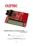
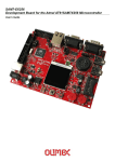
MSP430-5438STK development board
Users Manual
All boards produced by Olimex are ROHS compliant
Rev.A, October 2009
Copyright(c) 2009, OLIMEX Ltd, All rights reserved
Page 1
INTRODUCTION
MSP430-5438STK development board provides easy way for developing and
prototyping with MSP430F5438 mixed signal microcontroller produced by Texas
Instruments.
This powerful microcontroller supports various serial interfaces such as USB
Device, UART, SPI. In addition you will find also audio input and output, debug
interface, LCD, UEXT, two Extensions, mini SD/MMC, User Joystick, User Leds,
Reset button. All this allows you to build a diversity of powerful applications to be
used in a wide range of situations.
BOARD FEATURES
-
CPU: MSP430F5438 mixed signal microcontroller
-
LCD NOKIA 3310 black/white 84x48 pixels
-
JTAG connector
-
JTAG Power_In and Power_Out jumpers
-
Two extension connectors
-
UEXT connector
-
RS232 driver and connector
-
Power plug-in jack for 9V DC power supply
-
Voltage regulator +3.3V – VR1(3.3V)
-
2 status LEDs
-
Power on Led
-
Audio In
-
Audio Out
-
SD/MMC mini connector
-
USB device connector
-
Reset button
-
User joystick
-
PCB: FR-4, 1.5 mm (0,062"), solder mask, silkscreen component print
-
Dimensions: 100x 98mm ( 3.94x 3.85")
Page 2
ELECTROSTATIC WARNING
The MSP430-5438STK board is shipped in protective anti-static packaging. The
board must not be subject to high electrostatic potentials. General practice for
working with static sensitive devices should be applied when working with this
board.
BOARD USE REQUIREMENTS
Cables: The cable you will need depends on the programmer/debugger you use. If
you use MSP430-JTAG, you will need LPT cable, if you use MSP430-JTAG-TINY or
MSP-JTAG-ISO, you will need 1.8m A-B USB cable, if you use MSP430-JTAG-RF,
you can connect it to the USB port of your computer, or via USB cable type A –
female.
Hardware: Programmer/Debugger – one of our Programmers – MSP430-JTAG,
MSP430-JTAG-TINY, MSP430-JTAG-ISO, or MSP430-JTAG-RF.
Software: MSP430 KickStart software.
PROCESSOR FEATURES
MSP430-5438STK board use ultralow-power consumption mixed signal
microcontroller with these features:
–
256KB+512B Flash Memory
–
16KB RAM
–
Four Universal Serial Communication Interfaces
–
Low Supply Voltage Range
–
–
1.8 V to 3.6 V
Ultralow Power Consumption
–
Active Mode (AM): 165 mA/MHz at 8 MHz
–
Standby Mode (LPM3 RTC Mode): 2.60 mA
–
Off Mode (LPM4 RAM Retention): 1.69 mA
–
Shutdown Mode (LPM5): 0.1 mA
–
Wake-Up From Standby Mode in Less Than 5 ms
–
16-Bit RISC Architecture
–
–
Extended Memory
–
18-MHz System Clock
Flexible Power Management System
Page 3
–
–
Fully Integrated LDO With Programmable Regulated Core Supply
Voltage
–
Supply Voltage Supervision, Monitoring, and Brownout
Unified Clock System
–
FLL Control Loop for Frequency Stabilization
–
Low-Power/Low-Frequency Internal Clock Source (VLO)
–
Low-Frequency Trimmed Internal Reference Source (REFO)
–
32-kHz Crystals
–
High-Frequency Crystals up to 32 MHz
–
16-Bit Timer TA0, Timer_A With Five Capture/Compare Registers
–
16-Bit Timer TA1, Timer_A With Three Capture/Compare Registers
–
16-Bit Timer TB0, Timer_B With Seven Capture/Compare Shadow Registers
–
Up to Four Universal Serial Communication Interfaces
–
–
Enhanced UART Supporting Auto-Baudrate Detection
–
IrDA Encoder and Decoder
–
Synchronous SPI
–
I2C™
12-Bit Analog-to-Digital (A/D) Converter
–
Internal Reference
–
Sample-and-Hold
–
Autoscan Feature
–
12 External Channels, 4 Internal Channels
–
Hardware Multiplier Supporting 32-Bit Operations
–
Serial Onboard Programming, No External Programming Voltage Needed
–
Three Channel Internal DMA
–
Basic Timer With Real-Time Clock Feature
Page 4
BLOCK DIAGRAM
Page 5
MEMORY ORGANIZATION
Page 6
USB
NA
C48
NA
C43
100nF
C44+
10uF/6.3V/T ANT
Page 7
P_OUT
HN1x2
2
1
2
1
#LCD_RES
EXT1-28
A_OUT
67
66
65
61
60
59
58
57
MSP430F5438IPZ
P8.7
P8.6/TA1.1
P8.5/TA1.0
P8.4/TA0.4
P8.3/TA0.3
P8.2/TA0.2
P8.1/TA0.1
P8.0/TA0.0
P7.7/A15
P7.6/A14
P7.5/A13
P7.4/A12
P7.3/TA1.2
P7.2/TB0OUTH/SVMOUT
P7.1/XOUT
P7.0/XIN
P6.7/A7
P6.6/A6
P6.5/A5
P6.4/A4
P6.3/A3
P6.2/A2
P6.1/A1
P6.0/A0
P5.7/UCA1RXD/UCA1SOMI
P5.6/UCA1TXD/UCA1SIMO
P5.5/UCB1CLK/UCA1STE
P5.4/UCB1SOMI/UCB1SCL
P5.3/XT2OUT
P5.2/XT2IN
P5.1/VREF-/VEREFP5.0/VREF+/VEREF+
8
7
6
5
56
55
14
13
4
3
2
1
100
99
98
97
54
53
52
51
90
89
10
9
50
49
48
47
46
45
44
43
A_IN
C27
EXT2-33
EXT2-34
3.3VA
39pF
39pF
C26
QCT32768(2x6)/6pF
100k
100k
100k
R34
R35
UCB 0CLK
UCB 0S O MI
C37
47uF/6.3V/TANT
6
4
5
7
8
1
C15
AGND
3.3V
SD/MMC
MICRO
CD/DAT3/CS
CMD/DI
VSS
VDD
CLK/SCLK
DAT0/DO
DAT1/RES
DAT2/RES
10k
1M
C12
470pF
2
3
R22
560R
LED2
LED2
R39
33k
http://www.olimex.com/dev
COPYRIGHT(C), 2009
Rev. A
C14
R23
4.7k
UCA0TXD
UCA0RXD
UCB1SCL
UCB1SDA
UCA1SOMIR26
UCA1SIMO
UCA1CLK
UCA1STE
B<4>
DOWN
C<3>
RIGHT
D<6>
Common<5>
A<1>
E<2>
Center push
UP
LEFT
R42
33k
R46
R43
33k
330R
RIGHT BUT(R)
COMMON
UP BUT(U)
J1
JOYSTICK_MT5_F
BUT(L) LEFT
R41
33k
BH10S
BH10S
BH10S
BH10S
BH10S
BH10S
BH10S
BH10S
BH10S
BH10S
3.3V
UEXT-1
UEXT-2
UEXT-3
UEXT-4
UEXT-5
UEXT-6
UEXT-7
UEXT-8
UEXT-9
UEXT-10
USER JOYSTICK
220R
R24
4.7k
UEXT
AGND
3.3V
SCJ325P00XG0B02G
3-R
2
HEADPHONES
1-L
47uF/6.3V/TANT
C11
AGND
3.3V 3.3V 3.3V
BUT(C) R45 CENTER
330R
BUT(D) DOWN
R40
33k
3.3V
MSP430-5438STK
R21
560R
LED1
LED1
USER LEDS
+
AGND
100nF
47uF/6.3V/TANT
5
8
3-R
2
MICROPHONE
1-L
AGND
47uF/6.3V/TANT
C2
AGND SCJ325P00XG0B02G
C10
AGND
R6
NA
R3
10k
R2
560R
3.3VA
100nF
C6
47pF
R8
100k
C3
R1
100k
3.3VA
U3
TS4871(SO-8)
AGND
3
4
AGND
C7
1uF
R7
20k
AGND
3.3VA
AGND
A_OUT
R5
470k
R12
47k
2.2uF
27k
SD/MMC
UCB 0S TE 2
UCB 0S IMO3
CL470nH/0805/1.76R/250mA
R36
R37
R38
L2
UCB 0CLK
UCB 0S O MI
UCB 0S IMO
UCB 0S TE
6
C1
100nF
AGND
3.3VA
UCA1SOMI,UCA1SIMO,UCA1STE,UCA1CLK,UCB1SDA,UCB1SCL,UCA0RXD,UCA0TXD,CS_SD
100nF
EXT1-34
EXT1-33
EXT1-32
EXT1-31 AGNDAGNDAGND
EXT1-30
EXT1-29
C28
10pF
Q2
C29
10pF
G ND
C24
C25
Q18.000MHz/20pF
Q1
EXT2-26
EXT2-27
EXT2-28
EXT2-29
EXT2-30
EXT2-31
EXT2-32
UCA1SOMI
UCA1SIMO
UCA1STE
UCB1SCL
EXT2-18
EXT2-19
EXT2-20
EXT2-21
EXT2-22
EXT2-23
EXT2-24
EXT2-25
3.3V
EXT2-14
EXT2-15
EXT2-16
EXT2-17
UCB0STE,UCB0SIMO,UCB0CLK,UCB0SOMI
AGND
C13
2.2uF
AGND
R13
33nF
1k
1k
C9
R10
R9
33nF
C8
R11
20k AGND
R15
33k
R4
560R
Z1
BZV55C2V4
Z2
BZV55C2V4
AGND
47pF
C5
A_IN
U2
MCP601-I/SN
AUDIO
GYX-SD-TC0805SYC(YELLOW)
1uF/16V/TANT
ADG8448G(FPA-WZA-08-LF)
C36
EXT1-22
EXT1-23
EXT1-24
EXT1-25
EXT1-26
EXT1-27
P9.7
P9.6
P9.5/UCA2RXD/UCA2SOMI
P9.4/UCA2TXD/UCA2SIMO
P9.3/UCB2CLK/UCA2STE
P9.2/UCB2SOMI/UCB2SCL
P9.1/UCB2SIMO/UCB2SDA
P9.0/UCB2STE/UCA2CLK
P10.7
P10.6
P10.5/UCA3RXD/UCA3SOMI
P10.4/UCA3TXD/UCA3SIMO
P10.3/UCB3CLK/UCA3STE
P10.2/UCB3SOMI/UCB3SCL
P10.1/UCB3SIMO/UCB3SDA
P10.0/UCB3STE/UCA3CLK
P4.7/TB0CLK/SMCLK
P4.6/TB0.6
P4.5/TB0.5
P4.4/TB0.4
P4.3/TB0.3
P4.2/TB0.2
P4.1/TB0.1
P4.0/TB0.0
UCB1SDA
UCA1CLK
UCA0RXD
UCA0TXD
UCB0CLK
UCB0SOMI
UCB0SIMO
UCB0STE
EXT2-6
EXT2-7
EXT2-8
EXT2-9
EXT2-10
EXT2-11
EXT2-12
EXT2-13
0R(NA)
+
LCD
75
74
73
72
71
70
69
68
83
82
81
80
79
78
77
76
P11.2/SMCLK
P11.1/MCLK
P11.0/ACLK
TEST/SBWTCK
#RST/NMI/SBW/TDIO
PJ.3/TCK
PJ.2/TMS
PJ.1/TDI/TCLK
PJ.0/TDO
P3.7/UCB1SIMO/UCB1SDA
P3.6/UCB1STE/UCA1CLK
P3.5/UCA0RXD/UCA0SOMI
P3.4/UCA0TXD/UCA0SIMO
P3.3/UCB0CLK/UCA0STE
P3.2/UCB0SOMI/UCB0SCL
P3.1/UCB0SIMO/UCB0SDA
P3.0/UCB0STE/UCA0CLK
42
41
40
39
36
35
34
33
32
31
30
29
28
27
26
25
10uF/6.3V/TANT
+
UCB2CLK
UCB2SIMO
LCD_D/#C
UCB2STE
EXT1-19
EXT1-20
EXT1-21
LCD_D/#C
#LCD_RES
UCA2RXD
UCA2TXD
UCB2CLK
UCB2SOMI
UCB2SIMO
UCB2STE
LED1
LED2
UCA3RXD
UCA3TXD
91
96
TEST
#RST
86
85
84
95
94
93
92
TCK
TMS
TDI
TDO
AVSS
AVCC
P2.7/ADC12CLK/DMAE0
P2.6/ACLK
P2.5
P2.4/RTCCLK
P2.3/TA1.2
P2.2/TA1.1
P2.1/TA1.0
P2.0/TA1CLK/MCLK
EXT2-4
EXT2-5
0R
1
2
3
4
5
6
7
8
3.3V
TCK
TMS
TDI
TDO
EXT1-11
EXT1-12
EXT1-13
EXT1-14
EXT1-15
EXT1-16
EXT1-17
EXT1-18
EXT1-8
EXT1-9
EXT1-10
12
11
100nF
AGND
C23
VCORE
DVSS1
DVSS2
DVSS3
DVSS4
EXT2-3
6 PC_DSR
7 PC_RTS
8 PC_CTS
9
R32
G2
NA
G1
NA
RS232
DB9-F
1
2
3
4
5
0R
VDD
SCK
SDIN
D/#C
#SCE
GND
VOUT
#RES
R29
33k
NA
#RST
EXT1-4
EXT1-5
EXT1-6
EXT1-7
C22
10uF/6.3V/TANT
62
15
63
37
88
BUT(L)
BUT(R)
BUT(C)
BUT(U)
BUT(D)
PC_RXD
PC_TXD
PC_DTR
C32
100nF
C34
100nF
R33
0R(NA)
LCD
R28
33k
R18
100nF
100nF
FB0805/600R/200mA(201209-601)
L1
C19
C18
C21
470nF
100nF
C17
24
23
22
21
20
19
18
17
13
8
14
7
6
2
R19
R27
33k
BH14S
13
11
9
7
5
3
1
23
22
13
14
12
3.3VA
100nF
C16
R1IN
R2IN
T1OUT
T2OUT
V-
V+
ST3232(SO16)
R1OUT
R2OUT
T1IN
T2IN
C2-
C2+
P1.7
P1.6/SMCLK
P1.5/TA0.4
P1.4/TA0.3
P1.3/TA0.2
P1.2/TA0.1
P1.1/TA0.0
P1.0/TA0CLK/ACLK
12
9
11
10
5
C1-
R20
100nF
P_IN
HN1x2
JTAG
TEST
100nF
14
12
10
8
6
4
2
7
25
33k
GND1
AGND
R17
18
3.3V
GND2
TDI,TDO,TMS,TCK,#RST,TEST
26
21
DEBUG INTERFACE:
CBUS0
CBUS1
CBUS2
CBUS3
CBUS4
TEST
GND3
+
C30
C45
3V3OUT
NC1
#RESET
NC2
OSCI
OSCO
1
5
3
11
2
9
10
6
R30
330R
DVCC4
DVCC3
DVCC2
DVCC1
U1
560R
UCA2RXD R31
UCA2TXD
3
C35 4
100nF
C1+
C33
100nF
GND15
U4PWR
16VCC
R25
3.3V
C49
17
8
19
24
27
28
USBDM
USBDP
FT232RL
R53
NA
R52
+
USB to RS232
10nF
USB_B C50
16
15
TXD
RXD
RTS#
CTS#
DTR#
DSR#
DCD#
RI#
87
38
64
16
#RST
T1107A(6x3.8x2.5mm)
RESET
220R
C31 1
100nF
U4
3.3V
2
7
S H IE LD
0R
0R(NA)
0R(NA)
VCCIO
VCC
FT232RL/SSOP28
VDD_E
CLOSE
2
4
20
1k
PWREN
10uF/6.3V/TANT
3.3V
AGND
C20 2.2nF
GND
0R
10k
VCC
FB /6 0 0 OHM /12 0 6(3 21 6 11 C -6 0 1)
IRLML6402
U5
10uF/6.3V(NA)
R49
+
UCA3TXD
UCA3RXD
GYX-SD-TC0805SURK(RED)
+5V_USB
C47
2
CLOSE
1
100nF
EXT1-2
AGND_E EXT2-2
C40
EXT2-1
C38
GND
C46
2
47uF/6.3V/TANT
100nF
560R
R47
+
1
1
6
1
2 R50
3 R51
4
+
47pF
FET
C42
1
CLOSE
1N4148
390R/1%
240R/1%
PWR
R14
33k
R16
RS232
C4
R48
C41
100nF
R44
1
4
L3
OUT
2
IN
D1
ADJ/GND
3.3VA_E
EXT1-1
RESET CIRCUIT
3.3V 3.3V
7
+
USB
DB104(SMD)
C39
470uF/16VDC
VR1(3.3V)
LM1117IMPX-ADJ
3.3V_E
CLOSE
3.3VA
+
6VAC
9VDC
1N5819S
G1
3.3V
EXT1-3
YDJ-1134
PWR_JACK
D2
POWER SUPPLY
+5V_USB
SCHEMATIC
33k
GYX-SD-TC0805SGC(GREEN)
UCB2CLK,UCB2SIMO,UCB2SOMI,UCB2STE,LCD_D/#C,#LCD_CS,#LCD_RES
BOARD LAYOUT
POWER SUPPLY CIRCUIT
MSP430-5438STK can take power from three sources:
–
PWR connector where 9 V DC or 6 V AC is applied by external power source.
–
+5V_USB from USB DEV
–
JTAG, when P_IN jumper is closed. Note that the JTAG has current limitations.
The board power consumption is: about 20 mA with all peripherals and
microcontroller running at full speed.
RESET CIRCUIT
MSP430-5438STK reset circuit includes JTAG connector pin 11, EXT1 pin 3,
MSP430F5438 pin 96 and Reset button.
CLOCK CIRCUIT
Quartz crystal 32768 MHz is connected to MSP430F5438 pin 13(P7.0/XIN) and pin
14 (P7.1/XOUT).
Quartz crystal 18 MHz is connected to MSP430F5438 pin 89 (P5.2/XT2IN) and pin
90 (P5.3/XT2OUT).
Page 8
JUMPER DESCRIPTION
Power In jumper:
P_IN jumper connects power supply from JTAG connector. You have to
ensure that your circuit doesn't draw more than few milliampers current or the
power supply may decrease due to the JTAG port current limitations. P_IN is
useful and must be used mostly to program the microcontroller.
Power Out jumper:
P_OUT jumper connects power from MSP430-5438STK to JTAG connector.
When this jumper cap is placed, the power supply of JTAG connector will follow
the power supply of the board. This is useful when your board works at lower than
+3,3V power supply.
Note:
P_IN and P_OUT jumper caps should not be placed at the same time.
VDD_E
Enable MSP430F5438 3.3 V power supply.
Default state is closed.
3.3V_E
Enable 3.3V board power supply.
Default state is closed.
3.3VA_E
Enable 3.3V board analog power supply.
Default state is closed.
AGND_E
Enable board analog ground.
Default state is closed.
Input/Output
User joystick with name J1 – this is 4 directions plus center button, in the schematic
the joystick four directions switches are connected: UP, DOWN, LEFT, RIGHT through 33k resistors and CENTER through serial connected 330 and 33k resistors
to 3.3V.
Status LED (green) with name LED1 connected to MSP430F5438 pin 83 (P10.7).
Status LED (yellow) with name LED2 connected to MSP430F5438 pin 82 (P10.6).
Power supply LED (red) with name PWR – indicates that external power source is
applied and board power supply is applied.
Reset button with name RESET, connected to MSP430F5438 pin 96.
LCD black/white 84x48 pixels
Page 9
CONNECTOR DESCRIPTIONS
JTAG
Pin #
Signal Name
Pin #
Signal Name
1
TDO
2
VCC_IN
3
TDI
4
VCC_OUT
5
TMS
6
NC
7
TCK
8
TEST
9
GND
10
NC
11
#RST
12
NC
13
NC
14
NC
RS232
Pin #
Signal Name
1
NC
2
PC_RXD
3
PC_TXD
4
PC_DTR
5
GND
6
PC_DSR
7
PC_RTS
8
PC_CTS
9
NC
Page 10
USB DEV
Pin #
Signal Name
1
+5V_USB
2
USBDM
3
USBDP
4
GND
PWR_JACK
Pin #
Signal Name
1
Power Input
2
GND
UEXT
Pin #
Signal Name
1
3.3V
2
GND
3
UCA0TXD
4
UCA0RXD
5
UCB1SCL
6
UCB1SDA
7
UCA1SOMI
8
UCA1SIMO
9
UCA1CLK
10
UCA1STE
Page 11
EXT1
Pin #
Signal Name
Pin #
Signal Name
1
3.3V
2
GND
3
#RST
4
TCK
5
TMS
6
TDI
7
TDO
8
P11.2
9
P11.1
10
P11.0
11
LED1
12
LED2
13
UCA3RXD
14
UCA3TXD
15
P10.3
16
P10.2
17
P10.1
18
P10.0
19
UCB2CLK
20
UCB2SOMI
21
UCB2SIMO
22
P8.7
23
P8.6
24
P8.5
25
P8.4
26
P8.3
27
P8.2
28
P8.0
29
P7.2
30
P7.3
31
P7.4
32
P7.5
33
P7.6
34
P7.7
Page 12
EXT2
Pin # Signal Name
Pin # Signal Name
1 3.3VA
2 AGND
3 P1.7
4 P1.1
5 P1.0
6 P2.7
7 P2.6
8 P2.5
9 P2.4
10 P2.3
11 P2.2
12 P2.1
13 P2.0
14 UCB0CLK
15 UCB0SOMI
16 UCB0SIMO
17 UCB0STE
18 P4.7
19 P4.6
20 P4.5
21 P4.4
22 P4.3
23 P4.2
24 P4.1
25 P4.0
26 P6.6
27 P6.5
28 P6.4
29 P6.3
30 P6.2
31 P6.1
32 P6.0
33 P5.0
34 P5.1
Page 13
SD/MMC
Pin #
Signal Name
1
Pull-up
2
UCB0STE
3
UCB0SIMO
4
VDD (power supply)
5
UCB0CLK
6
GND
7
UCB0SOMI
8
Pull-up
9
Not connected
10
Not connected
11
Not connected
12
Not connected
Microphone
Pin #
Signal Name
1
AGND
2
NC
3
MIC
Headphone
Pin #
Signal Name
1
AGND
2
IN1=IN2
3
IN2=IN1
Page 14
MECHANICAL DIMENSIONS
Page 15
AVAILABLE DEMO SOFTWARE
–
Display demo
–
LEDs and Buttons demo
–
SD/MMC demo
–
UART demo
–
USB UART demo
–
ADC and DAC demo
Page 16
ORDER CODE
MSP430-5438STK – assembled and tested (no kit, no soldering required)
How to order?
You can order to us directly or by any of our distributors.
Check our web www.olimex.com/dev for more info.
Revision history:
REV.A -
October 2009
Initial release
REV. B -
March 2012
Changes:
Page 13 -
Changed wrong signal names in the table with the correct ones (signals #14,15,16,17)
Page 17
Disclaimer
© 2009 Olimex Ltd. All rights reserved. Olimex®, logo and combinations thereof, are registered trademarks of
Olimex Ltd. Other terms and product names may be trademarks of others.
The information in this document is provided in connection with Olimex products. No license, express or implied
or otherwise, to any intellectual property right is granted by this document or in connection with the sale of
Olimex products.
Neither the whole nor any part of the information contained in or the product described in this document may be
adapted or reproduced in any material from except with the prior written permission of the copyright holder.
The product described in this document is subject to continuous development and improvements. All particulars
of the product and its use contained in this document are given by OLIMEX in good faith. However all warranties
implied or expressed including but not limited to implied warranties of merchantability or fitness for purpose are
excluded.
This document is intended only to assist the reader in the use of the product. OLIMEX Ltd. shall not be liable for
any loss or damage arising from the use of any information in this document or any error or omission in such
information or any incorrect use of the product.
Page 18