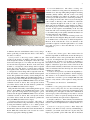
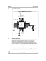
1
C ALIFORNIA S TATE U NIVERSITY S ACRAMENTO DARK INERTIAL MAPPING: E ND OF P ROJECT D OCUMENTATION Authors: Andre J ULIEN Yan L IN Alexander M EADOWS Joseph YOUNGBLOOD Instructor: Professor TATRO May 03, 2015 i C ONTENTS Abstract 1 Index Terms 1 I Introduction 1 II Design Idea and Revised Societal Problem II-A Design Idea Contract . . . . . . . . . . . II-A1 Background . . . . . . . . . . II-A2 Inertial Navigation . . . . . . . II-A3 Feature Set . . . . . . . . . . . II-A4 Feature: Self-Referential . . . II-A5 Feature: Wearable . . . . . . . II-A6 Feature: Local Data Storage . II-A7 Feature: Visualization Software II-A8 Current Implementations . . . II-A9 Dead-Reckoning Mitigation . . II-B Revised Societal Problem . . . . . . . . . II-C Market Review . . . . . . . . . . . . . . . II-C1 Public Sector . . . . . . . . . . II-C2 Private Sector . . . . . . . . . II-C3 Market Competition . . . . . . II-C4 Market Penetration . . . . . . . . . . . . . . . . . . . . . . . . . . . . . . . . . . . . . . . . . . . . . . . . . . . . . . . . . . . . . . . . . . . . . . . . . . . . . . . . . . . . . . . . . . . . . . . . . . . . . . . . . . . . . . . . . . . . . . . . . . . . . . . . . . . . . . . . . . . . . . . . . . . . . . III Financial Responsibility IV Work Breakdown Structure IV-A Self-Referential . . . . . . . . . . . . . . . . . . . . . . . IV-A1 Read Sensor Data . . . . . . . . . . . . . . . . IV-A2 Calculating Position from Data . . . . . . . . . IV-A3 Test Accuracy . . . . . . . . . . . . . . . . . . IV-B Wearable . . . . . . . . . . . . . . . . . . . . . . . . . . . IV-B1 Build Components on breadboard . . . . . . . IV-B2 Battery Implementation . . . . . . . . . . . . . IV-B3 Create Housing . . . . . . . . . . . . . . . . . IV-B4 Field Testing . . . . . . . . . . . . . . . . . . . IV-C Stores Data Locally . . . . . . . . . . . . . . . . . . . . . IV-C1 Select file format . . . . . . . . . . . . . . . . IV-C2 Connect SD shield to microcontroller . . . . . IV-C3 Test file compatibility with software . . . . . . IV-C4 Make a button to enable/disable data recording IV-D Software . . . . . . . . . . . . . . . . . . . . . . . . . . . IV-D1 Data Manipulation . . . . . . . . . . . . . . . . IV-D2 Drawing . . . . . . . . . . . . . . . . . . . . . IV-D3 Graphical User Interface . . . . . . . . . . . . IV-D4 Debugging . . . . . . . . . . . . . . . . . . . . IV-D5 Deployment . . . . . . . . . . . . . . . . . . . V Target Deadlines VI Risk Assessment VI-A Severe . VI-A1 VI-A2 VI-A3 VI-A4 VI-A5 . . . . . . . . . . . . . . . . . . . . . . . . . . . . . . . . . . . . . . . . . . . . . . . . . . . . . . . . . . . . . . . . . . . . . . . . . . . . . . . . . . . . . . . . . . . . . . . . . . . . . . . . . . . . . . . . . . . . . . . . . . . . . . . . . . . . . . . . . . . . . . . . . . . . . . . . . . . . . . . . . . . . . . . . . . . . . . . . . . . . . . . . . . . . . . . . . . . . . . . . . . . . . . . . . . . . . . . . . . . . . . . . . . . . . . . . . . . . . . . . . . . . . . . . . . . . . . . . . . . . . . . . . . . . . . . . . . . . . . . . . . . . . . . . . . . . . . . . . . . . . . . . . . . . . . . . . . . . . . . . . . . . . . . . . . . . . . . . . . . . . . . . . . . . . . . . . . . . . . . . . . . . . . . . . . . . . . . . . . . . . . . . . . . . . . . . . . . . . . . . 1 2 2 2 2 2 3 3 3 4 4 4 5 5 6 6 7 8 . . . . . . . . . . . . . . . . . . . . . . . . . . . . . . . . . . . . . . . . . . . . . . . . . . . . . . . . . . . . . . . . . . . . . . . . . . . . . . . . . . . . . . . . . . . . . . . . . . . . . . . . . . . . . . . . . . . . . . . . . . . . . . . . . . . . . . . . . . . . . . . . . . . . . . . . . . . . . . . . . . . . . . . . . . . . . . . . . . . . . . . . . . . . . . . . . . . . . . . . . . . . . . . . . . . . . . . . . . . . . . . . . . . . . . . . . . . . . . . . . . . . . . . . . . . . . . . . . . . . . . . . . . . . . . . . . . . . . . . . . . . . . . . . . . . . . . . . . . . . . . . . . . . . . . . . . . . . . . . . . . . . . . . . . . . . . . . . . . . . . . . . . . . . . . . . . . . . . . . . . . . . . . . . . . . . . . . . . . . . . . . . . . . . . . . . . . . . . . . . . . . . . . . . . . . . . . . . . . . . . . . . . . . . . . . . . . . . . . . . . . . . . . . . . . . . . . . . . . . . . . . . . . . . . . . . . . . . . . . . . . . . . . . . . . . . . . . . . . . . 8 8 8 9 10 11 11 11 12 12 13 13 13 13 13 13 13 13 13 14 14 14 . . . . . . . . . . . . . . . . . . . . . . Lose Accuracy Due to Drift . . . . . Design Unable to Meet Expectations . Positional Measurements Unavailable Overworked/Exhaustion . . . . . . . . Lack of In-house Skill . . . . . . . . . . . . . . . . . . . . . . . . . . . . . . . . . . . . . . . . . . . . . . . . . . . . . . . . . . . . . . . . . . . . . . . . . . . . . . . . . . . . . . . . . . . . . . . . . . . . . . . . . . . . . . . . . . . . . . . . . . . . . . . . . . . . . . . . . . . . . . . . . . . . . . . . . . . . . . . . . . . . . . . . . . . . . . . . . . . . . . . . . . . . 14 14 14 15 15 15 15 ii VI-B VI-C VI-D VII Major . . VI-B1 VI-B2 VI-B3 VI-B4 VI-B5 Medium VI-C1 VI-C2 VI-C3 VI-C4 VI-C5 Minor . VI-D1 VI-D2 VI-D3 VI-D4 VI-D5 . . . . . . . . . . . . . . . . . . . . . . . . . . . Feature Exceeds Time Quota . . . . . . . . . . Software Incompatibility . . . . . . . . . . . . Communication Breakdown . . . . . . . . . . . Insufficient Hardware . . . . . . . . . . . . . . Delay do to non-project priorities . . . . . . . . . . . . . . . . . . . . . . . . . . . . . . . . . . Hive Down . . . . . . . . . . . . . . . . . . . . File Structure Exceeds Filestructure Limitations Interface Unintuitive . . . . . . . . . . . . . . . Financial Burden . . . . . . . . . . . . . . . . Ideal Sampling Rate Unattainable . . . . . . . . . . . . . . . . . . . . . . . . . . . . . . . . . . Team Member Absence . . . . . . . . . . . . . Power Consumption Concerns/Expectations . . Equipment Loss . . . . . . . . . . . . . . . . . Personal Computer Failure . . . . . . . . . . . Data Hosting Downtime . . . . . . . . . . . . . . . . . . . . . . . . . . . . . . . . . . . . . . . . . . . . . . . . . . . . . . . . . . . . . . . . . . . . . . . . . . . . . . . . . . . . . . . . . . . . . . . . . . . . . . . . . . . . . . . . . . . . . . . . . . . . . . . . . . . . . . . . . . . . . . . . . . . . . . . . . . . . . . . . . . . . . . . . . . . . . . . . . . . . . . . . . . . . . . . . . . . . . . . . . . . . . . . . . . . . . . . . . . . . . . . . . . . . . . . . . . . . . . . . . . . . . . . . . . . . . . . . . . . . . . . . . . . . . . . . . . . . . . . . . . . . . . . . . . . . . . . . . . . . . . . . . . . . . . . . . . . . . . . . . . . . . . . . . . . . . . . . . . . . . . . . . . . . . . . . . . . . . . . . . . . . . . . . . . . . . . . . . . . . . . . . . . . . . . . . . . . . . . . . . . . . . . . . . . . . . . . . . . . . . . . . . . . . . . . . . . . . . . . . . . . . . Tasks Completed in Fall 2014 User Manual IX-A Device Usage Overview . . . . IX-B Limitations . . . . . . . . . . . IX-B1 Accuracy . . . . . . IX-B2 Usability Conditions IX-B3 Run-time . . . . . . 15 15 15 15 15 15 16 16 16 16 16 16 16 16 16 16 16 17 17 VIII Tasks Undertaken in Spring 2015 VIII-A Problem Statement Revision . . . . . . . . . . VIII-B Device Test Plan . . . . . . . . . . . . . . . . . VIII-C Market Review . . . . . . . . . . . . . . . . . . VIII-D Mid-Term Progress Review . . . . . . . . . . . VIII-E Feature Presentations and Reports . . . . . . . VIII-F Deployable Prototype Review . . . . . . . . . . VIII-G End of Project Documentation . . . . . . . . . VIII-H Self-Referential . . . . . . . . . . . . . . . . . VIII-H1 Sensor Selection . . . . . . . . . . . VIII-H2 Establish Kinematic Model . . . . . VIII-H3 Interface Devices . . . . . . . . . . VIII-H4 Device Testing . . . . . . . . . . . . VIII-I Local Data Storage . . . . . . . . . . . . . . . VIII-I1 Implement Data Storage Protocol . . VIII-I2 New Search Session . . . . . . . . . VIII-J Software . . . . . . . . . . . . . . . . . . . . . VIII-J1 Camera Rotation . . . . . . . . . . . VIII-J2 Menu . . . . . . . . . . . . . . . . . VIII-J3 Exit . . . . . . . . . . . . . . . . . . VIII-J4 Load . . . . . . . . . . . . . . . . . VIII-J5 Display . . . . . . . . . . . . . . . . VIII-J6 Draw position point on 3 axis space VIII-J7 Lines . . . . . . . . . . . . . . . . . VIII-J8 Compile Code . . . . . . . . . . . . VIII-K Wearability . . . . . . . . . . . . . . . . . . . . VIII-K1 3D print housing . . . . . . . . . . . VIII-K2 Battery selection . . . . . . . . . . . VIII-K3 Integrate Device into Housing . . . VIII-K4 Performance Testing . . . . . . . . . IX . . . . . . . . . . . . . . . . . . . . . . . . . . . . . . . . . . . . . . . . . . . . . . . . . . . . . . . . . . . . . . . . . . . . . . . . . . . . . . . . . . . . . . . . . . . . . . . . . . . . . . . . . . . . . . . . . . . . . . . . . . . . . . . . . . . . . . . . . . . . . . . . . . . . . . . . . . . . . . . . . . . . . . . . . . . . . . . . . . . . . . . . . . . . . . . . . . . . . . . . . . . . . . . . . . . . . . . . . . . . . . . . . . . . . . . . . . . . . . . . . . . . . . . . . . . . . . . . . . . . . . . . . . . . . . . . . . . . . . . . . . . . . . . . . . . . . . . . . . . . . . . . . . . . . . . . . . . . . . . . . . . . . . . . . . . . . . . . . . . . . . . . . . . . . . . . . . . . . . . . . . . . . . . . . . . . . . . . . . . . . . . . . . . . . . . . . . . . . . . . . . . . . . . . . . . . . . . . . . . . . . . . . . . . . . . . . . . . . . . . . . . . . . . . . . . . . . . . . . . . . . . . . . . . . . . . . . . . . . . . . . . . . . . . . . . . . . . . . . . . . . . . . . . . . . . . . . . . . . . . . . . . . . . . . . . . . . . . . . . . . . . . . . . . . . . . . . . . . . . . . . . . . . . . . . . . . . . . . . . . . . . . . . . . . . . . . . . . . . . . . . . . . . . . . . . . . . . . . . . . . . . . . . . . . . . . . . . . . . . . . . . . . . . . . . . . . . . . . . . . . . . . . . . . . . . . . . . . . . . . . . . . . . . . . . . . . . . . . . . . . . . . . . . . . . . . . . . . . . . . . . . . . . . . . . . . . . . . . . . . . . . . . . . . . . . . . . . . . . . . . . . . . . . . . . . . . . . . . . . . . . . . . . . . . . . . . . . . . . . . . . . . . . . . . . . . . . . . . . . . . . . . . . . . . . . . . . . . . . . . . . . . . . . . . . . . . . . . . . . . . . . . . . . . . . . . . . . . . . . . . . . . . . . . . . . . . . . . . . . . . . . . . . . . . . . . . . . . . . . . . . . . . . . . . . . . . . . . . . . . . . . . . . . . . . . . . . . . . . . . . . 17 17 17 17 18 18 18 18 18 18 18 19 19 19 19 19 19 19 19 19 19 19 19 19 19 19 19 20 20 20 . . . . . . . . . . . . . . . . . . . . . . . . . . . . . . . . . . . . . . . . . . . . . . . . . . . . . . . . . . . . . . . . . . . . . . . . . . . . . . . . . . . . . . . . . . . . . . . . . . . . . . . . . . . . . . . . . . . . . . . . . . . . . . . . . . . . . . . . . . . . . . . . . . . . . . . . . . . 20 20 20 20 20 20 iii IX-C IX-D IX-E IX-F IX-B4 Memory Card . . . . . . . Hardware Usage . . . . . . . . . . . . IX-C1 Memory Card . . . . . . . IX-C2 Battery Install Instructions IX-C3 User Attachment . . . . . . IX-C4 Data Gathering Activation Software Usage . . . . . . . . . . . . Hardware Components . . . . . . . . Software Components . . . . . . . . . . . . . . . . . . . . . . . . . . . . . . . . . . . . . . . . . . . . . . . . . . . . . . . . . . . . . . . . . . . . . . . . . . . . . . . . . . . . . . . . . . . . . . . . . . . . . . . . . . . . . . . . . . . . . . . . . . . . . . . . . . . . . . . . . . . . . . . . . . . . . . . . . . . . . . . . . . . . . . . . . . . . . . . . . . . . . . . . . . . . . . . . . . . . . . . . . . . . . . . . . . . . . . . . . . . . . . . . . . . . . . . . . . . . . . . . . . . . . . . . . . . . . . . . . . . . . . . . . . . . . . . . . . . . . . . . . . . . . . . . . . . . . . . . . . . . . . . . . . . . . . . . . . . . . . . . . . . . . . . . . . . . . 20 20 20 20 20 21 21 22 22 X Design Documentation 22 XI Hardware XI-A Block Diagram and Document at Block Level . . . . . . . . . . . . . . . . . . . . . . . . . . . . . . . . XI-B Schematics and Documentation to Component Level . . . . . . . . . . . . . . . . . . . . . . . . . . . . 23 23 25 XII Software XII-A Block Diagram and Document at Block Level . . . . . . . . . . . . . . . . . . . . . . . . . . . . . . . . XII-B Flowcharts, Pseudocode, and Documentation to Subroutine Level . . . . . . . . . . . . . . . . . . . . . 27 27 27 XIII Mechanical XIII-A Device Housing Main Body . . . . . . . . . . . . . . . . . . . . . . . . . . . . . . . . . . . . . . . . . XIII-B The Other Parts . . . . . . . . . . . . . . . . . . . . . . . . . . . . . . . . . . . . . . . . . . . . . . . . XIII-C Part Creation . . . . . . . . . . . . . . . . . . . . . . . . . . . . . . . . . . . . . . . . . . . . . . . . . . 28 28 29 29 XIV Test Plan and Test Results for Hardware XIV-A Static Timed Test . . . . . . . . . XIV-A1 Test results . . . . . . . XIV-B Speed Test . . . . . . . . . . . . . XIV-B1 Test Results . . . . . . XIV-C Drop Test . . . . . . . . . . . . . XIV-C1 Test Results . . . . . . XIV-D Crush Test . . . . . . . . . . . . . XIV-D1 Test Results . . . . . . XIV-E Shake Test . . . . . . . . . . . . . XIV-E1 Test Results . . . . . . XIV-F Dissipation Test . . . . . . . . . . XIV-G Moisture Test . . . . . . . . . . . XIV-H Shatter Test . . . . . . . . . . . . XIV-I Battery Runtime Test . . . . . . . XIV-I1 Test Results . . . . . . . . . . . . . . . . . . . . . . . . . . . . . . . . . . . . . . . . . . . . . . . . . . . . . . . . . . . . . . . . . . . . . . . . . . . . . . . . . . . . . . . . . . . . . . . . . . . . . . . . . . . . . . . . . . . . . . . . . . . . . . . . . . . . . . . . . . . . . . . . . . . . . . . . . . . . . . . . . . . . . . . . . . . . . . . . . . . . . . . . . . . . . . . . . . . . . . . . . . . . . . . . . . . . . . . . . . . . . . . . . . . . . . . . . . . . . . . . . . . . . . . . . . . . . . . . . . . . . . . . . . . . . . . . . . . . . . . . . . . . . . . . . . . . . . . . . . . . . . . . . . . . . . . . . . . . . . . . . . . . . . . . . . . . . . . . . . . . . . . . . . . . . . . . . . . . . . . . . . . . . . . . . . . . . . . . . . . . . . . . . . . . . . . . . . . . . . . . . . . . . . . . . . . . . . . . . . . . . . . . . . . . . . . . . . . . . . . . . . . . . . . . . . . . . . . . . . . . . . . . . . . . . . . . . . . . . . . . . . . . . . . . . . . . . . . . . . . . . . . . . . . . . . . . . . . . . . . . . . . . . . . . . . . . . . . . . . . . . . . . . . . . . . . . . . . . . . . . . . . . . . . . . . . . . . . . 29 29 29 29 29 30 30 30 30 30 30 30 30 30 30 31 . . . . . . . . . . . . . . . . . . . . . . . . . . . . . . . . . . . . . . . . . . . . . . . . . . . . . . . . . . . . . . . . . . . . . . . . . . . . . . . . . . . . . . . . . . . . . . . . . . . . . . . . . . . . . . . . . . . . . . . . . . . . . . . . . . . . . . . . . . . . . . . . . . . . . . . . 31 31 31 31 31 . . . . . . . . . . . . . . . . . . . . . . . . . . . . . . . . . . . . . . . . . . . . . . . . . . . . . . . . . . . . . . . . . . . . . . . . . . . . . . . . . . . . . . . . . . . . . . . . . . . . . . . . . . . . . . . . . . . . . . . . . . . . . . . . . . . . . . . . . . . . . . . . . . . . . . . . . . . . . . . . . . . . . . . . . . . . . . . . . . . . . . . . . . . . . . 32 32 32 32 32 32 XVII Record Data File Test XVII-A Test Results . . . . . . . . . . . . . . . . . . . . . . . . . . . . . . . . . . . . . . . . . . . . . . . . . . 33 33 XVIII Overload Test XVIII-A Test Results . . . . . . . . . . . . . . . . . . . . . . . . . . . . . . . . . . . . . . . . . . . . . . . . . . 33 33 XV Test Plan and Test Results for Software XV-A Short Distance Test . . . . . . . . XV-A1 Test Results . . . . . . XV-B Medium Distance Test . . . . . . . XV-B1 Test Results . . . . . . XVI Long Distance Test XVI-2 Test Results XVI-A Unit Test . . . . . . . . XVI-A1 Test Results XVI-B Sample Data Test . . . XVI-B1 Test Results . . . . . . . . . . . . . . . . . . . . . . . . . . . . . . iv XIX Conclusion 33 Glossary 33 References 33 Appendices A B 35 Data sheets . . . . . . . . . . . . . . . . . . . . . . . . . . . . . . . . . . . . . . . . . . . . . . . . . . . 35 Resume . . . . . . . . . . . . . . . . . . . . . . . . . . . . . . . . . . . . . . . . . . . . . . . . . . . . . 140 L IST OF F IGURES 1 2 3 4 5 6 7 8 9 10 11 12 13 14 15 16 17 HMC-6343 Three-Axis Compass (By: Team D.I.M.) . . . . . . . . . . . . . . . . . Device Interior (By: Team D.I.M.) . . . . . . . . . . . . . . . . . . . . . . . . . . . Device Strap Back (By: Team D.I.M.) . . . . . . . . . . . . . . . . . . . . . . . . . Device Active Front (By: Team D.I.M.) . . . . . . . . . . . . . . . . . . . . . . . . UI Functionality Navigation taken by team D.I.M. . . . . . . . . . . . . . . . . . . UI Functionality Run Color (By: Team D.I.M.) . . . . . . . . . . . . . . . . . . . . Basic Data flow (By: Team D.I.M.) . . . . . . . . . . . . . . . . . . . . . . . . . . Basic Step Calculation (By: Team D.I.M.) . . . . . . . . . . . . . . . . . . . . . . . Basic Step Calculation (By: Team D.I.M.) . . . . . . . . . . . . . . . . . . . . . . . Main case body (By: Team D.I.M.) . . . . . . . . . . . . . . . . . . . . . . . . . . Main case, the other parts (By: Team D.I.M.) . . . . . . . . . . . . . . . . . . . . . Static Time Test . . . . . . . . . . . . . . . . . . . . . . . . . . . . . . . . . . . . . Drop Test resulted in a fracture in the enclosure (By: Team D.I.M.) . . . . . . . . . Short Distance Test around center tables in 3001 Riverside Hall (By: Team D.I.M.) Line Test (By: Team D.I.M.) . . . . . . . . . . . . . . . . . . . . . . . . . . . . . . Medium Distance Test on 3rd Floor Hallway, Riverside Hall (By: Team D.I.M.) . . Long Distance Test between Riverside Hall and Sequoia Hall (By: Team D.I.M.) . . . . . . . . . . . . . . . . . . . . . . . . . . . . . . . . . . . . . . . . . . . . . . . . . . . . . . . . . . . . . . . . . . . . . . . . . . . . . . . . . . . . . . . . . . . . . . . . . . . . . . . . . . . . . . . . . . . . . . . . . . . . . . . . . . . . . . . . . . . . . . . . . . . . . . . . . . . . . . . . . . . . . . . . . . . . . . . . . . . . . . . . . . . . . . . . . . . . . . . . . . . . . . . . . . . . . . . . . . . . . . . . . . . . . . . . . . . . . . . . . . . . . . . . . . . . . . . . . . . . . . . . . . . . . . . . . 15 20 21 21 21 21 27 27 27 29 29 29 30 31 31 31 32 Product pricing . . . . . . . . . . . . . . . . . . . . . . . . . . . . . . . . . . . . . . Feature: Documentation Deadlines and Completion Dates . . . . . . . . . . . . . . . Feature: Self-Referential Deadlines and Completion Dates . . . . . . . . . . . . . . . Feature: Local Data Storage Deadlines and Completion Dates . . . . . . . . . . . . . Feature: Software Deadlines and Completion Dates . . . . . . . . . . . . . . . . . . Feature: Wearability - Deadlines and Completion Dates . . . . . . . . . . . . . . . . Feature: Self-Referential Fall 2014 Completed Tasks with Hour Allocation . . . . . Feature: Local Data Storage Fall 2014 Completed Tasks with Hour Allocation . . . Feature: Wearable Fall 2014 Completed Tasks with Hour Allocation . . . . . . . . Feature: Software Fall 2014 Completed Tasks with Hour Allocation . . . . . . . . . Completed Course Assignments Fall 2014 Individual Member Contributions . . . . Feature: Documentation Spring 2015 Completed Tasks with Hour Allocation . . . . Feature: Software - Spring 2015 - Completed Tasks with Hour Allocation . . . . . . Feature: Local Data Storage - Spring 2015 - Completed Tasks with Hour Allocation . Feature: Wearability - Spring 2015 - Completed Tasks with Hour Allocation . . . . . . . . . . . . . . . . . . . . . . . . . . . . . . . . . . . . . . . . . . . . . . . . . . . . . . . . . . . . . . . . . . . . . . . . . . . . . . . . . . . . . . . . . . . . . . . . . . . . . . . . . . . . . . . . . . . . . . . . . . . . . . . . . . . . . . . . . . . . . . . . . . . . . . . . . . . . . . . . . . . . . . . . . . . . . . . . . . . . . . . . . . . . . . . . . . . . . . . . . . . . . . . . . . . . . . . . . . . . . . . . . . . . . . 8 14 14 14 14 14 17 17 17 17 17 18 18 18 18 L IST OF TABLES I II III IV V VI VII VIII IX X XI XII XIII XIV XV 1 Dark Inertial Mapping: End of Project Documentation Andre Julien∗ , Yan Lin† , Alexander Meadows‡ and Joseph Youngblood§ Department of Computer and Electrical Engineering, California State University Sacramento Sacramento, CA USA ∗ † Email: [email protected], [email protected], ‡ [email protected], § [email protected] Abstract—Search and rescue personnel typically conduct operations within under two categories: field search, and coordination management. In urban environments where building geometry contributes to signal dampening and reflection, popular localization methodologies such as GPS cannot be employed effectively. The Dark Inertial Mapping system seeks to address technical deficiencies seen within the popular methods of search and rescue under these circumstances. This is accomplished using a hip-mounted wearable device that utilizes a PDR algorithm to generate displacement, allowing for the search coordinator to analyze and efficiently deploy consequent searches, to search efficiency. The wearable device generates and stores displacement data, and includes accompanying software dedicated to the visual interpretation of device data. The intended aim for such a system to provide a better level of search path information regarding field search personnel to the search coordination manager. By reducing path redundancy, the device aims to save more lives through enhancing search coordination efficiency. Index Terms—test process, tests results, self referential, wearability, data storage, software testing, mapping. I. I NTRODUCTION Urban Search and Rescue is the location, extraction, of and provision of aid to civilians trapped in confined spaces [1]. Organizations such as FEMA have implemented infrastructures to expedite these search efforts through division of labor based on the nature of work performed. The two primary roles associated with the execution of search activity are Task Forces and Incident Support teams [1]. With the assistance of technology, these teams are capable of coordinating to efficiently relay information regarding a catastrophic event. However in urban areas, satellite-based localization technology such as GPS have proven to be unreliable due to signal dampening and reflection caused by building geometry. In these situations, PDR-based localization algorithms are typically employed [2]. Realizing the difficulties of of generating search paths explicitly from memory and verbal exchange, Team DIM comprising of Andre Julien, Yan Lin, Alexander Meadows, and Joseph Youngblood set out to create a passive, wearable device capable of generating, and approximating search path data from Urban Search and Rescue task forces. To further enhance the results of search efforts, a complementary software visualization aspect was built intended for use by Incident Support teams to aggregate the search data generated by these devices into a visual model. Initially the team focused primarily on implementing kinematic model based on double integration of accelerometer data. Due to complications that arose as the result of non-uniform rotational data, in conjunction with accumulated error over time, the kinematic model required drastic revisions in order to fall within the drafted featureset within the Design Idea Contract. Based on research conducted involving Pedestrian dead-reckoning systems, the system’s kinematic model was changed to record and interpret human gait motion. Based off of the testing performed, the final product was capable of generating paths with an error of 5% over 90 meters. The aim such a system for Search and Rescue efforts in urban search environments would contribute toward the increase the number of lives saved by reducing search path redundancy in consequently scheduled searches. II. D ESIGN I DEA AND R EVISED S OCIETAL P ROBLEM Initial research conducted during the Fall semester of 2014 showed that there was a compelling societal need for the improvement of Search and Rescue operator protocol. Key resources of interest included topical journal review spanning topics from coordinated robotic search and rescue to SWAT team coordination protocol. Based on the information found, a solution to meet the technical needs of Search and Rescue teams was proposed in form of the Design Idea Contract. For counsel regarding field operations and standard operating procedure, the team consulted Ray Stedronsky, a retired Captain from Truck 106 Metro Fire with more than three decades of field experience. Due to technical issues that occurred during the Fall Project Semester, the team required a change in kinematic model in order to meet the original contractual obligation detailed under the Design Idea Contract by the term deadline. The original kinematic model was based on translational motion, assuming a static orientation of the device itself. To calculate displacement, the device recorded acceleration data to external storage. Due to the low throughput of the AtMega328 platform, data was postprocessed in the visualization software in order to maximize sampling rate of sensors. However, this led to the requirement of rapid orientation analysis to determine the linear acceleration with respect to the frame of reference of the earth. Critical issues consisted of poor sampling rate, accumulated error in integration of accelerometer data, non-symmetrical heading, along with a large number of corner cases attributed to device orientation. To mitigate the risks associated with an undeliverable design, the project switched from the original intent of double-integration of acceleration data to a revised 2 implementation utilizing a dead reckoning algorithm. During the spring semester, a market review was also conducted, assessing and reviewing previous attempts by other teams to address similar issues in coordination of Search and Rescue efforts. A. Design Idea Contract 1) Background: Based on research conducted by Team DIM, it was made evident that the condition of ”Lost or Disoriented” was considered an impactful cause of loss of life for first-response emergency personnel. Publications released by FEMA between the years of 2003 and 2012 provided the statistics of fatalities. In these annual reports [3] , the U.S. Fire Administration listed ”Lost or Disoriented” as a category for nature of fatality, containing resulting cause of fatality as a result of these factors. Within the given years of the reports, 10 personnel fatalities were reported in structure fire incidents, where the nature of fatality was due to being lost or disoriented. The nature of the deaths was primarily due to asphyxiation. . With the population increase in urban areas and the age and condition of buildings, there is an increasing concern of death and injury in the case of a catastrophic event. ”The University of California has released to Los Angeles city officials a list of about 1,500 old concrete buildings that are potentially at risk of collapse during an earthquake [4].” Compounded with predictions that catastrophic events will increase, more effective and reliable technologies are necessary to assist Search and Rescue personnel. ”We predict that the number of earthquakes with death tolls greater than 100,000 (50,000) will increase in the 21st century to 8.73.3 (20.5 4.3 from 4 (7) observed in the 20th century..” [5] These figures suggested an increase in Search and Rescue missions that will require planning and coordination among rescue teams searching through buildings. ”Collapsed structure rescue work is dangerous, even with optimal safety practices (being able to accurately determine when further risk becomes unwarranted, may minimize overall risk to rescuers)” [6] With inefficient or nonexistent monitoring of rescue personnel there is no information about what locations were searched, so it would not be uncommon for an area to be searched repeatedly putting the rescuers in undue risk. With accurate information, search and rescue teams can quickly find holes in their patterns to ensure that all locations are checked. 2) Inertial Navigation: As a result of the research conducted, Team DIM was opted to devise a solution that would assist rescuers in expediting the extraction process of victims, preventing unnecessary deaths due to unfamiliar environments, low vision, or disorientation. As an initial point of contact, the members of Team DIM contacted Captain Ray Stedronsky. The initial correspondence provided insight for the standard operating procedures that are typically employed for search and rescue operations in interior environments [7]. In these situations, the priority is placed on covering as much ground as fast as possible due to the rapidly diminishing survival conditions. Search and rescue responders are paired, and typically use a right-hand method to traverse hallways until they can find a room. When a room is located, one rescuer stays at the door, while the other checks the room, and acts as an exit beacon for their partner. For large areas, a long rope (typically 200 feet) is used with segmented knots every 50 feet. This rope is anchored to a sturdy point at the entry area. A 20 secondary foot-rope with a metal ring at the end is affixed to the rescuer, and the larger rope is inserted through the ring. The knot/ring sequence presents a rough estimation of distance every 50 feet, and ensures that the operative does not stray too far from the rope leading to the exit. These methods have been a long-standing navigation methods in the search and rescue field, as they have proved reliable given typical interior design methodologyIf a wall is followed continuously, the navigator should return to their starting point. Additionally, they require no dependence on external sources. Using these principles, Team DIM sought out to make a device was both capable of determining displacement, as well as providing a rudimentary map of the path traveled. 3) Feature Set: Upon establishing that the loss of life due to unfamiliar environments or lack of orientation was a valid concern, Team DIM was tasked with the creation of a device that would address the needs of rescue personnel and provide them a device that would expedite their efforts. The features highlighted in the Design Idea Contract consisted of the following: -Self-Referential -Wearable -Local Data Storage -Visualization Software 4) Feature: Self-Referential: One of the key features of Project DIM is the capability to generate position from solely the data provided from the devices inertial measurement unit. Self Referential devices do not rely on any outside information to provide accurate output. Our device is self referential and uses no outside signals to interpret where it is from an arbitrary starting location. This feature will be referred to as SelfReferential Position Calculation. To fully utilize this feature, it necessitates the utilization of collected data to generate a positional calculation from an initial start position. The best way to understand a feature is to understand the decisions made during its implementation. As our project started it was observed that communication in emergency situation can be unobtainable. It was noted that there were several issues with devices that attempted to communicate in these situations and that these devices had been proven unreliable or the equipment was too heavy, bulky, cumbersome, and expensive this led to these devices being left behind due to its inhibiting nature [?]. These issues were problems that wanted to mitigate and Team DIM decided that our device should be a self contained, lightweight, and low-cost system. This meant that the proposed system had to be made up of inexpensive and lightweight parts. Since obtaining signals out of these environments sometime takes a large antenna and a signal generator to send out we were not able to use communication on our device. Team DIMS device will be able to track its position on its own and could not rely on outside communication for assistance or back up. This became the core parameter of our project and was 3 taken as a benchmark of reliability to be self sufficient and require no set up of communication devices during a time of crisis. This would minimize impact on the search and rescue teams who implemented our device. Because the hardware was chosen to be both passive and self referential the only visualization tool was through the software package. Thusly the hardware depends on the software to display its results. The hardware and software choices were made as a joint effort such as choosing the file type and choosing what data is saved. Furthermore when testing the device more requests for functionality were made for the software. These features were added to help testing and typically proved to improve the software. The hardware components were also limited to the specificity that they could be wearable. This meant that large and bulky equipment could not be added to the hardware even though initial prototypes had a laptop connected. This also meant that the hardware in order to be self sufficient needed to have its own power supply. This power supply will need to easily last the entire time that a search and rescue mission will last. Lastly the choice of using a micro-controller with limited memory compounded with the self referential inability to wirelessly send the data dictated that external storage was added to the device. This tied together the choice of being self referential and storing data locally. Requiring that to be self referential the device needed to store data locally. 5) Feature: Wearable: Wearability is the feature that in the end will define the actual marketability of the device. All components being equal if the end user cannot affix, remove, comfortably and most importantly safely wear the device it will never be utilized. The required mounting point for the device is on either hip of the end user. The device should be inserted into a soft moisture-resistant exterior housing which will protect the device along with padding the device for user comfort.An appropriate solution was found by using a readily available product. An Energizer Lithium battery was chosen since its output exceeded the real world run time that a user would need. 6) Feature: Local Data Storage: For data storage, team D.I.M. was faced with two options: Wireless off-device data storage, or local data storage. D.I.M. chose the latter rather then the former because, while storing the data on the device seems rudimentary, it is the least likely to have problems created from the environment and relative distance from the main base. This is one of the reasons why wireless data transference and off device storage was decided against. The problem with wireless data transference and off device data storage is threefold. Not only is wireless connectivity not reliable, it is limited by range, and requires significantly more power. The first problem stems from the extreme reliability required by a pedometrical positioning system for reference to previous position. If a single step is erroneously sent or is not received by the base station, then the entirety of the following positions sent will be off by one step in any number of possible directions. The second problem of wireless systems having limited range stems from wireless signals range dropping when there is something blocking the signals path, such as walls, houses, and people. Because of this, it is not guaranteed that the signal will be able to reach the base station which would create positional accuracy problems. The third and final problem of wireless power consumption, which is observable using the everyday smart phone and YouTube. If one watches an episode of Dragnet on their smart phone from the phones memory, the power usage is much less than if they were to watch the same episode on YouTube using a wireless connection. This extra power consumption would become a problem in wearability as it would require the device to store more power internally and thereby have a larger battery which would increase the weight of the device making it more uncomfortable to wear. Because of the combination of these three problems, it would not be logical to pursue data storage using a wireless off device storage mechanism. Since wireless off-device data storage was decided against, the implementation of local data storage has to be considered. this can be broken into three parts: storage medium, storage connection, and file type. The feature of local data storage depends on the other features and parts of the device in order to work. It requires data to be read from the sensors used in the self referential feature in order to have data to record. The wearability feature requires that the device housing can fit the storage hardware without the device as a whole becoming burdensome to the wearer. The software component feature had the most impact on the local data storage feature because not only did it help determine the file type used to record data to, it also helped determine the data recording medium that would be used based off of what connection ports are available on the common laptop 7) Feature: Visualization Software: The software portion of the system is created using the Unity3D Game Engine. The engine is used to generate a 3D game space capable of providing a visual representation for gait data. The software allows for the loading of multiple search paths, over a user-defined map backdrop, and dynamic point selection. Provided a pre-determined average gait size, each individual gait reading that triggers a pre-defined step threshold, creating a step object. The position of additional step objects generated utilize basic dead-reckoning principles. The software connects these individual step objects, and allows the assignment of color for clarity for the end-user. The primary aim of this implementation is to provide a better visual approximation of search paths, contoured toward search coordinators for improved search efficiency through reduced redundancy. The rendering engine provided by the Unity3D environment acts as the middle layer between recorded gait data and final display. Unity provides the tools to generate a gamespace, which can be populated with game objects. Every visual aspect within the environment is rendered as a game-object. This results in a 3D environment that can be traversed using a flycamera developed by Joseph Youngblood. The overall intent of Project DIM is to facilitate search coordination for Search and Rescue Coordination Managers. The goal of the Dark Inertial Mapping system was to create a device that required minimal interaction could be easily incorporated into search operatives equipment that would allow for search path mapping. While a significant effort was placed on the DIM device to establish a valid kinematic model, the DIM software represents a proposed solution to reducing search path redundancy for human operatives. Upon 4 each completed search, the search coordinator can load the devices generated data into the software, and better assess scheduling future searches. With an aggregate search map, this can eliminate repeated searches, allowing for a better rate of survival for victim extraction. For functionality, the visualization software aspect has a complete dependency on valid data being generated from the DIM device. The two core components within the visualization are the Pedometer() function and the CalculatingData() function. The responsibility of the Pedometer function is to post-process the accelerometer data generated by the MEMS device on the DIM device. The way this is accomplished is through the implementation of a static gaitthreshold. When a file is loaded, this provides two key values to the software: z-axis acceleration, and heading. Acceleration was provided in gs (9.81 meters per second squared) and heading was generated in degrees anti-clockwise from North. Each line is parsed, values increase over a certain value, a pedometer step is detected, and a game object is created using this data. For testing purposes, a variety of static thresholds were tested to find an acceptable range in which steps were properly tracked. In the internal version of this software, this is a soft-threshold, where the values can be modified to assess the impact of different thresholds on the resulting map. CalculatingData() is the software implementation of a pedestrian dead-reckoning algorithm. This function parses through the game objects generated by the Pedometer() function, and calculates their placement through the Cartesian coordinates of the allocated game space, determining the x and y axis displacements through trigonometric manipulation of the generated heading and pre-determined gait sizes. 8) Current Implementations: Aside from the reliable, yet rudimentary standard search and rescue procedures employed by first response emergency personnel, a number of other approaches have been taken to address interior mapping needs. In an article posted in September 2013 on IEEE Explore, a number of safety systems were evaluated with first responders as their target audience [3]. One particular safety system titled the PASS (Personal Alert Safety System) generates a piercing distress beacon for rescuers to follow. However, in one instance of its use, due to the deteriorating state of the building along with the unfamiliar environment, rescuers could not locate the audio beacon. This eventually led to the loss of life for the lost firefighters, and those who attempted to locate them. In a world that quickly embraced navigation and tracking technology, it would seem that these applications would be an instant panacea for the societal problem. However, indoor environments suffer due to the need for a direct lineof-sight to the satellites, or a pre-set connection to an internal access point. When a disaster has compromised these preestablished services, they offer no valid solution. A detailed assessment of Search and Rescue localization technologies is conducted in the Market Review section of this documentation. One of the key features that numerous mapping systems share is their reliance on an external source. This provides a level of accuracy but contains a high degree of risk when the operation of the entire device rests on connectivity with the base station. Additionally, these systems require additionally rescuers to enter a hazardous environment to extract the ”lost” opera- tives generating a distress beacon. Through the creation of a ”dark”, self-referential device, Team DIM aimed to provide first response emergency personnel with an apparatus that is free from the complexities of compatibility and reliance with pre-installed systems under time-sensitive situations for selfextraction from hazardous environments. From research conducted, current methods necessitated a dependency on wireless communications systems in order to determine position, and positional displacement. This motivated Team DIM to create a system that they deemed ”Self-Referential”. Such a system would be realized by ensuring that entire system was capable of attaining positional displacement from an arbitrary starting point without reliance on an external system. One of the ways in which ”self-referential” could be attained is by the storage of orientation and displacement data locally. Microcontrollers typically have a limited amount of fast on-board memory reserved for the storage of compiled code. For persistent data collection over a prolonged period of time, this data should be stored locally by way of a storage controller, and a removable disk. Successful recording of useful displacement data allows for the software feature to utilize the data and generate visual representation of positional displacement. For a device to be wearable, the apparatus must be operational without a dependency on a persistent connection to a stationary power source. Given the time constraints of a failing structure, this may necessitate an operating time of less than an hour. In situations where the building is simply difficult to recognize due to its dilapidated nature, it may require a larger battery to fit these requirements. By building a software suite, the locally stored data can be visualized, and from this a rudimentary map providing details about search patterns and traversal paths can be generated. This can provide valuable information that can assist in the reduction in redundancy, and increase search efficiency. 9) Dead-Reckoning Mitigation: The overall breakdown of the software and hardware components is discussed in greater detail in the latter portions of this documentation. As a result of the mitigation plan undertaken, changes were made to the testing plan as well as the design in terms of both kinematic model and the corresponding interpretation of device data in the visualization software. In order to still adhere to the original design idea contract, the changes made to the device and software were strictly internal, producing a similar experience in for demographic usage. This consisted of maintaining the original accelerometer, while integrating a high-precision Honeywell HMC-6343 3-axis compass to accommodate for the problematic magnetometer incorporated in the 9DOF LSM9DS0 package.. To measure the gait of the user, the device is hip-mounted to the operator during a performed search to record gait data. This data is then analyzed by the visualization software, which generates steps objects within the user environment, utilizing PDR with a pre-determined average gait size, as well as a heading value generated from the new compass. B. Revised Societal Problem Based on a better understanding of the project, the group began the Spring 2015 semester with a refinement of the origi- 5 nal problem statement. From the original design idea contract, the project’s contextual shift moved from the extraction of the individual operator, to enhancing the coordination efforts of search teams through the search coordination manager. Standard operating procedures typically have search operators use visual cues to traverse their environment, when available. Additionally, they employ the use of spray paint to mark and provide information regarding their surroundings to other teams. Due to the amount of improvisation that occurs in this regard, a degree of their success relies on the plans laid out by the coordination manager. Without synchronization of information between rescue teams, victim searches cannot be coordinated efficiently [2]. In some instances, coordination of efforts are addressed by automation in Search and Rescue robots. In this field, similar concerns exist when designing systems that allow automated coordination and communication. An increase in the distance covered reduces the efficiency and likelyhood of communication and collaboration [8]. Additionally, machines are limited to their interpretation of data. While human communication suffers a similar issue regarding communication of contextual visual data, analyzing only team search paths for redundancy can better assist coordination staff to improve repeated search efforts and encompass more terrain in less time. During the Fall 2014 project term, team DIM sought out to design a prototype in order to specifically address the problem statement shortcomings of standard technologies. The problem statement was initially targeted toward the extraction of firefighters in a dynamic environment. The device design consisted of a device that was to be self-referential, portable, and used locally saved data to generate a visual representation of the path the end user traveled. The device was aimed to fufill the woes of indoor navigation as a result of poor GPS reception, and a lack reliability of indoor positioning systems in the face of a disastrous emergency. It was through this effort and an additional mitigation plan that the team understood why the ”Right Hand Method” was a preferred method in emergency responder self-extraction. The absolute simplicity, as well as the reliability are the primary reasons for its repeated inclusion in firefighter safety training over the course of several decades. While the possibility exists to replace the technique with technology, prolonged use of a device in extreme heat can tamper with the life of the device as well as reliability of any sensors. As this can result in operator and survivor death, the method was not ideal, and the target demographic was reassessed. The initial assessment of the target demographic behind the societal problem statement was not completely erroneous. It was during validation testing of the visualization software during the mitigation plan that the team members noted the suitability for such an implementation toward the search coordination efforts. Upon further research, the team discovered Search and Rescue teams requesting better methods for enhancing their search pattern efficiency. According to a requisition document authored by the Savannah River National Laboratory in 2004, one of the highest priority requests for Search operations was for Search Tracking and Monitoring. ”A detailed process of making physical marks with paint is used to identify areas that have been searched. A more sophisticated, electronic method is desired to record, track, and identify areas that have been searched to prevent unnecessary redundant search.” [9] Supplemented with documentation addressing the importance of coordination, and the high cost of failure when it is poorly implemented [10], team DIMs primarily focus remained in Search and Rescue efforts, but aimed to address one of the core aspects of what differentiates a successful search from an unsuccessful search. To determine the value of such a device and the areas in which such a product would thrive, a market review was conducted on a number of devices that were contoured toward Search and Rescue operatives. C. Market Review In order for a product to succeed within its target demographic, the team behind the innovation must understand the market in which device will thrive. This understanding requires knowledge of the consumer base, as well as utilization of such to form a marketing strategy to sell the product successfully. To accomplish this, an analysis of the potential market in both the public and private sector was conducted. Additionally, similar products existing within the same marketplace were analyzed for their merits and shortcomings in addressing the target demographic. This research is utilized to propose a strategy intended to target potential investors as well as clients for market penetration. 1) Public Sector: FEMA: A primary organization that falls within these confines is the Federal Emergency Management Agency (FEMA). From statistics provided FEMA [1], the participants within the National Urban Search and Rescue Response System can be categorized within three distinct groups. FEMA establishes policy and leads coordination of the national systems. Within the continental United States there are 28 FEMA Urban Search and Rescue Task Forces who are trained and equipped by their parent organization to handle structural collapse. Incidental Support Teams are trained to support the Urban Search and Rescue Task Forces by logistical, electronic, and coordination means. Within each Urban Search and Rescue Task Force, there are 62 positions. In the event that an emergency occurs, tasks force typically have more than 130 well-trained emergency responders prepared for action. The teams are composed of firefighters, engineers, medical professionals, canines and their handlers, and Urban Search and Rescue managers. Based on the provided statistics, this shows a potential customer base of over 3000 units for FEMA Urban Search and Rescue alone. In 2004, FEMA sponsored the publication of an article by the National Institute of Justice detailing the technological needs of Urban Search and Rescue. Specifically, they detail the high priority of a technology that could provide search tracking and monitoring to supercede rudimentary physical marking techniques. ”A more sophisticated, electronic method is desired to record, track, and identify areas that have been searched to prevent unnecessary redundant search.” Since then, an Urban Search and Rescue Report was generated by FEMA in 2011 detailing the Task Force Cache List contents [2]. In this document, there contained no mention of the inclusion of any sort of previously requested indoor tracking technology. Furthermore, the mention of mobile computers being readily available 6 through the cache position the Dark Inertial Mapping device as a prime candidate to fulfill such a request. The system ideally works for coordination efforts at the hand of the Urban Search and Rescue Incident Support team, applying primarily to collapse search efforts, but also fulfilling the needs of wilderness and certain cave rescue searches. The end-devices form factor as well as its handsfree field operation allow for the inclusion of the device to minimally encumber the FEMA Task Force operatives around existing equipment. Fire Rescue: The original conception of the idea for an indoor tracking system resulted following the teams discussion with retired firefighter Raymond Stedronsky. The topic of the discourse consisted of devising an engineering solution as a means to improve a rudimentary method of extraction. The onset of wearable computing has led to innovations in the field of creating a more futuristic firesuit, among other modern technologically augmented versions of existing hardware. While the initial discussion mentioned the utilty that a heads-up navigational display could provide for fire rescue personnel during emergency extraction, an emphasis was placed on the necessity of a high degree of reliability for the device. Because rescue personnel would be entrusting their well-beings to such a device, failure to do so would marr its reputation in the field, as well as a reluctance to revisit such a device for future use. Due to the extreme nature of the environments for this particular uses, there is a chance that the sensors used for determining orientation and gait could have their accuracies compromised. Furthermore, due to the alteration in gait patterns when traversing a dynamic environment, matching the gait pattern the device detects may not be possible for the reliable generation of search paths. While the device does not ideally fit the needs within fire rescue in a live fire, the device is still capable of fitting the needs of firefighters for postdisaster search and rescue survey for reducing the redundancy in search pattern coordination. 2) Private Sector: While government search and rescue efforts are valuable, private volunteer groups are also part of the search and rescue market. As these groups are nonprofit, most of them have much smaller budgets and must use them wisely. These groups generally are called upon by local emergency response establishments to respond to particular search and rescue events, such as natural disasters and lost persons and are generally formed by persons of the community who are willing to take the time and energy to go through a training program and be willing to assist in a search effort when called upon. This training is either done by more experienced rescue personnel within the organization, as is done by the California Explorer Search and Rescue [11], or by going to a search and rescue school. While there are multiple smaller search and rescue schools, such as Sierra Rescue or King County Search and Rescue Association [12] [13], the main one is the National SAR School run by the US Coast Guard and Air Force [14]. Because these volunteer groups work in unison with local emergency crews, they have a need to communicate what areas they have searched back to the local emergency crews who are organizing the search effort, especially when doing a large scale search for missing person(s). These volunteer search and rescue organizations can be classified by the scale and locations that they serve. Specifically, they can be classified local, state, and international. Local- Local search and rescue is groups like the Eugene Mountain Rescue [15] or Sacramento County Sheriffs Search and Rescue [16] that focus on doing search and rescue in the area around their city or in their county. Because these groups focus on a smaller area, their budgets are smaller and most of the equipment is provided by the volunteers themselves [8]. However, because they are responsible for a smaller area, the teams are smaller (45 persons for Sacramento county sheriffs search and rescue). As such, low cost is important to these organizations. Beyond the previously mentioned organizations, there are at least 10 teams in Will County [17], 1 team in Travis County [18], 40+ volunteers in New York Search and Rescue [11], and 160 volunteers in the El Dorado County Sheriffs Search and Rescue Unit [19]. Even with ignoring city specific search and rescue teams, because the United States contains 3007 counties, if the average was 35 people in search and rescue per county, that is still a market of over 100,000 people. State- State scale search and rescue teams focus their efforts within the confines of their state borders. While the groups are generally larger and slightly better funded, they are comprised mostly of volunteers. With numerous organizations such as Central Massachusetts Search and Rescue Team [20], Texas Search and Rescue [21] and California Explorer Search and Rescue [22], some with over 160 members [14], the possible market increases further. Unfortunately, most of these organizations do not include information about how many members they have, making it difficult to pin down an exact numerical value. That being said, even if the average is 80 members, half of Texas Search and Rescue membership [14], state scale search and rescue organizations would still provides an additional market of 4000 people. InternationalThe main market for private/non-profit organization comes from international organizations because of their massive size. The Red Cross alone has 13 million volunteers [23], while others like the Disaster preparedness and Emergency Response Association do not state their membership count. Other organizations, while they do not specialize in search and rescue, do assist when the need arises [24] or prepare locations for a disaster [25]. All of these organizations, because of their desire to save as many lives as possible, increase the market size immensely, to be in the millions. D. Private Sector For Profit Beyond just search and rescue non-profit organizations, there is a potential market as an augment to metal detectors to improve their search efficiency, theoretically increasing their returns. With the increase of gold prices, high quality metal detector sales have greatly increased to be in the hundreds of millions [26]. This indicates that more people are willing to spend money on this hobby and that they are taking it seriously. In England and Wales alone, it is averaged between 15,449 and 16,777 active metal detector users alone [27]. This user base further increases the potential market for our device. However, there is sure to be competition. 3) Market Competition: Due to the fact that the target market space is specifically emphasizing the Manager and search coordinator, our main competitors are people who are currently able to gather and store data about a persons location. 7 These companies could quickly shift their focus and build a similar product to compete with the DIM system technology. A primary competitors is Wiggle, a company specializing in manufacturing systems that use Wi-Fi mapping. Wi-Fi mapping is based off of the principle of the relative range of wireless access points and signal strength. By knowing the locations and the ranges of each access point, trilateration is utilized using the relative position of the signal detecting device to give an approximate location. Wi-Fi mapping is accomplished by manual location entering and records the wireless access point by using specialized apps. This has been attempted successfully by Skyhook. Skyhook has developed a relative position algorithm using existing technology and infrastructure by using Wi-Fi access points. However, its accuracy is that of 3 to 10 meters, so while it is better than outdoor civilian GPS, it is not accurate enough to determine the position of a person or even the room they are in without creating a site-specific app. Even when there is a site-specific app, the location of a person is only accurate to approximately one and a half meters. The main problem with systems that use Wi-Fi mapping is that they not only require the mapping of the wireless networks before use, it also requires that those networks remain constant thus requiring local power to be available. While it may work in a static environment, any changes will make the pre-existing Wi-Fi maps to become incorrect. This includes changes to the structure of the environment and/or loss of power to those networks. [28] Another competitor is DecaWave who make Radio Frequency Chip systems. They operate by calculating either the time response or the phase response between the transmitter and the battery powered tag to track positional change of the chip while the chip is within range of the transmitter. DecaWave is a wideband wireless transceiver which uses low power tags and radio pulses to measure the distance between the tag and transmitter [29]. The technology boasts an accuracy of 10 cm at up to 5 meters per second. With transmitters being portable, it is possible to use them to find a tagged item. The transmitter has an impressive 300 meter line of sight range. However, the transmitter has at most a range of 40 meters without line of sight. While it is capable of tracking tag locations in real time relative to the transmitter, it lacks an integrated three-dimensional mapping system. Radio Frequency Chips not only require the prior installation of transceivers in most cases, but they also require the installation of battery powered chips. While ideally they could be referenced to a blueprint, they do not have any initial position tracking, nor are they capable of three dimensional positioning. These devices have a heavy introduction cost ”...its cost: The components of a portable unit alone add up to between US 2000 and 3000, not counting the fancy battery.” [28] This comes at a time ”when nearly three-fourths of the countrys fire departments cant even afford spark-safe radios at less than 750 a pop.” [28] FalTech GPS makes another competitive product called the GPS repeaters. They operate by relaying the position of the exterior GPS receiver that is located outside the building through a broadcast station. This signal is projected across the interior of a building. [30] ”the repeater inside the building will relay the exact coordinates of the outdoor antenna to the interior of the building - it will not provide co-ordinates for the repeater unit itself.” [23] The data being received by all GPS devices within the building are actually receiving the GPS location of the external receiver rather than the device. This demonstrates the inability of GPS to provide reliable indoor positioning even with the use of GPS repeaters. Another popular field in search and rescue previously unmentioned was rescue robotics. By creating a network of collaborative automated systems, developers are capable of rapidly checking through terrain that has been ravaged by disaster; This is in part due to awareness in position and environmental telemetry between devices to maximize the search efficiency. While robotic search systems have advanced to the point that they could be tested to be used in urban search and rescue, humans still do not want to trust the robots autonomous systems for search and rescue and prefer to remotely control them rather than allowing the robot to utilize its search programing. Additionally, due to the the dynamic nature of environments, humans are capable of interpreting unfamiliar data reactively, whereas in rescue robotics this can lead to errors based on their programming. Because of this distrust and the cost of the robots, humans will still be needed and used as search personnel, especially in areas that cannot afford the robots. Also, their positioning is still dependent on GPS and sending wireless data back to their base, thus limiting their range because of this communication requirement. An extensive evaluation of competing products was performed in ”Location and Navigation Support for EmergencyResponders” authored by Fischer and Gellersen in 2009 [31]. In their study, they analyzed 9 different products using distinct movement models, and provided insight on the shortcomings of each implementation. These varied from positional drift over time, to sensitivity to environmental changes. The methods that employed beacons ran the risk of loss in position as a result of the beacons being moved or destroyed. Wireless implementations frequently had problems with penetrating the thickness of the structure, and experienced loss in signal and tracking over time. Methods that used PDR experienced drift and unpredictable error, but showed that the issues could be ameliorated by fusing the data with correctional methodologies. One particular method used Simultaneous Localization and Mapping in conjunction with PDR. However, due to the low level of visibility in live buildings, this particular method is ineffective incurring errors both fused methods. While there are multiple companies that attempt to accomplish the task of positional tracking using a variety of technology, there is a consistent recurrence of preinstallation requirements with reliance on local power and only twodimensional tracking; therefore, they lack the means to truly address the problem of positional recording of personnel independent of external systems. 4) Market Penetration: One of the greatest challenges in any event command is the coordination or personnel. ”A successful outcome can only be accomplished if command and control is established early.The Incident Commander must demonstrate clear, expedited and decisive leadership” [32] illustrates the need for tools to assist in accomplishing the command and control directive. This approach is valid for all emergency events, from active shooter scenarios to urban 8 search and rescue to subterranean extraction. From government run events to organization like Rescue Global who blend NGOs, Military, Government, Academia and private rescue, tools that are portable, require minimal training and are cost effective can provide invaluable assistance in accomplishing command and control. Using positional telemetry in GPS obscured environments, map generation can be accomplished using a fixed initial point. These maps can provide invaluable data to expedite extractions by mapping previously searched areas. Such an application can be used to better coordination efforts by multiple Search and Rescue teams. Telemetry from multiple devices can be combined to generate a composite map, allowing for the assessment of search efficiency. Furthermore, visualization of such data can improve coordination efforts between Search and Rescue teams which can result in a decrease in time-to-rescue, resulting in more lives saved. ”Off the shelf components”, rapidly deploy-able, low comparative replacement cost are all features that make Team DIMs passive mapping and visualization package a superior choice for dynamic large scale emergency incidents. The device visualization feature can easily be realized with any laptop with ability to run Windows 7 or later. A built-in or external card reader can be used to access the visualized mapped data for dynamic command and control situations. Second, the data acquisition unit is no larger than a box of matches and weighs less than 1 kg. This facilitates the transportation and use of many units to the scene which results in increased data acquisition. Finally, low replacement costs compared with any robotic solution that currently costs as much as 50k USD [26]. Low replacement cost enables the customer to reduce out of service times, by have device inventory redundancy. Between Governments and NGOs there is no device on the market that currently successfully addresss mapping GPS obscured environments. This creates an uncontested opportunity to penetrate this vacant segment. By providing an extremely valuable additional tool to enhance and facilitate the command and control imperative, team DIMs passive mapping device is positioned for a success and to be a leader in this vacant market segment while also potentially reducing casualties. III. F INANCIAL R ESPONSIBILITY Due to the boom of maker culture in the past decade, easyto-use sensors and microcontrollers are available from a larger array of vendors at extremely competitive prices. Devices that have very specific uses typically have higher price tags, of which may not fall within the realm of reason for Project DIM and Senior Project. In the event that a part is required but is a significant financial burden, team members will assess the cost of the feature, versus the significance of the feature to the core deliverable. The team will then assess and brainstorm ways in whether this feature could be realized using separate components of more reasonably priced hardware, and attempt to implement the same feature by providing communication and logic between the replacement devices. IV. W ORK B REAKDOWN S TRUCTURE In this section of the documentation, the specifics and implementation of the features for the device will be described Product SparkFun RedBoard NmicroSD Shield HMC6343 Breakout Stackable Headers Stackable Headers Logic Level Converter Total Price Qty Total 19.95 14.95 149.95 7.50 12.95 2.95 4 4 2 4 4 4 79.80 59.8 299.9 30.0 51.8 11.8 533.1 TABLE I: Product pricing in detail. This includes explanations of the subtasks and the respective activities which comprise the subtasks. These activities will be further broken down if necessary to provide absolute clarity on the tasks required to attain realization of each proposed feature. A. Self-Referential The key feature of the proposed device is that it is selfreferential, meaning that it has no dependency on an external system. This is to circumvent the connectivity problems face by devices that employ GPS or ad-hoc connections. For this feature to be realized, we must first read the sensor data, then calculate position from the data, and finally test the accuracy of the device. 1) Read Sensor Data: Interfacing a sensor with a microcontroller typically necessitates the use of a communication protocol for incoming and outgoing data. Not only does this require the communication protocol, in order to properly calculate the position, it requires that the sampling rate of the data be known as it is vital for kinematics. In order to reduce noise, the sensitivity of the IMUs must be adjusted. This has to be implemented in at least two different types of IMUs, the MPU-6050, and the LSM9DS0. For this subtask to be complete, we must be able to get data from the sensors in which we will post process. The MPU-6050 uses I2C communication protocol and has a default sensitivity of 2G. This IMU has a low power mode in which it only samples the data at select intervals. This low power mode will be further investigated and most likely included in later versions of the device. The MPU-6050 also has self testing functionality in which each axis can be tested. I2C communication protocol is used to read and write to addressed register banks located in the MPU-6050. This is done by using a two line communication bus. One of these lines, called SCL, is dedicated to the communication clock which is produced by the microcontroller. This clock is used for synchronization between the sensor and the microcontroller for transferring data along the other bus line called SDA. In the SDA line, the changing of bits either up or down for preparation for sending the next bit must happen while the clock on SCL is low, else it could be interpreted as an early termination signal and error can and will occur. Understanding and implementing the I2C protocol to be able to communicate to and from the IMU is the initial sub-activity requiring completion, as the remainder of sensor implementation depends on this task. The MPU-6050 has a number of adjustable on-chip features that become available upon the establishment of the communication bus. As such, changing the sensitivity of the 9 MPU-6050 is dependent on the I2C communication protocol working. To change the sensitivity of the device, it requires that the microcontroller can write to the internal registers of the IMUs. The address for changing the sensitivity of the device can be located in the devices data sheet. There are a number of benefits and disadvantages to reducing the device sensitivity. One of the primary advantages of reducing the sensitivity is the reduction in noise obtained from the measured data. However, in doing so, acceleration data within the sensitivity dead-zone is not measured. The MPU-6050 has four sensitivity modes for its accelerometer and gyroscope. Research and testing will be conducted to ascertain a nominal setting that provides a minimal noise impact on the data, as well as an acceptable level of sensitivity. The IMU has the ability to lower its sampling rate to reduce its power consumption. In the MPU6050 data sheet has four low power modes listed with their respective accelerometer current draw. These modes are: 10A at 1.25Hz, 20A at 5Hz, 60A at 20Hz, and 110A at 40Hz [33]. While this produces a reduction in the frequency of data being read from the sensor, it also can produce some power savings. It also provides a fixed sampling rate which will prove to be important for kinematic equation calculations. However, the most important part is how this reduced sampling rate affects the overall quality of the data, specifically, how it will affect the post calculation data. But being able to enable this mode and understanding how it works is required before the analysis of the quality of data is able to taken into consideration. Self Testing is an important feature for any device that is to claim reliability. While the MPU-6050 can run a self test, it requires additional algorithms to fully test the functionality of both the accelerometer and the gyroscope. This enables a warning system to be added to warn if the IMU is not functioning properly. It also allows for a temporary fix of turning off the broken part of the IMU and removing its data from calculations while not losing all functionality. However, for this function to work, it requires that upon startup that the device is holding still and may delay the startup time. The added safety of being able to tell when part of it fails is far more important than shortening the startup time of the device as a malfunction which produces erroneous data could lead to much graver consequences. As such, including the self test is vital for reading data from the MPU-6050. The LSM9DS0 is an IMU with a total of 9 degrees of measurement. What this means is that beyond the accelerometer and gyro that the MPU-6050 has, it also has a magnetometer, all with adjustable sensitivity. The LSM9DS0 has two communication methods, that of SPI and I2C. This IMU also has a low power mode as well as embedded selftesting. It also has a useful interrupt feature which can be used to start and stop data recording. To communicate with the LSM9DS0, we have the option between two communication protocols: I2C and SPI. The differences between the two communication techniques provide a tricky decision for us, as there are advantages and disadvantages to both. While SPI is faster than I2C at a blazing maximum speed of 10MHz compared to I2Cs maximum speed of 400 kHz, it also requires using three wires, instead of I2Cs two wires [34]. The third wire stems from not having a bidirectional communication system, thereby requiring separate wires to send and receive data. Because of the additional data, the magnetometer data, being communicated to the microcontroller, having a higher data transmission rate than the MPU-6050 could be beneficial. As such, more research into the advantages and disadvantages of both communication systems will have to be done before deciding which to implement. Also, because of the different register structure between the two IMUs, the code can not be simply copied over. Instead it would require adjustments to the register addresses referenced in the code in order to work. Just like with the MPU-6050, the LSM9DS0 has adjustable sensitivity for each of its sensors. However, the adjustable range is different than that of the MPU-6050 in that is has five levels of sensitivity for its accelerometer and only three levels for its gyroscope. The magnetometer has four levels of sensitivity to choose from. Because of the difference in available sensitivity levels and given that it is produced by a different company than the MPU-6050, research and testing will be conducted to ascertain the nominal sensitivity level for each part of sensor. Just like with the MPU-6050, that nominal sensitivity level is the setting in which there is a minimal noise impact on the data but the data still has an acceptable level of sensitivity. The LSM9DS0 has a low power mode which similar but different than the MPU- 6050s low power mode. Instead of having four fixed modes, the sampling rates of the accelerometer and magnetometer are adjustable to reduce their power consumption. For the accelerometer there are 10 available sampling rates to choose from, not including a powered off mode which draws little to no current (the data sheet does not say). The magnetometer has 6 sampling rates to choose from; once again not including when it is in its powered off mode. Because of the large variety of sampling rates and no listing of their respective current usages, testing will have to be done to find the optimal low power state while still transmitting an acceptable level of data. The self testing functionality of the LSM9DS0 allows the IMU to test the functionality of its accelerometer and gyroscope while the device holds still. It then outputs the results of the test in which the microcontroller can read and compare with the known values of what the output should be. Just like with the MPU-6050, including the self test is vital for reading data from the LSM9DS0 for reliability of the device. The interrupt feature can be useful in that it stops the transmission of data between the device and the microcontroller. By not having the IMU consistently communicate to the microcontroller; it will lower the power usage of both devices. It can also be helpful when used for debugging. Since it allows us to enable and disable reading data from the device, thereby allowing us to see how each individual LSM9DS0s data affects the data after post processing. 2) Calculating Position from Data: Calculating position from the data created by reading the sensors is the major subtask of the project because, not only does it require the data received to be converted to acceleration with the correct units, it also requires that noise be filtered out of the system. Once that is completed, by using the kinematic formulas, we have to calculate position. Then, those calculations and filterings need to be tested for drift both when the device is moving 10 and when it is not. Adjustments to the filtering and resetting will occur as necessary. Because the unit of measurement for both IMUs is in units of g, this requires the received data to be adjusted by a factor of the average gravitation constant of earth. While this is not a difficult calculation, the decimal precision will have to be taken into account as it can introduce error in later calculations. Figuring out how many decimal places are required and how they affect the accuracy of the calculated positional data is another test that will have to run. Because accelerometers and gyroscopes are naturally prone to noise, filtering is another main activity in the project. The main filtering technique we are attempting to utilize is geometric filtering. Geometric filtering is where multiple sensors are positioned in a known geometric configuration and the position between them is precisely measured and used and a constant for checking their relative positions. Because of the use of multiple IMUs, we can also use weighted filtering for our data, where the sensors whose measured data agree have a greater impact on the output of the filter than those whose measurement data disagrees. The Kinematic equations state that it is possible to find a new position if a constant acceleration is held for a known duration and the initial position and velocity are known. There is a problem with this for our application, mainly that our acceleration is not constant. To circumvent this problem, we are going to treat the acceleration as if it were a constant value with a duration that is as short as possible. By keeping the duration between sampled acceleration values as small as possible, as that duration approaches zero seconds, it is almost equivalent to the instantaneous acceleration at that point in time. With this approximate instantaneous acceleration we can treat it as a constant for the purpose of positional calculation. However, if this introduces too much error, we can include jerk, the change in acceleration, into our equations. The jerk would be calculated by taking keeping the previous value of acceleration and calculating the difference with the new value of acceleration. This difference would be the jerk which would be used in the calculation of that axiss position using the previous values of acceleration, velocity and position. Also, as the amount of time between acceleration samples is very important for this to be implemented, a measurement algorithm will be required to accurately measure the duration of time between samples since crystal oscillators oscillation rates can vary due to the temperature of the crystal. Once the data has been filtered and run through the kinematic equations, the data will have to be tested to ensure that it is producing a viable output. As such, the device will be moved in all three axes a set distance and then the data will be run through its conversion, filtering and kinematic formulas. That positional data will then be compared to the measured known distance that the device actually moved. Once that data is valid, the test will be repeated with the device at an angle and then finally while the device is rotating. If the data is acceptable, then the testing for movement is completed. One of the main problems with accelerometers and gyroscopes is their tendency for noise. When that noise becomes really apparent is when the accelerometers and gyroscopes are not moving as they tend to indicate acceleration when there is none. Because of this, to thoroughly test both our filtering and calculations, when the device is not moving the positional data output must show that it is not moving. When the positional data that is output is acceptable, then the testing for when the device is not moving is complete. As the probability that the device and algorithms survive both with and without movement tests, the coding and filtering for the device will go through many revisions to adjust the code for those cases. As such, beyond the initial creation of the algorithms, the revisions required to enable the device to pass both tests will take time. This activity also includes further optimization of the code as a result of later testing. As testing and modifying the code will be an ongoing activity for the remainder of the project, adjusting the code when we have further test case data will be ongoing throughout the semesters. With every modification to the code after it has passed both tests, for optimization or other reasons, the device will have to be tested again both with and without movement to ensure that it still meets an acceptable quality of output data. Just like with adjusting the code in response to test data, retesting will be an ongoing activity throughout the semesters to ensure that we do not break what we have working and to provide additional test data which can be used for further optimization. 3) Test Accuracy : Accuracy is the main concern of the project as if it is not accurate enough while recording data, the data would be useless. To assist in ensuring or at least defining an operational range for the device, a series of tests are required. These tests include short and long distance testing, long recording time testing, testing at various speeds and finally field testing. After each phase of testing, the results will be analyzed and optimizations will be implemented if possible. As such, these tests will be repeated many times. The small distance tests main purpose is to be a tumbling and odd environment test. This includes but is not limited to walking, skipping, hopping, climbing over tables, and spinning in a chair, stairs, running, jumping, hustle and waltz. These actions would be repeated over a measured known fixed distance. The effect on the accuracy of the measured fixed distance would then be compared to a smooth version of the device traveling the same distance to observe the error created by the erratic movement. The testing of the effects of going long distances is mainly for observing the error created over a long period of recording time while in motion. This test would be performed by starting the device at a fixed position, and then traveling a long distance only to return the device to the same starting position. By starting and ending at the same point, we can see the amount of drift incurred by a long time recording data while moving without having to measure how long the distance actually is. This method may also be implemented in the small distance test if traveling a fixed distance creates problems. The quality of the data would determine based off of how far apart the starting point and the ending point is. The long time test is an extended version of the no movement test. In this test, the device is left in a still location and then retrieved after the low battery warning goes off. This is to test the drift that occurs naturally due to noise. From the data 11 gained from this test, the amount of noise from holding still should be more apparent as would its effect on the positional data. To test the various effects that different speeds have on the accelerometer data, we would test it similarly to the long distance test, in that we would choose a speed to test the device at and then transport the device for a set period of time at that speed. Once that time was completed, the device would be brought back to the exact same starting position and the starting and ending points compared. From this data we could see the effect that traveling at high speeds has on the device. The very last test to be done is field testing. As this testing is dependent on the device being decently secured and able to be bumped around, it is dependent on the housing of the device being either to the field testing stage, or, preferably, complete. In this test, the device would be given to a third party for them to test while doing training. After the training exercise was completed, they would return the device to the starting point. By doing this, not only could they see the path they took, but also the accuracy of the device. We would give them a questionnaire to fill out and record any interactions with them for the purpose of reviewing it at a later point. We would then take their suggestions, consider them, and implement the ones we deem possible and beneficial. However, once again, field testing is dependent on the completion of the housing for the device. As such, it will be done later in the project. B. Wearable In order for the device to be easily used to record the path taken, the device must be able to be worn by the user. While it may start out being built on a breadboard, for it to be wearable it must run off of battery power. Also, the housing for the device components must be both durable and lightweight. Eventually, the device would have to be tested in the field it was designed for, search and rescue. However, to prevent it from causing problems if there are any malfunctions, it would first be tested during drills. For this feature to be realized, it must not only have decent battery life, but also be light and durable. 1) Build Components on breadboard: Almost every device that includes a microcontroller at some point in time is built on a breadboard to ensure that both the circuit and communication between parts work. This project will also require a breadboard proof to ensure the device is possible. For a better understanding as to what this requires, we shall look at each part to note not only what it requires in terms of wiring, but also what type of communication protocol it uses to exchange data with other parts. The two IMUs that will be used include the MPU-6050 and the LSM9DS0. The MPU- 6050 requires a minimum of four wires to function, two for data communication, and two for power. A minimum of four or five wires is required for the LSM9DS0, with two or three dedicated to data communication and two for power. While both can be run off of 3.3V, the MPU-6050 can also run off of five volts and does not require the use of a logic level converter, unlike the LSM9DS0. I2C protocol can be used by both IMUs, however, SPI is another communication option for the LSM9DS0 which requires three wires for data communication, hence the variable minimum wire count for this type of IMU. For more information regarding communication methods, refer back to Reading Sensor Data the breakout board for the LSM9DS0 is the large IMU at 1.3” x .6” x .1” while weighing approximately 1.8 grams, compared to the MPU-6050 whose size is .8” x .6” x .1” and weighs 1.1 grams. The logic level converter, which is used to change the Arduinos 5V output signals to 3.3V and vice-versa, in necessary due to the required voltages for both the Arduino and the LSM9DS0. Since they require different voltages to communicate, it becomes necessary to shift the voltage to the required values for them to properly pass data. The logic level converter does require that it be supplied with both 5V and 3.3V supplies, as well as ground. This means that just for the part to be able to be ready to use it requires 3 wires. That said, it is a relatively small part with a size of 0.63” x 0.52” x .1” and an approximate weight of .75 grams. The micro-SD shield for the Arduino is designed to fit directly on top of the Arduino to save space. It also converts the Arduinos 5V logic to 3.3V logic so as to not burn out the micro-SD cards. Because it is designed to fit directly over the Arduino, it is one of the larger pieces at 2.125” x 2.375” x .1” weighing approximately 11.6 grams. However, it does provide a prototyping surface located directly above the Arduino which can be utilized to reduce the total required space for the device. The Arduino microcontroller is by far the largest and heaviest part, but also the most important for the rapid prototyping process. It is used to control and communicate with all the other components of the device as well as acts as a regulated power supply. That being said, it does weight 28 grams and is large in size at 2.95” 2.1” x .33”. The total wiring weight is dependent on how many wires are used as well as what type of wire is used. The standard weight of a 20 gauge wire is 3.5 lb. per 1000 ft. [35], so if the weight of the wire becomes a problem we could switch to using aircraft wire which is much lighter at 1.1 lb. per 1000 ft. [36]. Therefore, we do have options to minimize the total weight of the wiring besides just using less wire in our device. 2) Battery Implementation: A portable system either has a power storage system to power the device for when it is not connected or a form of power generation. However, in order for a device to be wearable it also requires that the device is lightweight. Because of the size and added weight that a power generation system would cause, a battery power supply system is the most viable option. But, not only do we need to test how much power the device is using while running, we also have to research the required runtime in order to select the appropriate battery size. The testing for how much power the device is using is a straightforward test. It involves running the device in its highest power usage mode, where each IMU sampling rate is at its maximum and it is consistently writing to the MicroSD card, and testing the current draw. This test will be repeated with lower sampling rates depending on how much error they introduce. The former result will be considered the worst case 12 for power usage, while the latter would be the actual power usage. Both of them would be considered at room temperature. In order for the device to best serve its target audience of first response emergency personnel, we need to know the required runtime for the device. This can be based off of the run time of other pieces of equipment, such as air tanks, which have a fixed runtime. Also, it can be based off of the upper average of the total time they are responding to a call. Whichever is longer will then be considered the lower limit for the required runtime. With the data acquired from the previous two activities, the required amp-hours can then be calculated. Based off of this and with consideration of weight and cost, a battery can be selected from currently available options, ideally with a higher amp-hour rating than what is required. After the appropriate size battery has been selected, it will be added to the device, and a total runtime test will be done on the device to ensure it meets the runtime requirements. 3) Create Housing: Once all the components have been decided on and the device is working on the breadboard, the total size required by the components would be measured. Then, we would research the thermal limit, durability, weight, and cost of various materials for use in creating the housing of the device. Once a material is selected and its processing limitations are known, we can design the housing and simulate structural stress on the design. Once the housing design is acceptable, we would implement the design and finally secure the components to the housing. The total size of all the components must be considered when designing the components housing. As such, both the dimensions of the components must be known, but also the weight of the components as to provide a near constant weight of which the housing will add to. The weighing of the components is to ensure that the final device does not weigh an unnecessary amount. The purpose of researching the possible materials of which the housing can be made of is to produce a list of reference data which includes the maximum temperature, durability, weight and cost. This will then be referenced to during the process of designing the housing of the components in order to provide a sense of both how much the housing would weigh, but also how strong the housing would be. In order to design the housing, it would first take into consideration the required layout of the components and which ones have to be accessible. Based off this information, the total weight of the components, and the list of different materials, a basic design can start being formulated. Once a basic structural design has been decided on, it then would be modeled using a CAD tool, such as rhino. Once the design has been modeled, it is ready for some simulated stress testing. Once a CAD model of the device has been created, it enables us to import it into a stress testing simulation environment. One such tool to do this is a program called solid works. This allows us to know which location in the design is likely to break first and thereby fortify that location, and also see the effect different materials have on its structural durability. Once the design has been completed to an acceptable structural strength, weight, size, and cost, it then can go through two stages of implementation. The first being where the design is 3D printed to ensure that the components actually fit and that they work in the designs connection locations. Then, if all the components can be secured to the housing, wired together, and the removable components can be accessed, than the design will be sent out to be constructed out of the chosen material. Once constructed, the components will attached to the new housing and accuracy tests will be run again to ensure that the housing does not interfere with the operation of the device. 4) Field Testing: With the completion of the housing design and the housing for the components having been constructed, this enables us to do field testing with the device. This includes testing the housing strength, testing the thermal response of the housing, and giving the device to be worn by first responders during one of their drills. Besides the simulated stress testing, we also have to test the actual structural integrity of the device. This would require assistance from the mechanical engineering department as the electrical engineering department does not have the required equipment to run the tests. With this in mind, if we can not get their assistance we will attempt to test the housing durability by other means, such as blunt force, dragging on the ground and dropping from various heights. If the housing does not meet what we deem as an acceptable durability, the housing will return to the design stage. Because heat can modify the size and shape of various materials, it is important to look at how various levels of heat can warp and possibly weaken the design. This can either be done with the assistance of the mechanical engineering department or with the use of an oven. By repeatedly heating and cooling the device, it should show some physical strain and possibly warping. It will also show if and where thermal insulation should be installed to keep the components from overheating. The final stage of housing testing is to give the device to actual first responders for them to test using it during a drill. This would require them to start the device at a known fixed location, and then, after the drill is completed, return the device to the same location. Then we would take the recorded data and show them the path they took. Also, this would demonstrate to them the accuracy of the device. After they have had a chance to experience the device and see its capabilities, we would like to get their input to be able to further improve the device, be it about the housing, the functionality, or the softwares user interface. To do this, we will ask them to fill out a feedback questionnaire, which will ask about not only its functionality, but also any features they would like to see implemented. By getting this feedback from the targeted user base, we can use their feedback to improve the design. However, with each attempted improvement or feature we add, we also have to re-run the accuracy tests and housing tests if there are any modifications to the device itself. The only case in which those tests would not have to be run would be for modifications to the software. That is not to say that modifications to the software do not require testing, instead it requires a different kind of testing just on 13 the software itself. could be done by using a multicolored LED, or using a flashing LED to indicate when the device is recording. C. Stores Data Locally Storing data locally serves two purposes. It allows for a log or recollection of the device so that it knows not only its current location but where it has been. It also allows for the bulk of data processing to occur after the device has been used. 1) Select file format: Selecting the file format is an important task because it will standardize our methods of communication. The first thing we would need to do is research some file formats that are available. Then we would proceed by testing how to write the chosen file type and what specifications go into that format. Selecting the format is an important first step. We will need to do some basic research on file formats that are currently used. Once the team has done their research about the file format, we will spend some time discussing what file format will be robust enough to save the sensor data. After the debate we will need to make a final agreement and move forward with that file format. 2) Connect SD shield to microcontroller: After deciding the file format we will need to connect our microcontroller to a Micro SD card. This will be done using a micro-SD shield. This shield attached directly to the top of the Arduino microcontroller. Testing the connection from the microcontroller to the SD card is an important task. This will be our first time we will be using the equipment so we need to plan extra time in order to account for our beginner level experience with the hardware. It will be vital to test all aspects of the connection and the file making sure the file can handle data logs that become large and won’t need the file to be split. C. Write code to save data to SD card After getting the connection to the SD card code for the micro controller is required to send and store the information on the SD card. Validate file format Once the code has been written and the Microcontroller is interfacing properly with the secondary storage retesting the file is required. Testing the file being created for both the accuracy of the data and the accuracy of the file format. The last test we need to do is ensuring that the U.S.B. device is working properly. Test for robustness of the device as well as ensuring it can work in conditions that the device will be operated in. 3) Test file compatibility with software: Testing the file that is compatible is depended on the software we write to interface with the file. This means that we must come to a beginning point of the software before we can test the connection between the device and the software. 4) Make a button to enable/disable data recording: One issue with this implementation is that the file may need to be finalized or not being written to before the SD card can be removed. This would stop any issue with file corruption from the ejection of a device prematurely Adding in an on off switch would allow the device to be turned into recording from recording mode to passive mode and a light would indicate which mode that was set in. This D. Software Software is an important feature of any device. It allows for the user to quickly get useful information from the device and use that information to make better decisions. The software we write needs to be basic enough for any user to use however complex enough to work in all situations. The software we write needs to be portable and quickly deployable on almost any type of machine. 1) Data Manipulation: First part of the software development cycle is too gathered from the device. This means that the software has to be able to read in the information weather it is from a file or, through a direct connection to the device. After gathering the information from the IMU the software will need to do some post processing on the data and calculate or filter out any data to get more precise measurements. Inputting the data into the software requires that the device allows for the easy transfer of detailed data regarding past calculated positions. The most simplistic method to loading the data would be done through a file transfer. As we previously mentioned the device we build will have local storage that keeps a running log of position. Saving this file and moving it from the U.S.B. card to the software, is the first step of building the software. Taking this information and calculating or filtering unnecessary data could be done to a deeper extent post processing. This ensures that minimum processing is done on the device to ensure the lowest power consumption. Outputting the data is an important feature of any software, this allows the user to graphically view the data efficiently and glean the important details. By using a graphical interface, the use will be able to interpret the data without having to go through extensive training. 2) Drawing: While seeing the data represented by a series of numerical values would be useful, the software becomes invaluable, when it represents data graphically and illustrates the data as a map in 3 dimensional spaces. Drawing the data into 3dimensional space is inherently difficult to facilitate this; the software package unity will be implemented to create the visualization of the data points. The first step is to draw all of the positional points without any connection. After placing the dots in the 3 dimensional planes we will connect the dots with lines in order to show movement over time. This not only helps to show movement, it also helps to keep seperate runs identifiable. 3) Graphical User Interface: All programs need to allow for users to easily use the built in functions. Usually this entails the use of a graphical user interface. Allowing for users to select obvious on screen options to control their program will create a friendly user experience. Because the data is represented in 3 dimensional form the user needs to be able to traverse the data moving up down left and right as well as rotating the camera. Another navigational tool that will be implemented is a menu system. Menus are 14 vital to all software that allow for user input. They give the user an efficient logical interface to the software. 4) Debugging: One of the last steps after producing a working piece of software is to field test it. In order to field test it the software needs to go out to a group of people with varying technical abilities and ask them to complete a task monitoring how they work though the software and whether or not they are able to complete the given task. Taking this information into account you should make your final changes and move to the last step. 5) Deployment: Deploying software is the last portion of building but it is very important that your target your deployment to the platforms that you want to use. This means targeting windows computers and creating a simple installer so that the software can be quickly installed and run on any windows machine. V. TARGET D EADLINES The following is a tabulated list of expected due dates and actual completion dates of the projects tasks. To avoid unnecessary filler and to assist in limiting the fatigue of reading a massive document, the tasks and their explanation is listed only once in the Task Completed in Fall 2014 and Tasks undertaken in Spring 2015 sections of this report. These deadlines were used to help keep us on track throughout the semester, and most of them were met. While the team did miss a few deadlines, because of the modularity of the tasks, explained in the Tasks undertaken in Spring 2015 section of this report, the project was not delayed very much if one feature was delayed. Task Due Date Date Completed Fall Assignment 1 Fall Assignment 2 Fall Assignment 3 Fall Assignment 4 Fall Assignment 5 Fall Assignment 6 Fall Assignment 7 Spring Assignment Spring Assignment Spring Assignment Spring Assignment Spring Assignment Spring Assignment Spring Assignment Spring Assignment 9/8/14 9/15/14 9/22/14 9/29/14 10/7/14 10/21/14 12/1/14 12/8/14 2/9/15 3/2/15 3/16/15 4/6/15 4/20/15 5/4/15 5/11/15 9/8/14 9/15/14 9/22/14 9/29/14 10/7/14 10/21/14 12/1/14 12/8/14 2/9/15 3/2/15 3/16/15 4/6/15 4/20/15 5/4/15 5/11/15 1 2 3 3 4 5 6 7 TABLE II: Feature: Documentation Deadlines and Completion Dates Task Read Accelerometer data Fuse Gyroscope Data Fuse Magnetometer Data Data Filtering Function for Position Due Date Date Completed 10/1/14 9/24/14 10/2/14 11/10/14 10/21/14 11/17/14 11/25/14 2/11/15 11/17/14 12/28/14 TABLE III: Feature: Self-Referential Deadlines and Completion Dates Task Record to Micro SD card Implement Data Storage Protocol New Search Session Due Date Date Completed 10/21/14 10/1/14 4/20/15 4/18/15 4/18/15 4/20/15 TABLE IV: Feature: Local Data Storage Deadlines and Completion Dates Task Due Date Date Completed Camera Rotation Menu Exit Load Display Render Points Compile Sample Test Recorded File Test Lines Filter Data 10/27/14 10/30/14 10/31/14 11/6/14 11/26/14 10/31/14 10/29/14 3/5/15 2/18/15 11/6/14 3/15/15 10/27/14 10/27/14 10/31/14 11/6/14 11/26/14 10/31/14 10/29/14 3/14/15 2/18/15 11/6/14 3/30/15 TABLE V: Feature: Software Deadlines and Completion Dates Task 3D print housing Battery selection Performance Testing Integrate Device into Housing Due Date Date Completed 4/9/15 2/9/15 4/18/15 2/11/15 2/9/15 3/22/15 4/12/15 2/21/15 TABLE VI: Feature: Wearability - Deadlines and Completion Dates VI. R ISK A SSESSMENT With a project proposal comes a level of anticipated risk. The members of Team DIM have assessed to the best of their knowledge the potential risks they may encounter during the entirety of the course, categorized based on the impact on the overall project such a risk may pose. Based on these risks, individual mitigation plans were produced. Table 2 provides a Risk Assessment Matrix in which each risk has been classified based on their severity, as well as the anticipated frequency of their appearance. A. Severe 1) Lose Accuracy Due to Drift: In the event that our data loses accuracy due to the effects of drift, we will first check to see if it falls within the accuracy specifications we desire. If it does, then the problem becomes less severe, otherwise we will test and observe what would cause this drift and then instigate the integration of a drift filtering algorithm which would negate the effects of the drift based on the observed, tested and calculated average drift that is observed. This would be further mitigated by introducing a longer startup time in which the drift is observed by the device and adjusts the variables within a filtering algorithm to adjust its measurements so as to remove most of its effects. Also, by the inclusion of multiple IMUs either by the same or different manufacturers in a geometric pattern with known distances, the drift of the IMUs will be 15 Fig. 1: HMC-6343 Three-Axis Compass (By: Team D.I.M.) in different directions with different values, but by using a relative positioning constant filter, the effects of the drift by the devices is reduced. 2) Design Unable to Meet Expectations: While it is still possible for the design to be unable to meet the expectations of the design idea contract, by having the contract be loosely worded and semi-vague, it is less likely that the design will not meet the listed expectations. However, in the event that it is unable to, a design idea contract change will be requested if and only if all other means or solutions have resulted in unacceptable results. However, in the event that it is unable to, a design idea contract change will be requested if and only if all other means or solutions have resulted in unacceptable results. This particular risk actually occurred during the first project term for Team DIM in the Self-Referential feature of the project. Upon discovering that the team struggled to get an accurate Yaw through the LSM9DS0 9DOF sensor, the team conducted research on devices that could provide accurate yaw. Of the devices found, the team decided to purchase the Honeywell HMC-6343 Three-Axis Compass. This particular risk actually occurred during the first project term for Team DIM in the Self-Referential feature of the project. Upon discovering that the team struggled to get an accurate Yaw through the LSM9DS0 9DOF sensor, the team conducted research on devices that could provide accurate yaw. Of the devices found, the team decided to purchase the Honeywell HMC-6343 Three-Axis Compass. 3) Positional Measurements Unavailable: The effect of positional measurements being unavailable is being reduced by using the kinematic equations so as to enable position to be calculated from either velocity, acceleration, or jerk measurements when the increment between measurements is known. While this can introduce some error, the error can be reduced by appropriate filtering algorithms. 4) Overworked/Exhaustion: The effects of being overworked to exhaustion is being reduced by including time for a minimum of two hour naps while pulling all-nighters and using stimulants (mainly caffeine). The risk of this is also being reduced by including a day within our schedule to not work on senior project that day. In order to reduce the probability of this occurring, the weeks tasks will be assessed following the course lecture on Tuesdays, with a timeline for what needs to be completed throughout the week, in order of priority. These tasks will be distributed to team members according to their current progress on their currently assigned task, as well as based on their expertise and familiarity in the area. The Gantt chart will assist in ensuring that the team does not fall too far behind, and provides quickly available information for upcoming milestones and deadlines. 5) Lack of In-house Skill: The risk of having a lack of inhouse skills was first mitigated during the creation of the team as our members have a wide variety of skills and experience. However, in the event that this occurs, two members of the team will be assigned to learn the required skill so as to enable more than one person to have that skill later on if one is incapacitated. B. Major 1) Feature Exceeds Time Quota: The corrective action for this risk is dependent on which feature exceeds the time quota. Since calculation of the correct positional data is the krux of our project, exceeding the time quota would the semester time to do the project. So there is no resolution or alternative to this feature. Conversely, on a less critical feature, the feature might be omitted base upon factors such as time left in the semester and the criticality of that feature. An exact resolution cannot be articulated since the current project status and time remaining are unknown. 2) Software Incompatibility: If software incompatibility occurs, we will need to port our algorithms to the new language. This scenario is if we transition from the arduino to a more powerful micro controller to process multiple IMU data. The impact is solely related to time required to debug converted code. 3) Communication Breakdown: Communication breakdown is intrinsic to every group project. Since a break down will always occur at some point, once it is discovered the group must briefly examine the assigned task documentation along with meeting notes and figure out where the communication went wrong if possible. The damage if any must be assessed followed by a solution to repair any damage from the breakdown caused. Finally the repair must be implemented. 4) Insufficient Hardware: If the currently selected hardware configuration is insufficient then a more appropriate alternative must be ordered and implemented in a timely manner as to not . 5) Delay do to non-project priorities: These delays will inevitably occur. Most are easily solved by communicating to teammates your current status and how long the delay will impact your particular portion. This must then be measured 16 against any dependencies that exist as a result of the delay. Another team member may have to increase their workload to compensate for the delay. C. Medium 1) Hive Down: From team members experience in a previous class that used the ECS Hive service, it was not uncommon for the ECS Hive to experience downtime. The Senior Design course uses the Hive as a content management system as well as a submission portal for course documents. In the event connectivity to the Hive is unavailable, all of the assignment prompts and lectures have been uploaded to the teams Google Documents server for access. If the Hive is unavailable during a submission period, each teammate will attempt to submit the assignment in the event that the issue is client-based. If the issue is server based, the instructor will be notified, and provided a copy for review via e-mail before the hand-in deadline, with all group members CCd. To best mitigate this issue, assignments and weekly reports should be completed and submitted by the end of the previous day. 2) File Structure Exceeds Filestructure Limitations: The FAT32 file structure has an individual file limitation of 4.0GB per individual file. This initially posed a concern to the group because of the uncertainty of length for individual rescue operations. Because of the large amounts of individual positional datum of insigificant size, it would require a significant session of continuous data logging to exceed this filesize. To accommodate for this potential risk, field technicians who operate in first response emergency rescue will be contacted to provide information regarding the average time of rescue in specific circumstances, in order to ensure the final product meets these needs without imposing on the hard limits of the filestructure, potentially by segmenting long files. 3) Interface Unintuitive: It is not atypical for software user interfaces to be designed in a manner that is clunky and difficult to use for the end-user. This is usually the result of engineers being wrapped up in their work to the point of having complete familiarity, only to be unaware of the amount of time they invested to develop the prerequisite knowledge to operate the device as intended. To ensure that the final deliverable does not become so difficult to use that the target demographic disregards it, the development team will communicate with field technicians and garner feedback from mockups to see what sort of designs are usable. In the event that usability or key components of the featureset are compromised, a reasonable middle ground along with wellwritten operation documentation for the end user operation should be the solution. 4) Financial Burden: Due to the boom of maker culture in the past decade, easy-to-use sensors and microcontrollers are available from a larger array of vendors at extremely competitive prices. Devices that have very specific uses typically have higher price tags, of which may not fall within the realm of reason for Project DIM and Senior Project. In the event that a part is required but is a significant financial burden, team members will assess the cost of the feature, versus the significance of the feature to the core deliverable. The team will then assess and brainstorm ways in whether this feature could be realized using separate components of more reasonably priced hardware, and attempt to implement the same feature by providing communication and logic between the replacement devices. 5) Ideal Sampling Rate Unattainable: Sampling rate is important to the overall accuracy of the device because a larger provides more samples which allow for better precision and accuracy. Because a significant amount of data will need to be logged, an external card is necessary. File write operations require an fileOpen before each write begins, and a fileClose following each write. In the event that the sampling rate exceeds that of the write speed, data loss will occur. To mitigate this, extensive testing will be done to find a storage medium that allows for fast write speeds without running into the loss of data. This test will run into the positional data, to see what sorts of impacts a lowered sampling rate has directly on the algorithm developed. Faster class cards will be purchased in order to see if this has any sort of impact on read/write speed. In the event hardware cannot mitigate the issue, research will be done on more efficient software SD write algorithms, with further implementation based on the results from the research. D. Minor 1) Team Member Absence: In the event that a team member is absent we will continue working without them. In case of team votes there vote will be counted as abstained making a two person majority all that is needed. If an extended absence is required then we will make plans and divide the work assigned to that member to the rest of the team and do our best to incorporate them in any votes we are having during their time away. 2) Power Consumption Concerns/Expectations: Because of our inexperience with using devices powered by battery we have included extra time and resources dedicated to getting the device to work on a battery power supply. We are predicting that there will be issues either getting the power supply to work and function properly with the device. We have dedicated extra time in order to complete this task as well as extra funds predicting that we may ruin one or two things while working with the device. We have also considered the fact that we may get done sooner than expected and if that is the case we will add extra tasks to the design requiring that we create a breadcrumb trail back to the starting location. 3) Equipment Loss: While this issue could be caused by many different things such as a car break in or even equipment being misplaced we have a simple solution to buy a new one. We will have to take into account the shipping time of most of the equipment we buy and delay sections of the project possibly moving ahead of tasks we are on and attempting to predict their outcome in order to work on subsequent tasks. 4) Personal Computer Failure: Similar to the issue listed above with a similar standing policy with a slight twist. We all have personal computers and because of that we would be able to use the machine that was given to us and already in senior design lab to work on in the case that our machine failed. 17 Additionally, collaborative documentation work is started in Google Documents. Completion of any Project DIM-related work will be uploaded to Google Documents, as well as the ECS Hive if it is required for submission. Completed code is uploaded to the BitBucket account, with proper documentation attached to each users commit. 5) Data Hosting Downtime: We have decided to back up all of our online data in order to minimize the possibility of this issue. Since our data is hosted on both Google drive and on the hive we see a very low possibility that we would be unable to get to any of these services in order to get our information VII. TASKS C OMPLETED IN FALL 2014 Task Read Accelerometer data Fuse Gyroscope Data Fuse Magnetometer Data Data Filtering Function for Position Alex Andre Joey Yan Total Hrs 32 23 11 18 84 19 33 6 17 75 3 24 0 24 51 13 37 20 34 7 9 15 17 55 97 TABLE VII: Feature: Self-Referential Fall 2014 Completed Tasks with Hour Allocation Task Record to Micro SD card Alex Andre Joey Yan Total Hrs 1 3 6 23 33 TABLE VIII: Feature: Local Data Storage Fall 2014 Completed Tasks with Hour Allocation Task Battery Interfacing Alex Andre Joey Yan Total Hrs 6 0 0 0 6 TABLE IX: Feature: Wearable Fall 2014 Completed Tasks with Hour Allocation Task Camera Rotation Menu Exit Load Display Render Points Compile Sample Test Recorded File Test Alex Andre Joey Yan Total Hrs 0 0 0 0 0 0 0 4 2 0 0 0 0 0 0 0 0 1 8 15 9 21 20 18 7 2 3 0 0 0 0 0 0 0 0 10 8 15 9 21 20 18 7 6 16 TABLE X: Feature: Software Fall 2014 Completed Tasks with Hour Allocation VIII. TASKS U NDERTAKEN IN S PRING 2015 The intention behind the proposed featureset was to promote modularity in design, and to allow for team members to work within their areas of expertise. As such, Yan Lin and Andre Julien focused primarily on the device interfacing on the AtMega328 platform. This particular aspect of the Task Assignment Assignment Assignment Assignment Assignment Assignment Assignment 1 2 3 4 5 6 7 Alex Andre Joey Yan Total Hrs 15.5 10 19 14 2 80.5 23.5 15.5 24.25 5 7.5 1.5 116 29.5 15.5 16.5 58 1.9 8 101 22 15.5 30 0 17.5 12.5 115.75 52 62 80.75 32 40.9 24 413.25 127 TABLE XI: Completed Course Assignments Fall 2014 Individual Member Contributions self-referential feature involved the selection of sensors, and establishing a kinematic model. Additionally, this team also implemented the Local Data Storage feature due to it being the key component to the integration of both hardware and software aspects. Due to his expertise within the Unity3D software development kit, Joseph Youngblood was assigned to the entirety of the visualization software component. The team assigned to Self-Referential had to work closely with Youngblood in order to maintain parity data generated from the hardware and its respective interpretation on the software front. Having a strong background in electronics engineering along with past experience with both designing and fabricating 3D printed components, Alexander Meadows was assigned with handling the Wearable feature. A. Problem Statement Revision Revising our problem statement report to show our further understanding of the social problem we are solving. This was broken into two parts, research and writing. The task of finding and summarizing sources was given to Joey and Alex, while the main task of writing was given to Yan with support from Alex. This is the only task assigned to Yan this week. B. Device Test Plan This assignment tasked us with writing a report about our test plan for our device. The report was broken down into four main parts, test plan writing, metrics, timeline, and review. Yan and Joey were assigned to write the test plan (how the device or software is going to be tested). Yan was assigned this part due to his writing skills, while Joey was assigned because of his familiarity with software testing. The creation of metrics and their explanation of why they are reasonable was assigned to Andre because of his down to earth nature. The timeline portion of the report was assigned to the current team leader Alex because it falls into the realm of organization and planning. The final review of the report is to be performed by all members of the team to provide the highest probability that any typos will be caught. C. Market Review The market research report tasks us with not only understanding and presenting what market and which consumers would purchase the device. Also, any competition and related pricing information needs to be researched and detailed to show what market the device would enter if it is to go to 18 market. Using the information gained from our research we will then put together a plan for how to market our device. This information will be presented in the report as well as orally in the presentation. Task Display Lines Compile Code Filter Data Is the Individual Feature Presentation. This assignment has both a written and an oral component. The assignment will start, with coordination of our lab instructor, selecting one of our design idea features to discuss. We will then write on the suggested topics from the assignment 5 documents and put that information into our specific Latex document which will format it into IEEE format for us. Lastly we will prepare a verbal presentations. Task Implement Data Storage Protocol New Search Session E. Feature Presentations and Reports The internal team meeting consisted of a short discussion of where the team is currently and what needs to be done this week beyond the usual weekly report. We talked about the current status of using the DMP built in functions to calculate step rather than using our own post-processing function. F. Deployable Prototype Review Prepare our team Deployable prototype presentation. Taking a lot of information from our previous presentations adding in more quantitative analysis to our presentations according to professor Tatros request. Practiced our presentation as individuals and as a group to ensure that it flowed and was best quality. We did multiple full walk through demos to make sure that the device worked as promised G. End of Project Documentation Final documentation is the last set of documentation we turn in and is due may 4th and encompasses our entire project. We will take a lot of information from our first end of term documentation to avoid re writing a lot of sections. This should keep the work down but this document will take 2 weeks to finalize and will be a group effort to finish. 1 2 3 4 5 6 7 Joey Yan Total Hrs 00 00 00 00 00 00 00 00 25 15 14 14 00 00 00 00 25 15 14 14 Andre Alex Joey Yan Total Hrs 6.1 11 13 08 17 12 24 10 15 14 14 6 8 17 15 12 6 17 15 11 25 10 12 13 23 31 20 30 41.1 42 46 62 69 51 96 TABLE XII: Feature: Documentation Spring 2015 Completed Tasks with Hour Allocation H. Self-Referential 1) Sensor Selection: In order to have a means to generate displacement data, the motion of the operator needed to be analyzed. The key component of the hardware device aspect of the Dark Inertial Mapping system was the utilization of MEMS Andre Alex Joey Yan Total Hrs 00 09 00 11 20 00 05 00 00 05 TABLE XIV: Feature: Local Data Storage - Spring 2015 Completed Tasks with Hour Allocation Task Assignment Assignment Assignment Assignment Assignment Assignment Assignment Alex TABLE XIII: Feature: Software - Spring 2015 - Completed Tasks with Hour Allocation D. Mid-Term Progress Review Task Andre 3D print housing Battery selection Performance Testing Integrate Device into Housing Alex Andre Joey Yan Total Hrs 20 15 18 00 00 00 00 00 00 00 00 00 20 15 18 18 00 00 00 18 TABLE XV: Feature: Wearability - Spring 2015 - Completed Tasks with Hour Allocation devices. The MPU6050 and the LSM9DS0 were primary candidates for the selection. The LSM9DS0 was the primary sensor used in the Fall project term for the initial kinematic model. Additionally, the Honeywell HMC-6343 compass was included to address a deficiency the team had regarding heading. The MPU6050 had a built-in Digital Motion Processor that allowed for minimal overhead in generating metrics such as yaw, pitch, roll, as well as a pedometer step counter. Both Yan and Andre spent an extensive amount of time attempting to implement this feature, but were unable to meet the internal deadlines set by the team to get this properly working. As such, the final implementation uses the LSM9DS0 in conjunction with the HMC-6343 to generate data capable of producing both a step and a direction. This task encompassed 100 hours during the Spring project term. 2) Establish Kinematic Model: The original kinematic model aimed to double-integrate acceleration data detected by the accelerometer. Using fused data from both the gyroscope and the magnetometer, the team would be able to detect the overall displacement of the device when moved. However, this implementation has well-known problems that is the result of accumulated error. Accelerometers are inherently noisy devices and as such the integration of minor acceleration readings over a long period of time lead to a large amount of unintended displacement. Additionally, because the Z axis of rotation having no cardinal reference such as gravity, rotations are prone to drift. Due to all of the aforementioned issues along with the LSM9DS0 providing non-uniform heading values from the stock vendor drivers, the team opted to change kinematic models between project terms to address the design deficiency. As such, the team utilized PDR, using the same MEMS components, but interpreting the data provided in a different way in order to still meet the key feature set enumerated in the Design Idea Contract. This task was 19 addressed by all members of the group, culminating in 300 hours across two project terms. 3) Interface Devices: Test sketches were analyzed in order to verify functionality of the individual components. To adhere to the proposed kinematic model, this was the preliminary task that was undertaken to ensure that any further development could continue on the hardware aspect of the device. This task primarily involved writing an Arduino sketch that was capable of reading sensor data, and writing to an external storage interface. While minor adjustments and sensor selection differed during the two project terms, the majority of sketches produced originated from the original codebase presented during the Breadboard Proof assignment. In the spring project term, this was revised to include start and stop functionality to enhance overall user experience. Overall, 50 hours were required to complete device interfacing. 4) Device Testing: Details regarding device testing are detailed in the latter half of the documentation and were the emphasis of project-oriented work hours during the Spring 2015 project term. To meet internal metrics, 250 hours were cumulatively spent by all members of the group towards the extensive testing and improvement of the device given test results. I. Local Data Storage 1) Implement Data Storage Protocol: With the primary focus of rapid prototyping, the default Arduino SdFat library was used in order to store sensor data onto an external storage medium. This task was completed prior to the breadboard proof and was completed by Yan Lin in 20 work hours. 2) New Search Session: In order to allow multiple files to be stored on a single device, and prevent new search sessions from overwriting previously recorded data, a mechanism was implemented detect existing files within the file system and name new search sessions in ascending order This task was completed by Yan Lin in 5 hours. J. Software The software implementation will make use of the local storage feature, in order to generate a visual realization of recorded positional data. This task was allocated 48 total work days in order to complete all individual sub tasks required for full realization of the software interface feature, but does not include the time spent testing complementary functionality of the device. 1) Camera Rotation: Using Euler angles we will rotate the camera or the field of view that the user gets while looking through our program, allowing for the arrows to represent commands of lateral movement then using the mouse to represent pitch and roll. Commands will be very similar to a video game allowing users who are experienced with video games to quickly figure out the software. Furthermore we have pre-written script to handle the movement that we can quickly import and use with our code. This task was completed within the allocated time of 30 hours. 2) Menu: A basic Menu system will allow the user to select through familiar options to quickly load data and select other options typical to most other software packages. Basic menu to include options such as change the color of the lines as well as the individual points that are being generated. other options include loading images in the background to overlay the data on top, and options to load other csv files generated from the device. This task was completed within 20 hours of work in the fall semester. 3) Exit: An important feature sometimes forgotten about being able to properly close the program. This task was assigned and completed in 1 work hour in the fall semester. 4) Load: A basic feature to load the data that was saved from the device. Loading will take place over USB but the file must be saved locally before it is loaded otherwise we can run into errors after the card has been ejected. This task was completed after 16 hours of work in the fall semester. 5) Display: Displaying the data is a simple feature after it has been loaded to load the data into a three dimensional plane. Creating points as small 3d game objects creating them at specific points x,y,z. Upon completion of the interface, rendering of the visual component will be implemented. This will be accomplished by using the positional data generated by the device that is written to portable storage. This task was completed within 40 non consecutive hours fall and spring semester. 6) Draw position point on 3 axis space: As described previously, to draw the points, 3D game engine objects will be created, and rendered at the positions specified in the CSV file. This task was completed within 15 hours in the spring semester. 7) Lines: Connecting points with lines will require use of another gameobject to connect the small points. This gameobject will have a user selected color and will require some extra logic when laying down its point. This task was completed in 8 hours in the spring semester. 8) Compile Code: To make use of the logic written in high level language, the code must be Executable on an operating system. To accomplish this, the high-level code must be free of bugs, and produce expected logic outputs, given a set of inputs. Compiling the code is the last step and is an important feature because it is where we select our target platform. During this task, code will be parsed for compilation error, to ensure intended operation of individual functions. The development platform selected to render graphics will be robust enough to easily switch between web/browser deployments, all the way to deployment to an Android or iPhone device. In order to develop a software environment that is stable, extensive bug testing must be performed. The following list comprises of the tasks that result in the full realization of a stable environment. This task was completed in 10 hours total for full hand debugging to generate a working executable to be used by other members in the spring semester. K. Wearability 1) 3D print housing: For the deployable prototype to be ready for deployment, an external housing was fabricated to 20 protect the device from external forces. This case underwent multiple revisions to switch from a waist-mounted apparatus to a hip mounted one. Given his experience in the Rhino software, Alexander Meadows assumed responsibility for this task and provided 70 hours toward the design and printing of all enclosures. 2) Battery selection: The initial design of the product interfaced with the AtMega328 serial terminal for debugging purposes. This required that the device be connected to the USB interface when in operation. To undergo field testing, the device required an auxiliary power source. Alexander spent 15 hours surveying multiple batteries and performing timed tests to assess the quantitative performance of 3 off-the-shelf 9V batteries. 3) Integrate Device into Housing: Integrating the test platform hardware into the printed enclosure required time to re-assemble, re-wire, and thoroughly test basic functionality operation of the device outside of the test environment. This was initially performed by Alexander Meadows (30 hours), but was taken over by the remaining team members (10 hours each) prior to the Deployable Prototype Review. 4) Performance Testing: Performance testing details are documented further on in the document in the Wearability section of Hardware Test Plans and Results. These were completed by Alexander Meadows and encompassed 150 work hours. IX. U SER M ANUAL This manual will provide the user with an overview of how to setup and use the currently implemented hardware and software features of the prototyped device. The setup and operation instructions provided are predicated on the use of the same hard and soft components listed. For hardware and software to work as designed the steps in this manual must be followed in the order presented. This user manual will to cover any any Windows Operating system setup or configuration guides please contact Microsoft customer service with OS related questions. A. Device Usage Overview The dark inertial mapping device is intended to map one or more user(s) traveled path within a 2 dimensional plane while attached to the user’s person. The mapping data then may be extracted from the device via a microSD card and docked with a computer running the accompanying visualization software. From the mapped paths displayed on the visualization software, user(s) can extrapolated the path(s) traveled by the device wearer. B. Limitations The limitation of this device are enumerated below but not limited to: 1) Accuracy: At 90 meters traveled the device will generate and error greater than or equal to 5% deviating from the true path by 5 meters from the radius of the 92 meter recorded point Fig. 2: Device Interior (By: Team D.I.M.) 2) Usability Conditions: This device is intended for use in a human survival environment were breathing apparatus are not required. For usable data the device should be used in and area less than 50 meters such as a medium to small structures or areas. 3) Run-time: The run-time of the device has been tested to exceed 9 hours of powered or running use using at minimum a new Energizer Lithium battery. [37] 4) Memory Card: The Micro SD card has a maximum of 100 logged runs. After 100 runs, the individual runs must be deleted from the SD card for data gathering to continue. The limitation is file names not their respective size. The file size limitation correlates to the storage size of the Micro SD card selected. C. Hardware Usage The order of the items enumerated in this section are also the operation order. For example the MicroSD card must me installed into its respective shield on the device before it is powered (Battery is connected). 1) Memory Card: The SD card must be inserted or removed only into the second shield Fig. 2 when the battery is disconnected. The SD card must be firmly inserted (a locking click will be heard). For extraction the end of the SD card must be pressed towards the the non-open end of the housing (an unlocking click will be heard). The SD card is now ready for insertion into the card reader and the associated computer containing the visualization software. 2) Battery Install Instructions: The battery must be connect to the leads shown in Fig. 2 then placed top of the SD shield (large flat side of the battery down) and must be wrapped in and appropriated insulating material. Verity that the red LED is on signifying the device is ready to begin data recording. 3) User Attachment: Once the battery has been installed the device housing must be closed. The orange bottom plate on the left side of Fig. 2 must be inserted through backing plate shown in Fig. 3. Then the colored securing bands orange and blue must be wrapped around the device. The device is now 21 Fig. 5: UI Functionality Navigation taken by team D.I.M. Fig. 3: Device Strap Back (By: Team D.I.M.) Fig. 6: UI Functionality Run Color (By: Team D.I.M.) Fig. 4: Device Active Front (By: Team D.I.M.) ready for attachment to the user. The device MUST be secured to the users right leg using the elastic Velcro straps between the knee and the inseam. Preferably clothes with non-smooth textures should be worn. 4) Data Gathering Activation: The device has an exposed LED which indicates the device status along with a button to enable and disable data recording. When the LED is solid red Fig. 4 the device is ready to record. When the LED is flashing rapidly that indicates the device is recording data. Once the device is on (battery attached) and the LED is solid red, depressing the button will begin data recording. Pressing the button again will disable data recording and create a new file on the SD card with the file name number one greater than the previous. D. Software Usage The host PC must Microsoft Windows 8.1 or greater. The supplied DIM.exe should be place in a folder on the computer where the visualization will be viewed. All imported run data will need to be placed with in the same folder as the executable. Insert the card reader into the PC and transfer the run files to the folder containing the executable. Double click on the DIM.exe and launch the program. UI navigation is as follows: See Fig. 5 1) Click the Icon then specify the settings you want to run on. 2) Move the data .csv files into the same directory as the program. 3) Select the file from the select file button in the same directory. 4) Select the color you want to use in the top right Fig. 6 5) Right click to select where you started. 6) Set your scale and step size as well as your offset if needed. 7) Select Pedometer Function. Controls: • Camera movement can be controlled by both directional arrow KEYS and W, A,S,D keys (screen relative. • Scroll wheel moves the camera stickily in the z axis up and down. • CTRL key locks the inputs not allowing for any input. • Mouse movement turns the camera. • R key resets the position that you are starting from to (0,0,0) the center of the map. • Right click anywhere on the map to set the starting point of the graphing the data. Buttons: • Clear - clears the screen. • Pedometer - uses the pedometer function to claclulate the persons location 22 Load Image - loads the image selected from the select File • Calculate - uses a more robust method to calculate the persons position • Select File: Opens up the select file feature Options: • Scale - the scale of the squares IE 1 is 1 meter by 1 meter. • Step Size - the size of one calculated step. • BG Length - Length of the underlayed image. • BG Height - Height ”” • Offset - If this is = -1 it will find the offset from the file else it this will be the offset to subtract from the data • E. Hardware Components The device hardware components are as follows: • SparkFun RedBoard - DEV-12757 ROHS. • SparkRun 9 Degrees of Freedom IMU Breakout LSM9DSO SEN - 12636 ROHS • SparkFun HMC-6343 Honeywell Three-Axis Compass. • 1 MicroSD Card 4GB. • MicroSD Shield Retail RTL-09899 ROHS. • Wiring and connectors. • SparkFun Logic Level Converter - Bi-Directional BOB12009 ROHS. • Computer able to run Windows 8.1 or greater. • MicroSD card reader for a Windows PC running Windows 8.1 or greater. • Custom 3D printed enclosure. • Velcro elastic straps. F. Software Components The below list is pertains to the components used to generated the device functionality and UI environment. • Arduio IDE. • Windows 8.1 or Greater. • Unity Game engine 4.5 or later. X. D ESIGN D OCUMENTATION During the Fall project term, Team DIM placed a heavy emphasis on the implementation of the Self-Referential features. By determining the kinematic model at an early stage, a visualization software prototype was drafted with the intention of use for both final system implementation, as well as validation of sensor data. Selection of the AtMega328 microcontroller platform was primarily for the intent of rapid prototyping. The team acknowledge the limitations of such a device, prepared for any changes in deployment platform if deemed necessary. For the course deadline of the bread-board proof, the team created a hardware sketch for the AtMega328 platform capable of capturing sensor data, and saving it to a local storage medium, while internally maintaining a steady sampling rate. This fulfilled a majority of the Local Data Storage feature at an early stage, and allowed a majority of the first project term’s prototyping efforts to be focused on the Self-Referential and Visualization Software aspects of the proposed system. In order to generate a positional estimation from human movement, Team DIM purchased a number of IMUs to better understand the capture of movement in discrete time, and to test with a selected microcontroller. The first two sets of IMUs ordered consisted of the Invensense MPU6050, and the Sparkfun distribution of the LSM9DS0. The MPU-6050 is a cheap, popular IMU among microcontroller enthusiasts, whereas the LSM9DS0 was slightly more expensive, but contained better documentation, and an example code repository to start from. Based on the ease of setup and the amount of available documentation, the team opted to continue forward with the LSM9DS0. As a requirement for the first technical milestone, the team was tasked to present one significant feature of the prototype. Between the four features, the team narrowed the demonstration candidates down to SelfReferential and Local Data Storage. It was at this time the team arrived at its first real standstill: half of the team voted to present an element of the self-referential feature by way of manipulating the recorded sensor data, whereas the other 2 members wanted to also incorporate local data storage. The dispute was resolved by coin flip, and in retrospect, pursuing local data storage was the correct path to take. The team ordered 4 Arduino microSD shields in order to easily interface the storage device to the microcontroller through the Serial Periphery Interface (SPI). For the first milestone, Team DIM presented the manipulation of captured acceleration data in the serial terminal as velocity, which was then stored in a Comma-Separated Value file format to the microSD storage device. A sampling rate of 20Hz was attained during the demonstration by utilizing the millis() function within the Arduino library to create a fixed cycle length for each iteration of the logic loop in the microcontroller code. Following the breadboard proof, the team opted to employ a division of labor, and assign each member with an aspect that could lead to the realization of a feature. Joseph Youngblood was tasked with the creation of the visualization software whereas Andre Julien and Alexander Meadows would focus on selfreferential positional displacement generation, leaving Yan Lin to improve the local data storage feature. Leading up to second milestone of the Midterm Technical Review, the project made good progress with all tasked features up to the completion of sensor fusion. The visualization software was developed through the Unity Software Development Kit, a graphicallyoriented game engine. The software was capable of loading a CSV file, and plotting the calculated displacement on the virtual plane. This plane could be navigated through a flycamera, that ould allow for the repositioning of the view of the plotted positional displacement. Similarly, the SD write code from the first milestone was cleaned up and repurposed from a code segment into a function. This function was tested in a number of sketches, and successfully generated a CSV file with the desired parameters. Due to an oversight on the Breadboard Proof milestone, the team was able to optimize the millis() comparison logic, and use micros() for better precision. As a result, sampling rate was improved to exceed 20Hz, but its bounds remain to be tested, pending the finalization of the self-referential algorithm. The greatest struggle came to the implementation of the Self-Referential feature. Initial 23 tests to validate the positional generation were performed through a slide test, collecting acceleration data across one of the sensors axis on a float surface. Following the law of Newtons third law of motion, in order to detect a stop, the device necessitates an equal force in the opposite direction. To implement this, the Arduino sketch included an accumulator value that added all mono-directional accelerations up to the detection of an opposite force. When the force of an opposing magnitude was detected, it applied the accumulated value to the velocity value in order to differentiate between a true stop state, and a situation where velocity is constant, resulting in zero acceleration. Figure 10 depicts the sliding test, showing the results of the added compensation. The device always starts at the origin, which is denoted by the light blue vertical stripe. The device was moved along the positive X axis, stopped, then moved along the negativeX axis. Vertical shifts occurred during these slide tests and were caused by the sensitivity in the Y axis. Oftentimes the slide test would be stopped but due to a non-ideal stop motion caused by the tester, this would result in accelerations read in the Y axis. Due to an unforeseen circumstance regarding human gait movement, the displacement algorithm was unable to generate acceleration for walking patterns. Despite having success with sensor fusion to generate fused data necessary for compensating for change in orientation of the device along the X and Y axes (pitch and roll, respectively), the team was unable to produce a solution to generate a reliable change along the Z axis (yaw) . Due to the concern for a lack of progress in this regard, the team opted to undertake a mitigation plan involving a change in kinematic model to a pedestrian-based approach utilizing a dead-reckoning algorithm to generate displacement. The initial hardware sketch produced to assess the viability of such a mechanism proved promising. Given the middle row of tables around inside Riverside 3001 spanning 9.144 meters by 3.048 meters, a path was successfully traversed around, resulting within one step of the starting distance. While initially distance traversed was a concern, the fact that the algorithm properly returned to the starting position, just as it had empirically was a positive step forward for overall progress. Using this new kinematic model, the team would progress into the Spring project term where a focus was placed on testing the functionality of the device using internal metrics. Additionally, to progress toward a deployable prototype, Alexander Meadows began work on the device enclosure which would allow the wearable feature to be realized. Using the Rhino3D software, an initial enclosure was created to fit the size of the device, with ample room for affixing the sensors as well as a battery. During this time, device testing took place. The team divided the labor to maximize test efforts with an emphasis of the tests being placed on feature functionality. Based on the primitive nature of the visualization software at this point, a number of changes were made by the hardware test team to ease the interpretation of data. These requests eventually led to the implementation of a number of key features that contributed to end-user usability. During short test runs, it was easy to distinguish discrete steps. As paths increased in size, discrete step objects denoting paths would overlap making it difficult to determine if a path turned when it intersected another path. Additionally, multiple search paths were difficult to distinguish from each other as loading path data by default rendered as a red step object. These were remedied with the addition of step objects to connect consecutive step objects, as well as a swatch palette to assign colors to individual search paths. This level of clarity expedited the empirical data interpretation process during testing. For additional clarity, a map underlay option was added to the software in order to allow SAR coordinators to import a scalable map underlay for enhanced visual context of generated data. Accompanying this was the ability for dynamic path placement so that operatives could start from different points. Initial stress tests with casing proved that the case fabricated contained structural weaknesses. While the case was capable of withstanding an 11kg weight resting on it, it did not survive drop tests. While successfully surviving stress tests were not required as part of the test process, they provided a means to determine if they met deployable prototype standards. Due to the change in kinematic model, team DIM decided to revisit the MPU-6050 sensor. The original IMU selection process was based off of the LSM9DS0 having a built-in magnetometer, which when fused properly would provide the device with a reference for orientation. However, due to uniform flux and the risk behind making last minute changes, the device was kept strictly for the use of the accelerometer. The reasoning for continuing work with the MPU-6050 was due to the vendor Invensense advertising that the device had a builtin ”Digital Motion Processor”, capable of generating yaw, pitch and roll at high sampling rates along with a number of other parameters, one of which happened to include a built-in pedometer feature. While the team was aware that the vendor-provided documentation was sparse at best, Jeff Rowberg of I2Cdevlib wrote numerous sample sketches that exhibited the operation of the libraries, with well commented code pertaining to each function call, and its input and output parameters. However, despite improved documentation, and progress made beyond initial compiler errors, team DIM was unable to successfully implement pedometer functionality into their hardware sketch. Using the experience with mitigation during the change in kinematic model, the choice to run testing on the LSM9DS0 implementation while exploring the MPU6050 option mitigated the risk of an unfinished product. XI. H ARDWARE A. Block Diagram and Document at Block Level A flowchart has been included to provide a better understanding of how our system works and what will happen if specific thing occur, like pushing the devices button. This details when a file is created and when the files is closed. It also explains what will happen if the user attempts to record without an SDcard in the device. 24 Device is powered on Create new file to store recorded data to. If no SD Card Terminate Process File Created No Button pressed? Change LED to blinking instead of solid Close the file Read data from sensors No Record data to MicroSD card Yes Button pressed? By: Alexander Meadows Title: D.I.M. Device Flowchart Document Number: Date: Saturday, May02, 2015 Rev: V3 41 Sheet 1 of 1 25 B. Schematics and Documentation to Component Level If it is ever required for repair, the wiring schematic of the device is included on the following page. The inclusion of this wiring schematic does not authorise the reader/users to do repairs or duplicate the device. Do not tamper with and/or destroy the device. Team D.I.M. and its members are not responsible for any damage, whether it be property, physical, and/or emotional, that occurs during the use, maintenance and/or existence of the device. 5 4 3 2 1 D D DI VCC SCK GND SCL SDA Vcc GND Button SD Shield HMC6352 INT2XM INT1XM DRDYG INTG DEN GND VDD SDA SCL SD0XM SD0G CSXM CSG C I/O LV 0 I/O LV 1 LV GND I/O LV 2 I/O LV 3 I/O pin 0 I/O pin 1 I/O pin 2 I/O pin 3 I/O pin 4 I/O pin 5 I/O pin 6 I/O pin 7 I/O pin 8 I/O pin 9 I/O pin 10 I/O pin 11 I/O pin 12 I/O pin 13 SDA SCL I/O HV0 I/O HV1 HV GND I/O HV2 I/O HV3 Logic Level Converter (BSS138) LSM9DS0 Analog pin 5 Analog pin 4 Analog pin 3 Analog pin 2 Analog pin 1 Analog pin 0 vin GND GND 5V 3.3V Reset C Arduino Uno Microcontroller R1 GND 330 LED B B By: Alexander Meadows A A Title DIM Device Wiring Schematic Size A 4 3 Rev V3 42 Saturday, May 02, 2015 2 Sheet 1 of 1 1 26 Date: 5 Document Number 27 Fig. 7: Basic Data flow (By: Team D.I.M.) Fig. 9: Basic Step Calculation (By: Team D.I.M.) Fig. 8: Basic Step Calculation (By: Team D.I.M.) XII. S OFTWARE A. Block Diagram and Document at Block Level The Dark Inertial Mapping project consists of a software and a hardware portion. The visualization software was developed in the Unity3D game development engine. Using the kinematic model and testing results, additional features within the software component were added to facilitate internal testing and promote ease of use for the target demographic of search and rescue coordination managers. B. Flowcharts, Pseudocode, and Documentation to Subroutine Level The SD card shield was implemented to fulfill requirements for the Breadboard Proof deadline and demonstrated the local storage feature which was detailed in the Design Idea Contract It also limited the print statements and created less overhead. The SparkFun microSD shield was selected as our storageinterfacing unit, as installation would provide straight-forward given the use of the stacking headers. The use of stackable headers allow for an expansion in utility while maximizing the amount of free pins on the microcontroller. The implementation consisted of a test sketch that acceleration data from an IMU sensor, pushed the data on the stack, calculated the velocity on the microcontroller, and stored the velocity data locally on a microSD card via the Sparkfun microSD shield. f i l e . write ( ’ , ’); // file . print (0); f i l e . print (( data [ i ] [ 1 ] ) , 5 ) ; f i l e . write ( ’ , ’); // file . print (0); f i l e . print (( data [ i ] [ 2 ] ) , 5 ) ; f i l e . write ( ’ , ’); f i l e . print (( data [ i ] [ 3 ] ) , 5 ) ; } file . println (); } After we did that we realized that the Arduino was not deterministic so we added in functionality to calculate the difference in time between the two measurements this would give our post processing calculations a new level of accuracy sense they use a delta time in them. We originally had a bad implementation and this caused the time to be calculated each clock cycle this slowed down the sketch this led us to switch from a function called millis to a function called micros however this did not speed up performance either. Finally we realized that it was our bad implementation and changed the code to resemble the code below. ” setup (){ setup time . . . 42 logTime = m i c r o s ( ) / ( 1 0 0 0 UL∗SAMPLE INTERVAL MS ) + 1 ; l o g T i m e ∗= 1000UL∗SAMPLE INTERVAL MS ; } loop (){ . . . time between samples . . . l o g T i m e += 1000UL∗SAMPLE INTERVAL MS ; }” The software package has gone through massive changes starting as a command line driven program that was written in C++ and over time becoming a GUI with some simple controls void logData ( ) { to view the data. At the beginning of the year we needed some / / Write data to f i l e . S t a r t with basic software to help with rapid prototyping of our device. The features needed to be that it was easy to edit for any team log time in micros . member could be quickly deployed. We came up with a basic / / W r i t e ADC d a t a t o CSV r e c o r d . f o r ( u i n t 8 t i = 0 ; i < DEVICE COUNT ; i ++) { console C++ program to fit those exact needs the code was f i l e . print (( data [ i ] [ 0 ] ) , 5 ) ; easy to change and you only needed the one file in order to 28 i f ( item . AccelerationX − average < o f f s e t ){ / / s t e p c o u n t e r ++; in step = false ; can step = 1; h e a d A v e r a g e = ( h e a d A v e r a g e ∗ Mathf . P I ) / 1 8 0 ; / / set values i n i t i a l l y to 0 current position = previous position float + new V e c t o r 3 ( ( s t e p s i z e ∗ previous acceleration , previous position , Mathf . S i n ( h e a d A v e r a g e ) / s c a l e ) , 0 . 0 f , current position , current velocity , ( s t e p s i z e ∗ Mathf . Cos ( h e a d A v e r a g e ) / s c a l e ) ) ; current position = 0; i f ( p r e v i o u s p o s i t i o n != S t a r t P o i n t ){ i n t clock frequency = 50; DrawLineLocal ( c u r r e n t p o s i t i o n , f l o a t delta time = 1/ clock frequency ; previous position , CurrentSet ) ; / / Open f i l e } while ( f i l e has c o n t e n t s ){ previous position = current position ; input from file = f i l e . readFloat ( ) ; } calculate current velocity } = calculateVelocity (); else{ calculate current position i f ( can step < 0){ = calculatePosition (); i f ( ( item . AccelerationX − average ) > o f f s e t ){ p r i n t f ( ” t h e c u r r e n t p o s i t i o n i s : %f in step = true ; and t h e c u r r e n t v e l o c i t y i s %f ” , headAverage = item . Heading ; current position , current acceleration ); curIndex = 2; / / set values } previous acceleration=current acceleration ; } precvious position = current position ; else{ previous velocity = current velocity ; c a n s t e p −−; } } Over time our needs started to change and the ability to see } the data being changed became more and more a necessity we } then switched to using C# in a game engine called unity. While This version of the software would see many tweaks to get this code was much more robust and would require a build to the current version. These tweaks were mostly aesthetic before running it allowed for more features to be implemented. and the most major allowed the user to graph multiple sets of Most important of those features was the ability to use 3 data on top of each other starting at different positions. We did dimensions to view the data. We also started adding basic this by adding a parent object typed as graphed data and when filters to our system such as the empirical filter that would take the clear data on screen is selected we find all objects with the initial inputs and set them all to 0 and the bound filter that that type and delete them. While these changes added small would drive values that were close to 0 within a range of 0 to amounts in code they improved the functionality tremendously. 0. These filters would help smooth the data and added another level of complexity to our software. Furthermore we would XIII. M ECHANICAL parse the data into an object allowing for quick manupulation Since this solution to the social problem was devised, of a list of objects after the list is populated from the files. We also added a basic weighted filter to the heading to smooth it designed and created by a team of electrical and computer and attempt to filter out some of the bad data we are getting engineers, the solution devised did not include what the team considers any mechanical aspects. However, the part of the from the compass. device which could be interpreted as a mechanical aspect is p u b l i c c l a s s Line the device housing which will be displayed and its design { explained. All design and models are property of Alexander public f l o a t AccelerationX { get ; set ;} Meadows. Do not attempt to copy or duplicate the design of public f l o a t TimeSlice { get ; s e t ;} any part of this device housing. p u b l i c f l o a t Heading { g e t ; s e t ; } } A. Device Housing Main Body run it. The basic pseudo code listed below was built of the core mathematical functions calculate velocity and generate position. This code was initially tested for along a single axis to validate the position algorithm. foreach ( var item in i n p u t l i s t ){ i f ( i n s t e p == t r u e ) { headAverage = ( item . Heading + . 6 f ∗ ( headAverage − item . Heading ) ) ; c u r I n d e x ++; The main body of the case is shown in Figure 10 with arrows added for clarity. The red arrows point to the screw holes which attach the Arduino microcontroller to the case. This is to help keep the wiring attached, the MicroSD card attached, and to assist in reducing the amount of impact wear that the microcontroller will experience. The yellow arrow 29 Fig. 12: Static Time Test Fig. 10: Main case body (By: Team D.I.M.) C. Part Creation The parts of the device housing were made using 3D printing on a Duplicator 4 using PLA with 30% infill. The choice of having the parts have infill was threefold. The first reason is that it makes the parts more flexible, and thereby less likely to break. Second, it makes the device slightly lighter as the case contains less plastic. The final deciding factor was that it shortened the printing time, which was about nine hours for all the parts. Since the device housing is made out of plastic, finding out how the housing handles being dropped was something we needed to test. Fig. 11: Main case, the other parts (By: Team D.I.M.) XIV. T EST P LAN AND T EST R ESULTS FOR H ARDWARE A. Static Timed Test points to the hole that the wiring for the LED goes through. The blue arrow points to the hole in the case that the button attaches to. The extra plastic surrounding the hole is to ensure that that point doesn’t become a weak point of the design. The Orange arrow points to the slot in which the base of the case can slide in and out. The slot is to provide both access to the device, and stability to the device when it is fully closed. B. The Other Parts The main part of the case that attaches to the user’s body is shown in Figure 11 by purple arrows. These slots are used to hold the elastic and Velcro straps that attach the device housing to the user. In the final design, it is secured to the top of the case by epoxy. However, the prototype used rubber bands ( Figure 4 The part indicated by the pink arrow is used for attaching the sensors to the housing. It slides into the topmost slot of the device housing, which allows access to the sensors during the prototyping stages. However, it is affixed in place in the final design. The orange arrow points to the bottom of the housing. It is designed in a grid for both strength and weight. There is a small notch designed in so as to make grabbing the piece easier as it is the internal access point of the device. Run the device in a fixed location at California State University, Sacramento CA 95819, inside Riverside Hall 3rd floor. Test times are 1, 5, 15, 30, 12 and 24 hours. 1) Test results: Initially the inclusion of the test was the result of the double-integration of accelerometer data to get displacement. However, this test was adapted as a way to test sensor stability over time. Because of how the static threshhold is implemented, it was expected that after 24 hours of runtime, no steps would be generated, as none of the accelerometer values generated by the z-axis would generate values that crossed the threshhold. As expected, the resulting path did not deviate from the point of origin as depicted in Figure 5. B. Speed Test Walk a repeatedly a mapped path while on the same data logging run at California State University, Sacramento CA 95819, inside Riverside Hall 3rd floor. 1) Test Results: With the current gait implementation, the static gait trigger is triggered based on the accelerometer’s zaxis reading crossing a pre-determined thresh-hold, an increase in gait speed lead to potentially increasing the stepcounter. Running versus walking presented a unique situation where the gait length was so wide that it actually led to assumed 30 effects for one minute (4 minutes for the 25lb weight). He then took off the 5lb dumbbell and replaced it with a 10lb dumbbell, once again observing the added weights effects. He repeated this process with 15lb, 20lb, and 25lb dumbbells each time observing the effects of the weight on the housing. 1) Test Results: No observable deformities were seen, nor any cracking under any weight. The data recording and power was maintained throughout the test. This test went better than expected result of having some deformities and cracking. What this result means is that the case can withstand having some weight put on it. E. Shake Test Fig. 13: Drop Test resulted in a fracture in the enclosure (By: Team D.I.M.) shorter distances due to the pre-determined gait length. While it may be possible to finding a way to adaptively determine movement speed, it lies outside of the primary scope of testing. The Housing will be vigorously shaken by hand for 3 minutes at California State University, Sacramento CA 95819 Rm 3001. 1) Test Results: Upon initial inspection of hardware assembly inside the enclosure, it was apparent that the components were not securely affixed to enclosure. The test was aborted in order to mitigate imminent hardware component damage. The inclusion of an Arduino base holder in the next housing version will enable the test to be performed at a later time. C. Drop Test This test was done in two parts, a 1 meter test and a 3.658 meter test. Both tests were run without the hardware in the housing as it would not be financially responsible to do so at this point in time. 1) Test Results: The purpose of the 1 meter test is to observe the effect of a typical drop that the device could experience. This test was performed by Alexander Meadows in Riverside 3001. Using a tape measure, he measured out a meter in height and aligned the bottom of the case with the one meter mark. Moving the tape measure away, he then dropped the housing onto the tiled floor, picked it up, and looked over the case for damage. There was no visible damage to the housing. This means that the housing can hold up to the average drop from about waist height. The purpose of the 3.658 meter drop test is to observe the effects of a more significant drop, such as falling from one floor to another. This test was performed by Yan Lin in the Riverside stairway. He took the housing to the stairway and dropped it from the second floor. The housing split apart into individual pieces because the top cover was not glued on. That being said, the housing did take damage from the fall, creating a crack along the corner and edge of one side as seen in the figure below which was an expected result. What this result means is that the device housing could be further reinforced and that future drop tests should be done on a housing which has the removable side glued shut as planned for the final device. D. Crush Test This test was run by Alex at the Well weight lifting area on concrete. While the device was powered and recording data, Alex placed a 5lb dumbbell on the device and observed its F. Dissipation Test The dissipation test was not run because it became obsolete due to there being no heat problems or observable heat generation during prolonged usage of the device. This was determined during the battery runtime test which determined that the battery would run out before the device generated any notable amount of heat. G. Moisture Test The moisture test was put on hold initially due to the lack of a suitable neoprene case. While the test was to occur once a neoprene case had been purchased, it eventually was not run due a combination of a lack of time and the actual case. H. Shatter Test The Shatter Test became obsolete when the housing partly broke during the drop test. If the housing could not normally survive the fall from one story, it most likely would not survive it if it was supercooled either. I. Battery Runtime Test This test was run by and at the home of Alexander ows. A web camera was setup to record the device the testing process. The device was then powered on powered by a new Energizer lithium ion battery or Duracell alkaline battery) and the recording started. Meadduring (being a new 31 Fig. 14: Short Distance Test around center tables in 3001 Riverside Hall (By: Team D.I.M.) Fig. 15: Line Test (By: Team D.I.M.) 1) Test Results: The device ran for over 10.5hrs before losing power, which is longer than the expected time between most search and rescue personnel’s report periods. What this result means is that a 9V can supply power to the device for an extended period of time. Only the lithium ion worked for our application as it not only powered the device, it did so for an extended period of time. The N-type battery did not successfully power the Arduino, and the alkaline 9V did not power the device for quite as long (8hrs), so it did not provide as large a time buffer for search and rescue personnel to return. XV. T EST P LAN AND T EST R ESULTS FOR S OFTWARE A. Short Distance Test The Short Distance Test was conducted within the Senior Design Room. Roughly 50 trials were conducted around the center table. The perimeter of the path traversed consisted of a rectangular path of 9.144 meters by 3.048 meters. The average gait length for a standard adult male is 2.5 feet or 0.762 meters. Using a fixed gait length of 0.725 to accomodate for short steps because of a non-standard movement path, the test was run five times around the perimeter of the tables. 1) Test Results: Figure 14 shows the result of running the same test around the table with accumulated error over time. Each separate color indicates a complete lap around the table. What initially was targeted to be a poor static thresh hold for the pedometer function was actually the result of magnetic interference in the testing environment with the HMC-6343 Honeywell Three-Axis Compass. This is validated in Figure 2 where a line test is conducted. The length of 9.144 meters is traversed with a total of 13 actual steps taken. The point at the origin is always generated as part of the startup procedure. Comparing the real world movement against the sensor data, the user moves forward in a directly straight line. However, kept relatively stable, the compass fluctuates exhibiting amorphous behavior in terms of heading. Fig. 16: Medium Distance Test on 3rd Floor Hallway, Riverside Hall (By: Team D.I.M.) B. Medium Distance Test Walk a repeatedly a mapped path 5 times while on the same data logging run at California State University, Sacramento CA 95819, inside Riverside Hall 3rd floor. The Medium Distance Test was conducted on the second floor of the Riverside Engineering building following the completion of the Short Distance test. The subject began at the South side stairwell to the corner of the hallway for a distance of 11.2776 meters. Upon reaching the corner, the subject would turn 90 degrees anti-clockwise, and traverse the distance to the end of the hall for a distance of 52.73 meters. The subject would then turn another 90 degrees anti-clockwise and walk another 11.2776 meters to the exit to the North Stairwell. To test for the amount of error during the traversal, the same path was taken in reverse to view how far from the start point the search path deviated. 1) Test Results: Figure 3 shows the device results from conducting the medium distance test. Upon initial inspection, the heading was compromised following the 90 degree an- 32 Fig. 17: Long Distance Test between Riverside Hall and Sequoia Hall (By: Team D.I.M.) ticlockwise turn. To find out the cause of these issues, a serial terminal print test was performed to evalulate the sensor readings for the duration of the test. Walking North through the hallway gave a rough heading between 350 degrees and 10 degrees During multiple instances, when the team walked past Riverside 3005, the heading flipped 180 degrees to point in the south direction until a certain distance past the entrance of the room. This location is portrayed in Figure 3 using the yellow arrow. The repeated paths across the entrance of this room yielded compromised heading results, which was noted and the basis for discovering the impact of magnetic interference caused by wireless network transmitters. XVI. L ONG D ISTANCE T EST Walk any repeatable path outside, on campus at California State University, Sacramento CA 95819. 2) Test Results: The results from the Medium and Short distance tests suggested that the use of the Dark Inertial Mapping device indoors would be susceptible to magnetic interference generated by electrical wiring and wireless repeaters. This test was conducted outdoors both to encompass a larger search path, as well as using a third case to test for sensor interference. The tested path consisted of the South east corner of the Riverside building, northward to Sequoia Hall, a displacement westward, then a return path to the original position. The result shown in Figure 4 suggest that the Long distance test may suffer greatest from the static step threshhold generated by the pedometer algorithm due to a lack of precision. A. Unit Test Unit tests are a secondary project that is built that imports the function of the project you are building and runs it and then you write cases for the program to alert you if the function has failed. 1) Test Results: The main testing decided upon for the software was unit testing. Originally, it was believed that unit tests would help to gage the validity of the software and ensure that its functionality was all correctly configured. Due to the complexity of creating a unit test for a software that has already been written it was decided that the results obtained from these test would not be worth the effort to create them. To eliminate these potential issue most unit tests that are written while the software is being developed. Typically the development team will use the method of test driven development. This method changes the order of writing code writing the unit tests first then writing the code that you are testing. This lengthens the time of development but reduces the time needed for changes or updates allowing the developer to use the previously developed test cases to ensure that the software is working correctly even after changes. Unit test are tough to write in post production because they do not import the entire project. To ensure precision the unit test only opens and uses that set of code for that individual function. However, this means that unit testing only works well in cases where the code is only dependent on itself and not any other functions. There are ways around using other functions and you can write in most libraries using something called fakes which represent outside software using predefined values. However the more fakes you have to write the more you have to define your inputs and change the data that you are getting from the unit tests. After finishing our basic unit testing and seeing that those test only test one function at a time it was easy to see that the data was not worth the time it would take to build the unit tests. After determining that the data gathered from this was not pertinent and would not help the software improve there was a testing switch and the software was then ran through a graphical user interface test. The users of the software responded very positively to the new tools added into the software and tested all their functionality to ensure that the software has no hiccups in its workings. B. Sample Data Test Create test cases from a predefined output and run them through the software comparing the output to the predefined output. 1) Test Results: These test used test cases that were created using predefined data that was built from a desired output. These test were used for both types of files that are being passed to the software: The preprocessed file that passes when a step occurred and what the persons heading was when that step occurred, as well as the non processed raw data file. For this test the test cases would run through the software and the output would be manually compared to the expected output. These test were run and had no complications giving the expected output. These fake data sets will be used for future cases to ensure that the software is working before releasing a build. This test does not work with the unit test and will need to be manually run. 33 XVII. R ECORD DATA F ILE T EST Ensure that the file saved by the device is readable by the program. G LOSSARY IMU Inertial Measurement Unit. 8–11, 13–15, 20, 24 infill The process of creating a honey comb like structure to use less plastic while 3D printing. 26 A. Test Results Using the results obtained in the distance testing it is evident that the data recorded by the device is being parsed correctly by the software. PDR XVIII. OVERLOAD T EST PLA Pedestrian Dead Reckoning, A mapping method employing the use of human gait patterns to generate displacement path from a previously known position.. 1, 4, 7, 17 Polylactic Acid. 26 Testing where the user running the software attempts to break the software by clicking many inputs in rapid succession. A. Test Results This test resulted in crashes because Unity projects do not do a good job of memory management. In order to keep these crashes to a minimal there will be an introduction of a lock after clicking. This will lock the user from clicking too many things at once and will result in less crashes. XIX. C ONCLUSION Urban Search and Rescue operations typically suffer from signal damping and reflection as a result of building geometry. In order to address the needs of Search and Rescue teams under these conditions, Team DIM assessed the responsibilities of both Task Forces and Incident Support teams. Based on the interaction, a wearable solution was created that generated kinematic data. Upon completion of a search path, this data was interpreted with respect to human gait patterns. Using this data, search maps were created within a virtual space to simulate the paths travelled by the operatives, allowing for the generation of localization data in areas that were unable to sustain a reliable level of GPS service. The two project terms spanning Fall 2014 through Spring 2015 provided the timeline for the creation of the Dark Inertial Mapping system. The fall term was used to find a societal problem with compelling evidence supporting this claim, and to propose an engineering solution to address it. Despite a number of changes that occurred as the result of the prototype review at the end of the Fall project term, the managed to revise the device to reflect a new kinematic model while still falling within feature set enumerated in the original Design Idea Contract. A market view was conducted in order to assess the With an enhanced understanding of the device’s intended use and role, the original problem statement was revised to target Search Coordination Managers. As a result, software was updated accordingly to provide a better user experience for the end product. The system as a whole intends to increase the rate of survival in search and rescue operations by enhancing coordination through the reduction of redundancy in search path planning. ACKNOWLEDGMENT The authors would like to thank Raymond Stedronsky for his technical consultation regarding standard operating procedures of search and rescue work. Additionally, the authors would like to thank Professor Russ Tatro, Dr. Fethi Belkhouche for their feedback and support regarding implementation and design. R EFERENCES [1] “Urban search —& rescue participants,” Jul. 2014. [Online]. Available: https://www.fema.gov/urban-search-rescue-participants [2] A. Kleiner. (2007) Mapping and exploration for search and rescue with humans and mobile robots. [Online]. Available: http://www.freidok. unifreiburg.de/volltexte/4548/pdf/diss.pdf [3] U. F. Administration. (2011) Summary incident report 20052010. [Online]. Available: http://apps.usfa.fema.gov/firefighter-fatalities/ fatalityData/reportBuilder [4] J. S. T.L. Holzner. (2013) Global earthquake fatalities and population. [Online]. Available: https://profile.usgs.gov/myscience/upload folder/ ci2013Feb2015013642954Holzer\%20Savage\%20Fatalities\%20EQ\ %20Spectra\%202013.pdf [5] D. S. R. Lin, R. Xia. (2014) Uc quake researchers give l.a. list of old concrete buildings. [Online]. Available: http://www.latimes.com/local/ lanow/la-me-ln-concrete-list-earthquake-20140121-story.html [6] G. G. L. Mulvany. (2011) Firefighters balk at post-9/11 digital radios, as failures risk lives. [Online]. Available: http://www.mcclatchydc.com/ 2011/09/06/123290 firefighters-balk-at-new-digital.html?rh=1 [7] S. M. F. S. . Ray Stedronsky. Retired Firefighter, Interview, 2014, 2015. [8] P. H. H. Jones. (2002) Extreme work teams: Using swat teams as a model for coording distributed robot. [Online]. Available: http://web.stanford.edu/∼phinds/PDFs/Jones-Hinds-2002.pdf [9] C. R. James Wong. (2004) Urban search and rescue technology needs: Identification of needs. [Online]. Available: http://www.ncjrs. gov/pdffiles1/nij/grants/207771.pdf [10] K. Weick. (1993) The collapse of sensemaking in organizations: The mann gulch disaster. [Online]. Available: http://www.nifc.gov/safety/mann gulch/suggested reading/The Collapse of Sensemaking in Organizations The Mann Gulch.pdf [11] F. Bauer. (2014, Oct.) Welcome to cal-esar training. [Online]. Available: http://training.cal-esar.org/ [12] S. Rescue. (2015, Mar.) Home. [Online]. Available: https://sierrarescue. com/ [13] D. Burchard. (2014, Oct.) Kcsara academy. [Online]. Available: http://kcsara.org/training/kcsara academy [14] U. S. Coastguard. (2015, Mar.) National search and rescue school. [Online]. Available: http://www.uscg.mil/tcyorktown/Ops/SAR/default. asp [15] E. M. Rescue. (2014, Mar.) About emr. [Online]. Available: http://www.eugenemountainrescue.org/how-to-join [16] S. C. Search and Rescue. (2015, Mar.) About us - a breif history. [Online]. Available: http://sacsar.com/aboutus.html [17] willcountyema.org. (2015, Mar.) Search —& rescue (sar) team. [Online]. Available: http://www.willcountyema.org/searchrescue.php 34 [18] K. Grimes. (2015, Mar.) Travis county search —& rescue. [Online]. Available: http://www.tcsar.org/ [19] C. of El Dorado. (2015, Mar.) Search and rescue. [Online]. Available: http://www.edcgov.us/Government/Sheriff/Divisions/Support/ Search and Rescue.aspx [20] CMSART. (2015, Mar.) About cmsart. [Online]. Available: http: //www.cmsart.org/cmsart/ [21] T. Search and Rescue. (2015, Mar.) About texsar. [Online]. Available: http://www.texsar.org/about/ [22] Cal-ESAR. (2015, Mar.) About cal-esar. [Online]. Available: http: //www.cal-esar.org/home [23] T. A. N. R. Cross. (2015, Mar.) The global red cross network. [Online]. Available: http://www.redcross.org/about-us/history/ global-red-cross-network [24] W. Stafford. (2015, Mar.) Poised to build haiti’s future. [Online]. Available: http://www.compassion.com/sponsordonor/compassionmagazine/ poisedtorebuildhaitisfuturesummer2010/ [25] I. R. Committee. (2015, Mar.) Emergency response relief. [Online]. Available: http://www.rescue.org/our-work/emergency-response [26] J. Nicas. (2011) Metal detectors hit the jackpot. [Online]. Available: http://www.wsj.com/articles/ SB10001424053111904233404576462161651031814e [27] [28] D. Schneider. (2013, Nov.) New indoor navigation technologies work work where gps can’t. [Online]. Available: http://spectrum.ieee.org/telecom/wireless/ new-indoor-navigation-technologies-work-where-gps-cant [29] Decawave. (2013, Nov.) Product overview. [Online]. Available: http://www.decawave.com/products/overview [30] gps repeaters.com. (2013, Nov.) Indoor gps coverage solutions. [Online]. Available: http://www.gps-repeaters.com [31] H. G. Carl Fischer, “Location and navigation support for emergency responders: A survey,” Pervasive Computing, IEEE, no. 1, pp. 201–213, 38 2009. [32] P. E. R. Forum. (2014) The police response to active shooter incidents. [Online]. Available: http://www.policeforum.org/assets/ docs/Critical Issues Series/the\%20police\%20response\%20to\ %20active\%20shooter\%20incidents\%202014.pdf [33] Invensense. (2013, Oct.) Mpu-6000 and mpu-6050 product specification revision 3.4. [Online]. Available: http://invensense.com/mems/gyro/ documents/PS-MPU-6000A-00v3.4.pdf [34] STMicroelectronics. (2013) Lsm9ds0. [Online]. Available: https: //cdn.sparkfun.com/assets/f/6/1/f/0/LSM9DS0.pdf [35] K. Blattenberger. (2014) Copper wire properties —& gauge conversions. [Online]. Available: http://www.rfcafe.com/references/electrical/wire-cu. htm [36] A. Spruce and S. Co. (2014) Shielded wire mil-c-27500. [Online]. Available: http://www.aircraftspruce.com/catalog/elpages/shieldwire.php [37] E. H. INC., “Product datasheet,” http://data.energizer.com/PDFs/la522.pdf, 2015 (accessed April 04, 2015). 35 A PPENDICES A. Data sheets 36 3.3V 5V JP10 VIN 0.1uF C2 0.1uF 5V MISO SCK RESET 1 3 5 23 24 25 26 27 28 19 22 AD0 AD1 AD2 AD3 AD4/SDA AD5/SCL AREF 16MHz 7 PD0(RXD) PD1(TXD) PD2(INT0) PB7(XTAL2/TOSC2) PD3(INT1) PD4(XCK/T0) PD5(T1) PD6(AIN0) PD7(AIN1) 30 31 32 1 2 9 10 11 RX-I TX-O IO2 IO3 IO4 IO5 IO6 IO7 GND PB0(ICP) PB1(OC1A) PB2(SS/OC1B) PB3(MOSI/OC2) PB4(MISO) PB5(SCK) 12 13 14 15 16 17 IO8 10A*2 9A*2 IO9 8A*2 SS MOSI 7A*2 MISO 6A*2 SCK 5A*2 PB6(XTAL1/TOSC1) 5V +5 MOSI GND 5 3 21 MOSI ICSP AGND GND GND U3 GND 1k GND GND 5V 1 2 3 4 5 6 7 8 USBVCC 1k R2 GND Q1 ZXMP6A13FTA 5V U2 3.3V IN OUT GND C7 C6 EN BP 1uF 10uF MIC5205 GND 3.3V 150mA Out GND GND 4A*2 3A*2 2A*2 1A*2 AREF AD4/SDA AD5/SCL R1 LED1 Blue 1 2 3 4 5 6 715 20 GND GND R14 AVCC VCC VCC GND C4 10uF 0.1uF GND PC0(ADC0) PC1(ADC1) PC2(ADC2) PC3(ADC3) PC4(ADC4/SDA) PC5(ADC5/SCL) ADC6 ADC7 10k 18 4 6 Y1 8 TP1 TP2 TP3 2 4 6 PC6(/RESET) C1 J2 MISO SCK RESET 29 R4 AREF GND C3 IC3 AD RESET MOSI OUT ADJ GND IOL RESET GND JP2 ATMEGA328 GND TP4 TP5 TP6 IN C5 47uF GND 10k 3 4 R3 0.1uF MISO SCK RESET LM1117 D1 MBRA140 C8 S1 1 2 5V LED2 Green DTR 5V 5V RESET VIN 240 5V 5V Power Supply 8 7 6 5 4 3 2 1 R15 ATmega328 GND FT231XS (USB-to-Serial Converter) R8 1k TXD RXD 3.3V R9 1k 3.3V RX-I TX-O 5V MTN4 MTN2 U1 C13 0.1uF 47pF C9 R10 27 47pF 12 11 USBDM USBDP 14 C12 C15 0.1uF 10uF C14 0.1uF 6 16 GND GND GND GND RTS CTS DTR DSR RESET DCD RI CBUS0 CBUS1 GND CBUS2 GND CBUS3 FT231XS GND GNDGNDGND 2 9 1 7 Q2 8 2N7002PW 5 Yellow 18 LED4 17 RXLED 10 TXLED 19 5V 5V DTR LED3 Red R6 1k R5 27 DD+ TXD RXD R7 1k VBUS DD+ ID GND C10 VCC VCCIO 3V3OUT 10k 500mA 20 4 R12 GND 15 3 13 10k USBVCC R11 USB MTN1 MTN3 F1 Released under the Creative Commons Attribution Share-Alike 3.0 License http://creativecommons.org/licenses/by-sa/3.0 SFE Design by: Jim Lindblom Based on Arduino by: M.Banzi, D.Cuartielles, T.Igoe, G.Martino, D.Mellis v21 37 3-Axis Compass with Algorithms HMC6343 The Honeywell HMC6343 is a fully integrated compass module that includes firmware for heading computation and calibration for magnetic distortions. The module combines 3-axis magneto-resistive sensors and 3-axis MEMS accelerometers, analog and digital support circuits, microprocessor and algorithms required for heading computation. By combining the sensor elements, processing electronics, and firmware into a 9.0mm by 9.0mm by 1.9mm LCC package, Honeywell offers a complete, ready to use tiltcompensated electronic compass. This provides design engineers with the simplest solution to integrate high volume, cost effective compasses into binoculars, cameras, night vision optics, laser ranger finders, antenna positioning, and other industrial compassing applications. The HMC6343 utilizes Honeywell’s Anisotropic Magnetoresistive (AMR) technology that provides advantages over other magnetic sensor technologies. The sensors feature precision sensitivity and linearity, solid-state construction with very low cross-axis sensitivity designed to measure both direction and magnitude of Earth’s magnetic fields. Honeywell’s Magnetic Sensors are among the most sensitive and reliable low-field sensors in the industry. Honeywell continues to maintain product excellence and performance by introducing innovative solid-state magnetic sensor solutions. Honeywell’s magnetic sensor solutions provide real solutions you can count on. FEATURES BENEFITS 4 Compass with Heading/Tilt Outputs 4 A complete compass solution including compass firmware MR Sensors, Accelerometers and 4 3-axis a Microprocessor in a Single Package 4 A digital compass solution with heading and tilt angle outputs in a chip-scale package 4 Compass Algorithms 4 For computation of heading, and magnetic calibration for hard-iron x 9 x 1.9mm LCC Surface Mount 4 9Package 4 Small size, easy to assemble and compatible with high speed surface mount technology assembly 4 Low Voltage Operations 4 Compatible with battery powered applications 4 EEPROM Memory 4 To store compass data for processor routines 4 Digital Serial Data Interface 4 I C Interface, easy to use 2-wire communication for heading output 4 Moderate Precision Outputs 4 Typical 2° Heading Accuracy with 1° Pitch and Roll Accuracy 4 Lead Free Package Construction 4 Complies with RoHS environmental standards 4 Flexible Mounting 4 Can be mounted on horizontal or vertical circuit boards 2 38 HMC6343 SPECIFICATIONS Characteristics Conditions* Min Typ Max Units VDD Referenced to GND 2.7 3.3 3.6 Volts 3.5 4.5 5.5 mA 1.0 mA Power Supply Supply Voltage Current All VDD pins connected together Run Mode (10Hz Output) Standby Mode Power-on Rate Sleep mode 10 µA Power-up peak (VDD = 3.3V) 8 mA Minimum rise time for POR 0.05 - - V/msec ±1 ±2 gauss 2.0 3.0 deg RMS Compass Function Field Range total applied magnetic field (de-gauss if exposed to >5gauss) Heading Accuracy Heading Resolution Heading At Level, +3.3V 1.0 ±15° tilt 3.0 ±60° tilt 4.0 Output Data 0.1 degrees Output Data (1σ) ±0.3 degrees Output Data (1σ) ±0.3 degrees Repeatability Heading Hysteresis Update Rate Tilt Range Tilt Accuracy Tilt Resolution Tilt Repeatability Run Mode (1, 5, 10Hz) 1 5 10 Hz From Horizontal ±80 degrees 0° to ±15°, +3.3V ±1 degrees ±15° to ±60° ±2 Output Data 0.1 degrees Output Data (1σ) ±0.2 degrees Offset Straps Resistance Offset Constant Resistance Measured from OFF+ to OFF- 5 DC Current 8 11 10 ohms mA/gauss Field applied in sensitive direction TA=-40 to 125°C 1800 Ambient Ambient, unbiased 2700 4500 ppm/°C -40 80 °C -55 125 °C Tempco General Operating Temperature Storage Temperature Weight 0.32 ESD Voltage MSL 400 Moisture Sensitivity Level Solder Temp Peak Reflow Temp (< 30 seconds) * Tested at 25°C and 3.3V except stated otherwise. 2 grams 3 V - 250 °C www.honeywell.com 39 HMC6343 FUNCTIONAL DIAGRAM Mag Sensors X X Magnetic ASIC Accel ASIC Y Y MicroController Z Z Temp Sensor I 2C PIN CONFIGURATIONS Pin Number Description Pin Number Description 1 NC 19 Y OFF- 2 NC 20 Y OFF+ 3 VDD1 21 VDD2 4 5 NC NC 22 23 CS X OFF- 6 NC 24 X OFF+ 7 NC 25 GND2 8 NC 26 NC 9 NC 27 NC 10 NC 28 NC 11 VDD3 29 GND1 12 13 NC NC 30 31 NC NC 14 NC 32 SCK/SCL 15 Z OFF- 33 NC 16 Z OFF+ 34 NC 17 NC 35 CS_CTRL 18 NC 36 SDA www.honeywell.com 3 40 HMC6343 NC 18 NC 17 Z OFF+ 16 Z OFF- 15 NC 14 NC 13 NC 12 VDD3 11 NC 10 NC 9 19 Y OFF- NC 8 20 Y OFF+ NC 7 21 VDD2 NC 6 22 CS NC 5 23 NC 24 NC NC 4 Z X VDD1 3 25 GND2 26 NC NC 2 Y 27 NC NC 1 28 NC 29 GND1 30 NC 31 NC 32 SCK/SCL 33 NC 34 NC 35 CS_CTRL 4 36 SDA BOTTOM VIEW www.honeywell.com 41 HMC6343 PACKAGE OUTLINES PACKAGE DRAWING HMC6343 (32-PIN LPCC, dimensions in millimeters) E1 0.10±0.08 e 0.34±0.03 D1 D 0.57±0.03 Pin 1 E Bottom View Dimensions (mm) A (height) D D1 Minimum 1.73 - Nominal 1.87 9.00 BSC 6.40 BSC Maximum 2.02 - E E1 e - 9.00 BSC 6.40 BSC 0.8 Basic - MOUNTING CONSIDERATIONS The following is the recommend printed circuit board (PCB) footprint for the HMC6343. All dimensions are nominal and in millimeters. Stencil Design and Solder Paste A 4-6 mil stencil and 100% paste coverage is recommended for the electrical contact pads. The HMC6343 has been assembled successfully with no-clean solder paste. . www.honeywell.com 5 42 HMC6343 BASIC DEVICE OPERATION The Honeywell HMC6343 magnetoresistive sensor circuit is a trio of magnetic sensors, accelerometers, and analog support circuits to measure magnetic fields. Additionally a microcontroller is integrated for computation of direction and calibration. With power supply applied, the sensor converts any incident magnetic field in the sensitive axis direction to a differential voltage output. In addition to the bridge circuit, the sensors have on-chip magnetically coupled offset straps for incident field adjustment. The circuit is sensitive to power supply noise, and adding a 1.0 microfarad ceramic capacitor is recommended on the positive supply to help reduce noise. Also careful layout practices should be enforced to keep high current traces (>10mA) a few millimeters away from the sensors. Also, since the sensors are typically sensing the earth’s magnetic field direction, avoid employing RF/EMI shields using ferrous metals or coatings. BASIC SCHEMATIC INTERFACE HMC6343 +3.3V VDD2 VDD1 VDD3 21 3 HOST µP VDD 1uF 11 10kΩ 10kΩ 32 SCL 36 SDA CS CS_CTRL GND2 GND1 I2C_CLK I2C_DATA 22 35 GND 25 29 Offset Straps The three offset straps have a spiral of metallization that couples in the sensor element’s sensitive axis. The straps will handle currents to buck or boost fields through the ±4 gauss linear measurement range, but designers should note the thermal heating on the die when doing so. With most applications, the offset strap is not utilized and can be ignored. Designers can leave one or both strap connections (Off- and Off+) open circuited, or ground one connection node. Operational Modes The HMC6343 has three operational modes; Sleep, Standby, and Run. Sleep mode is defined as having the analog circuitry powered off, and has the lowest power consumption while power is applied to the VDD pins. Standby mode has the HMC6343 fully powered, but with no measurements performed and the processor is waiting for commands to perform. Run mode is fully engaged in continuous measurements at the set rate, and ready to receive further commands. The operational mode settings are stored in EEPROM register 0x04, and shown further the HMC6343 protocol definition. 6 www.honeywell.com 43 HMC6343 Mounting Orientations The HMC6343 provides for three standard mounting orientations, with a flat horizontal orientation (Level) as the factory default. For vertical mounting, there are two upright orientations with either the X-axis or the Z-axis designated as the forward reference directions. To change the forward reference direction temporarily, send the appropriate command byte (0x72, 0x73, or 0x74) for level or upright orientations. For other orientations, you can add or subtract 90 degree increments of deviation angle as required from the three choices. The figure below shows pictorially the orientations. To permanently change orientation, poke EEPROM Operational Mode Register 1 (0x04) with the appropriate binary bits set for Level, Upright Edge (UE), or Upright Front (UF). The HMC6343 will operate in the selected orientation after a power-up or reset command. More on the EEPROM registers in the following sections. Y Z Y X HONEYWELL HMC6343 0626 Z x Y Z X LEVEL UPRIGHT EDGE 0x72 0x73 UPRIGHT FRONT 0x74 HMC6343 ORIENTATIONS Red Arrow is the Forward Direction I2C COMMUNICATION PROTOCOL 2 The HMC6343 communicates via a two-wire I C bus system as a slave device. The HMC6343 uses a layered protocol 2 with the interface protocol defined by the I C bus specification, and the lower command protocol defined by Honeywell. 2 The data rate is the standard-mode 100kbps rate as defined in the I C Bus Specification 2.1. The bus bit format is an 8-bit Data/Address send and a 1-bit acknowledge bit. The format of the data bytes (payload) shall be case sensitive ASCII characters or binary data to the HMC6343 slave, and binary data returned. Negative binary values will be in two’s complement form. The default (factory) HMC6343 7-bit slave address is 0x32 for write operations, or 0x33 for read operations. The HMC6343 Serial Clock (SCL) and Serial Data (SDA) lines do not have internal pull-up resistors, and require resistive pull-ups (Rp) between the master device (usually a host microprocessor) and the HMC6343. Pull-up resistance values of 2 about 10k ohms are recommended with a nominal 3.3-volt supply voltage. Other values may be used as defined in the I C Bus Specification 2.1. The SCL and SDA lines in this bus specification can be connected to a host of devices. The bus can be a single master to multiple slaves, or it can be a multiple master configuration. All data transfers are initiated by the master device which is 2 responsible for generating the clock signal, and the data transfers are 8 bit long. All devices are addressed by I C’s th unique 7 bit address. After each 8-bit transfer, the master device generates a 9 clock pulse, and releases the SDA line. www.honeywell.com 7 44 HMC6343 The receiving device (addressed slave) will pull the SDA line low to acknowledge (ACK) the successful transfer or leave the SDA high to negative acknowledge (NACK). 2 Per the I C spec, all transitions in the SDA line must occur when SCL is low. This requirement leads to two unique conditions on the bus associated with the SDA transitions when SCL is high. Master device pulling the SDA line low while the SCL line is high indicates the Start (S) condition, and the Stop (P) condition is when the SDA line is pulled high while 2 the SCL line is high. The I C protocol also allows for the Restart condition in which the master device issues a second start condition without issuing a stop. All bus transactions begin with the master device issuing the start sequence followed by the slave address byte. The address byte contains the slave address; the upper 7 bits (bits7-1), and the Least Significant bit (LSb). The LSb of the th address byte designates if the operation is a read (LSb=1) or a write (LSb=0). At the 9 clock pulse, the receiving slave device will issue the ACK (or NACK). Following these bus events, the master will send data bytes for a write operation, or the slave will clock out data with a read operation. All bus transactions are terminated with the master issuing a stop sequence. 2 I C bus control can be implemented with either hardware logic or in software. Typical hardware designs will release the SDA and SCL lines as appropriate to allow the slave device to manipulate these lines. In a software implementation, care must be taken to perform these tasks in code. 2 I C Slave Address 2 The I C slave address byte consists of the 7 most significant bits with the least significant bit zero filled. As described 2 earlier, the default (factory) value is 0x32 and the legal I C bounded values are between 0x10 and 0xF6. This slave address is in EEPROM address 0x00. Users can change the slave address by writing to this location. Any address updates will become effective after the next power up or after a reset command. Software Version This EEPROM software version number byte contains the binary value of the programmed software. Values of 0x05 and beyond are considered production software. Deviation Angle Correction Typically the HMC6343 X-axis (or Z-axis) is designated the forward direction of the compass, and is placed mechanically towards the forward direction of the end user product. The deviation angle is used to correct for mechanical angle errors in package orientation by adding the deviation angle to the internal compass heading before the result is placed as the computed heading. Two EEPROM Bytes are used to store the deviation angle, and the binary value is in tenths of a degree and in two’s complement form for a ±1800 representation. The deviation angle MSB is located in EEPROM register 0x0B and the LSB in 0x0A. Variation Angle Correction The variation angle or declination angle of the HMC6343 is the number of degree that must be added to the internal compass heading to convert the magnetic north reference direction to the geographic (true) north reference direction. This angle information is provided to the HMC6343 from external latitude and longitude data processed through a World Magnetic Model equation to compute variation angle, or by lookup table. Two EEPROM Bytes are used to store the variation angle, and the binary value is in tenths of a degree and in two’s complement form for a ±1800 representation. The deviation angle MSB is located in EEPROM register 0x0D and the LSB in 0x0C. Magnetometer Offsets The Magnetometer Offset bytes are the values stored after the completion of the last factory or user hard-iron calibration routine. Additional value changes are possible, but will be overwritten when the next calibration routine is completed. Note that these offset values are added to the sensor offset values computed by the set/reset routine to convert the raw magnetometer data to the compensated magnetometer data. These values are written into EEPROM addresses 0x0E to 0x13 and loaded to RAM on the power up. 8 www.honeywell.com 45 HMC6343 Heading Filter This allows for an Infinite Impulse Response (IIR) filter to be employed on current and previous heading data outputs. Typical values are 0 to 15 with a factory default of zero. The filter is only applied in run mode where a continuous stream of data is present. At the 5Hz default update rate, a filter value of 4 would weight the latest heading with the previous four headings of regressive weightings for a second’s worth of filtering. EEPROM Registers The HMC6343 contains EEPROM non-volatile memory locations (registers) to store useful compass data for processor routines. The following Table shows the register locations, content, description, and factory shipped defaults. Table 1 – EEPROM Registers EEPROM Location Content Description 0x00 Slave Address 0x01 Reserved 0x02 S/W_Version 0x03 Reserved 0x04 OP_Mode1 Operational Mode Register 1 0x11 0x05 OP_Mode2 Operational Mode Register 2 0x01 0x06 S/N LSB Device Serial Number 0x07 S/N MSB Device Serial Number 0x08 Date Code: YY Package Date Code: Last Two Digits of the Year Year 0x09 Date Code: WW Package Date Code: Fiscal Week Week 0x0A Deviation LSB Deviation Angle (±1800) in tenths of a degree 0x00 0x0B Deviation MSB Deviation Angle (±1800) in tenths of a degree 0x00 0x0C Variation LSB Variation Angle (±1800) in tenths of a degree 0x00 0x0D Variation MSB Variation Angle (±1800) in tenths of a degree 0x00 0x0E X_Offset LSB Hard-Iron Calibration Offset for the X-axis 0x00 0x0F X_Offset MSB Hard-Iron Calibration Offset for the X-axis 0x00 0x10 Y_Offset LSB Hard-Iron Calibration Offset for the Y-axis 0x00 0x11 Y_Offset MSB Hard-Iron Calibration Offset for the Y-axis 0x00 0x12 Z_Offset LSB Hard-Iron Calibration Offset for the Z-axis 0x00 0x13 Z Offset MSB Hard-Iron Calibration Offset for the Z-axis 0x00 0x14 Filter LSB Heading IIR Filter (0x00 to 0x0F typical) 0x00 0x15 Filter MSB Heading IIR Filter (set at zero) 0x00 www.honeywell.com I2C Slave Address Factory Default 0x32 Software Version Number 9 46 HMC6343 Command Protocol 2 The command protocol defines the content of the data (payload) bytes of I C protocol sent by the master, and the slave device (HMC6343). Note that angular outputs are in tenths of a degree (0-3600 heading, ±0-900 tilt). After the master device sends the 7-bit slave address, the 1-bit Read/Write, and gets the 1-bit slave device acknowledge bit returned; the next one to three sent data bytes are defined as the input command and argument bytes. To conserve data traffic, all response data (Reads) will be context sensitive to the last command (Write) sent. All write commands shall have the address byte least significant bit cleared (factory default 0x32). These commands then follow with the command byte and command specific binary formatted argument bytes in the general form of: (Command Byte) (Argument Binary MS Byte) (Argument Binary LS Byte) 2 The slave (HMC6343) shall provide the acknowledge bits between each data byte per the I C protocol. Response byte reads are done by sending the address byte (factory default 0x33) with the least significant bit set, and then clocking back response bytes, last command dependant. Table 2 shows the HMC6343 command and response data flow. Table 2 – HMC6343 Interface Commands/Responses Command Byte (hex) Argument 1 Byte (Binary) Argument 2 Byte (Binary) Response Bytes (Binary) (0x40) MSB/LSB Data (6 Bytes) Post Accel Data. AxMSB, AxLSB, AyMSB, AyLSB, AzMSB, AzLSB (0x45) MSB/LSB Data (6 Bytes) Post Mag Data. MxMSB, MxLSB, MyMSB, MyLSB, MzMSB, MzLSB (0x50) MSB/LSB Data (6 Bytes) Post Heading Data. HeadMSB, HeadLSB, PitchMSB, PitchLSB, RollMSB, RollLSB (0x55) MSB/LSB Data (6 Bytes) Post Tilt Data. PitchMSB, PitchLSB, RollMSB, RollLSB, TempMSB, TempLSB (0x65) Post OP Mode 1 (0x71) Read the current value of OP Mode 1 Enter User Calibration Mode Level Orientation (X=forward, +Z=up) (default) Upright Sideways Orientation (X=forward, Y=up) Upright Flat Front Orientation (Z=forward, -X=up) (0x72) (0x73) (0x74) 10 Command Description (0x75) Enter Run Mode (from Standby Mode) (0x76) Enter Standby Mode (from Run Mode) (0x7E) Exit User Calibration Mode (0x82) Reset the Processor (0x83) Enter Sleep Mode (from Run Mode) (0x84) Exit Sleep Mode (to Standby Mode) (0xE1) EEPROM Address (0xF1) EEPROM Address Data (1 Byte) Data Read from EEPROM Write to EEPROM www.honeywell.com 47 HMC6343 Timing Upon power application to the HMC6343, wait nominally 500 milli-seconds before sending the first I2C command (typically a 0x32 byte followed by a 0x50 byte for the usual heading/pitch/roll). Depending on the command sent, a delay time should be inserted before clocking out the response bytes (send 0x33, clock back response bytes). The following table indicates the response delay times for various commands. Table 3 – HMC6343 Command to Response Delay Times Prior Command (hex) Power Applied Commanded Action Response Bytes & Description Response/Delay Time (milli-seconds) VDD1-3 low to high No Response Data Post Accel Data. 6 binary data Bytes. AxMSB, AxLSB, AyMSB, AyLSB, AzMSB, AzLSB 1 Post Mag Data. 6 binary data Bytes. MxMSB, MxLSB, MyMSB, MyLSB, MzMSB, MzLSB 1 6 binary data Bytes. HeadMSB, HeadLSB, PitchMSB, PitchLSB, RollMSB, RollLSB 1 Post Tilt Data. 6 binary data Bytes. PitchMSB, PitchLSB, RollMSB, RollLSB, TempMSB, TempLSB 1 0x65 Post OP Mode 1 OP Mode 1 1 0x71 Enter User Calibration Mode No Response Data 0.3 0x72 Level Orientation (X=forward, +Z=up) (default) No Response Data 0.3 0x73 Upright Sideways Orientation (X=forward, Y=up) No Response Data 0.3 0x74 Upright Flat Front Orientation (Z=forward, -X=up) No Response Data 0.3 0x75 Enter Run Mode No Response Data 0.3 0x76 Enter Standby Mode No Response Data 0.3 0x7E Exit User Calibration Mode No Response Data 50 0x82 Reset the Processor No Response Data 500 0x83 Enter Sleep Mode No Response Data 1 0x84 Exit Sleep Mode No Response Data 20 0xE1 Read from EEPROM, RAM 1 binary data Byte 10 0xF1 Write to EEPROM, RAM No Response Data. Data Settling Time 10 0x40 0x45 0x50 0x55 Post Heading Data. www.honeywell.com 500 nominally 11 48 HMC6343 Operational Mode Registers EEPROM registers 0x04 and 0x05 contain bits that are read for operational mode status and for setting the Run Mode measurement rate. The tables below describe the register contents and interpretation. It is recommended that Operational Mode Register 1 and 2 written only to change default orientation and update measurement rate. Table 4 – Operational Mode Register 1 (EEPROM 0x04) OM1_7 Comp(0) OM1_6 OM1_5 OM1_4 OM1_3 OM1_2 OM1_1 OM1_0 Cal(0) Filter(0) Run(1) Stdby(0) UF(0) UE(0) Level(1) Table 5 – Operational Mode Register 1 Bit Designations Location Name Description OM1_7 Comp Calculating compass data if set. (read only) OM1_6 Cal Calculating calibration offsets if set. (read only) OM1_5 Filter IIR Heading Filter used if set. OM1_4 Run Run Mode if set. OM1_3 Stdby Standby Mode if set. OM1_2 UF Upright Front Orientation if set. OM1_1 UE Upright Edge Orientation if set. OM1_0 Level Level Orientation if set Table 6 – Operational Mode Register 2 (EEPROM 0x05) OM2_7 OM2_6 OM2_5 OM2_4 OM2_3 OM2_2 OM2_1 OM2_0 (0) (0) (0) (0) (0) (0) MR1(0) MR0(1) Table 7 – Operational Mode Register 2 Bit Designations Location Name Description OM2_7 to OM2_2 0 These bits must be cleared for correct operation. MR1, MR0 Measurement Rate 0,0 = 1Hz 0,1 = 5Hz (default) 1,0 = 10Hz 1,1 = Not Assigned OM2_1 to OM2_0 User Hard-Iron Calibration The HMC6343 provides a user calibration routine with the 0x71 command permitting entry into the calibration mode and the 0x7E command to exit the calibration mode. After entering the calibration mode, rotate the device reasonably steady for 360 degrees about the Y (Left - Right) axis and then 360 degrees about Z (Up - Down) axis. During the first rotation, maintain the Y axis at Level as much as possible. Maintain the Z axis upright as much as possible during the second rotation and until the exit calibration 12 www.honeywell.com 49 HMC6343 command is issued. The first rotation can also be done by rotating 360 degrees about X (Fore -Aft) axis. Then exit calibration. The calibration routine collects these readings to correct for hard-iron distortions of the magnetic field. These hard-iron effects are due to magnetized materials nearby the HMC6343 part that in a fixed position with respect to the end user platform. An example would be the magnetized chassis or engine block of a vehicle in which the compass is mounted onto. Upon exiting the calibration mode, the resulting magnetometer offsets are updated. Example Communication For basic power up and compassing using the defaults, the flowing order of operations is recommended: 1. Apply power to the VDD pins (nominally +3.3 volts) 2. Wait at least 500 milli-seconds for device initialization. The HMC6343 is in the default Run Mode. 3. Send 0x32 and 0x50 to command the Heading and Tilt Data to be clocked out next. 4. Wait at least 1 milli-second to allow the HMC6343 to process the command. 5. Send 0x33 and clock back six more response Bytes from the HMC6343. These will be the Heading, Pitch and Roll Byte pairs; binary format in tenths of a degree with 2’s compliment on pitch and roll angles. (0 to 3600 heading, ±900 pitch, and ±900 roll) 6. Repeat steps 3 - 5 every 200 milli-seconds or longer to get fresh data from the default 5Hz update rate. ORDERING INFORMATION Ordering Number Product Packaging HMC6343 3 axis Compass with Algorithms Tubes HMC6343-demo Development Kit Demo Board, USB Cable and Demo Software HMC6343-eval Evaluation Board Board FIND OUT MORE For more information on Honeywell’s Magnetic Sensors visit us online at www.magneticsensors.com or contact us at 800-323-8295 (763-954-2474 internationally). The application circuits herein constitute typical usage and interface of Honeywell product. Honeywell does not warranty or assume liability of customerdesigned circuits derived from this description or depiction. Honeywell reserves the right to make changes to improve reliability, function or design. Honeywell does not assume any liability arising out of the application or use of any product or circuit described herein; neither does it convey any license under its patent rights nor the rights of others. U.S. Patents 4,441,072, 4,533,872, 4,569,742, 4,681,812, 4,847,584 and 6,529,114 apply to the technology described Caution This part is sensitive to damage by electrostatic discharge. Use ESD precautionary procedures when touching, removing or inserting. CAUTION: ESDS CAT. 1A Honeywell 12001 Highway 55 Plymouth, MN 55441 Tel: 800-323-8295 www.honeywell.com www.honeywell.com Form #900357 October 2008 ©2008 Honeywell International Inc. 13 50 LSM9DS0 iNEMO inertial module: 3D accelerometer, 3D gyroscope, 3D magnetometer Datasheet - production data Applications Indoor navigation Smart user interfaces Advanced gesture recognition Gaming and virtual reality input devices LGA-24 (4x4x1.0 mm) Display/map orientation and browsing Features Description 3 acceleration channels, 3 angular rate channels, 3 magnetic field channels The LSM9DS0 is a system-in-package featuring a 3D digital linear acceleration sensor, a 3D digital angular rate sensor, and a 3D digital magnetic sensor. ±2/±4/±6/±8/±16 g linear acceleration full scale ±2/±4/±8/±12 gauss magnetic full scale ±245/±500/±2000 dps angular rate full scale 16-bit data output SPI / I2C serial interfaces The LSM9DS0 has a linear acceleration full scale of ±2g/±4g/±6g/±8g/±16g, a magnetic field full scale of ±2/±4/±8/±12 gauss and an angular rate of ±245/±500/±2000 dps. The LSM9DS0 includes an I2C serial bus interface supporting standard and fast mode (100 kHz and 400 kHz) and an SPI serial standard interface. Analog supply voltage 2.4 V to 3.6 V Power-down mode / low-power mode Programmable interrupt generators Embedded self-test The system can be configured to generate interrupt signals on dedicated pins and is capable of motion and magnetic field detection. Thresholds and timing of interrupt generators are programmable by the end user. Embedded temperature sensor Embedded FIFO Position and motion detection functions Click/double-click recognition Intelligent power saving for handheld devices ECOPACK®, RoHS and “Green” compliant Magnetic, accelerometer and gyroscope sensing can be enabled or set in power-down mode separately for smart power management. The LSM9DS0 is available in a plastic land grid array package (LGA) and it is guaranteed to operate over an extended temperature range from -40 °C to +85 °C. Table 1. Device summary Part number Temperature range [°C] Package Packing LSM9DS0 -40 to +85 LGA-24 Tray LSM9DS0TR -40 to +85 LGA-24 Tape and reel August 2013 This is information on a product in full production. DocID024763 Rev 2 1/74 www.st.com 51 Contents LSM9DS0 Contents 1 2 Block diagram and pin description . . . . . . . . . . . . . . . . . . . . . . . . . . . . 10 1.1 Block diagram . . . . . . . . . . . . . . . . . . . . . . . . . . . . . . . . . . . . . . . . . . . . . . 10 1.2 Pin description . . . . . . . . . . . . . . . . . . . . . . . . . . . . . . . . . . . . . . . . . . . . . 11 Module specifications . . . . . . . . . . . . . . . . . . . . . . . . . . . . . . . . . . . . . . . 13 2.1 Sensor characteristics . . . . . . . . . . . . . . . . . . . . . . . . . . . . . . . . . . . . . . . 13 2.2 Temperature sensor characteristics . . . . . . . . . . . . . . . . . . . . . . . . . . . . . 15 2.3 Electrical characteristics . . . . . . . . . . . . . . . . . . . . . . . . . . . . . . . . . . . . . . 16 2.4 Communication interface characteristics . . . . . . . . . . . . . . . . . . . . . . . . . 17 2.5 3 2.4.1 SPI - serial peripheral interface . . . . . . . . . . . . . . . . . . . . . . . . . . . . . . . 17 2.4.2 Sensor I2C - inter-IC control interface . . . . . . . . . . . . . . . . . . . . . . . . . . 18 Absolute maximum ratings . . . . . . . . . . . . . . . . . . . . . . . . . . . . . . . . . . . . 19 Terminology . . . . . . . . . . . . . . . . . . . . . . . . . . . . . . . . . . . . . . . . . . . . . . . 20 3.1 Set / reset pulse . . . . . . . . . . . . . . . . . . . . . . . . . . . . . . . . . . . . . . . . . . . . 20 3.2 Sensitivity . . . . . . . . . . . . . . . . . . . . . . . . . . . . . . . . . . . . . . . . . . . . . . . . . 20 3.2.1 4 3.2.2 Magnetic sensor sensitivity . . . . . . . . . . . . . . . . . . . . . . . . . . . . . . . . . . 20 3.2.3 Angular rate sensitivity . . . . . . . . . . . . . . . . . . . . . . . . . . . . . . . . . . . . . . 20 3.2.4 Zero-g level . . . . . . . . . . . . . . . . . . . . . . . . . . . . . . . . . . . . . . . . . . . . . . 20 3.2.5 Zero-gauss level . . . . . . . . . . . . . . . . . . . . . . . . . . . . . . . . . . . . . . . . . . 21 3.2.6 Zero-rate level . . . . . . . . . . . . . . . . . . . . . . . . . . . . . . . . . . . . . . . . . . . . 21 Functionality . . . . . . . . . . . . . . . . . . . . . . . . . . . . . . . . . . . . . . . . . . . . . . 22 4.1 4.2 2/74 Linear acceleration sensor sensitivity . . . . . . . . . . . . . . . . . . . . . . . . . . 20 Self-test . . . . . . . . . . . . . . . . . . . . . . . . . . . . . . . . . . . . . . . . . . . . . . . . . . 22 4.1.1 Accelerometer . . . . . . . . . . . . . . . . . . . . . . . . . . . . . . . . . . . . . . . . . . . . 22 4.1.2 Gyroscope . . . . . . . . . . . . . . . . . . . . . . . . . . . . . . . . . . . . . . . . . . . . . . . 22 Linear acceleration main digital blocks . . . . . . . . . . . . . . . . . . . . . . . . . . . 22 4.2.1 FIFO . . . . . . . . . . . . . . . . . . . . . . . . . . . . . . . . . . . . . . . . . . . . . . . . . . . . 22 4.2.2 Bypass mode . . . . . . . . . . . . . . . . . . . . . . . . . . . . . . . . . . . . . . . . . . . . . 23 4.2.3 FIFO mode . . . . . . . . . . . . . . . . . . . . . . . . . . . . . . . . . . . . . . . . . . . . . . . 23 4.2.4 Stream mode . . . . . . . . . . . . . . . . . . . . . . . . . . . . . . . . . . . . . . . . . . . . . 23 4.2.5 Stream-to-FIFO mode . . . . . . . . . . . . . . . . . . . . . . . . . . . . . . . . . . . . . . 23 DocID024763 Rev 2 52 LSM9DS0 Contents 4.2.6 4.3 5 6 Retrieving data from FIFO . . . . . . . . . . . . . . . . . . . . . . . . . . . . . . . . . . . 23 Gyroscope digital main blocks . . . . . . . . . . . . . . . . . . . . . . . . . . . . . . . . . 24 4.3.1 FIFO . . . . . . . . . . . . . . . . . . . . . . . . . . . . . . . . . . . . . . . . . . . . . . . . . . . . 24 4.3.2 Bypass mode . . . . . . . . . . . . . . . . . . . . . . . . . . . . . . . . . . . . . . . . . . . . . 24 4.3.3 FIFO mode . . . . . . . . . . . . . . . . . . . . . . . . . . . . . . . . . . . . . . . . . . . . . . . 25 4.3.4 Stream mode . . . . . . . . . . . . . . . . . . . . . . . . . . . . . . . . . . . . . . . . . . . . . 26 4.3.5 Bypass-to-stream mode . . . . . . . . . . . . . . . . . . . . . . . . . . . . . . . . . . . . . 27 4.3.6 Stream-to-FIFO mode . . . . . . . . . . . . . . . . . . . . . . . . . . . . . . . . . . . . . . 27 4.3.7 Retrieving data from FIFO . . . . . . . . . . . . . . . . . . . . . . . . . . . . . . . . . . . 28 4.4 Temperature sensor . . . . . . . . . . . . . . . . . . . . . . . . . . . . . . . . . . . . . . . . . 28 4.5 Factory calibration . . . . . . . . . . . . . . . . . . . . . . . . . . . . . . . . . . . . . . . . . . 28 Application hints . . . . . . . . . . . . . . . . . . . . . . . . . . . . . . . . . . . . . . . . . . . 29 5.1 External capacitors . . . . . . . . . . . . . . . . . . . . . . . . . . . . . . . . . . . . . . . . . . 29 5.2 Soldering information . . . . . . . . . . . . . . . . . . . . . . . . . . . . . . . . . . . . . . . . 30 5.3 High current wiring effects . . . . . . . . . . . . . . . . . . . . . . . . . . . . . . . . . . . . 30 Digital interfaces . . . . . . . . . . . . . . . . . . . . . . . . . . . . . . . . . . . . . . . . . . . 31 6.1 I2C serial interface . . . . . . . . . . . . . . . . . . . . . . . . . . . . . . . . . . . . . . . . . . 31 6.1.1 6.2 I2C operation . . . . . . . . . . . . . . . . . . . . . . . . . . . . . . . . . . . . . . . . . . . . . 32 SPI bus interface . . . . . . . . . . . . . . . . . . . . . . . . . . . . . . . . . . . . . . . . . . . 34 6.2.1 SPI read . . . . . . . . . . . . . . . . . . . . . . . . . . . . . . . . . . . . . . . . . . . . . . . . . 35 6.2.2 SPI write . . . . . . . . . . . . . . . . . . . . . . . . . . . . . . . . . . . . . . . . . . . . . . . . 36 6.2.3 SPI read in 3-wire mode . . . . . . . . . . . . . . . . . . . . . . . . . . . . . . . . . . . . 36 7 Register mapping . . . . . . . . . . . . . . . . . . . . . . . . . . . . . . . . . . . . . . . . . . 38 8 Register description . . . . . . . . . . . . . . . . . . . . . . . . . . . . . . . . . . . . . . . . 41 8.1 WHO_AM_I_G (0Fh) . . . . . . . . . . . . . . . . . . . . . . . . . . . . . . . . . . . . . . . . 41 8.2 CTRL_REG1_G (20h) . . . . . . . . . . . . . . . . . . . . . . . . . . . . . . . . . . . . . . . 41 8.3 CTRL_REG2_G (21h) . . . . . . . . . . . . . . . . . . . . . . . . . . . . . . . . . . . . . . . 42 8.4 CTRL_REG3_G (22h) . . . . . . . . . . . . . . . . . . . . . . . . . . . . . . . . . . . . . . . 43 8.5 CTRL_REG4_G (23h) . . . . . . . . . . . . . . . . . . . . . . . . . . . . . . . . . . . . . . . 44 8.6 CTRL_REG5_G (24h) . . . . . . . . . . . . . . . . . . . . . . . . . . . . . . . . . . . . . . . 44 8.7 REFERENCE/DATACAPTURE_G (25h) . . . . . . . . . . . . . . . . . . . . . . . . . 45 8.8 STATUS_REG_G (27h) . . . . . . . . . . . . . . . . . . . . . . . . . . . . . . . . . . . . . . 45 DocID024763 Rev 2 3/74 74 53 Contents 4/74 LSM9DS0 8.9 OUT_X_L_G (28h), OUT_X_H_G (29h) . . . . . . . . . . . . . . . . . . . . . . . . . 46 8.10 OUT_Y_L_G (2Ah), OUT_Y_H_G (2Bh) . . . . . . . . . . . . . . . . . . . . . . . . . 46 8.11 OUT_Z_L_G (2Ch), OUT_Z_H_G (2Dh) . . . . . . . . . . . . . . . . . . . . . . . . . 46 8.12 FIFO_CTRL_REG_G (2Eh) . . . . . . . . . . . . . . . . . . . . . . . . . . . . . . . . . . . 46 8.13 FIFO_SRC_REG_G (2Fh) . . . . . . . . . . . . . . . . . . . . . . . . . . . . . . . . . . . . 47 8.14 INT1_CFG_G (30h) . . . . . . . . . . . . . . . . . . . . . . . . . . . . . . . . . . . . . . . . . 47 8.15 INT1_SRC_G (31h) . . . . . . . . . . . . . . . . . . . . . . . . . . . . . . . . . . . . . . . . . 48 8.16 INT1_THS_XH_G (32h) . . . . . . . . . . . . . . . . . . . . . . . . . . . . . . . . . . . . . . 48 8.17 INT1_THS_XL_G (33h) . . . . . . . . . . . . . . . . . . . . . . . . . . . . . . . . . . . . . . 49 8.18 INT1_THS_YH_G (34h) . . . . . . . . . . . . . . . . . . . . . . . . . . . . . . . . . . . . . . 49 8.19 INT1_THS_YL_G (35h) . . . . . . . . . . . . . . . . . . . . . . . . . . . . . . . . . . . . . . 49 8.20 INT1_THS_ZH_G (36h) . . . . . . . . . . . . . . . . . . . . . . . . . . . . . . . . . . . . . . 49 8.21 INT1_THS_ZL_G (37h) . . . . . . . . . . . . . . . . . . . . . . . . . . . . . . . . . . . . . . 50 8.22 INT1_DURATION_G (38h) . . . . . . . . . . . . . . . . . . . . . . . . . . . . . . . . . . . . 50 8.23 OUT_TEMP_L_XM (05h), OUT_TEMP_H_XM (06h) . . . . . . . . . . . . . . . 52 8.24 STATUS_REG_M (07h) . . . . . . . . . . . . . . . . . . . . . . . . . . . . . . . . . . . . . . 52 8.25 OUT_X_L_M (08h), OUT_X_H_M (09h) . . . . . . . . . . . . . . . . . . . . . . . . . 52 8.26 OUT_Y_L_M (0Ah), OUT_Y_H_M (0Bh) . . . . . . . . . . . . . . . . . . . . . . . . . 52 8.27 OUT_Z_L_M (0Ch), OUT_Z_H_M (0Dh) . . . . . . . . . . . . . . . . . . . . . . . . . 53 8.28 WHO_AM_I_XM (0Fh) . . . . . . . . . . . . . . . . . . . . . . . . . . . . . . . . . . . . . . . 53 8.29 INT_CTRL_REG_M (12h) . . . . . . . . . . . . . . . . . . . . . . . . . . . . . . . . . . . . 53 8.30 INT_SRC_REG_M (13h) . . . . . . . . . . . . . . . . . . . . . . . . . . . . . . . . . . . . . 54 8.31 INT_THS_L_M (14h), INT_THS_H_M (15h) . . . . . . . . . . . . . . . . . . . . . . 54 8.32 OFFSET_X_L_M (16h), OFFSET_X_H_M (17h) . . . . . . . . . . . . . . . . . . . 54 8.33 OFFSET_Y_L_M (18h), OFFSET_Y_H_M (19h) . . . . . . . . . . . . . . . . . . . 54 8.34 OFFSET_Z_L_M (1Ah), OFFSET_Z_H_M (1Bh) . . . . . . . . . . . . . . . . . . 54 8.35 REFERENCE_X (1Ch) . . . . . . . . . . . . . . . . . . . . . . . . . . . . . . . . . . . . . . . 55 8.36 REFERENCE_Y (1Dh) . . . . . . . . . . . . . . . . . . . . . . . . . . . . . . . . . . . . . . . 55 8.37 REFERENCE_Z (1Eh) . . . . . . . . . . . . . . . . . . . . . . . . . . . . . . . . . . . . . . . 55 8.38 CTRL_REG0_XM (1Fh) . . . . . . . . . . . . . . . . . . . . . . . . . . . . . . . . . . . . . . 55 8.39 CTRL_REG1_XM (20h) . . . . . . . . . . . . . . . . . . . . . . . . . . . . . . . . . . . . . . 55 8.40 CTRL_REG2_XM (21h) . . . . . . . . . . . . . . . . . . . . . . . . . . . . . . . . . . . . . . 56 8.41 CTRL_REG3_XM (22h) . . . . . . . . . . . . . . . . . . . . . . . . . . . . . . . . . . . . . . 57 DocID024763 Rev 2 54 LSM9DS0 Contents 8.42 CTRL_REG4_XM (23h) . . . . . . . . . . . . . . . . . . . . . . . . . . . . . . . . . . . . . . 58 8.43 CTRL_REG5_XM (24h) . . . . . . . . . . . . . . . . . . . . . . . . . . . . . . . . . . . . . . 59 8.44 CTRL_REG6_XM (25h) . . . . . . . . . . . . . . . . . . . . . . . . . . . . . . . . . . . . . . 59 8.45 CTRL_REG7_XM (26h) . . . . . . . . . . . . . . . . . . . . . . . . . . . . . . . . . . . . . . 60 8.46 STATUS_REG_A (27h) . . . . . . . . . . . . . . . . . . . . . . . . . . . . . . . . . . . . . . 61 8.47 OUT_X_L_A (28h), OUT_X_H_A (29h) . . . . . . . . . . . . . . . . . . . . . . . . . . 61 8.48 OUT_Y_L_A (2Ah), OUT_Y_H_A (2Bh) . . . . . . . . . . . . . . . . . . . . . . . . . 62 8.49 OUT_Z_L_A (2Ch), OUT_Z_H_A (2Dh) . . . . . . . . . . . . . . . . . . . . . . . . . 62 8.50 FIFO_CTRL_REG (2Eh) . . . . . . . . . . . . . . . . . . . . . . . . . . . . . . . . . . . . . 62 8.51 FIFO_SRC_REG (2Fh) . . . . . . . . . . . . . . . . . . . . . . . . . . . . . . . . . . . . . . 62 8.52 INT_GEN_1_REG (30h) . . . . . . . . . . . . . . . . . . . . . . . . . . . . . . . . . . . . . . 63 8.53 INT_GEN_1_SRC (31h) . . . . . . . . . . . . . . . . . . . . . . . . . . . . . . . . . . . . . . 64 8.54 INT_GEN_1_THS (32h) . . . . . . . . . . . . . . . . . . . . . . . . . . . . . . . . . . . . . . 64 8.55 INT_GEN_1_DURATION (33h) . . . . . . . . . . . . . . . . . . . . . . . . . . . . . . . . 65 8.56 INT_GEN_2_REG (34h) . . . . . . . . . . . . . . . . . . . . . . . . . . . . . . . . . . . . . . 65 8.57 INT_GEN_2_SRC (35h) . . . . . . . . . . . . . . . . . . . . . . . . . . . . . . . . . . . . . . 66 8.58 INT_GEN_2_THS (36h) . . . . . . . . . . . . . . . . . . . . . . . . . . . . . . . . . . . . . . 67 8.59 INT_GEN_2_DURATION (37h) . . . . . . . . . . . . . . . . . . . . . . . . . . . . . . . . 67 8.60 CLICK_CFG (38h) . . . . . . . . . . . . . . . . . . . . . . . . . . . . . . . . . . . . . . . . . . 67 8.61 CLICK_SRC (39h) . . . . . . . . . . . . . . . . . . . . . . . . . . . . . . . . . . . . . . . . . . 68 8.62 CLICK_THS (3Ah) . . . . . . . . . . . . . . . . . . . . . . . . . . . . . . . . . . . . . . . . . . 68 8.63 TIME_LIMIT (3Bh) . . . . . . . . . . . . . . . . . . . . . . . . . . . . . . . . . . . . . . . . . . 69 8.64 TIME_LATENCY (3Ch) . . . . . . . . . . . . . . . . . . . . . . . . . . . . . . . . . . . . . . . 69 8.65 TIME WINDOW (3Dh) . . . . . . . . . . . . . . . . . . . . . . . . . . . . . . . . . . . . . . . 69 8.66 Act_THS (3Eh) . . . . . . . . . . . . . . . . . . . . . . . . . . . . . . . . . . . . . . . . . . . . . 69 8.67 Act_DUR (3Fh) . . . . . . . . . . . . . . . . . . . . . . . . . . . . . . . . . . . . . . . . . . . . . 70 9 Package information . . . . . . . . . . . . . . . . . . . . . . . . . . . . . . . . . . . . . . . . 71 10 Revision history . . . . . . . . . . . . . . . . . . . . . . . . . . . . . . . . . . . . . . . . . . . 73 DocID024763 Rev 2 5/74 74 55 List of tables LSM9DS0 List of tables Table 1. Table 2. Table 3. Table 4. Table 5. Table 6. Table 7. Table 8. Table 9. Table 10. Table 11. Table 12. Table 13. Table 14. Table 15. Table 16. Table 17. Table 18. Table 19. Table 20. Table 21. Table 22. Table 23. Table 24. Table 25. Table 26. Table 27. Table 28. Table 29. Table 30. Table 31. Table 32. Table 33. Table 34. Table 35. Table 36. Table 37. Table 38. Table 39. Table 40. Table 41. Table 42. Table 43. Table 44. Table 45. Table 46. Table 47. Table 48. 6/74 Device summary . . . . . . . . . . . . . . . . . . . . . . . . . . . . . . . . . . . . . . . . . . . . . . . . . . . . . . . . . . 1 Pin description . . . . . . . . . . . . . . . . . . . . . . . . . . . . . . . . . . . . . . . . . . . . . . . . . . . . . . . . . . 12 Sensor characteristics. . . . . . . . . . . . . . . . . . . . . . . . . . . . . . . . . . . . . . . . . . . . . . . . . . . . . 13 Temperature sensor electrical characteristics . . . . . . . . . . . . . . . . . . . . . . . . . . . . . . . . . . 15 Electrical characteristics . . . . . . . . . . . . . . . . . . . . . . . . . . . . . . . . . . . . . . . . . . . . . . . . . . . 16 SPI slave timing values. . . . . . . . . . . . . . . . . . . . . . . . . . . . . . . . . . . . . . . . . . . . . . . . . . . . 17 I2C slave timing values . . . . . . . . . . . . . . . . . . . . . . . . . . . . . . . . . . . . . . . . . . . . . . . . . . . . 18 Absolute maximum ratings . . . . . . . . . . . . . . . . . . . . . . . . . . . . . . . . . . . . . . . . . . . . . . . . . 19 Serial interface pin description . . . . . . . . . . . . . . . . . . . . . . . . . . . . . . . . . . . . . . . . . . . . . . 31 I2C terminology . . . . . . . . . . . . . . . . . . . . . . . . . . . . . . . . . . . . . . . . . . . . . . . . . . . . . . . . . . 31 Transfer when master is writing one byte to slave . . . . . . . . . . . . . . . . . . . . . . . . . . . . . . . 32 Transfer when master is writing multiple bytes to slave . . . . . . . . . . . . . . . . . . . . . . . . . . . 32 Transfer when master is receiving (reading) one byte of data from slave . . . . . . . . . . . . . 32 Transfer when master is receiving (reading) multiple bytes of data from slave . . . . . . . . . 32 Linear acceleration and magnetic sensor SAD+read/write patterns. . . . . . . . . . . . . . . . . . 33 Angular rate SAD+read/write patterns . . . . . . . . . . . . . . . . . . . . . . . . . . . . . . . . . . . . . . . . 33 Register address map. . . . . . . . . . . . . . . . . . . . . . . . . . . . . . . . . . . . . . . . . . . . . . . . . . . . . 38 WHO_AM_I_G register . . . . . . . . . . . . . . . . . . . . . . . . . . . . . . . . . . . . . . . . . . . . . . . . . . . . 41 CTRL_REG1_G register . . . . . . . . . . . . . . . . . . . . . . . . . . . . . . . . . . . . . . . . . . . . . . . . . . . 41 CTRL_REG1_G description . . . . . . . . . . . . . . . . . . . . . . . . . . . . . . . . . . . . . . . . . . . . . . . . 41 DR and BW configuration setting . . . . . . . . . . . . . . . . . . . . . . . . . . . . . . . . . . . . . . . . . . . . 41 Power mode selection configuration . . . . . . . . . . . . . . . . . . . . . . . . . . . . . . . . . . . . . . . . . . 42 CTRL_REG2_G register . . . . . . . . . . . . . . . . . . . . . . . . . . . . . . . . . . . . . . . . . . . . . . . . . . . 42 CTRL_REG2_G description . . . . . . . . . . . . . . . . . . . . . . . . . . . . . . . . . . . . . . . . . . . . . . . . 42 High-pass filter mode configuration . . . . . . . . . . . . . . . . . . . . . . . . . . . . . . . . . . . . . . . . . . 43 High-pass filter cutoff frequency configuration (Hz) . . . . . . . . . . . . . . . . . . . . . . . . . . . . . . 43 CTRL_REG3_G register . . . . . . . . . . . . . . . . . . . . . . . . . . . . . . . . . . . . . . . . . . . . . . . . . . . 43 CTRL_REG3_G description . . . . . . . . . . . . . . . . . . . . . . . . . . . . . . . . . . . . . . . . . . . . . . . . 43 CTRL_REG4_G register . . . . . . . . . . . . . . . . . . . . . . . . . . . . . . . . . . . . . . . . . . . . . . . . . . . 44 CTRL_REG4_G description . . . . . . . . . . . . . . . . . . . . . . . . . . . . . . . . . . . . . . . . . . . . . . . . 44 Self-test mode configuration . . . . . . . . . . . . . . . . . . . . . . . . . . . . . . . . . . . . . . . . . . . . . . . . 44 CTRL_REG5_G register . . . . . . . . . . . . . . . . . . . . . . . . . . . . . . . . . . . . . . . . . . . . . . . . . . . 44 CTRL_REG5_G description . . . . . . . . . . . . . . . . . . . . . . . . . . . . . . . . . . . . . . . . . . . . . . . . 44 REFERENCE/DATACAPTURE_G register . . . . . . . . . . . . . . . . . . . . . . . . . . . . . . . . . . . . 45 REFERENCE/DATACAPTURE_G description. . . . . . . . . . . . . . . . . . . . . . . . . . . . . . . . . . 45 STATUS_REG_G register . . . . . . . . . . . . . . . . . . . . . . . . . . . . . . . . . . . . . . . . . . . . . . . . . 45 STATUS_REG_G description. . . . . . . . . . . . . . . . . . . . . . . . . . . . . . . . . . . . . . . . . . . . . . . 45 FIFO_CTRL_REG_G register. . . . . . . . . . . . . . . . . . . . . . . . . . . . . . . . . . . . . . . . . . . . . . . 46 FIFO_CTRL_REG_G description . . . . . . . . . . . . . . . . . . . . . . . . . . . . . . . . . . . . . . . . . . . . 46 FIFO mode configuration . . . . . . . . . . . . . . . . . . . . . . . . . . . . . . . . . . . . . . . . . . . . . . . . . . 46 FIFO_SRC_REG_G register. . . . . . . . . . . . . . . . . . . . . . . . . . . . . . . . . . . . . . . . . . . . . . . . 47 FIFO_SRC_REG_G description . . . . . . . . . . . . . . . . . . . . . . . . . . . . . . . . . . . . . . . . . . . . . 47 INT1_CFG_G register. . . . . . . . . . . . . . . . . . . . . . . . . . . . . . . . . . . . . . . . . . . . . . . . . . . . . 47 INT1_CFG_G description . . . . . . . . . . . . . . . . . . . . . . . . . . . . . . . . . . . . . . . . . . . . . . . . . . 47 INT1_SRC_G register. . . . . . . . . . . . . . . . . . . . . . . . . . . . . . . . . . . . . . . . . . . . . . . . . . . . . 48 INT1_SRC_G description . . . . . . . . . . . . . . . . . . . . . . . . . . . . . . . . . . . . . . . . . . . . . . . . . . 48 INT1_THS_XH_G register . . . . . . . . . . . . . . . . . . . . . . . . . . . . . . . . . . . . . . . . . . . . . . . . . 48 INT1_THS_XH_G description. . . . . . . . . . . . . . . . . . . . . . . . . . . . . . . . . . . . . . . . . . . . . . . 48 DocID024763 Rev 2 56 LSM9DS0 List of tables Table 49. Table 50. Table 51. Table 52. Table 53. Table 54. Table 55. Table 56. Table 57. Table 58. Table 59. Table 60. Table 61. Table 62. Table 63. Table 64. Table 65. Table 66. Table 67. Table 68. Table 69. Table 70. Table 71. Table 72. Table 73. Table 74. Table 75. Table 76. Table 77. Table 78. Table 79. Table 80. Table 81. Table 82. Table 83. Table 84. Table 85. Table 86. Table 87. Table 88. Table 89. Table 90. Table 91. Table 92. Table 93. Table 94. Table 95. Table 96. Table 97. Table 98. Table 99. Table 100. INT1_THS_XL_G register. . . . . . . . . . . . . . . . . . . . . . . . . . . . . . . . . . . . . . . . . . . . . . . . . . 49 INT1_THS_XL_G description . . . . . . . . . . . . . . . . . . . . . . . . . . . . . . . . . . . . . . . . . . . . . . . 49 INT1_THS_YH_G register . . . . . . . . . . . . . . . . . . . . . . . . . . . . . . . . . . . . . . . . . . . . . . . . . 49 INT1_THS_YH_G description. . . . . . . . . . . . . . . . . . . . . . . . . . . . . . . . . . . . . . . . . . . . . . . 49 INT1_THS_YL_G register. . . . . . . . . . . . . . . . . . . . . . . . . . . . . . . . . . . . . . . . . . . . . . . . . . 49 INT1_THS_YL_G description . . . . . . . . . . . . . . . . . . . . . . . . . . . . . . . . . . . . . . . . . . . . . . . 49 INT1_THS_ZH_G register . . . . . . . . . . . . . . . . . . . . . . . . . . . . . . . . . . . . . . . . . . . . . . . . . 49 INT1_THS_ZH_G description . . . . . . . . . . . . . . . . . . . . . . . . . . . . . . . . . . . . . . . . . . . . . . . 49 INT1_THS_ZL_G register . . . . . . . . . . . . . . . . . . . . . . . . . . . . . . . . . . . . . . . . . . . . . . . . . . 50 INT1_THS_ZL_G description . . . . . . . . . . . . . . . . . . . . . . . . . . . . . . . . . . . . . . . . . . . . . . . 50 INT1_DURATION_G register . . . . . . . . . . . . . . . . . . . . . . . . . . . . . . . . . . . . . . . . . . . . . . . 50 INT1_DURATION_G description . . . . . . . . . . . . . . . . . . . . . . . . . . . . . . . . . . . . . . . . . . . . 50 STATUS_REG_M register . . . . . . . . . . . . . . . . . . . . . . . . . . . . . . . . . . . . . . . . . . . . . . . . . 52 STATUS_REG_M description. . . . . . . . . . . . . . . . . . . . . . . . . . . . . . . . . . . . . . . . . . . . . . . 52 WHO_AM_I_XM register . . . . . . . . . . . . . . . . . . . . . . . . . . . . . . . . . . . . . . . . . . . . . . . . . . 53 INT_CTRL_REG_M register . . . . . . . . . . . . . . . . . . . . . . . . . . . . . . . . . . . . . . . . . . . . . . . . 53 INT_CTRL_REG_M description . . . . . . . . . . . . . . . . . . . . . . . . . . . . . . . . . . . . . . . . . . . . . 53 INT_SRC_REG_M register. . . . . . . . . . . . . . . . . . . . . . . . . . . . . . . . . . . . . . . . . . . . . . . . . 54 INT_SRC_REG_M description . . . . . . . . . . . . . . . . . . . . . . . . . . . . . . . . . . . . . . . . . . . . . . 54 CTRL_REG0_XM register . . . . . . . . . . . . . . . . . . . . . . . . . . . . . . . . . . . . . . . . . . . . . . . . . 55 CTRL_REG0_XM description . . . . . . . . . . . . . . . . . . . . . . . . . . . . . . . . . . . . . . . . . . . . . . . 55 CTRL_REG1_XM register . . . . . . . . . . . . . . . . . . . . . . . . . . . . . . . . . . . . . . . . . . . . . . . . . 55 CTRL_REG1_XM description . . . . . . . . . . . . . . . . . . . . . . . . . . . . . . . . . . . . . . . . . . . . . . . 56 Acceleration data rate configuration . . . . . . . . . . . . . . . . . . . . . . . . . . . . . . . . . . . . . . . . . . 56 CTRL_REG2_XM register . . . . . . . . . . . . . . . . . . . . . . . . . . . . . . . . . . . . . . . . . . . . . . . . . 56 CTRL_REG2_XM description . . . . . . . . . . . . . . . . . . . . . . . . . . . . . . . . . . . . . . . . . . . . . . . 57 Acceleration anti-alias filter bandwidth . . . . . . . . . . . . . . . . . . . . . . . . . . . . . . . . . . . . . . . . 57 Acceleration full-scale selection . . . . . . . . . . . . . . . . . . . . . . . . . . . . . . . . . . . . . . . . . . . . . 57 Self-test mode configuration . . . . . . . . . . . . . . . . . . . . . . . . . . . . . . . . . . . . . . . . . . . . . . . . 57 CTRL_REG3_XM register . . . . . . . . . . . . . . . . . . . . . . . . . . . . . . . . . . . . . . . . . . . . . . . . . 57 CTRL_REG3_XM description . . . . . . . . . . . . . . . . . . . . . . . . . . . . . . . . . . . . . . . . . . . . . . . 58 CTRL_REG4_XM register . . . . . . . . . . . . . . . . . . . . . . . . . . . . . . . . . . . . . . . . . . . . . . . . . 58 CTRL_REG4_XM description . . . . . . . . . . . . . . . . . . . . . . . . . . . . . . . . . . . . . . . . . . . . . . . 58 CTRL_REG5_XM register . . . . . . . . . . . . . . . . . . . . . . . . . . . . . . . . . . . . . . . . . . . . . . . . . 59 CTRL_REG5_XM description . . . . . . . . . . . . . . . . . . . . . . . . . . . . . . . . . . . . . . . . . . . . . . . 59 Magnetic data rate configuration. . . . . . . . . . . . . . . . . . . . . . . . . . . . . . . . . . . . . . . . . . . . . 59 CTRL_REG6_XM register . . . . . . . . . . . . . . . . . . . . . . . . . . . . . . . . . . . . . . . . . . . . . . . . . 59 CTRL_REG6_XM description . . . . . . . . . . . . . . . . . . . . . . . . . . . . . . . . . . . . . . . . . . . . . . . 60 Magnetic full-scale selection . . . . . . . . . . . . . . . . . . . . . . . . . . . . . . . . . . . . . . . . . . . . . . . . 60 CTRL_REG7_XM register . . . . . . . . . . . . . . . . . . . . . . . . . . . . . . . . . . . . . . . . . . . . . . . . . 60 CTRL_REG7_XM description . . . . . . . . . . . . . . . . . . . . . . . . . . . . . . . . . . . . . . . . . . . . . . . 60 High-pass filter mode selection. . . . . . . . . . . . . . . . . . . . . . . . . . . . . . . . . . . . . . . . . . . . . . 60 Magnetic sensor mode selection . . . . . . . . . . . . . . . . . . . . . . . . . . . . . . . . . . . . . . . . . . . . 61 STATUS_REG_A register. . . . . . . . . . . . . . . . . . . . . . . . . . . . . . . . . . . . . . . . . . . . . . . . . . 61 STATUS_REG_A description . . . . . . . . . . . . . . . . . . . . . . . . . . . . . . . . . . . . . . . . . . . . . . . 61 FIFO_CTRL_REG register . . . . . . . . . . . . . . . . . . . . . . . . . . . . . . . . . . . . . . . . . . . . . . . . . 62 FIFO_CTRL_REG description . . . . . . . . . . . . . . . . . . . . . . . . . . . . . . . . . . . . . . . . . . . . . . 62 FIFO mode configuration . . . . . . . . . . . . . . . . . . . . . . . . . . . . . . . . . . . . . . . . . . . . . . . . . . 62 FIFO_SRC_REG register . . . . . . . . . . . . . . . . . . . . . . . . . . . . . . . . . . . . . . . . . . . . . . . . . . 62 FIFO_SRC_REG description . . . . . . . . . . . . . . . . . . . . . . . . . . . . . . . . . . . . . . . . . . . . . . . 62 INT_GEN_1_REG register . . . . . . . . . . . . . . . . . . . . . . . . . . . . . . . . . . . . . . . . . . . . . . . . . 63 INT_GEN_1_REG description . . . . . . . . . . . . . . . . . . . . . . . . . . . . . . . . . . . . . . . . . . . . . . 63 DocID024763 Rev 2 7/74 74 57 List of tables Table 101. Table 102. Table 103. Table 104. Table 105. Table 106. Table 107. Table 108. Table 109. Table 110. Table 111. Table 112. Table 113. Table 114. Table 115. Table 116. Table 117. Table 118. Table 119. Table 120. Table 121. Table 122. Table 123. Table 124. Table 125. Table 126. Table 127. Table 128. Table 129. Table 130. Table 131. Table 132. Table 133. Table 134. 8/74 LSM9DS0 Interrupt mode . . . . . . . . . . . . . . . . . . . . . . . . . . . . . . . . . . . . . . . . . . . . . . . . . . . . . . . . . . 63 INT_GEN_1_SRC register . . . . . . . . . . . . . . . . . . . . . . . . . . . . . . . . . . . . . . . . . . . . . . . . . 64 INT_GEN_1_SRC description . . . . . . . . . . . . . . . . . . . . . . . . . . . . . . . . . . . . . . . . . . . . . . 64 INT1_THS register . . . . . . . . . . . . . . . . . . . . . . . . . . . . . . . . . . . . . . . . . . . . . . . . . . . . . . . 64 INT1_THS description. . . . . . . . . . . . . . . . . . . . . . . . . . . . . . . . . . . . . . . . . . . . . . . . . . . . . 64 INT1_DURATION register . . . . . . . . . . . . . . . . . . . . . . . . . . . . . . . . . . . . . . . . . . . . . . . . . 65 INT1_DURATION description . . . . . . . . . . . . . . . . . . . . . . . . . . . . . . . . . . . . . . . . . . . . . . . 65 INT_GEN_2_REG register . . . . . . . . . . . . . . . . . . . . . . . . . . . . . . . . . . . . . . . . . . . . . . . . . 65 INT_GEN_2_REG description . . . . . . . . . . . . . . . . . . . . . . . . . . . . . . . . . . . . . . . . . . . . . . 65 Interrupt mode . . . . . . . . . . . . . . . . . . . . . . . . . . . . . . . . . . . . . . . . . . . . . . . . . . . . . . . . . . 66 INT_GEN_2_SRC register . . . . . . . . . . . . . . . . . . . . . . . . . . . . . . . . . . . . . . . . . . . . . . . . . 66 INT_GEN_2_SRC description . . . . . . . . . . . . . . . . . . . . . . . . . . . . . . . . . . . . . . . . . . . . . . 66 INT_GEN_2_THS register . . . . . . . . . . . . . . . . . . . . . . . . . . . . . . . . . . . . . . . . . . . . . . . . . 67 INT_GEN_2_THS description. . . . . . . . . . . . . . . . . . . . . . . . . . . . . . . . . . . . . . . . . . . . . . . 67 INT_GEN_2_DURATION register. . . . . . . . . . . . . . . . . . . . . . . . . . . . . . . . . . . . . . . . . . . . 67 INT_GEN_2_DURATION description . . . . . . . . . . . . . . . . . . . . . . . . . . . . . . . . . . . . . . . . . 67 CLICK_CFG register. . . . . . . . . . . . . . . . . . . . . . . . . . . . . . . . . . . . . . . . . . . . . . . . . . . . . . 67 CLICK_CFG description . . . . . . . . . . . . . . . . . . . . . . . . . . . . . . . . . . . . . . . . . . . . . . . . . . . 67 CLICK_SRC register. . . . . . . . . . . . . . . . . . . . . . . . . . . . . . . . . . . . . . . . . . . . . . . . . . . . . . 68 CLICK_SRC description . . . . . . . . . . . . . . . . . . . . . . . . . . . . . . . . . . . . . . . . . . . . . . . . . . . 68 CLICK_THS register . . . . . . . . . . . . . . . . . . . . . . . . . . . . . . . . . . . . . . . . . . . . . . . . . . . . . . 68 CLICK_SRC description . . . . . . . . . . . . . . . . . . . . . . . . . . . . . . . . . . . . . . . . . . . . . . . . . . . 68 TIME_LIMIT register . . . . . . . . . . . . . . . . . . . . . . . . . . . . . . . . . . . . . . . . . . . . . . . . . . . . . . 69 TIME_LIMIT description . . . . . . . . . . . . . . . . . . . . . . . . . . . . . . . . . . . . . . . . . . . . . . . . . . . 69 TIME_LATENCY register . . . . . . . . . . . . . . . . . . . . . . . . . . . . . . . . . . . . . . . . . . . . . . . . . . 69 TIME_LATENCY description . . . . . . . . . . . . . . . . . . . . . . . . . . . . . . . . . . . . . . . . . . . . . . . 69 TIME_WINDOW register. . . . . . . . . . . . . . . . . . . . . . . . . . . . . . . . . . . . . . . . . . . . . . . . . . . 69 TIME_WINDOW description . . . . . . . . . . . . . . . . . . . . . . . . . . . . . . . . . . . . . . . . . . . . . . . . 69 TIME_WINDOW register. . . . . . . . . . . . . . . . . . . . . . . . . . . . . . . . . . . . . . . . . . . . . . . . . . . 69 TIME_WINDOW description . . . . . . . . . . . . . . . . . . . . . . . . . . . . . . . . . . . . . . . . . . . . . . . . 69 Act_DUR register . . . . . . . . . . . . . . . . . . . . . . . . . . . . . . . . . . . . . . . . . . . . . . . . . . . . . . . . 70 Act_DUR description. . . . . . . . . . . . . . . . . . . . . . . . . . . . . . . . . . . . . . . . . . . . . . . . . . . . . . 70 LGA 4x4x1 mm 24-lead mechanical data (see note 1 and 2). . . . . . . . . . . . . . . . . . . . . . . 71 Document revision history. . . . . . . . . . . . . . . . . . . . . . . . . . . . . . . . . . . . . . . . . . . . . . . . . . 73 DocID024763 Rev 2 58 LSM9DS0 List of figures List of figures Figure 1. Figure 2. Figure 3. Figure 4. Figure 5. Figure 6. Figure 7. Figure 8. Figure 9. Figure 10. Figure 11. Figure 12. Figure 13. Figure 14. Figure 15. Figure 16. Figure 17. Figure 18. Figure 19. Figure 20. Figure 21. Block diagram . . . . . . . . . . . . . . . . . . . . . . . . . . . . . . . . . . . . . . . . . . . . . . . . . . . . . . . . . . . 10 Pin connections . . . . . . . . . . . . . . . . . . . . . . . . . . . . . . . . . . . . . . . . . . . . . . . . . . . . . . . . . 11 SPI slave timing diagram . . . . . . . . . . . . . . . . . . . . . . . . . . . . . . . . . . . . . . . . . . . . . . . . . 17 I2C slave timing diagram . . . . . . . . . . . . . . . . . . . . . . . . . . . . . . . . . . . . . . . . . . . . . . . . . . 18 Gyroscope block diagram . . . . . . . . . . . . . . . . . . . . . . . . . . . . . . . . . . . . . . . . . . . . . . . . . . 24 Bypass mode . . . . . . . . . . . . . . . . . . . . . . . . . . . . . . . . . . . . . . . . . . . . . . . . . . . . . . . . . . . 25 FIFO mode . . . . . . . . . . . . . . . . . . . . . . . . . . . . . . . . . . . . . . . . . . . . . . . . . . . . . . . . . . . . . 25 Stream mode . . . . . . . . . . . . . . . . . . . . . . . . . . . . . . . . . . . . . . . . . . . . . . . . . . . . . . . . . . . 26 Bypass-to-stream mode . . . . . . . . . . . . . . . . . . . . . . . . . . . . . . . . . . . . . . . . . . . . . . . . . . . 27 Stream-to-FIFO mode. . . . . . . . . . . . . . . . . . . . . . . . . . . . . . . . . . . . . . . . . . . . . . . . . . . . . 27 LSM9DS0 electrical connections . . . . . . . . . . . . . . . . . . . . . . . . . . . . . . . . . . . . . . . . . . . . 29 Read and write protocol . . . . . . . . . . . . . . . . . . . . . . . . . . . . . . . . . . . . . . . . . . . . . . . . . . . 34 SPI read protocol . . . . . . . . . . . . . . . . . . . . . . . . . . . . . . . . . . . . . . . . . . . . . . . . . . . . . . . . 35 Multiple byte SPI read protocol (2-byte example) . . . . . . . . . . . . . . . . . . . . . . . . . . . . . . . . 35 SPI write protocol . . . . . . . . . . . . . . . . . . . . . . . . . . . . . . . . . . . . . . . . . . . . . . . . . . . . . . . . 36 Multiple byte SPI write protocol (2-byte example). . . . . . . . . . . . . . . . . . . . . . . . . . . . . . . . 36 SPI read protocol in 3-wire mode . . . . . . . . . . . . . . . . . . . . . . . . . . . . . . . . . . . . . . . . . . . . 37 INT1_Sel and Out_Sel configuration block diagram . . . . . . . . . . . . . . . . . . . . . . . . . . . . . . 45 Wait bit disabled . . . . . . . . . . . . . . . . . . . . . . . . . . . . . . . . . . . . . . . . . . . . . . . . . . . . . . . . . 51 Wait bit enabled . . . . . . . . . . . . . . . . . . . . . . . . . . . . . . . . . . . . . . . . . . . . . . . . . . . . . . . . . 51 LGA 4x4x1 mm 24-lead outline . . . . . . . . . . . . . . . . . . . . . . . . . . . . . . . . . . . . . . . . . . . . . 72 DocID024763 Rev 2 9/74 74 59 Block diagram and pin description LSM9DS0 1 Block diagram and pin description 1.1 Block diagram Figure 1. Block diagram Sensing Block A/D converter Sensing Interface Control Logic X+ Y+ CHARGE AMPLIFIER Z+ I (a) + MUX ZYX- CS_XM X+ CS_G Y+ CHARGE AMPLIFIER SDA Z+ I (M) + SDO_XM/SA0_XM - SDO_G/SA0_G I2C/SPI MUX ZY- SCL/SPC X- INT1_XM INT2_XM X+ CHARGE AMPLIFIER Y+ INT_G DEMODULATOR Z+ I (Ω) DRDY_G + MUX LOW-PASS FILTER - A/D Control converter Logic ZY- ANALOG CONDITIONING X- Feedback+ Feedback- AUTOMATIC GAIN CONTROL DriveVOLTAGE GAIN AMPLIFIER Drive+ INTERRUPT GEN. FIFO REFERENCE TRIMMING CIRCUITS BUILT-IN SET/RESET CIRCUITS 10/74 DocID024763 Rev 2 CLOCK TEMPERATURE SENSOR CONTROL LOGIC PHASE GENERATOR 60 LSM9DS0 Pin description Figure 2. Pin connections Z Y CS_G CS_XM SCL/SPC SDO_G/SA0_G X TOP VIEW Z 19 Vdd_IO X +Ω Y +Ω 1 Vdd DIRECTION OF DETECTABLE ANGULAR RATES Vdd 12 X Res 6 13 Res Res Res BOTTOM VIEW Vdd INT2_XM INT1_XM TOP VIEW 24 18 GND GND 7 INT_G DEN_G SETP_XM 1 Pin 1 indicator SETC_XM C1_XM +Ω SDO_XM/SA0_XM SDA DIRECTION OF DETECTABLE ACCELERATIONS DRDY_G 1.2 Block diagram and pin description Y X DIRECTION OF DETECTABLE MAGNETIC FIELDS Z TOP VIEW DocID024763 Rev 2 11/74 74 61 Block diagram and pin description LSM9DS0 Table 2. Pin description 12/74 Pin# Name 1 Reserved Leave unconnected 2 Reserved Connect to GND 3 Reserved Connect to GND 4 Reserved Connect to GND 5 GND 6 GND 7 C1_XM 8 SETC_XM Function 0 V supply 0 V supply Capacitor connection (C1) S/R capacitor connection (C2) 9 SETP_XM 10 DEN_G Gyroscope data enable S/R capacitor connection (C2) 11 INT_G Gyroscope programmable interrupt 12 DRDY_G Gyroscope data ready 13 INT1_XM Accelerometer and magnetic sensor interrupt 1 14 INT2_XM Accelerometer and magnetic sensor interrupt 2 15 Vdd Power supply 16 Vdd Power supply 17 Vdd Power supply 18 Vdd_IO 19 CS_G Power supply for I/O pins Gyroscope I2C/SPI mode selection 1: SPI idle mode / I2C communication enabled 0: SPI communication mode / I2C disabled Accelerometer and magnetic sensor SPI enabled I2C/SPI mode selection 1: SPI idle mode / I2C communication enabled 0: SPI communication mode / I2C disabled 20 CS_XM 21 SCL SPC 22 SDO_G SA0_G Gyroscope serial data output (SDO) Angular rate sensor I2C less significant bit of the device address (SA0) 23 SDO_XM SA0_XM Accelerometer and magnetic sensor SPI serial data output (SDO) Accelerometer and magnetic sensor I2C less significant bit of the device address (SA0) 24 SDA I2C serial clock (SCL) SPI serial port clock (SPC) I2C serial data (SDA) DocID024763 Rev 2 62 LSM9DS0 Module specifications 2 Module specifications 2.1 Sensor characteristics @ Vdd = 3.0 V, T = 25 °C unless otherwise noted(a) Table 3. Sensor characteristics Symbol Parameter Test conditions Min. Typ.(1) Max. Unit ±2 ±4 LA_FS Linear acceleration measurement range(2) ±6 g ±8 ±16 ±2 M_FS ±4 Magnetic measurement range gauss ±8 ±12 ±245 G_FS Angular rate measurement range ±500 dps ±2000 LA_So M_GN G_So Linear acceleration FS = ±2 g 0.061 Linear acceleration FS = ±4 g 0.122 Linear acceleration sensitivity Linear acceleration FS = ±6 g 0.183 Linear acceleration FS = ±8 g 0.244 Linear acceleration FS = ±16 g 0.732 Magnetic FS = ±2 gauss 0.08 Magnetic FS = ±4 gauss 0.16 Magnetic sensitivity Angular rate sensitivity Magnetic FS = ±8 gauss 0.32 Magnetic FS = ±12 gauss 0.48 Angular rate FS = ±245 dps 8.75 Angular rate FS = ±500 dps 17.50 Angular rate FS = ±2000 dps 70 LA_TCSo Linear acceleration sensitivity From -40 °C to +85 °C change vs. temperature M_TCSo Magnetic sensitivity change vs. temperature From -40 °C to +85 °C mg/LSB mgauss/ LSB mdps/ digit ±1.5 % ±3 % a. The product is factory calibrated at 3.0 V. The operational power supply range is from 2.4 V to 3.6 V. DocID024763 Rev 2 13/74 74 63 Module specifications LSM9DS0 Table 3. Sensor characteristics (continued) Symbol G_SoDr Parameter Angular rate sensitivity change vs. temperature Test conditions Min. From -40 °C to +85 °C Linear acceleration typical LA_TyOff zero-g level offset accuracy(3)(4) G_TyOff Angular rate typical zero-rate level mg ±15 FS = 2000 dps ±25 Maximum exposed field No perming effect on zero reading M_DF Magnetic disturbing field Sensitivity starts to degrade. Automatic S/R pulse restores the sensitivity(5) LA_ST Linear acceleration self-test positive difference (6)(7) ±2 g range, X, Y, Z-axis AST1:0 = 01 see Table 74 G_ST Angular rate self-test output change (8)(9) Top ±60 FS = 500 dps M_EF Unit % ±10 Zero-rate level change vs. temperature Max. ±2 FS = 245 dps Linear acceleration zero-g LA_TCOff Max delta from 25 °C level change vs. temperature G_TCOff Typ.(1) dps ±0.5 mg/°C ±0.05 dps/°C 10000 gauss 20 gauss 60 1700 mg FS = 245 dps 20 250 FS = 500 dps 70 400 FS = 2000 dps 150 1000 -40 +85 Operating temperature range dps °C 1. Typical specifications are not guaranteed 2. Verified by wafer level test and measurement of initial offset and sensitivity 3. Typical zero-g level offset value after MSL3 preconditioning 4. Offset can be eliminated by enabling the built-in high-pass filter 5. Set / Reset Pulse is automatically applied at each conversion cycle 6. “Self-test output change” is defined as: OUTPUT[mg](CTRL_REG2_XM (21h) AST1:0 enabled) - OUTPUT[mg](CTRL_REG2_XM (21h) AST1:0 disabled) 7. For polarity refer to Table 77: Self-test mode configuration 8. “Self-test output change” is defined as: OUTPUT[mg](CTRL_REG4_G (23h) ST1:0 enabled) - OUTPUT[mg](CTRL_REG4_G (23h) ST1:0 disabled) 9. For polarity refer to Table 31: Self-test mode configuration 14/74 DocID024763 Rev 2 64 LSM9DS0 2.2 Module specifications Temperature sensor characteristics The electrical characteristics concerning the temperature sensor are given in the table below. @ Vdd = 3.0 V, T=25 °C unless otherwise noted. Table 4. Temperature sensor electrical characteristics Symbol Parameter TSDr Temperature sensor output change vs. temperature TODR Temperature refresh rate Top Test conditions Min. - Operating temperature range -40 Typ.(1) Max. Unit 8 LSB/°C M_ODR [2:0](2) Hz +85 °C 1. Typical specifications are not guaranteed. 2. Refer to Table 84: Magnetic data rate configuration. DocID024763 Rev 2 15/74 74 65 Module specifications 2.3 LSM9DS0 Electrical characteristics @ Vdd = 3.0V, T = 25 °C unless otherwise noted(b) Table 5. Electrical characteristics Symbol Vdd Vdd_IO Idd_XM Idd_G Idd_G_LP Idd_Pdn Min. Typ.(1) Max. Unit 3.6 V Vdd+0.1 Supply voltage 2.4 Module power supply for I/O 1.71 1.8 HR setting CTRL_REG5 _XM (M_RES [1,0]) = 11b, see CTRL_REG5 _XM (24h) 350 μA 6.1 mA Gyroscope supply current in sleep mode(4) 2 mA Current consumption in power-down mode(5) 6 μA Current consumption of the accelerometer and magnetic sensor in normal mode (2) Gyroscope current consumption in normal mode(3) VIH Digital high-level input voltage VIL Digital low-level input voltage VOH Test conditions Parameter 0.8*Vdd_IO 0.2*Vdd_IO High-level output voltage VOL Low-level output voltage Top Operating temperature range V 0.9*Vdd_IO -40 V 0.1*Vdd_IO V +85 °C 1. Typical specifications are not guaranteed 2. Magnetic sensor setting ODR =6.25 Hz, Accelerometer sensor ODR =50 Hz, gyroscope in power-down mode 3. Accelerometer and magnetic sensor in power-down mode 4. Sleep mode introduces a faster turn-on time compared to power-down mode. Accelerometer and magnetic sensor in power-down mode. 5. Linear accelerometer, magnetic sensor and gyroscope in power-down mode b. LSM9DS0 is factory calibrated at 3.0 V 16/74 DocID024763 Rev 2 V 66 LSM9DS0 Module specifications 2.4 Communication interface characteristics 2.4.1 SPI - serial peripheral interface Subject to general operating conditions for Vdd and Top. Table 6. SPI slave timing values Value(1) Symbol Parameter Unit Min tc(SPC) SPI clock cycle fc(SPC) SPI clock frequency tsu(CS) CS setup time 5 th(CS) CS hold time 20 tsu(SI) SDI input setup time 5 th(SI) SDI input hold time 15 tv(SO) SDO valid output time th(SO) SDO output hold time tdis(SO) SDO output disable time Max 100 ns 10 MHz ns 50 5 50 1. Values are guaranteed at 10 MHz clock frequency for SPI with both 4 and 3 wires, based on characterization results, not tested in production. Figure 3. SPI slave timing diagram CS () () tc(SPC) tsu(CS) SPC () () tsu(SI) SDI () th(SI) LSB IN MSB IN tv(SO) SDO Note: th(CS) () tdis(SO) th(SO) MSB OUT () () LSB OUT Measurement points are done at 0.2·Vdd_IO and 0.8·Vdd_IO, for both input and output ports. DocID024763 Rev 2 17/74 74 67 Module specifications LSM9DS0 Sensor I2C - inter-IC control interface 2.4.2 Subject to general operating conditions for Vdd and Top. Table 7. I2C slave timing values Symbol f(SCL) I2C standard mode (1) Parameter SCL clock frequency I2C fast mode (1) Min Max Min Max 0 100 0 400 tw(SCLL) SCL clock low time 4.7 1.3 tw(SCLH) SCL clock high time 4.0 0.6 tsu(SDA) SDA setup time 250 100 th(SDA) SDA data hold time 0 th(ST) START condition hold time 4 0.6 tsu(SR) Repeated START condition setup time 4.7 0.6 tsu(SP) STOP condition setup time 4 0.6 4.7 1.3 tw(SP:SR) Bus free time between STOP and START condition 3.45 ns 0.9 Figure 4. I2C slave timing diagram REPEATED START START tsu(SR) START tw(SP:SR) th(SDA) tsu(SP) STOP SCL th(ST) Note: 18/74 tw(SCLL) tw(SCLH) Measurement points are done at 0.2·Vdd_IO and 0.8·Vdd_IO, for both ports. DocID024763 Rev 2 μs μs 1. Data based on standard I2C protocol requirement, not tested in production. tsu(SDA) kHz μs 0 SDA Unit 68 LSM9DS0 2.5 Module specifications Absolute maximum ratings Stresses above those listed as “absolute maximum ratings” may cause permanent damage to the device. This is a stress rating only and functional operation of the device under these conditions is not implied. Exposure to maximum rating conditions for extended periods may affect device reliability. Table 8. Absolute maximum ratings Symbol Vdd Vdd_IO Vin Maximum value Unit Supply voltage -0.3 to 4.8 V I/O pins supply voltage -0.3 to 4.8 V -0.3 to Vdd_IO +0.3 V 3,000 for 0.5 ms g 10,000 for 0.1 ms g Input voltage on any control pin (SCL/SPC, SDA, SDO_XM/SA0_XM, SDO_G/SA0_G, CS_G, CS_XM, DEN_G) APOW Acceleration (any axis, powered, Vdd = 2.5 V) AUNP Acceleration (any axis, unpowered) 3,000 for 0.5 ms g 10,000 for 0.1 ms g Operating temperature range -40 to +85 °C TSTG Storage temperature range -40 to +125 °C ESD Electrostatic discharge protection 2 (HBM) kV TOP Note: Ratings Supply voltage on any pin should never exceed 4.8 V This device is sensitive to mechanical shock, improper handling can cause permanent damage to the part. This is an electrostatic-sensitive device (ESD), improper handling can cause permanent damage to the part. DocID024763 Rev 2 19/74 74 69 Terminology 3 Terminology 3.1 Set / reset pulse LSM9DS0 The set / reset pulse is an automatic operation performed before each magnetic acquisition cycle to degauss the sensor and to ensure alignment of the magnetic dipoles and thus the linearity of the sensor itself. 3.2 Sensitivity The methods to determine sensitivity and offset are given below in the following paragraphs. 3.2.1 Linear acceleration sensor sensitivity Sensitivity describes the gain of the sensor and can be determined by applying 1 g acceleration to it. As the sensor can measure DC accelerations this can be done easily by pointing the axis of interest towards the center of the Earth, noting the output value, rotating the sensor by 180 degrees (pointing to the sky) and noting the output value again. By doing so, ±1 g acceleration is applied to the sensor. Subtracting the larger output value from the smaller one, and dividing the result by 2, leads to the actual sensitivity of the sensor. This value changes very little over temperature and time. The sensitivity tolerance describes the range of sensitivities of a large population of sensors. 3.2.2 Magnetic sensor sensitivity Sensitivity describes the gain of the sensor and can be determined by applying a magnetic field of 1 gauss to it. 3.2.3 Angular rate sensitivity An angular rate gyroscope is a device that produces a positive-going digital output for counter-clockwise rotation around the sensitive axis considered. Sensitivity describes the gain of the sensor and can be determined by applying a defined angular velocity to it. This value changes very little over temperature and time. 3.2.4 Zero-g level The zero-g level offset (TyOff) describes the deviation of an actual output signal from the ideal output signal if no acceleration is present. A sensor in a steady state on a horizontal surface will measure 0 g for the X-axis and 0 g for the Y-axis whereas the Z-axis will measure 1 g. The output is ideally in the middle of the dynamic range of the sensor (content of OUT registers 00h, data expressed as two’s complement number). A deviation from the ideal value in this case is called Zero-g offset. Offset is to some extent a result of stress to the MEMS sensor and therefore the offset can slightly change after mounting the sensor onto a printed circuit board or exposing it to extensive mechanical stress. Offset changes little over temperature, see “Zero-g level change vs. temperature” (LA_TCOff in Table 3). The Zero-g level tolerance (TyOff) describes the standard deviation of the range of Zero-g levels of a population of sensors. 20/74 DocID024763 Rev 2 70 LSM9DS0 3.2.5 Terminology Zero-gauss level The zero-gauss level offset describes the deviation of an actual output signal from the ideal output if no magnetic field is present. Thanks to the Set/Reset Pulse and to the magnetic sensor readout chain, the offset is dynamically cancelled. The Zero-gauss level does not show any dependency on temperature or power supply. 3.2.6 Zero-rate level The zero-rate level describes the actual output signal if there is no angular rate present. The zero-rate level of highly accurate MEMS sensors is, to some extent, a result of stress to the sensor and therefore the zero-rate level can slightly change after mounting the sensor onto a printed circuit board or after exposing it to extensive mechanical stress. This value changes very little over temperature and time. DocID024763 Rev 2 21/74 74 71 Functionality 4 LSM9DS0 Functionality The LSM9DS0 is a system-in-package featuring a 3D digital accelerometer, a 3D digital magnetometer, and a 3D digital gyroscope. The device includes specific sensing elements and two IC interfaces capable of measuring both the acceleration/magnetometer and angular rate applied to the module and to provide a signal to external applications through an SPI/I2C serial interface. The various sensing elements are manufactured using specialized micromachining processes, while the IC interfaces are developed using a CMOS technology that allows the design of a dedicated circuit which is trimmed to better match the sensing element characteristics. The LSM9DS0 may also be configured to generate an inertial wake-up and free-fall interrupt signal according to a programmed acceleration event along the enabled axes. 4.1 Self-test 4.1.1 Accelerometer The self-test allows the linear acceleration sensor functionality to be tested without moving it. The self-test function is off when the self-test bit (ST) is programmed to ‘0’. When the selftest bit is programmed to ‘1’ an actuation force is applied to the sensor, simulating a definite input acceleration. In this case the sensor outputs exhibit a change in their DC levels which are related to the selected full scale through the device sensitivity. When the self-test is activated, the device output level is given by the algebraic sum of the signals produced by the acceleration acting on the sensor and by the electrostatic test-force. If the output signals change within the amplitude specified inside Section 2.1: Sensor characteristics, then the sensor is working properly and the parameters of the interface chip are within the defined specifications. 4.1.2 Gyroscope The self-test allows to test the mechanical and electric part of the sensor, allowing the seismic mass to be moved by means of an electrostatic test-force. When the ST is activated by the IC, an actuation force is applied to the sensor, emulating a definite Coriolis force. In this case the sensor output will exhibit an output change. When the ST is active, the device output is given by the algebraic sum of the signals produced by the velocity acting on the sensor and by the electrostatic test-force. For polarity please refer to Table 31: Self-test mode configuration. 4.2 Linear acceleration main digital blocks 4.2.1 FIFO The LSM9DS0 embeds 32 slots of data FIFO for each of the three output channels: X, Y and Z. This allows consistent power saving for the system, since the host processor does not need to continuously poll data from the sensor, but it can wake up only when needed 22/74 DocID024763 Rev 2 72 LSM9DS0 Functionality and burst the significant data out from the FIFO. This buffer can work accordingly in four different modes: Bypass mode, FIFO mode, Stream mode and Stream-to-FIFO mode. Each mode is selected by the FIFO_MODE bits in FIFO_SRC_REG (2Fh). Programmable watermark level, FIFO_Empty or FIFO_Full events can be enabled to generate dedicated interrupts on the INT1_XM/INT2_XM pin (configured through FIFO_SRC_REG (2Fh)). 4.2.2 Bypass mode In Bypass mode, the FIFO is not operational and for this reason it remains empty. For each channel only the first address is used. The remaining FIFO slots are empty. 4.2.3 FIFO mode In FIFO mode, data from the X, Y and Z channels are stored in the FIFO. A watermark interrupt can be enabled (FIFO_WTMK_EN bit in FIFO_CTRL_REG (2Eh)) in order to be raised when the FIFO is filled to the level specified in the FIFO_WTMK_LEVEL bits of FIFO_CTRL_REG (2Eh). The FIFO continues filling until it is full (32 slots of data for X, Y and Z). When full, the FIFO stops collecting data from the input channels. 4.2.4 Stream mode In Stream mode, data from the X, Y and Z measurements are stored in the FIFO. A watermark interrupt can be enabled and set as in FIFO mode. The FIFO continues filling until it is full (32 slots of data for X, Y and Z). When full, the FIFO discards the older data as the new data arrives. 4.2.5 Stream-to-FIFO mode In Stream-to-FIFO mode, data from the X, Y and Z measurements is stored in the FIFO. A watermark interrupt can be enabled (FIFO_WTMK_EN bit in FIFO_CTRL_REG (2Eh)) in order to be raised when the FIFO is filled to the level specified in the FIFO_WTMK_LEVEL bits of FIFO_CTRL_REG (2Eh). The FIFO continues filling until it is full (32 slots of 8-bit data for X, Y and Z). When full, the FIFO discards the older data as the data new arrives. Once a trigger event occurs, the FIFO starts operating in FIFO mode. 4.2.6 Retrieving data from FIFO A read operation to the OUT_X_L_A (28h), OUT_X_H_A (29h), OUT_Y_L_A (2Ah), OUT_Y_H_A (2Bh) or OUT_Z_L_A (2Ch), OUT_Z_H_A (2Dh) registers provides the data stored in the FIFO. Each time data is read from the FIFO, the oldest X, Y and Z data are placed in the OUT_X_L_A (28h), OUT_X_H_A (29h), OUT_Y_L_A (2Ah), OUT_Y_H_A (2Bh) and OUT_Z_L_A (2Ch), OUT_Z_H_A (2Dh) registers and both single read and read_burst operations can be used. DocID024763 Rev 2 23/74 74 73 Functionality 4.3 LSM9DS0 Gyroscope digital main blocks Figure 5. Gyroscope block diagram Out_Sel 00 01 0 LPF2 ADC LPF1 HPF 10 11 DataReg FIFO 32x16x3 1 HPen I2C SPI INT1_Sel 10 11 01 Interrupt generator 00 SCR REG CONF REG INT GAMS250320131444FSR 4.3.1 FIFO The LSM9DS0 embeds 32 slots of 16-bit data FIFO for each of the three output channels: yaw, pitch and roll. This allows consistent power saving for the system, since the host processor does not need to continuously poll data from the sensor, but can wake up only when needed and burst the significant data out from the FIFO. This buffer can work accordingly in five different modes: Bypass mode, FIFO mode, Stream mode, Bypass-toStream mode and Stream-to-FIFO mode. Each mode is selected by the FIFO_MODE bits in FIFO_CTRL_REG_G (2Eh). A programmable watermark level, FIFO_Empty or FIFO_Full events can be enabled to generate dedicated interrupts on the DRDY_G pin (configured through CTRL_REG3_G (22h) and event detection information is available in FIFO_SRC_REG_G (2Fh). The watermark level can be configured to WTM4:0 in FIFO_CTRL_REG_G (2Eh). 4.3.2 Bypass mode In Bypass mode, the FIFO is not operational and for this reason it remains empty. As described in Figure 6, for each channel only the first address is used. The remaining FIFO slots are empty. When new data is available, the old data is overwritten. 24/74 DocID024763 Rev 2 74 LSM9DS0 Functionality Figure 6. Bypass mode xi,yi,zi empty x0 y0 z0 x1 y1 z1 x2 y2 z2 x 31 y 31 z31 AM07231v1 4.3.3 FIFO mode In FIFO mode, data from the yaw, pitch and roll channels is stored in the FIFO. A watermark interrupt can be enabled (I2_WMK bit in CTRL_REG3_G (22h)) in order to be raised when the FIFO is filled to the level specified in the WTM 4:0 bits of FIFO_CTRL_REG_G (2Eh). The FIFO continues filling until it is full (32 slots of 16-bit data for yaw, pitch and roll). When full, the FIFO stops collecting data from the input channels. To restart data collection, FIFO_CTRL_REG_G (2Eh) must be written back to Bypass mode. FIFO mode is represented in Figure 7. Figure 7. FIFO mode xi,yi,zi x0 y0 z0 x1 y1 z1 x2 y2 z2 x 31 y 31 z31 AM07232v1 DocID024763 Rev 2 25/74 74 75 Functionality 4.3.4 LSM9DS0 Stream mode In Stream mode, data from the yaw, pitch and roll measurements is stored in the FIFO. A watermark interrupt can be enabled and set as in FIFO mode. The FIFO continues filling until it is full (32 slots of 16-bit data for yaw, pitch and roll). When full, the FIFO discards the older data as the new data arrives. Programmable watermark level events can be enabled to generate dedicated interrupts on the DRDY_G pin (configured through CTRL_REG3_G (22h). Stream mode is represented in Figure 8. Figure 8. Stream mode xi,yi,zi x0 y0 z0 x1 y1 z1 x2 y2 z2 x 30 y 30 z30 x 31 y 31 z31 AM07234v1 26/74 DocID024763 Rev 2 76 LSM9DS0 4.3.5 Functionality Bypass-to-stream mode In Bypass-to-stream mode, the FIFO starts operating in Bypass mode and once a trigger event occurs (related to INT1_CFG_G (30h) events) the FIFO starts operating in Stream mode. Refer to Figure 9 below. Figure 9. Bypass-to-stream mode xi,yi,zi Empty x0 y0 z0 x1 y1 z1 x2 x 31 xi,yi,zi x0 z0 y0 x1 y1 z1 x2 y2 z2 x 30 y 30 z30 x 31 y 31 z31 z2 y2 y 31 z31 Bypass mode Stream mode Trigger event 4.3.6 AM07235v1 Stream-to-FIFO mode In Stream-to-FIFO mode, data from the yaw, pitch and roll measurement is stored in the FIFO. A watermark interrupt can be enabled on pin DRDY_G by setting the I2_WTM bit in CTRL_REG3_G (22h) to be raised when the FIFO is filled to the level specified in the WTM4:0 bits of FIFO_CTRL_REG_G (2Eh). The FIFO continues filling until it is full (32 slots of 16-bit data for yaw, pitch and roll). When full, the FIFO discards the older data as the new data arrives. Once a trigger event occurs (related to INT1_CFG_G (30h) events), the FIFO starts operating in FIFO mode. Refer to Figure 10. Figure 10. Stream-to-FIFO mode xi,yi,zi x0 y0 z0 x1 y1 z1 x2 y2 z2 x 30 y 30 z30 x 31 y 31 z31 xi,yi,zi Stream Mode x0 y0 z0 x1 y1 z1 x2 y2 z2 x 31 y 31 z31 FIFO Mode Trigger event AM07236v1 DocID024763 Rev 2 27/74 74 77 Functionality 4.3.7 LSM9DS0 Retrieving data from FIFO A read operation from the OUT_X_L_G (28h), OUT_X_H_G (29h), OUT_Y_L_G (2Ah), OUT_Y_H_G (2Bh) or OUT_Z_L_G (2Ch), OUT_Z_H_G (2Dh) registers provides the data stored in the FIFO. Each time data is read from the FIFO, the oldest pitch, roll and yaw data are placed in the OUT_X_L_G (28h), OUT_X_H_G (29h), OUT_Y_L_G (2Ah), OUT_Y_H_G (2Bh) and OUT_Z_L_G (2Ch), OUT_Z_H_G (2Dh) registers and both single read and read_burst (X,Y & Z with auto-incremental address) operations can be used. When data included in OUT_Z_H_G is read, the system again starts to read information from addr OUT_X_L_G. 4.4 Temperature sensor The LSM9DS0 features an embedded temperature sensor. Temperature data can be enabled by setting the TEMP_EN bit in the CTRL_REG5_XM (24h) register to 1. Both OUT_TEMP_H_XM and OUT_TEMP_L_XM registers must be read. Temperature data is stored inside OUT_TEMP_L_XM (05h), OUT_TEMP_H_XM (06h) as two’s complement data in 12-bit format, right justified. The output data rate of the temperature sensor is set by M_ODR in CTRL_REG5_XM (24h) and is equal to the magnetic sensor output data rate. 4.5 Factory calibration The IC interface is factory calibrated. The trimming values are stored inside the non-volatile memory of the device. Any time the device is turned on, the trimming parameters are downloaded into the registers to be used during normal operation. This allows the using the device without further calibration. 28/74 DocID024763 Rev 2 78 LSM9DS0 5 Application hints Application hints CS_XM CS_G SCL/SPC SDO_XM/SA0_XM SDO_G/SA0_G SDA Figure 11. LSM9DS0 electrical connections Pin 1 indicator 19 24 Res 1 18 Vdd_IO TOP VIEW Vdd INT2_XM 6 13 12 7 C4= 100nF C3= 10µF GND DEN_G INT_G DRDY_G C2=0.22µF GND INT1_XM C1= 4.7µF GND 5.1 External capacitors The C1 and C2 external capacitors should be low SR value, ceramic type construction (typ recommended value 200 mOhm). Reservoir capacitor C1 is nominally 4.7 μF in capacitance, with the set/reset capacitor C2 nominally 0.22 μF in capacitance. The device core is supplied through the Vdd line. Power supply decoupling capacitors (C4 = 100 nF ceramic, C3 = 10 μF Al) should be placed as near as possible to the supply pin of the device (common design practice). All the voltage and ground supplies must be present at the same time to have proper behavior of the IC (refer to Figure 11). The functions of the device and the measured acceleration/magnetic field data are selectable and accessible through the I2C / SPI interfaces. The functions, the threshold and the timing of the three interrupt pins (INT_G, INT1_XM and INT2_XM) can be completely programmed by the user through the I2C / SPI interfaces. DocID024763 Rev 2 29/74 74 79 Application hints 5.2 LSM9DS0 Soldering information The LGA package is compliant with the ECOPACK®, RoHS and “Green” standard. It is qualified for soldering heat resistance according to JEDEC J-STD-020. Leave “Pin 1 Indicator” unconnected during soldering. Land pattern and soldering recommendation are available at www.st.com/mems. 5.3 High current wiring effects High current in wiring and printed circuit traces can be culprits in causing errors in magnetic field measurements for compassing. Conductor-generated magnetic fields will add to the Earth’s magnetic field leading to errors in compass-heading computation. Keep currents higher than 10 mA a few millimeters further away from the sensor IC. 30/74 DocID024763 Rev 2 80 LSM9DS0 6 Digital interfaces Digital interfaces The registers embedded in the LSM9DS0 may be accessed through both the I2C and SPI serial interfaces. The latter may be SW-configured to operate either in 3-wire or 4-wire interface mode. The serial interfaces are mapped to the same pins. To select/exploit the I2C interface, the CS line must be tied high (i.e connected to Vdd_IO). Table 9. Serial interface pin description Pin name Pin description I2 CS SCL/SPC SDA/SDI/SDO SDO 6.1 C/SPI mode selection 1: SPI idle mode / I2C communication enabled 0: SPI communication mode / I2C disabled I2C serial clock (SCL) SPI serial port clock (SPC) I2C serial data (SDA) SPI serial data input (SDI) 3-wire interface serial data output (SDO) SPI serial data output (SDO) I2C less significant bit of the device address I2C serial interface The LSM9DS0 I2C is a bus slave. The I2C is employed to write data into registers whose content can also be read back. The relevant I2C terminology is given in the table below. Table 10. I2C terminology Term Transmitter Receiver Description The device which sends data to the bus The device which receives data from the bus Master The device which initiates a transfer, generates clock signals and terminates a transfer Slave The device addressed by the master There are two signals associated with the I2C bus: the serial clock line (SCL) and the serial data line (SDA). The latter is a bidirectional line used for sending and receiving the data to/from the interface. Both lines must be connected to Vdd_IO through external pull-up resistors. When the bus is free, both lines are high. The I2C interface is compliant with fast mode (400 kHz) I2C standards as well as with normal mode. DocID024763 Rev 2 31/74 74 81 Digital interfaces LSM9DS0 I2C operation 6.1.1 The transaction on the bus is started through a START (ST) signal. A START condition is defined as a HIGH to LOW transition on the data line while the SCL line is held HIGH. After this has been transmitted by the master, the bus is considered busy. The next byte of data transmitted after the start condition contains the address of the slave in the first 7 bits and the eighth bit tells whether the master is receiving data from the slave or transmitting data to the slave. When an address is sent, each device in the system compares the first seven bits after a start condition with its own address. If they match, the device considers itself addressed by the master. Data transfer with acknowledge is mandatory. The transmitter must release the SDA line during the acknowledge pulse. The receiver must then pull the data line LOW so that it remains stable low during the HIGH period of the acknowledge clock pulse. A receiver which has been addressed is obliged to generate an acknowledge after each byte of data received. The I2C embedded inside the LSM9DS0 behaves like a slave device and the following protocol must be adhered to. After the start condition (ST) a slave address is sent, once a slave acknowledge (SAK) has been returned, an 8-bit sub-address (SUB) will be transmitted: the 7 LSb represents the actual register address while the MSB enables the address auto increment. If the MSb of the SUB field is ‘1’, the SUB (register address) will be automatically increased to allow multiple data read/writes. Table 11. Transfer when master is writing one byte to slave Master ST SAD + W SUB Slave DATA SAK SP SAK SAK Table 12. Transfer when master is writing multiple bytes to slave Master ST SAD + W SUB Slave SAK DATA DATA SAK SP SAK SAK Table 13. Transfer when master is receiving (reading) one byte of data from slave Master ST SAD + W Slave SUB SAK SR SAD + R SAK NMAK SAK SP DATA Table 14. Transfer when master is receiving (reading) multiple bytes of data from slave Master Slave ST SAD+W SUB SAK SR SAD+R SAK MAK SAK DATA MAK DAT A NMAK SP DAT A Data are transmitted in byte format (DATA). Each data transfer contains 8 bits. The number of bytes transferred per transfer is unlimited. Data is transferred with the Most Significant bit (MSb) first. If a receiver can’t receive another complete byte of data until it has performed 32/74 DocID024763 Rev 2 82 LSM9DS0 Digital interfaces some other function, it can hold the clock line, SCL LOW to force the transmitter into a wait state. Data transfer only continues when the receiver is ready for another byte and releases the data line. If a slave receiver doesn’t acknowledge the slave address (i.e. it is not able to receive because it is performing some real-time function) the data line must be left HIGH by the slave. The master can then abort the transfer. A LOW to HIGH transition on the SDA line while the SCL line is HIGH is defined as a STOP condition. Each data transfer must be terminated by the generation of a STOP (SP) condition. In order to read multiple bytes, it is necessary to assert the most significant bit of the subaddress field. In other words, SUB(7) must be equal to 1 while SUB(6-0) represents the address of first register to be read. In the presented communication format MAK is Master Acknowledge and NMAK is No Master Acknowledge. Default address: The SDO/SA0 pins (SDO_XM/SA0_XM or SDO_G/SA0_G) can be used to modify the least significant bit of the device address. If the SA0 pin is connected to the voltage supply, LSb is ‘1’ (ex. address 0011101b) else if SA0 pad is connected to ground, the LSb value is ‘0’ (ex. address 0011110b). The slave address is completed with a Read/Write bit. If the bit was ‘1’ (Read), a repeated START (SR) condition will have to be issued after the two sub-address bytes; if the bit is ‘0’ (Write) the master will transmit to the slave with the direction unchanged. Table 15 and Table 16 explain how the SAD+Read/Write bit pattern is composed, listing all the possible configurations. Linear acceleration and magnetic sensor address: Table 15. Linear acceleration and magnetic sensor SAD+read/write patterns Command SDO_XM/SA0_XM pin SAD[6:2] SAD[1:0] R/W SAD+R/W Read 0 00111 10 1 00111101 (3D) Write 0 00111 10 0 00111100 (3C) Read 1 00111 01 1 00111011 (3B) Write 1 00111 01 0 00111010 (3A) Angular rate sensor address: Table 16. Angular rate SAD+read/write patterns Command SAD[6:1] SAD[0] = SDO_G/SA0_G pin R/W Read 110101 0 1 11010101 (D5h) Write 110101 0 0 11010100 (D4h) Read 110101 1 1 11010111 (D7h) Write 110101 1 0 11010110 (D6h) DocID024763 Rev 2 SAD+R/W 33/74 74 83 Digital interfaces 6.2 LSM9DS0 SPI bus interface The SPI is a bus slave. The SPI allows writing and reading the registers of the device. The serial interface interacts with the outside world through 4 wires: CS, SPC, SDI and SDO. Figure 12. Read and write protocol CS SPC SDI DI7 DI6 DI5 DI4 DI3 DI2 DI1 DI0 RW MS AD5 AD4 AD3 AD2 AD1 AD0 SDO DO7 DO6 DO5 DO4 DO3 DO2 DO1 DO0 AM10129V1 CS is the Serial Port Enable and is controlled by the SPI master. It goes low at the start of the transmission and goes back high at the end. SPC is the Serial Port Clock and it is controlled by the SPI master. It is stopped high when CS is high (no transmission). SDI and SDO are respectively the Serial Port Data Input and Output. Those lines are driven at the falling edge of SPC and should be captured at the rising edge of SPC. Both the Read Register and Write Register commands are completed in 16 clock pulses or in multiples of 8 in case of multiple bytes read/write. Bit duration is the time between two falling edges of SPC. The first bit (bit 0) starts at the first falling edge of SPC after the falling edge of CS while the last bit (bit 15, bit 23, ...) starts at the last falling edge of SPC just before the rising edge of CS. bit 0: RW bit. When 0, the data DI(7:0) is written to the device. When 1, the data DO(7:0) from the device is read. In the latter case, the chip will drive SDO at the start of bit 8. bit 1: MS bit. When 0, the address remains unchanged in multiple read/write commands. When 1, the address will be auto-incremented in multiple read/write commands. bit 2-7: address AD(5:0). This is the address field of the indexed register. bit 8-15: data DI(7:0) (write mode). This is the data that will be written to the device (MSb first). bit 8-15: data DO(7:0) (read mode). This is the data that will be read from the device (MSb first). In multiple read/write commands, further blocks of 8 clock periods will be added. When the MS bit is 0, the address used to read/write data remains the same for every block. When the MS bit is 1, the address used to read/write data is incremented at every block. The function and the behavior of SDI and SDO remain unchanged. 34/74 DocID024763 Rev 2 84 LSM9DS0 6.2.1 Digital interfaces SPI read Figure 13. SPI read protocol CS SPC SDI RW MS AD5 AD4 AD3 AD2 AD1 AD0 SDO DO7 DO6 DO5 DO4 DO3 DO2 DO1 DO0 AM10130V1 The SPI read command is performed with 16 clock pulses. The multiple byte read command is performed by adding blocks of 8 clock pulses to the previous one. bit 0: READ bit. The value is 1. bit 1: MS bit. When 0, does not increment address; when 1, increments address in multiple reads. bit 2-7: address AD(5:0). This is the address field of the indexed register. bit 8-15: data DO(7:0) (read mode). This is the data that will be read from the device (MSb first). bit 16-... : data DO(...-8). Further data in multiple byte reads. Figure 14. Multiple byte SPI read protocol (2-byte example) CS SPC SDI RW M S A D5 A D4 AD 3 A D2 A D1 A D0 SD O DO 7 DO 6 DO 5 DO 4 DO 3 DO 2 DO 1 DO 0 DO 15 DO 14 DO 13 DO 12 DO 11 DO 10 D O9 D O8 AM10131V1 DocID024763 Rev 2 35/74 74 85 Digital interfaces 6.2.2 LSM9DS0 SPI write Figure 15. SPI write protocol CS SPC SDI D I7 D I6 D I5 D I4 DI3 DI2 DI1 DI0 RW MS AD5 AD 4 AD 3 AD2 AD 1 AD0 AM10132V1 The SPI Write command is performed with 16 clock pulses. The multiple byte write command is performed by adding blocks of 8 clock pulses to the previous one. bit 0: WRITE bit. The value is 0. bit 1: MS bit. When 0, does not increment address; when 1, increments address in multiple writes. bit 2 -7: address AD(5:0). This is the address field of the indexed register. bit 8-15: data DI(7:0) (write mode). This is the data that will be written to the device (MSb first). bit 16-... : data DI(...-8). Further data in multiple byte writes. Figure 16. Multiple byte SPI write protocol (2-byte example) CS SPC SDI DI7 D I6 DI5 D I4 DI3 DI2 DI1 DI0 DI15 D I1 4DI13 D I1 2DI11 DI10 DI9 DI8 RW MS AD5 AD4 AD3 AD2 AD1 AD 0 AM10133V1 6.2.3 SPI read in 3-wire mode 3-wire mode is entered by setting the bit SIM (SPI serial interface mode selection) to ‘1’ in CTRL_REG2_XM (21h) for the accelerometer and magnetic sensor and in CTRL_REG4_G (23h) for the gyroscope. 36/74 DocID024763 Rev 2 86 LSM9DS0 Digital interfaces Figure 17. SPI read protocol in 3-wire mode CS SPC SDI/O D O7 D O6 D O5 DO4 DO3 DO2 DO1 DO0 RW MS AD5 AD 4 AD 3 AD2 AD1 AD 0 AM10134V1 The SPI Read command is performed with 16 clock pulses: bit 0: READ bit. The value is 1. bit 1: MS bit. When 0, does not increment address; when 1, increments address in multiple reads. bit 2-7: address AD(5:0). This is the address field of the indexed register. bit 8-15: data DO(7:0) (read mode). This is the data that will be read from the device (MSb first). The multiple read command is also available in 3-wire mode. DocID024763 Rev 2 37/74 74 87 Register mapping 7 LSM9DS0 Register mapping The table given below provides a listing of the 8-bit registers embedded in the device and their respective addresses. Table 17. Register address map Name 38/74 Register address Slave Address Type Default Hex Binary Reserved Table 16 -- 00-0E -- -- WHO_AM_I_G Table 16 r 0F 000 1111 11010100 Reserved Table 16 -- 10-1F -- -- CTRL_REG1_G Table 16 rw 20 010 0000 00000111 CTRL_REG2_G Table 16 rw 21 010 0001 00000000 CTRL_REG3_G Table 16 rw 22 010 0010 00000000 CTRL_REG4_G Table 16 rw 23 010 0011 00000000 CTRL_REG5_G Table 16 rw 24 010 0100 00000000 REFERENCE_G Table 16 rw 25 010 0101 00000000 Reserved Table 16 -- 26 -- -- STATUS_REG_G Table 16 r 27 010 0111 output OUT_X_L_G Table 16 r 28 010 1000 output OUT_X_H_G Table 16 r 29 010 1001 output OUT_Y_L_G Table 16 r 2A 010 1010 output OUT_Y_H_G Table 16 r 2B 010 1011 output OUT_Z_L_G Table 16 r 2C 010 1100 output OUT_Z_H_G Table 16 r 2D 010 1101 output FIFO_CTRL_REG_G Table 16 rw 2E 010 1110 00000000 FIFO_SRC_REG_G Table 16 r 2F 010 1111 output INT1_CFG_G Table 16 rw 30 011 0000 00000000 INT1_SRC_G Table 16 r 31 011 0001 output INT1_TSH_XH_G Table 16 rw 32 011 0010 00000000 INT1_TSH_XL_G Table 16 rw 33 011 0011 00000000 INT1_TSH_YH_G Table 16 rw 34 011 0100 00000000 INT1_TSH_YL_G Table 16 rw 35 011 0101 00000000 INT1_TSH_ZH_G Table 16 rw 36 011 0110 00000000 INT1_TSH_ZL_G Table 16 rw 37 011 0111 00000000 INT1_DURATION_G Table 16 rw 38 011 1000 00000000 Reserved Table 15 -- 00-04 -- -- DocID024763 Rev 2 88 LSM9DS0 Register mapping Table 17. Register address map (continued) Register address Slave Address Type OUT_TEMP_L_XM Table 15 OUT_TEMP_H_XM Table 15 Name Default Hex Binary r 05 000 0101 output r 06 000 0110 output STATUS_REG_M Table 15 r 07 000 0111 output OUT_X_L_M Table 15 r 08 000 1000 output OUT_X_H_M Table 15 r 09 000 1001 output OUT_Y_L_M Table 15 r 0A 000 1010 output OUT_Y_H_M Table 15 r 0B 000 1011 output OUT_Z_L_M Table 15 r 0C 000 1100 output OUT_Z_H_M Table 15 r 0D 000 1101 output Reserved Table 15 -- 0E 000 1110 -- WHO_AM_I_XM Table 15 r 0F 000 1111 01001001 Reserved Table 15 -- 10-11 -- -- INT_CTRL_REG_M Table 15 rw 12 001 0010 11101000 INT_SRC_REG_M Table 15 r 13 001 0011 output INT_THS_L_M Table 15 rw 14 001 0100 00000000 INT_THS_H_M Table 15 rw 15 001 0101 00000000 OFFSET_X_L_M Table 15 rw 16 001 0110 00000000 OFFSET_X_H_M Table 15 rw 17 001 0111 00000000 OFFSET_Y_L_M Table 15 rw 18 001 01000 00000000 OFFSET_Y_H_M Table 15 rw 19 001 01001 00000000 OFFSET_Z_L_M Table 15 rw 1A 001 01010 00000000 OFFSET_Z_H_M Table 15 rw 1B 001 01011 00000000 REFERENCE_X Table 15 rw 1C 001 01100 00000000 REFERENCE_Y Table 15 rw 1D 001 01101 00000000 REFERENCE_Z Table 15 rw 1E 001 01110 00000000 CTRL_REG0_XM Table 15 rw 1F 001 1111 00000000 CTRL_REG1_XM Table 15 rw 20 010 0000 00000111 CTRL_REG2_XM Table 15 rw 21 010 0001 00000000 CTRL_REG3_XM Table 15 rw 22 010 0010 00000000 CTRL_REG4_XM Table 15 rw 23 010 0011 00000000 CTRL_REG5_XM Table 15 rw 24 010 0100 00011000 CTRL_REG6_XM Table 15 rw 25 010 0101 00100000 CTRL_REG7_XM Table 15 rw 26 010 0110 00000001 DocID024763 Rev 2 39/74 74 89 Register mapping LSM9DS0 Table 17. Register address map (continued) Register address Slave Address Type STATUS_REG_A Table 15 OUT_X_L_A Name Default Hex Binary r 27 010 0111 output Table 15 r 28 010 1000 output OUT_X_H_A Table 15 r 29 010 1001 output OUT_Y_L_A Table 15 r 2A 010 1010 output OUT_Y_H_A Table 15 r 2B 010 1011 output OUT_Z_L_A Table 15 r 2C 010 1100 output OUT_Z_H_A Table 15 r 2D 010 1101 output FIFO_CTRL_REG Table 15 rw 2E 010 1110 00000000 FIFO_SRC_REG Table 15 r 2F 010 1111 output INT_GEN_1_REG Table 15 rw 30 011 0000 00000000 INT_GEN_1_SRC Table 15 r 31 011 0001 output INT_GEN_1_THS Table 15 rw 32 011 0010 00000000 INT_GEN_1_DURATION Table 15 rw 33 011 0011 00000000 INT_GEN_2_REG Table 15 rw 34 011 0100 00000000 INT_GEN_2_SRC Table 15 r 35 011 0101 output INT_GEN_2_THS Table 15 rw 36 011 0110 00000000 INT_GEN_2_DURATION Table 15 rw 37 011 0111 00000000 CLICK_CFG Table 15 rw 38 011 1000 00000000 CLICK_SRC Table 15 r 39 011 1001 output CLICK_THS Table 15 rw 3A 011 1010 00000000 TIME_LIMIT Table 15 rw 3B 011 1011 00000000 TIME _LATENCY Table 15 rw 3C 011 1100 00000000 TIME_WINDOW Table 15 rw 3D 011 1101 00000000 Act_THS Table 15 rw 3E 011 1110 00000000 Act_DUR Table 15 rw 3F 011 1111 00000000 Registers marked as Reserved must not be changed. Writing to those registers may cause permanent damage to the device. The content of the registers that are loaded at boot should not be changed. They contain the factory-calibrated values. Their content is automatically restored when the device is powered up. 40/74 DocID024763 Rev 2 90 LSM9DS0 8 Register description Register description The device contains a set of registers which are used to control its behavior and to retrieve angular rate data. The register address, consisting of 7 bits, is used to identify them and to write the data through the serial interface. 8.1 WHO_AM_I_G (0Fh) Table 18. WHO_AM_I_G register 1 1 0 1 0 1 0 0 Xen Yen Device identification register. 8.2 CTRL_REG1_G (20h) Table 19. CTRL_REG1_G register DR1 DR0 BW1 BW0 PD Zen Table 20. CTRL_REG1_G description DR1-DR0 Output data rate selection. Refer to Table 21 BW1-BW0 Bandwidth selection. Refer to Table 21 PD Power-down mode enable. Default value: 0 (0: power-down mode, 1: normal mode or sleep mode) Zen Z-axis enable. Default value: 1 (0: Z-axis disabled; 1: Z-axis enabled) Yen Y-axis enable. Default value: 1 (0: Y-axis disabled; 1: Y-axis enabled) Xen X-axis enable. Default value: 1 (0: X-axis disabled; 1: X-axis enabled) DR[1:0] is used for ODR selection. BW [1:0] is used for Bandwidth selection. In Table 21 all frequencies resulting in combinations of DR / BW bits are given. Table 21. DR and BW configuration setting DR [1:0] BW [1:0] ODR (Hz) Cutoff 00 00 95 12.5 00 01 95 25 00 10 95 25 DocID024763 Rev 2 41/74 74 91 Register description LSM9DS0 Table 21. DR and BW configuration setting (continued) DR [1:0] BW [1:0] ODR (Hz) Cutoff 00 11 95 25 01 00 190 12.5 01 01 190 25 01 10 190 50 01 11 190 70 10 00 380 20 10 01 380 25 10 10 380 50 10 11 380 100 11 00 760 30 11 01 760 35 11 10 760 50 11 11 760 100 A combination of PD, Zen, Yen, Xen is used to set device to different modes (power-down / normal / sleep mode) in accordance with Table 22 below. Table 22. Power mode selection configuration Mode 8.3 PD Zen Yen Xen Power-down 0 - - - Sleep 1 0 0 0 Normal 1 - - - CTRL_REG2_G (21h) Table 23. CTRL_REG2_G register 0(1) 0(1) HPM1 HPM1 HPCF3 HPCF2 1. These bits must be set to ‘0’ to ensure proper operation of the device Table 24. CTRL_REG2_G description 42/74 HPM1HPM0 High-pass filter mode selection. Default value: 00 Refer to Table 25 HPCF3HPCF0 High-pass filter cutoff frequency selection Refer to Table 26 DocID024763 Rev 2 HPCF1 HPCF0 92 LSM9DS0 Register description Table 25. High-pass filter mode configuration HPM1 HPM0 High-pass filter mode 0 0 Normal mode (reset reading HP_RESET_FILTER) 0 1 Reference signal for filtering 1 0 Normal mode 1 1 Autoreset on interrupt event Table 26. High-pass filter cutoff frequency configuration (Hz) HPCF[3:0] 8.4 ODR = 95 Hz ODR = 190 Hz ODR = 380 Hz ODR = 760 Hz 0000 7.2 13.5 27 51.4 0001 3.5 7.2 13.5 27 0010 1.8 3.5 7.2 13.5 0011 0.9 1.8 3.5 7.2 0100 0.45 0.9 1.8 3.5 0101 0.18 0.45 0.9 1.8 0110 0.09 0.18 0.45 0.9 0111 0.045 0.09 0.18 0.45 1000 0.018 0.045 0.09 0.18 1001 0.009 0.018 0.045 0.09 CTRL_REG3_G (22h) Table 27. CTRL_REG3_G register I1_Int1 I1_Boot H_Lactive PP_OD I2_DRDY I2_WTM I2_ORun I2_Empty Table 28. CTRL_REG3_G description I1_Int1 Interrupt enable on INT_G pin. Default value 0. (0: disable; 1: enable) I1_Boot Boot status available on INT_G. Default value 0. (0: disable; 1: enable) H_Lactive Interrupt active configuration on INT_G. Default value 0. (0: high; 1:low) PP_OD Push-pull / Open drain. Default value: 0. (0: push- pull; 1: open drain) I2_DRDY Date-ready on DRDY_G. Default value 0. (0: disable; 1: enable) I2_WTM FIFO watermark interrupt on DRDY_G. Default value: 0. (0: disable; 1: enable) I2_ORun FIFO overrun interrupt on DRDY_G. Default value: 0. (0: disable; 1: enable) I2_Empty FIFO empty interrupt on DRDY_G. Default value: 0. (0: disable; 1: enable) DocID024763 Rev 2 43/74 74 93 Register description 8.5 LSM9DS0 CTRL_REG4_G (23h) Table 29. CTRL_REG4_G register BDU BLE FS1 FS0 - ST1 ST0 SIM Table 30. CTRL_REG4_G description BDU Block data update. Default value: 0 (0: continuous update; 1: output registers not updated until MSb and LSb read) BLE Big/little endian data selection. Default value 0. (0: Data LSb @ lower address; 1: Data MSb @ lower address) FS1-FS0 Full-scale selection. Default value: 00 (00: 245 dps; 01: 500 dps; 10: 2000 dps; 11: 2000 dps) ST1-ST0 Self-test enable. Default value: 00 (00: Self-test disabled; Other: See Table 31) SIM SPI serial interface mode selection. Default value: 0 (0: 4-wire interface; 1: 3-wire interface). Table 31. Self-test mode configuration ST1 ST0 Self-test mode 0 0 Normal mode 0 1 Self-test 0 (1)(X positive sign, Y and Z negative sign) 1 0 -- 1 1 Self-test 1 (1) (X negative sign, Y and Z positive sign) 1. DST sign (absolute value in Table 3) 8.6 CTRL_REG5_G (24h) Table 32. CTRL_REG5_G register BOOT FIFO_EN -- HPen INT1_Sel1 INT1_Sel0 Out_Sel1 Table 33. CTRL_REG5_G description 44/74 BOOT Reboot memory content. Default value: 0 (0: normal mode; 1: reboot memory content) FIFO_EN FIFO enable. Default value: 0 (0: FIFO disable; 1: FIFO enable) HPen High-pass filter enable. Default value: 0 (0: HPF disabled; 1: HPF enabled) (See Figure 18) INT1_Sel1-INT1_Sel0 INT1 selection configuration. Default value: 00 (See Figure 18) Out_Sel1-Out_Sel0 Out selection configuration. Default value: 00 (See Figure 18) DocID024763 Rev 2 Out_Sel0 94 LSM9DS0 Register description Figure 18. INT1_Sel and Out_Sel configuration block diagram Out_Sel [1:0] 00 01 DataReg 0 LPF2 LPF1 ADC FIFO 32x16x3 10 11 1 HPF INT1_Sel [1:0] HPen 10 11 01 Interrupt generator 00 AM07949V2 8.7 REFERENCE/DATACAPTURE_G (25h) Table 34. REFERENCE/DATACAPTURE_G register Ref7 Ref6 Ref5 Ref4 Ref3 Ref2 Ref1 Ref0 Table 35. REFERENCE/DATACAPTURE_G description Ref 7-Ref0 8.8 Reference value for interrupt generation. Default value: 0 STATUS_REG_G (27h) Table 36. STATUS_REG_G register ZYXOR ZOR YOR XOR ZYXDA ZDA YDA XDA Table 37. STATUS_REG_G description X, Y, Z -axis data overrun. Default value: 0 ZYXOR (0: no overrun has occurred; 1: new data has overwritten the previous data before it was read) ZOR Z-axis data overrun. Default value: 0 (0: no overrun has occurred; 1: new data for the Z-axis has overwritten the previous data) YOR Y-axis data overrun. Default value: 0 (0: no overrun has occurred; 1: new data for the Y-axis has overwritten the previous data) XOR X-axis data overrun. Default value: 0 (0: no overrun has occurred; 1: new data for the X-axis has overwritten the previous data) DocID024763 Rev 2 45/74 74 95 Register description LSM9DS0 Table 37. STATUS_REG_G description (continued) ZYXDA X, Y, Z -axis new data available. Default value: 0 (0: a new set of data is not yet available; 1: a new set of data is available) 8.9 ZDA Z-axis new data available. Default value: 0 (0: new data for the Z-axis is not yet available; 1: new data for the Z-axis is available) YDA Y-axis new data available. Default value: 0 (0: new data for the Y-axis is not yet available;1: new data for the Y-axis is available) XDA X-axis new data available. Default value: 0 (0: new data for the X-axis is not yet available; 1: new data for the X-axis is available) OUT_X_L_G (28h), OUT_X_H_G (29h) X-axis angular rate data. The value is expressed as two’s complement. 8.10 OUT_Y_L_G (2Ah), OUT_Y_H_G (2Bh) Y-axis angular rate data. The value is expressed as two’s complement. 8.11 OUT_Z_L_G (2Ch), OUT_Z_H_G (2Dh) Z-axis angular rate data. The value is expressed as two’s complement. 8.12 FIFO_CTRL_REG_G (2Eh) Table 38. FIFO_CTRL_REG_G register FM2 FM1 FM0 WTM4 WTM3 WTM2 Table 39. FIFO_CTRL_REG_G description FM2-FM0 FIFO mode selection. Default value: 00 (see Table 40) WTM4-WTM0 FIFO threshold. Watermark level setting Table 40. FIFO mode configuration FM2 46/74 FM1 FM0 FIFO mode 0 0 0 Bypass mode 0 0 1 FIFO mode 0 1 0 Stream mode 0 1 1 Stream-to-FIFO mode 1 0 0 Bypass-to-Stream mode DocID024763 Rev 2 WTM1 WTM0 96 LSM9DS0 8.13 Register description FIFO_SRC_REG_G (2Fh) Table 41. FIFO_SRC_REG_G register WTM OVRN EMPTY FSS4 FSS3 FSS2 FSS1 FSS0 Table 42. FIFO_SRC_REG_G description 8.14 WTM Watermark status. (0: FIFO filling is lower than WTM level; 1: FIFO filling is equal to or higher than WTM level) OVRN Overrun bit status. (0: FIFO is not completely filled; 1: FIFO is completely filled) EMPTY FIFO empty bit. (0: FIFO not empty; 1: FIFO empty) FSS4-FSS1 FIFO stored data level INT1_CFG_G (30h) Table 43. INT1_CFG_G register AND/OR LIR ZHIE ZLIE YHIE YLIE XHIE XLIE Table 44. INT1_CFG_G description AND/OR AND/OR combination of interrupt events. Default value: 0 (0: OR combination of interrupt events 1: AND combination of interrupt events LIR Latch interrupt request. Default value: 0 (0: interrupt request not latched; 1: interrupt request latched) Cleared by reading INT1_SRC reg. ZHIE Enable interrupt generation on Z high event. Default value: 0 (0: disable interrupt request; 1: enable interrupt request on measured value higher than preset threshold) ZLIE Enable interrupt generation on Z low event. Default value: 0 (0: disable interrupt request; 1: enable interrupt request on measured value lower than preset threshold) YHIE Enable interrupt generation on Y high event. Default value: 0 (0: disable interrupt request; 1: enable interrupt request on measured value higher than preset threshold) YLIE Enable interrupt generation on Y low event. Default value: 0 (0: disable interrupt request; 1: enable interrupt request on measured value lower than preset threshold) DocID024763 Rev 2 47/74 74 97 Register description LSM9DS0 Table 44. INT1_CFG_G description (continued) 8.15 XHIE Enable interrupt generation on X high event. Default value: 0 (0: disable interrupt request; 1: enable interrupt request on measured value higher than preset threshold) XLIE Enable interrupt generation on X low event. Default value: 0 (0: disable interrupt request; 1: enable interrupt request on measured value lower than preset threshold) INT1_SRC_G (31h) Interrupt source register. Read-only register. Table 45. INT1_SRC_G register 0 IA ZH ZL YH YL XH XL Table 46. INT1_SRC_G description IA Interrupt active. Default value: 0 (0: no interrupt has been generated; 1: one or more interrupts have been generated) ZH Z high. Default value: 0 (0: no interrupt, 1: Z high event has occurred) ZL Z low. Default value: 0 (0: no interrupt; 1: Z low event has occurred) YH Y high. Default value: 0 (0: no interrupt, 1: Y high event has occurred) YL Y low. Default value: 0 (0: no interrupt, 1: Y low event has occurred) XH X high. Default value: 0 (0: no interrupt, 1: X high event has occurred) XL X low. Default value: 0 (0: no interrupt, 1: X low event has occurred) Reading at this address clears the INT1_SRC IA bit (and eventually the interrupt signal on the INT_G pin) and allows the refresh of data in the INT1_SRC register if the latched option was chosen. 8.16 INT1_THS_XH_G (32h) Table 47. INT1_THS_XH_G register - THSX14 THSX13 THSX12 THSX11 THSX10 Table 48. INT1_THS_XH_G description THSX14 - THSX8 48/74 Interrupt threshold. Default value: 000 0000 DocID024763 Rev 2 THSX9 THSX8 98 LSM9DS0 8.17 Register description INT1_THS_XL_G (33h) Table 49. INT1_THS_XL_G register THSX7 THSX6 THSX5 THSX4 THSX3 THSX2 THSX1 THSX0 THSY9 THSY8 THSY1 THSY0 THSZ9 THSZ8 Table 50. INT1_THS_XL_G description THSX7 - THSX0 8.18 Interrupt threshold. Default value: 0000 0000 INT1_THS_YH_G (34h) Table 51. INT1_THS_YH_G register - THSY14 THSY13 THSY12 THSY11 THSY10 Table 52. INT1_THS_YH_G description THSY14 - THSY8 8.19 Interrupt threshold. Default value: 000 0000 INT1_THS_YL_G (35h) Table 53. INT1_THS_YL_G register THSR7 THSY6 THSY5 THSY4 THSY3 THSY2 Table 54. INT1_THS_YL_G description THSY7 - THSY0 8.20 Interrupt threshold. Default value: 0000 0000 INT1_THS_ZH_G (36h) Table 55. INT1_THS_ZH_G register - THSZ14 THSZ13 THSZ12 THSZ11 THSZ10 Table 56. INT1_THS_ZH_G description THSZ14 - THSZ8 Interrupt threshold. Default value: 000 0000 DocID024763 Rev 2 49/74 74 99 Register description 8.21 LSM9DS0 INT1_THS_ZL_G (37h) Table 57. INT1_THS_ZL_G register THSZ7 THSZ6 THSZ5 THSZ4 THSZ3 THSZ2 THSZ1 THSZ0 D1 D0 Table 58. INT1_THS_ZL_G description THSZ7 - THSZ0 8.22 Interrupt threshold. Default value: 0000 0000 INT1_DURATION_G (38h) Table 59. INT1_DURATION_G register WAIT D6 D5 D4 D3 D2 Table 60. INT1_DURATION_G description WAIT WAIT enable. Default value: 0 (0: disable; 1: enable) D6 - D0 Duration value. Default value: 000 0000 The D6 - D0 bits set the minimum duration of the interrupt event to be recognized. Duration steps and maximum values depend on the ODR chosen. The WAIT bit has the following definitions: Wait = ‘0’: the interrupt falls immediately if the signal crosses the selected threshold Wait = ‘1’: if the signal crosses the selected threshold, the interrupt falls only after the duration has counted the number of samples at the selected data rate, written into the duration counter register. 50/74 DocID024763 Rev 2 100 LSM9DS0 Register description Figure 19. Wait bit disabled • Wait bit = ‘0’ Interrupt disabled as soon as condition is no longer valid (ex: Rate value below threshold) Rate (dps) 0 t(n) Rate Threshold Counter Duration Value t(n) Interrupt “Wait” Disabled t(n) Figure 20. Wait bit enabled • Wait bit = ‘1’ Interrupt disabled after duration sample (sort of hysteresis) Rate (dps) 0 t(n) Rate Threshold Counter Duration Value t(n) Interrupt “Wait” Enabled t(n) Duration value is the same used to validate interrupt DocID024763 Rev 2 51/74 74 101 Register description 8.23 LSM9DS0 OUT_TEMP_L_XM (05h), OUT_TEMP_H_XM (06h) Temperature sensor data. Refer to Section 4.4: Temperature sensor for details on how to enable and read the temperature sensor output data. 8.24 STATUS_REG_M (07h) Table 61. STATUS_REG_M register ZYXMOR ZMOR YMOR XMOR ZYXMDA ZMDA YMDA XMDA Table 62. STATUS_REG_M description ZYXMOR Magnetic X, Y and Z-axis data overrun. Default value: 0 (0: no overrun has occurred; 1: a new set of data has overwritten the previous ones). 8.25 ZMOR Z-axis data overrun. Default value: 0 (0: no overrun has occurred; 1: a new data for the Z-axis has overwritten the previous one) YMOR Y-axis data overrun. Default value: 0 (0: no overrun has occurred; 1: a new data for the Y-axis has overwritten the previous one) XMOR X-axis data overrun. Default value: 0 (0: no overrun has occurred; 1: a new data for the X-axis has overwritten the previous one) ZYXMDA X, Y and Z-axis new data available. Default value: 0 (0: a new set of data is not yet available; 1: a new set of data is available). ZMDA Z-axis new data available. Default value: 0 (0: a new set of data for the Z-axis is not yet available; 1: a new set of data for the Z-axis is available) YMDA Y-axis new data available. Default value: 0 (0: a new set of data for the Y-axis is not yet available; 1: a new set of data for the Y-axis is available) XMDA X-axis new data available. Default value: 0 (0: a new set of data for the X-axis is not yet available; 1: a new set of data for the X-axis is available) OUT_X_L_M (08h), OUT_X_H_M (09h) X-axis magnetic data. The value is expressed in 16-bit as two’s complement left justified. 8.26 OUT_Y_L_M (0Ah), OUT_Y_H_M (0Bh) Y-axis magnetic data. The value is expressed in 16-bit as two’s complement left justified. 52/74 DocID024763 Rev 2 102 LSM9DS0 8.27 Register description OUT_Z_L_M (0Ch), OUT_Z_H_M (0Dh) Z-axis magnetic data. The value is expressed in 16-bit as two’s complement left justified. 8.28 WHO_AM_I_XM (0Fh) Table 63. WHO_AM_I_XM register 0 1 0 0 1 0 0 1 4D MIEN Device identification register. 8.29 INT_CTRL_REG_M (12h) Table 64. INT_CTRL_REG_M register XMIEN YMIEN ZMIEN PP_OD IEA IEL Table 65. INT_CTRL_REG_M description XMIEN Enable interrupt recognition on X-axis for magnetic data. Default value: 0. (0: disable interrupt recognition;1: enable interrupt recognition) YMIEN Enable interrupt recognition on Y-axis for magnetic data. Default value: 0. (0: disable interrupt recognition;1: enable interrupt recognition) ZMIEN Enable interrupt recognition on Z-axis for magnetic data. Default value: 0. (0: disable interrupt recognition;1: enable interrupt recognition) PP_OD Interrupt pin configuration. Default value: 0. (0: push-pull; 1: open drain) IEA Interrupt polarity for both accelerometer and magnetometer. Default value: 0. (0: interrupt active-low; 1: interrupt active-high) IEL Latch interrupt request on accelerometer INT_GEN_1_SRC (31h) and INT_GEN_2_SRC (35h) registers, and magnetometer INT_SRC_REG_M (13h) register. Default value: 0. (0: interrupt request not latched; 1: interrupt request latched) Once the IEL is set to ‘1’ the interrupt is cleared by reading for the accelerometer the INT_GEN_1_SRC (31h) and INT_GEN_2_SRC (35h) registers, and for the magnetometer the INT_SRC_REG_M (13h) register. 4D 4D enable: 4D detection on acceleration data is enabled when 6D bit in INT_GEN_1_REG (30h) is set to 1. MIEN Enable interrupt generation for magnetic data. Default value: 0. (0: disable interrupt generation;1: enable interrupt generation) DocID024763 Rev 2 53/74 74 103 Register description 8.30 LSM9DS0 INT_SRC_REG_M (13h) Table 66. INT_SRC_REG_M register M_PTH_X M_PTH_Y M_PTH_Z M_NTH_X M_NTH_Y M_NTH_Z MROI MINT M_PTH_X Magnetic value on X-axis exceeds the threshold on the positive side. Default value: 0. M_PTH_Y Magnetic value on Y-axis exceeds the threshold on the positive side. Default value: 0. Table 67. INT_SRC_REG_M description 8.31 M_PTH_Z Magnetic value on Z-axis exceeds the threshold on the positive side. Default value: 0. M_NTH_X Magnetic value on X-axis exceeds the threshold on the negative side. Default value: 0. M_NTH_Y Magnetic value on Y-axis exceeds the threshold on the negative side. Default value: 0. M_NTH_Z Magnetic value on Z-axis exceeds the threshold on the negative side. Default value: 0. MROI Internal measurement range overflow on magnetic value. Default value: 0. To enable this feature need to set to 1 MIEN bit in 8.29: INT_CTRL_REG_M (12h) MINT Magnetic interrupt event. The magnetic field value exceeds the threshold. Default value: 0. INT_THS_L_M (14h), INT_THS_H_M (15h) Magnetic interrupt threshold. Default value: 0. The value is expressed in 16-bit unsigned. Even if the threshold is expressed in absolute value, the device detects both positive and negative thresholds. 8.32 OFFSET_X_L_M (16h), OFFSET_X_H_M (17h) Magnetic offset for X-axis. Default value: 0. The value is expressed in 16-bit as two’s complement left justified. 8.33 OFFSET_Y_L_M (18h), OFFSET_Y_H_M (19h) Magnetic offset for Z-axis. Default value: 0. The value is expressed in 16-bit as two’s complement left justified. 8.34 OFFSET_Z_L_M (1Ah), OFFSET_Z_H_M (1Bh) Magnetic offset for Y-axis. Default value: 0. The value is expressed in 16-bit as two’s complement left justified. 54/74 DocID024763 Rev 2 104 LSM9DS0 8.35 Register description REFERENCE_X (1Ch) Reference value for high-pass filter for x-axis acceleration data. 8.36 REFERENCE_Y (1Dh) Reference value for high-pass filter for y-axis acceleration data. 8.37 REFERENCE_Z (1Eh) Reference value for high-pass filter for z-axis acceleration data. 8.38 CTRL_REG0_XM (1Fh) Table 68. CTRL_REG0_XM register BOOT FIFO_EN WTM_EN 0(1) 0(1) HP_Click HPIS1 HPIS2 1. These bits must be set to ‘0’ for the correct operation of the device Table 69. CTRL_REG0_XM description 8.39 BOOT Reboot memory content. Default value: 0 (0: normal mode; 1: reboot memory content) FIFO_EN FIFO enable. Default value: 0 (0: FIFO disable; 1: FIFO Enable) WTM_EN FIFO programmable watermark enable. Default value: 0 (0: disable; 1: Enable) HP_Click High-pass filter enabled for Click function. Default value: 0 (0: filter bypassed; 1: filter enabled) HPIS1 High-pass filter enabled for interrupt generator 1. Default value: 0 (0: filter bypassed; 1: filter enabled) HPIS2 High-pass filter enabled for interrupt generator 2. Default value: 0 (0: filter bypassed; 1: filter enabled) CTRL_REG1_XM (20h) Table 70. CTRL_REG1_XM register AODR3 AODR2 AODR1 AODR0 BDU DocID024763 Rev 2 AZEN AYEN AXEN 55/74 74 105 Register description LSM9DS0 Table 71. CTRL_REG1_XM description AODR3AODR0 Acceleration data rate selection. Default value: 0000 (0000: power-down mode; others: refer to Table 72: Acceleration data rate configuration) BDU Block data update for acceleration and magnetic data. Default value: 0 (0: continuous update; 1: output registers not updated until MSB and LSB have been read) AZEN Acceleration Z-axis enable. Default value: 1 (0: Z-axis disabled; 1: Z-axis enabled) AYEN Acceleration Y-axis enable. Default value: 1 (0: Y-axis disabled; 1: Y-axis enabled) AXEN Acceleration X-axis enable. Default value: 1 (0: X-axis disabled; 1: X-axis enabled) AODR[3:0] is used to set the power mode and ODR selection. The following table indicates all frequencies resulting from the combination of AODR[3:0]. Table 72. Acceleration data rate configuration AODR3 8.40 AODR2 AODR1 AODR0 Power mode selection 0 0 0 0 Power-down mode 0 0 0 1 3.125 Hz 0 0 1 0 6.25 Hz 0 0 1 1 12.5 Hz 0 1 0 0 25 Hz 0 1 0 1 50 Hz 0 1 1 0 100 Hz 0 1 1 1 200 Hz 1 0 0 0 400 Hz 1 0 0 1 800 Hz 1 0 1 0 1600 Hz CTRL_REG2_XM (21h) Table 73. CTRL_REG2_XM register ABW1 56/74 ABW0 AFS2 AFS1 AFS0 DocID024763 Rev 2 AST1 AST0 SIM 106 LSM9DS0 Register description Table 74. CTRL_REG2_XM description ABW[1:0] Accelerometer anti-alias filter bandwidth. Default value: 00 Refer to Table 75: Acceleration anti-alias filter bandwidth AFS[2:0] Acceleration full-scale selection. Default value: 000 Refer to Table 76: Acceleration full-scale selection AST[1:0] Acceleration self-test enable. Default value: 00 (00: self-test disabled; see Table 77: Self-test mode configuration) SIM SPI Serial Interface Mode selection. Default value: 0 (0: 4-wire interface; 1: 3-wire interface) Table 75. Acceleration anti-alias filter bandwidth ABW1 ABW0 Anti-alias filter bandwidth 0 0 773 Hz 0 1 194 Hz 1 0 362 Hz 1 1 50 Hz Table 76. Acceleration full-scale selection AFS2 AFS1 AFS0 Acceleration full scale 0 0 0 ±2 g 0 0 1 ±4 g 0 1 0 ±6 g 0 1 1 ±8 g 1 0 0 ±16 g Table 77. Self-test mode configuration AST1 8.41 AST0 Self-test mode 0 0 Normal mode 0 1 Positive sign self-test 1 0 Negative sign self-test 1 1 Not allowed CTRL_REG3_XM (22h) Table 78. CTRL_REG3_XM register P1_BOOT P1_TAP P1_INT1 P1_INT2 P1_INTM P1_DRDYA DocID024763 Rev 2 P1_DRDYM P1_EMPTY 57/74 74 107 Register description LSM9DS0 Table 79. CTRL_REG3_XM description 8.42 P1_BOOT Boot on INT1_XM pin enable. Default value: 0 (0: disable; 1: enable) P1_TAP Tap generator interrupt on INT1_XM pin. Default value: 0 (0: disable; 1: enable) P1_INT1 Inertial interrupt generator 1 on INT1_XM pin. Default value: 0 (0: disable; 1: enable) P1_INT2 Inertial interrupt generator 2 on INT1_XM pin. Default value: 0 (0: disable; 1: enable) P1_INTM Magnetic interrupt generator on INT1_XM pin. Default value: 0 (0: disable; 1: enable) P1_DRDYA Accelerometer data-ready signal on INT1_XM pin. Default value: 0 (0: disable; 1: enable) P1_DRDYM Magnetometer data-ready signal on INT1_XM pin. Default value: 0 (0: disable; 1: enable) P1_EMPTY FIFO empty indication on INT1_XM pin. Default value: 0 (0: disable; 1: enable) CTRL_REG4_XM (23h) Table 80. CTRL_REG4_XM register P2_TAP P2_INT1 P2_INT2 P2_INTM P2_DRDYA P2_DRDYM P2_Overrun Table 81. CTRL_REG4_XM description 58/74 P2_TAP Tap generator interrupt on INT2_XM pin. Default value: 0 (0: disable; 1: enable) P2_INT1 Inertial interrupt generator 1 on INT2_XM pin. Default value: 0 (0: disable; 1: enable) P2_INT2 Inertial interrupt generator 2 on INT2_XM pin. Default value: 0 (0: disable; 1: enable) P2_INTM Magnetic interrupt generator on INT2_XM pin. Default value: 0 (0: disable; 1: enable) P2_DRDYA Accelerometer data-ready signal on INT2_XM pin. Default value: 0 (0: disable; 1: enable) P2_DRDYM Magnetometer data-ready signal on INT2_XM pin. Default value: 0 (0: disable; 1: enable) P2_Overrun FIFO overrun interrupt on INT2_XM pin. Default value: 0 (0: disable; 1: enable) P2_WTM FIFO watermark interrupt on INT2_XM pin. Default value: 0 (0: disable; 1: enable) DocID024763 Rev 2 P2_WTM 108 LSM9DS0 8.43 Register description CTRL_REG5_XM (24h) Table 82. CTRL_REG5_XM register TEMP_EN M_RES1 M_RES0 M_ODR2 M_ODR1 M_ODR0 LIR2 LIR1 Table 83. CTRL_REG5_XM description TEMP_EN Temperature sensor enable. Default value: 0 (0: temperature sensor disabled; 1: temperature sensor enabled) M_RES[1:0] Magnetic resolution selection. Default value: 00 (00: low resolution, 11: high resolution) M_ODR[2:0] Magnetic data rate selection. Default value: 110 Refer to Table 84: Magnetic data rate configuration LIR2 Latch interrupt request on INT2_SRC register, with INT2_SRC register cleared by reading INT2_SRC itself. Default value: 0. (0: interrupt request not latched; 1: interrupt request latched) LIR1 Latch interrupt request on INT1_SRC register, with INT1_SRC register cleared by reading INT1_SRC itself. Default value: 0. (0: interrupt request not latched; 1: interrupt request latched) Table 84. Magnetic data rate configuration M_ODR2 M_ODR1 M_ODR0 Power mode selection 0 0 0 3.125 Hz 0 0 1 6.25 Hz 0 1 0 12.5 Hz 0 1 1 25 Hz 1 0 0 50 Hz 1 0 1 100 Hz(1) 1 1 0 Reserved 1 1 1 Reserved 1. Available only for accelerometer ODR > 50 Hz or accelerometer in power-down mode (refer to Table 72, AODR setting). 8.44 CTRL_REG6_XM (25h) Table 85. CTRL_REG6_XM register 0(1) MFS1 MFS0 0(1) 0(1) 0(1) 0(1) 0(1) 1. These bits must be set to ‘0’ for the correct operation of the device DocID024763 Rev 2 59/74 74 109 Register description LSM9DS0 Table 86. CTRL_REG6_XM description MFS1MFS0 Magnetic full-scale selection. Default value: 01 Refer to Table 87: Magnetic full-scale selection Table 87. Magnetic full-scale selection MFS1 8.45 MFS0 Magnetic full scale 0 0 ± 2 gauss 0 1 ± 4 gauss 1 0 ± 8 gauss 1 1 ± 12 gauss CTRL_REG7_XM (26h) Table 88. CTRL_REG7_XM register AHPM1 AHPM0 0(1) AFDS 0(1) MLP MD1 MD0 1. These bits must be set to ‘0’ for the correct operation of the device Table 89. CTRL_REG7_XM description AHPM1AHPM0 High-pass filter mode selection for acceleration data. Default value: 00 Refer to Table 90: High-pass filter mode selection AFDS Filtered acceleration data selection. Default value: 0 (0: internal filter bypassed; 1: data from internal filter sent to output register and FIFO) MLP Magnetic data low-power mode. Default value: 0 If this bit is ‘1’ the MODR is set to 3.125 Hz independently from the MODR settings. Once the bit is set to ‘0’ the magnetic data rate is configured by MODR bits in CTRL_REG5_XM (24h) register. MD1-MD0 Magnetic sensor mode selection. Default 10 Refer to Table 91: Magnetic sensor mode selection Table 90. High-pass filter mode selection AHPM1 60/74 AHPM0 High-pass filter mode 0 0 Normal mode (resets x, y and z-axis reading REFERENCE_X (1Ch), REFERENCE_Y (1Dh) and REFERENCE_Y (1Dh) registers respectively) 0 1 Reference signal for filtering 1 0 Normal mode 1 1 Autoreset on interrupt event DocID024763 Rev 2 110 LSM9DS0 Register description Table 91. Magnetic sensor mode selection MD1-0 8.46 MD1-0 Magnetic sensor mode 0 0 Continuous-conversion mode 0 1 Single-conversion mode 1 0 Power-down mode 1 1 Power-down mode STATUS_REG_A (27h) Table 92. STATUS_REG_A register ZYXAOR ZAOR YAOR XAOR ZYXADA ZADA YADA XADA Table 93. STATUS_REG_A description ZYXAOR Acceleration X-, Y- and Z-axis data overrun. Default value: 0 (0: no overrun has occurred; 1: a new set of data has overwritten the previous one) ZAOR Acceleration Z-axis data overrun. Default value: 0 (0: no overrun has occurred; 1: a new set of data for the Z-axis has overwritten the previous one) YAOR Acceleration Y-axis data overrun. Default value: 0 (0: no overrun has occurred; 1: a new set of data for the Y-axis has overwritten the previous one) XAOR Acceleration X-axis data overrun. Default value: 0 (0: no overrun has occurred; 1: a new set of data for the X-axis has overwritten the previous one) ZYXADA Acceleration X-, Y- and Z-axis new value available. Default value: 0 (0: a new set of data is not yet available; 1: a new set of data is available) 8.47 ZADA Acceleration Z-axis new value available. Default value: 0 (0: a new set of data for the Z-axis is not yet available; 1: a new set of data for the Z-axis is available) YADA Acceleration Y-axis new value available. Default value: 0 (0: a new set of data for the Y-axis is not yet available; 1: a new set of data for the Y-axis is available) XADA Acceleration X-axis new value available. Default value: 0 (0: a new set of data for the X-axis is not yet available; 1: a new set of data for the Xaxis is available) OUT_X_L_A (28h), OUT_X_H_A (29h) X-axis acceleration data. The value is expressed in 16 bit as two’s complement left justified. DocID024763 Rev 2 61/74 74 111 Register description 8.48 LSM9DS0 OUT_Y_L_A (2Ah), OUT_Y_H_A (2Bh) Y-axis acceleration data. The value is expressed in 16-bit as two’s complement left justified. 8.49 OUT_Z_L_A (2Ch), OUT_Z_H_A (2Dh) Z-axis acceleration data. The value is expressed in 16-bit as two’s complement left justified. 8.50 FIFO_CTRL_REG (2Eh) Table 94. FIFO_CTRL_REG register FM2 FM1 FM0 FTH4 FTH3 FTH2 FTH1 FTH0 Table 95. FIFO_CTRL_REG description FM2-FM0 FIFO mode selection. Default value: 000 FTH4-FTH0 FIFO watermark level. Default value: 00000 Table 96. FIFO mode configuration FM2 FM1 FM0 FIFO mode 0 0 0 Bypass mode 0 0 1 FIFO mode 0 1 0 Stream mode 0 1 1 Stream-to-FIFO mode 1 0 0 Bypass-to-Stream mode Interrupt generator 2 can change the FIFO mode. 8.51 FIFO_SRC_REG (2Fh) Table 97. FIFO_SRC_REG register WTM OVRN EMPTY FSS4 FSS3 FSS2 FSS1 Table 98. FIFO_SRC_REG description 62/74 WTM Watermark status. WTM bit is set to ‘1’ when FIFO content exceeds watermark level. OVRN FIFO Overrun status. OVRN bit is set to ‘1’ when FIFO buffer is full. DocID024763 Rev 2 FSS0 112 LSM9DS0 Register description Table 98. FIFO_SRC_REG description (continued) 8.52 EMPTY Empty status. EMPTY bit is set to ‘1’ when all FIFO samples have been read and FIFO is empty. FSS4-FSS0 FIFO stored data level. FSS4-FSS0 bits contain the current number of unread FIFO levels. INT_GEN_1_REG (30h) This register contains the settings for the inertial interrupt generator 1. Table 99. INT_GEN_1_REG register AOI 6D ZHIE/ ZUPE ZLIE/ YHIE/ ZDOWNE YUPE YLIE/ XHIE/ YDOWNE XUPE XLIE/ XDOWNE Table 100. INT_GEN_1_REG description AOI And/Or combination of Interrupt events. Default value: 0. Refer to Table 101: Interrupt mode 6D 6-direction detection function enabled. Default value: 0. Refer to Table 101: Interrupt mode ZHIE/ ZUPE Enable interrupt generation on Z high event or on direction recognition. Default value: 0 (0: disable interrupt request;1: enable interrupt request) ZLIE/ ZDOWNE Enable interrupt generation on Z low event or on direction recognition. Default value: 0 (0: disable interrupt request;1: enable interrupt request) YHIE/ YUPE Enable interrupt generation on Y high event or on direction recognition. Default value: 0 (0: disable interrupt request; 1: enable interrupt request.) YLIE/ YDOWNE Enable interrupt generation on Y low event or on direction recognition. Default value: 0 (0: disable interrupt request; 1: enable interrupt request.) XHIE/ XUPE Enable interrupt generation on X high event or on direction recognition. Default value: 0 (0: disable interrupt request; 1: enable interrupt request.) XLIE/XDOWNE Enable interrupt generation on X low event or on direction recognition. Default value: 0 (0: disable interrupt request; 1: enable interrupt request.) Table 101. Interrupt mode AOI 6D Interrupt mode 0 0 0 1 6-direction movement recognition 1 0 AND combination of interrupt events 1 1 6-direction position recognition OR combination of interrupt events DocID024763 Rev 2 63/74 74 113 Register description LSM9DS0 The difference between AOI-6D = ‘01’ and AOI-6D = ‘11’ is as follows: AOI-6D = ‘01’ is movement recognition. An interrupt is generated when the orientation moves from an unknown zone to a known zone. The interrupt signal stays for a duration ODR. AOI-6D = ‘11’ is direction recognition. An interrupt is generated when the orientation is inside a known zone. The interrupt signal stays until the orientation is inside the zone. 8.53 INT_GEN_1_SRC (31h) This register contains the status for the inertial interrupt generator 1. Table 102. INT_GEN_1_SRC register 0 IA ZH ZL YH YL XH XL Table 103. INT_GEN_1_SRC description IA Interrupt Status. Default value: 0 (0: no interrupt has been generated; 1: one or more interrupts have been generated) ZH Z high. Default value: 0 (0: no interrupt, 1: Z high event has occurred) ZL Z low. Default value: 0 (0: no interrupt; 1: Z low event has occurred) YH Y high. Default value: 0 (0: no interrupt, 1: Y high event has occurred) YL Y low. Default value: 0 (0: no interrupt, 1: Y low event has occurred) XH X high. Default value: 0 (0: no interrupt, 1: X high event has occurred) XL X low. Default value: 0 (0: no interrupt, 1: X low event has occurred) Reading at this address clears the INT_GEN_1_SRC (31h) IA bit (and the interrupt signal on the corresponding interrupt pin) and allows the refreshment of data in the INT_GEN_1_SRC (31h) register if the latched option was chosen. 8.54 INT_GEN_1_THS (32h) Table 104. INT1_THS register 0 THS6 THS5 THS4 THS3 THS2 Table 105. INT1_THS description THS6 - THS0 64/74 Interrupt 1 threshold. Default value: 000 0000 DocID024763 Rev 2 THS1 THS0 114 LSM9DS0 8.55 Register description INT_GEN_1_DURATION (33h) Table 106. INT1_DURATION register 0 D6 D5 D4 D3 D2 D1 D0 Table 107. INT1_DURATION description D6 - D0 Duration value. Default value: 000 0000 The D6 - D0 bits set the minimum duration of the Interrupt 1 event to be recognized. Duration steps and maximum values depend on the ODR chosen. 8.56 INT_GEN_2_REG (34h) This register contains the settings for the inertial interrupt generator 2. Table 108. INT_GEN_2_REG register AOI 6D ZHIE/ ZUPE ZLIE/ YHIE/ ZDOWNE YUPE YLIE/ XHIE/ YDOWNE XUPE XLIE/ XDOWNE Table 109. INT_GEN_2_REG description AOI And/Or combination of Interrupt events. Default value: 0. Refer to Table 109: INT_GEN_2_REG description 6D 6 direction detection function enabled. Default value: 0. Refer to Table 109: INT_GEN_2_REG description ZHIE/ ZUPE Enable interrupt generation on Z high event or on direction recognition. Default value: 0 (0: disable interrupt request;1: enable interrupt request) ZLIE/ ZDOWNE Enable interrupt generation on Z low event or on direction recognition. Default value: 0 (0: disable interrupt request;1: enable interrupt request) YHIE/ YUPE Enable interrupt generation on Y high event or on direction recognition. Default value: 0 (0: disable interrupt request; 1: enable interrupt request.) YLIE/ YDOWNE Enable interrupt generation on Y low event or on Direction recognition. Default value: 0 (0: disable interrupt request; 1: enable interrupt request.) XHIE/ XUPE Enable interrupt generation on X high event or on Direction recognition. Default value: 0 (0: disable interrupt request; 1: enable interrupt request.) XLIE/XDOWNE Enable interrupt generation on X low event or on Direction recognition. Default value: 0 (0: disable interrupt request; 1: enable interrupt request.) DocID024763 Rev 2 65/74 74 115 Register description LSM9DS0 Table 110. Interrupt mode AOI 6D Interrupt mode 0 0 0 1 6-direction movement recognition 1 0 AND combination of interrupt events 1 1 6-direction position recognition OR combination of interrupt events The difference between AOI-6D = ‘01’ and AOI-6D = ‘11’ is as follows: AOI-6D = ‘01’ is movement recognition. An interrupt is generated when the orientation moves from an unknown zone to a known zone. The interrupt signal stays for a duration ODR. AOI-6D = ‘11’ is direction recognition. An interrupt is generated when the orientation is inside a known zone. The interrupt signal stays until the orientation is inside the zone. 8.57 INT_GEN_2_SRC (35h) This register contains the status for the inertial interrupt generator 2. Table 111. INT_GEN_2_SRC register 0 IA ZH ZL YH YL XH XL Table 112. INT_GEN_2_SRC description IA Interrupt status. Default value: 0 (0: no interrupt has been generated; 1: one or more interrupts have been generated) ZH Z high. Default value: 0 (0: no interrupt, 1: Z high event has occurred) ZL Z low. Default value: 0 (0: no interrupt; 1: Z low event has occurred) YH Y high. Default value: 0 (0: no interrupt, 1: Y high event has occurred) YL Y low. Default value: 0 (0: no interrupt, 1: Y low event has occurred) XH X high. Default value: 0 (0: no interrupt, 1: X high event has occurred) XL X low. Default value: 0 (0: no interrupt, 1: X low event has occurred) Reading at this address clears the INT_GEN_2_SRC (35h) IA bit (and the interrupt signal on the corresponding interrupt pin) and allows the refreshment of data in the INT_GEN_2_SRC (35h) register if the latched option was chosen. 66/74 DocID024763 Rev 2 116 LSM9DS0 8.58 Register description INT_GEN_2_THS (36h) Table 113. INT_GEN_2_THS register 0 THS6 THS5 THS4 THS3 THS2 THS1 THS0 D1 D0 Table 114. INT_GEN_2_THS description THS6 - THS0 8.59 Interrupt 1 threshold. Default value: 000 0000 INT_GEN_2_DURATION (37h) Table 115. INT_GEN_2_DURATION register 0 D6 D5 D4 D3 D2 Table 116. INT_GEN_2_DURATION description D6 - D0 Duration value. Default value: 000 0000 The D6 - D0 bits set the minimum duration of the Interrupt 2 event to be recognized. Duration steps and maximum values depend on the ODR chosen. 8.60 CLICK_CFG (38h) Table 117. CLICK_CFG register -- -- ZD ZS YD YS XD XS Table 118. CLICK_CFG description ZD Enable interrupt double-click on Z-axis. Default value: 0 (0: disable interrupt request; 1: enable interrupt request on measured accel. value higher than preset threshold) ZS Enable interrupt single-click on Z-axis. Default value: 0 (0: disable interrupt request; 1: enable interrupt request on measured accel. value higher than preset threshold) YD Enable interrupt double-click on Y-axis. Default value: 0 (0: disable interrupt request; 1: enable interrupt request on measured accel. value higher than preset threshold) YS Enable interrupt single-click on Y-axis. Default value: 0 (0: disable interrupt request; 1: enable interrupt request on measured accel. value higher than preset threshold) DocID024763 Rev 2 67/74 74 117 Register description LSM9DS0 Table 118. CLICK_CFG description 8.61 XD Enable interrupt double-click on X-axis. Default value: 0 (0: disable interrupt request; 1: enable interrupt request on measured accel. value higher than preset threshold) XS Enable interrupt single-click on X-axis. Default value: 0 (0: disable interrupt request; 1: enable interrupt request on measured accel. value higher than preset threshold) CLICK_SRC (39h) Table 119. CLICK_SRC register -- IA DClick SClick Sign Z Y X IA Interrupt active. Default value: 0 (0: no interrupt has been generated; 1: one or more interrupts have been generated) DClick Double-click enable. Default value: 0 (0: double-click detection disabled, 1: double-click detection enabled) SClick Single-click enable. Default value: 0 (0: single-click detection disabled, 1: single-click detection enabled) Sign Click sign. 0: positive detection, 1: negative detection Z Z click detection. Default value: 0 (0: no interrupt, 1: Z high event has occurred) Y Y click detection. Default value: 0 (0: no interrupt, 1: Y high event has occurred) X X click detection. Default value: 0 (0: no interrupt, 1: X high event has occurred) Table 120. CLICK_SRC description 8.62 CLICK_THS (3Ah) Table 121. CLICK_THS register - Ths6 Ths5 Ths4 Ths3 Ths2 Table 122. CLICK_SRC description Ths6-Ths0 68/74 Click threshold. Default value: 000 0000 DocID024763 Rev 2 Ths1 Ths0 118 LSM9DS0 8.63 Register description TIME_LIMIT (3Bh) Table 123. TIME_LIMIT register - TLI6 TLI5 TLI4 TLI3 TLI2 TLI1 TLI0 TLA1 TLA0 TW1 TW0 Acth1 Acth0 Table 124. TIME_LIMIT description TLI7-TLI0 8.64 Click time limit. Default value: 000 0000 TIME_LATENCY (3Ch) Table 125. TIME_LATENCY register TLA7 TLA6 TLA5 TLA4 TLA3 TLA2 Table 126. TIME_LATENCY description TLA7-TLA0 8.65 Click time latency. Default value: 0000 0000 TIME WINDOW (3Dh) Table 127. TIME_WINDOW register TW7 TW6 TW5 TW4 TW3 TW2 Table 128. TIME_WINDOW description TW7-TW0 8.66 Click time window Act_THS (3Eh) Table 129. TIME_WINDOW register -- Acth6 Acth5 Acth4 Acth3 Acth2 Table 130. TIME_WINDOW description Acth[6:0] Sleep-to-Wake, Return-to-Sleep activation threshold 1 LSb = 16 mg DocID024763 Rev 2 69/74 74 119 Register description 8.67 LSM9DS0 Act_DUR (3Fh) Table 131. Act_DUR register ActD7 ActD6 ActD5 ActD4 ActD3 ActD2 Table 132. Act_DUR description ActD[7:0] 70/74 Sleep-to-Wake, Return-to-Sleep duration DUR = (Act_DUR + 1)*8/ODR DocID024763 Rev 2 ActD1 ActD0 120 LSM9DS0 9 Package information Package information In order to meet environmental requirements, ST offers these devices in different grades of ECOPACK® packages, depending on their level of environmental compliance. ECOPACK® specifications, grade definitions and product status are available at: www.st.com. ECOPACK is an ST trademark. Table 133. LGA 4x4x1 mm 24-lead mechanical data (see note 1 and 2) Databook Symbol Min. Typ. Max. 0.000 - 0.050 A Note 1.070 A1 b 4 0.200 7 D 4.000 6 D2 1.750 E 4.000 E2 1.750 e1 0.500 e2 2.500 L 6 0.350 7 L1 - 0.100 - L2 - 0.100 - N 24 R1 - 5 0.080 - Tolerance of Form and Position Symbol Databook D/E 0.15 Notes 1 and 2 REF - Δ Note: 1. Dimensioning and tolerancing schemes conform to ASME Y14.5M-1994. 2. All dimensions are in millimeters. 3. The “Pin 1 Indicator” is identified on top and/or bottom surfaces of the package. 4. A1 is defined as the distance from the seating plane to the land. 5. “N” is the maximum number of terminal positions for the specified body size. 6. The tolerance of the typical value is specified in table "Tolerance of Form and Position". 7. Dimensions “b” and “L” are specified: For solder mask defined: at terminal plating surface For non-solder mask defined: at solder mask opening DocID024763 Rev 2 71/74 74 121 Package information LSM9DS0 Figure 21. LGA 4x4x1 mm 24-lead outline 8382494_B 72/74 DocID024763 Rev 2 122 LSM9DS0 10 Revision history Revision history Table 134. Document revision history Date Revision 24-Jun-2013 1 Initial release 2 Updated LA_So in Table 3 Updated Figure 4, Figure 5, and Table 7 Updated Section 5.1 Updated Section 9: Package information Minor textual updates throughout Section 8: Register description 05-Aug-2013 Changes DocID024763 Rev 2 73/74 74 123 LSM9DS0 Please Read Carefully: Information in this document is provided solely in connection with ST products. STMicroelectronics NV and its subsidiaries (“ST”) reserve the right to make changes, corrections, modifications or improvements, to this document, and the products and services described herein at any time, without notice. All ST products are sold pursuant to ST’s terms and conditions of sale. Purchasers are solely responsible for the choice, selection and use of the ST products and services described herein, and ST assumes no liability whatsoever relating to the choice, selection or use of the ST products and services described herein. No license, express or implied, by estoppel or otherwise, to any intellectual property rights is granted under this document. If any part of this document refers to any third party products or services it shall not be deemed a license grant by ST for the use of such third party products or services, or any intellectual property contained therein or considered as a warranty covering the use in any manner whatsoever of such third party products or services or any intellectual property contained therein. UNLESS OTHERWISE SET FORTH IN ST’S TERMS AND CONDITIONS OF SALE ST DISCLAIMS ANY EXPRESS OR IMPLIED WARRANTY WITH RESPECT TO THE USE AND/OR SALE OF ST PRODUCTS INCLUDING WITHOUT LIMITATION IMPLIED WARRANTIES OF MERCHANTABILITY, FITNESS FOR A PARTICULAR PURPOSE (AND THEIR EQUIVALENTS UNDER THE LAWS OF ANY JURISDICTION), OR INFRINGEMENT OF ANY PATENT, COPYRIGHT OR OTHER INTELLECTUAL PROPERTY RIGHT. ST PRODUCTS ARE NOT AUTHORIZED FOR USE IN WEAPONS. NOR ARE ST PRODUCTS DESIGNED OR AUTHORIZED FOR USE IN: (A) SAFETY CRITICAL APPLICATIONS SUCH AS LIFE SUPPORTING, ACTIVE IMPLANTED DEVICES OR SYSTEMS WITH PRODUCT FUNCTIONAL SAFETY REQUIREMENTS; (B) AERONAUTIC APPLICATIONS; (C) AUTOMOTIVE APPLICATIONS OR ENVIRONMENTS, AND/OR (D) AEROSPACE APPLICATIONS OR ENVIRONMENTS. WHERE ST PRODUCTS ARE NOT DESIGNED FOR SUCH USE, THE PURCHASER SHALL USE PRODUCTS AT PURCHASER’S SOLE RISK, EVEN IF ST HAS BEEN INFORMED IN WRITING OF SUCH USAGE, UNLESS A PRODUCT IS EXPRESSLY DESIGNATED BY ST AS BEING INTENDED FOR “AUTOMOTIVE, AUTOMOTIVE SAFETY OR MEDICAL” INDUSTRY DOMAINS ACCORDING TO ST PRODUCT DESIGN SPECIFICATIONS. PRODUCTS FORMALLY ESCC, QML OR JAN QUALIFIED ARE DEEMED SUITABLE FOR USE IN AEROSPACE BY THE CORRESPONDING GOVERNMENTAL AGENCY. Resale of ST products with provisions different from the statements and/or technical features set forth in this document shall immediately void any warranty granted by ST for the ST product or service described herein and shall not create or extend in any manner whatsoever, any liability of ST. ST and the ST logo are trademarks or registered trademarks of ST in various countries. Information in this document supersedes and replaces all information previously supplied. The ST logo is a registered trademark of STMicroelectronics. All other names are the property of their respective owners. © 2013 STMicroelectronics - All rights reserved STMicroelectronics group of companies Australia - Belgium - Brazil - Canada - China - Czech Republic - Finland - France - Germany - Hong Kong - India - Israel - Italy - Japan Malaysia - Malta - Morocco - Philippines - Singapore - Spain - Sweden - Switzerland - United Kingdom - United States of America www.st.com 74/74 DocID024763 Rev 2 124 BSS138 N-Channel Logic Level Enhancement Mode Field Effect Transistor General Description Features These N-Channel enhancement mode field effect transistors are produced using Fairchild’s proprietary, high cell density, DMOS technology. These products have been designed to minimize on-state resistance while provide rugged, reliable, and fast switching performance.These products are particularly suited for low voltage, low current applications such as small servo motor control, power MOSFET gate drivers, and other switching applications. • 0.22 A, 50 V. RDS(ON) = 3.5Ω @ VGS = 10 V RDS(ON) = 6.0Ω @ VGS = 4.5 V • High density cell design for extremely low RDS(ON) • Rugged and Reliable • Compact industry standard SOT-23 surface mount package D D S S G SOT-23 G Absolute Maximum Ratings Symbol TA=25oC unless otherwise noted Ratings Units VDSS Drain-Source Voltage Parameter 50 V VGSS Gate-Source Voltage ±20 V ID Drain Current 0.22 A PD Maximum Power Dissipation – Continuous (Note 1) – Pulsed 0.88 (Note 1) Derate Above 25°C TJ, TSTG Operating and Storage Junction Temperature Range Maximum Lead Temperature for Soldering Purposes, 1/16” from Case for 10 Seconds TL 0.36 2.8 W mW/°C −55 to +150 °C 300 °C 350 °C/W Thermal Characteristics Thermal Resistance, Junction-to-Ambient RθJA (Note 1) Package Marking and Ordering Information Device Marking Device Reel Size Tape width Quantity SS BSS138 7’’ 8mm 3000 units 2005 Fairchild Semiconductor Corporation BSS138 Rev C(W) BSS138 October 2005 125 Symbol Parameter TA = 25°C unless otherwise noted Test Conditions Min Typ Max Units Off Characteristics BVDSS ∆BVDSS ∆TJ IDSS Drain–Source Breakdown Voltage Breakdown Voltage Temperature Coefficient Zero Gate Voltage Drain Current ID = 250 µA VGS = 0 V, ID = 250 µA,Referenced to 25°C VDS = 50 V, 50 V 72 VGS = 0 V VDS = 50 V, VGS = 0 V TJ = 125°C IGSS Gate–Body Leakage. On Characteristics VGS(th) ∆VGS(th) ∆TJ RDS(on) mV/°C 0.5 µA 5 µA VDS = 30 V, VGS = 0 V 100 nA VGS = ±20 V, VDS = 0 V ±100 nA (Note 2) Gate Threshold Voltage Gate Threshold Voltage Temperature Coefficient Static Drain–Source On–Resistance VDS = VGS, ID = 1 mA 0.8 ID = 1 mA,Referenced to 25°C ID(on) On–State Drain Current ID = 0.22 A VGS = 10 V, ID = 0.22 A VGS = 4.5 V, VGS = 10 V, ID = 0.22 A, TJ = 125°C VGS = 10 V, VDS = 5 V gFS Forward Transconductance VDS = 10V, ID = 0.22 A VDS = 25 V, f = 1.0 MHz V GS = 0 V, 0.2 0.12 1.3 –2 1.5 0.7 1.0 1.1 3.5 6.0 5.8 V mV/°C Ω A 0.5 S Dynamic Characteristics Ciss Input Capacitance Coss Output Capacitance Crss Reverse Transfer Capacitance RG Gate Resistance Switching Characteristics td(on) Turn–On Delay Time tr Turn–On Rise Time td(off) Turn–Off Delay Time tf Turn–Off Fall Time Qg Total Gate Charge Qgs Gate–Source Charge Qgd Gate–Drain Charge VGS = 15 mV, f = 1.0 MHz 27 pF 13 pF 6 pF 9 Ω (Note 2) VDD = 30 V, VGS = 10 V, VDS = 25 V, VGS = 10 V ID = 0.29 A, RGEN = 6 Ω ID = 0.22 A, 2.5 5 9 18 ns ns 20 36 ns 7 14 ns 1.7 2.4 nC 0.1 nC 0.4 nC Drain–Source Diode Characteristics and Maximum Ratings IS Maximum Continuous Drain–Source Diode Forward Current VSD Drain–Source Diode Forward Voltage VGS = 0 V, IS = 0.44 A(Note 2) 0.8 0.22 A 1.4 V Notes: 1. RθJA is the sum of the junction-to-case and case-to-ambient thermal resistance where the case thermal reference is defined as the solder mounting surface of the drain pins. RθJC is guaranteed by design while RθCA is determined by the user's board design. a) 350°C/W when mounted on a minimum pad.. Scale 1 : 1 on letter size paper 2. Pulse Test: Pulse Width ≤ 300 µs, Duty Cycle ≤ 2.0% BSS138 Rev C(W) BSS138 Electrical Characteristics 126 BSS138 Typical Characteristics 1 VGS = 10V 3.4 6.0V 4.5V ID, DRAIN CURRENT (A) 0.8 RDS(ON), NORMALIZED DRAIN-SOURCE ON-RESISTANCE 3.5V 3.0V 0.6 2.5V 0.4 0.2 2.0V 3 VGS = 2.5V 2.6 2.2 3.0V 1.8 3.5V 4.0V 4.5V 1.4 6.0V 10V 1 0.6 0 0 0.5 1 1.5 2 2.5 0 3 0.2 Figure 1. On-Region Characteristics. 0.8 1 4.1 ID = 220mA VGS = 10V 1.8 RDS(ON), ON-RESISTANCE (OHM) RDS(ON), NORMALIZED DRAIN-SOURCE ON-RESISTANCE 0.6 Figure 2. On-Resistance Variation with Drain Current and Gate Voltage. 2 1.6 1.4 1.2 1 0.8 ID = 110mA 3.5 2.9 TA = 125oC 2.3 1.7 TA = 25oC 1.1 0.5 0.6 -50 -25 0 25 50 75 100 125 150 0 2 o 4 6 8 10 VGS, GATE TO SOURCE VOLTAGE (V) TJ, JUNCTION TEMPERATURE ( C) Figure 3. On-Resistance Variation with Temperature. Figure 4. On-Resistance Variation with Gate-to-Source Voltage. 1 0.6 TA = -55oC 0.5 IS, REVERSE DRAIN CURRENT (A) VGS = 0V VDS = 10V ID, DRAIN CURRENT (A) 0.4 ID, DRAIN CURRENT (A) VDS, DRAIN TO SOURCE VOLTAGE (V) 25oC 125oC 0.4 0.3 0.2 0.1 0 0.1 TA = 125oC 25oC 0.01 -55oC 0.001 0.0001 0.5 1 1.5 2 2.5 3 VGS, GATE TO SOURCE VOLTAGE (V) Figure 5. Transfer Characteristics. 3.5 0 0.2 0.4 0.6 0.8 1 1.2 VSD, BODY DIODE FORWARD VOLTAGE (V) Figure 6. Body Diode Forward Voltage Variation with Source Current and Temperature. BSS138 Rev C(W) 127 BSS138 Typical Characteristics 100 ID = 220mA VDS = 8V f = 1 MHz VGS = 0 V 25V 80 8 30V CAPACITANCE (pF) VGS, GATE-SOURCE VOLTAGE (V) 10 6 4 60 CISS 40 COSS 2 20 0 0 CRSS 0 0.2 0.4 0.6 0.8 1 1.2 1.4 1.6 0 1.8 10 Qg, GATE CHARGE (nC) Figure 7. Gate Charge Characteristics. 40 50 P(pk), PEAK TRANSIENT POWER (W) 5 100µs 1 1ms 10ms 100ms 1s RDS(ON) LIMIT 0.1 DC VGS = 10V SINGLE PULSE RθJA = 350oC/W 0.01 TA = 25oC 0.001 0.1 1 10 100 SINGLE PULSE RθJA = 350°C/W TA = 25°C 4 3 2 1 0 0.001 0.01 0.1 1 10 100 1000 t1, TIME (sec) VDS, DRAIN-SOURCE VOLTAGE (V) Figure 9. Maximum Safe Operating Area. r(t), NORMALIZED EFFECTIVE TRANSIENT THERMAL RESISTANCE 30 Figure 8. Capacitance Characteristics. 10 ID, DRAIN CURRENT (A) 20 VDS, DRAIN TO SOURCE VOLTAGE (V) Figure 10. Single Pulse Maximum Power Dissipation. 1 D = 0.5 RθJA(t) = r(t) * RθJA o 0.2 0.1 RθJA = 350 C/W 0.1 0.05 P(pk) 0.02 0.01 t1 t2 TJ - TA = P * RθJA(t) Duty Cycle, D = t1 / t2 0.01 SINGLE PULSE 0.001 0.0001 0.001 0.01 0.1 1 10 100 1000 t1, TIME (sec) Figure 11. Transient Thermal Response Curve. Thermal characterization performed using the conditions described in Note 1a. Transient thermal response will change depending on the circuit board design. BSS138 Rev C(W) 128 TRADEMARKS The following are registered and unregistered trademarks Fairchild Semiconductor owns or is authorized to use and is not intended to be an exhaustive list of all such trademarks. ACEx™ FAST® ActiveArray™ FASTr™ Bottomless™ FPS™ Build it Now™ FRFET™ CoolFET™ GlobalOptoisolator™ CROSSVOLT™ GTO™ DOME™ HiSeC™ EcoSPARK™ I2C™ E2CMOS™ i-Lo™ EnSigna™ ImpliedDisconnect™ FACT™ IntelliMAX™ FACT Quiet Series™ Across the board. Around the world.™ The Power Franchise® Programmable Active Droop™ ISOPLANAR™ LittleFET™ MICROCOUPLER™ MicroFET™ MicroPak™ MICROWIRE™ MSX™ MSXPro™ OCX™ OCXPro™ OPTOLOGIC® OPTOPLANAR™ PACMAN™ POP™ Power247™ PowerEdge™ PowerSaver™ PowerTrench® QFET® QS™ QT Optoelectronics™ Quiet Series™ RapidConfigure™ RapidConnect™ μSerDes™ ScalarPump™ SILENT SWITCHER® SMART START™ SPM™ Stealth™ SuperFET™ SuperSOT™-3 SuperSOT™-6 SuperSOT™-8 SyncFET™ TinyLogic® TINYOPTO™ TruTranslation™ UHC™ UltraFET® UniFET™ VCX™ Wire™ DISCLAIMER FAIRCHILD SEMICONDUCTOR RESERVES THE RIGHT TO MAKE CHANGES WITHOUT FURTHER NOTICE TO ANY PRODUCTS HEREIN TO IMPROVE RELIABILITY, FUNCTION OR DESIGN. FAIRCHILD DOES NOT ASSUME ANY LIABILITY ARISING OUT OF THE APPLICATION OR USE OF ANY PRODUCT OR CIRCUIT DESCRIBED HEREIN; NEITHER DOES IT CONVEY ANY LICENSE UNDER ITS PATENT RIGHTS, NOR THE RIGHTS OF OTHERS. LIFE SUPPORT POLICY FAIRCHILD’S PRODUCTS ARE NOT AUTHORIZED FOR USE AS CRITICAL COMPONENTS IN LIFE SUPPORT DEVICES OR SYSTEMS WITHOUT THE EXPRESS WRITTEN APPROVAL OF FAIRCHILD SEMICONDUCTOR CORPORATION. As used herein: 2. A critical component is any component of a life 1. Life support devices or systems are devices or support device or system whose failure to perform can systems which, (a) are intended for surgical implant into be reasonably expected to cause the failure of the life the body, or (b) support or sustain life, or (c) whose support device or system, or to affect its safety or failure to perform when properly used in accordance with instructions for use provided in the labeling, can be effectiveness. reasonably expected to result in significant injury to the user. PRODUCT STATUS DEFINITIONS Definition of Terms Datasheet Identification Product Status Definition Advance Information Formative or In Design This datasheet contains the design specifications for product development. Specifications may change in any manner without notice. Preliminary First Production This datasheet contains preliminary data, and supplementary data will be published at a later date. Fairchild Semiconductor reserves the right to make changes at any time without notice in order to improve design. No Identification Needed Full Production This datasheet contains final specifications. Fairchild Semiconductor reserves the right to make changes at any time without notice in order to improve design. Obsolete Not In Production This datasheet contains specifications on a product that has been discontinued by Fairchild semiconductor. The datasheet is printed for reference information only. Rev. I17 129 130 PRODUCT DATASHEET 1-800-383-7323 / USA USA/CAN 1-800-383-7323 1-800-383-7323 / CANADA www.energizer.com ENERGIZER LA522 Advanced Lithium 9V Specifications Classification: Chemical System: Designation: Nominal Voltage: Operating Temp: Storage Temp: Max Discharge : Safety Features: Industry Standard Dimensions mm (inches) Lithium 9V Lithium-Manganese Dioxide (Li/MnO2) ANSI-1604LC 9.0 volts -40°C to 60°C (-40°F to 140°F) -40°C to 60°C (-40°F to 140°F) 1000 mA continuous Positive Temperature Coefficient Switch (PTC) Burst Proof Venting Holes 33.9 grams (1.2 oz.) 21.4 cubic centimeters (1.3 cubic inch) Plastic Label Miniature Snap 10 Years 1.35 grams (0.048 oz.) MH47482 Typical Weight: Typical Volume: Jacket: Terminal: Shelf Life: Typical Li Content: UL/UN Listed: 17.50 (0.689) 15.50 (0.610) 12.95 (0.510) 12.45 (0.490) 26.50 (1.043) 24.50 (0.965) 49.00 (1.929) 46.40 (1.827) Maximum Milliamp-Hours Performance (21°C) 46.50 (1.831) Performance (mAh) 1000 This Battery has Underwriters Laboratories component Recognition 750 500 250 0 5 Typical Discharge Performance (21°C) 8 7 6 5 0 10 20 30 40 Performance (mAh) Voltage (CCV) 9 1000 100 Continuous Discharge to 5.4 volts 750 500 250 0 200 Service (hours) 500 1000 Discharge (mA) 500 mA Continuous Discharge 100 mA Continuous Discharge 10 10 Voltage (CCV) Voltage (CCV) 25 Discharge (mA) 25mA Continuous Discharge 25 mA 10 Continuous Discharge to 5.4 volts 9 8 7 6 5 9 8 7 6 5 0 2 4 6 8 0.0 Service (hours) 0.4 0.8 1.2 1.6 Service (hours) Important Notice This datasheet contains typical information specific to products manufactured at the time of its publication. ©Energizer Holdings, Inc. - Contents herein do not constitute a warranty. Form No. EBC - 4217 Page 1 of 1 131 Unity System Requirements 1- Generally content developed with Unity can run pretty much everywhere. How well it runs is dependent on the complexity of your project. More detailed requirements: • Desktop: o OS: Windows XP+, Mac OS X 10.6+, Ubuntu 10.10+, SteamOS+ o Graphics card: DX9 (shader model 2.0) capabilities; generally everything made since 2004 should work. o CPU: SSE2 instruction set support. o Web player supports IE, Chrome, Firefox, Safari and others. • iOS: requires iOS 4.3 or later. • Android: OS 2.3.1 or later; ARMv7 (Cortex) CPU; OpenGL ES 2.0 or later. • Blackberry: OS 10 or later. 132 133 134 135 136 137 138 139 140 B. Resume 141 Andre Julien [email protected] EDUCATION In progress: BS, Computer Engineering; CSU Sacramento; GPA 3.59; Dec 2015 AS Mathematics and Physical Science; American River College Programming Certificate; American River College Courses: Advanced Computer Design Computer Hardware Design Java Language Programing Advanced Logic Design C Programing Electronics 1 Computer Interfacing Data Structures and Algorithm Analysis Probability and Random Signals PROJECTS Dual Stage Facial Detection with Proximity Activation Lock As part of a three-person team implemented a dual stage lock by interfacing a web camera, the Raspberry Pi, and the Parallax microcontroller. Dark Inertial Mapping As part of a four person team implementing passive emergency personnel path mapping, to facilitate incident command. MIPS Pipeline Data path As part of a two-person team implemented a six stage, sixteen bit instruction, MIPS pipeline data path using the Synopsys tool. Implemented basic integer arithmetic, floating point multiplication, register forwarding and hazard detection. KNOWLEDGE AND SKILLS Computer Languages: C • Perl • Verilog • X86 Assembly • Java • Turbo Pascal • Visual Basic • HTML Systems: Linux • Unix • Mac OSX • Windows Software Applications: Quartus • XIlinx ISE • VIM • Multisim • PSpice • GDB • JGrasp • MS Office Tools: Synopsys, Digilent Analog Discovery • Oscilloscope • Function Generator Communication/Organization/Leadership: • Extensive experience managing business workflow • 6+ years experience managing multidisciplined technical teams while coordinating with other essential departments • Bilingual: English/French WORK EXPERIENCE Hardware Validation Engineering Intern Intel Corporation 9/14-Current Service Manager PCP Motorsports 8/04-8/11 Jr Systems Administrator PCP Motorsports 1/06-1/11 PDI Technician/Service Writer PCP Motorsports 1/97-3/04 Package Handler United Parcel Service 1/96-1/01 ACTIVITIES AND ACCOMPLISHMENTS • Dean's Honor List • Member, IEEE • Tau Beta Pi • Hold US, Canadian, and French Citizenship 142 Yan Lin 11740 Barbwire Ct, Elk Grove, CA 95624 530.574.4779 [email protected] OBJECTIVE: A career in the Computer Engineering industry EDUCATION: In Progress: BS, Computer Engineering, CSU Sacramento, May 2015 (3.2 Sacramento State GPA) Computer Engineering, UC Davis April 2010 RELATED COURSES: Senior Design Project * Computer Hardware Design Electronics I Advanced Computer Organization CMOS and VLSI Introduction to Microprocessors * Current Semester KNOWLEDGE AND SKILLS Senior Project: Indoor Pedestrian Mapping Utilizing Dead-Reckoning. In a 4-person team, conducted research regarding the technological needs of Search and Rescue organizations. Devised a device and accompanying software to improve the coordination efforts of both individual search personnel, as well as search coordinators. Computer Languages: C(++), Verilog, Python, MIPS, X86 Assembly, HTML Systems: Windows, OS X, Linux, Unix Software Applications: Cadence PSPICE, Cadence Virtuoso, MultiSIM, Microsoft Office, VIM PROJECT EXPERIENCE: MIPS Pipelined Datapath As part of a 2-person team, developed a 6-stage pipelined datapath, using the Synopsys tool. Implemented basic integer arithmetic as well as floating point multiplication, register forwarding, and hazard detection in a 16-bit instruction format. CMOS level design for Flash ADC Worked as part of a 2-person team to design both the gate-level and layout-levels for the decode logic 4-bit Flash Analog-to-Digital Converter using bubble suppress logic. Overall design was implemented using the Cadence Virtuoso tool using a 0.18um process. MIDI Arduino interface, I2C Programmer As part of a 3-person group, tasked with the implementation of a slave device using I2C for a MIDI-Arduino interface that received file structure data, and displayed it to an 8x12 LCD. WORK EXPERIENCE: Instructional Student Assistant California State University Sacramento 2/14 - 5/14 Provided assistance to laboratory instructor and students in the 117L Network Analysis laboratory for Spring 2014. Answered conceptual queries, provided troubleshooting for PSPICE and circuit builds, and graded student lab reports. IS Support Desk Analyst Specialty Care 9/11 - 3/12 Facilitated the transition of services from former company during acquisition while maintaining previous responsibilities. IT Specialist Active Diagnostics 12/09 - 9/11 Supported end-users with IT-related problems. Established and maintained a routine preventative maintenance system for electronic medical equipment ACTIVITIES AND ACCOMPLISHMENTS: Dean's Honor Roll Spring 2014 143 Alexander Meadows Folsom, CA, 95630 [email protected] EDUCATION BS, Electrical/Electronics Engineering, CSU Sacramento; 3.927; May 2015 AS, Multidisciplinary Math and Science, Folsom Lake College; 4.0; May 2012 EIT Certified Related Courses Device Physics * Advanced Analog Circuits Lab* Signals & Systems Electronics II Applied Electromagnetics CMOS & VLSI Modern Communication Systems Probability and Random Signals Network Analysis Lab Feedback Systems Differential Equations Senior Project* * In progress as of Spring 2015 SKILLS Problem Solving: Methodically search for the source of a problem, applying both research and creative thinking when an unknown problem arises. An example of this is getting a 32 bit driver to work on a 64 bit machine by using a virtual machine. Design: Knowledge of designing circuits to fit practical needs. Including troubleshooting and debugging. Experience using FPGAs and Microprocessors. Designed a CPU in Verilog and a three bit adder chip in both P-Spice and L-edit. Project Management: Including delegation based on skill and specialty, economic and time consideration. Motivation and communication with project members, and leadership through example. An example of this is leading the Bayside Folsom Church tech team as their production manager, improving setup and tear-down efficiency by 30 minutes. Computer Skills: P-Spice, Multisim, Quartus II, ModleSim, L-Edit, XSI, Putty, Notepad++, Rhino, GitHub, and VM ware. Known Languages include: Basic levels of C, Verilog, JavaScript, and Spin. WORK EXPERIENCE Production Manager Student Researcher Lab Assistant Learning Assistant Bayside Church, Folsom Campus CSUS Smart Grid CSUS EEE department CSUS MSTI 6/14 to present 11/13 - 8/14 1/14 – 5/14 8/13 – 5/14 PROJECTS Paid Research: Smart Energy Device Test Plan Determined the effectiveness of smart energy devices for the California Energy Commission. With a team of 9 researched the available devices, developed a test plan, and tested the devices. My role in this project was to gather information concerning the capabilities of the devices and how to install them. School Project: Air G Working with another engineering student, we designed, built and programmed a glove based air guitar using flex sensors, an accelerometer, and an Arduino microprocessor. It included user definable notes, programmable tones, volume control, and variable tone length based off strumming speed. School Project: Three Bit Adder My partner and I designed a three bit added chip using only NAND and transmission gates. This design process included calculating the how much each gate was driving. We then laid out this design in L-edit for a .5 micron process, taking into consideration parasitic capacitance and cross talk. ACCOMPLISHMENTS and ACTIVITIES Tau Beta Pi Engineering Honors Society Deans Honor Roll Delta Epsilon Iota Honor Society Campus Impact Award Working 10 hours per week, while carrying 14 units per semester and maintaining a 3.9 GPA 144 Joey Youngblood 2501 Hurley Way Apt 53 Sacramento, California 95825 (925) 858-0771 [email protected] Work Experience: LSD APPS: 2014 – current Lead Android Engineer - Worked on developing an Android app that would be used by health and fitness professionals. - Built API for interfacing mobile device with mysql server - Created an engine in php for use by internal programmers IRT Service Desk at CSUS: 2010 – current Faculty Staff Technology Consultant/ Student Faculty and Staff Technology Consultant Sacramento, CA - Taking phone calls and walk-in appointments with users who needed help with personal and company machines. - Creating documentation and provisioned users for specific services. MESA: 2010 - 2014 Student Mentor/Tutor Sacramento, CA - Mentoring incoming freshmen. - Tutoring lower division computer engineering and mathematics courses. Togo’s: 2007 - 2010 Food Prep/Cashier Livermore, CA - Managed restaurant-wide closing responsibilities and customer service issues. - Provided quality customer service and prepared food. Schooling: California State University Sacramento Major: Computer Engineering Minor: Math GPA: 2.83 Livermore High School Several college level courses: Stats, Econ, English, Computer Science GPA: 3.0 Projected Graduation: Spring 2015 Technical: ● ● ● ● ● Languages: C/C++(7 years), Visual Basic (7 years), Java (5 years),C#/ JavaScript/Python (3 years) Web Design: HTML 5 (4 years), PHP (2 year), JQuery (2 year), MySQL (2 year) IDE: Jgrasp, Eclipse, MS Visual Studio Game Engine: Unity (3 years), Project Anarchy (2 year), Unreal Engine (2 year), OS: Android, Windows, Mac OS X, Ubuntu Relevant Course Work: • • • • Numerical Analysis & Applied Mathematics Differential Equations Computer Hardware Design Advanced Logic Design • • • • Mechanical Physics Electrical Physics Artificial Intelligence Computer Networks & Internets