1
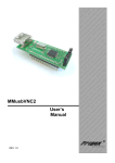
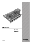
MMstm32F103R
MMstm32F103R
User’s
Manual
REV 1.1
u rd ST, ta- rve
l
a oa ,
S e
Ev B VR ers b S d
l
n
io 1, A trol We mo
t
i
a ‘5
in ron ed
r
c
fo cro dd s M the
e
s
d e
i
m mb oar rs, peC E B e S
PI its ng roll gh r
i
i
t
r K typ on H s fo
e
rt to roc FID er s
o c
r
Pr mi s, R mm lle
a
s
o
r or ler gr
tr
f ol
n
o
pr oco CB
es nt r
l
P r
u o
r
c tem ic s,
fo
t
m
s
s
m
e
d
e
n Sy T
st oar lS
n
y
I
,
s B
ro
ed PIC or ion ont b
s
,
c e
R ce luat cro W
V
A pro va mi ed iro E
dd
ic ng PIC be ds m
M ni T, m
r
g S E oa rs,
i
s
, ts
e
B
de VR Ki ng roll
h
t
i
r
, A rte typ on Hig
1
‘5 Sta oto roc ID c
r
e
rs P mi RF m
e
s
l
,
r
er fo ers ram trlv
g n
r
s
ll
Se ule tro pro oco
od con ms icr s,
m
ni net ste T m stem
er Sy , S sy Boh
et d In PIC sor on i
c
ee R, oce uat mi
p
l
S AV opr va IC e
r r
fo ic g E T, P mb
E
rs s M nin , S
s ing
r ig
t
R
i
e
l
ol des , AV er K typ
B `51 tart roto roC
S s P mic ,
P for
s
s ller er for lers
d
l
ar tro erw les tro S
n
u on am
o b
d
r
c
c
o
ro We im et rog o
n
n
p
ed Mi her m roc
d
d ds et ste ic
ar rs, Sy T m r
o
B olle In , S so
e
r
d
nt ee PIC roc sig
o
c Sp R, op De
h AV icr B Rion
g
t
i
H for rs M , PC lua
s oneasolution
e Many ideas
s
er roll em Ev ds
m nt
g ar
st
co Sy nin Bo
CONTENTS
1. Introduction....................................................................................................................................... 3
Features .................................................................................................................................................. 3
2. The Module ........................................................................................................................................ 4
Block Diagram ..................................................................................................................................... 4
Terminals Layout ............................................................................................................................... 5
STM32F103Rx Microcontroller ................................................................................................... 6
Serial Flash Memory ......................................................................................................................... 7
RESET circuit ....................................................................................................................................... 8
Voltage Regulator .............................................................................................................................. 8
USB D+ Pull-Up Circuit .................................................................................................................... 9
JTAG Connection ............................................................................................................................... 9
3. Evaluation Board .......................................................................................................................... 10
4. Specifications ................................................................................................................................ 11
5. Technical Assistance ................................................................................................................ 11
6. Guarantee......................................................................................................................................... 11
7. Assembly Drawings..................................................................................................................... 12
8. Dimensions ...................................................................................................................................... 13
9. Schematic ........................................................................................................................................ 13
2
1.
Introduction
MMstm32F103R is universal minimodule for the STM32 Cortex-3 microcontrollers from
STMicroelectronics. This microcontroller is available in the TQFP64 case which is
difficult to apply to prototype and amateur circuits due to the compactness of pins. We
have undertaken an attempt at placing it on a board of 40,5x35,5mm with a layout of
leads which matches the commonly available prototype circuit boards. In addition, we
have included 3.3V voltage regulator, a Serial Flash memory with a capacity of up to
8MB, a circuit monitoring the supply voltage and clock generator for microcontroller. All
ports and signals of the microcontroller are lead out by means of two-row pin
connectors with 0.1’ pitch. This minimodule is not only an adapter but a complete main
board for STM32F103Rx. It needs only a connection to the supply voltage and to the
JTAG connector and we can start loading 128kBytes of Flash memory of the
microcontroller.
Through integration of the peripherals with the microcontrollers on one board, the
application of this module can lead to a shorter design period and facilitate the
construction of systems based on ARM microcontrollers, by eliminating the need to
design the printed board. The module is supplied with example software.
The MMstm32F103R minimodule can be also used in didactic laboratories of
informatics colleges and universities, and can be also used to build circuits realizing
thesis projects.
Features
MMstm32F103R minimodule:
Complete, ready to use microprocessor system
Fast ARM Cotex-3 microcontroller STM32F103Rx with up to 90 DMIPS throughput
Serial Flash memory 64Mb (8MB)
Reliable reset circuit
Built-in system generator 8MHz
Built-in 32.768kHz crystal resonator for RTC
Built-in voltage regulator 3.3V 400mA
Module supply voltage: 3.3V or 3.8 - 9V
2 x 32 terminals with 0.1" (2.54mm) pitch fitting every prototype board
Small dimensions: 40.5mm x 35.5mm
Available evaluation board and sample applications
3
2.
The Module
Block Diagram
A block diagram of MMstm32F103R minimodule is shown on the image below:
Figure 1 Block diagram of MMstm32F103R
Minimodule can be ordered in different configurations with use of selector:
MMstm32F103R – f – d – b
Flash memory size:
0 – 32kB
1 – 64kB
2 – 128kB
Serial Flash memory size:
0 – not mounted
1 – 8MB
Battery holder:
0 – not mounted
1 – mounted
4
Terminals Layout
Figure 2 Terminals Layout – top view
J1
J2
1
Main
Function
PA9
2
PA8
3
PA11
4
5
PA10
USART1_TX/TIM1_CH2
USART1_CK/
TIM1_CH1/MCO
USART1_CTS / CANRX
TIM1_CH4 / USBDM
USART1_RX/TIM1_CH3
JTMS/SWDIO
PA13
6
PA12
USART1_RTS / CANTX
TIM1_ETR / USBDP
7
8
9
JTDI
JTCK/SWCLK
PA15
PA14
PC11
7
8
9
10
PC10
10
PB14
11
PD2
11
PB13
12
PC12
12
PB12
13
14
15
NTRST
JTDO
13
14
15
PB11
PB10
PB2/BOOT1
Pin
PB6
Alternate Function
Pin
1
Main
Function
VCC
2
GND
3
3.3V
4
5
GND
PC9
6
PC8
PC7
PC6
PB15
TIM3_ETR
PB4
PB3/TRACESWO
I2C1_SCL / TIM4_CH1
Alternate Function
SPI2_MOSI / TIM1_CH3N
SPI2_MISO/USART3_RTS
TIM1_CH2N
SPI2_SCK/
USART3_CTS/TIM1_CH1N
SPI2_NSS /I2C2_SMBAl/
USART3_CK/TIM1_BKIN
I2C2_SDA / USART3_RX
I2C2_SCL / USART3_TX
5
16
17
18
19
PB5
BOOT0
UDP_PUP
PB7
I2C1_SDA / TIM4_CH2
16
17
18
19
PB1
PB0
PC5
PC4
20
PB8
TIM4_CH3
20
PA7
21
PB9
TIM4_CH4
21
PA6
22
VBAT
22
PA5
23
PC2
ADC_IN12
23
PA4
24
PC1
ADC_IN11
24
PA3
25
PC0
ADC_IN10
25
PA2
26
PC13
ANTI_TAMP
26
PA1
27
#NRST
27
PA0
28
29
30
31
32
NC
NC
NC
NC
NC
28
29
30
31
32
PC3
PA4-DF_CS
PA6-DF_Q
PA5-DF_C
PA7-DF_D
I2C1_SMBAl
ADC_IN9 / TIM3_CH4
ADC_IN8 / TIM3_CH3
ADC_IN15
ADC_IN14
SPI1_MOSI/
ADC_IN7 / TIM3_CH2
SPI1_MISO/
ADC_IN6 / TIM3_CH1
SPI1_SCK / ADC_IN5
SPI1_NSS/
USART2_CK / ADC_IN4
USART2_RX/
ADC_IN3 / TIM2_CH4
USART2_TX/
ADC_IN2 / TIM2_CH3
USART2_RTS/
ADC_IN1 / TIM2_CH2
WKUP/USART2_CTS/AD
C_IN0 / TIM2_CH1_ETR
ADC_IN13
STM32F103Rx Microcontroller
32-bit Cortex-M3 core
72 MHz, 90 DMIPS with 1.25 DMIPS/MHz
From 32 to 128kB in system programmable flash memory
From 10 to 20kB SRAM memory
Up to three 16-bit timers, each with up to 44 UART interfaces IC/OC/PWM or pulse
counter
16-bit, 6-channel advanced control timer
2 x 16-bit watchdog timers
Up to 2 x I2C interfaces (SMBus/PMBus)
2 SPI interfaces
Up to 3 USARTs (ISO 7816 interface, LIN, IrDA capability, modem control)
Up to 2 SPIs (18 Mbit/s)
USB 2.0 full speed interface
CAN interface (2.0B Active)
RTC clock
2 x 12-bit, 1 us A/D converters (16-channel)
49 5 V-tolerant I/Os
Nested interrupt controller with 43 maskable interrupt channels
Sleep, Stop and Standby modes
4-to-16 MHz quartz oscillator
Internal 8 MHz factory-trimmed RC
Internal 32 kHz RC
PLL for CPU clock
2.0 to 3.6V application supply
Serial wire debug (SWD) & JTAG interfaces
6
Serial Flash Memory
The minimodule can be equipped with Serial Flash memory M25P64 (8MB capacities). The
memory is connected to a fast SPI bus with up to 18MBit/s transmission speed.
Figure 3 Serial Flash memory connection
Memory is available directly on minimodule pins:
PA4 – DF_CS
PA5 – DF_C
PA6 – DF_Q
PA7 – DF_D
Chip Select
Clock Input
Data Output
Data Input
It is also connect to microcontroller ports by 0Ω resistors and it can by directly use without
outside connections.
It should be kept in mind that if Serial Flash memory is installed, the just outlined port terminals
cannot be used externally to the module. Of course the SPI bus can be used for
communication with external peripherals, under the condition that they will have circuit
selection inputs (CS).
A detailed description of Serial Flash circuits is on the STMicroelectronics page: www.st.com.
7
RESET circuit
The MMstm32F103R has a built-in voltage monitoring circuit built around the DS1818
integrated circuit. The circuit generates a RESET signal in case when the supply voltage value
is lower than 3V. This takes place when the supply voltage is switched on or off, when the
VCC voltage changes its value from 0 to 3.3 V. The guard circuit detects also momentary VCC
voltage drops. A short duration drop of VCC below 3V causes the generation of a resetting
signal of 100 ms duration. This signal is applied directly to the resetting input of the
microcontroller and is led out to a module connector and it can be used as the zeroing output
resetting external circuits and as the input for resetting the module, e.g. by means of the
RESET button. In such a case the RESET button can short the RESET line directly to ground.
An implementation of the reset circuit is presented in the diagram below.
Figure 4 RESET circuit implementation
Voltage Regulator
Minimodule has built-in 3.3V voltage regulator. Thanks to it can be powered with 3.3V voltage
supplied to J2 3 pin (+3.3V) or with voltage between 3.8 – 9V, supplied to J2 1 pin (VCC).
When power is supplied to VCC pin, then 3.3V voltage is produced on the module by U3
regulator. In this case 3.3V voltage can be also used outside the module, if current draw will
not exceed 300mA.
Figure 5 3.3V Voltage Regulator
8
USB D+ PullPull-Up Circuit
USB host recognize presence of device on the bus by sensing pull-up on D+ line.
MMstm32F103R has built-in pull-up circuit, shown on drawing below.
Figure 6 USB D+ Pull-Up circuit implementation
Pull-up is by default turned off by R7 resistor. Active reset signal or low level on UDP_PUP
(R16 mounted) line turns on pull-up, what is interpreted by USB host as connection of USB
device.
JTAG Connection
JTAG is a four-lead interface permitting the takeover of control over the processor’s core. The
possibilities offered by this interface are, among others: step operation, full-speed operation,
hardware and software breakpoints, inspection and modification of contents of registers and
data memories. The method of connecting the JTAG connector to the minimodule is shown in
the drawing:
Figure 7 JTAG connection on module
9
JTAG programmer/debugger may be found on page:
ARM cable I http://www.propox.com/products/t_122.html
3.
Evaluation Board
EVBmm™
10
4.
Specifications
Microcontroller
STM32F103Rx
Program Memory
up to 128kB
SRAM Memory
up to 20kB
Serial Flash Memory
8MB
Digital in/out
up to 49
Analog inputs
up to 15
Power Supply
3.3V or 3.8 – 9V
Dimensions
40,5x35,5mm
Weight
about 80g
Temperature range
0 – 70ºC
Connectors
Two gold-pin connectors - 2x32
5.
Technical Assistance
In order to obtain technical assistance please contact [email protected] . In the request
please include the following information:
•
6.
a detailed description of the problem
Guarantee
The MMstm32F103R minimodule is covered by a six-month guarantee. All faults and defects
not caused by the user will be removed at the Producer’s cost. Transportation costs are borne
by the buyer.
The Producer takes no responsibility for any damage and defects caused in the course of
using the MMstm32F103R module.
11
7.
Assembly Drawings
Figure 8 TOP
Figure 9 Bottom
12
8.
Dimensions
Figure 10 Top View
Figure 11 Side View
9.
Schematic
13
14