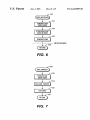
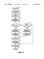
1
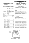
US006243809B1
(12) United States Patent
(10) Patent No.:
(45) Date of Patent:
Gibbons et al.
(54)
METHOD OF FLASH PROGRAMMING OR
READING A ROM OF A COMPUTER
SYSTEM INDEPENDENTLY OF ITS
OPERATING SYSTEM
(75) Inventors: Patrick L. Gibbons, Magnolia; Paul J.
Broyles, III, Cypress, both of TX (US)
(73) Assignee: Compaq Computer Corporation,
US 6,243,809 B1
Jun. 5, 2001
Intel Corporation, Intel486TM SL Microprocessor SuperSet
Programmer’s Reference Manual, System and PoWer Man
agement, pp. 6—28 through 6—53.
Intel Corporation, PentiumTM Processor User’s Manual, vol.
3: Architecture and Programming Manual, @ Intel Corpo
ration 1994, pp. 20—1 through 20—9.
* cited by examiner
Primary Examiner—Robert Beausoleil
Assistant Examiner—Rita Ziemer
Houston, TX (US)
(74) Attorney, Agent, or Firm—Akin, Gump, Strauss,
(*)
Notice:
Subject to any disclaimer, the term of this
patent is extended or adjusted under 35
U.S.C. 154(b) by 0 days.
Hauer & Feld, LLP
(57)
ABSTRACT
A computer system provides for ?ashing a non-volatile
(21) Appl. No.: 09/070,823
(22) Filed:
Apr. 30, 1998
(51)
(52)
(58)
Int. Cl.7 ...................................................... .. G06F 9/00
US. Cl. ............................................... .. 713/1; 713/100
Field of Search ........................................ .. 713/1, 100
(56)
U.S. PATENT DOCUMENTS
8/1994 Yuen .................................. .. 395/700
5,375,243 * 12/1994 ParZych eta.
5,684,997
*
5,724,027
11/1997
Kau et al.
......
3/1998 Shipman et al.
710/200
. . . . . ..
710/260
340/825.31
5,724,544 *
3/1998
5,796,984 *
8/1998 Pearce et al. ..
713/1
5,809,515 * 9/1998 Kaki etal.
5,835,594 * 11/1998 Albrecht et a1.
711/103
380/23
5,835,760 * 10/1998
Nishi ............ ..
711/115
Harmer ........ ..
713/2
5,859,911 *
1/1999 Angelo et a1. ....................... .. 380/25
5,898,843 *
5,956,743 *
4/1999
9/1999
Deceased et a1. ................... .. 360/39
Bruce et al. ..... ..
711/103
5,963,738 * 10/1999 Yamaki et al.
6,009,520
*
12/1999
6,009,524 * 12/1999
Gharda
.. ... ... ...
image to the non-volatile memory is desired, the image
buffer is loaded With a portion of the non-volatile memory
image. BIOS interface code is then called to place an SMI
event code into a memory and to generate a system man
References Cited
5,339,437
memory image to a non-volatile memory and reading data
from a non-volatile memory independently of an operating
system. An image buffer is allocated in a volatile memory of
the computer system. If ?ashing a non-volatile memory
713/100
. . . . . . ..
agement interrupt causing the computer system to enter a
system management mode. SMI handler code examines the
SMI event code and calls SMI service code. Next, the image
buffer is located and the portion of the non-volatile memory
in the image buffer is ?ashed to the non-volatile memory by
the SMI service code. Locating the image buffer may
include locating an image header de?ned Within the volatile
memory. The image header may include a passWord for
providing access to the non-volatile memory. The steps of
loading the image buffer, calling BIOS interface code, and
?ashing a portion of the non-volatile memory image to the
non-volatile memory may be repeated until the entire non
volatile memory image is ?ashed to the non-volatile
memory. Alternatively, if reading data from a non-volatile
memory independently of an operating system is desired, a
system management interrupt is generated to place the
713/1
Olarig et al. ....................... .. 713/200
OTHER PUBLICATIONS
Advanced Micro Devices, Inc., “Am291F002T/
Am29F002B, 2 Megabit (262,144><8—Bit) CMOS 5.0 Vol
t—only, Sector Architecture, Flash Memory,”@ 1996, pp.
computer system in a system management mode, an SMI
event code is placed in a memory, the SMI handler code
processes the SMI event code and calls SMI service code,
the image buffer is located by the SMI service code, and the
SMI service code copies data from the non-volatile memory
to the image buffer.
29 Claims, 9 Drawing Sheets
1—34.
SUlM/IEEHEADER
cum/mu Inn/1587mm
an HASH w
wnunrss an
U.S. Patent
Jun. 5, 2001
Sheet 2 0f 9
Q»\Eg?m
\av\
x35%mm
Q56:2::2
52
k
8
mmf
\
8
_
\
B\x85;.*8vain
.8\22m8E3
\2 :8
E.85
252a:
[mmE\Eéamm\22(2
2.,828k%
mmvm\
\Q:5%Cam
Eg
:S@2a53:m
US 6,243,809 B1
U.S. Patent
Jun. 5, 2001
Sheet 3 0f 9
US 6,243,809 B1
72
FLA
AP
RIVER!
ATIDN
74
FLAS
TE
(
0S
CE
_INTERFACE)
76
BIOS snvn
HAN
nu
_HANDLER)
78
BIDS SMI
SERVICE
nuunma
(SMI__SERVICE)
FIG. 3A
IMAGE
CMDS
HEADER
U.S. Patent
Jun. 5, 2001
Sheet 4 0f 9
100
( RDM_FLASH )
[102
ALLDCATE IMAGE
BUFFER & IMAGE
HEADER
INITIALIZE IMAGE
HEADER ID
‘
0/105
SET
IMAGE_BUFFER_ADDRESS
SET
IMAGE__LENGTH TU n
SET
IMAGE_UFFSET T0 0
,-110
SET IMAGE HEADER
CDMMAND T0 FLASH_CMD
II
,-112
FILL IMAGE BUFFER WITH
n BYTES 0F ROM IMAGE
CALCULATE HASH DF
IMAGE BUFFER AND
PLACE IN MESSAGE
DIGEST FIELDS
v
SET FLASH IN
PROGRESS BIT
CALL BIDS INTERFACE
TD FLASH IMAGE
FIG. 4A
/'115
US 6,243,809 B1
U.S. Patent
Jun. 5, 2001
Sheet 5 0f 9
US 6,243,809 B1
r117
CLEAR FLASH IN
PROGRESS BIT
K120
ADD nTO
IMAGE_0FFSET
122
'IMAGE_D FFSET
=TOTAL ROM
IMAGE SIZE
U.S. Patent
Jun. 5, 2001
Sheet 6 0f 9
US 6,243,809 B1
126
ROM_READ
r128
ALLDCATE IMAGE
BUFFER & IMAGE
HEADER
r130
INITIALIZE IMAGE
HEADER ID
f132
SET
IMAGE_LENGTH TD n
,134
SET
IMAGE_DFFSET TD 0
,136
SET IMAGE HEADER
COMMAND T0
BACKUP_CMD
l
CALL BIDS INTERFACE
TD READ RDM DATA
FIG. 5A
r 138
U.S. Patent
Jun. 5, 2001
Sheet 7 0f 9
i
US 6,243,809 B1
r 142
PROCESS IMAGE BUFFERI
r144
ADD n TU
|MAGE__0FFSET
146
IMAGE_0FFSET
TOTAL DZXTA SIZE
ROM_READ
COMPLETE
FIG. 5B
U.S. Patent
Jun. 5, 2001
Sheet 8 0f 9
150
‘ BIUSJNTERFACE )
r152
GENERATE SMI
EVENT CODE
‘
f 154
STORE SMI EVENT
CODE IN CMUS
GENERATE SMI
_____________ -- ENTER SMI MUDE
"
158
RETURN
FIG. 6
160
SM|_HANDLER
162
PROCESS SM!
EVENT CODE
CALL SMl_v SERVICEf‘I
EXIT SMM
( RETURN )
FIG. 7
US 6,243,809 B1
U.S. Patent
Jun. 5, 2001
Sheet 9 0f 9
US 6,243,809 B1
168
I SMI_SERVICE )
M
f 170
LOCATE AND READ
IMAGE HEADER
"
f‘
VERIFY MESSAGE
DIGEST
PROVIDE
PASSWORD TO
ENTER ADMIN MODE
192
COMMAND
COMMAND CUBE =
CUBE =
FLASHTCMD
BACKUP_CMD
-
?
YES
/ 176
ENABLE FLASH
PROGRAMMING
ENABLE FLASH
PROGRAMMING
FLASH IMAGE
"
TO f
FLASH RDM
READ DATA
v FROMf‘
FLASH RDM
;
l
v
r 182
VERIFY RESULT
DISABLE FLASH
PROGRAMMING
;
r186
EXIT ADMIN MDDE
I
r 194
190
( RETURN )
FIG. 8
US 6,243,809 B1
1
2
METHOD OF FLASH PROGRAMMING OR
READING A ROM OF A COMPUTER
SYSTEM INDEPENDENTLY OF ITS
OPERATING SYSTEM
SUMMARY OF THE INVENTION
Brie?y, the present invention provides a method of ?ash
ing a non-volatile memory image to a non-volatile memory
of a computer system and reading data from a non-volatile
memory independently of an operating system. An image
BACKGROUND OF THE INVENTION
1. Field of the Invention
The present invention relates to ?ashing and reading a
non-volatile memory, and more particularly to ?ashing and
reading a read-only memory of a computer system indepen
buffer is allocated in a volatile memory of the computer
system. If ?ashing a non-volatile memory image to the
non-volatile memory is desired, the image buffer is loaded
With a portion of the non-volatile memory image. BIOS
10
dently of its operating system.
causing the computer system to enter a system management
mode.
In the system management mode, an SMI handler code
2. Description of the Related Art
Access to ?ash ROM devices in a computer system is
increasingly being safeguarded by softWare and/or hardWare
protection and virtualiZation mechanisms. Such
mechanisms, Which range from block locking and Write
protection to passWord protection and secure memory
devices, may be traversed by devices having the necessary
privilege level. In a computer system, an application is
15
examines the SMI event code and calls SMI service code.
Next, the SMI service code locates the image buffer, and the
portion of the non-volatile memory in the image buffer is
?ashed to the non-volatile memory. Locating the image
buffer may include locating an image header de?ned Within
the volatile memory. The image header may include a
passWord for providing access to the non-volatile memory.
typically given the loWest privilege level. An application
The steps of loading the image buffer, calling BIOS interface
requiring direct access to a ?ash ROM device, such as
code, and ?ashing a portion of the non-volatile memory
image to the non-volatile memory may be repeated until the
softWare for ?ashing a ROM image or for reading a version
of a ROM, thus must be able to direct a device having the
necessary privilege level to release security protection for
interface code is then called to place an SMI event code into
a memory and to generate a system management interrupt
25
the ?ash ROM device. Similarly, access to certain areas of
a memory space of a computer system, such as high regions
entire non-volatile memory image is ?ashed to the non
volatile memory. Alternatively, if reading data from a non
volatile memory independently of an operating system is
SoftWare for ?ashing a ROM image or for reading a
version of a ROM has traditionally relied upon a driver to
desired, a system management interrupt is generated to place
the computer system in a system management mode, the
image buffer is located, and data from the non-volatile
memory is copied to the image buffer.
The present invention further provides a method of pro
obtain a privilege level necessary to release any security
viding a memory command to a non-volatile memory having
protection for a ?ash ROM device and to access certain areas
a locked state independently of the operating system. The
computer system is placed in a system management mode,
of memory Where critical code is often stored, has required
a particular privilege level.
of a memory space. Drivers (also called device drivers),
Which generally serve to link a peripheral device to an 35 and an SMI event code is placed into a memory. The SMI
operating system, are commonly used in programming and
handler code processes the SMI event code and calls the
reading ?ash ROM devices in a computer system. In
particular, a driver is typically used to control command and
status registers of a ?ash ROM device for erasing, Writing,
or reading the device. Various types of information may be
SMI service code. Next, an image buffer and image header
are located in a volatile memory of the computer system.
The image header is then read, and a passWord is provided
from the image header to a secure memory device. If the
read from a ?ash ROM device, such as status data, ROM
version data, device identi?cation data, or a ROM image.
Accessing a ?ash ROM device to read or Write data has
passWord provided matches the passWord stored in the
secure memory device, the secure memory device places the
non-volatile memory in an unlocked or unprotected state. A
occurred exclusively in an operating system environment.
Accessing a ?ash ROM device in an operating system
protected command may then be provided from the image
45
header to the non-volatile memory by the SMI service code.
environment, hoWever, has required updates to drivers for
The non-volatile memory or a volatile memory of the
each hardWare and operating system environment in Which
computer system stores a driver for performing the method
of ?ashing a non-volatile memory image to the non-volatile
memory and reading from a non-volatile memory indepen
dent of an operating system. The BIOS interface code, SMI
handler code, and SMI service code are also stored in the
access to a ?ash ROM device is desired. Such updates, for
example, may account for de?nitions of neW bus interface
standards and neW memory standards. Drivers are also
frequently updated to handle neW ROM versions of appli
cation softWare, neW device identi?cation codes, or neW
non-volatile memory or a volatile memory. In a system
memory siZe boundaries. It has been necessary, therefore, to
match maintenance of a driver for accessing a ?ash ROM
management mode, the SMI service code operates at a high
privilege level Which gives the SMI service code access to
the non-volatile memory and the full memory space of the
computer system. In accordance With the present invention,
reading or ?ashing non-volatile memory thus is not depen
device With the frequency of changes in the hardWare
environment of the ?ash ROM device, the operating system
environment, and ROM versions.
Most of today’s computer systems provide an operating
55
dent upon the operating system.
state knoWn as a protected mode Which supports advanced
BRIEF DESCRIPTION OF THE DRAWINGS
features. A protected mode has provided hardWare support
for multitasking and virtual memory management. At certain
times in a protected mode, hoWever, an operating system has
been unable to grant a driver the privilege level necessary to
release security protection for a ?ash ROM device. An
application thus has not been guaranteed access to a ?ash
ROM device When a computer system is in a protected
mode.
A better understanding of the present invention can be
obtained When the folloWing detailed description of the
preferred embodiment is considered in conjunction With the
folloWing draWings, in Which:
65
FIG. 1 is a schematic diagram of a computer system
incorporating ?ash ROM security features in accordance
With the present invention;
US 6,243,809 B1
4
3
management, suspend and resume logic, advanced con?gu
ration and poWer interface (ACPI), and system management
FIG. 2 is a schematic diagram of a Super I/O chip and a
security chip for ?ash ROM security management in accor
dance With the present invention;
bus (SMBus) control, Which implement the inter-integrated
circuit (I2C) control. The ISA bridge 24 supports standard
FIG. 3A is a control ?oW diagram of a ROM ?ashing and
personal computer input/output (I/O) functions, including a
dynamic memory access (DMA) controller, interrupt
reading process in accordance With the present invention;
FIG. 3B is a data ?oW diagram of the ROM ?ashing and
reading process of FIG. 3A;
FIGS. 4A and 4B are ?oW charts of an exemplary ROMi
FLASH routine in accordance With the present invention;
10
FIGS. 5A and 5B are ?oW charts of an exemplary ROMi
netWork interface controller (NIC) 22. The NIC 22 prefer
ably supports the THUNDERLANTM poWer management
READ routine in accordance With the present invention;
speci?cation by Texas Instruments.
FIG. 6 is a ?oW chart of an exemplary BIOSi
INTERFACE routine in accordance With the present inven
tion;
15
FIG. 7 is a ?oW chart of an exemplary SMIiHANDLER
The ISA bus 25 couples the ISA bridge 24 to a Super I/O
chip 32, Which in the disclosed embodiment is a National
Semiconductor Corporation PC87307VUL device. This
Super I/O chip 32 provides a variety of input/output
routine in accordance With the present invention; and
functionality, including a disk drive controller for a disk
drive 36, serial ports 38, a mouse port for a mouse 40, a
FIG. 8 is a ?oW chart of an exemplary SMIiSERVICE
routine called by the SMIiHANDLER routine of FIG. 7 in
accordance With the present invention.
controllers, a timer, and a real time clock (RTC).
The PCI bus 21 couples a variety of devices that generally
take advantage of a high speed data path. This includes a
small computer system interface (SCSI) controller 20 and a
20
keyboard controller for a keyboard 42, a parallel port 46, and
an IrDA port 44. These devices are coupled through con
nectors to the Super I/O chip 32. The Super I/O chip 32
DETAILED DESCRIPTION OF THE
PREFERRED EMBODIMENT
The folloWing patent applications are hereby incorporated
by reference as if set forth in their entirety:
preferably includes a battery-backed memory 34 such as a
25
The ISA bus 25 is further coupled to a system ROM 30
Common-assigned US. patent application Ser. No.
(FIGS. 2 and 3) implemented as ?ash read-only memory.
08/396,343, entitled “SECURITY CONTROL FOR
PERSONAL COMPUTER,” ?led on Mar. 3,1995;
Commonly-assigned US. patent application Ser. No.
30
09/070,458, entitled “METHOD AND APPARATUS
The system ROM 30 includes basic input/output services
(BIOS) code for execution by the processor 12. The ISA bus
25 couples the ISA bridge 24 to a security, poWer, ACPI, and
miscellaneous application speci?c integrated circuit (ASIC)
FOR PROVIDING REMOTE ACCESS TO SECU
RITY FEATURES ON A COMPUTER NETWORK,”
48, Which provides a variety of miscellaneous functions for
the computer system S. The ASIC 48 includes security
?led on Apr. 30, 1998,
Commonly assigned US. patent application Ser. No.
CMOS memory for storage of passWords supported by the
computer system S.
features, system poWer control, light emitting diode (LED)
09/070,866, entitled “METHOD AND APPARATUS
control, a PCI arbiter, remote Wakeup logic, system fan
control, hood lock control, ACPI registers and support,
FOR FLASHING ESCD AND VARIABLES INTO A
system temperature control, and various glue logic.
35
ROM,” ?led on Apr. 30, 1998; and
Referring to FIG. 2, the contents of the Super I/O chip 32
Commonly assigned US. patent application Ser. No.
09/,070,942, entitled “METHOD AND APPARATUS
and security ASIC 48 for use With the present invention are
40
FOR REMOTE ROM FLASHING AND SECURITY
MANAGEMENT FOR A COMPUTER SYSTEM,”
?led on Apr. 30, 1998.
Turning to FIG. 1, illustrated as a typical computer system
S implemented according to the present invention. While
this system is illustrative of one embodiment, the techniques
according to the present invention can be implemented in a
Wide variety of systems. The computer system S in the
illustrated embodiment is a PCI bus/ISA bus based machine,
45
having a peripheral component interconnect (PCI) bus 21
and an industry standard architecture (ISA) bus 25. The PCI
bus 21 is controlled by PCI controller circuitry Within a host
bridge 18. The host bridge 18 couples the PCI bus 21 to a
host bus 15. The disclosed host bridge 18 includes interface
circuitry for a system random access memory (RAM) 16.
The system RAM 16 preferably supports extended data out
55
(EDO), dynamic random access memory (DRAM) and
synchronous DRAM (SRAM). An ISA bridge 24 bridge is
60
microprocessor core 12 and a level 2 (L2) cache 14.
The ISA bridge 24 includes an integrated IDE controller
for controlling up to four enhanced IDE drives 28 and a
universal serial bus (USB) controller for controlling USB
ports 26. The ISA bridge 24 also includes enhanced poWer
management. The enhanced poWer management Within the
ISA bridge 24 includes full clock control, device
passWord. The ?ash ROM passWord controls access to the
system ROM 30. CMOS memory 34 may also include a
CMOS location 51 for storing a user poWer-on passWord and
a CMOS location 53 for storing an administrator passWord.
In the disclosed embodiment, the ?ash ROM passWord is the
administrator passWord. Access to the CMOS locations 50,
51 and 53 is controlled by an AEN signal 68 externally
designated as SIOAEN 64, and an IOWC# signal 70 exter
nally designated as SIOWCL 66. It should be understood
that components Within the Super I/O chip 32 Which are not
related to the present invention have been omitted.
The security ASIC 48 includes a “black box” 52. The
black box 52, Which is a secure memory device for locking
and unlocking resources Within the computer system S such
as the system ROM 30, is coupled to a black box status/data
register 60 and a black box command register 58. In the
disclosed embodiment, the black box 52 provides three
slots: Slot 0, Slot 1, and Slot 2, respectively. Slot 0 indicated
betWeen the PCI bus 21 and the ISA bridge 25. The host bus
15 is coupled to a processor module 10 Which includes a
shoWn. The CMOS memory 34 Within the Super I/O chip 32
includes a CMOS location 50 for storing a ?ash ROM
at 49 is used to store the ?ash ROM passWord for locking
and unlocking the system ROM 30. When the system ROM
30 is in a locked state, Write cycles to the system ROM 30
are blocked. When the system ROM 30 is in an unlocked
65
state, Write cycles and read cycles to the system ROM 30 are
permitted. Slot 1 indicated at 54 may be used for storing the
user poWer-on passWord, and Slot 2 indicated at 56 may be
used for storing the administrator passWord.
US 6,243,809 B1
5
6
In the disclosed embodiment, the blackbox command
register 58 is a 7-bit I/O mapped register. Bits 7—5 are index
bits allowing for selection of a particular slot of the black
box 52. A command provided to the blackbox command
register 58 is directed to the particular slot selected. Bit 4 is
66. If the security logic 62 asserts the SIOAEN signal 64,
blockage of Write operations to the passWord CMOS loca
preferably reserved and therefore should return a “0” When
read. Bits 3—0 are used for storing a blackbox command
provided to the blackbox command register 58. The com
mand sequence ’0000’ represents a Read Status blackbox
command. The Read Status blackbox command causes the
tions 50, 51 and 53 occurs. If the security logic 62 asserts the
SIOWCL signal 66, both Writes and reads are blocked to the
passWord CMOS locations 50, 51 and 53. If both the
SIOAEN signal and the SIOWCL signal 66 are deasserted,
read and Write cycles to the passWord CMOS locations 50,
51 and 53 may be decoded. BIOS code in connection With
the security chip 48 and the Super I/O chip 32 thus controls
10
the status of the black box 52. The command sequence
’0001’ represents the Store PassWord blackbox command.
FolloWing the Store PassWord blackbox command, the next
8 bytes Written to the blackbox status/data register 60 are
access to the ?ash ROM passWord used for locking and
unlocking the system ROM 30.
next byte read from the blackbox status/data register 60 to be
Referring to FIG. 3A, a control ?oW diagram of a process
15
for ?ashing and reading the system ROM 30 in accordance
With the present invention is shoWn. Referring to FIG. 3B,
a data ?oW diagram of the process for ?ashing and reading
the system ROM 30 is shoWn. The solid-line arroWs
stored as the passWord. The command sequence ’0010’
represents the Protect Resources blackbox command. The
Protect Resources blackbox command locks a selected
blackbox slot. The command sequences ’0100’ represents
the Access Resources blackbox command. The Access
Resources blackbox command compares the next 8 bytes
Written to the status/data blackbox register 60 With the
components in FIG. 3A represent softWare for the disclosed
embodiment, and the components in FIG. 3B represent
hardWare for the disclosed embodiment. In accordance With
the present invention, at boot up of the computer system S,
passWord bytes previously stored in the selected blackbox
the system ROM 30 includes in its contents a ?ash driver or
slot using the Store PassWord blackbox command. If each
byte is the same, then the Access Resources command
unlocks the selected blackbox slot. The command sequence
’1000’ represents the Permanently Locked Resource black
box command. The Permanently Locked Resource blackbox
command prohibits access to the selected blackbox slot until
depicted represent control ?oW (FIG. 3A), and the phantom
line arroWs depicted represent data ?oW (FIG. 3B). The
25
During runtime, the system RAM 16 includes the ?ash
driver 72, a ?ash BIOS interface 74, the BIOS SMI handler
routine 76, and the BIOS SMI service routine 78. It should
be understood that the ?ash driver 72, the ?ash BIOS
interface 74, the BIOS SMI handler routine 76, and the
BIOS SMI service routine 78 may be contained in a volatile
the security ASIC 48 is reset. Blackbox commands are
provided to the blackbox command register 58 by BIOS
code.
memory, non-volatile memory or any medium suitable for
storing code to be executed by a processor.
Further, in the disclosed embodiment, the blackbox status/
data register 60 is an 8-bit I/O mapped register. For a Write
operation, bits 7—0 represent the passWord byte, While the
The ?ash driver 72 allocates an image buffer 80 and an
35
command using the image buffer 80. The ?ash driver 72 next
calls the ?ash BIOS interface 74. The ?ash BIOS interface
74 places an SMI event code into the CMOS memory 34 and
then generates a system management interrupt (SMI). The
SMI causes the processor 12 to place the computer system
S in a system management mode (SMM). Entering SMM
45
in progress occurs When there is a passWord mismatch. If
there is a passWord match, there is no delay in progress. In
the disclosed embodiment, a ’1’ refers to a delay in progress,
and a ’0’ refers to the absence of a delay in progress.
The 0 bit indicates Whether the selected slot is protected
or unprotected. If a ’1’ is stored in the 0 bit, the selected slot
is protected, and if a ’0’ is stored in bit 0, the selected slot
is unprotected. Further details concerning the operation of
the black box 52, the blackbox command register 58, and the
blackbox status/data register 60 are provided in commonly
assigned US. patent application Ser. No. 08/396,343,
55
entitled “SECURITY CONTROL FOR PERSONAL
previously incorporated by reference. It should be under
stood that the number of bits and bytes in the particular bit
The security ASIC 48 also includes security logic 62 for
controlling the SIOAEN signal 64 and the SIOWCL signal
transfers control directly from the ?ash BIOS interface 74 to
the BIOS SMI handler routine 76. The SMI handler routine
76 examines the SMI event code in the CMOS memory 34.
The SMI event code directs the BIOS SMI handler 76 to call
the BIOS SMI service routine 78.
The BIOS SMI service routine 78 locates the image
header 82 and processes the information in the image header
82. If the ROM command is a ?ash command, the image
buffer 80 is ?lled With a portion of a ROM image to be
?ashed to the system ROM 30. The BIOS SMI service
routine 78 then executes the particular ROM command. For
a ?ash command, a ROM image is provided from the image
buffer 80 to the system ROM 30 as indicated by phantom
line arroW 81. For a read command, data is provided from
the system ROM 30 to the image buffer 80 as indicated by
phantom-line arroW 83. Flashing and reading the system
ROM 30 from SMM alloWs for ROM ?ashing and reading
independently of the runtime environment of the computer
COMPUTER,” and commonly-assigned US. patent appli
cation Ser. No. 9/070,458., entitled “METHOD AND APPA
RATUS FOR PROVIDING REMOTE ACCESS TO SECU
RITY FEATURES ON A COMPUTER NETWORK,”
sequences and register siZes as described may be varied to
achieve other embodiments of the black box 52.
image header 82 in the system RAM 16. The image header
82 contains a variety of information for performing a ROM
blackbox status/data register 60 serves as a data register for
a Write operation, the blackbox status/data register 60 serves
as a status register for a read operation. Referring to a read
operation, bits 7—5 represent index bits for selection of a
particular slot of the black box 52. Bits 4—3 are reserved and
therefore should return a ’0’ if read. Bit 2 indicates Whether
a selected slot is permanently locked. If a ’1’ is stored in bit
2, the selected slot is permanently locked, and if a ’0’ is
stored in bit 2, the selected slot is not permanently locked.
Bit 1 indicates Whether there is a delay in progress. A delay
application 72, a ?ash BIOS interface 74, a BIOS SMI
handler routine 76, and a BIOS SMI service routine 78.
65
system S. After the system ROM 30 is ?ashed or read, the
BIOS SMI routine 78 returns the processor 12 back to its
normal operating mode. This overall process may be
repeated a number of times in order to iteratively ?ash or
read the system ROM 30.
Referring to FIGS. 4A and 4B, an exemplary ROMi
FLASH routine 100 for executing a ROM ?ash process in
US 6,243,809 B1
7
8
accordance With the present invention is shown. The ROMi
FLASH routine 100 is performed in the ?ash driver 72 (FIG.
Where the command parameter is set to FLASHiCMD
representing a command to perform a ?ash operation. Next,
in step 112, the image buffer 80 is ?lled With n bytes of a
3A). Beginning at step 102, the image buffer 80 and the
image header 82 (FIG. 3B) are allocated in the system RAM
ROM image.
The ROM image may be resident to the computer system
16. In the disclosed embodiment, the image buffer 80 is a
physically contiguous memory area. The siZe of the image
S or may be delivered to the computer system S. Details
concerning remote and secure packaging and delivery of a
buffer 80 may be equal to or less than the siZe of a ROM
ROM image are provided in commonly-assigned US. patent
application Ser. No. 09/,070,942, “METHOD AND APPA
image to be ?ashed. The image header 82 contains several
?elds of data for use in performing a ?ash or read of the
system ROM 30. An exemplary structure for the image
10
header 82 is de?ned beloW:
RATUS FOR REMOTE ROM FLASHING AND SECU
RITY MANAGEMENT FOR A COMPUTER SYSTEM,”
previously incorporated by reference. It should be under
stood that the softWare of the present invention may be
struct imageiheader
unsigned
unsigned
unsigned
unsigned
unsigned
stored on a processor readable medium external to the
15
long headeriidilo;
long headeriidihi;
long imageibufferiaddress;
long imageioffset;
long imageilength;
system, it should be understood that the techniques accord
ing to the present invention may be implemented in other
systems Which also contain ?ash memory.
From step 112, control proceeds to step 114 Where a hash
of the image buffer 80 is calculated. The hash is placed in the
unsigned short command;
unsigned short result;
unsigned
unsigned
unsigned
unsigned
unsigned
unsigned
long passWordilo;
long passWordihi;
long msgidigestiO;
long msgidigestil;
long msgfdigestfZ;
long msgidigesti3;
computer system S and then delivered to a processor read
able medium internal to the computer system S. Wle the
present invention is illustrated in the context of a computer
message digest parameters, msLdigesti0, msgidigestil,
msgidigesti2, and msgidigestin3. In the disclosed
25
I‘;
The headeriidilo and headeriidihi ?elds or param
embodiment, the hash is a MD5 hash of the conventional
type. The design of a routine for calculating a MD5 hash is
knoWn in the art. The message digest is preferably at least a
128-bit hash code.
Next, in step 115, a ?ash-in-progress CMOS bit is set.
eters hold the image header signature or ID representing the
Setting the ?ash-in-progress CMOS bit is performed by
beginning of the image header 82. The imageibufferi
calling a tri-modal INT15H function, INT15 (AX=0E822H,
address parameter is a physical pointer to the image buffer
80 used to locate the image buffer 80. The imageioffset
interface 74 (FIG. 3A). The ?ash-in-progress CMOS bit
BL=04H). The INT15H function is a call to the ?ash BIOS
parameter is an offset into the system ROM 30 to Which the
image buffer 80 corresponds. The imageioffset parameter is
35
used to associate a selected region of the image buffer 80
With a selected region of the system ROM 30. The imagei
length parameter is the length of the image buffer 80.
Flashing or reading the entire ROM 30 versus a part of the
ROM 30 is a function of the imageilength ?eld. The
identi?es the current state of the ROM image in the system
ROM 30. For this function, entry register variable AX is
equal to 0E822H and entry variable BL is equal to 04H. If
the ?ash-in-progress CMOS bit is successfully set, the carry
?ag is set equal to 0, and AH is set equal to 00. If the
?ash-in-progress CMOS bit is not successfully set, the carry
?ag is set equal to 1, and AH returns an error code.
imageilength parameter is used for determining When the
Next, in step 116, the ROMiFLASH routine 100 calls the
contents of the image buffer 80 are completely ?lled by a
?ash BIOS interface 74 to ?ash a ROM image. The ?ash is
read operation or completely emptied by a ?ash operation.
performed by calling a tri-modal INT15H function, INT15
(AX=0E822H, BL=0AH). The entry variables for the func
The command parameter speci?es the action to be taken
With respect to the system ROM 30. The result parameter is
45
a return code Which is set to 0 if no errors occur. If the result
successful, the carry ?ag is set to 0 and the output variable
AH is set to 00. If the function fails, the carry ?ag is set to
1. TWo circumstances in Which the function may fail include
a failure to locate the image header 82 and an actual ?ash
failure.
Control then proceeds to step 117 Where the ?ash-in
progress CMOS bit is cleared. Clearing of the ?ash CMOS
parameter is set to ERROR, either an invalid command Was
provided or the selected command Was not executed. The
passWordilo and passWordihi represent an 8-byte pass
Word for locking and unlocking the system ROM 30, such
as an administrator passWord. In the disclosed embodiment,
the msLdigesti0, msgdigestil, msLdigesti2, and
msLdigestiS parameters hold a MD5 message digest of
the image buffer 80. These message digest ?elds are optional
?elds of the image header 82. Further, in the disclosed
embodiment, the image header 82 is DWORD aligned.
From step 102, control proceeds to step 104 Where the
image header ID is initialiZed. In the disclosed embodiment,
the headeriidilo parameter is set to 524F4D representing
the string “ROMI,” and the headeriidihi parameter is set
to 4D41745 representing the string “MAGE.” Control next
proceeds to step 105 Where the imageibufferiaddress
parameter is set to the physical address of the image buffer
80. From step 105, control passes to step 106 Where the
imageilength parameter is set to n, a variable representing
an integer. FolloWing step 106, the imageioffset parameter
is set to 0 at step 108. Control then proceeds to step 110
tion include an entry register variable AX set to 0E822H and
an entry register variable BL set to OAH. If the function is
55
bit is performed by calling an INT15H function INT15
(AX=E822H, BL=05H). The INT15H function is a call to
the ?ash BIOS interface 74 (FIG. 3A). For this function, the
entry variable AX is equal to E822H, and entry level
variable BL is equal to 05H. If the ?ash-in-progress CMOS
bit is successfully cleared, the carry ?ag is equal to 0 andAH
returns a 00H. If the ?ash-in-progress CMOS bit is not
successfully cleared, then the carry ?ag returns a 1 and AH
returns an error code.
Next, in step 120, the imageioffset parameter is incre
65
mented by n. Control then proceeds to step 122 Where it is
determined if the imageioffset parameter is equal to the
total siZe of the ROM image. If the imageioffset parameter
is not equal to the total siZe of the ROM image, then control
US 6,243,809 B1
9
10
returns to step 110. A portion of the ROM image may be
?ashed iteratively until the entire ROM image is ?ashed.
When an entire ROM image is ?ashed, the imageioffset
parameter is equal to the total ROM image siZe. If it is
determined in step 122 that the entire ROM image is ?ashed,
then control terminates through step 124.
Referring to FIGS. 5A and 5B, an exemplary ROMi
Control then proceeds to step 174 Where it is determined
if the command parameter is set to FLASHiCMD. If the
command parameter is set to FLASHiCMD, then control
proceeds to step 176 Where programming of the system
ROM 30 is enabled. In the disclosed embodiment, the ?ash
ROM programming is enabled by a function call. The
function call sets bits in a register in the ISA bridge 24 to
READ routine 126 for a ROM reading process in accor
alloW access to the system ROM 30. Speci?cally, a loWer
dance With the present invention is shoWn. The ROMi
READ routine 126 is performed in the ?ash driver 72 (FIG.
and image header 82 (FIG. 3B) are allocated. Next, in step
130, the image header or signature 82 is initialiZed by setting
BIOS enable bit in the ISAbridge 24 is set to alloW decoding
of the full system ROM 30, and a BIOSCS# Write protect bit
in the ISA bridge 24 is set to alloW Writes to the system ROM
30.
Next, in step 180, an image is ?ashed to the system ROM
the image header 82 to “ROMIMAGE.” Control next pro
ceeds to step 132 Where the imageilength parameter is set
30. The algorithm for ?ashing the system ROM 30 is speci?c
to the particular ?ash ROM implemented. The algorithm
to n. FolloWing step 132, the imageioffset parameter is set
to 0 in step 134. Control next proceeds to step 136 Where the
command parameter is set to BACKUPiCMD representing
a command to perform a read operation. Next, in step 138,
includes an erase sequence for erasing a portion of the
10
3A). Beginning at step 128 (FIG. 5A), the image buffer 80
the ?ash BIOS interface 74 is called to read data from the
system ROM 30 folloWed by a programming sequence for
programming the system ROM 30. Details concerning ?ash
ing an ESCD sector of a system ROM are provided in
20
Control next proceeds to step 142 (FIG. 5B) Where the
image buffer 80 is processed. Processing the image buffer 80
may include data manipulation operations of data Within the
image buffer 80. Control then proceeds to step 144 Where the
imageioffset parameter is incremented by n. Next, in step
146, it is determined if the imageioffset parameter is equal
to the total data siZe. If not, control loops back to step 136.
The system ROM 30 may be read iteratively until the entire
data of interest is read. When the entire data is read, the
imageioffset parameter is equal to the total data siZe. If it
is determined in step 146 that the entire data of interest is
A97274US, Which is hereby incorporated by reference in its
entirety.
25
CMD. BACKUPiCMD represents a command for a read
30
35
the ?ash driver 72 (FIG. 3). Beginning in step 152, an SMI
event code is generated. From step 152, control proceeds to
40
block access to the system ROM 30. Speci?cally, a loWer
BIOS enable bit in the ISA bridge 24 is cleared to disable
decoding of the system ROM 30, and a BIOSCS# Write
protect bit is cleared to block Writes to the system ROM 30.
150 is an INT 15 BIOS routine.
Referring to FIG. 7, a ?oW chart of an exemplary SMIi
HANDLER routine 160 is shoWn. Control is transferred
from the BIOSiINTERFACE routine 150 to the SMIi
HANDLER routine 160 upon entry into SMM. Beginning in
step 162, the SMI event code in the CMOS memory 34 is
processed. The SMI event code directs the SMIi
BACKUPiCMD, then control proceeds to step 186. Next,
in step 194, programming of the system ROM 30 is enabled
as described in step 176. From step 194, control proceeds to
step 196 Where data is read from the system ROM 30. From
step 196 and step 180, control proceeds to step 182. In step
182, the result of the ROM operation is veri?ed. Next,
control proceeds to step 184 Where ?ash programming of the
system ROM 30 is disabled. In the disclosed embodiment,
?ash ROM programming is disabled by a function call. The
function call clears bits in a register in the ISA bridge 24 to
step 154 Where an SMI event code is stored in the CMOS
memory 34 (FIG. 2). Next, in step 156, an SMI is generated.
From step 156, control returns through step 158. In the
disclosed embodiment, the BIOSiINTERFACE routine
If the command parameter is not set to FLASHiCMD,
then control proceeds from step 174 to step 192 Where it is
determined if the command parameter is set to BACKUPi
operation. If the command parameter is not set to
read, then control terminates through step 148.
Referring to FIG. 6, a ?oW chart of an exemplary BIOSi
INTERFACE routine 150 is shoWn. The BIOSi
INTERFACE routine 150 is a ?ash BIOS interface called by
commonly-assigned US. patent application Ser. No. 09/070,
866, entitled “METHOD AND APPARATUS FOR FLASH
ING ESCD AND VARIABLES INTO A ROM,” Case No.
system ROM 30.
45
From step 184, control proceeds to step 186 Where the
computer system S exits the administrator mode. In the
disclosed embodiment, a command and the ?ash ROM
passWord is provided to the blackbox command register 58
for returning the system ROM 30 to a locked or protected
state. From step 186, the SMIiSERVICE routine 68 returns
HANDLER routine 160 to call a BIOS SMI service routine. 50 through step 190. Returning to FIG. 7, the SMIi
HANDLER routine 60 then proceeds from step 164 to step
Control next proceeds to step 164 Where a BIOS SMI service
165 Where the SMIiHANDLER routine 60 exits the SMM.
routine is called.
Referring to FIG. 8, a ?oW chart of an exemplary SMIi
SERVICE routine 168 is shoWn. Beginning in step 170, the
image header 82 (FIG. 3B) is located and read. Next, in step
171, the message digest, if utiliZed, is veri?ed. From step
55
steps, ?eld siZes, data types, code elements, code siZe,
171, control proceeds to step 172 Where a ?ash ROM
passWord, such as an administrator passWord read from the
image header 82, is provided to place the computer system
S in an administrator mode. In the disclosed embodiment,
the ?ash ROM passWord is further provided to the black box
52 Within the security ASIC 48 (FIG. 2). If the ?ash ROM
passWord matches the passWord stored in the black box 52
for controlling access to the system ROM 30, then the
system ROM 30 (FIG. 1 and 3B) is placed in an unlocked
state. If a passWord is not present in the image header 82,
then a default passWord is provided.
Control returns from step 165 through step 166.
The foregoing disclosure and description of the invention
are illustrative and explanatory thereof, and various changes
in the number of variables, number of parameters, order of
60
connections, components, and materials, as Well as in the
details of the illustrated hardWare and softWare and con
struction and method of operation may be made Without
departing from the spirit of the invention.
We claim:
1. A method of ?ashing a non-volatile memory image to
a non-volatile memory of a computer system independently
65
of an operating system, comprising the steps of:
allocating an image buffer in a volatile memory of the
computer system;
US 6,243,809 B1
11
12
?lling the image header With data concerning the image
allocating an image header in the volatile memory
Wherein the image header comprises a pointer to the
buffer;
image buffer;
loading the image buffer With a portion of the non-volatile
?ling the image header With data concerning the image
memory image;
buffer;
calling BIOS interface code to generate a system man
loading the image buffer With a portion of the non-volatile
agement interrupt causing the computer system to enter
a system management mode;
memorv image;
calling BIOS interface code to generate a system man
agement interrupt causing the computer system to enter
10
a system management mode;
locating the image buffer during the system management
mode; and
5. A method of ?ashing a non-volatile memory image to
a non-volatile memory of a computer system independently
ment mode.
of an operating system, comprising the steps of:
2. A method of ?ashing a non-volatile memory image to
a non-volatile memory of a computer system independently
allocating an image buffer in a volatile memory of the
of an operating system, comprising the steps of:
computer system;
allocating an image buffer in a volatile memory of the 20
computer system;
of the image buffer for validating the image buffer;
?lling the image header With data concerning the image
buffer;
25
buffer;
calling BIOS interface code to generate a system man
memory image;
agement interrupt causing the computer system to enter
30
agement interrupt causing the computer system to enter
a system management mode;
the non-volatile memory during the system manage
35
ment mode.
of a computer system independently of an operating system,
comprising the steps of:
allocating an image buffer in a volatile memory of the
of an operating system, comprising the steps of:
computer system;
allocating an image buffer in a volatile memory of the
allocating an image header in the volatile memory
Wherein the image header comprises a pointer to the
computer system;
allocating an image header in the volatile memory
Wherein the image header comprises a lengh of the
image buffer;
45
?lling the image header With data concerning the image
?lling the image header With data concerning the image
buffer;
calling BIOS interface code to generate a system man
buffer;
agement interrupt causing the computer system to enter
a system management mode;
loading the image buffer With a portion of the non-volatile
memory image;
ment mode.
6. A method of reading data from a non-volatile memory
3. A method of ?ashing a non-volatile memory image to
a non-volatile memory of a computer system independently
calling BIOS interface code to generate a system man
a system management mode;
locating the image buffer during the system management
mode; and
?ashing the portion of the non-volatile memory image to
locating the image buffer during the system management
mode; and
image buffer;
loading the image buffer With a portion of the non-volatile
memory image;
loading the image buffer With a portion of the non-volatile
?ashing the portion of the non-volatile memory image to
the non-volatile memory during the system manage
allocating an image header in the volatile memory
Wherein the image header comprises a message digest
allocating an image header in the volatile memorg
Wherein the image header comprises an offset into the
non-volatile memory associated With the image buffer;
calling BIOS interface code to generate a system man
mode; and
?ashing the portion of the non-volatile memory image to
the non-volatile memory during the system manage
ment mode.
?ashing the portion of the non-volatile memory image to
the non-volatile memory during the system manage
?lling the image header With data concerning the image
locating the image buffer during the system management
50
agement interrupt causing the computer system to enter
a system management mode;
locating the image buffer during the system management
mode; and
copying data from the non-volatile memory to the image
buffer during the system management mode.
locating the image buffer during the system management
7. A method of reading data from a non-volatile memory
mode; and
55 of a computer system independently of an operating system,
?ashing the portion of the non-volatile memory image to
comprising the steps of:
the non-volatile memory during the system manage
allocating an image buffer in a volatile memory of the
ment mode.
computer system;
4. A method of ?ashing a non-volatile memory image to
a non-volatile memory of a computer system independently
of an operating system, comprising the steps of:
60
allocating an image buffer in a volatile memory of the
computer system;
allocating an image header in the volatile memory
Wherein the image header comprises an administrator 65
passWord for providing access to the non-volatile
memory;
allocating an image header in the volatile memory
Wherein the image header comprises an offset into the
non-volatile memory associated With the image buffer;
?lling the image header With data concerning the image
buffer;
calling BIOS interface code to generate a system man
agement interrupt causing the computer system to enter
a system management mode;
US 6,243,809 B1
14
13
locating the image buffer during the system management
mode; and
allocating an image buffer in a volatile memory of the
copying data from the non-volatile memory to the image
calling BIOS interface code to generate a system man
computer system;
buffer during the system management mode.
agement interrupt causing the computer system to enter
a system management mode;
8. A method of reading data from a non-volatile memory
of a computer system independently of an operating system,
locating the image buffer during the system management
mode; and
comprising the steps of:
allocating an image buffer in a volatile memory of the
copying data from the non-volatile memory to the image
computer system;
buffer during the system management mode.
allocating an image header in the volatile memory
Wherein the image header comprises a length of the
12. The method of claim 11, the non-volatile memory
image having a plurality of portions, the data being a portion
image buffer;
?lling the image header With data concerning the image
5
buffer;
calling BIOS interface code to generate a system man
agement interrupt causing the computer system to enter
a system management mode;
of a non-volatile memory image, further comprising the
steps of:
detecting if each portion of the non-volatile memory
image is copied from the non-volatile memory to the
image buffer; and
calling BIOS interface code to generate a system man
locating the image buffer during the system management
mode; and
agement interrupt and copying a neXt portion of the
non-volatile memory image from the non-volatile
memory to the image buffer during the system man
agement mode if each portion of the non-volatile
memory image is not copied from the non-volatile
copying data from the non-volatile memory to the image
buffer during the system management mode.
9. A method of reading data from a non-volatile memory
25
of a computer system independently of an operating system,
memory.
comprising the steps of:
13. The method of claim 12, further comprising the step
allocating an image buffer in a volatile memory of the
of:
computer system;
exiting system management mode if each portion of the
allocating an image header in the volatile memory
Wherein the image header comprises an administrator
passWord for providing access to the non-volatile
non-volatile memory image is copied from the non
volatile memory to the image buffer.
14. The method of claim 11, further comprising the step
of:
memory;
?lling the image header With data concerning the image
35
buffer;
exiting system management mode after the step of copy
ing data from the non-volatile memory to the image
buffer.
calling BIOS interface code to generate a system man
15. The method of claim 11, further comprising the step
agement interrupt causing the computer system to enter
a system management mode;
of:
allocating an image header in the volatile memory; and
locating the image buffer during the system management
mode; and
copying data from the non-volatile memory to the image
buffer during the system management mode.
45
10. A method of reading data from a non-volatile memory
scanning the volatile memory to locate the image header.
17. The method of claim 16, further comprising the step
of a computer system independently of an operating system,
comprising the steps of:
of: reading the image header.
allocating an image buffer in a volatile memory of the
18. The method of claim 11, Wherein the image header
computer system;
comprises a ROM command.
19. The method of claim 16, Wherein the non-volatile
memory is a read-only memory.
allocating an image header in the volatile memory
Wherein the image header comprises a message digest
of the image buffer for validating the image buffer;
?lling the image header With data concerning the image
55
buffer;
calling BIOS interface code to generate a system man
agement interrupt causing the computer system to enter
a system management mode;
locating the image buffer during the system management
mode; and
copying data from the non-volatile memory to the image
buffer during the system management mode.
11. Amethod of reading data from a non-volatile memory
of a computer system independently of an operating system,
comprising the steps of:
?lling the image header With the data concerning the
image buffer.
16. The method of claim 15, the step of locating the image
buffer comprising the step of:
65
20. The method of claim 11, the copying step comprising
the step of:
copying data from the non-volatile memory to the image
buffer With system management interrupt code.
21. The method of claim 11, Wherein the data is a portion
of a non-volatile memory image.
22. The method of claim 11, Wherein the data is non
volatile memory version data.
23. A method of providing a memory command to a
non-volatile memory of a computer system independently of
an operating system, the computer system including a secure
memory device and a volatile memory having an image
buffer and an image header, the non-volatile memory having
a locked state, comprising the steps of:
US 6,243,809 B1
15
16
25. The method of claim 23, further comprising the step
placing the computer system in a system management
of:
mode;
locating the image buffer and the image header during the
eXecuting the memory command.
26. The method of claim 25, further comprising the step
system management mode;
reading the image header during the system management
of:
mode, the image header including a password and a
memory command;
providing the passWord from the image header to the
secure memory device during the system management
mode to place the non-volatile memory in an unlocked
causing the computer system to eXit the system manage
ment mode.
27. The method of claim 23, Wherein the memory com
mand is a ?ash programming command for ?ashing a
10
ment mode.
24. The method of claim 23, Wherein the secure memory
device contains a passWord for unlocking the non-volatile
portion of a non-volatile memory image in the image buffer
to the non-volatile memory.
28. The method of claim 23, Wherein the memory com
mand is a read command for copying data from the non
state; and
providing the memory command from the image header
to the non-volatile memory during the system manage
15
volatile memory to the image buffer.
29. The method of claim 23, Wherein the non-volatile
memory is a read-only memory.
memory and for comparison to the passWord provided to the
secure memory device.
*
*
*
*
*
UNITED STATES PATENT AND TRADEMARK OFFICE
CERTIFICATE OF CORRECTION
PATENT NO. : 6,243,809 B1
DATED
: June 5, 2001
INVENTOR(S) : Patrick L. Gibbons et a1.
Page 1 of 1
It is certified that error appears in the above-identi?ed patent and that said Letters Patent is
hereby corrected as shown below:
Column 10
Lines 30 and 31, the sentence starting “Next, in step 194” should start a new paragraph.
Column 11
Line 22, delete “memorg” and insert therefor -- memory
Signed and Sealed this
Twenty-ninth Day of November, 2005
WW4)»
JON W. DUDAS
Director ofthe United States Patent and Trademark O?‘i'ce